EP1491611A2 - Entladungslampe mit Zweibanden-Leuchtstoff - Google Patents
Entladungslampe mit Zweibanden-Leuchtstoff Download PDFInfo
- Publication number
- EP1491611A2 EP1491611A2 EP04009453A EP04009453A EP1491611A2 EP 1491611 A2 EP1491611 A2 EP 1491611A2 EP 04009453 A EP04009453 A EP 04009453A EP 04009453 A EP04009453 A EP 04009453A EP 1491611 A2 EP1491611 A2 EP 1491611A2
- Authority
- EP
- European Patent Office
- Prior art keywords
- phosphor
- discharge
- discharge lamp
- phosphor layer
- lamp according
- Prior art date
- Legal status (The legal status is an assumption and is not a legal conclusion. Google has not performed a legal analysis and makes no representation as to the accuracy of the status listed.)
- Granted
Links
Images


Classifications
-
- H—ELECTRICITY
- H01—ELECTRIC ELEMENTS
- H01J—ELECTRIC DISCHARGE TUBES OR DISCHARGE LAMPS
- H01J65/00—Lamps without any electrode inside the vessel; Lamps with at least one main electrode outside the vessel
- H01J65/04—Lamps in which a gas filling is excited to luminesce by an external electromagnetic field or by external corpuscular radiation, e.g. for indicating plasma display panels
-
- H—ELECTRICITY
- H01—ELECTRIC ELEMENTS
- H01J—ELECTRIC DISCHARGE TUBES OR DISCHARGE LAMPS
- H01J61/00—Gas-discharge or vapour-discharge lamps
- H01J61/02—Details
- H01J61/38—Devices for influencing the colour or wavelength of the light
- H01J61/42—Devices for influencing the colour or wavelength of the light by transforming the wavelength of the light by luminescence
- H01J61/44—Devices characterised by the luminescent material
-
- C—CHEMISTRY; METALLURGY
- C09—DYES; PAINTS; POLISHES; NATURAL RESINS; ADHESIVES; COMPOSITIONS NOT OTHERWISE PROVIDED FOR; APPLICATIONS OF MATERIALS NOT OTHERWISE PROVIDED FOR
- C09K—MATERIALS FOR MISCELLANEOUS APPLICATIONS, NOT PROVIDED FOR ELSEWHERE
- C09K11/00—Luminescent materials, e.g. electroluminescent or chemiluminescent
- C09K11/08—Luminescent materials, e.g. electroluminescent or chemiluminescent containing inorganic luminescent materials
- C09K11/77—Luminescent materials, e.g. electroluminescent or chemiluminescent containing inorganic luminescent materials containing rare earth metals
- C09K11/7728—Luminescent materials, e.g. electroluminescent or chemiluminescent containing inorganic luminescent materials containing rare earth metals containing europium
- C09K11/7734—Aluminates
-
- C—CHEMISTRY; METALLURGY
- C09—DYES; PAINTS; POLISHES; NATURAL RESINS; ADHESIVES; COMPOSITIONS NOT OTHERWISE PROVIDED FOR; APPLICATIONS OF MATERIALS NOT OTHERWISE PROVIDED FOR
- C09K—MATERIALS FOR MISCELLANEOUS APPLICATIONS, NOT PROVIDED FOR ELSEWHERE
- C09K11/00—Luminescent materials, e.g. electroluminescent or chemiluminescent
- C09K11/08—Luminescent materials, e.g. electroluminescent or chemiluminescent containing inorganic luminescent materials
- C09K11/77—Luminescent materials, e.g. electroluminescent or chemiluminescent containing inorganic luminescent materials containing rare earth metals
- C09K11/7766—Luminescent materials, e.g. electroluminescent or chemiluminescent containing inorganic luminescent materials containing rare earth metals containing two or more rare earth metals
- C09K11/7774—Aluminates
Definitions
- the invention is based on a discharge lamp with a phosphor, in which electromagnetic radiation is emitted predominantly in the VUV range during operation from a discharge medium contained within the discharge vessel of the discharge lamp.
- the VUV range is understood to mean wavelengths below approximately 200 nm, in particular in the range from approximately 100 nm to 200 nm.
- the VUV radiation is converted with the aid of the phosphor into radiation with longer wavelengths, for example into the visible spectral range.
- the invention also relates to discharge lamps of the aforementioned type, which are also designed for operation by means of dielectric barrier discharge, so-called dielectric barrier discharge lamps.
- Discharge lamps of this kind are state of the art per se and have been presented in various details in previous patent applications by the same applicant. The basic physical and technical details of such discharge lamps are no longer dealt with in detail here, but instead reference is made to the relevant prior art, in which these lamps are also sometimes referred to as silent discharge lamps. They are also particularly suitable for a pulsed mode of operation in which the radiation generation is particularly efficient.
- These lamps are typically filled with noble gas, preferably xenon, or noble gas mixtures.
- excimers for example Xe 2 *, which emit molecular band radiation with a maximum at approximately 172 nm, arise within the discharge vessel.
- the VUV radiation is converted by means of suitable white light / phosphor mixtures.
- white light / phosphor mixtures Conventionally, three-band phosphor mixtures of a red, green and blue emitting phosphor component (RGB) come into consideration. It is problematic, however, that in particular the commonly used blue phosphor components are damaged by the VUV radiation in the course of the lamp life and thus lose their luminosity. As a result, the luminosity of the individual phosphor components of a phosphor mixture changes differently and there is an increasing shift in color location. In addition, the radiation emitted by blue phosphor components shifts into longer-wave spectral ranges. In addition, the known red phosphor components have a relatively poor quantum efficiency when excited with VUV radiation.
- US-A 5 714 835 shows a dielectric barrier discharge lamp with a white light-phosphor mixture.
- the components of this white light-phosphor mixture are the red phosphor component (Y 0.72 Gd 0.2 Eu 0.08 ) BO 3 , the green phosphor component (La 0.43 Ce 0.39 Tb 0.18 ) PO 4 and the blue phosphor component (Ba 0.94 Eu 0.06 ) Mgl 10 O 17 .
- the noble gas xenon is located inside the lamp as the discharge medium.
- the discharge medium emits radiation during lamp operation with wavelengths shorter than 200 nm, which is converted into white light by the white light-phosphor mixture.
- the object of the present invention is to eliminate the problems mentioned at the outset and to provide a discharge lamp with phosphor which is filled with a discharge medium which emits VUV radiation during operation and which shows improved long-term behavior with regard to its lighting properties.
- a special aspect of the task is that the lamp has a lower color locus shift during its service life.
- Another aspect of the task is to achieve a higher luminous flux.
- a discharge lamp with a discharge vessel, a discharge medium which is located in the interior of the discharge vessel and emits electromagnetic radiation in the VUV range during operation of the lamp, a phosphor which is applied to the wall of the discharge vessel, characterized in that the phosphor consists of a yellow and a blue phosphor component (two-band phosphor).
- the phosphor since the phosphor does not need a red phosphor component, i.e. dispensing with the phosphor component with relatively poor VUV excitation efficiency, higher luminous fluxes can be achieved in this way.
- the two phosphor components can be applied as a phosphor mixture in a single phosphor layer.
- This has the advantage that the color location of the fluorescent radiation obtained is independent of production fluctuations in the set layer density and is therefore easier and can be kept constant more precisely than if each of the two phosphor components is applied in a separate layer. Further details can be found in the exemplary embodiments.
- the order of the phosphor layers is such that, viewed from the discharge medium, first comes the yellow phosphor layer, for example YAG: Ce, and then the blue phosphor layer, for example BaMgAl 10 O 17 : Eu.
- both phosphor layers are applied to the inside of the wall of the discharge vessel, namely the blue phosphor layer below the yellow phosphor layer. This has the additional advantage that the yellow phosphor layer partially absorbs the high-energy VUV radiation and thus protects the underlying VUV-sensitive blue phosphor layer.
- the abovementioned measures finally avoid or at least reduce the reduction in the luminosity of these VUV-sensitive phosphors, which is usually associated with VUV radiation, and the resulting shift in color location in the case of phosphor mixtures.
- the targeted selection of a yellow-blue phosphor combination makes it possible to dispense with a relatively inefficient red phosphor component, such as YBO 3 : Eu. This enables a higher luminous flux to be achieved.
- the two phosphor components are applied in the reverse order, ie the “outer” phosphor phosphor layer, which is the first with respect to the discharge medium, consists of the blue phosphor component, for example BaMgAl 10 O 16 : Eu.
- the "inner”, with respect to the discharge medium, second phosphor layer consists of the yellow phosphor component, for example YAG: Ce.
- the thickness of the "outer” blue phosphor layer is selected so that it is in the blue phosphor layer incoming VUV radiation is essentially completely absorbed there and consequently the underlying "inner” yellow phosphor layer is essentially completely shielded from the VUV radiation.
- the yellow phosphor is excited exclusively by the blue radiation emitted by the blue phosphor layer. This ensures that the yellow radiation decreases in the same ratio as the blue radiation due to the degradation of the blue phosphor layer by the incident VUV radiation in the course of the lamp burning time.
- the bottom line is that these measures ensure that the color location advantageously remains almost independent of the lamp's operating time. If BaMgAl 10 O 16 : Eu is used for the “outer” blue phosphor layer, layer weights in the range between approximately 3.20 and 3.40 mg / cm 2 have proven to be suitable.
- all known yellow or blue phosphor components that can be excited with VUV radiation are suitable, preferably those with high quantum efficiency.
- the phosphors listed below are particularly suitable.
- FIGS. 1a-1c In the following explanation of an exemplary embodiment of the invention, reference is made to FIGS. 1a-1c.
- the discharge lamp 1 has a tubular discharge vessel 2 which is closed on both sides and has an outer diameter of approximately 10 mm.
- the discharge vessel 2 consists of soda-lime glass and is filled with xenon at a pressure of approximately 15 kPa as the discharge medium.
- two metallic electrodes 3a, 3b formed as linear conductor tracks are applied diametrically to one another and parallel to the longitudinal axis of the discharge vessel.
- An “inner” phosphor layer 4 and an “outer” phosphor layer 5 are applied to the inside of the wall of the discharge vessel 2 (approx. 450 cm 2 ).
- the “outer”, with respect to the discharge medium, first phosphor layer 5 consists of the Yellow phosphor component YAG: Ce.
- the “inner”, with respect to the discharge medium, second phosphor layer 4 consists of BaMgAl 10 O 16 : Eu.
- FIGS. 3a-3c For the following explanation of a further exemplary embodiment of the invention, reference is made to FIGS. 3a-3c.
- the two phosphor components are applied in the reverse order to that in the first exemplary embodiment, ie the “outer” phosphor phosphor 7, which is the first with respect to the discharge medium, consists of the blue phosphor component BaMgAl 10 O 16 : Eu.
- the “inner”, with respect to the discharge medium, second phosphor layer 6 consists of the yellow phosphor component YAG: Ce.
- Several test lamps with different layer thickness ratios of blue and yellow phosphor were produced from this lamp type 11. The coordinates of the color words obtained in this way (according to the CIE standard color chart) are listed in the table below. The layer thicknesses are expressed as usual by the corresponding layer weights. Lamp no.
- Another exemplary embodiment relates to a variant (not shown) of the lamp from the two previous exemplary embodiments, but with only one phosphor layer in which the blue phosphor component BaMg-A
- the table below shows an overview of the maintenance data of the test lamps from the exemplary embodiments described above after 100 or 500 hours of burning time.
- all three types (I, II, III) of the two-band lamps show an increased color locus stability compared to the conventional three-band version (RGB) compared to the version in which the blue phosphor layer faces the discharge (type II) the highest decrease in luminous flux, but at the same time has the highest color locus stability.
Landscapes
- Chemical & Material Sciences (AREA)
- Engineering & Computer Science (AREA)
- Inorganic Chemistry (AREA)
- Materials Engineering (AREA)
- Organic Chemistry (AREA)
- Physics & Mathematics (AREA)
- Plasma & Fusion (AREA)
- Electromagnetism (AREA)
- Vessels And Coating Films For Discharge Lamps (AREA)
- Luminescent Compositions (AREA)
Abstract
Description
- Die Erfindung geht aus von einer Entladungslampe mit Leuchtstoff, bei der im Betrieb von einem innerhalb des Entladungsgefäßes der Entladungslampe enthaltenen Entladungsmedium elektromagnetische Strahlung überwiegend im VUV-Bereich emittiert wird. Als VUV-Bereich werden hier Wellenlängen unterhalb ca. 200 nm verstanden, insbesondere im Bereich von ca. 100 nm bis 200 nm. Die VUV-Strahlung wird mit Hilfe des Leuchtstoffes in Strahlung mit längeren Wellenlängen konvertiert, beispielsweise in den sichtbaren Spektralbereich.
- Insbesondere betrifft die Erfindung auch Entladungslampen der vorgenannten Art, die außerdem für den Betrieb mittels dielektrisch behinderter Entladung ausgelegt sind, sogenannte dielektrische Barriere-Entladungslampen. Solche Entladungslampen sind an sich Stand der Technik und bereits in den verschiedensten Einzelheiten in früheren Patentanmeldungen derselben Anmelderin dargestellt worden. Auf die grundlegenden physikalischen und technischen Details solcher Entladungslampen wird hier nicht mehr im Einzelnen eingegangen, sondern stattdessen auf den einschlägigen Stand der Technik verwiesen, in dem diese Lampen auch gelegentlich als stille Entladungslampen bezeichnet werden. Sie eignen sich insbesondere auch für eine gepulste Betriebsweise, bei der sich eine besonders gute Effizienz der Strahlungserzeugung ergibt. Diese Lampen sind typischerweise mit Edelgas, vorzugsweise Xenon, bzw. Edelgasmischungen gefüllt. Während des Lampenbetriebs entstehen innerhalb des Entladungsgefäßes insbesondere Excimere, beispielsweise Xe2*, die eine Molekülbandenstrahlung mit einem Maximum bei ca. 172 nm emittieren.
- Für Anwendungen, die weißes Licht voraussetzen, beispielsweise für die Allgemeinbeleuchtung, Farbscanner, die Hinterleuchtung von Farb-Flüssigkristallbildschirmen u.ä., wird die VUV-Strahlung mittels geeigneter Weißlicht-Leuchtstoffmischungen konvertiert. Hierfür kommen konventionellerweise Dreibanden-Leuchtstoffmischungen einer rot, grün und blau emittierenden Leuchtstoffkomponente (RGB) in Betracht. Problematisch ist allerdings, dass insbesondere die üblicherweise verwendeten Blau-Leuchtstoffkomponenten im Verlaufe der Lampenlebensdauer durch die VUV-Strahlung geschädigt werden und dadurch an Leuchtkraft verlieren. Dadurch verändert sich die Leuchtkraft der einzelnen Leuchtstoffkomponenten einer Leuchtstoffmischung unterschiedlich und es resultiert eine zunehmende Farbortverschiebung. Außerdem verschiebt sich die von Blau-Leuchtstoffkomponenten emittierte Strahlung in längerwellige Spektralbereiche. Hinzu kommt, dass die bekannten Rot-Leuchtstoffkomponenten eine relative schlechte Quanteneffizienz bei Anregung mit VUV-Strahlung haben.
- Die Patentschrift US-A 5 714 835 zeigt eine dielektrische Barriere-Entladungslampe mit einer Weißlicht-Leuchtstoffmischung. Die Komponenten dieser Weißlicht-Leuchtstoffmischung sind
die Rot-Leuchtstoffkomponente (Y0,72Gd0,2Eu0,08)BO3,
die Grün-Leuchtstoffkomponente (La0,43Ce0,39Tb0,18)PO4
und die Blau-Leuchtstoffkomponente (Ba0,94Eu0,06)Mgl10O17. - Als Entladungsmedium befindet sich im Innern der Lampe das Edelgas Xenon. Während des Lampenbetriebs emittiert das Entladungsmedium Strahlung mit Wellenlängen kürzer als 200 nm, die von der Weißlicht-Leuchtstoffmischung in weißes Licht konvertiert wird.
- Die Aufgabe der vorliegenden Erfindung ist es, die eingangs erwähnten Probleme zu beseitigen und eine mit einem im Betrieb VUV-Strahlung emittierenden Entladungsmedium gefüllte Entladungslampe mit Leuchtstoff anzugeben, die ein verbessertes Langzeitverhalten hinsichtlich ihrer lichttechnischen Eigenschaften zeigt. Ein spezieller Aspekt der Aufgabe ist, dass die Lampe während ihrer Lebensdauer eine geringere Farbortverschiebung aufweist. Ein weiterer Aspekt der Aufgabe ist es, einen höheren Lichtstrom zu erzielen.
- Diese Aufgabe wird gelöst durch eine Entladungslampe mit einem Entladungsgefäß, einem Entladungsmedium, das sich im Innern des Entladungsgefäßes befindet und im Betrieb der Lampe elektromagnetische Strahlung im VUV-Bereich emittiert, einem Leuchtstoff, der auf der Wand des Entladungsgefäßes aufgebracht ist, dadurch gekennzeichnet, dass der Leuchtstoff aus einer Gelb- und einer Blau-Leuchtstoffkomponente besteht (Zweibandenleuchtstoff).
- Weitere besonders vorteilhafte Ausgestaltungen finden sich in den abhängigen Ansprüchen.
- Da der Leuchtstoff erfindungsgemäß ohne Rot-Leuchtstoffkomponente auskommt, d.h. gerade auf die Leuchtstoffkomponente mit relativ schlechter VUV-Anregungseffizienz verzichtet, können auf diese Weise höhere Lichtströme erzielt werden.
- Die beiden Leuchtstoffkomponenten können im Prinzip als Leuchtstoffmischung in einer einzigen Leuchtstoffschicht aufgebracht sein. Dies hat den Vorteil, dass der erhaltene Farbort der Leuchtstoffstrahlung unabhängig von Fertigungsschwankungen der eingestellten Schichtdichte ist und somit leichter und genauer konstant gehalten werden kann als wenn jede der beiden Leuchtstoffkomponenten in je einer separaten Schicht aufgebracht ist. Weitere Details hierzu finden sich in den Ausführungsbeispielen.
- Allerdings kann es auch vorteilhaft sein, die beiden Leuchtstoffkomponenten in je einer separaten Leuchtstoffschicht, d.h. in einer Gelb- und einer Blau-Leuchtstoffschicht aufzubringen. In einer ersten Variante ist die Reihenfolge der Leuchtstoffschichten so, dass vom Entladungsmedium aus betrachtet zuerst die Gelb-Leuchtstoffschicht, z.B. YAG:Ce, und danach die Blau-Leuchtstoffschicht, z.B. BaMgAl10O17:Eu, kommt. Zu diesem Zweck sind beide Leuchtstoffschichten auf der Innenseite der Wand des Entladungsgefäßes aufgebracht und zwar die Blau-Leuchtstoffschicht unterhalb der Gelb-Leuchtstoffschicht. Dies hat den zusätzlichen Vorteil, dass die Gelb-Leuchtstoffschicht die hochenergetische VUV-Strahlung teilweise absorbiert und so die darunter liegende VUV-empfindliche Blau-Leuchtstoffschicht schützt. Dadurch wird schließlich ein verbessertes Langzeitverhalten der Blau-Leuchtstoffschicht erzielt. Durch die vorgenannten Maßnahmen wird schließlich die eingangs erwähnte, mit der VUV-Bestrahlung üblicherweise einhergehende Verminderung der Leuchtkraft dieser VUV-empfindlichen Leuchtstoffe und die daraus bei Leuchtstoffmischungen resultierende Farbortverschiebung vermieden oder zumindest verringert. Außerdem ermöglicht die gezielte Auswahl einer Gelb-Blau-Leuchtstoffkombination den Verzicht auf eine relativ ineffiziente Rot-Leuchtstoffkomponente, wie z.B. YBO3:Eu. Dadurch kann ein höherer Lichtstrom erzielt werden.
- In der zweiten Variante sind die beiden Leuchtstoffkomponenten in der umgekehrten Reihenfolge aufgebracht, d.h. die "äußere", bezüglich des Entladungsmediums erste Leuchtstoffschicht besteht aus der Blau-Leuchtstoffkomponente, z.B. BaMgAl10O16:Eu. Die "innere", bezüglich des Entladungsmediums zweite Leuchtstoffschicht besteht hingegen aus der Gelb-Leuchtstoffkomponente, z.B. YAG:Ce. Außerdem ist hierbei die Dicke der "äußeren" Blau-Leuchtstoffschicht so gewählt, dass die in die Blau-Leuchtstoffschicht eintretende VUV-Strahlung dort im wesentlichen vollständig absorbiert und folglich die darunter liegende, "innere" Gelb-Leuchtstoffschicht im wesentlichen vollständig von der VUV-Strahlung abgeschirmt ist. Dadurch wird der Gelb-Leuchtstoff ausschließlich durch die von der Blau-Leuchtstoffschicht emittierten Blaustrahlung angeregt. Damit wird erreicht, dass im Verlauf der Lampenbrenndauer die Gelbstrahlung in dem selben Verhältnis zurück geht, wie die Blaustrahlung aufgrund der Degradation der Blau-Leuchtstoffschicht durch die auftreffende VUV-Strahlung. Im Endeffekt wir durch diese Maßnahmen erreicht, dass der Farbort vorteilhafter Weise nahezu unabhängig von der Betriebsdauer der Lampe konstant bleibt. Im Falle der Verwendung von BaMgAl10O16:Eu für die "äußere" Blau-Leuchtstoffschicht haben sich Schichtgewichte im Bereich zwischen ca. 3,20 und 3,40 mg/cm2 als geeignet erwiesen.
- Prinzipiell eignen sich alle bekannten mit VUV-Strahlung anregbaren Gelb- bzw. Blau-Leuchtstoffkomponenten, vorzugsweise solche mit hoher Quanteneffizienz. Im Einzelnen eignen sich insbesondere die nachfolgend aufgeführten Leuchtstoffe.
- Als Gelb-Leuchtstoffkomponente eignet sich beispielsweise:
- A) (Y, Gd, Tb)AG:Ce,
- Als Blau-Leuchtstoffkomponente eignen sich beispielsweise:
- B) BaMgAl10O17:Eu;
- C) SrMgAl10O17:Eu;
- D) (Ba, Sr)MgAl10O17:Eu.
- Geringe Variationen der stöchiometrischen Zusammensetzungen der oben aufgeführten Leuchtstoffkomponenten sind üblich und deshalb von den obigen Darstellungen mit umfasst.
- Im Folgenden soll die Erfindung anhand von Ausführungsbeispielen näher erläutert werden. Die Figuren zeigen:
- Fig. 1a
- ein erstes Ausführungsbeispiel einer dielektrischen Barriere-Entladungslampe in Seitenansicht,
- Fig. 1b
- einen Querschnitt der Lampe aus Fig. 1a entlang der Linie AB,
- Fig. 1c
- eine Ausschnittsvergrößerung des Querschnitts aus Fig. 1 b,
- Fig. 2
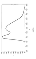
- ein Spektrum einer Versuchslampe gemäß Fig. 1a - 1c
- Fig. 3a
- ein zweites Ausführungsbeispiel einer dielektrischen Barriere-Entladungslampe in Seitenansicht,
- Fig. 3b
- einen Querschnitt der Lampe aus Fig. 3a entlang der Linie AB,
- Fig. 3c
- eine Ausschnittsvergrößerung des Querschnitts aus Fig. 3b.
- Bei der nachfolgenden Erläuterung eines Ausführungsbeispiels der Erfindung wird Bezug auf die Figuren 1a - 1c genommen.
- Die Entladungslampe 1 weist ein rohrförmiges beidseitig verschlossenes Entladungsgefäß 2 mit einem Außendurchmesser von ca. 10 mm auf. Das Entladungsgefäß 2 besteht aus Natronkalkglas und ist mit Xenon mit einem Druck von ca. 15 kPa als Entladungsmedium gefüllt. Auf der Außenseite der Wand des Entladungsgefäßes 2 sind zwei als linienförmige Leiterbahnen ausgebildete metallische Elektroden 3a, 3b diametral zueinander und parallel zur Längsachse des Entladungsgefäßes aufgebracht. Auf der Innenseite der Wand des Entladungsgefäßes 2 (ca. 450 cm2) sind eine "innere" Leuchtstoffschicht 4 und eine "äußere" Leuchtstoffschicht 5 aufgebracht. Die "äußere", bezüglich des Entladungsmediums erste Leuchtstoffschicht 5 besteht aus der Gelb-Leuchtstoffkomponente YAG:Ce. Die "innere", bezüglich des Entladungsmediums zweite Leuchtstoffschicht 4 besteht aus BaMgAl10O16:Eu.
- Von diesem Lampentyp I wurden mehrere Versuchslampen mit unterschiedlichen Schichtgewichten bzw. Verhältnissen der Schichtgewichte der beiden Schichten 4 bzw. 5 gefertigt. Die Koordinaten der damit erzielten Farbörter (nach CIE-Normfarbtafel) sind in der nachfolgende Tabelle aufgeführt.
Lampe-Nr. Schicht 5 (mg/cm2) Schicht 4 (mg/cm2) Verhältnis Schicht 4/5 x y 1 2,69 3,22 1,20 0,420 0,501 2 2,87 3,07 1,07 0,423 0,501 3 3,02 2,84 0,94 0,424 0,500 4 1,78 2,91 1,64 0,415 0,498 5 1,11 3,00 2,70 0,391 0,474 6 1,27 2,82 2,23 0,402 0,490 7 0,62 2,44 3,93 0,336 0,395 8 0,69 2,62 3,81 0,343 0,408 9 0,76 2,73 3,62 0,356 0,425 10 0,49 2,84 5,82 0,309 0,355 11 0,49 2,98 6,09 0,317 0,367 12 0,38 3,07 8,12 0,290 0,328 - Mit der Lampe Nr. 12 wurde gegenüber einer vergleichbaren Standard RGB-Lampe ein korrigierter Helligkeitszuwachs von 13 % erzielt. Das gemessene Spektrum dieser Lampe ist in der Figur 2 dargestellt. Dabei zeigen die Y- und die X-Achse die relative Energie bzw. die Wellenlänge in nm.
- Für die nachfolgenden Erläuterung eines weiteren Ausführungsbeispiels der Erfindung wird Bezug auf die Figuren 3a - 3c genommen.
- Hier sind die beiden Leuchtstoffkomponenten in der umgekehrten Reihenfolge wie im ersten Ausführungsbeispiel aufgebracht, d.h. die "äußere", bezüglich des Entladungsmediums erste Leuchtstoffschicht 7 besteht aus der Blau-Leuchtstoffkomponente BaMgAl10O16:Eu. Die "innere", bezüglich des Entladungsmediums zweite Leuchtstoffschicht 6 besteht aus der Gelb-Leuchtstoffkomponente YAG:Ce. Von diesem Lampentyp 11 wurden mehrere Versuchslampen mit unterschiedlichem Schichtdicken-Verhältnis von Blauund Gelb-Leuchtstoff gefertigt. Die Koordinaten der damit erzielten Farbörter (nach CIE-Normfarbtafel) sind in der nachfolgenden Tabelle aufgeführt. Die Schichtdicken sind dabei wie allgemein üblich durch die entsprechenden Schichtgewichte ausgedrückt.
Lampe-Nr. Schicht 7 (mg/cm2) Schicht 6 (mg/cm2) Verhältnis Schicht 6 / 7 x y 13 3,20 0,36 0,11 0,201 0,182 14 3,36 0,39 0,12 0,209 0,195 15 3,39 0,45 0,13 0,209 0,194 16 3,34 1,00 0,30 0,276 0,300 17 3,39 1,00 0,29 0,287 0,312 18 3,27 0,88 0,27 0,275 0,296 - Ein weiteres Ausführungsbeispiel betrifft eine Variante (nicht dargestellt) der Lampe aus den beiden vorherigen Ausführungsbeispielen, allerdings mit nur einer Leuchtstoffschicht, in der die Blau-Leuchtstoffkomponente BaMg-A|10O16:Eu (BAM) und die Gelb-Leuchtstoffkomponente YAG:Ce (YAG) gemischt sind.
- Von diesem Lampentyp III wurden ebenfalls mehrere Versuchslampen mit unterschiedlichem Verhältnis von Blau- und Gelb-Leuchtstoff gefertigt. Die Koordinaten der damit erzielten Farbörter (nach CIE-Normfarbtafel) sind in der nachfolgenden Tabelle aufgeführt.
Lampe-Nr. Schicht (mg/cm2) Verhältnis BAM/YAG x y 19 3,18 95/5 0,194 0,174 20 3,27 95/5 0,198 0,183 21 3,27 85/15 0,283 0,310 22 3,32 85/15 0,288 0,317 23 3,14 85/15 0,284 0,311 24 3,36 75/25 0,337 0,383 25 3,22 75/25 0,329 0,373 26 3,09 75/25 0,327 0,370 - Die nachfolgende Tabelle zeigt eine Übersicht der Maintenance-Daten der Versuchslampen aus den oben beschriebenen Ausführungsbeispielen nach 100 bzw. 500 Stunden Brenndauer. Wie zu ersehen ist, zeigen alle drei Typen (I, II, III) der Zweibandenlampen gegenüber der verglichenen konventionellen Dreibandenausführung (RGB) eine erhöhte Farbortstabilität, wobei diejenige Ausführung, bei der die Blau-Leuchtstoffschicht der Entladung zugewandt ist (Typ II), zwar den höchsten Lichtstrom-Rückgang, jedoch gleichzeitig die höchste Farbortstabilität aufweist.
Lampentyp 0-100h 0 - 500 h Rel. Lichtstrom (%) Δx Δy Rel. Lichtstrom (%) Δx Δy I -7% 0,003 0,002 -8% 0,003 0,002 II -7% -0,001 0,003 -12% -0,001 0,003 III -4% 0,003 0,002 -8% 0,003 0,003 RGB -5% 0,006 0,005 -7% 0,007 0,009 - Vorstehend wurde die Erfindung zwar am Beispiel einer rohrförmigen Entladungslampe erläutert. Gleichwohl ist die Erfindung nicht auf diesen Lampentyp beschränkt. Vielmehr entfaltet die Erfindung ihre vorteilhafte Wirkung unabhängig von der Form des Entladungsgefäßes. Deshalb sind beispielsweise flächige Lampenformen, wie z.B. in der Schrift US-A 5 994 849 offenbart, genauso geeignet. Außerdem spielt es keine prinzipielle Rolle, ob die Elektroden auf der Außenseite der Entladungsgefäßwand oder alternativ auf der Innenseite angeordnet und mit einer dielektrischen Schicht bedeckt sind. Ebenso können die Elektroden auch völlig unbehindert sein. Ausschlaggebend ist im Zusammenhang mit der eingangs thematisierten Problematik nur, dass das Entladungsmedium im Lampenbetrieb VUV-Strahlung emittiert. Allerdings haben dielektrische Barriere-Entladungslampen diesbezüglich eine gewisse Vorzugsstellung, weil sich damit, wie eingangs bereits erwähnt, in einem speziellen gepulsten Betrieb besonders effizient VUV-Strahlung erzeugen lässt.
Claims (12)
- Entladungslampe (1; 1') mit• einem Entladungsgefäß (2; 2'),• einem Entladungsmedium, das sich im Innern des Entladungsgefäßes (2; 2') befindet und im Betrieb der Lampe elektromagnetische Strahlung im VUV-Bereich emittiert,• einem Leuchtstoff (4 - 7), der auf der Wand des Entladungsgefäßes (2; 2') aufgebracht ist,dadurch gekennzeichnet, dass• der Leuchtstoff (4 - 7) aus einer Gelb- und einer Blau-Leuchtstoffkomponente besteht.
- Entladungslampe nach Anspruch 1, wobei die beiden Leuchtstoffkomponenten in je einer separaten Leuchtstoffschicht, d.h. in einer Gelb- (5; 6) und einer Blau-Leuchtstoffschicht (4; 7) aufgebracht sind.
- Entladungslampe nach Anspruch 2, wobei die Reihenfolge der Leuchtstoffschichten (4; 5) so ist, dass vom Entladungsmedium aus betrachtet zuerst die Gelb-Leuchtstoffschicht (5) und danach die Blau-Leuchtstoffschicht (4) kommt.
- Entladungslampe nach Anspruch 2 oder 3, wobei beide Leuchtstoffschichten (4, 5) auf der Innenseite der Wand des Entladungsgefäßes (2) aufgebracht sind und zwar die Blau-Leuchtstoffschicht (4) unterhalb der Gelb-Leuchtstoffschicht (5).
- Entladungslampe nach Anspruch 2, wobei beide Leuchtstoffschichten (6, 7) auf der Innenseite der Wand des Entladungsgefäßes (2') aufgebracht sind und zwar die Gelb-Leuchtstoffschicht (6) unterhalb der Blau-Leuchtstoffschicht (7) und wobei die Dicke der "äußeren" Blau-Leuchtstoffschicht (7) so gewählt ist, die "innere" Gelb-Leuchtstoffschicht (6) durch die Blau-Leuchtstoffschicht (7) im wesentlichen vollständig von der VUV-Strahlung abgeschirmt ist.
- Entladungslampe nach Anspruch 1, wobei die beiden Leuchtstoffkomponenten in einer gemeinsamen Leuchtstoffschicht gemischt sind.
- Entladungslampe nach einem der Ansprüche 1 bis 6, mit der Gelb-Leuchtstoffkomponente
(Y, Gd, Tb)AG:Ce. - Entladungslampe nach einem der Ansprüche 1 bis 7, mit der Blau-Leuchtstoffkomponente
BaMgAl10O17:Eu. - Entladungslampe nach einem der Ansprüche 1 bis 7, mit der Blau-Leuchtstoffkomponente
SrMgAl10O17:Eu. - Entladungslampe nach einem der Ansprüche 1 bis 7, mit der Blau-Leuchtstoffkomponente
(Ba, Sr)MgAl10O17:Eu. - Entladungslampe nach einem der vorstehenden Ansprüche, wobei das Entladungsmedium das Edelgas Xenon umfasst.
- Entladungslampe nach einem der vorstehenden Ansprüche, die als dielektrische Barrieren-Entladungslampe ausgelegt ist.
Applications Claiming Priority (2)
| Application Number | Priority Date | Filing Date | Title |
|---|---|---|---|
| DE10326755 | 2003-06-13 | ||
| DE10326755A DE10326755A1 (de) | 2003-06-13 | 2003-06-13 | Entladungslampe mit Zweibanden-Leuchtstoff |
Publications (3)
| Publication Number | Publication Date |
|---|---|
| EP1491611A2 true EP1491611A2 (de) | 2004-12-29 |
| EP1491611A3 EP1491611A3 (de) | 2005-04-06 |
| EP1491611B1 EP1491611B1 (de) | 2007-07-04 |
Family
ID=33394825
Family Applications (1)
| Application Number | Title | Priority Date | Filing Date |
|---|---|---|---|
| EP04009453A Expired - Lifetime EP1491611B1 (de) | 2003-06-13 | 2004-04-21 | Entladungslampe mit Zweibanden-Leuchtstoff |
Country Status (8)
| Country | Link |
|---|---|
| US (1) | US7199513B2 (de) |
| EP (1) | EP1491611B1 (de) |
| JP (1) | JP4732713B2 (de) |
| KR (1) | KR101078174B1 (de) |
| CN (1) | CN100431091C (de) |
| CA (1) | CA2470301C (de) |
| DE (2) | DE10326755A1 (de) |
| TW (1) | TWI288944B (de) |
Cited By (1)
| Publication number | Priority date | Publication date | Assignee | Title |
|---|---|---|---|---|
| WO2007125471A3 (en) * | 2006-05-01 | 2009-02-05 | Koninkl Philips Electronics Nv | Low-pressure discharge lamp |
Families Citing this family (288)
| Publication number | Priority date | Publication date | Assignee | Title |
|---|---|---|---|---|
| DE10236420A1 (de) * | 2002-08-08 | 2004-02-19 | Patent-Treuhand-Gesellschaft für elektrische Glühlampen mbH | Dielektrische Barriere-Entladungslampe mit verbesserter Farbwiedergabe |
| DE10324832A1 (de) * | 2003-06-02 | 2004-12-23 | Patent-Treuhand-Gesellschaft für elektrische Glühlampen mbH | Entladungslampe mit Leuchtstoff |
| JP5274947B2 (ja) * | 2008-09-17 | 2013-08-28 | 三菱電機照明株式会社 | 蛍光ランプ |
| US20130023129A1 (en) | 2011-07-20 | 2013-01-24 | Asm America, Inc. | Pressure transmitter for a semiconductor processing environment |
| US20140099798A1 (en) * | 2012-10-05 | 2014-04-10 | Asm Ip Holding B.V. | UV-Curing Apparatus Provided With Wavelength-Tuned Excimer Lamp and Method of Processing Semiconductor Substrate Using Same |
| US10714315B2 (en) | 2012-10-12 | 2020-07-14 | Asm Ip Holdings B.V. | Semiconductor reaction chamber showerhead |
| US20160376700A1 (en) | 2013-02-01 | 2016-12-29 | Asm Ip Holding B.V. | System for treatment of deposition reactor |
| US11015245B2 (en) | 2014-03-19 | 2021-05-25 | Asm Ip Holding B.V. | Gas-phase reactor and system having exhaust plenum and components thereof |
| US10858737B2 (en) | 2014-07-28 | 2020-12-08 | Asm Ip Holding B.V. | Showerhead assembly and components thereof |
| US10941490B2 (en) | 2014-10-07 | 2021-03-09 | Asm Ip Holding B.V. | Multiple temperature range susceptor, assembly, reactor and system including the susceptor, and methods of using the same |
| US10276355B2 (en) | 2015-03-12 | 2019-04-30 | Asm Ip Holding B.V. | Multi-zone reactor, system including the reactor, and method of using the same |
| US10458018B2 (en) | 2015-06-26 | 2019-10-29 | Asm Ip Holding B.V. | Structures including metal carbide material, devices including the structures, and methods of forming same |
| US10211308B2 (en) | 2015-10-21 | 2019-02-19 | Asm Ip Holding B.V. | NbMC layers |
| US11139308B2 (en) | 2015-12-29 | 2021-10-05 | Asm Ip Holding B.V. | Atomic layer deposition of III-V compounds to form V-NAND devices |
| US10529554B2 (en) | 2016-02-19 | 2020-01-07 | Asm Ip Holding B.V. | Method for forming silicon nitride film selectively on sidewalls or flat surfaces of trenches |
| US10343920B2 (en) | 2016-03-18 | 2019-07-09 | Asm Ip Holding B.V. | Aligned carbon nanotubes |
| US10367080B2 (en) | 2016-05-02 | 2019-07-30 | Asm Ip Holding B.V. | Method of forming a germanium oxynitride film |
| US11453943B2 (en) | 2016-05-25 | 2022-09-27 | Asm Ip Holding B.V. | Method for forming carbon-containing silicon/metal oxide or nitride film by ALD using silicon precursor and hydrocarbon precursor |
| US10612137B2 (en) | 2016-07-08 | 2020-04-07 | Asm Ip Holdings B.V. | Organic reactants for atomic layer deposition |
| US9859151B1 (en) | 2016-07-08 | 2018-01-02 | Asm Ip Holding B.V. | Selective film deposition method to form air gaps |
| KR102532607B1 (ko) | 2016-07-28 | 2023-05-15 | 에이에스엠 아이피 홀딩 비.브이. | 기판 가공 장치 및 그 동작 방법 |
| US9812320B1 (en) | 2016-07-28 | 2017-11-07 | Asm Ip Holding B.V. | Method and apparatus for filling a gap |
| US9887082B1 (en) | 2016-07-28 | 2018-02-06 | Asm Ip Holding B.V. | Method and apparatus for filling a gap |
| US11532757B2 (en) | 2016-10-27 | 2022-12-20 | Asm Ip Holding B.V. | Deposition of charge trapping layers |
| US10714350B2 (en) | 2016-11-01 | 2020-07-14 | ASM IP Holdings, B.V. | Methods for forming a transition metal niobium nitride film on a substrate by atomic layer deposition and related semiconductor device structures |
| KR102546317B1 (ko) | 2016-11-15 | 2023-06-21 | 에이에스엠 아이피 홀딩 비.브이. | 기체 공급 유닛 및 이를 포함하는 기판 처리 장치 |
| KR102762543B1 (ko) | 2016-12-14 | 2025-02-05 | 에이에스엠 아이피 홀딩 비.브이. | 기판 처리 장치 |
| US11581186B2 (en) | 2016-12-15 | 2023-02-14 | Asm Ip Holding B.V. | Sequential infiltration synthesis apparatus |
| US11447861B2 (en) | 2016-12-15 | 2022-09-20 | Asm Ip Holding B.V. | Sequential infiltration synthesis apparatus and a method of forming a patterned structure |
| KR102700194B1 (ko) | 2016-12-19 | 2024-08-28 | 에이에스엠 아이피 홀딩 비.브이. | 기판 처리 장치 |
| US10269558B2 (en) | 2016-12-22 | 2019-04-23 | Asm Ip Holding B.V. | Method of forming a structure on a substrate |
| US11390950B2 (en) | 2017-01-10 | 2022-07-19 | Asm Ip Holding B.V. | Reactor system and method to reduce residue buildup during a film deposition process |
| US10468261B2 (en) | 2017-02-15 | 2019-11-05 | Asm Ip Holding B.V. | Methods for forming a metallic film on a substrate by cyclical deposition and related semiconductor device structures |
| US10529563B2 (en) | 2017-03-29 | 2020-01-07 | Asm Ip Holdings B.V. | Method for forming doped metal oxide films on a substrate by cyclical deposition and related semiconductor device structures |
| US10770286B2 (en) | 2017-05-08 | 2020-09-08 | Asm Ip Holdings B.V. | Methods for selectively forming a silicon nitride film on a substrate and related semiconductor device structures |
| US12040200B2 (en) | 2017-06-20 | 2024-07-16 | Asm Ip Holding B.V. | Semiconductor processing apparatus and methods for calibrating a semiconductor processing apparatus |
| US11306395B2 (en) | 2017-06-28 | 2022-04-19 | Asm Ip Holding B.V. | Methods for depositing a transition metal nitride film on a substrate by atomic layer deposition and related deposition apparatus |
| TWI794238B (zh) | 2017-07-13 | 2023-03-01 | 荷蘭商Asm智慧財產控股公司 | 於單一加工腔室中自半導體膜移除氧化物及碳之裝置及方法 |
| KR20190009245A (ko) | 2017-07-18 | 2019-01-28 | 에이에스엠 아이피 홀딩 비.브이. | 반도체 소자 구조물 형성 방법 및 관련된 반도체 소자 구조물 |
| US11374112B2 (en) | 2017-07-19 | 2022-06-28 | Asm Ip Holding B.V. | Method for depositing a group IV semiconductor and related semiconductor device structures |
| US11018002B2 (en) | 2017-07-19 | 2021-05-25 | Asm Ip Holding B.V. | Method for selectively depositing a Group IV semiconductor and related semiconductor device structures |
| US10541333B2 (en) | 2017-07-19 | 2020-01-21 | Asm Ip Holding B.V. | Method for depositing a group IV semiconductor and related semiconductor device structures |
| US10590535B2 (en) | 2017-07-26 | 2020-03-17 | Asm Ip Holdings B.V. | Chemical treatment, deposition and/or infiltration apparatus and method for using the same |
| TWI815813B (zh) | 2017-08-04 | 2023-09-21 | 荷蘭商Asm智慧財產控股公司 | 用於分配反應腔內氣體的噴頭總成 |
| US10770336B2 (en) | 2017-08-08 | 2020-09-08 | Asm Ip Holding B.V. | Substrate lift mechanism and reactor including same |
| US10692741B2 (en) | 2017-08-08 | 2020-06-23 | Asm Ip Holdings B.V. | Radiation shield |
| US11769682B2 (en) | 2017-08-09 | 2023-09-26 | Asm Ip Holding B.V. | Storage apparatus for storing cassettes for substrates and processing apparatus equipped therewith |
| US11139191B2 (en) | 2017-08-09 | 2021-10-05 | Asm Ip Holding B.V. | Storage apparatus for storing cassettes for substrates and processing apparatus equipped therewith |
| US11830730B2 (en) | 2017-08-29 | 2023-11-28 | Asm Ip Holding B.V. | Layer forming method and apparatus |
| US11056344B2 (en) | 2017-08-30 | 2021-07-06 | Asm Ip Holding B.V. | Layer forming method |
| KR102491945B1 (ko) | 2017-08-30 | 2023-01-26 | 에이에스엠 아이피 홀딩 비.브이. | 기판 처리 장치 |
| US11295980B2 (en) | 2017-08-30 | 2022-04-05 | Asm Ip Holding B.V. | Methods for depositing a molybdenum metal film over a dielectric surface of a substrate by a cyclical deposition process and related semiconductor device structures |
| US10658205B2 (en) | 2017-09-28 | 2020-05-19 | Asm Ip Holdings B.V. | Chemical dispensing apparatus and methods for dispensing a chemical to a reaction chamber |
| US10403504B2 (en) | 2017-10-05 | 2019-09-03 | Asm Ip Holding B.V. | Method for selectively depositing a metallic film on a substrate |
| US10923344B2 (en) | 2017-10-30 | 2021-02-16 | Asm Ip Holding B.V. | Methods for forming a semiconductor structure and related semiconductor structures |
| US11022879B2 (en) | 2017-11-24 | 2021-06-01 | Asm Ip Holding B.V. | Method of forming an enhanced unexposed photoresist layer |
| TWI791689B (zh) | 2017-11-27 | 2023-02-11 | 荷蘭商Asm智慧財產控股私人有限公司 | 包括潔淨迷你環境之裝置 |
| WO2019103613A1 (en) | 2017-11-27 | 2019-05-31 | Asm Ip Holding B.V. | A storage device for storing wafer cassettes for use with a batch furnace |
| US10872771B2 (en) | 2018-01-16 | 2020-12-22 | Asm Ip Holding B. V. | Method for depositing a material film on a substrate within a reaction chamber by a cyclical deposition process and related device structures |
| TWI799494B (zh) | 2018-01-19 | 2023-04-21 | 荷蘭商Asm 智慧財產控股公司 | 沈積方法 |
| US11482412B2 (en) | 2018-01-19 | 2022-10-25 | Asm Ip Holding B.V. | Method for depositing a gap-fill layer by plasma-assisted deposition |
| US11081345B2 (en) | 2018-02-06 | 2021-08-03 | Asm Ip Holding B.V. | Method of post-deposition treatment for silicon oxide film |
| US10896820B2 (en) | 2018-02-14 | 2021-01-19 | Asm Ip Holding B.V. | Method for depositing a ruthenium-containing film on a substrate by a cyclical deposition process |
| WO2019158960A1 (en) | 2018-02-14 | 2019-08-22 | Asm Ip Holding B.V. | A method for depositing a ruthenium-containing film on a substrate by a cyclical deposition process |
| US10731249B2 (en) | 2018-02-15 | 2020-08-04 | Asm Ip Holding B.V. | Method of forming a transition metal containing film on a substrate by a cyclical deposition process, a method for supplying a transition metal halide compound to a reaction chamber, and related vapor deposition apparatus |
| KR102636427B1 (ko) | 2018-02-20 | 2024-02-13 | 에이에스엠 아이피 홀딩 비.브이. | 기판 처리 방법 및 장치 |
| US10975470B2 (en) | 2018-02-23 | 2021-04-13 | Asm Ip Holding B.V. | Apparatus for detecting or monitoring for a chemical precursor in a high temperature environment |
| US11473195B2 (en) | 2018-03-01 | 2022-10-18 | Asm Ip Holding B.V. | Semiconductor processing apparatus and a method for processing a substrate |
| US11629406B2 (en) | 2018-03-09 | 2023-04-18 | Asm Ip Holding B.V. | Semiconductor processing apparatus comprising one or more pyrometers for measuring a temperature of a substrate during transfer of the substrate |
| US11114283B2 (en) | 2018-03-16 | 2021-09-07 | Asm Ip Holding B.V. | Reactor, system including the reactor, and methods of manufacturing and using same |
| KR102646467B1 (ko) | 2018-03-27 | 2024-03-11 | 에이에스엠 아이피 홀딩 비.브이. | 기판 상에 전극을 형성하는 방법 및 전극을 포함하는 반도체 소자 구조 |
| US11088002B2 (en) | 2018-03-29 | 2021-08-10 | Asm Ip Holding B.V. | Substrate rack and a substrate processing system and method |
| US11230766B2 (en) | 2018-03-29 | 2022-01-25 | Asm Ip Holding B.V. | Substrate processing apparatus and method |
| KR102600229B1 (ko) | 2018-04-09 | 2023-11-10 | 에이에스엠 아이피 홀딩 비.브이. | 기판 지지 장치, 이를 포함하는 기판 처리 장치 및 기판 처리 방법 |
| TWI843623B (zh) | 2018-05-08 | 2024-05-21 | 荷蘭商Asm Ip私人控股有限公司 | 藉由循環沉積製程於基板上沉積氧化物膜之方法及相關裝置結構 |
| US12025484B2 (en) | 2018-05-08 | 2024-07-02 | Asm Ip Holding B.V. | Thin film forming method |
| US12272527B2 (en) | 2018-05-09 | 2025-04-08 | Asm Ip Holding B.V. | Apparatus for use with hydrogen radicals and method of using same |
| KR102596988B1 (ko) | 2018-05-28 | 2023-10-31 | 에이에스엠 아이피 홀딩 비.브이. | 기판 처리 방법 및 그에 의해 제조된 장치 |
| TWI840362B (zh) | 2018-06-04 | 2024-05-01 | 荷蘭商Asm Ip私人控股有限公司 | 水氣降低的晶圓處置腔室 |
| US11718913B2 (en) | 2018-06-04 | 2023-08-08 | Asm Ip Holding B.V. | Gas distribution system and reactor system including same |
| US11286562B2 (en) | 2018-06-08 | 2022-03-29 | Asm Ip Holding B.V. | Gas-phase chemical reactor and method of using same |
| US10797133B2 (en) | 2018-06-21 | 2020-10-06 | Asm Ip Holding B.V. | Method for depositing a phosphorus doped silicon arsenide film and related semiconductor device structures |
| KR102568797B1 (ko) | 2018-06-21 | 2023-08-21 | 에이에스엠 아이피 홀딩 비.브이. | 기판 처리 시스템 |
| WO2020003000A1 (en) | 2018-06-27 | 2020-01-02 | Asm Ip Holding B.V. | Cyclic deposition methods for forming metal-containing material and films and structures including the metal-containing material |
| KR20250134000A (ko) | 2018-06-27 | 2025-09-09 | 에이에스엠 아이피 홀딩 비.브이. | 금속 함유 재료를 형성하기 위한 주기적 증착 방법 및 금속 함유 재료를 포함하는 필름 및 구조체 |
| US10612136B2 (en) | 2018-06-29 | 2020-04-07 | ASM IP Holding, B.V. | Temperature-controlled flange and reactor system including same |
| US10388513B1 (en) | 2018-07-03 | 2019-08-20 | Asm Ip Holding B.V. | Method for depositing silicon-free carbon-containing film as gap-fill layer by pulse plasma-assisted deposition |
| US10755922B2 (en) | 2018-07-03 | 2020-08-25 | Asm Ip Holding B.V. | Method for depositing silicon-free carbon-containing film as gap-fill layer by pulse plasma-assisted deposition |
| US11053591B2 (en) | 2018-08-06 | 2021-07-06 | Asm Ip Holding B.V. | Multi-port gas injection system and reactor system including same |
| US11430674B2 (en) | 2018-08-22 | 2022-08-30 | Asm Ip Holding B.V. | Sensor array, apparatus for dispensing a vapor phase reactant to a reaction chamber and related methods |
| KR102707956B1 (ko) | 2018-09-11 | 2024-09-19 | 에이에스엠 아이피 홀딩 비.브이. | 박막 증착 방법 |
| US11024523B2 (en) | 2018-09-11 | 2021-06-01 | Asm Ip Holding B.V. | Substrate processing apparatus and method |
| US11049751B2 (en) | 2018-09-14 | 2021-06-29 | Asm Ip Holding B.V. | Cassette supply system to store and handle cassettes and processing apparatus equipped therewith |
| CN110970344B (zh) | 2018-10-01 | 2024-10-25 | Asmip控股有限公司 | 衬底保持设备、包含所述设备的系统及其使用方法 |
| US11232963B2 (en) | 2018-10-03 | 2022-01-25 | Asm Ip Holding B.V. | Substrate processing apparatus and method |
| KR102592699B1 (ko) | 2018-10-08 | 2023-10-23 | 에이에스엠 아이피 홀딩 비.브이. | 기판 지지 유닛 및 이를 포함하는 박막 증착 장치와 기판 처리 장치 |
| KR102605121B1 (ko) | 2018-10-19 | 2023-11-23 | 에이에스엠 아이피 홀딩 비.브이. | 기판 처리 장치 및 기판 처리 방법 |
| KR102546322B1 (ko) | 2018-10-19 | 2023-06-21 | 에이에스엠 아이피 홀딩 비.브이. | 기판 처리 장치 및 기판 처리 방법 |
| USD948463S1 (en) | 2018-10-24 | 2022-04-12 | Asm Ip Holding B.V. | Susceptor for semiconductor substrate supporting apparatus |
| US12378665B2 (en) | 2018-10-26 | 2025-08-05 | Asm Ip Holding B.V. | High temperature coatings for a preclean and etch apparatus and related methods |
| US11087997B2 (en) | 2018-10-31 | 2021-08-10 | Asm Ip Holding B.V. | Substrate processing apparatus for processing substrates |
| KR102748291B1 (ko) | 2018-11-02 | 2024-12-31 | 에이에스엠 아이피 홀딩 비.브이. | 기판 지지 유닛 및 이를 포함하는 기판 처리 장치 |
| US11572620B2 (en) | 2018-11-06 | 2023-02-07 | Asm Ip Holding B.V. | Methods for selectively depositing an amorphous silicon film on a substrate |
| US11031242B2 (en) | 2018-11-07 | 2021-06-08 | Asm Ip Holding B.V. | Methods for depositing a boron doped silicon germanium film |
| US10847366B2 (en) | 2018-11-16 | 2020-11-24 | Asm Ip Holding B.V. | Methods for depositing a transition metal chalcogenide film on a substrate by a cyclical deposition process |
| US10818758B2 (en) | 2018-11-16 | 2020-10-27 | Asm Ip Holding B.V. | Methods for forming a metal silicate film on a substrate in a reaction chamber and related semiconductor device structures |
| US12040199B2 (en) | 2018-11-28 | 2024-07-16 | Asm Ip Holding B.V. | Substrate processing apparatus for processing substrates |
| US11217444B2 (en) | 2018-11-30 | 2022-01-04 | Asm Ip Holding B.V. | Method for forming an ultraviolet radiation responsive metal oxide-containing film |
| KR102636428B1 (ko) | 2018-12-04 | 2024-02-13 | 에이에스엠 아이피 홀딩 비.브이. | 기판 처리 장치를 세정하는 방법 |
| US11158513B2 (en) | 2018-12-13 | 2021-10-26 | Asm Ip Holding B.V. | Methods for forming a rhenium-containing film on a substrate by a cyclical deposition process and related semiconductor device structures |
| JP7504584B2 (ja) | 2018-12-14 | 2024-06-24 | エーエスエム・アイピー・ホールディング・ベー・フェー | 窒化ガリウムの選択的堆積を用いてデバイス構造体を形成する方法及びそのためのシステム |
| TWI866480B (zh) | 2019-01-17 | 2024-12-11 | 荷蘭商Asm Ip 私人控股有限公司 | 藉由循環沈積製程於基板上形成含過渡金屬膜之方法 |
| KR102727227B1 (ko) | 2019-01-22 | 2024-11-07 | 에이에스엠 아이피 홀딩 비.브이. | 기판 처리 장치 |
| CN111524788B (zh) | 2019-02-01 | 2023-11-24 | Asm Ip私人控股有限公司 | 氧化硅的拓扑选择性膜形成的方法 |
| KR102638425B1 (ko) | 2019-02-20 | 2024-02-21 | 에이에스엠 아이피 홀딩 비.브이. | 기판 표면 내에 형성된 오목부를 충진하기 위한 방법 및 장치 |
| KR102626263B1 (ko) | 2019-02-20 | 2024-01-16 | 에이에스엠 아이피 홀딩 비.브이. | 처리 단계를 포함하는 주기적 증착 방법 및 이를 위한 장치 |
| TWI838458B (zh) | 2019-02-20 | 2024-04-11 | 荷蘭商Asm Ip私人控股有限公司 | 用於3d nand應用中之插塞填充沉積之設備及方法 |
| TWI845607B (zh) | 2019-02-20 | 2024-06-21 | 荷蘭商Asm Ip私人控股有限公司 | 用來填充形成於基材表面內之凹部的循環沉積方法及設備 |
| TWI842826B (zh) | 2019-02-22 | 2024-05-21 | 荷蘭商Asm Ip私人控股有限公司 | 基材處理設備及處理基材之方法 |
| KR102782593B1 (ko) | 2019-03-08 | 2025-03-14 | 에이에스엠 아이피 홀딩 비.브이. | SiOC 층을 포함한 구조체 및 이의 형성 방법 |
| US11742198B2 (en) | 2019-03-08 | 2023-08-29 | Asm Ip Holding B.V. | Structure including SiOCN layer and method of forming same |
| KR102858005B1 (ko) | 2019-03-08 | 2025-09-09 | 에이에스엠 아이피 홀딩 비.브이. | 실리콘 질화물 층을 선택적으로 증착하는 방법, 및 선택적으로 증착된 실리콘 질화물 층을 포함하는 구조체 |
| JP2020167398A (ja) | 2019-03-28 | 2020-10-08 | エーエスエム・アイピー・ホールディング・ベー・フェー | ドアオープナーおよびドアオープナーが提供される基材処理装置 |
| KR102809999B1 (ko) | 2019-04-01 | 2025-05-19 | 에이에스엠 아이피 홀딩 비.브이. | 반도체 소자를 제조하는 방법 |
| KR102897355B1 (ko) | 2019-04-19 | 2025-12-08 | 에이에스엠 아이피 홀딩 비.브이. | 층 형성 방법 및 장치 |
| KR20200125453A (ko) | 2019-04-24 | 2020-11-04 | 에이에스엠 아이피 홀딩 비.브이. | 기상 반응기 시스템 및 이를 사용하는 방법 |
| KR102869364B1 (ko) | 2019-05-07 | 2025-10-10 | 에이에스엠 아이피 홀딩 비.브이. | 비정질 탄소 중합체 막을 개질하는 방법 |
| KR102929471B1 (ko) | 2019-05-07 | 2026-02-20 | 에이에스엠 아이피 홀딩 비.브이. | 딥 튜브가 있는 화학물질 공급원 용기 |
| KR102929472B1 (ko) | 2019-05-10 | 2026-02-20 | 에이에스엠 아이피 홀딩 비.브이. | 표면 상에 재료를 증착하는 방법 및 본 방법에 따라 형성된 구조 |
| JP7598201B2 (ja) | 2019-05-16 | 2024-12-11 | エーエスエム・アイピー・ホールディング・ベー・フェー | ウェハボートハンドリング装置、縦型バッチ炉および方法 |
| JP7612342B2 (ja) | 2019-05-16 | 2025-01-14 | エーエスエム・アイピー・ホールディング・ベー・フェー | ウェハボートハンドリング装置、縦型バッチ炉および方法 |
| USD975665S1 (en) | 2019-05-17 | 2023-01-17 | Asm Ip Holding B.V. | Susceptor shaft |
| USD947913S1 (en) | 2019-05-17 | 2022-04-05 | Asm Ip Holding B.V. | Susceptor shaft |
| USD935572S1 (en) | 2019-05-24 | 2021-11-09 | Asm Ip Holding B.V. | Gas channel plate |
| USD922229S1 (en) | 2019-06-05 | 2021-06-15 | Asm Ip Holding B.V. | Device for controlling a temperature of a gas supply unit |
| KR20200141003A (ko) | 2019-06-06 | 2020-12-17 | 에이에스엠 아이피 홀딩 비.브이. | 가스 감지기를 포함하는 기상 반응기 시스템 |
| KR102918757B1 (ko) | 2019-06-10 | 2026-01-28 | 에이에스엠 아이피 홀딩 비.브이. | 석영 에피택셜 챔버를 세정하는 방법 |
| KR20200143254A (ko) | 2019-06-11 | 2020-12-23 | 에이에스엠 아이피 홀딩 비.브이. | 개질 가스를 사용하여 전자 구조를 형성하는 방법, 상기 방법을 수행하기 위한 시스템, 및 상기 방법을 사용하여 형성되는 구조 |
| USD944946S1 (en) | 2019-06-14 | 2022-03-01 | Asm Ip Holding B.V. | Shower plate |
| USD931978S1 (en) | 2019-06-27 | 2021-09-28 | Asm Ip Holding B.V. | Showerhead vacuum transport |
| KR102911421B1 (ko) | 2019-07-03 | 2026-01-12 | 에이에스엠 아이피 홀딩 비.브이. | 기판 처리 장치용 온도 제어 조립체 및 이를 사용하는 방법 |
| JP7499079B2 (ja) | 2019-07-09 | 2024-06-13 | エーエスエム・アイピー・ホールディング・ベー・フェー | 同軸導波管を用いたプラズマ装置、基板処理方法 |
| CN112216646B (zh) | 2019-07-10 | 2026-02-10 | Asmip私人控股有限公司 | 基板支撑组件及包括其的基板处理装置 |
| KR102895115B1 (ko) | 2019-07-16 | 2025-12-03 | 에이에스엠 아이피 홀딩 비.브이. | 기판 처리 장치 |
| KR102955799B1 (ko) | 2019-07-17 | 2026-04-21 | 에이에스엠 아이피 홀딩 비.브이. | 라디칼 보조 점화 플라즈마 시스템 및 방법 |
| KR102860110B1 (ko) | 2019-07-17 | 2025-09-16 | 에이에스엠 아이피 홀딩 비.브이. | 실리콘 게르마늄 구조를 형성하는 방법 |
| US11643724B2 (en) | 2019-07-18 | 2023-05-09 | Asm Ip Holding B.V. | Method of forming structures using a neutral beam |
| TWI839544B (zh) | 2019-07-19 | 2024-04-21 | 荷蘭商Asm Ip私人控股有限公司 | 形成形貌受控的非晶碳聚合物膜之方法 |
| KR102903090B1 (ko) | 2019-07-19 | 2025-12-19 | 에이에스엠 아이피 홀딩 비.브이. | 토폴로지-제어된 비정질 탄소 중합체 막을 형성하는 방법 |
| TWI851767B (zh) | 2019-07-29 | 2024-08-11 | 荷蘭商Asm Ip私人控股有限公司 | 用於利用n型摻雜物及/或替代摻雜物選擇性沉積以達成高摻雜物併入之方法 |
| CN112309900B (zh) | 2019-07-30 | 2025-11-04 | Asmip私人控股有限公司 | 基板处理设备 |
| KR102971074B1 (ko) | 2019-07-30 | 2026-05-29 | 에이에스엠 아이피 홀딩 비.브이. | 기판 처리 장치 및 방법 |
| CN112309899B (zh) | 2019-07-30 | 2025-11-14 | Asmip私人控股有限公司 | 基板处理设备 |
| US11227782B2 (en) | 2019-07-31 | 2022-01-18 | Asm Ip Holding B.V. | Vertical batch furnace assembly |
| US12622218B2 (en) | 2019-07-31 | 2026-05-05 | Asm Ip Holding B.V. | Cassette lid opening device |
| US11587814B2 (en) | 2019-07-31 | 2023-02-21 | Asm Ip Holding B.V. | Vertical batch furnace assembly |
| US11587815B2 (en) | 2019-07-31 | 2023-02-21 | Asm Ip Holding B.V. | Vertical batch furnace assembly |
| CN112323048B (zh) | 2019-08-05 | 2024-02-09 | Asm Ip私人控股有限公司 | 用于化学源容器的液位传感器 |
| CN112342526A (zh) | 2019-08-09 | 2021-02-09 | Asm Ip私人控股有限公司 | 包括冷却装置的加热器组件及其使用方法 |
| USD965524S1 (en) | 2019-08-19 | 2022-10-04 | Asm Ip Holding B.V. | Susceptor support |
| USD965044S1 (en) | 2019-08-19 | 2022-09-27 | Asm Ip Holding B.V. | Susceptor shaft |
| JP7810514B2 (ja) | 2019-08-21 | 2026-02-03 | エーエスエム・アイピー・ホールディング・ベー・フェー | 成膜原料混合ガス生成装置及び成膜装置 |
| KR102983146B1 (ko) | 2019-08-22 | 2026-06-26 | 에이에스엠 아이피 홀딩 비.브이. | 홀을 구비한 구조체를 형성하기 위한 방법 |
| USD979506S1 (en) | 2019-08-22 | 2023-02-28 | Asm Ip Holding B.V. | Insulator |
| USD940837S1 (en) | 2019-08-22 | 2022-01-11 | Asm Ip Holding B.V. | Electrode |
| USD930782S1 (en) | 2019-08-22 | 2021-09-14 | Asm Ip Holding B.V. | Gas distributor |
| USD949319S1 (en) | 2019-08-22 | 2022-04-19 | Asm Ip Holding B.V. | Exhaust duct |
| US11286558B2 (en) | 2019-08-23 | 2022-03-29 | Asm Ip Holding B.V. | Methods for depositing a molybdenum nitride film on a surface of a substrate by a cyclical deposition process and related semiconductor device structures including a molybdenum nitride film |
| KR102928101B1 (ko) | 2019-08-23 | 2026-02-13 | 에이에스엠 아이피 홀딩 비.브이. | 비스(디에틸아미노)실란을 사용하여 peald에 의해 개선된 품질을 갖는 실리콘 산화물 막을 증착하기 위한 방법 |
| CN112442674A (zh) | 2019-09-03 | 2021-03-05 | Asm Ip私人控股有限公司 | 用于沉积硫族化物膜的方法和设备以及包括膜的结构 |
| KR102806450B1 (ko) | 2019-09-04 | 2025-05-12 | 에이에스엠 아이피 홀딩 비.브이. | 희생 캡핑 층을 이용한 선택적 증착 방법 |
| KR102733104B1 (ko) | 2019-09-05 | 2024-11-22 | 에이에스엠 아이피 홀딩 비.브이. | 기판 처리 장치 |
| US12469693B2 (en) | 2019-09-17 | 2025-11-11 | Asm Ip Holding B.V. | Method of forming a carbon-containing layer and structure including the layer |
| US11562901B2 (en) | 2019-09-25 | 2023-01-24 | Asm Ip Holding B.V. | Substrate processing method |
| CN112593212B (zh) | 2019-10-02 | 2023-12-22 | Asm Ip私人控股有限公司 | 通过循环等离子体增强沉积工艺形成拓扑选择性氧化硅膜的方法 |
| KR102948143B1 (ko) | 2019-10-08 | 2026-04-07 | 에이에스엠 아이피 홀딩 비.브이. | 활성 종을 이용하기 위한 가스 분배 어셈블리를 포함한 반응기 시스템 및 이를 사용하는 방법 |
| TWI925822B (zh) | 2019-10-08 | 2026-05-21 | 荷蘭商Asm Ip私人控股有限公司 | 氣體注入系統、及將材料沉積於反應室內之基板表面上的方法 |
| TWI846953B (zh) | 2019-10-08 | 2024-07-01 | 荷蘭商Asm Ip私人控股有限公司 | 基板處理裝置 |
| KR102879443B1 (ko) | 2019-10-10 | 2025-11-03 | 에이에스엠 아이피 홀딩 비.브이. | 포토레지스트 하부층을 형성하기 위한 방법 및 이를 포함한 구조체 |
| US12009241B2 (en) | 2019-10-14 | 2024-06-11 | Asm Ip Holding B.V. | Vertical batch furnace assembly with detector to detect cassette |
| TWI834919B (zh) | 2019-10-16 | 2024-03-11 | 荷蘭商Asm Ip私人控股有限公司 | 氧化矽之拓撲選擇性膜形成之方法 |
| US11637014B2 (en) | 2019-10-17 | 2023-04-25 | Asm Ip Holding B.V. | Methods for selective deposition of doped semiconductor material |
| KR102845724B1 (ko) | 2019-10-21 | 2025-08-13 | 에이에스엠 아이피 홀딩 비.브이. | 막을 선택적으로 에칭하기 위한 장치 및 방법 |
| KR102960940B1 (ko) | 2019-10-25 | 2026-05-04 | 에이에스엠 아이피 홀딩 비.브이. | 기판 표면 상의 갭 피처를 충진하는 방법 및 이와 관련된 반도체 소자 구조 |
| US11646205B2 (en) | 2019-10-29 | 2023-05-09 | Asm Ip Holding B.V. | Methods of selectively forming n-type doped material on a surface, systems for selectively forming n-type doped material, and structures formed using same |
| KR102890638B1 (ko) | 2019-11-05 | 2025-11-25 | 에이에스엠 아이피 홀딩 비.브이. | 도핑된 반도체 층을 갖는 구조체 및 이를 형성하기 위한 방법 및 시스템 |
| US11501968B2 (en) | 2019-11-15 | 2022-11-15 | Asm Ip Holding B.V. | Method for providing a semiconductor device with silicon filled gaps |
| KR102861314B1 (ko) | 2019-11-20 | 2025-09-17 | 에이에스엠 아이피 홀딩 비.브이. | 기판의 표면 상에 탄소 함유 물질을 증착하는 방법, 상기 방법을 사용하여 형성된 구조물, 및 상기 구조물을 형성하기 위한 시스템 |
| CN112951697B (zh) | 2019-11-26 | 2025-07-29 | Asmip私人控股有限公司 | 基板处理设备 |
| KR20210065848A (ko) | 2019-11-26 | 2021-06-04 | 에이에스엠 아이피 홀딩 비.브이. | 제1 유전체 표면과 제2 금속성 표면을 포함한 기판 상에 타겟 막을 선택적으로 형성하기 위한 방법 |
| CN120998766A (zh) | 2019-11-29 | 2025-11-21 | Asm Ip私人控股有限公司 | 基板处理设备 |
| CN120432376A (zh) | 2019-11-29 | 2025-08-05 | Asm Ip私人控股有限公司 | 基板处理设备 |
| JP7527928B2 (ja) | 2019-12-02 | 2024-08-05 | エーエスエム・アイピー・ホールディング・ベー・フェー | 基板処理装置、基板処理方法 |
| KR20210070898A (ko) | 2019-12-04 | 2021-06-15 | 에이에스엠 아이피 홀딩 비.브이. | 기판 처리 장치 |
| CN112992667A (zh) | 2019-12-17 | 2021-06-18 | Asm Ip私人控股有限公司 | 形成氮化钒层的方法和包括氮化钒层的结构 |
| KR102943768B1 (ko) | 2019-12-19 | 2026-03-26 | 에이에스엠 아이피 홀딩 비.브이. | 기판 상의 갭 피처를 충진하는 방법 및 이와 관련된 반도체 소자 구조 |
| TWI901623B (zh) | 2020-01-06 | 2025-10-21 | 荷蘭商Asm Ip私人控股有限公司 | 氣體供應總成以及閥板總成 |
| KR102974179B1 (ko) | 2020-01-06 | 2026-06-05 | 에이에스엠 아이피 홀딩 비.브이. | 채널형 리프트 핀 |
| US11993847B2 (en) | 2020-01-08 | 2024-05-28 | Asm Ip Holding B.V. | Injector |
| KR102882467B1 (ko) | 2020-01-16 | 2025-11-05 | 에이에스엠 아이피 홀딩 비.브이. | 고 종횡비 피처를 형성하는 방법 |
| KR102675856B1 (ko) | 2020-01-20 | 2024-06-17 | 에이에스엠 아이피 홀딩 비.브이. | 박막 형성 방법 및 박막 표면 개질 방법 |
| TWI889744B (zh) | 2020-01-29 | 2025-07-11 | 荷蘭商Asm Ip私人控股有限公司 | 污染物捕集系統、及擋板堆疊 |
| TWI871421B (zh) | 2020-02-03 | 2025-02-01 | 荷蘭商Asm Ip私人控股有限公司 | 包括釩或銦層的裝置、結構及其形成方法、系統 |
| KR20210100010A (ko) | 2020-02-04 | 2021-08-13 | 에이에스엠 아이피 홀딩 비.브이. | 대형 물품의 투과율 측정을 위한 방법 및 장치 |
| US11776846B2 (en) | 2020-02-07 | 2023-10-03 | Asm Ip Holding B.V. | Methods for depositing gap filling fluids and related systems and devices |
| KR102916725B1 (ko) | 2020-02-13 | 2026-01-23 | 에이에스엠 아이피 홀딩 비.브이. | 수광 장치를 포함하는 기판 처리 장치 및 수광 장치의 교정 방법 |
| TWI915339B (zh) | 2020-02-13 | 2026-02-21 | 荷蘭商Asm Ip私人控股有限公司 | 氣體分配總成、噴淋板總成、及調整至反應室之氣體的傳導率之方法 |
| TWI855223B (zh) | 2020-02-17 | 2024-09-11 | 荷蘭商Asm Ip私人控股有限公司 | 用於生長磷摻雜矽層之方法 |
| TWI895326B (zh) | 2020-02-28 | 2025-09-01 | 荷蘭商Asm Ip私人控股有限公司 | 專用於零件清潔的系統 |
| TWI914330B (zh) | 2020-03-04 | 2026-02-11 | 荷蘭商Asm Ip私人控股有限公司 | 反應器系統、及對準夾具 |
| US11876356B2 (en) | 2020-03-11 | 2024-01-16 | Asm Ip Holding B.V. | Lockout tagout assembly and system and method of using same |
| KR20210116240A (ko) | 2020-03-11 | 2021-09-27 | 에이에스엠 아이피 홀딩 비.브이. | 조절성 접합부를 갖는 기판 핸들링 장치 |
| KR102775390B1 (ko) | 2020-03-12 | 2025-02-28 | 에이에스엠 아이피 홀딩 비.브이. | 타겟 토폴로지 프로파일을 갖는 층 구조를 제조하기 위한 방법 |
| US12173404B2 (en) | 2020-03-17 | 2024-12-24 | Asm Ip Holding B.V. | Method of depositing epitaxial material, structure formed using the method, and system for performing the method |
| KR102755229B1 (ko) | 2020-04-02 | 2025-01-14 | 에이에스엠 아이피 홀딩 비.브이. | 박막 형성 방법 |
| TWI887376B (zh) | 2020-04-03 | 2025-06-21 | 荷蘭商Asm Ip私人控股有限公司 | 半導體裝置的製造方法 |
| TWI888525B (zh) | 2020-04-08 | 2025-07-01 | 荷蘭商Asm Ip私人控股有限公司 | 用於選擇性蝕刻氧化矽膜之設備及方法 |
| KR102970066B1 (ko) | 2020-04-15 | 2026-05-28 | 에이에스엠 아이피 홀딩 비.브이. | 크롬 나이트라이드 층을 형성하는 방법 및 크롬 나이트라이드 층을 포함하는 구조 |
| US11821078B2 (en) | 2020-04-15 | 2023-11-21 | Asm Ip Holding B.V. | Method for forming precoat film and method for forming silicon-containing film |
| US11996289B2 (en) | 2020-04-16 | 2024-05-28 | Asm Ip Holding B.V. | Methods of forming structures including silicon germanium and silicon layers, devices formed using the methods, and systems for performing the methods |
| TW202143328A (zh) | 2020-04-21 | 2021-11-16 | 荷蘭商Asm Ip私人控股有限公司 | 用於調整膜應力之方法 |
| TWI921332B (zh) | 2020-04-24 | 2026-04-11 | 荷蘭商Asm Ip私人控股有限公司 | 形成包括硼化釩及磷化釩層的結構之方法、所形成之結構與裝置、及用以製造所述裝置之系統 |
| TWI887400B (zh) | 2020-04-24 | 2025-06-21 | 荷蘭商Asm Ip私人控股有限公司 | 用於穩定釩化合物之方法及設備 |
| KR20210132600A (ko) | 2020-04-24 | 2021-11-04 | 에이에스엠 아이피 홀딩 비.브이. | 바나듐, 질소 및 추가 원소를 포함한 층을 증착하기 위한 방법 및 시스템 |
| JP7816915B2 (ja) | 2020-04-24 | 2026-02-18 | エーエスエム・アイピー・ホールディング・ベー・フェー | 窒化バナジウム含有層を形成する方法および窒化バナジウム含有層を含む構造体 |
| TWI913262B (zh) | 2020-04-24 | 2026-02-01 | 荷蘭商Asm Ip私人控股有限公司 | 垂直批式熔爐總成、及用於冷卻垂直批式熔爐之方法 |
| KR102783898B1 (ko) | 2020-04-29 | 2025-03-18 | 에이에스엠 아이피 홀딩 비.브이. | 고체 소스 전구체 용기 |
| KR20210134869A (ko) | 2020-05-01 | 2021-11-11 | 에이에스엠 아이피 홀딩 비.브이. | Foup 핸들러를 이용한 foup의 빠른 교환 |
| TWI907417B (zh) | 2020-05-04 | 2025-12-11 | 荷蘭商Asm Ip私人控股有限公司 | 半導體處理系統 |
| JP7736446B2 (ja) | 2020-05-07 | 2025-09-09 | エーエスエム・アイピー・ホールディング・ベー・フェー | 同調回路を備える反応器システム |
| KR102788543B1 (ko) | 2020-05-13 | 2025-03-27 | 에이에스엠 아이피 홀딩 비.브이. | 반응기 시스템용 레이저 정렬 고정구 |
| TWI915365B (zh) | 2020-05-15 | 2026-02-21 | 荷蘭商Asm Ip私人控股有限公司 | 形成矽鍺層之方法、半導體結構、半導體裝置、形成沉積層之方法、及沉積系統 |
| TW202614152A (zh) | 2020-05-19 | 2026-04-01 | 荷蘭商Asm Ip私人控股有限公司 | 基材處理設備 |
| KR20210145079A (ko) | 2020-05-21 | 2021-12-01 | 에이에스엠 아이피 홀딩 비.브이. | 기판을 처리하기 위한 플랜지 및 장치 |
| KR102795476B1 (ko) | 2020-05-21 | 2025-04-11 | 에이에스엠 아이피 홀딩 비.브이. | 다수의 탄소 층을 포함한 구조체 및 이를 형성하고 사용하는 방법 |
| TWI873343B (zh) | 2020-05-22 | 2025-02-21 | 荷蘭商Asm Ip私人控股有限公司 | 用於在基材上形成薄膜之反應系統 |
| KR20210146802A (ko) | 2020-05-26 | 2021-12-06 | 에이에스엠 아이피 홀딩 비.브이. | 붕소 및 갈륨을 함유한 실리콘 게르마늄 층을 증착하는 방법 |
| TWI876048B (zh) | 2020-05-29 | 2025-03-11 | 荷蘭商Asm Ip私人控股有限公司 | 基板處理方法 |
| TW202212620A (zh) | 2020-06-02 | 2022-04-01 | 荷蘭商Asm Ip私人控股有限公司 | 處理基板之設備、形成膜之方法、及控制用於處理基板之設備之方法 |
| TW202618032A (zh) | 2020-06-16 | 2026-05-01 | 荷蘭商Asm Ip私人控股有限公司 | 磊晶生長摻硼矽鍺層之方法和系統及包括摻硼矽鍺層之場效電晶體 |
| TWI908816B (zh) | 2020-06-24 | 2025-12-21 | 荷蘭商Asm Ip私人控股有限公司 | 形成含矽層之方法 |
| TWI873359B (zh) | 2020-06-30 | 2025-02-21 | 荷蘭商Asm Ip私人控股有限公司 | 基板處理方法 |
| US12431354B2 (en) | 2020-07-01 | 2025-09-30 | Asm Ip Holding B.V. | Silicon nitride and silicon oxide deposition methods using fluorine inhibitor |
| TW202202649A (zh) | 2020-07-08 | 2022-01-16 | 荷蘭商Asm Ip私人控股有限公司 | 基板處理方法 |
| KR20220010438A (ko) | 2020-07-17 | 2022-01-25 | 에이에스엠 아이피 홀딩 비.브이. | 포토리소그래피에 사용하기 위한 구조체 및 방법 |
| KR20220011092A (ko) | 2020-07-20 | 2022-01-27 | 에이에스엠 아이피 홀딩 비.브이. | 전이 금속층을 포함하는 구조체를 형성하기 위한 방법 및 시스템 |
| TWI878570B (zh) | 2020-07-20 | 2025-04-01 | 荷蘭商Asm Ip私人控股有限公司 | 用於沉積鉬層之方法及系統 |
| US12322591B2 (en) | 2020-07-27 | 2025-06-03 | Asm Ip Holding B.V. | Thin film deposition process |
| KR20220020210A (ko) | 2020-08-11 | 2022-02-18 | 에이에스엠 아이피 홀딩 비.브이. | 기판 상에 티타늄 알루미늄 카바이드 막 구조체 및 관련 반도체 구조체를 증착하는 방법 |
| KR102915124B1 (ko) | 2020-08-14 | 2026-01-19 | 에이에스엠 아이피 홀딩 비.브이. | 기판 처리 방법 |
| US12040177B2 (en) | 2020-08-18 | 2024-07-16 | Asm Ip Holding B.V. | Methods for forming a laminate film by cyclical plasma-enhanced deposition processes |
| TWI911263B (zh) | 2020-08-25 | 2026-01-11 | 荷蘭商Asm Ip私人控股有限公司 | 清潔基板的方法、選擇性沉積的方法、及反應器系統 |
| US11725280B2 (en) | 2020-08-26 | 2023-08-15 | Asm Ip Holding B.V. | Method for forming metal silicon oxide and metal silicon oxynitride layers |
| TWI911265B (zh) | 2020-08-27 | 2026-01-11 | 荷蘭商Asm Ip私人控股有限公司 | 形成圖案化結構的方法、操控機械特性的方法、及裝置結構 |
| TWI904232B (zh) | 2020-09-10 | 2025-11-11 | 荷蘭商Asm Ip私人控股有限公司 | 沉積間隙填充流體之方法及相關系統和裝置 |
| USD990534S1 (en) | 2020-09-11 | 2023-06-27 | Asm Ip Holding B.V. | Weighted lift pin |
| KR20220036866A (ko) | 2020-09-16 | 2022-03-23 | 에이에스엠 아이피 홀딩 비.브이. | 실리콘 산화물 증착 방법 |
| USD1012873S1 (en) | 2020-09-24 | 2024-01-30 | Asm Ip Holding B.V. | Electrode for semiconductor processing apparatus |
| TWI889903B (zh) | 2020-09-25 | 2025-07-11 | 荷蘭商Asm Ip私人控股有限公司 | 基板處理方法 |
| US12009224B2 (en) | 2020-09-29 | 2024-06-11 | Asm Ip Holding B.V. | Apparatus and method for etching metal nitrides |
| KR20220045900A (ko) | 2020-10-06 | 2022-04-13 | 에이에스엠 아이피 홀딩 비.브이. | 실리콘 함유 재료를 증착하기 위한 증착 방법 및 장치 |
| CN114388427A (zh) | 2020-10-06 | 2022-04-22 | Asm Ip私人控股有限公司 | 用于在特征的侧壁上形成氮化硅的方法和系统 |
| CN114293174A (zh) | 2020-10-07 | 2022-04-08 | Asm Ip私人控股有限公司 | 气体供应单元和包括气体供应单元的衬底处理设备 |
| TWI918732B (zh) | 2020-10-14 | 2026-03-21 | 荷蘭商Asm Ip私人控股有限公司 | 於階梯式結構上沉積材料的方法 |
| KR102873665B1 (ko) | 2020-10-15 | 2025-10-17 | 에이에스엠 아이피 홀딩 비.브이. | 반도체 소자의 제조 방법, 및 ether-cat을 사용하는 기판 처리 장치 |
| KR102943887B1 (ko) | 2020-10-16 | 2026-03-25 | 에이에스엠 아이피 홀딩 비.브이. | 임계 전압 제어용 구조체를 형성하는 방법 |
| KR20220053482A (ko) | 2020-10-22 | 2022-04-29 | 에이에스엠 아이피 홀딩 비.브이. | 바나듐 금속을 증착하는 방법, 구조체, 소자 및 증착 어셈블리 |
| TW202223136A (zh) | 2020-10-28 | 2022-06-16 | 荷蘭商Asm Ip私人控股有限公司 | 用於在基板上形成層之方法、及半導體處理系統 |
| TW202229620A (zh) | 2020-11-12 | 2022-08-01 | 特文特大學 | 沉積系統、用於控制反應條件之方法、沉積方法 |
| TW202229795A (zh) | 2020-11-23 | 2022-08-01 | 荷蘭商Asm Ip私人控股有限公司 | 具注入器之基板處理設備 |
| TW202235649A (zh) | 2020-11-24 | 2022-09-16 | 荷蘭商Asm Ip私人控股有限公司 | 填充間隙之方法與相關之系統及裝置 |
| KR20220076343A (ko) | 2020-11-30 | 2022-06-08 | 에이에스엠 아이피 홀딩 비.브이. | 기판 처리 장치의 반응 챔버 내에 배열되도록 구성된 인젝터 |
| KR20220077875A (ko) | 2020-12-02 | 2022-06-09 | 에이에스엠 아이피 홀딩 비.브이. | 샤워헤드 어셈블리용 세정 고정구 |
| US12255053B2 (en) | 2020-12-10 | 2025-03-18 | Asm Ip Holding B.V. | Methods and systems for depositing a layer |
| TWI916460B (zh) | 2020-12-14 | 2026-03-01 | 荷蘭商Asm Ip私人控股有限公司 | 形成臨限電壓控制用之結構的方法 |
| CN114639631A (zh) | 2020-12-16 | 2022-06-17 | Asm Ip私人控股有限公司 | 跳动和摆动测量固定装置 |
| CN114649247A (zh) | 2020-12-18 | 2022-06-21 | Asm Ip私人控股有限公司 | 具有可旋转工作台的晶片处理设备 |
| TW202226899A (zh) | 2020-12-22 | 2022-07-01 | 荷蘭商Asm Ip私人控股有限公司 | 具匹配器的電漿處理裝置 |
| TWI922546B (zh) | 2020-12-22 | 2026-04-21 | 荷蘭商Asm Ip私人控股有限公司 | 過渡金屬沉積方法、過渡金屬層、用於沉積過渡金屬於基板上的沉積總成 |
| TWI922548B (zh) | 2020-12-22 | 2026-04-21 | 荷蘭商Asm Ip私人控股有限公司 | 前驅物膠囊、前驅物容器、氣相沉積總成、及將固態前驅物裝載至前驅物容器中之方法 |
| KR20220097266A (ko) | 2020-12-30 | 2022-07-07 | 에이에스엠 아이피 홀딩 비.브이. | 재료 증착을 위한 조성물, 합성 방법 및 용도 |
| USD981973S1 (en) | 2021-05-11 | 2023-03-28 | Asm Ip Holding B.V. | Reactor wall for substrate processing apparatus |
| USD980814S1 (en) | 2021-05-11 | 2023-03-14 | Asm Ip Holding B.V. | Gas distributor for substrate processing apparatus |
| USD1023959S1 (en) | 2021-05-11 | 2024-04-23 | Asm Ip Holding B.V. | Electrode for substrate processing apparatus |
| USD980813S1 (en) | 2021-05-11 | 2023-03-14 | Asm Ip Holding B.V. | Gas flow control plate for substrate processing apparatus |
| USD990441S1 (en) | 2021-09-07 | 2023-06-27 | Asm Ip Holding B.V. | Gas flow control plate |
| USD1099184S1 (en) | 2021-11-29 | 2025-10-21 | Asm Ip Holding B.V. | Weighted lift pin |
| USD1060598S1 (en) | 2021-12-03 | 2025-02-04 | Asm Ip Holding B.V. | Split showerhead cover |
Family Cites Families (17)
| Publication number | Priority date | Publication date | Assignee | Title |
|---|---|---|---|---|
| US4458176A (en) * | 1977-09-06 | 1984-07-03 | Gte Products Corporation | Daylight fluorescent lamps employing blend |
| US4258285A (en) * | 1979-06-22 | 1981-03-24 | Gte Products Corporation | Two-component phosphor in a cool white lamp |
| JPH0625357B2 (ja) * | 1984-09-12 | 1994-04-06 | 松下電子工業株式会社 | 螢光高圧水銀灯 |
| JPH01231256A (ja) * | 1988-03-10 | 1989-09-14 | Toshiba Corp | 蛍光ランプ |
| DE4311197A1 (de) * | 1993-04-05 | 1994-10-06 | Patent Treuhand Ges Fuer Elektrische Gluehlampen Mbh | Verfahren zum Betreiben einer inkohärent strahlenden Lichtquelle |
| DE19526211A1 (de) * | 1995-07-18 | 1997-01-23 | Patent Treuhand Ges Fuer Elektrische Gluehlampen Mbh | Verfahren zum Betreiben von Entladungslampen bzw. -strahler |
| JP3405044B2 (ja) * | 1996-02-21 | 2003-05-12 | 日亜化学工業株式会社 | 発光組成物及びそれを用いた蛍光ランプ |
| JPH10195430A (ja) * | 1997-01-16 | 1998-07-28 | Toshiba Electron Eng Corp | 緑色発光蛍光体 |
| US6045721A (en) * | 1997-12-23 | 2000-04-04 | Patent-Treuhand-Gesellschaft Fur Elekrische Gluhlampen Mbh | Barium magnesium aluminate phosphor |
| JP3118226B2 (ja) * | 1998-01-23 | 2000-12-18 | 有限会社ルル | 照明光源用フィルター |
| DE10023504A1 (de) * | 2000-05-13 | 2001-11-15 | Philips Corp Intellectual Pty | Edelgas-Niederdruck-Entladungslampe, Verfahren zum Herstellen einer Edelgas-Niederdruck-Entladungslampe Lampe sowie Verwendung einer Gasentladungslampe |
| US6466135B1 (en) * | 2000-05-15 | 2002-10-15 | General Electric Company | Phosphors for down converting ultraviolet light of LEDs to blue-green light |
| DE10036940A1 (de) * | 2000-07-28 | 2002-02-07 | Patent Treuhand Ges Fuer Elektrische Gluehlampen Mbh | Lumineszenz-Konversions-LED |
| DE10131698A1 (de) * | 2001-06-29 | 2003-01-30 | Osram Opto Semiconductors Gmbh | Oberflächenmontierbares strahlungsemittierendes Bauelement und Verfahren zu dessen Herstellung |
| JP2003147351A (ja) * | 2001-11-09 | 2003-05-21 | Taiwan Lite On Electronics Inc | 白色光光源の製作方法 |
| DE10236420A1 (de) * | 2002-08-08 | 2004-02-19 | Patent-Treuhand-Gesellschaft für elektrische Glühlampen mbH | Dielektrische Barriere-Entladungslampe mit verbesserter Farbwiedergabe |
| US6844671B2 (en) * | 2003-01-31 | 2005-01-18 | General Electric Company | High luminosity phosphor blends for generating white light from near-UV/blue light-emitting devices |
-
2003
- 2003-06-13 DE DE10326755A patent/DE10326755A1/de not_active Withdrawn
-
2004
- 2004-04-21 DE DE502004004226T patent/DE502004004226D1/de not_active Expired - Lifetime
- 2004-04-21 EP EP04009453A patent/EP1491611B1/de not_active Expired - Lifetime
- 2004-04-27 TW TW093111723A patent/TWI288944B/zh not_active IP Right Cessation
- 2004-06-02 US US10/858,202 patent/US7199513B2/en not_active Expired - Fee Related
- 2004-06-08 CA CA2470301A patent/CA2470301C/en not_active Expired - Fee Related
- 2004-06-10 JP JP2004172825A patent/JP4732713B2/ja not_active Expired - Fee Related
- 2004-06-11 KR KR1020040042894A patent/KR101078174B1/ko not_active Expired - Fee Related
- 2004-06-14 CN CNB2004100485812A patent/CN100431091C/zh not_active Expired - Fee Related
Cited By (1)
| Publication number | Priority date | Publication date | Assignee | Title |
|---|---|---|---|---|
| WO2007125471A3 (en) * | 2006-05-01 | 2009-02-05 | Koninkl Philips Electronics Nv | Low-pressure discharge lamp |
Also Published As
| Publication number | Publication date |
|---|---|
| CA2470301C (en) | 2013-03-26 |
| EP1491611A3 (de) | 2005-04-06 |
| DE502004004226D1 (de) | 2007-08-16 |
| US20040251807A1 (en) | 2004-12-16 |
| KR101078174B1 (ko) | 2011-10-28 |
| EP1491611B1 (de) | 2007-07-04 |
| CN100431091C (zh) | 2008-11-05 |
| CN1574193A (zh) | 2005-02-02 |
| US7199513B2 (en) | 2007-04-03 |
| KR20040107403A (ko) | 2004-12-20 |
| DE10326755A1 (de) | 2006-01-26 |
| JP4732713B2 (ja) | 2011-07-27 |
| TW200504786A (en) | 2005-02-01 |
| JP2005005268A (ja) | 2005-01-06 |
| TWI288944B (en) | 2007-10-21 |
| CA2470301A1 (en) | 2004-12-13 |
Similar Documents
| Publication | Publication Date | Title |
|---|---|---|
| EP1491611B1 (de) | Entladungslampe mit Zweibanden-Leuchtstoff | |
| DE2816069C2 (de) | Entladungslampe mit einer Leuchtstoffschicht und Verwendung dieser Lampe | |
| EP1970970B1 (de) | Beleuchtungseinheit mit mindestens einer LED als Lichtquelle | |
| DE2202521C2 (de) | Hochdruck-Quecksilberdampflampe | |
| DE2812120A1 (de) | Hochdruck-quecksilberdampf-entladungslampe | |
| DE60131774T2 (de) | Leuchtstofflampe mit einziger verbund- leuchtstoffschicht | |
| DE19951790A1 (de) | Leuchtstoff für Lichtquellen und zugehörige Lichtquelle | |
| EP2165351B1 (de) | Leuchtstoffmischung für eine entladungslampe und entladungslampe, insbesondere hg-niederdruckentladungslampe | |
| EP1215698B1 (de) | Plasmabildschirm mit Leuchtstoffschicht | |
| EP1484783A2 (de) | Entladungslampe mit zwei Leuchtstoffschichten | |
| EP1306885B1 (de) | Leuchtstoffzusammensetzung für Niederdruckenladungslampen | |
| DE69215655T2 (de) | Niederdruckquecksilberentladungslampe | |
| DE69322834T2 (de) | Fluoreszenzlampe mit verbesserter Phosphormischung | |
| DE2837867A1 (de) | Leuchtstofflampe | |
| DE69830839T2 (de) | Niederdruck-gasentladungslampe mit verschiedenen leuchtstoffen | |
| EP1351277B1 (de) | Metallhalogenidfüllung und zugehörige Lampe | |
| EP1449236B1 (de) | Dielektrische barriere-entladungslampe mit verbesserter farbwiedergabe | |
| EP2165350B1 (de) | Leuchtstoffmischung für eine entladungslampe und entladungslampe, insbesondere hg-niederdruckentladungslampe | |
| DE3855685T2 (de) | Grünlichtausstrahlende entladungsbirne mit seltenem gas | |
| EP2165352B1 (de) | Entladungslampe und leuchtstoffverbindung für eine entladungslampe | |
| EP2517224B1 (de) | Leuchtstoffmischung und leuchtstofflampe zur lebensmittelbeleuchtung | |
| DE3025789A1 (de) | Hochintensive metallhalid-entladungslampe | |
| EP2351065B1 (de) | Niederdruckentladungslampe | |
| EP1422741A2 (de) | Dielektrische Barriere-Entladungslampe und Verwendung dieser Lampe für die Röntgenbildbetrachtung | |
| DE10319091A1 (de) | Leuchtstoff zum Umwandeln einer Primärstrahlung in eine Sekundärstrahlung |
Legal Events
| Date | Code | Title | Description |
|---|---|---|---|
| PUAI | Public reference made under article 153(3) epc to a published international application that has entered the european phase |
Free format text: ORIGINAL CODE: 0009012 |
|
| AK | Designated contracting states |
Kind code of ref document: A2 Designated state(s): AT BE BG CH CY CZ DE DK EE ES FI FR GB GR HU IE IT LI LU MC NL PL PT RO SE SI SK TR |
|
| AX | Request for extension of the european patent |
Extension state: AL HR LT LV MK |
|
| PUAL | Search report despatched |
Free format text: ORIGINAL CODE: 0009013 |
|
| AK | Designated contracting states |
Kind code of ref document: A3 Designated state(s): AT BE BG CH CY CZ DE DK EE ES FI FR GB GR HU IE IT LI LU MC NL PL PT RO SE SI SK TR |
|
| AX | Request for extension of the european patent |
Extension state: AL HR LT LV MK |
|
| 17P | Request for examination filed |
Effective date: 20050422 |
|
| AKX | Designation fees paid |
Designated state(s): BE DE FR GB NL |
|
| GRAP | Despatch of communication of intention to grant a patent |
Free format text: ORIGINAL CODE: EPIDOSNIGR1 |
|
| GRAS | Grant fee paid |
Free format text: ORIGINAL CODE: EPIDOSNIGR3 |
|
| GRAA | (expected) grant |
Free format text: ORIGINAL CODE: 0009210 |
|
| AK | Designated contracting states |
Kind code of ref document: B1 Designated state(s): BE DE FR GB NL |
|
| REG | Reference to a national code |
Ref country code: GB Ref legal event code: FG4D Free format text: NOT ENGLISH |
|
| GBT | Gb: translation of ep patent filed (gb section 77(6)(a)/1977) |
Effective date: 20070719 |
|
| REF | Corresponds to: |
Ref document number: 502004004226 Country of ref document: DE Date of ref document: 20070816 Kind code of ref document: P |
|
| ET | Fr: translation filed | ||
| PLBE | No opposition filed within time limit |
Free format text: ORIGINAL CODE: 0009261 |
|
| STAA | Information on the status of an ep patent application or granted ep patent |
Free format text: STATUS: NO OPPOSITION FILED WITHIN TIME LIMIT |
|
| 26N | No opposition filed |
Effective date: 20080407 |
|
| REG | Reference to a national code |
Ref country code: DE Ref legal event code: R081 Ref document number: 502004004226 Country of ref document: DE Owner name: OSRAM GMBH, DE Free format text: FORMER OWNER: OSRAM GESELLSCHAFT MIT BESCHRAENKTER HAFTUNG, 81543 MUENCHEN, DE Effective date: 20111213 |
|
| REG | Reference to a national code |
Ref country code: DE Ref legal event code: R081 Ref document number: 502004004226 Country of ref document: DE Owner name: OSRAM GMBH, DE Free format text: FORMER OWNER: OSRAM AG, 81543 MUENCHEN, DE Effective date: 20130205 |
|
| REG | Reference to a national code |
Ref country code: DE Ref legal event code: R081 Ref document number: 502004004226 Country of ref document: DE Owner name: OSRAM GMBH, DE Free format text: FORMER OWNER: OSRAM GMBH, 81543 MUENCHEN, DE Effective date: 20130823 |
|
| PGFP | Annual fee paid to national office [announced via postgrant information from national office to epo] |
Ref country code: GB Payment date: 20140422 Year of fee payment: 11 |
|
| PGFP | Annual fee paid to national office [announced via postgrant information from national office to epo] |
Ref country code: NL Payment date: 20140418 Year of fee payment: 11 Ref country code: DE Payment date: 20140418 Year of fee payment: 11 Ref country code: FR Payment date: 20140422 Year of fee payment: 11 |
|
| PGFP | Annual fee paid to national office [announced via postgrant information from national office to epo] |
Ref country code: BE Payment date: 20140418 Year of fee payment: 11 |
|
| REG | Reference to a national code |
Ref country code: DE Ref legal event code: R119 Ref document number: 502004004226 Country of ref document: DE |
|
| GBPC | Gb: european patent ceased through non-payment of renewal fee |
Effective date: 20150421 |
|
| REG | Reference to a national code |
Ref country code: NL Ref legal event code: MM Effective date: 20150501 |
|
| PG25 | Lapsed in a contracting state [announced via postgrant information from national office to epo] |
Ref country code: GB Free format text: LAPSE BECAUSE OF NON-PAYMENT OF DUE FEES Effective date: 20150421 Ref country code: DE Free format text: LAPSE BECAUSE OF NON-PAYMENT OF DUE FEES Effective date: 20151103 |
|
| REG | Reference to a national code |
Ref country code: FR Ref legal event code: ST Effective date: 20151231 |
|
| PG25 | Lapsed in a contracting state [announced via postgrant information from national office to epo] |
Ref country code: FR Free format text: LAPSE BECAUSE OF NON-PAYMENT OF DUE FEES Effective date: 20150430 |
|
| PG25 | Lapsed in a contracting state [announced via postgrant information from national office to epo] |
Ref country code: NL Free format text: LAPSE BECAUSE OF NON-PAYMENT OF DUE FEES Effective date: 20150501 |
|
| PG25 | Lapsed in a contracting state [announced via postgrant information from national office to epo] |
Ref country code: BE Free format text: LAPSE BECAUSE OF NON-PAYMENT OF DUE FEES Effective date: 20150430 |