EP1125008B1 - Thermally annealed, low defect density single crystal silicon - Google Patents
Thermally annealed, low defect density single crystal silicon Download PDFInfo
- Publication number
- EP1125008B1 EP1125008B1 EP99956562A EP99956562A EP1125008B1 EP 1125008 B1 EP1125008 B1 EP 1125008B1 EP 99956562 A EP99956562 A EP 99956562A EP 99956562 A EP99956562 A EP 99956562A EP 1125008 B1 EP1125008 B1 EP 1125008B1
- Authority
- EP
- European Patent Office
- Prior art keywords
- wafer
- ingot
- axially symmetric
- defects
- symmetric region
- Prior art date
- Legal status (The legal status is an assumption and is not a legal conclusion. Google has not performed a legal analysis and makes no representation as to the accuracy of the status listed.)
- Expired - Lifetime
Links
Images


Classifications
-
- C—CHEMISTRY; METALLURGY
- C30—CRYSTAL GROWTH
- C30B—SINGLE-CRYSTAL GROWTH; UNIDIRECTIONAL SOLIDIFICATION OF EUTECTIC MATERIAL OR UNIDIRECTIONAL DEMIXING OF EUTECTOID MATERIAL; REFINING BY ZONE-MELTING OF MATERIAL; PRODUCTION OF A HOMOGENEOUS POLYCRYSTALLINE MATERIAL WITH DEFINED STRUCTURE; SINGLE CRYSTALS OR HOMOGENEOUS POLYCRYSTALLINE MATERIAL WITH DEFINED STRUCTURE; AFTER-TREATMENT OF SINGLE CRYSTALS OR A HOMOGENEOUS POLYCRYSTALLINE MATERIAL WITH DEFINED STRUCTURE; APPARATUS THEREFOR
- C30B15/00—Single-crystal growth by pulling from a melt, e.g. Czochralski method
-
- C—CHEMISTRY; METALLURGY
- C30—CRYSTAL GROWTH
- C30B—SINGLE-CRYSTAL GROWTH; UNIDIRECTIONAL SOLIDIFICATION OF EUTECTIC MATERIAL OR UNIDIRECTIONAL DEMIXING OF EUTECTOID MATERIAL; REFINING BY ZONE-MELTING OF MATERIAL; PRODUCTION OF A HOMOGENEOUS POLYCRYSTALLINE MATERIAL WITH DEFINED STRUCTURE; SINGLE CRYSTALS OR HOMOGENEOUS POLYCRYSTALLINE MATERIAL WITH DEFINED STRUCTURE; AFTER-TREATMENT OF SINGLE CRYSTALS OR A HOMOGENEOUS POLYCRYSTALLINE MATERIAL WITH DEFINED STRUCTURE; APPARATUS THEREFOR
- C30B29/00—Single crystals or homogeneous polycrystalline material with defined structure characterised by the material or by their shape
- C30B29/02—Elements
- C30B29/06—Silicon
-
- C—CHEMISTRY; METALLURGY
- C30—CRYSTAL GROWTH
- C30B—SINGLE-CRYSTAL GROWTH; UNIDIRECTIONAL SOLIDIFICATION OF EUTECTIC MATERIAL OR UNIDIRECTIONAL DEMIXING OF EUTECTOID MATERIAL; REFINING BY ZONE-MELTING OF MATERIAL; PRODUCTION OF A HOMOGENEOUS POLYCRYSTALLINE MATERIAL WITH DEFINED STRUCTURE; SINGLE CRYSTALS OR HOMOGENEOUS POLYCRYSTALLINE MATERIAL WITH DEFINED STRUCTURE; AFTER-TREATMENT OF SINGLE CRYSTALS OR A HOMOGENEOUS POLYCRYSTALLINE MATERIAL WITH DEFINED STRUCTURE; APPARATUS THEREFOR
- C30B15/00—Single-crystal growth by pulling from a melt, e.g. Czochralski method
- C30B15/20—Controlling or regulating
- C30B15/203—Controlling or regulating the relationship of pull rate (v) to axial thermal gradient (G)
-
- C—CHEMISTRY; METALLURGY
- C30—CRYSTAL GROWTH
- C30B—SINGLE-CRYSTAL GROWTH; UNIDIRECTIONAL SOLIDIFICATION OF EUTECTIC MATERIAL OR UNIDIRECTIONAL DEMIXING OF EUTECTOID MATERIAL; REFINING BY ZONE-MELTING OF MATERIAL; PRODUCTION OF A HOMOGENEOUS POLYCRYSTALLINE MATERIAL WITH DEFINED STRUCTURE; SINGLE CRYSTALS OR HOMOGENEOUS POLYCRYSTALLINE MATERIAL WITH DEFINED STRUCTURE; AFTER-TREATMENT OF SINGLE CRYSTALS OR A HOMOGENEOUS POLYCRYSTALLINE MATERIAL WITH DEFINED STRUCTURE; APPARATUS THEREFOR
- C30B15/00—Single-crystal growth by pulling from a melt, e.g. Czochralski method
- C30B15/20—Controlling or regulating
- C30B15/206—Controlling or regulating the thermal history of growing the ingot
-
- C—CHEMISTRY; METALLURGY
- C30—CRYSTAL GROWTH
- C30B—SINGLE-CRYSTAL GROWTH; UNIDIRECTIONAL SOLIDIFICATION OF EUTECTIC MATERIAL OR UNIDIRECTIONAL DEMIXING OF EUTECTOID MATERIAL; REFINING BY ZONE-MELTING OF MATERIAL; PRODUCTION OF A HOMOGENEOUS POLYCRYSTALLINE MATERIAL WITH DEFINED STRUCTURE; SINGLE CRYSTALS OR HOMOGENEOUS POLYCRYSTALLINE MATERIAL WITH DEFINED STRUCTURE; AFTER-TREATMENT OF SINGLE CRYSTALS OR A HOMOGENEOUS POLYCRYSTALLINE MATERIAL WITH DEFINED STRUCTURE; APPARATUS THEREFOR
- C30B33/00—After-treatment of single crystals or homogeneous polycrystalline material with defined structure
-
- H—ELECTRICITY
- H01—ELECTRIC ELEMENTS
- H01L—SEMICONDUCTOR DEVICES NOT COVERED BY CLASS H10
- H01L21/00—Processes or apparatus adapted for the manufacture or treatment of semiconductor or solid state devices or of parts thereof
- H01L21/02—Manufacture or treatment of semiconductor devices or of parts thereof
- H01L21/04—Manufacture or treatment of semiconductor devices or of parts thereof the devices having at least one potential-jump barrier or surface barrier, e.g. PN junction, depletion layer or carrier concentration layer
- H01L21/18—Manufacture or treatment of semiconductor devices or of parts thereof the devices having at least one potential-jump barrier or surface barrier, e.g. PN junction, depletion layer or carrier concentration layer the devices having semiconductor bodies comprising elements of Group IV of the Periodic System or AIIIBV compounds with or without impurities, e.g. doping materials
- H01L21/30—Treatment of semiconductor bodies using processes or apparatus not provided for in groups H01L21/20 - H01L21/26
- H01L21/322—Treatment of semiconductor bodies using processes or apparatus not provided for in groups H01L21/20 - H01L21/26 to modify their internal properties, e.g. to produce internal imperfections
- H01L21/3221—Treatment of semiconductor bodies using processes or apparatus not provided for in groups H01L21/20 - H01L21/26 to modify their internal properties, e.g. to produce internal imperfections of silicon bodies, e.g. for gettering
- H01L21/3225—Thermally inducing defects using oxygen present in the silicon body for intrinsic gettering
-
- Y—GENERAL TAGGING OF NEW TECHNOLOGICAL DEVELOPMENTS; GENERAL TAGGING OF CROSS-SECTIONAL TECHNOLOGIES SPANNING OVER SEVERAL SECTIONS OF THE IPC; TECHNICAL SUBJECTS COVERED BY FORMER USPC CROSS-REFERENCE ART COLLECTIONS [XRACs] AND DIGESTS
- Y10—TECHNICAL SUBJECTS COVERED BY FORMER USPC
- Y10T—TECHNICAL SUBJECTS COVERED BY FORMER US CLASSIFICATION
- Y10T428/00—Stock material or miscellaneous articles
- Y10T428/21—Circular sheet or circular blank
-
- Y—GENERAL TAGGING OF NEW TECHNOLOGICAL DEVELOPMENTS; GENERAL TAGGING OF CROSS-SECTIONAL TECHNOLOGIES SPANNING OVER SEVERAL SECTIONS OF THE IPC; TECHNICAL SUBJECTS COVERED BY FORMER USPC CROSS-REFERENCE ART COLLECTIONS [XRACs] AND DIGESTS
- Y10—TECHNICAL SUBJECTS COVERED BY FORMER USPC
- Y10T—TECHNICAL SUBJECTS COVERED BY FORMER US CLASSIFICATION
- Y10T428/00—Stock material or miscellaneous articles
- Y10T428/28—Web or sheet containing structurally defined element or component and having an adhesive outermost layer
- Y10T428/2813—Heat or solvent activated or sealable
- Y10T428/2817—Heat sealable
- Y10T428/2822—Wax containing
Definitions
- the present invention generally relates to the preparation of semiconductor grade single crystal silicon which is used in the manufacture of electronic components. More particularly, the present invention relates to single crystal silicon ingots and wafers having a first axially symmetric region of silicon self-interstitial dominated material which is substantially free of agglomerated intrinsic point defects and a second axially symmetric region, or core, of vacancy dominated material which is also substantially free of agglomerated vacancy defects, as well as a process for the preparation thereof.
- the crystal diameter must be reduced gradually to form an end-cone.
- the end-cone is formed by increasing the crystal pull rate and heat supplied to the crucible. When the diameter becomes small enough, the crystal is then separated from the melt.
- Vacancy-type defects are recognized to be the origin of such observable crystal defects as D-defects, Flow Pattern Defects (FPDs), Gate Oxide Integrity (GOI) Defects, Crystal Originated Particle (COP) Defects, crystal originated Light Point Defects (LPDs), as well as certain classes of bulk defects observed by infrared light scattering techniques such as Scanning Infrared Microscopy and Laser Scanning Tomography. Also present in regions of excess vacancies are defects which act as the nuclei for ring oxidation induced stacking faults (OISF). It is speculated that this particular defect is a high temperature nucleated oxygen agglomerate catalyzed by the presence of excess vacancies.
- Defects relating to self-interstitials are less well studied. They are generally regarded as being low densities of interstitial-type dislocation loops or networks. Such defects are not responsible for gate oxide integrity failures, an important wafer performance criterion, but they are widely recognized to be the cause of other types of device failures usually associated with current leakage problems.
- the density of such vacancy and self-interstitial agglomerated defects in Czochralski silicon is conventionally within the range of about 1*10 3 /cm 3 to about 1*10 7 /cm 3 . While these values are relatively low, agglomerated intrinsic point defects are of rapidly increasing importance to device manufacturers and, in fact, are now seen as yield-limiting factors in device fabrication processes.
- the first approach includes methods which focus on crystal pulling techniques in order to reduce the number density of agglomerated intrinsic point defects in the ingot. This approach can be further subdivided into those methods having crystal pulling conditions which result in the formation of vacancy dominated material, and those methods having crystal pulling conditions which result in the formation of self-interstitial dominated material.
- the number density of agglomerated defects can be reduced by (i) controlling v/G 0 to grow a crystal in which crystal lattice vacancies are the dominant intrinsic point defect, and (ii) influencing the nucleation rate of the agglomerated defects by altering (generally, by slowing down) the cooling rate of the silicon ingot from about 1100°C to about 1050°C during the crystal pulling process. While this approach reduces the number density of agglomerated defects, it does not prevent their formation. As the requirements imposed by device manufacturers become more and more stringent, the presence of these defects will continue to become more of a problem.
- a second approach to dealing with the problem of agglomerated intrinsic point defects includes methods which focus on the dissolution or annihilation of agglomerated intrinsic point defects subsequent to their formation. Generally, this is achieved by using high temperature heat treatments of the silicon in wafer form.
- Fusegawa et al. propose, in European Patent Application 503,816 A1, growing the silicon ingot at a growth rate in excess of 0.8 mm/minute, and heat treating the wafers which are sliced from the ingot at a temperature in the range of 1150°C to 1280°C to reduce the defect density in a thin region near the wafer surface.
- Such a process can be problematic, however, as the diameter of the ingot increases; that is, the growth rate may not be sufficient to ensure the material is entirely dominated by vacancy-type intrinsic point defects. If agglomerated silicon self-interstitial defects are formed, thermal treatments are generally not effective for removing or dissolving them.
- the present invention is directed to a single crystal silicon wafer having a central axis, a front side and a back side which are generally perpendicular to the central axis, a central plane between the front and back sides, a circumferential edge, and a radius extending from the central axis to the circumferential edge.
- the wafer comprises a first axially symmetric region, extending radially inwardly from the circumferential edge, in which silicon self-interstitials are the predominant intrinsic point defect and which is substantially free of agglomerated interstitial defects, and a second axially symmetric region in which vacancies are the predominant intrinsic point defect, the second axially symmetric region comprising a surface layer extending from the front side toward the central plane and a bulk layer extending from the surface layer to the central plane, the concentration of agglomerated vacancy defects present in the surface layer being less than the concentration in the bulk layer.
- the present invention is further directed to a process for preparing a single crystal silicon wafer which is substantially free of agglomerated intrinsic point defects.
- the process comprising thermally annealing a single crystal silicon wafer at a temperature in excess of about 1000°C in an atmosphere of hydrogen, argon or a mixture thereof, said wafer having a central axis, a front side and a back side which are generally perpendicular to the central axis, a central plane between the front and back sides, a circumferential edge, a radius extending from the central axis to the circumferential edge, a first axially symmetric region extending radially inward from the circumferential edge in which silicon self-interstitials are the predominant intrinsic point defect and which is substantially free of agglomerated interstitial defects, and a second axially symmetric region, located radially inward of the first axially symmetric region, in which vacancies are the predominant intrinsic point defect.
- the thermal anneal acts to dissolve agglomer
- the ingot will contain an axially symmetric region of self-interstitial dominated material 6 (in which the initial concentration of silicon self-interstitial atoms increases as a function of increasing radius), surrounding a generally cylindrical region of vacancy dominated material 8 (in which the initial concentration of vacancies decreases as a function of increasing radius).
- the concentration of vacancy and interstitials everywhere may be such that ⁇ G V and ⁇ G I will be less than the critical values at which the vacancy agglomeration reaction and the interstitial agglomeration reactions occur.
- the crystal growth conditions are preferably controlled to cause the formation of a single crystal silicon ingot 10, grown in accordance with the Czochralski method, comprising a central axis 12, a seed-cone 14, an end-cone 16 and a constant diameter portion 18 between the seed-cone and the end-cone.
- the constant diameter portion has a circumferential edge 20 and a radius 4 extending from the central axis 12 to the circumferential edge 20.
- the crystal growth conditions may be controlled to cause the formation of (i) a substantially defect-free axially symmetric region of interstitial dominated material 6 and/or (ii) a generally cylindrical region of vacancy dominated material 8, which may also contains a substantially defect-free axially symmetric region 9.
- the axially symmetric regions 6 and 9 may have varying widths, as further discussed in detail below.
- the growth velocity, v, and the average axial temperature gradient, G 0 are typically controlled such that the ratio v/G 0 ranges in value from about 0.5 to about 2.5 times the critical value of v/G 0 (i.e., about 1x10 -5 cm 2 /sK to about 5x10 -5 cm 2 /sK based upon currently available information for the critical value of v/G 0 ).
- v/G 0 within the generally cylindrical region 9 has a value falling between the critical value of v/G 0 and 1.1 times the critical value of v/G 0
- v/G 0 within the generally cylindrical region 6 has a value falling between the about 0.75 times the critical value of v/G 0 and the critical value of v/G 0 .
- the ingot be cooled from the solidification temperature to a temperature in excess of about 1050°C over a period of (i) at least 5 hours, preferably at least 10 hours, and more preferably at least 15 hours for 150 mm nominal diameter silicon crystals, (ii) at least 5 hours, preferably at least 10 hours, more preferably at least 20 hours, still more preferably at least 25 hours, and most preferably at least 30 hours for 200 mm nominal diameter silicon crystals, and (iii) at least 20 hours, preferably at least 40 hours, more preferably at least 60 hours, and most preferably at least 75 hours for silicon crystals having a nominal diameter greater than 200 mm.
- Control of the cooling rate can be achieved by using any means currently known in the art for minimizing heat transfer, including the use of insulators, heaters, radiation shields, and magnetic fields.
- Control of the average axial temperature gradient, G 0 may be achieved through the design of the "hot zone" of the crystal puller (i.e., the graphite, or other materials, that makes up the heater, insulation, heat and radiation shields, among other things).
- the design particulars may vary depending upon the make and model of the crystal puller, in general, G 0 may be controlled using any of the means currently known in the art for controlling heat transfer at the melt/solid interface, including reflectors, radiation shields, purge tubes, light pipes, and heaters. In general, radial variations in G 0 are minimized by positioning such an apparatus within about one crystal diameter above the melt/solid interface. G 0 can be controlled further by adjusting the position of the apparatus relative to the melt and crystal.
- G 0 may be further controlled by adjusting the power supplied to the heater. Any, or all, of these methods can be used during a batch Czochralski process in which melt volume is depleted during the process.
- the average axial temperature gradient, G 0 be relatively constant as a function of the diameter of the ingot.
- G 0 the average axial temperature gradient
- mechanical issues associated with maintaining a constant growth rate become an increasingly important factor. This is because the growth process becomes much more sensitive to any variation in the pull rate, which in turn directly affects the growth rate, v. In terms of process control, this means that it is favorable to have values for G 0 which differ over the radius of the ingot.
- Significant differences in the value of G 0 can result in a large concentration of self-interstitials generally increasing toward the wafer edge and, thereby, increase the difficulty in avoiding the formation of agglomerated intrinsic point defects.
- the control of G 0 involves a balance between minimizing radial variations in G 0 and maintaining favorable process control conditions.
- the pull rate after about one diameter of the crystal length will range from 0.2 mm/minute to 0.8 mm/minute.
- the pull rate will range from 0.25 mm/minute to 0.6 mm/minute and, more preferably, from 0.3 mm/minute to 0.5 mm/minute.
- the pull rate is dependent upon both the crystal diameter and crystal puller design. The stated ranges are typical for 200 mm diameter crystals. In general, the pull rate will decrease as the crystal diameter increases.
- the crystal puller may be designed to allow pull rates in excess of those stated here. As a result, most preferably the crystal puller will be designed to enable the pull rate to be as fast as possible while still allowing for the formation of an axially symmetric region in accordance with the present invention.
- the amount of self-interstitial diffusion is controlled by controlling the cooling rate as the ingot is cooled from the solidification temperature (about 1410°C) to the temperature at which silicon self-interstitials become immobile, for commercially practical purposes.
- Silicon self-interstitials appear to be extremely mobile at temperatures near the solidification temperature of silicon, i.e., about 1410°C. This mobility, however, decreases as the temperature of the single crystal silicon ingot decreases.
- the diffusion rate of self-interstitials slows such a considerable degree that they are essentially immobile for commercially practical time periods at temperatures less than about 700°C, and perhaps at temperatures as great as 800°C, 900°C, 1000°C, or even 1050°C.
- a self-interstitial agglomeration reaction may in theory vary over a wide range of temperatures, as a practical matter this range appears to be relatively narrow for conventional, Czochralski-grown silicon. This is a consequence of the relatively narrow range of initial self-interstitial concentrations which are typically obtained in silicon grown according to the Czochralski method. In general, therefore, a self-interstitial agglomeration reaction may occur, if at all, at temperatures within the range of about 1100°C to about 800°C, and typically at a temperature of about 1050°C.
- the cooling rate will typically range from about 0.1°C/minute to about 3°C/minute.
- the cooling rate will range from about 0.1°C/minute to about 1.5°C/minute, more preferably from about 0.1°C/minute to about 1°C/minute, and still more preferably from about 0.1°C/minute to about 0.5°C/minute.
- the self-interstitials may be given more time to diffuse to sinks located at the crystal surface, or to vacancy dominated regions, where they may be annihilated.
- the concentration of such interstitials may therefore be suppressed, which act to prevent an agglomeration event from occurring.
- the constant diameter portion of the ingot have a uniform thermal history in accordance with the Czochralski method.
- a uniform thermal history may be achieved by pulling the ingot from the silicon melt at a relatively constant rate during the growth of not only the constant diameter portion, but also during the growth of the end-cone of the crystal and possibly subsequent to growth of the end-cone.
- a pull rate for the end-cone is established which ensures any segment of the constant diameter portion of the ingot remaining at a temperature in excess of about 1050°C will experience the same thermal history as other segments of the constant diameter portion of the ingot which contain an axially symmetric region free of agglomerated intrinsic point defects which have already been cooled to a temperature of less than about 1050°C.
- a relatively constant rate may be achieved, for example, by (i) reducing the rates of rotation of the crucible and crystal during the growth of the end-cone relative to the crucible and crystal rotation rates during the growth of the constant diameter portion of the crystal, and/or (ii) increasing the power supplied to the heater used to heat the silicon melt during the growth of the end-cone relative to the power conventionally supplied during end-cone growth.
- a minimum radius of the vacancy dominated region exists for which the suppression of agglomerated interstitial defects may be achieved.
- the value of the minimum radius depends on v/G 0 (r) and the cooling rate. As crystal puller and hot zone designs will vary, the ranges presented above for v/G 0 (r), pull rate, and cooling rate will also vary. Likewise these conditions may vary along the length of a growing crystal.
- the width of the interstitial dominated region free of agglomerated interstitial defects is preferably maximized. Thus, it is desirable to maintain the width of this region to a value which is as close as possible to, without exceeding, the difference between the crystal radius and the minimum radius of the vacancy dominated region along the length of the growing crystal in a given crystal puller.
- the crystal pull rate profile needed in order to maximize the width of axially symmetric region 6, and optionally 9, for a given crystal puller hot zone design may be determined empirically.
- this empirical approach involves first obtaining readily available data on the axial temperature profile for an ingot grown in a particular crystal puller, as well as the radial variations in the average axial temperature gradient for an ingot grown in the same puller. Collectively, this data is used to pull one or more single crystal silicon ingots, which are then analyzed for the presence of agglomerated interstitial defects. In this way, an optimum pull rate profile can be determined.
- the ingot is therefore preferably grown to a diameter larger than that which is desired.
- the ingot is then subjected to processes standard in the art to remove excess material from the surface, thus ensuring that an ingot having a constant diameter portion is obtained.
- Axially symmetric region 6 generally has a width, as measured from circumferential edge 20 radially inward toward central axis 12, which in some embodiments is at least 5%, 10%, 20% and even 30% of the radius of the constant diameter portion of the ingot, while in other embodiments it is at least 40%, at least 60%, or preferably even at least 80% of the radius.
- the axially symmetric region 9 generally has a width, as measured along the radius extending from V/I boundary 2 to axis 12, which is at least 15 mm in width, preferably at least 7.5%, more preferably at least 15%, still more preferably at least 25%, and most preferably at least 50% of the radius of the constant diameter portion of the ingot.
- axially symmetric region 9 includes axis 12 of the ingot, i.e., the axially symmetric region 9 and generally cylindrical region 8 coincide.
- Axially symmetric regions 6 and 9 typically extend over a length of at least 20% of the length of the constant diameter portion of the ingot. Preferably, however, these regions have lengths of at least 40%, more preferably at least 60%, and still more preferably at least 80% of the length of the constant diameter portion of the ingot.
- the width of axially symmetric regions 6 and 9 may have some variation along the length of the central axis 12. For an axially symmetric region 6 of a given length, therefore, the width is determined by measuring the distance from the circumferential edge 20 of the ingot 10 radially toward a point which is farthest from the central axis. Similarly, the width of axially symmetric region 9 is determined by measuring the distance from the V/I boundary 2 radially toward a point which is farthest from the central axis. In other words, the width for each region is measured such that the minimum distance within the given length of the axially symmetric region 6 or 9 is determined.
- low oxygen content material i.e., less than 13 PPMA (parts per million atomic, ASTM standard F-121-83)
- the single crystal silicon contains less than 12 PPMA oxygen, still more preferably less than 11 PPMA oxygen, and most preferably less than 10 PPMA oxygen.
- a low oxygen content is preferred because, in medium to high oxygen contents wafers (i.e., 14 PPMA to 18 PPMA), the formation of oxygen-induced stacking faults and bands of enhanced oxygen clustering just inside the V/I boundary becomes more pronounced.
- oxygen precipitate nucleation centers typically form in silicon which is annealed at a temperature in the range of about 350°C to about 750°C.
- the crystal be a "short" crystal, that is, a crystal which has been grown in a Czochralski process until the seed end has cooled from the melting point of silicon (about 1410° C) to about 750°C after which the ingot is rapidly cooled. In this way, the time spent in the temperature range critical for nucleation center formation is kept to a minimum and the oxygen precipitate nucleation centers have inadequate time to form in the crystal puller.
- oxygen precipitate nucleation centers formed during the growth of the single crystal are dissolved by annealing single crystal silicon wafers which have been sliced from the ingot prepared in accordance with the present process.
- Slicing, as well as standard silicon lapping, etching, and polishing techniques are disclosed, for example, in F. Shimura, Semiconductor Silicon Crystal Technology , Academic Press, 1989, and Silicon Chemical Etching , (J. Grabmaier ed.) Springer-Verlag, New York, 1982.
- the dissolution may be carried out in a conventional furnace or in a rapid thermal annealing (RTA) system.
- the rapid thermal anneal of silicon may be carried out in any of a number of commercially available rapid thermal annealing ("RTA") furnaces in which wafers are individually heated by banks of high power lamps.
- RTA furnaces are capable of rapidly heating a silicon wafer, e.g., they are capable of heating a wafer from room temperature to 1200°C in a few seconds.
- One such commercially available RTA furnace is the model 610 furnace available from AG Associates (Mountain View, CA).
- the dissolution may be carried out on silicon ingots or on silicon wafers, preferably wafers.
- the initial concentration of silicon self-interstitial atoms is controlled in the axially symmetric, self-interstitial dominated region 6 of ingot 10.
- the initial concentration of silicon self-interstitial atoms is controlled by controlling the crystal growth velocity, v, and the average axial temperature gradient, G 0 , such that the value of the ratio v/G 0 is relatively near the critical value of this ratio, at which the V/I boundary occurs.
- the average axial temperature gradient, G 0 can be established such that the variation of G 0 as a function of the ingot radius, (i.e., G 0 (r), and thus, v/G 0 (r)), is also controlled.
- V/G 0 is controlled such that no V/I boundary exists along the radius for at least a portion of the length of the ingot.
- the silicon is vacancy dominated from center to circumferential edge and agglomerated vacancy defects are avoided in an axially symmetric region extending radially inward from the circumferential edge of the ingot principally by controlling V/G 0 . That is, the growth conditions are controlled so that v/G 0 has a value falling between the critical value of v/G 0 and 1.1 times the critical value of v/G 0 .
- wafers prepared in accordance with the present invention are suitable for use as substrates upon which an epitaxial layer may be deposited.
- Epitaxial deposition may be performed by means common in the art.
- the wafers Prior to the thermal anneal, the wafers are typically subjected to a cleaning process in order to remove any metallic contaminants present on or near the wafer surface and prevent such contaminants from being driven into the bulk of the wafers during the anneal. Additionally, the wafers may be repeatedly cleaned using a RCA-type SC-1 cleaning solution (see, e.g., F. Shimura, Semiconductor Silicon Crystal Technology , Academic Press, 1989, pp. 188-191 and Appendix XII) to remove any surface oxides present which could lead to surface haze problems if not removed.
- a RCA-type SC-1 cleaning solution see, e.g., F. Shimura, Semiconductor Silicon Crystal Technology , Academic Press, 1989, pp. 188-191 and Appendix XII
- the wafers will typically be heated at a temperature for a duration sufficient to dissolve agglomerated vacancy defects present in a surface layer extending from the surface to a desired depth, the temperature and duration increasing as the desired depth increases. More specifically, the wafers will be heated in a conventional quartz tube-type furnace at a temperature in excess of about 1000°C for at least about 1 hour. Preferably, however, the wafers are heated to a temperature ranging from about 1100°C to about 1300°C for about 1 hour to about 4 hours and, more preferably, to a temperature ranging from about 1200°C to about 1250°C for about 2 to about 3 hours.
- agglomerated vacancy defects may also be dissolved using a RTA system, which would enable shorter process times to be employed.
- the wafer will be rapidly heated to the target temperature and annealed at this temperature for a relatively short period of time.
- the wafer is subjected to a temperature in excess of about 1100°C, preferably about 1150°C, and more preferably about 1200°C.
- the wafer will generally be maintained at this temperature for at least one second, typically at least several seconds (e.g., 2, 6, 10, or more) and, depending upon the desired characteristics of the wafer, for a period which may range up to about 60 seconds (which is near the limit of commercially available rapid thermal annealers).
- quartz or silicon carbide furnace components such as tubes and boats, will be used in order to avoid the introduction of contaminants during the thermal anneal.
- the size of the agglomerated defects to be dissolved is a factor in the efficiency of the anneal at removing such defects. Accordingly, the conditions necessary to achieve the desired result may be determined empirically by varying the treatment temperature, time and atmosphere composition for a number of samples until a layer of the desired depth is achieved.
- the desired depth of the surface layer may range from a few microns (i.e., 1, 2, 4, 6, 8, 10 microns), to tens of microns (i.e., 20, 40, 80 microns or more), to hundreds of microns (100, 200, 300 microns or more), up to the center of the wafer.
- the number density of these defects within this surface layer can be decreased by about 20%, 40%, 60%, 80% or more.
- this surface layer will be rendered substantially free of agglomerated vacancy defects.
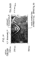
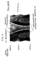
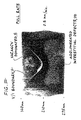
- Agglomerated defects may be detected by a number of different techniques. For example, flow pattern defects, or D-defects, are typically detected by preferentially etching the single crystal silicon sample in a Secco etch solution for about 30 minutes, and then subjecting the sample to microscopic inspection. (See, e.g., H. Yamagishi et al., Semicond. Sci. Technol. 7, A135 (1992).) Although standard for the detection of agglomerated vacancy defects, this process may also be used to detect agglomerated interstitial defects. When this technique is used, such defects appear as large pits on the surface of the sample when present.
- Agglomerated defects may also be detected using laser scattering techniques, such as laser scattering tomography, which typically have a lower defect density detection limit that other etching techniques.
- agglomerated intrinsic point defects may be visually detected by decorating these defects with a metal capable of diffusing into the single crystal silicon matrix upon the application of heat.
- single crystal silicon samples such as wafers, slugs or slabs, may be visually inspected for the presence of such defects by first coating a surface of the sample with a composition containing a metal capable of decorating these defects, such as a concentrated solution of copper nitrate. The coated sample is then heated to a temperature between about 900°C and about 1000°C for about 5 minutes to about 15 minutes in order to diffuse the metal into the sample. The heat treated sample is then cooled to room temperature, thus causing the metal to become critically supersaturated and precipitate at sites within the sample matrix at which defects are present.
- the sample is then rinsed with deionized water and subjected to a second etching step by immersing the sample in, or treating it with, a Secco or Wright etch solution for about 35 -to about 55 minutes.
- a Secco or Wright etch solution comprising about a 1:2 ratio of 0.15 M potassium dichromate and hydrofluoric acid (49% solution by weight). This etching step acts to reveal, or delineate, agglomerated defects which may be present.
- agglomerated intrinsic point defects mean defects caused (i) by the reaction in which vacancies agglomerate to produce D-defects, flow pattern defects, gate oxide integrity defects, crystal originated particle defects, crystal originated light point defects, and other such vacancy related defects, or (ii) by the reaction in which self-interstitials agglomerate to produce dislocation loops and networks, and other such self-interstitial related defects;
- agglomerated interstitial defects shall mean agglomerated intrinsic point defects caused by the reaction in which silicon self-interstitial atoms agglomerate;
- agglomerated vacancy defects shall mean agglomerated vacancy point defects caused by the reaction in which crystal lattice vacancies agglomerate;
- radius means the distance measured from a central axis to a circumferential edge of a wafer or ingot;
- substantially free of agglomerated intrinsic point defects shall mean a concentration of a
- Examples 1 through 7 illustrate the preparation of a single crystal silicon ingot, from which a wafer may be obtained, the wafering being suitable for thermal annealing in accordance with the present invention; that is, these Examples illustrate that a single crystal silicon wafer may be prepared having a substantially defect free axially symmetric region of interstitial dominated material surrounding a core of vacancy dominated material.
- Example 8 illustrates the effect thermal annealing has on agglomerated vacancy defects, present in the core of such a wafer.
- a first 200 mm single crystal silicon ingot was grown under conditions in which the pull rate was ramped linearly from about 0.75 mm/min. to about 0.35 mm/min. over the length of the crystal.
- Fig. 7 shows the pull rate as a function of crystal length.
- the width of the axially symmetric region 6 (a region which is interstitial dominated material but which lacks agglomerated interstitial defects) is at its maximum; the width of the vacancy dominated region 8, R V *(680) is about 35 mm and the width of the axially symmetric region, R I *(680) is about 65 mm.
- Fig. 9 shows the pull rate as a function of crystal length for each of the four crystals, labeled, respectively, as 1-4. These four crystals were then analyzed to determine the axial position (and corresponding pull rate) at which agglomerated interstitial defects first appear or disappear. These four empirically determined points (marked "*") are shown in Fig. 9. Interpolation between and extrapolation from these points yielded a curve, labeled v*(Z) in Fig. 9. This curve represents, to a first approximation, the pull rate for 200 mm crystals as a function of length in the crystal puller at which the axially symmetric region is at its maximum width.
- Figs. 10 and 11 illustrate the improvement in quality that can be achieved by reduction of the radial variation in the axial temperature gradient at the melt/solid interface, G 0 (r).
- the pull rate was adjusted such that the boundary between vacancy-rich silicon and interstitial-rich silicon is at a radius of 3 cm.
- the pull rates used for case 1 and 2 were 0.4 and 0.35 mm/min, respectively. From Fig.
- Figs. 12 and 13 illustrate the improvement in quality that can be achieved by increasing the time for out-diffusion of interstitials.
- the concentration of interstitials is calculated for two cases with differing axial temperature profiles in the crystal, dT/dz.
- the axial temperature gradient at the melt/solid interface is the same for both cases, so that the initial concentration (about 1 cm from the melt/solid interface) of interstitials is the same for both cases.
- the pull rate was adjusted such that the entire crystal is interstitial-rich.
- the pull rate was the same for both cases, 0.32 mm/min.
- the longer time for interstitial out-diffusion in case 2 results in an overall reduction of the interstitial concentration. This leads to an improvement in the quality of the material since it becomes easier to avoid the formation of interstitial defect clusters due to supersaturation of interstitials.
- a 700 mm long, 150 mm diameter crystal was grown with a varying pull rate.
- the pull rate varied nearly linearly from about 1.2 mm/min at the shoulder to about 0.4 mm/min at 430 mm from the shoulder, and then nearly linearly back to about 0.65 mm/min at 700 mm from the shoulder.
- the entire radius is grown under interstitial-rich conditions over the length of crystal ranging from about 320 mm to about 525 mm from the shoulder of the crystal.
- the crystal is free of agglomerated intrinsic point defects clusters across the entire diameter. Stated another way, there is one small section of the crystal in which the width of the axially symmetric region, i.e., the region which is substantially free of agglomerated defects, is equal to the radius of the ingot.
- Example 1 a series of single crystal silicon ingots were grown at varying pull rates and then analyzed to determine the axial position (and corresponding pull rate) at which agglomerated interstitial defects first appeared or disappeared. Interpolation between and extrapolation from these points, plotted on a graph of pull rate v. axial position, yielded a curve which represents, to a first approximation, the pull rate for a 200 mm crystal as a function of length in the crystal puller at which the axially symmetric region is at its maximum width. Additional crystals were then grown at other pull rates and further analysis of these crystals was used to refine this empirically determined optimum pull rate profile.
- a crystal of about 1000 mm in length and about 200 mm in diameter was grown.
- Slices of the grown crystal, obtained from various axial position, were then analyzed using oxygen precipitation methods standard in the art in order to (i) determine if agglomerated interstitial defects were formed, and (ii) determine, as a function of the radius of the slice, the position of the V/I boundary. In this way the presence of an axially symmetric region was determined, as well as the width of this region a function of crystal length or position.
- a single crystal silicon ingot having a length of about 1100 mm and a diameter of about 150 mm was grown with a decreasing pull rate.
- the pull rate at the shoulder of the constant diameter portion of the ingot was about 1 mm/min.
- the pull rate decreased exponentially to about 0.4 mm/min., which corresponded to an axial position of about 200 mm from the shoulder.
- the pull rate then decreased linearly until a rate of about 0.3 mm/min. was reached near the end of the constant diameter portion of the ingot.
- a series of single crystal silicon ingots (150 mm and 200 mm nominal diameters), were grown in accordance with the Czochralski method using different hot zone configurations, designed by means common in the art, which affected the residence time of the silicon at temperatures in excess of about 1050°C.
- the pull rate profile for each ingot was varied along the length of the ingot in an attempt to create a transition from a region of agglomerated vacancy point defects to a region of agglomerated interstitial point defects.
- the ingots were cut longitudinally along the central axis running parallel to the direction of growth, and then further divided into sections which were each about 2 mm in thickness.
- one set of such longitudinal sections was then heated and intentionally contaminated with copper, the heating conditions being appropriate for the dissolution of a high concentration of copper interstitials.
- the samples were then rapidly cooled, during which time the copper impurities either outdiffused or precipitated at sites where oxide clusters or agglomerated interstitial defects where present.
- the samples were visually inspected for the presence of precipitated impurities; those regions which were free of such precipitated impurities corresponded to regions which were free of agglomerated interstitial defects.
- Another set of the longitudinal sections was subjected to a series of oxygen precipitation heat treatments in order to cause the nucleation and growth of new oxide clusters prior to carrier lifetime mapping. Contrast bands in lifetime mapping were utilized in order to determine and measure the shape of the instantaneous melt/solid interface at various axial positions in each ingot. Information on the shape of the melt/solid interface was then used, as discussed further below, to estimate the absolute value of, and the radial variation in, the average axial temperature gradient, G 0 . This information was also used, in conjunction with the pull rate, to estimate the radial variation in v/G 0 .
- the second assumption that was made to parameterize the effect of growth conditions on the quality of single crystal silicon is that the temperature dependence of silicon self-interstitial diffusivity is negligible. Stated another way, it is assumed that self-interstitials diffuse at the same rate at all temperatures between about 1400°C and about 1050°C. Understanding that about 1050°C is considered a reasonable approximation for the temperature of agglomeration, the essential point of this assumption is that the details of the cooling curve from the melting point does not matter. The diffusion distance depends only on the total time spent cooling from the melting point to about 1050°C.
- the total cooling time from about 1400°C to about 1050°C may be calculated. It should be noted that the rate at which the temperature changes for each of the hot zones was reasonably uniform. This uniformity means that any error in the selection of a temperature of nucleation for agglomerated interstitial defects, i.e., about 1050°C, will ideally lead only to scaled errors in the calculated cooling time.
- the width of the axially symmetric region was generally assumed to be based on the position of the V/I boundary after cooling to room temperature. This is pointed out because, as mentioned above, as the ingot cools recombination of vacancies and silicon self-interstitials may occur. When recombination does occur, the actual position of the V/I boundary shifts inwardly toward the central axis of the ingot. It is this final position which is being referred to here.
- the melt/solid interface shape was assumed to be the melting point isotherm.
- the crystal surface temperatures were calculated using finite element modeling (FEA) techniques and the details of the hot zone design.
- FEA finite element modeling
- the entire temperature field within the crystal, and therefore G 0 was deduced by solving Laplace's equation with the proper boundary conditions, namely, the melting point along the melt/solid interface and the FEA results for the surface temperature along the axis of the crystal.
- the results obtained at various axial positions from one of the ingots prepared and evaluated are presented in Fig. 17.
- a radial position R' that is, a position halfway between the V/I boundary and the crystal surface, was assumed to be the furthest point a silicon self-interstitial can be from a sink in the ingot, whether that sink be in the vacancy dominated region or on the crystal surface.
- the difference between the calculated v/G 0 at the position R' and v/G 0 at the V/I boundary i.e., the critical v/G 0 value
- the critical v/G 0 value provides an indication of the radial variation in the initial interstitial concentration, as well as the effect this has on the ability for excess interstitials to reach a sink on the crystal surface or in the vacancy dominated region.
- a correlation may be made between the quality of the sample and the width of the axially symmetric region.
- a graph may be prepared which compares the quality of the given sample to the time the sample, at that particular axial position, was allowed to cool from solidification to about 1050°C.
- this graph shows the width of the axially symmetric region (i.e., R crystal - R vacancy ) has a strong dependence on the cooling history of the sample within this particular temperature range.
- the width of the axially symmetric region i.e., R crystal - R vacancy
- a best fit line may be calculated which generally represents a transition in the quality of the silicon from "good” (i.e., defect-free) to "bad” (i.e., containing defects), as a function of the cooling time allowed for a given ingot diameter within this particular temperature range.
- cooling times of about 65 to about 75 hours may be needed in order to obtain an axially symmetric region having a width about equal to the radius of an ingot having a diameter of about 300 mm. It is to be noted in this regard that, as the diameter of the ingot increases, additional cooling time is required due to the increase in distance that interstitials must diffuse in order to reach sinks at the ingot surface or the vacancy core.
- FIGs. 20, 21, 22 and 23 the effects of increased cooling time for various ingots may be observed.
- Each of these figures depicts a portion of an ingot having a nominal diameter of 200 mm, with the cooling time from the temperature of solidification to 1050 °C progressively increasing from Fig. 20 to Fig. 23.
- the width of the axially symmetric region free of agglomerated interstitial defects is at a maximum, which is about 45% of the radius of the ingot.
- a transition occurs from a region which is free of such defects, to a region in which such defects are present.
- FIG. 21 a portion of an ingot, ranging in axial position from about 305 mm to about 460 mm from the shoulder, is shown.
- the width of the axially symmetric region free of agglomerated interstitial defects is at a maximum, which is about 65% of the radius of the ingot. Beyond this position, defect formation begins.
- the width of the axially symmetric region is about equal to the radius of the ingot; that is, a small portion of the ingot within this range is free of agglomerated intrinsic point defects.
- Figs. 20, 21, 22, and 23 demonstrate the effect of cooling time to 1050 °C upon the width and the length of the defect-free, axially symmetric region.
- the regions containing agglomerated interstitial defects occurred as a result of a continued decrease of the crystal pull rate leading to an initial interstitial concentration which was too large to reduce for the cooling time of that portion of the crystal.
- a greater length of the axially symmetric region means a larger range of pull rates (i.e., initial interstitial concentration) are available for the growth of such defect-free material.
- a region of vacancy dominated material free of agglomerated defects is present in which the width of the region is equal to the radius of the ingot.
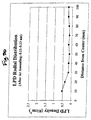
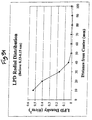
- a number of 200 mm wafers obtained from the process of the present invention where analyzed by laser beam surface scanning equipment common in the art (see, e.g., Tencor SP1 laser scanner, commercially available from Tencor Inc. of Mountain View, California) in order to determine the average number of light point defects (LPDs), including agglomerated vacancy defects, having a size greater than about 0.09 microns, present per square centimeter on the surface of the wafers.
- LPDs light point defects
- the results of the analyses are presented as a function of the distance from the central axis of the wafers.
- the wafers were then thermally annealed, the wafers being heated to about 1200°C for about 2 hours.
- the wafers were then analyzed by the same method once again.
- the wafers initially contained an average of about 5 LPDs/cm 2 (light point defects per square centimeter) to about 0.2 LPD/cm 2 over a distance of about 50 mm from the central axis, the number decreasing as the distance from the central axis increases.
- the wafers contained an average of about 1 LPD/cm 2 to about 0.2 LPD/cm 2 within the same region.
- the results clearly show that within the axially symmetric region of the vacancy-type material, agglomerated vacancy defects were dissolved or reduced in size as a result of the thermal anneal.
- the size of the defects were reduced below 0.09 microns (i.e., the lower limit of the defect size being detected), effectively causing the number of defects within this size range to be reduced by about 80% (i.e., the number density was reduced by about 80%).
- the initial and final results of the surface analyses are further divided by defect size. It may first be observed that the thermal anneal is successful in dissolving or reducing in size agglomerated vacancy defects ranging in size from about 0.09 microns up to about 0.15 microns. It may further be observed from these results that the majority of the LPDs detected were small, ranging in size from about 0.09 microns up to about 0.13 microns. Without being held to any particular theory, this is believed to be the case because the width of the vacancy core is generally small, extending over only about 50% of the radius.
- the width of the axially symmetric region substantially free of agglomerated interstitial defects is at least about 50% of the radius of the wafer, in order to ensure agglomerated vacancy defects (if present) are more easily dissolved; that is, preferably the width of the vacancy core will be less than about 50% of the radius of the wafer.
- Figs. 33a through 33b it may be observed that when the single crystal silicon material is grown to be vacancy-dominated from center to edge (denoted "case I”; see Figs. 33a and 33b), the resulting vacancy concentration in the material is very high, as compared to material prepared in accordance with the present invention (denoted "case II”; see Figs. 33a and 33c). Material prepared by the present process to have a vacancy core of minimal width has a much lower concentration of vacancy intrinsic point defects and, therefore, the resulting size of the agglomerated defects, if formed, are much smaller. As can be seen from Figs. 27 through 30, smaller defects are more easily dissolved.
Applications Claiming Priority (3)
| Application Number | Priority Date | Filing Date | Title |
|---|---|---|---|
| US10430498P | 1998-10-14 | 1998-10-14 | |
| US104304P | 1998-10-14 | ||
| PCT/US1999/024068 WO2000022198A1 (en) | 1998-10-14 | 1999-10-13 | Thermally annealed, low defect density single crystal silicon |
Publications (2)
| Publication Number | Publication Date |
|---|---|
| EP1125008A1 EP1125008A1 (en) | 2001-08-22 |
| EP1125008B1 true EP1125008B1 (en) | 2003-06-18 |
Family
ID=22299774
Family Applications (1)
| Application Number | Title | Priority Date | Filing Date |
|---|---|---|---|
| EP99956562A Expired - Lifetime EP1125008B1 (en) | 1998-10-14 | 1999-10-13 | Thermally annealed, low defect density single crystal silicon |
Country Status (8)
| Country | Link |
|---|---|
| US (2) | US6416836B1 (zh) |
| EP (1) | EP1125008B1 (zh) |
| JP (1) | JP4875800B2 (zh) |
| KR (1) | KR100622884B1 (zh) |
| CN (1) | CN1296526C (zh) |
| DE (1) | DE69908965T2 (zh) |
| TW (1) | TW467974B (zh) |
| WO (1) | WO2000022198A1 (zh) |
Cited By (1)
| Publication number | Priority date | Publication date | Assignee | Title |
|---|---|---|---|---|
| US7387676B2 (en) | 2005-06-17 | 2008-06-17 | Siltronic Ag | Process for producing silicon semiconductor wafers with defined defect properties, and silicon semiconductor wafers having these defect properties |
Families Citing this family (23)
| Publication number | Priority date | Publication date | Assignee | Title |
|---|---|---|---|---|
| US6503594B2 (en) | 1997-02-13 | 2003-01-07 | Samsung Electronics Co., Ltd. | Silicon wafers having controlled distribution of defects and slip |
| SG165151A1 (en) * | 1997-04-09 | 2010-10-28 | Memc Electronic Materials | Low defect density silicon |
| KR100378184B1 (ko) * | 1999-11-13 | 2003-03-29 | 삼성전자주식회사 | 제어된 결함 분포를 갖는 실리콘 웨이퍼, 그의 제조공정및 단결정 실리콘 잉곳의 제조를 위한 초크랄스키 풀러 |
| US6444027B1 (en) | 2000-05-08 | 2002-09-03 | Memc Electronic Materials, Inc. | Modified susceptor for use in chemical vapor deposition process |
| CN1312326C (zh) * | 2000-05-08 | 2007-04-25 | Memc电子材料有限公司 | 消除自动掺杂和背面晕圈的外延硅晶片 |
| DE60127252T2 (de) * | 2000-05-08 | 2007-12-20 | Memc Electronic Materials, Inc. | Epitaktischer siliziumwafer frei von selbstdotierung und rückseitenhalo |
| US7008874B2 (en) * | 2000-12-19 | 2006-03-07 | Memc Electronics Materials, Inc. | Process for reclaiming semiconductor wafers and reclaimed wafers |
| KR100805518B1 (ko) | 2001-01-26 | 2008-02-20 | 엠이엠씨 일렉트로닉 머티리얼즈 인코포레이티드 | 산화 유도된 적층 결함을 실질적으로 포함하지 않는베이컨시 지배 코어를 갖는 낮은 결함 밀도의 실리콘 |
| WO2003001583A2 (en) * | 2001-06-22 | 2003-01-03 | Memc Electronic Materials, Inc. | Process for producing silicon on insulator structure having intrinsic gettering by ion implantation |
| JP3778432B2 (ja) * | 2002-01-23 | 2006-05-24 | 東京エレクトロン株式会社 | 基板処理方法および装置、半導体装置の製造装置 |
| KR100588425B1 (ko) * | 2003-03-27 | 2006-06-12 | 실트로닉 아게 | 실리콘 단결정, 결정된 결함분포를 가진 실리콘 단결정 및 실리콘 반도체 웨이퍼의 제조방법 |
| US7135631B2 (en) * | 2004-01-12 | 2006-11-14 | Cherny Michale N | Quartz drum and method of making |
| US7067005B2 (en) * | 2004-08-06 | 2006-06-27 | Sumitomo Mitsubishi Silicon Corporation | Silicon wafer production process and silicon wafer |
| WO2007130708A1 (en) * | 2006-01-30 | 2007-11-15 | Memc Electronic Materials, Inc. | Double side wafer grinder and methods for assessing workpiece nanotopology |
| KR101385810B1 (ko) | 2006-05-19 | 2014-04-16 | 엠이엠씨 일렉트로닉 머티리얼즈, 인크. | Cz 성장 동안에 실리콘 단결정의 측면에 의해 유도되는 응집된 점 결함 및 산소 클러스터 형성을 제어하는 방법 |
| US20070299162A1 (en) * | 2006-06-27 | 2007-12-27 | Gelcore Llc | Optoelectronic device |
| JP5311930B2 (ja) * | 2007-08-29 | 2013-10-09 | 住友化学株式会社 | シリコンの製造方法 |
| KR100901980B1 (ko) * | 2007-09-04 | 2009-06-08 | 주식회사 실트론 | 플로팅 존 공정을 이용한 웨이퍼 표면 처리방법 및 이를위한 웨이퍼 표면 처리장치 |
| EP2309038B1 (en) * | 2009-10-08 | 2013-01-02 | Siltronic AG | production method of an epitaxial wafer |
| CN103835000A (zh) * | 2012-11-20 | 2014-06-04 | 上海华虹宏力半导体制造有限公司 | 一种高温改善多晶硅表面粗糙度的方法 |
| CN106206275A (zh) * | 2016-09-20 | 2016-12-07 | 上海华力微电子有限公司 | 一种改善多晶硅表面粗糙度的工艺方法 |
| CN108169228A (zh) * | 2017-11-28 | 2018-06-15 | 中国工程物理研究院电子工程研究所 | 一种准确辨别碳化硅单晶位错类型的方法 |
| WO2019125810A1 (en) * | 2017-12-21 | 2019-06-27 | Globalwafers Co., Ltd. | Method of treating a single crystal silicon ingot to improve the lls ring/core pattern |
Family Cites Families (87)
| Publication number | Priority date | Publication date | Assignee | Title |
|---|---|---|---|---|
| JPS583375B2 (ja) | 1979-01-19 | 1983-01-21 | 超エル・エス・アイ技術研究組合 | シリコン単結晶ウエハ−の製造方法 |
| JPS5680139A (en) | 1979-12-05 | 1981-07-01 | Chiyou Lsi Gijutsu Kenkyu Kumiai | Manufacture of semiconductor device |
| US4437922A (en) | 1982-03-26 | 1984-03-20 | International Business Machines Corporation | Method for tailoring oxygen precipitate particle density and distribution silicon wafers |
| JPS59190300A (ja) | 1983-04-08 | 1984-10-29 | Hitachi Ltd | 半導体製造方法および装置 |
| US4549654A (en) * | 1983-05-31 | 1985-10-29 | Champion International Corporation | Article display package and blank therefor |
| US4548654A (en) | 1983-06-03 | 1985-10-22 | Motorola, Inc. | Surface denuding of silicon wafer |
| US4505759A (en) | 1983-12-19 | 1985-03-19 | Mara William C O | Method for making a conductive silicon substrate by heat treatment of oxygenated and lightly doped silicon single crystals |
| JPS62105998A (ja) | 1985-10-31 | 1987-05-16 | Sony Corp | シリコン基板の製法 |
| US4868133A (en) | 1988-02-11 | 1989-09-19 | Dns Electronic Materials, Inc. | Semiconductor wafer fabrication with improved control of internal gettering sites using RTA |
| US4851358A (en) | 1988-02-11 | 1989-07-25 | Dns Electronic Materials, Inc. | Semiconductor wafer fabrication with improved control of internal gettering sites using rapid thermal annealing |
| US5264189A (en) | 1988-02-23 | 1993-11-23 | Mitsubishi Materials Corporation | Apparatus for growing silicon crystals |
| US4981549A (en) | 1988-02-23 | 1991-01-01 | Mitsubishi Kinzoku Kabushiki Kaisha | Method and apparatus for growing silicon crystals |
| JPH02180789A (ja) | 1989-01-05 | 1990-07-13 | Kawasaki Steel Corp | Si単結晶の製造方法 |
| JPH0633236B2 (ja) | 1989-09-04 | 1994-05-02 | 新日本製鐵株式会社 | シリコン単結晶の熱処理方法および装置ならびに製造装置 |
| JPH04108682A (ja) | 1990-08-30 | 1992-04-09 | Fuji Electric Co Ltd | 化合物半導体単結晶製造装置および製造方法 |
| JPH0750713B2 (ja) * | 1990-09-21 | 1995-05-31 | コマツ電子金属株式会社 | 半導体ウェーハの熱処理方法 |
| IT1242014B (it) | 1990-11-15 | 1994-02-02 | Memc Electronic Materials | Procedimento per il trattamento di fette di silicio per ottenere in esse profili di precipitazione controllati per la produzione di componenti elettronici. |
| JP2613498B2 (ja) | 1991-03-15 | 1997-05-28 | 信越半導体株式会社 | Si単結晶ウエーハの熱処理方法 |
| JP3016897B2 (ja) | 1991-03-20 | 2000-03-06 | 信越半導体株式会社 | シリコン単結晶の製造方法及び装置 |
| JP2758093B2 (ja) | 1991-10-07 | 1998-05-25 | 信越半導体株式会社 | 半導体ウェーハの製造方法 |
| JP2726583B2 (ja) | 1991-11-18 | 1998-03-11 | 三菱マテリアルシリコン株式会社 | 半導体基板 |
| JPH0684925A (ja) | 1992-07-17 | 1994-03-25 | Toshiba Corp | 半導体基板およびその処理方法 |
| WO1994016124A1 (fr) | 1993-01-06 | 1994-07-21 | Nippon Steel Corporation | Procede et appareil pour prevoir la qualite du cristal d'un semi-conducteur monocristallin |
| KR0139730B1 (ko) | 1993-02-23 | 1998-06-01 | 사또오 후미오 | 반도체 기판 및 그 제조방법 |
| US5401669A (en) | 1993-05-13 | 1995-03-28 | Memc Electronic Materials, Spa | Process for the preparation of silicon wafers having controlled distribution of oxygen precipitate nucleation centers |
| JPH0786289A (ja) | 1993-07-22 | 1995-03-31 | Toshiba Corp | 半導体シリコンウェハおよびその製造方法 |
| JPH0741383A (ja) | 1993-07-29 | 1995-02-10 | Nippon Steel Corp | 半導体単結晶およびその製造方法 |
| IT1280041B1 (it) | 1993-12-16 | 1997-12-29 | Wacker Chemitronic | Procedimento per il tiraggio di un monocristallo di silicio |
| DE4414947C2 (de) | 1993-12-16 | 1998-12-17 | Wacker Siltronic Halbleitermat | Verfahren zum Ziehen eines Einkristalls aus Silicium |
| JP3276500B2 (ja) | 1994-01-14 | 2002-04-22 | ワッカー・エヌエスシーイー株式会社 | シリコンウェーハとその製造方法 |
| US5445975A (en) | 1994-03-07 | 1995-08-29 | Advanced Micro Devices, Inc. | Semiconductor wafer with enhanced pre-process denudation and process-induced gettering |
| US5474020A (en) | 1994-05-06 | 1995-12-12 | Texas Instruments Incorporated | Oxygen precipitation control in czochralski-grown silicon cyrstals |
| JPH07321120A (ja) | 1994-05-25 | 1995-12-08 | Komatsu Electron Metals Co Ltd | シリコンウェーハの熱処理方法 |
| JP3458342B2 (ja) | 1994-06-03 | 2003-10-20 | コマツ電子金属株式会社 | シリコンウェーハの製造方法およびシリコンウェーハ |
| JP2874834B2 (ja) | 1994-07-29 | 1999-03-24 | 三菱マテリアル株式会社 | シリコンウェーハのイントリンシックゲッタリング処理法 |
| JPH0845944A (ja) | 1994-07-29 | 1996-02-16 | Sumitomo Sitix Corp | シリコンウェーハの製造方法 |
| JPH0845947A (ja) | 1994-08-03 | 1996-02-16 | Nippon Steel Corp | シリコン基板の熱処理方法 |
| JPH08115919A (ja) * | 1994-10-18 | 1996-05-07 | Toshiba Corp | 半導体基板の処理方法 |
| JP3285111B2 (ja) | 1994-12-05 | 2002-05-27 | 信越半導体株式会社 | 結晶欠陥の少ないシリコン単結晶の製造方法 |
| JPH08208374A (ja) | 1995-01-25 | 1996-08-13 | Nippon Steel Corp | シリコン単結晶およびその製造方法 |
| US5611855A (en) | 1995-01-31 | 1997-03-18 | Seh America, Inc. | Method for manufacturing a calibration wafer having a microdefect-free layer of a precisely predetermined depth |
| US5788763A (en) | 1995-03-09 | 1998-08-04 | Toshiba Ceramics Co., Ltd. | Manufacturing method of a silicon wafer having a controlled BMD concentration |
| US5593494A (en) | 1995-03-14 | 1997-01-14 | Memc Electronic Materials, Inc. | Precision controlled precipitation of oxygen in silicon |
| JP2826589B2 (ja) | 1995-03-30 | 1998-11-18 | 住友シチックス株式会社 | 単結晶シリコン育成方法 |
| JP3085146B2 (ja) | 1995-05-31 | 2000-09-04 | 住友金属工業株式会社 | シリコン単結晶ウェーハおよびその製造方法 |
| JPH08337490A (ja) | 1995-06-09 | 1996-12-24 | Shin Etsu Handotai Co Ltd | 結晶欠陥の少ないシリコン単結晶及びその製造方法 |
| JP3006669B2 (ja) | 1995-06-20 | 2000-02-07 | 信越半導体株式会社 | 結晶欠陥の均一なシリコン単結晶の製造方法およびその製造装置 |
| JP3381816B2 (ja) | 1996-01-17 | 2003-03-04 | 三菱住友シリコン株式会社 | 半導体基板の製造方法 |
| JP4020987B2 (ja) | 1996-01-19 | 2007-12-12 | 信越半導体株式会社 | ウエーハ周辺部に結晶欠陥がないシリコン単結晶およびその製造方法 |
| DE19613282A1 (de) | 1996-04-03 | 1997-10-09 | Leybold Ag | Vorrichtung zum Ziehen von Einkristallen |
| DE19637182A1 (de) * | 1996-09-12 | 1998-03-19 | Wacker Siltronic Halbleitermat | Verfahren zur Herstellung von Halbleiterscheiben aus Silicium mit geringer Defektdichte |
| JPH10152395A (ja) | 1996-11-21 | 1998-06-09 | Komatsu Electron Metals Co Ltd | シリコン単結晶の製造方法 |
| JPH10154713A (ja) * | 1996-11-22 | 1998-06-09 | Shin Etsu Handotai Co Ltd | シリコンウエーハの熱処理方法およびシリコンウエーハ |
| US5868710A (en) * | 1996-11-22 | 1999-02-09 | Liebel Flarsheim Company | Medical fluid injector |
| KR100240023B1 (ko) | 1996-11-29 | 2000-01-15 | 윤종용 | 반도체 웨이퍼 열처리방법 및 이에 따라 형성된 반도체 웨이퍼 |
| JP4041182B2 (ja) * | 1997-01-27 | 2008-01-30 | Sumco Techxiv株式会社 | 熱処理用シリコンウェーハ及びその製造方法 |
| SG64470A1 (en) * | 1997-02-13 | 1999-04-27 | Samsung Electronics Co Ltd | Methods of manufacturing monocrystalline silicon ingots and wafers by controlling pull rate profiles in a hot zone furnace and ingots and wafers manufactured thereby |
| US6045610A (en) | 1997-02-13 | 2000-04-04 | Samsung Electronics Co., Ltd. | Methods of manufacturing monocrystalline silicon ingots and wafers by controlling pull rate profiles in a hot zone furnance |
| US5994761A (en) * | 1997-02-26 | 1999-11-30 | Memc Electronic Materials Spa | Ideal oxygen precipitating silicon wafers and oxygen out-diffusion-less process therefor |
| DE19711922A1 (de) | 1997-03-21 | 1998-09-24 | Wacker Siltronic Halbleitermat | Vorrichtung und Verfahren zum Ziehen eines Einkristalls |
| US6403502B1 (en) * | 1997-03-27 | 2002-06-11 | Shin-Etsu Handotai Co., Ltd. | Heat treatment method for a silicon wafer and a silicon wafer heat-treated by the method |
| SG165151A1 (en) | 1997-04-09 | 2010-10-28 | Memc Electronic Materials | Low defect density silicon |
| EP1146150B1 (en) | 1997-04-09 | 2010-06-09 | MEMC Electronic Materials, Inc. | Low defect density, ideal oxygen precipitating silicon |
| JPH1179889A (ja) | 1997-07-09 | 1999-03-23 | Shin Etsu Handotai Co Ltd | 結晶欠陥が少ないシリコン単結晶の製造方法、製造装置並びにこの方法、装置で製造されたシリコン単結晶とシリコンウエーハ |
| US5942032A (en) | 1997-08-01 | 1999-08-24 | Memc Electronic Materials, Inc. | Heat shield assembly and method of growing vacancy rich single crystal silicon |
| TW429478B (en) | 1997-08-29 | 2001-04-11 | Toshiba Corp | Semiconductor device and method for manufacturing the same |
| US5922127A (en) | 1997-09-30 | 1999-07-13 | Memc Electronic Materials, Inc. | Heat shield for crystal puller |
| JP3919308B2 (ja) | 1997-10-17 | 2007-05-23 | 信越半導体株式会社 | 結晶欠陥の少ないシリコン単結晶の製造方法ならびにこの方法で製造されたシリコン単結晶およびシリコンウエーハ |
| JP3451908B2 (ja) * | 1997-11-05 | 2003-09-29 | 信越半導体株式会社 | Soiウエーハの熱処理方法およびsoiウエーハ |
| JP3446572B2 (ja) * | 1997-11-11 | 2003-09-16 | 信越半導体株式会社 | シリコン単結晶中の酸素析出挙動を割り出す方法、およびシリコン単結晶ウエーハ製造工程の決定方法、並びにプログラムを記録した記録媒体 |
| JPH11150119A (ja) | 1997-11-14 | 1999-06-02 | Sumitomo Sitix Corp | シリコン半導体基板の熱処理方法とその装置 |
| JP3596257B2 (ja) | 1997-11-19 | 2004-12-02 | 三菱住友シリコン株式会社 | シリコン単結晶ウェーハの製造方法 |
| JP3634133B2 (ja) | 1997-12-17 | 2005-03-30 | 信越半導体株式会社 | 結晶欠陥の少ないシリコン単結晶の製造方法及びシリコン単結晶ウエーハ |
| JP4147599B2 (ja) | 1997-12-26 | 2008-09-10 | 株式会社Sumco | シリコン単結晶及びその製造方法 |
| JP3011178B2 (ja) * | 1998-01-06 | 2000-02-21 | 住友金属工業株式会社 | 半導体シリコンウェーハ並びにその製造方法と熱処理装置 |
| JP3955375B2 (ja) | 1998-01-19 | 2007-08-08 | 信越半導体株式会社 | シリコン単結晶の製造方法およびシリコン単結晶ウエーハ |
| JP3627498B2 (ja) | 1998-01-19 | 2005-03-09 | 信越半導体株式会社 | シリコン単結晶の製造方法 |
| TW508378B (en) * | 1998-03-09 | 2002-11-01 | Shinetsu Handotai Kk | A method for producing a silicon single crystal wafer and a silicon single crystal wafer |
| TW589415B (en) * | 1998-03-09 | 2004-06-01 | Shinetsu Handotai Kk | Method for producing silicon single crystal wafer and silicon single crystal wafer |
| DE19823962A1 (de) | 1998-05-28 | 1999-12-02 | Wacker Siltronic Halbleitermat | Verfahren zur Herstellung eines Einkristalls |
| JPH11349393A (ja) | 1998-06-03 | 1999-12-21 | Shin Etsu Handotai Co Ltd | シリコン単結晶ウエーハおよびシリコン単結晶ウエーハの製造方法 |
| US6077343A (en) * | 1998-06-04 | 2000-06-20 | Shin-Etsu Handotai Co., Ltd. | Silicon single crystal wafer having few defects wherein nitrogen is doped and a method for producing it |
| US6093913A (en) | 1998-06-05 | 2000-07-25 | Memc Electronic Materials, Inc | Electrical heater for crystal growth apparatus with upper sections producing increased heating power compared to lower sections |
| JP3746153B2 (ja) * | 1998-06-09 | 2006-02-15 | 信越半導体株式会社 | シリコンウエーハの熱処理方法 |
| EP1035235A4 (en) * | 1998-08-31 | 2002-05-15 | Shinetsu Handotai Kk | METHOD FOR PRODUCING SILICON SINGLE CRYSTAL WAFERS AND SILICON SINGLE CRYSTAL WAFERS |
| CN1155074C (zh) * | 1998-09-02 | 2004-06-23 | Memc电子材料有限公司 | 从低缺陷密度的单晶硅上制备硅-绝缘体结构 |
| JP3601324B2 (ja) * | 1998-11-19 | 2004-12-15 | 信越半導体株式会社 | 結晶欠陥の少ないシリコン単結晶ウエーハ及びその製造方法 |
-
1999
- 1999-10-13 EP EP99956562A patent/EP1125008B1/en not_active Expired - Lifetime
- 1999-10-13 US US09/416,998 patent/US6416836B1/en not_active Expired - Lifetime
- 1999-10-13 KR KR1020017004280A patent/KR100622884B1/ko not_active IP Right Cessation
- 1999-10-13 CN CNB99812088XA patent/CN1296526C/zh not_active Expired - Fee Related
- 1999-10-13 DE DE69908965T patent/DE69908965T2/de not_active Expired - Lifetime
- 1999-10-13 JP JP2000576083A patent/JP4875800B2/ja not_active Expired - Fee Related
- 1999-10-13 WO PCT/US1999/024068 patent/WO2000022198A1/en active IP Right Grant
- 1999-11-22 TW TW088117746A patent/TW467974B/zh not_active IP Right Cessation
-
2002
- 2002-02-11 US US10/073,506 patent/US6743289B2/en not_active Expired - Lifetime
Cited By (1)
| Publication number | Priority date | Publication date | Assignee | Title |
|---|---|---|---|---|
| US7387676B2 (en) | 2005-06-17 | 2008-06-17 | Siltronic Ag | Process for producing silicon semiconductor wafers with defined defect properties, and silicon semiconductor wafers having these defect properties |
Also Published As
| Publication number | Publication date |
|---|---|
| JP4875800B2 (ja) | 2012-02-15 |
| KR100622884B1 (ko) | 2006-09-12 |
| WO2000022198A9 (en) | 2002-08-22 |
| KR20010079992A (ko) | 2001-08-22 |
| WO2000022198A1 (en) | 2000-04-20 |
| US6743289B2 (en) | 2004-06-01 |
| DE69908965D1 (de) | 2003-07-24 |
| US6416836B1 (en) | 2002-07-09 |
| CN1323362A (zh) | 2001-11-21 |
| CN1296526C (zh) | 2007-01-24 |
| US20020083889A1 (en) | 2002-07-04 |
| TW467974B (en) | 2001-12-11 |
| DE69908965T2 (de) | 2004-05-13 |
| EP1125008A1 (en) | 2001-08-22 |
| JP2002527895A (ja) | 2002-08-27 |
Similar Documents
| Publication | Publication Date | Title |
|---|---|---|
| EP1273684B1 (en) | Low defect density, vacancy dominated silicon | |
| EP1125008B1 (en) | Thermally annealed, low defect density single crystal silicon | |
| US20050238905A1 (en) | Vacancy-dominated, defect-free silicon | |
| US7097718B2 (en) | Single crystal silicon wafer having an epitaxial layer substantially free from grown-in defects | |
| US20010045184A1 (en) | Crystal puller for growing low defect density, self-interstitial dominated silicon | |
| US20020084451A1 (en) | Silicon wafers substantially free of oxidation induced stacking faults |
Legal Events
| Date | Code | Title | Description |
|---|---|---|---|
| PUAI | Public reference made under article 153(3) epc to a published international application that has entered the european phase |
Free format text: ORIGINAL CODE: 0009012 |
|
| 17P | Request for examination filed |
Effective date: 20010509 |
|
| AK | Designated contracting states |
Kind code of ref document: A1 Designated state(s): AT BE CH CY DE DK ES FI FR GB GR IE IT LI LU MC NL PT SE |
|
| GRAH | Despatch of communication of intention to grant a patent |
Free format text: ORIGINAL CODE: EPIDOS IGRA |
|
| RAP1 | Party data changed (applicant data changed or rights of an application transferred) |
Owner name: MEMC ELECTRONIC MATERIALS, INC. |
|
| GRAH | Despatch of communication of intention to grant a patent |
Free format text: ORIGINAL CODE: EPIDOS IGRA |
|
| GRAA | (expected) grant |
Free format text: ORIGINAL CODE: 0009210 |
|
| AK | Designated contracting states |
Designated state(s): DE FR GB IT |
|
| REG | Reference to a national code |
Ref country code: GB Ref legal event code: FG4D |
|
| REG | Reference to a national code |
Ref country code: IE Ref legal event code: FG4D |
|
| REF | Corresponds to: |
Ref document number: 69908965 Country of ref document: DE Date of ref document: 20030724 Kind code of ref document: P |
|
| ET | Fr: translation filed | ||
| PLBE | No opposition filed within time limit |
Free format text: ORIGINAL CODE: 0009261 |
|
| STAA | Information on the status of an ep patent application or granted ep patent |
Free format text: STATUS: NO OPPOSITION FILED WITHIN TIME LIMIT |
|
| 26N | No opposition filed |
Effective date: 20040319 |
|
| REG | Reference to a national code |
Ref country code: IE Ref legal event code: MM4A |
|
| PGFP | Annual fee paid to national office [announced via postgrant information from national office to epo] |
Ref country code: GB Payment date: 20101025 Year of fee payment: 12 Ref country code: IT Payment date: 20101027 Year of fee payment: 12 |
|
| GBPC | Gb: european patent ceased through non-payment of renewal fee |
Effective date: 20111013 |
|
| PG25 | Lapsed in a contracting state [announced via postgrant information from national office to epo] |
Ref country code: GB Free format text: LAPSE BECAUSE OF NON-PAYMENT OF DUE FEES Effective date: 20111013 Ref country code: IT Free format text: LAPSE BECAUSE OF NON-PAYMENT OF DUE FEES Effective date: 20111013 |
|
| REG | Reference to a national code |
Ref country code: DE Ref legal event code: R082 Ref document number: 69908965 Country of ref document: DE Representative=s name: MAIWALD PATENTANWALTSGESELLSCHAFT MBH, DE |
|
| PGFP | Annual fee paid to national office [announced via postgrant information from national office to epo] |
Ref country code: DE Payment date: 20131029 Year of fee payment: 15 Ref country code: FR Payment date: 20131017 Year of fee payment: 15 |
|
| REG | Reference to a national code |
Ref country code: DE Ref legal event code: R119 Ref document number: 69908965 Country of ref document: DE |
|
| PG25 | Lapsed in a contracting state [announced via postgrant information from national office to epo] |
Ref country code: DE Free format text: LAPSE BECAUSE OF NON-PAYMENT OF DUE FEES Effective date: 20150501 |
|
| REG | Reference to a national code |
Ref country code: FR Ref legal event code: ST Effective date: 20150630 |
|
| PG25 | Lapsed in a contracting state [announced via postgrant information from national office to epo] |
Ref country code: FR Free format text: LAPSE BECAUSE OF NON-PAYMENT OF DUE FEES Effective date: 20141031 |