EP1093159A1 - Procédé d'encapsulation de composants électroniques - Google Patents
Procédé d'encapsulation de composants électroniques Download PDFInfo
- Publication number
- EP1093159A1 EP1093159A1 EP00402796A EP00402796A EP1093159A1 EP 1093159 A1 EP1093159 A1 EP 1093159A1 EP 00402796 A EP00402796 A EP 00402796A EP 00402796 A EP00402796 A EP 00402796A EP 1093159 A1 EP1093159 A1 EP 1093159A1
- Authority
- EP
- European Patent Office
- Prior art keywords
- film
- face
- deformable
- encapsulation method
- components
- Prior art date
- Legal status (The legal status is an assumption and is not a legal conclusion. Google has not performed a legal analysis and makes no representation as to the accuracy of the status listed.)
- Withdrawn
Links
Images


Classifications
-
- H—ELECTRICITY
- H10—SEMICONDUCTOR DEVICES; ELECTRIC SOLID-STATE DEVICES NOT OTHERWISE PROVIDED FOR
- H10W—GENERIC PACKAGES, INTERCONNECTIONS, CONNECTORS OR OTHER CONSTRUCTIONAL DETAILS OF DEVICES COVERED BY CLASS H10
- H10W74/00—Encapsulations, e.g. protective coatings
- H10W74/01—Manufacture or treatment
- H10W74/014—Manufacture or treatment using batch processing
-
- B—PERFORMING OPERATIONS; TRANSPORTING
- B65—CONVEYING; PACKING; STORING; HANDLING THIN OR FILAMENTARY MATERIAL
- B65B—MACHINES, APPARATUS OR DEVICES FOR, OR METHODS OF, PACKAGING ARTICLES OR MATERIALS; UNPACKING
- B65B11/00—Wrapping, e.g. partially or wholly enclosing, articles or quantities of material, in strips, sheets or blanks, of flexible material
-
- H—ELECTRICITY
- H03—ELECTRONIC CIRCUITRY
- H03H—IMPEDANCE NETWORKS, e.g. RESONANT CIRCUITS; RESONATORS
- H03H3/00—Apparatus or processes specially adapted for the manufacture of impedance networks, resonating circuits, resonators
- H03H3/007—Apparatus or processes specially adapted for the manufacture of impedance networks, resonating circuits, resonators for the manufacture of electromechanical resonators or networks
- H03H3/08—Apparatus or processes specially adapted for the manufacture of impedance networks, resonating circuits, resonators for the manufacture of electromechanical resonators or networks for the manufacture of resonators or networks using surface acoustic waves
-
- H—ELECTRICITY
- H10—SEMICONDUCTOR DEVICES; ELECTRIC SOLID-STATE DEVICES NOT OTHERWISE PROVIDED FOR
- H10W—GENERIC PACKAGES, INTERCONNECTIONS, CONNECTORS OR OTHER CONSTRUCTIONAL DETAILS OF DEVICES COVERED BY CLASS H10
- H10W42/00—Arrangements for protection of devices
- H10W42/20—Arrangements for protection of devices protecting against electromagnetic or particle radiation, e.g. light, X-rays, gamma-rays or electrons
-
- H—ELECTRICITY
- H10—SEMICONDUCTOR DEVICES; ELECTRIC SOLID-STATE DEVICES NOT OTHERWISE PROVIDED FOR
- H10W—GENERIC PACKAGES, INTERCONNECTIONS, CONNECTORS OR OTHER CONSTRUCTIONAL DETAILS OF DEVICES COVERED BY CLASS H10
- H10W42/00—Arrangements for protection of devices
- H10W42/20—Arrangements for protection of devices protecting against electromagnetic or particle radiation, e.g. light, X-rays, gamma-rays or electrons
- H10W42/261—Arrangements for protection of devices protecting against electromagnetic or particle radiation, e.g. light, X-rays, gamma-rays or electrons characterised by their shapes or dispositions
- H10W42/276—Arrangements for protection of devices protecting against electromagnetic or particle radiation, e.g. light, X-rays, gamma-rays or electrons characterised by their shapes or dispositions the arrangements being on an external surface of the package, e.g. on the outer surface of an encapsulation
-
- H—ELECTRICITY
- H10—SEMICONDUCTOR DEVICES; ELECTRIC SOLID-STATE DEVICES NOT OTHERWISE PROVIDED FOR
- H10W—GENERIC PACKAGES, INTERCONNECTIONS, CONNECTORS OR OTHER CONSTRUCTIONAL DETAILS OF DEVICES COVERED BY CLASS H10
- H10W74/00—Encapsulations, e.g. protective coatings
- H10W74/01—Manufacture or treatment
-
- H—ELECTRICITY
- H10—SEMICONDUCTOR DEVICES; ELECTRIC SOLID-STATE DEVICES NOT OTHERWISE PROVIDED FOR
- H10W—GENERIC PACKAGES, INTERCONNECTIONS, CONNECTORS OR OTHER CONSTRUCTIONAL DETAILS OF DEVICES COVERED BY CLASS H10
- H10W74/00—Encapsulations, e.g. protective coatings
- H10W74/10—Encapsulations, e.g. protective coatings characterised by their shape or disposition
- H10W74/111—Encapsulations, e.g. protective coatings characterised by their shape or disposition the semiconductor body being completely enclosed
- H10W74/121—Encapsulations, e.g. protective coatings characterised by their shape or disposition the semiconductor body being completely enclosed by multiple encapsulations, e.g. by a thin protective coating and a thick encapsulation
-
- H—ELECTRICITY
- H10—SEMICONDUCTOR DEVICES; ELECTRIC SOLID-STATE DEVICES NOT OTHERWISE PROVIDED FOR
- H10W—GENERIC PACKAGES, INTERCONNECTIONS, CONNECTORS OR OTHER CONSTRUCTIONAL DETAILS OF DEVICES COVERED BY CLASS H10
- H10W74/00—Encapsulations, e.g. protective coatings
- H10W74/10—Encapsulations, e.g. protective coatings characterised by their shape or disposition
- H10W74/131—Encapsulations, e.g. protective coatings characterised by their shape or disposition the semiconductor body being only partially enclosed
- H10W74/144—Encapsulations, e.g. protective coatings characterised by their shape or disposition the semiconductor body being only partially enclosed the encapsulations comprising foils
-
- H—ELECTRICITY
- H10—SEMICONDUCTOR DEVICES; ELECTRIC SOLID-STATE DEVICES NOT OTHERWISE PROVIDED FOR
- H10W—GENERIC PACKAGES, INTERCONNECTIONS, CONNECTORS OR OTHER CONSTRUCTIONAL DETAILS OF DEVICES COVERED BY CLASS H10
- H10W70/00—Package substrates; Interposers; Redistribution layers [RDL]
- H10W70/60—Insulating or insulated package substrates; Interposers; Redistribution layers
- H10W70/67—Insulating or insulated package substrates; Interposers; Redistribution layers characterised by their insulating layers or insulating parts
- H10W70/68—Shapes or dispositions thereof
- H10W70/681—Shapes or dispositions thereof comprising holes not having chips therein, e.g. for outgassing, underfilling or bond wire passage
-
- H—ELECTRICITY
- H10—SEMICONDUCTOR DEVICES; ELECTRIC SOLID-STATE DEVICES NOT OTHERWISE PROVIDED FOR
- H10W—GENERIC PACKAGES, INTERCONNECTIONS, CONNECTORS OR OTHER CONSTRUCTIONAL DETAILS OF DEVICES COVERED BY CLASS H10
- H10W72/00—Interconnections or connectors in packages
- H10W72/01—Manufacture or treatment
- H10W72/0198—Manufacture or treatment batch processes
-
- H—ELECTRICITY
- H10—SEMICONDUCTOR DEVICES; ELECTRIC SOLID-STATE DEVICES NOT OTHERWISE PROVIDED FOR
- H10W—GENERIC PACKAGES, INTERCONNECTIONS, CONNECTORS OR OTHER CONSTRUCTIONAL DETAILS OF DEVICES COVERED BY CLASS H10
- H10W72/00—Interconnections or connectors in packages
- H10W72/851—Dispositions of multiple connectors or interconnections
- H10W72/874—On different surfaces
- H10W72/877—Bump connectors and die-attach connectors
-
- H—ELECTRICITY
- H10—SEMICONDUCTOR DEVICES; ELECTRIC SOLID-STATE DEVICES NOT OTHERWISE PROVIDED FOR
- H10W—GENERIC PACKAGES, INTERCONNECTIONS, CONNECTORS OR OTHER CONSTRUCTIONAL DETAILS OF DEVICES COVERED BY CLASS H10
- H10W72/00—Interconnections or connectors in packages
- H10W72/90—Bond pads, in general
-
- H—ELECTRICITY
- H10—SEMICONDUCTOR DEVICES; ELECTRIC SOLID-STATE DEVICES NOT OTHERWISE PROVIDED FOR
- H10W—GENERIC PACKAGES, INTERCONNECTIONS, CONNECTORS OR OTHER CONSTRUCTIONAL DETAILS OF DEVICES COVERED BY CLASS H10
- H10W72/00—Interconnections or connectors in packages
- H10W72/90—Bond pads, in general
- H10W72/941—Dispositions of bond pads
- H10W72/9415—Dispositions of bond pads relative to the surface, e.g. recessed, protruding
-
- H—ELECTRICITY
- H10—SEMICONDUCTOR DEVICES; ELECTRIC SOLID-STATE DEVICES NOT OTHERWISE PROVIDED FOR
- H10W—GENERIC PACKAGES, INTERCONNECTIONS, CONNECTORS OR OTHER CONSTRUCTIONAL DETAILS OF DEVICES COVERED BY CLASS H10
- H10W74/00—Encapsulations, e.g. protective coatings
-
- H—ELECTRICITY
- H10—SEMICONDUCTOR DEVICES; ELECTRIC SOLID-STATE DEVICES NOT OTHERWISE PROVIDED FOR
- H10W—GENERIC PACKAGES, INTERCONNECTIONS, CONNECTORS OR OTHER CONSTRUCTIONAL DETAILS OF DEVICES COVERED BY CLASS H10
- H10W90/00—Package configurations
- H10W90/701—Package configurations characterised by the relative positions of pads or connectors relative to package parts
- H10W90/721—Package configurations characterised by the relative positions of pads or connectors relative to package parts of bump connectors
- H10W90/724—Package configurations characterised by the relative positions of pads or connectors relative to package parts of bump connectors between a chip and a stacked insulating package substrate, interposer or RDL
Definitions
- the present invention relates to the encapsulation of components electronics, in particular of components whose surface must be free such surface acoustic wave (SAW) filters, RF components, sensors and more precisely the process for producing such a encapsulation.
- SAW surface acoustic wave
- the conventional methods of protecting the components to surface acoustic waves use ceramic boxes or hermetically sealed metal. However, these methods are expensive. and not very productive, and make the miniaturization of the components difficult.
- CSP assembly technologies for Chip-size or Chip-scale Package i.e. encapsulation at chip size or scale
- CSP assembly technologies allow a high degree of miniaturization.
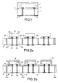
- the one that currently presents the most interest in terms of miniaturization and cost is based on a flip-chip report (technique of the returned chip known to the man of art) as shown in Figure 1.
- a semiconductor component 1 is connected to a base 2 via contacts 11 and 12 of the "flip-chip" type. Electrical pads 21 and 22 allow the whole of the component 1 to external circuits by internal metallizations and through the base. Encapsulation resin 3 consolidates mechanical assembly and ensuring protection of the component.
- the overmolding resin fills the gap between the component and the substrate, which disrupts the propagation of waves surface acoustics.
- the active surface not being passivated unlike semiconductor components, resin alone does not does not constitute a sufficient barrier vis-à-vis external aggressions, such than humidity.
- Hoods can be obtained at from a metal sheet fixed to a weldable frame of the substrate, or a plastic sheet stuck on the substrate between the chips. In the case of a plastic sheet, even metallized, the protection is not airtight neither perfectly armored.
- the present invention proposes to collectively wrap the chips using a deformable plastic film which will adhere on the back and on the sides of the chips as well as on the substrate.
- This process has the advantage of reinforce the mechanical strength of the chip on the substrate. It also the advantage of allowing, after a local film removal step described below, to present a structure on which we can easily make a continuous mineral deposit to make it perfectly waterproof the structure. Finally, if the mineral deposit is chosen to be metallic, a continuous electromagnetic shielding which can be in direct contact with the electrical ground on the substrate.
- the deformable film adhering to the back and the sides sides of the chips, as well as on the substrate between the chips, forms a monolithic assembly with good mechanical strength.
- the method of the invention can further comprise a step of local elimination of the film on the substrate in the area between the chips allowing the mineral deposit to envelop completely the component and thus ensure perfect airtightness.
- this step also makes it possible to resume a electrical ground contact on the substrate and thus provide shielding effective electromagnetic.
- the component or components are surface wave devices.
- the suction of the deformable film is coupled to a step of heating and / or applying a pressure to the surface of the flexible film.
- the encapsulation method also includes a mineral deposit to ensure airtightness, above the deformable film.
- the encapsulation process can also include a conductive deposit above the deformable film to ensure the shielding of the components.
- the encapsulation process can also include depositing a second deformable film (which may be identical to the first film deformable) above the conductive deposit. It can advantageously be of a polymer film loaded with conductive mineral particles. This second film can thus replace the conventional encapsulation resin in contact with outside.
- the manufacturing process includes a first step illustrated in Figure 2a in which the components 10 are reported collectively on a plate 20.
- This plate comprises the pads of connection 201 and 202 on one of its faces, said external face and studs 101 and 102 on the opposite side to the outside.
- These last studs 101 and 102 allow external contacts to be connected components 103 and 104 of components 10 by "flip-chip" type transfer by through first conductive vias 301, 302 and elements intermediate conductors 105, 106.
- These conductive elements intermediaries can be metallic gold beads or be welds.
- the electrical contact operation can be done by thermocompression, bonding or ultrasonic welding.
- a second step consists in depositing a deformable film 40 on all the components as illustrated in Figure 2b.
- this film is compliant by wrapping the components.
- It can be for example a film deformable plastic.
- the suction operation can advantageously be combined with a heating operation and / or the application of a pressure to the surface of the film to improve its deformation.
- the operation suction can be performed in a vacuum autoclave.
- the film deformable is preferably a very thin film which may have a thickness of the order of a hundred microns. To do this, we can advantageously use an adhesive previously deposited on the assembly from the face of the film directed towards the components, or over all or part of the plate.
- thermo-adhesion thermo-adhesion
- this film can be conductive.
- it can be of a polymer loaded with conductive particles, or of a metallized film on one of its faces. It can also be composed of several layers of so as to combine the properties of each of them. for example it is possible to use a conductive layer or a mineral layer having moisture barrier properties, each of the layers being very small thicknesses of a few tenths of a micron to a few microns.
- the mineral layer can be of SiO 2 , SiN type, deposited under vacuum by spraying or plasma. It is also possible to deposit an organic layer of parylene type to provide protection against moisture.
- FIG. 3a illustrates a top view of the base comprising the holes 50, through which the suction presses the film deformable on the base.
- Ground rings 107 correspond to ground studs illustrated on the section along the axis AA 'in Figure 3b.
- the film deformable 40 is engraved on a part of the base as illustrated clearly Figure 3a and in particular on part of the rings of mass 107. Thus during a subsequent driver deposit, it will be possible to resume electrical contact at the pads 107.
- the method according to the invention further comprises a step of final protection achieved by pouring on the entire plate, a encapsulation resin 70 which may be of the epoxy resin type charged with mineral particles above a conductive deposit 60 and the film deformable 40.
- a encapsulation resin 70 which may be of the epoxy resin type charged with mineral particles above a conductive deposit 60 and the film deformable 40.
- the deformable film previously deposited then constitutes a barrier thus preventing said encapsulation resin from entering between the base and the components, as illustrated in Figure 4a.
- the components can then be tested electrically on the plate, marked individually, then separated by mechanical cutting using a saw, as illustrated in Figure 4b.
- the collective encapsulation method according to the invention allows thus accessing a high degree of integration due to the small thickness deformable film.
- the film and the coating resin reinforce the hold. mechanical assembly which makes this process perfectly compatible with large acoustic wave components (which this is not the case for encapsulation in a conventional hermetic case with "flip-chip” type assembly).
- Figure 5 illustrates in this respect a configuration in which a second film deformable 80 is deposited above the conductive layer 60, itself deposited on the surface of the first deformable film 40.
Landscapes
- Engineering & Computer Science (AREA)
- Physics & Mathematics (AREA)
- Acoustics & Sound (AREA)
- Manufacturing & Machinery (AREA)
- Mechanical Engineering (AREA)
- Surface Acoustic Wave Elements And Circuit Networks Thereof (AREA)
- Electrostatic, Electromagnetic, Magneto- Strictive, And Variable-Resistance Transducers (AREA)
- Shielding Devices Or Components To Electric Or Magnetic Fields (AREA)
Abstract
Description
- Le report d'au moins un composant électronique côté face active sur une embase, ladite embase comportant sur une première face des contacts électriques, sur une seconde face des plots de connexions et comportant une série de vias reliant les contacts électriques et les plots de connexion et une série de trous.
- Le dépôt d'un film déformable sur la face opposée à la face active du ou des composants électroniques.
- L'aspiration du film déformable, au travers de la série de trous depuis la seconde face de l'embase, de manière à envelopper le ou lesdits composants électroniques, et mettre en contact avec le film déformable, ces derniers, de manière à former un assemblage solide.
- Le report collectif de composants électroniques côté face active sur une embase, ladite embase comportant sur une première face des contacts électriques, sur une seconde face des plots de connexions et comportant une série de vias reliant les contacts électriques et les plots de connexion et une série de trous.
- Le dépôt d'un film déformable sur l'ensemble des faces opposées aux faces actives des composants électroniques.
- L'aspiration du film déformable, au travers de la série de trous depuis la seconde face de l'embase, de manière à envelopper lesdits composants.
- Le dépôt d'une résine d'encapsulation sur le film déformable de manière à assurer la protection hermétique des composants électroniques.
- La découpe de l'ensemble résine/film déformable/embase de manière à individualiser les composants électroniques encapsulés.
- La Figure 1 illustre un exemple de composant encapsulé selon l'art connu.
- Les Figures 2a à 2b illustrent les étapes d'un procédé d'encapsulation selon l'invention.
- Les Figures 3a et 3b illustrent une étape d'un procédé d'encapsulation selon l'invention comprenant la reprise de contact électrique par gravure du film déformable.
- Les Figures 4a et 4b illustrent une étape de protection finale des composants préalablement enrobés par le film souple, par une résine épaisse, et la découpe d'individualisation des composants.
- La figure 5 illustre une étape de protection finale à l'aide d'un second film souple.
Claims (16)
- Procédé d'encapsulation de composant électronique caractérisé en ce qu'il comprend les étapes suivantes.Le report d'au moins un composant électronique (10) côté face active sur une embase (20), ladite embase comportant sur une première face des contacts électriques (101, 102, 107), sur une seconde face des plots de connexions (201, 202), et comportant une première série de vias (301, 302) reliant les contacts électriques et les plots de connexion et une série de trous (50).Le dépôt d'un film déformable (40) sur la face opposée à la face active du ou des composants électroniques.L'aspiration du film déformable, au travers de la série de trous (50) depuis la seconde face de l'embase, de manière à envelopper le ou lesdits composants électroniques, et mettre en contact avec le film déformable, ces derniers, de manière à former un assemblage solide.
- Procédé d'encapsulation selon la revendication 1, caractérisé en ce que le ou les composants sont des dispositifs à ondes de surface.
- Procédé d'encapsulation selon l'une des revendications 1 ou 2, caractérisé en ce que le report est effectué par l'intermédiaire de billes métalliques soudées (105, 106).
- Procédé d'encapsulation selon l'une des revendications 1 à 3, caractérisé en ce qu'il comprend une étape de chauffage combinée à l'étape d'aspiration.
- Procédé d'encapsulation selon l'une des revendications 1 à 4, caractérisé en ce que l'étape d'aspiration est effectuée avec l'application d'une pression à la surface dudit film.
- Procédé d'encapsulation selon l'une des revendications 1 à 5, caractérisé en ce que le film déformable comporte un adhésif sur sa face en contact avec la face opposée à la face active du ou des composants électroniques.
- Procédé d'encapsulation selon l'une des revendications 1 à 5, caractérisé en ce que le film déformable est un film thermoplastique.
- Procédé d'encapsulation selon l'une des revendications 1 à 7, caractérisé en ce que le film déformable est un film conducteur.
- Procédé d'encapsulation selon l'une des revendications 1 à 8, caractérisé en ce que le film déformable a une épaisseur de l'ordre de quelques dizaines de microns.
- Procédé d'encapsulation selon l'une des revendications 1 à 9 caractérisé en ce qu'il comprend en outre un dépôt minéral sur le film déformable.
- Procédé d'encapsulation selon l'une des revendications 1 à 10 caractérisé en ce qu'il comprend un dépôt conducteur pour assurer le blindage des composants (60).
- Procédé d'encapsulation selon l'une des revendications 1 à 11 caractérisé en ce qu'il comprend une étape de découpe locale du film déformable au moins au niveau de certains plots de connexions de manière à assurer une reprise des contacts électriques.
- Procédé d'encapsulation selon l'une des revendications 1 à 11, caractérisé en ce qu'il comprend le dépôt d'une résine épaisse d'encapsulation (70) sur le film souple de manière à assurer la protection hermétique du ou des composants électroniques.
- Procédé d'encapsulation selon l'une des revendications 1 à 12, caractérisé en ce qu'il comprend le dépôt d'un second film déformable (80) sur le film souple de manière à assurer la protection hermétique du ou des composants électroniques.
- Procédé d'encapsulation selon la revendication 14, caractérisé en ce que le second film souple (80) est un polymère chargé de particules minérales conductrices.
- Procédé de fabrication collective de composants électroniques encapsulés comprenant les étapes suivantes :Le report collectif de composants électroniques (10) côté face active sur une embase (20), ladite embase comportant sur une première face des contacts électriques (101, 102, 107), sur une seconde face des plots de connexions (201, 202) une première série de vias (301, 302) reliant les contacts électriques et les plots de connexion et une seconde série de trous (50).Le dépôt d'un film déformable (40) sur l'ensemble des faces opposées aux faces actives des composants électroniques.L'aspiration du film déformable, au travers de la série de trous depuis la seconde face de l'embase, de manière à envelopper lesdits composants.Le dépôt d'une résine d'encapsulation (70) sur le film déformable de manière à assurer la protection hermétique des composants électroniques.La découpe de l'ensemble résine/film déformable/embase de manière à individualiser les composants électroniques encapsulés.
Applications Claiming Priority (2)
| Application Number | Priority Date | Filing Date | Title |
|---|---|---|---|
| FR9912916 | 1999-10-15 | ||
| FR9912916A FR2799883B1 (fr) | 1999-10-15 | 1999-10-15 | Procede d'encapsulation de composants electroniques |
Publications (1)
| Publication Number | Publication Date |
|---|---|
| EP1093159A1 true EP1093159A1 (fr) | 2001-04-18 |
Family
ID=9551001
Family Applications (1)
| Application Number | Title | Priority Date | Filing Date |
|---|---|---|---|
| EP00402796A Withdrawn EP1093159A1 (fr) | 1999-10-15 | 2000-10-10 | Procédé d'encapsulation de composants électroniques |
Country Status (9)
| Country | Link |
|---|---|
| US (1) | US6492194B1 (fr) |
| EP (1) | EP1093159A1 (fr) |
| JP (1) | JP2001176995A (fr) |
| KR (1) | KR100742553B1 (fr) |
| CN (1) | CN1206807C (fr) |
| CA (1) | CA2321360C (fr) |
| FR (1) | FR2799883B1 (fr) |
| SG (1) | SG102597A1 (fr) |
| TW (1) | TW200503126A (fr) |
Cited By (20)
| Publication number | Priority date | Publication date | Assignee | Title |
|---|---|---|---|---|
| DE10137667A1 (de) * | 2001-08-01 | 2003-02-27 | Infineon Technologies Ag | Schutzvorrichtung für Baugruppen mit Abstandhalter |
| DE10137619A1 (de) * | 2001-08-01 | 2003-02-27 | Infineon Technologies Ag | Abdeckelement für Baugruppen |
| DE10137666A1 (de) * | 2001-08-01 | 2003-02-27 | Infineon Technologies Ag | Schutzvorrichtung für Baugruppen und Verfahren zu ihrer Herstellung |
| DE10137618A1 (de) * | 2001-08-01 | 2003-02-27 | Infineon Technologies Ag | Schutzvorrichtung für Baugruppen |
| DE10142542A1 (de) * | 2001-08-30 | 2003-03-27 | Infineon Technologies Ag | Anordnung eines Halbleiterchips in einem Gehäuse, Chipkarte und Chipmodul |
| WO2003058812A1 (fr) * | 2001-12-28 | 2003-07-17 | Epcos Ag | Procede d'encapsulage hermetique d'un composant |
| WO2003012856A3 (fr) * | 2001-07-27 | 2003-09-25 | Epcos Ag | Procede d'encapsulage hermetique d'un composant |
| DE10209204A1 (de) * | 2002-03-04 | 2003-10-02 | Infineon Technologies Ag | Elektronisches Bauteil mit einem Stapel aus Halbleiterchips und Verfahren zur Herstellung desselben |
| DE10236184A1 (de) * | 2002-08-07 | 2004-02-19 | Infineon Technologies Ag | Halbleiterbauelement |
| DE10247315A1 (de) * | 2002-10-10 | 2004-04-22 | Schott Glas | TO-Gehäuse für Hochfrequenzanwendungen - Verdrahtungsträger aus Keramik |
| DE10319541A1 (de) * | 2003-04-30 | 2004-07-08 | Infineon Technologies Ag | Halbleitervorrichtung und Verfahren zur Herstellung einer Halbleitereinrichtung |
| FR2849956A1 (fr) * | 2003-01-13 | 2004-07-16 | Epcos Ag | Module a encapsulation |
| FR2857156A1 (fr) * | 2003-07-03 | 2005-01-07 | Temex Sa | Procede de fabrication de composants electroniques d'epaisseur reduite |
| GB2382922B (en) * | 2001-12-07 | 2005-06-15 | Samsung Electro Mech | Method for fabricating surface acoustic wave filter package |
| WO2004082022A3 (fr) * | 2003-03-03 | 2005-09-15 | Wavecom | Procede de fabrication d’un composant ou d’un module electronique, et composant ou module correspondant |
| EP1321979A3 (fr) * | 2001-12-03 | 2005-10-12 | Sharp Kabushiki Kaisha | Dispositif a semiconducteur de haute fiabilité pour un environnement hostile, et son procédé de fabrication |
| EP1492231A4 (fr) * | 2002-03-29 | 2007-03-21 | Fujitsu Media Devices Ltd | Procede de montage d'un element a onde acoustique de surface, dispositif a onde acoustique de surface et element a onde acoustique de surface sous enveloppe de resine |
| WO2008025805A1 (fr) | 2006-08-31 | 2008-03-06 | Siemens Aktiengesellschaft | Procédé et dispositif pour fabriquer un module électronique et module électronique |
| WO2007017404A3 (fr) * | 2005-08-10 | 2008-08-21 | Siemens Ag | Dispositif pour rendre hermetique des composants, et procede de realisation |
| DE10152343B4 (de) * | 2001-10-24 | 2011-08-11 | Epcos Ag, 81669 | Verfahren zur Verkapselung eines elektrischen Bauelementes und verkapseltes Oberflächenwellenbauelement |
Families Citing this family (132)
| Publication number | Priority date | Publication date | Assignee | Title |
|---|---|---|---|---|
| FR2789822B1 (fr) | 1999-02-12 | 2001-06-08 | Thomson Csf | Dispositif a ondes de surface connecte a une embase avec un adhesif conducteur |
| DE10006446A1 (de) * | 2000-02-14 | 2001-08-23 | Epcos Ag | Verkapselung für ein elektrisches Bauelement und Verfahren zur Herstellung |
| US20020097562A1 (en) * | 2000-12-18 | 2002-07-25 | Tdk Corporation | Electronic device and manufacturing same |
| FR2818170B1 (fr) * | 2000-12-19 | 2003-03-07 | Thomson Csf | Procede de fabrication d'une sonde acoustique multielements utilisant un film polymere metallise et ablate comme plan de masse |
| US6900383B2 (en) * | 2001-03-19 | 2005-05-31 | Hewlett-Packard Development Company, L.P. | Board-level EMI shield that adheres to and conforms with printed circuit board component and board surfaces |
| US7176506B2 (en) | 2001-08-28 | 2007-02-13 | Tessera, Inc. | High frequency chip packages with connecting elements |
| US6856007B2 (en) | 2001-08-28 | 2005-02-15 | Tessera, Inc. | High-frequency chip packages |
| US7094626B2 (en) * | 2001-09-28 | 2006-08-22 | Epcos Ag | Method for encapsulating an electrical component |
| US6649446B1 (en) * | 2001-11-29 | 2003-11-18 | Clarisay, Inc. | Hermetic package for multiple contact-sensitive electronic devices and methods of manufacturing thereof |
| KR100431181B1 (ko) * | 2001-12-07 | 2004-05-12 | 삼성전기주식회사 | 표면 탄성파 필터 패키지 제조방법 |
| JP3923368B2 (ja) * | 2002-05-22 | 2007-05-30 | シャープ株式会社 | 半導体素子の製造方法 |
| AU2003237668A1 (en) * | 2002-05-23 | 2003-12-12 | Schott Ag | Method for producing a component comprising a conductor structure that is suitable for use at high frequencies and corresponding component |
| DE10238523B4 (de) | 2002-08-22 | 2014-10-02 | Epcos Ag | Verkapseltes elektronisches Bauelement und Verfahren zur Herstellung |
| JP3702961B2 (ja) | 2002-10-04 | 2005-10-05 | 東洋通信機株式会社 | 表面実装型sawデバイスの製造方法 |
| JP2004201285A (ja) * | 2002-12-06 | 2004-07-15 | Murata Mfg Co Ltd | 圧電部品の製造方法および圧電部品 |
| JP2004221232A (ja) * | 2003-01-14 | 2004-08-05 | Nitto Denko Corp | 半導体装置および半導体装置の製造方法 |
| US7754537B2 (en) * | 2003-02-25 | 2010-07-13 | Tessera, Inc. | Manufacture of mountable capped chips |
| JP2004304622A (ja) * | 2003-03-31 | 2004-10-28 | Fujitsu Media Device Kk | 弾性表面波デバイス及びその製造方法 |
| US6972480B2 (en) | 2003-06-16 | 2005-12-06 | Shellcase Ltd. | Methods and apparatus for packaging integrated circuit devices |
| DE10329329B4 (de) * | 2003-06-30 | 2005-08-18 | Siemens Ag | Hochfrequenz-Gehäuse und Verfahren zu seiner Herstellung |
| WO2005004195A2 (fr) | 2003-07-03 | 2005-01-13 | Shellcase Ltd. | Procede et appareil d'encapsulation de circuits integres |
| JP4180985B2 (ja) | 2003-07-07 | 2008-11-12 | 富士通メディアデバイス株式会社 | 弾性表面波デバイス及びその製造方法 |
| DE10332009B4 (de) * | 2003-07-14 | 2008-01-31 | Infineon Technologies Ag | Halbleiterbauelement mit elektromagnetischer Abschirmvorrichtung |
| KR100541084B1 (ko) * | 2003-08-20 | 2006-01-11 | 삼성전기주식회사 | 표면 탄성파 필터 패키지 제조방법 및 그에 사용되는패키지 시트 |
| US7239023B2 (en) * | 2003-09-24 | 2007-07-03 | Tai-Saw Technology Co., Ltd. | Package assembly for electronic device |
| US7298030B2 (en) | 2003-09-26 | 2007-11-20 | Tessera, Inc. | Structure and method of making sealed capped chips |
| KR100541087B1 (ko) * | 2003-10-01 | 2006-01-10 | 삼성전기주식회사 | 마이크로 디바이스를 위한 웨이퍼 레벨 패키지 및 제조방법 |
| US20050093175A1 (en) * | 2003-11-03 | 2005-05-05 | Martin Reiss | Arrangement for improving the reliability of semiconductor modules |
| TWI263403B (en) * | 2004-01-22 | 2006-10-01 | Murata Manufacturing Co | Electronic component manufacturing method |
| US6992400B2 (en) * | 2004-01-30 | 2006-01-31 | Nokia Corporation | Encapsulated electronics device with improved heat dissipation |
| WO2005101501A1 (fr) * | 2004-04-19 | 2005-10-27 | Siemens Aktiengesellschaft | Enveloppe formee au moyen d'une couche metallique |
| DE102004020204A1 (de) | 2004-04-22 | 2005-11-10 | Epcos Ag | Verkapseltes elektrisches Bauelement und Verfahren zur Herstellung |
| JP4062280B2 (ja) * | 2004-05-12 | 2008-03-19 | エプソントヨコム株式会社 | 表面実装型sawデバイスの製造方法 |
| JP4593187B2 (ja) * | 2004-07-13 | 2010-12-08 | 新日鐵化学株式会社 | 半導体装置の製造方法 |
| US7608789B2 (en) | 2004-08-12 | 2009-10-27 | Epcos Ag | Component arrangement provided with a carrier substrate |
| DE102004057493A1 (de) * | 2004-11-29 | 2006-06-01 | Siemens Ag | Umhüllung von auf einem Substrat angeordneten Bauelementen |
| JP4657914B2 (ja) * | 2005-01-26 | 2011-03-23 | ルネサスエレクトロニクス株式会社 | 半導体装置及びその製造方法 |
| DE102005008512B4 (de) | 2005-02-24 | 2016-06-23 | Epcos Ag | Elektrisches Modul mit einem MEMS-Mikrofon |
| DE102005008511B4 (de) | 2005-02-24 | 2019-09-12 | Tdk Corporation | MEMS-Mikrofon |
| US8143095B2 (en) | 2005-03-22 | 2012-03-27 | Tessera, Inc. | Sequential fabrication of vertical conductive interconnects in capped chips |
| WO2006106831A1 (fr) * | 2005-04-01 | 2006-10-12 | Matsushita Electric Industrial Co., Ltd. | Dispositif d'onde acoustique de surface et son procede de fabrication |
| KR100691160B1 (ko) * | 2005-05-06 | 2007-03-09 | 삼성전기주식회사 | 적층형 표면탄성파 패키지 및 그 제조방법 |
| DE102005050398A1 (de) * | 2005-10-20 | 2007-04-26 | Epcos Ag | Gehäuse mit Hohlraum für ein mechanisch empfindliches elektronisches Bauelement und Verfahren zur Herstellung |
| US20070090459A1 (en) * | 2005-10-26 | 2007-04-26 | Motorola, Inc. | Multiple gate printed transistor method and apparatus |
| DE102005053765B4 (de) | 2005-11-10 | 2016-04-14 | Epcos Ag | MEMS-Package und Verfahren zur Herstellung |
| DE102005053767B4 (de) | 2005-11-10 | 2014-10-30 | Epcos Ag | MEMS-Mikrofon, Verfahren zur Herstellung und Verfahren zum Einbau |
| US7936062B2 (en) | 2006-01-23 | 2011-05-03 | Tessera Technologies Ireland Limited | Wafer level chip packaging |
| DE102006012232B4 (de) * | 2006-02-20 | 2008-01-24 | Siemens Ag | Verfahren zur selektiven Herstellung von Folienlaminaten zum Packaging und zur Isolation von ungehäusten elektronischen Bauelementen und Leiterbahnen |
| US8604605B2 (en) | 2007-01-05 | 2013-12-10 | Invensas Corp. | Microelectronic assembly with multi-layer support structure |
| DE102007020656B4 (de) | 2007-04-30 | 2009-05-07 | Infineon Technologies Ag | Werkstück mit Halbleiterchips, Halbleiterbauteil und Verfahren zur Herstellung eines Werkstücks mit Halbleiterchips |
| US7687895B2 (en) * | 2007-04-30 | 2010-03-30 | Infineon Technologies Ag | Workpiece with semiconductor chips and molding, semiconductor device and method for producing a workpiece with semiconductors chips |
| US20090079057A1 (en) * | 2007-09-24 | 2009-03-26 | Infineon Technologies Ag | Integrated circuit device |
| JP5098851B2 (ja) * | 2007-12-25 | 2012-12-12 | 日立化成工業株式会社 | 積層型封止用フィルム |
| CN101468787B (zh) * | 2007-12-28 | 2011-05-04 | 财团法人工业技术研究院 | 电声感知微机电系统的超薄型封装结构 |
| US8350367B2 (en) | 2008-02-05 | 2013-01-08 | Advanced Semiconductor Engineering, Inc. | Semiconductor device packages with electromagnetic interference shielding |
| US8022511B2 (en) | 2008-02-05 | 2011-09-20 | Advanced Semiconductor Engineering, Inc. | Semiconductor device packages with electromagnetic interference shielding |
| US8212339B2 (en) | 2008-02-05 | 2012-07-03 | Advanced Semiconductor Engineering, Inc. | Semiconductor device packages with electromagnetic interference shielding |
| US7989928B2 (en) * | 2008-02-05 | 2011-08-02 | Advanced Semiconductor Engineering Inc. | Semiconductor device packages with electromagnetic interference shielding |
| US8008753B1 (en) * | 2008-04-22 | 2011-08-30 | Amkor Technology, Inc. | System and method to reduce shorting of radio frequency (RF) shielding |
| US7981730B2 (en) * | 2008-07-09 | 2011-07-19 | Freescale Semiconductor, Inc. | Integrated conformal shielding method and process using redistributed chip packaging |
| US8410584B2 (en) | 2008-08-08 | 2013-04-02 | Advanced Semiconductor Engineering, Inc. | Semiconductor device packages with electromagnetic interference shielding |
| US20100110656A1 (en) | 2008-10-31 | 2010-05-06 | Advanced Semiconductor Engineering, Inc. | Chip package and manufacturing method thereof |
| FR2940588B1 (fr) * | 2008-12-19 | 2011-01-07 | St Microelectronics Grenoble | Ensemble multicomposant blinde a montage en surface |
| US8110902B2 (en) * | 2009-02-19 | 2012-02-07 | Advanced Semiconductor Engineering, Inc. | Chip package and manufacturing method thereof |
| US8212340B2 (en) | 2009-07-13 | 2012-07-03 | Advanced Semiconductor Engineering, Inc. | Chip package and manufacturing method thereof |
| US8378466B2 (en) | 2009-11-19 | 2013-02-19 | Advanced Semiconductor Engineering, Inc. | Wafer-level semiconductor device packages with electromagnetic interference shielding |
| US8030750B2 (en) | 2009-11-19 | 2011-10-04 | Advanced Semiconductor Engineering, Inc. | Semiconductor device packages with electromagnetic interference shielding |
| US8368185B2 (en) | 2009-11-19 | 2013-02-05 | Advanced Semiconductor Engineering, Inc. | Semiconductor device packages with electromagnetic interference shielding |
| US8569894B2 (en) | 2010-01-13 | 2013-10-29 | Advanced Semiconductor Engineering, Inc. | Semiconductor package with single sided substrate design and manufacturing methods thereof |
| TWI411075B (zh) | 2010-03-22 | 2013-10-01 | 日月光半導體製造股份有限公司 | 半導體封裝件及其製造方法 |
| JP5003802B2 (ja) * | 2010-07-22 | 2012-08-15 | パナソニック株式会社 | Sawデバイスとその製造方法 |
| TWI540698B (zh) | 2010-08-02 | 2016-07-01 | 日月光半導體製造股份有限公司 | 半導體封裝件與其製造方法 |
| TW201209937A (en) * | 2010-08-27 | 2012-03-01 | Powertech Technology Inc | Method for manufacturing chip package |
| CN103081095B (zh) * | 2010-10-28 | 2015-07-15 | 京瓷株式会社 | 电子装置 |
| US8279625B2 (en) * | 2010-12-14 | 2012-10-02 | Apple Inc. | Printed circuit board radio-frequency shielding structures |
| DE102010054782B4 (de) * | 2010-12-16 | 2025-02-06 | Snaptrack, Inc. | Gehäustes elektrisches Bauelement |
| US9406658B2 (en) | 2010-12-17 | 2016-08-02 | Advanced Semiconductor Engineering, Inc. | Embedded component device and manufacturing methods thereof |
| TWI525782B (zh) * | 2011-01-05 | 2016-03-11 | 矽品精密工業股份有限公司 | 半導體封裝件及其製法 |
| CN102655096A (zh) * | 2011-03-03 | 2012-09-05 | 力成科技股份有限公司 | 芯片封装方法 |
| EP2685797B1 (fr) * | 2011-05-06 | 2017-12-13 | Huawei Device Co., Ltd. | Matériau composite et dispositif électronique |
| US9179538B2 (en) | 2011-06-09 | 2015-11-03 | Apple Inc. | Electromagnetic shielding structures for selectively shielding components on a substrate |
| WO2013035819A1 (fr) * | 2011-09-08 | 2013-03-14 | 株式会社村田製作所 | Module de composant électronique et son procédé de fabrication |
| JP5693515B2 (ja) * | 2012-01-10 | 2015-04-01 | エイチズィーオー・インコーポレーテッド | 内部耐水性被覆を備える電子デバイス |
| US20130196539A1 (en) * | 2012-01-12 | 2013-08-01 | John Mezzalingua Associates, Inc. | Electronics Packaging Assembly with Dielectric Cover |
| TWI484897B (zh) * | 2012-01-20 | 2015-05-11 | Lite On Technology Corp | 散熱結構與具有此散熱結構的電子裝置 |
| JP5982921B2 (ja) * | 2012-03-22 | 2016-08-31 | 日本電気株式会社 | 中空パッケージの製造方法及び中空パッケージ |
| US8704341B2 (en) | 2012-05-15 | 2014-04-22 | Advanced Semiconductor Engineering, Inc. | Semiconductor packages with thermal dissipation structures and EMI shielding |
| US8653634B2 (en) | 2012-06-11 | 2014-02-18 | Advanced Semiconductor Engineering, Inc. | EMI-shielded semiconductor devices and methods of making |
| CN102970831B (zh) * | 2012-11-27 | 2015-11-25 | 谢忠 | 一种ic卡电子芯片与柔性线路板的真空吸附连接绑定工艺 |
| US9614494B2 (en) * | 2013-03-15 | 2017-04-04 | Snaptrack, Inc. | Reactance filter comprising acoustic waves resonators |
| DE102013106353B4 (de) * | 2013-06-18 | 2018-06-28 | Tdk Corporation | Verfahren zum Aufbringen einer strukturierten Beschichtung auf ein Bauelement |
| US9781842B2 (en) * | 2013-08-05 | 2017-10-03 | California Institute Of Technology | Long-term packaging for the protection of implant electronics |
| JP5576542B1 (ja) * | 2013-08-09 | 2014-08-20 | 太陽誘電株式会社 | 回路モジュール及び回路モジュールの製造方法 |
| JP6223084B2 (ja) * | 2013-09-13 | 2017-11-01 | 新日本無線株式会社 | 半導体装置およびその製造方法 |
| JP6223085B2 (ja) * | 2013-09-13 | 2017-11-01 | 新日本無線株式会社 | 半導体装置の製造方法 |
| CN103579202B (zh) * | 2013-11-20 | 2016-06-01 | 华进半导体封装先导技术研发中心有限公司 | 有机基板半导体器件电磁屏蔽结构及制作方法 |
| US10109592B2 (en) * | 2013-11-26 | 2018-10-23 | Infineon Technologies Ag | Semiconductor chip with electrically conducting layer |
| US20150287697A1 (en) | 2014-04-02 | 2015-10-08 | Taiwan Semiconductor Manufacturing Company, Ltd. | Semiconductor Device and Method |
| CN103928409B (zh) * | 2014-03-17 | 2017-01-04 | 江苏省宜兴电子器件总厂 | 一种集成电路倒扣焊气密性封装结构 |
| US9647189B2 (en) | 2015-01-26 | 2017-05-09 | Cooledge Lighting Inc. | Methods for adhesive bonding of electronic devices |
| US10242957B2 (en) * | 2015-02-27 | 2019-03-26 | Qualcomm Incorporated | Compartment shielding in flip-chip (FC) module |
| DE102015121979B4 (de) | 2015-12-16 | 2022-08-18 | Rf360 Technology (Wuxi) Co., Ltd. | Gehäuse für ein elektrisches Bauelement und Verfahren zur Herstellung eines Gehäuses für ein elektrisches Bauelement |
| KR102497577B1 (ko) * | 2015-12-18 | 2023-02-10 | 삼성전자주식회사 | 반도체 패키지의 제조방법 |
| US9953929B2 (en) | 2016-03-18 | 2018-04-24 | Intel Corporation | Systems and methods for electromagnetic interference shielding |
| CN105810666A (zh) * | 2016-03-30 | 2016-07-27 | 江苏长电科技股份有限公司 | 一种具有电磁屏蔽功能的封装结构的制作方法 |
| CN105870104A (zh) * | 2016-03-30 | 2016-08-17 | 江苏长电科技股份有限公司 | 一种具有电磁屏蔽功能的封装结构 |
| DE102016125208A1 (de) * | 2016-12-21 | 2018-06-21 | Snaptrack, Inc. | Duplexer-Komponente mit hoher Unterdrückung von Signalen zwischen einem Eingangs- und Ausgangsanschluss |
| KR20180107877A (ko) * | 2017-03-23 | 2018-10-04 | 삼성전기주식회사 | 반도체 패키지 및 그의 제조 방법 |
| US10211072B2 (en) * | 2017-06-23 | 2019-02-19 | Applied Materials, Inc. | Method of reconstituted substrate formation for advanced packaging applications |
| US10510679B2 (en) | 2017-06-30 | 2019-12-17 | Taiwan Semiconductor Manufacturing Company, Ltd. | Semiconductor device with shield for electromagnetic interference |
| WO2019039336A1 (fr) * | 2017-08-21 | 2019-02-28 | 株式会社村田製作所 | Module de composant électronique, et procédé de fabrication de celui-ci |
| CN108022886A (zh) * | 2017-11-30 | 2018-05-11 | 深圳华远微电科技有限公司 | 一种倒装芯片式滤波器的封装结构 |
| DE102018104279B4 (de) | 2018-02-26 | 2025-02-06 | Tdk Corporation | Elektronische Vorrichtung |
| US11034068B2 (en) * | 2018-04-30 | 2021-06-15 | Raytheon Company | Encapsulating electronics in high-performance thermoplastics |
| JP7265321B2 (ja) | 2018-06-21 | 2023-04-26 | デクセリアルズ株式会社 | 半導体装置及び半導体装置の製造方法 |
| US10741501B1 (en) | 2018-10-22 | 2020-08-11 | Keysight Technologies, Inc. | Systems and methods for sheathing electronic components |
| WO2020184545A1 (fr) * | 2019-03-11 | 2020-09-17 | 積水化学工業株式会社 | Agent de revêtement et procédé de fabrication d'un module à l'aide de l'agent de revêtement |
| CN110098130B (zh) * | 2019-03-13 | 2021-11-23 | 通富微电子股份有限公司 | 一种系统级封装方法及封装器件 |
| CN110248298A (zh) * | 2019-05-13 | 2019-09-17 | 苏州捷研芯纳米科技有限公司 | 硅麦克风及其加工方法 |
| CN112309873B (zh) * | 2019-07-26 | 2023-11-10 | 江苏长电科技股份有限公司 | 电磁屏蔽封装结构及其封装方法 |
| US11244876B2 (en) | 2019-10-09 | 2022-02-08 | Microchip Technology Inc. | Packaged semiconductor die with micro-cavity |
| CN110752191B (zh) * | 2019-10-29 | 2022-02-01 | 维沃移动通信有限公司 | 器件封装模块、器件封装模块的制备方法及电子设备 |
| DE102019130209B4 (de) | 2019-11-08 | 2025-10-30 | Tdk Corporation | Elektronische Vorrichtung und Verfahren zur Herstellung einer elektronischen Vorrichtung |
| CN111030638A (zh) * | 2019-12-24 | 2020-04-17 | 天通凯美微电子有限公司 | 一种声表面波模组一次成型的封装结构及其封装工艺 |
| CN111048426A (zh) * | 2019-12-31 | 2020-04-21 | 中芯集成电路(宁波)有限公司 | 一种电磁屏蔽结构的制造方法 |
| US11605571B2 (en) * | 2020-05-29 | 2023-03-14 | Qualcomm Incorporated | Package comprising a substrate, an integrated device, and an encapsulation layer with undercut |
| CN118843312A (zh) * | 2023-04-23 | 2024-10-25 | 长江存储科技有限责任公司 | 存储器及其制作方法、存储系统 |
| FR3160055A1 (fr) * | 2024-03-05 | 2025-09-12 | Stmicroelectronics International N.V. | Procédé de fabrication de composants électroniques |
| CN118145093B (zh) * | 2024-04-18 | 2026-06-05 | 沈阳派尔泰科科技有限公司 | 一种可与个人化设备联合作业的包装机 |
| CN118136597B (zh) * | 2024-05-10 | 2024-09-03 | 甬矽电子(宁波)股份有限公司 | 倒装芯片球栅阵列的散热器结构及其封装方法 |
| CN119993960A (zh) * | 2025-01-13 | 2025-05-13 | 歌尔微电子股份有限公司 | 封装单体、封装结构、电子产品及制备方法 |
| CN120128123A (zh) * | 2025-03-04 | 2025-06-10 | 广州市艾佛光通科技有限公司 | 一种自屏蔽体声波谐振器、滤波器及射频前端模组 |
Citations (4)
| Publication number | Priority date | Publication date | Assignee | Title |
|---|---|---|---|---|
| US5410789A (en) * | 1992-11-13 | 1995-05-02 | Murata Manufacturing Co., Ltd. | Method of manufacturing piezoelectric-resonator having vibrating spaces formed therein |
| WO1997045955A1 (fr) * | 1996-05-24 | 1997-12-04 | Siemens Matsushita Components Gmbh & Co. Kg | Composant electronique, en particulier composant a ondes acoustiques de surface (composant saw) |
| EP0840369A1 (fr) * | 1995-06-30 | 1998-05-06 | Kabushiki Kaisha Toshiba | Composant electronique et son procede de fabrication |
| WO1999043084A1 (fr) * | 1998-02-18 | 1999-08-26 | Epcos Ag | Procede de production d'un composant electronique, en particulier d'un composant a ondes de surface fonctionnant avec des ondes de surface acoustiques |
Family Cites Families (19)
| Publication number | Priority date | Publication date | Assignee | Title |
|---|---|---|---|---|
| FR2538961B1 (fr) | 1982-12-30 | 1985-07-12 | Europ Composants Electron | Embase pour circuit integre |
| FR2539249B1 (fr) | 1983-01-07 | 1986-08-22 | Europ Composants Electron | Boitier a dissipation thermique elevee notamment pour microelectronique |
| JPS60241237A (ja) * | 1984-05-15 | 1985-11-30 | Mitsubishi Electric Corp | 混成集積回路装置 |
| FR2605139A1 (fr) | 1986-10-10 | 1988-04-15 | Europ Composants Electron | Condensateur du type a film de polymere et a stabilite en temperature elevee |
| FR2627008B1 (fr) | 1988-02-05 | 1990-06-08 | Europ Composants Electron | Procede d'impregnation de condensateurs electrolytiques par des sels de tetracyanoquinodimethane |
| FR2666173A1 (fr) | 1990-08-21 | 1992-02-28 | Thomson Csf | Structure hybride d'interconnexion de circuits integres et procede de fabrication. |
| FR2670021B1 (fr) | 1990-12-04 | 1994-03-04 | Thomson Csf | Procede de realisation de microlentilles pour applications optiques. |
| JP2817425B2 (ja) * | 1991-03-25 | 1998-10-30 | 松下電工株式会社 | 半導体装置の実装方法 |
| FR2685080B1 (fr) | 1991-12-17 | 1995-09-01 | Thomson Csf | Capteur mecanique comprenant un film de polymere. |
| JPH05218230A (ja) * | 1992-01-30 | 1993-08-27 | Nec Corp | 半導体装置 |
| FR2701602B1 (fr) | 1993-02-12 | 1995-03-31 | Thomson Csf | Détecteur thermique comprenant un isolant thermique en polymère expansé. |
| FR2702309B1 (fr) | 1993-03-05 | 1995-04-07 | Thomson Csf | Procédé de fabrication d'une sonde acoustique multiéléments, notamment d'une sonde d'échographie. |
| US5459368A (en) * | 1993-08-06 | 1995-10-17 | Matsushita Electric Industrial Co., Ltd. | Surface acoustic wave device mounted module |
| FR2740933B1 (fr) | 1995-11-03 | 1997-11-28 | Thomson Csf | Sonde acoustique et procede de realisation |
| FR2745973B1 (fr) | 1996-03-08 | 1998-04-03 | Thomson Csf | Memoire de masse et procede de fabrication de memoire de masse |
| JPH10125825A (ja) * | 1996-10-23 | 1998-05-15 | Nec Corp | チップ型デバイスの封止構造およびその封止方法 |
| KR19990015277U (ko) * | 1997-10-14 | 1999-05-15 | 왕중일 | 표면탄성파 필터의 패키지 |
| KR19990015279U (ko) * | 1997-10-14 | 1999-05-15 | 왕중일 | 표면 탄성파 필터의 표면실장형 패키지 |
| JP2001053092A (ja) * | 1999-08-13 | 2001-02-23 | Japan Radio Co Ltd | パッケージ、デバイス及びその製造方法 |
-
1999
- 1999-10-15 FR FR9912916A patent/FR2799883B1/fr not_active Expired - Fee Related
-
2000
- 2000-10-10 SG SG200005777A patent/SG102597A1/en unknown
- 2000-10-10 CA CA002321360A patent/CA2321360C/fr not_active Expired - Fee Related
- 2000-10-10 EP EP00402796A patent/EP1093159A1/fr not_active Withdrawn
- 2000-10-12 US US09/688,358 patent/US6492194B1/en not_active Expired - Fee Related
- 2000-10-12 CN CNB001301020A patent/CN1206807C/zh not_active Expired - Fee Related
- 2000-10-13 KR KR1020000060384A patent/KR100742553B1/ko not_active Expired - Fee Related
- 2000-10-16 JP JP2000315042A patent/JP2001176995A/ja active Pending
-
2003
- 2003-07-07 TW TW092118504A patent/TW200503126A/zh unknown
Patent Citations (4)
| Publication number | Priority date | Publication date | Assignee | Title |
|---|---|---|---|---|
| US5410789A (en) * | 1992-11-13 | 1995-05-02 | Murata Manufacturing Co., Ltd. | Method of manufacturing piezoelectric-resonator having vibrating spaces formed therein |
| EP0840369A1 (fr) * | 1995-06-30 | 1998-05-06 | Kabushiki Kaisha Toshiba | Composant electronique et son procede de fabrication |
| WO1997045955A1 (fr) * | 1996-05-24 | 1997-12-04 | Siemens Matsushita Components Gmbh & Co. Kg | Composant electronique, en particulier composant a ondes acoustiques de surface (composant saw) |
| WO1999043084A1 (fr) * | 1998-02-18 | 1999-08-26 | Epcos Ag | Procede de production d'un composant electronique, en particulier d'un composant a ondes de surface fonctionnant avec des ondes de surface acoustiques |
Cited By (36)
| Publication number | Priority date | Publication date | Assignee | Title |
|---|---|---|---|---|
| WO2003012856A3 (fr) * | 2001-07-27 | 2003-09-25 | Epcos Ag | Procede d'encapsulage hermetique d'un composant |
| US7552532B2 (en) | 2001-07-27 | 2009-06-30 | Epcos Ag | Method for hermetically encapsulating a component |
| DE10136743B4 (de) * | 2001-07-27 | 2013-02-14 | Epcos Ag | Verfahren zur hermetischen Verkapselung eines Bauelementes |
| DE10137618A1 (de) * | 2001-08-01 | 2003-02-27 | Infineon Technologies Ag | Schutzvorrichtung für Baugruppen |
| US6903932B2 (en) | 2001-08-01 | 2005-06-07 | Infineon Technologies Ag | Covering element for subassemblies |
| US7235873B2 (en) | 2001-08-01 | 2007-06-26 | Infineon Technologies Ag | Protective device for subassemblies and method for producing a protective device |
| US6927487B2 (en) | 2001-08-01 | 2005-08-09 | Infineon Technologies Ag | Protective device with spacer for subassemblies |
| DE10137667A1 (de) * | 2001-08-01 | 2003-02-27 | Infineon Technologies Ag | Schutzvorrichtung für Baugruppen mit Abstandhalter |
| DE10137666A1 (de) * | 2001-08-01 | 2003-02-27 | Infineon Technologies Ag | Schutzvorrichtung für Baugruppen und Verfahren zu ihrer Herstellung |
| DE10137667B4 (de) * | 2001-08-01 | 2010-05-20 | Qimonda Ag | Schutzvorrichtung für Baugruppen mit Abstandhalter |
| DE10137619A1 (de) * | 2001-08-01 | 2003-02-27 | Infineon Technologies Ag | Abdeckelement für Baugruppen |
| DE10142542A1 (de) * | 2001-08-30 | 2003-03-27 | Infineon Technologies Ag | Anordnung eines Halbleiterchips in einem Gehäuse, Chipkarte und Chipmodul |
| DE10152343B4 (de) * | 2001-10-24 | 2011-08-11 | Epcos Ag, 81669 | Verfahren zur Verkapselung eines elektrischen Bauelementes und verkapseltes Oberflächenwellenbauelement |
| EP1321979A3 (fr) * | 2001-12-03 | 2005-10-12 | Sharp Kabushiki Kaisha | Dispositif a semiconducteur de haute fiabilité pour un environnement hostile, et son procédé de fabrication |
| GB2382922B (en) * | 2001-12-07 | 2005-06-15 | Samsung Electro Mech | Method for fabricating surface acoustic wave filter package |
| WO2003058812A1 (fr) * | 2001-12-28 | 2003-07-17 | Epcos Ag | Procede d'encapsulage hermetique d'un composant |
| DE10164502B4 (de) * | 2001-12-28 | 2013-07-04 | Epcos Ag | Verfahren zur hermetischen Verkapselung eines Bauelements |
| US7259041B2 (en) | 2001-12-28 | 2007-08-21 | Epcos Ag | Method for the hermetic encapsulation of a component |
| DE10209204B4 (de) * | 2002-03-04 | 2009-05-14 | Infineon Technologies Ag | Elektronisches Bauteil mit einem Stapel aus Halbleiterchips und Verfahren zur Herstellung desselben |
| DE10209204A1 (de) * | 2002-03-04 | 2003-10-02 | Infineon Technologies Ag | Elektronisches Bauteil mit einem Stapel aus Halbleiterchips und Verfahren zur Herstellung desselben |
| EP1492231A4 (fr) * | 2002-03-29 | 2007-03-21 | Fujitsu Media Devices Ltd | Procede de montage d'un element a onde acoustique de surface, dispositif a onde acoustique de surface et element a onde acoustique de surface sous enveloppe de resine |
| DE10236184A1 (de) * | 2002-08-07 | 2004-02-19 | Infineon Technologies Ag | Halbleiterbauelement |
| DE10247315A1 (de) * | 2002-10-10 | 2004-04-22 | Schott Glas | TO-Gehäuse für Hochfrequenzanwendungen - Verdrahtungsträger aus Keramik |
| DE10247315B4 (de) * | 2002-10-10 | 2005-12-15 | Schott Ag | TO-Gehäuse für Hochfrequenzanwendungen - Verdrahtungsträger aus Keramik |
| WO2004064140A1 (fr) * | 2003-01-13 | 2004-07-29 | Epcos Ag | Module a encapsulation |
| WO2004064152A3 (fr) * | 2003-01-13 | 2005-09-09 | Epcos Ag | Composant de construction modulaire a encapsulation |
| FR2849956A1 (fr) * | 2003-01-13 | 2004-07-16 | Epcos Ag | Module a encapsulation |
| DE10300958A1 (de) * | 2003-01-13 | 2004-07-22 | Epcos Ag | Modul mit Verkapselung |
| WO2004082022A3 (fr) * | 2003-03-03 | 2005-09-15 | Wavecom | Procede de fabrication d’un composant ou d’un module electronique, et composant ou module correspondant |
| DE10319541A1 (de) * | 2003-04-30 | 2004-07-08 | Infineon Technologies Ag | Halbleitervorrichtung und Verfahren zur Herstellung einer Halbleitereinrichtung |
| FR2857156A1 (fr) * | 2003-07-03 | 2005-01-07 | Temex Sa | Procede de fabrication de composants electroniques d'epaisseur reduite |
| WO2005013353A3 (fr) * | 2003-07-03 | 2005-07-28 | Temex | Procede de fabrication de composants electroniques d’epaisseur reduite |
| US7897881B2 (en) | 2005-08-10 | 2011-03-01 | Siemens Aktiengesellschaft | Arrangement for hermetically sealing components, and method for the production thereof |
| WO2007017404A3 (fr) * | 2005-08-10 | 2008-08-21 | Siemens Ag | Dispositif pour rendre hermetique des composants, et procede de realisation |
| WO2008025805A1 (fr) | 2006-08-31 | 2008-03-06 | Siemens Aktiengesellschaft | Procédé et dispositif pour fabriquer un module électronique et module électronique |
| US8846456B2 (en) | 2006-08-31 | 2014-09-30 | Siemens Aktiengesellschaft | Method and apparatus for manufacturing an electronic module, and electronic module |
Also Published As
| Publication number | Publication date |
|---|---|
| US6492194B1 (en) | 2002-12-10 |
| FR2799883A1 (fr) | 2001-04-20 |
| CA2321360C (fr) | 2009-02-10 |
| FR2799883B1 (fr) | 2003-05-30 |
| CA2321360A1 (fr) | 2001-04-15 |
| CN1293485A (zh) | 2001-05-02 |
| KR20010077895A (ko) | 2001-08-20 |
| KR100742553B1 (ko) | 2007-07-25 |
| JP2001176995A (ja) | 2001-06-29 |
| SG102597A1 (en) | 2004-03-26 |
| TW200503126A (en) | 2005-01-16 |
| HK1037431A1 (zh) | 2002-02-08 |
| CN1206807C (zh) | 2005-06-15 |
Similar Documents
| Publication | Publication Date | Title |
|---|---|---|
| CA2321360C (fr) | Procede d'encapsulation de composants electroniques | |
| EP1053592B1 (fr) | Composant a ondes de surface encapsule et procede de fabrication collective | |
| US10264677B2 (en) | Electronic component and manufacturing method therefor | |
| CN101151802B (zh) | 弹性表面波装置及其制造方法 | |
| EP0321340B1 (fr) | Support de composant électronique, notamment pour carte mémoire, et produit ainsi obtenu | |
| KR101561316B1 (ko) | Mems 소자, mems 소자를 제조하는 방법 및 mems 소자를 처리하는 방법 | |
| JP4813795B2 (ja) | 封止された電子構成素子および該電子構成素子を製造するための方法 | |
| CN102800660A (zh) | 模块和制造模块的方法 | |
| EP1715520A1 (fr) | Dispositif de protection d'un circuit électronique | |
| EP3089211B1 (fr) | Procede d'encapsulation d'un circuit electronique | |
| JPH1126645A (ja) | 半導体集積回路装置とその製造方法 | |
| EP1157460B1 (fr) | Dispositif a ondes de surface connecte a une embase avec un adhesif conducteur | |
| JP2004153412A (ja) | 弾性表面波装置及びその製造方法 | |
| EP1192592B1 (fr) | Dispositif et procede de fabrication de dispositifs electroniques comportant au moins une puce fixee sur un support | |
| EP3764756A1 (fr) | Composant electronique resistant a l'humidite et procede de realisation d'un tel composant | |
| EP1657749B1 (fr) | Boîtier microélectronique multiplans avec blindage interne | |
| JP6482282B2 (ja) | 電子部品 | |
| FR2738705A1 (fr) | Dispositif capteur electromecanique et procede de fabrication d'un tel dispositif | |
| JP4089609B2 (ja) | 電子素子パッケージおよび電子素子パッケージの製造方法 | |
| US8093101B2 (en) | Electronic device and method of fabricating the same | |
| EP0962980B1 (fr) | Module micro-électronique hyperfréquences comportant deux matériaux de substrat différents et procédé de fabrication d'un tel module | |
| WO2023078959A1 (fr) | Système d'encapsulation de dispositif à ondes élastiques de surface | |
| FR2838577A1 (fr) | Module comprenant des composants a ondes acoustiques d'interface | |
| HK1037431B (en) | Method for the packaging of electronic components |
Legal Events
| Date | Code | Title | Description |
|---|---|---|---|
| PUAI | Public reference made under article 153(3) epc to a published international application that has entered the european phase |
Free format text: ORIGINAL CODE: 0009012 |
|
| AK | Designated contracting states |
Kind code of ref document: A1 Designated state(s): DE FI FR GB IT SE |
|
| AX | Request for extension of the european patent |
Free format text: AL;LT;LV;MK;RO;SI |
|
| RAP1 | Party data changed (applicant data changed or rights of an application transferred) |
Owner name: THALES |
|
| 17P | Request for examination filed |
Effective date: 20011012 |
|
| AKX | Designation fees paid |
Free format text: DE FI FR GB IT SE |
|
| 17Q | First examination report despatched |
Effective date: 20070827 |
|
| STAA | Information on the status of an ep patent application or granted ep patent |
Free format text: STATUS: THE APPLICATION IS DEEMED TO BE WITHDRAWN |
|
| 18D | Application deemed to be withdrawn |
Effective date: 20130503 |