EP1069504B1 - Semiconductor memory device suitable for merging with logic - Google Patents
Semiconductor memory device suitable for merging with logic Download PDFInfo
- Publication number
- EP1069504B1 EP1069504B1 EP00112380A EP00112380A EP1069504B1 EP 1069504 B1 EP1069504 B1 EP 1069504B1 EP 00112380 A EP00112380 A EP 00112380A EP 00112380 A EP00112380 A EP 00112380A EP 1069504 B1 EP1069504 B1 EP 1069504B1
- Authority
- EP
- European Patent Office
- Prior art keywords
- write
- data
- signal
- column
- circuit
- Prior art date
- Legal status (The legal status is an assumption and is not a legal conclusion. Google has not performed a legal analysis and makes no representation as to the accuracy of the status listed.)
- Expired - Lifetime
Links
Images


Classifications
-
- G—PHYSICS
- G11—INFORMATION STORAGE
- G11C—STATIC STORES
- G11C29/00—Checking stores for correct operation ; Subsequent repair; Testing stores during standby or offline operation
- G11C29/70—Masking faults in memories by using spares or by reconfiguring
- G11C29/78—Masking faults in memories by using spares or by reconfiguring using programmable devices
-
- G—PHYSICS
- G11—INFORMATION STORAGE
- G11C—STATIC STORES
- G11C11/00—Digital stores characterised by the use of particular electric or magnetic storage elements; Storage elements therefor
- G11C11/21—Digital stores characterised by the use of particular electric or magnetic storage elements; Storage elements therefor using electric elements
- G11C11/34—Digital stores characterised by the use of particular electric or magnetic storage elements; Storage elements therefor using electric elements using semiconductor devices
- G11C11/40—Digital stores characterised by the use of particular electric or magnetic storage elements; Storage elements therefor using electric elements using semiconductor devices using transistors
- G11C11/401—Digital stores characterised by the use of particular electric or magnetic storage elements; Storage elements therefor using electric elements using semiconductor devices using transistors forming cells needing refreshing or charge regeneration, i.e. dynamic cells
- G11C11/4063—Auxiliary circuits, e.g. for addressing, decoding, driving, writing, sensing or timing
- G11C11/407—Auxiliary circuits, e.g. for addressing, decoding, driving, writing, sensing or timing for memory cells of the field-effect type
- G11C11/4076—Timing circuits
-
- G—PHYSICS
- G11—INFORMATION STORAGE
- G11C—STATIC STORES
- G11C29/00—Checking stores for correct operation ; Subsequent repair; Testing stores during standby or offline operation
- G11C29/70—Masking faults in memories by using spares or by reconfiguring
- G11C29/78—Masking faults in memories by using spares or by reconfiguring using programmable devices
- G11C29/84—Masking faults in memories by using spares or by reconfiguring using programmable devices with improved access time or stability
- G11C29/846—Masking faults in memories by using spares or by reconfiguring using programmable devices with improved access time or stability by choosing redundant lines at an output stage
Definitions
- the present invention relates to a semiconductor memory device, and specifically to a semiconductor memory device suitable for merging with a logic such as a logic device or a microprocessor. More specifically, the present invention is related to an arrangement of a data write/read portion of a logic-merged DRAM (Dynamic Random Access Memory).
- a logic-merged DRAM Dynamic Random Access Memory
- the DRAM built-in system LSI has the following advantages over the conventional system having a discrete DRAM and a logic device soldered onto a printed-circuit board:
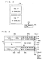
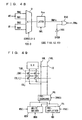
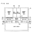
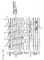
- Fig. 58 is a diagram representing an example of an arrangement of a conventional DRAM built-in system LSI.
- the DRAM built-in system LSI has a logic circuit LG and a DRAM macro integrated on the same semiconductor substrate chip CH.
- the DRAM macro includes memory arrays MA0 and MA1, each having a plurality of memory cells arranged in a matrix of rows and columns; row decoders XD0 and XD1 provided corresponding to memory arrays MA0 and MA1 for selecting addressed rows of the corresponding memory arrays MA0 and MA1; column decoders YD0 and YD1 provided corresponding to memory arrays MA0 and MA1 for selecting addressed columns of memory arrays MA0 and MA1; data paths DP0 and DP1 for communicating data with the memory cell columns selected by column decoders YD0 and YD1; and a control circuit CG for controlling the data access operation to memory arrays MA0 and MA1.
- Data paths DP0 and DP1 are coupled to logic circuit LG via data buses DB0 and DB1, and control circuit CG is coupled to logic circuit LG via a control bus CTB.
- each of data buses DB0 and DB1 separately communicates 128-bit write data (D) and 128-bit read data (Q).
- row decoders XD0 and XD1 are disposed orthogonal to column decoders YD0 and YD1.
- data paths DP0 and DP1 can be coupled to the selected columns of memory arrays MA0 and MA1 in the shortest distance.
- data buses DB0 and DB1 are not in any way limited with respect to the pitch condition and number of pin terminals so that a wide bus can be implemented.
- Fig. 59 is a schematic representation of an arrangement of memory arrays MA0 and MA1 shown in Fig. 58. Since these memory arrays MA0 and MA1 have identical arrangement, they are generically shown as memory array MA in Fig. 59.
- Memory array MA includes a plurality of memory cell blocks MCB arranged in a matrix of rows and columns. Though not specifically shown, memory cells are arranged in a matrix of rows and columns within these memory cell blocks MCB.
- Local IO line pair groups LIOs are provided corresponding to each of memory cell blocks MCB for communicating data with the corresponding memory cell blocks.
- a local IO line pair LIO communicates signals complementary one another.
- a sense amplifier group SAs is arranged corresponding to each of memory cell blocks MCB.
- Sense amplifier group SAs has a shared sense amplifier arrangement and is shared by the memory cell blocks adjacent to one another in the column direction.
- These sense amplifier groups SAs includes sense amplifier circuits SA provided corresponding to the respective columns of the corresponding memory cell blocks, and perform sense, amplification, and latching of data of the columns of the corresponding memory cell blocks during activation.
- Sense amplifier group SAs is selectively coupled to the corresponding local IO line pair group LIOs.
- Word line group WLs is disposed in common to memory cell blocks MCB arranged in alignment in the row direction. In operation, one word line WL of word line group WLs contained in one row block (or the block consisting of the memory cell blocks arranged in alignment in the row direction) is driven to the selected state.
- Global IO line pairs GIO0 to GIO127 that extend in the column direction are disposed in regions between the memory cell blocks adjacent to one another in the row direction and a region outside of the memory cell blocks (these regions hereinafter referred to as inter-block regions).
- Four global IO line pairs are arranged in common to the memory cell blocks aligned in the column direction.
- Four local IO line pairs LIO are provided to each memory cell block, and a group of the four local IO line pairs LIOs correspondingly provided to each memory cell block MCB in one row block are coupled to the corresponding global IO line pairs via IO switches IOSW, respectively.
- Each of global IO line pairs GIO0 to GIO127 transmits complementary signals, is coupled to a data path shown in Fig. 58, and is coupled to logic circuit LG via a write/read circuit within the data path.
- Column select lines CSL are arranged extending in the column direction over memory cell array MA in the same interconnection layer as global IO line pairs GIO0 to GIO127.
- Column select line group CSLs are shared by memory cell blocks MCB disposed in alignment in the column direction.
- IO switches IOSW local IO line pair groups LIOs of a selected row block are coupled to global IO line pairs GIO0 to GIO127, while local IO line pair groups LIOs of non-selected row blocks are disconnected from global IO line pairs GIO0 to GIO127.
- four columns are simultaneously selected in each column block (or the block consisting of the memory cell blocks arranged in alignment in the column direction), and four local IO line pairs LIO are respectively coupled to the corresponding global IO line pairs.
- global IO line pairs GIO0 to GIO127 are coupled to logic circuit LG via the data paths. Therefore, increasing the bus width of data buses DB0 and DB1 between the DRAM macro and the logic circuit means increasing the number of global IO line pairs.
- a global IO line pair is a complementary signal line pair, and the increase in number of inter-block regions results in the increase in the area occupied by the global IO line pairs in a memory cell array and in the increase in the area of the region occupied by transfer gates connecting global IO line pairs GIO and local IO line pair LIO, which leads to a greater chip area.
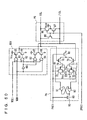
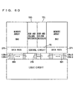
- Fig. 60 is a schematic representation of another conventional DRAM built-in system LSI.
- the arrangement shown in Fig. 60 is presented, for instance, by Yabe et al. in Digest of Technical Papers, 1999 IEEE ISSCC, on pp. 72 to 73 and p. 415.
- row decoders XD0 and XD1 as well as column decoders YX0 and YX1 are disposed in the region between memory arrays MA0 and MA1.
- row decoders and column decoders are provided within the same region.
- the column decoders are not disposed between memory arrays MA0 and MA1 and data paths DP0 and DP1.
- Control circuit CG is disposed in the region between data paths DP0 and DP1.
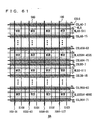
- Fig. 61 is a schematic representation of an arrangement of memory arrays MA0 and MA1 shown in Fig. 60.
- memory array MA (MA0, MA1) includes memory cell blocks MCB arranged in alignment both in the row direction and in the column direction.
- a sense amplifier band SAB including sense amplifier circuits is arranged corresponding to these memory cell blocks MCB.
- a column select line group CSLG extending in the row direction is arranged in the region of sense amplifier band SAB.
- a column select line group CSLG includes 8-bit column select lines CSLAi to CSLA(i+7) or CSLBi to CSLB(i+7).
- a word line group WLG is provided in parallel to these column select line groups CSLG.
- Word line group WLG includes 512 word lines WLAj to WLA(j+511) or WLBj to WLB(j+511).
- N is 0 or a natural number.
- 32-bit IO line group IOG extending in the column direction is provided over memory cell blocks MCB aligned in the column direction.
- one spare IO data line pair SIO is provided in parallel to IO data line pair group IOG. Since a row block includes four memory cell blocks MCB, four spare IO data line pairs SIO0 to SIO3 are provided.
- the column select lines are divided into two groups of column select lines CSLA0 to CSLA71 and CSLB0 to CSLB71, because two word lines may be simultaneously driven to the selected state in this memory array, and the data of a memory cell connected to one of these two word lines is to be read. Therefore, the sense amplifier band through which column select lines CSLA64 to CSLA71 pass and the sense amplifier band through which column select lines CSLB0 to CSLB7 pass are separately provided so as to allow one word line from word lines WLA3584 to WLA4095 and one word line from word lines WLB0 to WLB511 to be simultaneously driven to the selected state.
- 16 sense amplifiers per memory cell block MCB are coupled via column select gates to the respective IO data line pairs IO0 to IO127.
- One column select gate (per IO) is rendered conductive by a column select line. Since the column select gate is coupled to an IO data line pair, an IO switch for connecting a local IO line pair and a global IO line pair is not required.
- column select lines are disposed orthogonal to IO data line pairs, and the IO data line pairs are arranged extending over the memory cell array, so that there is no need to provide an interconnection region specially for the IO data line pairs, and the chip area can be reduced.
- Fig. 62 is a schematic diagram representing an arrangement of a sense amplifier band for one memory cell block MCB.
- Fig. 62 shows a memory cell block to which column select lines CSLA0 to CSLA15 are provided.
- eight sense amplifier circuits SA are disposed in one sense amplifier band. Each sense amplifier circuit SA is connected to a corresponding IO data line pair via a column select gate YG. While IO data line pairs IO0 and IO1 are shown in Fig. 62, 32-bit IO data line pairs IO0 to IO31 are provided to memory cell block MCB.
- one spare IO data line pair SIO is provided for the 32-bit IO data line pairs.
- Eight spare sense amplifier circuits are also disposed in one sense amplifier band for the spare IO data line pair SIO.
- one sense amplifier circuit is selected from a set of eight sense amplifier circuits as a unit, and the selected sense amplifier circuit is coupled to a corresponding IO data line pair via column select gate YG.
- Two sense amplifier bands are provided to a memory cell block. Since one of 16 column select lines CSLA0 to CSLA15 is driven to the selected state, 16 sense amplifier circuits are correspondingly provided to one IO data line pair. The same is true for the spare sense amplifier circuits.
- 32 columns out of 512 columns are simultaneously selected and connected to the corresponding IO data line pairs in memory cell block MCB by the column select lines. Defective bits repair for an IO data line pair is effected by replacing a set of 16 sense amplifier circuits with a set of 16 spare sense amplifier circuits.
- Column select lines CSLA0 to CSLA15 each select the normal sense amplifier circuit and the spare sense amplifier circuit at the same time as shown in Fig. 62, and the data from the normal sense amplifier circuit and the data held by the spare sense amplifier circuit are simultaneously transferred to IO data line pairs and the spare IO data line pair.
- a sense amplifier circuit is coupled to an IO data line pair via column select gate YG, the region for disposing transfer gates is no longer necessary.
- IO data line pairs IO are disposed extending over the memory cell array in the column direction, an increase in the number of IO data line pairs does not in any way require an increase in the area occupied by IO data line pairs.
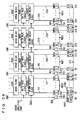
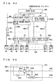
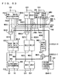
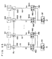
- Fig. 63 is a schematic diagram representing an arrangement of a data path of the DRAM macro shown in Fig. 60.
- Fig. 63 shows an arrangement of a 32-bit data path, i. e. an arrangement corresponding to one column block.
- the data path includes preamplifiers PA0 to PA31, write drivers WDV0 to WDV31, and a spare preamplifier SPA and a spare write driver SWDV provided corresponding to spare IO data line pair SIO.
- Preamplifiers PA0 to PA31 and spare preamplifier SPA amplify and output the data on IO data line pairs IO0 to IO31 and spare IO data line pair SIO.
- Write drivers WDV0 to WDV31 and spare write driver SWDV are activated according to a write driver enable signal WDE to drive the corresponding IO data line pairs IO0 to IO31 and spare IO data line pair SIO according to the received write data.
- Write data mask signals /DM0 to /DM3 inhibiting a data write are also provided to write drivers WDV0 to WDV31. Each of these write data mask signals /DM0 to /DM3 inhibits writing of 8 bits of data as a unit.
- data mask signals /DM0 to /DM3 and /DMS are activated instructing that the data write is to be masked, the corresponding write drivers attain the output high impedance state.
- Preamplifiers PA0 to PA31, spare preamplifier SPA, write drivers WDV0 to WDV31, and a spare write driver SWDV each include a circuit for equalizing the corresponding data line pair according to an IO equalizing instruction signal IOEQ.
- the data path further includes a column redundancy control circuit CRC for determining, according to row block address signals RBA0 to RBA3 designating a row block in the selected state, whether a defective column is addressed in a normal memory cell array, and according to the determination result, outputting selecting signals SIOSEL0 to SIOSEL31 designating an IO data line pair to be replaced by spare IO data line pair, and for generating signals SDMSEL0 to SDMSEL3 signaling whether to mask the spare memory cell data according to a data mask signal during a data write; 2:1 multiplexers MUX0 to MUX31 for selecting, according to selecting signals SIOSEL0 to SIOSEL31, one of the signals output from the corresponding preamplifiers PA0 to PA31 and spare preamplifier SPA; read data latches RDL0 to RDL31 provided corresponding to the respective 2:1 multiplexers MUX0 to MUX31 for taking in and outputting output signals RDF0 to RDF31 of multiplexers MUX0 to MUX31 in synchronization
- Read data latches RDL0 to RDL31 take in the received data at the fall of clock signal CLK and attain the latching state at the rise of clock signal CLK.
- Output buffers QB0 to QB31 take in and output the output data of read data latches RDL0 to RDL31 in response to the rise of clock signal CLK.
- the data path further includes input buffers DB0 to DB31 provided corresponding to the respective write data D0 to D31 from outside for taking in the received write data in synchronization with clock signal CLK; 32:1 spare multiplexer SMUX for selecting, according to spare IO selecting signal SIOSEL0 to SIOSEL31 from column redundancy control circuit CRC, one of internal write data WD0 to WD 31 output from input buffers DB0 to DB31; write data latches WDL0 to WDL31 for taking in internal write data WD0 to WD 31 from input buffers DB0 to DB31 in response to write driver enable signal WDE; a spare write data latch SWDL for taking in and outputting internal write data WDS from spare multiplexer SMUX in response to write driver enable signal WDE; write drivers WDV0 to WDV31 for driving IO data line pairs IO0 to IO31 according to output data WDD0 to WDD31 from write data latches WDL0 to WDL31 when activated in response to the activation of write driver enable
- a DRAM macro has a multi-bank arrangement.
- write command WRITE instructing a data write is taken in along with a column bank address CBK indicating the bank to which a column access is made.
- a column address signal indicating the selected column (not shown) is also taken in.
- An internal circuit not shown, stores row block address signals RBA0 to RBA3 indicating a row block in the active state, and applies the stored row block address signals RBA0 to RBA3 to column redundancy control circuit CRC when write command WRITE is provided.
- An address indicating the IO data line pair to which a defective memory cell is connected for each row block is programmed in column redundancy control circuit CRC.
- An address signal indicating a defective IO data line pair of the row block is decoded according to row block address signals RBA0 to RBA3 to generate spare IO selecting signals SIOSEL0 to SIOSEL31.
- input buffers DB0 to DB31 are activated, take in write data D0 to D31 from outside, and generate internal write data WD0 to WD31 that are latched into write data latches WDL0 to WDL31.
- Spare multiplexer SMUX selects one of the output data from input buffers DB0 to DB31 according to spare IO selecting signals SIOSEL0 to SIOSEL31 from column redundancy control circuit CRC and applies the selected output data to spare write data latch SWDL.
- write driver enable signal WDE is driven to the active state or the logic high or "H” level, and IO equalizing instruction signal IOEQ attains the inactive state or the logic low or “L” level.
- IO equalizing instruction signal IOEQ attains the inactive state or the logic low or “L” level.
- the precharging/equalizing operation of IO data line pairs IO0 to IO31 and spare IO data line pair SIO is completed, and write data is transmitted to these data line pairs IO0 to IO31 and SIO.
- a column decoder (not shown) performs a column select operation, and a column select line CSL corresponding to the addressed column is driven to the selected state or the "H" level. Consequently, data are written into memory cells via IO data line pairs IO0 to IO31 and spare IO data line pair SIO.
- column select line CSL is deactivated, and thereafter, the deactivation of write driver enable signal WDE as well as the activation of IO equalizing instruction signal IOEQ causes IO data line pairs IO0 to IO31 and spare IO data line pair SIO to be equalized and precharged to the power supply voltage level again.
- a column bank address CBK and a column address signal (not shown) are taken in at the rising edge of clock signal CLK, as in the data write operation.
- Row block address signals RBA0 to RBA3 are applied to column redundancy control circuit CRC as in the data write operation according to read command READ and column bank address CBK, and column redundancy control circuit CRC drives one of spare IO line selecting signals SIOSEL0 to SIOSEL31 to the selected state.
- equalizing signal IOEQ is deactivated, and the equalizing operation for IO data line pairs IO0 to IO31 and spare IO data line pair SIO is completed.
- the column decoder drives column select line CSL to the selected state, memory cell data is read out to these IO data line pairs IO0 to IO31 and spare IO data line pair SIO.
- a preamplifier activating signal PAE is activated and preamplifiers PA0 to PA31 and spare preamplifier SPA amplify and latch the signals on these IO data line pairs IO0 to IO31 and spare IO data line pair SIO.
- Preamplifiers PA0 to PA31 and spare preamplifier SPA each include flip-flop, and maintain and output valid data even after the deactivation of preamplifier activating signal PAE.
- preamplifier activating signal PAE is deactivated, and column select signal line CSL is also driven to the inactive state.
- equalizing signal IOEQ is activated, and IO data line pairs are precharged and equalized to a prescribed power supply voltage level again.
- 2:1 multiplexers MUX0 to MUX31 perform the selecting operation according to spare IO selecting signals SIOSEL0 to SIOSEL31 from column redundancy control circuit CRC, and one of the output signals PAO0 to PAO31 of preamplifiers PA0 to PA31 is replaced by an output signal PAOS from spare preamplifier SPA when a defective memory cell is addressed.
- read data latches RDL0 to RDL31 latch output signals RDF0 to RDF31 of multiplexers MUX0 to MUX31 in response to the rise of clock signal CLK.
- Output buffers QB0 to QB31 take in data RD0 to RD31 from read data latches RDL0 to RDL31 in synchronization with the clock signal and output the output data Q0 to Q31 to logic circuit LG.
- column select lines CSL (CSLA0 to CSLA71 and CSLB0 to CSLB71) are disposed in parallel to the word lines in a sense amplifier band accompanies a column redundant arrangement for one IO data line pair, i. e. it has an arrangement of replacing the IO data line pair with a spare IO data line pair.
- the IO data line pairs are driven by write driver WDV0 to WDV31 and spare write driver SWDV.
- column select line CSL is first driven to the selected state and the IO data line pairs are driven by sense amplifier circuits.
- the replacement of IO data line pairs is carried out.
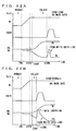
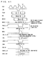
- the timing at which the result of spare determination is made definite is the same for a data write mode and for read mode, and in the data write mode, column select line CSL is driven to the selected state at a timing later than that in the read operation mode during which data read is performed. Therefore, when the read operation is performed in the cycle following the write operation, as shown in Fig. 64, the equalizing time ⁇ Teq(wr) for an IO data line pair becomes shorter than the equalizing time ⁇ Teq(rr) when a data read is performed in the cycle following the read operation.
- the cycle time When the cycle time is made shorter, the data read would be performed before IO data line pairs IO0 to IO31 and spare IO data line pair SIO are sufficiently precharged and equalized, so that amplification by a preamplifier cannot be accurately performed, resulting in the so-called "write recovery" problem.
- the cycle time could not be shortened to implement a high-speed operation.
- the equalizing time ⁇ Teq(wr) may be ensured by delaying the timing at which column select line CSL is activated in the data read operation mode.
- the activation of preamplifier activating signal PAE is delayed accordingly, and thus, the timing of output data RDF0 to RDF31 of multiplexers MUX0 to MUX31 becoming definite is also delayed. Consequently, read data latches RDL0 to RDL31, in response to the rise of clock signal CLK, have entered the latched state so that there is no margin for the set-up time ⁇ Ts of input signals RDF0 to RDF31 to read data latches RDL0 to RDL31 relative to clock signal CLK, and an accurate reading of data cannot be ensured.
- data bit widths differ according to the uses. From the viewpoint of the production cost, it is preferable to form common parts for DRAM macros of various data bit widths, and to change the arrangement of the input/output circuits according to the data bit widths. Therefore, in this case, the same numbers of write drivers and input buffers are provided regardless of the data bit width. The number of input buffers actually used are changed according to the data bit width, and write drivers are selectively coupled to the input buffers being used.
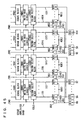
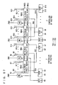
- Fig. 65 is a schematic representation of an arrangement of a data write portion of a DRAM macro shown in Fig. 63 where the data bit width is reduced to one-fourth of its original width.
- input buffers DB0 to DB7 are provided for write data bits D0 to D7, respectively.
- Write drivers WDV0 to WDV31 of 32 bits are provided corresponding to input buffers, where four write drivers as a unit correspond to one input buffer.
- input buffer DB0 is coupled to write drivers WDV0 to WDV3
- input buffer DB7 is coupled to write drivers WDV28 to WDV31.
- These write drivers WDV0 to WDV31 are coupled to IO data line pairs IO0 to IO31, respectively.
- Write drivers WDV0, WDV4, ... WDV28 are activated in response to a write driver enable signal WDE0.
- Write drivers WDV3, WDV7, ... WDV31 are activated in response to a write driver enable signal WDE3.
- a write data mask instruction signal /DM0 is applied to write drivers WDV0 to WDV7.
- a write data mask instruction signal /DM3 is applied to write drivers WDV24 to WDV31.
- each of write data mask instruction signals /DM0 to /DM3 masks the write data on corresponding eight IO data line pairs as a unit.
- a data write operation is considered under this condition.
- write driver enable signal WDE0 is rendered active and write drivers WDV0, WDV (4k), ... WDV28 are rendered active.
- write data mask instruction signals /DM0 to /DM3 are all rendered inactive, and a data write operation is performed.
- IO data line pairs IO0 to IO31 are coupled to sense amplifier circuits (S.A) SA0 to SA31 via selected column select gates CSG0 to CSG31, respectively.
- S.A sense amplifier circuits
- Non-selected write drivers are in the output high impedance state.
- write drivers WDV0, ..., WDV (4k), ... WDV28 transfer data corresponding to write data bits D0 to D7 to sense amplifiers SA0, SA (4k), ... SA28.
- IO data line pairs excluding the IO data line pairs IO0, ..., IO (4k), ... IO28 are precharged to a power-supply voltage Vcc level (see Fig. 64).
- a corresponding column select gate CSG is in the conductive state according to a column select signal CSL, and a non-selected sense amplifier circuit (S.A) receives this precharge voltage Vcc so that the latch data of the non-selected sense amplifier circuit (S.A) may possibly become inverted.
- a write driver is set to the inactive state according to a data write mask instruction signal
- an internal data write circuit that accommodates different data bit widths cannot be implemented.
- common chips cannot be used to adapt to the different data bit widths so that each chip will need to be designed individually according to the data bit width, which leads to a problem of higher production cost.
- a memory device with column redundancy is disclosed in EP 0 559 368 A2.
- the memory has a plurality of columns of memory cells and a plurality of redundant columns of memory cells.
- a redundant write generator and write fuses are provided for each write portion to replace the defective column with a redundant column by replacing a write global data line with a redundant write global data line.
- Redundant read generators and read fuses are provided for each read portion to replace a defective column by deselecting a read global data line and replacing it with a redundant read global data line.
- An object of the present invention is to provide a logic-merging DRAM operable in synchronization with a high-speed clock signal.
- Another object of the present invention is to provide a logic-merging DRAM capable of performing a data write at a high speed.
- the timing for a column select can be optimized for both a data write and a data read, thereby achieving a high-speed access.
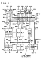
- Fig. 1 is a schematic representation of an overall arrangement of a DRAM built-in system LSI according to the present invention.
- the DRAM built-in system LSI includes a logic circuit LG, and a DRAM macro for storing data for logic circuit LG.
- the DRAM macro includes two memory cell arrays MA0 and MA1, each divided into 32 row blocks R#0 to R#31. Row blocks R#0 to R#15 of memory cell arrays MA0 and MA1 form a bank BA#0, and row blocks R#16 to R#31 of memory cell arrays MA0 and MA1 form a bank BA#1.
- a read data line pair IOR for transmitting data from a selected memory cell and a write data line pair IOW for transmitting write data to a selected memory cell are disposed extending in the column direction over memory cell arrays MA0 and MA1.
- Read data line pair IOR and write data line pair IOW are coupled to data paths DP0 and DP1 provided to memory cell arrays MA0 and MA1, respectively.
- Data paths DP0 and DP1 are coupled to logic circuit LG via data buses DB0 and DB1, respectively.
- Data buses DB0 and DB1 also transmit write data and read data via separate buses.
- a decoder disposing region XYD0 for disposing a decoder for memory cell array MA0 as well as a decoder disposing region XYD1 for memory cell array MA1 is provided between memory cell arrays MA0 and MA1.
- Decoder disposing regions XYD0 and XYD1 include a row decoder provided corresponding to each of the row blocks, for selecting a memory cell row in the corresponding row block, a read column decoder provided corresponding to each row block for selecting a column to perform a data read of the corresponding row block, and a write column decoder provided corresponding to each row block for selecting a memory cell column to perform a data write of the corresponding row block.
- a control circuit CG for controlling the memory cell selecting operation is provided in the region between data paths DP0 and DP1.
- logic circuit LG includes a product-sum operation circuit that performs product-sum operation of data transmitted through data buses DB0 and DB1.
- Fig. 2 is a schematic representation of an arrangement of one bank BA in one memory cell array in the DRAM macro shown in Fig. 1.
- bank BA includes pages “0" and “1,” each consisting of eight row blocks.
- word lines are simultaneously driven to the selected state.
- a page address is provided to a page address latch PGL, and according to a page selecting signal PGS from page address latch PGL, one of pages "0" and "1" is selected.
- Driving two word lines simultaneously to the selected state reduces the overhead in a page switching in a bank.
- Fig. 3 is a schematic representation of an arrangement of a portion related to one row block.
- a word line WL is disposed extending in the row direction in this row block R#.
- Sense amplifier bands SB#a and SB#b are arranged on two sides of row block R#. Within a page, sense amplifier bands SB#a and SB#b each are shared by the row blocks adjacent to one another in the column direction. As for the row block at a page boundary, sense amplifier bands are separately provided for the respective row blocks in the boundary region.
- a read column select line group RCSLs and a write column select line group WCSLs are arranged in parallel with word line WL in sense amplifier bands SB#a and SB#b.
- a read column decoder RYDa is provided for sense amplifier band SB#a and a read column decoder RYDb is provided for sense amplifier band SB#b in order to select a read column select line from read column select line group RCSLs.
- Write column decoders WYDa and WYDb are provided corresponding to sense amplifier bands SB#a and SB#b in order to select a write column select line from write column select line group WCSLs.
- Read column decoders RYDa and RYDb receive a read column address signal YR, page selecting signal PGS, and row block activating instruction signals RBact1 and RBact2 to perform a decoding operation.
- Write column decoders WYDa and WYDb perform a decoding operation according to a write column address signal YW, page selecting signal PGS, and row block activating instruction signals RBact1 and RBact2.
- Row block activating instruction signals RBact1 and RBact2 instructs that one of row block R# and the row block adjacent to and above (or below) row block R# is in the active state, and that one word line WL in either of the row blocks is maintained at the selected state so that sense amplifier band SB#a (or SB#b) is in the active state.
- a row decoder XD that receives a row block designating signal RBS and an X address signal XA is provided for selecting word line WL.
- Row block designating signal RBS is generated from a row block address signal and a bank address signal.
- Row decoder XD has internally a latch circuit, and maintains the selected state of word line WL until a precharge instruction signal is provided, even after row block designating signal RBS is driven to the non-selected state.
- the decoders shown in Fig. 3 are arranged corresponding to each row block in decoder disposing regions XYD0 and XYD1 shown in Fig. 1.
- Row block activating instruction signal RBact1 is activated by a row block designating signal RBS indicating row block R# shown in Fig. 3 and by row block designating signal RBS for the row block adjacent to and above row block R#.
- Row block activating instruction signal RBact2 is generated based on row block designating signals for row block R# and the row block adjacent to and below row block R#.
- Row block designating signal RBS is driven to the active state in a row access (or upon application of an active command).
- column decoders are respectively provided for sense amplifier bands SB#a and SB#b, and the column decoder is activated depending on whether or not the row block sharing the corresponding sense amplifier band is in the active state.
- the column decoder is arranged such that the column decoder is activated according to a column bank address provided in a column access, so that a column select operation is performed.
- pages of one bank BA are shown being divided into an upper half block and a lower half block. Pages "0" and “1" may, however, be arranged alternately by row-by-row block basis.
- two word lines per page is driven to the selected state.
- a page address signal an address signal that corresponds to a page designating signal PGS
- PGS page designating signal
- the active state of a corresponding sense amplifier band is detected.
- the column decoder is activated, and the column select line is driven to the selected state according to the column select signal.
- the column select operation can be activated for the column decoder provided for each sense amplifier band depending on whether the corresponding sense amplifier band is in the active state.
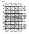
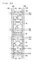
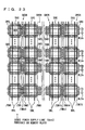
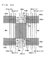
- Fig. 4 is a schematic representation of an arrangement of one memory array MA. Sixteen row blocks R#0 to R#15 contained in one bank are shown in Fig. 4. Sense amplifier bands SB# are disposed on either side of row blocks R#0 to R#15 in the column direction. At the page boundary, sense amplifier bands SB#8 and SB#9 are provided for row blocks R#7 and R#8, respectively. 8-bit read column select lines CSLR and an 8-bit write column select lines CSLW are arranged in each of sense amplifier bands SB#0 to SB#17. A page is provided with 72 read column select lines CSLRA0 to CSLRA71 (or CSLRB0 to CSLRB71) and 72 write column select lines CSLWA0 to CSLWA71 (CSLWB0 to CSLWB71).
- 512 word lines WLA (or WLB) are disposed for each of row blocks R#0 to R#15.
- Read data line pairs IOR0 to IOR127 and write data line pairs IOW0 to IOW127 are arranged extending in the column direction over the memory cell array.
- 32-bit data line pairs one spare read data line pair SIOR and one spare write data line pair SIOW are provided.
- 32-bit data line pairs IOR and IOW are provided for memory cell blocks MCB aligned in the column direction (column blocks). The data line pairs are replaced in a unit of a column block.
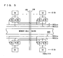
- Fig. 5 is a schematic representation of an arrangement of a portion related to one data line pair.
- Eight sense amplifier circuits SA are provided above memory cell block MCB and eight other sense amplifier circuits SA are provided below memory cell block MCB for a read data line pair IOR and a write data line pair IOW.
- a read gate RG for coupling a corresponding sense amplifier circuit SA to read data line pair IOR
- a write gate WG for coupling a corresponding sense amplifier circuit SA to write data line pair IOW are provided.
- An 8-bit read column select line group RCSLas and an 8-bit write column select line group WCSLas are arranged above memory block MCB, and an 8-bit read column select line group RCSLbs and an 8-bit writhe column select line group WCSLbs are arranged below memory block MCB.
- One of the 16-bit read column select line groups RCSLas and RCSLbs is driven to the selected state (upon access to memory cell block MCB), or one of the 16-bit write column select line groups WCSLas and WCSLbs is driven to the selected state.
- 16 sense amplifier circuits SA are disposed for one read data line pair IOR and one write data line pair IOW.
- a spare read data line pair and a spare write data line pair are provided with 16 spare sense amplifier circuits.
- the replacement is performed in a unit of 16 sense amplifier circuits (replacement of a data line pair).
- Fig. 6 is a schematic representation of an arrangement of a sense amplifier band related to one sense amplifier circuit.
- sense amplifier SA is coupled to bit lines BLU and BLU of the upper memory cell block via a bit line isolating gate BGU, and is also coupled to bit lines BLL and BLL of the lower memory cell block via a bit line isolating gate BGL.
- Bit line isolating gates BGU and BGL are rendered conductive according to bit line isolating instruction signals BLIU and BLIL in their standby state, and only the memory cell block containing a selected memory cell is coupled to sense amplifier circuit SA in the active cycle.
- Sense amplifier circuit SA includes cross-coupled P-channel MOS transistors PQ1 and PQ2, a P-channel MOS transistor PQ3 for transmitting a sense power supply voltage VccS to the sources of MOS transistors PQ1 and PQ2 in response to activation of a sense amplifier activating signal /SOP, cross-coupled N-channel MOS transistors NQ1 and NQ2, and an N-channel MOS transistor NQ3 rendered conductive in response to activation of a sense amplifier activating signal SON for transmitting the ground voltage to the sources of these MOS transistors NQ1 and NQ2.
- sense amplifier circuit SA senses, amplifies, and latches the memory cell data on sense nodes SNa and SNb.
- Write gate WG includes transfer gates TGa and TGb rendered conductive in response to a column select signal on write column select line CSLW and electrically couple sense nodes SNa and SNb to write data lines IOWL and /IOWL.
- Read gate RG includes N-channel MOS transistors TGe and TGf having their respective gates connected to sense nodes SNa and SNb, and N-channel MOS transistors TGc and TGd rendered conductive according to a signal on read column select line CSLR and electrically couple the drain nodes of these MOS transistors TGe and TGf to read data lines /IORL and IORL.
- Read gate RG has one of MOS transistors TGe and TGf rendered conductive in response to a signal potential on sense nodes SNa and SNb, and discharges one of read data lines IORL and /IORL toward the ground voltage level.
- Precharging/equalizing circuit P/E includes an N-channel MOS transistor TGg rendered conductive during activation of bit line equalizing instruction signal BLEQ to short-circuit sense nodes SNa and SNb, and N-channel MOS transistors TGh and TGi rendered conductive during activation of bit line equalizing instruction signal BLEQ to transmit intermediate voltage VBL to each of the sense nodes SNa and SNb.
- column select line CSLR can be driven to the selected state prior to completion of the sensing operation of sense amplifier circuit SA, so that a high-speed data read is achieved (since data read operation of read gate RG does not affect the sensing operation of sense amplifier circuit SA).
- Fig. 7 is a schematic representation of an arrangement of a data path that inputs and outputs data of 32 bits.
- preamplifiers PA0 to PA31 are provided corresponding to the respective read data line pairs IOR0 to IOR31, and write drivers WDV0 to WDV31 are provided corresponding to the respective write data line pairs IOW0 to IOW31.
- a spare preamplifier SPA is provided to a spare read data line pair SIOR, and a spare write driver SWDV is provided to a spare write data line pair SIOW.
- Column redundancy control circuit CRC generates a spare data line selecting signal SIOSEL at different timings for a data write and for a data read, and provides spare data line selecting signal SIOSEL to multiplexers MUX0 to MUX31 and SMUX.
- a read data line pair equalizing instruction signal IOREQ is provided to preamplifiers PA0 to PA31 and spare preamplifier SPA, and a write data line pair equalizing instruction signal IOWEQ is provided to write drivers WDV0 to WDV31 and spare write driver SWDV.
- preamplifiers PA0 to PA31, spare preamplifier SPA, write drivers WDV0 to WDV31, and spare write driver SWDV can also function to precharge and equalize the corresponding data line pairs.
- the read data line pairs are equalized for the following reasons.
- Read data line pairs IOR0 to IOR31 and spare read data line pair SIOR are complementary signal line pairs and are small in potential change during a data read.
- Preamplifiers PA0 to PA31 and spare preamplifier SPA amplify the very small potential difference of the corresponding read data line pair IOR. Therefore, a read data line pair must be brought to an equal potential before a column select line is activated so that accurate potential change that corresponds to the memory cell data may be generated on the read data line pair. In other words, when a preamplifier is activated at a prescribed timing after the column select line is activated, a potential difference already large enough for the amplification operation of the preamplifier needs to be generated on the read data line pair.
- equalizing instruction signal IOWEQ is provided to write drivers WDV0 to WDV31 and spare write driver SWDV for the following reasons.
- Write data line pairs IOW0 to IOW31 and spare write data line pair SIOW are also complementary signal line pairs.
- write mask data /DM0 to /DM3 and /DMS are utilized to mask the data write. If the write data line pair subject to masking the data write was not maintained at an equal potential, even if the write driver is set to the output high impedance state according to write mask data, a potential difference is generated on the complementary write data lines, and the write column select line is activated to couple the corresponding sense amplifier circuit to the write data line pair having the potential difference.
- the electrical charge flowing from the write data line pair having a large parasitic capacitance may possibly cause the inversion of the data held in the sense amplifier circuit.
- the write data line pair is set at an equal potential prior to a data write operation.
- Column redundancy control circuit CRC outputs spare data line selecting signal SIOSEL at different timings for a data write and for a data read so as to difference the timing for outputting the result of spare determination for a data read and for a data write.
- the result of spare determination is output earlier to advance the activation of the write column select line.
- the timing at which the result of spare determination is output is delayed so that, after read column select line RCSL is activated at an early timing, and when the output data from the preamplifier becomes definite, the memory cell data is selected according to the result of the spare determination.
- Multiplexers MUX0 to MUX31 are provided to preamplifiers PA0 to PA31, respectively, and perform the selecting operation according to spare data line selecting signals SIOSEL0 to SIOSEL31 in a read operation.
- Read data latches RDL0 to RDL31 for taking in and outputting a signal provided in synchronization with clock signal CLK are provided corresponding to multiplexers MUX0 to MUX31.
- Output buffers QB0 to QB31 for performing data output operation in synchronization with clock signal CLK are provided for read data latches RDL0 to RDL31, respectively.
- Input buffers DB0 to DB31 are provided for a write data, and write data latches WDL0 to WDL31 are provided to these input buffers DB0 to DB31, respectively.
- multiplexer SMUX for performing the selecting operation according to spare data line selecting signal SIOSEL from column redundancy control circuit CRC is provided for input buffers DB0 to DB31.
- Spare write data latch SWDL is provided for multiplexer SMUX.
- Write command WRITE instructing a data write is provided at time T0 or at time T1.
- column bank address CBK and a page address for designating a column access bank (to which a column select operation is performed) as well as a column address are provided.
- row block address signals RBA0 to RBA3 for specifying a row block to be accessed are generated from a circuit (not shown but described later) and are provided to column redundancy control circuit CRC.
- column redundancy control circuit CRC When write command WRITE is provided, column redundancy control circuit CRC performs a spare determination operation at a relatively early timing, and drives, among spare data line selecting signals SIOSEL 0-3, the spare data line selecting signal indicating a defective write data line pair to the active state.
- Input buffers DB0 to DB31 take in the externally provided write data D0 to D31 in synchronization with clock signal CLK and generate internal write data WD0 to WD31.
- One of internal write data WD0 to WD31 from input buffers DB0 to DB31 is selected by multiplexer SMUX according to spare data line selecting signals SIOSEL0 to SIOSEL31 from column redundancy control circuit CRC, and is provided to spare write data latch SWDL.
- Write column select line CSLW is driven to the active state according to a column address signal substantially at the same time as the activation of write driver enable signal WDE.
- write driver WDV0 to WDV31 and spare write driver SWDV drive write data line pairs IOW0 to IOW31 and spare write data line pair SIOW according to the provided data.
- write column select line CSLW and write driver enable signal WDE are deactivated.
- equalizing instruction signal IOWEQ is activated, and write data line pairs IOW0 to IOW31 and spare write data line pair SIOW are precharged and equalized to a prescribed voltage level.
- read command READ instructing a data read is provided at time T2 and time T3.
- row block address signals RBA0 to RBA3 designating a row block to be accessed is generated according to column bank address CBK designating the column bank subject to a column access and a page address (not shown).
- Column redundancy control circuit CRC performs the spare determination operation according to address signals RBA0 to RBA3 for specifying the row block.
- read column select line CSLR in the row block to be column-accessed is activated according to a column address signal and column bank address CBK and a page address signal, and data in the memory cells on the selected columns (i. e. data latched from the sense amplifier circuit) are read on respective read data line pairs IOR0 to IOR31 and spare read data line pair SIOR.
- the equalizing of the read data line pair is stopped immediately before the activation of read column select line CSLR (i. e. deactivation of equalizing instruction signal IOREQ).
- the potentials of read data line pairs IOR0 to IOR31 and spare read data line pair SIOR change according to the read data.
- preamplifier activating signal PAE is activated, and preamplifiers PA0 to PA31 and spare preamplifier SPA operate to amplify the signal potential on the corresponding read data line pair, and internal read data PAO0 to PAO31 and PAOS become definite.
- multiplexers MUX0 to MUX31 When read data PAO0 to PAO31 and PAOS from preamplifiers PA0 to PA31 and spare preamplifier SPA are made definite, multiplexers MUX0 to MUX31 perform the selecting operation according to spare data line selecting signals SIOSEL0 to SIOSEL31 from column redundancy control circuit CRC. Data RDF0 to RDF31 from multiplexers MUX0 to MUX31 are latched at the rise of clock signal CLK by read data latches RDL0 to RDL31, and thereafter, are output as output data Q0 to Q31 via output buffers QB0 to QB31 in synchronization with the rise of clock signal CLK.
- the read column selecting operation can be performed even with read command READ provided at time T2 when the signal potentials of write data line pairs IOW0 to IOW31 and spare write data line pair SIOW have not recovered to a prescribed precharge voltage. Since read data line pairs IOR0 to IOR31 and spare read data line pair SIOR are set at a prescribed precharged state, the signal potentials are accurately changed from the prescribed precharge voltage according to the memory cell data.
- the result of spare determination is output at an early timing during the write operation, so that data WDS from spare multiplexer SMUX can be driven to the definite state at an early timing, and consequently, write driver enable signal WDE can be activated at an early timing. Therefore, the period during which data WDDS becomes indefinite shown by the shadowed areas in Fig. 8 can be made to come at an earlier time, and the activation period of write driver enable signal WDE can also be advanced in time relative to the period shown in Fig. 8.
- a column select line can be activated at an earlier time in a write operation according to the present invention, thereby achieving a shorter write cycle time.
- a unique time period should be insured for the data read from a memory cell to reach a preamplifier, and after this period passes, the result of spare determination is made definite and a selecting operation is performed by a multiplexer.
- a read operation only the set-up time ⁇ Ts should be ensured for data RDF0 to RDF31 from multiplexers MUX0 to MUX31 with respect to read data latches RDL0 to RDL31. Since the data write can be speeded up, write column select line CSLW can be activated at an early timing, the write cycle time can be made shorter, and a high-speed operation frequency can be achieved.
- Fig. 9 is a diagram representing an example of an arrangement of write drivers WDV0 to WDV31 and spare write driver SWDV shown in Fig. 7. Since write drivers WDV0 to WDV31 and spare write driver SWDV are identical in arrangement, a single representative write driver WDV is shown in Fig. 9.
- write driver WDV includes an inverter 1 for inverting internal write data WDD from a write data latch; an NAND circuit 2a for receiving write driver enable signal WDE, data mask instruction signal /DM, and an output signal from inverter 1; an NAND circuit 2b for receiving write driver enable signal WDE, data mask instruction signal /DM, and an internal write data WDD; a drive circuit 3 for driving write data lines IOWL and /IOWL that are complementary to one other according to output signals from NAND circuits 2a and 2b; and a data line equalizing/precharging circuit 4 activated in response to activation of a complementary write data line equalizing instruction signal /IOWEQ for equalizing and precharging write data lines IOWL and /IOWL to power supply voltage VccS level.
- Write data line equalizing instruction signal /IOWEQ is an inverted signal of a signal IOWEQ.
- Drive circuit 3 includes inverters 3a and 3b for respectively inverting the output signals of NAND circuits 2a and 2b; a P-channel MOS transistor 3c rendered conductive when the output signal of NAND circuit 2b is at the "L” level, for transmitting power supply voltage VccS to write data line IOWL; an N-channel MOS transistor 3d rendered conductive when the output signal of inverter 3a is at the "H” level, for discharging write data line IOWL to the ground voltage level; a P-channel MOS transistor 3e rendered conductive when the output signal of NAND circuit 2a is at the "L” level, for transmitting power supply voltage VccS to write data line /IOWL; and an N-channel MOS transistor 3f rendered conductive when the output signal of inverter 3b is at the "H” level, for discharging write data line /IOWL to the ground voltage level.
- Data equalizing/precharging circuit 4 includes P-channel MOS transistors 4a to 4c rendered conductive when equalizing instruction signal /IOWEQ is at the active state or the "L" level. When rendered conductive, MOS transistor 4a short-circuits write data lines IOWL and /IOWL. When rendered conductive, MOS transistors 4b and 4c respectively transmit power supply voltage VccS to write data lines IOWL and /IOWL.
- Power supply voltage VccS is the same voltage level as power supply voltage VccS provided to sense amplifier circuit SA, that is, 2.0 V, for example.
- Power supply voltage VccS is generated by down-converting an external power supply voltage of 2.5 V, for example, by an internal voltage down converter (VDC).
- VDC voltage down converter
- the peripheral circuits (such as a row decoder) of a memory cell array and the circuits of the data path receive the external power supply voltage as one operation power supply voltage for operation.
- write driver WDV shown in Fig. 9 either when write driver enable signal WDE is at the "L” level or when data mask instruction signal /DM is at the “L” level, both the output signals of NAND circuits 2a and 2b are at the "H” level, and the output signals of inverters 3a and 3b of drive circuit 3 both attain the "L” level. Therefore, in this state, MOS transistors 3c to 3f are all in the non-conductive state in drive circuit 3, and drive circuit 3 attains the output high impedance state.
- write driver enable signal WDE is at the "L” level
- write data line equalizing instruction signal /IOWEQ is in the active state or the "L” level
- write data lines IOWL and /IOWL are maintained at the level of power supply voltage VccS by data line equalizing/precharging circuit 4.
- drive circuit 3 drives write data lines IOWL and /IOWL according to write data WDD.
- Fig. 10 is a schematic representation of a modification of spare write driver SWDV.
- a spare enable signal SPEN is provided to NAND circuits 2c and 2d driving drive circuit 3.
- Drive circuit 3 and data line equalizing/precharging circuit 4 have the same arrangements as those shown in Fig. 9.
- Spare enable signal SPEN is driven to the active state by column redundancy control circuit CRC when a spare memory cell is used to repair a defective bit. If the defective bit is not addressed, that is, when a spare write data line pair is not used, spare enable signal SPEN is held at the inactive state or the "L" level.
- Fig. 11 is a schematic representation of an arrangement of a portion that generates a write control signal.
- a write control signal generating portion includes a command decoder 5 for taking in an external write command WRITE in synchronization with clock signal CLK to generate a write operation instruction signal ⁇ wr, and a bank write control circuit 6 for generating, according to write operation instruction signal ⁇ wr from command decoder 5 and a column bank address CBK, control signals /IOWEQ, WDE, and WCDE for a designated bank in synchronization with clock signal CLK.
- a write column decoder enable signal WCDE is provided to a write column decoder, and the write column decoder performs a decoding operation according to the activation of write column decoder enable signal WCDE, and decides the timing at which write column select line CSLW is to be activated.
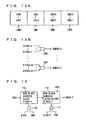
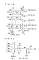
- Fig. 12 is a schematic representation of an arrangement of a data mask instruction signal generating portion.
- the data mask instruction signal generating portion includes mask input (Min) buffers 7a to 7d respectively taking in data mask signals M0 to M3 provided externally in synchronization with clock signal CLK, data mask (DM) latches 8a to 8d provided corresponding to the respective mask buffers for latching output signals from mask input buffers 7a to 7d according to data mask latch instruction signal DML, a 4:1 multiplexer 9 for selecting one of output signals from mask input buffers 7a to 7d according to spare data mask selecting signals SDMSEL0 to SDMSEL3 from column redundancy control circuit CRC shown in Fig.
- DM latch 8s for latching an output signal from multiplexer 9 according to data mask latch instruction signal DML.
- DM latches 8a to 8d output the data mask instruction signals /DM0 to /DM3, and DM latch 8s outputs a spare data mask instruction signal /DMS.
- Data mask latch instruction signal DML is generated at a prescribed timing in synchronization with clock signal CLK in a data write operation.
- Fig. 13A shows the correspondence between data mask instruction signals /DM0 to /DM3 and write data bus line pairs IOW0 to IOW31.
- data mask instruction signals /DM0 to /DM3 each mask 8 bits of data.
- Data mask instruction signals /DM0, /DM1, /DM2, and /DM3 correspond to write data bus line pairs IOW0 to IOW7, IOW8 to IOW15, IOW16 to IOW23, and IOW24 to IOW31, respectively.
- spare data mask selecting signals SDMSEL0 to SDMSEL3 are generated.
- Fig. 13B is a schematic representation of an arrangement of a spare data mask selecting signal generating portion contained in column redundancy control circuit CRC.
- the spare data mask selecting signal generating portion includes OR gates OG0 to OG3 each for receiving eight adjacent spare data line selecting signals.
- OR gate OG0 receives spare data line selecting signals SIOSEL0 to SIOSEL7 to generate a spare data mask selecting signal SDMSEL0.
- OR gate OG3 receives spare data line selecting signals SIOSEL24 to SIOSEL31 to generate a spare data mask selecting signal SDMSEL3.
- the OR gate not shown in Fig. 13B also, receives spare data line selecting signals by a unit of 8 bits and generates a corresponding spare data mask selecting signal.
- 8-input OR gates are utilized in the arrangement shown in Fig. 13B.
- the decoding operation of an address designating a data line to be replaced is performed upon the generation of spare data line selecting signals SIOSEL0 to SIOSEL31, so that the decoding operation may be utilized in generating the spare data mask selecting signals.
- Fig. 14 is a schematic representation of an arrangement of a portion that generates a row block address signal provided to a column redundancy control circuit.
- the row block address signal generating portion includes an AND circuit 10b for receiving an array activating instruction signal ⁇ ACT and a row bank address RBK, a row block address latch circuit 10a for taking in and latching a row block address signal RBA at the activation of an output signal from AND circuit 10b, an AND circuit 11b for receiving a column access operation instruction signal ⁇ COLA and a column bank address signal CBK, and a row block address latch output circuit 11a for outputting as row block address signals RBA0 to RBA3 a row block address signal that is taken in and provided from row block address latch circuit 10a together with a page selecting signal PGS during the activation of an output signal of AND circuit 11b.
- Array activating instruction signal ⁇ ACT is activated when a row access command is provided and remains activated for a prescribed period of time.
- Row bank address RBK designates a bank to be accessed in a row access. There are two banks in the present embodiment, and when the bank related to the control signal generating portion is specified, the output signal of AND circuit 10b attains the active state.
- Row block address signal RBA provided to row block address latch circuit 10a designates one of the eight row blocks, since there are two pages, and, for instance, the row blocks of the same position in each of the pages are designated.
- a row access is performed with a page being a unit, a page address and a row block address are provided, and the word line selection is performed individually for each page.
- Column access instruction signal ⁇ COLA is driven to the active state when a read command or a write command is provided.
- Column bank address signal CBK is provided simultaneously when the read command or the write command is provided, and designates one of the two banks.
- Row block address latch output circuit 11a is activated when the column access instruction is provided and when the related bank is designated by the column bank address, and outputs row block address signal RBA latched and outputted by row block address latch circuit 10a along with page selecting signal PGS.
- Row block address signals RBA0 to RBA3 from row block address latch output circuit 11a are 4 bits, while row block address signal RBA provided to row block address latch circuit 10a are 3 bits (excluding the page address).
- Row block address latch output circuit 11a adds page selecting signal PGS in the most significant bit position of row block address signal RBA to generate the 4-bit row block address signals RBA0 to RBA3. Thus, one of the 16 row blocks is specified.
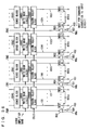
- Fig. 15 is a schematic representation of an arrangement of a spare data line selecting signal generating portion of a column redundancy control circuit shown in Fig. 7.
- column redundancy control circuit CRC includes a block decoder 12 activated in response to a spare block decode enable signal SBDE for decoding row block address signals RBA0 to RBA3 to generate a block selecting signal BS ⁇ 0:15>; program circuits 13a to 13e, including fuse circuits H0 to H15 provided corresponding to the respective row blocks, for storing an address of a defective data line pair; multiplexers (MUX) 14a to 14e provided corresponding to the respective program circuits 13a to 13e for selecting an output of a fuse circuit of a corresponding program circuit according to block selecting signal BS ⁇ 0:15> from block decoder 12; a program circuit 15, including fuse circuits H0 to H15 correspondingly provided to the respective row blocks, for storing information indicating whether or not to replace a defective data line for each row block; a multiplexer (
- Fuse circuits H0 to H15 store a one-bit address. By decoding the storage contents of the fuse circuits of program circuits 13a to 13e in the same row block, defective data line address signal of 5 bits RPA0 to RPA4 is generated. Fuse circuits H0 to H15 in program circuit 15 store information on whether or not to perform the replacement for defect in the respective row blocks.
- a specific arrangement of fuse circuits H0 to H15 is simply required to be capable of storing one bit of address by a fuse program, and the well known arrangement of a fuse program circuit that generates a signal instructing a specified operation mode by fixing the potential of a pad, for example, can be utilized.
- Column redundancy control circuit CRC varies the timing at which spare data line selecting signals SIOSEL0 to SIOSEL31 are set to the definite state for a data write and for a data read.
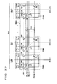
- Fig. 16 is a schematic representation of an arrangement of a portion that generates a spare block decode enable signal SBDE shown in Fig. 15.
- a spare block decode enable signal generating portion includes a command decoder 18 for taking in commands READ and WRITE provided externally in synchronization with clock signal CLK to generate a read operation instruction signal ⁇ re and a write operation instruction signal ⁇ wr, a delay circuit 19 for delaying read operation instruction signal ⁇ re from command decoder 18 by a prescribed period of time, an OR circuit 20 for receiving an output signal of delay circuit 19 and write operation instruction signal ⁇ wr from command decoder 18, and a decode control circuit 21 for generating, according to an output signal from OR circuit 20 and a column bank address signal CBK, the spare block decode enable signal SBDE that remains activated for a prescribed period of time.
- Command decoder 18 drives read operation instruction signal ⁇ re to the active state when read command READ is provided, and drives write operation instruction signal ⁇ wr to the active state when write command WRITE is provided.
- Decode control circuit 21 is activated when column bank address signal CBK is designating a corresponding bank, and holds spare block decode enable signal SBDE in the active state for a prescribed period of time according to the activation of an output signal from OR circuit 20.
- the timing at which block selecting signal BS ⁇ 0:15> from block decoder 12 is generated in a data read operation is delayed from that in a data write operation.
- spare determination is performed at an early time and an internal write data provided from an input buffer is selected by a spare multiplexer SMUX (see Fig. 7), so that the write driver can be activated at an earlier timing.
- spare data line selecting signal SIOSEL needs only be driven to the definite state before the preamplifier output is made definite so that a spare data line selecting signal can be generated based on the spare determination and the result of the determination well in time even with delay circuit 19, and thus, the defect repair can be performed well in time.
- Fig. 17 is a diagram showing a modification of column redundancy control circuit CRC.
- spare data line selecting signals SIOSEL0 to SIOSEL31 from decode latch circuit 17 are provided to spare multiplexer SMUX shown in Fig. 7 as spare write data line selecting signals WSIOSEL0 to WSIOSEL31.
- spare data line selecting signals SIOSEL0 to SIOSEL31 from decode latch circuit 17 shown in Fig. 15 are provided via delay circuit 22 to multiplexers MUX0 to MUX 31 for selecting a preamplifier output shown in Fig. 7 as spare read data line selecting signals RSIOSEL0 to RSIOSEL31.
- spare block decode enable signal SBDE is activated at the same timing for a data read and a data write, and delay circuit 19 of the circuit shown in Fig. 16 is removed.
- a write data line to be replaced can be selected at an early timing during a data write operation.
- Fig. 18 is a timing diagram representing an example of operation waveform when the timing at which the result of the spare determination is obtained is varied for a read mode and for a write mode.
- row address signals RBA0 to RBA3 are driven to the definite state according to column bank address signal CBK. Then, in a write mode, column redundancy control circuit CRC performs the decoding operation at an early timing and drives spare data line selecting signals SIOSEL0 to SIOSEL31 (WSIOSEL0 to WSIOSEL31) to the definite state.
- read command READ is provided at time T2 and time T3.
- the time required until output data PAO0 to PAO31 and PAOS are output is determined by the memory array arrangement.
- preamplifier activating signal PAE is activated and output data PAO0 to PAO31 and PAOS are made definite
- spare data line selecting signals SIOSEL0 to SIOSEL31 (RSIOSEL0 to RSIOSEL31) from the column redundancy control circuit are driven to the definite state. Therefore, the time during which the output signals of multiplexers MUX0 to MUX31 are in the indefinite state can be shortened, and the malfunctioning of an internal circuit due to an invalid data signal is prevented. In addition, the current consumed by the charging and discharging of a signal line due to the invalid data can be reduced.
- the arrangement of differencing the timing of spare determination for a data write and for a data read may be applied to the arrangement in which defective bit repair is performed by replacing the defective data line in the arrangement in which a common data line transmits read data and write data, to achieve the similar effect.
- a defective replacement read/write data line address is programmed by a fuse circuit provided to each of the row blocks.
- Defective replacement read/write data line address for a multiple of (for instance, two) row blocks may be programmed in a fuse circuit.
- a fuse circuit may be provided in common to a read data line pair and a write data line pair, while a spare determination circuit (MUX16 and a decoder latch circuit) may be provided separately for a read data line pair and a write data line pair.
- a read data bus and a write data bus are provided separately and the spare determination operation is done at different timing in a read operation mode and in a write operation mode, so that the data read operation can be performed before the data lines are fully equalized after the data write operation.
- the spare determination operation is done at different timing in a read operation mode and in a write operation mode, so that the data read operation can be performed before the data lines are fully equalized after the data write operation.
- Fig. 19 is a schematic representation of an arrangement of a DRAM macro array portion according to a second embodiment of the present invention.
- a sense amplifier band SB# is arranged between the row blocks.
- a read data line pair IOR and a write data line pair IOW are provided in parallel in the column direction over the memory cell array.
- a read data line pair and a write data line pair are indicated by the same interconnection line.
- Write data mask lines /DM0 to /DM15 each are provided corresponding to the 8-bit read data line pairs and write data line pairs.
- a spare read data line pair SIOR and a spare write data line pair SIOW are provided for 32-bit read data line pairs and write data line pairs.
- Data mask lines /DM0 to /DM15 are provided in the same interconnection layer as these read data line pairs IOR and write data line pairs IOW or in an upper layer.
- Data mask lines /DM0 to /DM15 include a global mask line GM that extends along the column direction and a local data mask line LM provided corresponding to 8-bit sense amplifier circuits in each sense amplifier band SB#. In a column select operation, all local data mask signals are driven in each column block. Thus, a data mask signal is set to a data write inhibiting state or a data write permitting state according to a mask instruction signal M even in a non-selected row block.
- Fig. 20 is a diagram representing an arrangement of a portion related to one sense amplifier circuit.
- a write gate WG includes transfer gates TGa and TGb rendered conductive in response to a signal on a write column select line CSLW, and transfer gates TMa and TMb connected in series to transfer gates TGa and TGb for receiving a write data mask signal /DM at their respective gates.
- Other parts of the arrangement are the same as those shown in Fig. 6, and the same reference characters are provided to the corresponding parts. Detailed description relating to these corresponding parts is not repeated here.
- transfer gates TGa and TGb are connected to write data lines IOWL and /IOWL, and transfer gates TMa and TMb receiving write data mask signal /DM at the control gates thereof are connected to a sense amplifier circuit.
- Write data mask signal /DM is at the "H" level when a data write is permitted, and is at the "L” level when the data write is inhibited. Therefore, even when write data mask signal /DM is set to the state indicating a data write, if write column select line CSLW is in the non-selected state, transfer gates TGa and TGb are in the non-conductive state.
- the load on write data lines IOWL and /IOWL is only the source junction capacitances of transfer gates TGa and TGb of write gate WG.
- transfer gates TMa and TMb are connected to write data lines IOWL and /IOWL, diffusion capacitances of transfer gates TMa and TMb and source diffusion capacitance of transfer gates TGa and TGb would be connected to the write data lines in a data write, causing a greater load for a write driver.
- a plurality (18 per bank) of sense amplifier circuit groups SAG are provided corresponding to write data line pair IOW.
- Each sense amplifier circuit group SAG includes eight sense amplifier circuits. One of the eight sense amplifier circuits is selected by a write column select line.
- a transfer gate receiving write column select signal CSLW is connected to write data line pair IOW in write gate WG.
- source diffusion capacitance Cl of a transfer gate coupled to a write column select line is only connected to write data line pair IOW in a non-selected sense amplifier circuit group.
- Line capacitance Cg is connected to write data line pair IOW.
- write driver WDV only drives parasitic capacitances Cg and Cl, so that write data line pair IOW can be driven at a high speed.
- a transfer gate receiving data mask signal /DM in a write gate is connected to a write data line pair, when data write is permitted, source diffusion capacitance and drain diffusion capacitance of a transfer gate receiving mask data as well as source diffusion capacitance of a transfer gate coupled to a write column select line would contribute as capacitance Cl so that the capacitance value becomes greater, and the driving load of write driver WDV becomes greater.
- the diffusion capacitance of the transfer gate receiving the data mask signal can be hidden away from write driver WDV by a transfer gate coupled to a non-selected write column select line so that the load of write driver WDV is alleviated, and a high-speed data write operation is achieved.
- a period tRCD between the dispatch of a bank activation command (ACT) and the time when a column-related command can be dispatched in a mask write operation can be shortened as will be described below.
- Fig. 22A is a diagram showing the signal waveforms in the case in which only transfer gates TGa and TGb shown in Fig. 6 are included as write gate WG.
- ROWACT row access command
- the voltage level of a selected word line WL in a selected row block rises at time tWL.
- memory cell data is read on bit lines BL and BL.
- Fig. 22A shows a signal waveform of the case where "L" level data is read on bit line BL.
- An N sense amplifier (or a sense amplifier formed by an N-channel MOS transistors) of a sense amplifier circuit is activated at time tSON, and thereafter, a P sense amplifier (or a sense amplifier formed by P-channel MOS transistors) of a sense amplifier circuit is activated at time tSOP, thereby the voltage levels of bit lines BL and BL are respectively amplified to "L" level and "H” level according to the data.
- write column select line CSLW is activated at time tCSLW when a column access command COLACT (write command) is provided.
- Write data line IOWL is already precharged to sense power supply voltage VccS by a write driver.
- write driver WDV is set to the output high impedance state (see Fig. 9).
- the precharged voltage of the write data line is accumulated in parasitic capacitances Cg and Cl shown in Fig. 21, and when a write gate is formed only of a pair of transfer gates, the electrical charge stored in the parasitic capacitance flows in from the write data line when write column select line CSLW is activated and the voltage level of bit line BL rises. Since, however, the sensing operation by the sense amplifier circuit is complete and the sense amplifier is in the latching state, even when the "L" level potential rises, it is discharged by the sense amplifier circuit so that the data is not destructed.
- write column select line CSLW may be activated before the completion of the sense amplifier operation. Since the sense amplifier operation is not completed, the voltage level of a sense node of the sense amplifier circuit rises due to the electrical charge flowing in from the parasitic capacitance of the write data line.
- data mask signal /DM is at the "L" level so that transfer gates TMa and TMb attain the non-conductive state, and no electrical charge flows into sense nodes of a sense amplifier circuit from the write data lines when a data write is masked.
- Fig. 23 is a diagram showing a first modification of the second embodiment of the present invention.
- a memory cell row block is divided into a plurality of memory cell blocks along the row direction, and a sub-word line driver SWD is arranged between the memory cell blocks.
- Sense amplifier circuit groups SAG are provided for the respective memory cell blocks MCB.
- a word line has a hierarchical word line arrangement, a main word line is provided in common to row blocks, and a sub-word line is provided for each memory cell block.
- Sub-word line driver SWD is arranged in a sub-word line driver disposing region SWDR, and is shared by two memory cell blocks adjacent to one another in the row direction.
- a sub-word line driver is provided corresponding to a respective sub-word line, and a main word line is disposed to a corresponding to a prescribed number of sub-word lines.
- Each sub-word line driver drives a corresponding sub-word according to at least the signal potential on the corresponding main word line.
- an arrangement may be used in which a sub-word line driver drives a corresponding sub-word line to the selected state according to a signal on a main word line and a sub-word line selecting signal (when multiple sub-word lines are provided corresponding to one main word line).
- sub-word line driver disposing region SWDR a sub-word line driver is disposed, but no memory cell nor sense amplifier circuit is arranged.
- Data mask lines /DM0 to /DM15 are respectively arranged in sub-word line driver disposing region SWDR.
- a read data bus and a write data bus are shown together as a composite data bus DBL.
- Each of data mask lines /DM0 to /DM15 are provided corresponding to an 8-bit read/write data bus DBL.
- a sense power supply line for transmitting sense amplifier power supply voltage VccS and ground voltage Vss is provided in this free region of the memory cell block, in the same layer as the read data bus and the write data bus or in an upper layer, to supply sense power supply voltage stably to each sense amplifier circuit.
- the regions receiving data mask signals /DMs0 to /DMs3 shown by the dotted lines within the memory cell blocks indicate spare column regions.
- Fig. 24 is a diagram representing an arrangement of a second modification of the second embodiment of the present invention.
- An arrangement of write driver WDV (or spare write driver SWDV) shown in Fig. 24 includes an inverter 25 for inverting internal write data WDD, a CMOS inverter circuit 26a for driving write data line IOWL according to an output signal of inverter 25, and a CMOS inverter circuit 26b for driving a complementary write data line /IOWL according to internal write data WDD.
- Write driver WDV (or spare write driver SWDV) shown in Fig. 24 is a bi-state buffer that two-value-drives write data lines IOWL and /IOWL (driving to H or L level, normally), and has no output high impedance state.
- CMOS inverters 26a and 27b operate using the voltage having the same voltage level as sense power supply voltage VccS as the operation power supply voltage. No problem arises even when using such a two-value driving write driver, as described below with reference to Fig. 25.
- write column select line CSLW When a data write is not performed (during a read operation or in a standby state), write column select line CSLW is in the inactive state, and transfer gates TGa and TGb are in the non-conductive state so that sense amplifier circuit SA is disconnected from write data lines IOWL and /IOWL, as can be seen from Fig. 25.
- write mask signal /DM When a data write is masked during the data write, write mask signal /DM is in the active state, and transfer gates TMa and TMb are in the non-conductive state so that sense amplifier circuit SA is disconnected from write data lines IOWL and /IOWL. Consequently, during the write mask, there is no need to equalize the potentials of write data lines IOWL and /IOWL since sense amplifier circuit SA is disconnected from write data lines IOWL and /IOWL.
- the original purpose of the equalizing operation is to prevent the writing of uncertain data by transmission of the potential difference between the write data lines to the sense amplifier circuit while the write driver is in the output high impedance state.
- sense amplifier circuit SA When a data write is not performed, however, sense amplifier circuit SA is disconnected from write data lines IOWL and /IOWL. Thus, there is no need for an equalizing operation, and no problem arises even when the write data lines are two-value driven.
- the use of write driver enable signal WDE and equalizing signal /IOWEQ is no longer necessary.
- the data write time is determined only by the active period of write column select line CSLW, as shown in Fig. 26.
- the time period for equalizing write data lines IOWL and /IOWL, or the precharging period, is no longer necessary so that a shorter write cycle time and a high operation frequency of the data write are achieved.
- Fig. 27 is a diagram representing a third modification of the second embodiment of the present invention.
- the write driver receives an external power supply voltage Vcc as the operation power supply voltage.
- CMOS inverter circuits 26a and 26b are shown in Fig. 27, inverter 25 shown in Fig. 24 also receives external power supply voltage Vcc as the operation power supply voltage.
- Data mask signal /DM is set to the voltage level having the same amplitude as sense amplifier power supply voltage VccS. Thus, data mask signal /DM varies between ground voltage Vss and sense power supply voltage VccS.
- write column select signal CSLW has its amplitude set at external power supply voltage level, and is changed between ground voltage Vss and external power supply voltage Vcc.
- Transfer gates TGa and TGb are activated in write gate WG when a data write is performed.
- write column select line CSLW is in the inactive state, and transfer gates TGa and TGb are in the non-conductive state.
- data mask signal /DM is at ground voltage Vss level, and transfer gates TMa and TMb are in the non-conductive state.
- sense amplifier circuit SA is disconnected from write driver WDV or the spare write driver.
- data mask signal /DM is set at sense power supply voltage VccS level.
- a case is considered in which a voltage (2.5 V) of external power supply voltage Vcc level is transmitted according to write data on write data line IOWL.
- the voltage of a gate of transfer gate TMa in write gate WG is at sense power supply voltage VccS level, i. e. 2.0 V.
- Sense node SNa of sense amplifier circuit SA attains "H" level according to the "H" level data from the write driver. After a signal having a lower voltage level than 2.0 V is transmitted to the sense node due to the loss of threshold voltage of transfer gate TMa, sense node SNa is held at sense power supply voltage 2.0 V level by sense amplifier circuit SA.
- transfer gate TMa If the threshold voltage of transfer gate TMa is greater than 0.5 V, no current flows in this state via transfer gate TMa.
- transfer gate TMa has its gate and its source interconnected, and attains a state equivalent to a PN diode so that it becomes non-conductive.
- Fig. 29 is a diagram representing an example of a power supply configuration. This power supply configuration is utilized in the first embodiment or the second embodiment.
- write driver group WDG in a data path DP receives as an operation power supply voltage a power supply voltage VccS from a voltage down converter VDC for down-converting external power supply voltage Vcc1.
- Power supply voltage VccS from voltage down converter VDC is also utilized as power supply voltage for driving a sense amplifier circuit inside a memory cell array MA.
- a decode circuit XYD for selecting a memory cell in memory cell array MA is provided with an external power supply voltage Vcc2 and a boosted voltage Vpp from a boosting circuit BST for boosting external power supply voltage Vcc1.
- Boosted voltage Vpp is used to drive a word line.
- External power supply voltage Vcc2 is for example 2.5 V
- external power supply voltage Vcc1 is for example 3.3 V.
- external power supply voltage Vcc2 is provided as operation power supply voltage to logic circuit LG, a latch/buffer group contained in data path DP, and control circuit CG.
- the write driver only drives the write data line up to sense power supply voltage level so that a data line amplitude greater than necessary is not created.
- write driver group WDG In write driver group WDG, however, 128 write drivers are provided for each memory cell array, and the total of 256 bits of write drivers operate simultaneously.
- sense power supply voltage VccS may be significantly lowered so that an accurate data write cannot be performed (i. e. destruction of normal memory cell data caused by malfunctioning of the sense amplifier circuit due to sense power supply noise).
- the sense amplifier circuit consumes a large amount of current during this operation, as far as the power supply voltage becomes stable within a prescribed period, the sense amplifier circuit can sense and amplify memory cell data by accurate sensing operation.
- the response speed of voltage down converter VDC is relatively slowed, and it is possible that the drop in power supply voltage VccS cannot be sufficiently compensated for during the write operation of the write driver group.
- Fig. 30 is a diagram representing a power supply distribution according to the third modification.
- external power supply voltage Vcc2 is provided to data path DP.
- a circuit contained in data path DP operates according to external power supply voltage Vcc2.
- a write driver group also operates according to external power supply voltage Vcc2.
- Other parts of the power supply layout configuration is the same as those shown in Fig. 29.
- Fig. 31 is a diagram representing an arrangement of a preamplifier.
- a preamplifier PA includes a read data line equalizing/precharging circuit 30 activated when preamplifier activating signal PAE is deactivated, for precharging and equalizing read data lines IORL and /IORL to external power supply voltage Vcc level, a CMOS inverter latch circuit 32 activated in response to the activation of preamplifier activating signal PAE for differentially amplifying the provided data, a read data line isolating gate 31 rendered non-conductive in the activation of preamplifier activating signal PAE for disconnecting CMOS inverter latch circuit 32 and read data lines IORL and /IORL, and a flip-flop 33 for taking in an output signal of CMOS inverter latch circuit 32 in the activation of preamplifier activating signal PAE and for attaining the latching state during the deactivation of preamplifier activating signal PAE.
- Flip-flop 33 outputs output data PAO of
- CMOS inverter latch circuit 32 operates using external power supply voltage Vcc (for example, 2.5 V) as one operation power supply voltage. With the use of read data line isolating gate 31, the load on a sense node can be alleviated during the sensing and amplifying operation of CMOS inverter latch circuit 32 so that the sensing and amplifying operation can be performed at a high-speed.
- the arrangement of CMOS inverter latch circuit 32 is the same as sense amplifier circuit SA, and the small potential difference provided from read data lines IORL and /IORL is amplified at a high speed.
- Flip-flop 33 is formed of an AND circuit operating as a pass gate and an NOR circuit forming a latch circuit, and during the activation of preamplifier activating signal PAE, passes an output signal of CMOS inverter latch circuit 32 via the AND circuit and latches by the NOR circuit. When preamplifier activating signal PAE is deactivated, data is latched by the NOR circuit.
- the operation power supply voltage of preamplifier PA is external power supply voltage Vcc, and the amplitudes of read data lines IORL and /IORL attain external power supply voltage Vcc level.
- Vcc2 external power supply voltage
- a write gate is formed of a transfer gate receiving at its gate a data mask signal and a transfer gate receiving a write column select signal connected in series, the load for the write driver is alleviated and a high-speed data write becomes possible. Moreover, by utilizing a bi-state buffer as a write driver, the precharging period of the write data line is no longer required, and a shorter write cycle time is achieved.
- Vcc external power supply voltage
- Fig. 32 is a schematic representation of an arrangement of the main portion of a third embodiment of the present invention.
- write driver WDV operates using external power supply voltage Vcc as one operation power supply voltage.
- Write driver WDV has the same arrangement as that shown in the above Fig. 9, and is formed of a tristate buffer.
- Write gate WG includes transfer gates TGa and TGb receiving at their control gates a signal on write column select line CSLW.
- the signal on write column select line CSLW changes between ground voltage Vss and sense amplifier power supply voltage VccS.
- Sense amplifier circuit SA operates using as an operation power supply voltage, and drives one of sense nodes SNa and SNb to the level of sense amplifier power supply voltage VccS.
- write driver WDV attains the output high impedance state during a mask write operation, and data lines IOWL and /IOWL maintain the state of being precharged and equalized to external power supply voltage Vcc.
- the stored charge flows into the sense amplifier circuit from the parasitic capacitance of write data lines IOWL and /IOWL.
- the voltage levels of the write data lines are the same, and sense amplifier circuit SA holds the data stably if the sense amplifying operation is completed.
- the external power supply voltage is near the bit line precharge voltage level (1.0 V), so that inversion of sense amplifier data does not occur.
- write data lines IOWL and /IOWL are driven according to write data WDD.
- external power supply voltage Vcc is low, i. e. 1.2 V
- write column select signal CSLW is at the voltage level of 2.0 V of sense amplifier power supply voltage
- the "H" level of external power supply voltage Vcc can be transmitted to sense amplifier circuit SA without the threshold voltage loss across transfer gates TGa and TGb.
- charge/discharge current of the write data lines as well as power consumption can be reduced.
- Fig. 33 is a schematic representation of an arrangement of a modification of the third embodiment according to the present invention.
- an AND circuit AG for receiving write column select signal CSLW and data mask signal /DM is provided for write gate WG.
- AND circuit AG operates using sense amplifier power supply voltage VccS as one operation power supply voltage.
- Write gate WG includes transfer gates TGa and TGb for receiving at their gates an output signal of AND circuit AG.
- Write driver WDV is a bi-state buffer, and normally drives write data lines IOWL and /IOWL according to write data WDD.
- data mask signal /DM is at the "H” level
- write column select signal CSLW is also at the “H” level
- the output signal of AND circuit AG attains the "H” level
- transfer gates TGa and TGb are made to conduct.
- AND circuit AG should be arranged such that it receives data mask signal /DM and write column select signal CSLW (a signal line and a signal on the signal line are indicated by the same reference characters).
- AND circuit AG is arranged in the free region where a sense amplifier band intersects a sub-word line decoders, for instance, so that the increase in the array area can be limited while a write column select signal at sense amplifier power supply voltage VccS can be transmitted to each write gate WG.
- the power supply voltage of a write driver can be set at an external power supply voltage level lower than the sense amplifier power supply voltage, thereby significantly reducing power consumption.
- Fig. 34 is a schematic representation of an arrangement of the main portion of a semiconductor memory device according to a fourth embodiment of the present invention.
- Fig. 34 two memory cell blocks MBa and MBb and a sub-word line driver group SWDG provided between the memory cell blocks are shown.
- Sense amplifier groups SAGau and SAGal are disposed on opposite sides of memory cell block MBa in the column direction, and sense amplifier groups SAGbu and SAGbl are disposed on opposite sides of memory cell block MBb in the column direction.
- Sense amplifier activating signal SONn-1 is provided to sense amplifier circuits contained in sense amplifier groups SAGau and SAGbu.
- Sense amplifier activating signal SONn is provided to sense amplifier circuits contained in sense amplifier groups SAGal and SAGbl.
- Read data line pairs IOR(m ⁇ 8+6) and IOR(m ⁇ 8+7) and write data line pairs IOW(m ⁇ 8+6) and IOW(m ⁇ 8+7) are disposed on memory cell block MBa.
- m 0 to 15.
- Signal lines for transmitting data mask signals /DMm and /DM(m+1) and a spare data mask signal /DMsk are provided over the region where sub-word line driver SWD is provided.
- a spare read data line pair SIORk and a spare write data line pair SIOWk as well as write data line pairs IOW((m+1) ⁇ 8)and IOW((m+1) ⁇ 8+1), and read data line pairs IOR((m+1) ⁇ 8) and IOR((m+1) ⁇ 8+1) are provided.
- An AND circuit for receiving the data mask signal and the sense amplifier activating signal to generate a local data mask signal is arranged in the portion where a sub-word line driver group SWDG disposing region intersects a sense amplifier group disposing region.
- an AND circuit 40a for receiving sense amplifier activating signal SONn-1 and data mask signal /DMm is provided for sense amplifier groups SAGau
- an AND circuit 40b for receiving sense amplifier activating signal SONn and data mask signal /DMm is provided for sense amplifier groups SAGal.
- an AND circuit 40c for receiving sense amplifier activating signal SONn-1 and spare data mask signal /DMsk as well as an AND circuit 40d for receiving sense amplifier activating signal SONn-1 and data mask signal /DM(m+1) is provided.
- an AND circuit 40e for receiving spare data mask signal /DMsk and sense amplifier activating signal SONn as well as an AND circuit 40f for receiving sense amplifier activating signal SONn and data mask signal /DM(m+1) is provided.
- Each of these AND circuits 40a to 40f receives sense amplifier power supply voltage VccS as one operation power supply voltage. Moreover, local data mask signals from these AND circuits 40a to 40f are provided to write gates (64 write gates) corresponding to 8-bit write data line pairs IOW arranged for the corresponding sense amplifier groups.
- Signal lines for transmitting data mask signal /DM (representing data mask signals /DM0 to /DM15) extending in the column direction are provided in common to the memory cell blocks in a corresponding column block.
- Sense amplifier activating signals SONn-1 and SONn are driven to the active state in the activation of a corresponding row block.
- a column is accessed for data writing in the row block in the active state.
- sense amplifier activating signal SONn-1 is in the inactive state
- sense amplifier groups SAGau and SAGbu are inactive
- memory cell blocks MBa and MBb are in the non-selected state (precharged state). Therefore, column access is not performed for memory cell blocks MBa and MBb in this case.
- the active/inactive state of the data mask signal does not affect the write gates disposed in sense amplifier groups SAGau and SAGbu (since a write column select signal maintains the inactive state).
- disabling AND circuits 40a, 40c, and 40d by sense amplifier activating signal SONn-1 eliminates the need to drive a data mask signal for a non-selected row block so that the power consumed by the drive circuit that drives the data mask signal can be saved.
- Fig. 35 is a schematic representation of an arrangement of a portion related to one data mask signal /DM.
- 16 memory cell blocks MCB0 to MCB15 are disposed in alignment in the column direction.
- Data mask signal /DM from a DM latch 8 is provided in common to eight data write line pairs (8IOs) of these memory cell blocks MCB0 to MCB15.
- DM latch 8 operates using sense amplifier power supply voltage VccS as one operation power supply voltage.
- AND circuits 40-0 to 40-17 are provided corresponding to the respective memory cell blocks MCB0 to MCB15.
- Sense amplifier activating signals SON0 to SON17 are provided to the respective AND circuits 40-0 to 40-17.
- sense amplifier activating signals SON1 and SON2 applied to the sense amplifier bands provided on either side of memory cell block MCB1 are in the active state, and the remaining sense amplifier activating signals SON0 and SON3 to SON17 are in the inactive state. (Here, only the one-page operation is considered.)
- AND circuits 40-0, 40-3 to 40-17 are disabled, and local data mask signals /LDM0, /LDM3 to /LDM17 are all in the inactive state or at the "L" level, so that write gates are all in the non-conductive state.
- Local data mask signals /LDM1 and /LDM2 from AND circuits 40-1 and 40-2 are driven to the active state or the inactive state according to data mask signal /DM.
- DM latch 8 is only required to drive a data mask signal line (global data mask line) existing in the column direction so that its load is alleviated.
- AND circuits 40-0 to 40-17 respectively operate using sense amplifier power supply voltage VccS as one operation power supply voltage as shown in Fig 34, two local data mask signals /LDM1 and /LDM2 are only charged/discharged for one row block, so that the consumed current of sense amplifier power supply voltage VccS can be reduced.
- DM latch 8 is not required to drive data mask signal lines arranged for all row blocks but required to drive a global data mask line in the column direction only, so that the data mask signal can be set to the definite state at a high speed.
- a sense amplifier activating signal for the two row blocks is driven to the active state.
- the column select operation is performed for one row block, the data mask signal, therefore, is required to drive local data mask lines for these two activated row blocks.
- the charge/discharge current is lower in comparison with the arrangement in which a data mask signal is driven for all row blocks, and consequently, the consumed current of the sense amplifier power supply voltage is reduced.
- write driver WDV is formed by a bi-state buffer that receives external power supply voltage Vcc as one operation power supply voltage.
- External power supply voltage Vcc is utilized as the operation power supply voltage for DM latch 8 (shown in parentheses in Fig. 35) and sense amplifier power supply voltage VccS is provided as the operation power supply voltage to AND circuits 40-0 to 40-19, thereby reducing the consumed current of sense amplifier power supply voltage VccS.
- the provision of a level converting function to AND circuits 40-0 to 40-19 can cope with the situation where the voltage level of external power supply voltage Vcc is lower than sense amplifier power supply voltage VccS.
- Data mask signal /DM designates a write mask operation that allows a data write when at the "H” level and inhibits the data write when at the "L” level.
- NOR gates are used instead of AND circuits 40-0 to 40-17, and a sense amplifier activating signal SOP for activating a P sense amplifier is used as a sense amplifier activating signal. Consequently, even when a data mask signal is a positive logic signal, a data mask signal transmission line can be divided into a global mask data line and a local data mask line.
- the data mask signal can be driven to the definite state, and in conjunction with the arrangement utilizing a bi-state buffer as a write driver, the write operation can be performed at a high speed and with low current consumption.
- a write mask gate is connected in series to a column select gate as shown in Fig. 20 et. seq. so that the write data can be masked accurately.
- a write driver can be implemented as a bi-state driver, and there is no need for a precharging operation of an internal write data line. Application of this configuration provided with such a write mask gate to different data bit widths is now considered.
- Fig. 36 is a schematic representation of an arrangement of a main portion of a semiconductor memory device (DRAM macro) according to the fifth embodiment of the present invention.
- Fig. 36 does not show a spare circuit and a latch circuit in a data path.
- An arrangement of a portion corresponding to IO data line pairs IO0 to IO31 of 32 bits is shown in Fig. 36.
- sense blocks SB#0 to SB#3 each having a prescribed number of sense amplifier circuits are disposed in a sense amplifier band.
- eight sense amplifier circuits are arranged for each IO data line pair so that the total of sixty-four sense amplifier circuits are provided. Eight sense amplifier circuits form one sense amplifier unit, as will be described below.
- Column select blocks CSB#0 to CSB#3 for selecting sense amplifier circuits contained in the corresponding sense blocks SB#0 to SB#3 in response to a column select signal CSLG on a column select line group are provided corresponding to sense blocks SB#0 to SB#3.
- Each of column select blocks CSB#0 to CSB#3 selects eight sense amplifier circuits from a corresponding one of sense blocks SB#0 to SB#3 according to column select signal CSLG on the column select line group and couples the eight sense amplifier circuits to the corresponding 8-bit IO data line pairs.
- Write mask circuits WM#0 to WM#3 for inhibiting the connection between the corresponding IO data line pairs and sense blocks in response to the respective write mask instruction signals /DM0 to /DM3 are disposed between sense blocks SB#0 to SB#3 and column select blocks CSB#0 to CSB#3.
- Each of write mask circuits WM#0 to WM#3 inhibits the data write operation with eight IO data line pairs being a unit, as in the previous first embodiment.
- Write drivers WDV0 to WDV31 for generating internal write data according to received data D for transmission to the corresponding IO data line pairs when activated are provided corresponding to IO data line pairs IO0 to IO31.
- IO data line pairs IO0 to IO31 are internal data line pairs for transmitting both write data and read data. For simplicity, no preamplifier circuit is shown in the figure.
- Write drivers WDV0 to WDV31 are divided into write driver blocks corresponding to write mask circuits WM#0 to WM#3, and activation and inactivation are controlled on a block basis.
- Write drivers WDV0 to WDV7 are activated when a write driver enable signal WDEa is activated, and write drivers WDV8 to WDV15 are activated when a write driver enable signal WDEb is activated.
- Write drivers WDV16 to WDV23 are activated when a write driver enable signal WDEc is activated, and write drivers WDV24 to WDV31 are activated when a write driver enable signal WDEd is activated.
- Write driver enable signals WDEa to WDEd are generated based on a data line selecting address according to the input/output data bit width.
- Inverter circuits VG0 to VG3 for receiving internal data line selecting signals YD0 to YD3, and NOR (mask gate) circuits MG0 to MG3 for receiving write mask instructions WMa to WMd and output signals from inverter circuits VG0 to VG3 to generate write mask instruction signals /DM0 to /DM3 respectively are provided for the respective write mask circuits WM#0 to WM#3.
- Data line selecting signals YD0 to YD3 are generated according to a column address signal corresponding to the write data bit width.
- the correspondence between write mask instruction applied from an outside and internal mask instructions DMa to DMd is changed according to the write data bit width.
- output signals from NOR circuits MG0 to MG3 attain the "L” level
- write mask instruction signals /DM0 to /DM3 attain the "L” level of the active state so that write mask circuits WM#0 to WM#3 enter the write mask state. Consequently, the connection of a non-selected IO data line pair to a sense block is inhibited so that transmission of the precharge voltage of the IO data lines to sense blocks SB#0 to SB#3 is prevented, and the write data can be accurately written into a selected memory cell even when the input data bit width is changed.
- Fig. 37 is a schematic representation of an arrangement of a portion related to one sense block SB#i.
- sense block SB#i includes sense amplifier units SU#0 to SU#7 provided corresponding to 8-bit IO data line pairs IO ⁇ 8i> to 10 ⁇ 8i+7>.
- Each of sense amplifier units SU#0 to SU#7 includes n sense amplifier circuits SA0 to SA (n-1).
- a write mask circuit WM#i provided corresponding to sense block SB#i includes write mask gates TGM provided corresponding to sense amplifier circuits SA0 to SA (n-1) contained in each of sense amplifier units SU#0 to SU#7.
- a write mask gate TGM is rendered non-conductive when a write mask instruction signal /DMi is activated (or is at the "L" level), and disconnects sense block SB#i from IO data line pairs IO ⁇ 8i> to IO ⁇ 8i+7> regardless of the state of a column select signal CSLG.
- Column select block CSB#i includes column select units CSU#0 to CSU#7 provided corresponding to sense amplifier units SU#0 to SU#7.
- Each of column select units CSU#0 to CSU7 includes column select gates CG0 to CG (n-1) provided corresponding to sense amplifier circuits SA0 to SA (n-1) contained in a corresponding sense amplifier unit, for connecting the corresponding sense amplifier circuits to the corresponding IO data line pairs in response to selected column designating signals CSL ⁇ 0> to CSL ⁇ n-1>.
- These selected column designating signals CSL ⁇ 0> to CSL ⁇ n-1> form a column select signal group CSLG and are provided in common to sense blocks contained in a sense amplifier band.
- write mask instruction signal /DMi is provided only to a write mask circuit WM#i provided corresponding to sense block SB#i, and the mask control of a data write operation on a sense block basis is performed.
- Fig. 38 is a schematic representation of an arrangement in which data are written in parallel to all of IO data line pairs IO0 to IO31.
- data input circuits DIK0 to DIK31 are provided corresponding to write drivers WDV0 to WDV31.
- Mask input circuits MIK0 to MIK3 are provided corresponding to mask gate (NOR) circuits MG0 to MG3.
- Input circuits DIK0 to DIK31 and input circuits MIK0 to MIK3 take in data D0 to D31 and data mask instruction signals M0 to M3 in synchronization with a clock signal CLK.
- a write driver enable signal WDE0 is applied to write drivers WDV0 to WDV7, and a write driver enable signal WDE1 is applied to write drivers WDV8 to WDV15.
- a write driver enable signal WDE2 is applied to write drivers WDV16 to WDV23, and a write driver enable signal WDE3 is applied to write drivers WDV24 to WDV31.
- IO data line pairs IO0 to IO31 are simultaneously selected. Consequently, internal data line selecting signal YD0 to YD3 all attain the selected state, and output signals from inverter circuits VG0 to VG3 attain the "L" level.
- Mask gate circuit MG0 to MG3 generate write mask instruction signals /DM0 to /DM3 according to data mask instruction signals M0 to M3 received from mask input circuits MIK0 to MIK3.
- corresponding write mask circuits WM#0 to WM#3 are in the conductive state when data mask instruction signals /DM0 to /DM3 are in the non-selected state so that IO data line pairs IO0 to IO31 are connected to sense blocks SB# to SB#3 via the respective column select blocks CSB#0to CSB#3.
- write driver enable signals WDE0 to WDE3 are all driven to the active state according to a write driver enable signal WDE, and write drivers WDV0 to WDV31 are activated at the same time.
- Fig. 39 is a schematic representation of an arrangement of a write driver enable signal generating portion.
- AND gates ANG0 to ANG3 each receiving a peripheral power-supply voltage VccP at both inputs, to generate an IO data line pair selecting signal are provided.
- AND gate ANG0 corresponds to column address bits /CA0 and /CA1 and generates an internal data line selecting signal YD0.
- AND gate ANG1 corresponds to column address bits CA0 and /CA1 and generates an internal data line selecting signal YD1.
- AND gate ANG2 corresponds to column address bits /CA0 and CA1 and generates an internal data line selecting signal YD2.
- AND gate ANG3 corresponds to column address bits CA0 and CA1 and generates an internal data line selecting signal YD3.
- Write driver enable signals WDE0 to WDE3 are generated by AND gates ANG4 to ANG7 respectively receiving internal data line selecting signals YD0 to YD3 output from AND gates ANG0 to ANG3 and a write driver enable signal WDE.
- Fig. 40 is a schematic representation of an arrangement where the data bit width is reduced to one-fourth of its original size.
- data input circuits DIK0 to DIK7 are provided corresponding for write data D0 to D7 of 8 bits, and a mask input circuit MIK is provided for receiving a mask instruction signal M.
- Data input circuits DIK0 to DIK7 are coupled in parallel to write drivers WDV0 to WDV7, and are connected in parallel to write drivers WDV8 to WDV15, respectively.
- data input circuits DIK0 to DIK7 are coupled to write drivers WDV16 to WDV23 respectively, and are further coupled to write drivers WDV24 to WDV31 respectively.
- data input circuit DIK0 is coupled to four write drivers: write drivers WDV0, WDV8, WDV16, and WDV24.
- One group of IO data line pairs is selected according to internal data line selecting signals YD0 to YD3 and the data write operation is performed.
- the arrangements of other parts are the same as those shown in Fig. 38 so that the same reference characters are allocated to the corresponding parts whose descriptions are not repeated.
- an operation of a write circuit shown in Fig. 40 will be described with reference to the timing chart shown in Fig. 41.
- a write command is supplied (a write enable signal /WE is set to the active state of the "L" level), and the current column address signal Yadd is taken in, and internal data line selecting signals YD0 to YD3 are generated.
- internal data line selecting signal YD1 maintains the "H” level, while data line selecting signals YD0, YD2, and YD3 are rendered inactive.
- data input circuits DIK0 to DIK7 take in the received data in response to the rise of clock signal CLK and generates internal write data WD.
- the operation in which write data WD ⁇ 0> is generated from data data ⁇ 1> provided to an input circuit DIK0 will be discussed with reference to Fig. 41.
- Mask instruction signal M is set at the "L” level, and an internal mask instruction signal WM ⁇ 0;3> from mask input circuit MIK is at the "L” level.
- mask gate circuits MG0, MG2, and MG3 set write mask instruction signals /DM0, /DM2, and /DM3 all to the active state of the "L” level in response to the fall of internal data line selecting signals YD0, YD2, and YD3.
- write mask circuits WM#0, WM#2 and WM#3 are all rendered non-conductive, and sense blocks SB#0, SB#2 and SB#3 are disconnected from corresponding IO data line pairs IO0 to IO7 and IO16 to IO31.
- write driver enable signal WDE is activated, and write driver enable signal WDE1 for write drivers WDV8 to WDV15 is activated according to data line selecting signal YD1, and write drivers WDV8 to WDV15 drive respective IO data line pairs IO8 to IO15 according to data provided from data input circuits DIK0 to DIK7.
- Write driver WDV8 receives the write data from data input circuit DIK0 and drives IO data line pair IO8 according to write data data ⁇ 1>.
- write drivers WDV0, WDV16, and WDV24 are in the inactive state, and IO data line pairs IO0, IO16, and IO24 maintain the precharged level (power-supply voltage VccP level).
- a selected column designating signal CSL ⁇ 0> is driven to the active state, and column select gate CG0 is rendered conductive for each of sense amplifier units SU#0 to SU#7 in each of column select blocks CSB#0 to CSB#3.
- Write mask circuits WM#0, WM#2, and WM#3 are in the non-conductive state, while write mask circuit WM#1 is in the conductive state.
- write mask circuit WM#1 is in the conductive state.
- write mask circuit for a non-selected write driver block is set to the non-conductive state so that the connection of a precharged IO data line pair to a sense amplifier circuit can be prevented, and thus, change in data held by a sense amplifier circuit can be prevented.
- Fig. 42 is a diagram showing an arrangement of a write driver enable signal generating portion for the arrangement shown in Fig. 40.
- the write driver enable signal generating portion shown in Fig. 42 corresponding column address bits are applied in place of a peripheral power-supply voltage VccP, to both inputs of each of the AND gates ANG0 to ANG3.
- the arrangements of other parts is the same as those shown in Fig. 39 and the corresponding parts are denoted by the same reference characters, and their detailed descriptions will not be repeated.
- AND gates ANG0 to ANG3 each operate as a decoder, and IO data line pair selecting signal YD0 to YD3 are generated according to column address bits CA0 and CA1. Only the write driver enable signals for a selected IO data line pair group is activated.
- Fig. 43 is a schematic representation of an arrangement of a spare multiplexer SMUX shown in Fig. 7.
- the 32-bit data is reduced to the 8-bit data
- spare multiplexer SMUX includes four switching circuits SX0 to SX3.
- Internal write data WD ⁇ 0> to WD ⁇ 7> of 8 bits are supplied to each of these switching circuits SX0 to SX3.
- Switching circuit SX0 performs the selecting operation according to AND-ed signals of each of spare data line selecting signals SIOSEL0 to SIOSEL7 and data line selecting signal YD0.
- Switching circuit SX1 performs the selecting operation according to AND-ed signals of each of spare data line selecting signals SIOSEL8 to SIOSEL15 and internal data line selecting signal YD1.
- Switching circuit SX2 performs the selecting operation according to AND-ed signals of each of spare data line selecting signals SIOSEL16 to SIOSEL23 and internal data line selecting signal YD2.
- Switching circuit SX3 performs the selecting operation according to AND-ed signals of each of spare data line selecting signals SIOSEL24 to SIOSEL31 and internal data line selecting signal YD3.
- a selected IO data line pair group is designated by an internal data line selecting signal.
- Each of these spare data line selecting signals SIOSEL0 to SIOSEL31 is information including column address bits CA0 and CA1.
- IO data line pairs selected by internal data line selecting signals YD0 to YD3 contain a defective IO data line pair, the switching of IO data line pairs is performed according to switching circuits SX0 to SX3.
- an output signal from switching circuit SX attains the high impedance state.
- spare write data WDS from spare multiplexer SMUX should be set to the logic state of setting the corresponding spare write driver to the output high impedance state.
- a spare enable signal SPEN is applied to a write driver, and the write driver attains the output high impedance state when the spare is not used.
- Fig. 44 is a diagram showing an arrangement of a circuit for generating a spare data mask instruction signal.
- the arrangement shown in Fig. 44 corresponds to the arrangements shown in Figs. 12 and 15.
- the spare data mask instruction signal generating portion includes a 4:1 selecting circuit 9 for selecting internal mask instruction signals WM0 to WM3 of 4 bits generated from the mask instruction signal M according to AND-ed signals of spare data mask selecting signals SDMSEL0 to SDMSEL3 and respective internal data line selecting signals YD0 to YD3, a latch circuit 8ss for latching an output signal of 4:1 selecting circuit 9 according to a control signal DML, an inverter circuit VGS for inverting spare enable signal SPEN, and a spare mask gate circuit MSG for receiving a write data mask instruction signal DMFs from latch circuit 8ss and an output signal from inverter circuit VGS to generate a spare data mask instruction signal /DMS.
- Spare data mask instruction signal /DMS from spare mask gate circuit MSG is applied to a write mask circuit including
- spare enable signal SPEN at that time is inactive, and spare data mask instruction signal /DMS is fixed at the "L" level so that a data write to a spare circuit is inhibited.
- selecting circuit 9 selects one of internal mask signals WM0 to WM3.
- spare enable signal SPEN attains the "H” level, and spare data mask instruction signal /DMS from spare mask gate circuit MSG is set to a state corresponding to the state of write data mask instruction signal DMFs from latch circuit 8ss.
- spare data mask selecting signals SDMSEL0 to SDMSEL3 may simply be applied to 4:1 selecting circuit 9. Whether data line selecting signals YD0 to YD3 designate defective IO data lines or not is determined according to spare enable signal SPEN (a spare determination circuit, performs the determination with column address bits CA0 and CA1 being effective).
- One write data mask instruction signal /DMm masks 8-bit IO data line pairs altogether. For instance, an IO data line pair connected to a data input node D0 is selected from IO data line pairs IO0, IO8, IO16, and IO24. In other words, the IO data line pair connected to a data input node Dn is selected from IO data line pairs IO (n+m ⁇ 8), where n indicates an input data bit number, such as 0, 1, 2, ... or Nmax, and m indicates a number for a write mask instruction signal, such as 0, 1, 2, ... or Mmax.
- Fig. 45 is a schematic representation of an arrangement of a data write portion where the data bits are reduced from 32 bits to 16 bits, are the original size is halved.
- data input circuits DIK0 to DIK15 are provided corresponding for input data D0 to D15 of 6 bits.
- a mask input circuit MIK0 receiving a mask instruction signal M0 is provided for input data D0 to D7 of 8 bits.
- a mask input circuit MIK1 receiving a mask instruction signal M1 that instructs a data mask is provided for input data D8 to D15 of 8 bits.
- Data input circuits DIK0 to DIK7 are coupled respectively to write drivers WDV0 to WDV7 and to write drivers WDV8 to WDV15.
- Data input circuits DIK8 to DIK15 are coupled respectively to write drivers WDV16 to WDV23 and further to write drivers WDV24 to WDV31.
- An internal mask instruction signal from mask input circuit MIK0 is applied in common to mask gate circuits MG0 and MG1, and an internal write mask instruction signal from mask input circuit MIK1 is applied in common to mask gate circuits MG2 and MG3.
- the arrangements of other parts are the same as those shown in Fig. 38, and the same reference characters denote the corresponding parts and their detailed descriptions will not be repeated.
- either the group of write drivers WDV0 to WDV7 or the group of write drivers WDV8 to WDV15 is activated, and at the same time, either the group of write drivers WDV16 to WDV23 or the group of write drivers WDV24 to WDV31 is activated.
- internal data line selecting signals YD0 and YD2 are activated at the same time, or internal data line selecting signals YD1 and YD3 are activated at the same time.
- a write mask circuit is rendered non-conductive by a corresponding mask gate circuit so that the inverting of latch data of a sense amplifier circuit can be reliably prevented even when an IO data line pair is precharged to a power-supply voltage Vcc level.
- Fig. 46 is a diagram schematically illustrating the arrangement of a portion for write driver enable signals and internal data line selecting signals for the arrangement shown in Fig. 45.
- a peripheral power-supply voltage VccP is applied, in place of column address bits /CA1 and CA1, in each of AND gates ANG0 to ANG3.
- a column address bit CA0 or /CA0 is applied to a first input of each of these AND gates ANG0 to ANG3.
- column address bit CA1 is degenerated, and a group of internal data line pairs is designated according to column address bit CA0.
- AND gates ANG4 to ANG7 receive internal data line selecting signals YD0 to YD3 at their respective first inputs, and a write driver enable signal WDE at their respective second inputs. Therefore, write driver enable signals WDE0 to WDE3 can be selectively activated according to the respective internal data line selecting signals YD0 to YD3.
- a corresponding write mask circuit is set to the non-conductive state so that the connection between a non-selected sense amplifier circuit and an IO data line pair can be inhibited even when a column select circuit is rendered conductive according to a column select signal group CSLG.
- a spare determination circuit may be configured utilizing the arrangements shown in Figs. 43 and 44.
- 8-bit internal write data (write data from an input buffers) WD ⁇ 0> to WD ⁇ 7> are applied to each of 8:1 switching circuits SX0 and SX1.
- 8-bit internal write data bits WD ⁇ 8> to WD ⁇ 15> are provided to each of 8:1 switching circuits SX2 and SX3.
- Control signals for controlling the operations of switching circuits SX0 to SX3 can be generated by combinations of spare data line selecting signals SIOSEL0 to SIOSEL31 and internal data line selecting signals YD0 to YD3.
- Fig. 48 is a schematic representation of an arrangement of a spare data mask instruction signal generating portion.
- internal mask instruction signals WM0 and WM1 are generated from a mask instruction signal M0
- internal mask instruction signals WM2 and WM3 are generated from a mask instruction signal M1.
- 4:1 selecting circuit 9 performs a selecting operation according to a signal generated by a logical products of spare data mask selecting signals SDMSEL0 to SDMSEL3 and internal data line selecting signals YD0 to YD3. Therefore, the inversion of data of a spare memory cell in a spare circuit can be precisely prevented when the spare is not being used.
- the connections between internal IO data line pairs and data input nodes are switched in a unite of write mask circuits controlled by a data write mask, non-selected IO data line pairs can be forced into the masked state, thereby facilitating the implementation of a semiconductor memory device that has a write masking function and that allows the number of input data bits to be changed.
- Fig. 49 is a schematic representation of an arrangement of a portion related to one IO data line pair.
- One sense amplifier circuit S. A is representatively shown in Fig. 49.
- n sense amplifier circuits S. A are provided for one IO data line pair IO.
- a sense amplifier circuit S. A is coupled to an internal IO data line pair IO through a write mask gate TGM for receiving a data mask instruction signal /DMi at a gate and through a column select gate CGj connect in series to write mask gate TGM receiving a selected column designating signal CSL ⁇ j> at a gate threof.
- Internal IO data line pair IO includes complementary IO data lines IOL and /IOL.
- IO data line pair IO is provided with a precharging circuit PG activated in response to a precharge instruction signal ZPRCi for precharging IO data lines IOL and /IOL to a power-supply voltage level, and a write driver WDV and a preamplifier PA coupled in parallel to precharging circuit PG.
- Write driver WDV is activated when a write driver enable signal WDEi is activated, and drives IO data lines IOL and /IOL according to internal write data WDD.
- Preamplifier PA is activated when a preamplifier enable signal PAEi is activated, and amplifies the data read out on IO data lines IOL and /IOL to generate internal read data RD.
- a preamplifier circuit and a write driver circuit each include a precharging circuit.
- precharging circuit PG is provided in common to write driver WDV and preamplifier PA.
- preamplifier PA when preamplifier PA is in the non-selected state, precharging circuit PG is in the active state.
- write mask gate TGM is rendered non-conductive so that the inversion of the latch data stored in sense amplifier circuit S. A can be prevented during a data read operation as well.
- Fig. 50 is a diagram showing specific arrangements of a write driver circuit, a preamplifier circuit, and a precharging circuit shown in Fig. 49.
- write driver WDV includes an inverter 60 for inverting internal write data WDD, an NAND circuit 61 receiving internal write data WDD and a write driver enable signal WDEi, an AND circuit 62 receiving write driver enable signal WDEi and an output signal from inverter 60, a P-channel MOS transistor 65 for driving an IO data line IOL to a power-supply voltage Vcc (peripheral power-supply voltage Vccp) level according to an output signal from NAND circuit 61, an N-channel MOS transistor 66 for driving IO data line IOL to a ground voltage level according to an output signal from AND gate 62, an NAND circuit 63 receiving write driver enable signal WDEi and an output signal from inverter 60, an AND circuit 64 receiving write driver enable signal WDEi and internal write data WDD, P-channel MOS transistor
- NAND gates 61 and 63 each operate as an inverter buffer, and AND gates 62 and 64 each operate as buffer in write driver WDV.
- MOS transistors 65 and 68 attain the on state
- MOS transistors 66 and 67 attain the off state
- IO data lines IOL and /IOL are set to the "H" level and the "L" level respectively.
- Precharging circuit PG includes a P-channel MOS transistor 85 rendered conductive, when precharge instruction signal ZPRCi is activated, for short-circuiting IO data lines IOL and /IOL, and P-channel MOS transistors 86 and 87 rendered conductive, when precharge instruction signal ZPRCi is activated, for transmitting a power-supply voltage Vcc (Vccp) to IO data lines IOL and /IOL.
- Vccp power-supply voltage
- Preamplifier PA includes a P-channel MOS transistor 72 rendered conductive, when a preamplifier enable signal PAEi is inactive, for precharging a node 70 to a power-supply voltage Vcc (Vccp) level, a P-channel MOS transistor 75 rendered conductive when preamplifier enable signal PAEi is inactive for precharging a node 71 to the power-supply voltage Vcc level, a P-channel MOS transistor 73 rendered conductive, when the voltage level of node 71 is at the "L" level, for charging node 70, a P-channel MOS transistor 74 rendered conductive, when the voltage of node 70 is at the "L” level, for charging node 71, an N-channel MOS transistor 76 connected in series with MOS transistors 72 and 73 and rendered conductive according to the voltage level of node 71, an N-channel MOS transistor 77 connected in series with MOS transistors 74 and 75 and rendered conductive according to the voltage level of node 70,
- MOS transistors 73, 74, 76, and 77 form a so-called "cross-coupled" sense amplifier circuit
- MOS transistors 78 and 79 form a differential stage for differentially amplifying the voltages of IO data lines IOL and /IOL.
- Preamplifier PA further includes NAND circuits 81 and 82 forming a flip-flop for latching the voltage levels of nodes 70 and 71, and a transfer gate 83 for allowing an output signal from NAND circuit 82 to pass through to provide read data RD in response to preamplifier enable signal PAEi.
- NAND circuit 81 receives a signal on node 70 and an output signal from NAND circuit 82.
- NAND circuit 82 receives an output signal from NAND circuit 81 and a signal on node 71 to generate and latch internal read data RD.
- MOS transistor 80 In preamplifier PA, MOS transistor 80 is in the off state when preamplifier enable signal PAEi is at the "L" level of the inactive state. MOS transistors 72 and 75 attain the on state, and nodes 70 and 71 are precharged to a power-supply voltage Vcc (Vccp) level. Moreover, MOS transistor 83 attains the off state, and preamplifier PA enters the output high impedance state.
- preamplifier enable signal PAEi attains the "H" level of the active state
- MOS transistors 72 and 75 attain the off state
- MOS transistor 80 attains the on state
- the voltages on IO data lines IOL and /IOL are amplified.
- nodes 70 and 71 are precharged to the power-supply voltage level, and MOS transistors 76 and 77 are in the on state. Therefore, when the conductance of MOS transistors 78 and 79 change according to the voltage of IO data lines IOL and /IOL, one of the voltage levels of nodes 70 and 71 is lowered.
- the voltage level of IO data line /IOL is at the "L" level.
- the conductance of MOS transistor 78 is greater than the conductance of MOS transistor 79 so that node 70 is discharged at a high speed. Due to the lowering in the voltage level at node 70, the conductance of MOS transistor 74 increases, and node 71 recovers to the precharged power-supply voltage Vcc level. MOS transistor 73 attains the off state, and MOS transistor 76 attains the on state. Node 70 is finally discharged to the ground voltage level.
- the voltage level of nodes 70 and 71 exceed the input logic threshold voltages of NAND circuits 81 and 82, read data RD from the flip-flop is set to the state corresponding to the internal read data. Since the voltage level of node 70 is the "L" level, and the voltage level of node 71 is the "H” level, internal read data RD output from NAND circuit 82 via MOS transistor 83 is a signal of "L" level.
- Precharge instruction signal ZPRCi, write driver enable signal WDEi, and preamplifier enable signal PAEi are all generated according to an internal data line selecting signal YDi.
- a group of non-selected IO data line pairs maintains the precharged state.
- a data mask instruction signal is forced to the active state for the non-selected IO line pair group, and write mask gate TGM is rendered non-conductive so that reading of data is inhibited.
- IO data lines IOL and /IOL can stably maintain the precharged voltage levels.
- a non-selected preamplifier is in the output high impedance state so that data collision does not occur.
- the internal data line pairs may be divided into write data line pairs IOW for transmitting write data and read data line pairs IOR for transmitting read data, so as to allow an immediate reading of data without considering the precharging period of an IO data line pair required after the completion of a data write operation.
- An arrangement in which a write mask gate is provided to the arrangement having read data line pairs and write data line pairs separately provided is shown previously in Fig. 20.
- write data mask instruction signal /DM is combined with internal data line selecting signal YD.
- write mask instruction signal /DMi is generated using an inverter VGi that receives internal data line selecting signal YDi and a mask gate circuit MGi that receives an output signal from inverter VGi and an internal write mask instruction signal WMi.
- the arrangement of a bit line peripheral circuit is the same as that shown in Fig. 20 so that the corresponding parts are denoted by the sense characters and have the detailed description thereof not be repeated.
- a selected column designating signal CSLW ⁇ j> for a write operation and a selected column designating select signal CSLR ⁇ j> for a read operation only are used as selected column designating signals.
- a semiconductor memory device having a write masking function and being capable of flexibly accommodating the change in number of data bits can be implemented by connecting a write column select gate in series with a write mask gate and by controlling the write mask gate by internal data line selecting signal YDi,.
- Fig. 52 is a schematic representation of an arrangement of a portion related to one sense block in the seventh embodiment of the present invention.
- a sense block SB# corresponds to eight I/O's, i.e. eight write data line pairs IOW and eight read data line pairs IOR are provided corresponding to sense block SB#.
- a write column select block 91 for selecting a sense amplifier circuit in sense block SB# in response to a write column select signal CSLWG, and a write mask circuit 90 for inhibiting the connection between sense block SB# and write column select block 91 according to write mask instruction signal /DMj.
- a read column select block 92 for coupling a sense circuit contained in sense block SB# to read data line pairs IORj to IORj+7 according to a read column select signal CSLRG is provided between read data line pairs IORj to IORj+7 and sense block SB#.
- read column select block 92 includes, corresponding to each sense amplifier circuit, a read gate RG rendered active in response to a selected column designating signal CSLR ⁇ j> for differentially driving a read data line pair according to the latch data of a sense amplifier, as shown in Fig. 51.
- a write circuit block 93 rendered active in response to write driver enable signal WDEj is provided corresponding to write column select block 91.
- a read circuit block 94 for precharging read data line pairs IORj to IORj+7 and for performing a data read operation according to preamplifier enable signal PAEj and precharge instruction signal ZPRC is provided for read data line pairs IORj to IORj+7.
- Data input circuits DIKk to DIKk+7 for receiving the respective write data bits Dk to Dk+7 are provided corresponding to write circuit block 93, and output circuits DOKk to DOKk+7 for generating read data Qk to Qk+7 respectively are provided corresponding to read circuit block 94.
- Write circuit block 93 includes 8-bit write drivers, and read circuit block 94 includes 8-bit preamplifiers.
- a mask input circuit MIKj that receives a write instruction signal Mj from outside for generating write mask instruction signal /DMj is provided.
- An output signal from mask input circuit MIKj is applied to a second input of a mask gate circuit MGj which in turn receives at a first input an inverted internal data line selecting signal output from inverter VGj.
- Write mask instruction signal /DMj is generated from mask gate circuit MGj formed by this NOR circuit.
- the connection of data input/output circuits is controlled individually per sense block that is a unit for a data mask.
- Write circuit block 93 and read circuit block 94 are connected to different data input circuit and data output circuit depending on the data bit width.
- write mask circuit 90 prevents the inversion of the data held by the sense amplifier circuit during a data write operation.
- Read circuit block 94 performs the amplification of data on the corresponding read data line pairs IORj to IORj+7 when preamplifier enable signal PAEj is rendered active.
- Precharge instruction signal ZPRC is applied in common to read circuit blocks regardless of the selected read data line pair.
- the precharging operation is stopped regardless of whether read circuit block 94 is selected or unselected.
- a read gate contained in read column select block 92 is activated according to a selected column designating signal and the read data line pair is discharged according to the latch data of a sense amplifier.
- the charging current from a precharging circuit is prevented from flowing into the read data line pair, and an increase in the consumed current can be prevented.
- Fig. 53 is a schematic representation of an arrangement of a portion related to one sense amplifier unit SU#.
- sense amplifier unit SU# For sense amplifier unit SU# one write data line pair IOW and one read data line pair IOR are provided. Thus, eight sense amplifier units SU# are provided in sense block SB# shown in Fig. 52.
- a write mask unit 90a selectively rendered conductive or non-conductive in response to write mask instruction signal /DMj and a write column select unit 91a for selecting a sense amplifier circuit contained in sense amplifier unit SU# in response to write column select signal CSLWG are connected in series between sense amplifier unit SU# and a write data line pair IOW.
- Write mask unit 90a includes a write mask gate provided corresponding to each sense amplifier circuit contained in sense amplifier unit SU#, and write column select unit 91a includes a write column select gate provided corresponding to each sense amplifier circuit in the unit SU#.
- a read column select unit 92a for driving a read data line pair IOR according to latch data of a sense amplifier circuit selected in response to read column select signal CSLRG is provided between sense amplifier unit SU# and read data line pair IOR.
- Read column select unit 92a includes a read gate provided corresponding to each sense amplifier circuit contained in sense amplifier unit SU#.
- a write driver 93a is provided corresponding to a write data line pair IOW.
- a precharging circuit 94a for precharging read data line pair IOR to a power-supply voltage level in response to a complementary precharge instruction signal ZPRC and a preamplifier 94b for amplifying the data on read data line pair IOR during the activation of preamplifier enable signal PAEj are provided to a read data line pair IOR.
- write mask instruction signal /DMj is rendered active in response to data line selecting signal YDj not shown, and write mask unit 90a is rendered non-conductive.
- write mask unit 90a is rendered non-conductive.
- read column select unit 92a amplifies the data held by a selected sense amplifier circuit and transmits the amplified data to read data line pair IOR in accordance with read column select signal CSLRG regardless of provision of write mask unit 90a.
- Fig. 54 is a diagram showing an example of an arrangement of a preamplifier enable signal generating portion.
- preamplifier enable signal PAEj is generated from an AND circuit 95 that receives a main preamplifier enable signal PAE and internal data line selecting signal YDj.
- preamplifier activating signal PAEj is inactive, preamplifier 94b enters the output high impedance state in the same way as preamplifier PA of Fig. 50 does.
- a precharging circuit is not provided to write driver 93a.
- the arrangements of precharging circuit 94a and preamplifier 94b are the same as those shown previously in Fig. 50.
- write data line pair For a non-selected write data line pair, a sense amplifier circuit and the write data line pair are disconnected from one another by a write mask gate. Thus, the write data line pair does not need to be precharged to a power-supply voltage Vcc level as the write driver previously described in relation to Fig. 24 et. seq., and write driver 93a can be formed by a two-value-driving bi-state buffer.
- Fig. 55 is a diagram showing an example of an arrangement of write driver 93a shown in Fig. 53.
- write driver 93a includes an inverter 93ab for inverting write driver enable signal WDEj, an inverter 93aa for inverting internal write data WDD, a transmission gate 93ac for allowing an output signal from inverter 93aa to pass through according to write driver enable signal WDEj and an output signal from inverter 93ab, an inverter 93ad for inverting data received via transmission gate 93ac to transmit the inverted data to write data line IOWL, an inverter 93ae for inverting an output signal from inverter 93ad to transmit the inverted output signal to an output of inverter 93ad, and an inverter 93af for inverting the output signal from inverter 93ad to transmit the inverted output signal to write data line /IOWL.
- Inverters 93ad and 93ae form a latch circuit.
- write driver 93a shown in Fig. 55, when write driver enable signal WDEj attains the "H" level of the active state, transmission gate 93ac is rendered conductive, and complementary internal write data from inverter 93aa is transmitted to inverter 93ad. Then, internal write data lines IOWL and /IOWL are driven according to the write data.
- write driver enable signal WDEj attains the inactive state
- transmission gate 93ac is rendered non-conductive, and write driver 93a enters the latching state.
- write driver 93a is a latch-type drive circuit so that the timing margin between the activation period of write driver enable signal WDEj and the activation period of a write column select signal can be expanded, and the timing design for a data write operation can easily be made.
- the voltage level of an output signal from write driver 93a does not change, and the consumed current can be reduced when the same data is successively written.
- Fig. 56 is a diagram schematically showing the connection of a write/read circuit and a data input/output circuit when 32-bit data is reduced to 8-bit data.
- Fig. 56 four write/read circuit blocks WBK0 to WBK3 are provided.
- Read data line pairs R0 to R7 and write data line pairs W0 to W7 are provided to write/read circuit block WBK0.
- Read data line pairs R8 to R15 and write data line pairs W8 to W15 are provided to write/read circuit block WBK1.
- Read data line pairs R16 to R23 and write data line pairs W16 to W23 are provided to write/read circuit block WBK2.
- Read data line pairs R24 to R31 and write data line pairs W24 to WW31 are provided to write/read circuit block WBK3.
- mask gate circuits MG0 to MG3 are provided for generating write mask instruction signals /DM0 to /DM3 according to an internal write mask instruction signal WM from a mask input circuit MIK.
- 8-bit write drivers and preamplifiers of write/read circuit block WBK0 are coupled in parallel to input/output circuits DIOK0 to DIOK7.
- 8-bit write drivers and preamplifiers of write/read circuit blocks BK1 are coupled to input/output circuits DIOK0 to DIOK7, respectively.
- 8-bit write drivers and preamplifiers are coupled to input/output circuits DIOK0 to DIOK7, respectively.
- One of write/read circuit blocks WBK0 to WBK3 is activated according to internal data line selecting signal YDj and communicates data with input/output circuits DIOk0 to DIOK7.
- write mask instruction signal /DM becomes active during a data write operation, and a write mask circuit is rendered non-conductive so that a sense amplifier block is disconnected from corresponding write data line pairs.
- no masking is effected, and data is transmitted to the unselected circuit block via read data line pairs.
- the corresponding preamplifiers are in the output high impedance state or in the inactive state, and the reading of data is not performed.
- a read gate is a differential amplifier circuit, in which gate of an MOS transistor is connected to a bit line (a sense node).
- the latch data of a sense amplifier is in no way affected.
- a semiconductor memory device having a write masking function and being capable of changing the data input bit width with accuracy can be implemented by changing the connections between write/read circuit blocks and data input/output circuits for each write data mask for effecting a write mask.
- Fig. 57 is a diagram schematically showing the connections of a write/read circuit when 32-bit data is reduced to 16-bit data.
- data input/output circuits DIOK0 to DIOK15 of 16 bits are provided.
- Each of data input/output circuits DIOK0 to DIOK15 includes a data input circuit and a data output circuit.
- 8-bit write drivers and 8-bit preamplifiers contained in write/read circuit block WBK0 are coupled to data input/output circuits DIOK0 to DIOK7
- 8-bit write drivers and 8-bit preamplifiers of write/read circuit block WBK1 are coupled to data input/output circuits DIOK0 to DIOK7, respectively.
- 8-bit write drivers and 8-bit preamplifiers contained in write/read circuit block WBK2 are coupled to data input/output circuits DIOK8 to DIOK15 respectively, and 8-bit write drivers and 8-bit preamplifiers contained in write/read circuit block WBK3 are coupled in parallel to data input/output circuits DIOK8 to DIOK15.
- Mask input circuit MIK0 receiving a mask instruction signal MO is provided corresponding to write data D0 to D7
- mask input circuit MIK1 receiving a mask instruction signal M1 is provided for data input bits D8 to D15.
- the write mask instruction signal from mask input circuit MIK0 is applied to mask gate circuits MG0 and MG1
- a write mask instruction signal from mask input circuit MIK1 is applied to mask gate circuits MG2 and MG3.
- internal write/read data RD0 to RD7 of 8 bits are transmitted or received by one of write/read circuit blocks WBK0 and WBK1, and internal write/read data RD8 to RD15 are transmitted or received by one of write/read circuit blocks WBK2 and WBK3.
- the connections of a data input/output circuits with write drivers and preamplifiers are switched for each write/read circuit block of a unit for a write data mask.
- the switching of the connections is effected by internal data line selecting signals YD0 to YD3.
- Write/read circuit blocks WBK0 and WBK1 are rendered active or inactive by internal data line selecting signals YD0 and YD1 respectively, and internal data line selecting signals YD2 and YD3 control the activation and the inactivation of write/read circuit blocks WBK2 and WBK3.
- write mask circuit can reliably be rendered non-conductive by internal write mask instruction signals /DM0 to /DM3 during a write mask in a non-selected circuit block so that the inversion of latch data of an unselected sense amplifier circuit during a write operation can be prevented.
- a semiconductor memory device having a write masking function and being capable of changing the data bit width with accuracy can be implemented, since switching of the connection between a data input/output circuit and a write driver/preamplifier is performed on a unit of a write mask even in the arrangement in which an internal read data line pair and an internal write data line pair are provided separately.
- a write data line and a read data line are provided separately and precharging of the write data line is unnecessary so that the read operation can be performed at a high speed after the completion of a write operation. Accordingly, a semiconductor memory device capable of a high-speed operation can be implemented. Further, since the precharging operation is not required, the consumed current can be reduced.
- a write driver is formed by a two-value driver having a latch circuit, and no charging or discharging of an internal write data line pair takes place during operations for writing the same data so that the consumed current can be reduced.
- a semiconductor memory device suitable for merging with a logic and capable of performing an accurate data write at a high speed with low current consumption is provided.
Priority Applications (1)
| Application Number | Priority Date | Filing Date | Title |
|---|---|---|---|
| EP02024390A EP1300855A3 (en) | 1999-07-12 | 2000-06-09 | Semiconductor memory device suitable for merging with logic |
Applications Claiming Priority (4)
| Application Number | Priority Date | Filing Date | Title |
|---|---|---|---|
| JP19737999 | 1999-07-12 | ||
| JP19737999 | 1999-07-12 | ||
| JP32538199A JP2001084791A (ja) | 1999-07-12 | 1999-11-16 | 半導体記憶装置 |
| JP32538199 | 1999-11-16 |
Related Child Applications (1)
| Application Number | Title | Priority Date | Filing Date |
|---|---|---|---|
| EP02024390A Division EP1300855A3 (en) | 1999-07-12 | 2000-06-09 | Semiconductor memory device suitable for merging with logic |
Publications (3)
| Publication Number | Publication Date |
|---|---|
| EP1069504A2 EP1069504A2 (en) | 2001-01-17 |
| EP1069504A3 EP1069504A3 (en) | 2001-03-07 |
| EP1069504B1 true EP1069504B1 (en) | 2006-05-24 |
Family
ID=26510333
Family Applications (2)
| Application Number | Title | Priority Date | Filing Date |
|---|---|---|---|
| EP00112380A Expired - Lifetime EP1069504B1 (en) | 1999-07-12 | 2000-06-09 | Semiconductor memory device suitable for merging with logic |
| EP02024390A Withdrawn EP1300855A3 (en) | 1999-07-12 | 2000-06-09 | Semiconductor memory device suitable for merging with logic |
Family Applications After (1)
| Application Number | Title | Priority Date | Filing Date |
|---|---|---|---|
| EP02024390A Withdrawn EP1300855A3 (en) | 1999-07-12 | 2000-06-09 | Semiconductor memory device suitable for merging with logic |
Country Status (6)
| Country | Link |
|---|---|
| US (1) | US6418067B1 (ja) |
| EP (2) | EP1069504B1 (ja) |
| JP (1) | JP2001084791A (ja) |
| KR (1) | KR100357021B1 (ja) |
| DE (1) | DE60028139T2 (ja) |
| TW (1) | TW473720B (ja) |
Families Citing this family (55)
| Publication number | Priority date | Publication date | Assignee | Title |
|---|---|---|---|---|
| US5257233A (en) * | 1990-10-31 | 1993-10-26 | Micron Technology, Inc. | Low power memory module using restricted RAM activation |
| KR100338776B1 (ko) * | 2000-07-11 | 2002-05-31 | 윤종용 | 멀티 로우 어드레스 테스트 가능한 반도체 메모리 장치 및그 테스트 방법 |
| KR100379338B1 (ko) * | 2000-12-30 | 2003-04-10 | 주식회사 하이닉스반도체 | 반도체 메모리장치의 뱅크선택장치 |
| JP4087570B2 (ja) * | 2001-01-19 | 2008-05-21 | 富士通株式会社 | 半導体メモリおよびその制御方法 |
| JP3529751B2 (ja) * | 2001-09-14 | 2004-05-24 | 松下電器産業株式会社 | 半導体メモリ装置 |
| KR100410988B1 (ko) * | 2001-11-15 | 2003-12-18 | 삼성전자주식회사 | 반도체 메모리 장치 및 이 장치의 비트 라인 센싱 방법 |
| JP4309086B2 (ja) | 2001-12-20 | 2009-08-05 | 株式会社ルネサステクノロジ | 半導体集積回路装置 |
| US6728159B2 (en) * | 2001-12-21 | 2004-04-27 | International Business Machines Corporation | Flexible multibanking interface for embedded memory applications |
| JP4229652B2 (ja) * | 2002-07-19 | 2009-02-25 | 株式会社ルネサステクノロジ | 半導体回路装置 |
| JP2004062966A (ja) * | 2002-07-26 | 2004-02-26 | Hitachi Ltd | 半導体記憶装置 |
| US6963516B2 (en) * | 2002-11-27 | 2005-11-08 | International Business Machines Corporation | Dynamic optimization of latency and bandwidth on DRAM interfaces |
| JP2004303347A (ja) * | 2003-03-31 | 2004-10-28 | Oki Electric Ind Co Ltd | 半導体記憶装置 |
| KR100558478B1 (ko) * | 2003-05-20 | 2006-03-07 | 삼성전자주식회사 | 반도체 메모리 장치 및 이 장치의 데이터 라이트 및 리드방법 |
| KR100526882B1 (ko) * | 2003-07-10 | 2005-11-09 | 삼성전자주식회사 | 멀티 블록 구조를 갖는 반도체 메모리 장치에서의리던던시 회로 |
| US6862238B1 (en) | 2003-09-25 | 2005-03-01 | Infineon Technologies Ag | Memory system with reduced refresh current |
| KR20050087719A (ko) * | 2004-02-26 | 2005-08-31 | 오끼 덴끼 고오교 가부시끼가이샤 | 반도체 기억장치 |
| US6944066B1 (en) * | 2004-04-29 | 2005-09-13 | Micron Technology, Inc. | Low voltage data path and current sense amplifier |
| KR100716660B1 (ko) * | 2004-05-06 | 2007-05-09 | 주식회사 하이닉스반도체 | 반도체 메모리 소자 |
| JP2007538352A (ja) * | 2004-05-20 | 2007-12-27 | アナログ ディバイシス インコーポレーテッド | メモリセルの修復 |
| US7161823B2 (en) * | 2004-06-03 | 2007-01-09 | Samsung Electronics Co., Ltd. | Semiconductor memory device and method of arranging signal and power lines thereof |
| JP4387250B2 (ja) * | 2004-06-23 | 2009-12-16 | パナソニック株式会社 | 半導体記憶装置 |
| US7061817B2 (en) * | 2004-06-30 | 2006-06-13 | Micron Technology, Inc. | Data path having grounded precharge operation and test compression capability |
| US7110304B1 (en) * | 2004-08-26 | 2006-09-19 | Altera Corporation | Dual port memory array using shared write drivers and read sense amplifiers |
| KR100665408B1 (ko) * | 2004-11-08 | 2007-01-04 | 주식회사 하이닉스반도체 | 반도체 메모리 장치의 차동 증폭기 제어회로 |
| US7158434B2 (en) * | 2005-04-29 | 2007-01-02 | Infineon Technologies, Ag | Self-refresh circuit with optimized power consumption |
| US7352649B2 (en) * | 2005-07-21 | 2008-04-01 | Micron Technology, Inc. | High speed array pipeline architecture |
| JP2007066463A (ja) | 2005-09-01 | 2007-03-15 | Renesas Technology Corp | 半導体装置 |
| JP4874627B2 (ja) * | 2005-11-01 | 2012-02-15 | エルピーダメモリ株式会社 | 半導体記憶装置 |
| US7324389B2 (en) * | 2006-03-24 | 2008-01-29 | Sandisk Corporation | Non-volatile memory with redundancy data buffered in remote buffer circuits |
| US7548473B2 (en) * | 2006-04-14 | 2009-06-16 | Purdue Research Foundation | Apparatus and methods for determining memory device faults |
| JP4946260B2 (ja) * | 2006-08-16 | 2012-06-06 | 富士通セミコンダクター株式会社 | アンチヒューズ書込電圧発生回路を内蔵する半導体メモリ装置 |
| KR100847314B1 (ko) * | 2006-09-07 | 2008-07-21 | 삼성전자주식회사 | 메모리 장치 및 메모리 장치의 프리차지 방법 |
| KR101297562B1 (ko) * | 2007-02-23 | 2013-08-19 | 삼성전자주식회사 | 빠른 데이터 기입 반도체 메모리 장치 및 비트라인센스앰프 제어방법 |
| KR100893577B1 (ko) * | 2007-06-26 | 2009-04-17 | 주식회사 하이닉스반도체 | 반도체 메모리장치 |
| JP2009110578A (ja) * | 2007-10-29 | 2009-05-21 | Elpida Memory Inc | センスアンプ制御回路及び制御方法 |
| KR100913971B1 (ko) * | 2007-11-30 | 2009-08-26 | 주식회사 하이닉스반도체 | 안티퓨즈 리페어 제어 회로 및 그를 갖는 디램을 포함하는반도체 장치 |
| KR100915821B1 (ko) * | 2007-12-07 | 2009-09-07 | 주식회사 하이닉스반도체 | 뱅크의 로우 방향의 길이를 줄일 수 있는 반도체 메모리장치 |
| US8040739B2 (en) * | 2009-02-03 | 2011-10-18 | Easic Corporation | Configurable write policy in a memory system |
| KR101062759B1 (ko) | 2009-08-11 | 2011-09-06 | 주식회사 하이닉스반도체 | 반도체 메모리 장치 및 그 데이터 독출 방법 |
| KR101163035B1 (ko) * | 2009-09-04 | 2012-07-09 | 에스케이하이닉스 주식회사 | 데이터 라인 구동 회로 |
| KR101751045B1 (ko) | 2010-05-25 | 2017-06-27 | 삼성전자 주식회사 | 3d 반도체 장치 |
| WO2012059121A1 (en) * | 2010-11-01 | 2012-05-10 | Telefonaktiebolaget L M Ericsson (Publ) | Memory arrangement for accessing matrices |
| JP2012104165A (ja) * | 2010-11-05 | 2012-05-31 | Elpida Memory Inc | 半導体装置 |
| KR20130081388A (ko) | 2012-01-09 | 2013-07-17 | 삼성전자주식회사 | 메모리 장치와 이의 동작 방법 |
| JP2014096191A (ja) * | 2012-11-09 | 2014-05-22 | Renesas Electronics Corp | 半導体記憶装置 |
| US9781679B2 (en) * | 2015-11-27 | 2017-10-03 | Samsung Electronics Co., Ltd. | Electronic systems and method of operating electronic systems |
| KR20190001097A (ko) | 2017-06-26 | 2019-01-04 | 에스케이하이닉스 주식회사 | 어드레스 제어회로 및 이를 포함하는 반도체 장치 |
| KR20190012570A (ko) * | 2017-07-27 | 2019-02-11 | 에스케이하이닉스 주식회사 | 반도체 메모리 장치 및 그 동작 방법 |
| US10147483B1 (en) * | 2017-09-19 | 2018-12-04 | Qualcomm Incorporated | Robust write driver scheme for static random access memory compilers |
| US10762934B2 (en) * | 2018-06-28 | 2020-09-01 | Taiwan Semiconductor Manufacturing Co., Ltd. | Leakage pathway prevention in a memory storage device |
| KR102634962B1 (ko) * | 2018-09-06 | 2024-02-08 | 에스케이하이닉스 주식회사 | 반도체장치 |
| US11023173B2 (en) | 2019-09-03 | 2021-06-01 | Micron Technology, Inc. | Apparatuses and methods to mask write operations for a mode of operation using ECC circuitry |
| US11605421B2 (en) * | 2020-07-17 | 2023-03-14 | Micron Technology, Inc. | Semiconductor device having driver circuits and sense amplifiers |
| CN112821051A (zh) * | 2021-01-11 | 2021-05-18 | 北京邮电大学 | 毫米波天线及毫米波天线阵列 |
| CN117711458B (zh) * | 2024-02-06 | 2024-05-03 | 浙江力积存储科技有限公司 | 半导体存储装置及降低其写恢复时间的方法、存储阵列 |
Family Cites Families (14)
| Publication number | Priority date | Publication date | Assignee | Title |
|---|---|---|---|---|
| US4380066A (en) * | 1980-12-04 | 1983-04-12 | Burroughs Corporation | Defect tolerant memory |
| JPH0760594B2 (ja) * | 1987-06-25 | 1995-06-28 | 富士通株式会社 | 半導体記憶装置 |
| JP2776835B2 (ja) * | 1988-07-08 | 1998-07-16 | 株式会社日立製作所 | 欠陥救済用の冗長回路を有する半導体メモリ |
| EP0385389B1 (en) * | 1989-02-27 | 1995-06-28 | Nec Corporation | Semiconductor integrated circuit memory enabling memory write masking |
| JP3035956B2 (ja) | 1989-02-27 | 2000-04-24 | 日本電気株式会社 | 書込みマスク可能な半導体メモリ装置 |
| US5265054A (en) * | 1990-12-14 | 1993-11-23 | Sgs-Thomson Microelectronics, Inc. | Semiconductor memory with precharged redundancy multiplexing |
| US5471426A (en) * | 1992-01-31 | 1995-11-28 | Sgs-Thomson Microelectronics, Inc. | Redundancy decoder |
| US5268866A (en) * | 1992-03-02 | 1993-12-07 | Motorola, Inc. | Memory with column redundancy and localized column redundancy control signals |
| JPH06275098A (ja) * | 1993-03-24 | 1994-09-30 | Mitsubishi Electric Corp | 半導体記憶装置 |
| KR0145771B1 (ko) | 1994-06-04 | 1998-11-02 | 김광호 | 반도체메모리장치 및 그 컬럼게이팅방법 |
| JPH0831175A (ja) | 1994-07-18 | 1996-02-02 | Hitachi Ltd | 半導体記憶装置 |
| US5627786A (en) * | 1995-02-10 | 1997-05-06 | Micron Quantum Devices, Inc. | Parallel processing redundancy scheme for faster access times and lower die area |
| KR100207536B1 (ko) | 1996-12-13 | 1999-07-15 | 윤종용 | 데이터 마스킹 기능을 갖는 반도체 메모리장치 |
| JPH11195766A (ja) | 1997-10-31 | 1999-07-21 | Mitsubishi Electric Corp | 半導体集積回路装置 |
-
1999
- 1999-11-16 JP JP32538199A patent/JP2001084791A/ja active Pending
-
2000
- 2000-06-09 DE DE60028139T patent/DE60028139T2/de not_active Expired - Fee Related
- 2000-06-09 US US09/592,454 patent/US6418067B1/en not_active Expired - Fee Related
- 2000-06-09 EP EP00112380A patent/EP1069504B1/en not_active Expired - Lifetime
- 2000-06-09 EP EP02024390A patent/EP1300855A3/en not_active Withdrawn
- 2000-06-14 TW TW089111582A patent/TW473720B/zh not_active IP Right Cessation
- 2000-06-14 KR KR1020000032592A patent/KR100357021B1/ko not_active IP Right Cessation
Also Published As
| Publication number | Publication date |
|---|---|
| EP1069504A3 (en) | 2001-03-07 |
| JP2001084791A (ja) | 2001-03-30 |
| DE60028139D1 (de) | 2006-06-29 |
| EP1300855A3 (en) | 2006-11-08 |
| EP1069504A2 (en) | 2001-01-17 |
| TW473720B (en) | 2002-01-21 |
| DE60028139T2 (de) | 2007-04-26 |
| KR100357021B1 (ko) | 2002-10-19 |
| KR20010015014A (ko) | 2001-02-26 |
| US6418067B1 (en) | 2002-07-09 |
| EP1300855A2 (en) | 2003-04-09 |
Similar Documents
| Publication | Publication Date | Title |
|---|---|---|
| EP1069504B1 (en) | Semiconductor memory device suitable for merging with logic | |
| JP4748828B2 (ja) | 半導体記憶装置 | |
| JP3691608B2 (ja) | 半導体メモリ装置 | |
| US6091660A (en) | Semiconductor integrated circuit device | |
| US6084807A (en) | Memory device with global redundancy | |
| US6735135B2 (en) | Compact analog-multiplexed global sense amplifier for RAMs | |
| US7180817B2 (en) | Semiconductor memory device with column selecting switches in hierarchical structure | |
| JPH0644796A (ja) | 列冗長性と局所的に配置された列冗長性制御信号とを持つメモリ | |
| JP2000149564A (ja) | 半導体記憶装置 | |
| US6333884B1 (en) | Semiconductor memory device permitting improved integration density and reduced accessing time | |
| US6188596B1 (en) | Layout for semiconductor memory including multi-level sensing | |
| US7230872B2 (en) | Efficent column redundancy techniques | |
| JP4467092B2 (ja) | 半導体記憶装置 | |
| US6058052A (en) | Redundancy scheme providing improvements in redundant circuit access time and integrated circuit layout area | |
| JPH11126476A (ja) | Dram内蔵ロジック半導体集積回路装置 | |
| JPH0785653A (ja) | 半導体記憶装置 | |
| JP2001338495A (ja) | 半導体記憶装置 | |
| JP2001344991A (ja) | 半導体記憶装置 | |
| JP5089646B2 (ja) | 半導体記憶装置 | |
| US7359267B2 (en) | Method of transferring data | |
| JP2772640B2 (ja) | 半導体記憶装置 | |
| JP4552266B2 (ja) | 半導体集積回路装置 | |
| JP4808240B2 (ja) | 半導体集積回路装置 | |
| JP2004342260A (ja) | 半導体記憶装置 | |
| JPH073756B2 (ja) | ダイナミック型半導体記憶装置 |
Legal Events
| Date | Code | Title | Description |
|---|---|---|---|
| PUAI | Public reference made under article 153(3) epc to a published international application that has entered the european phase |
Free format text: ORIGINAL CODE: 0009012 |
|
| 17P | Request for examination filed |
Effective date: 20001121 |
|
| AK | Designated contracting states |
Kind code of ref document: A2 Designated state(s): DE GB IT |
|
| AX | Request for extension of the european patent |
Free format text: AL;LT;LV;MK;RO;SI |
|
| PUAL | Search report despatched |
Free format text: ORIGINAL CODE: 0009013 |
|
| AK | Designated contracting states |
Kind code of ref document: A3 Designated state(s): AT BE CH CY DE DK ES FI FR GB GR IE IT LI LU MC NL PT SE |
|
| AX | Request for extension of the european patent |
Free format text: AL;LT;LV;MK;RO;SI |
|
| AKX | Designation fees paid |
Free format text: DE GB IT |
|
| 17Q | First examination report despatched |
Effective date: 20020527 |
|
| GRAP | Despatch of communication of intention to grant a patent |
Free format text: ORIGINAL CODE: EPIDOSNIGR1 |
|
| RIC1 | Information provided on ipc code assigned before grant |
Ipc: G11C 11/4076 20000101AFI20051122BHEP |
|
| GRAS | Grant fee paid |
Free format text: ORIGINAL CODE: EPIDOSNIGR3 |
|
| GRAA | (expected) grant |
Free format text: ORIGINAL CODE: 0009210 |
|
| RAP1 | Party data changed (applicant data changed or rights of an application transferred) |
Owner name: MITSUBISHI DENKI KABUSHIKI KAISHA |
|
| AK | Designated contracting states |
Kind code of ref document: B1 Designated state(s): DE GB IT |
|
| PG25 | Lapsed in a contracting state [announced via postgrant information from national office to epo] |
Ref country code: IT Free format text: LAPSE BECAUSE OF FAILURE TO SUBMIT A TRANSLATION OF THE DESCRIPTION OR TO PAY THE FEE WITHIN THE PRESCRIBED TIME-LIMIT;WARNING: LAPSES OF ITALIAN PATENTS WITH EFFECTIVE DATE BEFORE 2007 MAY HAVE OCCURRED AT ANY TIME BEFORE 2007. THE CORRECT EFFECTIVE DATE MAY BE DIFFERENT FROM THE ONE RECORDED. Effective date: 20060524 |
|
| REG | Reference to a national code |
Ref country code: GB Ref legal event code: FG4D |
|
| REF | Corresponds to: |
Ref document number: 60028139 Country of ref document: DE Date of ref document: 20060629 Kind code of ref document: P |
|
| PLBE | No opposition filed within time limit |
Free format text: ORIGINAL CODE: 0009261 |
|
| STAA | Information on the status of an ep patent application or granted ep patent |
Free format text: STATUS: NO OPPOSITION FILED WITHIN TIME LIMIT |
|
| GBPC | Gb: european patent ceased through non-payment of renewal fee |
Effective date: 20060824 |
|
| 26N | No opposition filed |
Effective date: 20070227 |
|
| PG25 | Lapsed in a contracting state [announced via postgrant information from national office to epo] |
Ref country code: GB Free format text: LAPSE BECAUSE OF NON-PAYMENT OF DUE FEES Effective date: 20060824 |
|
| PGFP | Annual fee paid to national office [announced via postgrant information from national office to epo] |
Ref country code: DE Payment date: 20090630 Year of fee payment: 10 |
|
| PG25 | Lapsed in a contracting state [announced via postgrant information from national office to epo] |
Ref country code: DE Free format text: LAPSE BECAUSE OF NON-PAYMENT OF DUE FEES Effective date: 20110101 |