EP0964083A2 - Verfahren und Vorrichtung zur Züchtung einer Verbindungshalbleiterschicht - Google Patents
Verfahren und Vorrichtung zur Züchtung einer Verbindungshalbleiterschicht Download PDFInfo
- Publication number
- EP0964083A2 EP0964083A2 EP99202642A EP99202642A EP0964083A2 EP 0964083 A2 EP0964083 A2 EP 0964083A2 EP 99202642 A EP99202642 A EP 99202642A EP 99202642 A EP99202642 A EP 99202642A EP 0964083 A2 EP0964083 A2 EP 0964083A2
- Authority
- EP
- European Patent Office
- Prior art keywords
- cylindrical portion
- substrate
- material gas
- substrate holder
- gas supply
- Prior art date
- Legal status (The legal status is an assumption and is not a legal conclusion. Google has not performed a legal analysis and makes no representation as to the accuracy of the status listed.)
- Granted
Links
Images
Classifications
-
- C—CHEMISTRY; METALLURGY
- C30—CRYSTAL GROWTH
- C30B—SINGLE-CRYSTAL GROWTH; UNIDIRECTIONAL SOLIDIFICATION OF EUTECTIC MATERIAL OR UNIDIRECTIONAL DEMIXING OF EUTECTOID MATERIAL; REFINING BY ZONE-MELTING OF MATERIAL; PRODUCTION OF A HOMOGENEOUS POLYCRYSTALLINE MATERIAL WITH DEFINED STRUCTURE; SINGLE CRYSTALS OR HOMOGENEOUS POLYCRYSTALLINE MATERIAL WITH DEFINED STRUCTURE; AFTER-TREATMENT OF SINGLE CRYSTALS OR A HOMOGENEOUS POLYCRYSTALLINE MATERIAL WITH DEFINED STRUCTURE; APPARATUS THEREFOR
- C30B25/00—Single-crystal growth by chemical reaction of reactive gases, e.g. chemical vapour-deposition growth
-
- C—CHEMISTRY; METALLURGY
- C23—COATING METALLIC MATERIAL; COATING MATERIAL WITH METALLIC MATERIAL; CHEMICAL SURFACE TREATMENT; DIFFUSION TREATMENT OF METALLIC MATERIAL; COATING BY VACUUM EVAPORATION, BY SPUTTERING, BY ION IMPLANTATION OR BY CHEMICAL VAPOUR DEPOSITION, IN GENERAL; INHIBITING CORROSION OF METALLIC MATERIAL OR INCRUSTATION IN GENERAL
- C23C—COATING METALLIC MATERIAL; COATING MATERIAL WITH METALLIC MATERIAL; SURFACE TREATMENT OF METALLIC MATERIAL BY DIFFUSION INTO THE SURFACE, BY CHEMICAL CONVERSION OR SUBSTITUTION; COATING BY VACUUM EVAPORATION, BY SPUTTERING, BY ION IMPLANTATION OR BY CHEMICAL VAPOUR DEPOSITION, IN GENERAL
- C23C16/00—Chemical coating by decomposition of gaseous compounds, without leaving reaction products of surface material in the coating, i.e. chemical vapour deposition [CVD] processes
- C23C16/44—Chemical coating by decomposition of gaseous compounds, without leaving reaction products of surface material in the coating, i.e. chemical vapour deposition [CVD] processes characterised by the method of coating
- C23C16/455—Chemical coating by decomposition of gaseous compounds, without leaving reaction products of surface material in the coating, i.e. chemical vapour deposition [CVD] processes characterised by the method of coating characterised by the method used for introducing gases into reaction chamber or for modifying gas flows in reaction chamber
- C23C16/45587—Mechanical means for changing the gas flow
- C23C16/45591—Fixed means, e.g. wings, baffles
-
- C—CHEMISTRY; METALLURGY
- C23—COATING METALLIC MATERIAL; COATING MATERIAL WITH METALLIC MATERIAL; CHEMICAL SURFACE TREATMENT; DIFFUSION TREATMENT OF METALLIC MATERIAL; COATING BY VACUUM EVAPORATION, BY SPUTTERING, BY ION IMPLANTATION OR BY CHEMICAL VAPOUR DEPOSITION, IN GENERAL; INHIBITING CORROSION OF METALLIC MATERIAL OR INCRUSTATION IN GENERAL
- C23C—COATING METALLIC MATERIAL; COATING MATERIAL WITH METALLIC MATERIAL; SURFACE TREATMENT OF METALLIC MATERIAL BY DIFFUSION INTO THE SURFACE, BY CHEMICAL CONVERSION OR SUBSTITUTION; COATING BY VACUUM EVAPORATION, BY SPUTTERING, BY ION IMPLANTATION OR BY CHEMICAL VAPOUR DEPOSITION, IN GENERAL
- C23C16/00—Chemical coating by decomposition of gaseous compounds, without leaving reaction products of surface material in the coating, i.e. chemical vapour deposition [CVD] processes
- C23C16/22—Chemical coating by decomposition of gaseous compounds, without leaving reaction products of surface material in the coating, i.e. chemical vapour deposition [CVD] processes characterised by the deposition of inorganic material, other than metallic material
- C23C16/30—Deposition of compounds, mixtures or solid solutions, e.g. borides, carbides, nitrides
- C23C16/301—AIII BV compounds, where A is Al, Ga, In or Tl and B is N, P, As, Sb or Bi
- C23C16/303—Nitrides
-
- C—CHEMISTRY; METALLURGY
- C23—COATING METALLIC MATERIAL; COATING MATERIAL WITH METALLIC MATERIAL; CHEMICAL SURFACE TREATMENT; DIFFUSION TREATMENT OF METALLIC MATERIAL; COATING BY VACUUM EVAPORATION, BY SPUTTERING, BY ION IMPLANTATION OR BY CHEMICAL VAPOUR DEPOSITION, IN GENERAL; INHIBITING CORROSION OF METALLIC MATERIAL OR INCRUSTATION IN GENERAL
- C23C—COATING METALLIC MATERIAL; COATING MATERIAL WITH METALLIC MATERIAL; SURFACE TREATMENT OF METALLIC MATERIAL BY DIFFUSION INTO THE SURFACE, BY CHEMICAL CONVERSION OR SUBSTITUTION; COATING BY VACUUM EVAPORATION, BY SPUTTERING, BY ION IMPLANTATION OR BY CHEMICAL VAPOUR DEPOSITION, IN GENERAL
- C23C16/00—Chemical coating by decomposition of gaseous compounds, without leaving reaction products of surface material in the coating, i.e. chemical vapour deposition [CVD] processes
- C23C16/44—Chemical coating by decomposition of gaseous compounds, without leaving reaction products of surface material in the coating, i.e. chemical vapour deposition [CVD] processes characterised by the method of coating
- C23C16/455—Chemical coating by decomposition of gaseous compounds, without leaving reaction products of surface material in the coating, i.e. chemical vapour deposition [CVD] processes characterised by the method of coating characterised by the method used for introducing gases into reaction chamber or for modifying gas flows in reaction chamber
- C23C16/45523—Pulsed gas flow or change of composition over time
- C23C16/45525—Atomic layer deposition [ALD]
- C23C16/45544—Atomic layer deposition [ALD] characterized by the apparatus
- C23C16/45548—Atomic layer deposition [ALD] characterized by the apparatus having arrangements for gas injection at different locations of the reactor for each ALD half-reaction
- C23C16/45551—Atomic layer deposition [ALD] characterized by the apparatus having arrangements for gas injection at different locations of the reactor for each ALD half-reaction for relative movement of the substrate and the gas injectors or half-reaction reactor compartments
-
- C—CHEMISTRY; METALLURGY
- C23—COATING METALLIC MATERIAL; COATING MATERIAL WITH METALLIC MATERIAL; CHEMICAL SURFACE TREATMENT; DIFFUSION TREATMENT OF METALLIC MATERIAL; COATING BY VACUUM EVAPORATION, BY SPUTTERING, BY ION IMPLANTATION OR BY CHEMICAL VAPOUR DEPOSITION, IN GENERAL; INHIBITING CORROSION OF METALLIC MATERIAL OR INCRUSTATION IN GENERAL
- C23C—COATING METALLIC MATERIAL; COATING MATERIAL WITH METALLIC MATERIAL; SURFACE TREATMENT OF METALLIC MATERIAL BY DIFFUSION INTO THE SURFACE, BY CHEMICAL CONVERSION OR SUBSTITUTION; COATING BY VACUUM EVAPORATION, BY SPUTTERING, BY ION IMPLANTATION OR BY CHEMICAL VAPOUR DEPOSITION, IN GENERAL
- C23C16/00—Chemical coating by decomposition of gaseous compounds, without leaving reaction products of surface material in the coating, i.e. chemical vapour deposition [CVD] processes
- C23C16/44—Chemical coating by decomposition of gaseous compounds, without leaving reaction products of surface material in the coating, i.e. chemical vapour deposition [CVD] processes characterised by the method of coating
- C23C16/458—Chemical coating by decomposition of gaseous compounds, without leaving reaction products of surface material in the coating, i.e. chemical vapour deposition [CVD] processes characterised by the method of coating characterised by the method used for supporting substrates in the reaction chamber
- C23C16/4582—Rigid and flat substrates, e.g. plates or discs
-
- C—CHEMISTRY; METALLURGY
- C30—CRYSTAL GROWTH
- C30B—SINGLE-CRYSTAL GROWTH; UNIDIRECTIONAL SOLIDIFICATION OF EUTECTIC MATERIAL OR UNIDIRECTIONAL DEMIXING OF EUTECTOID MATERIAL; REFINING BY ZONE-MELTING OF MATERIAL; PRODUCTION OF A HOMOGENEOUS POLYCRYSTALLINE MATERIAL WITH DEFINED STRUCTURE; SINGLE CRYSTALS OR HOMOGENEOUS POLYCRYSTALLINE MATERIAL WITH DEFINED STRUCTURE; AFTER-TREATMENT OF SINGLE CRYSTALS OR A HOMOGENEOUS POLYCRYSTALLINE MATERIAL WITH DEFINED STRUCTURE; APPARATUS THEREFOR
- C30B25/00—Single-crystal growth by chemical reaction of reactive gases, e.g. chemical vapour-deposition growth
- C30B25/02—Epitaxial-layer growth
- C30B25/14—Feed and outlet means for the gases; Modifying the flow of the reactive gases
-
- C—CHEMISTRY; METALLURGY
- C30—CRYSTAL GROWTH
- C30B—SINGLE-CRYSTAL GROWTH; UNIDIRECTIONAL SOLIDIFICATION OF EUTECTIC MATERIAL OR UNIDIRECTIONAL DEMIXING OF EUTECTOID MATERIAL; REFINING BY ZONE-MELTING OF MATERIAL; PRODUCTION OF A HOMOGENEOUS POLYCRYSTALLINE MATERIAL WITH DEFINED STRUCTURE; SINGLE CRYSTALS OR HOMOGENEOUS POLYCRYSTALLINE MATERIAL WITH DEFINED STRUCTURE; AFTER-TREATMENT OF SINGLE CRYSTALS OR A HOMOGENEOUS POLYCRYSTALLINE MATERIAL WITH DEFINED STRUCTURE; APPARATUS THEREFOR
- C30B29/00—Single crystals or homogeneous polycrystalline material with defined structure characterised by the material or by their shape
- C30B29/10—Inorganic compounds or compositions
- C30B29/40—AIIIBV compounds wherein A is B, Al, Ga, In or Tl and B is N, P, As, Sb or Bi
- C30B29/403—AIII-nitrides
- C30B29/406—Gallium nitride
Definitions
- the present invention relates to a vapor growth apparatus and vapor growth method for growing a compound semiconductor material, and in particular, to a vapor growth apparatus and vapor growth method for growing a compound semiconductor layer for use in a light emitting device and a high-frequency device on a substrate with a good controllability.
- MOVPE Metal Organic Vapor Phase Epitaxy
- ALE Atomic Layer Epitaxy
- Fig. 13 schematically shows a vapor growth apparatus for growing GaAs by the MOVPE or ALE method.
- the apparatus has an approximately cylinder-shaped reaction tube 101, a supply pipe 102 for supplying trimethyl gallium (TMG) as a Ga material gas into the reaction tube 101, a supply pipe 103 for supplying arsine as an As material gas into the reaction tube 101, and a supply pipe 108 for supplying a purging-use hydrogen gas into the reaction tube 101.
- TMG trimethyl gallium
- the supply pipes 102, 103, and 108 penetrate one end surface 101a of the reaction tube 101, and open in an approximately center portion in the axial direction of a cylindrical portion 101b of the reaction tube 101.
- a substrate holder 105 In an approximately center portion in the axial direction of the reaction tube 101 is provided a substrate holder 105, and the substrate holder 105 is supported by an arm member 107 extending from the other end surface 101c of the reaction tube 101.
- a GaAs substrate 104 is set on the substrate holder 105, and TMG and arsine are supplied respectively through the supply pipes 102 and 103, thereby growing GaAs on the GaAs substrate 104. Unreacted gas and the like are discharged through an exhaust pipe 110 provided on the side of the other end surface 101c of the cylindrical portion 101b.
- a major difference between the MOVPE method and the ALE method exists in the timing of supplying the gas. According to the MOVPE method, TMG and arsine are simultaneously supplied.
- the gas supply timing is controlled by opening and closing a control valve (not shown) to alternately supply TMG and arsine. Furthermore, according to the ALE method, there is provided a period in which purging is effected with hydrogen between a TMG supply period and an arsine supply period in a manner as shown in Figs. 14A, 14B, and 14C in order to prevent the TMG and arsine from being mixed with each other. In the period in which purging is effected with hydrogen, a hydrogen gas is supplied into the reaction tube 101 through the supply pipe 108, thereby purging the inside of the reaction tube 101.
- a feature of the ALE method is to take advantage of a phenomenon that, after a ratio of coating the surface of the GaAs substrate 104 with TMG or a decomposed substance thereof becomes 1 in the TMG supply period, any further deposition is suppressed (so-called a self-limiting mechanism achieved by appropriately selecting growth conditions such as a substrate temperature).
- a GaAs monatomic layer is formed on the GaAs substrate 104.
- a growth layer having an evenness in units of atomic layers can be obtained.
- the interfacial sharpness can be controlled in units of atomic layers.
- a required thickness of the semiconductor layer in producing a variety of devices is within a range of several tens angstroms to several micrometers, the range corresponding to a thickness of several tens to several ten thousands atomic layers. Therefore, when it is attempted to grow a semiconductor layer for a variety of devices by the ALE method, the alternate supply of the material gases must be repeated several tens to several ten thousands times per growth layer. However, since the changeover between the gas supply periods has been performed by opening and closing the control valve, the control valve is required to be opened and closed very frequently. Therefore, when a durability of the control valve is taken into account, it has been unrealistic to produce, particularly, mass-produce devices by the ALE method.
- the object of the present invention is therefore to provide a vapor growth apparatus and vapor growth method capable of alternately supplying a cation material gas (e.g., TMG) and an anion material gas (e.g., arsine) onto a substrate without performing such a frequent opening and closing of the control valve, thereby allowing a compound semiconductor layer having an evenness and an interfacial sharpness in units of atomic layers to be grown with a good productivity.
- a cation material gas e.g., TMG
- an anion material gas e.g., arsine
- the present invention provides a vapor growth apparatus for growing a compound semiconductor layer on a surface of a substrate maintained at a specified temperature in a growth chamber by alternately supplying a cation material gas and an anion material gas and reacting the gases, wherein the growth chamber has a cylindrical portion which extends in a direction from an upstream side to a downstream side and an end plate which closes an upstream end portion of the cylindrical portion, the end plate has in specified portions thereof a material gas supply inlet for supplying the cation material gas into the cylindrical portion and a material gas supply inlet for supplying the anion material gas into the cylindrical portion, and further comprising exhaust means for discharging gas inside the cylindrical portion from a downstream side of the cylindrical portion, a substrate holder provided between the upstream side and the downstream side of the cylindrical portion and having a substrate holding surface, gas separation means for forming a plurality of material gas supply areas where the material gases are independently supplied to the substrate holding surface by separating flow paths of the material gases extending from the
- the growth of the compound semiconductor layer is performed in a manner as follows.
- a substrate is set on a specified portion of the substrate holding surface of the substrate holder, and the substrate is maintained at a specified temperature appropriate for the growth.
- the cation material gas and the anion material gas are supplied from the material gas supply inlets provided at the end plates of the growth chamber into the cylindrical portion.
- the supplied material gases are separated from each other by the gas separation means, and reach the substrate holding surface of the substrate holder from the material gas supply inlets without being mixed with each other. Consequently, a plurality of material gas supply areas to which the material gases are independently supplied are formed on the substrate holding surface.
- the substrate holder is made to rotate around the center line of the cylindrical portion. Therefore, the cation material gas and the anion material gas are alternately supplied to the surface of the substrate set on the substrate holding surface.
- a compound semiconductor layer grows on the surface of the substrate in units of atomic layers. Unreacted gas and the like are discharged by the exhaust means on the downstream side.
- the flow paths of the material gases are separated from each other by the gas separation means, and therefore the cation material gas and the anion material gas can be alternately supplied to the surface of the substrate by rotating the substrate holder.
- control valve is not required to be frequently opened and closed for the changeover between the gas supply periods unlike the conventional case, resulting in eliminating the fear that the durability of the control valve will be impaired. Therefore, a compound semiconductor layer having an evenness and an interfacial sharpness in units of atomic layers is grown with a good productivity.
- the substrate holding surface of the substrate holder is perpendicular to the center line of the cylindrical portion and has a circular configuration, and the center of the substrate holding surface exists in the center line of the cylindrical portion.
- the gap between the substrate holder and the interior wall of the cylindrical portion is made constant with regard to the entire circumference of the substrate holder. Consequently, the conductance of exhaust is made constant with regard to the entire circumference of the substrate holder. Therefore, even when the substrate holder is rotated, no influence is exerted on the flow rate of each material gas. Therefore, the compound semiconductor layer is grown with a good controllability.
- the gas separation means is comprised of at least one partition plate provided in a plane which includes the center line of the cylindrical portion and passes between the plural number of material gas supply inlets.
- the partition plates extend radially from the center line of the cylindrical portion to the interior wall of the cylindrical portion and intersect each other at a specified angle, where the angle is set according to the durations of the periods in which the material gases are supplied to the substrate.
- the material gas supply periods for forming the compound semiconductor layer are each set at the necessary minimum duration. Therefore, the productivity is increased. Furthermore, since the drive means is required to rotate the substrate holder at a constant speed, a simplified rotation control is achieved.
- a separation gas supply inlet for supplying separation gas having a characteristic that makes no contribution to growth reaction on the surface of the substrate is provided between the material gas supply inlets at the end plate.
- the gas separation means is comprised of a flow of the separation gas in a layer form extending from the separation gas supply inlet to the substrate holding surface.
- the flow paths of the material gases can be separated from each other without providing any additional member inside the cylindrical portion, thereby allowing a simplified maintenance to be achieved.
- the substrate holding surface of the substrate holder has a configuration corresponding to an exterior side surface of a pyramidal frustum having a center line coinciding with the center line of the cylindrical portion.
- the area of the substrate holding surface can be expanded more than in the case where the substrate holding surface is provided perpendicular to the center line of the cylindrical portion.
- the substrate holding surface of the substrate holder has a configuration corresponding to an interior side surface of a prism-shaped pipe having a center line coinciding with the center line of the cylindrical portion.
- the area of the substrate holding surface can be expanded more than in the case where the substrate holding surface is provided perpendicular to the center line of the cylindrical portion.
- the above-mentioned arrangement is adopted, a lot of substrates can be set on the substrate holding surface, whereby an increased productivity is achieved.
- the present invention provides a vapor growth method comprising the steps of: holding a substrate on a substrate holding surface of a substrate holder arranged between an upstream side and a downstream side of a cylindrical portion of a growth chamber having the cylindrical portion which extends in one direction from the upstream side to the downstream side and an end plate which closes an upstream end portion of the cylindrical portion, maintaining the substrate at a specified temperature, forming material gas supply areas where material gases are independently supplied to corresponding portions of the substrate holding surface by supplying a cation material gas and an anion material gas from the upstream side through a plurality of material gas supply inlets into the cylindrical portion while preventing the material gases from being mixed with each other inside the cylindrical portion by gas separation means and discharging the material gases out of the cylindrical portion, and rotating the substrate holder around a center line of the cylindrical portion.
- the gas separation means is comprised of at least one partition plate arranged in a plane which includes the center line of the cylindrical portion and passes between the plural number of material gas supply inlets, and a rotating speed of the substrate holder is increased when the substrate traverses the plane in which the partition plate exists, and the rotating speed of the substrate holder is reduced or temporarily stopped when the substrate is located in each of the material gas supply areas.
- the transitional period in which the cation material gas is supplied to a part of the surface of the substrate and the anion material gas is supplied to the remaining part of the surface of the substrate is substantially eliminated. Therefore, growth of an atomic layer having an excellent interfacial sharpness is achieved.
- the rotating speed of the substrate holder rotating around the center line of the cylindrical portion is changed according to the duration of the period in which each material gas is supplied to the substrate. For instance, when the substrate passes through the supply area of the material gas which requires a short supply time, the rotating speed of the substrate holder is increased. When the substrate passes through the supply area of the material gas which requires a long supply time, the rotating speed of the substrate holder is reduced. With the above-mentioned arrangement, each material gas supply period for forming the compound semiconductor layer is set at the necessary minimum duration. Therefore, an increased productivity is achieved.
- the vapor growth method of an embodiment there are prepared two or more types of at least one of the cation material gas and the anion material gas, and the two or more types of material gases are supplied into the cylindrical portion through different material gas supply inlets, whereby two or more atomic layers are grown in one turn of the substrate holder.
- a compound semiconductor layer having a composition of a variety of types is grown.
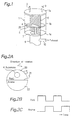
- Fig. 1 shows the construction of a vapor growth apparatus according to a first embodiment of the present invention.
- the vapor growth apparatus has an approximately cylinder-shaped growth chamber 1.
- the growth chamber 1 has a cylindrical portion 1b which extends in a vertical direction, a lid portion 1a which serves as an end plate for closing an upstream end portion of the cylindrical portion 1b, and a bottom portion 1c for closing the downstream end of the cylindrical portion 1b.
- a supply inlet 2 for supplying a cation material gas into the growth chamber 1 and a supply inlet 3 for supplying an anion material gas into the growth chamber 1 are provided in positions symmetrical about the center of the lid portion 1a.
- a cylindrical support pipe 9 which has a diameter smaller than that of the cylindrical portion 1b and supports the growth chamber 1.
- the growth chamber 1 is communicated with the support pipe 9 through an opening provided at the center of the bottom portion 1c, and the support pipe 9 is communicated with an exhaust pipe 10 provided at a peripheral surface thereof.
- Gas existing inside the cylindrical portion 1b of the growth chamber 1 is discharged through the support pipe 9 and the exhaust pipe 10 by a vacuum pump (not shown) which serves as an exhaust means.
- a vacuum pump (not shown) which serves as an exhaust means.
- Inside the support pipe 9 are provided a drive shaft 7 and a drive motor (not shown) which serve as a drive means.
- a disk-shaped substrate holder 5 horizontally, i.e., perpendicular to the center line of the cylindrical portion 1b.
- An upper surface 20 of the substrate holder 5 faces the material gas supply inlets 2 and 3 at the lid portion 1a, and serves as a substrate holding surface on which a substrate 4 is set in a growth stage.
- the center of the substrate holder 5 exists in the center line of the cylindrical portion 1b, and the outer diameter size of the substrate holder 5 is set smaller than the inner diameter size of the cylindrical portion 1b. Consequently, there is achieved a constant gap between the substrate holder 5 and the interior wall of the cylindrical portion 1b with regard to the entire circumference.
- the substrate holder 5 is supported by the drive shaft 7 extending from the drive motor inside the support pipe 9 provided below.
- the axial center of the drive shaft 7 coincides with the center line of the cylindrical portion 1b, and a tip end of the drive shaft 7 is connected to the center of a lower surface of the substrate holder 5.
- the substrate holder 5 is rotated around the center line of the cylindrical portion 1b by the drive motor via the drive shaft 7.
- the substrate holder 5 has therein a built-in heater (not shown) which generates heat by receiving an electricity, thereby allowing the entire area of the substrate holding surface 20 to be uniformly maintained at a specified temperature in the growth stage.
- a partition plate 6 which serves as a gas separation means.
- the partition plate 6 is arranged in a plane which includes the center line of the cylindrical portion 1b and passes between the material gas supply inlets 2 and 3, thereby separating the inside of the cylindrical portion 1b into two areas corresponding to the respective material gas supply inlets 2 and 3.
- the partition plate 6 is put in contact with the interior walls of the lid portion 1a, the cylindrical portion 1b, and the bottom portion 1c.
- the partition plate 6 is formed with a cut portion along the configurations of the members 5 and 7 so that the members 5 and 7 can rotate without friction.
- the partition plate 6 separates the flow paths of the material gases extending from the material gas supply inlets 2 and 3 to the substrate holding surface 20 from each other in the growth stage, thereby forming two material gas supply areas where the material gases are independently supplied to the substrate holding surface 20. Since the partition plate 6 is a mere plate, the flow paths of the material gases can be separated from each other simply and effectively.
- a GaAs layer is to be grown as a compound semiconductor layer on the GaAs substrate 4.
- the substrate 4 is set between the center and the periphery of the substrate holding surface 20 of the substrate holder 5.
- the substrate 4 is maintained at a specified temperature (400 to 550°C) by the built-in heater of the substrate holder 5.
- TMG trimethyl gallium
- arsine which serves as an anion material gas
- the flow rate of TMG is set at 20 SCCM
- the flow rate of arsine is set at 200 SCCM
- the TMG and arsine are each accelerated by hydrogen gas at a flow rate of 5 SLM.
- the gas inside the cylindrical portion 1b is discharged by the vacuum pump through the support pipe 9 and the exhaust pipe 10 provided on the downstream side, whereby a pressure of 20 Torr is achieved inside the growth chamber 1. As a result, a high-speed gas flow is generated inside the cylindrical portion 1b.
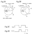
- the TMG and arsine supplied into the cylindrical portion 1b through the material gas supply inlets 2 and 3 are separated from each other by the partition plate 6, and then reach the substrate holding surface 20 of the substrate holder 5 without being mixed with each other. Consequently, as shown in Fig. 2A, two material gas supply areas (a TMG supply area and an arsine supply area) 21 and 22 to which the TMG and arsine are independently supplied are formed on the substrate holding surface 20.
- the substrate holder 5 is rotated around the center line of the cylindrical portion 1b by the drive motor. Therefore, the TMG and arsine are alternately supplied to the surface of the substrate 4 set on the substrate holding surface 20 in a manner as shown in Figs. 2B and 2C.
- a gas supply cycle composed of two periods of a TMG supply period and an arsine supply period is formed.
- the rotating speed of the substrate holder 5 is six turns per minute (constant speed)
- the GaAs substrate 4 is put in contact with each of the TMG and arsine for 5 seconds.
- a GaAs monatomic layer (having a thickness of about 2.8 ⁇ ) was able to be grown on the surface of the substrate 4 every one turn.
- the cation material gas and the anion material gas can be alternately supplied to the surface of the substrate 4 by rotating the substrate holder 5.
- the above-mentioned arrangement obviates the need of frequently opening and closing the control valve for the changeover between the material gas supply periods unlike the conventional case, resulting in eliminating the fear that the durability of the control valve will be impaired.
- control factors in performing the atomic layer growth by means of the present vapor growth apparatus are growth chamber pressure, substrate temperature, gas flow rate, and the rotating speed of the substrate holder, which can be easily controlled.
- a compound semiconductor layer having an evenness and an interfacial sharpness in units of atomic layers can be grown with a good productivity.
- light emitting devices and high-frequency devices having excellent evenness and interfacial sharpness can be produced.
- the GaAs layer can be grown on the substrate 4 with a good controllability.
- TMG trimethyl aluminum
- the rotating speed of the substrate holder 5 is made constant, the present invention is not limited to this. For instance, it is acceptable to increase the rotating speed of the substrate holder 5 when the substrate 4 passes just below the partition plate 6 and reduce the rotating speed or temporarily stop the rotation of the substrate holder 5 when the substrate 4 is located in a position other than the position just below the partition plate 6. With the above-mentioned arrangement, a transitional period in which the TMG is supplied to a part of the surface of the substrate 4 and the arsine is supplied to the remaining part of the surface of the substrate 4 is substantially eliminated. Therefore, growth of an atomic layer having an excellent interfacial sharpness is achieved.
- the rotating speed of the substrate holder 5 may be changed according to the duration of the period in which each of TMG and arsine is supplied to the substrate 4. For instance, the rotating speed at the time when the substrate 4 passes through the arsine supply area 22 is made greater than the rotating speed at the time when the substrate 4 passes through the TMG supply area 21.
- the TMG supply period and the arsine supply period for forming the GaAs layer can be each set at the necessary minimum duration in a manner as shown in Fig. 3C. Therefore, the productivity can be increased.
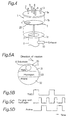
- Fig. 4 shows the construction of a vapor growth apparatus according to a second embodiment of the present invention. It is to be noted that the same components as those shown in Fig. 1 are denoted by the same reference numerals, and no description therefor is provided herein.
- the present vapor growth apparatus uses a separation gas having a characteristic that makes no contribution to the growth reaction on the surface of the substrate 4 instead of the partition plate 6 of the vapor growth apparatus shown in Fig. 1.
- separation gas supply inlets 8, 8, and 8 for supplying a separation gas are provided in a straight line passing between the material gas supply inlets 2 and 3 at the lid portion 1a of the growth chamber 1.
- a layer-like flow of the separation gas extending from the separation gas supply inlets 8, 8, and 8 to the substrate holding surface 20 is formed.
- a GaAs layer is grown as a compound semiconductor layer on the GaAs substrate 4 in the same manner as in the previous embodiment.
- Trimethyl gallium (TMG) is used as a cation material gas
- arsine is used as an anion material gas
- hydrogen is used as a separation gas.
- TMG Trimethyl gallium
- the flow rate of the separation-use hydrogen gas is set at 10 SLM at each inlet.
- the rotating speed of the substrate holder 5 is six turns per minute (constant speed).
- the TMG and arsine supplied into the cylindrical portion 1b through the material gas supply inlets 2 and 3 are separated from each other by the flow of the hydrogen gas in a layer form, and then reach the substrate holding surface 20 of the substrate holder 5 without being mixed with each other. Consequently, as shown in Fig. 5A, a TMG supply area 31 and an arsine supply area 32 are separated from each other by a separation area 33 achieved by the hydrogen gas on the substrate holding surface 20.
- the substrate holder 5 is rotated around the center line of the cylindrical portion 1b shown in Fig. 4. Consequently, as shown in Figs.
- a gas supply cycle composed of four periods of a TMG supply period, a separation period by means of hydrogen, an arsine supply period, and a separation period by means of hydrogen.
- the flow paths of the material gases can be separated from each other without providing any additional member inside the cylindrical portion 1b, which leads to an advantage that the maintenance of the apparatus can be simplified.
- the separation gas is not limited to the hydrogen gas, and the gas is merely required to be a gas having a characteristic that makes no contribution to the growth reaction on the surface of the substrate.
- inactive gas such as argon or helium is used.
- Figs. 8A through 8G show an example in which a GaN layer is grown as a compound semiconductor layer on sapphire substrates 4A and 4B by means of the vapor growth apparatus shown in Fig. 4.
- Trimethyl gallium (TMG) is used as a cation material gas
- ammonia is used as an anion material gas
- hydrogen is used as a separation gas.
- the substrates 4A and 4B are set between the center and the periphery of the substrate holding surface 20 of the substrate holder 5 symmetrically about the center, and the substrate temperature is maintained at 500°C.
- the TMG and ammonia are supplied into the cylindrical portion 1b.
- the flow rate of TMG is set at 20 SCCM, and acceleration is performed by means of the hydrogen gas of a flow rate of 5 SLM.
- the flow rate of ammonia is set at 5 SLM. It is to be noted that the separation gas is not flowed in this point of time.
- the pressure inside the growth chamber 1 is set at 760 Torr by adjusting the displacement of the vacuum pump.
- the rotating speed of the substrate holder 5 is set at about 2000 turns per minute. Since the separation gas is not flowed, the TMG and ammonia are mixed with each other on the two substrates 4A and 4B, thereby growing a GaN buffer layer in the normal MOVPE mode. The reason why the rotating speed of the substrate holder 5 is increased to the high value of 2000 turns per minute is to ensure a uniformity in thickness of the growth layer.
- a GaN atomic layer is grown on the GaN buffer layer.
- the substrate temperature is elevated and maintained within a range of 800 to 1000°C.
- hydrogen gas is flowed through the separation gas supply inlets 8, 8, and 8 at a rate of 10 SLM at each inlet.
- the pressure inside the growth chamber 1 is set at 200 Torr by adjusting the displacement of the vacuum pump. Then the rotating speed of the substrate holder 5 is set at about 10 turns per minute.
- the TMG and ammonia supplied into the cylindrical portion 1b through the material gas supply inlets 2 and 3 are separated from each other by the flow of the hydrogen gas in a layer form, and then reach the substrate holding surface 20 of the substrate holder 5 without being mixed with each other. Consequently, in a manner as shown in Fig. 8A, a TMG supply area 51 and an ammonia supply area 52 are separated from each other by a separation area 53 achieved by the hydrogen gas on the substrate holding surface 20.
- the substrate holder 5 is rotated around the center line of the cylindrical portion 1b shown in Fig. 4. Consequently, in regard to the substrate 4A, as shown in Figs.
- a gas supply cycle composed of four periods of a TMG supply period, a separation period by means of hydrogen, an ammonia supply period, and a separation period by means of hydrogen.
- a gas supply cycle composed of four periods of an ammonia supply period, a separation period by means of hydrogen, a TMG supply period, and a separation period by means of hydrogen in a phase reverse to that of the substrate 4A.
- the gas supply cycles of the substrates 4A and 4B are reverse to each other, there is grown a GaN layer on either one of the substrates 4A and 4B in an atomic layer growth mode. Actually, a GaN monatomic layer (having a thickness of about 2.6 ⁇ ) was able to be grown every one turn.
- the number of substrates is of course not limited to two, and there may be any number of substrates so long as the substrates can be mounted on the substrate holding surface 20.
- Fig. 6 shows the construction of a vapor growth apparatus according to a third embodiment of the present invention. It is to be noted that the same components as those shown in Figs. 1 and 4 are denoted by the same reference numerals, and no description therefor is provided herein.
- the present vapor growth apparatus concurrently uses partition plates 6A and 6B together with a separation gas as a gas separation means.
- separation gas supply inlets 8 and 8 for supplying the separation gas are provided in a straight line passing between the material gas supply inlets 2 and 3 at the lid portion 1a of the growth chamber 1.
- partition plates 6A and 6B are provided inside the cylindrical portion 1b.
- the partition plates 6A and 6B intersect each other in the center line of the cylindrical portion 1b, thereby separating the inside of the cylindrical portion 1b into four areas corresponding to the material gas supply inlets 2 and 3 and the separation gas supply inlets 8 and 8.
- An angle at which the partition plates 6A and 6B intersect each other is set according to the durations of the periods in which the material gases are supplied to the substrate 4.
- the partition plates 6A and 6B separate the flow paths of the material gases and hydrogen gas extending from the material gas supply inlets 2 and 3 and the separation gas supply inlets 8 and 8 to the substrate holding surface 20 in the growth stage. Since the partition plates 6A and 6B and the separation gas are concurrently used, the flow paths of the material gases can be further surely separated from each other.
- a zinc selenide layer is to be grown as a compound semiconductor layer on a GaAs substrate 4.
- Diethyl zinc (DEZ) of one system is used as a cation material gas
- hydrogen selenide of one system is used as an anion material gas
- hydrogen of two systems are used as a separation gas.
- the flow rate of the separation-use hydrogen gas is 5 SLM at each inlet.
- the rotating speed of the substrate holder 5 is ten turns per minute (constant speed).
- the DEZ, hydrogen selenide, and hydrogen of two systems supplied into the cylindrical portion 1b through the material gas supply inlets 2 and 3 and the separation gas supply inlets 8 and 8 are separated from each other by the partition plates 6A and 6B, and then reach the substrate holding surface 20 of the substrate holder 5 without being mixed with each other.
- a DEZ supply area 41, a separation area 42 by means of hydrogen, a hydrogen selenide supply area 43, and a separation area 44 by means of hydrogen are sequentially formed on the substrate holding surface 20 in the circumferential direction.
- the substrate holder 5 is rotated around the center line of the cylindrical portion 1b shown in Fig. 6.
- a gas supply cycle composed of four periods of a DEZ supply period, a separation period by means of hydrogen, a hydrogen selenide supply period, and a separation period by means of hydrogen.
- a zinc selenide monatomic layer (having a thickness of about 2.8 ⁇ ) was able to be grown on the surface of the substrate 4 every one turn.
- the number of partition plates is not limited to two. Three or more partition plates may be provided and made to intersect each other in the center line of the cylindrical portion 1b at specified angles.
- the supply systems of material gases and separation gas can be increased in number by providing a supply system of a material gas or a supply system of a separation gas for every area separated by the partition plates. Therefore, various types of compound semiconductor layers can be grown on the substrate.
- Figs. 9A, 9B, 9C, 9D, and 9E show an example in which a Ga 0.5 In 0.5 P layer is grown as a compound semiconductor layer on a GaAs substrate 4 by means of a vapor growth apparatus of which partition plates are increased in number to three and the other parts of which are similar to those of Fig. 3.
- the vapor growth apparatus used herein concurrently uses partition plates 6A, 6B, and 6C as a gas separation means and two systems of hydrogen as a separation gas in a manner as shown in Fig. 9A.
- the partition plates 6A, 6B, and 6C are intersecting each other at specified angles in the center line of the cylindrical portion 1b shown in Fig. 6.
- the angles at which the partition plates 6A, 6B, and 6C intersect each other are set according to the durations of the periods in which the material gases are supplied to the substrate 4.
- material gases of three types of four systems In detail, one system of TMG and one system of trimethyl indium (TMI) are used as a cation material gas.
- TMI trimethyl indium
- phosphine of two systems as an anion material gas.
- the flow rate of the separation-use hydrogen gas is 3 SLM.
- the rotating speed of the substrate holder 5 is three turns per minute (constant speed).
- the TMG, TMI, phosphine of two systems, and hydrogen of two systems supplied into the cylindrical portion 1b through the material gas supply inlets are separated from each other by the partition plates 6A, 6B, and 6C, and then reach the substrate holding surface 20 of the substrate holder 5 without being mixed with each other.
- a TMG supply area 61, a phosphine supply area 62, a separation area 63 by means of hydrogen, a TMI supply area 64, a phosphine supply area 65, and a separation area 66 by means of hydrogen are sequentially formed in the circumferential direction on the substrate holding surface 20.
- the substrate holder 5 is rotated around the center line of the cylindrical portion 1b shown in Fig. 6. Consequently, there is formed a gas supply cycle composed of six periods of a TMG supply period, a phosphine supply period, a separation period by means of hydrogen, a TMI supply period, a phosphine supply period, and a separation period by means of hydrogen in a manner as shown in Figs. 9B, 9C, 9D and 9E.
- Figs. 10A, 10B, 10C and 10D show an example in which a Ga 0.5 In 0.5 P layer is grown as a compound semiconductor layer on a GaAs substrate 4 by means of the vapor growth apparatus shown in Fig. 6.
- TMG and TMI (referred to as (TMG + TMI)) as a cation material gas to be supplied concurrently to one system, and phosphine of one system is used as an anion material gas.
- hydrogen of two systems as a separation gas.
- the flow rate of the separation-use hydrogen gas is 3 SLM.
- the rotating speed of the substrate holder 5 is three turns per minute (constant speed).
- a (TMG + TMI) supply area 71, a separation area 72 by means of hydrogen, a phosphine supply area 73, and a separation area 74 by means of hydrogen are sequentially formed in the circumferential direction on the substrate holding surface 20.
- the substrate holder 5 is rotated around the center line of the cylindrical portion 1b shown in Fig. 6. Consequently, as shown in Figs. 10B, 10C and 10D, there is formed a gas supply cycle composed of four periods of a (TMG + TMI) supply period, a separation period by means of hydrogen, a phosphine supply period, and a separation period by means of hydrogen.
- a Ga 0.5 In 0.5 p monatomic layer (having a thickness of about 2.8 ⁇ ) was able to be grown on the surface of the substrate 4 every one turn.
- the compound semiconductor layer grown on the substrate has a composition of one type in each of the aforementioned examples
- the compound semiconductor layer may have compositions of a variety of types by changing the type of the material gas in the course of the growth process.
- a material gas containing an impurity element may be used in order to give a conductivity to the compound semiconductor layer to be grown.
- an organic metal compound is used as a cation material gas in each of the aforementioned examples, there may be used a material gas other than the organic metal compound, such as a halogen compound.
- the growth chamber 1 has the cylindrical portion 1b which extends in a vertical direction in each of the vapor growth apparatuses shown in Figs. 1, 4, and 6, the present invention is not limited to this. It is acceptable to arrange the cylindrical portion in a horizontal direction and flow the material gases and separation gas in the horizontal direction.
- the substrate holder 5 may be a high-frequency heating type effected with provision of a coil around the cylindrical portion 1b instead of the built-in heater type.
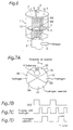
- Fig. 11 shows the construction of a vapor growth apparatus according to a fourth preferred embodiment of the present invention. It is to be noted that the same components as those shown in Fig. 1 are denoted by the same reference numerals, and no description therefor is provided herein.
- an approximately cone frustum-shaped substrate holder 15 having a center line coinciding with the center line of the cylindrical portion 1b is provided at an approximately middle level of the cylindrical portion 1b.
- An exterior side surface 30 of the substrate holder 15 has a pyramidal configuration (pyramidal configuration having a polygonal transverse section) rather than a conical configuration.
- Each segmented small surface between adjacent ridgelines of the exterior side surface 30 has a flatness such that it can allow a substrate 4 to adhere thereto, and serves as a substrate holding surface on which the substrate 4 is set in the growth stage.
- the area of the substrate holding surface 30 can be expanded more than in the case where the substrate holding surface is provided horizontally. Therefore, a lot of substrates 4, 4, ... can be set on the substrate holding surface 30, which resulting in an improved productivity.
- a lower edge of the substrate holder 15 has a circular configuration, and its outer diameter size is set smaller than the inner diameter size of the cylindrical portion 1b.
- the center line of the substrate holder 15 is coinciding with the center line of the cylindrical portion 1b, and consequently a gap between the lower edge and the interior wall of the cylindrical portion 1b is made constant throughout the entire circumference. Therefore, the conductance of exhaust is made constant with regard to the entire circumference of the substrate holder 15. Even when the substrate holder 15 is rotated, no influence is exerted on the flow velocity of each material gas. Therefore, a compound semiconductor layer can be grown on the substrate 4 with a good controllability.
- a partition plate 16 having a cut portion along the configurations of the substrate holder 15 and the drive shaft 7 is provided as a gas separation means inside the cylindrical portion 1b.
- the partition plate 16 is provided in a plane which includes the center line of the cylindrical portion 1b and passes between the material gas supply inlets 2 and 3, thereby separating the inside of the cylindrical portion 1b into two areas corresponding respectively to the material gas supply inlets 2 and 3. Since the flow paths of the material gases are separated from each other by the partition plate 16, a cation material gas and an anion material gas can be alternately supplied to the surface of the substrate 4 by rotating the substrate holder 15. Therefore, a compound semiconductor layer having an evenness and an interfacial sharpness in units of atomic layers can be grown with a good productivity. With the above-mentioned arrangement, light emitting devices and high-frequency devices having excellent evenness and interfacial sharpness can be produced.
- Fig. 12 shows the construction of a vapor growth apparatus according to a fifth preferred embodiment of the present invention. It is to be noted that the same components as those shown in Fig. 1 are denoted by the same reference numerals, and no description therefor is provided herein.
- an approximately cylinder-shaped substrate holder 25 having a center line coinciding with the center line of the cylindrical portion 1b is provided inside the cylindrical portion 1b.
- the substrate holder 25 is supported by the drive shaft 7 which extends from the drive motor inside the support pipe 9 provided below and arm members (not shown) which extends from the circumference of the drive shaft 7 to a lower end of the substrate holder 25.
- An interior surface 40 of the substrate holder 25 has a prismatic configuration (prismatic configuration having a polygonal transverse section) rather than a cylindrical configuration.
- Each segmented small surface between adjacent valleys lines of the interior surface 40 has a flatness such that it can allow a substrate 4 to adhere thereto, and serves as a substrate holding surface on which the substrate 4 is set in the growth stage.
- the area of the substrate holding surface 40 can be expanded more than in the case where the substrate holding surface is provided horizontally, Therefore, a lot of substrates 4, 4, ... can be set on the substrate holding surface 40, which resulting in an improved productivity.
- the substrate holder 25 has an approximately cylinder-shaped configuration. Therefore, even when the substrate holder 25 rotates in the growth stage, no influence is exerted on the speed of flow of each material gas. Therefore, a compound semiconductor layer can be grown on the substrate 4 with a good controllability.
- a partition plate 26 having an approximately T-shaped configuration is provided as a gas separation means inside the cylindrical portion 1b.
- the partition plate 26 is provided in a plane which includes the center line of the cylindrical portion 1b and passes between the material gas supply inlets 2 and 3, thereby separating the inside of the cylindrical portion 1b into two areas corresponding respectively to the material gas supply inlets 2 and 3. Since the flow paths of the material gases are separated from each other by the partition plate 26, a cation material gas and an anion material gas can be alternately supplied to the surface of the substrate 4 by rotating the substrate holder 25. Therefore, a compound semiconductor layer having an evenness and an interfacial sharpness in units of atomic layers can be grown with a good productivity. With the above-mentioned arrangement, light emitting devices and high-frequency devices having excellent evenness and interfacial sharpness can be produced.
- the flow paths of the material gases are separated from each other by the gas separation means in the vapor growth apparatus of the present invention, and therefore the cation material gas and the anion material gas can be alternately supplied to the surface of the substrate by rotating the substrate holder.
- the control valve is not required to be frequently opened and closed for the changeover between the material gas supply periods unlike the conventional case, resulting in eliminating the fear that the durability of the control valve will be impaired.
- a compound semiconductor layer having an evenness and an interfacial sharpness in units of atomic layers can be grown with a good productivity.
- the substrate holding surface of the substrate holder is perpendicular to the center line of the cylindrical portion and has a circular configuration, and the center of the substrate holding surface exists in the center line of the cylindrical portion.
- the gas separation means is comprised of at least one partition plate provided in a plane which includes the center line of the cylindrical portion and passes between the plural number of material gas supply inlets.
- the partition plates extend radially from the center line to the interior wall of the cylindrical portion and intersect each other at a specified angle, and the angle is set according to a duration of a period in which each of the material gases are supplied to the substrate. Therefore, by increasing the setting level of the rotating speed (constant speed) of the substrate holder, each material gas supply period for forming the compound semiconductor layer can be set at the necessary minimum duration. Therefore, the productivity can be increased. Furthermore, since the drive means is merely required to rotate the substrate holder at a constant speed, the rotation control can be performed simply.
- a separation gas supply inlet for supplying the separation gas having a characteristic that makes no contribution to the growth reaction on the surface of the substrate is provided between the plural number of material gas supply inlets at the end plate.
- the gas separation means is comprised of a flow of the separation gas in a layer form extending from the separation gas supply inlet to the substrate holding surface. Therefore, the flow paths of the material gases can be separated from each other without providing any additional member inside the cylindrical portion, thereby allowing a simplified maintenance to be achieved.
- the substrate holding surface of the substrate holder has a configuration corresponding to the exterior side surface of a pyramidal frustum having a center line coinciding with the center line of the cylindrical portion.
- the substrate holding surface of the substrate holder has a configuration corresponding to the interior side surface of a prism-shaped pipe having a center line coinciding with the center line of the cylindrical portion.
- the present invention also provides a vapor growth method comprising the steps of: holding a substrate on a substrate holding surface of a substrate holder arranged between an upstream side and a downstream side of a cylindrical portion of a growth chamber having the cylindrical portion which extends in one direction from the upstream side to the downstream side and an end plate which closes an upstream end portion of the cylindrical portion, maintaining the substrate at a specified temperature; farming material gas supply areas where material gases are independently supplied to corresponding portions of the substrate holding surface by supplying a cation material gas and an anion material gas from the upstream side through a plurality of material gas supply inlets into the cylindrical portion while preventing the material gases from being mixed with each other inside the cylindrical portion by gas separation means and discharging the material gases out of the cylindrical portion, and rotating the substrate holder around a center line of the cylindrical portion.
- the cation material gas and the anion material gas can be alternately supplied to the surface of the substrate by rotating the substrate holder while preventing the material gases from being mixed by the separation means, and a compound semiconductor layer having an evenness and an interfacial sharpness in units of atomic layers can be grown with a good productivity. Furthermore, the above-mentioned arrangement obviates the need of frequently opening and closing the control valve.
- the rotating speed of the substrate holder is increased when the substrate traverses the plane in which the partition plate exists, and the rotating speed of the substrate holder is reduced or temporarily stopped when the substrate is located in each material gas supply area.
- the rotating speed of the substrate holder rotating around the center line of the cylindrical portion is changed according to the duration of the period in which each material gas is supplied to the substrate. For instance, when the substrate passes through the supply area of the material gas which requires a short supply time, the rotating speed of the substrate holder is increased. When the substrate passes through the supply area of the material gas which requires a long supply time, the rotating speed of the substrate holder is reduced. With the above-mentioned arrangement, each material gas supply period for forming the compound semiconductor layer can be set at the necessary minimum duration. Therefore, the productivity can be increased.
- the vapor growth method of an embodiment there are prepared two or more types of at least one of the cation material gas and the anion material gas, and the two or more types of material gases are supplied into the cylindrical portion through different material gas supply inlets, whereby two or more atomic layers are grown in one turn of the substrate holder. Therefore, a compound semiconductor layer having a composition of a variety of types can be grown.
- SCCM and SLM represent units of flow rate.
- S is an abbreviation for the standard condition in which the temperature is 0 C and the pressure is 1 atm, and means that the volume of gas under a certain condition is converted into the volume of the gas under the standard condition.
- CC is an abbreviation for cubic centimeter.
- L is an abbreviation for liter, and “M” means “per minute”. Therefore, for example “1SCCM” means that the gas of 1 cc if converted to the standard condition flows per minute.
- 1SLM means that the gas of 1 liter if converted to the standard condition flow per minute.
Landscapes
- Chemical & Material Sciences (AREA)
- Engineering & Computer Science (AREA)
- Materials Engineering (AREA)
- Metallurgy (AREA)
- Organic Chemistry (AREA)
- General Chemical & Material Sciences (AREA)
- Chemical Kinetics & Catalysis (AREA)
- Mechanical Engineering (AREA)
- Crystallography & Structural Chemistry (AREA)
- Inorganic Chemistry (AREA)
- Crystals, And After-Treatments Of Crystals (AREA)
- Chemical Vapour Deposition (AREA)
Applications Claiming Priority (3)
| Application Number | Priority Date | Filing Date | Title |
|---|---|---|---|
| JP10676094 | 1994-05-20 | ||
| JP10676094A JP3181171B2 (ja) | 1994-05-20 | 1994-05-20 | 気相成長装置および気相成長方法 |
| EP95303333A EP0683249B1 (de) | 1994-05-20 | 1995-05-18 | Verfahren zur Züchtung einer Halbleiterverbindungsschicht |
Related Parent Applications (1)
| Application Number | Title | Priority Date | Filing Date |
|---|---|---|---|
| EP95303333A Division EP0683249B1 (de) | 1994-05-20 | 1995-05-18 | Verfahren zur Züchtung einer Halbleiterverbindungsschicht |
Publications (3)
| Publication Number | Publication Date |
|---|---|
| EP0964083A2 true EP0964083A2 (de) | 1999-12-15 |
| EP0964083A3 EP0964083A3 (de) | 2002-01-30 |
| EP0964083B1 EP0964083B1 (de) | 2004-07-14 |
Family
ID=14441872
Family Applications (2)
| Application Number | Title | Priority Date | Filing Date |
|---|---|---|---|
| EP99202642A Expired - Lifetime EP0964083B1 (de) | 1994-05-20 | 1995-05-18 | Vorrichtung zur Züchtung einer Verbindungshalbleiterschicht |
| EP95303333A Expired - Lifetime EP0683249B1 (de) | 1994-05-20 | 1995-05-18 | Verfahren zur Züchtung einer Halbleiterverbindungsschicht |
Family Applications After (1)
| Application Number | Title | Priority Date | Filing Date |
|---|---|---|---|
| EP95303333A Expired - Lifetime EP0683249B1 (de) | 1994-05-20 | 1995-05-18 | Verfahren zur Züchtung einer Halbleiterverbindungsschicht |
Country Status (7)
| Country | Link |
|---|---|
| US (1) | US5730802A (de) |
| EP (2) | EP0964083B1 (de) |
| JP (1) | JP3181171B2 (de) |
| KR (1) | KR0173013B1 (de) |
| CN (1) | CN1060233C (de) |
| DE (2) | DE69533268T2 (de) |
| TW (1) | TW265458B (de) |
Cited By (1)
| Publication number | Priority date | Publication date | Assignee | Title |
|---|---|---|---|---|
| NL1014734C2 (nl) * | 2000-03-23 | 2001-09-25 | Huga Optotech Inc | Werkwijze voor het vormen van groep III-nitride toplagen door epitaxiale groei op een monokristalsubstraat door gebruikmaking van afwisselende toevoegingen van reactanten (EGAS), producten die daarvan gemaakt zijn en een inrichting daarvoor. |
Families Citing this family (452)
| Publication number | Priority date | Publication date | Assignee | Title |
|---|---|---|---|---|
| WO1997036320A1 (en) * | 1996-03-22 | 1997-10-02 | Nippon Sanso Corporation | Vapor phase growth apparatus and vapor phase growth method |
| US6342277B1 (en) * | 1996-08-16 | 2002-01-29 | Licensee For Microelectronics: Asm America, Inc. | Sequential chemical vapor deposition |
| US5807792A (en) * | 1996-12-18 | 1998-09-15 | Siemens Aktiengesellschaft | Uniform distribution of reactants in a device layer |
| US6671223B2 (en) * | 1996-12-20 | 2003-12-30 | Westerngeco, L.L.C. | Control devices for controlling the position of a marine seismic streamer |
| US5888886A (en) * | 1997-06-30 | 1999-03-30 | Sdl, Inc. | Method of doping gan layers p-type for device fabrication |
| KR100712241B1 (ko) * | 1999-05-13 | 2007-04-27 | 이엠에프 아일랜드 리미티드 | 기판상에 재료를 에피택셜성장시키는 방법 및 장치 |
| US6620723B1 (en) | 2000-06-27 | 2003-09-16 | Applied Materials, Inc. | Formation of boride barrier layers using chemisorption techniques |
| US6551929B1 (en) | 2000-06-28 | 2003-04-22 | Applied Materials, Inc. | Bifurcated deposition process for depositing refractory metal layers employing atomic layer deposition and chemical vapor deposition techniques |
| US7405158B2 (en) * | 2000-06-28 | 2008-07-29 | Applied Materials, Inc. | Methods for depositing tungsten layers employing atomic layer deposition techniques |
| US7964505B2 (en) * | 2005-01-19 | 2011-06-21 | Applied Materials, Inc. | Atomic layer deposition of tungsten materials |
| US7732327B2 (en) | 2000-06-28 | 2010-06-08 | Applied Materials, Inc. | Vapor deposition of tungsten materials |
| US7101795B1 (en) * | 2000-06-28 | 2006-09-05 | Applied Materials, Inc. | Method and apparatus for depositing refractory metal layers employing sequential deposition techniques to form a nucleation layer |
| KR100458982B1 (ko) * | 2000-08-09 | 2004-12-03 | 주성엔지니어링(주) | 회전형 가스분사기를 가지는 반도체소자 제조장치 및 이를이용한 박막증착방법 |
| JP4511006B2 (ja) * | 2000-09-01 | 2010-07-28 | 独立行政法人理化学研究所 | 半導体の不純物ドーピング方法 |
| US6825447B2 (en) * | 2000-12-29 | 2004-11-30 | Applied Materials, Inc. | Apparatus and method for uniform substrate heating and contaminate collection |
| US6998579B2 (en) | 2000-12-29 | 2006-02-14 | Applied Materials, Inc. | Chamber for uniform substrate heating |
| US20020083897A1 (en) * | 2000-12-29 | 2002-07-04 | Applied Materials, Inc. | Full glass substrate deposition in plasma enhanced chemical vapor deposition |
| US6765178B2 (en) | 2000-12-29 | 2004-07-20 | Applied Materials, Inc. | Chamber for uniform substrate heating |
| US20020127336A1 (en) * | 2001-01-16 | 2002-09-12 | Applied Materials, Inc. | Method for growing thin films by catalytic enhancement |
| US6811814B2 (en) | 2001-01-16 | 2004-11-02 | Applied Materials, Inc. | Method for growing thin films by catalytic enhancement |
| US6951804B2 (en) * | 2001-02-02 | 2005-10-04 | Applied Materials, Inc. | Formation of a tantalum-nitride layer |
| US6878206B2 (en) * | 2001-07-16 | 2005-04-12 | Applied Materials, Inc. | Lid assembly for a processing system to facilitate sequential deposition techniques |
| US6660126B2 (en) | 2001-03-02 | 2003-12-09 | Applied Materials, Inc. | Lid assembly for a processing system to facilitate sequential deposition techniques |
| US6734020B2 (en) | 2001-03-07 | 2004-05-11 | Applied Materials, Inc. | Valve control system for atomic layer deposition chamber |
| US6849545B2 (en) | 2001-06-20 | 2005-02-01 | Applied Materials, Inc. | System and method to form a composite film stack utilizing sequential deposition techniques |
| US20070009658A1 (en) * | 2001-07-13 | 2007-01-11 | Yoo Jong H | Pulse nucleation enhanced nucleation technique for improved step coverage and better gap fill for WCVD process |
| US7211144B2 (en) * | 2001-07-13 | 2007-05-01 | Applied Materials, Inc. | Pulsed nucleation deposition of tungsten layers |
| US20030029715A1 (en) * | 2001-07-25 | 2003-02-13 | Applied Materials, Inc. | An Apparatus For Annealing Substrates In Physical Vapor Deposition Systems |
| US8110489B2 (en) * | 2001-07-25 | 2012-02-07 | Applied Materials, Inc. | Process for forming cobalt-containing materials |
| JP2005504885A (ja) * | 2001-07-25 | 2005-02-17 | アプライド マテリアルズ インコーポレイテッド | 新規なスパッタ堆積方法を使用したバリア形成 |
| US20090004850A1 (en) | 2001-07-25 | 2009-01-01 | Seshadri Ganguli | Process for forming cobalt and cobalt silicide materials in tungsten contact applications |
| US9051641B2 (en) * | 2001-07-25 | 2015-06-09 | Applied Materials, Inc. | Cobalt deposition on barrier surfaces |
| US20080268635A1 (en) * | 2001-07-25 | 2008-10-30 | Sang-Ho Yu | Process for forming cobalt and cobalt silicide materials in copper contact applications |
| US7085616B2 (en) | 2001-07-27 | 2006-08-01 | Applied Materials, Inc. | Atomic layer deposition apparatus |
| DE10141084A1 (de) * | 2001-08-22 | 2002-11-28 | Infineon Technologies Ag | Vorrichtung zur Abscheidung von dünnen Schichten auf einem Stubstrat und entsprechendes Verfahren |
| US6718126B2 (en) * | 2001-09-14 | 2004-04-06 | Applied Materials, Inc. | Apparatus and method for vaporizing solid precursor for CVD or atomic layer deposition |
| US20030059538A1 (en) * | 2001-09-26 | 2003-03-27 | Applied Materials, Inc. | Integration of barrier layer and seed layer |
| US7049226B2 (en) | 2001-09-26 | 2006-05-23 | Applied Materials, Inc. | Integration of ALD tantalum nitride for copper metallization |
| US6936906B2 (en) | 2001-09-26 | 2005-08-30 | Applied Materials, Inc. | Integration of barrier layer and seed layer |
| US6916398B2 (en) | 2001-10-26 | 2005-07-12 | Applied Materials, Inc. | Gas delivery apparatus and method for atomic layer deposition |
| US7780785B2 (en) | 2001-10-26 | 2010-08-24 | Applied Materials, Inc. | Gas delivery apparatus for atomic layer deposition |
| US7204886B2 (en) * | 2002-11-14 | 2007-04-17 | Applied Materials, Inc. | Apparatus and method for hybrid chemical processing |
| KR100782529B1 (ko) * | 2001-11-08 | 2007-12-06 | 에이에스엠지니텍코리아 주식회사 | 증착 장치 |
| US6729824B2 (en) | 2001-12-14 | 2004-05-04 | Applied Materials, Inc. | Dual robot processing system |
| WO2003062490A2 (en) * | 2002-01-17 | 2003-07-31 | Sundew Technologies, Llc | Ald apparatus and method |
| WO2003065424A2 (en) * | 2002-01-25 | 2003-08-07 | Applied Materials, Inc. | Apparatus for cyclical deposition of thin films |
| US6911391B2 (en) * | 2002-01-26 | 2005-06-28 | Applied Materials, Inc. | Integration of titanium and titanium nitride layers |
| US6866746B2 (en) * | 2002-01-26 | 2005-03-15 | Applied Materials, Inc. | Clamshell and small volume chamber with fixed substrate support |
| US6998014B2 (en) | 2002-01-26 | 2006-02-14 | Applied Materials, Inc. | Apparatus and method for plasma assisted deposition |
| US6827978B2 (en) * | 2002-02-11 | 2004-12-07 | Applied Materials, Inc. | Deposition of tungsten films |
| US6833161B2 (en) * | 2002-02-26 | 2004-12-21 | Applied Materials, Inc. | Cyclical deposition of tungsten nitride for metal oxide gate electrode |
| US6972267B2 (en) * | 2002-03-04 | 2005-12-06 | Applied Materials, Inc. | Sequential deposition of tantalum nitride using a tantalum-containing precursor and a nitrogen-containing precursor |
| US6800134B2 (en) | 2002-03-26 | 2004-10-05 | Micron Technology, Inc. | Chemical vapor deposition methods and atomic layer deposition methods |
| US7439191B2 (en) * | 2002-04-05 | 2008-10-21 | Applied Materials, Inc. | Deposition of silicon layers for active matrix liquid crystal display (AMLCD) applications |
| US6846516B2 (en) * | 2002-04-08 | 2005-01-25 | Applied Materials, Inc. | Multiple precursor cyclical deposition system |
| US6720027B2 (en) | 2002-04-08 | 2004-04-13 | Applied Materials, Inc. | Cyclical deposition of a variable content titanium silicon nitride layer |
| US6869838B2 (en) * | 2002-04-09 | 2005-03-22 | Applied Materials, Inc. | Deposition of passivation layers for active matrix liquid crystal display (AMLCD) applications |
| US6875271B2 (en) | 2002-04-09 | 2005-04-05 | Applied Materials, Inc. | Simultaneous cyclical deposition in different processing regions |
| US20030194825A1 (en) * | 2002-04-10 | 2003-10-16 | Kam Law | Deposition of gate metallization for active matrix liquid crystal display (AMLCD) applications |
| US7279432B2 (en) | 2002-04-16 | 2007-10-09 | Applied Materials, Inc. | System and method for forming an integrated barrier layer |
| JP4158139B2 (ja) * | 2002-04-30 | 2008-10-01 | スズキ株式会社 | 薄膜の製造方法およびその装置 |
| US7186385B2 (en) * | 2002-07-17 | 2007-03-06 | Applied Materials, Inc. | Apparatus for providing gas to a processing chamber |
| US6915592B2 (en) * | 2002-07-29 | 2005-07-12 | Applied Materials, Inc. | Method and apparatus for generating gas to a processing chamber |
| KR100483208B1 (ko) * | 2002-08-02 | 2005-04-15 | 주성엔지니어링(주) | 원자층증착방법용 박막증착장치의 밸브 시스템 |
| US6821563B2 (en) | 2002-10-02 | 2004-11-23 | Applied Materials, Inc. | Gas distribution system for cyclical layer deposition |
| US20040065255A1 (en) * | 2002-10-02 | 2004-04-08 | Applied Materials, Inc. | Cyclical layer deposition system |
| US20040069227A1 (en) * | 2002-10-09 | 2004-04-15 | Applied Materials, Inc. | Processing chamber configured for uniform gas flow |
| US6905737B2 (en) * | 2002-10-11 | 2005-06-14 | Applied Materials, Inc. | Method of delivering activated species for rapid cyclical deposition |
| US7262133B2 (en) | 2003-01-07 | 2007-08-28 | Applied Materials, Inc. | Enhancement of copper line reliability using thin ALD tan film to cap the copper line |
| JP4528489B2 (ja) * | 2003-01-27 | 2010-08-18 | 独立行政法人理化学研究所 | p型半導体を用いた紫外発光素子 |
| US20040177813A1 (en) | 2003-03-12 | 2004-09-16 | Applied Materials, Inc. | Substrate support lift mechanism |
| US7342984B1 (en) | 2003-04-03 | 2008-03-11 | Zilog, Inc. | Counting clock cycles over the duration of a first character and using a remainder value to determine when to sample a bit of a second character |
| US20040198069A1 (en) | 2003-04-04 | 2004-10-07 | Applied Materials, Inc. | Method for hafnium nitride deposition |
| WO2004113585A2 (en) * | 2003-06-18 | 2004-12-29 | Applied Materials, Inc. | Atomic layer deposition of barrier materials |
| US20050095859A1 (en) * | 2003-11-03 | 2005-05-05 | Applied Materials, Inc. | Precursor delivery system with rate control |
| US20050252449A1 (en) | 2004-05-12 | 2005-11-17 | Nguyen Son T | Control of gas flow and delivery to suppress the formation of particles in an MOCVD/ALD system |
| US20060019033A1 (en) * | 2004-05-21 | 2006-01-26 | Applied Materials, Inc. | Plasma treatment of hafnium-containing materials |
| US8119210B2 (en) * | 2004-05-21 | 2012-02-21 | Applied Materials, Inc. | Formation of a silicon oxynitride layer on a high-k dielectric material |
| US8323754B2 (en) * | 2004-05-21 | 2012-12-04 | Applied Materials, Inc. | Stabilization of high-k dielectric materials |
| US20060153995A1 (en) * | 2004-05-21 | 2006-07-13 | Applied Materials, Inc. | Method for fabricating a dielectric stack |
| JP4502198B2 (ja) * | 2004-10-21 | 2010-07-14 | ルネサスエレクトロニクス株式会社 | エッチング装置およびエッチング方法 |
| US8159428B2 (en) * | 2005-02-23 | 2012-04-17 | Pixtronix, Inc. | Display methods and apparatus |
| US20070049043A1 (en) * | 2005-08-23 | 2007-03-01 | Applied Materials, Inc. | Nitrogen profile engineering in HI-K nitridation for device performance enhancement and reliability improvement |
| US7402534B2 (en) * | 2005-08-26 | 2008-07-22 | Applied Materials, Inc. | Pretreatment processes within a batch ALD reactor |
| US20070065578A1 (en) * | 2005-09-21 | 2007-03-22 | Applied Materials, Inc. | Treatment processes for a batch ALD reactor |
| US7464917B2 (en) * | 2005-10-07 | 2008-12-16 | Appiled Materials, Inc. | Ampoule splash guard apparatus |
| US20070119371A1 (en) * | 2005-11-04 | 2007-05-31 | Paul Ma | Apparatus and process for plasma-enhanced atomic layer deposition |
| DE102005055468A1 (de) * | 2005-11-22 | 2007-05-24 | Aixtron Ag | Verfahren zum Abscheiden von Schichten in einem CVD-Reaktor sowie Gaseinlassorgan für einen CVD-Reaktor |
| US20070218702A1 (en) * | 2006-03-15 | 2007-09-20 | Asm Japan K.K. | Semiconductor-processing apparatus with rotating susceptor |
| US20070215036A1 (en) * | 2006-03-15 | 2007-09-20 | Hyung-Sang Park | Method and apparatus of time and space co-divided atomic layer deposition |
| US7798096B2 (en) | 2006-05-05 | 2010-09-21 | Applied Materials, Inc. | Plasma, UV and ion/neutral assisted ALD or CVD in a batch tool |
| US8187679B2 (en) * | 2006-07-29 | 2012-05-29 | Lotus Applied Technology, Llc | Radical-enhanced atomic layer deposition system and method |
| US7601648B2 (en) | 2006-07-31 | 2009-10-13 | Applied Materials, Inc. | Method for fabricating an integrated gate dielectric layer for field effect transistors |
| KR20080027009A (ko) * | 2006-09-22 | 2008-03-26 | 에이에스엠지니텍코리아 주식회사 | 원자층 증착 장치 및 그를 이용한 다층막 증착 방법 |
| US7775508B2 (en) * | 2006-10-31 | 2010-08-17 | Applied Materials, Inc. | Ampoule for liquid draw and vapor draw with a continuous level sensor |
| US7799377B2 (en) * | 2006-12-07 | 2010-09-21 | Electronics And Telecommunications Research Institute | Organic/inorganic thin film deposition method |
| US20080206987A1 (en) * | 2007-01-29 | 2008-08-28 | Gelatos Avgerinos V | Process for tungsten nitride deposition by a temperature controlled lid assembly |
| US8043432B2 (en) * | 2007-02-12 | 2011-10-25 | Tokyo Electron Limited | Atomic layer deposition systems and methods |
| WO2008117750A1 (ja) * | 2007-03-23 | 2008-10-02 | Tokuyama Corporation | P型iii族窒化物半導体およびiii族窒化物半導体素子 |
| US20080241384A1 (en) * | 2007-04-02 | 2008-10-02 | Asm Genitech Korea Ltd. | Lateral flow deposition apparatus and method of depositing film by using the apparatus |
| KR100905278B1 (ko) * | 2007-07-19 | 2009-06-29 | 주식회사 아이피에스 | 박막증착장치, 박막증착방법 및 반도체 소자의 갭-필 방법 |
| US20090035946A1 (en) * | 2007-07-31 | 2009-02-05 | Asm International N.V. | In situ deposition of different metal-containing films using cyclopentadienyl metal precursors |
| EP2042619A3 (de) * | 2007-09-28 | 2010-06-02 | OSRAM Opto Semiconductors GmbH | Beschichtungsvorrichtung und Verfahren zu deren Betrieb |
| DE102008010041A1 (de) * | 2007-09-28 | 2009-04-02 | Osram Opto Semiconductors Gmbh | Schichtabscheidevorrichtung und Verfahren zu deren Betrieb |
| KR101376336B1 (ko) * | 2007-11-27 | 2014-03-18 | 한국에이에스엠지니텍 주식회사 | 원자층 증착 장치 |
| US8273178B2 (en) * | 2008-02-28 | 2012-09-25 | Asm Genitech Korea Ltd. | Thin film deposition apparatus and method of maintaining the same |
| US8383525B2 (en) * | 2008-04-25 | 2013-02-26 | Asm America, Inc. | Plasma-enhanced deposition process for forming a metal oxide thin film and related structures |
| KR101436564B1 (ko) * | 2008-05-07 | 2014-09-02 | 한국에이에스엠지니텍 주식회사 | 비정질 실리콘 박막 형성 방법 |
| JP5195676B2 (ja) * | 2008-08-29 | 2013-05-08 | 東京エレクトロン株式会社 | 成膜装置、基板処理装置、成膜方法及び記憶媒体 |
| JP5253932B2 (ja) | 2008-09-04 | 2013-07-31 | 東京エレクトロン株式会社 | 成膜装置、基板処理装置、成膜方法及び記憶媒体 |
| US8146896B2 (en) * | 2008-10-31 | 2012-04-03 | Applied Materials, Inc. | Chemical precursor ampoule for vapor deposition processes |
| US9394608B2 (en) | 2009-04-06 | 2016-07-19 | Asm America, Inc. | Semiconductor processing reactor and components thereof |
| JP5500876B2 (ja) | 2009-06-08 | 2014-05-21 | キヤノン株式会社 | 光電変換装置の製造方法 |
| US8802201B2 (en) | 2009-08-14 | 2014-08-12 | Asm America, Inc. | Systems and methods for thin-film deposition of metal oxides using excited nitrogen-oxygen species |
| JP5310512B2 (ja) * | 2009-12-02 | 2013-10-09 | 東京エレクトロン株式会社 | 基板処理装置 |
| JP5392069B2 (ja) * | 2009-12-25 | 2014-01-22 | 東京エレクトロン株式会社 | 成膜装置 |
| US8637123B2 (en) * | 2009-12-29 | 2014-01-28 | Lotus Applied Technology, Llc | Oxygen radical generation for radical-enhanced thin film deposition |
| US8133806B1 (en) | 2010-09-30 | 2012-03-13 | S.O.I.Tec Silicon On Insulator Technologies | Systems and methods for forming semiconductor materials by atomic layer deposition |
| JP5369304B2 (ja) * | 2010-09-30 | 2013-12-18 | ソイテック | 原子層堆積によって半導体材料を形成するためのシステム及び方法 |
| US8143147B1 (en) * | 2011-02-10 | 2012-03-27 | Intermolecular, Inc. | Methods and systems for forming thin films |
| US9312155B2 (en) | 2011-06-06 | 2016-04-12 | Asm Japan K.K. | High-throughput semiconductor-processing apparatus equipped with multiple dual-chamber modules |
| US10854498B2 (en) | 2011-07-15 | 2020-12-01 | Asm Ip Holding B.V. | Wafer-supporting device and method for producing same |
| US20130023129A1 (en) | 2011-07-20 | 2013-01-24 | Asm America, Inc. | Pressure transmitter for a semiconductor processing environment |
| US9017481B1 (en) | 2011-10-28 | 2015-04-28 | Asm America, Inc. | Process feed management for semiconductor substrate processing |
| KR102152786B1 (ko) | 2012-07-13 | 2020-09-08 | 갈리움 엔터프라이지즈 피티와이 엘티디 | 필름 형성 장치 및 방법 |
| US10714315B2 (en) | 2012-10-12 | 2020-07-14 | Asm Ip Holdings B.V. | Semiconductor reaction chamber showerhead |
| CN103074674B (zh) * | 2013-01-10 | 2015-05-13 | 中国科学院半导体研究所 | 用于金属有机化学气相沉积设备的反应室进气装置 |
| US20160376700A1 (en) | 2013-02-01 | 2016-12-29 | Asm Ip Holding B.V. | System for treatment of deposition reactor |
| US10683571B2 (en) | 2014-02-25 | 2020-06-16 | Asm Ip Holding B.V. | Gas supply manifold and method of supplying gases to chamber using same |
| US10167557B2 (en) | 2014-03-18 | 2019-01-01 | Asm Ip Holding B.V. | Gas distribution system, reactor including the system, and methods of using the same |
| US11015245B2 (en) | 2014-03-19 | 2021-05-25 | Asm Ip Holding B.V. | Gas-phase reactor and system having exhaust plenum and components thereof |
| US10858737B2 (en) | 2014-07-28 | 2020-12-08 | Asm Ip Holding B.V. | Showerhead assembly and components thereof |
| US9890456B2 (en) | 2014-08-21 | 2018-02-13 | Asm Ip Holding B.V. | Method and system for in situ formation of gas-phase compounds |
| US9657845B2 (en) | 2014-10-07 | 2017-05-23 | Asm Ip Holding B.V. | Variable conductance gas distribution apparatus and method |
| US10941490B2 (en) | 2014-10-07 | 2021-03-09 | Asm Ip Holding B.V. | Multiple temperature range susceptor, assembly, reactor and system including the susceptor, and methods of using the same |
| US10276355B2 (en) | 2015-03-12 | 2019-04-30 | Asm Ip Holding B.V. | Multi-zone reactor, system including the reactor, and method of using the same |
| US10458018B2 (en) | 2015-06-26 | 2019-10-29 | Asm Ip Holding B.V. | Structures including metal carbide material, devices including the structures, and methods of forming same |
| US10600673B2 (en) | 2015-07-07 | 2020-03-24 | Asm Ip Holding B.V. | Magnetic susceptor to baseplate seal |
| US10781533B2 (en) * | 2015-07-31 | 2020-09-22 | Applied Materials, Inc. | Batch processing chamber |
| US10211308B2 (en) | 2015-10-21 | 2019-02-19 | Asm Ip Holding B.V. | NbMC layers |
| US11139308B2 (en) | 2015-12-29 | 2021-10-05 | Asm Ip Holding B.V. | Atomic layer deposition of III-V compounds to form V-NAND devices |
| US10529554B2 (en) | 2016-02-19 | 2020-01-07 | Asm Ip Holding B.V. | Method for forming silicon nitride film selectively on sidewalls or flat surfaces of trenches |
| US10343920B2 (en) | 2016-03-18 | 2019-07-09 | Asm Ip Holding B.V. | Aligned carbon nanotubes |
| US10190213B2 (en) | 2016-04-21 | 2019-01-29 | Asm Ip Holding B.V. | Deposition of metal borides |
| US10865475B2 (en) | 2016-04-21 | 2020-12-15 | Asm Ip Holding B.V. | Deposition of metal borides and silicides |
| US10032628B2 (en) | 2016-05-02 | 2018-07-24 | Asm Ip Holding B.V. | Source/drain performance through conformal solid state doping |
| US10367080B2 (en) | 2016-05-02 | 2019-07-30 | Asm Ip Holding B.V. | Method of forming a germanium oxynitride film |
| US11453943B2 (en) | 2016-05-25 | 2022-09-27 | Asm Ip Holding B.V. | Method for forming carbon-containing silicon/metal oxide or nitride film by ALD using silicon precursor and hydrocarbon precursor |
| US10612137B2 (en) | 2016-07-08 | 2020-04-07 | Asm Ip Holdings B.V. | Organic reactants for atomic layer deposition |
| US9859151B1 (en) | 2016-07-08 | 2018-01-02 | Asm Ip Holding B.V. | Selective film deposition method to form air gaps |
| US10714385B2 (en) | 2016-07-19 | 2020-07-14 | Asm Ip Holding B.V. | Selective deposition of tungsten |
| US9887082B1 (en) | 2016-07-28 | 2018-02-06 | Asm Ip Holding B.V. | Method and apparatus for filling a gap |
| KR102532607B1 (ko) | 2016-07-28 | 2023-05-15 | 에이에스엠 아이피 홀딩 비.브이. | 기판 가공 장치 및 그 동작 방법 |
| US9812320B1 (en) | 2016-07-28 | 2017-11-07 | Asm Ip Holding B.V. | Method and apparatus for filling a gap |
| US10643826B2 (en) | 2016-10-26 | 2020-05-05 | Asm Ip Holdings B.V. | Methods for thermally calibrating reaction chambers |
| US11532757B2 (en) | 2016-10-27 | 2022-12-20 | Asm Ip Holding B.V. | Deposition of charge trapping layers |
| US10714350B2 (en) | 2016-11-01 | 2020-07-14 | ASM IP Holdings, B.V. | Methods for forming a transition metal niobium nitride film on a substrate by atomic layer deposition and related semiconductor device structures |
| US10229833B2 (en) | 2016-11-01 | 2019-03-12 | Asm Ip Holding B.V. | Methods for forming a transition metal nitride film on a substrate by atomic layer deposition and related semiconductor device structures |
| US10643904B2 (en) | 2016-11-01 | 2020-05-05 | Asm Ip Holdings B.V. | Methods for forming a semiconductor device and related semiconductor device structures |
| US10134757B2 (en) | 2016-11-07 | 2018-11-20 | Asm Ip Holding B.V. | Method of processing a substrate and a device manufactured by using the method |
| KR102546317B1 (ko) | 2016-11-15 | 2023-06-21 | 에이에스엠 아이피 홀딩 비.브이. | 기체 공급 유닛 및 이를 포함하는 기판 처리 장치 |
| KR102762543B1 (ko) | 2016-12-14 | 2025-02-05 | 에이에스엠 아이피 홀딩 비.브이. | 기판 처리 장치 |
| US11447861B2 (en) | 2016-12-15 | 2022-09-20 | Asm Ip Holding B.V. | Sequential infiltration synthesis apparatus and a method of forming a patterned structure |
| US11581186B2 (en) * | 2016-12-15 | 2023-02-14 | Asm Ip Holding B.V. | Sequential infiltration synthesis apparatus |
| KR102700194B1 (ko) | 2016-12-19 | 2024-08-28 | 에이에스엠 아이피 홀딩 비.브이. | 기판 처리 장치 |
| US10269558B2 (en) | 2016-12-22 | 2019-04-23 | Asm Ip Holding B.V. | Method of forming a structure on a substrate |
| US10867788B2 (en) | 2016-12-28 | 2020-12-15 | Asm Ip Holding B.V. | Method of forming a structure on a substrate |
| US11390950B2 (en) | 2017-01-10 | 2022-07-19 | Asm Ip Holding B.V. | Reactor system and method to reduce residue buildup during a film deposition process |
| US10655221B2 (en) | 2017-02-09 | 2020-05-19 | Asm Ip Holding B.V. | Method for depositing oxide film by thermal ALD and PEALD |
| US10468261B2 (en) | 2017-02-15 | 2019-11-05 | Asm Ip Holding B.V. | Methods for forming a metallic film on a substrate by cyclical deposition and related semiconductor device structures |
| US10529563B2 (en) | 2017-03-29 | 2020-01-07 | Asm Ip Holdings B.V. | Method for forming doped metal oxide films on a substrate by cyclical deposition and related semiconductor device structures |
| USD876504S1 (en) | 2017-04-03 | 2020-02-25 | Asm Ip Holding B.V. | Exhaust flow control ring for semiconductor deposition apparatus |
| KR102457289B1 (ko) | 2017-04-25 | 2022-10-21 | 에이에스엠 아이피 홀딩 비.브이. | 박막 증착 방법 및 반도체 장치의 제조 방법 |
| US10770286B2 (en) | 2017-05-08 | 2020-09-08 | Asm Ip Holdings B.V. | Methods for selectively forming a silicon nitride film on a substrate and related semiconductor device structures |
| US10892156B2 (en) | 2017-05-08 | 2021-01-12 | Asm Ip Holding B.V. | Methods for forming a silicon nitride film on a substrate and related semiconductor device structures |
| US12040200B2 (en) | 2017-06-20 | 2024-07-16 | Asm Ip Holding B.V. | Semiconductor processing apparatus and methods for calibrating a semiconductor processing apparatus |
| US11306395B2 (en) | 2017-06-28 | 2022-04-19 | Asm Ip Holding B.V. | Methods for depositing a transition metal nitride film on a substrate by atomic layer deposition and related deposition apparatus |
| TWI619840B (zh) * | 2017-06-30 | 2018-04-01 | 國立交通大學 | 化學氣相沈積裝置 |
| US10685834B2 (en) | 2017-07-05 | 2020-06-16 | Asm Ip Holdings B.V. | Methods for forming a silicon germanium tin layer and related semiconductor device structures |
| KR20190009245A (ko) | 2017-07-18 | 2019-01-28 | 에이에스엠 아이피 홀딩 비.브이. | 반도체 소자 구조물 형성 방법 및 관련된 반도체 소자 구조물 |
| US10541333B2 (en) | 2017-07-19 | 2020-01-21 | Asm Ip Holding B.V. | Method for depositing a group IV semiconductor and related semiconductor device structures |
| US11374112B2 (en) | 2017-07-19 | 2022-06-28 | Asm Ip Holding B.V. | Method for depositing a group IV semiconductor and related semiconductor device structures |
| US11018002B2 (en) | 2017-07-19 | 2021-05-25 | Asm Ip Holding B.V. | Method for selectively depositing a Group IV semiconductor and related semiconductor device structures |
| US10590535B2 (en) | 2017-07-26 | 2020-03-17 | Asm Ip Holdings B.V. | Chemical treatment, deposition and/or infiltration apparatus and method for using the same |
| TWI815813B (zh) | 2017-08-04 | 2023-09-21 | 荷蘭商Asm智慧財產控股公司 | 用於分配反應腔內氣體的噴頭總成 |
| US10770336B2 (en) | 2017-08-08 | 2020-09-08 | Asm Ip Holding B.V. | Substrate lift mechanism and reactor including same |
| US10692741B2 (en) | 2017-08-08 | 2020-06-23 | Asm Ip Holdings B.V. | Radiation shield |
| US11769682B2 (en) | 2017-08-09 | 2023-09-26 | Asm Ip Holding B.V. | Storage apparatus for storing cassettes for substrates and processing apparatus equipped therewith |
| US11139191B2 (en) | 2017-08-09 | 2021-10-05 | Asm Ip Holding B.V. | Storage apparatus for storing cassettes for substrates and processing apparatus equipped therewith |
| US10249524B2 (en) | 2017-08-09 | 2019-04-02 | Asm Ip Holding B.V. | Cassette holder assembly for a substrate cassette and holding member for use in such assembly |
| USD900036S1 (en) | 2017-08-24 | 2020-10-27 | Asm Ip Holding B.V. | Heater electrical connector and adapter |
| US11830730B2 (en) | 2017-08-29 | 2023-11-28 | Asm Ip Holding B.V. | Layer forming method and apparatus |
| KR102491945B1 (ko) | 2017-08-30 | 2023-01-26 | 에이에스엠 아이피 홀딩 비.브이. | 기판 처리 장치 |
| US11056344B2 (en) | 2017-08-30 | 2021-07-06 | Asm Ip Holding B.V. | Layer forming method |
| US11295980B2 (en) | 2017-08-30 | 2022-04-05 | Asm Ip Holding B.V. | Methods for depositing a molybdenum metal film over a dielectric surface of a substrate by a cyclical deposition process and related semiconductor device structures |
| KR102401446B1 (ko) | 2017-08-31 | 2022-05-24 | 에이에스엠 아이피 홀딩 비.브이. | 기판 처리 장치 |
| KR102630301B1 (ko) | 2017-09-21 | 2024-01-29 | 에이에스엠 아이피 홀딩 비.브이. | 침투성 재료의 순차 침투 합성 방법 처리 및 이를 이용하여 형성된 구조물 및 장치 |
| US10844484B2 (en) | 2017-09-22 | 2020-11-24 | Asm Ip Holding B.V. | Apparatus for dispensing a vapor phase reactant to a reaction chamber and related methods |
| US10658205B2 (en) | 2017-09-28 | 2020-05-19 | Asm Ip Holdings B.V. | Chemical dispensing apparatus and methods for dispensing a chemical to a reaction chamber |
| US10403504B2 (en) | 2017-10-05 | 2019-09-03 | Asm Ip Holding B.V. | Method for selectively depositing a metallic film on a substrate |
| US10319588B2 (en) | 2017-10-10 | 2019-06-11 | Asm Ip Holding B.V. | Method for depositing a metal chalcogenide on a substrate by cyclical deposition |
| US10923344B2 (en) | 2017-10-30 | 2021-02-16 | Asm Ip Holding B.V. | Methods for forming a semiconductor structure and related semiconductor structures |
| US10910262B2 (en) | 2017-11-16 | 2021-02-02 | Asm Ip Holding B.V. | Method of selectively depositing a capping layer structure on a semiconductor device structure |
| KR102443047B1 (ko) | 2017-11-16 | 2022-09-14 | 에이에스엠 아이피 홀딩 비.브이. | 기판 처리 장치 방법 및 그에 의해 제조된 장치 |
| US11022879B2 (en) | 2017-11-24 | 2021-06-01 | Asm Ip Holding B.V. | Method of forming an enhanced unexposed photoresist layer |
| WO2019103613A1 (en) | 2017-11-27 | 2019-05-31 | Asm Ip Holding B.V. | A storage device for storing wafer cassettes for use with a batch furnace |
| KR102633318B1 (ko) | 2017-11-27 | 2024-02-05 | 에이에스엠 아이피 홀딩 비.브이. | 청정 소형 구역을 포함한 장치 |
| US10872771B2 (en) | 2018-01-16 | 2020-12-22 | Asm Ip Holding B. V. | Method for depositing a material film on a substrate within a reaction chamber by a cyclical deposition process and related device structures |
| CN111630203A (zh) | 2018-01-19 | 2020-09-04 | Asm Ip私人控股有限公司 | 通过等离子体辅助沉积来沉积间隙填充层的方法 |
| TWI852426B (zh) | 2018-01-19 | 2024-08-11 | 荷蘭商Asm Ip私人控股有限公司 | 沈積方法 |
| USD903477S1 (en) | 2018-01-24 | 2020-12-01 | Asm Ip Holdings B.V. | Metal clamp |
| US11018047B2 (en) | 2018-01-25 | 2021-05-25 | Asm Ip Holding B.V. | Hybrid lift pin |
| USD880437S1 (en) | 2018-02-01 | 2020-04-07 | Asm Ip Holding B.V. | Gas supply plate for semiconductor manufacturing apparatus |
| US11081345B2 (en) | 2018-02-06 | 2021-08-03 | Asm Ip Holding B.V. | Method of post-deposition treatment for silicon oxide film |
| US10896820B2 (en) | 2018-02-14 | 2021-01-19 | Asm Ip Holding B.V. | Method for depositing a ruthenium-containing film on a substrate by a cyclical deposition process |
| JP7124098B2 (ja) | 2018-02-14 | 2022-08-23 | エーエスエム・アイピー・ホールディング・ベー・フェー | 周期的堆積プロセスにより基材上にルテニウム含有膜を堆積させる方法 |
| US10731249B2 (en) | 2018-02-15 | 2020-08-04 | Asm Ip Holding B.V. | Method of forming a transition metal containing film on a substrate by a cyclical deposition process, a method for supplying a transition metal halide compound to a reaction chamber, and related vapor deposition apparatus |
| KR102636427B1 (ko) | 2018-02-20 | 2024-02-13 | 에이에스엠 아이피 홀딩 비.브이. | 기판 처리 방법 및 장치 |
| US10658181B2 (en) | 2018-02-20 | 2020-05-19 | Asm Ip Holding B.V. | Method of spacer-defined direct patterning in semiconductor fabrication |
| US10975470B2 (en) | 2018-02-23 | 2021-04-13 | Asm Ip Holding B.V. | Apparatus for detecting or monitoring for a chemical precursor in a high temperature environment |
| US11473195B2 (en) | 2018-03-01 | 2022-10-18 | Asm Ip Holding B.V. | Semiconductor processing apparatus and a method for processing a substrate |
| US11629406B2 (en) | 2018-03-09 | 2023-04-18 | Asm Ip Holding B.V. | Semiconductor processing apparatus comprising one or more pyrometers for measuring a temperature of a substrate during transfer of the substrate |
| US11114283B2 (en) | 2018-03-16 | 2021-09-07 | Asm Ip Holding B.V. | Reactor, system including the reactor, and methods of manufacturing and using same |
| KR102646467B1 (ko) | 2018-03-27 | 2024-03-11 | 에이에스엠 아이피 홀딩 비.브이. | 기판 상에 전극을 형성하는 방법 및 전극을 포함하는 반도체 소자 구조 |
| US11230766B2 (en) | 2018-03-29 | 2022-01-25 | Asm Ip Holding B.V. | Substrate processing apparatus and method |
| US11088002B2 (en) | 2018-03-29 | 2021-08-10 | Asm Ip Holding B.V. | Substrate rack and a substrate processing system and method |
| KR102501472B1 (ko) | 2018-03-30 | 2023-02-20 | 에이에스엠 아이피 홀딩 비.브이. | 기판 처리 방법 |
| KR102600229B1 (ko) | 2018-04-09 | 2023-11-10 | 에이에스엠 아이피 홀딩 비.브이. | 기판 지지 장치, 이를 포함하는 기판 처리 장치 및 기판 처리 방법 |
| KR102709511B1 (ko) | 2018-05-08 | 2024-09-24 | 에이에스엠 아이피 홀딩 비.브이. | 기판 상에 산화물 막을 주기적 증착 공정에 의해 증착하기 위한 방법 및 관련 소자 구조 |
| US12025484B2 (en) | 2018-05-08 | 2024-07-02 | Asm Ip Holding B.V. | Thin film forming method |
| US12272527B2 (en) | 2018-05-09 | 2025-04-08 | Asm Ip Holding B.V. | Apparatus for use with hydrogen radicals and method of using same |
| TWI816783B (zh) | 2018-05-11 | 2023-10-01 | 荷蘭商Asm 智慧財產控股公司 | 用於基板上形成摻雜金屬碳化物薄膜之方法及相關半導體元件結構 |
| KR102596988B1 (ko) | 2018-05-28 | 2023-10-31 | 에이에스엠 아이피 홀딩 비.브이. | 기판 처리 방법 및 그에 의해 제조된 장치 |
| TWI840362B (zh) | 2018-06-04 | 2024-05-01 | 荷蘭商Asm Ip私人控股有限公司 | 水氣降低的晶圓處置腔室 |
| US11718913B2 (en) | 2018-06-04 | 2023-08-08 | Asm Ip Holding B.V. | Gas distribution system and reactor system including same |
| US11286562B2 (en) | 2018-06-08 | 2022-03-29 | Asm Ip Holding B.V. | Gas-phase chemical reactor and method of using same |
| US10797133B2 (en) | 2018-06-21 | 2020-10-06 | Asm Ip Holding B.V. | Method for depositing a phosphorus doped silicon arsenide film and related semiconductor device structures |
| KR102568797B1 (ko) | 2018-06-21 | 2023-08-21 | 에이에스엠 아이피 홀딩 비.브이. | 기판 처리 시스템 |
| KR20250134000A (ko) | 2018-06-27 | 2025-09-09 | 에이에스엠 아이피 홀딩 비.브이. | 금속 함유 재료를 형성하기 위한 주기적 증착 방법 및 금속 함유 재료를 포함하는 필름 및 구조체 |
| CN112292477A (zh) | 2018-06-27 | 2021-01-29 | Asm Ip私人控股有限公司 | 用于形成含金属的材料的循环沉积方法及包含含金属的材料的膜和结构 |
| US10612136B2 (en) | 2018-06-29 | 2020-04-07 | ASM IP Holding, B.V. | Temperature-controlled flange and reactor system including same |
| KR102686758B1 (ko) | 2018-06-29 | 2024-07-18 | 에이에스엠 아이피 홀딩 비.브이. | 박막 증착 방법 및 반도체 장치의 제조 방법 |
| US10388513B1 (en) | 2018-07-03 | 2019-08-20 | Asm Ip Holding B.V. | Method for depositing silicon-free carbon-containing film as gap-fill layer by pulse plasma-assisted deposition |
| US10755922B2 (en) | 2018-07-03 | 2020-08-25 | Asm Ip Holding B.V. | Method for depositing silicon-free carbon-containing film as gap-fill layer by pulse plasma-assisted deposition |
| US10767789B2 (en) | 2018-07-16 | 2020-09-08 | Asm Ip Holding B.V. | Diaphragm valves, valve components, and methods for forming valve components |
| US11053591B2 (en) | 2018-08-06 | 2021-07-06 | Asm Ip Holding B.V. | Multi-port gas injection system and reactor system including same |
| US10883175B2 (en) | 2018-08-09 | 2021-01-05 | Asm Ip Holding B.V. | Vertical furnace for processing substrates and a liner for use therein |
| US10829852B2 (en) | 2018-08-16 | 2020-11-10 | Asm Ip Holding B.V. | Gas distribution device for a wafer processing apparatus |
| US11430674B2 (en) | 2018-08-22 | 2022-08-30 | Asm Ip Holding B.V. | Sensor array, apparatus for dispensing a vapor phase reactant to a reaction chamber and related methods |
| KR102707956B1 (ko) | 2018-09-11 | 2024-09-19 | 에이에스엠 아이피 홀딩 비.브이. | 박막 증착 방법 |
| US11024523B2 (en) | 2018-09-11 | 2021-06-01 | Asm Ip Holding B.V. | Substrate processing apparatus and method |
| US11049751B2 (en) | 2018-09-14 | 2021-06-29 | Asm Ip Holding B.V. | Cassette supply system to store and handle cassettes and processing apparatus equipped therewith |
| CN110970344B (zh) | 2018-10-01 | 2024-10-25 | Asmip控股有限公司 | 衬底保持设备、包含所述设备的系统及其使用方法 |
| US11232963B2 (en) | 2018-10-03 | 2022-01-25 | Asm Ip Holding B.V. | Substrate processing apparatus and method |
| KR102592699B1 (ko) | 2018-10-08 | 2023-10-23 | 에이에스엠 아이피 홀딩 비.브이. | 기판 지지 유닛 및 이를 포함하는 박막 증착 장치와 기판 처리 장치 |
| US10847365B2 (en) | 2018-10-11 | 2020-11-24 | Asm Ip Holding B.V. | Method of forming conformal silicon carbide film by cyclic CVD |
| US10811256B2 (en) | 2018-10-16 | 2020-10-20 | Asm Ip Holding B.V. | Method for etching a carbon-containing feature |
| KR102546322B1 (ko) | 2018-10-19 | 2023-06-21 | 에이에스엠 아이피 홀딩 비.브이. | 기판 처리 장치 및 기판 처리 방법 |
| KR102605121B1 (ko) | 2018-10-19 | 2023-11-23 | 에이에스엠 아이피 홀딩 비.브이. | 기판 처리 장치 및 기판 처리 방법 |
| USD948463S1 (en) | 2018-10-24 | 2022-04-12 | Asm Ip Holding B.V. | Susceptor for semiconductor substrate supporting apparatus |
| US12378665B2 (en) | 2018-10-26 | 2025-08-05 | Asm Ip Holding B.V. | High temperature coatings for a preclean and etch apparatus and related methods |
| US11087997B2 (en) | 2018-10-31 | 2021-08-10 | Asm Ip Holding B.V. | Substrate processing apparatus for processing substrates |
| KR102748291B1 (ko) | 2018-11-02 | 2024-12-31 | 에이에스엠 아이피 홀딩 비.브이. | 기판 지지 유닛 및 이를 포함하는 기판 처리 장치 |
| US11572620B2 (en) | 2018-11-06 | 2023-02-07 | Asm Ip Holding B.V. | Methods for selectively depositing an amorphous silicon film on a substrate |
| US11031242B2 (en) | 2018-11-07 | 2021-06-08 | Asm Ip Holding B.V. | Methods for depositing a boron doped silicon germanium film |
| US10818758B2 (en) | 2018-11-16 | 2020-10-27 | Asm Ip Holding B.V. | Methods for forming a metal silicate film on a substrate in a reaction chamber and related semiconductor device structures |
| US10847366B2 (en) | 2018-11-16 | 2020-11-24 | Asm Ip Holding B.V. | Methods for depositing a transition metal chalcogenide film on a substrate by a cyclical deposition process |
| US10559458B1 (en) | 2018-11-26 | 2020-02-11 | Asm Ip Holding B.V. | Method of forming oxynitride film |
| US12040199B2 (en) | 2018-11-28 | 2024-07-16 | Asm Ip Holding B.V. | Substrate processing apparatus for processing substrates |
| US11217444B2 (en) | 2018-11-30 | 2022-01-04 | Asm Ip Holding B.V. | Method for forming an ultraviolet radiation responsive metal oxide-containing film |
| KR102636428B1 (ko) | 2018-12-04 | 2024-02-13 | 에이에스엠 아이피 홀딩 비.브이. | 기판 처리 장치를 세정하는 방법 |
| US11158513B2 (en) | 2018-12-13 | 2021-10-26 | Asm Ip Holding B.V. | Methods for forming a rhenium-containing film on a substrate by a cyclical deposition process and related semiconductor device structures |
| TWI874340B (zh) | 2018-12-14 | 2025-03-01 | 荷蘭商Asm Ip私人控股有限公司 | 形成裝置結構之方法、其所形成之結構及施行其之系統 |
| TWI866480B (zh) | 2019-01-17 | 2024-12-11 | 荷蘭商Asm Ip 私人控股有限公司 | 藉由循環沈積製程於基板上形成含過渡金屬膜之方法 |
| KR102727227B1 (ko) | 2019-01-22 | 2024-11-07 | 에이에스엠 아이피 홀딩 비.브이. | 기판 처리 장치 |
| CN111524788B (zh) | 2019-02-01 | 2023-11-24 | Asm Ip私人控股有限公司 | 氧化硅的拓扑选择性膜形成的方法 |
| KR102626263B1 (ko) | 2019-02-20 | 2024-01-16 | 에이에스엠 아이피 홀딩 비.브이. | 처리 단계를 포함하는 주기적 증착 방법 및 이를 위한 장치 |
| KR20200102357A (ko) | 2019-02-20 | 2020-08-31 | 에이에스엠 아이피 홀딩 비.브이. | 3-d nand 응용의 플러그 충진체 증착용 장치 및 방법 |
| TWI873122B (zh) | 2019-02-20 | 2025-02-21 | 荷蘭商Asm Ip私人控股有限公司 | 填充一基板之一表面內所形成的一凹槽的方法、根據其所形成之半導體結構、及半導體處理設備 |
| JP7509548B2 (ja) | 2019-02-20 | 2024-07-02 | エーエスエム・アイピー・ホールディング・ベー・フェー | 基材表面内に形成された凹部を充填するための周期的堆積方法および装置 |
| TWI842826B (zh) | 2019-02-22 | 2024-05-21 | 荷蘭商Asm Ip私人控股有限公司 | 基材處理設備及處理基材之方法 |
| KR102782593B1 (ko) | 2019-03-08 | 2025-03-14 | 에이에스엠 아이피 홀딩 비.브이. | SiOC 층을 포함한 구조체 및 이의 형성 방법 |
| KR102762833B1 (ko) | 2019-03-08 | 2025-02-04 | 에이에스엠 아이피 홀딩 비.브이. | SiOCN 층을 포함한 구조체 및 이의 형성 방법 |
| KR102858005B1 (ko) | 2019-03-08 | 2025-09-09 | 에이에스엠 아이피 홀딩 비.브이. | 실리콘 질화물 층을 선택적으로 증착하는 방법, 및 선택적으로 증착된 실리콘 질화물 층을 포함하는 구조체 |
| KR20200116033A (ko) | 2019-03-28 | 2020-10-08 | 에이에스엠 아이피 홀딩 비.브이. | 도어 개방기 및 이를 구비한 기판 처리 장치 |
| KR102809999B1 (ko) | 2019-04-01 | 2025-05-19 | 에이에스엠 아이피 홀딩 비.브이. | 반도체 소자를 제조하는 방법 |
| KR102897355B1 (ko) | 2019-04-19 | 2025-12-08 | 에이에스엠 아이피 홀딩 비.브이. | 층 형성 방법 및 장치 |
| KR20200125453A (ko) | 2019-04-24 | 2020-11-04 | 에이에스엠 아이피 홀딩 비.브이. | 기상 반응기 시스템 및 이를 사용하는 방법 |
| KR102869364B1 (ko) | 2019-05-07 | 2025-10-10 | 에이에스엠 아이피 홀딩 비.브이. | 비정질 탄소 중합체 막을 개질하는 방법 |
| KR102929471B1 (ko) | 2019-05-07 | 2026-02-20 | 에이에스엠 아이피 홀딩 비.브이. | 딥 튜브가 있는 화학물질 공급원 용기 |
| KR102929472B1 (ko) | 2019-05-10 | 2026-02-20 | 에이에스엠 아이피 홀딩 비.브이. | 표면 상에 재료를 증착하는 방법 및 본 방법에 따라 형성된 구조 |
| JP7598201B2 (ja) | 2019-05-16 | 2024-12-11 | エーエスエム・アイピー・ホールディング・ベー・フェー | ウェハボートハンドリング装置、縦型バッチ炉および方法 |
| JP7612342B2 (ja) | 2019-05-16 | 2025-01-14 | エーエスエム・アイピー・ホールディング・ベー・フェー | ウェハボートハンドリング装置、縦型バッチ炉および方法 |
| USD975665S1 (en) | 2019-05-17 | 2023-01-17 | Asm Ip Holding B.V. | Susceptor shaft |
| USD947913S1 (en) | 2019-05-17 | 2022-04-05 | Asm Ip Holding B.V. | Susceptor shaft |
| KR102901529B1 (ko) * | 2019-05-20 | 2025-12-18 | 주성엔지니어링(주) | 기판처리장치 |
| USD935572S1 (en) | 2019-05-24 | 2021-11-09 | Asm Ip Holding B.V. | Gas channel plate |
| USD922229S1 (en) | 2019-06-05 | 2021-06-15 | Asm Ip Holding B.V. | Device for controlling a temperature of a gas supply unit |
| KR20200141003A (ko) | 2019-06-06 | 2020-12-17 | 에이에스엠 아이피 홀딩 비.브이. | 가스 감지기를 포함하는 기상 반응기 시스템 |
| KR102918757B1 (ko) | 2019-06-10 | 2026-01-28 | 에이에스엠 아이피 홀딩 비.브이. | 석영 에피택셜 챔버를 세정하는 방법 |
| KR20200143254A (ko) | 2019-06-11 | 2020-12-23 | 에이에스엠 아이피 홀딩 비.브이. | 개질 가스를 사용하여 전자 구조를 형성하는 방법, 상기 방법을 수행하기 위한 시스템, 및 상기 방법을 사용하여 형성되는 구조 |
| USD944946S1 (en) | 2019-06-14 | 2022-03-01 | Asm Ip Holding B.V. | Shower plate |
| USD931978S1 (en) | 2019-06-27 | 2021-09-28 | Asm Ip Holding B.V. | Showerhead vacuum transport |
| KR102911421B1 (ko) | 2019-07-03 | 2026-01-12 | 에이에스엠 아이피 홀딩 비.브이. | 기판 처리 장치용 온도 제어 조립체 및 이를 사용하는 방법 |
| JP7499079B2 (ja) | 2019-07-09 | 2024-06-13 | エーエスエム・アイピー・ホールディング・ベー・フェー | 同軸導波管を用いたプラズマ装置、基板処理方法 |
| CN112216646B (zh) | 2019-07-10 | 2026-02-10 | Asmip私人控股有限公司 | 基板支撑组件及包括其的基板处理装置 |
| KR102895115B1 (ko) | 2019-07-16 | 2025-12-03 | 에이에스엠 아이피 홀딩 비.브이. | 기판 처리 장치 |
| KR20210010816A (ko) | 2019-07-17 | 2021-01-28 | 에이에스엠 아이피 홀딩 비.브이. | 라디칼 보조 점화 플라즈마 시스템 및 방법 |
| KR102860110B1 (ko) | 2019-07-17 | 2025-09-16 | 에이에스엠 아이피 홀딩 비.브이. | 실리콘 게르마늄 구조를 형성하는 방법 |
| US11643724B2 (en) | 2019-07-18 | 2023-05-09 | Asm Ip Holding B.V. | Method of forming structures using a neutral beam |
| KR102903090B1 (ko) | 2019-07-19 | 2025-12-19 | 에이에스엠 아이피 홀딩 비.브이. | 토폴로지-제어된 비정질 탄소 중합체 막을 형성하는 방법 |
| TWI839544B (zh) | 2019-07-19 | 2024-04-21 | 荷蘭商Asm Ip私人控股有限公司 | 形成形貌受控的非晶碳聚合物膜之方法 |
| TWI851767B (zh) | 2019-07-29 | 2024-08-11 | 荷蘭商Asm Ip私人控股有限公司 | 用於利用n型摻雜物及/或替代摻雜物選擇性沉積以達成高摻雜物併入之方法 |
| CN112309900B (zh) | 2019-07-30 | 2025-11-04 | Asmip私人控股有限公司 | 基板处理设备 |
| CN112309899B (zh) | 2019-07-30 | 2025-11-14 | Asmip私人控股有限公司 | 基板处理设备 |
| US12169361B2 (en) | 2019-07-30 | 2024-12-17 | Asm Ip Holding B.V. | Substrate processing apparatus and method |
| US11227782B2 (en) | 2019-07-31 | 2022-01-18 | Asm Ip Holding B.V. | Vertical batch furnace assembly |
| US11587815B2 (en) | 2019-07-31 | 2023-02-21 | Asm Ip Holding B.V. | Vertical batch furnace assembly |
| US11587814B2 (en) | 2019-07-31 | 2023-02-21 | Asm Ip Holding B.V. | Vertical batch furnace assembly |
| CN112323048B (zh) | 2019-08-05 | 2024-02-09 | Asm Ip私人控股有限公司 | 用于化学源容器的液位传感器 |
| CN112342526A (zh) | 2019-08-09 | 2021-02-09 | Asm Ip私人控股有限公司 | 包括冷却装置的加热器组件及其使用方法 |
| USD965524S1 (en) | 2019-08-19 | 2022-10-04 | Asm Ip Holding B.V. | Susceptor support |
| USD965044S1 (en) | 2019-08-19 | 2022-09-27 | Asm Ip Holding B.V. | Susceptor shaft |
| JP7810514B2 (ja) | 2019-08-21 | 2026-02-03 | エーエスエム・アイピー・ホールディング・ベー・フェー | 成膜原料混合ガス生成装置及び成膜装置 |
| KR20210024423A (ko) | 2019-08-22 | 2021-03-05 | 에이에스엠 아이피 홀딩 비.브이. | 홀을 구비한 구조체를 형성하기 위한 방법 |
| USD979506S1 (en) | 2019-08-22 | 2023-02-28 | Asm Ip Holding B.V. | Insulator |
| USD940837S1 (en) | 2019-08-22 | 2022-01-11 | Asm Ip Holding B.V. | Electrode |
| USD930782S1 (en) | 2019-08-22 | 2021-09-14 | Asm Ip Holding B.V. | Gas distributor |
| USD949319S1 (en) | 2019-08-22 | 2022-04-19 | Asm Ip Holding B.V. | Exhaust duct |
| US11286558B2 (en) | 2019-08-23 | 2022-03-29 | Asm Ip Holding B.V. | Methods for depositing a molybdenum nitride film on a surface of a substrate by a cyclical deposition process and related semiconductor device structures including a molybdenum nitride film |
| KR102928101B1 (ko) | 2019-08-23 | 2026-02-13 | 에이에스엠 아이피 홀딩 비.브이. | 비스(디에틸아미노)실란을 사용하여 peald에 의해 개선된 품질을 갖는 실리콘 산화물 막을 증착하기 위한 방법 |
| CN112442674A (zh) | 2019-09-03 | 2021-03-05 | Asm Ip私人控股有限公司 | 用于沉积硫族化物膜的方法和设备以及包括膜的结构 |
| KR102806450B1 (ko) | 2019-09-04 | 2025-05-12 | 에이에스엠 아이피 홀딩 비.브이. | 희생 캡핑 층을 이용한 선택적 증착 방법 |
| KR102733104B1 (ko) | 2019-09-05 | 2024-11-22 | 에이에스엠 아이피 홀딩 비.브이. | 기판 처리 장치 |
| US12469693B2 (en) | 2019-09-17 | 2025-11-11 | Asm Ip Holding B.V. | Method of forming a carbon-containing layer and structure including the layer |
| US11562901B2 (en) | 2019-09-25 | 2023-01-24 | Asm Ip Holding B.V. | Substrate processing method |
| CN112593212B (zh) | 2019-10-02 | 2023-12-22 | Asm Ip私人控股有限公司 | 通过循环等离子体增强沉积工艺形成拓扑选择性氧化硅膜的方法 |
| TWI846953B (zh) | 2019-10-08 | 2024-07-01 | 荷蘭商Asm Ip私人控股有限公司 | 基板處理裝置 |
| TW202128273A (zh) | 2019-10-08 | 2021-08-01 | 荷蘭商Asm Ip私人控股有限公司 | 氣體注入系統、及將材料沉積於反應室內之基板表面上的方法 |
| CN112626493B (zh) | 2019-10-08 | 2024-10-25 | Asmip私人控股有限公司 | 反应器系统以及其使用方法 |
| TWI846966B (zh) | 2019-10-10 | 2024-07-01 | 荷蘭商Asm Ip私人控股有限公司 | 形成光阻底層之方法及包括光阻底層之結構 |
| US12009241B2 (en) | 2019-10-14 | 2024-06-11 | Asm Ip Holding B.V. | Vertical batch furnace assembly with detector to detect cassette |
| TWI834919B (zh) | 2019-10-16 | 2024-03-11 | 荷蘭商Asm Ip私人控股有限公司 | 氧化矽之拓撲選擇性膜形成之方法 |
| US11637014B2 (en) | 2019-10-17 | 2023-04-25 | Asm Ip Holding B.V. | Methods for selective deposition of doped semiconductor material |
| KR102845724B1 (ko) | 2019-10-21 | 2025-08-13 | 에이에스엠 아이피 홀딩 비.브이. | 막을 선택적으로 에칭하기 위한 장치 및 방법 |
| KR20210050453A (ko) | 2019-10-25 | 2021-05-07 | 에이에스엠 아이피 홀딩 비.브이. | 기판 표면 상의 갭 피처를 충진하는 방법 및 이와 관련된 반도체 소자 구조 |
| US11646205B2 (en) | 2019-10-29 | 2023-05-09 | Asm Ip Holding B.V. | Methods of selectively forming n-type doped material on a surface, systems for selectively forming n-type doped material, and structures formed using same |
| KR102890638B1 (ko) | 2019-11-05 | 2025-11-25 | 에이에스엠 아이피 홀딩 비.브이. | 도핑된 반도체 층을 갖는 구조체 및 이를 형성하기 위한 방법 및 시스템 |
| US11501968B2 (en) | 2019-11-15 | 2022-11-15 | Asm Ip Holding B.V. | Method for providing a semiconductor device with silicon filled gaps |
| KR102861314B1 (ko) | 2019-11-20 | 2025-09-17 | 에이에스엠 아이피 홀딩 비.브이. | 기판의 표면 상에 탄소 함유 물질을 증착하는 방법, 상기 방법을 사용하여 형성된 구조물, 및 상기 구조물을 형성하기 위한 시스템 |
| KR20210065848A (ko) | 2019-11-26 | 2021-06-04 | 에이에스엠 아이피 홀딩 비.브이. | 제1 유전체 표면과 제2 금속성 표면을 포함한 기판 상에 타겟 막을 선택적으로 형성하기 위한 방법 |
| CN112951697B (zh) | 2019-11-26 | 2025-07-29 | Asmip私人控股有限公司 | 基板处理设备 |
| CN120998766A (zh) | 2019-11-29 | 2025-11-21 | Asm Ip私人控股有限公司 | 基板处理设备 |
| CN120432376A (zh) | 2019-11-29 | 2025-08-05 | Asm Ip私人控股有限公司 | 基板处理设备 |
| JP7527928B2 (ja) | 2019-12-02 | 2024-08-05 | エーエスエム・アイピー・ホールディング・ベー・フェー | 基板処理装置、基板処理方法 |
| KR20210070898A (ko) | 2019-12-04 | 2021-06-15 | 에이에스엠 아이피 홀딩 비.브이. | 기판 처리 장치 |
| TWI869506B (zh) | 2019-12-17 | 2025-01-11 | 荷蘭商Asm Ip私人控股有限公司 | 形成氮化釩層之方法與系統以及包括該氮化釩層之結構 |
| US11527403B2 (en) | 2019-12-19 | 2022-12-13 | Asm Ip Holding B.V. | Methods for filling a gap feature on a substrate surface and related semiconductor structures |
| TWI887322B (zh) | 2020-01-06 | 2025-06-21 | 荷蘭商Asm Ip私人控股有限公司 | 反應器系統、抬升銷、及處理方法 |
| TWI901623B (zh) | 2020-01-06 | 2025-10-21 | 荷蘭商Asm Ip私人控股有限公司 | 氣體供應總成以及閥板總成 |
| US11993847B2 (en) | 2020-01-08 | 2024-05-28 | Asm Ip Holding B.V. | Injector |
| KR102882467B1 (ko) | 2020-01-16 | 2025-11-05 | 에이에스엠 아이피 홀딩 비.브이. | 고 종횡비 피처를 형성하는 방법 |
| KR102675856B1 (ko) | 2020-01-20 | 2024-06-17 | 에이에스엠 아이피 홀딩 비.브이. | 박막 형성 방법 및 박막 표면 개질 방법 |
| TWI889744B (zh) | 2020-01-29 | 2025-07-11 | 荷蘭商Asm Ip私人控股有限公司 | 污染物捕集系統、及擋板堆疊 |
| TW202513845A (zh) | 2020-02-03 | 2025-04-01 | 荷蘭商Asm Ip私人控股有限公司 | 半導體裝置結構及其形成方法 |
| KR20210100010A (ko) | 2020-02-04 | 2021-08-13 | 에이에스엠 아이피 홀딩 비.브이. | 대형 물품의 투과율 측정을 위한 방법 및 장치 |
| US11776846B2 (en) | 2020-02-07 | 2023-10-03 | Asm Ip Holding B.V. | Methods for depositing gap filling fluids and related systems and devices |
| KR20210103953A (ko) | 2020-02-13 | 2021-08-24 | 에이에스엠 아이피 홀딩 비.브이. | 가스 분배 어셈블리 및 이를 사용하는 방법 |
| KR102916725B1 (ko) | 2020-02-13 | 2026-01-23 | 에이에스엠 아이피 홀딩 비.브이. | 수광 장치를 포함하는 기판 처리 장치 및 수광 장치의 교정 방법 |
| TWI855223B (zh) | 2020-02-17 | 2024-09-11 | 荷蘭商Asm Ip私人控股有限公司 | 用於生長磷摻雜矽層之方法 |
| TWI895326B (zh) | 2020-02-28 | 2025-09-01 | 荷蘭商Asm Ip私人控股有限公司 | 專用於零件清潔的系統 |
| CN113363196A (zh) | 2020-03-04 | 2021-09-07 | Asm Ip私人控股有限公司 | 用于反应器系统的对准夹具 |
| KR20210116249A (ko) | 2020-03-11 | 2021-09-27 | 에이에스엠 아이피 홀딩 비.브이. | 록아웃 태그아웃 어셈블리 및 시스템 그리고 이의 사용 방법 |
| KR20210116240A (ko) | 2020-03-11 | 2021-09-27 | 에이에스엠 아이피 홀딩 비.브이. | 조절성 접합부를 갖는 기판 핸들링 장치 |
| CN113394086A (zh) | 2020-03-12 | 2021-09-14 | Asm Ip私人控股有限公司 | 用于制造具有目标拓扑轮廓的层结构的方法 |
| US12173404B2 (en) | 2020-03-17 | 2024-12-24 | Asm Ip Holding B.V. | Method of depositing epitaxial material, structure formed using the method, and system for performing the method |
| KR102755229B1 (ko) | 2020-04-02 | 2025-01-14 | 에이에스엠 아이피 홀딩 비.브이. | 박막 형성 방법 |
| TWI887376B (zh) | 2020-04-03 | 2025-06-21 | 荷蘭商Asm Ip私人控股有限公司 | 半導體裝置的製造方法 |
| TWI888525B (zh) | 2020-04-08 | 2025-07-01 | 荷蘭商Asm Ip私人控股有限公司 | 用於選擇性蝕刻氧化矽膜之設備及方法 |
| KR20210128343A (ko) | 2020-04-15 | 2021-10-26 | 에이에스엠 아이피 홀딩 비.브이. | 크롬 나이트라이드 층을 형성하는 방법 및 크롬 나이트라이드 층을 포함하는 구조 |
| US11821078B2 (en) | 2020-04-15 | 2023-11-21 | Asm Ip Holding B.V. | Method for forming precoat film and method for forming silicon-containing film |
| US11996289B2 (en) | 2020-04-16 | 2024-05-28 | Asm Ip Holding B.V. | Methods of forming structures including silicon germanium and silicon layers, devices formed using the methods, and systems for performing the methods |
| KR102901748B1 (ko) | 2020-04-21 | 2025-12-17 | 에이에스엠 아이피 홀딩 비.브이. | 기판을 처리하기 위한 방법 |
| TW202539998A (zh) | 2020-04-24 | 2025-10-16 | 荷蘭商Asm Ip私人控股有限公司 | 包含釩化合物之組成物與容器及用於穩定釩化合物之方法及系統 |
| TWI884193B (zh) | 2020-04-24 | 2025-05-21 | 荷蘭商Asm Ip私人控股有限公司 | 形成含氮化釩層及包含該層的結構之方法 |
| KR20210132600A (ko) | 2020-04-24 | 2021-11-04 | 에이에스엠 아이피 홀딩 비.브이. | 바나듐, 질소 및 추가 원소를 포함한 층을 증착하기 위한 방법 및 시스템 |
| KR102866804B1 (ko) | 2020-04-24 | 2025-09-30 | 에이에스엠 아이피 홀딩 비.브이. | 냉각 가스 공급부를 포함한 수직형 배치 퍼니스 어셈블리 |
| TW202208671A (zh) | 2020-04-24 | 2022-03-01 | 荷蘭商Asm Ip私人控股有限公司 | 形成包括硼化釩及磷化釩層的結構之方法 |
| KR102783898B1 (ko) | 2020-04-29 | 2025-03-18 | 에이에스엠 아이피 홀딩 비.브이. | 고체 소스 전구체 용기 |
| KR20210134869A (ko) | 2020-05-01 | 2021-11-11 | 에이에스엠 아이피 홀딩 비.브이. | Foup 핸들러를 이용한 foup의 빠른 교환 |
| TWI907417B (zh) | 2020-05-04 | 2025-12-11 | 荷蘭商Asm Ip私人控股有限公司 | 半導體處理系統 |
| KR20210137395A (ko) | 2020-05-07 | 2021-11-17 | 에이에스엠 아이피 홀딩 비.브이. | 불소계 라디칼을 이용하여 반응 챔버의 인시츄 식각을 수행하기 위한 장치 및 방법 |
| JP7736446B2 (ja) | 2020-05-07 | 2025-09-09 | エーエスエム・アイピー・ホールディング・ベー・フェー | 同調回路を備える反応器システム |
| KR102788543B1 (ko) | 2020-05-13 | 2025-03-27 | 에이에스엠 아이피 홀딩 비.브이. | 반응기 시스템용 레이저 정렬 고정구 |
| US12057314B2 (en) | 2020-05-15 | 2024-08-06 | Asm Ip Holding B.V. | Methods for silicon germanium uniformity control using multiple precursors |
| KR102905441B1 (ko) | 2020-05-19 | 2025-12-30 | 에이에스엠 아이피 홀딩 비.브이. | 기판 처리 장치 |
| KR20210145079A (ko) | 2020-05-21 | 2021-12-01 | 에이에스엠 아이피 홀딩 비.브이. | 기판을 처리하기 위한 플랜지 및 장치 |
| KR102795476B1 (ko) | 2020-05-21 | 2025-04-11 | 에이에스엠 아이피 홀딩 비.브이. | 다수의 탄소 층을 포함한 구조체 및 이를 형성하고 사용하는 방법 |
| KR102702526B1 (ko) | 2020-05-22 | 2024-09-03 | 에이에스엠 아이피 홀딩 비.브이. | 과산화수소를 사용하여 박막을 증착하기 위한 장치 |
| KR20210146802A (ko) | 2020-05-26 | 2021-12-06 | 에이에스엠 아이피 홀딩 비.브이. | 붕소 및 갈륨을 함유한 실리콘 게르마늄 층을 증착하는 방법 |
| TWI876048B (zh) | 2020-05-29 | 2025-03-11 | 荷蘭商Asm Ip私人控股有限公司 | 基板處理方法 |
| TW202212620A (zh) | 2020-06-02 | 2022-04-01 | 荷蘭商Asm Ip私人控股有限公司 | 處理基板之設備、形成膜之方法、及控制用於處理基板之設備之方法 |
| KR20210156219A (ko) | 2020-06-16 | 2021-12-24 | 에이에스엠 아이피 홀딩 비.브이. | 붕소를 함유한 실리콘 게르마늄 층을 증착하는 방법 |
| TWI908816B (zh) | 2020-06-24 | 2025-12-21 | 荷蘭商Asm Ip私人控股有限公司 | 形成含矽層之方法 |
| TWI873359B (zh) | 2020-06-30 | 2025-02-21 | 荷蘭商Asm Ip私人控股有限公司 | 基板處理方法 |
| TWI896694B (zh) | 2020-07-01 | 2025-09-11 | 荷蘭商Asm Ip私人控股有限公司 | 沉積方法、半導體結構、及沉積系統 |
| KR102707957B1 (ko) | 2020-07-08 | 2024-09-19 | 에이에스엠 아이피 홀딩 비.브이. | 기판 처리 방법 |
| TWI864307B (zh) | 2020-07-17 | 2024-12-01 | 荷蘭商Asm Ip私人控股有限公司 | 用於光微影之結構、方法與系統 |
| TWI878570B (zh) | 2020-07-20 | 2025-04-01 | 荷蘭商Asm Ip私人控股有限公司 | 用於沉積鉬層之方法及系統 |
| KR20220011092A (ko) | 2020-07-20 | 2022-01-27 | 에이에스엠 아이피 홀딩 비.브이. | 전이 금속층을 포함하는 구조체를 형성하기 위한 방법 및 시스템 |
| US12322591B2 (en) | 2020-07-27 | 2025-06-03 | Asm Ip Holding B.V. | Thin film deposition process |
| KR20220020210A (ko) | 2020-08-11 | 2022-02-18 | 에이에스엠 아이피 홀딩 비.브이. | 기판 상에 티타늄 알루미늄 카바이드 막 구조체 및 관련 반도체 구조체를 증착하는 방법 |
| KR102915124B1 (ko) | 2020-08-14 | 2026-01-19 | 에이에스엠 아이피 홀딩 비.브이. | 기판 처리 방법 |
| US12040177B2 (en) | 2020-08-18 | 2024-07-16 | Asm Ip Holding B.V. | Methods for forming a laminate film by cyclical plasma-enhanced deposition processes |
| KR20220026500A (ko) | 2020-08-25 | 2022-03-04 | 에이에스엠 아이피 홀딩 비.브이. | 표면을 세정하는 방법 |
| US11725280B2 (en) | 2020-08-26 | 2023-08-15 | Asm Ip Holding B.V. | Method for forming metal silicon oxide and metal silicon oxynitride layers |
| KR20220027772A (ko) | 2020-08-27 | 2022-03-08 | 에이에스엠 아이피 홀딩 비.브이. | 다중 패터닝 공정을 사용하여 패터닝된 구조체를 형성하기 위한 방법 및 시스템 |
| TWI904232B (zh) | 2020-09-10 | 2025-11-11 | 荷蘭商Asm Ip私人控股有限公司 | 沉積間隙填充流體之方法及相關系統和裝置 |
| USD990534S1 (en) | 2020-09-11 | 2023-06-27 | Asm Ip Holding B.V. | Weighted lift pin |
| KR20220036866A (ko) | 2020-09-16 | 2022-03-23 | 에이에스엠 아이피 홀딩 비.브이. | 실리콘 산화물 증착 방법 |
| USD1012873S1 (en) | 2020-09-24 | 2024-01-30 | Asm Ip Holding B.V. | Electrode for semiconductor processing apparatus |
| TWI889903B (zh) | 2020-09-25 | 2025-07-11 | 荷蘭商Asm Ip私人控股有限公司 | 基板處理方法 |
| US12009224B2 (en) | 2020-09-29 | 2024-06-11 | Asm Ip Holding B.V. | Apparatus and method for etching metal nitrides |
| CN114388427A (zh) | 2020-10-06 | 2022-04-22 | Asm Ip私人控股有限公司 | 用于在特征的侧壁上形成氮化硅的方法和系统 |
| KR20220045900A (ko) | 2020-10-06 | 2022-04-13 | 에이에스엠 아이피 홀딩 비.브이. | 실리콘 함유 재료를 증착하기 위한 증착 방법 및 장치 |
| CN114293174A (zh) | 2020-10-07 | 2022-04-08 | Asm Ip私人控股有限公司 | 气体供应单元和包括气体供应单元的衬底处理设备 |
| KR102855834B1 (ko) | 2020-10-14 | 2025-09-04 | 에이에스엠 아이피 홀딩 비.브이. | 단차형 구조 상에 재료를 증착하는 방법 |
| KR102873665B1 (ko) | 2020-10-15 | 2025-10-17 | 에이에스엠 아이피 홀딩 비.브이. | 반도체 소자의 제조 방법, 및 ether-cat을 사용하는 기판 처리 장치 |
| KR20220053482A (ko) | 2020-10-22 | 2022-04-29 | 에이에스엠 아이피 홀딩 비.브이. | 바나듐 금속을 증착하는 방법, 구조체, 소자 및 증착 어셈블리 |
| TW202223136A (zh) | 2020-10-28 | 2022-06-16 | 荷蘭商Asm Ip私人控股有限公司 | 用於在基板上形成層之方法、及半導體處理系統 |
| TW202229620A (zh) | 2020-11-12 | 2022-08-01 | 特文特大學 | 沉積系統、用於控制反應條件之方法、沉積方法 |
| TW202229795A (zh) | 2020-11-23 | 2022-08-01 | 荷蘭商Asm Ip私人控股有限公司 | 具注入器之基板處理設備 |
| TW202235649A (zh) | 2020-11-24 | 2022-09-16 | 荷蘭商Asm Ip私人控股有限公司 | 填充間隙之方法與相關之系統及裝置 |
| KR20220076343A (ko) | 2020-11-30 | 2022-06-08 | 에이에스엠 아이피 홀딩 비.브이. | 기판 처리 장치의 반응 챔버 내에 배열되도록 구성된 인젝터 |
| KR20220077875A (ko) | 2020-12-02 | 2022-06-09 | 에이에스엠 아이피 홀딩 비.브이. | 샤워헤드 어셈블리용 세정 고정구 |
| US12255053B2 (en) | 2020-12-10 | 2025-03-18 | Asm Ip Holding B.V. | Methods and systems for depositing a layer |
| US12159788B2 (en) | 2020-12-14 | 2024-12-03 | Asm Ip Holding B.V. | Method of forming structures for threshold voltage control |
| CN114639631A (zh) | 2020-12-16 | 2022-06-17 | Asm Ip私人控股有限公司 | 跳动和摆动测量固定装置 |
| TW202232639A (zh) | 2020-12-18 | 2022-08-16 | 荷蘭商Asm Ip私人控股有限公司 | 具有可旋轉台的晶圓處理設備 |
| TW202242184A (zh) | 2020-12-22 | 2022-11-01 | 荷蘭商Asm Ip私人控股有限公司 | 前驅物膠囊、前驅物容器、氣相沉積總成、及將固態前驅物裝載至前驅物容器中之方法 |
| TW202226899A (zh) | 2020-12-22 | 2022-07-01 | 荷蘭商Asm Ip私人控股有限公司 | 具匹配器的電漿處理裝置 |
| TW202231903A (zh) | 2020-12-22 | 2022-08-16 | 荷蘭商Asm Ip私人控股有限公司 | 過渡金屬沉積方法、過渡金屬層、用於沉積過渡金屬於基板上的沉積總成 |
| USD981973S1 (en) | 2021-05-11 | 2023-03-28 | Asm Ip Holding B.V. | Reactor wall for substrate processing apparatus |
| USD1023959S1 (en) | 2021-05-11 | 2024-04-23 | Asm Ip Holding B.V. | Electrode for substrate processing apparatus |
| USD980814S1 (en) | 2021-05-11 | 2023-03-14 | Asm Ip Holding B.V. | Gas distributor for substrate processing apparatus |
| USD980813S1 (en) | 2021-05-11 | 2023-03-14 | Asm Ip Holding B.V. | Gas flow control plate for substrate processing apparatus |
| USD990441S1 (en) | 2021-09-07 | 2023-06-27 | Asm Ip Holding B.V. | Gas flow control plate |
| USD1099184S1 (en) | 2021-11-29 | 2025-10-21 | Asm Ip Holding B.V. | Weighted lift pin |
| USD1060598S1 (en) | 2021-12-03 | 2025-02-04 | Asm Ip Holding B.V. | Split showerhead cover |
| CN115821231B (zh) * | 2022-03-17 | 2024-10-11 | 瑞砻科技股份有限公司 | 低温磊晶成长的化学气相沉积仪 |
| CN119220956B (zh) * | 2024-05-06 | 2025-07-18 | 东领科技装备有限公司 | 原子层沉积用进气装置 |
| CN120006260B (zh) * | 2025-04-21 | 2025-08-05 | 深圳市昇维旭技术有限公司 | 薄膜沉积设备及制备方法 |
Family Cites Families (14)
| Publication number | Priority date | Publication date | Assignee | Title |
|---|---|---|---|---|
| US3785853A (en) * | 1972-05-24 | 1974-01-15 | Unicorp Inc | Continuous deposition reactor |
| SE393967B (sv) * | 1974-11-29 | 1977-05-31 | Sateko Oy | Forfarande och for utforande av stroleggning mellan lagren i ett virkespaket |
| GB1526694A (en) * | 1977-02-17 | 1978-09-27 | G Nii P I Redkometallich Promy | Device for epitaxial growing of semiconductor periodic structures from gas phase |
| FI57975C (fi) * | 1979-02-28 | 1980-11-10 | Lohja Ab Oy | Foerfarande och anordning vid uppbyggande av tunna foereningshinnor |
| DE2943634C2 (de) * | 1979-10-29 | 1983-09-29 | Licentia Patent-Verwaltungs-Gmbh, 6000 Frankfurt | Epitaxiereaktor |
| US4480585A (en) * | 1983-06-23 | 1984-11-06 | Energy Conversion Devices, Inc. | External isolation module |
| JPS6090894A (ja) * | 1983-10-20 | 1985-05-22 | Fujitsu Ltd | 気相成長装置 |
| GB8421162D0 (en) * | 1984-08-21 | 1984-09-26 | British Telecomm | Growth of semi-conductors |
| JPS6226811A (ja) * | 1985-07-26 | 1987-02-04 | Fujitsu Ltd | 半導体製造装置 |
| US4986214A (en) * | 1986-12-16 | 1991-01-22 | Mitsubishi Denki Kabushiki Kaisha | Thin film forming apparatus |
| DE3707672A1 (de) * | 1987-03-10 | 1988-09-22 | Sitesa Sa | Epitaxieanlage |
| US5108779A (en) * | 1988-05-26 | 1992-04-28 | General Electric Company | Diamond crystal growth process |
| US5225366A (en) * | 1990-06-22 | 1993-07-06 | The United States Of America As Represented By The Secretary Of The Navy | Apparatus for and a method of growing thin films of elemental semiconductors |
| US5338362A (en) * | 1992-08-29 | 1994-08-16 | Tokyo Electron Limited | Apparatus for processing semiconductor wafer comprising continuously rotating wafer table and plural chamber compartments |
-
1994
- 1994-05-20 JP JP10676094A patent/JP3181171B2/ja not_active Expired - Fee Related
-
1995
- 1995-04-21 TW TW084103962A patent/TW265458B/zh not_active IP Right Cessation
- 1995-05-18 DE DE69533268T patent/DE69533268T2/de not_active Expired - Lifetime
- 1995-05-18 DE DE69515926T patent/DE69515926T2/de not_active Expired - Lifetime
- 1995-05-18 EP EP99202642A patent/EP0964083B1/de not_active Expired - Lifetime
- 1995-05-18 EP EP95303333A patent/EP0683249B1/de not_active Expired - Lifetime
- 1995-05-19 KR KR1019950012541A patent/KR0173013B1/ko not_active Expired - Fee Related
- 1995-05-19 CN CN95105487A patent/CN1060233C/zh not_active Expired - Fee Related
-
1996
- 1996-12-27 US US08/777,299 patent/US5730802A/en not_active Expired - Lifetime
Cited By (1)
| Publication number | Priority date | Publication date | Assignee | Title |
|---|---|---|---|---|
| NL1014734C2 (nl) * | 2000-03-23 | 2001-09-25 | Huga Optotech Inc | Werkwijze voor het vormen van groep III-nitride toplagen door epitaxiale groei op een monokristalsubstraat door gebruikmaking van afwisselende toevoegingen van reactanten (EGAS), producten die daarvan gemaakt zijn en een inrichting daarvoor. |
Also Published As
| Publication number | Publication date |
|---|---|
| KR950032726A (ko) | 1995-12-22 |
| EP0964083B1 (de) | 2004-07-14 |
| DE69515926T2 (de) | 2000-08-17 |
| JPH07321045A (ja) | 1995-12-08 |
| DE69533268T2 (de) | 2005-08-25 |
| CN1060233C (zh) | 2001-01-03 |
| DE69515926D1 (de) | 2000-05-04 |
| EP0683249B1 (de) | 2000-03-29 |
| EP0683249A1 (de) | 1995-11-22 |
| JP3181171B2 (ja) | 2001-07-03 |
| US5730802A (en) | 1998-03-24 |
| EP0964083A3 (de) | 2002-01-30 |
| KR0173013B1 (ko) | 1999-02-18 |
| TW265458B (de) | 1995-12-11 |
| DE69533268D1 (de) | 2004-08-19 |
| CN1122849A (zh) | 1996-05-22 |
Similar Documents
| Publication | Publication Date | Title |
|---|---|---|
| EP0964083B1 (de) | Vorrichtung zur Züchtung einer Verbindungshalbleiterschicht | |
| US7647886B2 (en) | Systems for depositing material onto workpieces in reaction chambers and methods for removing byproducts from reaction chambers | |
| JP3231996B2 (ja) | 気相成長装置 | |
| US5392730A (en) | Method for depositing compound semiconductor crystal | |
| CN100547721C (zh) | 制备高质量化合物半导体材料的沉积技术 | |
| EP1386981B1 (de) | Gerät zur Herstellung von Dünnschichten | |
| US6818249B2 (en) | Reactors, systems with reaction chambers, and methods for depositing materials onto micro-device workpieces | |
| JP4714021B2 (ja) | 基板の表面に均一なエピタキシャル層を成長させる方法および回転ディスク式反応器 | |
| US20050145337A1 (en) | Apparatus for forming thin layers of materials on micro-device workpieces | |
| US8168001B2 (en) | Film-forming apparatus and film-forming method | |
| US20050116064A1 (en) | Reactors having gas distributors and methods for depositing materials onto micro-device workpieces | |
| US20040003777A1 (en) | Apparatus and method for depositing materials onto microelectronic workpieces | |
| US20080029028A1 (en) | Systems and methods for depositing material onto microfeature workpieces in reaction chambers | |
| JP2712367B2 (ja) | 薄膜の形成方法およびその装置 | |
| JPH0371624A (ja) | 化学的蒸着装置 | |
| JPH0429313A (ja) | 半導体結晶の製造装置 | |
| US20030033980A1 (en) | CVD apparatuses and methods of forming a layer over a semiconductor substrate | |
| JPH04287912A (ja) | 半導体製造装置 | |
| JP5143689B2 (ja) | 気相成長装置及び半導体素子の製造方法 | |
| CN105493240B (zh) | 产生二元半导体材料磊晶层的方法 | |
| US20060251815A1 (en) | Atomic layer deposition methods | |
| JP2001168034A (ja) | 化合物半導体結晶成長装置及び化合物半導体層の成膜方法 | |
| JP3702403B2 (ja) | 気相成長方法 | |
| JP2007109685A (ja) | 化合物半導体製造装置および化合物半導体製造方法 | |
| JP7498734B2 (ja) | 気相成長装置 |
Legal Events
| Date | Code | Title | Description |
|---|---|---|---|
| PUAI | Public reference made under article 153(3) epc to a published international application that has entered the european phase |
Free format text: ORIGINAL CODE: 0009012 |
|
| 17P | Request for examination filed |
Effective date: 19990831 |
|
| AC | Divisional application: reference to earlier application |
Ref document number: 683249 Country of ref document: EP |
|
| AK | Designated contracting states |
Kind code of ref document: A2 Designated state(s): AT BE CH DE DK ES FR GB GR IE IT LI LU MC NL PT SE Kind code of ref document: A2 Designated state(s): DE GB NL |
|
| AX | Request for extension of the european patent |
Free format text: LT;LV;SI |
|
| PUAL | Search report despatched |
Free format text: ORIGINAL CODE: 0009013 |
|
| RIC1 | Information provided on ipc code assigned before grant |
Free format text: 7C 30B 25/02 A, 7C 30B 25/14 B, 7C 30B 25/12 B |
|
| AK | Designated contracting states |
Kind code of ref document: A3 Designated state(s): AT BE CH DE DK ES FR GB GR IE IT LI LU MC NL PT SE |
|
| AX | Request for extension of the european patent |
Free format text: LT;LV;SI |
|
| AKX | Designation fees paid |
Free format text: DE GB NL |
|
| 17Q | First examination report despatched |
Effective date: 20030128 |
|
| GRAP | Despatch of communication of intention to grant a patent |
Free format text: ORIGINAL CODE: EPIDOSNIGR1 |
|
| RTI1 | Title (correction) |
Free format text: APPARATUS FOR GROWING A COMPOUND SEMICONDUCTOR LAYER |
|
| GRAS | Grant fee paid |
Free format text: ORIGINAL CODE: EPIDOSNIGR3 |
|
| GRAA | (expected) grant |
Free format text: ORIGINAL CODE: 0009210 |
|
| AC | Divisional application: reference to earlier application |
Ref document number: 0683249 Country of ref document: EP Kind code of ref document: P |
|
| AK | Designated contracting states |
Kind code of ref document: B1 Designated state(s): DE GB NL |
|
| REG | Reference to a national code |
Ref country code: GB Ref legal event code: FG4D |
|
| REF | Corresponds to: |
Ref document number: 69533268 Country of ref document: DE Date of ref document: 20040819 Kind code of ref document: P |
|
| REG | Reference to a national code |
Ref country code: IE Ref legal event code: FG4D |
|
| PLBE | No opposition filed within time limit |
Free format text: ORIGINAL CODE: 0009261 |
|
| STAA | Information on the status of an ep patent application or granted ep patent |
Free format text: STATUS: NO OPPOSITION FILED WITHIN TIME LIMIT |
|
| 26N | No opposition filed |
Effective date: 20050415 |
|
| PGFP | Annual fee paid to national office [announced via postgrant information from national office to epo] |
Ref country code: GB Payment date: 20130515 Year of fee payment: 19 Ref country code: DE Payment date: 20130515 Year of fee payment: 19 |
|
| PGFP | Annual fee paid to national office [announced via postgrant information from national office to epo] |
Ref country code: NL Payment date: 20130516 Year of fee payment: 19 |
|
| REG | Reference to a national code |
Ref country code: DE Ref legal event code: R119 Ref document number: 69533268 Country of ref document: DE |
|
| REG | Reference to a national code |
Ref country code: NL Ref legal event code: V1 Effective date: 20141201 |
|
| GBPC | Gb: european patent ceased through non-payment of renewal fee |
Effective date: 20140518 |
|
| PG25 | Lapsed in a contracting state [announced via postgrant information from national office to epo] |
Ref country code: NL Free format text: LAPSE BECAUSE OF NON-PAYMENT OF DUE FEES Effective date: 20141201 |
|
| REG | Reference to a national code |
Ref country code: DE Ref legal event code: R119 Ref document number: 69533268 Country of ref document: DE Effective date: 20141202 |
|
| PG25 | Lapsed in a contracting state [announced via postgrant information from national office to epo] |
Ref country code: DE Free format text: LAPSE BECAUSE OF NON-PAYMENT OF DUE FEES Effective date: 20141202 |
|
| PG25 | Lapsed in a contracting state [announced via postgrant information from national office to epo] |
Ref country code: GB Free format text: LAPSE BECAUSE OF NON-PAYMENT OF DUE FEES Effective date: 20140518 |