EP0708484A1 - Dreidimensionaler integrierter Schaltungsstapel - Google Patents
Dreidimensionaler integrierter Schaltungsstapel Download PDFInfo
- Publication number
- EP0708484A1 EP0708484A1 EP95307398A EP95307398A EP0708484A1 EP 0708484 A1 EP0708484 A1 EP 0708484A1 EP 95307398 A EP95307398 A EP 95307398A EP 95307398 A EP95307398 A EP 95307398A EP 0708484 A1 EP0708484 A1 EP 0708484A1
- Authority
- EP
- European Patent Office
- Prior art keywords
- chip
- pads
- carrier
- substrate
- vias
- Prior art date
- Legal status (The legal status is an assumption and is not a legal conclusion. Google has not performed a legal analysis and makes no representation as to the accuracy of the status listed.)
- Granted
Links
Images

Classifications
-
- H—ELECTRICITY
- H01—ELECTRIC ELEMENTS
- H01L—SEMICONDUCTOR DEVICES NOT COVERED BY CLASS H10
- H01L25/00—Assemblies consisting of a plurality of individual semiconductor or other solid state devices ; Multistep manufacturing processes thereof
- H01L25/03—Assemblies consisting of a plurality of individual semiconductor or other solid state devices ; Multistep manufacturing processes thereof all the devices being of a type provided for in the same subgroup of groups H01L27/00 - H01L33/00, or in a single subclass of H10K, H10N, e.g. assemblies of rectifier diodes
- H01L25/04—Assemblies consisting of a plurality of individual semiconductor or other solid state devices ; Multistep manufacturing processes thereof all the devices being of a type provided for in the same subgroup of groups H01L27/00 - H01L33/00, or in a single subclass of H10K, H10N, e.g. assemblies of rectifier diodes the devices not having separate containers
- H01L25/065—Assemblies consisting of a plurality of individual semiconductor or other solid state devices ; Multistep manufacturing processes thereof all the devices being of a type provided for in the same subgroup of groups H01L27/00 - H01L33/00, or in a single subclass of H10K, H10N, e.g. assemblies of rectifier diodes the devices not having separate containers the devices being of a type provided for in group H01L27/00
- H01L25/0657—Stacked arrangements of devices
-
- H—ELECTRICITY
- H01—ELECTRIC ELEMENTS
- H01L—SEMICONDUCTOR DEVICES NOT COVERED BY CLASS H10
- H01L25/00—Assemblies consisting of a plurality of individual semiconductor or other solid state devices ; Multistep manufacturing processes thereof
- H01L25/03—Assemblies consisting of a plurality of individual semiconductor or other solid state devices ; Multistep manufacturing processes thereof all the devices being of a type provided for in the same subgroup of groups H01L27/00 - H01L33/00, or in a single subclass of H10K, H10N, e.g. assemblies of rectifier diodes
- H01L25/10—Assemblies consisting of a plurality of individual semiconductor or other solid state devices ; Multistep manufacturing processes thereof all the devices being of a type provided for in the same subgroup of groups H01L27/00 - H01L33/00, or in a single subclass of H10K, H10N, e.g. assemblies of rectifier diodes the devices having separate containers
- H01L25/105—Assemblies consisting of a plurality of individual semiconductor or other solid state devices ; Multistep manufacturing processes thereof all the devices being of a type provided for in the same subgroup of groups H01L27/00 - H01L33/00, or in a single subclass of H10K, H10N, e.g. assemblies of rectifier diodes the devices having separate containers the devices being of a type provided for in group H01L27/00
-
- H—ELECTRICITY
- H01—ELECTRIC ELEMENTS
- H01L—SEMICONDUCTOR DEVICES NOT COVERED BY CLASS H10
- H01L2224/00—Indexing scheme for arrangements for connecting or disconnecting semiconductor or solid-state bodies and methods related thereto as covered by H01L24/00
- H01L2224/01—Means for bonding being attached to, or being formed on, the surface to be connected, e.g. chip-to-package, die-attach, "first-level" interconnects; Manufacturing methods related thereto
- H01L2224/26—Layer connectors, e.g. plate connectors, solder or adhesive layers; Manufacturing methods related thereto
- H01L2224/31—Structure, shape, material or disposition of the layer connectors after the connecting process
- H01L2224/32—Structure, shape, material or disposition of the layer connectors after the connecting process of an individual layer connector
- H01L2224/321—Disposition
- H01L2224/32151—Disposition the layer connector connecting between a semiconductor or solid-state body and an item not being a semiconductor or solid-state body, e.g. chip-to-substrate, chip-to-passive
- H01L2224/32221—Disposition the layer connector connecting between a semiconductor or solid-state body and an item not being a semiconductor or solid-state body, e.g. chip-to-substrate, chip-to-passive the body and the item being stacked
- H01L2224/32225—Disposition the layer connector connecting between a semiconductor or solid-state body and an item not being a semiconductor or solid-state body, e.g. chip-to-substrate, chip-to-passive the body and the item being stacked the item being non-metallic, e.g. insulating substrate with or without metallisation
-
- H—ELECTRICITY
- H01—ELECTRIC ELEMENTS
- H01L—SEMICONDUCTOR DEVICES NOT COVERED BY CLASS H10
- H01L2224/00—Indexing scheme for arrangements for connecting or disconnecting semiconductor or solid-state bodies and methods related thereto as covered by H01L24/00
- H01L2224/01—Means for bonding being attached to, or being formed on, the surface to be connected, e.g. chip-to-package, die-attach, "first-level" interconnects; Manufacturing methods related thereto
- H01L2224/42—Wire connectors; Manufacturing methods related thereto
- H01L2224/47—Structure, shape, material or disposition of the wire connectors after the connecting process
- H01L2224/48—Structure, shape, material or disposition of the wire connectors after the connecting process of an individual wire connector
- H01L2224/4805—Shape
- H01L2224/4809—Loop shape
- H01L2224/48091—Arched
-
- H—ELECTRICITY
- H01—ELECTRIC ELEMENTS
- H01L—SEMICONDUCTOR DEVICES NOT COVERED BY CLASS H10
- H01L2224/00—Indexing scheme for arrangements for connecting or disconnecting semiconductor or solid-state bodies and methods related thereto as covered by H01L24/00
- H01L2224/01—Means for bonding being attached to, or being formed on, the surface to be connected, e.g. chip-to-package, die-attach, "first-level" interconnects; Manufacturing methods related thereto
- H01L2224/42—Wire connectors; Manufacturing methods related thereto
- H01L2224/47—Structure, shape, material or disposition of the wire connectors after the connecting process
- H01L2224/48—Structure, shape, material or disposition of the wire connectors after the connecting process of an individual wire connector
- H01L2224/481—Disposition
- H01L2224/48151—Connecting between a semiconductor or solid-state body and an item not being a semiconductor or solid-state body, e.g. chip-to-substrate, chip-to-passive
- H01L2224/48221—Connecting between a semiconductor or solid-state body and an item not being a semiconductor or solid-state body, e.g. chip-to-substrate, chip-to-passive the body and the item being stacked
- H01L2224/48225—Connecting between a semiconductor or solid-state body and an item not being a semiconductor or solid-state body, e.g. chip-to-substrate, chip-to-passive the body and the item being stacked the item being non-metallic, e.g. insulating substrate with or without metallisation
- H01L2224/48227—Connecting between a semiconductor or solid-state body and an item not being a semiconductor or solid-state body, e.g. chip-to-substrate, chip-to-passive the body and the item being stacked the item being non-metallic, e.g. insulating substrate with or without metallisation connecting the wire to a bond pad of the item
-
- H—ELECTRICITY
- H01—ELECTRIC ELEMENTS
- H01L—SEMICONDUCTOR DEVICES NOT COVERED BY CLASS H10
- H01L2224/00—Indexing scheme for arrangements for connecting or disconnecting semiconductor or solid-state bodies and methods related thereto as covered by H01L24/00
- H01L2224/73—Means for bonding being of different types provided for in two or more of groups H01L2224/10, H01L2224/18, H01L2224/26, H01L2224/34, H01L2224/42, H01L2224/50, H01L2224/63, H01L2224/71
- H01L2224/732—Location after the connecting process
- H01L2224/73251—Location after the connecting process on different surfaces
- H01L2224/73265—Layer and wire connectors
-
- H—ELECTRICITY
- H01—ELECTRIC ELEMENTS
- H01L—SEMICONDUCTOR DEVICES NOT COVERED BY CLASS H10
- H01L2225/00—Details relating to assemblies covered by the group H01L25/00 but not provided for in its subgroups
- H01L2225/03—All the devices being of a type provided for in the same subgroup of groups H01L27/00 - H01L33/648 and H10K99/00
- H01L2225/04—All the devices being of a type provided for in the same subgroup of groups H01L27/00 - H01L33/648 and H10K99/00 the devices not having separate containers
- H01L2225/065—All the devices being of a type provided for in the same subgroup of groups H01L27/00 - H01L33/648 and H10K99/00 the devices not having separate containers the devices being of a type provided for in group H01L27/00
- H01L2225/06503—Stacked arrangements of devices
- H01L2225/0651—Wire or wire-like electrical connections from device to substrate
-
- H—ELECTRICITY
- H01—ELECTRIC ELEMENTS
- H01L—SEMICONDUCTOR DEVICES NOT COVERED BY CLASS H10
- H01L2225/00—Details relating to assemblies covered by the group H01L25/00 but not provided for in its subgroups
- H01L2225/03—All the devices being of a type provided for in the same subgroup of groups H01L27/00 - H01L33/648 and H10K99/00
- H01L2225/04—All the devices being of a type provided for in the same subgroup of groups H01L27/00 - H01L33/648 and H10K99/00 the devices not having separate containers
- H01L2225/065—All the devices being of a type provided for in the same subgroup of groups H01L27/00 - H01L33/648 and H10K99/00 the devices not having separate containers the devices being of a type provided for in group H01L27/00
- H01L2225/06503—Stacked arrangements of devices
- H01L2225/06541—Conductive via connections through the device, e.g. vertical interconnects, through silicon via [TSV]
-
- H—ELECTRICITY
- H01—ELECTRIC ELEMENTS
- H01L—SEMICONDUCTOR DEVICES NOT COVERED BY CLASS H10
- H01L2225/00—Details relating to assemblies covered by the group H01L25/00 but not provided for in its subgroups
- H01L2225/03—All the devices being of a type provided for in the same subgroup of groups H01L27/00 - H01L33/648 and H10K99/00
- H01L2225/04—All the devices being of a type provided for in the same subgroup of groups H01L27/00 - H01L33/648 and H10K99/00 the devices not having separate containers
- H01L2225/065—All the devices being of a type provided for in the same subgroup of groups H01L27/00 - H01L33/648 and H10K99/00 the devices not having separate containers the devices being of a type provided for in group H01L27/00
- H01L2225/06503—Stacked arrangements of devices
- H01L2225/06555—Geometry of the stack, e.g. form of the devices, geometry to facilitate stacking
-
- H—ELECTRICITY
- H01—ELECTRIC ELEMENTS
- H01L—SEMICONDUCTOR DEVICES NOT COVERED BY CLASS H10
- H01L2225/00—Details relating to assemblies covered by the group H01L25/00 but not provided for in its subgroups
- H01L2225/03—All the devices being of a type provided for in the same subgroup of groups H01L27/00 - H01L33/648 and H10K99/00
- H01L2225/04—All the devices being of a type provided for in the same subgroup of groups H01L27/00 - H01L33/648 and H10K99/00 the devices not having separate containers
- H01L2225/065—All the devices being of a type provided for in the same subgroup of groups H01L27/00 - H01L33/648 and H10K99/00 the devices not having separate containers the devices being of a type provided for in group H01L27/00
- H01L2225/06503—Stacked arrangements of devices
- H01L2225/06572—Auxiliary carrier between devices, the carrier having an electrical connection structure
-
- H—ELECTRICITY
- H01—ELECTRIC ELEMENTS
- H01L—SEMICONDUCTOR DEVICES NOT COVERED BY CLASS H10
- H01L2225/00—Details relating to assemblies covered by the group H01L25/00 but not provided for in its subgroups
- H01L2225/03—All the devices being of a type provided for in the same subgroup of groups H01L27/00 - H01L33/648 and H10K99/00
- H01L2225/10—All the devices being of a type provided for in the same subgroup of groups H01L27/00 - H01L33/648 and H10K99/00 the devices having separate containers
- H01L2225/1005—All the devices being of a type provided for in the same subgroup of groups H01L27/00 - H01L33/648 and H10K99/00 the devices having separate containers the devices being of a type provided for in group H01L27/00
- H01L2225/1011—All the devices being of a type provided for in the same subgroup of groups H01L27/00 - H01L33/648 and H10K99/00 the devices having separate containers the devices being of a type provided for in group H01L27/00 the containers being in a stacked arrangement
- H01L2225/1017—All the devices being of a type provided for in the same subgroup of groups H01L27/00 - H01L33/648 and H10K99/00 the devices having separate containers the devices being of a type provided for in group H01L27/00 the containers being in a stacked arrangement the lowermost container comprising a device support
- H01L2225/1023—All the devices being of a type provided for in the same subgroup of groups H01L27/00 - H01L33/648 and H10K99/00 the devices having separate containers the devices being of a type provided for in group H01L27/00 the containers being in a stacked arrangement the lowermost container comprising a device support the support being an insulating substrate
-
- H—ELECTRICITY
- H01—ELECTRIC ELEMENTS
- H01L—SEMICONDUCTOR DEVICES NOT COVERED BY CLASS H10
- H01L2225/00—Details relating to assemblies covered by the group H01L25/00 but not provided for in its subgroups
- H01L2225/03—All the devices being of a type provided for in the same subgroup of groups H01L27/00 - H01L33/648 and H10K99/00
- H01L2225/10—All the devices being of a type provided for in the same subgroup of groups H01L27/00 - H01L33/648 and H10K99/00 the devices having separate containers
- H01L2225/1005—All the devices being of a type provided for in the same subgroup of groups H01L27/00 - H01L33/648 and H10K99/00 the devices having separate containers the devices being of a type provided for in group H01L27/00
- H01L2225/1011—All the devices being of a type provided for in the same subgroup of groups H01L27/00 - H01L33/648 and H10K99/00 the devices having separate containers the devices being of a type provided for in group H01L27/00 the containers being in a stacked arrangement
- H01L2225/1047—Details of electrical connections between containers
- H01L2225/1058—Bump or bump-like electrical connections, e.g. balls, pillars, posts
-
- H—ELECTRICITY
- H01—ELECTRIC ELEMENTS
- H01L—SEMICONDUCTOR DEVICES NOT COVERED BY CLASS H10
- H01L2225/00—Details relating to assemblies covered by the group H01L25/00 but not provided for in its subgroups
- H01L2225/03—All the devices being of a type provided for in the same subgroup of groups H01L27/00 - H01L33/648 and H10K99/00
- H01L2225/10—All the devices being of a type provided for in the same subgroup of groups H01L27/00 - H01L33/648 and H10K99/00 the devices having separate containers
- H01L2225/1005—All the devices being of a type provided for in the same subgroup of groups H01L27/00 - H01L33/648 and H10K99/00 the devices having separate containers the devices being of a type provided for in group H01L27/00
- H01L2225/1011—All the devices being of a type provided for in the same subgroup of groups H01L27/00 - H01L33/648 and H10K99/00 the devices having separate containers the devices being of a type provided for in group H01L27/00 the containers being in a stacked arrangement
- H01L2225/1076—Shape of the containers
- H01L2225/1088—Arrangements to limit the height of the assembly
-
- H—ELECTRICITY
- H01—ELECTRIC ELEMENTS
- H01L—SEMICONDUCTOR DEVICES NOT COVERED BY CLASS H10
- H01L2924/00—Indexing scheme for arrangements or methods for connecting or disconnecting semiconductor or solid-state bodies as covered by H01L24/00
- H01L2924/01—Chemical elements
- H01L2924/01079—Gold [Au]
-
- H—ELECTRICITY
- H01—ELECTRIC ELEMENTS
- H01L—SEMICONDUCTOR DEVICES NOT COVERED BY CLASS H10
- H01L2924/00—Indexing scheme for arrangements or methods for connecting or disconnecting semiconductor or solid-state bodies as covered by H01L24/00
- H01L2924/15—Details of package parts other than the semiconductor or other solid state devices to be connected
- H01L2924/151—Die mounting substrate
- H01L2924/1515—Shape
- H01L2924/15158—Shape the die mounting substrate being other than a cuboid
- H01L2924/15159—Side view
-
- H—ELECTRICITY
- H01—ELECTRIC ELEMENTS
- H01L—SEMICONDUCTOR DEVICES NOT COVERED BY CLASS H10
- H01L2924/00—Indexing scheme for arrangements or methods for connecting or disconnecting semiconductor or solid-state bodies as covered by H01L24/00
- H01L2924/15—Details of package parts other than the semiconductor or other solid state devices to be connected
- H01L2924/161—Cap
- H01L2924/162—Disposition
- H01L2924/1627—Disposition stacked type assemblies, e.g. stacked multi-cavities
-
- H—ELECTRICITY
- H01—ELECTRIC ELEMENTS
- H01L—SEMICONDUCTOR DEVICES NOT COVERED BY CLASS H10
- H01L2924/00—Indexing scheme for arrangements or methods for connecting or disconnecting semiconductor or solid-state bodies as covered by H01L24/00
- H01L2924/15—Details of package parts other than the semiconductor or other solid state devices to be connected
- H01L2924/161—Cap
- H01L2924/163—Connection portion, e.g. seal
-
- H—ELECTRICITY
- H01—ELECTRIC ELEMENTS
- H01L—SEMICONDUCTOR DEVICES NOT COVERED BY CLASS H10
- H01L2924/00—Indexing scheme for arrangements or methods for connecting or disconnecting semiconductor or solid-state bodies as covered by H01L24/00
- H01L2924/30—Technical effects
- H01L2924/301—Electrical effects
- H01L2924/3025—Electromagnetic shielding
-
- H—ELECTRICITY
- H05—ELECTRIC TECHNIQUES NOT OTHERWISE PROVIDED FOR
- H05K—PRINTED CIRCUITS; CASINGS OR CONSTRUCTIONAL DETAILS OF ELECTRIC APPARATUS; MANUFACTURE OF ASSEMBLAGES OF ELECTRICAL COMPONENTS
- H05K1/00—Printed circuits
- H05K1/02—Details
- H05K1/14—Structural association of two or more printed circuits
- H05K1/144—Stacked arrangements of planar printed circuit boards
-
- H—ELECTRICITY
- H05—ELECTRIC TECHNIQUES NOT OTHERWISE PROVIDED FOR
- H05K—PRINTED CIRCUITS; CASINGS OR CONSTRUCTIONAL DETAILS OF ELECTRIC APPARATUS; MANUFACTURE OF ASSEMBLAGES OF ELECTRICAL COMPONENTS
- H05K1/00—Printed circuits
- H05K1/18—Printed circuits structurally associated with non-printed electric components
- H05K1/182—Printed circuits structurally associated with non-printed electric components associated with components mounted in the printed circuit board, e.g. insert mounted components [IMC]
Definitions
- the present invention relates to packaging of integrated circuit chips and more particularly concerns an improved three-dimensional package of stacked integrated circuit chips.
- Integrated circuit chips have also been stacked vertically one upon another to provide decreased size, weight and power as compared to conventional single chip or multiple horizontally aligned chip packaging.
- chip connecting pads which may be in excess of four hundred on a single chip, for example, it is difficult, in prior arrangements, for chip stacking to adequately provide interconnections from all of the chip pads to one another as desired, or to external circuitry.
- interconnecting leads between chips on different levels are provided at the sides of the stack. Leads are routed from each chip connecting pad to the side of the stack, and interconnections are made in the form of vertical connectors or vertical buses that extend along the exterior sides of the stack.
- each chip layer comprises a substrate or chip carrier having a number of electrically conductive vias extending between its top and bottom sides, with via connecting pads formed on the top and bottom sides of each via.
- a pattern of electrically conductive traces is formed on one side of the substrate, at least some of which are connected to some of the via pads.
- An integrated circuit chip is mounted on the other side of the substrate with its connecting pads wire bonded to some of the electrically conductive traces.
- the chip layers are arranged in a stack with the vias of each layer aligned with the vias of an adjacent layer and with the via pads on top and bottom sides of each layer being electrically and mechanically connected to via pads on bottom and top sides, respectively, of adjacent layers.
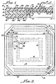
- FIG. 1 Illustrated in FIG. 1 is a single chip layer.
- the single chip layer in FIG. 1 shows a chip carrier, or substrate 10, carrying a single chip 12.
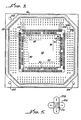
- FIG. 2 shows only one half of the chip carrier and chip, which may be symmetrical about the center line 11.
- This layer is to be assembled in a stack of chip layers, each with a mounted chip, as illustrated in FIG. 4.
- This figure shows a sectional view of one half of a complete hermetically sealed stack of integrated circuit chips, for a stack that is symmetrical about centerline 11.
- the single chip layer of FIG. 1 comprises a substrate or chip carrier, generally indicated at 10, upon which is mounted a conventional integrated circuit chip 12 having a plurality of chip connecting pads, such as pad 14 shown in FIG. 1.
- Chip carrier 10 may either be a single layer solid substrate or, as shown in FIG. 1, a multi-layer substrate formed of any suitable number of layers, such as first, second and third substrate layers 16,18 and 20.
- the carrier 10, in the embodiment illustrated in the drawings, is of generally rectangular configuration, as can be seen in FIGS. 2 and 3, and has a symmetrically and centrally located cavity 22 formed in its bottom.
- Each of the substrate layers has a pattern of electrically conductive traces formed thereon for interconnection of various elements, as will be described below.
- traces 24 are formed on the upper surface of lower layer 22
- traces 26 are formed on the upper surface of intermediate layer 18
- traces 28,30 are formed on the upper surface of upper layer 16.
- traces 28 and 30 have exposed bond finger portions 32 and 34, respectively (see FIGS. 1 and 3).
- the various substrate layers are formed of very thin (from about 1 to 10 mil thickness) dielectric ceramic, such as alumina, aluminum oxide (Al2O3), aluminum nitride (AlN), or other suitable nonconductive material.
- dielectric ceramic such as alumina, aluminum oxide (Al2O3), aluminum nitride (AlN), or other suitable nonconductive material.
- vias 40,42, and 44 Extending through the thicker part of the substrate, surrounding the cavity 22, are rows of vias, such as vias 40,42, and 44, filled with an electrically conductive material, such as a tungsten paste, for example, and extending continuously from the top side of the carrier to its bottom side.
- an electrically conductive material such as a tungsten paste, for example
- the top side of the carrier is the side that is deemed to be uppermost as viewed in FIG. 1, and the bottom side is the side that is lowermost.
- Each of the vias has a via pad, such as pads 41a and 41b, 43a and 43b, and 45a and 45b, electrically and mechanically connected to the top and bottom ends of the via, respectively.
- a continuous top side seal strip 46 and a continuous bottom side seal strip 48 Running continuously around the peripheral edge of both the top side and bottom side of the carrier substrate 10 are a continuous top side seal strip 46 and a continuous bottom side seal strip 48. Additional vias, such as a via 50, extend through the thinner part of the substrate above cavity 22 to interconnect certain of the trace patterns on different layers of the single carrier, such as for interconnection of trace 30 with trace 26.
- a very thin (in the order of a fraction of a mil in thickness) dielectric protective inner cavity layer 52 is bonded to the bottom of the cavity 22, that is, to the lowermost portion of the thin inner portion of the carrier substrate, to shield leads running along the lower surface of this portion of the substrate.
- a similar thin dielectric outer cavity cover layer 54 of a rectangular configuration for this rectangular configuration chip carrier overlies and is bonded to the uppermost layer 16 of substrate 10.
- Cover layer 54 has a peripheral edge 55 (see also FIG. 3) which is positioned to expose free ends of all of the upper layer leads 34.
- outer cavity cover layer 54 protects inner portions of leads 30 but leaves an exposed portion 34 that is available for bonding to a bond wire 58 to connecting pads 14 of the chip 12.
- the latter is mounted by a suitable adhesive (not shown) on the upper surface of cover layer 54.
- the chip may have a size equal to but preferably not greater than the dimensions of the cover layer 54 so that edges of the chip do not extend beyond, and are preferably set back somewhat from, the peripheral edge 55 of the cover layer 54.
- Chip 12 is shown in phantom lines in FIG. 3.
- All of the electrically conductive traces, all of the via pads, and all of the seal strips are preferably formed by the same process, using the same material.
- a tungsten paste is screened onto the substrate layer and then fired together with the individual substrate layer to cause the paste to solidify and to become bonded to the layer. Thereafter the fired tungsten paste is covered with a barrier layer of nickel and then a very thin outermost layer of gold (for at least the exposed areas).
- a thin coat of a high temperature reflowable solder is thereafter applied to all of the via pads and to all of the peripheral seal strips, but not to any of the other traces.
- Certain pads or bumps on the bottom of a stack to be used to mount the stack may be formed of a relatively low temperature solder, as will be described below.
- the via top and bottom pads are each elongated, having an aspect ratio of about 3:1, that is, a length of three times the width.
- the via pads are oriented so that when several carriers are stacked, as shown in FIG. 4, with the via pad at the top side of one carrier in contact with the via pad at the bottom side of an adjacent carrier to form a pair of contacting via pads, the two elongated pads of a single pair of contacting via pads are angulated with respect to one another, and preferably positioned at right angles to each other, as shown FIG. 5.
- a via pad 41a that is positioned at the top side of via 40 of a lower layer and in contact with a via pad 137b at the bottom side of an immediately higher layer.
- the vias are arranged in parallel rows on each of the four sides of the carrier cavity 22.
- a row of via pads including lower side via pad 41b is identified in FIG. 2 as via pad row 62 (extending vertically in FIG. 2).
- a row including via pad 43b is identified as vertically extending row 64
- a row of via pads including via pad 45b is identified as vertically extending row 66.
- all of the vias of these three rows have their longitudinal axes aligned in directions parallel to the extent of the several rows (e.g., vertically, as viewed in FIG. 2).
- a similar set of three via pad rows 68,70,72 are arranged in an identical pattern along the right side of the cavity 22.
- along the top and bottom side of the cavity are arranged groups of horizontally extending via rows 74,76,78 on the top side of the cavity, as viewed in FIG. 2, and horizontal via rows 80,82 and 84 on the bottom side of the cavity.
- all the vias have their longitudinal axes parallel to one another in each row and in each group of rows and parallel to the extent of the rows.
- the longitudinal axes of the vertically extending rows of vias 62,64,66,68,70,72 are all parallel to one another and perpendicular to the longitudinal axes of horizontally extending via rows 74-84.
- Each of the vias of the inner pair of rows are connected to leads buried within the thin portion of the substrate layer above the cavity, such as lead 26 (FIGS. 1 and 2) which connects to via 40 (FIG. 1) and to one of the vias 50 (FIGS. 1 and 3) extending through the thin portion of the substrate above the cavity.
- leads 26 FIG. 1 and 2 which connects to via 40 (FIG. 1) and to one of the vias 50 (FIGS. 1 and 3) extending through the thin portion of the substrate above the cavity.
- via pad 41b is connected via lead 26, on layer 18, and via 50 (through layer 16) to the lead 30 which has an end portion 34 exposed for connection to a bonding wire 58 and chip pad 14.
- a group of the vias are designated herein as cavity vias and generally indicated in FIGS. 2 and 3 by numeral 86 (which include the via 50), which, like the via 50, extend through the thin portion of the upper layer 16 for connection to different ones of leads on the surface of the upper layer 16.
- the cavity vias 86 are each connected by buried leads analogous to lead 26 to a different one of the vias in the row of vias indicted at 62 (FIG. 2).
- additional groups of cavity vias 88,90 and 92 are connected by buried leads to respective ones of the vias in outer via rows 78,72 and 84, respectively. To maintain clarity of the drawings, only some of these buried leads are shown, but the general pattern of leads is as illustrated.
- Cavity vias 86,90 and 92 all extend through the thinner portion of the substrate layer above the cavity 22 and are individually connected to respective ones of leads, such as leads 30, formed on the uppermost surface of the layer 16 above the cavity.
- leads such as leads 30, formed on the uppermost surface of the layer 16 above the cavity.
- the top of carrier 10 as illustrated in FIG. 3 merely is turned over so that the right side of the carrier, as viewed in FIG. 3, becomes the left side of the turned over carrier as viewed in FIG. 2, and the left side of the carrier as seen in FIG. 2 becomes right side of the carrier as seen in FIG. 3.
- the carrier includes three registration openings 100,102, and 104 at three different corners of the carrier.
- registration opening 100 is seen at the upper left corner, whereas the other side of this same opening is seen in the upper right corner of FIG. 2.
- opening 102 is seen in the lower right corner of FIG. 2 and in the lower left corner of FIG. 3.
- each of the cavity vias 86,88,90 and 92 are covered by a very thin (a fraction of a mil) dielectric layer 54 which covers the cavity via groups and portions of the conductive leads on the upper surface of the upper carrier layer. Also shown in FIG. 3 in phantom lines is the outline of the integrated circuit chip 12 that will be adhesively bonded to the uppermost surface of the thin dielectric cover layer 54.
- a generally rectangular ring shaped cover layer 110 also formed of a very thin dielectric material, such as a ceramic, alumina or the like, covers the uppermost surface of the upper layer of carrier 10 and extends completely around the outer cavity cover layer 54.
- the inner periphery 112 of the ring shaped cover layer is spaced from the outer periphery 114 of the outer cavity cover layer 54 so as to expose portions of the traces collectively indicated at 28 and 30. As indicated above, these exposed portions of the traces are arranged for connection of bond wires, such as wire bond 58, that are also bonded to the chip connecting pads 14.
- the exposed traces, such as trace 38 are connected by leads 28 (FIGS.
- FIG. 3 also shows the groups of three rows of vias on each side of the carrier (actually only the via pads on the upper sides of the vias are seen in the figure) with via rows 62b,64b,66b corresponding respectively to via rows 62,64, and 66 of FIG. 2.
- any one via of the vertically extending rows has a vertically oriented pad on its bottom side (vertical as seen in FIG. 2) and the same via has a horizontally oriented via (as seen in FIG. 3) on its top side.
- each via has a top side pad oriented in one direction and a bottom side pad oriented in a perpendicular direction, as can be seen from the illustrations of FIGS. 2 and 3.
- the via pads of the inner rows of the top side pads of via rows 64 and 66 are connected by traces, such as trace 28, partially buried beneath the ring shaped cover layer 110 and having exposed end portions, such as exposed end portion 32 of trace 28. Wire bonds from the individual chip connecting pads 14 are connected respectively to different ones of the exposed ends 32,34, etc. of the partially buried traces, which are connected at their other ends to individual ones of the cavity vias that extend through the upper carrier layer.
- the continuous seal strip 48, on the bottom side of the substrate, and strip 46, on the top side of the substrate, extend around the entire periphery of both top and bottom sides of the substrate.
- FIG. 4 Illustrated in FIG. 4 is an exemplary stack formed of three intermediate chip layers 10,120, and 130, each of which may be identical to the single chip layer shown in FIGS. 1, 2 and 3, and including a lid or uppermost layer 132 and a base or lower layer 134.
- the upper layer 132 is identical to the intermediate chip layers 10,120 and 130 except for the fact that no chip is mounted on its upper surface and none of the connecting leads necessary for connection of the chips pads are needed or used. However, this upper layer also includes electrically conductive tungsten filled vias 136,138 and 140, having top and bottom pads 137a and 137b, 139a and 139b, and 141a and 141b on top and bottom sides of the respective vias 136,138,140.
- the uppermost layer or lid 132 also is formed with a continuous peripheral seal 144 on its lower surface. No such seal is needed, of course, on its upper surface.
- the lowermost layer or base 134 is identical to the intermediate layers 10,120 and 130. Its three electrically conductive tungsten filled vias 150,152, and 154 are provided with top side via pads just the same as are provided for the intermediate layers 10,120 and 130 but may be provided with smaller pin type via pads 156,158, and 160, respectively, that are specifically configured and arranged to be received in solder wells (not shown) on a PC board or other mounting substrate for making physical and electrical connection of the stack to the mounting substrate.
- the via pads of the successive layers are in physical, mechanical and electrical contact with one another in the stack. So too the peripheral seals on top and bottom sides of adjacent layers are in hermetically sealing contact with one another to provide a complete hermetic seal for the entire package.
- Each ceramic carrier of one or multiple layers with vias, traces and registration openings is formed.
- the several traces are formed by screened-on tungsten paste fired together with the layer and then covered with a nickel barrier and a thin gold layer, where appropriate.
- the vias are filled with a suitable conductive compound, such as a tungsten paste, which is fired together with the individual layers, the tungsten traces, seal strips and via pads.
- the carrier substrate has applied to its upper surface the thin dielectric ceramic inner and outer cover layers 52,54 and ring shaped cover layer 110, which are suitably bonded thereto, and, as previously mentioned, may have a thickness of a fraction of a mil.
- each carrier is now available for mounting of its die integrated circuit chip.
- the chip is adhesively secured to (as by an epoxy, for example) the cover layer 54 and its chip connecting pads wire bonded to different ones of the exposed traces 32,34.
- the chip and its carrier may be completely tested to ensure proper operation before the chip and its carrier are assembled in a stack.
- the several chip layers comprising the carrier and chip, are then stacked on a stacking fixture or stacking base with all the sealing strips in contact with one another and with top via pads of one layer in contact with and orthogonally oriented relative to the bottom via pads of the next upper layer.
- the stack is assembled on a group of three mutually parallel vertical alignment pins (not shown) fixed on a fixed stacking fixture base and protruding vertically through the respective alignment openings 100,102 and 104 of each of the carriers and stack layers, including the lid 132 and the lower layer 134.
- the stack, held with its several carriers mutually aligned by the alignment pins, is placed in an oven and weighted to press the layers against one another.
- the assembly is heated to cause the solder to soften and/or melt and to form solder joints between connecting seal strips and mutually contacting via pads to provide strong, reliable, mechanical, electrical and thermal connections between the stacked carriers.
- each of these openings is elongated and has a longitudinal axis. The longitudinal axis of each opening intersects the geometric center of the carrier layer.
- Each carrier layer will thermally expand or contract equally in all directions from its geometric center, and thus the elongated registration openings, elongated in the direction of a line to the geometric center, allow such a thermally induced change in dimension without loss of alignment of one layer with the next. Since all of the openings are referenced to the geometric center of the layer rather than to any single edge, there is required a tolerance of only one-half of that which would be required if the registration openings are referenced from an edge of the layer. Thus, this unique arrangement of elongated registration openings, aligned with the geometric center of the carriers, greatly eases dimensional tolerance in manufacture of various layers, simplifies the assembly procedure and decreases cost of assembly.
- the stack Having fired the stack, it is removed from the oven and the complete hermetically sealed package is available for incorporation and/or mounting of the stacks by means of the solder bumps 156,158,160, etc. to another device, such as a printed wiring board or a multi-chip module or similar structure.
- the reflow solder employed for the vias pads and seal strips is a high temperature solder, having melting point that is as much as 70° higher than the low temperature solder employed for the mounting solder bumps or pads 156,158,160 (FIG. 4). Accordingly, when the latter are softened or melted for connection and mounting of the entire stack, the integrity of the stack internal solder interconnections is not affected.
- the solder bumps 156,158,160 may be positioned in wells on the printed wiring board or the multi-chip module and reflowed to provide mechanical and electrical connection.
- solder interconnections also provide good thermal paths throughout the entire length of the stack from top to bottom and also from inside to outside because of the close proximity of one solder pad to another and to the perimetral hermetic seal.
- tape automated bonding structures may be attached to the lower solder bumps 156,159,160, with the tape automated bonding structures extending past the edges of the stack so that outer leads of the bonding structure may then be connected to pads on a printed wiring board or multi-chip module.
- the thin dielectric ring-shaped cover layer 110 that surrounds each of the via pads acts as a solder dam to prevent flowing or wicking of solder from one pad to another or from one pad to exposed leads of the traces.
- This dielectric ring-shaped layer 110 acts as a solder dam, at least in part because it effectively prevents flow of solder along its surface.
- FIG. 5 illustrates a via pad, such as pad 41a of the top side of via 40 of a lower carrier layer and a corresponding contacting via pad, such as pad 137b at the bottom side of an immediately adjacent relatively upper layer.
- each of the via pads has a length of approximately three times its width, with its width being approximately equal to the diameter of the associated via, which is in the order of about 5 mils.
- This contact area is nominally a square with an equal length of non-contacting via pad extending on all four sides of this square.
- the contacting area 170 still remains as a square having the same area, until the misalignment becomes greater than one-third the full length of the elongated pad. If the pads were of equal or comparable shape and size to one another, any such misalignment would cause an overlap in the contacting of the pads and at least a partial relative displacement, and thereby would significantly decrease the contacting area. Accordingly, the orthogonal orientation of each pair of contacting pads provides for a uniform area of contact, even in the presence of some misalignment, and thereby ensures that each contacting area provides a uniform electrically conductive area, mechanical bond strength, and thermal path area.
- the areas of the pads outside of the contacting shaded area 170 will direct any excess flow of contacting solder and confine it to the area of the pad. In other words, any excess flowing solder which may occur during the reflow process will flow in the direction of the arrows shown in FIG. 5 and be confined to the pad area.
- the elongated pads do not significantly impact upon available area for positioning of traces since portions of some of the traces may be readily routed beneath the areas of the pads that project beyond the common contacting or shaded area.
- Mechanical strength is improved because mechanical failure generally occurs at the weakest mechanical point, that connecting area in which the solder interconnection from one via pad to the other has a decreased area because of misregistration.
- Electrical uniformity occurs because of the uniformity of the contacting area and similarly thermal conductivity from pad to pad, and thereby from top to bottom of the entire stack, is increased for each thermal path that extends through aligned vias from top to bottom of the stack.
- Input/output connections to the stack are made through the via pads at the bottom 156,158 and 160, and further input/output connections are made to the via pads 137a,139a and 141a on the lid or uppermost layer 132.
- Each carrier is connected to all other carriers, and to external input/output connections (e.g., the outermost via pads) through the many vias which extend completely through the stack and all carriers.
- the number of these input/output connections that is the total number of via pads available in any one horizontal outside layer (namely the uppermost and lowermost layers), is very large, and thus a significant increase in the number of input/output connections to the stacked chips is available with the arrangement of the present invention.
- a stack embodying principles of the present invention will exhibit dramatic decreases in size, weight and power.
- the decrease in size and weight is due to the decreased overall volume of the stack, which allows utilization of all of the chip pads and provides a large number of input/output connections. The number of these connections is not constrained or restricted by the area of the side of the stack. Further, because of the compact arrangement and the mode of interconnection of chips from one layer to another, the total length of leads employed internally of the stack is less, and, importantly, the length of individual leads is less. Because of this decrease in lead length, the stray capacitance of the package is greatly reduced. Stray or distributed capacitance, as is well known, may cause power losses in excess of fifty percent.
- the power loss is related to the stray or distributed capacitance of the circuit, performance is enhanced by greatly decreased power loss. Further, the shorter length of leads not only decreases the stray capacitance, it decreases the travel time of signals within the package, thereby enhancing speed. Accordingly, circuit performance is enhanced because of the decrease in capacitance and the decreased time of travel of signals within the package allowing greater component and system operating speeds.
- Total thickness of each individual carrier may vary between 18 and 70 mils depending upon the number of layers in the carrier substrate and the thickness of the integrated circuit chips which are mounted on each carrier substrate. Chips vary in size and thickness and may have a thickness of between 5 and 25 mils and a rectangular configuration of from about 0.50 to 1.0 inches or more per side. A total carrier thickness is in the order of about 10 to 12 mils greater than the thickness of the chip that it carries. Note that each cavity of one layer carrier partially receives the chip mounted on the top side of the next lower carrier and also provides some space for the bonding wire.
- a stack may have a height of up to 50 layers (e.g., 50 carriers, each with a chip thereon), with about a total of 0.020 inches for each chip layer (e.g., carrier plus chip). If a stack is laid on its side, the total number of layers may be significantly greater.
- the carrier substrate has a total thickness of 0.027 inches, with the center portion of the substrate, above the cavity, having a thickness of 0.009 inches.
- the outer carrier dimensions in one example, are 0.790 x 0.790, and the cavity is 0.535 x 0.485 inches.
- flip-chip mounting may be employed in which the chip is turned upside-down with its connecting pads facing the substrate on which it is mounted.
- the substrate has appropriate connecting pads for electrically connecting to the flipped over chip.
- the various traces can either be screened on or plated on.
- the flip-chip may be connected using either tape automated bonding or solder bumps.
- the solder employed on the high temperature solder bumps is a fluxless solder to prevent parasitic effects that may result from the use of flux.
- the stack of layers provides an alignment of vias that extends from top to bottom of the stack to provide a continuous electrical and thermal path.
- the various chip leads and traces on each carrier, and on each layer of each multi-layer carrier may be connected to one or another or any group of the vias so that any chip of the stack may be connected to leads on its same carrier and also to leads connecting to chips on other carriers. Accordingly, chips in any one stack may be interconnected to one another as desired or may be simply coupled to input/output via connecting pads without connection to any other chip in the stack.
- the sealing strip is essentially made in the same fashion as are all of the traces and via pads, excepting that it is additionally coated with a reflow solder that is not applied to the conductive traces, the sealing is greatly simplified without compromise of sealing effectivity. No special types of materials or sealing rings are needed to be fabricated or assembled.
Applications Claiming Priority (2)
| Application Number | Priority Date | Filing Date | Title |
|---|---|---|---|
| US08/326,455 US5579207A (en) | 1994-10-20 | 1994-10-20 | Three-dimensional integrated circuit stacking |
| US326455 | 1994-10-20 |
Publications (2)
| Publication Number | Publication Date |
|---|---|
| EP0708484A1 true EP0708484A1 (de) | 1996-04-24 |
| EP0708484B1 EP0708484B1 (de) | 2001-09-26 |
Family
ID=23272291
Family Applications (1)
| Application Number | Title | Priority Date | Filing Date |
|---|---|---|---|
| EP95307398A Expired - Lifetime EP0708484B1 (de) | 1994-10-20 | 1995-10-18 | Dreidimensionaler integrierter Schaltungsstapel |
Country Status (5)
| Country | Link |
|---|---|
| US (1) | US5579207A (de) |
| EP (1) | EP0708484B1 (de) |
| JP (1) | JP2703745B2 (de) |
| DE (1) | DE69522887T2 (de) |
| IL (1) | IL115637A (de) |
Cited By (6)
| Publication number | Priority date | Publication date | Assignee | Title |
|---|---|---|---|---|
| EP0807369A1 (de) * | 1995-01-23 | 1997-11-19 | Irvine Sensors Corporation | Stapelmodule und mehrfachmodul-zusammenbau |
| KR19990051841A (ko) * | 1997-12-20 | 1999-07-05 | 김영환 | 칩 스케일 패키지 및 그 제조방법 |
| GB2337852A (en) * | 1998-05-26 | 1999-12-01 | Nec Corp | Multichip module |
| WO2004006333A1 (en) * | 2002-07-04 | 2004-01-15 | Koninklijke Philips Electronics N.V. | Multi electric device package |
| US6780672B2 (en) * | 2000-01-31 | 2004-08-24 | Lockheed Martin Corporation | Micro eletro-mechanical component and system architecture |
| EP2393345A1 (de) * | 2010-05-04 | 2011-12-07 | Vincotech Holdings S.a.r.l. | Schaltungsträger mit Aussparung zum Aufnehmen elektronischer Bauteile, die mit einer Leiterplatine in Kontakt kommen |
Families Citing this family (163)
| Publication number | Priority date | Publication date | Assignee | Title |
|---|---|---|---|---|
| KR100437436B1 (ko) * | 1994-03-18 | 2004-07-16 | 히다치 가세고교 가부시끼가이샤 | 반도체패키지의제조법및반도체패키지 |
| US5468917A (en) * | 1994-03-23 | 1995-11-21 | International Business Machines Corporation | Circuitized structure including flexible circuit with elastomeric member bonded thereto |
| JPH09214097A (ja) * | 1996-02-06 | 1997-08-15 | Toshiba Corp | プリント回路基板 |
| US5914534A (en) * | 1996-05-03 | 1999-06-22 | Ford Motor Company | Three-dimensional multi-layer molded electronic device and method for manufacturing same |
| US5748452A (en) * | 1996-07-23 | 1998-05-05 | International Business Machines Corporation | Multi-electronic device package |
| KR100422608B1 (ko) * | 1997-05-10 | 2004-06-04 | 삼성전자주식회사 | 적층칩패키지 |
| US6195268B1 (en) * | 1997-06-09 | 2001-02-27 | Floyd K. Eide | Stacking layers containing enclosed IC chips |
| US5790384A (en) * | 1997-06-26 | 1998-08-04 | International Business Machines Corporation | Bare die multiple dies for direct attach |
| US6070531A (en) * | 1997-07-22 | 2000-06-06 | Autoliv Asp, Inc. | Application specific integrated circuit package and initiator employing same |
| KR100280398B1 (ko) * | 1997-09-12 | 2001-02-01 | 김영환 | 적층형 반도체 패키지 모듈의 제조 방법 |
| US6099677A (en) * | 1998-02-13 | 2000-08-08 | Merrimac Industries, Inc. | Method of making microwave, multifunction modules using fluoropolymer composite substrates |
| JP3563604B2 (ja) * | 1998-07-29 | 2004-09-08 | 株式会社東芝 | マルチチップ半導体装置及びメモリカード |
| US6668242B1 (en) * | 1998-09-25 | 2003-12-23 | Infineon Technologies North America Corp. | Emulator chip package that plugs directly into the target system |
| US6190425B1 (en) | 1998-11-03 | 2001-02-20 | Zomaya Group, Inc. | Memory bar and related circuits and methods |
| US6295220B1 (en) | 1998-11-03 | 2001-09-25 | Zomaya Group, Inc. | Memory bar and related circuits and methods |
| US6205032B1 (en) * | 1999-03-16 | 2001-03-20 | Cts Corporation | Low temperature co-fired ceramic with improved registration |
| US6268568B1 (en) * | 1999-05-04 | 2001-07-31 | Anam Semiconductor, Inc. | Printed circuit board with oval solder ball lands for BGA semiconductor packages |
| US6593645B2 (en) * | 1999-09-24 | 2003-07-15 | United Microelectronics Corp. | Three-dimensional system-on-chip structure |
| US6392428B1 (en) * | 1999-11-16 | 2002-05-21 | Eaglestone Partners I, Llc | Wafer level interposer |
| US6627864B1 (en) | 1999-11-22 | 2003-09-30 | Amkor Technology, Inc. | Thin image sensor package |
| US6396043B1 (en) | 1999-11-22 | 2002-05-28 | Amkor Technology, Inc. | Thin image sensor package fabrication method |
| JP2001177051A (ja) * | 1999-12-20 | 2001-06-29 | Toshiba Corp | 半導体装置及びシステム装置 |
| US7102892B2 (en) * | 2000-03-13 | 2006-09-05 | Legacy Electronics, Inc. | Modular integrated circuit chip carrier |
| US6713854B1 (en) | 2000-10-16 | 2004-03-30 | Legacy Electronics, Inc | Electronic circuit module with a carrier having a mounting pad array |
| US6571466B1 (en) | 2000-03-27 | 2003-06-03 | Amkor Technology, Inc. | Flip chip image sensor package fabrication method |
| US6612852B1 (en) | 2000-04-13 | 2003-09-02 | Molex Incorporated | Contactless interconnection system |
| US6362972B1 (en) * | 2000-04-13 | 2002-03-26 | Molex Incorporated | Contactless interconnection system |
| US6812048B1 (en) | 2000-07-31 | 2004-11-02 | Eaglestone Partners I, Llc | Method for manufacturing a wafer-interposer assembly |
| US6537831B1 (en) * | 2000-07-31 | 2003-03-25 | Eaglestone Partners I, Llc | Method for selecting components for a matched set using a multi wafer interposer |
| JP3874062B2 (ja) * | 2000-09-05 | 2007-01-31 | セイコーエプソン株式会社 | 半導体装置 |
| US6815712B1 (en) | 2000-10-02 | 2004-11-09 | Eaglestone Partners I, Llc | Method for selecting components for a matched set from a wafer-interposer assembly |
| US7337522B2 (en) * | 2000-10-16 | 2008-03-04 | Legacy Electronics, Inc. | Method and apparatus for fabricating a circuit board with a three dimensional surface mounted array of semiconductor chips |
| US6686657B1 (en) | 2000-11-07 | 2004-02-03 | Eaglestone Partners I, Llc | Interposer for improved handling of semiconductor wafers and method of use of same |
| US6342406B1 (en) | 2000-11-15 | 2002-01-29 | Amkor Technology, Inc. | Flip chip on glass image sensor package fabrication method |
| US6849916B1 (en) | 2000-11-15 | 2005-02-01 | Amkor Technology, Inc. | Flip chip on glass sensor package |
| US6524885B2 (en) * | 2000-12-15 | 2003-02-25 | Eaglestone Partners I, Llc | Method, apparatus and system for building an interposer onto a semiconductor wafer using laser techniques |
| US20020076854A1 (en) * | 2000-12-15 | 2002-06-20 | Pierce John L. | System, method and apparatus for constructing a semiconductor wafer-interposer using B-Stage laminates |
| US6529022B2 (en) | 2000-12-15 | 2003-03-04 | Eaglestone Pareners I, Llc | Wafer testing interposer for a conventional package |
| US20020078401A1 (en) * | 2000-12-15 | 2002-06-20 | Fry Michael Andrew | Test coverage analysis system |
| US6673653B2 (en) * | 2001-02-23 | 2004-01-06 | Eaglestone Partners I, Llc | Wafer-interposer using a ceramic substrate |
| US6469375B2 (en) * | 2001-02-28 | 2002-10-22 | William F. Beausoleil | High bandwidth 3D memory packaging technique |
| KR100897314B1 (ko) * | 2001-03-14 | 2009-05-14 | 레가시 일렉트로닉스, 인크. | 반도체 칩의 3차원 표면 실장 어레이를 갖는 회로 기판을 제조하기 위한 방법 및 장치 |
| US6979892B2 (en) * | 2001-04-25 | 2005-12-27 | Delphi Technologies, Inc. | Laminated co-fired sandwiched element for non-thermal plasma reactor |
| US6586826B1 (en) | 2001-06-13 | 2003-07-01 | Amkor Technology, Inc. | Integrated circuit package having posts for connection to other packages and substrates |
| US6476476B1 (en) * | 2001-08-16 | 2002-11-05 | Amkor Technology, Inc. | Integrated circuit package including pin and barrel interconnects |
| US20040173894A1 (en) * | 2001-09-27 | 2004-09-09 | Amkor Technology, Inc. | Integrated circuit package including interconnection posts for multiple electrical connections |
| US20050051859A1 (en) * | 2001-10-25 | 2005-03-10 | Amkor Technology, Inc. | Look down image sensor package |
| JP3655242B2 (ja) * | 2002-01-04 | 2005-06-02 | 株式会社東芝 | 半導体パッケージ及び半導体実装装置 |
| ES2440770T3 (es) * | 2002-02-26 | 2014-01-30 | Legacy Electronics, Inc. | Un soporte modular de microplaquetas de circuitos integrados |
| US7754976B2 (en) * | 2002-04-15 | 2010-07-13 | Hamilton Sundstrand Corporation | Compact circuit carrier package |
| US6711029B2 (en) * | 2002-05-21 | 2004-03-23 | Cts Corporation | Low temperature co-fired ceramic with improved shrinkage control |
| JP3778445B2 (ja) * | 2003-03-27 | 2006-05-24 | 富士通株式会社 | 半導体装置 |
| US7030486B1 (en) * | 2003-05-29 | 2006-04-18 | Marshall Paul N | High density integrated circuit package architecture |
| US6768189B1 (en) * | 2003-06-04 | 2004-07-27 | Northrop Grumman Corporation | High power chip scale package |
| US7191516B2 (en) * | 2003-07-16 | 2007-03-20 | Maxwell Technologies, Inc. | Method for shielding integrated circuit devices |
| US7042307B2 (en) * | 2003-09-10 | 2006-05-09 | Merrimac Industries, Inc. | Coupler resource module |
| JP4175241B2 (ja) * | 2003-11-07 | 2008-11-05 | セイコーエプソン株式会社 | 半導体装置の製造方法 |
| JP3751625B2 (ja) | 2004-06-29 | 2006-03-01 | 新光電気工業株式会社 | 貫通電極の製造方法 |
| KR100688500B1 (ko) * | 2004-09-06 | 2007-03-02 | 삼성전자주식회사 | 반도체 칩 보호용 더미 패키지 기판을 구비하는 멀티스택패키지와 그 제조 방법 |
| KR100608289B1 (ko) * | 2004-10-01 | 2006-08-09 | 엘지이노텍 주식회사 | 프론트 엔드 모듈 |
| JP2006165320A (ja) * | 2004-12-08 | 2006-06-22 | Matsushita Electric Ind Co Ltd | 半導体積層モジュールとその製造方法 |
| JP4433298B2 (ja) * | 2004-12-16 | 2010-03-17 | パナソニック株式会社 | 多段構成半導体モジュール |
| WO2006076381A2 (en) | 2005-01-12 | 2006-07-20 | Legacy Electronics, Inc. | Radial circuit board, system, and methods |
| US7279786B2 (en) * | 2005-02-04 | 2007-10-09 | Stats Chippac Ltd. | Nested integrated circuit package on package system |
| EP1863087A4 (de) | 2005-03-17 | 2010-12-22 | Panasonic Corp | Modul-board |
| US7364945B2 (en) * | 2005-03-31 | 2008-04-29 | Stats Chippac Ltd. | Method of mounting an integrated circuit package in an encapsulant cavity |
| US7354800B2 (en) * | 2005-04-29 | 2008-04-08 | Stats Chippac Ltd. | Method of fabricating a stacked integrated circuit package system |
| US7746656B2 (en) * | 2005-05-16 | 2010-06-29 | Stats Chippac Ltd. | Offset integrated circuit package-on-package stacking system |
| US7518224B2 (en) * | 2005-05-16 | 2009-04-14 | Stats Chippac Ltd. | Offset integrated circuit package-on-package stacking system |
| US8643163B2 (en) * | 2005-08-08 | 2014-02-04 | Stats Chippac Ltd. | Integrated circuit package-on-package stacking system and method of manufacture thereof |
| US20070108583A1 (en) * | 2005-08-08 | 2007-05-17 | Stats Chippac Ltd. | Integrated circuit package-on-package stacking system |
| US8389867B2 (en) * | 2005-09-30 | 2013-03-05 | Ibiden Co., Ltd. | Multilayered circuit substrate with semiconductor device incorporated therein |
| US7768125B2 (en) * | 2006-01-04 | 2010-08-03 | Stats Chippac Ltd. | Multi-chip package system |
| US7456088B2 (en) * | 2006-01-04 | 2008-11-25 | Stats Chippac Ltd. | Integrated circuit package system including stacked die |
| US7750482B2 (en) * | 2006-02-09 | 2010-07-06 | Stats Chippac Ltd. | Integrated circuit package system including zero fillet resin |
| US8704349B2 (en) * | 2006-02-14 | 2014-04-22 | Stats Chippac Ltd. | Integrated circuit package system with exposed interconnects |
| US7435619B2 (en) * | 2006-02-14 | 2008-10-14 | Stats Chippac Ltd. | Method of fabricating a 3-D package stacking system |
| JP2007234782A (ja) * | 2006-02-28 | 2007-09-13 | Toyota Industries Corp | 複合回路基板 |
| US7903417B2 (en) * | 2006-10-10 | 2011-03-08 | Deere & Company | Electrical circuit assembly for high-power electronics |
| US20080084671A1 (en) * | 2006-10-10 | 2008-04-10 | Ronnie Dean Stahlhut | Electrical circuit assembly for high-power electronics |
| KR100817073B1 (ko) * | 2006-11-03 | 2008-03-26 | 삼성전자주식회사 | 휨방지용 보강부재가 기판에 연결된 반도체 칩 스택 패키지 |
| JP5068990B2 (ja) * | 2006-12-26 | 2012-11-07 | 新光電気工業株式会社 | 電子部品内蔵基板 |
| US8163600B2 (en) * | 2006-12-28 | 2012-04-24 | Stats Chippac Ltd. | Bridge stack integrated circuit package-on-package system |
| TWI335070B (en) * | 2007-03-23 | 2010-12-21 | Advanced Semiconductor Eng | Semiconductor package and the method of making the same |
| KR100874926B1 (ko) * | 2007-06-07 | 2008-12-19 | 삼성전자주식회사 | 스택 모듈, 이를 포함하는 카드 및 이를 포함하는 시스템 |
| US7713891B1 (en) * | 2007-06-19 | 2010-05-11 | Milliken & Company | Flame resistant fabrics and process for making |
| DE102007041892A1 (de) * | 2007-09-04 | 2009-03-05 | Robert Bosch Gmbh | Elektrische Schaltanordnung mit einem MID-Schaltungsträger und einer damit verbundenen Verbindungsschnittstelle |
| US8124451B2 (en) * | 2007-09-21 | 2012-02-28 | Stats Chippac Ltd. | Integrated circuit packaging system with interposer |
| US7933128B2 (en) * | 2007-10-10 | 2011-04-26 | Epson Toyocom Corporation | Electronic device, electronic module, and methods for manufacturing the same |
| US8399973B2 (en) * | 2007-12-20 | 2013-03-19 | Mosaid Technologies Incorporated | Data storage and stackable configurations |
| US7791175B2 (en) * | 2007-12-20 | 2010-09-07 | Mosaid Technologies Incorporated | Method for stacking serially-connected integrated circuits and multi-chip device made from same |
| EP2250862B1 (de) | 2008-02-13 | 2019-06-12 | Cameron International Corporation | Anordnungssystem |
| US8258015B2 (en) * | 2008-02-22 | 2012-09-04 | Stats Chippac Ltd. | Integrated circuit package system with penetrable film adhesive |
| JP5175616B2 (ja) * | 2008-05-23 | 2013-04-03 | シャープ株式会社 | 半導体装置およびその製造方法 |
| TWI473553B (zh) * | 2008-07-03 | 2015-02-11 | Advanced Semiconductor Eng | 晶片封裝結構 |
| US8304869B2 (en) * | 2008-08-01 | 2012-11-06 | Stats Chippac Ltd. | Fan-in interposer on lead frame for an integrated circuit package on package system |
| US8339474B2 (en) * | 2008-08-20 | 2012-12-25 | Freescale Semiconductor, Inc. | Gain controlled threshold in denoising filter for image signal processing |
| US7836586B2 (en) * | 2008-08-21 | 2010-11-23 | National Semiconductor Corporation | Thin foil semiconductor package |
| US20100171206A1 (en) * | 2009-01-07 | 2010-07-08 | Chi-Chih Chu | Package-on-Package Device, Semiconductor Package, and Method for Manufacturing The Same |
| TWI499024B (zh) * | 2009-01-07 | 2015-09-01 | Advanced Semiconductor Eng | 堆疊式多封裝構造裝置、半導體封裝構造及其製造方法 |
| US8012797B2 (en) * | 2009-01-07 | 2011-09-06 | Advanced Semiconductor Engineering, Inc. | Method for forming stackable semiconductor device packages including openings with conductive bumps of specified geometries |
| US7894230B2 (en) * | 2009-02-24 | 2011-02-22 | Mosaid Technologies Incorporated | Stacked semiconductor devices including a master device |
| JP2011029535A (ja) * | 2009-07-29 | 2011-02-10 | Elpida Memory Inc | 半導体装置 |
| TWI469283B (zh) * | 2009-08-31 | 2015-01-11 | Advanced Semiconductor Eng | 封裝結構以及封裝製程 |
| US10202720B2 (en) | 2009-10-21 | 2019-02-12 | Milliken & Company | Flame resistant textile |
| US8198131B2 (en) | 2009-11-18 | 2012-06-12 | Advanced Semiconductor Engineering, Inc. | Stackable semiconductor device packages |
| US8304888B2 (en) * | 2009-12-22 | 2012-11-06 | Fairchild Semiconductor Corporation | Integrated circuit package with embedded components |
| US8432031B1 (en) * | 2009-12-22 | 2013-04-30 | Western Digital Technologies, Inc. | Semiconductor die including a current routing line having non-metallic slots |
| TWI408785B (zh) | 2009-12-31 | 2013-09-11 | Advanced Semiconductor Eng | 半導體封裝結構 |
| US8115260B2 (en) | 2010-01-06 | 2012-02-14 | Fairchild Semiconductor Corporation | Wafer level stack die package |
| US8569894B2 (en) | 2010-01-13 | 2013-10-29 | Advanced Semiconductor Engineering, Inc. | Semiconductor package with single sided substrate design and manufacturing methods thereof |
| TWI419283B (zh) | 2010-02-10 | 2013-12-11 | Advanced Semiconductor Eng | 封裝結構 |
| US9496152B2 (en) * | 2010-03-12 | 2016-11-15 | STATS ChipPAC Pte. Ltd. | Carrier system with multi-tier conductive posts and method of manufacture thereof |
| US7928552B1 (en) | 2010-03-12 | 2011-04-19 | Stats Chippac Ltd. | Integrated circuit packaging system with multi-tier conductive interconnects and method of manufacture thereof |
| TWI411075B (zh) | 2010-03-22 | 2013-10-01 | Advanced Semiconductor Eng | 半導體封裝件及其製造方法 |
| US8278746B2 (en) | 2010-04-02 | 2012-10-02 | Advanced Semiconductor Engineering, Inc. | Semiconductor device packages including connecting elements |
| US8624374B2 (en) | 2010-04-02 | 2014-01-07 | Advanced Semiconductor Engineering, Inc. | Semiconductor device packages with fan-out and with connecting elements for stacking and manufacturing methods thereof |
| JP5206822B2 (ja) | 2010-07-09 | 2013-06-12 | 株式会社デンソー | 半導体装置 |
| US8253234B2 (en) | 2010-10-28 | 2012-08-28 | International Business Machines Corporation | Optimized semiconductor packaging in a three-dimensional stack |
| US8405998B2 (en) | 2010-10-28 | 2013-03-26 | International Business Machines Corporation | Heat sink integrated power delivery and distribution for integrated circuits |
| US8427833B2 (en) | 2010-10-28 | 2013-04-23 | International Business Machines Corporation | Thermal power plane for integrated circuits |
| TWI451546B (zh) | 2010-10-29 | 2014-09-01 | Advanced Semiconductor Eng | 堆疊式封裝結構、其封裝結構及封裝結構之製造方法 |
| TWI445155B (zh) | 2011-01-06 | 2014-07-11 | Advanced Semiconductor Eng | 堆疊式封裝結構及其製造方法 |
| KR101828386B1 (ko) * | 2011-02-15 | 2018-02-13 | 삼성전자주식회사 | 스택 패키지 및 그의 제조 방법 |
| US9171792B2 (en) | 2011-02-28 | 2015-10-27 | Advanced Semiconductor Engineering, Inc. | Semiconductor device packages having a side-by-side device arrangement and stacking functionality |
| US8654541B2 (en) | 2011-03-24 | 2014-02-18 | Toyota Motor Engineering & Manufacturing North America, Inc. | Three-dimensional power electronics packages |
| US8697457B1 (en) * | 2011-06-22 | 2014-04-15 | Bae Systems Information And Electronic Systems Integration Inc. | Devices and methods for stacking individually tested devices to form multi-chip electronic modules |
| US8624359B2 (en) | 2011-10-05 | 2014-01-07 | Taiwan Semiconductor Manufacturing Company, Ltd. | Wafer level chip scale package and method of manufacturing the same |
| JP2013115214A (ja) * | 2011-11-28 | 2013-06-10 | Shinko Electric Ind Co Ltd | 半導体装置、半導体素子、及び半導体装置の製造方法 |
| US8680684B2 (en) | 2012-01-09 | 2014-03-25 | Invensas Corporation | Stackable microelectronic package structures |
| US9888568B2 (en) * | 2012-02-08 | 2018-02-06 | Crane Electronics, Inc. | Multilayer electronics assembly and method for embedding electrical circuit components within a three dimensional module |
| US9947609B2 (en) * | 2012-03-09 | 2018-04-17 | Honeywell International Inc. | Integrated circuit stack |
| CN103681365B (zh) * | 2012-08-31 | 2016-08-10 | 宏启胜精密电子(秦皇岛)有限公司 | 层叠封装结构及其制作方法 |
| US8933540B2 (en) | 2013-02-28 | 2015-01-13 | International Business Machines Corporation | Thermal via for 3D integrated circuits structures |
| USD758372S1 (en) | 2013-03-13 | 2016-06-07 | Nagrastar Llc | Smart card interface |
| USD759022S1 (en) * | 2013-03-13 | 2016-06-14 | Nagrastar Llc | Smart card interface |
| TWI504320B (zh) * | 2014-06-17 | 2015-10-11 | 矽品精密工業股份有限公司 | 線路結構及其製法 |
| US9472878B2 (en) * | 2015-01-16 | 2016-10-18 | Tyco Electronics Corporation | Electrical cable connector having a two-dimensional array of mating interfaces |
| US9230726B1 (en) | 2015-02-20 | 2016-01-05 | Crane Electronics, Inc. | Transformer-based power converters with 3D printed microchannel heat sink |
| US9548277B2 (en) | 2015-04-21 | 2017-01-17 | Honeywell International Inc. | Integrated circuit stack including a patterned array of electrically conductive pillars |
| USD864968S1 (en) | 2015-04-30 | 2019-10-29 | Echostar Technologies L.L.C. | Smart card interface |
| US10178786B2 (en) | 2015-05-04 | 2019-01-08 | Honeywell International Inc. | Circuit packages including modules that include at least one integrated circuit |
| US9741644B2 (en) | 2015-05-04 | 2017-08-22 | Honeywell International Inc. | Stacking arrangement for integration of multiple integrated circuits |
| US10600691B2 (en) | 2016-10-07 | 2020-03-24 | Xcelsis Corporation | 3D chip sharing power interconnect layer |
| US10600780B2 (en) | 2016-10-07 | 2020-03-24 | Xcelsis Corporation | 3D chip sharing data bus circuit |
| US10672745B2 (en) | 2016-10-07 | 2020-06-02 | Xcelsis Corporation | 3D processor |
| US10600735B2 (en) | 2016-10-07 | 2020-03-24 | Xcelsis Corporation | 3D chip sharing data bus |
| US10593667B2 (en) * | 2016-10-07 | 2020-03-17 | Xcelsis Corporation | 3D chip with shielded clock lines |
| US10672663B2 (en) | 2016-10-07 | 2020-06-02 | Xcelsis Corporation | 3D chip sharing power circuit |
| US10580735B2 (en) * | 2016-10-07 | 2020-03-03 | Xcelsis Corporation | Stacked IC structure with system level wiring on multiple sides of the IC die |
| US10672743B2 (en) | 2016-10-07 | 2020-06-02 | Xcelsis Corporation | 3D Compute circuit with high density z-axis interconnects |
| US11176450B2 (en) | 2017-08-03 | 2021-11-16 | Xcelsis Corporation | Three dimensional circuit implementing machine trained network |
| US10580757B2 (en) * | 2016-10-07 | 2020-03-03 | Xcelsis Corporation | Face-to-face mounted IC dies with orthogonal top interconnect layers |
| US10672744B2 (en) | 2016-10-07 | 2020-06-02 | Xcelsis Corporation | 3D compute circuit with high density Z-axis interconnects |
| US10586786B2 (en) | 2016-10-07 | 2020-03-10 | Xcelsis Corporation | 3D chip sharing clock interconnect layer |
| KR102512017B1 (ko) | 2016-10-07 | 2023-03-17 | 엑셀시스 코포레이션 | 직접-접합된 네이티브 상호접속부 및 능동 베이스 다이 |
| DE102017123413B4 (de) * | 2017-10-09 | 2023-09-14 | Osram Gmbh | Optoelektronisches Halbleiterbauteil und Herstellungsverfahren für ein optoelektronisches Halbleiterbauteil |
| KR20200114084A (ko) * | 2019-03-27 | 2020-10-07 | 삼성전자주식회사 | 반도체 패키지 |
| CN110035601B (zh) * | 2019-04-23 | 2020-05-26 | Oppo广东移动通信有限公司 | 一种层叠板及终端设备 |
| CN110060993B (zh) * | 2019-04-26 | 2020-12-11 | 胡志刚 | 多层芯片架构及连接方法 |
| US11599299B2 (en) | 2019-11-19 | 2023-03-07 | Invensas Llc | 3D memory circuit |
| CN111326503B (zh) * | 2019-12-31 | 2021-03-12 | 诺思(天津)微系统有限责任公司 | 具有叠置单元的半导体结构及制造方法、电子设备 |
| CN114630491B (zh) * | 2022-03-22 | 2023-06-09 | 广东松普微波技术有限公司 | 射频3d微封装集成结构、射频封装器件及其方法 |
Citations (2)
| Publication number | Priority date | Publication date | Assignee | Title |
|---|---|---|---|---|
| WO1988005251A1 (en) * | 1987-01-05 | 1988-07-14 | Irvine Sensors Corporation | High density electronic package comprising stacked sub-modules |
| EP0486829A2 (de) * | 1990-10-22 | 1992-05-27 | Seiko Epson Corporation | Halbleiteranordnung und Verpackungssystem für Halbleiteranordnung |
Family Cites Families (11)
| Publication number | Priority date | Publication date | Assignee | Title |
|---|---|---|---|---|
| JPS5432447Y2 (de) * | 1975-11-28 | 1979-10-08 | ||
| US4225900A (en) * | 1978-10-25 | 1980-09-30 | Raytheon Company | Integrated circuit device package interconnect means |
| US4320438A (en) * | 1980-05-15 | 1982-03-16 | Cts Corporation | Multi-layer ceramic package |
| JPS58446U (ja) * | 1981-06-25 | 1983-01-05 | 富士通株式会社 | 混成集積回路装置 |
| US4551746A (en) * | 1982-10-05 | 1985-11-05 | Mayo Foundation | Leadless chip carrier apparatus providing an improved transmission line environment and improved heat dissipation |
| JPS62160557U (de) * | 1986-04-02 | 1987-10-13 | ||
| US5280414A (en) * | 1990-06-11 | 1994-01-18 | International Business Machines Corp. | Au-Sn transient liquid bonding in high performance laminates |
| US5239448A (en) * | 1991-10-28 | 1993-08-24 | International Business Machines Corporation | Formulation of multichip modules |
| JPH05259376A (ja) * | 1992-03-13 | 1993-10-08 | Matsushita Electric Works Ltd | 半導体装置 |
| US5371654A (en) * | 1992-10-19 | 1994-12-06 | International Business Machines Corporation | Three dimensional high performance interconnection package |
| US5435733A (en) * | 1993-11-12 | 1995-07-25 | Hughes Aircraft Company | Connector assembly for microelectronic multi-chip-module |
-
1994
- 1994-10-20 US US08/326,455 patent/US5579207A/en not_active Expired - Lifetime
-
1995
- 1995-10-15 IL IL11563795A patent/IL115637A/en not_active IP Right Cessation
- 1995-10-18 EP EP95307398A patent/EP0708484B1/de not_active Expired - Lifetime
- 1995-10-18 DE DE69522887T patent/DE69522887T2/de not_active Expired - Lifetime
- 1995-10-20 JP JP7272961A patent/JP2703745B2/ja not_active Expired - Lifetime
Patent Citations (2)
| Publication number | Priority date | Publication date | Assignee | Title |
|---|---|---|---|---|
| WO1988005251A1 (en) * | 1987-01-05 | 1988-07-14 | Irvine Sensors Corporation | High density electronic package comprising stacked sub-modules |
| EP0486829A2 (de) * | 1990-10-22 | 1992-05-27 | Seiko Epson Corporation | Halbleiteranordnung und Verpackungssystem für Halbleiteranordnung |
Non-Patent Citations (2)
| Title |
|---|
| "organic card device carrier", RESEARCH DISCLOSURE, no. 313, May 1990 (1990-05-01), EMSWORTH, pages 372 * |
| E. PALMER ET AL.: "3-d packaging using low-temperature cofired ceramic (ltcc)", INT. JOURN. OF MICROCIRCUITS & ELECTRON. PACK., vol. 16, no. 4, 1993, RESTON, US, pages 279 - 284, XP000408867 * |
Cited By (9)
| Publication number | Priority date | Publication date | Assignee | Title |
|---|---|---|---|---|
| EP0807369A1 (de) * | 1995-01-23 | 1997-11-19 | Irvine Sensors Corporation | Stapelmodule und mehrfachmodul-zusammenbau |
| EP0807369A4 (de) * | 1995-01-23 | 1999-11-17 | Irvine Sensors Corp | Stapelmodule und mehrfachmodul-zusammenbau |
| KR19990051841A (ko) * | 1997-12-20 | 1999-07-05 | 김영환 | 칩 스케일 패키지 및 그 제조방법 |
| GB2337852A (en) * | 1998-05-26 | 1999-12-01 | Nec Corp | Multichip module |
| US6285559B1 (en) | 1998-05-26 | 2001-09-04 | Nec Corporation | Multichip module |
| GB2337852B (en) * | 1998-05-26 | 2002-11-20 | Nec Corp | Multichip Module |
| US6780672B2 (en) * | 2000-01-31 | 2004-08-24 | Lockheed Martin Corporation | Micro eletro-mechanical component and system architecture |
| WO2004006333A1 (en) * | 2002-07-04 | 2004-01-15 | Koninklijke Philips Electronics N.V. | Multi electric device package |
| EP2393345A1 (de) * | 2010-05-04 | 2011-12-07 | Vincotech Holdings S.a.r.l. | Schaltungsträger mit Aussparung zum Aufnehmen elektronischer Bauteile, die mit einer Leiterplatine in Kontakt kommen |
Also Published As
| Publication number | Publication date |
|---|---|
| JPH08213543A (ja) | 1996-08-20 |
| EP0708484B1 (de) | 2001-09-26 |
| DE69522887D1 (de) | 2001-10-31 |
| JP2703745B2 (ja) | 1998-01-26 |
| IL115637A0 (en) | 1996-01-19 |
| DE69522887T2 (de) | 2002-05-29 |
| US5579207A (en) | 1996-11-26 |
| IL115637A (en) | 1998-09-24 |
Similar Documents
| Publication | Publication Date | Title |
|---|---|---|
| US5579207A (en) | Three-dimensional integrated circuit stacking | |
| JP2909704B2 (ja) | 誘電体テープから形成されたディスクリートなチップキャリアを有する垂直なicチップ積層体 | |
| US6426549B1 (en) | Stackable flex circuit IC package and method of making same | |
| US6037665A (en) | Mounting assembly of integrated circuit device and method for production thereof | |
| US5585675A (en) | Semiconductor die packaging tub having angularly offset pad-to-pad via structure configured to allow three-dimensional stacking and electrical interconnections among multiple identical tubs | |
| US7149095B2 (en) | Stacked microelectronic assemblies | |
| US7205646B2 (en) | Electronic device and chip package | |
| US5455385A (en) | Multilayer LTCC tub architecture for hermetically sealing semiconductor die, external electrical access for which is provided by way of sidewall recesses | |
| US6195268B1 (en) | Stacking layers containing enclosed IC chips | |
| EP1025589B1 (de) | 3d-gehäusungskonfiguration eines multichipmoduls | |
| US4949224A (en) | Structure for mounting a semiconductor device | |
| EP0465196A2 (de) | Kompakte Verbindungsstruktur hoher Dichte | |
| KR20010078712A (ko) | 칩 스택 및 그 제조 방법 | |
| EP0590915A1 (de) | Chip-Direktmontage | |
| US7265441B2 (en) | Stackable single package and stacked multi-chip assembly | |
| JP3450477B2 (ja) | 半導体装置及びその製造方法 | |
| US7114252B2 (en) | Large scale simultaneous circuit encapsulating apparatus | |
| JPS6267828A (ja) | 半導体デバイスの実装構造 | |
| JP3850712B2 (ja) | 積層型半導体装置 | |
| KR100374517B1 (ko) | 전력증폭기 모듈의 구조 및 그 실장방법 |
Legal Events
| Date | Code | Title | Description |
|---|---|---|---|
| PUAI | Public reference made under article 153(3) epc to a published international application that has entered the european phase |
Free format text: ORIGINAL CODE: 0009012 |
|
| AK | Designated contracting states |
Kind code of ref document: A1 Designated state(s): DE FR GB |
|
| 17P | Request for examination filed |
Effective date: 19961001 |
|
| 17Q | First examination report despatched |
Effective date: 19970515 |
|
| RAP1 | Party data changed (applicant data changed or rights of an application transferred) |
Owner name: RAYTHEON COMPANY |
|
| GRAG | Despatch of communication of intention to grant |
Free format text: ORIGINAL CODE: EPIDOS AGRA |
|
| GRAG | Despatch of communication of intention to grant |
Free format text: ORIGINAL CODE: EPIDOS AGRA |
|
| GRAH | Despatch of communication of intention to grant a patent |
Free format text: ORIGINAL CODE: EPIDOS IGRA |
|
| GRAH | Despatch of communication of intention to grant a patent |
Free format text: ORIGINAL CODE: EPIDOS IGRA |
|
| GRAA | (expected) grant |
Free format text: ORIGINAL CODE: 0009210 |
|
| AK | Designated contracting states |
Kind code of ref document: B1 Designated state(s): DE FR GB |
|
| REF | Corresponds to: |
Ref document number: 69522887 Country of ref document: DE Date of ref document: 20011031 |
|
| ET | Fr: translation filed | ||
| REG | Reference to a national code |
Ref country code: GB Ref legal event code: IF02 |
|
| PLBE | No opposition filed within time limit |
Free format text: ORIGINAL CODE: 0009261 |
|
| STAA | Information on the status of an ep patent application or granted ep patent |
Free format text: STATUS: NO OPPOSITION FILED WITHIN TIME LIMIT |
|
| 26N | No opposition filed | ||
| PGFP | Annual fee paid to national office [announced via postgrant information from national office to epo] |
Ref country code: FR Payment date: 20141008 Year of fee payment: 20 Ref country code: DE Payment date: 20141014 Year of fee payment: 20 Ref country code: GB Payment date: 20141015 Year of fee payment: 20 |
|
| REG | Reference to a national code |
Ref country code: DE Ref legal event code: R071 Ref document number: 69522887 Country of ref document: DE |
|
| REG | Reference to a national code |
Ref country code: GB Ref legal event code: PE20 Expiry date: 20151017 |
|
| PG25 | Lapsed in a contracting state [announced via postgrant information from national office to epo] |
Ref country code: GB Free format text: LAPSE BECAUSE OF EXPIRATION OF PROTECTION Effective date: 20151017 |