EP0613294B1 - Dispositif de correction de la gradation et dispositif capteur d'images equipé d'un tel dispositif - Google Patents
Dispositif de correction de la gradation et dispositif capteur d'images equipé d'un tel dispositif Download PDFInfo
- Publication number
- EP0613294B1 EP0613294B1 EP94102684A EP94102684A EP0613294B1 EP 0613294 B1 EP0613294 B1 EP 0613294B1 EP 94102684 A EP94102684 A EP 94102684A EP 94102684 A EP94102684 A EP 94102684A EP 0613294 B1 EP0613294 B1 EP 0613294B1
- Authority
- EP
- European Patent Office
- Prior art keywords
- correction
- gradation correction
- gradation
- signal
- signals
- Prior art date
- Legal status (The legal status is an assumption and is not a legal conclusion. Google has not performed a legal analysis and makes no representation as to the accuracy of the status listed.)
- Expired - Lifetime
Links
- 238000000605 extraction Methods 0.000 claims description 27
- 230000015654 memory Effects 0.000 claims description 27
- 238000013139 quantization Methods 0.000 claims description 17
- 239000011159 matrix material Substances 0.000 claims description 8
- 238000001514 detection method Methods 0.000 claims description 6
- 238000012935 Averaging Methods 0.000 claims 3
- 230000007274 generation of a signal involved in cell-cell signaling Effects 0.000 claims 2
- 230000002194 synthesizing effect Effects 0.000 claims 1
- 235000019557 luminance Nutrition 0.000 description 113
- 238000010586 diagram Methods 0.000 description 27
- 230000002542 deteriorative effect Effects 0.000 description 7
- 239000007787 solid Substances 0.000 description 6
- 238000000034 method Methods 0.000 description 5
- 101000860173 Myxococcus xanthus C-factor Proteins 0.000 description 4
- 230000001934 delay Effects 0.000 description 4
- 239000000284 extract Substances 0.000 description 3
- 238000006243 chemical reaction Methods 0.000 description 2
- 230000003247 decreasing effect Effects 0.000 description 2
- 230000006866 deterioration Effects 0.000 description 2
- 230000006870 function Effects 0.000 description 2
- 238000013528 artificial neural network Methods 0.000 description 1
- 230000002238 attenuated effect Effects 0.000 description 1
- 239000002131 composite material Substances 0.000 description 1
- 230000007423 decrease Effects 0.000 description 1
- 230000003111 delayed effect Effects 0.000 description 1
- 230000003287 optical effect Effects 0.000 description 1
- 230000000630 rising effect Effects 0.000 description 1
- 230000001360 synchronised effect Effects 0.000 description 1
Images


Classifications
-
- H—ELECTRICITY
- H04—ELECTRIC COMMUNICATION TECHNIQUE
- H04N—PICTORIAL COMMUNICATION, e.g. TELEVISION
- H04N9/00—Details of colour television systems
- H04N9/64—Circuits for processing colour signals
- H04N9/68—Circuits for processing colour signals for controlling the amplitude of colour signals, e.g. automatic chroma control circuits
-
- H—ELECTRICITY
- H04—ELECTRIC COMMUNICATION TECHNIQUE
- H04N—PICTORIAL COMMUNICATION, e.g. TELEVISION
- H04N5/00—Details of television systems
- H04N5/14—Picture signal circuitry for video frequency region
- H04N5/20—Circuitry for controlling amplitude response
Definitions
- the present invention relates to a gradation correction device for correcting gradation of input picture signals and a device therewith such as a camcorder or a video printer.
- a gradation correction device is needed to be installed in a camcorder or the like which processes picture signals of a 1-field picture.
- EP-A-0 255 949 representing the closest prior art from which the invention proceeds discloses a method of and an apparatus for correcting gradation of an image represented by image data.
- a standard gradation correction curve (f(X)) independent of characteristics of an original image is prepared in advance.
- An accumulated density histogram curve (h(X)) of the original is obtained from image data of the original.
- a first gradation correction curve (F(X) is obtained by modifying the standard gradation correction curve (f(X)), while a second gradation correction curve (H(X) is obtained by modifying the accumulated density histogram curve (h(X)).
- a third gradation curve (G(X)) is obtained by linear combination of the first and second gradation conversion curves (F(X), H(X)), to perform gradation correction of the image data on the basis of the third gradation correction curve (G(X)).
- a further prior art gradation correction circuit is disclosed in JP-A-2 125 589(1990).
- a luminance signal Y is first attenuated and next amplified nonlinearly.
- a nonlinear portion is extracted from amplified signal and added to the luminance signal Y.
- half tone signals are emphasized while signals of high and low luminances are preserved.
- the image quality of a main object and background under back light can be improved.
- a still further prior art gradation correction circuit is disclosed in JP-A-2 206282(1990).
- image signals are divided into predetermined ranges of signal levels, and an average or an integrated value of image signals in each level range is detected.
- a gain control data ROM has stored a gain or attenuation amount for a gamma correction controller in correspondence to the average of image signals in each level range.
- the deterioration of image due to extreme black portions can be prevented by increasing the gain at low luminance, while the deterioration of image at extreme white portions can be prevented by controlling the attenuation at intermediate and high luminances.
- gradation at high luminance becomes poor.
- gradation correction characteristic has to be changed for front-lit objects and for back-lit objects, it is not easy to change gradation correction characteristic for front-lit objects and for back-lit objects.
- an output picture becomes unstable and unnatural if the prior art gradation correction circuit is applied to a video camera which deals a moving picture.
- An object of the present invention is to provide a gradation correction device which can supply an output image of good gradation expression in an entire picture for a front-lit object and for a back-lit object.
- Another object of the present invention is to provide a gradation correction device which can vary gradation characteristic easily for various kinds of pictures for example a back-lit object or a front-lit object.
- Still another object of the present invention is to provide a gradation correction device which can correct gradation of a moving picture.
- a further object of the present invention is to provide an image sensing device with a gradation correction circuit which can supply an output image of good gradation expression in an entire picture of various kinds of pictures for example a front-lit object and a back-lit object.
- a gradation correction device comprising a feature quantity extraction means for extracting feature quantities from input digital picture signals of a picture, which feature quantities reflect luminance level distribution of the input digital picture signals, a gradation correction coefficient determination means for determining a gradation correction coefficient based on the feature quantities received from the feature quantity extraction means, a correction factor generation means which generates a correction factor on the basis of the luminance level and the gradation correction coefficient according to a signal level of the luminance signal, and a gradation correction means which operates the input digital picture signal with the correction factor generated by said correction factor generation means, whereby the gradation correction coefficient for the input picture digital signals is varied according to features thereof.
- an image sensing device comprising an image sensor means for detecting input picture signals of a picture and for providing input digital picture signals, a feature quantity extraction means for extracting feature quantities from the input digital picture signals of a picture, which feature quantities reflect luminance level distribution of the input picture digital signals, a gradation correction coefficient determination means for determining a gradation correction coefficient based on the feature quantities received from the feature quantity extraction means, which gradation correction coefficient defines an output signal for an input signal, a correction factor generation means which generates a correction factor on the basis of the luminance level and the gradation correction coefficient according to a signal level of the luminance signal, and a gradation correction means which operates the input digital picture signal with the correction factor generated by said correction factor generation means.
- An advantage of a gradation correction device or an image sensing device therewith is that it can determine a most suitable gradation correction characteristic automatically according to feature quantities obtained from input picture signals.
- Another advantage of a gradation correction device or an image sensing device therewith according to the present invention is that an output picture of good color balance and rich gradation expression can be obtained for every picture from back-lit object to front-lit object without deteriorating gradation and that extreme black or white portions in an output picture can be prevented by using a simple structure.
- Still another advantage of a gradation correction characteristic according to the present invention is that gradation correction can be performed naturally even for a moving picture because gradation correction characteristic can be changed gradually.
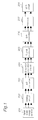
- Fig. 1 shows a block diagram of a camcorder including a gradation correction device 204 of a first embodiment of the present invention.
- R, G and B signals as input picture signals detected by a solid state image sensor 201 such as a charge coupled device (CCD) is supplied through an analog circuit 202 to an analog-to-digital converter 203.
- the converter 203 converts the R, G and B signals to digital data of 0 - 255 level to be supplied to the gradation correction device 204.
- a gradation correction characteristic most appropriate to the input picture signals is determined and gradation correction is performed according thereto.
- a gradation correction characteristic is referred hereinafter to a relation of output signal against input signal, as shown in Fig. 5.
- a signal processor 205 performs signal processing such as aperture processing.
- the processed digital R, G and B signals are converted to analog R, G and B signals by a digital-to-analog converter 206.
- an encoder 207 converts the analog R, G and B signals to Y signal (luminance signal) and C signals (color signals) and a VCR circuit 208 records them in a video tape.
- Fig. 2 shows an example of a 1-frame picture of input picture signals in a frame plane 501.
- This picture shows a person standing in front of a window. Due to strong back-light , the person becomes very dark while a landscape which can be seen through the window becomes very bright.
- the number of samples in the frame plane 501 is 640 points along a horizontal direction and 480 points along a vertical direction.
- Fig. 3 shows effective pixels in the frame plane 501, wherein effective pixels are represented as open circles (O).
- the effective pixels selected consists of every other pixel in the horizontal direction and every other line in a central region of 512 pixels in the horizontal direction and 400 lines along a vertical lines. Therefore, the number of samples in the effective area is 256 points along the horizontal direction and 200 points along the vertical direction.
- the effective area consists of 256 points times 200 points.
- the area size or point number of signals for expressing the number of pixels may be selected to be any number large enough to extract features of an input picture, and feature quantities can be extracted by counting the frequencies of pixels in different level ranges in the effective area in a histogram.
- the bit number of feature quantities or frequencies of pixels may also be any number large enough to express features of a picture.
- Fig. 4 shows a block diagram of the gradation correction device 204.
- a known matrix circuit 101 receives input picture signals and provides luminance signal Y to a feature quantity extraction circuit 102 and to a correction gain generation circuit 104.
- the feature quantity extraction circuit 102 extracts feature quantities from the luminance signals Y in the above-mentioned effective area.
- the feature quantities which are used to determine gradation correction characteristic are defined to represent the kind of a picture.
- the feature quantities represent level distribution of the luminance signals Y in the effective pixels of 256 * 200 dots.
- a correction coefficient determination circuit 103 determines a gradation correction characteristic appropriate for the input digital picture signals of the picture according to the extracted feature quantities.
- the correction coefficient determination circuit 103 determines a correction coefficient characterizing the appropriate gradation correction characteristic and the correction coefficient is used to correct the input picture signals. Then, input digital picture signals are corrected according to the appropriate gradation correction characteristic. That is, first, the correction gain generation circuit 104 receives the luminance signal Y and the correction coefficient received from the correction coefficient determination circuit 103 and sends a correction gain (Y'/Y) to a correction circuit 105.
- the correction circuit 105 adjusts the timing of the R, G and B signals with the correction gain by delays 106 by a delay time for calculating the gradation correction characteristic, and it multiplies them with the correction gain (Y'/Y) by the multipliers 107 to supply R', G' and B' signals after gradation correction to the signal processor 205.
- the delays 106 are used for timing control in the circuit 105, 1-field or 1-frame memories may be used instead of the delays 106. In such a case, a same picture is read twice.
- it is a characteristic of the gradation correction device 204 that it processes digital data.
- it is relatively easy to change gradation characteristic according to the features of various kinds of a picture.
- gradation correction characteristic is determined automatically according to feature quantities extracted from input digital picture signals.
- the gradation correction characteristic represents a relation of output level against input level of picture signals.
- Fig. 5 shows gradation correction characteristic in the present embodiment, wherein reference sign Y1 denotes a first gradation correction characteristic and reference sign Y2 denotes a second gradation correction characteristic.
- a corrected value of input picture signal can easily be obtained, as will be explained later, by using the gradation correction coefficient which characterizes an interpolation characteristic between the two Y1 and Y2. Therefore, an output picture of good color balance and rich gradation expression can be supplied for all objects from a back-lit object to a front-lit object without deteriorating gradation.
- the gradation correction device 204 is explained in detail below.
- the matrix circuit 101 calculates luminance signal Y from R, G and B signals.
- the luminance Y ranges also between 0 and 255.
- the luminance Y is supplied to the feature quantity extraction circuit 102 and to the correction gain generation circuit 103.
- Fig. 6 shows the feature quantity extraction circuit 102 for extracting feature quantities from the luminance signals Y of a picture.
- frequencies of luminance signal at three sections of low, middle and high luminances are counted over an effective area in a 1-frame picture, and the frequencies are used as feature quantities.
- the input luminance signal Y is compared with first and second threshold values by a comparator 701. If the luminance signal Y is smaller than the first threshold value, a count signal for low luminance section is supplied to a first counter 702. If the luminance signal Y is between the first and second threshold values, a count signal for middle luminance section is supplied to a second counter 703. If the luminance signal is larger than the second threshold value, a count signal for high luminance section is supplied to a third counter 704.
- the counters 702, 703 and 704 provide the frequencies of low, middle and high luminance sections for an effective area.
- Fig. 7 shows an example of a histogram of luminance obtained by the feature quantity extraction circuit 102.
- a histogram "a” obtained by counting frequencies at each luminance level is illustrated for comparison.
- Reference signs "b", "c” and “d” denote frequencies of pixels of low luminance section from 0 to 63, of middle luminance section from 64 to 191 and of high luminance section from 192 to 255, respectively.
- the histogram shown in Fig. 7 has two peaks at low and high luminance sections larger than the number at middle luminance section. Therefore, it is guessed that this picture is taken for a back-lit object.
- the feature quantity extraction circuit 102 provides frequencies of pixels for three luminance levels.
- the two threshold values for determining sections for extraction can be changed suitably.
- the number of luminance level sections may also be different from three.
- Fig. 8 shows a correction coefficient determination circuit 103.
- a correction coefficient table ROM 801 stores correction coefficients for a front-lit object, for a back-lit object, for a dark object and the like while receiving frequencies of pixels of low, middle and high luminance sections as input signals. Therefore, when the three frequencies of pixels of low, middle and high luminance sections are received by the correction coefficient table ROM 801 from the feature quantity extraction circuit 102, a correction coefficient is determined for gradation correction of an input picture.
- the correction coefficient is filtered by the filter 802 so as to keep gradation continuity of moving pictures with respect to previous frames, as will be explained later.
- Fig. 9 shows an internal structure of an example of the correction coefficient table ROM 801 including an M-L calculator 13, a first quantization memory 14, a second quantization memory 15, a decision memory 16 and a bit shift circuit 42 for shifting 6-bit data to the left.
- the M-L calculator 13 receives 16-bit data of the frequencies of pixels of low, middle and high luminance sections and generates values L, M and H as most significant 8-bit data of the 16-bit data. It also calculates (100 + M/4 - L/2). Then, it provides 8-bit data of (100 + M/4 - L/2) and of H to the quantization memories 14 and 15 as addresses.
- Fig. 10 shows an example of the contents of the quantization memories 14 and 15.
- the first quantization memory 14 provides "0" if 0 ⁇ (100 + M/4 - L/2) ⁇ 5.
- the level width of middle luminance section is double that of low luminance range.
- the value "100" is a constant added for convenience.
- the memories 14 and 15 provide quantization values of a 4-bit data and of a 3-bit data, respectively.
- the capacity of the first quantization memory 14 is 128 bytes (or 256 words times 4 bits), while that of the second one 15 is 96 bytes (or 256 words times 3 bits).
- Fig. 11 shows the content of the decision memory 16.
- the decision memory 16 receives the 4-bit quantization value from the first quantization memory 14 and the 3-bit quantization value from the second one 15 as a 7-bit address signal, and it provides a 5-bit parameter ( ⁇ ) in correspondence to the address. For example, if "0" is received from the first quantization memory 14 and "0" is also received from the second one 15, the decision memory 16 provides "-4.0". It is shown that an output value increases from -4.0 to +4.0 from a back-lit object (M/4 ⁇ L/2) to a front-lit object (M/4 > L/2). It is also shown that an output value increases with increasing H.
- the capacity of the decision memory 16 is 80 bytes (or 128 words times 5 bits).
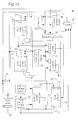
- Fig. 12 shows a circuit diagram of the filter 802 in detail.
- a synchronous pulse generator 37 generates pulse signals (VD) and master clock signals (f ck ), both having rising edges in synchronization with the start of a frame.
- reference numeral 18 denotes a comparator
- reference numerals 21, 22 and 23 denote inverters
- reference numerals 23, 25 and 34 denote AND gates.
- a subtractor 30 receives a 5-bit parameter ⁇ from the correction coefficient table ROM 801 and the correction coefficient ( ⁇ ) for the previous frame held in a correction gamma register 17 and calculates a difference ( ⁇ - ⁇ ).
- a shift bit number counter 32 counts master clock signals, and a shift bit number comparator 33 compares the count of the counter 32 with a number set in a shift bit number register 31 and supplied shift clocks to a shift register 35.
- the shift register 35 shifts the difference ( ⁇ - ⁇ ) to right by a bit number set in the shift bit number register 31.
- An adder 36 adds the ⁇ of the previous frame with the shifted difference ( ⁇ - ⁇ ) and supplies a sum to the correction gamma register 17 to update the correction coefficient for each frame.
- a plus frame number counter 19 counts a number of frames which has ⁇ larger than ⁇ continuously
- a minus frame number counter 20 counts a number of frames which has ⁇ smaller than ⁇ continuously.
- a plus frame number comparator 27 and a minus frame number comparator 28 compare the counts in the plus and minus frame number counters 19 and 20 with the inoperative frame number set previously in a register 26, respectively. If the number set in the inoperative frame number register 26 is smaller than the values set in the plus and minus frame number counters 19 and 20, the shift register 35 is cleared according to a pulse signal received from a NAND gate 29, and the adder 36 provides the same correction coefficient as that of the previous frame. Thus, the correction coefficient does not change until frames of ⁇ > ⁇ or ⁇ ⁇ ⁇ continue by more than the inoperative frame number.
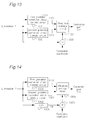
- Fig. 13 shows a block diagram of the gradation correction gain generation circuit 104 of the first embodiment including a first gradation correction characteristic circuit 301, a second gradation correction characteristic circuit 302, an adder 303 and a weighted average circuit 304.
- An input luminance signal Y is supplied to the first and second gradation correction characteristic circuits 301 and 302.
- a first correction gain (Y1/Y) is sent according to the input luminance signal Y and Y1 obtained from a first gradation correction characteristic.
- a second correction gain (Y2/Y) is sent according to the input luminance signal Y and Y2 obtained from a second gradation correction characteristic.
- the first correction gain (Y1/Y) follows Equation (4) while the second correction gain (Y2/Y) follows Equation (5).
- (Y1/Y) ⁇ 1/255 2 *(Y-255) 3 + 255 ⁇ /Y.
- (Y2/Y) Y/Y.
- Fig. 5 shows gradation correction characteristics used in the present embodiment, wherein Y1 and Y2 denote the first and second gradation correction characteristics, respectively.
- the gradation correction characteristic is represented as "a”. If the correction coefficient is positive, the gradation correction characteristic decreases below the characteristic "a", as illustrated for example as "c”. If the correction coefficient is negative, the gradation correction characteristic increases above the characteristic "a", as illustrated for example as "b".
- the gradation correction characteristic can easily be changed gradually and continuously. By decreasing the correction coefficient, the correction gain at low and middle luminances increases gradually, and finally it is enhanced in the entire range.
- every object can be corrected to express rich gradation by using for example the gradation correction characteristic "Y2" for a front-lit object, the gradation correction characteristic "a” for a back-lit object and the gradation correction characteristic "Y1" for a dark object.
- the correction gain generation circuit 104 generates the correction gain for an input picture signal by using the correction coefficient, and the correction gain is used in the correction circuit 105 to correct the input picture signal by multiplying it with the correction gain. It is to be noted on the correction gain generation circuit 104 that it does not need ROMs or the like to store a plurality of kinds of gradation correction characteristics, and the scale of the circuit can be made very compact. Still further, because a gradation correction characteristic can be generated for front-lit and back-lit objects by changing the correction coefficient, an output picture of good color balance and rich gradation expression can be obtained for all objects from back-lit object to front-lit object without deteriorating gradation.
- the gradation correction characteristic can be changed gradually and continuously, gradation correction can be performed naturally even for a moving picture. Still further, the contrast at high luminance is preserved by the gradation correction characteristic "a" in Fig. 5 for back-lit object. On the other hand, in a prior art so-called auto-knee control, the gradation at high luminance is deteriorated.
- a second embodiment of the gradation correction device 204 is explained. It is similar to the first embodiment except the correction gain generation circuit 104'.
- Fig. 14 shows a block diagram of the gradation correction gain generation circuit 104' of this embodiment This circuit is different from that of the first example shown in Fig. 13 in that an average detection circuit (low pass filter) 1305 is provided newly to generate a weight.
- An input luminance signal Y is supplied to first and second gradation correction characteristic circuits 1301 and 1302.
- a first correction gain (Y1/Y) is sent according to the input luminance signal Y.
- a second correction gain (Y2/Y) is sent according to the input luminance signal Y.
- the average detection circuit (LPF) 1305 obtains an average luminance Ya from luminance signals Y. That is, it averages luminance signals of say three or five pixels around a pixel of interest.
- a weighted average circuit 1304 averages the first and second correction gains with a weight determined according to Equation (2') by using the signal X and supplies a correction gain (Y'/Y) to the correction circuit 105.
- Fig. 15 illustrates gradation correction characteristics and input/output characteristic in an example.
- output picture signals show edge emphasis.
- the average luminance Ya obtained by the average detection circuit (LPF) 1305 is equal to a luminance signal Y of a pixel of interest
- the gradation characteristic "a" shown in Fig. 15 is adopted.
- the average luminance Ya is smaller than a luminance signal Y of a pixel of interest
- the gradation characteristic "b” shown in Fig. 15 is adopted.
- the average luminance Ya is larger than a luminance signal Y of a pixel of interest
- the gradation characteristic "c" shown in Fig. 15 is adopted.
- the gradation correction characteristic can be changed for each pixel appropriately. Even if a gradation correction characteristic curve has a small slope, the contrast of an output picture is good, and output signals can express gradation richly.
- Fig. 16 shows a block diagram of an example of the gradation correction gain generation circuit 104'.
- the circuit calculates Equations (2'), (3), (4) and (5).
- the circuit is simplified by using bit shift for multiplication or division of 255 and the like.
- a luminance signal Y is received, an average Ya is obtained by an average detection circuit (low pass filter) 401.
- a first adder 402 adds the average luminance Ya with the correction coefficient.
- a clip circuit 403 clips an output signal of the first adder with a value "0" for smaller values and with a value "255" for larger values.
- the luminous signal Y is delayed via a delay 400 for synchronization and a signal 2Y obtained by one-bit shift of Y are received by a second adder 404, and a signal 2Y is added with Y to send a signal 3Y of three times Y.
- a first multiplier 405 multiplies the luminance signal Y twice to generate a luminance signal Y 2 .
- a third adder 406 adds the output of the first multiplier 405 with a value "3".
- a first subtractor 407 subtracts the output signal "Y 2 + 3" of the third adder 406 with "3Y" of the second adder 404.
- the first gradation correction characteristic circuit 1301 of this example consists of the second adder 404, the first multiplier 405, the third adder 406 and the first subtractor 407. Then, the second subtractor 409 subtracts the output signal of the clip circuit 403 from "255". Then, a second multiplier 408 multiplies the output signal of a second subtractor 409 with that of the first subtractor 407. Finally, a fourth adder 410 adds the output signal of the clip circuit 403 with that of the second multiplier 408 to send a product as a correction gain.
- the weighted average circuit 1404 consists of the second multiplier 408, the second subtractor 409 and the fourth adder 410.
- the correction gain is controlled according the correction coefficient with use of the gradation correction characteristics shown in Figs. 5 and 15. Because a gradation correction characteristic can be generated for every object by changing the correction coefficient, an output picture of good color balance and rich gradation expression can be obtained for all objects from back-lit objects to front-lit objects without deteriorating gradation.
- the average detection circuit 1305 averages input luminance signals including an input luminance signal of interest and input luminance signals thereabout. In other words, the circuit 1305 outputs an average of luminance signals around the input luminance signal of interest. Therefore, the luminance is corrected smaller or larger if the average luminance is larger or smaller. Therefore, even the gradation correction keeps contrast even if the slope of the gradation correction characteristic is small and output signals of rich gradation expression can be obtained.
- the above-mentioned correction gain generation circuit 104' generates the correction gain by using the correction coefficient without ROMs and the like to store a plurality of kinds of gradation correction characteristics. Therefore, the scale of the circuit can be made very compact. Still further, the contrast at high luminance is preserved for a back-lit object. On the other hand, in a prior art so-called auto-knee control, the gradation at high luminance is deteriorated. Further, gradation correction is performed in the unit of pixel by changing the gradation correction characteristic suitably according to the average luminance Ya. Therefore, the gradation correction keeps contrast even if the slope of the gradation correction characteristic is small, and output signals of rich gradation expression can be obtained.
- Fig. 17 shows a block diagram of an image sensing device which can correct gradation according to a third embodiment of the present invention.
- This device is similar to that of the first embodiment shown in Fig. 1 except that feature extraction and correction determination are carried out by using a software program.
- R, G and B signals as input picture signals are sensed by a solid state image sensor 1101 through an analog circuit 1102.
- the R, G and B signals are converted by an analog-to-digital converter 1103 to digital data of 0 - 255, which are supplied as input picture signals to a matrix circuit 1104 and to the gradation correction means 1108.
- a matrix circuit 1104 calculates a luminance signal Y from the digital R, G and B signals, and it supplies the luminance signal Y to a feature quantity extraction means 1105 for extracting feature quantities and to a correction gain generation means 1107 for generating a correction gain.
- the feature quantity extraction means 1105 extracts features of pixels of low, middle and high luminance sections of the luminance signal Y and supplies them as feature quantities to a correction coefficient determination means 1106.
- This means 1106 decides a gradation correction characteristic most appropriate to the input picture signal and sends a gradation correction coefficient characterizing the gradation correction characteristic.
- a correction gain generation means 1107 outputs a correction gain according to the luminance signal Y and the correction coefficient, and a gradation correction means 1108 multiplies the input picture signals with the correction gain for gradation correction.
- the signal processor 1109 performs signal processing such as aperture processing.
- the processed digital R, G and B signals are converted to analog R, G and B signals by a digital-to-analog converter 1110.
- an encoder 1111 converts the R, G and B signals to Y signal (luminance signal) and C signal (C signal).
- a VCR circuit 1112 records them in a video tape.
- Fig. 18 shows a block diagram of an image sensing device of an example according to a third embodiment of the present invention, wherein a solid state image sensor 1201, an analog circuit 1202, an analog-to-digital (A/D) converter 1203, a gradation correction circuit 1204, a signal processor 1205, a digital-to-analog (D/A) converter 1206, an encoder 1207 and a VCR circuit 1208 are similar to the counterparts shown in Fig. 17.
- A/D analog-to-digital
- D/A digital-to-analog
- the R, G and B signals are converted by the analog-to-digital converter 1203 to digital data of 0 - 255 level, which are supplied as input picture signals to a histogram generation means 1209 and to a gradation correction means 1204.
- the histogram generation means 1209 calculates a luminance signal Y from the R, G and B signals to generates frequencies of pixels of low, middle and high luminance sections for a 1-frame of an effective picture plane to extract feature quantities.
- a microprocessor 1212 is connected via a bus 1215 to a ROM 1213, a RAM 1214, an input means 1210 such as a key board and a correction gain generation circuit 1211.
- the ROM 1213 stores templates which includes features of gradation correction characteristic, while the RAM 1214 stores the numbers of pixels of low, middle and high luminances received from the histogram generation means 1209.
- the microprocessor 1212 determines a correction coefficient according to a flowchart shown in Fig. 19.
- the microprocessor 1212 determines the gradation correction characteristic by using template matching with reference to Fig. 19.
- the frequencies of pixels of low, middle and high luminance sections are read from the histogram generation means 1209 and stored in the RAM 1214 (step S10).
- the distances of the numbers stored in the RAM 1214 from templates stored in the ROM 1213 are calculated (step S12).
- the templates represent gradation correction characteristics to be selected according to feature quantities of input picture signals.
- a gradation correction characteristic of the shortest distance is determined (step S14).
- a processing is performed for keeping gradation continuity with the gradation correction characteristic of a previous field.
- a correction coefficient is sent for the correction gain generation circuit 1211 (step S16).
- the correction gain generation circuit 1211 averages the first and second gradation correction characteristics with a weight according to a sum of the average of the input luminance signal and the correction coefficient and supplies a correction gain to the gradation correction circuit 1204.
- the circuit 1204 adjusts the timing of the R, G and B signals according to the correction gain, and multiplies each of the R, G and B signals with the correction gain to send corrected R, G and B signals after gradation correction.
- the signal processor 1205 performs signal processing such as aperture processing.
- the processed digital R, G and B signals are converted to analog R, G and B signals by the digital-to-analog converter 1206.
- the encoder 1207 converts the R, G and B signals to Y signal (luminance signal) and C signal (C signal).
- the VCR circuit 1208 records them in a video tape.
- the image sensing device can provide an output picture of good color balance and rich gradation expression for all objects from back-lit object to front-lit object without deteriorating gradation. Still further, the contrast at high luminance is preserved for a back-lit object.
- the gradation at high luminance is deteriorated.
- gradation correction is performed in the unit of pixel by changing the gradation correction characteristic according to the average luminance Ya. Then, the gradation correction keeps contrast even if the slope of the correction gain is small, and output signals of rich gradation expression can be obtained.
- a natural picture can be provided with use of gradation correction.
- Fig. 20 shows a block diagram of a gradation correction device according to a fourth embodiment of the present invention.
- the gradation correction device includes a feature quantity extraction circuit 1401, a correction coefficient determination circuit 1402, a correction gain generation circuit 1403, a correction circuit 1404, delays 1405 and multipliers 1406.
- This gradation correction device is different from that shown in Fig. 4 in that a matrix circuit is omitted because input picture signal includes luminance and color signals.
- a luminance signal Y and color difference signals R-Y, B-Y are received by the gradation correction device. Therefore, a matrix circuit for calculating luminous signal can be omitted because the luminance signal Y is received.
- the functions of a feature quantity extraction circuit 1401, a correction coefficient determination circuit 1402, a correction gain generation circuit 1403 and a gradation correction means 1404 are similar to the counterparts in the first embodiment. That is, the luminance signal Y to the feature quantity extraction circuit 1401 and to the correction gain generation circuit 1403.
- the feature quantity extraction circuit 1401 extracts features of pixels of low, middle and high luminance sections of the luminance signal Y and supplies them to the correction coefficient determination circuit 1402.
- the circuit 1402 decides a gradation correction characteristic most appropriate to the input picture signals and sends a correction coefficient to the gradation gain generation circuit 1403.
- the circuit 1403 outputs a correction gain according to the luminance signal Y and the correction coefficient to the correction circuit 1404.
- the delay circuits 1405 adjust the timings of input picture signals and the multipliers 1406 multiply the picture signals with the correction gain to send corrected luminance signal Y' and color difference signals (R-Y)' and (B-Y)'.
- an output picture of good color balance and rich gradation expression can be obtained for all objects from back-lit object to front-lit object without deteriorating gradation.
- R, G and B signals or luminance signal and color difference signals are used as input digital picture signals.
- other signals which vary with luminance can also be used as input digital picture signals.
- Such signals include a composite signal or a signal synthesized from the luminance and color signals.
- the correction circuit multiplies each of input picture signals with the correction gain.
- a correction value (Y-Y') is calculated and gradation is corrected by adding the correction value (Y-Y') to each of the input picture signals, instead of the above-mentioned multiplication with the correction gain (Y'/Y).
- a correction difference circuit is provided to calculate (Y-Y') instead of the correction gain circuit 104 and adders are used for the addition of (Y-Y') instead of the multipliers 107 provided in the correction circuit 105.
- an input picture signal is converted to an 8-bit digital signal.
- the bit number for quantization may be a number different from eight.
- the bit number to be processed in the correction gain generation circuit and the like can be adjusted according to the bit number for quantization.
- a gradation correction device is provided for gradation correction in a camcorder. Therefore, gradation correction device receives input picture signals from the solid state image sensor 201 through the analog circuit 202.
- a different recording medium can also be used to provide input picture signals: for example, a laser disc, a video tape, a magnetic disc or the like for analog picture recording and a magnetic disc such as a hard disc or an optical disc for a digital recording after analog-to-digital conversion.
- input recording signals are supplied from such a recording medium.
- the gradation correction device of the invention can be applied to any recording medium which stores a 1-frame or a 1-field picture data, wherein the solid state image sensor 201 and the analog circuit 202 can be replaced with an appropriate device.
- the correction coefficient determination circuit decides the correction coefficient of input picture signals according to a luminance histogram.
- other feature quantities which can classify a picture or which reflect luminance level distribution may be used instead of the luminance histogram.
- each histogram of red (R), green (G) and blue(B) signals, or one of them (say green (G)) can used.
- the correction coefficient determination circuit can use any process for determining an appropriate gradation correction characteristic from input picture signals.
- a neural network or fuzzy control can be used to determine appropriate gradation correction characteristic besides the above-mentioned template matching.
- a gradation correction circuit according to the present invention and of an image sensing device therewith that it can determine a most suitable gradation correction characteristic automatically by deciding a picture according to feature quantities obtained from input picture signals.
- extreme black or white can be prevented in a reproduced picture, and an output picture of good color balance and rich gradation expression can be obtained for all objects from back-lit object to front-lit object without deteriorating gradation.
Claims (19)
- Dispositif de correction de gradation comprenant :un moyen d'extraction de quantités de détails (102) pour extraire des quantités de détails à partir de signaux d'image numériques en entrée d'une image, lesquelles quantités de détails reflètent la distribution des niveaux de luminance des signaux d'image numériques en entrée ;un moyen de détermination de coefficient de correction de gradation (103) pour déterminer un coefficient de correction de gradation basé sur les quantités de détails reçues du moyen d'extraction de quantités de détails (102) ;un moyen de génération de facteur de correction (104) qui génère un facteur de correction (Y/Y') sur la base du niveau de luminance (Y) et du coefficient de correction de gradation en conformité avec un niveau du signal du signal de luminance ; etun moyen de correction de gradation (105) qui traite le signal d'image numérique en entrée avec le facteur de correction généré par ledit moyen de génération de facteur de correction (104) ;d'où il résulte que le coefficient de correction de gradation concernant les signaux numériques d'image en entrée est varié conformément à ces détails.
- Dispositif de correction de gradation selon la revendication 1, dans lequel lesdits signaux d'image en entrée comprennent un signal de luminance et des signaux de différences de couleurs.
- Dispositif de correction de gradation selon la revendication 1, comprenant de plus un moyen de génération de signal de luminance pour séparer ou synthétiser le signal de luminance à partir des signaux d'image numériques en entrée.
- Dispositif de correction de gradation selon la revendication 3, dans lequel ledit moyen de génération de signal de luminance comprend un circuit matriciel (101) pour générer le signal de luminance à partir des signaux R, V et B.
- Dispositif de correction de gradation selon la revendication 1, dans lequel ledit moyen d'extraction de quantités de détails (102) détermine la disposition des niveaux de luminance en calculant un histogramme des signaux de luminance de l'image, les signaux de luminance étant classés en une pluralité de sections, les valeurs des fréquences des sections étant utilisées comme lesdites quantités de détails.
- Dispositif de correction de gradation selon la revendication 5, dans lequel le nombre desdites sections est de trois.
- Dispositif de correction de gradation selon la revendication 1, dans lequel ledit moyen de détermination de coefficient de correction de gradation (103) détermine le coefficient de correction de gradation en mettant en moyenne deux coefficients de correction de gradation prescrits avec un poids déterminé en conformité avec les quantités de détails reçues à partir dudit moyen d'extraction de quantités de détails (102).
- Dispositif de correction de gradation selon la revendication 1, dans lequel ledit moyen de détermination de coefficient de correction de gradation (103) comprend :un moyen de quantification servant à quantifier les quantités de détails reçues dudit moyen d'extraction de quantités de détails ; etun moyen de table (801) pour délivrer un coefficient de correction pour déterminer la caractéristique de correction de gradation en conformité avec les valeurs quantifiées quantifiées par le moyen de quantification.
- Circuit de correction de gradation selon la revendication 8, dans lequel ledit moyen de détermination de coefficient de correction (103) comprend de plus :un moyen de mémoire pour mémoriser un coefficient de correction d'une image précédente ;un moyen de comptage pour compter un nombre d'images successives où le coefficient de correction reçu à partir dudit moyen de table est successivement plus grand ou successivement plus petit que le coefficient de correction mémorisé dans le moyen de mémoire ; etun moyen de mise à jour pour déterminer le coefficient de correction qui doit être délivré audit moyen de correction en conformité avec le nombre d'images successives reçu dudit moyen de comptage.
- Circuit de correction de gradation selon la revendication 8, dans lequel ledit moyen de détermination de coefficient de correction (103) comprend de plus :un moyen de mémoire pour mémoriser un coefficient de correction d'une image précédente ; etun moyen de mise à jour pour déterminer le coefficient de correction qui doit être délivré audit moyen de correction en conformité avec une différence du coefficient de correction reçu à partir dudit moyen de table avec le coefficient de correction mémorisé dans le moyen de mémoire.
- Dispositif de correction de gradation selon la revendication 1, dans lequel ledit moyen de génération de facteur de correction (104) génère un gain de correction pour les signaux d'image numériques en entrée comme le facteur de correction en conformité avec les signaux d'image numériques en entrée et le coefficient de correction déterminé par ledit moyen de détermination de caractéristique de correction de gradation ; et
ledit moyen de correction de gradation (105) multiplie les signaux d'image numériques en entrée par le gain de correction reçu du moyen de génération de facteur de correction (104). - Dispositif de correction de gradation selon la revendication 1, dans lequel ledit moyen de génération de facteur de correction (104) comprend :un premier moyen (301) pour générer une première valeur de sortie d'une première caractéristique de correction de gradation pour un signal d'image numérique en entrée ;un second moyen (302) pour générer une seconde valeur de sortie d'une seconde caractéristique de correction de gradation pour le signal d'image numérique en entrée ;un moyen d'additionneur (303) pour additionner le signal d'image numérique en entrée et le coefficient de correction déterminé par ledit moyen de détermination de coefficient de correction de gradation (103) pour délivrer un poids ; etun moyen de moyenne pondérée (304) pour déterminer le gain de correction en mettant en moyenne les première et seconde valeurs de sortie avec le poids.
- Dispositif de correction de gradation selon la revendication 1, dans lequel ledit moyen de génération de facteur de correction (104) comprend :un premier moyen pour générer une valeur de sortie d'une première caractéristique de correction de gradation pour un signal d'image numérique en entrée ;un second moyen pour générer une valeur de sortie d'une seconde caractéristique de correction de gradation pour le signal d'image numérique en entrée ;un moyen de mise en moyenne pour obtenir une moyenne des signaux d'image numériques en entrée incluant le signal d'image numérique en entrée et les signaux autour de celui-ci ;un moyen d'additionneur pour additionner la moyenne reçue du moyen de mise en moyenne et le coefficient de correction déterminé par ledit moyen de détermination de caractéristique de correction de gradation pour délivrer un poids ; etun moyen de moyenne pondérée pour déterminer le gain de correction en mettant en moyenne les deux valeurs de sortie avec le poids.
- Circuit de correction de gradation selon la revendication 12, dans lequel ladite première caractéristique de gradation Y1 du signal d'image en entrée Y change en conformité avec une équation suivante :
- Circuit de correction de gradation selon la revendication 13, dans lequel ladite première caractéristique de gradation Y change avec le signal d'image en entrée Y en conformité avec une équation suivante :
- Circuit de correction de gradation selon la revendication 1, ledit moyen de génération de facteur de correction comprend :un circuit de détection de moyenne pour obtenir une moyenne Ya d'un signal d'image en entrée Y et des signaux d'image numériques en entrée autour de celui-ci ;un premier additionneur pour additionner la moyenne Ya avec ledit coefficient de correction ;un circuit d'écrêtage pour écrêter un signal de sortie du premier additionneur à une valeur de "0" et un niveau maximal du signal d'image en entrée Y ;un second additionneur pour additionner le signal d'image en entrée Y afin de délivrer 3Y ;un premier multiplicateur pour multiplier le signal d'image en entrée Y deux fois afin de délivrer Y2 ;un troisième additionneur pour additionner un signal de sortie du premier multiplicateur avec une constante ;un premier soustracteur pour soustraire un signal de sortie du second additionneur d'un signal de sortie du troisième additionneur ;un second soustracteur pour soustraire un signal de sortie du circuit d'écrêtage du niveau maximal du signal d'image en entrée ;un second multiplicateur pour multiplier un signal de sortie du premier soustracteur par un signal de sortie du second soustracteur ; etun quatrième additionneur pour additionner un signal de sortie du circuit d'écrêtage avec un signal de sortie du second multiplicateur pour délivrer le gain de correction.
- Dispositif de correction de gradation selon la revendication 1, dans lequel ledit moyen de génération de facteur de correction comprend :un moyen de génération de différence de correction génère une différence de correction d'un signal corrigé à partir des signaux d'image numériques en entrée comme le facteur de correction, lequel signal corrigé est calculé en conformité avec les signaux d'image numériques en entrée et avec le coefficient de correction déterminé par ledit moyen de détermination de coefficient de correction de gradation (103) ; etledit moyen de correction de gradation (105) additionne les signaux d'image numériques en entrée avec la différence de correction reçue du moyen de génération de différence de correction.
- Dispositif de détection d'image comprenant :un moyen de capteur d'image (1101 à 1103) pour détecter les signaux d'image en entrée d'une image pour délivrer des signaux d'image numériques en entrée ;un moyen d'extraction de quantités de détails (1105) pour extraire des quantités de détails à partir des signaux d'image numériques en entrée d'une image, lesquelles quantités de détails reflètent la distribution du niveau de luminance des signaux numériques d'image en entrée ;un moyen de détermination du coefficient de correction de gradation (1106) pour déterminer un coefficient de correction de gradation basé sur les quantités de détails (1105), lequel coefficient de correction de gradation définit un signal de sortie pour un signal d'entrée ;un moyen de génération de facteur de correction (1107) génère un facteur de correction sur la base du niveau de luminance et du coefficient de correction de gradation en conformité avec un niveau du signal du signal de luminance ; etun moyen de correction de gradation (1108) qui traite le signal d'image numérique en entrée avec le facteur de correction généré par ledit moyen de génération de facteur de correction (1107) ;d'où il résulte que le coefficient de correction de gradation pour les signaux numériques d'image en entrée varie en conformité avec ces détails.
- Dispositif de détection d'image selon la revendication 18, comprenant de plus un moyen pour enregistrer les signaux d'image corrigés de l'image sur un support d'enregistrement externe.
Applications Claiming Priority (4)
| Application Number | Priority Date | Filing Date | Title |
|---|---|---|---|
| JP03510593A JP3201049B2 (ja) | 1993-02-24 | 1993-02-24 | 階調補正回路及び撮像装置 |
| JP35105/93 | 1993-02-24 | ||
| JP133096/93 | 1993-06-03 | ||
| JP5133096A JPH06350875A (ja) | 1993-06-03 | 1993-06-03 | ビデオ信号の階調補正回路 |
Publications (2)
| Publication Number | Publication Date |
|---|---|
| EP0613294A1 EP0613294A1 (fr) | 1994-08-31 |
| EP0613294B1 true EP0613294B1 (fr) | 1998-10-28 |
Family
ID=26374025
Family Applications (1)
| Application Number | Title | Priority Date | Filing Date |
|---|---|---|---|
| EP94102684A Expired - Lifetime EP0613294B1 (fr) | 1993-02-24 | 1994-02-23 | Dispositif de correction de la gradation et dispositif capteur d'images equipé d'un tel dispositif |
Country Status (3)
| Country | Link |
|---|---|
| US (1) | US5517333A (fr) |
| EP (1) | EP0613294B1 (fr) |
| DE (1) | DE69414153T2 (fr) |
Cited By (11)
| Publication number | Priority date | Publication date | Assignee | Title |
|---|---|---|---|---|
| US8251820B2 (en) | 2003-09-15 | 2012-08-28 | Sony Computer Entertainment Inc. | Methods and systems for enabling depth and direction detection when interfacing with a computer program |
| US8303405B2 (en) | 2002-07-27 | 2012-11-06 | Sony Computer Entertainment America Llc | Controller for providing inputs to control execution of a program when inputs are combined |
| US8310656B2 (en) | 2006-09-28 | 2012-11-13 | Sony Computer Entertainment America Llc | Mapping movements of a hand-held controller to the two-dimensional image plane of a display screen |
| US8570378B2 (en) | 2002-07-27 | 2013-10-29 | Sony Computer Entertainment Inc. | Method and apparatus for tracking three-dimensional movements of an object using a depth sensing camera |
| US8675915B2 (en) | 2002-07-27 | 2014-03-18 | Sony Computer Entertainment America Llc | System for tracking user manipulations within an environment |
| US8781151B2 (en) | 2006-09-28 | 2014-07-15 | Sony Computer Entertainment Inc. | Object detection using video input combined with tilt angle information |
| US8947347B2 (en) | 2003-08-27 | 2015-02-03 | Sony Computer Entertainment Inc. | Controlling actions in a video game unit |
| US8976265B2 (en) | 2002-07-27 | 2015-03-10 | Sony Computer Entertainment Inc. | Apparatus for image and sound capture in a game environment |
| US9174119B2 (en) | 2002-07-27 | 2015-11-03 | Sony Computer Entertainement America, LLC | Controller for providing inputs to control execution of a program when inputs are combined |
| US9381424B2 (en) | 2002-07-27 | 2016-07-05 | Sony Interactive Entertainment America Llc | Scheme for translating movements of a hand-held controller into inputs for a system |
| US9393487B2 (en) | 2002-07-27 | 2016-07-19 | Sony Interactive Entertainment Inc. | Method for mapping movements of a hand-held controller to game commands |
Families Citing this family (82)
| Publication number | Priority date | Publication date | Assignee | Title |
|---|---|---|---|---|
| JP2748678B2 (ja) * | 1990-10-09 | 1998-05-13 | 松下電器産業株式会社 | 階調補正方法および階調補正装置 |
| DE4310727C2 (de) * | 1992-04-06 | 1996-07-11 | Hell Ag Linotype | Verfahren und Einrichtung zur Analyse von Bildvorlagen |
| EP0784399B1 (fr) * | 1994-09-30 | 2006-04-12 | Matsushita Electric Industrial Co., Ltd. | Dispositif de prise de vues |
| JP3444449B2 (ja) * | 1994-12-26 | 2003-09-08 | ソニー株式会社 | 映像信号処理装置 |
| EP0909515B1 (fr) * | 1997-03-06 | 2002-06-26 | Matsushita Electric Industrial Co., Ltd. | Appareil de correction du facteur de contraste |
| JP3113835B2 (ja) * | 1997-03-14 | 2000-12-04 | 松下電器産業株式会社 | 撮像装置 |
| JP2951909B2 (ja) * | 1997-03-17 | 1999-09-20 | 松下電器産業株式会社 | 撮像装置の階調補正装置及び階調補正方法 |
| JP2951910B2 (ja) * | 1997-03-18 | 1999-09-20 | 松下電器産業株式会社 | 撮像装置の階調補正装置及び階調補正方法 |
| EP0963111A1 (fr) | 1998-06-02 | 1999-12-08 | Deutsche Thomson-Brandt Gmbh | Méthode et appareil d'amélioration dynamique du contraste dans des images vidéo |
| EP1372340B1 (fr) * | 1998-06-02 | 2006-12-13 | Deutsche Thomson-Brandt Gmbh | Méthode et appareil d'amélioration dynamique du contraste dans des images vidéo |
| US7440612B2 (en) * | 1998-11-13 | 2008-10-21 | Sony Corporation | Image processing apparatus and method capable of correcting gradation of image data |
| JP4131348B2 (ja) * | 1998-11-18 | 2008-08-13 | ソニー株式会社 | 画像処理装置及び画像処理方法 |
| JP3208762B2 (ja) * | 1998-11-18 | 2001-09-17 | ソニー株式会社 | 画像処理装置及び画像処理方法 |
| US6453075B1 (en) | 1998-12-31 | 2002-09-17 | Eastman Kodak Company | Method for preserving image detail when adjusting the tone scale of a digital color image |
| US6275605B1 (en) * | 1999-01-18 | 2001-08-14 | Eastman Kodak Company | Method for adjusting the tone scale of a digital image |
| JP4356134B2 (ja) * | 1999-04-16 | 2009-11-04 | ソニー株式会社 | 画像処理装置及び画像処理方法 |
| JP3714657B2 (ja) * | 1999-05-12 | 2005-11-09 | パイオニア株式会社 | 階調補正装置 |
| WO2001022391A1 (fr) * | 1999-09-17 | 2001-03-29 | Matsushita Electric Industrial Co., Ltd. | Dispositif afficheur d'images |
| EP1235427A4 (fr) * | 1999-11-25 | 2006-01-11 | Matsushita Electric Ind Co Ltd | Procede et appareil de correction de gradation, et affichage video |
| US20020012126A1 (en) * | 1999-12-20 | 2002-01-31 | Hiroaki Nakamura | Image processing method and apparatus |
| US6721000B1 (en) | 2000-02-23 | 2004-04-13 | Neomagic Corp. | Adaptive pixel-level color enhancement for a digital camera |
| JP3757747B2 (ja) * | 2000-04-03 | 2006-03-22 | 株式会社ニコン | 電子カメラ、画像処理プログラムを記録した記録媒体、および画像処理方法 |
| EP1152604A1 (fr) * | 2000-04-24 | 2001-11-07 | Pulnix America, Inc. | Réduction de l'éblouissement vidéo |
| JP3938833B2 (ja) * | 2000-04-27 | 2007-06-27 | 株式会社リコー | 露出制御装置 |
| EP1164784A1 (fr) * | 2000-06-13 | 2001-12-19 | Koninklijke Philips Electronics N.V. | Prévention du phénomène de courbure |
| WO2002019695A1 (fr) * | 2000-08-29 | 2002-03-07 | Seiko Epson Corporation | Lecteur d'images |
| DE10064678C1 (de) * | 2000-12-22 | 2002-07-11 | Kappa Opto Electronics Gmbh | Verfahren zur Signalverbesserung in einer mit einer digitalen Farbvideokamera aufgenommenen Bilderfolge |
| JP2002232906A (ja) * | 2001-01-31 | 2002-08-16 | Ricoh Co Ltd | ホワイトバランス制御装置 |
| WO2003039137A1 (fr) * | 2001-11-01 | 2003-05-08 | Thomson Licensing S.A. | Procede d'amelioration du contraste dynamique |
| JP4550350B2 (ja) * | 2002-02-01 | 2010-09-22 | 株式会社ニコン | 電子カメラ |
| US7102669B2 (en) * | 2002-04-02 | 2006-09-05 | Freescale Semiconductor, Inc. | Digital color image pre-processing |
| JP4153715B2 (ja) * | 2002-04-08 | 2008-09-24 | 松下電器産業株式会社 | 映像信号処理装置及び映像信号処理方法 |
| KR100469391B1 (ko) * | 2002-05-10 | 2005-02-02 | 엘지전자 주식회사 | 메탈-인슐레이터-메탈 전계방출 디스플레이의 구동회로 및방법 |
| US7161579B2 (en) * | 2002-07-18 | 2007-01-09 | Sony Computer Entertainment Inc. | Hand-held computer interactive device |
| US7102615B2 (en) * | 2002-07-27 | 2006-09-05 | Sony Computer Entertainment Inc. | Man-machine interface using a deformable device |
| US7646372B2 (en) | 2003-09-15 | 2010-01-12 | Sony Computer Entertainment Inc. | Methods and systems for enabling direction detection when interfacing with a computer program |
| US8797260B2 (en) | 2002-07-27 | 2014-08-05 | Sony Computer Entertainment Inc. | Inertially trackable hand-held controller |
| US7623115B2 (en) * | 2002-07-27 | 2009-11-24 | Sony Computer Entertainment Inc. | Method and apparatus for light input device |
| US9474968B2 (en) | 2002-07-27 | 2016-10-25 | Sony Interactive Entertainment America Llc | Method and system for applying gearing effects to visual tracking |
| US7803050B2 (en) | 2002-07-27 | 2010-09-28 | Sony Computer Entertainment Inc. | Tracking device with sound emitter for use in obtaining information for controlling game program execution |
| US8160269B2 (en) | 2003-08-27 | 2012-04-17 | Sony Computer Entertainment Inc. | Methods and apparatuses for adjusting a listening area for capturing sounds |
| US7918733B2 (en) | 2002-07-27 | 2011-04-05 | Sony Computer Entertainment America Inc. | Multi-input game control mixer |
| US8233642B2 (en) | 2003-08-27 | 2012-07-31 | Sony Computer Entertainment Inc. | Methods and apparatuses for capturing an audio signal based on a location of the signal |
| US8686939B2 (en) | 2002-07-27 | 2014-04-01 | Sony Computer Entertainment Inc. | System, method, and apparatus for three-dimensional input control |
| US7627139B2 (en) * | 2002-07-27 | 2009-12-01 | Sony Computer Entertainment Inc. | Computer image and audio processing of intensity and input devices for interfacing with a computer program |
| US8139793B2 (en) | 2003-08-27 | 2012-03-20 | Sony Computer Entertainment Inc. | Methods and apparatus for capturing audio signals based on a visual image |
| US9682319B2 (en) | 2002-07-31 | 2017-06-20 | Sony Interactive Entertainment Inc. | Combiner method for altering game gearing |
| EP1494462A4 (fr) * | 2003-01-09 | 2005-10-26 | Sony Corp | Dispositif et procede de traitement d'images |
| US9177387B2 (en) | 2003-02-11 | 2015-11-03 | Sony Computer Entertainment Inc. | Method and apparatus for real time motion capture |
| US8072470B2 (en) | 2003-05-29 | 2011-12-06 | Sony Computer Entertainment Inc. | System and method for providing a real-time three-dimensional interactive environment |
| US10279254B2 (en) * | 2005-10-26 | 2019-05-07 | Sony Interactive Entertainment Inc. | Controller having visually trackable object for interfacing with a gaming system |
| US8323106B2 (en) | 2008-05-30 | 2012-12-04 | Sony Computer Entertainment America Llc | Determination of controller three-dimensional location using image analysis and ultrasonic communication |
| US7663689B2 (en) * | 2004-01-16 | 2010-02-16 | Sony Computer Entertainment Inc. | Method and apparatus for optimizing capture device settings through depth information |
| JP4078649B2 (ja) * | 2004-01-28 | 2008-04-23 | 日本ビクター株式会社 | 映像信号処理装置及び方法 |
| JP4250595B2 (ja) * | 2004-02-16 | 2009-04-08 | キヤノン株式会社 | 信号処理方法及び信号処理回路 |
| EP1788795A4 (fr) * | 2004-09-01 | 2010-08-04 | Nec Corp | Systeme de correction d'image et methode de correction d'image |
| JP2006157450A (ja) * | 2004-11-29 | 2006-06-15 | Sony Corp | 撮像装置及び画像処理方法 |
| EP2464125B1 (fr) * | 2004-12-17 | 2013-07-31 | Nikon Corporation | Appareil de traitement d'images |
| KR100718130B1 (ko) * | 2005-06-04 | 2007-05-14 | 삼성전자주식회사 | 디스플레이 구동 장치 및 방법 |
| EP1898624B1 (fr) * | 2005-06-20 | 2015-08-26 | Nikon Corporation | Dispositif de traitement d'image, methode de traitement d'image, logiciel de traitement d'image, et dispositif de capture d'image |
| JP4551836B2 (ja) * | 2005-07-29 | 2010-09-29 | 株式会社東芝 | 映像信号処理装置及び映像信号処理方法 |
| US8203574B2 (en) * | 2005-09-30 | 2012-06-19 | Nxp B.V. | Dynamic softclipping of video levels |
| US7755670B2 (en) * | 2005-10-24 | 2010-07-13 | Nikon Corporation | Tone-conversion device for image, program, electronic camera, and tone-conversion method |
| WO2007142134A1 (fr) * | 2006-06-02 | 2007-12-13 | Rohm Co., Ltd. | circuit de traitement d'image, dispositif à semi-conducteurs et dispositif de traitement d'image |
| US8023733B2 (en) | 2006-06-08 | 2011-09-20 | Panasonic Corporation | Image processing device, image processing method, image processing program, and integrated circuit |
| US7826680B2 (en) | 2006-06-26 | 2010-11-02 | Genesis Microchip Inc. | Integrated histogram auto adaptive contrast control (ACC) |
| TW200820767A (en) | 2006-06-26 | 2008-05-01 | Genesis Microchip Inc | Universal, highly configurable video and graphic measurement device |
| US7920755B2 (en) | 2006-06-26 | 2011-04-05 | Genesis Microchip Inc. | Video content detector |
| US7881547B2 (en) | 2006-07-28 | 2011-02-01 | Genesis Microchip Inc. | Video window detector |
| USRE48417E1 (en) | 2006-09-28 | 2021-02-02 | Sony Interactive Entertainment Inc. | Object direction using video input combined with tilt angle information |
| JP5103984B2 (ja) * | 2007-03-29 | 2012-12-19 | 株式会社ニコン | 画像処理装置、撮像装置、および画像処理プログラム |
| JP2008258828A (ja) * | 2007-04-03 | 2008-10-23 | Nikon Corp | 撮像装置 |
| JP5076650B2 (ja) * | 2007-06-01 | 2012-11-21 | 株式会社ニコン | 撮像装置および画像処理プログラム |
| JP4785799B2 (ja) * | 2007-07-17 | 2011-10-05 | 富士フイルム株式会社 | 画像処理装置、画像処理方法及び撮影装置 |
| JP2010039329A (ja) * | 2008-08-07 | 2010-02-18 | Sony Corp | 投射型表示装置および画像表示制御方法 |
| JP5067886B2 (ja) * | 2008-10-30 | 2012-11-07 | キヤノン株式会社 | 画像処理装置及び画像処理方法 |
| KR101350335B1 (ko) * | 2009-12-21 | 2014-01-16 | 한국전자통신연구원 | 내용기반 영상검색 장치 및 방법 |
| JP5594055B2 (ja) | 2010-10-22 | 2014-09-24 | 富士通セミコンダクター株式会社 | 画像処理装置、電子機器及び画像処理方法 |
| JP2012095200A (ja) * | 2010-10-28 | 2012-05-17 | Canon Inc | 画像処理装置、画像処理方法及びプログラム |
| CN104021773B (zh) * | 2014-05-30 | 2015-09-09 | 京东方科技集团股份有限公司 | 一种显示器件的亮度补偿方法、亮度补偿装置及显示器件 |
| CN104021761B (zh) | 2014-05-30 | 2016-03-09 | 京东方科技集团股份有限公司 | 一种显示器件的亮度补偿方法、装置及显示器件 |
| US10791250B2 (en) * | 2016-05-17 | 2020-09-29 | Ricoh Company, Ltd. | Image processing apparatus, image forming apparatus, and image processing method which correct tone jump |
Citations (1)
| Publication number | Priority date | Publication date | Assignee | Title |
|---|---|---|---|---|
| EP0225949A1 (fr) * | 1985-12-09 | 1987-06-24 | American Hospital Supply Corporation | Dispositif de pressurisation et de dépressurisation linéaire |
Family Cites Families (17)
| Publication number | Priority date | Publication date | Assignee | Title |
|---|---|---|---|---|
| IL58119A (en) * | 1979-08-27 | 1983-03-31 | Yeda Res & Dev | Histogram image enhancement system |
| JPS61214862A (ja) * | 1985-03-21 | 1986-09-24 | Canon Inc | カラ−画像形成方法 |
| JP2735540B2 (ja) * | 1985-06-12 | 1998-04-02 | 三菱電機株式会社 | ビデオプリンタ装置 |
| US4903145A (en) * | 1986-08-06 | 1990-02-20 | Canon Kabushiki Kaisha | Image quality control apparatus capable of density-correcting plural areas of different types |
| JPS6342575A (ja) * | 1986-08-08 | 1988-02-23 | Dainippon Screen Mfg Co Ltd | 階調変換方法およびその装置 |
| JPS63177679A (ja) * | 1987-01-19 | 1988-07-21 | Matsushita Electric Ind Co Ltd | カラ−映像信号の階調変換回路 |
| JPH0657046B2 (ja) * | 1987-06-05 | 1994-07-27 | キヤノン株式会社 | デジタルカラ−信号処理回路 |
| JPH0220977A (ja) * | 1988-01-07 | 1990-01-24 | Fuji Photo Film Co Ltd | 逆光補正方式 |
| AU607033B2 (en) * | 1988-01-12 | 1991-02-21 | Sanyo Electric Co., Ltd. | Auto iris/gamma correction apparatus for making automatic exposure adjustment and/or automatic gamma correction in response to video signal and image sensing apparatus comprising such auto iris/gamma correction apparatus |
| JPH01221986A (ja) * | 1988-03-01 | 1989-09-05 | Canon Inc | 露光制御装置 |
| JP2952488B2 (ja) * | 1988-11-04 | 1999-09-27 | 富士写真フイルム 株式会社 | 撮像装置の画質補正方式 |
| JP2696378B2 (ja) * | 1989-02-06 | 1998-01-14 | キヤノン株式会社 | 非線形処理装置 |
| US4963036A (en) * | 1989-03-22 | 1990-10-16 | Westinghouse Electric Corp. | Vision system with adjustment for variations in imaged surface reflectivity |
| JP3203012B2 (ja) * | 1990-08-06 | 2001-08-27 | 三洋電機株式会社 | 映像信号処理回路 |
| JPH04271669A (ja) * | 1991-02-27 | 1992-09-28 | Matsushita Electric Ind Co Ltd | 階調補正装置 |
| JPH0799862B2 (ja) * | 1991-03-22 | 1995-10-25 | 松下電器産業株式会社 | 階調補正装置 |
| US5289282A (en) * | 1991-05-28 | 1994-02-22 | Matsushita Electric Industrial Co., Ltd. | Video signal gradation corrector |
-
1994
- 1994-02-23 EP EP94102684A patent/EP0613294B1/fr not_active Expired - Lifetime
- 1994-02-23 DE DE69414153T patent/DE69414153T2/de not_active Expired - Fee Related
- 1994-02-24 US US08/201,426 patent/US5517333A/en not_active Expired - Lifetime
Patent Citations (1)
| Publication number | Priority date | Publication date | Assignee | Title |
|---|---|---|---|---|
| EP0225949A1 (fr) * | 1985-12-09 | 1987-06-24 | American Hospital Supply Corporation | Dispositif de pressurisation et de dépressurisation linéaire |
Cited By (14)
| Publication number | Priority date | Publication date | Assignee | Title |
|---|---|---|---|---|
| US8976265B2 (en) | 2002-07-27 | 2015-03-10 | Sony Computer Entertainment Inc. | Apparatus for image and sound capture in a game environment |
| US8303405B2 (en) | 2002-07-27 | 2012-11-06 | Sony Computer Entertainment America Llc | Controller for providing inputs to control execution of a program when inputs are combined |
| US10220302B2 (en) | 2002-07-27 | 2019-03-05 | Sony Interactive Entertainment Inc. | Method and apparatus for tracking three-dimensional movements of an object using a depth sensing camera |
| US9393487B2 (en) | 2002-07-27 | 2016-07-19 | Sony Interactive Entertainment Inc. | Method for mapping movements of a hand-held controller to game commands |
| US8570378B2 (en) | 2002-07-27 | 2013-10-29 | Sony Computer Entertainment Inc. | Method and apparatus for tracking three-dimensional movements of an object using a depth sensing camera |
| US8675915B2 (en) | 2002-07-27 | 2014-03-18 | Sony Computer Entertainment America Llc | System for tracking user manipulations within an environment |
| US9381424B2 (en) | 2002-07-27 | 2016-07-05 | Sony Interactive Entertainment America Llc | Scheme for translating movements of a hand-held controller into inputs for a system |
| US9174119B2 (en) | 2002-07-27 | 2015-11-03 | Sony Computer Entertainement America, LLC | Controller for providing inputs to control execution of a program when inputs are combined |
| US8947347B2 (en) | 2003-08-27 | 2015-02-03 | Sony Computer Entertainment Inc. | Controlling actions in a video game unit |
| US8758132B2 (en) | 2003-09-15 | 2014-06-24 | Sony Computer Entertainment Inc. | Methods and systems for enabling depth and direction detection when interfacing with a computer program |
| US8251820B2 (en) | 2003-09-15 | 2012-08-28 | Sony Computer Entertainment Inc. | Methods and systems for enabling depth and direction detection when interfacing with a computer program |
| US8303411B2 (en) | 2003-09-15 | 2012-11-06 | Sony Computer Entertainment Inc. | Methods and systems for enabling depth and direction detection when interfacing with a computer program |
| US8781151B2 (en) | 2006-09-28 | 2014-07-15 | Sony Computer Entertainment Inc. | Object detection using video input combined with tilt angle information |
| US8310656B2 (en) | 2006-09-28 | 2012-11-13 | Sony Computer Entertainment America Llc | Mapping movements of a hand-held controller to the two-dimensional image plane of a display screen |
Also Published As
| Publication number | Publication date |
|---|---|
| US5517333A (en) | 1996-05-14 |
| EP0613294A1 (fr) | 1994-08-31 |
| DE69414153D1 (de) | 1998-12-03 |
| DE69414153T2 (de) | 1999-06-10 |
Similar Documents
| Publication | Publication Date | Title |
|---|---|---|
| EP0613294B1 (fr) | Dispositif de correction de la gradation et dispositif capteur d'images equipé d'un tel dispositif | |
| US7570390B2 (en) | Image processing device and method | |
| US7551794B2 (en) | Method apparatus, and recording medium for smoothing luminance of an image | |
| US6040860A (en) | Imaging apparatus for supplying images with rich gradation across the entire luminance range for all subject types | |
| EP1418543B1 (fr) | Compensation de contraste dans une image numérique par égalisation d'histogramme | |
| US7421120B2 (en) | Apparatus correcting image by luminance histogram | |
| EP0501728A2 (fr) | Correcteur de gradation | |
| US8159616B2 (en) | Histogram and chrominance processing | |
| EP1188147B1 (fr) | Appareil video dote de moyens de modification d'histogramme | |
| EP0442369B1 (fr) | Circuit de correction de gradation | |
| CA2085754C (fr) | Dispositif de correction de la luminance d'images video | |
| JPH0974501A (ja) | ガンマ補正回路 | |
| JP3184309B2 (ja) | 階調補正回路及び撮像装置 | |
| JP2004007202A (ja) | 画像処理装置 | |
| JP3255258B2 (ja) | 画像表示装置 | |
| JP3201049B2 (ja) | 階調補正回路及び撮像装置 | |
| JPH06303633A (ja) | ガンマ処理装置 | |
| JP4017810B2 (ja) | 階調補正装置及び記録媒体 | |
| JPH11136511A (ja) | 画像処理装置 | |
| US6931161B2 (en) | Method for making an exposure adjustment on a rendered image | |
| JPH0837603A (ja) | 画像処理装置及び方法 | |
| US6115063A (en) | Color spectrum detecting circuit and image sensing apparatus | |
| JP3021769B2 (ja) | 階調補正装置 | |
| JP2783591B2 (ja) | ディジタルカラー画像処理方法 | |
| JPH06350875A (ja) | ビデオ信号の階調補正回路 |
Legal Events
| Date | Code | Title | Description |
|---|---|---|---|
| PUAI | Public reference made under article 153(3) epc to a published international application that has entered the european phase |
Free format text: ORIGINAL CODE: 0009012 |
|
| 17P | Request for examination filed |
Effective date: 19940223 |
|
| AK | Designated contracting states |
Kind code of ref document: A1 Designated state(s): DE FR GB |
|
| 17Q | First examination report despatched |
Effective date: 19961128 |
|
| GRAG | Despatch of communication of intention to grant |
Free format text: ORIGINAL CODE: EPIDOS AGRA |
|
| GRAG | Despatch of communication of intention to grant |
Free format text: ORIGINAL CODE: EPIDOS AGRA |
|
| GRAH | Despatch of communication of intention to grant a patent |
Free format text: ORIGINAL CODE: EPIDOS IGRA |
|
| GRAH | Despatch of communication of intention to grant a patent |
Free format text: ORIGINAL CODE: EPIDOS IGRA |
|
| GRAH | Despatch of communication of intention to grant a patent |
Free format text: ORIGINAL CODE: EPIDOS IGRA |
|
| GRAA | (expected) grant |
Free format text: ORIGINAL CODE: 0009210 |
|
| AK | Designated contracting states |
Kind code of ref document: B1 Designated state(s): DE FR GB |
|
| REF | Corresponds to: |
Ref document number: 69414153 Country of ref document: DE Date of ref document: 19981203 |
|
| ET | Fr: translation filed | ||
| PLBE | No opposition filed within time limit |
Free format text: ORIGINAL CODE: 0009261 |
|
| STAA | Information on the status of an ep patent application or granted ep patent |
Free format text: STATUS: NO OPPOSITION FILED WITHIN TIME LIMIT |
|
| 26N | No opposition filed | ||
| REG | Reference to a national code |
Ref country code: GB Ref legal event code: IF02 |
|
| PGFP | Annual fee paid to national office [announced via postgrant information from national office to epo] |
Ref country code: DE Payment date: 20060216 Year of fee payment: 13 |
|
| PGFP | Annual fee paid to national office [announced via postgrant information from national office to epo] |
Ref country code: FR Payment date: 20060220 Year of fee payment: 13 |
|
| PGFP | Annual fee paid to national office [announced via postgrant information from national office to epo] |
Ref country code: GB Payment date: 20060222 Year of fee payment: 13 |
|
| GBPC | Gb: european patent ceased through non-payment of renewal fee |
Effective date: 20070223 |
|
| REG | Reference to a national code |
Ref country code: FR Ref legal event code: ST Effective date: 20071030 |
|
| PG25 | Lapsed in a contracting state [announced via postgrant information from national office to epo] |
Ref country code: DE Free format text: LAPSE BECAUSE OF NON-PAYMENT OF DUE FEES Effective date: 20070901 |
|
| PG25 | Lapsed in a contracting state [announced via postgrant information from national office to epo] |
Ref country code: GB Free format text: LAPSE BECAUSE OF NON-PAYMENT OF DUE FEES Effective date: 20070223 Ref country code: FR Free format text: LAPSE BECAUSE OF NON-PAYMENT OF DUE FEES Effective date: 20070228 |