WO2019009403A1 - 光学デバイス - Google Patents
光学デバイス Download PDFInfo
- Publication number
- WO2019009403A1 WO2019009403A1 PCT/JP2018/025646 JP2018025646W WO2019009403A1 WO 2019009403 A1 WO2019009403 A1 WO 2019009403A1 JP 2018025646 W JP2018025646 W JP 2018025646W WO 2019009403 A1 WO2019009403 A1 WO 2019009403A1
- Authority
- WO
- WIPO (PCT)
- Prior art keywords
- mirror
- axis direction
- light
- optical
- semiconductor layer
- Prior art date
Links
- 230000003287 optical effect Effects 0.000 title claims abstract description 229
- 239000004065 semiconductor Substances 0.000 claims abstract description 56
- 239000000758 substrate Substances 0.000 claims abstract description 25
- 229910052751 metal Inorganic materials 0.000 claims description 20
- 239000002184 metal Substances 0.000 claims description 20
- 239000010410 layer Substances 0.000 description 105
- 238000005259 measurement Methods 0.000 description 48
- 238000001514 detection method Methods 0.000 description 17
- 239000000853 adhesive Substances 0.000 description 9
- 230000001070 adhesive effect Effects 0.000 description 9
- 230000005540 biological transmission Effects 0.000 description 9
- 239000000463 material Substances 0.000 description 9
- XUIMIQQOPSSXEZ-UHFFFAOYSA-N Silicon Chemical compound [Si] XUIMIQQOPSSXEZ-UHFFFAOYSA-N 0.000 description 6
- 229910052710 silicon Inorganic materials 0.000 description 6
- 239000010703 silicon Substances 0.000 description 6
- 239000013307 optical fiber Substances 0.000 description 5
- 238000005033 Fourier transform infrared spectroscopy Methods 0.000 description 3
- WYTGDNHDOZPMIW-RCBQFDQVSA-N alstonine Natural products C1=CC2=C3C=CC=CC3=NC2=C2N1C[C@H]1[C@H](C)OC=C(C(=O)OC)[C@H]1C2 WYTGDNHDOZPMIW-RCBQFDQVSA-N 0.000 description 3
- 230000004048 modification Effects 0.000 description 3
- 238000012986 modification Methods 0.000 description 3
- 230000035945 sensitivity Effects 0.000 description 3
- 238000013459 approach Methods 0.000 description 2
- 230000006866 deterioration Effects 0.000 description 2
- 238000009792 diffusion process Methods 0.000 description 2
- 238000010292 electrical insulation Methods 0.000 description 2
- 239000011521 glass Substances 0.000 description 2
- 239000012212 insulator Substances 0.000 description 2
- 229910000530 Gallium indium arsenide Inorganic materials 0.000 description 1
- 244000126211 Hericium coralloides Species 0.000 description 1
- BQCADISMDOOEFD-UHFFFAOYSA-N Silver Chemical compound [Ag] BQCADISMDOOEFD-UHFFFAOYSA-N 0.000 description 1
- 238000003848 UV Light-Curing Methods 0.000 description 1
- 230000009471 action Effects 0.000 description 1
- 238000005452 bending Methods 0.000 description 1
- 239000000919 ceramic Substances 0.000 description 1
- 239000003795 chemical substances by application Substances 0.000 description 1
- SBYXRAKIOMOBFF-UHFFFAOYSA-N copper tungsten Chemical compound [Cu].[W] SBYXRAKIOMOBFF-UHFFFAOYSA-N 0.000 description 1
- 238000012937 correction Methods 0.000 description 1
- 230000000694 effects Effects 0.000 description 1
- 238000005516 engineering process Methods 0.000 description 1
- 238000005530 etching Methods 0.000 description 1
- 230000004927 fusion Effects 0.000 description 1
- 230000005484 gravity Effects 0.000 description 1
- 239000002346 layers by function Substances 0.000 description 1
- 238000000034 method Methods 0.000 description 1
- 230000000737 periodic effect Effects 0.000 description 1
- 238000000678 plasma activation Methods 0.000 description 1
- 230000008569 process Effects 0.000 description 1
- 239000011347 resin Substances 0.000 description 1
- 229920005989 resin Polymers 0.000 description 1
- 229910052709 silver Inorganic materials 0.000 description 1
- 239000004332 silver Substances 0.000 description 1
- 238000009751 slip forming Methods 0.000 description 1
- 238000004611 spectroscopical analysis Methods 0.000 description 1
- 238000004544 sputter deposition Methods 0.000 description 1
- 238000007740 vapor deposition Methods 0.000 description 1
Images


Classifications
-
- G—PHYSICS
- G02—OPTICS
- G02B—OPTICAL ELEMENTS, SYSTEMS OR APPARATUS
- G02B26/00—Optical devices or arrangements for the control of light using movable or deformable optical elements
- G02B26/08—Optical devices or arrangements for the control of light using movable or deformable optical elements for controlling the direction of light
- G02B26/0816—Optical devices or arrangements for the control of light using movable or deformable optical elements for controlling the direction of light by means of one or more reflecting elements
- G02B26/0833—Optical devices or arrangements for the control of light using movable or deformable optical elements for controlling the direction of light by means of one or more reflecting elements the reflecting element being a micromechanical device, e.g. a MEMS mirror, DMD
- G02B26/0841—Optical devices or arrangements for the control of light using movable or deformable optical elements for controlling the direction of light by means of one or more reflecting elements the reflecting element being a micromechanical device, e.g. a MEMS mirror, DMD the reflecting element being moved or deformed by electrostatic means
-
- G—PHYSICS
- G01—MEASURING; TESTING
- G01B—MEASURING LENGTH, THICKNESS OR SIMILAR LINEAR DIMENSIONS; MEASURING ANGLES; MEASURING AREAS; MEASURING IRREGULARITIES OF SURFACES OR CONTOURS
- G01B9/00—Measuring instruments characterised by the use of optical techniques
- G01B9/02—Interferometers
- G01B9/02049—Interferometers characterised by particular mechanical design details
- G01B9/02051—Integrated design, e.g. on-chip or monolithic
-
- B—PERFORMING OPERATIONS; TRANSPORTING
- B81—MICROSTRUCTURAL TECHNOLOGY
- B81B—MICROSTRUCTURAL DEVICES OR SYSTEMS, e.g. MICROMECHANICAL DEVICES
- B81B3/00—Devices comprising flexible or deformable elements, e.g. comprising elastic tongues or membranes
-
- B—PERFORMING OPERATIONS; TRANSPORTING
- B81—MICROSTRUCTURAL TECHNOLOGY
- B81B—MICROSTRUCTURAL DEVICES OR SYSTEMS, e.g. MICROMECHANICAL DEVICES
- B81B3/00—Devices comprising flexible or deformable elements, e.g. comprising elastic tongues or membranes
- B81B3/0018—Structures acting upon the moving or flexible element for transforming energy into mechanical movement or vice versa, i.e. actuators, sensors, generators
- B81B3/0021—Transducers for transforming electrical into mechanical energy or vice versa
-
- B—PERFORMING OPERATIONS; TRANSPORTING
- B81—MICROSTRUCTURAL TECHNOLOGY
- B81B—MICROSTRUCTURAL DEVICES OR SYSTEMS, e.g. MICROMECHANICAL DEVICES
- B81B3/00—Devices comprising flexible or deformable elements, e.g. comprising elastic tongues or membranes
- B81B3/0064—Constitution or structural means for improving or controlling the physical properties of a device
- B81B3/0067—Mechanical properties
- B81B3/007—For controlling stiffness, e.g. ribs
-
- B—PERFORMING OPERATIONS; TRANSPORTING
- B81—MICROSTRUCTURAL TECHNOLOGY
- B81B—MICROSTRUCTURAL DEVICES OR SYSTEMS, e.g. MICROMECHANICAL DEVICES
- B81B7/00—Microstructural systems; Auxiliary parts of microstructural devices or systems
- B81B7/02—Microstructural systems; Auxiliary parts of microstructural devices or systems containing distinct electrical or optical devices of particular relevance for their function, e.g. microelectro-mechanical systems [MEMS]
-
- G—PHYSICS
- G01—MEASURING; TESTING
- G01B—MEASURING LENGTH, THICKNESS OR SIMILAR LINEAR DIMENSIONS; MEASURING ANGLES; MEASURING AREAS; MEASURING IRREGULARITIES OF SURFACES OR CONTOURS
- G01B9/00—Measuring instruments characterised by the use of optical techniques
- G01B9/02—Interferometers
-
- G—PHYSICS
- G01—MEASURING; TESTING
- G01B—MEASURING LENGTH, THICKNESS OR SIMILAR LINEAR DIMENSIONS; MEASURING ANGLES; MEASURING AREAS; MEASURING IRREGULARITIES OF SURFACES OR CONTOURS
- G01B9/00—Measuring instruments characterised by the use of optical techniques
- G01B9/02—Interferometers
- G01B9/02049—Interferometers characterised by particular mechanical design details
-
- G—PHYSICS
- G01—MEASURING; TESTING
- G01J—MEASUREMENT OF INTENSITY, VELOCITY, SPECTRAL CONTENT, POLARISATION, PHASE OR PULSE CHARACTERISTICS OF INFRARED, VISIBLE OR ULTRAVIOLET LIGHT; COLORIMETRY; RADIATION PYROMETRY
- G01J3/00—Spectrometry; Spectrophotometry; Monochromators; Measuring colours
- G01J3/02—Details
- G01J3/0202—Mechanical elements; Supports for optical elements
-
- G—PHYSICS
- G01—MEASURING; TESTING
- G01J—MEASUREMENT OF INTENSITY, VELOCITY, SPECTRAL CONTENT, POLARISATION, PHASE OR PULSE CHARACTERISTICS OF INFRARED, VISIBLE OR ULTRAVIOLET LIGHT; COLORIMETRY; RADIATION PYROMETRY
- G01J3/00—Spectrometry; Spectrophotometry; Monochromators; Measuring colours
- G01J3/02—Details
- G01J3/0205—Optical elements not provided otherwise, e.g. optical manifolds, diffusers, windows
- G01J3/021—Optical elements not provided otherwise, e.g. optical manifolds, diffusers, windows using plane or convex mirrors, parallel phase plates, or particular reflectors
-
- G—PHYSICS
- G01—MEASURING; TESTING
- G01J—MEASUREMENT OF INTENSITY, VELOCITY, SPECTRAL CONTENT, POLARISATION, PHASE OR PULSE CHARACTERISTICS OF INFRARED, VISIBLE OR ULTRAVIOLET LIGHT; COLORIMETRY; RADIATION PYROMETRY
- G01J3/00—Spectrometry; Spectrophotometry; Monochromators; Measuring colours
- G01J3/02—Details
- G01J3/0205—Optical elements not provided otherwise, e.g. optical manifolds, diffusers, windows
- G01J3/0237—Adjustable, e.g. focussing
-
- G—PHYSICS
- G01—MEASURING; TESTING
- G01J—MEASUREMENT OF INTENSITY, VELOCITY, SPECTRAL CONTENT, POLARISATION, PHASE OR PULSE CHARACTERISTICS OF INFRARED, VISIBLE OR ULTRAVIOLET LIGHT; COLORIMETRY; RADIATION PYROMETRY
- G01J3/00—Spectrometry; Spectrophotometry; Monochromators; Measuring colours
- G01J3/02—Details
- G01J3/06—Scanning arrangements arrangements for order-selection
-
- G—PHYSICS
- G01—MEASURING; TESTING
- G01J—MEASUREMENT OF INTENSITY, VELOCITY, SPECTRAL CONTENT, POLARISATION, PHASE OR PULSE CHARACTERISTICS OF INFRARED, VISIBLE OR ULTRAVIOLET LIGHT; COLORIMETRY; RADIATION PYROMETRY
- G01J3/00—Spectrometry; Spectrophotometry; Monochromators; Measuring colours
- G01J3/02—Details
- G01J3/10—Arrangements of light sources specially adapted for spectrometry or colorimetry
- G01J3/108—Arrangements of light sources specially adapted for spectrometry or colorimetry for measurement in the infrared range
-
- G—PHYSICS
- G01—MEASURING; TESTING
- G01J—MEASUREMENT OF INTENSITY, VELOCITY, SPECTRAL CONTENT, POLARISATION, PHASE OR PULSE CHARACTERISTICS OF INFRARED, VISIBLE OR ULTRAVIOLET LIGHT; COLORIMETRY; RADIATION PYROMETRY
- G01J3/00—Spectrometry; Spectrophotometry; Monochromators; Measuring colours
- G01J3/12—Generating the spectrum; Monochromators
- G01J3/14—Generating the spectrum; Monochromators using refracting elements, e.g. prisms
-
- G—PHYSICS
- G01—MEASURING; TESTING
- G01J—MEASUREMENT OF INTENSITY, VELOCITY, SPECTRAL CONTENT, POLARISATION, PHASE OR PULSE CHARACTERISTICS OF INFRARED, VISIBLE OR ULTRAVIOLET LIGHT; COLORIMETRY; RADIATION PYROMETRY
- G01J3/00—Spectrometry; Spectrophotometry; Monochromators; Measuring colours
- G01J3/28—Investigating the spectrum
- G01J3/45—Interferometric spectrometry
-
- G—PHYSICS
- G02—OPTICS
- G02B—OPTICAL ELEMENTS, SYSTEMS OR APPARATUS
- G02B26/00—Optical devices or arrangements for the control of light using movable or deformable optical elements
- G02B26/08—Optical devices or arrangements for the control of light using movable or deformable optical elements for controlling the direction of light
- G02B26/0816—Optical devices or arrangements for the control of light using movable or deformable optical elements for controlling the direction of light by means of one or more reflecting elements
- G02B26/0833—Optical devices or arrangements for the control of light using movable or deformable optical elements for controlling the direction of light by means of one or more reflecting elements the reflecting element being a micromechanical device, e.g. a MEMS mirror, DMD
-
- G—PHYSICS
- G02—OPTICS
- G02B—OPTICAL ELEMENTS, SYSTEMS OR APPARATUS
- G02B27/00—Optical systems or apparatus not provided for by any of the groups G02B1/00 - G02B26/00, G02B30/00
- G02B27/10—Beam splitting or combining systems
- G02B27/14—Beam splitting or combining systems operating by reflection only
- G02B27/144—Beam splitting or combining systems operating by reflection only using partially transparent surfaces without spectral selectivity
-
- G—PHYSICS
- G02—OPTICS
- G02B—OPTICAL ELEMENTS, SYSTEMS OR APPARATUS
- G02B27/00—Optical systems or apparatus not provided for by any of the groups G02B1/00 - G02B26/00, G02B30/00
- G02B27/10—Beam splitting or combining systems
- G02B27/14—Beam splitting or combining systems operating by reflection only
- G02B27/145—Beam splitting or combining systems operating by reflection only having sequential partially reflecting surfaces
- G02B27/146—Beam splitting or combining systems operating by reflection only having sequential partially reflecting surfaces with a tree or branched structure
-
- G—PHYSICS
- G02—OPTICS
- G02B—OPTICAL ELEMENTS, SYSTEMS OR APPARATUS
- G02B7/00—Mountings, adjusting means, or light-tight connections, for optical elements
- G02B7/18—Mountings, adjusting means, or light-tight connections, for optical elements for prisms; for mirrors
- G02B7/182—Mountings, adjusting means, or light-tight connections, for optical elements for prisms; for mirrors for mirrors
-
- B—PERFORMING OPERATIONS; TRANSPORTING
- B81—MICROSTRUCTURAL TECHNOLOGY
- B81B—MICROSTRUCTURAL DEVICES OR SYSTEMS, e.g. MICROMECHANICAL DEVICES
- B81B2201/00—Specific applications of microelectromechanical systems
- B81B2201/03—Microengines and actuators
- B81B2201/033—Comb drives
-
- B—PERFORMING OPERATIONS; TRANSPORTING
- B81—MICROSTRUCTURAL TECHNOLOGY
- B81B—MICROSTRUCTURAL DEVICES OR SYSTEMS, e.g. MICROMECHANICAL DEVICES
- B81B2201/00—Specific applications of microelectromechanical systems
- B81B2201/04—Optical MEMS
- B81B2201/042—Micromirrors, not used as optical switches
-
- B—PERFORMING OPERATIONS; TRANSPORTING
- B81—MICROSTRUCTURAL TECHNOLOGY
- B81B—MICROSTRUCTURAL DEVICES OR SYSTEMS, e.g. MICROMECHANICAL DEVICES
- B81B2203/00—Basic microelectromechanical structures
- B81B2203/01—Suspended structures, i.e. structures allowing a movement
- B81B2203/0145—Flexible holders
- B81B2203/0154—Torsion bars
-
- B—PERFORMING OPERATIONS; TRANSPORTING
- B81—MICROSTRUCTURAL TECHNOLOGY
- B81B—MICROSTRUCTURAL DEVICES OR SYSTEMS, e.g. MICROMECHANICAL DEVICES
- B81B2203/00—Basic microelectromechanical structures
- B81B2203/05—Type of movement
- B81B2203/053—Translation according to an axis perpendicular to the substrate
-
- G—PHYSICS
- G01—MEASURING; TESTING
- G01B—MEASURING LENGTH, THICKNESS OR SIMILAR LINEAR DIMENSIONS; MEASURING ANGLES; MEASURING AREAS; MEASURING IRREGULARITIES OF SURFACES OR CONTOURS
- G01B2290/00—Aspects of interferometers not specifically covered by any group under G01B9/02
- G01B2290/25—Fabry-Perot in interferometer, e.g. etalon, cavity
-
- G—PHYSICS
- G01—MEASURING; TESTING
- G01B—MEASURING LENGTH, THICKNESS OR SIMILAR LINEAR DIMENSIONS; MEASURING ANGLES; MEASURING AREAS; MEASURING IRREGULARITIES OF SURFACES OR CONTOURS
- G01B2290/00—Aspects of interferometers not specifically covered by any group under G01B9/02
- G01B2290/35—Mechanical variable delay line
-
- G—PHYSICS
- G01—MEASURING; TESTING
- G01J—MEASUREMENT OF INTENSITY, VELOCITY, SPECTRAL CONTENT, POLARISATION, PHASE OR PULSE CHARACTERISTICS OF INFRARED, VISIBLE OR ULTRAVIOLET LIGHT; COLORIMETRY; RADIATION PYROMETRY
- G01J3/00—Spectrometry; Spectrophotometry; Monochromators; Measuring colours
- G01J3/02—Details
- G01J3/10—Arrangements of light sources specially adapted for spectrometry or colorimetry
- G01J2003/102—Plural sources
- G01J2003/104—Monochromatic plural sources
-
- G—PHYSICS
- G01—MEASURING; TESTING
- G01J—MEASUREMENT OF INTENSITY, VELOCITY, SPECTRAL CONTENT, POLARISATION, PHASE OR PULSE CHARACTERISTICS OF INFRARED, VISIBLE OR ULTRAVIOLET LIGHT; COLORIMETRY; RADIATION PYROMETRY
- G01J3/00—Spectrometry; Spectrophotometry; Monochromators; Measuring colours
- G01J3/28—Investigating the spectrum
- G01J3/45—Interferometric spectrometry
- G01J3/453—Interferometric spectrometry by correlation of the amplitudes
- G01J3/4532—Devices of compact or symmetric construction
-
- G—PHYSICS
- G01—MEASURING; TESTING
- G01J—MEASUREMENT OF INTENSITY, VELOCITY, SPECTRAL CONTENT, POLARISATION, PHASE OR PULSE CHARACTERISTICS OF INFRARED, VISIBLE OR ULTRAVIOLET LIGHT; COLORIMETRY; RADIATION PYROMETRY
- G01J3/00—Spectrometry; Spectrophotometry; Monochromators; Measuring colours
- G01J3/28—Investigating the spectrum
- G01J3/45—Interferometric spectrometry
- G01J3/453—Interferometric spectrometry by correlation of the amplitudes
- G01J3/4535—Devices with moving mirror
Definitions
- the present disclosure relates to optical devices.
- the movable mirror constituting the interference optical system moves along the main surface of the SOI substrate.
- the movable mirror moves along a direction perpendicular to the main surface of the SOI substrate.
- simply adopting such a configuration can not sufficiently protect the mirror surface, which may lower the reliability as a device.
- An aspect of the present disclosure is to provide a highly reliable optical device.
- An optical device includes a base having a main surface, a movable portion supported on the base to be movable along a predetermined direction intersecting the main surface, and a movable portion.
- the base and the movable portion are constituted by the semiconductor substrate having the first semiconductor layer, the insulating layer and the second semiconductor layer in this order from one side in the predetermined direction, and the base is the first functional layer.
- the movable portion is configured by the semiconductor layer, the insulating layer, and the second semiconductor layer, the movable portion has the disposition portion configured by the second semiconductor layer, and the optical function portion is disposed on the surface on one side of the disposition portion
- the first semiconductor layer constituting the base is thicker than the second semiconductor layer constituting the base, and the surface on one side of the base is located on one side of the optical function part.
- the surface on one side of the base is located on one side of the optical function unit.
- the optical function unit can be protected by the base, and for example, damage to the optical function unit due to direct contact at the time of transportation or the like can be suppressed.
- the first semiconductor layer constituting the base is thicker than the second semiconductor layer constituting the base. As a result, the amount of protrusion of the base with respect to the optical function portion can be secured, and the optical function portion can be effectively protected by the base. Therefore, according to this optical device, the reliability can be enhanced.
- the movable portion further includes a beam portion disposed around the optical function portion, and the beam portion is configured of a first semiconductor layer and an insulating layer disposed on the second semiconductor layer, and one of the beam portions
- the end face on the side of may be located on one side of the optical function part.
- the optical function part can be protected also by the beam part. Furthermore, deformation during movement of the movable portion can be suppressed by the beam portion.
- the beam portion may be disposed on the surface on one side of the placement portion so as to extend along the outer edge of the placement portion when viewed from the predetermined direction.
- the beam portion can be disposed near the optical function portion, and the optical function portion can be protected more effectively.
- the beam portion is disposed on the placement portion, deformation of the placement portion can be more suitably suppressed.
- the movable portion further includes a frame portion surrounding the placement portion when viewed from the predetermined direction, and a connection portion connecting the placement portion and the frame portion to each other, and the frame portion and the connection portion are formed by the second semiconductor layer
- the beam portion may be disposed on the surface on one side of the frame portion so as to extend along the frame portion when viewed from the predetermined direction.
- the beam function can protect the optical function more effectively.
- the deformation of the frame portion can be suppressed by the beam portion, and in turn, the deformation of the arrangement portion resulting from the deformation of the frame portion can be suppressed.
- the first semiconductor layer constituting the beam portion may be thinner than the first semiconductor layer constituting the base. In this case, protrusion of the beam from the base can be suppressed during movement of the movable portion, and the amount of movement of the movable portion in the predetermined direction can be increased.
- the optical device further includes an electrode pad provided on the base, and the electrode pad is formed on the base so as to extend from the surface on one side of the first semiconductor layer to the second semiconductor layer.
- the opening is disposed on the surface on one side of the second semiconductor layer, and the base extends from the surface on the one side of the first semiconductor layer to the second semiconductor layer and is viewed from a predetermined direction.
- a groove may be formed to extend around the opening. In this case, the electrical insulation of the electrode pad can be ensured by the groove portion, and the reliability can be further enhanced.
- the electrode pad may extend over the bottom and side of the opening. In this case, the area of the electrode pad can be increased.
- Each of the electrode pad and the optical function part is comprised by the metal layer, and the metal layer which comprises an electrode pad may be thicker than the metal layer which comprises an optical function part. In this case, the deformation of the optical function part can be suppressed, and the electrical connection to the electrode pad can be ensured.
- a mirror unit includes: the optical device; an optically functional member disposed on the other side in the predetermined direction with respect to the optical device; and a stationary member disposed on the other side with respect to the optically functional member
- the optical function unit is a mirror surface which constitutes a movable mirror together with the movable part
- the optical device comprises a beam splitter unit which constitutes an interference optical system together with the movable mirror and the fixed mirror and the fixed mirror
- a first light passing portion that constitutes a first portion of the light path, and a second light passing portion that constitutes a second portion of the light path between the beam splitter unit and the fixed mirror is provided in the optical function member
- the second light passing portion is provided between the light path between the beam splitter unit and the movable mirror and the light path between the beam splitter unit and the fixed mirror. To compensate for that optical path difference.
- the reliability can be enhanced for the reasons described above.
- the mirror surface is arranged near the optical function member. Such a configuration is particularly effective when correcting the optical path length difference by the second light passing portion of the optical function member.
- a highly reliable optical device can be provided.
- FIG. 1 is a cross-sectional view of an optical module according to an embodiment.
- FIG. 2 is a plan view of the mirror unit shown in FIG.
- FIG. 3 is a cross-sectional view of the mirror unit along the line III-III shown in FIG.
- FIG. 4 is a cross-sectional view of the mirror unit along the line IV-IV shown in FIG.
- FIG. 5 is a schematic cross-sectional view of the mirror device along the line VV shown in FIG. 6 is a partially enlarged view of the mirror device shown in FIG.
- FIG. 7 is a plan view of the optical function member shown in FIG.
- FIG. 8 is a cross-sectional view of the optical module taken along line VIII-VIII shown in FIG. FIG.
- FIG. 9 is a cross-sectional view of the optical module along the line IX-IX shown in FIG.
- FIG. 10 is a schematic cross-sectional view of the mirror unit and the beam splitter unit shown in FIG.
- FIG. 11 is a schematic cross-sectional view of the mirror device along the line XI-XI shown in FIG.
- the optical module 1 includes a mirror unit 2, a beam splitter unit 3, a light incident unit 4, a first light detector 6, a second light source 7, and a second light detector 8. , A support 9, a first support structure 11, and a second support structure 12.
- the mirror unit 2 is disposed on one side of the support 9 in the Z-axis direction (predetermined direction, first direction), and is attached to the support 9 by, for example, an adhesive.
- the support 9 is made of, for example, copper-tungsten, and has, for example, a rectangular plate shape.
- the mirror unit 2 includes a movable mirror 22 moving along the Z-axis direction, and a fixed mirror 16 whose position is fixed (the details will be described later).
- the Z-axis direction is, for example, the vertical direction, and one side in the Z-axis direction is, for example, the upper side.
- the beam splitter unit 3 is disposed on one side of the mirror unit 2 in the Z-axis direction, and is supported by the first support structure 11.
- the first support structure 11 is attached to the support 9, for example by means of an adhesive.
- the light incident unit 4 is disposed on one side of the beam splitter unit 3 in the X-axis direction (third direction perpendicular to the first direction), and is supported by the second support structure 12.
- the first light detector 6, the second light source 7 and the second light detector 8 are disposed on one side of the beam splitter unit 3 in the Z-axis direction, and are supported by the second support structure 12.
- the second support structure 12 is attached to the support 9, for example by means of bolts.
- the beam splitter unit 3, the movable mirror 22 and the fixed mirror 16 constitute an interference optical system for each of the measurement light L 0 and the laser light L 10.
- the interference optical system configured for each of the measurement light L0 and the laser light L10 is, for example, a Michelson interference optical system.
- the interference light L1 of the measurement light is detected as follows. That is, the measurement light L0 incident from the first light source (not shown) through the measurement target (not shown) or the measurement light L0 emitted from the measurement target (for example, the light emission of the measurement target itself) When the light beam is incident on the beam splitter unit 3, the measurement light L0 is split into a part and a remainder in the beam splitter unit 3. Then, part of the measurement light L0 is reflected by the movable mirror 22 that reciprocates along the Z-axis direction and returns to the beam splitter unit 3. On the other hand, the remaining part of the measurement light L 0 is reflected by the fixed mirror 16 and returns to the beam splitter unit 3. Part and the remaining part of the measurement light L0 returned to the beam splitter unit 3 are emitted from the beam splitter unit 3 as interference light L1, and the interference light L1 of the measurement light is detected by the first light detector 6.
- the interference beam L11 of the laser beam is detected as follows. That is, when the laser beam L10 emitted from the second light source 7 enters the beam splitter unit 3, the laser beam L10 is split into a part and the remaining part in the beam splitter unit 3. Then, a part of the laser beam L10 is reflected by the movable mirror 22 that reciprocates along the Z-axis direction and returns to the beam splitter unit 3. On the other hand, the remaining part of the laser beam L10 is reflected by the fixed mirror 16 and returns to the beam splitter unit 3. The part and the remaining part of the laser beam L10 returned to the beam splitter unit 3 are emitted from the beam splitter unit 3 as the interference beam L11, and the interference beam L11 of the laser beam is detected by the second photodetector 8.
- the measurement of the position of the movable mirror 22 in the Z-axis direction becomes possible based on the detection result of the interference light L11 of the laser light, and the measurement result of the position and the detection of the interference light L1 of the measurement light Based on the results, spectroscopic analysis of the measurement object is possible.
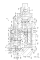
- the mirror unit 2 has a mirror device (optical device) 20, an optical function member 13, a fixed mirror 16 and a stress relieving substrate 17.
- the mirror device 20 includes a base 21, a movable mirror 22, and a drive unit 23.
- the base 21 has a first surface 21a (surface on one side in the Z-axis direction) and a second surface 21b opposite to the first surface 21a. Each of the first surface 21 a and the second surface 21 b is a main surface of the base 21.
- the base 21 has, for example, a rectangular plate shape, and has a size of, for example, about 10 mm ⁇ 15 mm ⁇ 0.35 mm (thickness).
- the movable mirror 22 has a mirror surface (optical function portion) 22a and a movable portion 22b in which the mirror surface 22a is disposed.
- the movable mirror 22 (movable portion 22b) is supported by the base 21 so as to be movable along a Z-axis direction (a predetermined direction perpendicular to the first surface) perpendicular to the first surface 21a.
- the drive unit 23 moves the movable mirror 22 along the Z-axis direction.
- the mirror device 20 is provided with a pair of light passing openings 24 and 25.
- the pair of light passing openings 24 and 25 are disposed on both sides of the movable mirror 22 in the X-axis direction.
- the light passing aperture (first light passing portion) 24 constitutes a first portion of the light path between the beam splitter unit 3 and the fixed mirror 16.
- the light passage opening 25 does not function as a light passage opening.
- FIG. 5 and FIG. 5 is a schematic cross-sectional view of the mirror device 20 shown in FIG. 3.
- the mirror device 20 is schematically shown in a state in which the dimension in the Z-axis direction is larger than the actual size. Is shown.
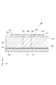
- the base 21, the movable portion 22 b of the movable mirror 22, and the drive portion 23 are configured by an SOI (Silicon On Insulator) substrate (semiconductor substrate) 100. That is, the mirror device 20 is configured by the SOI substrate 100.
- the mirror device 20 is formed, for example, in a rectangular plate shape.
- the SOI substrate 100 has a support layer 101, a device layer 102 and an intermediate layer 103.
- the support layer 101 is a first silicon layer (first semiconductor layer).
- the device layer 102 is a second silicon layer (second semiconductor layer).
- the intermediate layer 103 is an insulating layer disposed between the support layer 101 and the device layer 102.
- the SOI substrate 100 has a support layer 101, an intermediate layer 103 and a device layer 102 in this order from one side in the Z-axis direction.
- the base 21 is configured by the support layer 101, the device layer 102, and part of the intermediate layer 103.
- the first surface 21 a of the base 21 is the surface of the support layer 101 opposite to the intermediate layer 103.
- the second surface 21 b of the base 21 is the surface of the device layer 102 opposite to the intermediate layer 103.
- the support layer 101 constituting the base 21 is thicker than the device layer 102 constituting the base 21.
- the thickness of the support layer 101 constituting the base 21 is, for example, about four times the thickness of the device layer 102 constituting the base 21.
- the second surface 21b of the base 21 and the third surface 13a of the optical function member 13 are bonded to each other (see FIGS. 3 and 4).
- the movable mirror 22 is disposed with a point of intersection between the axis R1 and the axis R2 as a center position (center of gravity).
- the axis R1 is a straight line extending in the X-axis direction.
- the axis R2 is a straight line extending in the Y-axis direction (a second direction perpendicular to the first direction and the third direction).
- the portion of the mirror device 20 other than the portion overlapping the sixth surface 21d of the base 21 described later exhibits a line-symmetrical shape with respect to each of the axis R1 and the axis R2.
- the movable mirror 22 (movable portion 22 b) includes an arrangement portion 221, a frame portion 222, a pair of connecting portions 223, and a beam portion 224.
- the placement portion 221, the frame portion 222, and the pair of connection portions 223 are configured by a part of the device layer 102.
- the placement portion 221 has a circular shape when viewed from the Z-axis direction.
- the placement portion 221 has a central portion 221 a and an outer edge portion 221 b.
- a metal film (metal layer) is formed on the surface 221 as on one side in the Z-axis direction of the central portion 221 a, whereby a mirror surface 22 a is provided.
- the mirror surface 22a extends perpendicularly to the Z-axis direction, and has a circular shape.
- the surface 221 as of the central portion 221 a is a surface on the side of the intermediate layer 103 in the device layer 102.
- the mirror surface 22 a is located on the other side in the Z-axis direction than the first surface 21 a of the base 21.
- the first surface 21a is located on one side in the Z-axis direction relative to the mirror surface 22a.
- the outer edge portion 221 b surrounds the central portion 221 a when viewed from the Z-axis direction.
- the frame portion 222 annularly extends so as to surround the arrangement portion 221 at a predetermined distance from the arrangement portion 221 when viewed in the Z-axis direction.
- the frame portion 222 has, for example, an annular shape when viewed from the Z-axis direction.
- Each of the pair of connecting portions 223 connects the placement portion 221 and the frame portion 222 to each other.
- the pair of connecting portions 223 is disposed on both sides of the disposition portion 221 in the Y-axis direction.
- the beam portion 224 is constituted by the support layer 101 and the intermediate layer 103 disposed on the device layer 102.
- the beam portion 224 is disposed around the mirror surface 22a.
- the beam portion 224 includes an inner beam portion 224a, an outer beam portion 224b, and a pair of connection beam portions 224c.
- the inner beam portion 224a is disposed on the surface on one side in the Z-axis direction of the outer edge portion 221b.
- the inner beam portion 224a surrounds the mirror surface 22a when viewed in the Z-axis direction.
- the outer edge of the inner beam portion 224 a extends along the outer edge of the placement portion 221 at a predetermined distance from the outer edge of the placement portion 221 when viewed in the Z-axis direction.
- the inner edge of the inner beam portion 224a extends along the outer edge of the mirror surface 22a at a predetermined distance from the outer edge of the mirror surface 22a when viewed in the Z-axis direction.
- the end surface 224as on one side in the Z-axis direction in the inner beam portion 224a is located on one side in the Z-axis direction with respect to the mirror surface 22a.
- the outer beam portion 224 b is disposed on the surface on one side in the Z-axis direction of the frame portion 222.
- the outer beam portion 224b surrounds the inner beam portion 224a when viewed in the Z-axis direction, and thus surrounds the mirror surface 22a.
- the outer edge of the outer beam portion 224 b extends along the outer edge of the frame portion 222 at a predetermined distance from the outer edge of the frame portion 222 when viewed in the Z-axis direction.
- the inner edge of the outer beam portion 224 b extends along the inner edge of the frame portion 222 at a predetermined distance from the inner edge of the frame portion 222 when viewed in the Z-axis direction.
- the end surface 224 bs on one side in the Z-axis direction in the outer beam portion 224 b is located on one side in the Z-axis direction with respect to the mirror surface 22 a.
- connection beam portions 224 c are respectively disposed on the surface on one side in the Z-axis direction in the pair of connection portions 223.
- Each connection beam portion 224c connects the inner beam portion 224a and the outer beam portion 224b to each other.
- the end face 224cs on one side in the Z-axis direction in the connection beam portion 224c is located on one side in the Z-axis direction with respect to the mirror surface 22a.
- the thicknesses of the inner beam portion 224a, the outer beam portion 224b, and the connection beam portions 224c in the Z-axis direction are equal to one another. That is, the thickness of the support layer 101 which comprises the inner side beam part 224a, the outer side beam part 224b, and each connection beam part 224c is mutually equal.
- the end surface 224as of the inner beam portion 224a, the end surface 224bs of the outer beam portion 224b, and the end surface 224cs of each connecting beam portion 224c are located on the same plane perpendicular to the Z-axis direction.
- the support layer 101 constituting the inner beam portion 224 a, the outer beam portion 224 b and each connecting beam portion 224 c is thinner than the support layer 101 constituting the base 21.
- the end faces 224as, 224bs, 224cs are located on one side in the Z-axis direction relative to the first surface 21a of the base 21.
- the first surface 21a is located on the other side in the Z-axis direction than the end faces 224as, 224bs, and 224cs.
- the width of the outer beam portion 224b When viewed in the Z-axis direction, the width of the outer beam portion 224b is wider than the width of the inner beam portion 224a.
- the width of the inner beam portion 224a when viewed from the Z-axis direction is the length of the inner beam portion 224a in the direction perpendicular to the extending direction of the inner beam portion 224a, and in the present embodiment, the width of the inner beam portion 224a. It is the length of the inner beam portion 224a in the radial direction.
- the width of each connecting beam portion 224c is larger than the width of each of the inner beam portion 224a and the outer beam portion 224b.
- the width of each connecting beam portion 224c is the length of each connecting beam portion 224c along the extension direction of the inner beam portion 224a.
- the drive unit 23 includes a first elastic support 26, a second elastic support 27, and an actuator 28.
- the first elastic support portion 26, the second elastic support portion 27 and the actuator portion 28 are configured by a part of the device layer 102.
- Each of the first elastic support portion 26 and the second elastic support portion 27 is connected between the base 21 and the movable mirror 22.
- the first elastic support portion 26 and the second elastic support portion 27 support the movable mirror 22 so that the movable mirror 22 (movable portion 22 b) can move along the Z-axis direction.
- the first elastic support portion 26 includes a pair of levers 261, a first link member 262, a second link member 263, a pair of beam members 264, an intermediate member 265, a pair of first torsion bars (first torsion support portions) 266, A pair of second torsion bars (second torsion support portions) 267, a pair of non-linearity relaxation springs 268, and a plurality of electrode support portions 269 are provided.
- the pair of levers 261 are disposed on both sides of the light passage opening 24 in the Y-axis direction, and face each other in the Y-axis direction.
- Each lever 261 has a plate shape extending along a plane perpendicular to the Z-axis direction.
- Each lever 261 includes a first portion 261a, a second portion 261b disposed on the opposite side of the movable mirror 22 with respect to the first portion 261a, and a third portion connected to the first portion 261a and the second portion 261b. And a portion 261c.
- the first portion 261a and the second portion 261b extend along the X-axis direction.
- the length of the first portion 261a in the X-axis direction is shorter than the length of the second portion 261b in the X-axis direction.
- the third portions 261 c of the pair of levers 261 extend so as to be apart from each other as they move away from the movable mirror 22.
- the first link member 262 is bridged between the first end portion 261 d opposite to the movable mirror 22 in the pair of levers 261.
- the first link member 262 has a plate shape extending along a plane perpendicular to the Z-axis direction, and extends along the Y-axis direction.
- the second link member 263 is bridged between the second end 261 e of the pair of levers 261 on the movable mirror 22 side.
- the second link member 263 has a plate shape extending along a plane perpendicular to the Z-axis direction, and extends along the Y-axis direction.
- the width of the second link member 263 in the X-axis direction is narrower than the width of the first link member 262 in the X-axis direction.
- the length of the second link member 263 in the Y-axis direction is shorter than the length of the first link member 262 in the Y-axis direction.
- the pair of beam members 264 are respectively bridged between the second portion 261 b of the pair of levers 261 and the first link member 262.
- Each beam member 264 has a plate shape extending along a plane perpendicular to the Z-axis direction.
- the pair of beam members 264 obliquely extends so as to approach each other as the distance from the movable mirror 22 increases.
- the pair of levers 261, the first link member 262, the second link member 263, and the pair of beam members 264 define the light passage opening 24.
- the light passage opening 24 has a polygonal shape when viewed from the Z-axis direction.
- the light passage opening 24 is, for example, a cavity (hole).
- a material having optical transparency to the measurement light L0 and the laser light L10 may be disposed in the light passage opening 24.
- the intermediate member 265 has a plate shape extending along a plane perpendicular to the Z-axis direction, and extends along the Y-axis direction.
- the intermediate member 265 is disposed between the movable mirror 22 and the second link member 263 (in other words, between the movable mirror 22 and the light passage opening 24).
- the intermediate member 265 is connected to the movable mirror 22 via a non-linearity relaxation spring 268 as described later.
- the pair of first torsion bars 266 is stretched between the first end 261 d of the one lever 261 and the base 21 and between the first end 261 d of the other lever 261 and the base 21. ing. That is, the pair of first torsion bars 266 is connected between the pair of levers 261 and the base 21 respectively.
- Each first torsion bar 266 extends along the Y-axis direction.
- the pair of first torsion bars 266 is disposed on the same center line parallel to the Y-axis direction. In the present embodiment, the center line of each first torsion bar 266 and the center line of the first link member 262 are located on the same straight line.
- each lever 261 is provided with a protruding portion 261 f that protrudes outward in the Y-axis direction, and each first torsion bar 266 is connected to the protruding portion 261 f.
- the pair of second torsion bars 267 is disposed between the second end 261 e of one lever 261 and one end of the intermediate member 265, and the second end 261 e of the other lever 261 and the other end of the intermediate member 265. It is bridged between. That is, the pair of second torsion bars 267 is connected between the pair of levers 261 and the movable mirror 22. Each second torsion bar 267 extends along the Y-axis direction. The pair of second torsion bars 267 are disposed on the same center line parallel to the Y-axis direction.
- a pair of non-linearity relieving springs 268 are connected between the movable mirror 22 and the intermediate member 265. That is, the pair of non-linearity relaxation springs 268 are connected between the movable mirror 22 and the second torsion bar 267.
- Each non-linearity relieving spring 268 has a meandering portion 268a extending in a meandering manner when viewed from the Z-axis direction.
- the meandering portion 268a extends in the Y-axis direction and includes a plurality of linear portions 268b aligned in the X-axis direction and a plurality of folded portions 268c alternately connecting both ends of the plurality of linear portions 268b. .
- One end of the meandering portion 268 a is connected to the intermediate member 265, and the other end of the meandering portion 268 a is connected to the frame portion 222.
- the portion on the side of the frame portion 222 in the meandering portion 268a has a shape along the outer edge of the frame portion 222.
- the non-linearity relaxation spring 268 is configured such that the first torsion bar 266 and the second torsion bar 267 around the Y-axis direction in the deformation amount of the non-linearity relaxation spring 268 around the Y-axis direction when the movable mirror 22 moves in the Z-axis direction. And the deformation of the non-linearity relaxation spring 268 in the X-axis direction is larger than the deformation of each of the first torsion bar 266 and the second torsion bar 267 in the X-axis direction. Is configured.
- the amounts of deformation of the first torsion bar 266, the second torsion bar 267, and the non-linearity relaxation spring 268 around the Y-axis direction mean, for example, the absolute value of the amount of twist (twist angle).
- the amount of deformation of the first torsion bar 266, the second torsion bar 267, and the non-linearity relaxation spring 268 in the X-axis direction means, for example, the absolute value of the amount of bending.
- the amount of deformation of a member about the Y-axis direction means the amount of deformation of the member in the circumferential direction of a circle centered on an axis passing through the center of the member and parallel to the Y-axis.
- the plurality of electrode support portions 269 includes a pair of first electrode support portions 269a, a pair of second electrode support portions 269b, and a pair of third electrode support portions 269c.
- Each electrode support portion 269a, 269b, 269c has a plate shape extending along a plane perpendicular to the Z-axis direction, and extends along the Y-axis direction.
- Each electrode support 269 a, 269 b, 269 c extends from the second portion 261 b of the lever 261 toward the side opposite to the light passage opening 24.
- the pair of first electrode support portions 269a is disposed on the same center line parallel to the Y-axis direction.
- the pair of second electrode support portions 269 b is disposed on the same center line parallel to the Y-axis direction.
- the pair of third electrode support portions 269c is disposed on the same center line parallel to the Y-axis direction.
- the first electrode support 269a, the second electrode support 269b, and the third electrode support 269c are arranged in this order from the movable mirror 22 side.
- the second elastic support portion 27 includes a pair of levers 271, a first link member 272, a second link member 273, a pair of beam members 274, an intermediate member 275, a pair of first torsion bars (first torsion support portions) 276, A pair of second torsion bars (second torsion support portions) 277, a pair of non-linearity relaxation springs 278, and a plurality of electrode support portions 279 are provided.
- the pair of levers 271 are disposed on both sides of the light passage opening 25 in the Y-axis direction, and face each other in the Y-axis direction.
- Each lever 271 has a plate shape extending along a plane perpendicular to the Z-axis direction.
- Each lever 271 includes a first portion 271a, a second portion 271b disposed on the opposite side of the movable mirror 22 with respect to the first portion 271a, and a third portion connected to the first portion 271a and the second portion 271b. And a portion 271c.
- the first portion 271a and the second portion 271b extend along the X-axis direction.
- the length of the first portion 271a in the X-axis direction is shorter than the length of the second portion 271b in the X-axis direction.
- the third portions 271 c of the pair of levers 271 extend so as to be apart from each other as they move away from the movable mirror 22.
- the first link member 272 is bridged between the first end 271 d opposite to the movable mirror 22 in the pair of levers 271.
- the first link member 272 has a plate shape extending along a plane perpendicular to the Z-axis direction, and extends along the Y-axis direction.
- the second link member 273 is bridged between the second end 271 e of the pair of levers 271 on the movable mirror 22 side.
- the second link member 273 has a plate shape extending along a plane perpendicular to the Z-axis direction, and extends along the Y-axis direction.
- the width of the second link member 273 in the X axis direction is narrower than the width of the first link member 272 in the X axis direction.
- the length of the second link member 273 in the Y-axis direction is shorter than the length of the first link member 272 in the Y-axis direction.
- the pair of beam members 274 is bridged between the second portion 271 b of the pair of levers 271 and the first link member 272.
- Each beam member 274 has a plate shape extending along a plane perpendicular to the Z-axis direction.
- the pair of beam members 274 obliquely extends so as to be closer to each other as the distance from the movable mirror 22 is increased.
- the pair of levers 271, the first link member 272, the second link member 273, and the pair of beam members 274 define the light passage opening 25.
- the light passage opening 25 has a polygonal shape when viewed from the Z-axis direction.
- the light passage opening 25 is, for example, a cavity (hole).
- a material having optical transparency to the measurement light L0 and the laser light L10 may be disposed in the light passage opening 25.
- the intermediate member 275 has a plate shape extending along a plane perpendicular to the Z-axis direction, and extends along the Y-axis direction.
- the intermediate member 275 is disposed between the movable mirror 22 and the second link member 273 (in other words, between the movable mirror 22 and the light passage opening 25).
- the intermediate member 275 is connected to the movable mirror 22 via a non-linearity relaxation spring 278 as described later.
- the pair of first torsion bars 276 is stretched between the first end 271 d of the one lever 271 and the base 21 and between the first end 271 d of the other lever 271 and the base 21. ing. That is, the pair of first torsion bars 276 are respectively connected between the pair of levers 271 and the base 21.
- Each first torsion bar 276 extends along the Y-axis direction.
- the pair of first torsion bars 276 are disposed on the same center line parallel to the Y-axis direction. In the present embodiment, the center line of each first torsion bar 276 and the center line of the first link member 272 are located on the same straight line.
- the first end 271d of each lever 271 is provided with a protruding portion 271f protruding outward in the Y-axis direction, and each first torsion bar 276 is connected to the protruding portion 271f.
- the pair of second torsion bars 277 are respectively disposed between the second end 271 e of one lever 271 and one end of the intermediate member 275, and the second end 271 e of the other lever 271 and the other end of the intermediate member 275 It is bridged between. That is, the pair of second torsion bars 277 are connected between the pair of levers 271 and the movable mirror 22 respectively. Each second torsion bar 277 extends along the Y-axis direction. The pair of second torsion bars 277 are disposed on the same center line parallel to the Y-axis direction.
- a pair of non-linearity relief springs 278 are connected between the movable mirror 22 and the intermediate member 275. That is, the pair of non-linearity relaxation springs 278 are connected between the movable mirror 22 and the second torsion bar 277.
- Each non-linearity relieving spring 278 has a serpentine portion 278 a which extends in a serpentine manner when viewed from the Z-axis direction.
- Serpentine portion 278a extends in the Y-axis direction and includes a plurality of linear portions 278b aligned in the X-axis direction, and a plurality of folded portions 278c alternately connecting both ends of the plurality of linear portions 278b. .
- One end of the meandering portion 278 a is connected to the intermediate member 275, and the other end of the meandering portion 278 a is connected to the frame portion 222.
- the portion on the side of the frame portion 222 in the meandering portion 278 a has a shape along the outer edge of the frame portion 222.
- the non-linearity relaxation spring 278 is configured such that the first torsion bar 276 and the second torsion bar 277 around the Y-axis direction have the amount of deformation of the non-linearity relaxation spring 278 around the Y-axis direction when the movable mirror 22 moves in the Z-axis direction. And the deformation amount of the non-linearity relaxation spring 278 in the X-axis direction is larger than the deformation amount of each of the first torsion bar 276 and the second torsion bar 277 in the X-axis direction. Is configured.
- the plurality of electrode support parts 279 includes a pair of first electrode support parts 279a, a pair of second electrode support parts 279b, and a pair of third electrode support parts 279c.
- Each of the electrode support portions 279a, 279b, and 279c has a plate shape extending along a plane perpendicular to the Z-axis direction, and extends along the Y-axis direction.
- Each electrode support portion 279a, 279b, 279c extends from the second portion 271b of the lever 271 toward the side opposite to the light passage opening 25.
- the pair of first electrode support portions 279a is disposed on the same center line parallel to the Y-axis direction.
- the pair of second electrode support portions 279 b is disposed on the same center line parallel to the Y-axis direction.
- the pair of third electrode support portions 279 c is disposed on the same center line parallel to the Y-axis direction.
- the first electrode support 279a, the second electrode support 279b, and the third electrode support 279c are arranged in this order from the movable mirror 22 side.
- the actuator unit 28 moves the movable mirror 22 along the Z-axis direction.
- the actuator unit 28 includes a fixed comb electrode 281, a movable comb electrode 282, a fixed comb electrode 283, and a movable comb electrode 284.
- the positions of the fixed comb electrodes 281 and 283 are fixed.
- the movable comb electrodes 282 and 284 move as the movable mirror 22 moves.
- the fixed comb electrode 281 is provided on part of the surface of the device layer 102 of the base 21 facing the electrode support 269.
- the fixed comb electrode 281 has a plurality of fixed comb teeth 281 a extending along a plane perpendicular to the Y-axis direction. These fixed comb teeth 281 a are arranged side by side at a predetermined interval in the Y-axis direction.
- the movable comb electrode 282 is a surface on the movable mirror 22 side in each first electrode support 269a, a surface on both sides in the X axis direction in each second electrode support 269b, and a movable mirror in each third electrode support 269c. It is provided on the surface on the 22 side.
- the movable comb electrode 282 has a plurality of movable comb teeth 282 a extending along a plane perpendicular to the Y-axis direction. These movable comb teeth 282a are arranged side by side at a predetermined interval in the Y-axis direction.
- a plurality of fixed comb teeth 281a and a plurality of movable comb teeth 282a are alternately arranged. That is, the fixed comb teeth 281 a of the fixed comb electrode 281 are located between the movable comb teeth 282 a of the movable comb electrode 282.
- the fixed comb teeth 281a and the movable comb teeth 282a adjacent to each other face each other in the Y-axis direction.
- the distance between the adjacent fixed comb teeth 281 a and the movable comb teeth 282 a is, for example, about several ⁇ m.
- the stationary comb electrode 283 is provided on part of the surface of the device layer 102 of the base 21 facing the electrode support portion 279.
- the fixed comb electrode 283 has a plurality of fixed comb teeth 283 a extending along a plane perpendicular to the Y-axis direction. These fixed comb teeth 283a are arranged side by side at a predetermined interval in the Y-axis direction.
- the movable comb electrode 284 is a surface on the movable mirror 22 side of each first electrode support portion 279a, a surface on both sides in the X axis direction of each second electrode support portion 279b, and a movable mirror in each third electrode support portion 279c. It is provided on the surface on the 22 side.
- the movable comb electrode 284 has a plurality of movable comb teeth 284 a extending along a plane perpendicular to the Y-axis direction. These movable comb teeth 284a are arranged side by side at predetermined intervals in the Y-axis direction.
- a plurality of fixed comb teeth 283 a and a plurality of movable comb teeth 284 a are alternately arranged. That is, the fixed comb teeth 283 a of the fixed comb electrode 283 are located between the movable comb teeth 284 a of the movable comb electrode 284. Adjacent fixed comb teeth 283 a and movable comb teeth 284 a face each other in the Y-axis direction. The distance between the adjacent fixed comb teeth 283 a and the movable comb teeth 284 a is, for example, about several ⁇ m.
- the base 21 is provided with a plurality of electrode pads 211. Each electrode pad 211 is disposed on the surface of the device layer 102 in an opening 213 formed in the first surface 21 a of the base 21 so as to reach the device layer 102. Some of the plurality of electrode pads 211 are electrically connected to the fixed comb electrode 281 or the fixed comb electrode 283 via the device layer 102. Some other ones of the plurality of electrode pads 211 are electrically connected to the movable comb electrode 282 or the movable comb electrode 284 via the first elastic support portion 26 or the second elastic support portion 27. .
- the base 21 is also provided with a pair of electrode pads 212 used as ground electrodes. The pair of electrode pads 212 is disposed on the first surface 21 a so as to be located on both sides of the movable mirror 22 in the Y-axis direction.
- each electrode pad 211 is provided in the opening 213 formed in the surface 101 a on one side in the Z-axis direction of the support layer 101 so as to reach the device layer 102. It is arranged on the surface 102a on one side of the direction.
- the opening 213 has a bottom surface 214 formed by the surface 102 a and a side surface 215 formed by the support layer 101 and the intermediate layer 103.
- the bottom surface 214 has, for example, a rectangular shape.
- the side surface 215 is a first surface 215a continuously extending from the bottom surface 214 and substantially perpendicular to the bottom surface 214, a step surface 215b continuously extending from the first surface 215a substantially parallel to the bottom surface 214, and a step surface 215b.
- a second surface 215c extending substantially perpendicularly to the bottom surface 214.
- the step surface 215 b extends annularly along the edge of the opening 213 when viewed in the Z-axis direction.
- the electrode pad 211 is disposed over the entire surface of the bottom surface 214. Also, the electrode pad 211 extends across the bottom surface 214 and the side surface 215. More specifically, the electrode pad 211 is formed so as to reach the first surface 215 a of the side surface 215 and not reach the step surface 215 b.
- the electrode pad 211 is made of, for example, a metal film (metal layer). This metal film is formed, for example, by sputtering using a hard mask. The metal film forming the electrode pad 211 is thicker than the metal film forming the mirror surface 22 a.
- the base 21 has a groove 216 formed in the surface 101 a of the support layer 101 so as to reach the device layer 102.
- the groove portion 216 extends annularly to surround the opening 213 when viewed in the Z-axis direction.
- the groove portion 216 has, for example, a rectangular ring shape when viewed from the Z-axis direction.
- the provision of the groove portion 216 can electrically insulate the electrode pads 211 from each other. That is, as in the present embodiment, when the metal film constituting the electrode pad 211 is formed to reach the side surface 215 and the electrode pad 211 is in contact with the support layer 101, the electrode pads 211 are connected to the support layer 101. There is a risk of being electrically connected via On the other hand, in the mirror device 20, by providing the groove portion 216, even in such a case, the electrode pads 211 can be electrically insulated reliably.
- an electric signal for moving the movable mirror 22 along the Z-axis direction is input to the drive unit 23 through the lead pin 113 and a wire (not shown) described later.
- a wire (not shown) described later.
- the first torsion bars 266 and 276 and the second torsion bars 267 and 277 are twisted in the first elastic support portion 26 and the second elastic support portion 27, and the first elastic support portion 26 and the second elastic support portion 27 are An elastic force is generated.
- the movable mirror 22 can be reciprocated at the resonance frequency level along the Z-axis direction.
- the drive unit 23 functions as an electrostatic actuator. [Other configuration of mirror unit]
- the optical function member 13 has a third surface 13a (surface on one side in the Z-axis direction) facing the second surface 21b of the base 21; It has the 4th surface 13b on the opposite side to the 3rd surface 13a.
- the optical function member 13 is disposed on the other side of the mirror device 20 in the Z-axis direction.
- the outer edge 13 c of the optical function member 13 is located outside the outer edge 21 c of the base 21. That is, when viewed from the Z-axis direction, the outer edge 13 c of the optical function member 13 surrounds the outer edge 21 c of the base 21.
- the optical function member 13 is integrally formed of a material having transparency to the measurement light L0 and the laser light L10.
- the optical function member 13 is formed of, for example, glass in a rectangular plate shape, and has a size of, for example, about 15 mm ⁇ 20 mm ⁇ 4 mm (thickness).
- the material of the optical function member 13 is, for example, glass when the sensitivity wavelength of the optical module 1 is in the near infrared region, and silicon when the sensitivity wavelength of the optical module 1 is in the mid infrared region. , And the sensitivity wavelength of the light module 1.
- the optical function member 13 is provided with a pair of light transmitting portions 14 and 15.
- the light transmitting portion 14 is a portion of the optical function member 13 facing the light passing opening 24 of the mirror device 20 in the Z-axis direction.
- the light transmitting portion 15 is a portion of the optical function member 13 facing the light passing opening 25 of the mirror device 20 in the Z-axis direction.
- the surface 14a on the mirror device 20 side in the light transmission part 14 and the surface 15a on the mirror device 20 side in the light transmission part 15 are located on the same plane as the third surface 13a.
- the light transmitting portion (second light transmitting portion) 14 constitutes a second portion (portion) of the light path between the beam splitter unit 3 and the fixed mirror 16.
- the light transmitting unit 14 is a portion that corrects an optical path difference generated between an optical path between the beam splitter unit 3 and the movable mirror 22 and an optical path between the beam splitter unit 3 and the fixed mirror 16.
- the light transmission unit 15 does not function as a light transmission unit.
- the optical function member 13 has a fifth surface 13 d facing the movable mirror 22 and the drive unit 23 of the mirror device 20.
- the fifth surface 13 d is located closer to the fourth surface 13 b than the third surface 13 a.
- the fifth surface 13 d extends to the outer edge 13 c of the optical function member 13 when viewed in the Z-axis direction.
- the fifth surface 13 d is a pair of the outer edge 13 c of the optical function member 13 extending in the Y-axis direction while surrounding the end portion of each of the light transmitting portions 14 and 15 on the mirror device 20 side. It extends to each of the opposite sides.
- the third surface 13a of the optical function member 13 is formed by direct bonding (for example, plasma activation bonding, surface-activated room-temperature bonding (SAB), atomic diffusion bonding (ADB: atomic diffusion) Bonding is performed to the second surface 21b of the base 21 by anodic bonding, anodic bonding, fusion bonding, hydrophilic bonding, and the like.
- the third surface 13 a extends to face the plurality of electrode pads 211 and 212 provided on the base 21 on both sides of the fifth surface 13 d in the Y-axis direction.
- the fifth surface 13 d is located closer to the fourth surface 13 b than the third surface 13 a, the fifth surface 13 d is separated from the mirror device 20 in a region facing the movable mirror 22 and the drive unit 23 It will be. Further, the surface 14 a of the light transmitting unit 14 and the surface 15 a of the light transmitting unit 15 respectively face the light passing openings 24 and 25 of the mirror device 20. Thereby, in the mirror unit 2, when the movable mirror 22 reciprocates along the Z-axis direction, the movable mirror 22 and the drive unit 23 are prevented from contacting the optical function member 13.
- the base 21 of the mirror device 20 is provided with a sixth surface 21d separated from the optical function member 13 in a state where the third surface 13a of the optical function member 13 and the second surface 21b of the base 21 are joined to each other. ing.
- the sixth surface 21 d is separated from the optical function member 13 in a region including at least a part of the outer edge of the base 21 when viewed in the Z-axis direction.
- the sixth surface 21 d is formed by removing the device layer 102 and the intermediate layer 103 by etching along one side of the outer edge of the base 21 extending in the Y-axis direction.
- a plurality of reference holes 13 e are formed in the third surface 13 a of the optical function member 13.
- the plurality of reference holes 13 e are formed in the third surface 13 a so as to correspond to the plurality of corner portions of the base 21.
- the portion of the base 21 corresponding to the sixth surface 21d is gripped to handle the mirror device 20 Is performed, and the position of the mirror device 20 in the X-axis direction and the Y-axis direction with reference to the plurality of reference holes 13e formed in the third surface 13a, and the mirror device 20 in a plane perpendicular to the Z-axis direction. Is adjusted.
- the fixed mirror 16 is disposed on the other side (opposite to the mirror device 20) in the Z-axis direction with respect to the optical function member 13, and the base of the mirror device 20 is The position for 21 is fixed.
- the fixed mirror 16 is formed on the fourth surface 13 b of the optical function member 13 by, for example, vapor deposition.
- the fixed mirror 16 has a mirror surface 16a perpendicular to the Z-axis direction.
- the mirror surface 22 a of the movable mirror 22 and the mirror surface 16 a of the fixed mirror 16 face one side (the beam splitter unit 3 side) in the Z-axis direction.
- the fixed mirror 16 is continuously formed on the fourth surface 13 b of the optical function member 13 so as to reflect the light transmitted through the light transmission portions 14 and 15 of the optical function member 13.
- the fixed mirror that reflects the light transmitted through the unit 14 and the fixed mirror that reflects the light transmitted through the light transmission unit 15 may be separately provided.
- the stress relieving substrate 17 is attached to the fourth surface 13 b of the optical function member 13 via the fixed mirror 16.
- the stress relieving substrate 17 is attached to the fixed mirror 16 by, for example, an adhesive.
- the outer edge of the stress relaxation substrate 17 is located outside the outer edge 13 c of the optical function member 13. That is, when viewed from the Z-axis direction, the outer edge of the stress relaxation substrate 17 surrounds the outer edge 13 c of the optical function member 13.
- the thermal expansion coefficient of the stress relaxation substrate 17 is closer to the thermal expansion coefficient of the base 21 of the mirror device 20 (more specifically, the thermal expansion coefficient of the support layer 101) than the thermal expansion coefficient of the optical function member 13.
- the stress relieving substrate 17 is formed of, for example, silicon in a rectangular plate shape, and has a size of, for example, about 16 mm ⁇ 21 mm ⁇ 0.65 mm (thickness).
- the surface of the stress relaxation substrate 17 opposite to the optical function member 13 is, for example, an adhesive on the surface 9 a of the support 9 (Z-axis direction Is attached to the support 9 by being fixed to the surface on one side of the
- Z-axis direction Is attached to the support 9 by being fixed to the surface on one side of the
- the angle of the mirror device 20 in a plane perpendicular to the Z-axis direction is adjusted.
- the second support structure 12 is not shown.
- the first support structure 11 includes a frame 111, a light transmission member 112, and a plurality of lead pins 113.
- the frame 111 is formed to surround the mirror unit 2 when viewed in the Z-axis direction, and is attached to the surface 9 a of the support 9 by an adhesive such as silver wax, for example.
- the frame 111 is made of, for example, a ceramic, and has, for example, a rectangular frame shape.
- the end face 111 a of the frame 111 opposite to the support 9 is located on the opposite side of the support 9 from the first surface 21 a of the base 21 of the mirror device 20.
- the light transmitting member 112 is formed to close the opening of the frame 111, and is attached to the end surface 111a of the frame 111 by, for example, an adhesive.
- the light transmitting member 112 is formed of a material having transparency to the measurement light L0 and the laser light L10, and has, for example, a rectangular plate shape.
- the end face 111 a of the frame 111 is located on the opposite side of the first surface 21 a of the base 21 of the mirror device 20 to the support 9, the light transmitting member 112 is separated from the mirror device 20. become.
- the support 9, the frame 111, and the light transmitting member 112 constitute a package for housing the mirror unit 2.
- Each lead pin 113 is provided on the frame 111 such that one end 113 a is located inside the frame 111 and the other end (not shown) is located outside the frame 111.
- One end 113 a of the lead pin 113 is electrically connected to the electrode pad 211, 212 corresponding to the lead pin 113 in the mirror device 20 by a wire (not shown).
- an electrical signal for moving the movable mirror 22 along the Z-axis direction is input to the drive unit 23 through the plurality of lead pins 113.
- the step surface 111b extending in the X axis direction is formed on the frame 111 on both sides of the optical function member 13 in the Y axis direction, and one end 113a of each lead pin 113 is disposed on the step surface 111b. It is done.
- Each lead pin 113 extends in the Z-axis direction on both sides of the support 9 in the Y-axis direction, and the other end of each lead pin 113 is positioned on the other side in the Z-axis direction relative to the support 9 There is.
- the beam splitter unit 3 is attached to the surface 112 a of the light transmitting member 112 opposite to the mirror device 20 by, for example, an optical adhesive that doubles as an index matching agent.
- the beam splitter unit 3 has a first mirror surface 31, a second mirror surface 32, and a plurality of optical surfaces 33a, 33b, 33c, and 33d.
- the beam splitter unit 3 is configured by bonding a plurality of optical blocks 34 and 35.
- Each of the optical blocks 34 and 35 is formed of a material having the same or similar refractive index as the optical function member 13.
- 10 is a schematic cross-sectional view of the mirror unit 2 and the beam splitter unit 3 shown in FIG. 1. In FIG. 10, for example, the mirror in a state in which the dimension in the Z-axis direction is larger than the actual size. Device 20 is shown schematically.
- the first mirror surface 31 is a mirror surface (for example, a half mirror surface) inclined with respect to the Z-axis direction, and is formed between the optical block 34 and the optical block 35.
- the first mirror surface 31 is a surface parallel to the Y-axis direction and is a surface that forms an angle of 45 ° with the Z-axis direction, and is further away from the light incident portion 4 as it approaches the mirror device 20 It is an inclined surface.
- the first mirror surface 31 has a function of reflecting a part of the measurement light L0 and transmitting the remaining part of the measurement light L0, and a function of reflecting a part of the laser light L10 and transmitting the remaining part of the laser light L10. ing.
- the first mirror surface 31 is formed of, for example, a dielectric multilayer film.
- the first mirror surface 31 overlaps the light passage aperture 24 of the mirror device 20, the light transmission portion 14 of the optical function member 13, and the mirror surface 16a of the fixed mirror 16 when viewed from the Z-axis direction. When viewed from the axial direction, it overlaps with the light incident part 4 (see FIG. 1). That is, the first mirror surface 31 faces the fixed mirror 16 in the Z-axis direction, and faces the light incident part 4 in the X-axis direction.
- the second mirror surface 32 is a mirror surface (for example, a total reflection mirror surface) parallel to the first mirror surface 31, and is optically positioned on the side opposite to the light incident portion 4 with respect to the first mirror surface 31.
- the block 35 is formed.
- the second mirror surface 32 has a function of reflecting the measurement light L0 and a function of reflecting the laser light L10.
- the second mirror surface 32 is formed of, for example, a metal film.
- the second mirror surface 32 overlaps the mirror surface 22a of the movable mirror 22 of the mirror device 20 when viewed in the Z-axis direction, and overlaps the first mirror surface 31 when viewed in the X-axis direction. That is, the second mirror surface 32 faces the movable mirror 22 in the Z-axis direction, and faces the first mirror surface 31 in the X-axis direction.
- the optical surface 33 a is a surface perpendicular to the Z-axis direction, and is formed in the optical block 35 so as to be located on the opposite side to the mirror device 20 with respect to the first mirror surface 31.
- the optical surface 33 b is a surface perpendicular to the Z-axis direction, and is formed in the optical block 35 so as to be located on the mirror device 20 side with respect to the second mirror surface 32.
- the optical surface 33 c is a surface perpendicular to the Z-axis direction, and is formed in the optical block 34 so as to be located on the side of the mirror device 20 with respect to the first mirror surface 31.
- the optical surface 33 b and the optical surface 33 c are located on the same plane.
- the optical surface 33 d is a surface perpendicular to the X-axis direction, and is formed in the optical block 34 so as to be located on the light incident part 4 side with respect to the first mirror surface 31.
- Each of the optical surfaces 33a, 33b, 33c, and 33d has a function of transmitting the measurement light L0 and a function of transmitting the laser light L10.
- the optical surface 33 b and the optical surface 33 c located on the same plane are fixed to the surface 112 a of the light transmitting member 112 by, for example, an optical adhesive, Is attached to
- an optical adhesive Is attached to
- the angle of the beam splitter unit 3 in a plane perpendicular to the Z-axis direction In FIG. 9, the second support structure 12 is not shown.
- the remaining portion of the measurement light L0 is reflected by the first mirror surface 31, and fixed mirror via the optical surface 33c, the light transmitting member 112, the light passing aperture 24 of the mirror device 20, and the light transmitting portion 14 of the optical functional member 13. It reaches 16 mirror surfaces 16a.
- the remaining portion of the measurement light L0 is reflected by the mirror surface 16a of the fixed mirror 16, travels in the opposite direction on the same optical path P2, and passes through the first mirror surface 31.
- Part of the measurement light L0 reflected by the first mirror surface 31 and the remaining part of the measurement light L0 transmitted through the first mirror surface 31 become interference light L1, and the interference light L1 of the measurement light is an optical surface 33a. From the beam splitter unit 3 along the Z-axis direction.
- the laser beam L10 enters the beam splitter unit 3 along the Z-axis direction via the optical surface 33a, a part of the laser beam L10 is reflected by the first mirror surface 31 and the second mirror surface 32, It reaches the mirror surface 22 a of the movable mirror 22 via the surface 33 b and the light transmitting member 112. A part of the laser beam L10 is reflected by the mirror surface 22a of the movable mirror 22, travels in the opposite direction on the same optical path P3, and is reflected by the first mirror surface 31.
- the remaining portion of the laser beam L10 is transmitted through the first mirror surface 31 and fixed via the optical surface 33c, the light transmitting member 112, the light passing aperture 24 of the mirror device 20, and the light transmitting portion 14 of the optical function member 13 It reaches 16 mirror surfaces 16a.
- the remaining portion of the laser beam L10 is reflected by the mirror surface 16a of the fixed mirror 16, travels in the opposite direction on the same optical path P4, and passes through the first mirror surface 31.
- a portion of the laser beam L10 reflected by the first mirror surface 31 and the remaining portion of the laser beam L10 transmitted through the first mirror surface 31 become an interference beam L11, and the interference beam L11 of the laser beam is an optical surface 33a. From the beam splitter unit 3 along the Z-axis direction.
- the light passage aperture 24 of the mirror device 20 includes the first portion P2a of the light path P2 of the measurement light L0 and the light path P4 of the laser light L10.
- the first part P4a of the The light transmitting portion 14 of the optical function member 13 includes a second portion P2b of the light path P2 of the measurement light L0 and a fourth light path P4 of the laser light L10 in the light path between the beam splitter unit 3 and the fixed mirror 16. It constitutes two parts P4b.
- the optical path length of the optical path P1 of the measurement light L0 (optical path length considering the refractive index of each medium through which the optical path passes) and measurement
- the optical path difference between the two optical paths P1 and P2 is corrected so that the difference between the light path L2 and the optical path length of the optical path P2 becomes small.
- the second portion P4b of the optical path P4 of the laser beam L10 by the light transmitting portion 14, the difference between the optical path length of the optical path P3 of the laser beam L10 and the optical path length of the optical path P4 of the laser beam L10 is small.
- the refractive index of the light transmitting portion 14 is equal to the refractive index of each optical block constituting the beam splitter unit 3, and the distance between the first mirror surface 31 and the second mirror surface 32 along the X axis direction. Is equal to the thickness of the light transmitting portion 14 along the Z-axis direction (that is, the distance between the surface 14 a of the light transmitting portion 14 and the fourth surface 13 b of the optical function member 13 along the Z-axis direction).
- the second support structure 12 includes a connection unit 120.
- the connection unit 120 includes a main body 121, a frame 122, and a fixing plate 123.
- the main body portion 121 includes a pair of side wall portions 124 and 125 and a top wall portion 126.
- the pair of side wall portions 124 and 125 are opposed to each other in the X-axis direction.
- An opening 124 a is formed in the side wall portion 124 on one side in the X-axis direction.
- the top wall portion 126 faces the support 9 in the Z-axis direction.
- An opening 126 a is formed in the top wall portion 126.
- the main body portion 121 is integrally formed of, for example, metal.
- the main body portion 121 is provided with a plurality of positioning pins 121 a.
- the main body portion 121 is positioned with respect to the support 9 by fitting the positioning pins 121a to the reference holes 9b and the holes 9c formed in the support 9, respectively, and in that state, the support 9 is formed by, for example, a bolt. Is attached to
- the frame 122 is disposed on the surface of the side wall 124 opposite to the beam splitter unit 3.
- the opening of the frame 122 faces the beam splitter unit 3 through the opening 124 a of the side wall 124.
- the light incident portion 4 is disposed in the frame body 122.
- the fixing plate 123 is a member for fixing the light incident part 4 disposed in the frame 122 to the main body part 121 (details will be described later).
- the second support structure 12 further comprises a holding unit 130.
- the holding unit 130 includes a main body portion 131, a frame 132, and a fixing plate 133.
- the main body portion 131 is attached to the surface of the top wall portion 126 opposite to the support 9.
- the main body portion 131 is positioned with respect to the main body portion 121 of the connection unit 120 by a plurality of positioning pins 131a, and in that state, is attached to the top wall portion 126 by, for example, a bolt.
- a recess 134 is formed on the surface of the main body portion 131 opposite to the support 9.
- a first light passage hole 135, a second light passage hole 136 and a third light passage hole 137 are formed on the bottom of the recess 134.
- the first light passage hole 135 is formed at a position facing the first mirror surface 31 of the beam splitter unit 3 in the Z-axis direction.
- the second light passage hole 136 is formed on the other side of the first light passage hole 135 in the X-axis direction (that is, the side opposite to the light incident part 4).
- the third light passage hole 137 is formed on the other side of the second light passage hole 136 in the X-axis direction.
- the frame 132 is disposed on the bottom of the recess 134.
- the opening of the frame 132 faces the third light passage hole 137.
- the second light source 7 is disposed in the frame 132.
- the first light detector 6 is disposed on the bottom of the recess 134 so as to face the first light passage hole 135.
- the second light detector 8 is disposed on the bottom of the recess 134 so as to face the second light passage hole 136.
- the fixing plate 133 fixes the first light detector 6 and the second light detector 8 arranged on the bottom of the recess 134 and the second light source 7 arranged on the frame 132 to the main body 131. It is a member (details will be described later).
- the light incident unit 4 has a holder 41 and a collimator lens 42.
- the holder 41 holds the collimator lens 42 and is configured to be able to connect an optical fiber (not shown) for guiding the measurement light L0.
- the collimator lens 42 collimates the measurement light L0 emitted from the optical fiber.
- the optical fiber is connected to the holder 41, the optical axis of the optical fiber coincides with the optical axis of the collimator lens 42.
- the holder 41 is provided with a flange portion 41 a.
- the flange portion 41 a is disposed between the frame body 122 and the fixing plate 123.
- the fixing plate 123 is attached to the side wall 124 by, for example, a bolt, whereby the light incident part 4 disposed in the frame 122 is fixed to the main body 121.
- the light incident unit 4 is disposed on one side of the beam splitter unit 3 in the X-axis direction, and is supported by the second support structure 12.
- the light incidence unit 4 is a beam splitter for measuring light L0 incident from the first light source via the measuring object or measuring light L0 emitted from the measuring object (in the present embodiment, the measuring light L0 guided by the optical fiber) The light is incident on the unit 3.
- a filter 54 is attached to the frame 122.
- the filter 54 has a function of cutting the laser beam L10.
- the filter 54 is disposed in the opening 124 a of the side wall portion 124 in a state of being inclined with respect to the optical axis of the light incident portion 4.
- the filter 54 blocks the opening of the frame 122 when viewed in the X-axis direction.
- the filter 54 is disposed between the light incident part 4 and the beam splitter unit 3 and is supported by the second support structure 12 in a state of being inclined with respect to the optical axis of the light incident part 4 .
- the optical surface of the filter 54 is a surface parallel to the Z-axis direction, and forms an angle of 10 ° to 20 ° with the Y-axis direction.
- the optical axis of the light incident part 4 is parallel to the X-axis direction.
- the filter 54 is inclined with respect to the optical axis of the light incident portion 4, light in the same wavelength band as the laser light L10 is reflected to the outside of the interference optical system, and the light becomes stray light. It can be reliably prevented.
- light of the same wavelength band as the laser light L10 emitted from the beam splitter unit 3 along the X-axis direction is reflected by the filter 54 and a pair of light beams in the main portion 121 of the second support structure 12
- the light is taken out of the interference optical system from between the side wall portions 124 and 125. Thereby, the light can be reliably prevented from becoming stray light.
- the first light detector 6 has a holder 61, a light detection element 62, and a condenser lens 63.
- the holder 61 holds the light detection element 62 and the condenser lens 63.
- the light detection element 62 detects the interference light L1 of the measurement light.
- the light detection element 62 is, for example, an InGaAs photodiode.
- the condenser lens 63 condenses the interference light L 1 of the measurement light incident on the light detection element 62 on the light detection element 62.
- the optical axis of the light detection element 62 and the optical axis of the condensing lens 63 coincide with each other.
- the holder 61 is provided with a flange portion 61 a.
- the flange portion 61 a is disposed between the bottom surface of the recess 134 of the main body portion 131 and the fixing plate 133.
- the fixing plate 133 is attached to the main body portion 131 by, for example, a bolt, whereby the first light detector 6 disposed on the bottom surface of the recess 134 is fixed to the main body portion 131.
- the first light detector 6 is disposed on one side of the beam splitter unit 3 in the Z-axis direction, and is supported by the second support structure 12.
- the first light detector 6 is opposed to the first mirror surface 31 of the beam splitter unit 3 in the Z-axis direction.
- the first light detector 6 detects the interference light L 1 of the measurement light emitted from the beam splitter unit 3.
- the second light detector 8 has a holder 81, a light detection element 82, and a condenser lens 83.
- the holder 81 holds the light detection element 82 and the condenser lens 83.
- the light detection element 82 detects the interference light L11 of the laser light.
- the light detection element 82 is, for example, a Si photodiode.
- the condenser lens 83 condenses the interference light L11 of the laser beam incident on the light detection element 82 on the light detection element 82.
- the optical axis of the light detection element 82 and the optical axis of the condensing lens 83 coincide with each other.
- the holder 81 is provided with a flange portion 81 a.
- the flange portion 81 a is disposed between the bottom surface of the recess 134 of the main body portion 131 and the fixing plate 133.
- the fixing plate 133 is attached to the main body 131 by, for example, a bolt, whereby the second light detector 8 disposed on the bottom surface of the recess 134 is fixed to the main body 131.
- the second light detector 8 is disposed on one side of the beam splitter unit 3 in the Z-axis direction, and is supported by the second support structure 12.
- the second light detector 8 detects the interference light L11 of the laser light emitted from the beam splitter unit 3.
- the second light source 7 has a holder 71, a light emitting element 72, and a collimator lens 73.
- the holder 71 holds the light emitting element 72 and the collimator lens 73.
- the light emitting element 72 emits a laser beam L10.
- the light emitting element 72 is, for example, a semiconductor laser such as a VCSEL.
- the collimator lens 73 collimates the laser beam L10 emitted from the light emitting element 72.
- the optical axis of the light emitting element 72 and the optical axis of the collimator lens 73 coincide with each other.
- the holder 71 is provided with a flange portion 71 a.
- the flange portion 71 a is disposed between the frame 132 and the fixing plate 133.
- the fixing plate 133 is attached to the main body 131 by, for example, a bolt, whereby the second light source 7 disposed in the frame 132 is fixed to the main body 131.
- the second light source 7 is disposed on one side of the beam splitter unit 3 in the Z-axis direction, and is supported by the second support structure 12.
- the second light source 7 emits a laser beam L10 to be incident on the beam splitter unit 3.
- the holding unit 130 the first light detector (first light device) 6, the second light detector (second light device) 8, and the second light source (third light device) 7 are on the same side. And the first light detector 6, the second light detector 8, and the second light source 7 are arranged in the order of the first light detector 6, the second light detector 8, and the second light source 7. Hold In the present embodiment, the holding unit 130 is configured such that, on one side of the beam splitter unit 3 in the Z-axis direction, the first light detector 6, the second light detector 8 and the second light source 7 are on the other side in the Z-axis direction. The first light detector 6, the second light detector 8, and the second light source 7 are held so as to be directed to the beam splitter unit 3 side.
- the holding unit 130 is arranged such that the first light detector 6, the second light detector 8 and the second light source 7 are arranged in this order from one side in the X-axis direction (that is, the light incident portion 4 side). The first light detector 6, the second light detector 8 and the second light source 7 are held.
- the first mirror 51, the second mirror 52 and the third mirror 53 are attached to the main body portion 131 of the holding unit 130.
- the first mirror 51 is held by the holding unit 130 so as to be located on the opposite side of the first light passing hole 135 with respect to the first light detector 6.
- the second mirror 52 is held by the holding unit 130 so as to be located on the opposite side of the second light passing hole 136 from the second light detector 8.
- the third mirror 53 is held by the holding unit 130 so as to be located on the opposite side of the third light passage hole 137 from the second light source 7.
- the first mirror 51 has a function of transmitting the measurement light L0 and reflecting the laser light L10, and is a dichroic mirror inclined with respect to the optical axis of the first light detector 6.
- the first mirror 51 is disposed between the beam splitter unit 3 and the first light detector 6. That is, the first mirror 51 is disposed to face the beam splitter unit 3 and the first light detector 6.
- the optical surface of the first mirror 51 is a surface parallel to the Y-axis direction and that forms an angle of 45 ° with the Z-axis direction.
- the optical axis of the first light detector 6 is parallel to the Z-axis direction.
- the second mirror 52 has a function of reflecting a part of the laser beam L10 and transmitting the remaining part of the laser beam L10, and is a mirror (for example, a half mirror) parallel to the first mirror 51.
- the second mirror 52 is disposed so as to overlap the first mirror 51 when viewed in the X-axis direction and to overlap the second light detector 8 when viewed in the Z-axis direction. That is, the second mirror 52 is disposed to face the first mirror 51 and the second light detector 8.
- the optical surface of the second mirror 52 is a surface parallel to the Y-axis direction and that forms an angle of 45 ° with the Z-axis direction.
- the third mirror 53 has a function of reflecting the laser light L10, and is a mirror (for example, a total reflection mirror) parallel to the second mirror 52.
- the third mirror 53 is disposed so as to overlap the second mirror 52 when viewed in the X-axis direction and to overlap the second light source 7 when viewed in the Z-axis direction. That is, the third mirror 53 is disposed to face the second mirror 52 and the second light source 7.
- the optical surface of the third mirror 53 is a surface parallel to the Y-axis direction and a surface that forms an angle of 45 ° with the Z-axis direction.
- An aperture 55 is attached to the main body portion 131 of the holding unit 130.
- the aperture 55 is held by the holding unit 130 so as to be located between the first mirror 51 and the first light detector 6.
- the aperture 55 is a member having an opening having a circular shape when viewed in the Z-axis direction, and is disposed in the first light passage hole 135.
- the interference light L1 of the measurement light emitted from the beam splitter unit 3 along the Z-axis direction passes through the first mirror 51, enters the first light detector 6 through the aperture 55, and detects the first light. Is detected by the sensor 6.
- the laser beam L10 emitted from the second light source 7 is reflected by the third mirror 53, passes through the second mirror 52, is reflected by the first mirror 51, and is transmitted to the beam splitter unit 3 along the Z axis direction. It will be incident.
- the interference light L11 of the laser light emitted from the beam splitter unit 3 along the Z-axis direction is reflected by the first mirror 51 and the second mirror 52 and enters the second light detector 8, and the second light detector 8 is detected.
- the first surface 21a (surface on one side in the Z-axis direction) of the base 21 is located on one side of the mirror surface 22a.
- the mirror surface 22a can be protected by the base 21.
- damage to the mirror surface 22a due to direct contact at the time of transportation or the like can be suppressed.
- the support layer 101 constituting the base 21 is thicker than the device layer 102 constituting the base 21.
- the amount of projection of the base 21 with respect to the mirror surface 22a can be secured, and the mirror surface 22a can be effectively protected by the base 21. Therefore, according to the mirror device 20, the reliability can be enhanced.
- the first surface 21a of the base 21 is located on one side of the mirror surface 22a
- the entire first surface 21a is located on one side in the Z-axis direction relative to the mirror surface 22a.
- the entire mirror surface 22a is located on the other side in the Z-axis direction than the first surface 21a.
- the “surface on one side in the Z-axis direction in the base” is, in other words, “the end surface on one side in the Z-axis direction in the base” or “the surface of the base, located on the most side in the Z-axis direction Surface to be
- the end surface (end surface 224 as, 224 bs, 224 cs) on one side in the Z-axis direction in the beam portion 224 is located on one side of the mirror surface 22 a. Thereby, the mirror surface 22 a can be protected also by the beam portion 224. Furthermore, deformation during movement of the movable portion 22b can be suppressed by the beam portion 224.
- the beam portion 224 includes an inner beam portion 224a disposed on the surface on one side of the disposition portion 221 so as to extend along the outer edge of the disposition portion 221 when viewed in the Z-axis direction. .
- the inner beam portion 224a is disposed near the mirror surface 22a, so that the mirror surface 22a can be protected more effectively.
- the inner beam portion 224a is disposed on the placement portion 221, deformation of the placement portion 221 can be more suitably suppressed.
- the beam portion 224 has an outer beam portion 224 b disposed on the surface on one side of the frame portion 222 so as to extend along the frame portion 222 when viewed in the Z-axis direction. Thereby, the mirror surface 22a can be protected more effectively by the beam portion 224. Furthermore, the deformation of the frame portion 222 can be suppressed by the outer beam portion 224b, and consequently, the deformation of the arrangement portion 221 caused by the deformation of the frame portion 222 can be suppressed.
- the support layer 101 constituting the beam portion 224 is thinner than the support layer 101 constituting the base 21. Accordingly, it is possible to suppress the projection of the beam portion 224 from the base 21 during the movement of the movable portion 22b, and it is possible to increase the amount of movement of the movable portion 22b in the Z-axis direction.
- the base 21 is formed with a groove portion 216 which extends from the surface 101 a of the support layer 101 (surface on one side in the Z-axis direction) to the device layer 102 and extends so as to surround the opening 213 when viewed from the Z-axis direction. It is done.
- the electrical insulation of the electrode pad 211 can be ensured by the groove portion 216, and the reliability can be further enhanced.
- An electrode pad 211 extends across the bottom 214 and the side 215 of the opening 213. As a result, the area of the electrode pad 211 can be increased.
- the metal layer constituting the electrode pad 211 is thicker than the metal layer constituting the mirror surface 22a. In this case, deformation of the mirror surface 22a can be suppressed, and electrical connection to the electrode pad 211 can be ensured. That is, in order to suppress the warp of the mirror surface 22a, it is preferable that the metal layer constituting the mirror surface 22a be thin. When the metal layer constituting the electrode pad 211 is thick, bonding performance in the wire bonding process can be enhanced. If the electrode pad 211 is too thin, there is a concern that a wire can not be provided or sufficient adhesion can not be obtained, but the mirror device 20 can suppress such a situation.
- “Correction of the optical path length difference” means the optical path length of the optical path between the beam splitter unit 3 and the movable mirror 33 (the optical path length taking into consideration the refractive index of each medium through which the optical path passes) This means reducing the difference between the fixed path 16 and the optical path length of the optical path.
- the mirror surface 22 a is disposed on the surface of the device layer 102 opposite to the intermediate layer 103, and the base 21 is the surface of the support layer 101 opposite to the intermediate layer 103.
- the mirror surface 22 a is disposed closer to the optical function member 13 as compared to the structure “joined to the third surface 13 a of the optical function member 13”.
- Such a configuration is particularly effective when the light transmission unit 14 corrects the optical path length difference. That is, for example, the reference position in the case of reciprocating the movable mirror 22 along the Z-axis direction can be easily aligned (with a small amount of operation) on the third surface 13 a of the optical function member 13. Therefore, a sufficient light interference signal can be acquired while suppressing the amount of reciprocating movement of the movable mirror 22 along the Z-axis direction. [Modification]
- each structure are employable not only in the material and shape which were mentioned above but various materials and shapes.
- each of the arrangement portion 221 and the mirror surface 22a may have an arbitrary shape such as a rectangular shape or an octagonal shape when viewed from the Z-axis direction.
- the frame portion 222 may have an arbitrary ring shape such as a rectangular ring shape or an octagonal ring shape when viewed from the Z-axis direction.
- Each of the light passage opening 24 and the light passage opening 25 may have any shape such as a circular shape or an octagonal shape when viewed from the Z-axis direction.
- the mirror device 20 may have a hole or a notch formed in the base 21 as a first light passage instead of the light passage opening 24 or the light passage opening 25.
- the semiconductor substrate constituting the mirror device 20 may not necessarily be an SOI substrate, as long as it is a substrate having the first semiconductor layer, the insulating layer, and the second semiconductor layer in this order from one side in the Z-axis direction.
- Each of the inner beam portion 224a, the outer beam portion 224b and the connection beam portion 224c may be formed in any shape.
- the beam portion may extend obliquely with respect to the X-axis direction or the Y-axis direction, or may extend in a zigzag manner.
- the arrangement, number, length, width and thickness of each beam may be set arbitrarily.
- the thicknesses of the inner beam portion 224a, the outer beam portion 224b, and the connection beam portion 224c may be different from each other. At least one of these beams may be omitted.
- the beam portion 224 may not surround the mirror surface 22 a when viewed in the Z-axis direction.
- the thickness of the support layer 101 constituting the beam portion 224 may be the same as the thickness of the support layer 101 constituting the base 21.
- the shapes of the first torsion bars 266 and 276 and the second torsion bars 267 and 277 are not limited, and may be any shape such as a bar.
- the electrode pad 211 may be disposed only on the bottom surface 214 of the opening 213 and may not reach the side surface 215. In this case, the groove 216 may be omitted.
- the second surface 21 b of the base 21 and the third surface 13 a of the optical function member 13 may be bonded to each other by means other than direct bonding (for example, an adhesive such as a UV curing resin).
- the fixed mirror 16 may be separated from the fourth surface 13 b of the optical function member 13 as long as the fixed mirror 16 is disposed on the opposite side of the optical device 13 with respect to the optical function member 13.
- the optical device of the present disclosure is not limited to a mirror device, and may be an optical device in which another optical functional unit other than the mirror surface 22a is disposed on the movable unit 22b. As another optical function part, a lens etc. are mentioned, for example.
- the drive unit 23 of the mirror device 20 may have three or more elastic supports that elastically support the movable mirror 22.
- the actuator unit 28 is not limited to the electrostatic actuator, and may be, for example, a piezoelectric actuator, an electromagnetic actuator, or the like.
- the moving direction (predetermined direction) of the movable portion 22b is a direction perpendicular to the first surface 21a of the base 21. However, the moving direction may be a direction intersecting the first surface 21a.
- the mirror device 20 is not limited to one that constitutes an FTIR, and may constitute another optical system. Each configuration in the above-described one embodiment or modification can be arbitrarily applied to each configuration in the other embodiment or modification.
Abstract
光学デバイスでは、ベース及び可動部は、第1半導体層、絶縁層及び第2半導体層を所定方向における一方の側からこの順に有する半導体基板によって構成されている。ベースは、第1半導体層、絶縁層及び第2半導体層によって構成されている。可動部は、第2半導体層によって構成された配置部を有している。光学機能部は、配置部における一方の側の表面上に配置されている。ベースを構成する第1半導体層は、ベースを構成する第2半導体層よりも厚い。ベースにおける一方の側の表面は、光学機能部よりも一方の側に位置している。
Description
本開示は、光学デバイスに関する。
MEMS(Micro Electro Mechanical Systems)技術によってSOI(Silicon On Insulator)基板に干渉光学系が形成された光学デバイスが知られている(例えば、特許文献1参照)。このような光学デバイスは、高精度な光学配置が実現されたFTIR(フーリエ変換型赤外分光分析器)を提供し得るため、注目されている。
上述したような光学デバイスでは、干渉光学系を構成する可動ミラーが、SOI基板の主面に沿って移動する。これに対し、可動ミラーのミラー面の大型化を図るために、可動ミラーがSOI基板の主面に垂直な方向に沿って移動する構成を採用することが考えられる。しかし、単にそのような構成を採用しただけでは、ミラー面を十分に保護することができず、デバイスとしての信頼性が低下するおそれがある。
本開示の一側面は、信頼性の高い光学デバイスを提供することを目的とする。
本開示の一側面に係る光学デバイスは、主面を有するベースと、主面と交差する所定方向に沿って移動可能となるようにベースにおいて支持された可動部と、可動部上に配置された光学機能部と、を備え、ベース及び可動部は、第1半導体層、絶縁層及び第2半導体層を所定方向における一方の側からこの順に有する半導体基板によって構成されており、ベースは、第1半導体層、絶縁層及び第2半導体層によって構成されており、可動部は、第2半導体層によって構成された配置部を有し、光学機能部は、配置部における一方の側の表面上に配置されており、ベースを構成する第1半導体層は、ベースを構成する第2半導体層よりも厚く、ベースにおける一方の側の表面は、光学機能部よりも一方の側に位置している。
この光学デバイスでは、ベースにおける一方の側の表面が、光学機能部よりも一方の側に位置している。これにより、ベースによって光学機能部を保護することができ、例えば、運搬時等における直接的な接触によって光学機能部が損傷するのを抑制することができる。更に、この光学デバイスでは、ベースを構成する第1半導体層が、ベースを構成する第2半導体層よりも厚い。これにより、光学機能部に対するベースの突出量を確保することができ、ベースによって光学機能部を効果的に保護することができる。よって、この光学デバイスによれば、信頼性を高めることができる。
可動部は、光学機能部の周辺に配置された梁部を更に有し、梁部は、第2半導体層上に配置された第1半導体層及び絶縁層によって構成されており、梁部における一方の側の端面は、光学機能部よりも一方の側に位置していてもよい。この場合、梁部によっても光学機能部を保護することができる。更に、梁部によって可動部の移動中の変形を抑制することもできる。
梁部は、所定方向から見た場合に配置部の外縁に沿って延在するように、配置部における一方の側の表面上に配置されていてもよい。この場合、梁部を光学機能部の近くに配置することができ、光学機能部をより効果的に保護することができる。更に、梁部が配置部上に配置されるため、配置部の変形をより好適に抑制することができる。
可動部は、所定方向から見た場合に配置部を囲む枠部と、配置部と枠部とを互いに連結する連結部と、を更に有し、枠部及び連結部は、第2半導体層によって構成されており、梁部は、所定方向から見た場合に枠部に沿って延在するように、枠部における一方の側の表面上に配置されていてもよい。この場合、梁部によって光学機能部をより一層効果的に保護することができる。更に、梁部によって枠部の変形を抑制することができ、ひいては枠部の変形に起因する配置部の変形を抑制することができる。
梁部を構成する第1半導体層は、ベースを構成する第1半導体層よりも薄くてもよい。この場合、可動部の移動中に梁部がベースから突出するのを抑制することができ、所定方向における可動部の移動量を増加させることが可能となる。
本開示の一側面に係る光学デバイスは、ベースに設けられた電極パッドを更に備え、電極パッドは、第1半導体層における一方の側の表面から第2半導体層に至るようにベースに形成された開口内において、第2半導体層における一方の側の表面上に配置されており、ベースには、第1半導体層における一方の側の表面から第2半導体層に至り、所定方向から見た場合に開口を囲むように延在する溝部が形成されていてもよい。この場合、溝部によって電極パッドの電気的絶縁性を確実化することができ、信頼性を一層高めることができる。
電極パッドは、開口の底面及び側面にわたって延在していてもよい。この場合、電極パッドを大面積化することができる。
電極パッド及び光学機能部の各々は、金属層によって構成されており、電極パッドを構成する金属層は、光学機能部を構成する金属層よりも厚くてもよい。この場合、光学機能部の変形を抑制することができると共に、電極パッドへの電気的接続を確実化することが可能となる。
本開示の一側面に係るミラーユニットは、上記光学デバイスと、光学デバイスに対して所定方向における他方の側に配置された光学機能部材と、光学機能部材に対して他方の側に配置された固定ミラーと、を備え、光学機能部は、可動部と共に可動ミラーを構成するミラー面であり、光学デバイスには、可動ミラー及び固定ミラーと共に干渉光学系を構成するビームスプリッタユニットと固定ミラーとの間の光路の第1部分を構成する第1光通過部が設けられており、光学機能部材には、ビームスプリッタユニットと固定ミラーとの間の光路の第2部分を構成する第2光通過部が設けられており、第2光通過部は、ビームスプリッタユニットと可動ミラーとの間の光路と、ビームスプリッタユニットと固定ミラーとの間の光路と、の間に生じる光路差を補正する。
このミラーユニットでは、上述した理由により、信頼性を高めることができる。また、光学機能部材の第2光通過部によって、ビームスプリッタユニットと可動ミラーとの間の光路と、ビームスプリッタユニットと固定ミラーとの間の光路との間に生じる光路長差を補正することができる。更に、このミラーユニットでは、ミラー面が光学機能部材の近くに配置されている。このような構成は、光学機能部材の第2光通過部によって光路長差を補正する場合に特に有効である。
本開示の一側面によれば、信頼性の高い光学デバイスを提供することができる。
以下、本開示の実施形態について、図面を参照して詳細に説明する。なお、各図において同一又は相当部分には同一符号を付し、重複する部分を省略する。
[光モジュールの構成]
[光モジュールの構成]
図1に示されるように、光モジュール1は、ミラーユニット2と、ビームスプリッタユニット3と、光入射部4と、第1光検出器6と、第2光源7と、第2光検出器8と、支持体9と、第1支持構造11と、第2支持構造12と、を備えている。ミラーユニット2は、Z軸方向(所定方向、第1方向)における支持体9の一方の側に配置されており、例えば接着剤によって、支持体9に取り付けられている。支持体9は、例えば銅タングステンによって形成されており、例えば矩形板状を呈している。ミラーユニット2は、Z軸方向に沿って移動する可動ミラー22と、位置が固定された固定ミラー16と、を含んでいる(詳細については後述する)。なお、Z軸方向は、例えば鉛直方向であり、Z軸方向における一方の側は、例えば上側である。
ビームスプリッタユニット3は、Z軸方向におけるミラーユニット2の一方の側に配置されており、第1支持構造11によって支持されている。第1支持構造11は、例えば接着剤によって、支持体9に取り付けられている。光入射部4は、X軸方向(第1方向に垂直な第3方向)におけるビームスプリッタユニット3の一方の側に配置されており、第2支持構造12によって支持されている。第1光検出器6、第2光源7及び第2光検出器8は、Z軸方向におけるビームスプリッタユニット3の一方の側に配置されており、第2支持構造12によって支持されている。第2支持構造12は、例えばボルトによって、支持体9に取り付けられている。
光モジュール1では、ビームスプリッタユニット3、可動ミラー22及び固定ミラー16によって、測定光L0及びレーザ光L10のそれぞれについて干渉光学系が構成される。測定光L0及びレーザ光L10のそれぞれについて構成される干渉光学系は、例えばマイケルソン干渉光学系である。
測定光L0については、次のように、測定光の干渉光L1が検出される。すなわち、第1光源(図示省略)から測定対象(図示省略)を介して入射した測定光L0又は測定対象から発せられた測定光L0(例えば、測定対象自体の発光等)が、光入射部4からビームスプリッタユニット3に入射すると、当該測定光L0は、ビームスプリッタユニット3において一部及び残部に分割される。そして、測定光L0の一部は、Z軸方向に沿って往復移動する可動ミラー22で反射されてビームスプリッタユニット3に戻る。一方、測定光L0の残部は、固定ミラー16で反射されてビームスプリッタユニット3に戻る。ビームスプリッタユニット3に戻った測定光L0の一部及び残部は、干渉光L1としてビームスプリッタユニット3から出射され、当該測定光の干渉光L1が第1光検出器6によって検出される。
レーザ光L10については、次のように、レーザ光の干渉光L11が検出される。すなわち、第2光源7から出射されたレーザ光L10がビームスプリッタユニット3に入射すると、当該レーザ光L10は、ビームスプリッタユニット3において一部及び残部に分割される。そして、レーザ光L10の一部は、Z軸方向に沿って往復移動する可動ミラー22で反射されてビームスプリッタユニット3に戻る。一方、レーザ光L10の残部は、固定ミラー16で反射されてビームスプリッタユニット3に戻る。ビームスプリッタユニット3に戻ったレーザ光L10の一部及び残部は、干渉光L11としてビームスプリッタユニット3から出射され、当該レーザ光の干渉光L11が第2光検出器8によって検出される。
光モジュール1によれば、レーザ光の干渉光L11の検出結果に基づいて、Z軸方向における可動ミラー22の位置の計測が可能となり、その位置の計測結果、及び測定光の干渉光L1の検出結果に基づいて、測定対象についての分光分析が可能となる。
[ミラーユニットの構成]
[ミラーユニットの構成]
図2、図3及び図4に示されるように、ミラーユニット2は、ミラーデバイス(光学デバイス)20と、光学機能部材13と、固定ミラー16と、応力緩和基板17と、を有している。ミラーデバイス20は、ベース21と、可動ミラー22と、駆動部23と、を含んでいる。
ベース21は、第1表面21a(Z軸方向における一方の側の表面)、及び第1表面21aとは反対側の第2表面21bを有している。第1表面21a及び第2表面21bの各々は、ベース21の主面である。ベース21は、例えば矩形板状を呈しており、例えば10mm×15mm×0.35mm(厚さ)程度のサイズを有している。可動ミラー22は、ミラー面(光学機能部)22aと、ミラー面22aが配置された可動部22bと、を有している。可動ミラー22(可動部22b)は、第1表面21aに垂直なZ軸方向(第1表面に垂直な所定方向)に沿って移動可能となるようにベース21において支持されている。駆動部23は、Z軸方向に沿って可動ミラー22を移動させる。
ミラーデバイス20には、一対の光通過開口24,25が設けられている。一対の光通過開口24,25は、X軸方向における可動ミラー22の両側に配置されている。光通過開口(第1光通過部)24は、ビームスプリッタユニット3と固定ミラー16との間の光路の第1部分を構成している。なお、本実施形態では、光通過開口25は、光通過開口として機能していない。
ここで、ミラーデバイス20の構成について、図2、図5及び図6を参照して詳細に説明する。なお、図5は、図3に示されるミラーデバイス20の模式的な断面図であり、図5には、例えば、Z軸方向における寸法が実際よりも拡大された状態でミラーデバイス20が模式的に示されている。
ベース21、可動ミラー22の可動部22b、及び駆動部23は、SOI(Silicon On Insulator)基板(半導体基板)100によって構成されている。つまり、ミラーデバイス20は、SOI基板100によって構成されている。ミラーデバイス20は、例えば、矩形板状に形成されている。SOI基板100は、支持層101、デバイス層102及び中間層103を有している。支持層101は、第1シリコン層(第1半導体層)である。デバイス層102は、第2シリコン層(第2半導体層)である。中間層103は、支持層101とデバイス層102との間に配置された絶縁層である。SOI基板100は、支持層101、中間層103及びデバイス層102を、Z軸方向における一方の側からこの順に有している。
ベース21は、支持層101、デバイス層102及び中間層103の一部によって構成されている。ベース21の第1表面21aは、支持層101における中間層103とは反対側の表面である。ベース21の第2表面21bは、デバイス層102における中間層103とは反対側の表面である。ベース21を構成する支持層101は、ベース21を構成するデバイス層102よりも厚い。ベース21を構成する支持層101の厚さは、例えば、ベース21を構成するデバイス層102の厚さの4倍程度である。ミラーユニット2では、後述するように、ベース21の第2表面21bと光学機能部材13の第3表面13aとが互いに接合されている(図3及び図4参照)。
可動ミラー22は、軸線R1と軸線R2との交点を中心位置(重心位置)として配置されている。軸線R1は、X軸方向に延在する直線である。軸線R2は、Y軸方向(第1方向及び第3方向に垂直な第2方向)に延在する直線である。Z軸方向から見た場合に、ミラーデバイス20のうち、後述するベース21の第6表面21dと重なる部分以外の部分は、軸線R1及び軸線R2の各々に関して線対称な形状を呈している。
可動ミラー22(可動部22b)は、配置部221、枠部222、一対の連結部223、及び梁部224を有している。配置部221、枠部222及び一対の連結部223は、デバイス層102の一部によって構成されている。配置部221は、Z軸方向から見た場合に円形状を呈している。配置部221は、中央部221a及び外縁部221bを有している。中央部221aにおけるZ軸方向の一方の側の表面221as上には、例えば、金属膜(金属層)が形成されることで、ミラー面22aが設けられている。ミラー面22aは、Z軸方向に垂直に延在し、円形状を呈している。中央部221aの表面221asは、デバイス層102における中間層103側の表面である。ミラー面22aは、ベース21の第1表面21aよりもZ軸方向における他方の側に位置している。換言すれば、第1表面21aは、ミラー面22aよりもZ軸方向における一方の側に位置している。外縁部221bは、Z軸方向から見た場合に中央部221aを囲んでいる。
枠部222は、Z軸方向から見た場合に、配置部221から所定の間隔を空けて配置部221を囲むように、環状に延在している。枠部222は、例えば、Z軸方向から見た場合に円環状を呈している。一対の連結部223の各々は、配置部221と枠部222とを互いに連結している。一対の連結部223は、Y軸方向における配置部221の両側に配置されている。
梁部224は、デバイス層102上に配置された支持層101及び中間層103によって構成されている。梁部224は、ミラー面22aの周辺に配置されている。梁部224は、内側梁部224a、外側梁部224b及び一対の連結梁部224cを有している。内側梁部224aは、外縁部221bにおけるZ軸方向の一方の側の表面上に配置されている。内側梁部224aは、Z軸方向から見た場合にミラー面22aを囲んでいる。例えば、内側梁部224aの外縁は、Z軸方向から見た場合に、配置部221の外縁から所定の間隔を空けて、配置部221の外縁に沿って延在している。内側梁部224aの内縁は、Z軸方向から見た場合に、ミラー面22aの外縁から所定の間隔を空けて、ミラー面22aの外縁に沿って延在している。内側梁部224aにおけるZ軸方向の一方の側の端面224asは、ミラー面22aよりもZ軸方向における一方の側に位置している。
外側梁部224bは、枠部222におけるZ軸方向の一方の側の表面上に配置されている。外側梁部224bは、Z軸方向から見た場合に内側梁部224aを囲んでおり、ひいてはミラー面22aを囲んでいる。例えば、外側梁部224bの外縁は、Z軸方向から見た場合に、枠部222の外縁から所定の間隔を空けて、枠部222の外縁に沿って延在している。外側梁部224bの内縁は、Z軸方向から見た場合に、枠部222の内縁から所定の間隔を空けて、枠部222の内縁に沿って延在している。外側梁部224bにおけるZ軸方向の一方の側の端面224bsは、ミラー面22aよりもZ軸方向における一方の側に位置している。
一対の連結梁部224cは、一対の連結部223におけるZ軸方向の一方の側の表面上にそれぞれ配置されている。各連結梁部224cは、内側梁部224aと外側梁部224bとを互いに連結している。連結梁部224cにおけるZ軸方向における一方の側の端面224csは、ミラー面22aよりもZ軸方向における一方の側に位置している。
Z軸方向における内側梁部224a、外側梁部224b及び各連結梁部224cの厚さは、互いに等しい。つまり、内側梁部224a、外側梁部224b及び各連結梁部224cを構成する支持層101の厚さは、互いに等しい。内側梁部224aの端面224as、外側梁部224bの端面224bs、及び各連結梁部224cの端面224csは、Z軸方向に垂直な同一の平面上に位置している。内側梁部224a、外側梁部224b及び各連結梁部224cを構成する支持層101は、ベース21を構成する支持層101よりも薄い。これにより、端面224as,224bs,224csは、ベース21の第1表面21aよりもZ軸方向における一方の側に位置している。換言すれば、第1表面21aは、端面224as,224bs,224csよりもZ軸方向の他方の側に位置している。
Z軸方向から見た場合に、外側梁部224bの幅は、内側梁部224aの幅よりも広い。Z軸方向から見た場合における内側梁部224aの幅とは、内側梁部224aの延在方向に垂直な方向における内側梁部224aの長さであり、本実施形態では、内側梁部224aの半径方向における内側梁部224aの長さである。この点は、Z軸方向から見た場合における外側梁部224bの幅についても同様である。各連結梁部224cの幅は、内側梁部224a及び外側梁部224bのそれぞれの幅よりも大きい。各連結梁部224cの幅とは、内側梁部224aの延在方向に沿っての各連結梁部224cの長さである。
駆動部23は、第1弾性支持部26、第2弾性支持部27及びアクチュエータ部28を有している。第1弾性支持部26、第2弾性支持部27及びアクチュエータ部28は、デバイス層102の一部によって構成されている。
第1弾性支持部26及び第2弾性支持部27の各々は、ベース21と可動ミラー22との間に接続されている。第1弾性支持部26及び第2弾性支持部27は、可動ミラー22(可動部22b)がZ軸方向に沿って移動可能となるように可動ミラー22を支持している。
第1弾性支持部26は、一対のレバー261、第1リンク部材262、第2リンク部材263、一対の梁部材264、中間部材265、一対の第1トーションバー(第1捩り支持部)266、一対の第2トーションバー(第2捩り支持部)267、一対の非線形性緩和バネ268、及び複数の電極支持部269を有している。
一対のレバー261は、Y軸方向における光通過開口24の両側に配置され、Y軸方向において互いに向かい合っている。各レバー261は、Z軸方向に垂直な平面に沿って延在する板状を呈している。各レバー261は、第1部分261aと、第1部分261aに対して可動ミラー22とは反対側に配置された第2部分261bと、第1部分261a及び第2部分261bに接続された第3部分261cと、を有している。第1部分261a及び第2部分261bは、X軸方向に沿って延在している。X軸方向における第1部分261aの長さは、X軸方向における第2部分261bの長さよりも短い。一対のレバー261の第3部分261cは、可動ミラー22から遠ざかるほど互いに離れるように傾斜して延在している。
第1リンク部材262は、一対のレバー261における可動ミラー22とは反対側の第1端部261d間に掛け渡されている。第1リンク部材262は、Z軸方向に垂直な平面に沿って延在する板状を呈し、Y軸方向に沿って延在している。第2リンク部材263は、一対のレバー261における可動ミラー22側の第2端部261e間に掛け渡されている。第2リンク部材263は、Z軸方向に垂直な平面に沿って延在する板状を呈し、Y軸方向に沿って延在している。X軸方向における第2リンク部材263の幅は、X軸方向における第1リンク部材262の幅よりも狭い。Y軸方向における第2リンク部材263の長さは、Y軸方向における第1リンク部材262の長さよりも短い。
一対の梁部材264は、一対のレバー261の第2部分261bと、第1リンク部材262との間にそれぞれ掛け渡されている。各梁部材264は、Z軸方向に垂直な平面に沿って延在する板状を呈している。一対の梁部材264は、可動ミラー22から遠ざかるほど互いに近付くように傾斜して延在している。一対のレバー261、第1リンク部材262、第2リンク部材263及び一対の梁部材264は、光通過開口24を画定している。光通過開口24は、Z軸方向から見た場合に多角形状を呈している。光通過開口24は、例えば空洞(孔)である。或いは、光通過開口24内には、測定光L0及びレーザ光L10に対して光透過性を有する材料が配置されてもよい。
中間部材265は、Z軸方向に垂直な平面に沿って延在する板状を呈し、Y軸方向に沿って延在している。中間部材265は、可動ミラー22と第2リンク部材263との間(換言すれば、可動ミラー22と光通過開口24との間)に配置されている。中間部材265は、後述するように、非線形性緩和バネ268を介して可動ミラー22に接続されている。
一対の第1トーションバー266は、それぞれ、一方のレバー261の第1端部261dとベース21との間、及び、他方のレバー261の第1端部261dとベース21との間に掛け渡されている。つまり、一対の第1トーションバー266は、一対のレバー261とベース21との間にそれぞれ接続されている。各第1トーションバー266は、Y軸方向に沿って延在している。一対の第1トーションバー266は、Y軸方向に平行な同一の中心線上に配置されている。本実施形態では、各第1トーションバー266の中心線と第1リンク部材262の中心線とは、同一の直線上に位置している。各レバー261の第1端部261dには、Y軸方向における外側に突出した突出部261fが設けられており、各第1トーションバー266は、突出部261fに接続されている。
一対の第2トーションバー267は、それぞれ、一方のレバー261の第2端部261eと中間部材265の一端との間、及び、他方のレバー261の第2端部261eと中間部材265の他端との間に掛け渡されている。つまり、一対の第2トーションバー267は、一対のレバー261と可動ミラー22との間にそれぞれ接続されている。各第2トーションバー267は、Y軸方向に沿って延在している。一対の第2トーションバー267は、Y軸方向に平行な同一の中心線上に配置されている。
一対の非線形性緩和バネ268は、可動ミラー22と中間部材265との間に接続されている。つまり、一対の非線形性緩和バネ268は、可動ミラー22と第2トーションバー267との間に接続されている。各非線形性緩和バネ268は、Z軸方向から見た場合に蛇行して延在する蛇行部268aを有している。蛇行部268aは、Y軸方向に延在し、X軸方向に並ぶ複数の直線状部分268bと、複数の直線状部分268bの両端を交互に連結する複数の折り返し部分268cと、を含んでいる。蛇行部268aの一端は中間部材265に接続され、蛇行部268aの他端は枠部222に接続されている。蛇行部268aにおける枠部222側の部分は、枠部222の外縁に沿った形状を呈している。
非線形性緩和バネ268は、可動ミラー22がZ軸方向に移動した状態において、Y軸方向周りにおける非線形性緩和バネ268の変形量がY軸方向周りにおける第1トーションバー266及び第2トーションバー267の各々の変形量よりも小さくなり、且つ、X軸方向における非線形性緩和バネ268の変形量がX軸方向における第1トーションバー266及び第2トーションバー267の各々の変形量よりも大きくなるように、構成されている。これにより、第1トーションバー266及び第2トーションバー267の捩れ変形に非線形性が生じるのを抑制することができ、当該非線形性に起因する可動ミラー22の制御特性の低下を抑制することができる。なお、Y軸方向周りにおける第1トーションバー266、第2トーションバー267及び非線形性緩和バネ268の変形量とは、例えば、捩れ量(捩れ角度)の絶対値を意味する。X軸方向における第1トーションバー266、第2トーションバー267及び非線形性緩和バネ268の変形量とは、例えば、撓み量の絶対値を意味する。Y軸方向周りにおける或る部材の変形量とは、当該部材の中心を通り且つY軸に平行な軸線を中心とする円の周方向における当該部材の変形量を意味する。これらの点は、後述する第1トーションバー276、第2トーションバー277及び非線形性緩和バネ278についても同様である。
複数の電極支持部269は、一対の第1電極支持部269a、一対の第2電極支持部269b、及び一対の第3電極支持部269cを含んでいる。各電極支持部269a,269b,269cは、Z軸方向に垂直な平面に沿って延在する板状を呈し、Y軸方向に沿って延在している。各電極支持部269a,269b,269cは、レバー261の第2部分261bから、光通過開口24とは反対側に向かって延びている。一対の第1電極支持部269aは、Y軸方向に平行な同一の中心線上に配置されている。一対の第2電極支持部269bは、Y軸方向に平行な同一の中心線上に配置されている。一対の第3電極支持部269cは、Y軸方向に平行な同一の中心線上に配置されている。X軸方向において、第1電極支持部269a、第2電極支持部269b及び第3電極支持部269cは、可動ミラー22側からこの順に並んで配置されている。
第2弾性支持部27は、一対のレバー271、第1リンク部材272、第2リンク部材273、一対の梁部材274、中間部材275、一対の第1トーションバー(第1捩り支持部)276、一対の第2トーションバー(第2捩り支持部)277、一対の非線形性緩和バネ278、及び複数の電極支持部279を有している。
一対のレバー271は、Y軸方向における光通過開口25の両側に配置され、Y軸方向において互いに向かい合っている。各レバー271は、Z軸方向に垂直な平面に沿って延在する板状を呈している。各レバー271は、第1部分271aと、第1部分271aに対して可動ミラー22とは反対側に配置された第2部分271bと、第1部分271a及び第2部分271bに接続された第3部分271cと、を有している。第1部分271a及び第2部分271bは、X軸方向に沿って延在している。X軸方向における第1部分271aの長さは、X軸方向における第2部分271bの長さよりも短い。一対のレバー271の第3部分271cは、可動ミラー22から遠ざかるほど互いに離れるように傾斜して延在している。
第1リンク部材272は、一対のレバー271における可動ミラー22とは反対側の第1端部271d間に掛け渡されている。第1リンク部材272は、Z軸方向に垂直な平面に沿って延在する板状を呈し、Y軸方向に沿って延在している。第2リンク部材273は、一対のレバー271における可動ミラー22側の第2端部271e間に掛け渡されている。第2リンク部材273は、Z軸方向に垂直な平面に沿って延在する板状を呈し、Y軸方向に沿って延在している。X軸方向における第2リンク部材273の幅は、X軸方向における第1リンク部材272の幅よりも狭い。Y軸方向における第2リンク部材273の長さは、Y軸方向における第1リンク部材272の長さよりも短い。
一対の梁部材274は、一対のレバー271の第2部分271bと、第1リンク部材272との間にそれぞれ掛け渡されている。各梁部材274は、Z軸方向に垂直な平面に沿って延在する板状を呈している。一対の梁部材274は、可動ミラー22から遠ざかるほど互いに近付くように傾斜して延在している。一対のレバー271、第1リンク部材272、第2リンク部材273及び一対の梁部材274は、光通過開口25を画定している。光通過開口25は、Z軸方向から見た場合に多角形状を呈している。光通過開口25は、例えば空洞(孔)である。或いは、光通過開口25内には、測定光L0及びレーザ光L10に対して光透過性を有する材料が配置されてもよい。
中間部材275は、Z軸方向に垂直な平面に沿って延在する板状を呈し、Y軸方向に沿って延在している。中間部材275は、可動ミラー22と第2リンク部材273との間(換言すれば、可動ミラー22と光通過開口25との間)に配置されている。中間部材275は、後述するように、非線形性緩和バネ278を介して可動ミラー22に接続されている。
一対の第1トーションバー276は、それぞれ、一方のレバー271の第1端部271dとベース21との間、及び、他方のレバー271の第1端部271dとベース21との間に掛け渡されている。つまり、一対の第1トーションバー276は、一対のレバー271とベース21との間にそれぞれ接続されている。各第1トーションバー276は、Y軸方向に沿って延在している。一対の第1トーションバー276は、Y軸方向に平行な同一の中心線上に配置されている。本実施形態では、各第1トーションバー276の中心線と第1リンク部材272の中心線とは、同一の直線上に位置している。各レバー271の第1端部271dには、Y軸方向における外側に突出した突出部271fが設けられており、各第1トーションバー276は、突出部271fに接続されている。
一対の第2トーションバー277は、それぞれ、一方のレバー271の第2端部271eと中間部材275の一端との間、及び、他方のレバー271の第2端部271eと中間部材275の他端との間に掛け渡されている。つまり、一対の第2トーションバー277は、一対のレバー271と可動ミラー22との間にそれぞれ接続されている。各第2トーションバー277は、Y軸方向に沿って延在している。一対の第2トーションバー277は、Y軸方向に平行な同一の中心線上に配置されている。
一対の非線形性緩和バネ278は、可動ミラー22と中間部材275との間に接続されている。つまり、一対の非線形性緩和バネ278は、可動ミラー22と第2トーションバー277との間に接続されている。各非線形性緩和バネ278は、Z軸方向から見た場合に蛇行して延在する蛇行部278aを有している。蛇行部278aは、Y軸方向に延在し、X軸方向に並ぶ複数の直線状部分278bと、複数の直線状部分278bの両端を交互に連結する複数の折り返し部分278cと、を含んでいる。蛇行部278aの一端は中間部材275に接続され、蛇行部278aの他端は枠部222に接続されている。蛇行部278aにおける枠部222側の部分は、枠部222の外縁に沿った形状を呈している。
非線形性緩和バネ278は、可動ミラー22がZ軸方向に移動した状態において、Y軸方向周りにおける非線形性緩和バネ278の変形量がY軸方向周りにおける第1トーションバー276及び第2トーションバー277の各々の変形量よりも小さくなり、且つ、X軸方向における非線形性緩和バネ278の変形量がX軸方向における第1トーションバー276及び第2トーションバー277の各々の変形量よりも大きくなるように、構成されている。これにより、第1トーションバー276及び第2トーションバー277の捩れ変形に非線形性が生じるのを抑制することができ、当該非線形性に起因する可動ミラー22の制御特性の低下を抑制することができる。
複数の電極支持部279は、一対の第1電極支持部279a、一対の第2電極支持部279b、及び一対の第3電極支持部279cを含んでいる。各電極支持部279a,279b,279cは、Z軸方向に垂直な平面に沿って延在する板状を呈し、Y軸方向に沿って延在している。各電極支持部279a,279b,279cは、レバー271の第2部分271bから、光通過開口25とは反対側に向かって延びている。一対の第1電極支持部279aは、Y軸方向に平行な同一の中心線上に配置されている。一対の第2電極支持部279bは、Y軸方向に平行な同一の中心線上に配置されている。一対の第3電極支持部279cは、Y軸方向に平行な同一の中心線上に配置されている。X軸方向において、第1電極支持部279a、第2電極支持部279b及び第3電極支持部279cは、可動ミラー22側からこの順に並んで配置されている。
アクチュエータ部28は、Z軸方向に沿って可動ミラー22を移動させる。アクチュエータ部28は、固定櫛歯電極281、可動櫛歯電極282、固定櫛歯電極283及び可動櫛歯電極284を有している。固定櫛歯電極281,283の位置は、固定されている。可動櫛歯電極282,284は、可動ミラー22の移動に伴って移動する。
固定櫛歯電極281は、ベース21のデバイス層102における電極支持部269と向かい合う表面の一部に設けられている。固定櫛歯電極281は、Y軸方向に垂直な平面に沿って延在する複数の固定櫛歯281aを有している。これらの固定櫛歯281aは、Y軸方向に所定の間隔を空けて並んで配置されている。
可動櫛歯電極282は、各第1電極支持部269aにおける可動ミラー22側の表面、各第2電極支持部269bにおけるX軸方向の両側の表面、及び、各第3電極支持部269cにおける可動ミラー22側の表面に設けられている。可動櫛歯電極282は、Y軸方向に垂直な平面に沿って延在する複数の可動櫛歯282aを有している。これらの可動櫛歯282aは、Y軸方向に所定の間隔を空けて並んで配置されている。
固定櫛歯電極281及び可動櫛歯電極282においては、複数の固定櫛歯281aと複数の可動櫛歯282aとが互い違いに配置されている。つまり、固定櫛歯電極281の各固定櫛歯281aが可動櫛歯電極282の可動櫛歯282a間に位置している。隣り合う固定櫛歯281aと可動櫛歯282aとは、Y軸方向において互いに向かい合っている。隣り合う固定櫛歯281aと可動櫛歯282aとの間の距離は、例えば数μm程度である。
固定櫛歯電極283は、ベース21のデバイス層102における電極支持部279と向かい合う表面の一部に設けられている。固定櫛歯電極283は、Y軸方向に垂直な平面に沿って延在する複数の固定櫛歯283aを有している。これらの固定櫛歯283aは、Y軸方向に所定の間隔を空けて並んで配置されている。
可動櫛歯電極284は、各第1電極支持部279aにおける可動ミラー22側の表面、各第2電極支持部279bにおけるX軸方向の両側の表面、及び、各第3電極支持部279cにおける可動ミラー22側の表面に設けられている。可動櫛歯電極284は、Y軸方向に垂直な平面に沿って延在する複数の可動櫛歯284aを有している。これらの可動櫛歯284aは、Y軸方向に所定の間隔を空けて並んで配置されている。
固定櫛歯電極283及び可動櫛歯電極284においては、複数の固定櫛歯283aと複数の可動櫛歯284aとが互い違いに配置されている。つまり、固定櫛歯電極283の各固定櫛歯283aが可動櫛歯電極284の可動櫛歯284a間に位置している。隣り合う固定櫛歯283aと可動櫛歯284aとは、Y軸方向において互いに向かい合っている。隣り合う固定櫛歯283aと可動櫛歯284aとの間の距離は、例えば数μm程度である。
ベース21には、複数の電極パッド211が設けられている。各電極パッド211は、デバイス層102に至るようにベース21の第1表面21aに形成された開口213内において、デバイス層102の表面上に配置されている。複数の電極パッド211のうちの幾つかは、デバイス層102を介して、固定櫛歯電極281又は固定櫛歯電極283と電気的に接続されている。複数の電極パッド211のうちの他の幾つかは、第1弾性支持部26又は第2弾性支持部27を介して、可動櫛歯電極282又は可動櫛歯電極284と電気的に接続されている。また、ベース21には、グランド電極として用いられる一対の電極パッド212が設けられている。一対の電極パッド212は、Y軸方向における可動ミラー22の両側に位置するように、第1表面21a上に配置されている。
図11を参照しつつ、電極パッド211の周辺の構成について更に説明する。以下、一の電極パッド211を参照して説明するが、他の電極パッド211についても同様に構成されている。図11に示されるように、各電極パッド211は、デバイス層102に至るように支持層101におけるZ軸方向の一方の側の表面101aに形成された開口213内において、デバイス層102におけるZ軸方向の一方の側の表面102a上に配置されている。
開口213は、表面102aによって構成された底面214と、支持層101及び中間層103によって構成された側面215と、を有している。底面214は、例えば矩形状を呈している。側面215は、底面214に連続して底面214と略垂直に延在する第1面215aと、第1面215aに連続して底面214と略平行に延在する段差面215bと、段差面215bに連続して底面214と略垂直に延在する第2面215cと、を有している。段差面215bは、Z軸方向から見た場合に、開口213の縁に沿って環状に延在している。
電極パッド211は、底面214の全面にわたって配置されている。また、電極パッド211は、底面214及び側面215にわたって延在している。より具体的には、電極パッド211は、側面215の第1面215aに至り、段差面215bには至らないように形成されている。電極パッド211は、例えば、金属膜(金属層)によって構成されている。この金属膜は、例えば、ハードマスクを用いたスパッタリングにより形成される。電極パッド211を構成する金属膜は、ミラー面22aを構成する金属膜よりも厚い。
ベース21は、デバイス層102に至るように支持層101の表面101aに形成された溝部216を有している。溝部216は、Z軸方向から見た場合に開口213を囲むように、環状に延在している。溝部216は、例えば、Z軸方向から見た場合に矩形環状を呈している。溝部216が設けられていることにより、電極パッド211同士を確実に電気的に絶縁することができる。すなわち、本実施形態のように、電極パッド211を構成する金属膜が側面215に至るように形成され、電極パッド211が支持層101に接触している場合、電極パッド211同士が支持層101を介して電気的に接続されてしまうおそれがある。これに対し、ミラーデバイス20では、溝部216が設けられていることにより、そのような場合でも、電極パッド211同士を確実に電気的に絶縁することができる。
以上のように構成されたミラーデバイス20では、後述するリードピン113及びワイヤ(図示省略)を介して、Z軸方向に沿って可動ミラー22を移動させるための電気信号が駆動部23に入力される。これにより、例えば、Z軸方向における一方の側に可動ミラー22が移動するように、互いに向かい合う固定櫛歯電極281と可動櫛歯電極282との間、及び、互いに向かい合う固定櫛歯電極283と可動櫛歯電極284との間に静電気力が生じる。このとき、第1弾性支持部26及び第2弾性支持部27において第1トーションバー266,276、第2トーションバー267,277が捩れて、第1弾性支持部26及び第2弾性支持部27に弾性力が生じる。ミラーデバイス20では、駆動部23に周期的な電気信号を付与することで、Z軸方向に沿って可動ミラー22をその共振周波数レベルで往復動させることができる。このように、駆動部23は、静電アクチュエータとして機能する。
[ミラーユニットの他の構成]
[ミラーユニットの他の構成]
図2、図3、図4及び図7に示されるように、光学機能部材13は、ベース21の第2表面21bと対向する第3表面13a(Z軸方向における一方の側の表面)、及び第3表面13aとは反対側の第4表面13bを有している。光学機能部材13は、ミラーデバイス20に対してZ軸方向における他方の側に配置されている。Z軸方向から見た場合に、光学機能部材13の外縁13cは、ベース21の外縁21cの外側に位置している。つまり、Z軸方向から見た場合に、光学機能部材13の外縁13cは、ベース21の外縁21cを包囲している。光学機能部材13は、測定光L0及びレーザ光L10に対して透過性を有する材料によって一体的に形成されている。光学機能部材13は、例えばガラスによって矩形板状に形成されており、例えば15mm×20mm×4mm(厚さ)程度のサイズを有している。なお、光学機能部材13の材料は、例えば、光モジュール1の感度波長が近赤外領域である場合にはガラス、光モジュール1の感度波長が中赤外領域である場合にはシリコンというように、光モジュール1の感度波長によって選択される。
光学機能部材13には、一対の光透過部14,15が設けられている。光透過部14は、光学機能部材13のうち、Z軸方向においてミラーデバイス20の光通過開口24と対向する部分である。光透過部15は、光学機能部材13のうち、Z軸方向においてミラーデバイス20の光通過開口25と対向する部分である。光透過部14におけるミラーデバイス20側の表面14a、及び光透過部15におけるミラーデバイス20側の表面15aは、第3表面13aと同一平面上に位置している。光透過部(第2光通過部)14は、ビームスプリッタユニット3と固定ミラー16との間の光路の第2部分(一部分)を構成している。光透過部14は、ビームスプリッタユニット3と可動ミラー22との間の光路と、ビームスプリッタユニット3と固定ミラー16との間の光路と、の間に生じる光路差を補正する部分である。なお、本実施形態では、光透過部15は、光透過部として機能していない。
光学機能部材13は、ミラーデバイス20の可動ミラー22及び駆動部23と対向する第5表面13dを有している。第5表面13dは、第3表面13aよりも第4表面13b側に位置している。第5表面13dは、Z軸方向から見た場合に光学機能部材13の外縁13cまで延在している。本実施形態では、第5表面13dは、各光透過部14,15におけるミラーデバイス20側の端部を包囲しつつ、光学機能部材13の外縁13cのうち、Y軸方向に延在する一対の対辺のそれぞれまで、延在している。
光学機能部材13の第3表面13aは、ダイレクトボンディング(例えば、プラズマ活性化接合(Plasma Activation Bonding)、表面活性化接合(SAB:Surface-activated Room-temperature Bonding)、原子拡散接合(ADB:Atomic Diffusion Bonding)、陽極接合(Anodic Bonding)、フュージョンボンディング(Fusion Bonding)、親水化接合(Hydrophilic Bonding)等)によってベース21の第2表面21bと接合されている。本実施形態では、第3表面13aは、Y軸方向における第5表面13dの両側において、ベース21に設けられた複数の電極パッド211,212と対向するように延在している。ここで、第5表面13dは、第3表面13aよりも第4表面13b側に位置しているため、第5表面13dは、可動ミラー22及び駆動部23と対向する領域においてミラーデバイス20から離れることになる。また、光透過部14の表面14a、及び光透過部15の表面15aは、それぞれ、ミラーデバイス20の光通過開口24,25と対向している。これにより、ミラーユニット2では、可動ミラー22がZ軸方向に沿って往復移動した際に、可動ミラー22及び駆動部23が光学機能部材13に接触することが防止されている。
なお、ミラーデバイス20のベース21には、光学機能部材13の第3表面13aとベース21の第2表面21bとが互いに接合された状態で光学機能部材13から離れた第6表面21dが設けられている。第6表面21dは、Z軸方向から見た場合におけるベース21の外縁の少なくとも一部を含む領域において光学機能部材13から離れている。本実施形態では、第6表面21dは、ベース21の外縁のうちY軸方向に延在する一辺に沿ってデバイス層102及び中間層103がエッチングによって除去されることで、形成されている。また、光学機能部材13の第3表面13aには、複数の基準孔13eが形成されている。本実施形態では、複数の基準孔13eは、ベース21が有する複数の角部にそれぞれ対応するように、第3表面13aに形成されている。光学機能部材13の第3表面13aとベース21の第2表面21bとが互いに接合される際には、ベース21のうち第6表面21dに対応する部分が把持されることでミラーデバイス20のハンドリングが実施され、第3表面13aに形成された複数の基準孔13eを基準として、X軸方向及びY軸方向におけるミラーデバイス20の位置、及びZ軸方向に垂直平行な平面内でのミラーデバイス20の角度が調整される。
図3及び図4に示されるように、固定ミラー16は、光学機能部材13に対してZ軸方向における他方の側(ミラーデバイス20とは反対側)に配置されており、ミラーデバイス20のベース21に対する位置が固定されている。固定ミラー16は、例えば蒸着によって、光学機能部材13の第4表面13bに形成されている。固定ミラー16は、Z軸方向に垂直なミラー面16aを有している。本実施形態では、可動ミラー22のミラー面22a及び固定ミラー16のミラー面16aが、Z軸方向における一方の側(ビームスプリッタユニット3側)に向いている。なお、固定ミラー16は、光学機能部材13の各光透過部14,15を透過する光を反射するように、光学機能部材13の第4表面13bに連続的に形成されているが、光透過部14を透過する光を反射する固定ミラーと、光透過部15を透過する光を反射する固定ミラーとが別々に設けられていてもよい。
応力緩和基板17は、固定ミラー16を介して光学機能部材13の第4表面13bに取り付けられている。応力緩和基板17は、例えば接着剤によって、固定ミラー16に取り付けられている。Z軸方向から見た場合に、応力緩和基板17の外縁は、光学機能部材13の外縁13cの外側に位置している。つまり、Z軸方向から見た場合に、応力緩和基板17の外縁は、光学機能部材13の外縁13cを包囲している。応力緩和基板17の熱膨張係数は、光学機能部材13の熱膨張係数よりもミラーデバイス20のベース21の熱膨張係数(より具体的には、支持層101の熱膨張係数)に近い。また、応力緩和基板17の厚さは、光学機能部材13の厚さよりもミラーデバイス20のベース21の厚さに近い。応力緩和基板17は、例えばシリコンによって矩形板状に形成されており、例えば16mm×21mm×0.65mm(厚さ)程度のサイズを有している。
以上のように構成されたミラーユニット2は、図1に示されるように、応力緩和基板17における光学機能部材13とは反対側の表面が例えば接着剤によって支持体9の表面9a(Z軸方向における一方の側の表面)に固定されることで、支持体9に取り付けられている。ミラーユニット2が支持体9に取り付けられる際には、図8に示されるように、支持体9に形成された基準孔9bを基準として、X軸方向及びY軸方向におけるミラーデバイス20の位置、及びZ軸方向に垂直平行な平面内でのミラーデバイス20の角度が調整される。なお、図8では、第2支持構造12の図示が省略されている。
[第1支持構造及びビームスプリッタユニットの構成]
[第1支持構造及びビームスプリッタユニットの構成]
図1及び図8に示されるように、第1支持構造11は、枠体111と、光透過部材112と、複数のリードピン113と、を有している。枠体111は、Z軸方向から見た場合にミラーユニット2を包囲するように形成されており、例えば銀ロウ等の接着剤によって、支持体9の表面9aに取り付けられている。枠体111は、例えばセラミックによって形成されており、例えば矩形枠状を呈している。枠体111における支持体9とは反対側の端面111aは、ミラーデバイス20のベース21の第1表面21aよりも支持体9とは反対側に位置している。
光透過部材112は、枠体111の開口を塞ぐように形成されており、例えば接着剤によって、枠体111の端面111aに取り付けられている。光透過部材112は、測定光L0及びレーザ光L10に対して透過性を有する材料によって形成されており、例えば矩形板状を呈している。ここで、枠体111の端面111aは、ミラーデバイス20のベース21の第1表面21aよりも支持体9とは反対側に位置しているため、光透過部材112は、ミラーデバイス20から離れることになる。これにより、光モジュール1では、可動ミラー22がZ軸方向に沿って往復移動した際に、可動ミラー22及び駆動部23が光透過部材112に接触することが防止されている。なお、光モジュール1では、支持体9、枠体111及び光透過部材112によって、ミラーユニット2を収容するパッケージが構成されている。
各リードピン113は、一端部113aが枠体111の内側に位置し且つ他端部(図示省略)が枠体111の外側に位置するように、枠体111に設けられている。リードピン113の一端部113aは、ミラーデバイス20において当該リードピン113に対応する電極パッド211,212とワイヤ(図示省略)によって電気的に接続されている。光モジュール1では、Z軸方向に沿って可動ミラー22を移動させるための電気信号が、複数のリードピン113を介して駆動部23に入力される。本実施形態では、Y軸方向における光学機能部材13の両側においてX軸方向に延在する段差面111bが枠体111に形成されており、各リードピン113の一端部113aは、段差面111bに配置されている。各リードピン113は、Y軸方向における支持体9の両側においてZ軸方向に延在しており、各リードピン113の他端部は、支持体9よりもZ軸方向における他方の側に位置している。
図10に示されるように、ビームスプリッタユニット3は、例えば屈折率整合剤を兼ねた光学接着剤によって、光透過部材112におけるミラーデバイス20とは反対側の表面112aに取り付けられている。ビームスプリッタユニット3は、第1ミラー面31、第2ミラー面32及び複数の光学面33a,33b,33c,33dを有している。ビームスプリッタユニット3は、複数の光学ブロック34,35が接合されることで構成されている。各光学ブロック34,35は、光学機能部材13と屈折率が同一又は類似の材料によって形成されている。なお、図10は、図1に示されるミラーユニット2及びビームスプリッタユニット3の模式的な断面図であり、図10には、例えば、Z軸方向における寸法が実際よりも拡大された状態でミラーデバイス20が模式的に示されている。
第1ミラー面31は、Z軸方向に対して傾斜したミラー面(例えば、ハーフミラー面)であり、光学ブロック34と光学ブロック35との間に形成されている。本実施形態では、第1ミラー面31は、Y軸方向に平行な面であり、且つZ軸方向と45°の角度を成す面であって、ミラーデバイス20に近付くほど光入射部4から離れるように傾斜した面である。第1ミラー面31は、測定光L0の一部を反射し且つ測定光L0の残部を透過させる機能、及びレーザ光L10の一部を反射し且つレーザ光L10の残部を透過させる機能を有している。第1ミラー面31は、例えば誘電体多層膜によって形成されている。第1ミラー面31は、Z軸方向から見た場合に、ミラーデバイス20の光通過開口24、光学機能部材13の光透過部14、及び固定ミラー16のミラー面16aと重なっており、且つX軸方向から見た場合に光入射部4と重なっている(図1参照)。つまり、第1ミラー面31は、Z軸方向において固定ミラー16と対向しており、且つX軸方向において光入射部4と対向している。
第2ミラー面32は、第1ミラー面31に平行なミラー面(例えば、全反射ミラー面)であり、第1ミラー面31に対して光入射部4とは反対側に位置するように光学ブロック35に形成されている。第2ミラー面32は、測定光L0を反射する機能、及びレーザ光L10を反射する機能を有している。第2ミラー面32は、例えば金属膜によって形成されている。第2ミラー面32は、Z軸方向から見た場合にミラーデバイス20の可動ミラー22のミラー面22aと重なっており、且つX軸方向から見た場合に第1ミラー面31と重なっている。つまり、第2ミラー面32は、Z軸方向において可動ミラー22と対向しており、且つX軸方向において第1ミラー面31と対向している。
光学面33aは、Z軸方向に垂直な面であり、第1ミラー面31に対してミラーデバイス20とは反対側に位置するように光学ブロック35に形成されている。光学面33bは、Z軸方向に垂直な面であり、第2ミラー面32に対してミラーデバイス20側に位置するように光学ブロック35に形成されている。光学面33cは、Z軸方向に垂直な面であり、第1ミラー面31に対してミラーデバイス20側に位置するように光学ブロック34に形成されている。光学面33b及び光学面33cは、同一平面上に位置している。光学面33dは、X軸方向に垂直な面であり、第1ミラー面31に対して光入射部4側に位置するように光学ブロック34に形成されている。各光学面33a,33b,33c,33dは、測定光L0を透過させる機能、及びレーザ光L10を透過させる機能を有している。
以上のように構成されたビームスプリッタユニット3は、同一平面上に位置する光学面33b及び光学面33cが例えば光学接着剤によって光透過部材112の表面112aに固定されることで、光透過部材112に取り付けられている。ビームスプリッタユニット3が光透過部材112に取り付けられる際には、図9に示されるように、支持体9に形成された基準孔9bを基準として、X軸方向及びY軸方向におけるビームスプリッタユニット3の位置、及びZ軸方向に垂直平行な平面内でのビームスプリッタユニット3の角度が調整される。なお、図9では、第2支持構造12の図示が省略されている。
ここで、ミラーユニット2及びビームスプリッタユニット3における測定光L0の光路及びレーザ光L10の光路について、図10を参照して詳細に説明する。
図10に示されるように、光学面33dを介してビームスプリッタユニット3にX軸方向に沿って測定光L0が入射すると、測定光L0の一部は、第1ミラー面31を透過して第2ミラー面32で反射され、光学面33b及び光透過部材112を介して可動ミラー22のミラー面22aに至る。当該測定光L0の一部は、可動ミラー22のミラー面22aで反射され、同一の光路P1上を逆方向に進行して第1ミラー面31で反射される。測定光L0の残部は、第1ミラー面31で反射され、光学面33c、光透過部材112、ミラーデバイス20の光通過開口24、及び光学機能部材13の光透過部14を介して、固定ミラー16のミラー面16aに至る。当該測定光L0の残部は、固定ミラー16のミラー面16aで反射され、同一の光路P2上を逆方向に進行して第1ミラー面31を透過する。第1ミラー面31で反射された測定光L0の一部と、第1ミラー面31を透過した測定光L0の残部とは、干渉光L1となり、当該測定光の干渉光L1は、光学面33aを介してビームスプリッタユニット3からZ軸方向に沿って出射される。
一方、光学面33aを介してビームスプリッタユニット3にZ軸方向に沿ってレーザ光L10が入射すると、レーザ光L10の一部は、第1ミラー面31及び第2ミラー面32で反射され、光学面33b及び光透過部材112を介して可動ミラー22のミラー面22aに至る。当該レーザ光L10の一部は、可動ミラー22のミラー面22aで反射され、同一の光路P3上を逆方向に進行して第1ミラー面31で反射される。レーザ光L10の残部は、第1ミラー面31を透過し、光学面33c、光透過部材112、ミラーデバイス20の光通過開口24、及び光学機能部材13の光透過部14を介して、固定ミラー16のミラー面16aに至る。当該レーザ光L10の残部は、固定ミラー16のミラー面16aで反射され、同一の光路P4上を逆方向に進行して第1ミラー面31を透過する。第1ミラー面31で反射されたレーザ光L10の一部と、第1ミラー面31を透過したレーザ光L10の残部とは、干渉光L11となり、当該レーザ光の干渉光L11は、光学面33aを介してビームスプリッタユニット3からZ軸方向に沿って出射される。
以上のように、ミラーデバイス20の光通過開口24は、ビームスプリッタユニット3と固定ミラー16との間の光路のうち、測定光L0の光路P2の第1部分P2a、及びレーザ光L10の光路P4の第1部分P4aを構成している。また、光学機能部材13の光透過部14は、ビームスプリッタユニット3と固定ミラー16との間の光路のうち、測定光L0の光路P2の第2部分P2b、及びレーザ光L10の光路P4の第2部分P4bを構成している。
測定光L0の光路P2の第2部分P2bが光透過部14によって構成されることで、測定光L0の光路P1の光路長(当該光路が通る各媒質の屈折率を考慮した光路長)と測定光L0の光路P2の光路長との差が小さくなるように、両光路P1,P2間の光路差が補正される。同様に、レーザ光L10の光路P4の第2部分P4bが光透過部14によって構成されることで、レーザ光L10の光路P3の光路長とレーザ光L10の光路P4の光路長との差が小さくなるように、両光路P3,P4間の光路差が補正される。本実施形態では、光透過部14の屈折率が、ビームスプリッタユニット3を構成する各光学ブロックの屈折率と等しく、X軸方向に沿った第1ミラー面31と第2ミラー面32との距離が、Z軸方向に沿った光透過部14の厚さ(すなわち、Z軸方向に沿った光透過部14の表面14aと光学機能部材13の第4表面13bとの距離)に等しい。
[第2支持構造及び光入射部等の構成]
[第2支持構造及び光入射部等の構成]
図1に示されるように、第2支持構造12は、連結ユニット120を有している。連結ユニット120は、本体部121と、枠体122と、固定プレート123と、を含んでいる。本体部121は、一対の側壁部124,125と、天壁部126と、を含んでいる。一対の側壁部124,125は、X軸方向において互いに対向している。X軸方向における一方の側の側壁部124には、開口124aが形成されている。天壁部126は、Z軸方向において支持体9と対向している。天壁部126には、開口126aが形成されている。本体部121は、例えば金属によって一体的に形成されている。本体部121には、複数の位置決めピン121aが設けられている。本体部121は、支持体9に形成された基準孔9b及び孔9cのそれぞれに位置決めピン121aが嵌められることで、支持体9に対して位置決めされ、その状態で、例えばボルトによって、支持体9に取り付けられている。
枠体122は、側壁部124におけるビームスプリッタユニット3とは反対側の表面に配置されている。枠体122の開口は、側壁部124の開口124aを介して、ビームスプリッタユニット3と対向している。枠体122には、光入射部4が配置されている。固定プレート123は、枠体122に配置された光入射部4を本体部121に固定するための部材である(詳細については後述する)。
第2支持構造12は、保持ユニット130を更に有している。保持ユニット130は、本体部131と、枠体132と、固定プレート133と、を含んでいる。本体部131は、天壁部126における支持体9とは反対側の表面に取り付けられている。本体部131は、複数の位置決めピン131aによって、連結ユニット120の本体部121に対して位置決めされ、その状態で、例えばボルトによって、天壁部126に取り付けられている。本体部131における支持体9とは反対側の表面には、凹部134が形成されている。凹部134の底面には、第1光通過孔135、第2光通過孔136及び第3光通過孔137が形成されている。第1光通過孔135は、Z軸方向においてビームスプリッタユニット3の第1ミラー面31と対向する位置に形成されている。第2光通過孔136は、X軸方向における第1光通過孔135の他方の側(すなわち、光入射部4とは反対側)に形成されている。第3光通過孔137は、X軸方向における第2光通過孔136の他方の側に形成されている。
枠体132は、凹部134の底面に配置されている。枠体132の開口は、第3光通過孔137と対向している。枠体132には、第2光源7が配置されている。第1光検出器6は、第1光通過孔135と対向した状態で、凹部134の底面に配置されている。第2光検出器8は、第2光通過孔136と対向した状態で、凹部134の底面に配置されている。固定プレート133は、凹部134の底面に配置された第1光検出器6及び第2光検出器8、並びに、枠体132に配置された第2光源7を、本体部131に固定するための部材である(詳細については後述する)。
光入射部4は、ホルダ41と、コリメータレンズ42と、を有している。ホルダ41は、コリメータレンズ42を保持しており、測定光L0を導光する光ファイバ(図示省略)の接続が可能となるように構成されている。コリメータレンズ42は、光ファイバから出射された測定光L0をコリメートする。ホルダ41に光ファイバが接続された際に、光ファイバの光軸は、コリメータレンズ42の光軸に一致する。
ホルダ41には、フランジ部41aが設けられている。フランジ部41aは、枠体122と固定プレート123との間に配置されている。この状態で、固定プレート123が例えばボルトによって側壁部124に取り付けられることで、枠体122に配置された光入射部4が本体部121に固定されている。このように、光入射部4は、X軸方向におけるビームスプリッタユニット3の一方の側に配置されており、第2支持構造12によって支持されている。光入射部4は、第1光源から測定対象を介して入射した測定光L0又は測定対象から発せられた測定光L0(本実施形態では、光ファイバによって導光された測定光L0)をビームスプリッタユニット3に入射させる。
枠体122には、フィルタ54が取り付けられている。フィルタ54は、レーザ光L10をカットする機能を有している。フィルタ54は、光入射部4の光軸に対して傾斜した状態で、側壁部124の開口124a内に配置されている。フィルタ54は、X軸方向から見た場合に枠体122の開口を塞いでいる。このように、フィルタ54は、光入射部4とビームスプリッタユニット3との間に配置されており、光入射部4の光軸に対して傾斜した状態で第2支持構造12によって支持されている。本実施形態では、フィルタ54の光学面は、Z軸方向に平行な面であり、且つY軸方向と10°~20°の角度を成す面である。なお、光入射部4の光軸は、X軸方向に平行である。
これにより、レーザ光L10と同一の波長帯の光が測定光L0に含まれていたとしても、当該光がビームスプリッタユニット3に入射することが防止されるため、レーザ光の干渉光L11の検出結果に基づいてZ軸方向における可動ミラー22の位置を精度良く取得することができる。更に、フィルタ54が、光入射部4の光軸に対して傾斜しているため、レーザ光L10と同一の波長帯の光を干渉光学系外に反射させて、当該光が迷光となるのを確実に防止することができる。本実施形態では、X軸方向に沿ってビームスプリッタユニット3から出射されたレーザ光L10と同一の波長帯の光は、フィルタ54で反射されて、第2支持構造12の本体部121における一対の側壁部124,125間から干渉光学系外に出される。これにより、当該光が迷光となるのを確実に防止することができる。
第1光検出器6は、ホルダ61と、光検出素子62と、集光レンズ63と、を有している。ホルダ61は、光検出素子62及び集光レンズ63を保持している。光検出素子62は、測定光の干渉光L1を検出する。光検出素子62は、例えばInGaAsフォトダイオードである。集光レンズ63は、光検出素子62に入射する測定光の干渉光L1を光検出素子62に集光する。ホルダ61において、光検出素子62の光軸と集光レンズ63の光軸とは、互いに一致している。
ホルダ61には、フランジ部61aが設けられている。フランジ部61aは、本体部131の凹部134の底面と固定プレート133との間に配置されている。この状態で、固定プレート133が例えばボルトによって本体部131に取り付けられることで、凹部134の底面に配置された第1光検出器6が本体部131に固定されている。このように、第1光検出器6は、Z軸方向におけるビームスプリッタユニット3の一方の側に配置されており、第2支持構造12によって支持されている。第1光検出器6は、Z軸方向においてビームスプリッタユニット3の第1ミラー面31と対向している。第1光検出器6は、ビームスプリッタユニット3から出射された測定光の干渉光L1を検出する。
第2光検出器8は、ホルダ81と、光検出素子82と、集光レンズ83と、を有している。ホルダ81は、光検出素子82及び集光レンズ83を保持している。光検出素子82は、レーザ光の干渉光L11を検出する。光検出素子82は、例えばSiフォトダイオードである。集光レンズ83は、光検出素子82に入射するレーザ光の干渉光L11を光検出素子82に集光する。ホルダ81において、光検出素子82の光軸と集光レンズ83の光軸とは、互いに一致している。
ホルダ81には、フランジ部81aが設けられている。フランジ部81aは、本体部131の凹部134の底面と固定プレート133との間に配置されている。この状態で、固定プレート133が例えばボルトによって本体部131に取り付けられることで、凹部134の底面に配置された第2光検出器8が本体部131に固定されている。このように、第2光検出器8は、Z軸方向におけるビームスプリッタユニット3の一方の側に配置されており、第2支持構造12によって支持されている。第2光検出器8は、ビームスプリッタユニット3から出射されたレーザ光の干渉光L11を検出する。
第2光源7は、ホルダ71と、発光素子72と、コリメータレンズ73と、を有している。ホルダ71は、発光素子72及びコリメータレンズ73を保持している。発光素子72は、レーザ光L10を出射する。発光素子72は、例えばVCSEL等の半導体レーザである。コリメータレンズ73は、発光素子72から出射されたレーザ光L10をコリメートする。ホルダ71において、発光素子72の光軸とコリメータレンズ73の光軸とは、互いに一致している。
ホルダ71には、フランジ部71aが設けられている。フランジ部71aは、枠体132と固定プレート133との間に配置されている。この状態で、固定プレート133が例えばボルトによって本体部131に取り付けられることで、枠体132に配置された第2光源7が本体部131に固定されている。このように、第2光源7は、Z軸方向におけるビームスプリッタユニット3の一方の側に配置されており、第2支持構造12によって支持されている。第2光源7は、ビームスプリッタユニット3に入射させるレーザ光L10を出射する。
以上のように、保持ユニット130は、第1光検出器(第1光デバイス)6、第2光検出器(第2光デバイス)8及び第2光源(第3光デバイス)7が同一の側を向くように、且つ、第1光検出器6、第2光検出器8、第2光源7の順序で並ぶように、第1光検出器6、第2光検出器8及び第2光源7を保持している。本実施形態では、保持ユニット130は、Z軸方向におけるビームスプリッタユニット3の一方の側において、第1光検出器6、第2光検出器8及び第2光源7がZ軸方向における他方の側(すなわち、ビームスプリッタユニット3側)を向くように、第1光検出器6、第2光検出器8及び第2光源7を保持している。また、保持ユニット130は、X軸方向における一方の側(すなわち、光入射部4側)から第1光検出器6、第2光検出器8、第2光源7の順序で並ぶように、第1光検出器6、第2光検出器8及び第2光源7を保持している。
保持ユニット130の本体部131には、第1ミラー51、第2ミラー52及び第3ミラー53が取り付けられている。第1ミラー51は、第1光通過孔135に対して第1光検出器6とは反対側に位置するように、保持ユニット130によって保持されている。第2ミラー52は、第2光通過孔136に対して第2光検出器8とは反対側に位置するように、保持ユニット130によって保持されている。第3ミラー53は、第3光通過孔137に対して第2光源7とは反対側に位置するように、保持ユニット130によって保持されている。
第1ミラー51は、測定光L0を透過させ且つレーザ光L10を反射する機能を有し、且つ第1光検出器6の光軸に対して傾斜したダイクロイックミラーである。第1ミラー51は、ビームスプリッタユニット3と第1光検出器6との間に配置されている。つまり、第1ミラー51は、ビームスプリッタユニット3及び第1光検出器6と対向するように配置されている。本実施形態では、第1ミラー51の光学面は、Y軸方向に平行な面であり、且つZ軸方向と45°の角度を成す面である。なお、第1光検出器6の光軸は、Z軸方向に平行である。
第2ミラー52は、レーザ光L10の一部を反射し且つレーザ光L10の残部を透過させる機能を有し、且つ第1ミラー51に平行なミラー(例えば、ハーフミラー)である。第2ミラー52は、X軸方向から見た場合に第1ミラー51と重なるように、且つZ軸方向から見た場合に第2光検出器8と重なるように、配置されている。つまり、第2ミラー52は、第1ミラー51及び第2光検出器8と対向するように配置されている。本実施形態では、第2ミラー52の光学面は、Y軸方向に平行な面であり、且つZ軸方向と45°の角度を成す面である。
第3ミラー53は、レーザ光L10を反射する機能を有し、且つ第2ミラー52に平行なミラー(例えば、全反射ミラー)である。第3ミラー53は、X軸方向から見た場合に第2ミラー52と重なるように、且つZ軸方向から見た場合に第2光源7と重なるように、配置されている。つまり、第3ミラー53は、第2ミラー52及び第2光源7と対向するように配置されている。本実施形態では、第3ミラー53の光学面は、Y軸方向に平行な面であり、且つZ軸方向と45°の角度を成す面である。
保持ユニット130の本体部131には、アパーチャ55が取り付けられている。アパーチャ55は、第1ミラー51と第1光検出器6との間に位置するように、保持ユニット130によって保持されている。アパーチャ55は、Z軸方向から見た場合に円形状を呈する開口が形成された部材であり、第1光通過孔135内に配置されている。
ビームスプリッタユニット3からZ軸方向に沿って出射された測定光の干渉光L1は、第1ミラー51を透過して、アパーチャ55を介して第1光検出器6に入射し、第1光検出器6によって検出される。一方、第2光源7から出射されたレーザ光L10は、第3ミラー53で反射されて第2ミラー52を透過し、第1ミラー51で反射されてZ軸方向に沿ってビームスプリッタユニット3に入射する。ビームスプリッタユニット3からZ軸方向に沿って出射されたレーザ光の干渉光L11は、第1ミラー51及び第2ミラー52で反射されて第2光検出器8に入射し、第2光検出器8によって検出される。
[作用及び効果]
[作用及び効果]
以上説明したミラーデバイス20では、ベース21の第1表面21a(Z軸方向における一方の側の表面)が、ミラー面22aよりも一方の側に位置している。これにより、ベース21によってミラー面22aを保護することができ、例えば、運搬時等における直接的な接触によってミラー面22aが損傷するのを抑制することができる。更に、ミラーデバイス20では、ベース21を構成する支持層101が、ベース21を構成するデバイス層102よりも厚い。これにより、ミラー面22aに対するベース21の突出量を確保することができ、ベース21によってミラー面22aを効果的に保護することができる。よって、ミラーデバイス20によれば、信頼性を高めることができる。なお、「ベース21の第1表面21aが、ミラー面22aよりも一方の側に位置している」とは、「第1表面21aの少なくとも一部が、ミラー面22aよりも一方の側に位置している」ことを意味する。ミラーデバイス20では、第1表面21aの全体が、ミラー面22aよりもZ軸方向の一方の側に位置している。換言すれば、ミラー面22aの全体が、第1表面21aよりもZ軸方向の他方の側に位置している。「ベースにおけるZ軸方向の一方の側の表面」は、換言すれば、「ベースにおけるZ軸方向の一方の側の端面」又は「ベースの表面のうち、Z軸方向において最も一方の側に位置する表面」である。
梁部224におけるZ軸方向の一方の側の端面(端面224as,224bs,224cs)が、ミラー面22aよりも一方の側に位置している。これにより、梁部224によってもミラー面22aを保護することができる。更に、梁部224によって可動部22bの移動中の変形を抑制することもできる。
梁部224が、Z軸方向から見た場合に配置部221の外縁に沿って延在するように、配置部221における一方の側の表面上に配置された内側梁部224aを有している。これにより、内側梁部224aがミラー面22aの近くに配置されるため、ミラー面22aをより効果的に保護することができる。更に、内側梁部224aが配置部221上に配置されるため、配置部221の変形をより好適に抑制することができる。
梁部224が、Z軸方向から見た場合に枠部222に沿って延在するように、枠部222における一方の側の表面上に配置された外側梁部224bを有している。これにより、梁部224によってミラー面22aをより一層効果的に保護することができる。更に、外側梁部224bによって枠部222の変形を抑制することができ、ひいては枠部222の変形に起因する配置部221の変形を抑制することができる。
梁部224を構成する支持層101が、ベース21を構成する支持層101よりも薄い。これにより、可動部22bの移動中に梁部224がベース21から突出するのを抑制することができ、Z軸方向における可動部22bの移動量を増加させることが可能となる。
ベース21には、支持層101の表面101a(Z軸方向における一方の側の表面)からデバイス層102に至り、Z軸方向から見た場合に開口213を囲むように延在する溝部216が形成されている。これにより、溝部216によって電極パッド211の電気的絶縁性を確実化することができ、信頼性を一層高めることができる。
電極パッド211が、開口213の底面214及び側面215にわたって延在している。これにより、電極パッド211を大面積化することができる。電極パッド211を構成する金属層が、ミラー面22aを構成する金属層よりも厚い。この場合、ミラー面22aの変形を抑制することができると共に、電極パッド211への電気的接続を確実化することが可能となる。すなわち、ミラー面22aの反りを抑制するために、ミラー面22aを構成する金属層は薄いことが好ましい。電極パッド211を構成する金属層が厚いことで、ワイヤーボンディング工程におけるボンディング性能を高めることができる。仮に、電極パッド211が薄過ぎると、ワイヤを設けることができなかったり、十分な密着力が得られないことが懸念されるが、ミラーデバイス20では、そのような事態を抑制することができる。
ミラーユニット2では、光学機能部材13の光透過部14によって、ビームスプリッタユニット3と可動ミラー22との間の光路と、ビームスプリッタユニット3と固定ミラー16との間の光路との間に生じる光路長差を補正することができる。「光路長差を補正する」とは、ビームスプリッタユニット3と可動ミラー33との間の光路の光路長(当該光路が通る各媒質の屈折率を考慮した光路長)と、ビームスプリッタユニット3と固定ミラー16との間の光路の光路長と、の差を小さくすることを意味する。更に、ミラーユニット2では、例えば、「ミラー面22aが、デバイス層102における中間層103とは反対側の表面上に配置され、ベース21が、支持層101における中間層103とは反対側の表面において光学機能部材13の第3表面13aに接合された構成」に比べて、ミラー面22aが光学機能部材13の近くに配置されている。このような構成は、光透過部14によって光路長差を補正する場合に特に有効である。すなわち、例えば、可動ミラー22をZ軸方向に沿って往復移動させる場合の基準位置を光学機能部材13の第3表面13aに容易に(少ない動作量で)合わせることができる。そのため、Z軸方向に沿った可動ミラー22の往復移動量を抑えつつ、十分な光干渉信号を取得することができる。
[変形例]
[変形例]
上記実施形態において、各構成の材料及び形状には、上述した材料及び形状に限らず、様々な材料及び形状を採用することができる。例えば、配置部221及びミラー面22aの各々は、Z軸方向から見た場合に、矩形状、八角形状等の任意の形状を呈していてもよい。枠部222は、Z軸方向から見た場合に、矩形環状、八角形環状等の任意の環形状を呈していてもよい。光通過開口24及び光通過開口25の各々は、Z軸方向から見た場合に円形状、八角形状等の任意の形状を有していてもよい。ミラーデバイス20は、光通過開口24又は光通過開口25に代えて、ベース21に形成された孔又は切欠きを第1光通過部として有していてもよい。ミラーデバイス20を構成する半導体基板は、必ずしもSOI基板でなくてもよく、第1半導体層、絶縁層及び第2半導体層をZ軸方向における一方の側からこの順に有する基板であればよい。
内側梁部224a、外側梁部224b及び連結梁部224cの各々は、任意の形状に形成されてよい。例えば、梁部は、X軸方向又はY軸方向に対して斜めに延在していたり、ジグザグ状に延在していたりしてもよい。各梁部の配置、数、長さ、幅及び厚さは任意に設定されてよい。例えば、内側梁部224a、外側梁部224b及び連結梁部224cの厚さは、互いに異なっていてもよい。これらの梁部の少なくとも1つが省略されてもよい。梁部224は、Z軸方向から見た場合にミラー面22aを囲んでいなくてもよい。梁部224を構成する支持層101の厚さは、ベース21を構成する支持層101の厚さと同一であってもよい。第1トーションバー266,276及び第2トーションバー267,277の形状は限定されず、棒状等の任意の形状であってよい。電極パッド211は、開口213の底面214上のみに配置され、側面215に至っていなくてもよい。この場合、溝部216は省略されてもよい。ベース21の第2表面21bと光学機能部材13の第3表面13aとは、ダイレクトボンディング以外の手段(例えば、UV硬化樹脂等の接着剤等)によって互いに接合されていてもよい。固定ミラー16は、光学機能部材13に対してミラーデバイス20とは反対側に配置されていれば、光学機能部材13の第4表面13bから離れていてもよい。
本開示の光学デバイスは、ミラーデバイスに限られず、ミラー面22a以外の他の光学機能部が可動部22b上に配置された光学デバイスであってもよい。他の光学機能部としては、例えば、レンズ等が挙げられる。ミラーデバイス20の駆動部23は、可動ミラー22を弾性的に支持する3つ以上の弾性支持部を有していてもよい。アクチュエータ部28は、静電アクチュエータに限定されず、例えば、圧電式アクチュエータ、電磁式アクチュエータ等であってもよい。上記実施形態では、可動部22bの移動方向(所定方向)がベース21の第1表面21aに垂直な方向であったが、移動方向は、第1表面21aと交差する方向であればよい。ミラーデバイス20は、FTIRを構成するものに限定されず、他の光学系を構成するものであってもよい。上述した一の実施形態又は変形例における各構成は、他の実施形態又は変形例における各構成に任意に適用することができる。
3…ビームスプリッタユニット、13…光学機能部材、14…光透過部(第2光通過部)、16…固定ミラー、20…ミラーデバイス(光学デバイス)、21…ベース、21a…第1表面(主面)、21b…第2表面(主面)、22a…ミラー面(光学機能部)、22b…可動部、221…配置部、222…枠部、223…連結部、224…梁部、24…光通過開口(第1光通過部)、100…SOI基板(半導体基板)、101…支持層(第1半導体層)、101a…表面、102…デバイス層(第2半導体層)、102a…表面、103…中間層(絶縁層)、211…電極パッド、213…開口、214…底面、215…側面、216…溝部。
Claims (9)
- 主面を有するベースと、
前記主面と交差する所定方向に沿って移動可能となるように前記ベースにおいて支持された可動部と、
前記可動部上に配置された光学機能部と、を備え、
前記ベース及び前記可動部は、第1半導体層、絶縁層及び第2半導体層を前記所定方向における一方の側からこの順に有する半導体基板によって構成されており、
前記ベースは、前記第1半導体層、前記絶縁層及び前記第2半導体層によって構成されており、
前記可動部は、前記第2半導体層によって構成された配置部を有し、
前記光学機能部は、前記配置部における前記一方の側の表面上に配置されており、
前記ベースを構成する前記第1半導体層は、前記ベースを構成する前記第2半導体層よりも厚く、
前記ベースにおける前記一方の側の表面は、前記光学機能部よりも前記一方の側に位置している、光学デバイス。 - 前記可動部は、前記光学機能部の周辺に配置された梁部を更に有し、
前記梁部は、前記第2半導体層上に配置された前記第1半導体層及び前記絶縁層によって構成されており、
前記梁部における前記一方の側の端面は、前記光学機能部よりも前記一方の側に位置している、請求項1に記載の光学デバイス。 - 前記梁部は、前記所定方向から見た場合に前記配置部の外縁に沿って延在するように、前記配置部における前記一方の側の前記表面上に配置されている、請求項2に記載の光学デバイス。
- 前記可動部は、前記所定方向から見た場合に前記配置部を囲む枠部と、前記配置部と前記枠部とを互いに連結する連結部と、を更に有し、
前記枠部及び前記連結部は、前記第2半導体層によって構成されており、
前記梁部は、前記所定方向から見た場合に前記枠部に沿って延在するように、前記枠部における前記一方の側の表面上に配置されている、請求項2又は3に記載の光学デバイス。 - 前記梁部を構成する前記第1半導体層は、前記ベースを構成する前記第1半導体層よりも薄い、請求項2~4のいずれか一項に記載の光学デバイス。
- 前記ベースに設けられた電極パッドを更に備え、
前記電極パッドは、前記第2半導体層に至るように前記第1半導体層における前記一方の側の表面に形成された開口内において、前記第2半導体層における前記一方の側の表面上に配置されており、
前記ベースは、前記第2半導体層に至るように前記第1半導体層における前記一方の側の前記表面に形成され、前記所定方向から見た場合に前記開口を囲むように延在する溝部を有している、請求項1~5のいずれか一項に記載の光学デバイス。 - 前記電極パッドは、前記開口の底面及び側面にわたって延在している、請求項6に記載の光学デバイス。
- 前記電極パッド及び前記光学機能部の各々は、金属層によって構成されており、
前記電極パッドを構成する金属層は、前記光学機能部を構成する金属層よりも厚い、請求項6又は7に記載の光学デバイス。 - 請求項1~8のいずれか一項に記載の光学デバイスと、
前記光学デバイスに対して前記所定方向における他方の側に配置された光学機能部材と、
前記光学機能部材に対して前記他方の側に配置された固定ミラーと、を備え、
前記光学機能部は、前記可動部と共に可動ミラーを構成するミラー面であり、
前記光学デバイスには、前記可動ミラー及び前記固定ミラーと共に干渉光学系を構成するビームスプリッタユニットと前記固定ミラーとの間の光路の第1部分を構成する第1光通過部が設けられており、
前記光学機能部材には、前記ビームスプリッタユニットと前記固定ミラーとの間の前記光路の第2部分を構成する第2光通過部が設けられており、
前記第2光通過部は、前記ビームスプリッタユニットと前記可動ミラーとの間の光路と、前記ビームスプリッタユニットと前記固定ミラーとの間の前記光路と、の間に生じる光路差を補正する、ミラーユニット。
Priority Applications (8)
| Application Number | Priority Date | Filing Date | Title |
|---|---|---|---|
| CN202210538614.XA CN114895456A (zh) | 2017-07-06 | 2018-07-06 | 光学器件 |
| JP2018556948A JP6471274B1 (ja) | 2017-07-06 | 2018-07-06 | 光学デバイス |
| US16/625,693 US11629947B2 (en) | 2017-07-06 | 2018-07-06 | Optical device |
| CN202210538604.6A CN114815223A (zh) | 2017-07-06 | 2018-07-06 | 光学器件 |
| EP18827624.0A EP3650908A4 (en) | 2017-07-06 | 2018-07-06 | OPTICAL DEVICE |
| CN201880041551.9A CN110809728B (zh) | 2017-07-06 | 2018-07-06 | 反射镜单元 |
| CN202210538583.8A CN114755817A (zh) | 2017-07-06 | 2018-07-06 | 光学器件 |
| US18/121,164 US20230221106A1 (en) | 2017-07-06 | 2023-03-14 | Optical device |
Applications Claiming Priority (2)
| Application Number | Priority Date | Filing Date | Title |
|---|---|---|---|
| JP2017-133089 | 2017-07-06 | ||
| JP2017133089 | 2017-07-06 |
Related Child Applications (2)
| Application Number | Title | Priority Date | Filing Date |
|---|---|---|---|
| US16/625,693 A-371-Of-International US11629947B2 (en) | 2017-07-06 | 2018-07-06 | Optical device |
| US18/121,164 Continuation US20230221106A1 (en) | 2017-07-06 | 2023-03-14 | Optical device |
Publications (1)
| Publication Number | Publication Date |
|---|---|
| WO2019009403A1 true WO2019009403A1 (ja) | 2019-01-10 |
Family
ID=64950093
Family Applications (7)
| Application Number | Title | Priority Date | Filing Date |
|---|---|---|---|
| PCT/JP2018/025633 WO2019009391A1 (ja) | 2017-07-06 | 2018-07-06 | 光モジュール |
| PCT/JP2018/025644 WO2019009401A1 (ja) | 2017-07-06 | 2018-07-06 | 光モジュール |
| PCT/JP2018/025641 WO2019009399A1 (ja) | 2017-07-06 | 2018-07-06 | ミラーユニット及び光モジュール |
| PCT/JP2018/025646 WO2019009403A1 (ja) | 2017-07-06 | 2018-07-06 | 光学デバイス |
| PCT/JP2018/025648 WO2019009404A1 (ja) | 2017-07-06 | 2018-07-06 | 光モジュール |
| PCT/JP2018/025645 WO2019009402A1 (ja) | 2017-07-06 | 2018-07-06 | 光学デバイス |
| PCT/JP2018/025642 WO2019009400A1 (ja) | 2017-07-06 | 2018-07-06 | ミラーユニット及び光モジュール |
Family Applications Before (3)
| Application Number | Title | Priority Date | Filing Date |
|---|---|---|---|
| PCT/JP2018/025633 WO2019009391A1 (ja) | 2017-07-06 | 2018-07-06 | 光モジュール |
| PCT/JP2018/025644 WO2019009401A1 (ja) | 2017-07-06 | 2018-07-06 | 光モジュール |
| PCT/JP2018/025641 WO2019009399A1 (ja) | 2017-07-06 | 2018-07-06 | ミラーユニット及び光モジュール |
Family Applications After (3)
| Application Number | Title | Priority Date | Filing Date |
|---|---|---|---|
| PCT/JP2018/025648 WO2019009404A1 (ja) | 2017-07-06 | 2018-07-06 | 光モジュール |
| PCT/JP2018/025645 WO2019009402A1 (ja) | 2017-07-06 | 2018-07-06 | 光学デバイス |
| PCT/JP2018/025642 WO2019009400A1 (ja) | 2017-07-06 | 2018-07-06 | ミラーユニット及び光モジュール |
Country Status (6)
| Country | Link |
|---|---|
| US (11) | US11187579B2 (ja) |
| EP (8) | EP3650909B1 (ja) |
| JP (15) | JP6480091B1 (ja) |
| CN (14) | CN110770625B (ja) |
| TW (2) | TWI789402B (ja) |
| WO (7) | WO2019009391A1 (ja) |
Families Citing this family (6)
| Publication number | Priority date | Publication date | Assignee | Title |
|---|---|---|---|---|
| JP6778134B2 (ja) * | 2017-03-14 | 2020-10-28 | 浜松ホトニクス株式会社 | 光モジュール及びその実装方法 |
| CN110392858B (zh) | 2017-03-14 | 2021-08-13 | 浜松光子学株式会社 | 光模块 |
| US11513339B2 (en) | 2017-03-14 | 2022-11-29 | Hamamatsu Photonics K.K. | Optical module |
| JP6480091B1 (ja) | 2017-07-06 | 2019-03-06 | 浜松ホトニクス株式会社 | ミラーユニット及び光モジュール |
| JP6688917B1 (ja) * | 2019-01-30 | 2020-04-28 | 浜松ホトニクス株式会社 | 光モジュール、信号処理システム及び信号処理方法 |
| US11360294B2 (en) * | 2020-05-15 | 2022-06-14 | Samsung Electronics Co., Ltd. | Optical sensor |
Citations (6)
| Publication number | Priority date | Publication date | Assignee | Title |
|---|---|---|---|---|
| JP2001296483A (ja) * | 2000-03-25 | 2001-10-26 | Lucent Technol Inc | 光空洞からなる物品 |
| US20020167730A1 (en) * | 2001-05-02 | 2002-11-14 | Anthony Needham | Wavelength selectable optical filter |
| JP2007021044A (ja) * | 2005-07-20 | 2007-02-01 | Topcon Corp | 可変形状ミラーの変形方法、光学装置及び眼底観察装置 |
| JP2008233405A (ja) * | 2007-03-19 | 2008-10-02 | Yamagata Prefecture | 可変曲率ミラーデバイス及びその製造方法 |
| JP2009042456A (ja) * | 2007-08-08 | 2009-02-26 | Toshiba Corp | 形状可変鏡装置およびこの形状可変鏡装置を用いた眼底観察装置 |
| JP2012242450A (ja) * | 2011-05-16 | 2012-12-10 | Hamamatsu Photonics Kk | 光学部品の製造方法及び光学部品 |
Family Cites Families (145)
| Publication number | Priority date | Publication date | Assignee | Title |
|---|---|---|---|---|
| JPS60263801A (ja) | 1984-06-13 | 1985-12-27 | Toshiba Corp | レ−ザ干渉測長器 |
| GB2163548B (en) * | 1984-08-09 | 1987-11-25 | Perkin Elmer Ltd | Interferometric apparatus particularly for use in ft spectrophotometer |
| US4962997A (en) * | 1988-04-21 | 1990-10-16 | Hewlett-Packard Company | Three color separation using subtractive dichroic beamsplitters |
| US4999498A (en) * | 1989-06-05 | 1991-03-12 | Mobay Corporation | Remote sensing gas analyzer |
| DE4024299A1 (de) * | 1990-07-31 | 1992-02-06 | Fraunhofer Ges Forschung | Vorrichtung zum fokussieren eines lichtstrahles in wenigstens zwei fokuspunkten |
| GB9027480D0 (en) | 1990-12-19 | 1991-02-06 | Philips Electronic Associated | Interferometer |
| JP2979701B2 (ja) | 1991-04-23 | 1999-11-15 | 株式会社ニコン | 干渉計 |
| JPH05172738A (ja) | 1991-12-24 | 1993-07-09 | Jasco Corp | 音響セル |
| US5585922A (en) | 1992-12-24 | 1996-12-17 | Nikon Corporation | Dual interferometer apparatus compensating for environmental turbulence or fluctuation and for quantization error |
| JPH07190712A (ja) * | 1993-12-27 | 1995-07-28 | Nikon Corp | 干渉計 |
| JPH10253912A (ja) * | 1997-01-13 | 1998-09-25 | Denso Corp | 光走査装置 |
| JP3405108B2 (ja) | 1997-01-24 | 2003-05-12 | 株式会社村田製作所 | 外力計測装置およびその製造方法 |
| JPH10281719A (ja) | 1997-04-08 | 1998-10-23 | Omron Corp | 境界線検出方法 |
| US5870221A (en) | 1997-07-25 | 1999-02-09 | Lucent Technologies, Inc. | Micromechanical modulator having enhanced performance |
| JPH11183116A (ja) | 1997-12-18 | 1999-07-09 | Nikon Corp | 光波干渉測定方法および装置 |
| DE19815241A1 (de) | 1998-04-04 | 1999-10-07 | Heidenhain Gmbh Dr Johannes | Positionsmeßeinrichtung |
| JP3518376B2 (ja) | 1998-11-26 | 2004-04-12 | 安藤電気株式会社 | 光干渉計 |
| US6411427B1 (en) | 2000-09-28 | 2002-06-25 | Xerox Corporation | Structure for an optical switch on a glass substrate |
| US6392807B1 (en) * | 2000-12-22 | 2002-05-21 | Avanex Corporation | Tunable chromatic dispersion compensator utilizing a virtually imaged phased array and folded light paths |
| US20020135850A1 (en) | 2001-03-15 | 2002-09-26 | Hagelin Paul M. | Multistage rotatable actuator |
| IL149016A0 (en) | 2002-04-07 | 2004-03-28 | Green Vision Systems Ltd Green | Method and device for real time high speed high resolution spectral imaging |
| JP4465949B2 (ja) | 2002-07-16 | 2010-05-26 | セイコーエプソン株式会社 | ダイシング方法 |
| KR100451409B1 (ko) | 2002-10-15 | 2004-10-06 | 한국전자통신연구원 | 마이크로 광스위치 및 그 제조방법 |
| JP4007180B2 (ja) | 2002-12-16 | 2007-11-14 | 株式会社デンソー | 光スイッチ及びその製造方法 |
| JP4352373B2 (ja) | 2003-01-28 | 2009-10-28 | 横河電機株式会社 | ファブリペローフィルタ |
| JP2004255487A (ja) | 2003-02-25 | 2004-09-16 | Nippon Telegr & Teleph Corp <Ntt> | Memsの製造方法 |
| JP2005055670A (ja) * | 2003-08-04 | 2005-03-03 | Seiko Epson Corp | Memsデバイス及びその製造方法並びにmemsモジュール |
| KR20050043423A (ko) | 2003-11-06 | 2005-05-11 | 삼성전자주식회사 | 주파수 변조 가능한 공진형 스캐너 |
| WO2005089098A2 (en) * | 2004-01-14 | 2005-09-29 | The Regents Of The University Of California | Ultra broadband mirror using subwavelength grating |
| JP2005223111A (ja) * | 2004-02-05 | 2005-08-18 | Yokogawa Electric Corp | 波長可変レーザー |
| JP4314390B2 (ja) | 2004-04-02 | 2009-08-12 | 京都電子工業株式会社 | 液体の絶対屈折率測定装置 |
| JP2005309099A (ja) | 2004-04-21 | 2005-11-04 | Seiko Epson Corp | 波長可変フィルタ及びその製造方法 |
| TWI235735B (en) | 2004-06-18 | 2005-07-11 | Walsin Lihwa Corp | Two-axis element and manufacturing method thereof |
| JP2006032716A (ja) | 2004-07-16 | 2006-02-02 | Topcon Corp | メンブレンチップ製造方法 |
| US20060238768A1 (en) | 2005-04-26 | 2006-10-26 | Mks Instruments, Inc. | Fourier transform infrared spectrometer |
| JP4098792B2 (ja) | 2005-06-08 | 2008-06-11 | アンリツ株式会社 | ミラー装置 |
| JP4548245B2 (ja) | 2005-06-27 | 2010-09-22 | セイコーエプソン株式会社 | 波長可変フィルタ |
| JP2007042786A (ja) | 2005-08-02 | 2007-02-15 | Sony Corp | マイクロデバイス及びそのパッケージング方法 |
| JP2007114230A (ja) * | 2005-10-17 | 2007-05-10 | Japan Aviation Electronics Industry Ltd | 光スイッチ |
| US7453624B2 (en) | 2005-10-28 | 2008-11-18 | Miradia Inc. | Projection display system including a high fill ratio silicon spatial light modulator |
| US20070109552A1 (en) | 2005-11-03 | 2007-05-17 | Felix Greg C | Optical interferometer |
| CN100362387C (zh) | 2005-11-18 | 2008-01-16 | 重庆大学 | 静电简支梁式干涉光调制器 |
| CN101316789B (zh) * | 2005-11-25 | 2012-07-18 | 弗兰霍菲尔运输应用研究公司 | 可偏转微机械元件 |
| JP4473209B2 (ja) | 2005-12-02 | 2010-06-02 | アンリツ株式会社 | 可変波長光フィルタ |
| CN1815192A (zh) | 2006-03-14 | 2006-08-09 | 王辉 | 珠宝内部结构检测方法及其装置 |
| DE102006032667A1 (de) | 2006-07-13 | 2008-01-17 | Tesa Ag | Bahnförmiges Material mit einer Beschichtung, die ein sehr schnelles Spreiten beziehungsweise einen sehr schnellen Transport von Flüssigkeiten ermöglicht |
| US20080024767A1 (en) * | 2006-07-28 | 2008-01-31 | Peter Seitz | Imaging optical coherence tomography with dynamic coherent focus |
| DE102006058563B3 (de) | 2006-12-12 | 2008-06-19 | Fraunhofer-Gesellschaft zur Förderung der angewandten Forschung e.V. | Mikrospiegel-Aktuator mit Kapselungsmöglichkeit sowie Verfahren zur Herstellung |
| JP5098319B2 (ja) | 2006-12-12 | 2012-12-12 | コニカミノルタホールディングス株式会社 | 光スキャナ装置 |
| US7630081B2 (en) | 2007-01-12 | 2009-12-08 | Sas Photonics, Llc | Interferometer maintaining optical relationship between elements |
| WO2008097928A1 (en) | 2007-02-02 | 2008-08-14 | Finisar Corporation | Temperature stabilizing packaging for optoelectronic components in a transmitter module |
| EP1962080B1 (de) | 2007-02-21 | 2011-06-01 | Agfa HealthCare N.V. | System zur optischen Kohärenztomographie |
| JP2008295174A (ja) | 2007-05-23 | 2008-12-04 | Panasonic Electric Works Co Ltd | 揺動装置、同装置を用いた光走査装置、映像表示装置、及び揺動装置の制御方法 |
| GB0713982D0 (en) | 2007-07-18 | 2007-08-29 | Univ Birmingham | Improved interferometer |
| US8174698B2 (en) * | 2007-08-10 | 2012-05-08 | Corporation de l'Ecole Polytechnique de Montréal | MEMS tunable silicon fabry-perot cavity and applications thereof |
| JP2009093105A (ja) | 2007-10-12 | 2009-04-30 | Hoya Corp | マイクロミラー装置、およびミラー部形成方法 |
| JP5252687B2 (ja) | 2008-01-18 | 2013-07-31 | スタンレー電気株式会社 | 光偏向器 |
| GB0802290D0 (en) | 2008-02-08 | 2008-03-12 | Univ Kent Canterbury | Camera adapter based optical imaging apparatus |
| DE102008019600B4 (de) | 2008-04-18 | 2021-03-04 | Fraunhofer-Gesellschaft zur Förderung der angewandten Forschung e.V. | Optische Vorrichtung in gestapelter Bauweise und Verfahren zur Herstellung derselben |
| CN101285771B (zh) | 2008-06-04 | 2010-08-04 | 中国科学院长春光学精密机械与物理研究所 | 一种微型傅里叶变换光谱仪的制作方法 |
| CL2008002288A1 (es) | 2008-08-01 | 2010-06-11 | Univ Chile | Estructura nucleotidica que comprende al menos un casete de seleccion y/o expresion con un promotor, un terminador y un gen reportero de seleccion o expresion, flanqueado por un fragmento que permite su insercion; metodo de transformacion de organismos que genera organismos homocigotos, que emplea dicha estructura nucleotidica |
| KR101279441B1 (ko) | 2008-08-21 | 2013-07-05 | 삼성전자주식회사 | 멤스 미러, 미러 스캐너, 광주사 유닛 및 광주사 유닛을 채용한 화상형성장치 |
| JP5146204B2 (ja) | 2008-08-29 | 2013-02-20 | セイコーエプソン株式会社 | 光学デバイス、光スキャナ及び画像形成装置 |
| JP5098059B2 (ja) * | 2008-10-16 | 2012-12-12 | 国立大学法人東北大学 | ミラー装置及びミラー装置の製造方法 |
| BRPI0921770A2 (pt) | 2008-11-04 | 2016-01-05 | Univ Rice William M | espectrômetros de mapeamento de imagem |
| US8120781B2 (en) | 2008-11-26 | 2012-02-21 | Zygo Corporation | Interferometric systems and methods featuring spectral analysis of unevenly sampled data |
| JP5168659B2 (ja) | 2008-11-27 | 2013-03-21 | 株式会社リコー | 可動板構造体及び光走査装置 |
| CN102227667B (zh) | 2008-11-28 | 2014-08-06 | 浜松光子学株式会社 | 光调制装置 |
| JP5302020B2 (ja) * | 2009-01-26 | 2013-10-02 | 浜松ホトニクス株式会社 | 光モジュール |
| JP5444746B2 (ja) | 2009-02-13 | 2014-03-19 | 富士通株式会社 | マイクロ可動素子および光干渉計 |
| WO2010121185A1 (en) | 2009-04-17 | 2010-10-21 | Si-Ware Systems | Opto-mechanical optical path retardation multiplier for optical mems applications |
| US9291444B2 (en) | 2009-04-23 | 2016-03-22 | Konica Minolta Holdings, Inc. | Light reflection mechanism, optical interferometer and spectrometric analyzer |
| JP5316203B2 (ja) | 2009-04-24 | 2013-10-16 | ミツミ電機株式会社 | 圧電アクチュエータ及びその製造方法 |
| WO2011037015A1 (ja) | 2009-09-28 | 2011-03-31 | コニカミノルタホールディングス株式会社 | 干渉光学系およびそれを備えた分光器 |
| WO2011037547A2 (fr) | 2009-09-28 | 2011-03-31 | Adam Bouras | Conversion de l'énergie des vagues |
| JP2011080854A (ja) | 2009-10-07 | 2011-04-21 | Konica Minolta Holdings Inc | フーリエ変換分光器 |
| DE102009045720A1 (de) | 2009-10-15 | 2011-04-21 | Robert Bosch Gmbh | Mikromechanisches Bauteil mit einer verstellbaren Komponente |
| US8711361B2 (en) | 2009-11-05 | 2014-04-29 | Qualcomm, Incorporated | Methods and devices for detecting and measuring environmental conditions in high performance device packages |
| GB0920520D0 (en) | 2009-11-23 | 2010-01-06 | Univ Birmingham | Innovative laser interferometric angular read-out device |
| TWI416168B (zh) | 2010-02-05 | 2013-11-21 | Ind Tech Res Inst | 光學多環掃描元件 |
| JP2011170137A (ja) * | 2010-02-19 | 2011-09-01 | Seiko Epson Corp | 波長可変干渉フィルター、光センサーおよび分析機器 |
| CN102834764B (zh) | 2010-03-09 | 2016-03-23 | 斯维尔系统 | 一种确定光学干涉仪中的镜位置的技术 |
| US9658107B2 (en) | 2010-03-09 | 2017-05-23 | Si-Ware Systems | Self calibration for mirror positioning in optical MEMS interferometers |
| CN101871816B (zh) | 2010-06-03 | 2012-02-29 | 北京航空航天大学 | 模块化分体式Sagnac干涉仪 |
| JP2012026935A (ja) | 2010-07-26 | 2012-02-09 | Panasonic Electric Works Co Ltd | センサ装置 |
| JP5640549B2 (ja) | 2010-08-19 | 2014-12-17 | セイコーエプソン株式会社 | 光フィルター、光フィルターの製造方法および光機器 |
| US8582115B2 (en) | 2010-10-07 | 2013-11-12 | Omnivision Technologies, Inc. | Tunable and switchable multilayer optical devices |
| US8636911B2 (en) | 2010-10-07 | 2014-01-28 | Magic Technologies, Inc. | Process for MEMS scanning mirror with mass remove from mirror backside |
| WO2012056776A1 (ja) | 2010-10-25 | 2012-05-03 | コニカミノルタホールディングス株式会社 | 分光器におけるチルト補正方法 |
| JP5640659B2 (ja) | 2010-11-02 | 2014-12-17 | セイコーエプソン株式会社 | 光フィルター、光フィルターの製造方法、及び光機器 |
| US8941062B2 (en) * | 2010-11-16 | 2015-01-27 | 1087 Systems, Inc. | System for identifying and sorting living cells |
| JP2012107962A (ja) * | 2010-11-16 | 2012-06-07 | Konica Minolta Holdings Inc | 干渉計およびそれを備えた分光器 |
| JP5252235B2 (ja) | 2010-11-26 | 2013-07-31 | ミツミ電機株式会社 | カメラモジュール |
| JP2012145675A (ja) | 2011-01-11 | 2012-08-02 | Seiko Epson Corp | 光フィルター、光フィルターの製造方法および光機器 |
| JP5703813B2 (ja) * | 2011-02-16 | 2015-04-22 | セイコーエプソン株式会社 | 波長可変干渉フィルター、光モジュール、及び光分析装置 |
| JP5817175B2 (ja) | 2011-03-29 | 2015-11-18 | ソニー株式会社 | レンズモジュール、撮像装置、および電子機器 |
| US9069265B2 (en) | 2011-03-30 | 2015-06-30 | Mapper Lithography Ip B.V. | Interferometer module |
| JP5725165B2 (ja) | 2011-04-05 | 2015-05-27 | コニカミノルタ株式会社 | フーリエ変換型分光計およびフーリエ変換型分光方法 |
| JP5715481B2 (ja) * | 2011-05-16 | 2015-05-07 | 浜松ホトニクス株式会社 | 光モジュール及びその製造方法 |
| JP5846202B2 (ja) * | 2011-05-31 | 2016-01-20 | コニカミノルタ株式会社 | フーリエ変換型分光計およびフーリエ変換型分光方法 |
| JP5835327B2 (ja) | 2011-07-13 | 2015-12-24 | コニカミノルタ株式会社 | 干渉計およびそれを備えた分光器 |
| JP2013145356A (ja) | 2011-12-13 | 2013-07-25 | Sumitomo Electric Ind Ltd | 光通信モジュール |
| JP5888002B2 (ja) | 2012-02-28 | 2016-03-16 | セイコーエプソン株式会社 | 波長可変干渉フィルター、光学フィルターデバイス、光学モジュール、及び電子機器 |
| CN103288034A (zh) | 2012-03-01 | 2013-09-11 | 北京大学 | 一种离面静电驱动器及其制作方法 |
| US8884725B2 (en) | 2012-04-19 | 2014-11-11 | Qualcomm Mems Technologies, Inc. | In-plane resonator structures for evanescent-mode electromagnetic-wave cavity resonators |
| US8994938B2 (en) | 2012-06-01 | 2015-03-31 | Thermo Scientific Portable Analytical Instruments Inc. | Raman spectroscopy using diffractive MEMS |
| CN102759402B (zh) | 2012-07-23 | 2014-11-26 | 北京理工大学 | 一种旋转式傅里叶变换干涉成像光谱仪 |
| JP6244616B2 (ja) * | 2012-08-30 | 2017-12-13 | セイコーエプソン株式会社 | 波長可変干渉フィルター、光学モジュール、電子機器、および波長可変干渉フィルターの製造方法 |
| CN103885177B (zh) | 2012-12-21 | 2017-09-12 | 上海矽睿科技有限公司 | 光纤放大器动态增益斜率均衡器及其制备工艺 |
| US8922787B2 (en) * | 2013-01-07 | 2014-12-30 | Si-Ware Systems | Spatial splitting-based optical MEMS interferometers |
| JP6036303B2 (ja) | 2013-01-07 | 2016-11-30 | セイコーエプソン株式会社 | パッケージ、光学モジュール、及び電子機器 |
| CN103076090B (zh) * | 2013-01-22 | 2014-09-10 | 李剑平 | 一种激光干涉仪光程差定位方法及系统 |
| CN105103030B (zh) | 2013-01-28 | 2018-07-06 | 斯维尔系统 | 自校准的微机电系统设备 |
| DE102013203035A1 (de) | 2013-02-25 | 2014-08-28 | Carl Zeiss Smt Gmbh | Optisches modul |
| JP6119325B2 (ja) | 2013-03-14 | 2017-04-26 | セイコーエプソン株式会社 | 干渉フィルター、干渉フィルターの製造方法、光学モジュール、電子機器、及び接合基板 |
| JP6285659B2 (ja) | 2013-08-05 | 2018-02-28 | 浜松ホトニクス株式会社 | 波長可変光源 |
| EP3037792B1 (en) | 2013-08-19 | 2021-07-14 | Hamamatsu Photonics K.K. | Method for manufacturing an optical interferometer |
| EP2887514B1 (en) | 2013-12-23 | 2020-06-24 | LG Innotek Co., Ltd. | Lens moving apparatus |
| JP6347113B2 (ja) | 2014-02-10 | 2018-06-27 | セイコーエプソン株式会社 | アクチュエーター、光スキャナー、画像表示装置およびヘッドマウントディスプレイ |
| CN103913235B (zh) | 2014-03-10 | 2016-07-06 | 中国科学院长春光学精密机械与物理研究所 | 基于moems技术的空间调制傅里叶变换红外光谱仪 |
| JP2015184592A (ja) | 2014-03-25 | 2015-10-22 | スタンレー電気株式会社 | 光偏向器 |
| KR20150130155A (ko) | 2014-05-13 | 2015-11-23 | 삼성전기주식회사 | 멤스 구조체 및 멤스 구조체의 제조 방법 |
| JP6115519B2 (ja) * | 2014-05-27 | 2017-04-19 | セイコーエプソン株式会社 | Mems駆動装置、電子機器、及びmems駆動方法 |
| CN104048759B (zh) | 2014-06-23 | 2016-04-13 | 中国科学院光电研究院 | 高稳定性转镜干涉仪 |
| CN104034422B (zh) | 2014-06-23 | 2016-04-13 | 中国科学院光电研究院 | 高稳定性转镜干涉仪 |
| JP6479354B2 (ja) | 2014-06-30 | 2019-03-06 | 浜松ホトニクス株式会社 | ミラー駆動装置及びその製造方法 |
| US9510110B2 (en) | 2014-07-07 | 2016-11-29 | Apple Inc. | Open top back plate optical microphone |
| JP2016090250A (ja) | 2014-10-30 | 2016-05-23 | セイコーエプソン株式会社 | 分光測定装置及び保管ケース |
| WO2016080317A1 (ja) | 2014-11-20 | 2016-05-26 | 住友精密工業株式会社 | 光学素子 |
| CN105890758B (zh) | 2014-12-31 | 2018-06-15 | 南开大学 | 一种同时采用mems平动与扭转微镜的微型傅里叶红外光谱仪 |
| JP3200481U (ja) | 2015-02-26 | 2015-10-22 | 株式会社Est | レンズ駆動装置 |
| JP5962797B2 (ja) | 2015-02-26 | 2016-08-03 | セイコーエプソン株式会社 | 波長可変干渉フィルター、光モジュール、及び光分析装置 |
| US20180113026A1 (en) * | 2015-04-16 | 2018-04-26 | Shimadzu Corporation | Fourier transform spectroscope |
| US9972971B2 (en) | 2015-07-13 | 2018-05-15 | Canon Kabushiki Kaisha | Surface emitting laser, information acquisition apparatus, and imaging apparatus |
| US9857223B2 (en) * | 2015-11-20 | 2018-01-02 | Raytheon Company | Proximity focus imaging interferometer |
| JP6384676B2 (ja) * | 2015-11-27 | 2018-09-05 | 京セラドキュメントソリューションズ株式会社 | 光偏向器及び該光偏向器を備えた画像形成装置 |
| CN205262613U (zh) | 2015-12-18 | 2016-05-25 | 南京信息工程大学 | 一种基于迈克尔逊干涉仪的连续激光波长测量实验仪 |
| JP6628622B2 (ja) | 2016-02-02 | 2020-01-15 | 浜松ホトニクス株式会社 | 光モジュール |
| TWI638419B (zh) | 2016-04-18 | 2018-10-11 | 村田製作所股份有限公司 | 一種掃描鏡設備與其製造方法 |
| CN105785549B (zh) | 2016-05-19 | 2018-04-17 | 深圳市世尊科技有限公司 | 用于摄像模组的自动对焦音圈马达 |
| JP6943452B2 (ja) | 2016-06-15 | 2021-09-29 | シーウェア システムズSi−Ware Systems | 一体型スペクトルユニット |
| CN106500591B (zh) * | 2016-12-26 | 2018-12-11 | 哈尔滨工程大学 | 一种集成式多波段迈克尔逊干涉仪 |
| GB2560494B (en) * | 2017-02-15 | 2021-11-10 | Gooch & Housego Torquay Ltd | Improvements in or relating to optical devices |
| JP6480091B1 (ja) | 2017-07-06 | 2019-03-06 | 浜松ホトニクス株式会社 | ミラーユニット及び光モジュール |
| US11668925B2 (en) | 2020-03-25 | 2023-06-06 | Compertum Microsystems Inc. | MEMS micro-mirror device with stopper and method of making same |
-
2018
- 2018-07-06 JP JP2018554596A patent/JP6480091B1/ja active Active
- 2018-07-06 EP EP18827625.7A patent/EP3650909B1/en active Active
- 2018-07-06 CN CN201880040988.0A patent/CN110770625B/zh active Active
- 2018-07-06 US US16/619,630 patent/US11187579B2/en active Active
- 2018-07-06 US US16/625,696 patent/US11624605B2/en active Active
- 2018-07-06 TW TW107123486A patent/TWI789402B/zh active
- 2018-07-06 EP EP18828564.7A patent/EP3650820A4/en active Pending
- 2018-07-06 WO PCT/JP2018/025633 patent/WO2019009391A1/ja unknown
- 2018-07-06 EP EP18827369.2A patent/EP3650907B1/en active Active
- 2018-07-06 EP EP18828441.8A patent/EP3650914A4/en active Pending
- 2018-07-06 CN CN202210538614.XA patent/CN114895456A/zh active Pending
- 2018-07-06 US US16/625,682 patent/US11054309B2/en active Active
- 2018-07-06 CN CN201880043521.1A patent/CN110799887B/zh active Active
- 2018-07-06 CN CN201880037794.5A patent/CN110720069B/zh active Active
- 2018-07-06 CN CN201880043077.3A patent/CN110799885B/zh active Active
- 2018-07-06 JP JP2018554595A patent/JP6461446B1/ja active Active
- 2018-07-06 EP EP23209352.6A patent/EP4300058A3/en active Pending
- 2018-07-06 US US16/625,681 patent/US11067380B2/en active Active
- 2018-07-06 EP EP18828315.4A patent/EP3650913A4/en active Pending
- 2018-07-06 WO PCT/JP2018/025644 patent/WO2019009401A1/ja unknown
- 2018-07-06 CN CN202210538604.6A patent/CN114815223A/zh active Pending
- 2018-07-06 WO PCT/JP2018/025641 patent/WO2019009399A1/ja unknown
- 2018-07-06 CN CN201880040989.5A patent/CN110799881B/zh active Active
- 2018-07-06 JP JP2019503582A patent/JP6496463B1/ja active Active
- 2018-07-06 JP JP2018556948A patent/JP6471274B1/ja active Active
- 2018-07-06 JP JP2019503580A patent/JP6514841B1/ja active Active
- 2018-07-06 WO PCT/JP2018/025646 patent/WO2019009403A1/ja unknown
- 2018-07-06 JP JP2019527980A patent/JP7233365B2/ja active Active
- 2018-07-06 WO PCT/JP2018/025648 patent/WO2019009404A1/ja unknown
- 2018-07-06 CN CN202210538583.8A patent/CN114755817A/zh active Pending
- 2018-07-06 CN CN202110691193.XA patent/CN113376827B/zh active Active
- 2018-07-06 US US16/625,686 patent/US11209260B2/en active Active
- 2018-07-06 US US16/625,693 patent/US11629947B2/en active Active
- 2018-07-06 WO PCT/JP2018/025645 patent/WO2019009402A1/ja unknown
- 2018-07-06 EP EP18827624.0A patent/EP3650908A4/en active Pending
- 2018-07-06 US US16/625,684 patent/US11629946B2/en active Active
- 2018-07-06 EP EP18828669.4A patent/EP3650915B1/en active Active
- 2018-07-06 JP JP2018554421A patent/JP6461445B1/ja active Active
- 2018-07-06 WO PCT/JP2018/025642 patent/WO2019009400A1/ja unknown
- 2018-07-06 TW TW111148790A patent/TW202314324A/zh unknown
- 2018-07-06 CN CN202210118147.5A patent/CN114509856A/zh active Pending
- 2018-07-06 CN CN202110691714.1A patent/CN113375797A/zh active Pending
- 2018-07-06 CN CN201880043079.2A patent/CN110799817B/zh active Active
- 2018-07-06 CN CN202110691198.2A patent/CN113376828B/zh active Active
- 2018-07-06 CN CN201880041551.9A patent/CN110809728B/zh active Active
-
2019
- 2019-01-21 JP JP2019007834A patent/JP6691245B2/ja active Active
- 2019-02-06 JP JP2019019793A patent/JP6518850B1/ja active Active
- 2019-04-12 JP JP2019076350A patent/JP7149222B2/ja active Active
- 2019-04-17 JP JP2019078681A patent/JP7179669B2/ja active Active
- 2019-04-22 JP JP2019081262A patent/JP7112986B2/ja active Active
-
2020
- 2020-04-09 JP JP2020070299A patent/JP7153685B2/ja active Active
-
2021
- 2021-05-17 US US17/321,716 patent/US11635290B2/en active Active
-
2022
- 2022-09-13 US US17/943,474 patent/US11879731B2/en active Active
- 2022-10-03 JP JP2022159595A patent/JP7413475B2/ja active Active
-
2023
- 2023-03-14 US US18/121,164 patent/US20230221106A1/en active Pending
- 2023-12-11 US US18/535,364 patent/US20240110779A1/en active Pending
- 2023-12-27 JP JP2023221536A patent/JP2024032724A/ja active Pending
Patent Citations (6)
| Publication number | Priority date | Publication date | Assignee | Title |
|---|---|---|---|---|
| JP2001296483A (ja) * | 2000-03-25 | 2001-10-26 | Lucent Technol Inc | 光空洞からなる物品 |
| US20020167730A1 (en) * | 2001-05-02 | 2002-11-14 | Anthony Needham | Wavelength selectable optical filter |
| JP2007021044A (ja) * | 2005-07-20 | 2007-02-01 | Topcon Corp | 可変形状ミラーの変形方法、光学装置及び眼底観察装置 |
| JP2008233405A (ja) * | 2007-03-19 | 2008-10-02 | Yamagata Prefecture | 可変曲率ミラーデバイス及びその製造方法 |
| JP2009042456A (ja) * | 2007-08-08 | 2009-02-26 | Toshiba Corp | 形状可変鏡装置およびこの形状可変鏡装置を用いた眼底観察装置 |
| JP2012242450A (ja) * | 2011-05-16 | 2012-12-10 | Hamamatsu Photonics Kk | 光学部品の製造方法及び光学部品 |
Also Published As
Similar Documents
| Publication | Publication Date | Title |
|---|---|---|
| JP7413475B2 (ja) | 光学デバイス | |
| US11131848B2 (en) | Optical module | |
| US10935426B2 (en) | Optical module for spectral analysis |
Legal Events
| Date | Code | Title | Description |
|---|---|---|---|
| ENP | Entry into the national phase |
Ref document number: 2018556948 Country of ref document: JP Kind code of ref document: A |
|
| 121 | Ep: the epo has been informed by wipo that ep was designated in this application |
Ref document number: 18827624 Country of ref document: EP Kind code of ref document: A1 |
|
| NENP | Non-entry into the national phase |
Ref country code: DE |
|
| ENP | Entry into the national phase |
Ref document number: 2018827624 Country of ref document: EP Effective date: 20200206 |