WO2017195517A1 - 半導体装置の製造方法 - Google Patents
半導体装置の製造方法 Download PDFInfo
- Publication number
- WO2017195517A1 WO2017195517A1 PCT/JP2017/014680 JP2017014680W WO2017195517A1 WO 2017195517 A1 WO2017195517 A1 WO 2017195517A1 JP 2017014680 W JP2017014680 W JP 2017014680W WO 2017195517 A1 WO2017195517 A1 WO 2017195517A1
- Authority
- WO
- WIPO (PCT)
- Prior art keywords
- connection
- semiconductor
- semiconductor device
- manufacturing
- adhesive
- Prior art date
Links
Images


Classifications
-
- H—ELECTRICITY
- H01—ELECTRIC ELEMENTS
- H01L—SEMICONDUCTOR DEVICES NOT COVERED BY CLASS H10
- H01L24/00—Arrangements for connecting or disconnecting semiconductor or solid-state bodies; Methods or apparatus related thereto
- H01L24/01—Means for bonding being attached to, or being formed on, the surface to be connected, e.g. chip-to-package, die-attach, "first-level" interconnects; Manufacturing methods related thereto
- H01L24/10—Bump connectors ; Manufacturing methods related thereto
- H01L24/12—Structure, shape, material or disposition of the bump connectors prior to the connecting process
- H01L24/13—Structure, shape, material or disposition of the bump connectors prior to the connecting process of an individual bump connector
-
- C—CHEMISTRY; METALLURGY
- C09—DYES; PAINTS; POLISHES; NATURAL RESINS; ADHESIVES; COMPOSITIONS NOT OTHERWISE PROVIDED FOR; APPLICATIONS OF MATERIALS NOT OTHERWISE PROVIDED FOR
- C09J—ADHESIVES; NON-MECHANICAL ASPECTS OF ADHESIVE PROCESSES IN GENERAL; ADHESIVE PROCESSES NOT PROVIDED FOR ELSEWHERE; USE OF MATERIALS AS ADHESIVES
- C09J11/00—Features of adhesives not provided for in group C09J9/00, e.g. additives
- C09J11/02—Non-macromolecular additives
- C09J11/06—Non-macromolecular additives organic
-
- C—CHEMISTRY; METALLURGY
- C09—DYES; PAINTS; POLISHES; NATURAL RESINS; ADHESIVES; COMPOSITIONS NOT OTHERWISE PROVIDED FOR; APPLICATIONS OF MATERIALS NOT OTHERWISE PROVIDED FOR
- C09J—ADHESIVES; NON-MECHANICAL ASPECTS OF ADHESIVE PROCESSES IN GENERAL; ADHESIVE PROCESSES NOT PROVIDED FOR ELSEWHERE; USE OF MATERIALS AS ADHESIVES
- C09J163/00—Adhesives based on epoxy resins; Adhesives based on derivatives of epoxy resins
-
- C—CHEMISTRY; METALLURGY
- C09—DYES; PAINTS; POLISHES; NATURAL RESINS; ADHESIVES; COMPOSITIONS NOT OTHERWISE PROVIDED FOR; APPLICATIONS OF MATERIALS NOT OTHERWISE PROVIDED FOR
- C09J—ADHESIVES; NON-MECHANICAL ASPECTS OF ADHESIVE PROCESSES IN GENERAL; ADHESIVE PROCESSES NOT PROVIDED FOR ELSEWHERE; USE OF MATERIALS AS ADHESIVES
- C09J201/00—Adhesives based on unspecified macromolecular compounds
-
- C—CHEMISTRY; METALLURGY
- C09—DYES; PAINTS; POLISHES; NATURAL RESINS; ADHESIVES; COMPOSITIONS NOT OTHERWISE PROVIDED FOR; APPLICATIONS OF MATERIALS NOT OTHERWISE PROVIDED FOR
- C09J—ADHESIVES; NON-MECHANICAL ASPECTS OF ADHESIVE PROCESSES IN GENERAL; ADHESIVE PROCESSES NOT PROVIDED FOR ELSEWHERE; USE OF MATERIALS AS ADHESIVES
- C09J7/00—Adhesives in the form of films or foils
- C09J7/30—Adhesives in the form of films or foils characterised by the adhesive composition
-
- H—ELECTRICITY
- H01—ELECTRIC ELEMENTS
- H01L—SEMICONDUCTOR DEVICES NOT COVERED BY CLASS H10
- H01L21/00—Processes or apparatus adapted for the manufacture or treatment of semiconductor or solid state devices or of parts thereof
- H01L21/02—Manufacture or treatment of semiconductor devices or of parts thereof
- H01L21/04—Manufacture or treatment of semiconductor devices or of parts thereof the devices having at least one potential-jump barrier or surface barrier, e.g. PN junction, depletion layer or carrier concentration layer
- H01L21/50—Assembly of semiconductor devices using processes or apparatus not provided for in a single one of the subgroups H01L21/06 - H01L21/326, e.g. sealing of a cap to a base of a container
- H01L21/56—Encapsulations, e.g. encapsulation layers, coatings
-
- H—ELECTRICITY
- H01—ELECTRIC ELEMENTS
- H01L—SEMICONDUCTOR DEVICES NOT COVERED BY CLASS H10
- H01L24/00—Arrangements for connecting or disconnecting semiconductor or solid-state bodies; Methods or apparatus related thereto
- H01L24/01—Means for bonding being attached to, or being formed on, the surface to be connected, e.g. chip-to-package, die-attach, "first-level" interconnects; Manufacturing methods related thereto
- H01L24/26—Layer connectors, e.g. plate connectors, solder or adhesive layers; Manufacturing methods related thereto
- H01L24/28—Structure, shape, material or disposition of the layer connectors prior to the connecting process
- H01L24/29—Structure, shape, material or disposition of the layer connectors prior to the connecting process of an individual layer connector
-
- H—ELECTRICITY
- H01—ELECTRIC ELEMENTS
- H01L—SEMICONDUCTOR DEVICES NOT COVERED BY CLASS H10
- H01L24/00—Arrangements for connecting or disconnecting semiconductor or solid-state bodies; Methods or apparatus related thereto
- H01L24/80—Methods for connecting semiconductor or other solid state bodies using means for bonding being attached to, or being formed on, the surface to be connected
- H01L24/81—Methods for connecting semiconductor or other solid state bodies using means for bonding being attached to, or being formed on, the surface to be connected using a bump connector
-
- H—ELECTRICITY
- H01—ELECTRIC ELEMENTS
- H01L—SEMICONDUCTOR DEVICES NOT COVERED BY CLASS H10
- H01L24/00—Arrangements for connecting or disconnecting semiconductor or solid-state bodies; Methods or apparatus related thereto
- H01L24/80—Methods for connecting semiconductor or other solid state bodies using means for bonding being attached to, or being formed on, the surface to be connected
- H01L24/83—Methods for connecting semiconductor or other solid state bodies using means for bonding being attached to, or being formed on, the surface to be connected using a layer connector
-
- H—ELECTRICITY
- H01—ELECTRIC ELEMENTS
- H01L—SEMICONDUCTOR DEVICES NOT COVERED BY CLASS H10
- H01L24/00—Arrangements for connecting or disconnecting semiconductor or solid-state bodies; Methods or apparatus related thereto
- H01L24/91—Methods for connecting semiconductor or solid state bodies including different methods provided for in two or more of groups H01L24/80 - H01L24/90
- H01L24/92—Specific sequence of method steps
-
- C—CHEMISTRY; METALLURGY
- C09—DYES; PAINTS; POLISHES; NATURAL RESINS; ADHESIVES; COMPOSITIONS NOT OTHERWISE PROVIDED FOR; APPLICATIONS OF MATERIALS NOT OTHERWISE PROVIDED FOR
- C09J—ADHESIVES; NON-MECHANICAL ASPECTS OF ADHESIVE PROCESSES IN GENERAL; ADHESIVE PROCESSES NOT PROVIDED FOR ELSEWHERE; USE OF MATERIALS AS ADHESIVES
- C09J2203/00—Applications of adhesives in processes or use of adhesives in the form of films or foils
- C09J2203/326—Applications of adhesives in processes or use of adhesives in the form of films or foils for bonding electronic components such as wafers, chips or semiconductors
-
- H—ELECTRICITY
- H01—ELECTRIC ELEMENTS
- H01L—SEMICONDUCTOR DEVICES NOT COVERED BY CLASS H10
- H01L2224/00—Indexing scheme for arrangements for connecting or disconnecting semiconductor or solid-state bodies and methods related thereto as covered by H01L24/00
- H01L2224/01—Means for bonding being attached to, or being formed on, the surface to be connected, e.g. chip-to-package, die-attach, "first-level" interconnects; Manufacturing methods related thereto
- H01L2224/02—Bonding areas; Manufacturing methods related thereto
- H01L2224/04—Structure, shape, material or disposition of the bonding areas prior to the connecting process
- H01L2224/05—Structure, shape, material or disposition of the bonding areas prior to the connecting process of an individual bonding area
- H01L2224/05001—Internal layers
- H01L2224/05099—Material
- H01L2224/051—Material with a principal constituent of the material being a metal or a metalloid, e.g. boron [B], silicon [Si], germanium [Ge], arsenic [As], antimony [Sb], tellurium [Te] and polonium [Po], and alloys thereof
- H01L2224/05101—Material with a principal constituent of the material being a metal or a metalloid, e.g. boron [B], silicon [Si], germanium [Ge], arsenic [As], antimony [Sb], tellurium [Te] and polonium [Po], and alloys thereof the principal constituent melting at a temperature of less than 400°C
- H01L2224/05111—Tin [Sn] as principal constituent
-
- H—ELECTRICITY
- H01—ELECTRIC ELEMENTS
- H01L—SEMICONDUCTOR DEVICES NOT COVERED BY CLASS H10
- H01L2224/00—Indexing scheme for arrangements for connecting or disconnecting semiconductor or solid-state bodies and methods related thereto as covered by H01L24/00
- H01L2224/01—Means for bonding being attached to, or being formed on, the surface to be connected, e.g. chip-to-package, die-attach, "first-level" interconnects; Manufacturing methods related thereto
- H01L2224/02—Bonding areas; Manufacturing methods related thereto
- H01L2224/04—Structure, shape, material or disposition of the bonding areas prior to the connecting process
- H01L2224/05—Structure, shape, material or disposition of the bonding areas prior to the connecting process of an individual bonding area
- H01L2224/05001—Internal layers
- H01L2224/05099—Material
- H01L2224/051—Material with a principal constituent of the material being a metal or a metalloid, e.g. boron [B], silicon [Si], germanium [Ge], arsenic [As], antimony [Sb], tellurium [Te] and polonium [Po], and alloys thereof
- H01L2224/05101—Material with a principal constituent of the material being a metal or a metalloid, e.g. boron [B], silicon [Si], germanium [Ge], arsenic [As], antimony [Sb], tellurium [Te] and polonium [Po], and alloys thereof the principal constituent melting at a temperature of less than 400°C
- H01L2224/05113—Bismuth [Bi] as principal constituent
-
- H—ELECTRICITY
- H01—ELECTRIC ELEMENTS
- H01L—SEMICONDUCTOR DEVICES NOT COVERED BY CLASS H10
- H01L2224/00—Indexing scheme for arrangements for connecting or disconnecting semiconductor or solid-state bodies and methods related thereto as covered by H01L24/00
- H01L2224/01—Means for bonding being attached to, or being formed on, the surface to be connected, e.g. chip-to-package, die-attach, "first-level" interconnects; Manufacturing methods related thereto
- H01L2224/02—Bonding areas; Manufacturing methods related thereto
- H01L2224/04—Structure, shape, material or disposition of the bonding areas prior to the connecting process
- H01L2224/05—Structure, shape, material or disposition of the bonding areas prior to the connecting process of an individual bonding area
- H01L2224/05001—Internal layers
- H01L2224/05099—Material
- H01L2224/051—Material with a principal constituent of the material being a metal or a metalloid, e.g. boron [B], silicon [Si], germanium [Ge], arsenic [As], antimony [Sb], tellurium [Te] and polonium [Po], and alloys thereof
- H01L2224/05101—Material with a principal constituent of the material being a metal or a metalloid, e.g. boron [B], silicon [Si], germanium [Ge], arsenic [As], antimony [Sb], tellurium [Te] and polonium [Po], and alloys thereof the principal constituent melting at a temperature of less than 400°C
- H01L2224/05116—Lead [Pb] as principal constituent
-
- H—ELECTRICITY
- H01—ELECTRIC ELEMENTS
- H01L—SEMICONDUCTOR DEVICES NOT COVERED BY CLASS H10
- H01L2224/00—Indexing scheme for arrangements for connecting or disconnecting semiconductor or solid-state bodies and methods related thereto as covered by H01L24/00
- H01L2224/01—Means for bonding being attached to, or being formed on, the surface to be connected, e.g. chip-to-package, die-attach, "first-level" interconnects; Manufacturing methods related thereto
- H01L2224/02—Bonding areas; Manufacturing methods related thereto
- H01L2224/04—Structure, shape, material or disposition of the bonding areas prior to the connecting process
- H01L2224/05—Structure, shape, material or disposition of the bonding areas prior to the connecting process of an individual bonding area
- H01L2224/05001—Internal layers
- H01L2224/05099—Material
- H01L2224/051—Material with a principal constituent of the material being a metal or a metalloid, e.g. boron [B], silicon [Si], germanium [Ge], arsenic [As], antimony [Sb], tellurium [Te] and polonium [Po], and alloys thereof
- H01L2224/05117—Material with a principal constituent of the material being a metal or a metalloid, e.g. boron [B], silicon [Si], germanium [Ge], arsenic [As], antimony [Sb], tellurium [Te] and polonium [Po], and alloys thereof the principal constituent melting at a temperature of greater than or equal to 400°C and less than 950°C
- H01L2224/05124—Aluminium [Al] as principal constituent
-
- H—ELECTRICITY
- H01—ELECTRIC ELEMENTS
- H01L—SEMICONDUCTOR DEVICES NOT COVERED BY CLASS H10
- H01L2224/00—Indexing scheme for arrangements for connecting or disconnecting semiconductor or solid-state bodies and methods related thereto as covered by H01L24/00
- H01L2224/01—Means for bonding being attached to, or being formed on, the surface to be connected, e.g. chip-to-package, die-attach, "first-level" interconnects; Manufacturing methods related thereto
- H01L2224/02—Bonding areas; Manufacturing methods related thereto
- H01L2224/04—Structure, shape, material or disposition of the bonding areas prior to the connecting process
- H01L2224/05—Structure, shape, material or disposition of the bonding areas prior to the connecting process of an individual bonding area
- H01L2224/05001—Internal layers
- H01L2224/05099—Material
- H01L2224/051—Material with a principal constituent of the material being a metal or a metalloid, e.g. boron [B], silicon [Si], germanium [Ge], arsenic [As], antimony [Sb], tellurium [Te] and polonium [Po], and alloys thereof
- H01L2224/05138—Material with a principal constituent of the material being a metal or a metalloid, e.g. boron [B], silicon [Si], germanium [Ge], arsenic [As], antimony [Sb], tellurium [Te] and polonium [Po], and alloys thereof the principal constituent melting at a temperature of greater than or equal to 950°C and less than 1550°C
- H01L2224/05139—Silver [Ag] as principal constituent
-
- H—ELECTRICITY
- H01—ELECTRIC ELEMENTS
- H01L—SEMICONDUCTOR DEVICES NOT COVERED BY CLASS H10
- H01L2224/00—Indexing scheme for arrangements for connecting or disconnecting semiconductor or solid-state bodies and methods related thereto as covered by H01L24/00
- H01L2224/01—Means for bonding being attached to, or being formed on, the surface to be connected, e.g. chip-to-package, die-attach, "first-level" interconnects; Manufacturing methods related thereto
- H01L2224/02—Bonding areas; Manufacturing methods related thereto
- H01L2224/04—Structure, shape, material or disposition of the bonding areas prior to the connecting process
- H01L2224/05—Structure, shape, material or disposition of the bonding areas prior to the connecting process of an individual bonding area
- H01L2224/05001—Internal layers
- H01L2224/05099—Material
- H01L2224/051—Material with a principal constituent of the material being a metal or a metalloid, e.g. boron [B], silicon [Si], germanium [Ge], arsenic [As], antimony [Sb], tellurium [Te] and polonium [Po], and alloys thereof
- H01L2224/05138—Material with a principal constituent of the material being a metal or a metalloid, e.g. boron [B], silicon [Si], germanium [Ge], arsenic [As], antimony [Sb], tellurium [Te] and polonium [Po], and alloys thereof the principal constituent melting at a temperature of greater than or equal to 950°C and less than 1550°C
- H01L2224/05144—Gold [Au] as principal constituent
-
- H—ELECTRICITY
- H01—ELECTRIC ELEMENTS
- H01L—SEMICONDUCTOR DEVICES NOT COVERED BY CLASS H10
- H01L2224/00—Indexing scheme for arrangements for connecting or disconnecting semiconductor or solid-state bodies and methods related thereto as covered by H01L24/00
- H01L2224/01—Means for bonding being attached to, or being formed on, the surface to be connected, e.g. chip-to-package, die-attach, "first-level" interconnects; Manufacturing methods related thereto
- H01L2224/02—Bonding areas; Manufacturing methods related thereto
- H01L2224/04—Structure, shape, material or disposition of the bonding areas prior to the connecting process
- H01L2224/05—Structure, shape, material or disposition of the bonding areas prior to the connecting process of an individual bonding area
- H01L2224/05001—Internal layers
- H01L2224/05099—Material
- H01L2224/051—Material with a principal constituent of the material being a metal or a metalloid, e.g. boron [B], silicon [Si], germanium [Ge], arsenic [As], antimony [Sb], tellurium [Te] and polonium [Po], and alloys thereof
- H01L2224/05138—Material with a principal constituent of the material being a metal or a metalloid, e.g. boron [B], silicon [Si], germanium [Ge], arsenic [As], antimony [Sb], tellurium [Te] and polonium [Po], and alloys thereof the principal constituent melting at a temperature of greater than or equal to 950°C and less than 1550°C
- H01L2224/05147—Copper [Cu] as principal constituent
-
- H—ELECTRICITY
- H01—ELECTRIC ELEMENTS
- H01L—SEMICONDUCTOR DEVICES NOT COVERED BY CLASS H10
- H01L2224/00—Indexing scheme for arrangements for connecting or disconnecting semiconductor or solid-state bodies and methods related thereto as covered by H01L24/00
- H01L2224/01—Means for bonding being attached to, or being formed on, the surface to be connected, e.g. chip-to-package, die-attach, "first-level" interconnects; Manufacturing methods related thereto
- H01L2224/02—Bonding areas; Manufacturing methods related thereto
- H01L2224/04—Structure, shape, material or disposition of the bonding areas prior to the connecting process
- H01L2224/05—Structure, shape, material or disposition of the bonding areas prior to the connecting process of an individual bonding area
- H01L2224/05001—Internal layers
- H01L2224/05099—Material
- H01L2224/051—Material with a principal constituent of the material being a metal or a metalloid, e.g. boron [B], silicon [Si], germanium [Ge], arsenic [As], antimony [Sb], tellurium [Te] and polonium [Po], and alloys thereof
- H01L2224/05138—Material with a principal constituent of the material being a metal or a metalloid, e.g. boron [B], silicon [Si], germanium [Ge], arsenic [As], antimony [Sb], tellurium [Te] and polonium [Po], and alloys thereof the principal constituent melting at a temperature of greater than or equal to 950°C and less than 1550°C
- H01L2224/05155—Nickel [Ni] as principal constituent
-
- H—ELECTRICITY
- H01—ELECTRIC ELEMENTS
- H01L—SEMICONDUCTOR DEVICES NOT COVERED BY CLASS H10
- H01L2224/00—Indexing scheme for arrangements for connecting or disconnecting semiconductor or solid-state bodies and methods related thereto as covered by H01L24/00
- H01L2224/01—Means for bonding being attached to, or being formed on, the surface to be connected, e.g. chip-to-package, die-attach, "first-level" interconnects; Manufacturing methods related thereto
- H01L2224/02—Bonding areas; Manufacturing methods related thereto
- H01L2224/04—Structure, shape, material or disposition of the bonding areas prior to the connecting process
- H01L2224/05—Structure, shape, material or disposition of the bonding areas prior to the connecting process of an individual bonding area
- H01L2224/0554—External layer
- H01L2224/05599—Material
- H01L2224/056—Material with a principal constituent of the material being a metal or a metalloid, e.g. boron [B], silicon [Si], germanium [Ge], arsenic [As], antimony [Sb], tellurium [Te] and polonium [Po], and alloys thereof
- H01L2224/05601—Material with a principal constituent of the material being a metal or a metalloid, e.g. boron [B], silicon [Si], germanium [Ge], arsenic [As], antimony [Sb], tellurium [Te] and polonium [Po], and alloys thereof the principal constituent melting at a temperature of less than 400°C
- H01L2224/05611—Tin [Sn] as principal constituent
-
- H—ELECTRICITY
- H01—ELECTRIC ELEMENTS
- H01L—SEMICONDUCTOR DEVICES NOT COVERED BY CLASS H10
- H01L2224/00—Indexing scheme for arrangements for connecting or disconnecting semiconductor or solid-state bodies and methods related thereto as covered by H01L24/00
- H01L2224/01—Means for bonding being attached to, or being formed on, the surface to be connected, e.g. chip-to-package, die-attach, "first-level" interconnects; Manufacturing methods related thereto
- H01L2224/02—Bonding areas; Manufacturing methods related thereto
- H01L2224/04—Structure, shape, material or disposition of the bonding areas prior to the connecting process
- H01L2224/05—Structure, shape, material or disposition of the bonding areas prior to the connecting process of an individual bonding area
- H01L2224/0554—External layer
- H01L2224/05599—Material
- H01L2224/056—Material with a principal constituent of the material being a metal or a metalloid, e.g. boron [B], silicon [Si], germanium [Ge], arsenic [As], antimony [Sb], tellurium [Te] and polonium [Po], and alloys thereof
- H01L2224/05601—Material with a principal constituent of the material being a metal or a metalloid, e.g. boron [B], silicon [Si], germanium [Ge], arsenic [As], antimony [Sb], tellurium [Te] and polonium [Po], and alloys thereof the principal constituent melting at a temperature of less than 400°C
- H01L2224/05613—Bismuth [Bi] as principal constituent
-
- H—ELECTRICITY
- H01—ELECTRIC ELEMENTS
- H01L—SEMICONDUCTOR DEVICES NOT COVERED BY CLASS H10
- H01L2224/00—Indexing scheme for arrangements for connecting or disconnecting semiconductor or solid-state bodies and methods related thereto as covered by H01L24/00
- H01L2224/01—Means for bonding being attached to, or being formed on, the surface to be connected, e.g. chip-to-package, die-attach, "first-level" interconnects; Manufacturing methods related thereto
- H01L2224/02—Bonding areas; Manufacturing methods related thereto
- H01L2224/04—Structure, shape, material or disposition of the bonding areas prior to the connecting process
- H01L2224/05—Structure, shape, material or disposition of the bonding areas prior to the connecting process of an individual bonding area
- H01L2224/0554—External layer
- H01L2224/05599—Material
- H01L2224/056—Material with a principal constituent of the material being a metal or a metalloid, e.g. boron [B], silicon [Si], germanium [Ge], arsenic [As], antimony [Sb], tellurium [Te] and polonium [Po], and alloys thereof
- H01L2224/05601—Material with a principal constituent of the material being a metal or a metalloid, e.g. boron [B], silicon [Si], germanium [Ge], arsenic [As], antimony [Sb], tellurium [Te] and polonium [Po], and alloys thereof the principal constituent melting at a temperature of less than 400°C
- H01L2224/05616—Lead [Pb] as principal constituent
-
- H—ELECTRICITY
- H01—ELECTRIC ELEMENTS
- H01L—SEMICONDUCTOR DEVICES NOT COVERED BY CLASS H10
- H01L2224/00—Indexing scheme for arrangements for connecting or disconnecting semiconductor or solid-state bodies and methods related thereto as covered by H01L24/00
- H01L2224/01—Means for bonding being attached to, or being formed on, the surface to be connected, e.g. chip-to-package, die-attach, "first-level" interconnects; Manufacturing methods related thereto
- H01L2224/02—Bonding areas; Manufacturing methods related thereto
- H01L2224/04—Structure, shape, material or disposition of the bonding areas prior to the connecting process
- H01L2224/05—Structure, shape, material or disposition of the bonding areas prior to the connecting process of an individual bonding area
- H01L2224/0554—External layer
- H01L2224/05599—Material
- H01L2224/056—Material with a principal constituent of the material being a metal or a metalloid, e.g. boron [B], silicon [Si], germanium [Ge], arsenic [As], antimony [Sb], tellurium [Te] and polonium [Po], and alloys thereof
- H01L2224/05638—Material with a principal constituent of the material being a metal or a metalloid, e.g. boron [B], silicon [Si], germanium [Ge], arsenic [As], antimony [Sb], tellurium [Te] and polonium [Po], and alloys thereof the principal constituent melting at a temperature of greater than or equal to 950°C and less than 1550°C
- H01L2224/05639—Silver [Ag] as principal constituent
-
- H—ELECTRICITY
- H01—ELECTRIC ELEMENTS
- H01L—SEMICONDUCTOR DEVICES NOT COVERED BY CLASS H10
- H01L2224/00—Indexing scheme for arrangements for connecting or disconnecting semiconductor or solid-state bodies and methods related thereto as covered by H01L24/00
- H01L2224/01—Means for bonding being attached to, or being formed on, the surface to be connected, e.g. chip-to-package, die-attach, "first-level" interconnects; Manufacturing methods related thereto
- H01L2224/02—Bonding areas; Manufacturing methods related thereto
- H01L2224/04—Structure, shape, material or disposition of the bonding areas prior to the connecting process
- H01L2224/05—Structure, shape, material or disposition of the bonding areas prior to the connecting process of an individual bonding area
- H01L2224/0554—External layer
- H01L2224/05599—Material
- H01L2224/056—Material with a principal constituent of the material being a metal or a metalloid, e.g. boron [B], silicon [Si], germanium [Ge], arsenic [As], antimony [Sb], tellurium [Te] and polonium [Po], and alloys thereof
- H01L2224/05638—Material with a principal constituent of the material being a metal or a metalloid, e.g. boron [B], silicon [Si], germanium [Ge], arsenic [As], antimony [Sb], tellurium [Te] and polonium [Po], and alloys thereof the principal constituent melting at a temperature of greater than or equal to 950°C and less than 1550°C
- H01L2224/05644—Gold [Au] as principal constituent
-
- H—ELECTRICITY
- H01—ELECTRIC ELEMENTS
- H01L—SEMICONDUCTOR DEVICES NOT COVERED BY CLASS H10
- H01L2224/00—Indexing scheme for arrangements for connecting or disconnecting semiconductor or solid-state bodies and methods related thereto as covered by H01L24/00
- H01L2224/01—Means for bonding being attached to, or being formed on, the surface to be connected, e.g. chip-to-package, die-attach, "first-level" interconnects; Manufacturing methods related thereto
- H01L2224/02—Bonding areas; Manufacturing methods related thereto
- H01L2224/04—Structure, shape, material or disposition of the bonding areas prior to the connecting process
- H01L2224/05—Structure, shape, material or disposition of the bonding areas prior to the connecting process of an individual bonding area
- H01L2224/0554—External layer
- H01L2224/05599—Material
- H01L2224/056—Material with a principal constituent of the material being a metal or a metalloid, e.g. boron [B], silicon [Si], germanium [Ge], arsenic [As], antimony [Sb], tellurium [Te] and polonium [Po], and alloys thereof
- H01L2224/05638—Material with a principal constituent of the material being a metal or a metalloid, e.g. boron [B], silicon [Si], germanium [Ge], arsenic [As], antimony [Sb], tellurium [Te] and polonium [Po], and alloys thereof the principal constituent melting at a temperature of greater than or equal to 950°C and less than 1550°C
- H01L2224/05647—Copper [Cu] as principal constituent
-
- H—ELECTRICITY
- H01—ELECTRIC ELEMENTS
- H01L—SEMICONDUCTOR DEVICES NOT COVERED BY CLASS H10
- H01L2224/00—Indexing scheme for arrangements for connecting or disconnecting semiconductor or solid-state bodies and methods related thereto as covered by H01L24/00
- H01L2224/01—Means for bonding being attached to, or being formed on, the surface to be connected, e.g. chip-to-package, die-attach, "first-level" interconnects; Manufacturing methods related thereto
- H01L2224/02—Bonding areas; Manufacturing methods related thereto
- H01L2224/04—Structure, shape, material or disposition of the bonding areas prior to the connecting process
- H01L2224/05—Structure, shape, material or disposition of the bonding areas prior to the connecting process of an individual bonding area
- H01L2224/0554—External layer
- H01L2224/05599—Material
- H01L2224/056—Material with a principal constituent of the material being a metal or a metalloid, e.g. boron [B], silicon [Si], germanium [Ge], arsenic [As], antimony [Sb], tellurium [Te] and polonium [Po], and alloys thereof
- H01L2224/05638—Material with a principal constituent of the material being a metal or a metalloid, e.g. boron [B], silicon [Si], germanium [Ge], arsenic [As], antimony [Sb], tellurium [Te] and polonium [Po], and alloys thereof the principal constituent melting at a temperature of greater than or equal to 950°C and less than 1550°C
- H01L2224/05655—Nickel [Ni] as principal constituent
-
- H—ELECTRICITY
- H01—ELECTRIC ELEMENTS
- H01L—SEMICONDUCTOR DEVICES NOT COVERED BY CLASS H10
- H01L2224/00—Indexing scheme for arrangements for connecting or disconnecting semiconductor or solid-state bodies and methods related thereto as covered by H01L24/00
- H01L2224/01—Means for bonding being attached to, or being formed on, the surface to be connected, e.g. chip-to-package, die-attach, "first-level" interconnects; Manufacturing methods related thereto
- H01L2224/10—Bump connectors; Manufacturing methods related thereto
- H01L2224/12—Structure, shape, material or disposition of the bump connectors prior to the connecting process
- H01L2224/13—Structure, shape, material or disposition of the bump connectors prior to the connecting process of an individual bump connector
- H01L2224/13001—Core members of the bump connector
- H01L2224/1302—Disposition
- H01L2224/13025—Disposition the bump connector being disposed on a via connection of the semiconductor or solid-state body
-
- H—ELECTRICITY
- H01—ELECTRIC ELEMENTS
- H01L—SEMICONDUCTOR DEVICES NOT COVERED BY CLASS H10
- H01L2224/00—Indexing scheme for arrangements for connecting or disconnecting semiconductor or solid-state bodies and methods related thereto as covered by H01L24/00
- H01L2224/01—Means for bonding being attached to, or being formed on, the surface to be connected, e.g. chip-to-package, die-attach, "first-level" interconnects; Manufacturing methods related thereto
- H01L2224/10—Bump connectors; Manufacturing methods related thereto
- H01L2224/12—Structure, shape, material or disposition of the bump connectors prior to the connecting process
- H01L2224/13—Structure, shape, material or disposition of the bump connectors prior to the connecting process of an individual bump connector
- H01L2224/13001—Core members of the bump connector
- H01L2224/13075—Plural core members
- H01L2224/1308—Plural core members being stacked
- H01L2224/13082—Two-layer arrangements
-
- H—ELECTRICITY
- H01—ELECTRIC ELEMENTS
- H01L—SEMICONDUCTOR DEVICES NOT COVERED BY CLASS H10
- H01L2224/00—Indexing scheme for arrangements for connecting or disconnecting semiconductor or solid-state bodies and methods related thereto as covered by H01L24/00
- H01L2224/01—Means for bonding being attached to, or being formed on, the surface to be connected, e.g. chip-to-package, die-attach, "first-level" interconnects; Manufacturing methods related thereto
- H01L2224/10—Bump connectors; Manufacturing methods related thereto
- H01L2224/12—Structure, shape, material or disposition of the bump connectors prior to the connecting process
- H01L2224/13—Structure, shape, material or disposition of the bump connectors prior to the connecting process of an individual bump connector
- H01L2224/13001—Core members of the bump connector
- H01L2224/13099—Material
- H01L2224/131—Material with a principal constituent of the material being a metal or a metalloid, e.g. boron [B], silicon [Si], germanium [Ge], arsenic [As], antimony [Sb], tellurium [Te] and polonium [Po], and alloys thereof
- H01L2224/13101—Material with a principal constituent of the material being a metal or a metalloid, e.g. boron [B], silicon [Si], germanium [Ge], arsenic [As], antimony [Sb], tellurium [Te] and polonium [Po], and alloys thereof the principal constituent melting at a temperature of less than 400°C
- H01L2224/13111—Tin [Sn] as principal constituent
-
- H—ELECTRICITY
- H01—ELECTRIC ELEMENTS
- H01L—SEMICONDUCTOR DEVICES NOT COVERED BY CLASS H10
- H01L2224/00—Indexing scheme for arrangements for connecting or disconnecting semiconductor or solid-state bodies and methods related thereto as covered by H01L24/00
- H01L2224/01—Means for bonding being attached to, or being formed on, the surface to be connected, e.g. chip-to-package, die-attach, "first-level" interconnects; Manufacturing methods related thereto
- H01L2224/10—Bump connectors; Manufacturing methods related thereto
- H01L2224/12—Structure, shape, material or disposition of the bump connectors prior to the connecting process
- H01L2224/13—Structure, shape, material or disposition of the bump connectors prior to the connecting process of an individual bump connector
- H01L2224/13001—Core members of the bump connector
- H01L2224/13099—Material
- H01L2224/131—Material with a principal constituent of the material being a metal or a metalloid, e.g. boron [B], silicon [Si], germanium [Ge], arsenic [As], antimony [Sb], tellurium [Te] and polonium [Po], and alloys thereof
- H01L2224/13101—Material with a principal constituent of the material being a metal or a metalloid, e.g. boron [B], silicon [Si], germanium [Ge], arsenic [As], antimony [Sb], tellurium [Te] and polonium [Po], and alloys thereof the principal constituent melting at a temperature of less than 400°C
- H01L2224/13113—Bismuth [Bi] as principal constituent
-
- H—ELECTRICITY
- H01—ELECTRIC ELEMENTS
- H01L—SEMICONDUCTOR DEVICES NOT COVERED BY CLASS H10
- H01L2224/00—Indexing scheme for arrangements for connecting or disconnecting semiconductor or solid-state bodies and methods related thereto as covered by H01L24/00
- H01L2224/01—Means for bonding being attached to, or being formed on, the surface to be connected, e.g. chip-to-package, die-attach, "first-level" interconnects; Manufacturing methods related thereto
- H01L2224/10—Bump connectors; Manufacturing methods related thereto
- H01L2224/12—Structure, shape, material or disposition of the bump connectors prior to the connecting process
- H01L2224/13—Structure, shape, material or disposition of the bump connectors prior to the connecting process of an individual bump connector
- H01L2224/13001—Core members of the bump connector
- H01L2224/13099—Material
- H01L2224/131—Material with a principal constituent of the material being a metal or a metalloid, e.g. boron [B], silicon [Si], germanium [Ge], arsenic [As], antimony [Sb], tellurium [Te] and polonium [Po], and alloys thereof
- H01L2224/13101—Material with a principal constituent of the material being a metal or a metalloid, e.g. boron [B], silicon [Si], germanium [Ge], arsenic [As], antimony [Sb], tellurium [Te] and polonium [Po], and alloys thereof the principal constituent melting at a temperature of less than 400°C
- H01L2224/13116—Lead [Pb] as principal constituent
-
- H—ELECTRICITY
- H01—ELECTRIC ELEMENTS
- H01L—SEMICONDUCTOR DEVICES NOT COVERED BY CLASS H10
- H01L2224/00—Indexing scheme for arrangements for connecting or disconnecting semiconductor or solid-state bodies and methods related thereto as covered by H01L24/00
- H01L2224/01—Means for bonding being attached to, or being formed on, the surface to be connected, e.g. chip-to-package, die-attach, "first-level" interconnects; Manufacturing methods related thereto
- H01L2224/10—Bump connectors; Manufacturing methods related thereto
- H01L2224/12—Structure, shape, material or disposition of the bump connectors prior to the connecting process
- H01L2224/13—Structure, shape, material or disposition of the bump connectors prior to the connecting process of an individual bump connector
- H01L2224/13001—Core members of the bump connector
- H01L2224/13099—Material
- H01L2224/131—Material with a principal constituent of the material being a metal or a metalloid, e.g. boron [B], silicon [Si], germanium [Ge], arsenic [As], antimony [Sb], tellurium [Te] and polonium [Po], and alloys thereof
- H01L2224/13138—Material with a principal constituent of the material being a metal or a metalloid, e.g. boron [B], silicon [Si], germanium [Ge], arsenic [As], antimony [Sb], tellurium [Te] and polonium [Po], and alloys thereof the principal constituent melting at a temperature of greater than or equal to 950°C and less than 1550°C
- H01L2224/13139—Silver [Ag] as principal constituent
-
- H—ELECTRICITY
- H01—ELECTRIC ELEMENTS
- H01L—SEMICONDUCTOR DEVICES NOT COVERED BY CLASS H10
- H01L2224/00—Indexing scheme for arrangements for connecting or disconnecting semiconductor or solid-state bodies and methods related thereto as covered by H01L24/00
- H01L2224/01—Means for bonding being attached to, or being formed on, the surface to be connected, e.g. chip-to-package, die-attach, "first-level" interconnects; Manufacturing methods related thereto
- H01L2224/10—Bump connectors; Manufacturing methods related thereto
- H01L2224/12—Structure, shape, material or disposition of the bump connectors prior to the connecting process
- H01L2224/13—Structure, shape, material or disposition of the bump connectors prior to the connecting process of an individual bump connector
- H01L2224/13001—Core members of the bump connector
- H01L2224/13099—Material
- H01L2224/131—Material with a principal constituent of the material being a metal or a metalloid, e.g. boron [B], silicon [Si], germanium [Ge], arsenic [As], antimony [Sb], tellurium [Te] and polonium [Po], and alloys thereof
- H01L2224/13138—Material with a principal constituent of the material being a metal or a metalloid, e.g. boron [B], silicon [Si], germanium [Ge], arsenic [As], antimony [Sb], tellurium [Te] and polonium [Po], and alloys thereof the principal constituent melting at a temperature of greater than or equal to 950°C and less than 1550°C
- H01L2224/13144—Gold [Au] as principal constituent
-
- H—ELECTRICITY
- H01—ELECTRIC ELEMENTS
- H01L—SEMICONDUCTOR DEVICES NOT COVERED BY CLASS H10
- H01L2224/00—Indexing scheme for arrangements for connecting or disconnecting semiconductor or solid-state bodies and methods related thereto as covered by H01L24/00
- H01L2224/01—Means for bonding being attached to, or being formed on, the surface to be connected, e.g. chip-to-package, die-attach, "first-level" interconnects; Manufacturing methods related thereto
- H01L2224/10—Bump connectors; Manufacturing methods related thereto
- H01L2224/12—Structure, shape, material or disposition of the bump connectors prior to the connecting process
- H01L2224/13—Structure, shape, material or disposition of the bump connectors prior to the connecting process of an individual bump connector
- H01L2224/13001—Core members of the bump connector
- H01L2224/13099—Material
- H01L2224/131—Material with a principal constituent of the material being a metal or a metalloid, e.g. boron [B], silicon [Si], germanium [Ge], arsenic [As], antimony [Sb], tellurium [Te] and polonium [Po], and alloys thereof
- H01L2224/13138—Material with a principal constituent of the material being a metal or a metalloid, e.g. boron [B], silicon [Si], germanium [Ge], arsenic [As], antimony [Sb], tellurium [Te] and polonium [Po], and alloys thereof the principal constituent melting at a temperature of greater than or equal to 950°C and less than 1550°C
- H01L2224/13147—Copper [Cu] as principal constituent
-
- H—ELECTRICITY
- H01—ELECTRIC ELEMENTS
- H01L—SEMICONDUCTOR DEVICES NOT COVERED BY CLASS H10
- H01L2224/00—Indexing scheme for arrangements for connecting or disconnecting semiconductor or solid-state bodies and methods related thereto as covered by H01L24/00
- H01L2224/01—Means for bonding being attached to, or being formed on, the surface to be connected, e.g. chip-to-package, die-attach, "first-level" interconnects; Manufacturing methods related thereto
- H01L2224/10—Bump connectors; Manufacturing methods related thereto
- H01L2224/12—Structure, shape, material or disposition of the bump connectors prior to the connecting process
- H01L2224/13—Structure, shape, material or disposition of the bump connectors prior to the connecting process of an individual bump connector
- H01L2224/13001—Core members of the bump connector
- H01L2224/13099—Material
- H01L2224/131—Material with a principal constituent of the material being a metal or a metalloid, e.g. boron [B], silicon [Si], germanium [Ge], arsenic [As], antimony [Sb], tellurium [Te] and polonium [Po], and alloys thereof
- H01L2224/13138—Material with a principal constituent of the material being a metal or a metalloid, e.g. boron [B], silicon [Si], germanium [Ge], arsenic [As], antimony [Sb], tellurium [Te] and polonium [Po], and alloys thereof the principal constituent melting at a temperature of greater than or equal to 950°C and less than 1550°C
- H01L2224/13155—Nickel [Ni] as principal constituent
-
- H—ELECTRICITY
- H01—ELECTRIC ELEMENTS
- H01L—SEMICONDUCTOR DEVICES NOT COVERED BY CLASS H10
- H01L2224/00—Indexing scheme for arrangements for connecting or disconnecting semiconductor or solid-state bodies and methods related thereto as covered by H01L24/00
- H01L2224/01—Means for bonding being attached to, or being formed on, the surface to be connected, e.g. chip-to-package, die-attach, "first-level" interconnects; Manufacturing methods related thereto
- H01L2224/26—Layer connectors, e.g. plate connectors, solder or adhesive layers; Manufacturing methods related thereto
- H01L2224/28—Structure, shape, material or disposition of the layer connectors prior to the connecting process
- H01L2224/29—Structure, shape, material or disposition of the layer connectors prior to the connecting process of an individual layer connector
- H01L2224/29001—Core members of the layer connector
- H01L2224/29099—Material
- H01L2224/29198—Material with a principal constituent of the material being a combination of two or more materials in the form of a matrix with a filler, i.e. being a hybrid material, e.g. segmented structures, foams
- H01L2224/29199—Material of the matrix
- H01L2224/2929—Material of the matrix with a principal constituent of the material being a polymer, e.g. polyester, phenolic based polymer, epoxy
-
- H—ELECTRICITY
- H01—ELECTRIC ELEMENTS
- H01L—SEMICONDUCTOR DEVICES NOT COVERED BY CLASS H10
- H01L2224/00—Indexing scheme for arrangements for connecting or disconnecting semiconductor or solid-state bodies and methods related thereto as covered by H01L24/00
- H01L2224/01—Means for bonding being attached to, or being formed on, the surface to be connected, e.g. chip-to-package, die-attach, "first-level" interconnects; Manufacturing methods related thereto
- H01L2224/26—Layer connectors, e.g. plate connectors, solder or adhesive layers; Manufacturing methods related thereto
- H01L2224/28—Structure, shape, material or disposition of the layer connectors prior to the connecting process
- H01L2224/29—Structure, shape, material or disposition of the layer connectors prior to the connecting process of an individual layer connector
- H01L2224/29001—Core members of the layer connector
- H01L2224/29099—Material
- H01L2224/29198—Material with a principal constituent of the material being a combination of two or more materials in the form of a matrix with a filler, i.e. being a hybrid material, e.g. segmented structures, foams
- H01L2224/29298—Fillers
- H01L2224/29299—Base material
- H01L2224/293—Base material with a principal constituent of the material being a metal or a metalloid, e.g. boron [B], silicon [Si], germanium [Ge], arsenic [As], antimony [Sb], tellurium [Te] and polonium [Po], and alloys thereof
- H01L2224/29363—Base material with a principal constituent of the material being a metal or a metalloid, e.g. boron [B], silicon [Si], germanium [Ge], arsenic [As], antimony [Sb], tellurium [Te] and polonium [Po], and alloys thereof the principal constituent melting at a temperature of greater than 1550°C
-
- H—ELECTRICITY
- H01—ELECTRIC ELEMENTS
- H01L—SEMICONDUCTOR DEVICES NOT COVERED BY CLASS H10
- H01L2224/00—Indexing scheme for arrangements for connecting or disconnecting semiconductor or solid-state bodies and methods related thereto as covered by H01L24/00
- H01L2224/01—Means for bonding being attached to, or being formed on, the surface to be connected, e.g. chip-to-package, die-attach, "first-level" interconnects; Manufacturing methods related thereto
- H01L2224/26—Layer connectors, e.g. plate connectors, solder or adhesive layers; Manufacturing methods related thereto
- H01L2224/28—Structure, shape, material or disposition of the layer connectors prior to the connecting process
- H01L2224/29—Structure, shape, material or disposition of the layer connectors prior to the connecting process of an individual layer connector
- H01L2224/29001—Core members of the layer connector
- H01L2224/29099—Material
- H01L2224/29198—Material with a principal constituent of the material being a combination of two or more materials in the form of a matrix with a filler, i.e. being a hybrid material, e.g. segmented structures, foams
- H01L2224/29298—Fillers
- H01L2224/29299—Base material
- H01L2224/29386—Base material with a principal constituent of the material being a non metallic, non metalloid inorganic material
- H01L2224/29388—Glasses, e.g. amorphous oxides, nitrides or fluorides
-
- H—ELECTRICITY
- H01—ELECTRIC ELEMENTS
- H01L—SEMICONDUCTOR DEVICES NOT COVERED BY CLASS H10
- H01L2224/00—Indexing scheme for arrangements for connecting or disconnecting semiconductor or solid-state bodies and methods related thereto as covered by H01L24/00
- H01L2224/01—Means for bonding being attached to, or being formed on, the surface to be connected, e.g. chip-to-package, die-attach, "first-level" interconnects; Manufacturing methods related thereto
- H01L2224/26—Layer connectors, e.g. plate connectors, solder or adhesive layers; Manufacturing methods related thereto
- H01L2224/28—Structure, shape, material or disposition of the layer connectors prior to the connecting process
- H01L2224/29—Structure, shape, material or disposition of the layer connectors prior to the connecting process of an individual layer connector
- H01L2224/29001—Core members of the layer connector
- H01L2224/29099—Material
- H01L2224/29198—Material with a principal constituent of the material being a combination of two or more materials in the form of a matrix with a filler, i.e. being a hybrid material, e.g. segmented structures, foams
- H01L2224/29298—Fillers
- H01L2224/29299—Base material
- H01L2224/2939—Base material with a principal constituent of the material being a polymer, e.g. polyester, phenolic based polymer, epoxy
-
- H—ELECTRICITY
- H01—ELECTRIC ELEMENTS
- H01L—SEMICONDUCTOR DEVICES NOT COVERED BY CLASS H10
- H01L2224/00—Indexing scheme for arrangements for connecting or disconnecting semiconductor or solid-state bodies and methods related thereto as covered by H01L24/00
- H01L2224/73—Means for bonding being of different types provided for in two or more of groups H01L2224/10, H01L2224/18, H01L2224/26, H01L2224/34, H01L2224/42, H01L2224/50, H01L2224/63, H01L2224/71
- H01L2224/732—Location after the connecting process
- H01L2224/73201—Location after the connecting process on the same surface
- H01L2224/73203—Bump and layer connectors
- H01L2224/73204—Bump and layer connectors the bump connector being embedded into the layer connector
-
- H—ELECTRICITY
- H01—ELECTRIC ELEMENTS
- H01L—SEMICONDUCTOR DEVICES NOT COVERED BY CLASS H10
- H01L2224/00—Indexing scheme for arrangements for connecting or disconnecting semiconductor or solid-state bodies and methods related thereto as covered by H01L24/00
- H01L2224/74—Apparatus for manufacturing arrangements for connecting or disconnecting semiconductor or solid-state bodies and for methods related thereto
- H01L2224/75—Apparatus for connecting with bump connectors or layer connectors
- H01L2224/7525—Means for applying energy, e.g. heating means
- H01L2224/75272—Oven
-
- H—ELECTRICITY
- H01—ELECTRIC ELEMENTS
- H01L—SEMICONDUCTOR DEVICES NOT COVERED BY CLASS H10
- H01L2224/00—Indexing scheme for arrangements for connecting or disconnecting semiconductor or solid-state bodies and methods related thereto as covered by H01L24/00
- H01L2224/74—Apparatus for manufacturing arrangements for connecting or disconnecting semiconductor or solid-state bodies and for methods related thereto
- H01L2224/75—Apparatus for connecting with bump connectors or layer connectors
- H01L2224/7598—Apparatus for connecting with bump connectors or layer connectors specially adapted for batch processes
-
- H—ELECTRICITY
- H01—ELECTRIC ELEMENTS
- H01L—SEMICONDUCTOR DEVICES NOT COVERED BY CLASS H10
- H01L2224/00—Indexing scheme for arrangements for connecting or disconnecting semiconductor or solid-state bodies and methods related thereto as covered by H01L24/00
- H01L2224/80—Methods for connecting semiconductor or other solid state bodies using means for bonding being attached to, or being formed on, the surface to be connected
- H01L2224/81—Methods for connecting semiconductor or other solid state bodies using means for bonding being attached to, or being formed on, the surface to be connected using a bump connector
- H01L2224/812—Applying energy for connecting
- H01L2224/81201—Compression bonding
- H01L2224/81203—Thermocompression bonding, e.g. diffusion bonding, pressure joining, thermocompression welding or solid-state welding
-
- H—ELECTRICITY
- H01—ELECTRIC ELEMENTS
- H01L—SEMICONDUCTOR DEVICES NOT COVERED BY CLASS H10
- H01L2224/00—Indexing scheme for arrangements for connecting or disconnecting semiconductor or solid-state bodies and methods related thereto as covered by H01L24/00
- H01L2224/80—Methods for connecting semiconductor or other solid state bodies using means for bonding being attached to, or being formed on, the surface to be connected
- H01L2224/81—Methods for connecting semiconductor or other solid state bodies using means for bonding being attached to, or being formed on, the surface to be connected using a bump connector
- H01L2224/812—Applying energy for connecting
- H01L2224/8121—Applying energy for connecting using a reflow oven
-
- H—ELECTRICITY
- H01—ELECTRIC ELEMENTS
- H01L—SEMICONDUCTOR DEVICES NOT COVERED BY CLASS H10
- H01L2224/00—Indexing scheme for arrangements for connecting or disconnecting semiconductor or solid-state bodies and methods related thereto as covered by H01L24/00
- H01L2224/80—Methods for connecting semiconductor or other solid state bodies using means for bonding being attached to, or being formed on, the surface to be connected
- H01L2224/81—Methods for connecting semiconductor or other solid state bodies using means for bonding being attached to, or being formed on, the surface to be connected using a bump connector
- H01L2224/8138—Bonding interfaces outside the semiconductor or solid-state body
- H01L2224/81399—Material
- H01L2224/814—Material with a principal constituent of the material being a metal or a metalloid, e.g. boron [B], silicon [Si], germanium [Ge], arsenic [As], antimony [Sb], tellurium [Te] and polonium [Po], and alloys thereof
- H01L2224/81401—Material with a principal constituent of the material being a metal or a metalloid, e.g. boron [B], silicon [Si], germanium [Ge], arsenic [As], antimony [Sb], tellurium [Te] and polonium [Po], and alloys thereof the principal constituent melting at a temperature of less than 400°C
- H01L2224/81411—Tin [Sn] as principal constituent
-
- H—ELECTRICITY
- H01—ELECTRIC ELEMENTS
- H01L—SEMICONDUCTOR DEVICES NOT COVERED BY CLASS H10
- H01L2224/00—Indexing scheme for arrangements for connecting or disconnecting semiconductor or solid-state bodies and methods related thereto as covered by H01L24/00
- H01L2224/80—Methods for connecting semiconductor or other solid state bodies using means for bonding being attached to, or being formed on, the surface to be connected
- H01L2224/81—Methods for connecting semiconductor or other solid state bodies using means for bonding being attached to, or being formed on, the surface to be connected using a bump connector
- H01L2224/8138—Bonding interfaces outside the semiconductor or solid-state body
- H01L2224/81399—Material
- H01L2224/814—Material with a principal constituent of the material being a metal or a metalloid, e.g. boron [B], silicon [Si], germanium [Ge], arsenic [As], antimony [Sb], tellurium [Te] and polonium [Po], and alloys thereof
- H01L2224/81401—Material with a principal constituent of the material being a metal or a metalloid, e.g. boron [B], silicon [Si], germanium [Ge], arsenic [As], antimony [Sb], tellurium [Te] and polonium [Po], and alloys thereof the principal constituent melting at a temperature of less than 400°C
- H01L2224/81413—Bismuth [Bi] as principal constituent
-
- H—ELECTRICITY
- H01—ELECTRIC ELEMENTS
- H01L—SEMICONDUCTOR DEVICES NOT COVERED BY CLASS H10
- H01L2224/00—Indexing scheme for arrangements for connecting or disconnecting semiconductor or solid-state bodies and methods related thereto as covered by H01L24/00
- H01L2224/80—Methods for connecting semiconductor or other solid state bodies using means for bonding being attached to, or being formed on, the surface to be connected
- H01L2224/81—Methods for connecting semiconductor or other solid state bodies using means for bonding being attached to, or being formed on, the surface to be connected using a bump connector
- H01L2224/8138—Bonding interfaces outside the semiconductor or solid-state body
- H01L2224/81399—Material
- H01L2224/814—Material with a principal constituent of the material being a metal or a metalloid, e.g. boron [B], silicon [Si], germanium [Ge], arsenic [As], antimony [Sb], tellurium [Te] and polonium [Po], and alloys thereof
- H01L2224/81401—Material with a principal constituent of the material being a metal or a metalloid, e.g. boron [B], silicon [Si], germanium [Ge], arsenic [As], antimony [Sb], tellurium [Te] and polonium [Po], and alloys thereof the principal constituent melting at a temperature of less than 400°C
- H01L2224/81416—Lead [Pb] as principal constituent
-
- H—ELECTRICITY
- H01—ELECTRIC ELEMENTS
- H01L—SEMICONDUCTOR DEVICES NOT COVERED BY CLASS H10
- H01L2224/00—Indexing scheme for arrangements for connecting or disconnecting semiconductor or solid-state bodies and methods related thereto as covered by H01L24/00
- H01L2224/80—Methods for connecting semiconductor or other solid state bodies using means for bonding being attached to, or being formed on, the surface to be connected
- H01L2224/81—Methods for connecting semiconductor or other solid state bodies using means for bonding being attached to, or being formed on, the surface to be connected using a bump connector
- H01L2224/8138—Bonding interfaces outside the semiconductor or solid-state body
- H01L2224/81399—Material
- H01L2224/814—Material with a principal constituent of the material being a metal or a metalloid, e.g. boron [B], silicon [Si], germanium [Ge], arsenic [As], antimony [Sb], tellurium [Te] and polonium [Po], and alloys thereof
- H01L2224/81438—Material with a principal constituent of the material being a metal or a metalloid, e.g. boron [B], silicon [Si], germanium [Ge], arsenic [As], antimony [Sb], tellurium [Te] and polonium [Po], and alloys thereof the principal constituent melting at a temperature of greater than or equal to 950°C and less than 1550°C
- H01L2224/81439—Silver [Ag] as principal constituent
-
- H—ELECTRICITY
- H01—ELECTRIC ELEMENTS
- H01L—SEMICONDUCTOR DEVICES NOT COVERED BY CLASS H10
- H01L2224/00—Indexing scheme for arrangements for connecting or disconnecting semiconductor or solid-state bodies and methods related thereto as covered by H01L24/00
- H01L2224/80—Methods for connecting semiconductor or other solid state bodies using means for bonding being attached to, or being formed on, the surface to be connected
- H01L2224/81—Methods for connecting semiconductor or other solid state bodies using means for bonding being attached to, or being formed on, the surface to be connected using a bump connector
- H01L2224/8138—Bonding interfaces outside the semiconductor or solid-state body
- H01L2224/81399—Material
- H01L2224/814—Material with a principal constituent of the material being a metal or a metalloid, e.g. boron [B], silicon [Si], germanium [Ge], arsenic [As], antimony [Sb], tellurium [Te] and polonium [Po], and alloys thereof
- H01L2224/81438—Material with a principal constituent of the material being a metal or a metalloid, e.g. boron [B], silicon [Si], germanium [Ge], arsenic [As], antimony [Sb], tellurium [Te] and polonium [Po], and alloys thereof the principal constituent melting at a temperature of greater than or equal to 950°C and less than 1550°C
- H01L2224/81444—Gold [Au] as principal constituent
-
- H—ELECTRICITY
- H01—ELECTRIC ELEMENTS
- H01L—SEMICONDUCTOR DEVICES NOT COVERED BY CLASS H10
- H01L2224/00—Indexing scheme for arrangements for connecting or disconnecting semiconductor or solid-state bodies and methods related thereto as covered by H01L24/00
- H01L2224/80—Methods for connecting semiconductor or other solid state bodies using means for bonding being attached to, or being formed on, the surface to be connected
- H01L2224/81—Methods for connecting semiconductor or other solid state bodies using means for bonding being attached to, or being formed on, the surface to be connected using a bump connector
- H01L2224/8138—Bonding interfaces outside the semiconductor or solid-state body
- H01L2224/81399—Material
- H01L2224/814—Material with a principal constituent of the material being a metal or a metalloid, e.g. boron [B], silicon [Si], germanium [Ge], arsenic [As], antimony [Sb], tellurium [Te] and polonium [Po], and alloys thereof
- H01L2224/81438—Material with a principal constituent of the material being a metal or a metalloid, e.g. boron [B], silicon [Si], germanium [Ge], arsenic [As], antimony [Sb], tellurium [Te] and polonium [Po], and alloys thereof the principal constituent melting at a temperature of greater than or equal to 950°C and less than 1550°C
- H01L2224/81447—Copper [Cu] as principal constituent
-
- H—ELECTRICITY
- H01—ELECTRIC ELEMENTS
- H01L—SEMICONDUCTOR DEVICES NOT COVERED BY CLASS H10
- H01L2224/00—Indexing scheme for arrangements for connecting or disconnecting semiconductor or solid-state bodies and methods related thereto as covered by H01L24/00
- H01L2224/80—Methods for connecting semiconductor or other solid state bodies using means for bonding being attached to, or being formed on, the surface to be connected
- H01L2224/81—Methods for connecting semiconductor or other solid state bodies using means for bonding being attached to, or being formed on, the surface to be connected using a bump connector
- H01L2224/8138—Bonding interfaces outside the semiconductor or solid-state body
- H01L2224/81399—Material
- H01L2224/814—Material with a principal constituent of the material being a metal or a metalloid, e.g. boron [B], silicon [Si], germanium [Ge], arsenic [As], antimony [Sb], tellurium [Te] and polonium [Po], and alloys thereof
- H01L2224/81438—Material with a principal constituent of the material being a metal or a metalloid, e.g. boron [B], silicon [Si], germanium [Ge], arsenic [As], antimony [Sb], tellurium [Te] and polonium [Po], and alloys thereof the principal constituent melting at a temperature of greater than or equal to 950°C and less than 1550°C
- H01L2224/81455—Nickel [Ni] as principal constituent
-
- H—ELECTRICITY
- H01—ELECTRIC ELEMENTS
- H01L—SEMICONDUCTOR DEVICES NOT COVERED BY CLASS H10
- H01L2224/00—Indexing scheme for arrangements for connecting or disconnecting semiconductor or solid-state bodies and methods related thereto as covered by H01L24/00
- H01L2224/80—Methods for connecting semiconductor or other solid state bodies using means for bonding being attached to, or being formed on, the surface to be connected
- H01L2224/81—Methods for connecting semiconductor or other solid state bodies using means for bonding being attached to, or being formed on, the surface to be connected using a bump connector
- H01L2224/818—Bonding techniques
- H01L2224/81801—Soldering or alloying
- H01L2224/81815—Reflow soldering
-
- H—ELECTRICITY
- H01—ELECTRIC ELEMENTS
- H01L—SEMICONDUCTOR DEVICES NOT COVERED BY CLASS H10
- H01L2224/00—Indexing scheme for arrangements for connecting or disconnecting semiconductor or solid-state bodies and methods related thereto as covered by H01L24/00
- H01L2224/80—Methods for connecting semiconductor or other solid state bodies using means for bonding being attached to, or being formed on, the surface to be connected
- H01L2224/81—Methods for connecting semiconductor or other solid state bodies using means for bonding being attached to, or being formed on, the surface to be connected using a bump connector
- H01L2224/81986—Specific sequence of steps, e.g. repetition of manufacturing steps, time sequence
-
- H—ELECTRICITY
- H01—ELECTRIC ELEMENTS
- H01L—SEMICONDUCTOR DEVICES NOT COVERED BY CLASS H10
- H01L2224/00—Indexing scheme for arrangements for connecting or disconnecting semiconductor or solid-state bodies and methods related thereto as covered by H01L24/00
- H01L2224/80—Methods for connecting semiconductor or other solid state bodies using means for bonding being attached to, or being formed on, the surface to be connected
- H01L2224/83—Methods for connecting semiconductor or other solid state bodies using means for bonding being attached to, or being formed on, the surface to be connected using a layer connector
- H01L2224/832—Applying energy for connecting
- H01L2224/83201—Compression bonding
- H01L2224/83203—Thermocompression bonding, e.g. diffusion bonding, pressure joining, thermocompression welding or solid-state welding
-
- H—ELECTRICITY
- H01—ELECTRIC ELEMENTS
- H01L—SEMICONDUCTOR DEVICES NOT COVERED BY CLASS H10
- H01L2224/00—Indexing scheme for arrangements for connecting or disconnecting semiconductor or solid-state bodies and methods related thereto as covered by H01L24/00
- H01L2224/80—Methods for connecting semiconductor or other solid state bodies using means for bonding being attached to, or being formed on, the surface to be connected
- H01L2224/83—Methods for connecting semiconductor or other solid state bodies using means for bonding being attached to, or being formed on, the surface to be connected using a layer connector
- H01L2224/838—Bonding techniques
- H01L2224/8385—Bonding techniques using a polymer adhesive, e.g. an adhesive based on silicone, epoxy, polyimide, polyester
- H01L2224/83855—Hardening the adhesive by curing, i.e. thermosetting
-
- H—ELECTRICITY
- H01—ELECTRIC ELEMENTS
- H01L—SEMICONDUCTOR DEVICES NOT COVERED BY CLASS H10
- H01L2224/00—Indexing scheme for arrangements for connecting or disconnecting semiconductor or solid-state bodies and methods related thereto as covered by H01L24/00
- H01L2224/80—Methods for connecting semiconductor or other solid state bodies using means for bonding being attached to, or being formed on, the surface to be connected
- H01L2224/83—Methods for connecting semiconductor or other solid state bodies using means for bonding being attached to, or being formed on, the surface to be connected using a layer connector
- H01L2224/83986—Specific sequence of steps, e.g. repetition of manufacturing steps, time sequence
-
- H—ELECTRICITY
- H01—ELECTRIC ELEMENTS
- H01L—SEMICONDUCTOR DEVICES NOT COVERED BY CLASS H10
- H01L2225/00—Details relating to assemblies covered by the group H01L25/00 but not provided for in its subgroups
- H01L2225/03—All the devices being of a type provided for in the same subgroup of groups H01L27/00 - H01L33/648 and H10K99/00
- H01L2225/04—All the devices being of a type provided for in the same subgroup of groups H01L27/00 - H01L33/648 and H10K99/00 the devices not having separate containers
- H01L2225/065—All the devices being of a type provided for in the same subgroup of groups H01L27/00 - H01L33/648 and H10K99/00 the devices not having separate containers the devices being of a type provided for in group H01L27/00
- H01L2225/06503—Stacked arrangements of devices
- H01L2225/06513—Bump or bump-like direct electrical connections between devices, e.g. flip-chip connection, solder bumps
-
- H—ELECTRICITY
- H01—ELECTRIC ELEMENTS
- H01L—SEMICONDUCTOR DEVICES NOT COVERED BY CLASS H10
- H01L23/00—Details of semiconductor or other solid state devices
- H01L23/28—Encapsulations, e.g. encapsulating layers, coatings, e.g. for protection
- H01L23/31—Encapsulations, e.g. encapsulating layers, coatings, e.g. for protection characterised by the arrangement or shape
- H01L23/3107—Encapsulations, e.g. encapsulating layers, coatings, e.g. for protection characterised by the arrangement or shape the device being completely enclosed
- H01L23/3121—Encapsulations, e.g. encapsulating layers, coatings, e.g. for protection characterised by the arrangement or shape the device being completely enclosed a substrate forming part of the encapsulation
-
- H—ELECTRICITY
- H01—ELECTRIC ELEMENTS
- H01L—SEMICONDUCTOR DEVICES NOT COVERED BY CLASS H10
- H01L24/00—Arrangements for connecting or disconnecting semiconductor or solid-state bodies; Methods or apparatus related thereto
- H01L24/01—Means for bonding being attached to, or being formed on, the surface to be connected, e.g. chip-to-package, die-attach, "first-level" interconnects; Manufacturing methods related thereto
- H01L24/26—Layer connectors, e.g. plate connectors, solder or adhesive layers; Manufacturing methods related thereto
- H01L24/31—Structure, shape, material or disposition of the layer connectors after the connecting process
- H01L24/32—Structure, shape, material or disposition of the layer connectors after the connecting process of an individual layer connector
-
- H—ELECTRICITY
- H01—ELECTRIC ELEMENTS
- H01L—SEMICONDUCTOR DEVICES NOT COVERED BY CLASS H10
- H01L24/00—Arrangements for connecting or disconnecting semiconductor or solid-state bodies; Methods or apparatus related thereto
- H01L24/73—Means for bonding being of different types provided for in two or more of groups H01L24/10, H01L24/18, H01L24/26, H01L24/34, H01L24/42, H01L24/50, H01L24/63, H01L24/71
-
- H—ELECTRICITY
- H01—ELECTRIC ELEMENTS
- H01L—SEMICONDUCTOR DEVICES NOT COVERED BY CLASS H10
- H01L24/00—Arrangements for connecting or disconnecting semiconductor or solid-state bodies; Methods or apparatus related thereto
- H01L24/74—Apparatus for manufacturing arrangements for connecting or disconnecting semiconductor or solid-state bodies
- H01L24/75—Apparatus for connecting with bump connectors or layer connectors
-
- H—ELECTRICITY
- H01—ELECTRIC ELEMENTS
- H01L—SEMICONDUCTOR DEVICES NOT COVERED BY CLASS H10
- H01L25/00—Assemblies consisting of a plurality of individual semiconductor or other solid state devices ; Multistep manufacturing processes thereof
- H01L25/03—Assemblies consisting of a plurality of individual semiconductor or other solid state devices ; Multistep manufacturing processes thereof all the devices being of a type provided for in the same subgroup of groups H01L27/00 - H01L33/00, or in a single subclass of H10K, H10N, e.g. assemblies of rectifier diodes
- H01L25/04—Assemblies consisting of a plurality of individual semiconductor or other solid state devices ; Multistep manufacturing processes thereof all the devices being of a type provided for in the same subgroup of groups H01L27/00 - H01L33/00, or in a single subclass of H10K, H10N, e.g. assemblies of rectifier diodes the devices not having separate containers
- H01L25/065—Assemblies consisting of a plurality of individual semiconductor or other solid state devices ; Multistep manufacturing processes thereof all the devices being of a type provided for in the same subgroup of groups H01L27/00 - H01L33/00, or in a single subclass of H10K, H10N, e.g. assemblies of rectifier diodes the devices not having separate containers the devices being of a type provided for in group H01L27/00
- H01L25/0655—Assemblies consisting of a plurality of individual semiconductor or other solid state devices ; Multistep manufacturing processes thereof all the devices being of a type provided for in the same subgroup of groups H01L27/00 - H01L33/00, or in a single subclass of H10K, H10N, e.g. assemblies of rectifier diodes the devices not having separate containers the devices being of a type provided for in group H01L27/00 the devices being arranged next to each other
-
- H—ELECTRICITY
- H01—ELECTRIC ELEMENTS
- H01L—SEMICONDUCTOR DEVICES NOT COVERED BY CLASS H10
- H01L25/00—Assemblies consisting of a plurality of individual semiconductor or other solid state devices ; Multistep manufacturing processes thereof
- H01L25/03—Assemblies consisting of a plurality of individual semiconductor or other solid state devices ; Multistep manufacturing processes thereof all the devices being of a type provided for in the same subgroup of groups H01L27/00 - H01L33/00, or in a single subclass of H10K, H10N, e.g. assemblies of rectifier diodes
- H01L25/04—Assemblies consisting of a plurality of individual semiconductor or other solid state devices ; Multistep manufacturing processes thereof all the devices being of a type provided for in the same subgroup of groups H01L27/00 - H01L33/00, or in a single subclass of H10K, H10N, e.g. assemblies of rectifier diodes the devices not having separate containers
- H01L25/065—Assemblies consisting of a plurality of individual semiconductor or other solid state devices ; Multistep manufacturing processes thereof all the devices being of a type provided for in the same subgroup of groups H01L27/00 - H01L33/00, or in a single subclass of H10K, H10N, e.g. assemblies of rectifier diodes the devices not having separate containers the devices being of a type provided for in group H01L27/00
- H01L25/0657—Stacked arrangements of devices
-
- H—ELECTRICITY
- H01—ELECTRIC ELEMENTS
- H01L—SEMICONDUCTOR DEVICES NOT COVERED BY CLASS H10
- H01L25/00—Assemblies consisting of a plurality of individual semiconductor or other solid state devices ; Multistep manufacturing processes thereof
- H01L25/50—Multistep manufacturing processes of assemblies consisting of devices, each device being of a type provided for in group H01L27/00 or H01L29/00
-
- H—ELECTRICITY
- H01—ELECTRIC ELEMENTS
- H01L—SEMICONDUCTOR DEVICES NOT COVERED BY CLASS H10
- H01L2924/00—Indexing scheme for arrangements or methods for connecting or disconnecting semiconductor or solid-state bodies as covered by H01L24/00
- H01L2924/30—Technical effects
- H01L2924/35—Mechanical effects
- H01L2924/351—Thermal stress
- H01L2924/3511—Warping
Definitions
- the present invention relates to a method for manufacturing a semiconductor device.
- FC connection method in which conductive protrusions called bumps are formed on a semiconductor chip or substrate and the semiconductor chip and substrate are directly connected.
- FC connection methods there are a method of metal bonding using solder, tin, gold, silver, copper, etc., a method of metal bonding by applying ultrasonic vibration, a method of maintaining mechanical contact by the shrinkage force of the resin, etc.
- a method of metal bonding using solder, tin, gold, silver, copper or the like is common.
- COB Chip On Board
- BGA Bit Grid Array
- CSP Chip Size Package
- FC connection method is also widely used in a COC (Chip On Chip) type connection method in which bumps or wirings are formed on semiconductor chips and the semiconductor chips are connected to each other.
- COC Chip On Chip
- the package can be made smaller by arranging it in a three-dimensional shape instead of a flat shape, the above technology is frequently used, and it is also effective for improving semiconductor performance, reducing noise, reducing mounting area, and reducing power consumption. It is attracting attention as a wiring technology.
- COW Chip On Wafer
- a WOW Wafer On Wafer
- a semiconductor chip or a semiconductor chip supplied with a semiconductor adhesive is picked up from a diced wafer with a collet and supplied to a crimping tool through the collet.
- the chip-chip or chip-substrate is aligned and crimped.
- the temperature of the crimping tool is raised so that the metal at one or more of the upper and lower or upper and lower connections reaches the melting point or higher so that a metal bond is formed.
- chip stack packages that are stacked / multi-staged, chip pickup, alignment, and crimping are repeated.
- a sealing body is formed by sealing the upper surface of the chip with a sealing resin.
- warpage may occur in the semiconductor package after crimping due to a difference in thermal expansion coefficient between the chip and the semiconductor sealing material or between the chip and the substrate. This warpage causes problems that overmolding cannot be performed and package connection failure occurs.
- the present invention has been made in view of the above circumstances, and an object of the present invention is to provide a method for manufacturing a semiconductor device that can suppress warpage when semiconductor members are connected to each other.
- the present invention is for solving the above-described problems, and provides a method for manufacturing a semiconductor device capable of suppressing warpage of the semiconductor device.
- Crimping and obtaining a temporary connection body (B) a second step of sealing at least a part of the temporary connection body using a sealing resin to obtain a sealed temporary connection body; (C) A third step of heating the sealed temporary connection body at a temperature equal to or higher than the melting point of the metal of the connection portion to obtain the sealed connection body, and a method for manufacturing a semiconductor device.
- a semiconductor device including a semiconductor chip having a connection portion and a printed circuit board having a connection portion, and each connection portion being electrically connected to each other via a connection bump, or a plurality of semiconductor chips having connection portions Each of the connection portions is electrically connected to each other via a connection bump, wherein the connection portion and the connection bump are made of metal, (A) Each connection part comes into contact with the connection bump at a temperature lower than the melting point of the metal of the connection bump, with the semiconductor chip and the printed circuit board or between the semiconductor chips interposed, with a semiconductor adhesive interposed therebetween.
- first step to obtain a temporary connection body (B) a second step of sealing at least a part of the temporary connection body using a sealing resin to obtain a sealed temporary connection body; (C) A third step of heating the sealed temporary connection body at a temperature equal to or higher than the melting point of the metal of the connection bump to obtain the sealed connection body, and a method for manufacturing a semiconductor device.
- the semiconductor device and the printed circuit board, or the semiconductor chip are bonded by heating and pressing by sandwiching the semiconductor chips between a pair of opposing pressure bonding members.
- the semiconductor adhesive contains a compound having a weight average molecular weight of 10,000 or less and a curing agent, and has a melt viscosity at 80 to 130 ° C. of 6000 Pa ⁇ s or less.
- the high molecular weight component is a component having a weight average molecular weight of 30,000 or more and a glass transition temperature of 100 ° C. or less.
- the present invention it is possible to provide a method for manufacturing a semiconductor device that can suppress warpage when semiconductor members are connected to each other. That is, as described above, heat treatment is performed at a temperature higher than the melting point of the metal such as the connection portion, and the semiconductor chip is sealed with a resin and a sealing body is formed before the step of forming the metal bond. Can be suppressed.
- 1 is a schematic cross-sectional view showing an embodiment of a semiconductor device.
- 1 is a schematic cross-sectional view showing an embodiment of a semiconductor device.
- 1 is a schematic cross-sectional view showing an embodiment of a semiconductor device.
- 1 is a schematic cross-sectional view showing an embodiment of a semiconductor device. It is process drawing which shows an example of the process of temporarily crimping
- a chip, a substrate, and the like used in the semiconductor device manufacturing method of the present embodiment will be described below.
- FIG. 1 shows a cross-sectional structure when a connection is made between a semiconductor chip and a substrate
- FIG. 2 shows a cross-sectional structure when the connection is made between semiconductor chips.
- FIG. 1 is a schematic cross-sectional view showing an embodiment of a semiconductor device.
- a semiconductor device 100 shown in FIG. 1A includes a semiconductor chip 10 and a substrate (circuit wiring board) 20 that face each other, wiring 15 that is disposed on the mutually facing surfaces of the semiconductor chip 10 and the substrate 20, and a semiconductor chip. 10 and the connection bump 30 that connects the wiring 15 of the substrate 20 to each other, the adhesive layer 40 that is filled in the gap between the semiconductor chip 10 and the substrate 20 without any gap, and the connection portion of the semiconductor chip 10 and the substrate 20 are sealed. And a sealing resin 60.
- the semiconductor chip 10 and the substrate 20 are flip-chip connected by wiring 15 and connection bumps 30.
- the wiring 15 and the connection bump 30 are sealed by the adhesive layer 40 and are shielded from the external environment.
- the semiconductor chip 10 and the adhesive layer 40 are sealed with a sealing resin 60 and are shielded from the external environment.
- a semiconductor device 200 shown in FIG. 1B includes a semiconductor chip 10 and a substrate 20 that face each other, a bump 32 that is disposed on each surface of the semiconductor chip 10 and the substrate 20 that face each other, and a gap between the semiconductor chip 10 and the substrate 20. And an adhesive layer 40 filled with no gaps.
- the semiconductor chip 10 and the substrate 20 are flip-chip connected by connecting opposing bumps 32 to each other.
- the bump 32 is sealed by the adhesive layer 40 and is blocked from the external environment.
- the semiconductor chip 10 and the adhesive layer 40 are sealed with a sealing resin 60 and are shielded from the external environment.
- the adhesive layer 40 is a cured product of a semiconductor adhesive.
- FIG. 2 is a schematic cross-sectional view showing another embodiment of the semiconductor device.
- the semiconductor device 300 shown in FIG. 2A is the same as the semiconductor device 100 except that the two semiconductor chips 10 are flip-chip connected by the wiring 15 and the connection bump 30.
- the semiconductor device 400 shown in FIG. 2B is the same as the semiconductor device 200 except that the two semiconductor chips 10 are flip-chip connected by the bumps 32.
- the upper semiconductor chip 10 in the drawing has copper pillars and solder (solder bumps) as connection portions
- the lower semiconductor chip 10 in the drawing has pads as connection portions.
- An embodiment having (a gold plating in the connection part) is mentioned.
- the main components are gold, silver, copper, solder (main components are, for example, tin-silver, tin-lead, tin-bismuth, tin-copper, tin) -Silver-copper, etc.), tin, nickel, etc. are used and may be composed of only a single component or a plurality of components. Moreover, you may form so that the structure where these metals were laminated
- the bump may be formed on a semiconductor chip or a substrate.
- the metal of the connection portion may include relatively inexpensive copper or solder. From the viewpoint of improving connection reliability and suppressing warpage, the metal of the connection portion may contain solder.
- Gold, silver, copper, solder main components are, for example, tin-silver, tin-lead, tin-bismuth, tin-copper, tin-silver-copper, etc.
- Tin, nickel or the like is used, and it may be composed of only a single component or a plurality of components. Moreover, you may form so that the structure where these metals were laminated
- the pad may contain gold or solder from the viewpoint of connection reliability.
- the main components are gold, silver, copper, solder (main components are, for example, tin-silver, tin-lead, tin-bismuth, tin-copper, tin-silver-copper, etc.) ),
- a metal layer made of tin, nickel or the like may be formed, and this metal layer may be composed of a single component or a plurality of components.
- the metal of the connection portion may include relatively inexpensive copper or solder. From the viewpoint of improving connection reliability and suppressing warpage, the metal of the connection portion may contain solder.
- the semiconductor device is connected, for example, between the above-described bump-bump, bump-pad, and bump-wiring.
- the metal at one of the connection portions has a melting point or higher.
- the semiconductor chip 10 is not particularly limited, and various semiconductors such as elemental semiconductors such as silicon and germanium, and compound semiconductors such as gallium arsenide and indium phosphide can be used.
- the substrate 20 is not particularly limited as long as it is a normal circuit substrate.
- a wiring 15 (wiring) formed by etching away unnecessary portions of a metal film on an insulating substrate surface mainly composed of glass epoxy, polyimide, polyester, ceramic, epoxy resin, bismaleimide triazine or the like.
- a circuit board having a pattern a circuit board on which the wiring 15 is formed by metal plating on the surface of the insulating substrate, a circuit board on which the wiring 15 is formed by printing a conductive material on the surface of the insulating substrate, and the like. Can do.
- a plurality of structures (packages) as shown in the semiconductor devices 100 to 400 may be stacked.
- the semiconductor devices 100 to 400 include gold, silver, copper, solder (main components are, for example, tin-silver, tin-lead, tin-bismuth, tin-copper, tin-silver-copper), tin, nickel, etc. May be electrically connected to each other by a bump or wiring including
- FIG. 3 is a schematic cross-sectional view showing another embodiment of a semiconductor device, which is a semiconductor device using TSV technology.
- the wiring 15 formed on the interposer 50 is connected to the wiring 15 of the semiconductor chip 10 via the connection bumps 30, so that the semiconductor chip 10 and the interposer 50 are flip-chip connected. ing.
- the gap between the semiconductor chip 10 and the interposer 50 is filled with the adhesive layer 40 without any gap.
- the semiconductor chip 10 On the surface of the semiconductor chip 10 opposite to the interposer 50, the semiconductor chip 10 is repeatedly stacked via the wiring 15, the connection bumps 30, and the adhesive layer 40.
- the wiring 15 on the pattern surface on the front and back sides of the semiconductor chip 10 (excluding the outermost layer) is connected to each other by a through electrode 34 filled in a hole penetrating the inside of the semiconductor chip 10.
- a through electrode 34 As the material of the through electrode 34, copper, aluminum, or the like can be used.
- the laminated body composed of a plurality of semiconductor chips 10 is sealed with a sealing resin 60 and is cut off from the external environment.
- Such a TSV technology makes it possible to acquire a signal from the back surface of a semiconductor chip that is not normally used. Furthermore, since the through electrode 34 passes vertically through the semiconductor chip 10, the distance between the semiconductor chips 10 facing each other and between the semiconductor chip 10 and the interposer 50 can be shortened and flexible connection is possible.
- the semiconductor device manufacturing method of this embodiment can also be applied between the stacked chip and the interposer in such a TSV technology.
- a semiconductor device 600 shown in FIG. 4 is the same as the semiconductor device 100 except that a plurality of semiconductor chips 10 are flip-chip connected to the substrate 20 by wirings 15 and connection bumps 30.
- a semiconductor device 700 shown in FIG. 5 is the same as the semiconductor device 100 except that a plurality of semiconductor chips 10 are flip-chip connected to the interposer 50 by wirings 15 and connection bumps 30.
- the semiconductor device manufacturing method of the first embodiment includes a semiconductor chip having a connection portion and a printed circuit board having a connection portion, and each connection portion is electrically connected to each other via a connection bump, Alternatively, a semiconductor device manufacturing method comprising a plurality of semiconductor chips having connection portions, each connection portion being electrically connected to each other via connection bumps, wherein the connection bumps are made of metal, (A) Each connection part comes into contact with the connection bump at a temperature lower than the melting point of the metal of the connection bump, with the semiconductor chip and the printed circuit board or between the semiconductor chips interposed, with a semiconductor adhesive interposed therebetween.
- first step to obtain a temporary connection body (B) a second step of sealing at least a part of the temporary connection body using a sealing resin to obtain a sealed temporary connection body; (C) heating the sealed temporary connection body at a temperature equal to or higher than the melting point of the metal of the connection bump to obtain a sealed connection body.
- a film-like adhesive for semiconductor (hereinafter sometimes referred to as “film-like adhesive”) is stuck on the semiconductor chip 10.
- the film adhesive can be applied by a hot press, roll lamination, vacuum lamination, or the like.
- the supply area and thickness of the film adhesive are appropriately set according to the size of the semiconductor chip 10 and the substrate 20, the height of the connection bump 30, and the like.
- the film adhesive may be affixed to the semiconductor chip 10, and after the film adhesive is affixed to the semiconductor wafer, the film adhesive is diced and separated into the semiconductor chips 10, thereby the semiconductor having the film adhesive affixed thereto.
- Chip 10 may be fabricated.
- connection bump 30 solder bump
- the upper surface of one semiconductor chip 10 in the temporary connection body is sealed to obtain a sealed temporary connection body (second step).
- the semiconductor chip 10 can be sealed with a compression molding machine, a transfer molding machine, or the like.
- the sealed temporary connection body is heated so that a temperature equal to or higher than the melting point of the connection bump 30 is applied, and a metal bond is formed between the wiring 15 and the connection bump 30 to obtain a sealed connection body (third step).
- the heat treatment can be performed by a thermocompression bonding machine, a reflow furnace, a pressure oven, or the like.
- FIG. 6 is a process diagram showing an example of a process of temporarily press-bonding a substrate to a semiconductor chip.
- the semiconductor chip body 12 and the semiconductor chip 10 having the wiring 15 and the connection bumps 30 are connected to the substrate body 22 and the substrate 20 having the wiring 15 as a connection portion.
- the laminated body 3 is formed by stacking the adhesive layer 40 between them.
- the semiconductor chip 10 is picked up and transported to the substrate 20, and is aligned so that the connection bumps 30 and the wiring 15 of the substrate 20 are arranged to face each other.
- the stacked body 3 is formed on a stage 42 of a pressing device 43 having a pressure-bonding head 41 and a stage 42 as a pair of provisional pressure-bonding pressing members arranged opposite to each other.
- the connection bumps 30 are provided on the wiring 15 provided on the semiconductor chip body 12.
- the wiring 15 of the substrate 20 is provided at a predetermined position on the substrate body 22.
- Each of the connection bumps 30 and the wiring 15 has a surface formed of a metal material.
- the laminate 3 is heated and pressed by being sandwiched between a stage 42 and a pressure-bonding head 41 as a temporary pressure-bonding pressing member, whereby the substrate 20 is applied to the semiconductor chip 10. Is temporarily crimped.
- the crimping head 41 is disposed on the semiconductor chip 10 side of the stacked body 3
- the stage 42 is disposed on the substrate 20 side of the stacked body 3.
- the melting point of the metal material forming the surface of the connection bump 30 of the semiconductor chip 10 and the substrate 20 You may heat to the temperature lower than melting
- the temperature at which the crimping tool (pressing member for temporary crimping) picks up the semiconductor chip 10 (with a film adhesive) (temperature of the pressing member) It is preferable that the temperature is low so as not to transfer to the chip 10 or the like.
- the temperature at the time of temporary pressing (temperature of the pressing member) may be heated to a high temperature so as to increase the fluidity of the film adhesive and eliminate voids at the time of entrainment, but the reaction of the film adhesive starts It is preferable that the temperature is lower than the temperature.
- the difference between the temperature at which the crimping tool picks up the semiconductor chip 10 and the temperature at the temporary crimping may be small.
- the difference may be 100 ° C. or lower, or 60 ° C. or lower.
- the temperature may be constant when picking up and during temporary bonding.
- the reaction start temperature is On- when measured using DSC (manufactured by Perkin Elmer, DSC-Pyrs1) under the conditions of a sample amount of 10 mg, a heating rate of 10 ° C./min, and measurement atmosphere: air or nitrogen atmosphere. Refers to the set temperature.
- the temperature of the stage 42 and / or the pressure-bonding head 41 is, for example, 30 ° C. or higher and 130 ° C. or lower during pick-up of the semiconductor chip, and is 50, for example, during heating and pressurization of the laminate 3 for temporary pressure bonding. It may be from 150 ° C to 150 ° C.
- connection load in the first process depends on the number of bumps, but is set in consideration of absorption of bump height variation and control of bump deformation.
- the void may be eliminated, and the load may be increased because the semiconductor chip 10 or the connection portion metal between the semiconductor chip 10 and the substrate 20 contacts the connection bump.
- the load may be 0.009 N to 0.2 N per pin (one bump) of the semiconductor chip 10.
- the crimping time required for temporary crimping may be set to a short time from the viewpoint of improving productivity.
- the short crimping time means that the time during which the connection portion is heated to 230 ° C. or more during connection formation (for example, the time when solder is used) is 5 seconds or less.
- the connection time may be 4 seconds or less, or 3 seconds or less.
- the effect of the manufacturing method of this invention can express more that each crimping
- the temporary connection body (semiconductor package) after the first process is carried into a mold for forming the temporary sealing connection body, and the sealing resin 60 is supplied thereon. Thereafter, the sealing resin 60 is washed away and cured to form a temporary sealing connection body.
- the heat treatment in the third step requires a temperature equal to or higher than the melting point of the metal of the connection bump 30 in the temporary sealing connection body.
- the connection bump 30 is a solder bump, it may be 230 ° C. or higher and 330 ° C. or lower. If the temperature is low, the metal of the connection bump 30 does not melt and a sufficient metal bond tends not to be formed.
- connection time in the third step may be set to a short time from the viewpoint of productivity improvement, the connection bump 30 (solder bump) is melted, the oxide film and the surface impurities are removed, and the metal joint is used as the connection portion. It is good also as time which can be formed.
- connection in a short time means that the time required for 230 ° C. or more is 5 seconds or less during the connection formation time (main pressure bonding time) if the connection bump 30 is a solder bump.
- the connection time may be 4 seconds or less, or 3 seconds or less. The shorter the connection time, the easier it is to improve productivity.
- the heat treatment is not particularly limited as long as a temperature higher than the melting point of the metal of the connection bump 30 of the sealing temporary connection body can be applied, and can be performed by a thermocompression bonding machine, a reflow furnace, a pressure oven, or the like.
- a thermocompression bonding machine since heat can be locally applied, warpage reduction can be expected. Therefore, from the viewpoint of reducing warpage, a thermocompression bonding machine may be used.
- a reflow furnace and a pressure oven that can heat-process many packages at once may be used.
- a plurality of semiconductor chips 10 may be pressure bonded.
- a plurality of semiconductor chips 10 are preliminarily pressure-bonded one by one (first step), and then a plurality of chips are sealed together (second). Process).
- a plurality of semiconductor chips 10 are three-dimensionally pressure bonded. Also in this case, the plurality of semiconductor chips 10 may be stacked one by one and pressed (first process), and then the plurality of chips may be sealed (second process).
- a method for manufacturing a semiconductor device includes a semiconductor chip having a connection portion and a printed circuit board having a connection portion, and each connection portion is electrically connected to each other.
- a method for manufacturing a semiconductor device comprising a plurality of semiconductor chips, wherein each connection portion is electrically connected to each other, wherein the connection portion is made of metal, (A) The semiconductor chip and the printed circuit board, or the semiconductor chips are in contact with each other at a temperature lower than the melting point of the metal of the connection part with a semiconductor adhesive interposed therebetween.
- Crimping and obtaining a temporary connection body (B) a second step of sealing at least a part of the temporary connection body using a sealing resin to obtain a sealed temporary connection body; (C) The third step of heating the sealed temporary connection body at a temperature equal to or higher than the melting point of the metal of the connection portion to obtain the sealed connection body.
- the semiconductor device shown in FIG. 1B or FIG. 2B can be obtained.
- the second embodiment is the same as the first embodiment except that the connection portions are connected without using the connection bump 30.
- the adhesive for semiconductors may contain various components as described below, including a compound having a weight average molecular weight of 10,000 or less and a curing agent.
- Compound having a weight average molecular weight of 10,000 or less Although there is no restriction
- Epoxy resin is not particularly limited as long as it has two or more epoxy groups in the molecule.
- the epoxy resin include bisphenol A type, bisphenol F type, naphthalene type, phenol novolac type, cresol novolac type, phenol aralkyl type, biphenyl type, triphenylmethane type, dicyclopentadiene type, various polyfunctional epoxy resins, and the like. Can be used. These can be used alone or as a mixture of two or more. From the viewpoint of heat resistance and handleability, bisphenol F type, phenol novolac type, cresol novolak type, biphenyl type, and triphenylmethane type may be selected.
- the compounding amount of the epoxy resin can be, for example, 10 to 50 parts by mass with respect to 100 parts by mass of the total adhesive for semiconductor. In the case of 10 parts by mass or more, since the curing component is sufficiently present, it is easy to sufficiently control the flow of the resin even after curing. Tend.
- the (meth) acrylic compound is not particularly limited as long as it has one or more (meth) acryloyl groups in the molecule.
- (meth) acrylic compounds include bisphenol A type, bisphenol F type, naphthalene type, phenol novolac type, cresol novolac type, phenol aralkyl type, biphenyl type, triphenylmethane type, dicyclopentadiene type, fluorene type, adamantane.
- a mold, various polyfunctional acrylic compounds, etc. can be used. These can be used alone or as a mixture of two or more.
- the compounding amount of the (meth) acrylic compound may be 10 to 50 parts by mass or 15 to 40 parts by mass with respect to 100 parts by mass as a whole of the adhesive for semiconductor.
- 10 parts by mass or more since the curing component is sufficiently present, the flow of the resin can be sufficiently controlled even after curing. When it is 50 parts by mass or less, the cured product does not become too hard, and the warpage of the package can be further suppressed.
- (Meth) acrylic compound may be solid at room temperature (25 ° C.). Solids are less likely to generate voids than liquids, and the viscosity (tack) of the adhesive for semiconductors before curing (B stage) is small and excellent in handling.
- the number of functional groups of the (meth) acrylic compound may be 3 or less. When the number of functional groups is 3 or less, curing in a short time sufficiently proceeds, and it is easier to suppress a decrease in curing reaction rate (a network of curing proceeds rapidly and unreacted groups may remain). The cured product characteristics are more likely to be improved.
- the weight average molecular weight of the compound having a weight average molecular weight of 10,000 or less may be 100 to 9000 or 300 to 7000 from the viewpoint of heat resistance and fluidity.
- the method for measuring the weight average molecular weight is the same as the method for measuring the weight average molecular weight of a high molecular weight component having a weight average molecular weight exceeding 10,000, which will be described later.
- curing agent examples include a phenol resin curing agent, an acid anhydride curing agent, an amine curing agent, an imidazole curing agent and a phosphine curing agent, an azo compound, and an organic peroxide.
- Phenolic resin-based curing agent The phenolic resin-based curing agent is not particularly limited as long as it has two or more phenolic hydroxyl groups in the molecule.
- phenol resin-based curing agent for example, phenol novolak, cresol novolak, phenol aralkyl resin, cresol naphthol formaldehyde polycondensate, triphenylmethane type polyfunctional phenol and various polyfunctional phenol resins can be used. These can be used alone or as a mixture of two or more.
- the equivalent ratio of the phenol resin-based curing agent to the epoxy resin is 0.3 to 1.5, 0.00 from the viewpoint of good curability, adhesion, and storage stability. It may be 4 to 1.0, or 0.5 to 1.0.
- the equivalence ratio is 0.3 or more, the curability is improved and the adhesive force tends to be further improved, and when it is 1.5 or less, the unreacted phenolic hydroxyl group does not remain excessively, and the water absorption rate However, the insulation reliability tends to be further improved.
- Acid anhydride curing agent examples include methylcyclohexanetetracarboxylic dianhydride, trimellitic anhydride, pyromellitic anhydride, benzophenonetetracarboxylic dianhydride, and ethylene glycol bis.
- Anhydro trimellitate can be used. These can be used alone or as a mixture of two or more.
- the equivalent ratio of the acid anhydride curing agent to the epoxy resin is 0.3 to 1.5 from the viewpoint of good curability, adhesiveness and storage stability. It may be 0.4 to 1.0, or 0.5 to 1.0.
- the equivalence ratio is 0.3 or more, the curability is improved and the adhesive force tends to be further improved, and when it is 1.5 or less, the unreacted acid anhydride does not remain excessively, and the water absorption rate However, the insulation reliability tends to be further improved.
- Amine-based curing agent for example, dicyandiamide can be used.
- the equivalent ratio of amine curing agent to the above epoxy resin is 0.3 to 1.5, 0.4 to 1. in terms of good curability, adhesiveness and storage stability. It may be 0, or 0.5 to 1.0.
- the equivalent ratio is 1.5 or less, the unreacted amine does not remain excessively, and the insulation reliability is improved. There is a tendency to improve.
- Imidazole-based curing agent examples include 2-phenylimidazole, 2-phenyl-4-methylimidazole, 1-benzyl-2-methylimidazole, 1-benzyl-2-phenylimidazole, 1- Cyanoethyl-2-undecylimidazole, 1-cyano-2-phenylimidazole, 1-cyanoethyl-2-undecylimidazole trimellitate, 1-cyanoethyl-2-phenylimidazolium trimellitate, 2,4-diamino-6 -[2'-methylimidazolyl- (1 ')]-ethyl-s-triazine, 2,4-diamino-6- [2'-undecylimidazolyl- (1')]-ethyl-s-triazine, 2, 4-Diamino-6- [2′-ethyl-4′-methylimidazolyl
- the content of the imidazole curing agent may be 0.1 to 20 parts by mass, or 0.1 to 10 parts by mass with respect to 100 parts by mass of the epoxy resin. If the content of the imidazole-based curing agent is 0.1 parts by mass or more, the curability tends to be improved, and if it is 20 parts by mass or less, the adhesive for a semiconductor is hard to be cured before a metal bond is formed. There is a tendency that poor connection is unlikely to occur.
- (V) Phosphine curing agent examples include triphenylphosphine, tetraphenylphosphonium tetraphenylborate, tetraphenylphosphonium tetra (4-methylphenyl) borate and tetraphenylphosphonium (4-fluorophenyl) borate. Can be mentioned.
- the content of the phosphine curing agent may be 0.1 to 10 parts by mass, or 0.1 to 5 parts by mass with respect to 100 parts by mass of the epoxy resin. If the content of the phosphine-based curing agent is 0.1 parts by mass or more, the curability tends to be improved, and if it is 10 parts by mass or less, the adhesive for a semiconductor is hard to be cured before a metal bond is formed. There is a tendency that poor connection is unlikely to occur.
- a phenol resin curing agent, an acid anhydride curing agent, and an amine curing agent can be used singly or as a mixture of two or more.
- the imidazole-based curing agent and the phosphine-based curing agent may each be used alone, but may be used together with a phenol resin-based curing agent, an acid anhydride-based curing agent, or an amine-based curing agent.
- Organic peroxide examples include ketone peroxide, peroxyketal, hydroperoxide, dialkyl peroxide, diacyl peroxide, peroxydicarbonate, and peroxyester. From the viewpoint of storage stability, it may be selected from hydroperoxide, dialkyl peroxide, and peroxyester. Furthermore, you may select from a hydroperoxide and a dialkyl peroxide from a heat resistant viewpoint.
- the content of the organic peroxide may be 0.5 to 10% by weight, or 1 to 5% by weight based on the total weight of the (meth) acrylic compound.
- the amount is 0.5% by weight or more, curing is likely to proceed sufficiently, and when the amount is 10% by weight or less, curing proceeds rapidly and the number of reactive sites increases, resulting in shorter molecular chains or remaining unreacted groups. It tends to be possible to suppress the decrease in reliability.
- organic peroxides can be used alone or as a mixture of two or more.
- the combination of the epoxy resin and (meth) acrylic compound and the curing agents (i) to (vi) is not particularly limited as long as curing proceeds.
- the curing agent combined with the epoxy resin may be selected from phenol and imidazole, acid anhydride and imidazole, amine and imidazole, or imidazole alone, from the viewpoints of handleability, storage stability, and curability. Since productivity improves when connected in a short time, imidazole excellent in rapid curability may be used alone. When cured in a short time, volatile components such as low-molecular components can be suppressed, so that generation of voids can be suppressed.
- the curing agent combined with the (meth) acrylic compound may be an organic peroxide from the viewpoints of handleability and storage stability.
- the curing reaction rate may be 80% or more, or 90% or more. If the curing reaction rate at 200 ° C (solder melting temperature or lower) / 5s is 80% or higher, solder will not flow or scatter during connection (solder melting temperature or higher), resulting in poor connection and poor insulation reliability. It tends to be difficult.
- the curing system may be a radical polymerization system.
- a radical polymerization system for example, as a compound having a weight average molecular weight of 10,000 or less, a radically-polymerized (meth) acrylic compound (acrylic-peroxide-curing system) is preferable as compared with an anionic polymerization epoxy resin (an epoxy-curing agent curing system).
- an anionic polymerization epoxy resin an epoxy-curing agent curing system
- an anionic polymerization epoxy resin or the like it may be difficult to achieve a curing reaction rate of 80% or more.
- 20 mass parts or less of an epoxy resin may be sufficient with respect to 80 mass parts of (meth) acrylic compounds.
- An acrylic curing system may be used alone.
- silanol compound The silanol compound is represented by the following general formula (1). [Wherein, R 1 represents an alkyl group or a phenyl group, and R 2 represents an alkylene group. ]
- the silanol compound may be solid at 25 ° C. from the viewpoint of heat resistance.
- R 1 may be an alkyl group or a phenyl group from the viewpoints of heat resistance and fluidity. A mixture of an alkyl group and a phenyl group may be used. Examples of the group represented by R 1 include phenyl, propyl, phenylpropyl, and phenylmethyl groups.
- R 2 is not particularly limited. From the viewpoint of heat resistance, it may be an alkylene group having a weight average molecular weight of 100 to 5,000. From the viewpoint of high reactivity (cured product strength), trifunctional silanol may be used.
- a silanol compound added to the adhesive for semiconductors, fluidity is improved and void suppression and high connectivity are improved.
- fluidity viscosity is lowered
- Generation of voids can be further suppressed by using a silanol compound having high heat resistance (low thermal weight loss). If the amount of decrease in thermal weight is small, the amount of volatile matter is small and voids are reduced, and the reliability (reflow resistance) is further improved.
- the content of the silanol compound may be 2 to 20% by mass based on the total amount of the adhesive for semiconductor, and 2 to 10% by mass or 2 from the viewpoint of high fluidity and cured product strength (adhesive strength etc.) It may be up to 9% by mass.
- the content is 2% by mass or more, the effect (high fluidization) is easily exhibited, and when the content is 20% by mass or less, the curing strength tends to increase and high adhesive strength tends to be exhibited. If the content is small to some extent, the ratio of the cured product of epoxy resin or acrylic resin is increased, so that it is presumed that higher adhesive force is expressed.
- High molecular weight component having a weight average molecular weight exceeding 10,000 are epoxy resin, phenoxy resin, polyimide resin, polyamide resin, polycarbodiimide resin, cyanate ester resin, acrylic resin, polyester resin, polyethylene resin, polyethersulfone resin, polyetherimide resin, A polyvinyl acetal resin, a urethane resin, an acrylic rubber, etc. are mentioned.
- an epoxy resin, a phenoxy resin, a polyimide resin, an acrylic resin, an acrylic rubber, a cyanate ester resin, a polycarbodiimide resin, and the like that are excellent in heat resistance and film formability may be selected.
- These high molecular weight components can be used alone or as a mixture or copolymer of two or more.
- the weight ratio of the high molecular weight component having a weight average molecular weight exceeding 10,000 and the epoxy resin is not particularly limited. Since it is easy to maintain a film shape, 0.01 to 5 parts by weight, 0.05 to 4 parts by weight, or 0.1 to 3 parts by weight of an epoxy resin per 1 part by weight of a high molecular weight component having a weight average molecular weight exceeding 10,000. Part by weight may be used. When this weight ratio is 0.01 parts by weight or more, the curability tends to be improved and the adhesive force tends to be further improved. When this weight ratio is 5 parts by weight or less, film formability and film formability tend to be particularly excellent.
- the weight ratio of the high molecular weight component having a weight average molecular weight exceeding 10,000 and the (meth) acrylic compound is not particularly limited.
- the (meth) acryl compound may be 0.01 to 10 parts by weight, 0.05 to 5 parts by weight, or 0.1 to 5 parts by weight with respect to 1 part by weight of the high molecular weight component having a weight average molecular weight exceeding 10,000. Good.
- this weight ratio is 0.01 parts by weight or more, the curability tends to be improved and the adhesive force tends to be further improved.
- this weight ratio is larger than 10 parts by weight, the film formability tends to be particularly excellent.
- the glass transition temperature (Tg) of the high molecular weight component having a weight average molecular weight exceeding 10,000 is 120 ° C. or lower, 100 ° C. or lower, or 85 ° C. or lower from the viewpoint of excellent adhesiveness to the substrate and chip of the semiconductor adhesive. Also good.
- Tg is 120 ° C. or less, bumps formed on a semiconductor chip, electrodes or wiring patterns formed on a substrate, etc., are easily embedded with an adhesive composition, so that bubbles hardly remain and voids are generated. It tends to be difficult.
- the Tg is a Tg measured using a DSC (DSC-7 model manufactured by Perkin Elmer) under the conditions of a sample amount of 10 mg, a heating rate of 10 ° C./min, and a measurement atmosphere: air.
- the weight average molecular weight of the high molecular weight component having a weight average molecular weight of more than 10,000 is more than 10,000 in terms of polystyrene, but in order to show better film-formability alone, it may be 30000 or more, 40000 or more, or 50000 or more. Good. When the weight average molecular weight exceeds 10,000, the film formability tends to be particularly excellent.
- the weight average molecular weight means a weight average molecular weight when measured in terms of polystyrene using high performance liquid chromatography (C-R4A manufactured by Shimadzu Corporation).
- the semiconductor adhesive may contain a flux component, that is, a flux activator which is a compound exhibiting flux activity (activity for removing oxides and impurities).
- a flux activator which is a compound exhibiting flux activity (activity for removing oxides and impurities).
- the flux activator include nitrogen-containing compounds having an unshared electron pair such as imidazoles and amines, carboxylic acids, phenols, and alcohols. Compared with alcohol etc., the organic acid has a stronger flux activity and tends to improve the connectivity. Carboxylic acid can further improve connectivity and stability.
- the adhesive for semiconductors is blended with filler.
- the insulating inorganic filler include glass, silica, alumina, titanium oxide, carbon black, mica, boron nitride, and the like.
- silica, alumina, titanium oxide, boron nitride, and the like from the viewpoint of handleability, from silica, alumina, titanium oxide, boron nitride, and the like. It may be selected, or may be selected from silica, alumina, and boron nitride from the viewpoint of shape uniformity (handleability).
- whiskers examples include aluminum borate, aluminum titanate, zinc oxide, calcium silicate, magnesium sulfate, and boron nitride.
- resin filler polyurethane, polyimide, methyl methacrylate resin, methyl methacrylate-butadiene-styrene copolymer resin (MBS), or the like can be used.
- MFS methyl methacrylate-butadiene-styrene copolymer resin
- whiskers and whiskers can be used alone or as a mixture of two or more. There is no particular limitation on the shape, particle size, and blending amount of the filler.
- a surface-treated filler may be used.
- the surface treatment include glycidyl (epoxy), amine, phenyl, phenylamino, acrylic, and vinyl.
- fillers and whiskers can be used alone or as a mixture of two or more. There is no particular limitation on the shape, particle size, and blending amount of the filler. Further, the physical properties may be appropriately adjusted by surface treatment.
- the average particle size may be 1.5 ⁇ m or less from the viewpoint of preventing biting at the time of flip chip connection, and from the viewpoint of visibility (transparency), the average particle size is 1.0 ⁇ m or less. There may be.
- the surface treatment may be a silane treatment with a silane compound such as an epoxy silane, amino silane, or acrylic silane for ease of surface treatment.
- a silane compound such as an epoxy silane, amino silane, or acrylic silane for ease of surface treatment.
- the surface treatment agent may be a compound selected from glycidyl, phenylamino, acrylic, and methacrylic compounds from the viewpoint of excellent dispersibility and fluidity and further improving the adhesive force.
- the surface treating agent may be a compound selected from phenyl, acrylic and methacrylic compounds from the viewpoint of storage stability.
- Resin fillers are suitable for improving reflow resistance because they can impart flexibility at high temperatures such as 260 ° C. compared to inorganic fillers. Moreover, since flexibility is imparted, it is also effective in improving film formability.
- the filler may be insulative.
- the adhesive for semiconductors which does not contain electroconductive metal fillers, such as a silver filler and a solder filler, may be sufficient.
- the blending amount of the filler may be 30 to 90% by mass or 40 to 80% by mass based on the total solid content of the semiconductor adhesive.
- the blending amount is 30% by mass or more, heat dissipation tends to be high, and void generation and moisture absorption tend to be further suppressed.
- it is 90% by mass or less, since the viscosity is increased, it is easy to suppress the decrease in fluidity of the adhesive composition and the occurrence of trapping of the filler into the connection portion (trapping), so that the connection reliability is further improved.
- an ion trapper, an antioxidant, a silane coupling agent, a titanium coupling agent, a leveling agent, etc. may be blended in the semiconductor adhesive. These may be used singly or in combination of two or more. About these compounding quantities, what is necessary is just to adjust suitably so that the effect of each additive may express.
- ⁇ Semiconductor adhesive can be crimped at a high temperature of 200 ° C or higher.
- a flip chip package in which a connection is formed by melting a metal such as solder is more effective.
- the semiconductor adhesive may be in the form of a film. When it is in the form of a film, productivity tends to be improved.
- a resin varnish is prepared by adding a high molecular weight component having a weight average molecular weight of more than 10,000, a compound having a weight average molecular weight of 10,000 or less, a curing agent, a filler, other additives, etc. To prepare. Then, after applying the resin varnish on the base film subjected to the release treatment using a knife coater, roll coater, applicator, die coater, or comma coater, the organic solvent is reduced by heating, and the base material is reduced. A film adhesive is formed on the film. In addition, before the organic solvent is reduced by heating, a resin varnish may be spin-coated on a wafer or the like to form a film, and then the solvent may be dried to form a semiconductor adhesive on the wafer. .
- the base film is not particularly limited as long as it has heat resistance that can withstand the heating conditions when the organic solvent is volatilized.
- Examples of the base film include a polyester film, a polypropylene film, a polyethylene terephthalate film, a polyimide film, a polyetherimide film, a polyether naphthalate film, and a methylpentene film.
- the base film is not limited to a single layer made of these films, and may be a multilayer film made of two or more materials.
- the condition for volatilizing the organic solvent from the resin varnish after application may be, for example, heating at 50 to 200 ° C. for 0.1 to 90 minutes. If there is no influence on the void and viscosity adjustment after mounting, the organic solvent may be volatilized to 1.5% by mass or less.
- the melt viscosity during the first step (temporary pressure bonding) for bonding at a temperature lower than the melting point of the connection bumps 30 or 32 (80 to 130 ° C.) improves fluidity and eliminates entrained voids. It may be 6000 Pa ⁇ s or less, 5500 Pa ⁇ s or less, 5000 Pa ⁇ s or less, or 4000 Pa ⁇ s or less. However, if the melt viscosity is too low, the resin creeps up the side of the chip and adheres to the crimping tool, which tends to reduce productivity. Therefore, the melt viscosity at the time of temporary pressure bonding may be 1000 Pa ⁇ s or more.
- the melt viscosity can be measured using, for example, a rheometer (MCR301, manufactured by Anton Paar Japan).
- the sealing resin is not particularly limited as long as it is a resin used for sealing a semiconductor device.
- resins include bisphenol A type epoxy resins, bisphenol F type epoxy resins, bisphenol AD type epoxy resins, bisphenol S type epoxy resins, naphthalenediol type epoxy resins, hydrogenated bisphenol A type epoxy resins, and glycidylamine type epoxies. Examples thereof include resins.
- Each resin varnish produced was coated on a base film whose surface was release-treated with a small precision coating device (manufactured by Yasui Seiki Co., Ltd.), and the coated resin varnish was cleaned in a clean oven (ESPEC Corporation) Two types of film adhesives A and B were obtained by drying (70 degreeC / 10min) by company.
- Example 1 Step 1 Cut out the film adhesive prepared above (8 mm ⁇ 8 mm ⁇ 0.045 mm t ), substrate (20 mm ⁇ 27 mm, 0.41 mm thickness, connection part metal: Cu (OSP treatment), product name: HCTEG -P1180-02, manufactured by Hitachi Chemical Electronics Co., Ltd.).
- a semiconductor chip with solder bumps (chip size: 7.3 mm ⁇ 7.3 mm ⁇ 0.15 mm t , bump height: copper pillar + solder meter about 45 ⁇ m, number of bumps 328 pins, pitch 80 ⁇ m, product name: SM487A -HC-PLT, manufactured by Sumitomo Corporation Kyushu Co., Ltd.) using a thermocompression bonding machine (FCB3, manufactured by Panasonic Corporation) with a stage temperature of 80 ° C, a temporary pressure bonding temperature of 130 ° C, and a temporary pressure bonding time of 2 seconds. did.
- FCB3 thermocompression bonding machine
- Step 2 For the semiconductor package (temporary connection body) subjected to the temporary pressure bonding, the upper surface of the chip is sealed using a molding apparatus (manufactured by Technomarti Co., Ltd.), and the sealing body (sealing temporary connection body) Formed.
- Step 3 The obtained sealing body is subjected to heat treatment at a stage temperature of 80 ° C. and a pressing temperature of 280 ° C. using the thermocompression bonding machine (FCB3, manufactured by Panasonic Corporation), and a semiconductor device (sealed connection body). Was made.
- FCB3 thermocompression bonding machine
- thermocompression bonding machine FCB3, manufactured by Panasonic Corporation
- a reflow apparatus produced by Tamura Corporation
- a film adhesive A or B as a film adhesive.
- the temperature of the pressure bonding was 130 ° C. (when the film adhesive A was used) or 80 ° C. (when the film adhesive B was used).
- Example 2 As shown in Table 2, the heat treatment was performed using a thermocompression bonding machine (FCB3, manufactured by Panasonic Corporation) or a reflow apparatus (produced by Tamura Corporation), and a film adhesive A or B as a film adhesive. , The steps 2 and 3 were replaced, and the temporary press bonding temperature was 130 ° C. (when the film-like adhesive A was used) or 80 ° C. (when the film-like adhesive B was used), and A semiconductor device was fabricated in the same manner as in Example 1 except that. Note that the replacement of the step 2 and the step 3 means that after the connection between the substrate and the semiconductor chip is completed, a sealing process is performed using a molding apparatus.
- FCB3 thermocompression bonding machine
- a reflow apparatus produced by Tamura Corporation
- SYMBOLS 10 Semiconductor chip, 12 ... Semiconductor chip main body, 15 ... Wiring (connection part), 20 ... Board
Abstract
Description
(a)半導体チップ及び配線回路基板、又は、半導体チップ同士を、間に半導体用接着剤を介した状態で、接続部の金属の融点より低い温度で、それぞれの接続部が互いに接触するように圧着し、仮接続体を得る第一工程と、
(b)仮接続体の少なくとも一部を封止用樹脂を用いて封止し、封止仮接続体を得る第二工程と、
(c)封止仮接続体を接続部の金属の融点以上の温度で加熱し、封止接続体を得る第三工程と、を備える、半導体装置の製造方法。
(a)半導体チップ及び配線回路基板、又は、半導体チップ同士を、間に半導体用接着剤を介した状態で、接続バンプの金属の融点より低い温度で、それぞれの接続部が接続バンプに接触するように圧着し、仮接続体を得る第一工程と、
(b)仮接続体の少なくとも一部を封止用樹脂を用いて封止し、封止仮接続体を得る第二工程と、
(c)封止仮接続体を接続バンプの金属の融点以上の温度で加熱し、封止接続体を得る第三工程と、を備える、半導体装置の製造方法。
本実施形態の半導体装置の製造方法により得られる半導体装置について、図1及び図2を用いて以下説明する。図1は半導体チップと基板間で接続が行われる場合、図2は半導体チップ間で接続が行われる場合の断面構造を示している。
第一の実施形態の半導体装置の製造方法は、接続部を有する半導体チップ及び接続部を有する配線回路基板を備え、それぞれの接続部が接続バンプを介して互いに電気的に接続された半導体装置、又は、接続部を有する複数の半導体チップを備え、それぞれの接続部が接続バンプを介して互いに電気的に接続された半導体装置の製造方法であって、接続バンプは金属からなり、
(a)半導体チップ及び配線回路基板、又は、半導体チップ同士を、間に半導体用接着剤を介した状態で、接続バンプの金属の融点より低い温度で、それぞれの接続部が接続バンプに接触するように圧着し、仮接続体を得る第一工程と、
(b)仮接続体の少なくとも一部を封止用樹脂を用いて封止し、封止仮接続体を得る第二工程と、
(c)封止仮接続体を接続バンプの金属の融点以上の温度で加熱し、封止接続体を得る第三工程と、を備える。
これにより、例えば図1(a)又は図2(a)に示される半導体装置を得ることができる。以下、図2(a)を例にとり、各工程について説明する。
その後、封止仮接続体を、接続バンプ30の融点以上の温度が加わるよう加熱し、配線15と接続バンプ30間に金属結合を形成することで、封止接続体を得る(第三工程)。加熱処理は、熱圧着機、リフロー炉、加圧オーブンなどによって行うことができる。
(a)半導体チップ及び配線回路基板、又は、半導体チップ同士を、間に半導体用接着剤を介した状態で、接続部の金属の融点より低い温度で、それぞれの接続部が互いに接触するように圧着し、仮接続体を得る第一工程と、
(b)仮接続体の少なくとも一部を封止用樹脂を用いて封止し、封止仮接続体を得る第二工程と、
(c)封止仮接続体を接続部の金属の融点以上の温度で加熱し、封止接続体を得る第三工程と、を備える。
これにより、例えば図1(b)又は図2(b)に示される半導体装置を得ることができる。
半導体用接着剤は、重量平均分子量10000以下の化合物及び硬化剤をはじめ、下記のとおり様々な成分を含有し得る。
重量平均分子量10000以下の化合物としては特に制限はないが、共に含有される硬化剤と反応するものである。重量平均分子量が10000以下と小さい成分は加熱時に分解等してボイドの原因となり得るが、硬化剤と反応することで高い耐熱性が確保され易い。このような化合物としては、例えば、エポキシ樹脂、(メタ)アクリル化合物、等が挙げられる。
エポキシ樹脂としては、分子内に2個以上のエポキシ基を有するものであれば特に制限はない。エポキシ樹脂としては、例えば、ビスフェノールA型、ビスフェノールF型、ナフタレン型、フェノールノボラック型、クレゾールノボラック型、フェノールアラルキル型、ビフェニル型、トリフェニルメタン型、ジシクロペンタジエン型、各種多官能エポキシ樹脂などを使用することができる。これらは単独または2種以上の混合体として使用することができる。耐熱性、取り扱い性の観点から、ビスフェノールF型、フェノールノボラック型、クレゾールノボラック型、ビフェニル型、トリフェニルメタン型から選択してもよい。エポキシ樹脂の配合量は、半導体用接着剤の全体100質量部に対して、例えば10~50質量部とすることができる。10質量部以上の場合、硬化成分が十分に存在するため、硬化後も樹脂の流動を十分に制御し易く、50質量部以下では、硬化物が硬くなりすぎず、パッケージの反りをより抑制できる傾向がある。
(メタ)アクリル化合物としては、分子内に1個以上の(メタ)アクリロイル基を有するものであれば特に制限はない。(メタ)アクリル化合物としては、例えば、ビスフェノールA型、ビスフェノールF型、ナフタレン型、フェノールノボラック型、クレゾールノボラック型、フェノールアラルキル型、ビフェニル型、トリフェニルメタン型、ジシクロペンタジエン型、フルオレン型、アダマンタン型、各種多官能アクリル化合物等を使用することができる。これらは単独または2種以上の混合体として使用することができる。(メタ)アクリル化合物の配合量は、半導体用接着剤の全体100質量部に対して、10~50質量部、又は15~40質量部であってもよい。10質量部以上の場合、硬化成分が十分に存在するため、硬化後も樹脂の流動を十分に制御し易くなる。50質量部以下では、硬化物が硬くなりすぎず、パッケージの反りを更に抑制できる。
硬化剤としては、例えば、フェノール樹脂系硬化剤、酸無水物系硬化剤、アミン系硬化剤、イミダゾール系硬化剤及びホスフィン系硬化剤、アゾ化合物、有機過酸化物等が挙げられる。
フェノール樹脂系硬化剤としては、分子内に2個以上のフェノール性水酸基を有するものであれば特に制限はない。フェノール樹脂系硬化剤としては、例えば、フェノールノボラック、クレゾールノボラック、フェノールアラルキル樹脂、クレゾールナフトールホルムアルデヒド重縮合物、トリフェニルメタン型多官能フェノール及び各種多官能フェノール樹脂を使用することができる。これらは単独で又は2種以上の混合物として使用することができる。
酸無水物系硬化剤としては、例えば、メチルシクロヘキサンテトラカルボン酸二無水物、無水トリメリット酸、無水ピロメリット酸、ベンゾフェノンテトラカルボン酸二無水物及びエチレングリコールビスアンヒドロトリメリテートを使用することができる。これらは単独で又は2種以上の混合物として使用することができる。
アミン系硬化剤としては、例えばジシアンジアミドを使用することができる。
イミダゾール系硬化剤としては、例えば、2-フェニルイミダゾール、2-フェニル-4-メチルイミダゾール、1-ベンジル-2-メチルイミダゾール、1-ベンジル-2-フェニルイミダゾール、1-シアノエチル-2-ウンデシルイミダゾール、1-シアノ-2-フェニルイミダゾール、1-シアノエチル-2-ウンデシルイミダゾールトリメリテイト、1-シアノエチル-2-フェニルイミダゾリウムトリメリテイト、2,4-ジアミノ-6-[2’-メチルイミダゾリル-(1’)]-エチル-s-トリアジン、2,4-ジアミノ-6-[2’-ウンデシルイミダゾリル-(1’)]-エチル-s-トリアジン、2,4-ジアミノ-6-[2’-エチル-4’-メチルイミダゾリル-(1’)]-エチル-s-トリアジン、2,4-ジアミノ-6-[2’-メチルイミダゾリル-(1’)]-エチル-s-トリアジンイソシアヌル酸付加体、2-フェニルイミダゾールイソシアヌル酸付加体、2-フェニル-4,5-ジヒドロキシメチルイミダゾール、2-フェニル-4-メチル-5-ヒドロキシメチルイミダゾール、及び、エポキシ樹脂とイミダゾール類の付加体が挙げられる。これらの中でも、優れた硬化性、保存安定性及び接続信頼性の観点から、1-シアノエチル-2-ウンデシルイミダゾール、1-シアノ-2-フェニルイミダゾール、1-シアノエチル-2-ウンデシルイミダゾールトリメリテイト、1-シアノエチル-2-フェニルイミダゾリウムトリメリテイト、2,4-ジアミノ-6-[2’-メチルイミダゾリル-(1’)]-エチル-s-トリアジン、2,4-ジアミノ-6-[2’-エチル-4’-メチルイミダゾリル-(1’)]-エチル-s-トリアジン、2,4-ジアミノ-6-[2’-メチルイミダゾリル-(1’)]-エチル-s-トリアジンイソシアヌル酸付加体、2-フェニルイミダゾールイソシアヌル酸付加体、2-フェニル-4,5-ジヒドロキシメチルイミダゾール及び2-フェニル-4-メチル-5-ヒドロキシメチルイミダゾールから選択してもよい。これらは単独で又は2種以上を併用して用いることができる。また、これらをマイクロカプセル化した潜在性硬化剤としてもよい。
ホスフィン系硬化剤としては、例えば、トリフェニルホスフィン、テトラフェニルホスホニウムテトラフェニルボレート、テトラフェニルホスホニウムテトラ(4-メチルフェニル)ボレート及びテトラフェニルホスホニウム(4-フルオロフェニル)ボレートが挙げられる。
有機過酸化物としては、例えば、ケトンパーオキサイド、パーオキシケタール、ハイドロパーオキサイド、ジアルキルパーオキサイド、ジアシルパーオキサイド、パーオキシジカーボネイト、パーオキシエステル等が挙げられる。保存安定性の観点から、ハイドロパーオキサイド、ジアルキルパーオキサイド、パーオキシエステルから選択してもよい。さらに、耐熱性の観点から、ハイドロパーオキサイド、ジアルキルパーオキサイドから選択してもよい。
シラノール化合物は、下記一般式(1)で表されるものである。
重量平均分子量10000超の高分子量成分は、エポキシ樹脂、フェノキシ樹脂、ポリイミド樹脂、ポリアミド樹脂、ポリカルボジイミド樹脂、シアネートエステル樹脂、アクリル樹脂、ポリエステル樹脂、ポリエチレン樹脂、ポリエーテルスルホン樹脂、ポリエーテルイミド樹脂、ポリビニルアセタール樹脂、ウレタン樹脂、アクリルゴム等が挙げられる。その中でも耐熱性およびフィルム形成性に優れるエポキシ樹脂、フェノキシ樹脂、ポリイミド樹脂、アクリル樹脂、アクリルゴム、シアネートエステル樹脂、ポリカルボジイミド樹脂等から選択してもよい。さらに耐熱性、フィルム形成性に優れるエポキシ樹脂、フェノキシ樹脂、ポリイミド樹脂、アクリル樹脂、アクリルゴムから選択してもよい。これらの高分子量成分は単独または2種以上の混合体又は共重合体として使用することもできる。
封止用樹脂としては、半導体装置の封止用に用いられる樹脂であれば特に制限されない。そのような樹脂としては、例えばビスフェノールA型エポキシ樹脂、ビスフェノールF型エポキシ樹脂、ビスフェノールAD型エポキシ樹脂、ビスフェノールS型エポキシ樹脂、ナフタレンジオール型エポキシ樹脂、水添ビスフェノールA型エポキシ樹脂、グリシジルアミン型エポキシ樹脂等が挙げられる。
使用した化合物を以下に示す。
(i)重量平均分子量10000超の高分子量成分
アクリルゴム(日立化成株式会社製、KH-C865、Tg:0~12℃、Mw:450000~650000)
フェノキシ樹脂(東都化成株式会社、ZX-1356-2、Tg:約71℃、Mw:約63000)
(ii)重量平均分子量10000以下の化合物:(メタ)アクリル化合物
フルオレン骨格アクリレート(大阪ガスケミカル株式会社、EA0200、2官能基)
(iii)重量平均分子量10000以下の化合物:エポキシ樹脂
トリフェノールメタン骨格含有多官能固形エポキシ(三菱化学株式会社、EP1032H60)
ビスフェノールF型液状エポキシ(三菱化学株式会社、YL983U)
(iv)硬化剤
ジクミル過酸化物(日油株式会社、パークミルD)
2,4-ジアミン-6[2’-メチルイミダゾリル-(1’)-エチル-s-トリアジンイソシアヌル酸付加体(四国化成株式会社、2MAOK-PW))
(v)無機フィラ
シリカフィラ(株式会社アドマテックス、SE2050、平均粒径0.5μm)
エポキシシラン表面処理シリカフィラ(株式会社アドマテックス、SE2050SEJ、平均粒径0.5μm)
メタクリル表面処理ナノシリカフィラ(株式会社アドマテックス、YA050C-SM、以下SMナノシリカとする、平均粒径約50nm)
(vi)樹脂フィラ
有機フィラ(ロームアンドハースジャパン株式会社製、EXL-2655:コアシェルタイプ有機微粒子)
(vii)フラックス剤
2-メチルグルタル酸(アルドリッチ、融点:約77℃)
表1に示す質量割合の(メタ)アクリル化合物又はエポキシ樹脂、無機フィラ、樹脂フィラ及びフラックス剤に対し、NV60%(溶媒40質量%に対し、液状成分、固形成分、フィラ等の接着剤を構成する成分全てが60質量%)になるように有機溶媒(メチルエチルケトン)を添加した。その後、Φ1.0mm及びΦ2.0mmのビーズを固形分と同重量加え、ビーズミル(フリッチュ・ジャパン株式会社、遊星型微粉砕機P-7)で30分撹拌した。その後、高分子量成分を加え、再度、ビーズミルで30分撹拌した。撹拌後、硬化剤を添加して攪拌し、その後に用いたビーズをろ過によって除去し、二種類の樹脂ワニスを得た。
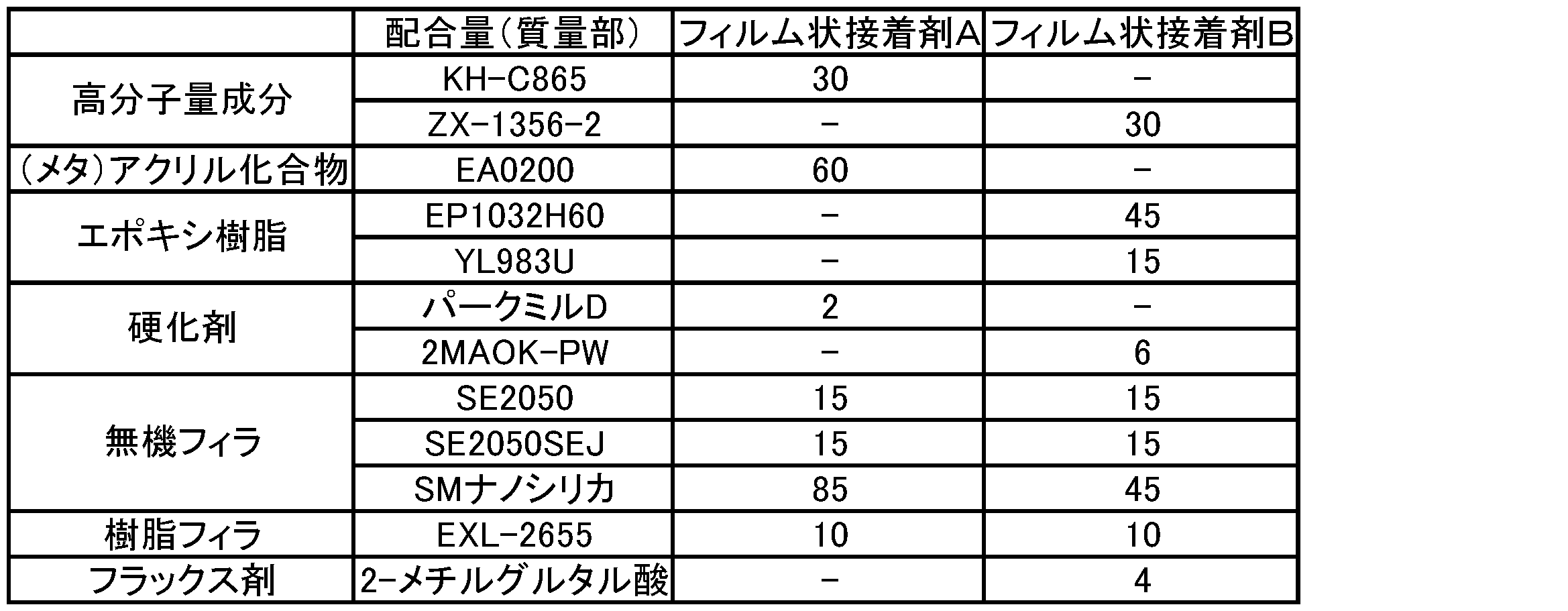
(実施例1)
工程1:上記にて作製したフィルム状接着剤を切り抜き(8mm×8mm×0.045mmt)、基板(20mm×27mm、0.41mm厚、接続部金属:Cu(OSP処理)、製品名:HCTEG-P1180-02、日立化成エレクトロニクス株式会社製)上に貼付した。その上に、はんだバンプ付き半導体チップ(チップサイズ:7.3mm×7.3mm×0.15mmt、バンプ高さ:銅ピラー+はんだ計約45μm、バンプ数328ピン、ピッチ80μm、製品名:SM487A-HC-PLT、住友商事九州株式会社製)を、熱圧着機(FCB3、パナソニック株式会社製)を用いて、ステージ温度80℃、仮圧着温度130℃、仮圧着時間2秒間の条件で仮圧着した。
工程2:仮圧着を行った半導体パッケージ(仮接続体)に対し、モールド装置(株式会社テクノマルチシ製)を用いて、チップ上面の封止を行い、封止体(封止仮接続体)を形成した。
工程3:得られた封止体に対し、上記熱圧着機(FCB3、パナソニック株式会社製)を用いてステージ温度80℃、圧着温度280℃で加熱処理を行い、半導体装置(封止接続体)を作製した。
表2に示すように、加熱処理を熱圧着機(FCB3、パナソニック株式会社製)又はリフロー装置(株式会社タムラ製作所製)を用いて行ったこと、フィルム状接着剤としてフィルム状接着剤A又はBを用いたこと、そして仮圧着温度を130℃(フィルム状接着剤Aを用いた場合)又は80℃(フィルム状接着剤Bを用いた場合)、としたこと以外は、実施例1と同様にして半導体装置を作製した。
表2に示すように、加熱処理を熱圧着機(FCB3、パナソニック株式会社製)又はリフロー装置(株式会社タムラ製作所製)を用いて行ったこと、フィルム状接着剤としてフィルム状接着剤A又はBを用いたこと、工程2と工程3とを入れ替えたこと、そして仮圧着温度を130℃(フィルム状接着剤Aを用いた場合)又は80℃(フィルム状接着剤Bを用いた場合)、としたこと以外は、実施例1と同様にして半導体装置を作製した。なお、工程2と工程3とを入れ替えるとは、基板と半導体チップとの接続が完了した後に、モールド装置を用いて封止処理を行ったということである。
・溶融粘度評価
上記にて作製したフィルム状接着剤に対し、レオメーター(アントンパール ジャパン社製、MCR301)及び治具(ディスポーザブルプレート(直径8mm)とディスポーザブルサンプルディッシュ)を用いて、サンプル厚み400μm、昇温速度10℃/分、周波数1Hz、の条件で、工程1(仮圧着温度:80~130℃)における溶融粘度を測定した。結果を表2に示す。
・反り評価
上記にて作製した各半導体装置に対し、非接触式形状測定装置(SONY製)を用いて、チップの対角方向の2辺の形状を計測した。EXCELを用いて、計測データの傾きを補正し、1辺の凹凸の最大値と最小値の差を反り量(μm)とした。結果を表2に示す。
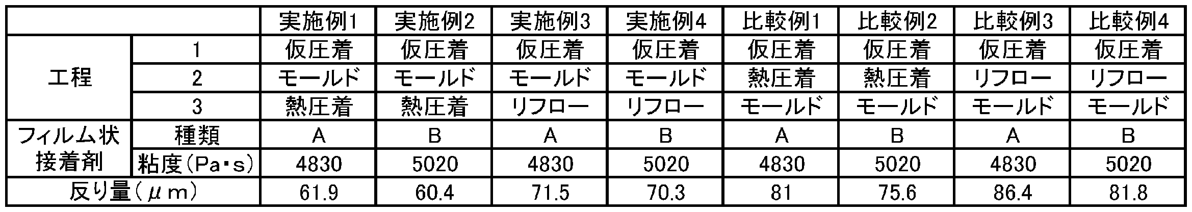
Claims (10)
- 接続部を有する半導体チップ及び接続部を有する配線回路基板を備え、それぞれの前記接続部が互いに電気的に接続された半導体装置、又は、接続部を有する複数の半導体チップを備え、それぞれの前記接続部が互いに電気的に接続された半導体装置の製造方法であって、
前記接続部は金属からなり、
(a)前記半導体チップ及び前記配線回路基板、又は、前記半導体チップ同士を、間に半導体用接着剤を介した状態で、前記接続部の金属の融点より低い温度で、それぞれの前記接続部が互いに接触するように圧着し、仮接続体を得る第一工程と、
(b)前記仮接続体の少なくとも一部を封止用樹脂を用いて封止し、封止仮接続体を得る第二工程と、
(c)前記封止仮接続体を前記接続部の金属の融点以上の温度で加熱し、封止接続体を得る第三工程と、
を備える、半導体装置の製造方法。 - 接続部を有する半導体チップ及び接続部を有する配線回路基板を備え、それぞれの前記接続部が接続バンプを介して互いに電気的に接続された半導体装置、又は、接続部を有する複数の半導体チップを備え、それぞれの前記接続部が接続バンプを介して互いに電気的に接続された半導体装置の製造方法であって、
前記接続部及び前記接続バンプは金属からなり、
(a)前記半導体チップ及び前記配線回路基板、又は、前記半導体チップ同士を、間に半導体用接着剤を介した状態で、前記接続バンプの金属の融点より低い温度で、それぞれの前記接続部が前記接続バンプに接触するように圧着し、仮接続体を得る第一工程と、
(b)前記仮接続体の少なくとも一部を封止用樹脂を用いて封止し、封止仮接続体を得る第二工程と、
(c)前記封止仮接続体を前記接続バンプの金属の融点以上の温度で加熱し、封止接続体を得る第三工程と、
を備える、半導体装置の製造方法。 - 前記第一工程では、前記半導体チップ及び前記配線回路基板、又は、前記半導体チップ同士を、対向する一対の押圧部材で挟むことによって加熱及び加圧することにより、圧着する、請求項1又は2に記載の半導体装置の製造方法。
- 前記半導体用接着剤が、重量平均分子量10000以下の化合物及び硬化剤を含有し、80~130℃における溶融粘度が6000Pa・s以下である、請求項1~3のいずれか一項に記載の半導体装置の製造方法。
- 前記半導体用接着剤が、重量平均分子量10000以下の化合物、硬化剤、及び下記一般式(1)で表されるシラノール化合物を含有する、請求項1~4のいずれか一項に記載の半導体装置の製造方法。

- 前記R1がフェニル基である、請求項5に記載の半導体装置の製造方法。
- 前記シラノール化合物が25℃で固形である、請求項5又は6に記載の半導体装置の製造方法。
- 前記半導体用接着剤が、重量平均分子量10000超の高分子量成分を含有する、請求項1~7のいずれか一項に記載の半導体装置の製造方法。
- 前記高分子量成分が、重量平均分子量30000以上であり且つガラス転移温度が100℃以下の成分である、請求項8に記載の半導体装置の製造方法。
- 前記半導体用接着剤がフィルム状である、請求項1~9のいずれか一項に記載の半導体装置の製造方法。
Priority Applications (5)
| Application Number | Priority Date | Filing Date | Title |
|---|---|---|---|
| SG11201809734RA SG11201809734RA (en) | 2016-05-09 | 2017-04-10 | Method for manufacturing semiconductor device |
| KR1020187031285A KR102190177B1 (ko) | 2016-05-09 | 2017-04-10 | 반도체 장치의 제조 방법 |
| US16/099,753 US10734350B2 (en) | 2016-05-09 | 2017-04-10 | Method for manufacturing semiconductor device |
| JP2018516901A JP6477971B2 (ja) | 2016-05-09 | 2017-04-10 | 半導体装置の製造方法 |
| CN201780028064.4A CN109075088B (zh) | 2016-05-09 | 2017-04-10 | 半导体装置的制造方法 |
Applications Claiming Priority (4)
| Application Number | Priority Date | Filing Date | Title |
|---|---|---|---|
| JP2016-093809 | 2016-05-09 | ||
| JP2016093809 | 2016-05-09 | ||
| JP2016-115355 | 2016-06-09 | ||
| JP2016115355 | 2016-06-09 |
Publications (1)
| Publication Number | Publication Date |
|---|---|
| WO2017195517A1 true WO2017195517A1 (ja) | 2017-11-16 |
Family
ID=60267830
Family Applications (1)
| Application Number | Title | Priority Date | Filing Date |
|---|---|---|---|
| PCT/JP2017/014680 WO2017195517A1 (ja) | 2016-05-09 | 2017-04-10 | 半導体装置の製造方法 |
Country Status (7)
| Country | Link |
|---|---|
| US (1) | US10734350B2 (ja) |
| JP (1) | JP6477971B2 (ja) |
| KR (1) | KR102190177B1 (ja) |
| CN (1) | CN109075088B (ja) |
| SG (1) | SG11201809734RA (ja) |
| TW (1) | TWI721150B (ja) |
| WO (1) | WO2017195517A1 (ja) |
Cited By (2)
| Publication number | Priority date | Publication date | Assignee | Title |
|---|---|---|---|---|
| CN111480218A (zh) * | 2017-12-18 | 2020-07-31 | 日立化成株式会社 | 半导体装置、半导体装置的制造方法和粘接剂 |
| JP2020136398A (ja) * | 2019-02-15 | 2020-08-31 | 日立化成株式会社 | 半導体用接着剤 |
Families Citing this family (4)
| Publication number | Priority date | Publication date | Assignee | Title |
|---|---|---|---|---|
| JP6926018B2 (ja) * | 2018-03-28 | 2021-08-25 | 東レエンジニアリング株式会社 | 転写基板ならびにこれを用いた実装方法および画像表示装置の製造方法 |
| EP4075485A4 (en) * | 2019-12-13 | 2024-04-10 | Connectec America Inc | METHOD FOR MANUFACTURING ELECTRONIC COMPONENTS |
| JP2021129083A (ja) * | 2020-02-17 | 2021-09-02 | キオクシア株式会社 | 半導体装置およびその製造方法 |
| US11769730B2 (en) * | 2020-03-27 | 2023-09-26 | STATS ChipPAC Pte. Ltd. | Semiconductor device and method of providing high density component spacing |
Citations (3)
| Publication number | Priority date | Publication date | Assignee | Title |
|---|---|---|---|---|
| JPH07273147A (ja) * | 1994-04-01 | 1995-10-20 | Nippondenso Co Ltd | 半導体装置の実装方法 |
| JPH10112476A (ja) * | 1996-10-04 | 1998-04-28 | Fuji Xerox Co Ltd | 半導体装置の製造方法 |
| JPH1126511A (ja) * | 1997-07-08 | 1999-01-29 | Matsushita Electric Ind Co Ltd | バンプ付きワークの実装方法 |
Family Cites Families (33)
| Publication number | Priority date | Publication date | Assignee | Title |
|---|---|---|---|---|
| JPH02280349A (ja) | 1989-04-20 | 1990-11-16 | Mitsubishi Electric Corp | バンプの形成方法およびバンプの接続方法 |
| JP2786700B2 (ja) | 1989-11-29 | 1998-08-13 | 株式会社日立製作所 | 半導体集積回路装置の製造方法および製造装置 |
| KR100894208B1 (ko) | 2000-03-31 | 2009-04-22 | 히다치 가세고교 가부시끼가이샤 | 접착제 조성물, 그의 제조 방법, 이것을 사용한 접착 필름,반도체 탑재용 기판 및 반도체 장치 |
| JP3597754B2 (ja) * | 2000-04-24 | 2004-12-08 | Necエレクトロニクス株式会社 | 半導体装置及びその製造方法 |
| JP4024458B2 (ja) * | 2000-06-27 | 2007-12-19 | 株式会社東芝 | 半導体装置の実装方法および半導体装置実装体の製造方法 |
| JP4766831B2 (ja) | 2002-11-26 | 2011-09-07 | 株式会社村田製作所 | 電子部品の製造方法 |
| CN100587930C (zh) * | 2005-05-17 | 2010-02-03 | 松下电器产业株式会社 | 倒装片安装体及倒装片安装方法 |
| US20060292823A1 (en) | 2005-06-28 | 2006-12-28 | Shriram Ramanathan | Method and apparatus for bonding wafers |
| JP4386453B2 (ja) * | 2006-05-31 | 2009-12-16 | 信越化学工業株式会社 | 樹脂封止された半導体装置 |
| JP4589269B2 (ja) * | 2006-06-16 | 2010-12-01 | ソニー株式会社 | 半導体装置およびその製造方法 |
| JP2008109009A (ja) | 2006-10-27 | 2008-05-08 | Sony Corp | 半導体装置の製造方法 |
| JP4305502B2 (ja) * | 2006-11-28 | 2009-07-29 | カシオ計算機株式会社 | 半導体装置の製造方法 |
| JP5217260B2 (ja) | 2007-04-27 | 2013-06-19 | 住友ベークライト株式会社 | 半導体ウエハーの接合方法および半導体装置の製造方法 |
| JP5123341B2 (ja) | 2010-03-15 | 2013-01-23 | 信越化学工業株式会社 | 接着剤組成物、半導体ウエハ保護膜形成用シート |
| KR101763975B1 (ko) * | 2010-05-07 | 2017-08-01 | 스미토모 베이클리트 컴퍼니 리미티드 | 회로 기판용 에폭시 수지 조성물, 프리프레그, 적층판, 수지 시트, 프린트 배선판용 적층기재, 프린트 배선판, 및 반도체 장치 |
| KR101455951B1 (ko) * | 2010-09-30 | 2014-10-28 | 히타치가세이가부시끼가이샤 | 접착제 조성물, 반도체 장치의 제조 방법 및 반도체 장치 |
| JP5344097B2 (ja) * | 2010-11-18 | 2013-11-20 | 日立化成株式会社 | 半導体封止充てん用フィルム状樹脂組成物、半導体装置の製造方法及び半導体装置 |
| JP5866851B2 (ja) * | 2011-08-05 | 2016-02-24 | 日立化成株式会社 | 半導体装置の製造方法、フィルム状接着剤及び接着剤シート |
| JP2013065835A (ja) * | 2011-08-24 | 2013-04-11 | Sumitomo Bakelite Co Ltd | 半導体装置の製造方法、ブロック積層体及び逐次積層体 |
| TW201330217A (zh) | 2011-11-11 | 2013-07-16 | Sumitomo Bakelite Co | 半導體裝置之製造方法 |
| WO2013108890A1 (ja) * | 2012-01-20 | 2013-07-25 | 旭化成イーマテリアルズ株式会社 | 樹脂組成物、積層体、多層プリント配線板及び多層フレキシブル配線板並びにその製造方法 |
| JP6209313B2 (ja) * | 2012-02-20 | 2017-10-04 | デクセリアルズ株式会社 | 異方性導電フィルム、接続構造体、接続構造体の製造方法及び接続方法 |
| JP6047888B2 (ja) | 2012-02-24 | 2016-12-21 | 日立化成株式会社 | 半導体用接着剤及び半導体装置の製造方法 |
| CN104137246A (zh) * | 2012-02-24 | 2014-11-05 | 日立化成株式会社 | 半导体装置及其制造方法 |
| KR20140140042A (ko) | 2012-03-07 | 2014-12-08 | 도레이 카부시키가이샤 | 반도체 장치의 제조 방법 및 반도체 장치의 제조 장치 |
| JP5990940B2 (ja) | 2012-03-09 | 2016-09-14 | 日立化成株式会社 | 回路接続構造体の製造方法 |
| JP2014143316A (ja) | 2013-01-24 | 2014-08-07 | Sanyu Rec Co Ltd | フリップチップ部品の樹脂封止方法 |
| KR20160030527A (ko) * | 2013-07-11 | 2016-03-18 | 스미또모 베이크라이트 가부시키가이샤 | 반도체 장치의 제조 방법 및 반도체 장치 |
| WO2015186744A1 (ja) * | 2014-06-04 | 2015-12-10 | 日立化成株式会社 | フィルム状エポキシ樹脂組成物、フィルム状エポキシ樹脂組成物の製造方法、及び半導体装置の製造方法 |
| JP2016046299A (ja) * | 2014-08-20 | 2016-04-04 | 日立化成株式会社 | 半導体接続部封止用接着剤及びこれを用いた半導体装置、半導体装置の製造方法 |
| JP2016058655A (ja) * | 2014-09-11 | 2016-04-21 | 株式会社ジェイデバイス | 半導体装置の製造方法 |
| WO2016158935A1 (ja) | 2015-03-30 | 2016-10-06 | 東レエンジニアリング株式会社 | 半導体装置の製造方法、半導体実装装置および半導体装置の製造方法で製造されたメモリデバイス |
| JP6504263B2 (ja) * | 2015-10-29 | 2019-04-24 | 日立化成株式会社 | 半導体用接着剤、半導体装置及びそれを製造する方法 |
-
2017
- 2017-04-10 CN CN201780028064.4A patent/CN109075088B/zh active Active
- 2017-04-10 JP JP2018516901A patent/JP6477971B2/ja active Active
- 2017-04-10 US US16/099,753 patent/US10734350B2/en active Active
- 2017-04-10 WO PCT/JP2017/014680 patent/WO2017195517A1/ja active Application Filing
- 2017-04-10 KR KR1020187031285A patent/KR102190177B1/ko active IP Right Grant
- 2017-04-10 SG SG11201809734RA patent/SG11201809734RA/en unknown
- 2017-04-12 TW TW106112128A patent/TWI721150B/zh active
Patent Citations (3)
| Publication number | Priority date | Publication date | Assignee | Title |
|---|---|---|---|---|
| JPH07273147A (ja) * | 1994-04-01 | 1995-10-20 | Nippondenso Co Ltd | 半導体装置の実装方法 |
| JPH10112476A (ja) * | 1996-10-04 | 1998-04-28 | Fuji Xerox Co Ltd | 半導体装置の製造方法 |
| JPH1126511A (ja) * | 1997-07-08 | 1999-01-29 | Matsushita Electric Ind Co Ltd | バンプ付きワークの実装方法 |
Cited By (4)
| Publication number | Priority date | Publication date | Assignee | Title |
|---|---|---|---|---|
| CN111480218A (zh) * | 2017-12-18 | 2020-07-31 | 日立化成株式会社 | 半导体装置、半导体装置的制造方法和粘接剂 |
| CN111480218B (zh) * | 2017-12-18 | 2023-07-21 | 株式会社力森诺科 | 半导体装置、半导体装置的制造方法和粘接剂 |
| JP2020136398A (ja) * | 2019-02-15 | 2020-08-31 | 日立化成株式会社 | 半導体用接着剤 |
| JP7238453B2 (ja) | 2019-02-15 | 2023-03-14 | 株式会社レゾナック | 半導体用接着剤 |
Also Published As
| Publication number | Publication date |
|---|---|
| CN109075088A (zh) | 2018-12-21 |
| JP6477971B2 (ja) | 2019-03-06 |
| KR102190177B1 (ko) | 2020-12-11 |
| TWI721150B (zh) | 2021-03-11 |
| CN109075088B (zh) | 2022-01-07 |
| JPWO2017195517A1 (ja) | 2018-11-22 |
| SG11201809734RA (en) | 2018-12-28 |
| US10734350B2 (en) | 2020-08-04 |
| KR20180128958A (ko) | 2018-12-04 |
| US20190123014A1 (en) | 2019-04-25 |
| TW201806044A (zh) | 2018-02-16 |
Similar Documents
| Publication | Publication Date | Title |
|---|---|---|
| KR102064584B1 (ko) | 반도체용 접착제, 반도체 장치 및 그것을 제조하는 방법 | |
| JP6477971B2 (ja) | 半導体装置の製造方法 | |
| JP2017220519A (ja) | 半導体装置の製造方法 | |
| JP2017045891A (ja) | 半導体装置及びそれを製造する方法 | |
| JP2019137866A (ja) | 半導体用接着剤、並びに、半導体装置及びその製造方法 | |
| JP2024023787A (ja) | 半導体装置の製造方法 | |
| KR102455212B1 (ko) | 반도체 장치, 반도체 장치의 제조 방법 및 접착제 | |
| JP2017122193A (ja) | 半導体用接着剤及び半導体装置の製造方法 | |
| JP6859708B2 (ja) | 半導体装置を製造する方法 | |
| JP6544146B2 (ja) | 半導体装置及びそれを製造する方法 | |
| TWI820200B (zh) | 半導體裝置及其製造方法 | |
| JP2017171817A (ja) | 半導体用接着剤、半導体装置、及び半導体装置の製造方法 | |
| JP6690308B2 (ja) | 半導体装置を製造する方法 | |
| JP2021024963A (ja) | 半導体用接着剤、それを用いた半導体用接着剤フィルムの製造方法及び半導体装置の製造方法 | |
| JP2017041499A (ja) | 半導体用接着剤、並びに、半導体装置及びその製造方法 | |
| JP2017218532A (ja) | 半導体用接着剤、半導体装置、及び半導体装置の製造方法 | |
| JP2022043572A (ja) | 半導体装置の製造方法 | |
| JP7238453B2 (ja) | 半導体用接着剤 | |
| JP2017103289A (ja) | 半導体用接着剤、半導体装置、及び半導体装置の製造方法 | |
| WO2020110785A1 (ja) | 半導体用フィルム状接着剤、半導体装置及びその製造方法 | |
| JP2017103304A (ja) | 半導体用接着剤、半導体装置、及び半導体装置の製造方法 | |
| JP2017103303A (ja) | 半導体用接着剤、半導体装置、及び半導体装置の製造方法 |
Legal Events
| Date | Code | Title | Description |
|---|---|---|---|
| WWE | Wipo information: entry into national phase |
Ref document number: 2018516901 Country of ref document: JP |
|
| ENP | Entry into the national phase |
Ref document number: 20187031285 Country of ref document: KR Kind code of ref document: A |
|
| NENP | Non-entry into the national phase |
Ref country code: DE |
|
| 121 | Ep: the epo has been informed by wipo that ep was designated in this application |
Ref document number: 17795878 Country of ref document: EP Kind code of ref document: A1 |
|
| 122 | Ep: pct application non-entry in european phase |
Ref document number: 17795878 Country of ref document: EP Kind code of ref document: A1 |