WO2017170128A1 - パターン形成方法、加工基板の製造方法、光学部品の製造方法、回路基板の製造方法、電子部品の製造方法、インプリントモールドの製造方法 - Google Patents
パターン形成方法、加工基板の製造方法、光学部品の製造方法、回路基板の製造方法、電子部品の製造方法、インプリントモールドの製造方法 Download PDFInfo
- Publication number
- WO2017170128A1 WO2017170128A1 PCT/JP2017/011736 JP2017011736W WO2017170128A1 WO 2017170128 A1 WO2017170128 A1 WO 2017170128A1 JP 2017011736 W JP2017011736 W JP 2017011736W WO 2017170128 A1 WO2017170128 A1 WO 2017170128A1
- Authority
- WO
- WIPO (PCT)
- Prior art keywords
- curable composition
- mold
- component
- substrate
- mpa
- Prior art date
- Legal status (The legal status is an assumption and is not a legal conclusion. Google has not performed a legal analysis and makes no representation as to the accuracy of the status listed.)
- Ceased
Links
Images


Classifications
-
- G—PHYSICS
- G03—PHOTOGRAPHY; CINEMATOGRAPHY; ANALOGOUS TECHNIQUES USING WAVES OTHER THAN OPTICAL WAVES; ELECTROGRAPHY; HOLOGRAPHY
- G03F—PHOTOMECHANICAL PRODUCTION OF TEXTURED OR PATTERNED SURFACES, e.g. FOR PRINTING, FOR PROCESSING OF SEMICONDUCTOR DEVICES; MATERIALS THEREFOR; ORIGINALS THEREFOR; APPARATUS SPECIALLY ADAPTED THEREFOR
- G03F7/00—Photomechanical, e.g. photolithographic, production of textured or patterned surfaces, e.g. printing surfaces; Materials therefor, e.g. comprising photoresists; Apparatus specially adapted therefor
- G03F7/0002—Lithographic processes using patterning methods other than those involving the exposure to radiation, e.g. by stamping
-
- C—CHEMISTRY; METALLURGY
- C09—DYES; PAINTS; POLISHES; NATURAL RESINS; ADHESIVES; COMPOSITIONS NOT OTHERWISE PROVIDED FOR; APPLICATIONS OF MATERIALS NOT OTHERWISE PROVIDED FOR
- C09D—COATING COMPOSITIONS, e.g. PAINTS, VARNISHES OR LACQUERS; FILLING PASTES; CHEMICAL PAINT OR INK REMOVERS; INKS; CORRECTING FLUIDS; WOODSTAINS; PASTES OR SOLIDS FOR COLOURING OR PRINTING; USE OF MATERIALS THEREFOR
- C09D11/00—Inks
- C09D11/02—Printing inks
- C09D11/10—Printing inks based on artificial resins
- C09D11/101—Inks specially adapted for printing processes involving curing by wave energy or particle radiation, e.g. with UV-curing following the printing
-
- B—PERFORMING OPERATIONS; TRANSPORTING
- B05—SPRAYING OR ATOMISING IN GENERAL; APPLYING FLUENT MATERIALS TO SURFACES, IN GENERAL
- B05D—PROCESSES FOR APPLYING FLUENT MATERIALS TO SURFACES, IN GENERAL
- B05D1/00—Processes for applying liquids or other fluent materials
- B05D1/30—Processes for applying liquids or other fluent materials performed by gravity only, i.e. flow coating
-
- B—PERFORMING OPERATIONS; TRANSPORTING
- B05—SPRAYING OR ATOMISING IN GENERAL; APPLYING FLUENT MATERIALS TO SURFACES, IN GENERAL
- B05D—PROCESSES FOR APPLYING FLUENT MATERIALS TO SURFACES, IN GENERAL
- B05D3/00—Pretreatment of surfaces to which liquids or other fluent materials are to be applied; After-treatment of applied coatings, e.g. intermediate treating of an applied coating preparatory to subsequent applications of liquids or other fluent materials
- B05D3/04—Pretreatment of surfaces to which liquids or other fluent materials are to be applied; After-treatment of applied coatings, e.g. intermediate treating of an applied coating preparatory to subsequent applications of liquids or other fluent materials by exposure to gases
-
- B—PERFORMING OPERATIONS; TRANSPORTING
- B05—SPRAYING OR ATOMISING IN GENERAL; APPLYING FLUENT MATERIALS TO SURFACES, IN GENERAL
- B05D—PROCESSES FOR APPLYING FLUENT MATERIALS TO SURFACES, IN GENERAL
- B05D3/00—Pretreatment of surfaces to which liquids or other fluent materials are to be applied; After-treatment of applied coatings, e.g. intermediate treating of an applied coating preparatory to subsequent applications of liquids or other fluent materials
- B05D3/12—Pretreatment of surfaces to which liquids or other fluent materials are to be applied; After-treatment of applied coatings, e.g. intermediate treating of an applied coating preparatory to subsequent applications of liquids or other fluent materials by mechanical means
-
- B—PERFORMING OPERATIONS; TRANSPORTING
- B29—WORKING OF PLASTICS; WORKING OF SUBSTANCES IN A PLASTIC STATE IN GENERAL
- B29C—SHAPING OR JOINING OF PLASTICS; SHAPING OF MATERIAL IN A PLASTIC STATE, NOT OTHERWISE PROVIDED FOR; AFTER-TREATMENT OF THE SHAPED PRODUCTS, e.g. REPAIRING
- B29C35/00—Heating, cooling or curing, e.g. crosslinking or vulcanising; Apparatus therefor
- B29C35/02—Heating or curing, e.g. crosslinking or vulcanizing during moulding, e.g. in a mould
- B29C35/08—Heating or curing, e.g. crosslinking or vulcanizing during moulding, e.g. in a mould by wave energy or particle radiation
- B29C35/0805—Heating or curing, e.g. crosslinking or vulcanizing during moulding, e.g. in a mould by wave energy or particle radiation using electromagnetic radiation
-
- B—PERFORMING OPERATIONS; TRANSPORTING
- B29—WORKING OF PLASTICS; WORKING OF SUBSTANCES IN A PLASTIC STATE IN GENERAL
- B29C—SHAPING OR JOINING OF PLASTICS; SHAPING OF MATERIAL IN A PLASTIC STATE, NOT OTHERWISE PROVIDED FOR; AFTER-TREATMENT OF THE SHAPED PRODUCTS, e.g. REPAIRING
- B29C59/00—Surface shaping of articles, e.g. embossing; Apparatus therefor
- B29C59/02—Surface shaping of articles, e.g. embossing; Apparatus therefor by mechanical means, e.g. pressing
- B29C59/026—Surface shaping of articles, e.g. embossing; Apparatus therefor by mechanical means, e.g. pressing of layered or coated substantially flat surfaces
-
- C—CHEMISTRY; METALLURGY
- C09—DYES; PAINTS; POLISHES; NATURAL RESINS; ADHESIVES; COMPOSITIONS NOT OTHERWISE PROVIDED FOR; APPLICATIONS OF MATERIALS NOT OTHERWISE PROVIDED FOR
- C09D—COATING COMPOSITIONS, e.g. PAINTS, VARNISHES OR LACQUERS; FILLING PASTES; CHEMICAL PAINT OR INK REMOVERS; INKS; CORRECTING FLUIDS; WOODSTAINS; PASTES OR SOLIDS FOR COLOURING OR PRINTING; USE OF MATERIALS THEREFOR
- C09D11/00—Inks
- C09D11/02—Printing inks
- C09D11/10—Printing inks based on artificial resins
- C09D11/106—Printing inks based on artificial resins containing macromolecular compounds obtained by reactions only involving carbon-to-carbon unsaturated bonds
- C09D11/107—Printing inks based on artificial resins containing macromolecular compounds obtained by reactions only involving carbon-to-carbon unsaturated bonds from unsaturated acids or derivatives thereof
-
- C—CHEMISTRY; METALLURGY
- C09—DYES; PAINTS; POLISHES; NATURAL RESINS; ADHESIVES; COMPOSITIONS NOT OTHERWISE PROVIDED FOR; APPLICATIONS OF MATERIALS NOT OTHERWISE PROVIDED FOR
- C09D—COATING COMPOSITIONS, e.g. PAINTS, VARNISHES OR LACQUERS; FILLING PASTES; CHEMICAL PAINT OR INK REMOVERS; INKS; CORRECTING FLUIDS; WOODSTAINS; PASTES OR SOLIDS FOR COLOURING OR PRINTING; USE OF MATERIALS THEREFOR
- C09D11/00—Inks
- C09D11/30—Inkjet printing inks
-
- C—CHEMISTRY; METALLURGY
- C09—DYES; PAINTS; POLISHES; NATURAL RESINS; ADHESIVES; COMPOSITIONS NOT OTHERWISE PROVIDED FOR; APPLICATIONS OF MATERIALS NOT OTHERWISE PROVIDED FOR
- C09D—COATING COMPOSITIONS, e.g. PAINTS, VARNISHES OR LACQUERS; FILLING PASTES; CHEMICAL PAINT OR INK REMOVERS; INKS; CORRECTING FLUIDS; WOODSTAINS; PASTES OR SOLIDS FOR COLOURING OR PRINTING; USE OF MATERIALS THEREFOR
- C09D133/00—Coating compositions based on homopolymers or copolymers of compounds having one or more unsaturated aliphatic radicals, each having only one carbon-to-carbon double bond, and at least one being terminated by only one carboxyl radical, or of salts, anhydrides, esters, amides, imides, or nitriles thereof; Coating compositions based on derivatives of such polymers
- C09D133/04—Homopolymers or copolymers of esters
- C09D133/06—Homopolymers or copolymers of esters of esters containing only carbon, hydrogen and oxygen, the oxygen atom being present only as part of the carboxyl radical
-
- C—CHEMISTRY; METALLURGY
- C09—DYES; PAINTS; POLISHES; NATURAL RESINS; ADHESIVES; COMPOSITIONS NOT OTHERWISE PROVIDED FOR; APPLICATIONS OF MATERIALS NOT OTHERWISE PROVIDED FOR
- C09D—COATING COMPOSITIONS, e.g. PAINTS, VARNISHES OR LACQUERS; FILLING PASTES; CHEMICAL PAINT OR INK REMOVERS; INKS; CORRECTING FLUIDS; WOODSTAINS; PASTES OR SOLIDS FOR COLOURING OR PRINTING; USE OF MATERIALS THEREFOR
- C09D133/00—Coating compositions based on homopolymers or copolymers of compounds having one or more unsaturated aliphatic radicals, each having only one carbon-to-carbon double bond, and at least one being terminated by only one carboxyl radical, or of salts, anhydrides, esters, amides, imides, or nitriles thereof; Coating compositions based on derivatives of such polymers
- C09D133/04—Homopolymers or copolymers of esters
- C09D133/06—Homopolymers or copolymers of esters of esters containing only carbon, hydrogen and oxygen, the oxygen atom being present only as part of the carboxyl radical
- C09D133/08—Homopolymers or copolymers of acrylic acid esters
-
- C—CHEMISTRY; METALLURGY
- C09—DYES; PAINTS; POLISHES; NATURAL RESINS; ADHESIVES; COMPOSITIONS NOT OTHERWISE PROVIDED FOR; APPLICATIONS OF MATERIALS NOT OTHERWISE PROVIDED FOR
- C09D—COATING COMPOSITIONS, e.g. PAINTS, VARNISHES OR LACQUERS; FILLING PASTES; CHEMICAL PAINT OR INK REMOVERS; INKS; CORRECTING FLUIDS; WOODSTAINS; PASTES OR SOLIDS FOR COLOURING OR PRINTING; USE OF MATERIALS THEREFOR
- C09D135/00—Coating compositions based on homopolymers or copolymers of compounds having one or more unsaturated aliphatic radicals, each having only one carbon-to-carbon double bond, and at least one being terminated by a carboxyl radical, and containing at least another carboxyl radical in the molecule, or of salts, anhydrides, esters, amides, imides or nitriles thereof; Coating compositions based on derivatives of such polymers
- C09D135/02—Homopolymers or copolymers of esters
-
- G—PHYSICS
- G03—PHOTOGRAPHY; CINEMATOGRAPHY; ANALOGOUS TECHNIQUES USING WAVES OTHER THAN OPTICAL WAVES; ELECTROGRAPHY; HOLOGRAPHY
- G03F—PHOTOMECHANICAL PRODUCTION OF TEXTURED OR PATTERNED SURFACES, e.g. FOR PRINTING, FOR PROCESSING OF SEMICONDUCTOR DEVICES; MATERIALS THEREFOR; ORIGINALS THEREFOR; APPARATUS SPECIALLY ADAPTED THEREFOR
- G03F7/00—Photomechanical, e.g. photolithographic, production of textured or patterned surfaces, e.g. printing surfaces; Materials therefor, e.g. comprising photoresists; Apparatus specially adapted therefor
- G03F7/16—Coating processes; Apparatus therefor
- G03F7/161—Coating processes; Apparatus therefor using a previously coated surface, e.g. by stamping or by transfer lamination
-
- B—PERFORMING OPERATIONS; TRANSPORTING
- B29—WORKING OF PLASTICS; WORKING OF SUBSTANCES IN A PLASTIC STATE IN GENERAL
- B29C—SHAPING OR JOINING OF PLASTICS; SHAPING OF MATERIAL IN A PLASTIC STATE, NOT OTHERWISE PROVIDED FOR; AFTER-TREATMENT OF THE SHAPED PRODUCTS, e.g. REPAIRING
- B29C35/00—Heating, cooling or curing, e.g. crosslinking or vulcanising; Apparatus therefor
- B29C35/02—Heating or curing, e.g. crosslinking or vulcanizing during moulding, e.g. in a mould
- B29C35/08—Heating or curing, e.g. crosslinking or vulcanizing during moulding, e.g. in a mould by wave energy or particle radiation
- B29C35/0805—Heating or curing, e.g. crosslinking or vulcanizing during moulding, e.g. in a mould by wave energy or particle radiation using electromagnetic radiation
- B29C2035/0833—Heating or curing, e.g. crosslinking or vulcanizing during moulding, e.g. in a mould by wave energy or particle radiation using electromagnetic radiation using actinic light
-
- B—PERFORMING OPERATIONS; TRANSPORTING
- B29—WORKING OF PLASTICS; WORKING OF SUBSTANCES IN A PLASTIC STATE IN GENERAL
- B29K—INDEXING SCHEME ASSOCIATED WITH SUBCLASSES B29B, B29C OR B29D, RELATING TO MOULDING MATERIALS OR TO MATERIALS FOR MOULDS, REINFORCEMENTS, FILLERS OR PREFORMED PARTS, e.g. INSERTS
- B29K2033/00—Use of polymers of unsaturated acids or derivatives thereof as moulding material
- B29K2033/04—Polymers of esters
- B29K2033/08—Polymers of acrylic acid esters, e.g. PMA, i.e. polymethylacrylate
-
- B—PERFORMING OPERATIONS; TRANSPORTING
- B29—WORKING OF PLASTICS; WORKING OF SUBSTANCES IN A PLASTIC STATE IN GENERAL
- B29L—INDEXING SCHEME ASSOCIATED WITH SUBCLASS B29C, RELATING TO PARTICULAR ARTICLES
- B29L2011/00—Optical elements, e.g. lenses, prisms
-
- B—PERFORMING OPERATIONS; TRANSPORTING
- B29—WORKING OF PLASTICS; WORKING OF SUBSTANCES IN A PLASTIC STATE IN GENERAL
- B29L—INDEXING SCHEME ASSOCIATED WITH SUBCLASS B29C, RELATING TO PARTICULAR ARTICLES
- B29L2031/00—Other particular articles
- B29L2031/34—Electrical apparatus, e.g. sparking plugs or parts thereof
Definitions
- the present invention relates to a pattern forming method, a processed substrate manufacturing method, an optical component manufacturing method, a circuit board manufacturing method, an electronic component manufacturing method, and an imprint mold manufacturing method.
- the photocurable composition is cured in a state where a mold (mold) having a fine uneven pattern formed on the surface is pressed against a substrate (wafer) coated with the photocurable composition (resist).
- corrugated pattern of a mold is transcribe
- a fine structure of the order of several nanometers can be formed on a substrate.
- the liquid resist 102 is discretely dropped onto the pattern formation region on the substrate 101 by using an inkjet method (arrangement step (1), FIGS. 1A and 1B).
- the dropped resist droplet spreads on the substrate as indicated by an arrow 104, and this phenomenon is called pre-spread (FIG. 1C).
- this resist is molded using a mold (mold) 105 having a pattern and transparent to irradiation light described later (mold contact step (2), FIG. 1D).
- the resist droplet spreads over the entire gap between the substrate and the mold as indicated by an arrow 104 by capillary action (partially enlarged portion in FIG. 1D). This phenomenon is called spread.
- the resist is filled into the recesses on the mold by capillary action as indicated by an arrow 104 (partially enlarged portion in FIG. 1D). This filling phenomenon is called fill. The time until the spread and fill are completed is called the filling time.
- the resist is cured by irradiating with light 106 (light irradiation step (3), FIG. 1E), and then the substrate is separated from the mold (release step (4), FIG. 1F). By performing these steps, a photocured film 107 (FIG. 1F) having a predetermined pattern shape is formed on the substrate.
- the resist is not formed as a uniform film in advance on the substrate before introduction of the imprint apparatus, but by disposing the resist discretely in the imprint apparatus according to the density of the desired pattern, A finer pattern with higher accuracy can be formed.
- SST-NIL short spread time nanoimprint technology
- a first lamination step (1) for uniformly laminating a liquid curable composition (A1) 202 on a substrate 201
- Second imprinting step (2) for discretely laminating droplets of curable composition (A2) 203 on the layer of curable composition (A1) 202 in the imprint apparatus (FIGS. 2C and 2D).
- a mold contact step (3) (FIG.
- a light irradiation step (4) (FIG. 2F) for curing the mixed layer formed by partially mixing the two curable compositions by irradiating light from the outside of the mold;
- a mold release step (5) (FIG. 2G) for separating the mold 205 from the layer (cured film 207 having a pattern shape) made of the curable composition after curing;
- shot a series of process units from the second lamination process (2) to the mold release process (5) is referred to as “shot”, and the area where the mold contacts the curable compositions (A1) and (A2), That is, a region where a pattern is formed on the substrate is referred to as a “shot region”.
- the lamination process of the curable composition (A1) is performed outside the imprint apparatus or in another chamber inside the imprint apparatus, the throughput of the imprint apparatus is not affected.
- step (2) the second composition is discretely arranged on the first composition layer, which is uniformly laminated in advance outside the imprint apparatus, according to the pattern density using an inkjet method.
- SST-NIL is a new method of optical nanoimprinting that achieves both high-precision pattern accuracy and high-throughput performance using two types of curable compositions.
- the curable composition (A1) 302 is laminated on the substrate 301 over a region wider than the desired (first) shot region 304, for example, the entire surface of the substrate using, for example, a spin coating method.
- the curable composition (A2) 303 is limited to the shot region 304 and is laminated discretely using, for example, an inkjet method (step (1), FIG. 3A).
- the mold 308 and the shot region 304 on the substrate 301 are brought close to each other, and the space between them is replaced with an atmosphere control gas 307 such as helium or nitrogen to expel oxygen, moisture, or the like that inhibits curing.
- an atmosphere control gas 307 such as helium or nitrogen to expel oxygen, moisture, or the like that inhibits curing.
- inert gas such as nitrogen, carbon dioxide, helium, argon, and various chlorofluorocarbons that prevent oxygen inhibition, but also H 2 having a small molecule that easily penetrates an object from a confined space is used. Also good. Furthermore, a condensable gas (such as 1,1,1,3,3-pentafluoropropane) may be used (step (2), FIG. 3B).
- a change in film thickness or composition of the curable composition (A1) due to the air flow of the atmosphere control gas may occur (step (3) ), FIG. 3C).
- step (3) a change in film thickness or composition of the curable composition due to the air flow of the atmosphere control gas
- step (3) a change in film thickness or composition of the curable composition due to the air flow of the atmosphere control gas
- region 309 becomes slow (process (4), FIG. 3D).
- the inventors of the present invention have a slow expansion of some of the droplets, which causes an unfilled defect in the second shot region 305, or a longer filling time in order to prevent the unfilled defect from occurring. As a result, they found a problem that productivity was lowered.
- An object of the present invention is to provide an SST-NIL technology that can process a plurality of shot regions of a substrate with uniform accuracy with high throughput and low cost.
- the method for forming a cured product according to the present invention includes a first laminating step (1) for laminating a layer made of a curable composition (A1) containing at least a polymerizable compound (a1) on the surface of a substrate, A second laminating step (2) for laminating droplets of the curable composition (A2) containing at least the polymerizable compound (a2) discretely on the layer made of the curable composition (A1); A mold contact step (3) in which a mixed layer formed by partially mixing the curable composition (A1) and the curable composition (A2) is sandwiched between a mold and the substrate; A light irradiation step (4) for curing the mixed layer by irradiating light from the mold side; A mold release step (5) for separating the mold from the mixed layer after curing; In the order described above, The viscosity at 25 ° C.
- the viscosity at 25 ° C. of the curable composition (A2) excluding the solvent is 1 mPa ⁇ s or more and less than 40 mPa ⁇ s, and the curable composition (A2) is discretely arranged in the second lamination step (2). Droplets are formed, It is characterized by that.
- a pattern forming method capable of processing a plurality of shot regions of a substrate with uniform accuracy with high throughput and low cost.
- FIG. 5 is a schematic cross-sectional view illustrating a step of disposing droplets of the curable composition (A2) on the liquid film of the curable composition (A1) in the SST-NIL technique.
- Schematic cross section for explaining the step of irradiating light by sandwiching a mixed layer formed by partially mixing the curable composition (A1) and the curable composition (A2) between the mold and the substrate in the SST-NIL technology
- FIG. 5 is a schematic cross-sectional view for explaining changes that occur in the film thickness and composition of the curable composition (A1) in the peripheral shot region in the SST-NIL technique.
- FIG. 6 is a schematic cross-sectional view for explaining that the expansion of droplets in a peripheral shot region is delayed in the SST-NIL technique. It is a schematic diagram which shows collection of the volatile component of the liquid film in one form of invention.
- the curable compositions (A1) and (A2) according to this embodiment are compounds having at least a component (a) that is a polymerizable compound.
- the curable composition according to this embodiment may further contain a component (b) that is a photopolymerization initiator, a non-polymerizable compound (c), and a component (d) that is a solvent.
- the cured film means a film obtained by polymerizing a curable composition on a substrate and curing it.
- shape of a cured film is not specifically limited, You may have a pattern shape on the surface.
- Component (a) is a polymerizable compound.
- the polymerizable compound means a film made of a polymer compound by reacting with a polymerization factor (radical or the like) generated from a photopolymerization initiator (component (b)) and by a chain reaction (polymerization reaction). It is a compound that forms.
- polymerizable compounds examples include radical polymerizable compounds.
- the polymerizable compound as component (a) may be composed of only one type of polymerizable compound or may be composed of a plurality of types of polymerizable compounds.
- the radical polymerizable compound is preferably a compound having at least one acryloyl group or methacryloyl group, that is, a (meth) acrylic compound. Therefore, the curable composition according to the present embodiment preferably includes a (meth) acrylic compound as the component (a), more preferably the main component of the component (a) is a (meth) acrylic compound, Most preferably, all of (a) are (meth) acrylic compounds. In addition, that the main component of the component (a) described here is a (meth) acrylic compound indicates that 90% by weight or more of the component (a) is a (meth) acrylic compound.
- the radically polymerizable compound is composed of a plurality of types of compounds having one or more acryloyl groups or methacryloyl groups, it is preferable to include a monofunctional (meth) acryl monomer and a polyfunctional (meth) acryl monomer. This is because a cured film having high mechanical strength can be obtained by combining a monofunctional (meth) acrylic monomer and a polyfunctional (meth) acrylic monomer.
- Examples of monofunctional (meth) acrylic compounds having one acryloyl group or methacryloyl group include phenoxyethyl (meth) acrylate, phenoxy-2-methylethyl (meth) acrylate, phenoxyethoxyethyl (meth) acrylate, and 3-phenoxy.
- Examples of the polyfunctional (meth) acrylic compound having two or more acryloyl groups or methacryloyl groups include trimethylolpropane di (meth) acrylate, trimethylolpropane tri (meth) acrylate, and EO-modified trimethylolpropane tri (meth) ) Acrylate, PO-modified trimethylolpropane tri (meth) acrylate, EO, PO-modified trimethylolpropane tri (meth) acrylate, dimethyloltricyclodecane di (meth) acrylate, pentaerythritol tri (meth) acrylate, pentaerythritol tetra ( (Meth) acrylate, ethylene glycol di (meth) acrylate, tetraethylene glycol di (meth) acrylate, polyethylene glycol di (meth) acrylate, polypropylene Glycol di (meth) acrylate, 1,4-butanedi
- UV SA1002 As a commercial item of the said polyfunctional (meth) acryl compound, Iupimer (trademark) UV SA1002, SA2007 (above, Mitsubishi Chemical make), Biscote # 195, # 230, # 215, # 260, # 335HP, # 295, # 300, # 360, # 700, GPT, 3PA (above, manufactured by Osaka Organic Chemical Industry), Light Acrylate 4EG-A, 9EG-A, NP-A, DCP-A, BP-4EA, BP-4PA, TMP- A, PE-3A, PE-4A, DPE-6A (manufactured by Kyoeisha Chemical), KAYARAD (registered trademark) PET-30, TMPTA, R-604, DPHA, DPCA-20, -30, -60, -120 HX-620, D-310, D-330 (Nippon Kayaku Co., Ltd.), Aronix (registered trademark) M208, M210, M215 M220, M240, M305,
- (meth) acrylate means acrylate or methacrylate having an alcohol residue equivalent thereto.
- the (meth) acryloyl group means an acryloyl group or a methacryloyl group having an alcohol residue equivalent thereto.
- EO represents ethylene oxide
- EO-modified compound A refers to a compound in which the (meth) acrylic acid residue and alcohol residue of compound A are bonded via a block structure of an ethylene oxide group.
- PO represents propylene oxide
- PO-modified compound B refers to a compound in which the (meth) acrylic acid residue and alcohol residue of compound B are bonded via a block structure of a propylene oxide group.
- Examples of the polymerizable compound (a) used for the curable composition (A1) include trimethylolpropane triacrylate (manufactured by Aldrich), dimethyloltricyclodecane diacrylate (manufactured by Kyoeisha), 1,3-adamantane dimethanol diacrylate ( Idemitsu Kosan Co., Ltd., trimethylolpropane EO 3.5 mol adduct, triacrylate (Idemitsu Kosan), poly (ethylene glycol) diacrylate (Aldrich), 2-hydroxy-3-phenoxypropyl acrylate (Osaka Organic Chemical Co., Ltd., Noni Phenol EO adduct acrylate (manufactured by Kyoeisha), 2-acryloyloxyethyl-succinic acid (manufactured by Kyoeisha), 2-hydroxy-3-acryloyloxypropyl acrylate (manufactured by Kyoeisha), polyethylene glycol #
- the polymerizable compound (a) used for the curable composition (A2) includes isobornyl acrylate (manufactured by Kyoeisha Chemical), benzyl acrylate (manufactured by Osaka Organic Chemical Industry), neopentyl glycol diacrylate (manufactured by Kyoeisha Chemical) (2 -Methyl-2-ethyl-1,3-dioxolan-4-yl) methyl acrylate (manufactured by Osaka Organic Chemical), 1,6-hexanediol diacrylate (manufactured by Shin-Nakamura Chemical Co., Ltd.), 1,9-nonanediol di Acrylate (manufactured by Shin-Nakamura Chemical) 1,10-decanediol diacrylate (manufactured by Shin-Nakamura Chemical), 2-methyl-2-adamantyl acrylate (manufactured by Osaka Organic Chemical), 2-eth
- Component (b) is a photopolymerization initiator.
- the photopolymerization initiator is a compound that senses light of a predetermined wavelength and generates the polymerization factor (radical).
- the photopolymerization initiator is a polymerization initiator (radical generator) that generates radicals by light (infrared rays, visible rays, ultraviolet rays, far ultraviolet rays, charged particle beams such as X-rays, electron beams, etc., radiation). It is.
- Component (b) may be composed of one type of photopolymerization initiator, or may be composed of a plurality of types of photopolymerization initiators.
- radical generator examples include 2- (o-chlorophenyl) -4,5-diphenylimidazole dimer, 2- (o-chlorophenyl) -4,5-di (methoxyphenyl) imidazole dimer, 2- May have a substituent such as (o-fluorophenyl) -4,5-diphenylimidazole dimer, 2- (o- or p-methoxyphenyl) -4,5-diphenylimidazole dimer, 4,5-triarylimidazole dimer; benzophenone, N, N′-tetramethyl-4,4′-diaminobenzophenone (Michler ketone), N, N′-tetraethyl-4,4′-diaminobenzophenone, 4-methoxy -4'-dimethylaminobenzophenone, 4-chlorobenzophenone, 4,4'-dimethoxybenzophenone, 4,4'-diamy Benz
- Benzoin methyl Benzoin ether derivatives such as ether, benzoin ethyl ether and benzoin phenyl ether; benzoin derivatives such as benzoin, methyl benzoin, ethyl benzoin and propyl benzoin; benzyl derivatives such as benzyl dimethyl ketal; 9-phenylacridine, 1,7-bis (9 , 9′-acridinyl) heptane derivatives; N-phenylglycine derivatives such as N-phenylglycine; acetophenone, 3-methylacetophenone, acetophenone benzyl ketal, 1-hydroxycyclohexyl phenyl ketone, 2,2-dimethoxy-2- Acetophenone derivatives such as phenylacetophenone; thioxanthone such as thioxanthone, diethylthioxanthone, 2-isopropylthioxanthone,
- Examples of commercially available radical generators include Irgacure 184, 369, 651, 500, 819, 907, 784, 2959, CGI-1700, -1750, -1850, CG24-61, Darocur 1116, 1173, Lucirin (registered trademark). Examples include, but are not limited to, TPO, LR8883, LR8970 (above, manufactured by BASF), Ubekrill P36 (manufactured by UCB), and the like.
- the component (b) is preferably an acyl phosphine oxide polymerization initiator.
- acylphosphine oxide polymerization initiators are 2,4,6-trimethylbenzoyldiphenylphosphine oxide, bis (2,4,6-trimethylbenzoyl) phenylphosphine oxide, bis (2 , 6-dimethoxybenzoyl) -2,4,4-trimethylpentylphosphine oxide.
- Curing of the composition by setting the blending ratio of the component (b) in the curable composition (A2) to 0.1% by weight or more based on the total of the component (a), the component (b), and the component (c).
- the speed is increased and the reaction efficiency can be improved.
- the cured film obtained has a certain degree of mechanical strength by setting the blending ratio of component (b) to 50% by weight or less with respect to the total of component (a), component (b), and component (c). It can be set as a cured film.
- Non-polymerizable compound Non-polymerizable compound
- a non-polymerizable compound can be contained as component (c).
- Such a component (c) does not have a polymerizable functional group such as a (meth) acryloyl group, and has the ability to generate the polymerization factor (radical) by sensing light of a predetermined wavelength.
- No compound. Examples include sensitizers, hydrogen donors, internal release agents, surfactants, antioxidants, polymer components, and other additives. You may contain multiple types of the said compound as a component (c).
- the sensitizer is a compound added as appropriate for the purpose of promoting the polymerization reaction or improving the reaction conversion rate.
- Examples of the sensitizer include sensitizing dyes.
- the sensitizing dye is a compound that is excited by absorbing light of a specific wavelength and interacts with the photopolymerization initiator that is component (b).
- the interaction described here is an energy transfer, an electron transfer, etc. from the sensitizing dye of an excited state to the photoinitiator which is a component (b).
- sensitizing dyes include anthracene derivatives, anthraquinone derivatives, pyrene derivatives, perylene derivatives, carbazole derivatives, benzophenone derivatives, thioxanthone derivatives, xanthone derivatives, coumarin derivatives, phenothiazine derivatives, camphorquinone derivatives, acridine dyes, thiopyrylium salt series Dyes, merocyanine dyes, quinoline dyes, styrylquinoline dyes, ketocoumarin dyes, thioxanthene dyes, xanthene dyes, oxonol dyes, cyanine dyes, rhodamine dyes, pyrylium salt dyes, etc. It is not limited to these.
- Sensitizers may be used alone or in combination of two or more.
- the hydrogen donor is a compound that reacts with an initiation radical generated from the photopolymerization initiator component (b) or a radical at the polymerization growth terminal to generate a more reactive radical. It is preferable to add when the photoinitiator which is a component (b) is a photoradical generator.
- hydrogen donors include n-butylamine, di-n-butylamine, tri-n-butylphosphine, allylthiourea, s-benzylisothiuronium-p-toluenesulfinate, triethylamine, diethylaminoethyl Methacrylate, triethylenetetramine, 4,4′-bis (dialkylamino) benzophenone, N, N-dimethylaminobenzoic acid ethyl ester, N, N-dimethylaminobenzoic acid isoamyl ester, pentyl-4-dimethylaminobenzoate, triethanol
- amine compounds such as amine and N-phenylglycine
- mercapto compounds such as 2-mercapto-N-phenylbenzimidazole and mercaptopropionic acid ester, and the like.
- the hydrogen donor one kind may be used alone, or two or more kinds may be mixed and used. Further, the hydrogen donor may have a function as a sensitizer.
- An internal release agent can be added to the curable composition for the purpose of reducing the interfacial bonding force between the mold and the resist, that is, reducing the release force in the release step described later.
- the internally added type means that it is added to the curable composition in advance before the step of arranging the curable composition.
- the internally added release agent surfactants such as silicone surfactants, fluorine surfactants and hydrocarbon surfactants can be used.
- the internally added mold release agent is not polymerizable.
- Fluorosurfactants include polyalkylene oxide (polyethylene oxide, polypropylene oxide, etc.) adducts of alcohols having a perfluoroalkyl group, polyalkylene oxide (polyethylene oxide, polypropylene oxide, etc.) adducts of perfluoropolyether, etc. included.
- the fluorine-based surfactant may have a hydroxyl group, an alkoxy group, an alkyl group, an amino group, a thiol group, or the like as part of the molecular structure (for example, a terminal group).
- a commercially available product may be used as the fluorosurfactant.
- Commercially available products include, for example, MegaFace (registered trademark) F-444, TF-2066, TF-2067, TF-2068 (above, manufactured by DIC), Florard FC-430, FC-431 (above, manufactured by Sumitomo 3M) , Surflon (registered trademark) S-382 (manufactured by AGC), EFTOP EF-122A, 122B, 122C, EF-121, EF-126, EF-127, MF-100 (above, manufactured by Tochem Products), PF-636 , PF-6320, PF-656, PF-6520 (above, OMNOVA Solutions), Unidyne (registered trademark) DS-401, DS-403, DS-451 (above, manufactured by Daikin Industries), Footent (registered trademark) 250, 251, 222F, 208G (Neos).
- the internally added mold release agent may be a hydrocarbon surfactant.
- hydrocarbon-based surfactant examples include an alkyl alcohol polyalkylene oxide adduct obtained by adding an alkylene oxide having 2 to 4 carbon atoms to an alkyl alcohol having 1 to 50 carbon atoms.
- alkyl alcohol polyalkylene oxide adduct examples include methyl alcohol ethylene oxide adduct, decyl alcohol ethylene oxide adduct, lauryl alcohol ethylene oxide adduct, cetyl alcohol ethylene oxide adduct, stearyl alcohol ethylene oxide adduct, stearyl alcohol ethylene oxide adduct / Examples thereof include propylene oxide adducts.
- the terminal group of the alkyl alcohol polyalkylene oxide adduct is not limited to a hydroxyl group that can be produced by simply adding a polyalkylene oxide to an alkyl alcohol.
- This hydroxyl group may be substituted with other substituents, for example, a polar functional group such as a carboxyl group, an amino group, a pyridyl group, a thiol group, and a silanol group, and a hydrophobic functional group such as an alkyl group and an alkoxy group.
- a polar functional group such as a carboxyl group, an amino group, a pyridyl group, a thiol group, and a silanol group
- a hydrophobic functional group such as an alkyl group and an alkoxy group.
- alkyl alcohol polyalkylene oxide adduct a commercially available product may be used.
- examples of commercially available products include polyoxyethylene methyl ether (methyl alcohol ethylene oxide adduct) (BLAUNON MP-400, MP-550, MP-1000) manufactured by Aoki Yushi Kogyo, and polyoxyethylene decyl ether manufactured by Aoki Yushi Kogyo.
- (Decyl alcohol ethylene oxide adduct) FINESURF D-1303, D-1305, D-1307, D-1310), polyoxyethylene lauryl ether (lauryl alcohol ethylene oxide adduct) (BLAUNON EL-1505) manufactured by Aoki Oil & Fats Industries, Ltd.
- Stearyl ether (BLAUNON SA-50 / 50 1000R, SA-30 / 70 2000R), BASF polyoxyethylene methyl ether (Pluriol (registered trademark) A760E), Kao polyoxyethylene alkyl ether (Emulgen series), etc. Can be mentioned.
- the internally added mold release agent is preferably an alkyl alcohol polyalkylene oxide adduct, and more preferably a long-chain alkyl alcohol polyalkylene oxide adduct.
- One type of internally added mold release agent may be used alone, or two or more types may be mixed and used.
- the blending ratio in the curable composition of the component (c) which is a non-polymerizable compound is the sum of the component (a), the component (b) and the component (c) described later, that is, the total weight of all components excluding the solvent.
- the content is preferably 0% by weight or more and 50% by weight or less. Further, it is preferably 0.1% by weight or more and 50% by weight or less, and more preferably 0.1% by weight or more and 20% by weight or less.
- the cured film obtained has a certain degree of mechanical strength. It can be.
- the curable composition concerning this embodiment may contain the solvent as a component (d).
- the component (d) is not particularly limited as long as it is a solvent in which the component (a), the component (b), and the component (c) are dissolved.
- a preferable solvent is a solvent having a boiling point of 80 ° C. or higher and 200 ° C. or lower at normal pressure. More preferably, it is a solvent having at least one of an ester structure, a ketone structure, a hydroxyl group, and an ether structure.
- propylene glycol monomethyl ether acetate propylene glycol monomethyl ether, cyclohexanone, 2-heptanone, ⁇ -butyrolactone, ethyl lactate, or a mixed solvent thereof.
- the curable composition (A1) according to the present embodiment preferably contains a component (d). This is because, as will be described later, a spin coating method is preferable as a method for applying the curable composition (A1) onto the substrate.
- At least component (a) and component (b) are mixed and dissolved under a predetermined temperature condition. Specifically, it is performed in the range of 0 ° C. or higher and 100 ° C. or lower. The same applies when the component (c) and the component (d) are contained.
- the composition obtained by removing the solvent (component (d)) from the curable compositions (A1) and (A2) according to this embodiment is preferably a liquid. This is because in the mold contact step described later, the spread and fill of the composition excluding the solvent (component (d)) of the curable composition (A1) and / or (A2) is completed quickly, that is, the filling time is short. Because.
- the viscosity at 25 ° C. of the composition composed of components other than the solvent (component (d)) of the curable composition (A1) according to this embodiment is preferably 40 mPa ⁇ s or more and less than 500 mPa ⁇ s. More preferably, it is 40 mPa ⁇ s or more and less than 100 mPa ⁇ s. In order to shorten the filling time, a liquid is preferable. However, in the case of a low viscosity liquid of 40 mPa ⁇ s or less, the film thickness of the curable composition (A1) is affected by the influence of the air flow of the atmosphere control gas 307. Distribution of composition tends to occur.
- the curable composition (A1) does not exist due to volatilization or migration only in the affected area.
- the curable composition (A1) having a high viscosity of 500 mPa ⁇ s or more there is a problem that the effect of shortening the filling time, which is the initial purpose, is reduced.
- the volatilization amount of the liquid film of the mixture of the components excluding the solvent (component (d)) of the curable composition (A1) is 10 ⁇ g / m 3 or less
- the viscosity at 25 ° C. is 20 mPa ⁇ s or more and 500 mPa ⁇ s. If it is less than.
- the volatilization amount of the liquid film is a dew point that is formed by applying a liquid film on a 300 mm ⁇ substrate 401 under the conditions used in the laminating process, placing it in a container 402 having an internal volume of 0.8 m 3 , and passing through a filter 403.
- Volatile components discharged from the liquid film of the curable composition (A1) by collecting 9 L of air discharged at ⁇ 40 ° C. at a rate of 0.3 L / min for 30 minutes through a collection tube It is the value which measured the quantity of for each component with the gas chromatography, and added together.
- the viscosity at 25 ° C. of the mixture of the components excluding the solvent (component (d)) of the curable composition (A2) according to this embodiment is preferably 1 mPa ⁇ s or more and less than 40 mPa ⁇ s. More preferably, it is 1 mPa ⁇ s or more and less than 20 mPa ⁇ s.
- the viscosity of the curable composition (A2) exceeds 40 mPa ⁇ s, the residual film thickness can be made uniform by discretely arranging the droplets in accordance with the desired pattern roughness, and a high-precision pattern can be formed. It becomes impossible to apply the ink jet method.
- the viscosity is lower than 1 mPa ⁇ s, uneven coating may occur due to flow when the composition is applied (arranged), or the composition may flow out from the mold end in the contact process described later. It is not preferable.
- the viscosity at the time of using an inkjet system is described, it is described only when one kind of curable composition is used.
- the viscosity of the curable composition (A1) excluding the solvent (component (d)) is 40 mPa ⁇ s or more and less than 500 mPa ⁇ s, or the volatilization amount of the liquid film of the curable composition (A1) is 10 ⁇ m / m 3.
- the viscosity is 20 mPa ⁇ s or more and less than 500 mPa ⁇ s below, and the viscosity of the curable composition (A2) is 1 mPa ⁇ s or more and less than 40 mPa ⁇ s, so that the spread and The fill is completed promptly. That is, by using the curable composition according to the present embodiment, the optical nanoimprint method can be performed with high throughput. Also, pattern defects due to poor filling are less likely to occur.
- the surface tension of the curable compositions (A1) and (A2) according to the present embodiment is such that the surface tension at 23 ° C. of the component composition excluding the solvent (component (d)) is 5 mN / m or more and 70 mN / m.
- the following is preferable. More preferably, it is 7 mN / m or more and 50 mN / m or less, More preferably, it is 10 mN / m or more and 40 mN / m or less.
- Non-Patent Document 1 As the surface tension is higher, for example, when the surface tension is 5 mN / m or more, the capillary force works strongly, so when the curable composition (A1) and / or (A2) is brought into contact with the mold, the filling (spread) And fill) are completed in a short time (Non-Patent Document 1).
- a cured film obtained by curing the curable composition becomes a cured film having surface smoothness.
- the surface tension of the curable composition (A1) excluding the solvent (component (d)) is higher than the surface tension of the curable composition (A2) excluding the solvent (component (d)). preferable.
- the pre-spread of the curable composition (A2) is accelerated by the Marangoni effect described later (the droplet spreads over a wide area), and the time required for the spread during the mold contact process described later is shortened, and as a result This is because the filling time is shortened.
- the Marangoni effect is a phenomenon of free surface movement caused by a local difference in the surface tension of the liquid (Non-Patent Document 2).
- the surface tension that is, the difference in surface energy, is used as a driving force to cause diffusion such that a liquid having a low surface tension covers a wider surface. That is, if the curable composition (A1) having a high surface tension is applied to the entire surface of the substrate and the curable composition (A2) having a low surface tension is dropped, the pre-spread of the curable composition (A2) is accelerated. It is done.
- the contact angles of the curable compositions (A1) and (A2) according to this embodiment are 0 ° or more and 90 ° with respect to both the substrate surface and the mold surface for the composition of the component excluding the solvent (component (d)). It is preferable that the angle is not more than °.
- the contact angle is larger than 90 °, the capillary force acts in the negative direction (the direction in which the contact interface between the mold and the curable composition is contracted) in the mold pattern or in the gap between the substrate and the mold and is not filled. It is particularly preferable that the angle is 0 ° or more and 30 ° or less. Since the capillary force works stronger as the contact angle is lower, the filling speed is faster (Non-Patent Document 1).
- the curable compositions (A1) and (A2) according to this embodiment contain no impurities as much as possible.
- the impurities described here mean other than the components (a), (b), (c) and (d) described above.
- the curable composition according to the present embodiment is obtained through a purification process.
- a purification step filtration using a filter or the like is preferable.
- a pore size of 0.001 ⁇ m or more and 5. It is preferable to filter with a filter of 0 ⁇ m or less. When performing filtration using a filter, it is more preferable to carry out in multiple stages or repeat many times. Moreover, you may filter the filtered liquid again. Filtration may be performed using a plurality of filters having different pore diameters.
- filters made of polyethylene resin, polypropylene resin, fluororesin, nylon resin, etc. can be used, but are not particularly limited.
- impurities such as particles mixed in the curable composition can be removed. Thereby, it can prevent that the unevenness
- an impurity containing a metal atom (metal) in the curable composition is used so as not to hinder the operation of the product. It is preferable to avoid contamination of impurities) as much as possible.
- the concentration of the metal impurities contained in the curable composition is preferably 10 ppm or less, and more preferably 100 ppb or less.
- the pattern formation method according to the present embodiment is an embodiment of an optical nanoimprint method.
- the pattern forming method of this embodiment is A first laminating step (1) for laminating the curable composition (A1) 202 of the present embodiment described above on the substrate 201; A second lamination step (2) of laminating the curable composition (A2) 203 on the layer of the curable composition (A1) 202; A mold contact step (3) of sandwiching a mixed layer formed by partially mixing the curable composition (A1) 202 and the curable composition (A2) 203 between the mold 205 and the substrate 201; A light irradiation step (4) for curing the mixed layer by irradiating light from the mold side; A mold release step (5) for separating the mold 205 from the layer comprising the curable composition 207 after curing; Have
- the cured film obtained by the method for producing a cured film having a pattern shape according to this embodiment is preferably a film having a pattern having a size of 1 nm or more and 10 mm or less.
- a film having a pattern having a size of 10 nm or more and 100 ⁇ m or less is more preferable.
- a pattern forming technique for producing a film having a nano-size (1 nm or more and 100 nm or less) pattern (uneven structure) using light is called an optical nanoimprint method.
- the pattern forming method according to the present embodiment uses an optical nanoimprint method.
- First lamination step (1) In this step (first lamination step), as shown in FIGS. 2A and 2B, the curable composition (A1) 202 according to the present embodiment described above is laminated (coated) on the substrate 201 to form a coating film.
- the substrate 201 on which the curable composition (A1) 202 is to be placed is a substrate to be processed, and a silicon wafer is usually used.
- a layer to be processed may be formed over the substrate 201.
- Another layer may be formed between the substrate 201 and the layer to be processed. If a quartz substrate is used as the substrate 201, a replica of the quartz imprint mold (mold replica) can be produced.
- the substrate 201 is not limited to a silicon wafer or a quartz substrate.
- the substrate 201 can be arbitrarily selected from those known as semiconductor device substrates such as aluminum, titanium-tungsten alloy, aluminum-silicon alloy, aluminum-copper-silicon alloy, silicon oxide, and silicon nitride. .
- the surface of the substrate 201 (substrate to be processed) or the layer to be used is subjected to surface treatment such as silane coupling treatment, silazane treatment, or organic thin film formation, and the curable compositions (A1) and (A2). Adhesiveness may be improved.
- the curable composition (A1) 202 on the substrate 201 or the layer to be processed
- a method of disposing the curable composition (A1) 202 on the substrate 201 or the layer to be processed for example, an inkjet method, a dip coating method, an air knife coating method, a curtain coating method, a wire bar coating method.
- Gravure coating method, extrusion coating method, spin coating method, slit scanning method and the like can be used.
- the spin coating method is particularly preferable, and a uniform film is formed.
- a baking process may be performed as necessary to volatilize the solvent component (d).
- the baking process can be performed using a known apparatus such as a hot plate or an oven.
- the baking temperature is 40 ° C. or higher and 200 ° C. or lower, preferably 60 ° C. or higher and 150 ° C. or lower, and particularly preferably 60 ° C. or higher and 120 ° C. or lower.
- the average film thickness of the curable composition (A1) 202 varies depending on the application to be used, but is, for example, from 0.1 nm to 10,000 nm, preferably from 1 nm to 20 nm, particularly preferably 1 nm. It is 10 nm or less.
- ⁇ Second lamination step [2]> In this step (second lamination step), as shown in FIGS. 2C and 2D, droplets of the curable composition (A2) 203 are discretely dropped on the curable composition (A1) layer. It is preferable. Since the curable composition (A2) of the present invention has a viscosity of 1 mPa ⁇ s or more and less than 40 mPa ⁇ s, an inkjet method can be most preferably used as a discrete arrangement method.
- the droplets of the curable composition (A2) 203 are densely arranged on the substrate facing the region where the concave portions are densely present on the mold, and sparsely arranged on the substrate facing the region where the concave portions are sparsely present. Is done. As a result, the residual film described later can be controlled to a uniform thickness regardless of the density of the pattern on the mold.
- Each difference in viscosity between the curable composition excluding the solvent component (A1) and the curable composition excluding the solvent component (A2) is preferably 20 mPa ⁇ s or more, more preferably 30 mPa ⁇ s or more. It is possible to carry out a stable process in manufacturing on the substrate.
- 1 pL droplets of the curable composition (A2) can be discretely arranged on the film of the curable composition (A1) manufactured using a spin coater by using an inkjet method.
- the amount of liquid droplets is such that the average film thickness of the cured film is about 50 nm.
- the droplets of the curable composition (A2) 203 disposed in this step have a Marangoni effect whose driving force is a difference in surface energy (surface tension). Spreads more quickly (pre-spread) (FIGS. 2C and 2D).
- the inventors of the present invention have found that the curable composition (A1) and the curable composition (A2) are partially mixed in the pre-spread process.
- the photopolymerization initiator (b) component of the curable composition (A2) is also transferred to the curable composition (A1).
- the curable composition (A1) acquires photosensitivity for the first time.
- a mold 205 having an original pattern for transferring the pattern shape is brought into contact.
- the concave portion of the fine pattern on the surface of the mold 205 is filled (filled) with a liquid obtained by partially mixing the curable composition (A1) and the curable composition (A2).
- the liquid film is filled (filled).
- a mold 205 made of a light-transmitting material may be used in consideration of the next process (light irradiation process).
- the material constituting the mold 205 include light transmissive resin such as glass, quartz, PMMA, and polycarbonate resin, transparent metal vapor-deposited film, flexible film such as polydimethylsiloxane, photocured film, and metal film. Etc. are preferred.
- a light transmissive resin is used as the material of the mold 205, it is necessary to select a resin that does not dissolve in the components contained in the curable composition. Since the coefficient of thermal expansion is small and the pattern distortion is small, the material of the material constituting the mold 205 is particularly preferably quartz.
- the fine pattern on the surface of the mold 205 preferably has a pattern height of 4 nm or more and 200 nm or less.
- the lower the pattern height the lower the force to peel the mold from the photocured film of the resist in the mold release process, that is, the mold release force, and the resist pattern is torn off along with the mold release and remains on the mask side.
- Adjacent resist patterns may come into contact with each other due to the elastic deformation of the resist pattern due to impact when the mold is peeled off, and the resist pattern may adhere or break, but the pattern height is about twice or less than the pattern width (aspect ratio If it is 2 or less), there is a high possibility that these problems can be avoided.
- the pattern height is too low, the processing accuracy of the substrate to be processed is low.
- a mold contact step between the curable compositions (A1) and (A2) and the mold 205 is performed.
- Surface treatment may be performed before this step.
- the surface treatment method include a method of applying a release agent to the surface of the mold 205 to form a release agent layer.
- a mold release agent to be applied to the surface of the mold 205 a silicone mold release agent, a fluorine mold release agent, a hydrocarbon mold release agent, a polyethylene mold release agent, a polypropylene mold release agent, a paraffin mold release agent.
- Examples thereof include a mold agent, a montan release agent, and a carnauba release agent.
- a commercially available coating mold release agent such as OPTOOL (registered trademark) DSX manufactured by Daikin Industries, Ltd. can be suitably used.
- a mold release agent may be used individually by 1 type, and may be used in combination of 2 or more types. Of these, fluorine-based and hydrocarbon-based release agents are particularly preferable.
- the pressure is not particularly limited.
- the pressure is preferably 0 MPa or more and 100 MPa or less.
- the pressure is preferably 0 MPa or more and 50 MPa or less, more preferably 0 MPa or more and 30 MPa or less, and further preferably 0 MPa or more and 20 MPa or less.
- the spread of the curable composition (A2) 203 in this step is promptly Complete.
- the spread is finally completed and the concentration of the curable composition (A1) is high.
- the curable composition (A1) has a high concentration. Since the contact angle is low, the fill is completed quickly even in this region.
- the time for contacting the mold 205 with the curable compositions (A1) and (A2) is shortened.
- the time for contact is not particularly limited, but may be, for example, 0.1 seconds to 600 seconds.
- the time is preferably 0.1 second or more and 3 seconds or less, particularly preferably 0.1 second or more and 1 second or less. If it is shorter than 0.1 seconds, spread and fill are insufficient, and defects called unfilled defects tend to occur frequently.
- the atmosphere in order to prevent the influence of oxygen and moisture on the curing reaction.
- Specific examples of the inert gas that can be used when this step is performed in an inert gas atmosphere include nitrogen, carbon dioxide, helium, argon, various chlorofluorocarbons, and a mixed gas thereof.
- a preferable pressure is 0.0001 atm or more and 10 atm or less. The inert gas is blown from the periphery of the mold toward the mold-substrate gap.
- the mold contact step may be performed under an atmosphere containing a condensable gas (hereinafter referred to as “condensable gas atmosphere”).
- the condensable gas refers to the gas in the atmosphere together with the curable compositions (A1) and (A2) in the concave portions of the fine pattern formed on the mold 205 and the gap between the mold and the substrate. When filled, it refers to a gas that condenses and liquefies with the capillary pressure generated during filling.
- the condensable gas exists as a gas in the atmosphere before the curable compositions (A1) and (A2) and the mold 205 come into contact with each other in the mold contact step (FIGS. 2C and 2D).
- the gas filled in the concave portions of the fine pattern is liquefied by the capillary pressure generated by the curable compositions (A1) and (A2), so that the bubbles disappear, Excellent fillability.
- the condensable gas may be dissolved in the curable composition (A1) and / or (A2).
- the boiling point of the condensable gas is not limited as long as it is equal to or lower than the atmospheric temperature in the mold contact step, but is preferably ⁇ 10 ° C. to 23 ° C., more preferably 10 ° C. to 23 ° C. If it is this range, a filling property will be further excellent.
- the vapor pressure of the condensable gas at the ambient temperature in the mold contact process is not limited as long as it is equal to or lower than the mold pressure at the time of imprinting in the mold contact process, but is preferably 0.1 to 0.4 MPa. If it is this range, a filling property will be further excellent.
- the vapor pressure at the atmospheric temperature is larger than 0.4 MPa, there is a tendency that the effect of eliminating the bubbles cannot be obtained sufficiently.
- the vapor pressure at the ambient temperature is less than 0.1 MPa, pressure reduction is required and the apparatus tends to be complicated.
- the atmospheric temperature in the mold contact step is not particularly limited, but is preferably 20 ° C to 25 ° C.
- the condensable gas include chlorofluorocarbon (CFC) such as trichlorofluoromethane, fluorocarbon (FC), hydrochlorofluorocarbon (HCFC), 1,1,1,3,3-pentafluoropropane (CHF 2 CH 2 Fluorocarbons such as hydrofluorocarbon (HFC) such as CF 3 , HFC-245fa, PFP) and hydrofluoroether (HFE) such as pentafluoroethyl methyl ether (CF 3 CF 2 OCH 3 , HFE-245mc) .
- CFC chlorofluorocarbon
- FC trichlorofluoromethane
- FC fluorocarbon
- HCFC hydrochlorofluorocarbon
- CH 2 Fluorocarbons such as hydrofluorocarbon (HFC) such as CF 3 , HFC-245fa, PFP) and hydrofluoroether (HFE) such as pentafluoroethyl methyl
- 1,1,1,3,3-pentafluoropropane vapour pressure at 23 ° C., 0.14 MPa, from the viewpoint of excellent filling properties at an atmospheric temperature of 20 ° C. to 25 ° C. in the mold contact process.
- Preferred are boiling point 15 ° C.
- trichlorofluoromethane vapor pressure 0.1056 MPa at 23 ° C., boiling point 24 ° C.
- pentafluoroethyl methyl ether is particularly preferable from the viewpoint of excellent safety.
- Condensable gas may be used alone or in combination of two or more. These condensable gases may be used by mixing with non-condensable gases such as air, nitrogen, carbon dioxide, helium, and argon.
- the non-condensable gas mixed with the condensable gas is preferably helium from the viewpoint of filling properties. Helium can pass through the mold 205. Therefore, when the concave portion of the fine pattern formed on the mold 205 in the mold contact process is filled with the gas (condensable gas and helium) in the atmosphere together with the curable composition (A1) and / or (A2). As the condensable gas liquefies, helium passes through the mold.
- the viscosity of the component of the curable composition (A1) excluding the solvent (component (d)) at 25 ° C. is 40 mPa ⁇ s or more and less than 500 mPa ⁇ s, or the curable composition (A1
- the volatilization amount of the liquid film is 10 ⁇ m / m 3 or less and the viscosity is 20 mPa ⁇ s or more and less than 500 mPa ⁇ s. Therefore, in the peripheral shot region, the liquid film of the curable composition (A1) that has been uniformly formed is less likely to have a film thickness or composition distribution due to the influence of the air flow of the atmosphere control gas. In the worst case, the problem that the curable composition (A1) does not exist due to volatilization or migration does not occur only in the affected area.
- the mixed layer formed by partially mixing the curable composition (A1) and the curable composition (A2) is irradiated with light through the mold 205. More specifically, the curable composition (A1) and / or (A2) filled in the fine pattern of the mold is irradiated with light through the mold 205. Thereby, the curable composition (A1) and / or (A2) filled in the fine pattern of the mold 205 is cured by the irradiated light to become a cured film 207 having a pattern shape.
- the light 206 applied to the curable composition (A1) and / or (A2) filled in the fine pattern of the mold 205 is selected according to the sensitivity wavelength of the curable compositions (A1) and (A2). Is done. Specifically, it is preferable to appropriately select and use ultraviolet light having a wavelength of 150 nm to 400 nm, X-rays, electron beams, and the like.
- the irradiation light 206 is particularly preferably ultraviolet light.
- ultraviolet light is because many commercially available curing aids (photopolymerization initiators) are sensitive to ultraviolet light.
- light sources that emit ultraviolet light include high pressure mercury lamps, ultrahigh pressure mercury lamps, low pressure mercury lamps, deep-UV lamps, carbon arc lamps, chemical lamps, metal halide lamps, xenon lamps, KrF excimer lasers, ArF excimer lasers, and F 2.
- an excimer laser etc. are mentioned, an ultrahigh pressure mercury lamp is especially preferable.
- the number of light sources used may be one or plural.
- the light irradiation may be intermittently performed a plurality of times on the entire region on the substrate, or the entire region may be continuously irradiated. Furthermore, the partial area A may be irradiated in the first irradiation process, and the area B different from the area A may be irradiated in the second irradiation process.
- the cured film 207 having a pattern shape is separated from the mold 205.
- this step release step
- the cured film 207 having a pattern shape and the mold 205 are separated.
- the step (4) (light irradiation step)
- the cured film 207 having a pattern shape to be a reverse pattern of the fine pattern formed on the mold 205 is obtained in a self-supporting state. Note that a cured film remains in the concave portion of the concave / convex pattern of the cured film 207 having a pattern shape, and this film is referred to as a remaining film 108 (see a partially enlarged portion in FIG. 1F).
- the method of separating the cured film 207 having a pattern shape from the mold 205 is not particularly limited as long as a part of the cured film 207 having the pattern shape is not physically damaged when being separated, and various conditions are not particularly limited.
- the substrate 201 substrate to be processed
- the mold 205 may be fixed and the substrate 201 may be moved away from the mold and peeled off.
- both of them may be peeled by pulling in the opposite direction.
- the curable composition (A1) is laminated on most of the substrate surface in the step (1), and the steps (2) to (5) are included.
- the repeating unit (shot) can be repeated a plurality of times on the same substrate.
- a plurality of desired concavo-convex pattern shapes pattern shapes resulting from the concavo-convex shape of the mold 205) are formed at desired positions on the substrate to be processed.
- the cured film which has can be obtained.
- the substrate to be processed or a layer to be processed on the substrate to be processed is formed into a pattern using a processing means such as etching. Can be processed. Further, after a layer to be processed is further formed on the cured film 207 having a pattern shape, pattern transfer may be performed using a processing means such as etching. In this way, a circuit structure based on the pattern shape of the cured film 207 having a pattern shape can be formed on the substrate 201. Thereby, the circuit board utilized by a semiconductor element etc. can be manufactured.
- circuit board by connecting the circuit board and a circuit control mechanism of the circuit board, electronic devices such as a display, a camera, and a medical device can be formed.
- electronic devices such as a display, a camera, and a medical device can be formed.
- the semiconductor element here include LSI, system LSI, DRAM, SDRAM, RDRAM, D-RDRAM, and NAND flash.
- a cured film 207 having a pattern shape is produced through steps (1) to (5), and pattern transfer is performed using a processing means such as etching to produce a quartz imprint mold. Quartz replicas (mold replicas) can also be produced.
- [Set of pretreatment coating material and imprint resist] Another aspect of the present invention described above is an imprint in which a liquid film serving as a pretreatment coating is formed on a substrate, and droplets are applied to the liquid film to promote the spread of droplet components in the substrate surface direction. A pretreatment coating material is provided.
- the pretreatment coating material has a polymerizable component, and the interfacial energy between the applied droplet and air is smaller than the interfacial energy between the pretreatment coating material and air.
- the pretreatment coating material is provided as a set in combination with an imprint resist. That is, by providing a set in which the interfacial energy between the imprint resist, which is a droplet to be applied, and air is smaller than the interfacial energy between the pretreatment coating material and air, A suitable imprint is realized.
- a set of combinations in which the difference between the interfacial energy between the pretreatment coating material and air and the interfacial energy between the imprint resist and air is 1 mN / m to 25 mN / m. And more preferable.
- Still another aspect of the present invention is to provide a suitable substrate pretreatment method for imprinting by coating the substrate with a pretreatment coating material.
- the present invention includes a pattern forming method for forming a pattern on a substrate.
- a pattern forming method for forming a pattern on a substrate.
- Example 1 (1) Preparation of curable composition (A1-1) Component (a1), component (b1), component (c1) and component (d1) shown below were blended, and this was added to an ultra high molecular weight of 0.2 ⁇ m. The mixture was filtered through a polyethylene filter to prepare a curable composition (A1-1) of Example 1.
- Component (a1) Total 100 parts by weight Trimethylolpropane triacrylate (manufactured by Aldrich, abbreviated as TMPTA): 100 parts by weight (1-2)
- Component (b1) Total 0 parts by weight Component (b1) is added I didn't.
- Component (c1) Total 0 parts by weight Component (c1) was not added.
- Component (d1) 33,000 parts in total Propylene glycol monomethyl ether acetate (manufactured by Tokyo Chemical Industry, abbreviated as PGMEA): 33000 parts by weight
- curable composition (A2-1) Component (a2), component (b2), component (c2) and component (d2) shown below were blended, and this was added to an ultra high molecular weight of 0.2 ⁇ m. The mixture was filtered through a polyethylene filter to prepare a curable composition (A2-1) of Example 1.
- Component (a2) Total 94 parts by weight Isobornyl acrylate (manufactured by Kyoeisha Chemical Co., Ltd., trade name: IB-XA): 9 parts by weight Benzyl acrylate (manufactured by Osaka Organic Chemical Industry, trade name: V # 160) : 38 parts by weight Neopentyl glycol diacrylate (manufactured by Kyoeisha Chemical Co., Ltd., trade name: NP-A): 47 parts by weight (4-2) Component (b2): 3 parts by weight in total Irgacure 369 (manufactured by BASF, abbreviated name: I.369) : 3 parts by weight (4-3) Component (c2): Total 1.1 parts by weight Pentadecaethylene glycol mono 1H, 1H, 2H, 2H-perfluorofluorooctyl ether (F (CF2) 6CH2CH2 (OCH2CH2) 15OH) (DIC) Man
- the curable composition (A1-1) is applied onto a silicon substrate or a silicon substrate on which an adhesion layer or the like is formed, so that the thickness is about 5 to 10 nm.
- a film of the curable composition (A1-1) can be obtained.
- 1 pL droplets of the curable composition (A2-1) can be discretely arranged using an inkjet method.
- the amount of droplets is, for example, an amount such that the average film thickness of the cured film is about 50 nm.
- the viscosity difference between the curable composition (A1-1) excluding the solvent component (d1) and the curable composition (A2-1) excluding the solvent component (d2) is 30 mPa ⁇ s or more. It is possible to carry out a stable process in manufacturing. At this time, since the surface tension of the curable composition (A1-1) disposed in the lower layer is higher than the surface tension of the curable composition (A2-1) which is dropped on the lower layer to form the upper layer, Marangoni The effect is exhibited, and the expansion (pre-spreading) of the droplets of the curable composition (A2-1) is rapid.
- the curable composition (A1-1) and the curable composition (A2-1) are mixed, and the photopolymerization initiator component (b2) is mixed from the curable composition (A2-1).
- the curable composition (A1-1) Shifts to the curable composition (A1-1), the curable composition (A1-1) also acquires photopolymerizability.
- the mixture of the curable composition (A1-1) and the curable composition (A2-1) is cured well.
- the viscosity of the curable composition (A1-1) excluding the solvent (component (d)) at 25 ° C. is 40 mPa ⁇ s or more and less than 500 mPa ⁇ s.
- the liquid film of the composition (A1-1) is unlikely to have a film thickness or composition distribution due to the influence of the air flow of the atmosphere control gas in the peripheral shot region. In the worst case, the problem that the curable composition (A1-1) does not exist due to volatilization or migration does not occur only in the affected area.
- the curable composition (A2-1) has a viscosity of 1 mPa ⁇ s or more and less than 40 mPa ⁇ s
- the most preferable inkjet method can be used as a discrete arrangement method.
- the droplets of the curable composition (A2-1) are dense on the substrate facing the region where the concave portions are densely present on the mold, and sparse on the substrate facing the region where the concave portions are sparse. Be placed.
- the residual film described later can be controlled to a uniform thickness regardless of the density of the pattern on the mold. That is, it is possible to provide an optical nanoimprint process that can process a plurality of shot regions of a substrate with high accuracy and uniform accuracy.
- Example 2 (1) to (3) Curable composition (A1-2)
- the same composition as in Example 1 was used as the curable composition (A1-2).
- curable composition (A2-2) Component (a2), component (b2), component (c2) and component (d2) shown below were blended, and this was added to an ultra high molecular weight of 0.2 ⁇ m. The mixture was filtered through a polyethylene filter to prepare a curable composition (A2-2) of Example 2.
- Component (a2) Total 94 parts by weight Isobornyl acrylate (manufactured by Kyoeisha Chemical Co., Ltd., trade name: IB-XA): 61.6 parts by weight (2-Methyl-2-ethyl-1,3-dioxolan-4-yl) methyl acrylate (manufactured by Osaka Organic Chemicals, trade name Medol 10): 10 parts by weight 1,6-hexanediol diacrylate (manufactured by Osaka Organic Chemicals, Abbreviation HDODA): 22.4 parts by weight (4-2) Component (b2): Total 3 parts by weight Lucirin TPO (manufactured by BASF, abbreviation L.TPO): 3 parts by weight (4-3) Component (c2): Total 1 .1 part by weight The same as in Example 1. (4-4) Component (d2): Total 0 parts by weight The same as in Example 1.
- Photo-nanoimprint process As in Example 1, the surface tension of the curable composition (A1-2) disposed in the lower layer is dropped onto the curable composition (A2- Since the surface tension is higher than that of 2), the Marangoni effect is exhibited, and the expansion (pre-spread) of the droplets of the curable composition (A2-2) is rapid.
- the mixture of the curable composition (A1-2) and the curable composition (A2-2) is cured well in the light irradiation step.
- the distribution of film thickness and composition is less likely to occur due to the influence of the air flow of the atmosphere control gas, and the residual film described later is controlled to a uniform thickness regardless of the density of the pattern on the mold. can do. That is, it is possible to provide an optical nanoimprint process that can process a plurality of shot regions of a substrate with high accuracy and uniform accuracy.
- Example 3 (1) Preparation of curable composition (A1-3) Component (a1), component (b1), component (c1) and component (d1) shown below were blended, and this was added to an ultra high molecular weight of 0.2 ⁇ m. The mixture was filtered through a polyethylene filter to prepare a curable composition (A1-3) of Example 3.
- Component (a1) Total 100 parts by weight Dimethylol tricyclodecane diacrylate (manufactured by Kyoeisha, abbreviated as DCPDA): 100 parts by weight (1-2)
- Component (b1) Total 0 parts by weight Component (b1) Was not added.
- Component (c1) Total 0 parts by weight Component (c1) was not added.
- Component (d1) 33,000 parts in total Propylene glycol monomethyl ether acetate (manufactured by Tokyo Chemical Industry, abbreviated as PGMEA): 33000 parts by weight
- Curable composition (A2-3) The same composition as in Example 1 was used as the curable composition (A2-3).
- the viscosity difference between the curable composition (A1-3) excluding the solvent component (d1) and the curable composition (A2-3) excluding the solvent component (d2) was 122.08 mPa ⁇ s. *
- the mixture of the curable composition (A1-3) and the curable composition (A2-3) is cured well in the light irradiation step.
- the distribution of film thickness and composition is less likely to occur due to the influence of the air flow of the atmosphere control gas, and the residual film described later is controlled to a uniform thickness regardless of the density of the pattern on the mold. can do. That is, it is possible to provide an optical nanoimprint process that can process a plurality of shot regions of a substrate with high accuracy and uniform accuracy.
- Example 4 (1) Preparation of curable composition (A1-4) Component (a1), component (b1), component (c1) and component (d1) shown below were blended, and this was added to an ultra high molecular weight of 0.2 ⁇ m. The mixture was filtered through a polyethylene filter to prepare a curable composition (A1-4) of Example 4.
- Component (a1) 100 parts by weight in total 1,3-adamantane dimethanol diacrylate (manufactured by Idemitsu Kosan Co., Ltd., abbreviated as ADDA): 100 parts by weight (1-2)
- Component (b1) 0 parts by weight in total (B1) was not added.
- Component (c1) Total 0 parts by weight Component (c1) was not added.
- Component (d1) 33,000 parts in total Propylene glycol monomethyl ether acetate (manufactured by Tokyo Chemical Industry, abbreviated as PGMEA): 33000 parts by weight
- Curable composition (A2-4) The same composition as in Example 1 was used as the curable composition (A2-4).
- the viscosity difference between the curable composition (A1-4) excluding the solvent component (d1) and the curable composition (A2-4) excluding the solvent component (d2) was 147.58 mPa ⁇ s.
- the mixture of the curable composition (A1-4) and the curable composition (A2-4) is cured well in the light irradiation step.
- the distribution of film thickness and composition is less likely to occur due to the influence of the air flow of the atmosphere control gas, and the residual film described later is controlled to a uniform thickness regardless of the density of the pattern on the mold. can do. That is, it is possible to provide an optical nanoimprint process that can process a plurality of shot regions of a substrate with high accuracy and uniform accuracy.
- Example 5 (1) Preparation of curable composition (A1-5) Component (a1), component (b1), component (c1) and component (d1) shown below were blended, and this was added to an ultra high molecular weight of 0.2 ⁇ m. The mixture was filtered through a polyethylene filter to prepare a curable composition (A1-5) of Example 5.
- Component (a1) Total 100 parts by weight Trimethylolpropane EO 3.5 mol adduct Triacrylate (Product name V # 360, manufactured by Idemitsu Kosan Co., Ltd.): 100 parts by weight (1-2)
- Component (b1) Total 0 parts by weight Component (b1) was not added.
- Component (c1) Total 0 parts by weight Component (c1) was not added.
- Component (d1) 33,000 parts in total Propylene glycol monomethyl ether acetate (manufactured by Tokyo Chemical Industry, abbreviated as PGMEA): 33000 parts by weight
- Curable composition (A2-5) The same composition as in Example 1 was used as the curable composition (A2-5).
- the difference in viscosity between the curable composition (A1-5) excluding the solvent component (d1) and the curable composition (A2-5) excluding the solvent component (d2) was 62.58 mPa ⁇ s.
- Photo-nanoimprint process As in Example 1, the surface tension of the curable composition (A1-5) disposed in the lower layer is the surface of the curable composition (A2-5) dropped onto the upper layer. Since it is higher than the tension, the Marangoni effect appears, and the expansion (pre-spread) of the droplets of the curable composition (A2-5) is rapid.
- the mixture of the curable composition (A1-5) and the curable composition (A2-5) is cured well in the light irradiation step.
- the distribution of film thickness and composition is less likely to occur due to the influence of the air flow of the atmosphere control gas, and the residual film described later is controlled to a uniform thickness regardless of the density of the pattern on the mold. can do. That is, it is possible to provide an optical nanoimprint process that can process a plurality of shot regions of a substrate with high accuracy and uniform accuracy.
- Example 6 Preparation of curable composition (A1-6) Component (a1), component (b1), component (c1) and component (d1) shown below were blended, and this was added to an ultra high molecular weight of 0.2 ⁇ m. The mixture was filtered through a polyethylene filter to prepare a curable composition (A1-6) of Example 6.
- Component (a1) Total 100 parts by weight Dimethylol tricyclodecane diacrylate (manufactured by Kyoeisha, abbreviated as DCPDA): 25 parts by weight Tetraethylene glycol diacrylate (manufactured by Osaka Organic Chemical Industry, trade name: V # 335HP) ): 75 parts by weight (1-2) Component (b1): Total 0 parts by weight Component (b1) was not added. (1-3) Component (c1): Total 0 parts by weight Component (c1) was not added. (1-4) Component (d1): 33,000 parts in total Propylene glycol monomethyl ether acetate (manufactured by Tokyo Chemical Industry, abbreviated as PGMEA): 33000 parts by weight
- the liquid film of the curable composition (A1-6) was formed on a 300 mm ⁇ substrate using a spin coater. The container was placed in an 8 m 3 container. When air with a dew point of ⁇ 40 ° C. or less passed through a filter was passed through this container at a rate of 0.3 L / min for 30 minutes, 9 L of exhaust gas was collected in a collection tube and measured by gas chromatography (manufactured by Shimadzu). The volatilization amount was 1.55 ⁇ g / m 3 .
- curable composition (A2-6) Component (a2), component (b2), component (c2) and component (d2) shown below were blended, and this was added to an ultrahigh molecular weight of 0.2 ⁇ m. The mixture was filtered through a polyethylene filter to prepare a curable composition (A2-6) of Example 6.
- Component (a2) Total 94 parts by weight Isobornyl acrylate (manufactured by Kyoeisha Chemical Co., Ltd., trade name: IB-XA): 9 parts by weight Benzyl acrylate (manufactured by Osaka Organic Chemical Industry, trade name: V # 160) : 38 parts by weight Neopentyl glycol diacrylate (manufactured by Kyoeisha Chemical Co., Ltd., trade name: NP-A): 47 parts by weight (5-2)
- Component (b2) 3 parts by weight in total Irgacure 369 (manufactured by BASF, abbreviated name: I.369) : 3 parts by weight (5-3)
- the curable composition (A1-6) is applied on a silicon substrate or a silicon substrate on which an adhesion layer or the like is formed, so that the thickness is about 2 to 10 nm.
- a liquid film of the curable composition (A1-6) can be obtained.
- 1 pL droplets of the curable composition (A2-6) can be discretely arranged using an inkjet method. The amount of droplets is, for example, an amount such that the average film thickness of the cured film is about 50 nm.
- the surface tension of the curable composition (A1-6) disposed in the lower layer is higher than the surface tension of the curable composition (A2-6) dropped on the upper layer to form the upper layer, thereby Since the Marangoni effect appears, the expansion (pre-spread) of the curable composition (A2-6) droplets is rapid.
- the curable composition (A1-6) and the curable composition (A2-6) are mixed, and the photopolymerization initiator component (b2) is mixed from the curable composition (A2-6).
- Shifts to the curable composition (A1-6) the curable composition (A1-6) also acquires photopolymerizability.
- the mixture of the curable composition (A1-6) and the curable composition (A2-6) is cured well.
- the viscosity of the curable composition (A1-6) excluding the solvent (component (d)) at 25 ° C. is 20 mPa ⁇ s or more and less than 500 mPa ⁇ s, and the curable composition (A1 ) Is less than 10 ⁇ g / m 3, so that the uniformly formed liquid film of the curable composition (A1-6) is affected by the air flow of the atmosphere control gas in the peripheral shot region.
- the distribution of the film thickness and the composition is less likely to occur, and in the worst case, the problem that the curable composition (A1-6) does not exist only in the affected area due to volatilization or migration does not occur.
- the curable composition (A2-6) has a viscosity of 1 mPa ⁇ s or more and less than 40 mPa ⁇ s
- the most preferable ink jet method can be used as a discrete arrangement method.
- the droplets of the curable composition (A2-6) are dense on the substrate facing the region where the concave portions are densely present on the mold, and sparse on the substrate facing the region where the concave portions are sparsely present. Be placed. This makes it possible to control the remaining film, which will be described later, to have a uniform thickness regardless of the density of the pattern on the mold. That is, it is possible to provide an optical nanoimprint process that can process a plurality of shot regions of a substrate with high accuracy and uniform accuracy.
- Curable composition (A2-0 ′) The same composition as in Example 1 was used as the curable composition (A2-0 ′).
- the substrate surface which is a solid surface, is not affected by the air flow of the atmosphere control gas, it is possible to perform the optical nanoimprint process in the peripheral portion with the same accuracy.
- curable composition (A1-1 ′) Component (a1), component (b1), component (c1) and component (d1) shown below were blended, and this was added to an ultrahigh 0.2 ⁇ m The mixture was filtered through a molecular weight polyethylene filter to prepare a curable composition (A1-1 ′) of Comparative Example 1.
- Component (a1) 100 parts by weight in total 1,6-hexanediol diacrylate (manufactured by Osaka Organic Chemicals, abbreviated as HDODA): 100 parts by weight (1-2)
- Component (b1) 0 parts by weight in total Component (b1) was not added.
- Component (c1) Total 0 parts by weight Component (c1) was not added.
- Component (d1) 33,000 parts in total Propylene glycol monomethyl ether acetate (manufactured by Tokyo Chemical Industry, abbreviated as PGMEA): 33000 parts by weight
- Curable composition (A2-1 ′) The same composition as in Example 1 was used as the curable composition (A2-1 ′).
- the difference in viscosity between the curable composition (A1-1 ′) excluding the solvent component (d1) and the curable composition (A2-1 ′) excluding the solvent component (d2) was 1.89 mPa ⁇ s.
- the mixture of the curable composition (A1-1 ′) and the curable composition (A2-1 ′) is cured well in the light irradiation step.
- the distribution of the film thickness of the liquid film of the curable composition (A1-1 ′) due to the influence of the air flow of the atmosphere control gas is generated, and the curing disposed in the thin film portion.
- the Marangoni effect on the sexual composition (A2-1 ′) is weak and the expansion of the droplets is slow.
- the peripheral shot region affected by the atmosphere control gas has a portion with a long filling time depending on the location, and the productivity and / or accuracy of the optical nanoimprint process is low.
- curable composition (A1-2 ′) Component (a1), component (b1), component (c1) and component (d1) shown below were blended, and this was added to an ultrahigh 0.2 ⁇ m The mixture was filtered through a molecular weight polyethylene filter to prepare a curable composition (A1-2 ′) of Comparative Example 2.
- Component (a1) Total 100 parts by weight Neopentyl glycol diacrylate (manufactured by Kyoeisha Chemicals, trade name: NP-A): 100 parts by weight (1-2)
- Component (b1) Total 0 parts by weight (B1) was not added.
- Component (c1) Total 0 parts by weight Component (c1) was not added.
- Component (d1) 33,000 parts in total Propylene glycol monomethyl ether acetate (manufactured by Tokyo Chemical Industry, abbreviated as PGMEA): 33000 parts by weight
- Curable composition (A2-2 ′) The same composition as in Example 1 was used as the curable composition (A2-2 ′).
- the difference in viscosity between the curable composition (A1-2 ′) excluding the solvent component (d1) and the curable composition (A2-2 ′) excluding the solvent component (d2) was 1.31 mPa ⁇ s.
- Photo-nanoimprint process As in Example 1, the surface tension of the curable composition (A1-2 ′) disposed in the lower layer is such that the curable composition (A2-2 ′) dropped onto the upper layer. Therefore, the Marangoni effect is exhibited, and the expansion (pre-spread) of the droplets of the curable composition (A2-2 ′) is rapid.
- the mixture of the curable composition (A1-2 ′) and the curable composition (A2-2 ′) is cured well in the light irradiation step.
- the distribution of the film thickness of the liquid film of the curable composition (A1-2 ′) due to the influence of the air flow of the atmosphere control gas is generated, and the curing disposed in the thin film thickness portion.
- the Marangoni effect on the sexual composition (A2-2 ′) is weak and the expansion of the droplets is slow.
- the peripheral shot region affected by the atmosphere control gas has a portion with a long filling time depending on the location, and the productivity and / or accuracy of the optical nanoimprint process is low.
- curable composition (A2-3 ′) Component (a2), component (b2), component (c2) and component (d2) shown below were blended, and this was added to an ultrahigh 0.2 ⁇ m The mixture was filtered through a molecular weight polyethylene filter to prepare a curable composition (A2-3 ′) of Comparative Example 3.
- Component (a2) 100 parts by weight in total 2-ethyl-2-adamantyl acrylate (manufactured by Osaka Organic Chemicals, trade name: EtADA): 75 parts by weight Dimethylol tricyclodecane diacrylate (manufactured by Kyoeisha, abbreviated DCPDA): 25 parts by weight (4-2)
- Component (b2) 3 parts by weight Irgacure 369 (manufactured by BASF, abbreviated I.369): 3 parts by weight (4-3 )
- Component (d2) Total 0 parts by weight The same as in Example 1.
- Photo-nanoimprint process As in Example 1, a liquid film of the curable composition (A1-3 ′) disposed in the lower layer is formed.
- the film thickness and composition distribution of the liquid film of the curable composition (A1-3 ′) due to the influence of the air flow of the atmosphere control gas do not occur.
- the viscosity of the curable composition (A2-3 ′) is higher than 40 mPa ⁇ s
- the curable composition (A2) is most preferably an ink jet method that is discretely arranged to cope with the density of the pattern. -3 ′) cannot be arranged. That is, a highly accurate optical nanoimprint process cannot be performed.
- the pre-spread evaluation was a relative evaluation based on Comparative Example 0. That is, if the speed is faster than Comparative Example 0, it is “fast”, and if it is the same speed as Comparative Example 0 or slower than Comparative Example 0, it is “slow”.
- the pre-spreads of Examples 1-5 and Comparative Examples 1-2 are faster due to the Marangoni effect than Comparative Example 0, i.e. not using the curable composition (A1).
- Comparative Example 1 In Examples 1 to 5 and Comparative Example 0, there is no influence of the air flow of the atmosphere control gas on the peripheral shot region. Comparative Examples 1 and 2 have an effect, causing problems such as many unfilled defects and a long filling time.
- the optical nanoimprint pattern can be formed with high throughput and high accuracy by using the method of the present embodiment.
Landscapes
- Chemical & Material Sciences (AREA)
- Engineering & Computer Science (AREA)
- Life Sciences & Earth Sciences (AREA)
- Materials Engineering (AREA)
- Wood Science & Technology (AREA)
- Organic Chemistry (AREA)
- Physics & Mathematics (AREA)
- General Physics & Mathematics (AREA)
- Mechanical Engineering (AREA)
- Health & Medical Sciences (AREA)
- Electromagnetism (AREA)
- Oral & Maxillofacial Surgery (AREA)
- Thermal Sciences (AREA)
- Chemical Kinetics & Catalysis (AREA)
- Toxicology (AREA)
- Shaping Of Tube Ends By Bending Or Straightening (AREA)
- Exposure Of Semiconductors, Excluding Electron Or Ion Beam Exposure (AREA)
Abstract
Description
基板201上に、液状の硬化性組成物(A1)202を均一に積層する第一積層工程(1)(図2A及び2B)、
インプリント装置内において、前記硬化性組成物(A1)202の層上に、硬化性組成物(A2)203の液滴を離散的に積層する第二積層工程(2)(図2C及び2D)、
モールド205と基板201の間に硬化性組成物(A1)202と硬化性組成物(A2)203が部分的に混合してなる混合層をサンドイッチする型接触工程(3)(図2E)、
前記2種の硬化性組成物が部分的に混合してなる混合層を、モールドの外側から光を照射することにより硬化させる光照射工程(4)(図2F)、
モールド205を硬化後の硬化性組成物からなる層(パターン形状を有する硬化膜207)から引き離す離型工程(5)(図2G)、
を有する。
少なくとも重合性化合物(a2)を含む硬化性組成物(A2)の液滴を、前記硬化性組成物(A1)からなる層上に離散的に滴下して積層する第二積層工程(2)、
前記硬化性組成物(A1)と前記硬化性組成物(A2)とが部分的に混合してなる混合層を、モールドと前記基板の間に挟み込む型接触工程(3)、
前記モールド側から光を照射することにより、前記混合層を硬化させる光照射工程(4)、
前記モールドを、硬化後の前記混合層から引き離す離型工程(5)、
を上に述べた順に有するパターン形成方法であって、
溶剤を除く前記硬化性組成物(A1)の25℃における粘度は40mPa・s以上500mPa・s未満であり、前記第一積層工程(1)において前記硬化性組成物(A1)の液膜が形成され、
溶剤を除く前記硬化性組成物(A2)の25℃における粘度は1mPa・s以上40mPa・s未満であり、前記第二積層工程(2)において前記硬化性組成物(A2)の離散的に配置された液滴が形成される、
ことを特徴とする。
本実施形態に係る硬化性組成物(A1)及び(A2)は、少なくとも重合性化合物である成分(a)を有する化合物である。本実施形態に係る硬化性組成物はさらに、光重合開始剤である成分(b)、非重合性化合物(c)、溶剤である成分(d)を含有してもよい。
成分(a)は重合性化合物である。ここで、本明細書において重合性化合物とは、光重合開始剤(成分(b))から発生した重合因子(ラジカル等)と反応し、連鎖反応(重合反応)によって高分子化合物からなる膜を形成する化合物である。
成分(b)は、光重合開始剤である。
本実施形態に係る硬化性組成物(A1)及び(A2)は、前述した、成分(a)、成分(b)の他に、種々の目的に応じ、本発明の効果を損なわない範囲で、更に成分(c)として非重合性化合物を含有することができる。このような成分(c)としては、(メタ)アクリロイル基などの重合性官能基を有さず、かつ、所定の波長の光を感知して上記重合因子(ラジカル)を発生させる能力を有さない化合物が挙げられる。例えば、増感剤、水素供与体、内添型離型剤、界面活性剤、酸化防止剤、ポリマー成分、その他添加剤等が挙げられる。成分(c)として前記化合物を複数種類含有してもよい。
本実施形態に係る硬化性組成物は、成分(d)として溶剤を含有していてもよい。成分(d)としては、成分(a)、成分(b)、成分(c)が溶解する溶剤であれば、特に限定はされない。好ましい溶剤としては常圧における沸点が80℃以上200℃以下の溶剤である。さらに好ましくは、エステル構造、ケトン構造、水酸基、エーテル構造のいずれかを少なくとも1つ有する溶剤である。具体的には、プロピレングリコールモノメチルエーテルアセテート、プロピレングリコールモノメチルエーテル、シクロヘキサノン、2-ヘプタノン、γ-ブチロラクトン、乳酸エチルから選ばれる単独、あるいはこれらの混合溶剤である。
本実施形態の硬化性組成物(A1)及び(A2)を調製する際には、少なくとも成分(a)、成分(b)を所定の温度条件下で混合・溶解させる。具体的には、0℃以上100℃以下の範囲で行う。成分(c)、成分(d)を含有する場合も同様である。
本実施形態に係る硬化性組成物(A1)及び(A2)からそれぞれ溶剤(成分(d))を除いた組成物は液体であることが好ましい。なぜならば、後述する型接触工程において、硬化性組成物(A1)及び/または(A2)の溶剤(成分(d))を除く組成物のスプレッド及びフィルが速やかに完了する、つまり充填時間が短いからである。
本実施形態に係る硬化性組成物(A1)及び(A2)の表面張力は、溶剤(成分(d))を除く成分の組成物について23℃での表面張力が、5mN/m以上70mN/m以下であることが好ましい。また、より好ましくは、7mN/m以上50mN/m以下であり、さらに好ましくは、10mN/m以上40mN/m以下である。ここで、表面張力が高いほど、例えば5mN/m以上であると、毛細管力が強く働くため、硬化性組成物(A1)及び/または(A2)をモールドに接触させた際に、充填(スプレッド及びフィル)が短時間で完了する(非特許文献1)。
本実施形態に係る硬化性組成物(A1)及び(A2)の接触角は、溶剤(成分(d))を除く成分の組成物について、基板表面及びモールド表面の双方に対して0°以上90°以下であることが好ましい。接触角が90°より大きいと、モールドパターンの内部や基板-モールドの間隙において毛細管力が負の方向(モールドと硬化性組成物間の接触界面を収縮させる方向)に働き、充填しない。0°以上30°以下であることが特に好ましい。接触角が低いほど毛細管力が強く働くため、充填速度が速い(非特許文献1)。
本実施形態に係る硬化性組成物(A1)及び(A2)は、できる限り不純物を含まないことが好ましい。ここで記載する不純物とは、前述した成分(a)、成分(b)、成分(c)および成分(d)以外のものを意味する。
次に、本実施形態に係るパターン形成方法について、図2A-2Gの模式断面図を用いて説明する。
基板201上に、前述の本実施形態の硬化性組成物(A1)202を積層する第一積層工程(1)、
前記硬化性組成物(A1)202の層上に、硬化性組成物(A2)203を積層する第二積層工程(2)、
モールド205と基板201の間に硬化性組成物(A1)202と硬化性組成物(A2)203が部分的に混合してなる混合層をサンドイッチする型接触工程(3)、
前記混合層をモールド側から光を照射することにより硬化させる光照射工程(4)、
モールド205を硬化後の硬化性組成物207からなる層から引き離す離型工程(5)、
を有する。
本工程(第一積層工程)では、図2A及び2Bに示す通り、前述した本実施形態に係る硬化性組成物(A1)202を基板201上に積層(塗布)して塗布膜を形成する。
本工程(第二積層工程)では、図2C及び2Dに示す通り、硬化性組成物(A2)203の液滴を、前記硬化性組成物(A1)層上に離散的に滴下して配置することが好ましい。本発明の硬化性組成物(A2)は、粘度を1mPa・s以上40mPa・s未満であるため、離散的な配置方法としてインクジェット法を最も好ましく用いることができる。硬化性組成物(A2)203の液滴は、モールド上に凹部が密に存在する領域に対向する基板上には密に、凹部が疎に存在する領域に対向する基板上には疎に配置される。このことにより、後述する残膜を、モールド上のパターンの疎密によらずに均一な厚さに制御することができる。溶剤成分を除く硬化性組成物(A1)と溶剤成分を除く硬化性組成物(A2)の粘度差が、好ましくは20mPa・s以上、より好ましくは30mPa・s以上あることにより、夫々の組成物の基板上へ製造において安定した工程を実施することができる。例えば、スピンコーターを用いて作製した硬化性組成物(A1)の膜の上に、インクジェット法を用いて硬化性組成物(A2)の1pLの液滴を離散的に配置することができる。液滴量は、硬化膜の平均膜厚が50nm程度になる量とする。
次に、図2Eに示すように、前工程(第一および第二積層工程)で形成された硬化性組成物(A1)及び硬化性組成物(A2)が部分的に混合してなる液体にパターン形状を転写するための原型パターンを有するモールド205を接触させる。これにより、モールド205が表面に有する微細パターンの凹部に硬化性組成物(A1)及び硬化性組成物(A2)が部分的に混合してなる液体が充填(フィル)されて、モールドの微細パターンに充填(フィル)された液膜となる。
次に、図2Fに示すように、硬化性組成物(A1)及び硬化性組成物(A2)が部分的に混合してなる混合層に対し、モールド205を介して光を照射する。より詳細には、モールドの微細パターンに充填された硬化性組成物(A1)及び/または(A2)に、モールド205を介して光を照射する。これにより、モールド205の微細パターンに充填された硬化性組成物(A1)及び/または(A2)は、照射される光によって硬化してパターン形状を有する硬化膜207となる。
次に、パターン形状を有する硬化膜207とモールド205と引き離す。本工程(離型工程)では、図2Gに示すように、パターン形状を有する硬化膜207とモールド205とを引き離す。工程(4)(光照射工程)において、モールド205上に形成された微細パターンの反転パターンとなるパターン形状を有する硬化膜207が自立した状態で得られる。なお、パターン形状を有する硬化膜207の凹凸パターンの凹部にも硬化膜が残存するが、この膜のことを残膜108(図1Fの部分拡大部参照)と呼ぶこととする。
上述した本発明の別の側面は、基板上に前処理コーティングとなる液膜を形成し、その液膜に対し液滴を付与することで液滴成分の基板面方向の広がりを促進するインプリント前処理コーティング材料を提供するものである。
(1)硬化性組成物(A1-1)の調製
下記に示される成分(a1)、成分(b1)、成分(c1)、成分(d1)を配合し、これを0.2μmの超高分子量ポリエチレン製フィルタでろ過し、実施例1の硬化性組成物(A1-1)を調製した。
(1-1)成分(a1):合計100重量部
トリメチロールプロパントリアクリレート(アルドリッチ製、略称TMPTA):100重量部
(1-2)成分(b1):合計0重量部
成分(b1)は添加しなかった。
(1-3)成分(c1):合計0重量部
成分(c1)は添加しなかった。
(1-4)成分(d1):合計33000重量部
プロピレングリコールモノメチルエーテルアセテート(東京化成工業製、略称PGMEA):33000重量部
円錐平板方式回転型粘度計RE-85L(東機産業製)を用いて25℃における硬化性組成物(A1-1)の溶剤成分(d1)を除く組成物の粘度を測定したところ、84.7mPa・sであった。1回目の測定値を除いて、2回目から5回目の測定値の平均値を粘度とした。
自動表面張力計DY-300(協和界面化学製)を用い、白金プレートを用いたプレート法により、25℃における硬化性組成物(A1-1)の溶剤成分(d1)を除く組成物の表面張力を測定したところ、35.5mN/mであった。なお、測定は、測定回数5回、白金プレートのプリウェット浸漬距離0.35mmの条件で行った。1回目の測定値を除いて、2回目から5回目の測定値の平均値を表面張力とした。
下記に示される成分(a2)、成分(b2)、成分(c2)、成分(d2)を配合し、これを0.2μmの超高分子量ポリエチレン製フィルタでろ過し、実施例1の硬化性組成物(A2-1)を調製した。
(4-1)成分(a2):合計94重量部
イソボルニルアクリレート(共栄社化学製、商品名:IB-XA):9重量部
ベンジルアクリレート(大阪有機化学工業製、商品名:V#160):38重量部
ネオペンチルグリコールジアクリレート(共栄社化学製、商品名:NP-A):47重量部
(4-2)成分(b2):合計3重量部
Irgacure369(BASF製、略称:I.369):3重量部
(4-3)成分(c2):合計1.1重量部
ペンタデカエチレングリコールモノ1H,1H,2H,2H-パーフフルオロオクチルエーテル(F(CF2)6CH2CH2(OCH2CH2)15OH)(DIC製、略称:DEO-15):1.1重量部
(4-4)成分(d2):合計0重量部
成分(d)は添加しなかった。
硬化性組成物(A1-1)と同様の方法で、硬化性組成物(A2-1)から溶剤成分(d2)を除いた組成物の25℃における粘度を評価したところ、4.02mPa・sであった。溶剤成分(d1)を除く硬化性組成物(A1-1)と溶剤成分(d2)を除く硬化性組成物(A2-1)の粘度差が80.68mPa・sであった。
硬化性組成物(A1-1)と同様の方法で、硬化性組成物(A2-1)から溶剤成分(d2)を除いた組成物の表面張力を測定したところ、29.1mN/mであった。
スピンコーターを用いて硬化性組成物(A1-1)をシリコン基板上または、密着層などが形成されたシリコン基板上に塗布することで、5~10nm程度の厚さの硬化性組成物(A1-1)の膜を得ることができる。硬化性組成物(A1-1)の膜の上に、インクジェット法を用いて硬化性組成物(A2-1)の1pLの液滴を離散的に配置することができる。液滴量は、例えば、硬化膜の平均膜厚が50nm程度になる量とする。溶剤成分(d1)を除く硬化性組成物(A1-1)と溶剤成分(d2)を除く硬化性組成物(A2-1)の粘度差が30mPa・s以上あり、夫々の組成物の基板上へ製造において安定した工程を実施することができる。このとき、下層に配置されている硬化性組成物(A1-1)の表面張力は、その上に滴下されて上層を形成する硬化性組成物(A2-1)の表面張力より高いので、マランゴニ効果が発現し、硬化性組成物(A2-1)の液滴の拡大(プレスプレッド)は速やかである。
(1)~(3)硬化性組成物(A1-2)について
実施例1と同様の組成物を硬化性組成物(A1-2)として用いた。
下記に示される成分(a2)、成分(b2)、成分(c2)、成分(d2)を配合し、これを0.2μmの超高分子量ポリエチレン製フィルタでろ過し、実施例2の硬化性組成物(A2-2)を調製した。
(4-1)成分(a2):合計94重量部
イソボルニルアクリレート(共栄社化学製、商品名:IB-XA):61.6重量部
(2-メチル-2-エチル-1,3-ジオキソラン-4-イル)メチルアクリレート(大阪有機化学製、商品名Medol10):10重量部
1,6-へキサンジオールジアクリレート(大阪有機化学製、略称HDODA):22.4重量部
(4-2)成分(b2):合計3重量部
Lucirin TPO(BASF製、略称L.TPO):3重量部
(4-3)成分(c2):合計1.1重量部 実施例1と同様とした。
(4-4)成分(d2):合計0重量部
実施例1と同様とした。
実施例1と同様に、溶剤成分(d2)を除く硬化性組成物(A2-2)から溶剤成分(d2)を除いた組成物の25℃における粘度を評価したところ、6.81mPa・sであった。溶剤成分(d1)を除く硬化性組成物(A1-2)と溶剤成分(d2)を除く硬化性組成物(A2-2)の粘度差は77.89mPa・sであった。
実施例1と同様に、溶剤成分(d2)を除く硬化性組成物(A2-2)から溶剤成分(d2)を除いた組成物の表面張力を測定したところ、26.1mN/mであった。
実施例1と同様に、下層に配置されている硬化性組成物(A1-2)の表面張力は、その上に滴下されて上層を形成する硬化性組成物(A2-2)の表面張力より高いので、マランゴニ効果が発現し、硬化性組成物(A2-2)の液滴の拡大(プレスプレッド)は速やかである。
(1)硬化性組成物(A1-3)の調製
下記に示される成分(a1)、成分(b1)、成分(c1)、成分(d1)を配合し、これを0.2μmの超高分子量ポリエチレン製フィルタでろ過し、実施例3の硬化性組成物(A1-3)を調製した。
(1-1)成分(a1):合計100重量部
ジメチロールトリシクロデカンジアクリレート(共栄社製、略称DCPDA):100重量部
(1-2)成分(b1):合計0重量部
成分(b1)は添加しなかった。
(1-3)成分(c1):合計0重量部
成分(c1)は添加しなかった。
(1-4)成分(d1):合計33000重量部
プロピレングリコールモノメチルエーテルアセテート(東京化成工業製、略称PGMEA):33000重量部
実施例1と同様の方法で、硬化性組成物(A1-3)から溶剤成分(d1)を除いた組成物の25℃における粘度を測定したところ、126.1mPa・sであった。
実施例1と同様の方法で、硬化性組成物(A1-3)から溶剤成分(d1)を除いた組成物の25℃における表面張力を測定したところ、39.2mN/mであった。
実施例1と同様の組成物を硬化性組成物(A2-3)として用いた。
実施例1と同様に、下層に配置されている硬化性組成物(A1-3)の表面張力は、その上に滴下されて上層を形成する硬化性組成物(A2-3)の表面張力より高いので、マランゴニ効果が発現し、硬化性組成物(A2-3)の液滴の拡大(プレスプレッド)は速やかである。
(1)硬化性組成物(A1-4)の調製
下記に示される成分(a1)、成分(b1)、成分(c1)、成分(d1)を配合し、これを0.2μmの超高分子量ポリエチレン製フィルタでろ過し、実施例4の硬化性組成物(A1-4)を調製した。
(1-1)成分(a1):合計100重量部
1,3-アダマンタンジメタノールジアクリレート(出光興産製、略称ADDA):100重量部
(1-2)成分(b1):合計0重量部
成分(b1)は添加しなかった。
(1-3)成分(c1):合計0重量部
成分(c1)は添加しなかった。
(1-4)成分(d1):合計33000重量部
プロピレングリコールモノメチルエーテルアセテート(東京化成工業製、略称PGMEA):33000重量部
実施例1と同様の方法で、硬化性組成物(A1-4)から溶剤成分(d1)を除いた組成物の25℃における粘度を測定したところ、151.6mPa・sであった。
実施例1と同様の方法で、硬化性組成物(A1-4)から溶剤成分(d1)を除いた組成物の25℃における表面張力を測定したところ、38.1mN/mであった。
実施例1と同様の組成物を硬化性組成物(A2-4)として用いた。
溶剤成分(d1)を除く硬化性組成物(A1-4)と溶剤成分(d2)を除く硬化性組成物(A2-4)の粘度差147.58mPa・sであった。
実施例1と同様に、下層に配置されている硬化性組成物(A1-4)の表面張力は、その上に滴下されて上層を形成する硬化性組成物(A2-4)の表面張力より高いので、マランゴニ効果が発現し、硬化性組成物(A2-4)の液滴の拡大(プレスプレッド)は速やかである。
(1)硬化性組成物(A1-5)の調製
下記に示される成分(a1)、成分(b1)、成分(c1)、成分(d1)を配合し、これを0.2μmの超高分子量ポリエチレン製フィルタでろ過し、実施例5の硬化性組成物(A1-5)を調製した。
(1-1)成分(a1):合計100重量部
トリメチロールプロパンEO3.5モル付加物 トリアクリレート(出光興産製、商品名V#360):100重量部
(1-2)成分(b1):合計0重量部
成分(b1)は添加しなかった。
(1-3)成分(c1):合計0重量部
成分(c1)は添加しなかった。
(1-4)成分(d1):合計33000重量部
プロピレングリコールモノメチルエーテルアセテート(東京化成工業製、略称PGMEA):33000重量部
実施例1と同様の方法で、硬化性組成物(A1-5)から溶剤成分(d1)を除いた組成物の25℃における粘度を測定したところ、66.6mPa・sであった。
実施例1と同様の方法で、硬化性組成物(A1-5)から溶剤成分(d1)を除いた組成物の25℃における表面張力を測定したところ、37.7mN/mであった。
実施例1と同様の組成物を硬化性組成物(A2-5)として用いた。
溶剤成分(d1)を除く硬化性組成物(A1-5)と溶剤成分(d2)を除く硬化性組成物(A2-5)の粘度差は62.58mPa・sであった。
実施例1と同様に、下層に配置されている硬化性組成物(A1-5)の表面張力は、その上層に滴下される硬化性組成物(A2-5)の表面張力より高いので、マランゴニ効果が発現し、硬化性組成物(A2-5)の液滴の拡大(プレスプレッド)は速やかである。
(1)硬化性組成物(A1-6)の調製
下記に示される成分(a1)、成分(b1)、成分(c1)、成分(d1)を配合し、これを0.2μmの超高分子量ポリエチレン製フィルタでろ過し、実施例6の硬化性組成物(A1-6)を調製した。
(1-1)成分(a1):合計100重量部
ジメチロールトリシクロデカンジアクリレート(共栄社製、略称DCPDA):25重量部
テトラエチレングリコールジアクリレート(大阪有機化学工業製、商品名:V#335HP):75重量部
(1-2)成分(b1):合計0重量部
成分(b1)は添加しなかった。
(1-3)成分(c1):合計0重量部
成分(c1)は添加しなかった。
(1-4)成分(d1):合計33000重量部
プロピレングリコールモノメチルエーテルアセテート(東京化成工業製、略称PGMEA):33000重量部
円錐平板方式回転型粘度計RE-85L(東機産業製)を用い、硬化性組成物(A1-6)から溶剤成分(d1)を除いた組成物の25℃における粘度を測定したところ、26mPa・sであった。1回目の測定値を除いて、2回目から5回目の測定値の平均値を粘度とした。
自動表面張力計DY-300(協和界面化学製)を用い、白金プレートを用いたプレート法により、硬化性組成物(A1-6)から溶剤成分(d1)を除いた組成物の25℃における表面張力を測定したところ、38.5mN/mであった。なお、測定は、測定回数5回、白金プレートのプリウェット浸漬距離0.35mmの条件で行った。1回目の測定値を除いて、2回目から5回目の測定値の平均値を表面張力とした。
スピンコーターを用いて硬化性組成物(A1-6)の液膜を300mmφの基板に塗布形成し、これを0.8m3の容器に収めた。この容器に、フィルタを通した露点-40℃以下の空気を0.3L/分で30分間通気し、排気9Lを捕集管に捕集してガスクロマトグラフィー(島津製)で測定したところ、揮発量は1.55μg/m3であった。
下記に示される成分(a2)、成分(b2)、成分(c2)、成分(d2)を配合し、これを0.2μmの超高分子量ポリエチレン製フィルタでろ過し、実施例6の硬化性組成物(A2-6)を調製した。
(5-1)成分(a2):合計94重量部
イソボルニルアクリレート(共栄社化学製、商品名:IB-XA):9重量部
ベンジルアクリレート(大阪有機化学工業製、商品名:V#160):38重量部
ネオペンチルグリコールジアクリレート(共栄社化学製、商品名:NP-A):47重量部
(5-2)成分(b2):合計3重量部
Irgacure369(BASF製、略称:I.369):3重量部
(5-3)成分(c2):合計1.1重量部
ペンタデカエチレングリコールモノ1H,1H,2H,2H-パーフフルオロオクチルエーテル(F(CF2)6CH2CH2(OCH2CH2)15OH)(DIC製、略称:DEO-15):1.1重量部
(5-4)成分(d2):合計0重量部
成分(d2)は添加しなかった。
硬化性組成物(A1-6)と同様の方法で、硬化性組成物(A2-6)から溶剤成分(d2)を除いた組成物の25℃における粘度を評価したところ、4.02mPa・sであった。溶剤成分(d1)を除く硬化性組成物(A1-6)と溶剤成分(d2)を除く硬化性組成物(A2-6)の粘度差は21.98mPa・sであった。
硬化性組成物(A1-6)と同様の方法で溶剤成分(d2)を除く硬化性組成物(A2-6)の表面張力を測定したところ、29.1mN/mであった。
スピンコーターを用いて硬化性組成物(A1-6)をシリコン基板上または、密着層などが形成されたシリコン基板上に塗布することで、2~10nm程度の厚さの硬化性組成物(A1-6)の液膜を得ることができる。硬化性組成物(A1-6)の膜の上に、インクジェット法を用いて硬化性組成物(A2-6)の1pLの液滴を離散的に配置することができる。液滴量は、例えば、硬化膜の平均膜厚が50nm程度になる量とする。このとき、下層に配置されている硬化性組成物(A1-6)の表面張力は、その上に滴下されて上層を形成する硬化性組成物(A2-6)の表面張力より高く、それによりマランゴニ効果が発現するため、硬化性組成物(A2-6)の液滴の拡大(プレスプレッド)は速やかである。
(1)~(3)硬化性組成物(A1-0´)について
比較例0において、硬化性組成物(A1)は使用しなかった。
実施例1と同様の組成物を硬化性組成物(A2-0´)として用いた。
硬化性組成物(A2-0´)を固体表面である基板表面に直接滴下するとマランゴニ効果は発現しない。つまり、プレスプレッドの促進効果が得られず、硬化性組成物(A2-0´)の液滴の拡大は、本発明の実施例と比較して遅い。
(1)硬化性組成物(A1-1´)の調製
下記に示される成分(a1)、成分(b1)、成分(c1)、成分(d1)を配合し、これを0.2μmの超高分子量ポリエチレン製フィルタでろ過し、比較例1の硬化性組成物(A1-1´)を調製した。
(1-1)成分(a1):合計100重量部
1,6-へキサンジオールジアクリレート(大阪有機化学製、略称HDODA):100重量部
(1-2)成分(b1):合計0重量部
成分(b1)は添加しなかった。
(1-3)成分(c1):合計0重量部
成分(c1)は添加しなかった。
(1-4)成分(d1):合計33000重量部
プロピレングリコールモノメチルエーテルアセテート(東京化成工業製、略称PGMEA):33000重量部
実施例1と同様の方法で、硬化性組成物(A1-1´)から溶剤成分(d1)を除いた組成物の25℃における粘度を測定したところ、5.91mPa・sであった。
実施例1と同様の方法で、硬化性組成物(A1-1´)から溶剤成分(d1)を除いた組成物の25℃における表面張力を測定したところ、34.9mN/mであった。
実施例1と同様の組成物を硬化性組成物(A2-1´)として用いた。
溶剤成分(d1)を除く硬化性組成物(A1-1´)と溶剤成分(d2)を除く硬化性組成物(A2-1´)の粘度差は1.89mPa・sであった。
実施例1と同様に、下層に配置されている硬化性組成物(A1-1´)の表面張力は、その上層に滴下される硬化性組成物(A2-1´)の表面張力より高いので、マランゴニ効果が発現し、硬化性組成物(A2-1´)の液滴の拡大(プレスプレッド)は速やかである。
(1)硬化性組成物(A1-2´)の調製
下記に示される成分(a1)、成分(b1)、成分(c1)、成分(d1)を配合し、これを0.2μmの超高分子量ポリエチレン製フィルタでろ過し、比較例2の硬化性組成物(A1-2´)を調製した。
(1-1)成分(a1):合計100重量部
ネオペンチルグリコールジアクリレート(共栄社化学製、商品名:NP-A):100重量部
(1-2)成分(b1):合計0重量部
成分(b1)は添加しなかった。
(1-3)成分(c1):合計0重量部
成分(c1)は添加しなかった。
(1-4)成分(d1):合計33000重量部
プロピレングリコールモノメチルエーテルアセテート(東京化成工業製、略称PGMEA):33000重量部
実施例1と同様の方法で、硬化性組成物(A1-2´)から溶剤成分(d1)を除いた組成物の25℃における粘度を測定したところ、5.33mPa・sであった。
実施例1と同様の方法で、硬化性組成物(A1-2´)から溶剤成分(d1)を除いた組成物の25℃における表面張力を測定したところ、31.5mN/mであった。
実施例1と同様の組成物を硬化性組成物(A2-2´)として用いた。
溶剤成分(d1)を除く硬化性組成物(A1-2´)と溶剤成分(d2)を除く硬化性組成物(A2-2´)の粘度差は1.31mPa・sであった。
実施例1と同様に、下層に配置されている硬化性組成物(A1-2´)の表面張力は、その上層に滴下される硬化性組成物(A2-2´)の表面張力より高いので、マランゴニ効果が発現し、硬化性組成物(A2-2´)の液滴の拡大(プレスプレッド)は速やかである。
(1)~(3)硬化性組成物(A1-3´)について
実施例1と同様の組成物を硬化性組成物(A1-3´)として用いた。
下記に示される成分(a2)、成分(b2)、成分(c2)、成分(d2)を配合し、これを0.2μmの超高分子量ポリエチレン製フィルタでろ過し、比較例3の硬化性組成物(A2-3´)を調製した。
(4-1)成分(a2):合計100重量部
2-エチル-2-アダマンチルアクリレート(大阪有機化学製、商品名:EtADA):75重量部
ジメチロールトリシクロデカンジアクリレート(共栄社製、略称DCPDA):25重量部
(4-2)成分(b2):合計3重量部
Irgacure369(BASF製、略称I.369):3重量部
(4-3)成分(c2):合計1.1重量部
実施例1と同様とした。
(4-4)成分(d2):合計0重量部
実施例1と同様とした。
実施例1と同様に、硬化性組成物(A2-3´)から溶剤成分(d2)を除いた組成物の25℃における粘度を評価したところ、54.6mPa・sであった。溶剤成分(d1)を除く硬化性組成物(A1-3´)と溶剤成分(d2)を除く硬化性組成物(A2-3´)の粘度差は30・1mPa・sであった。
実施例1と同様に、硬化性組成物(A2-3´)から溶剤成分(d2)を除いた組成物の表面張力を測定したところ、30.3mN/mであった。
実施例1と同様に、下層に配置されている硬化性組成物(A1-3´)の液膜を形成する。雰囲気制御気体の気流の影響を受けることによる硬化性組成物(A1-3´)の液膜の膜厚や組成の分布は生じない。しかし、硬化性組成物(A2-3´)は、粘度が40mPa・sより高いため、パターンの粗密に対応するために離散的に配置する方法として最も好ましいインクジェット法にて硬化性組成物(A2-3´)を配置することができない。すなわち、高精度な光ナノインプリントプロセスを行うことができない。
実施例1~6及び比較例0~3の組成表を表1及び表2に、発明の効果を表3にまとめて示す。
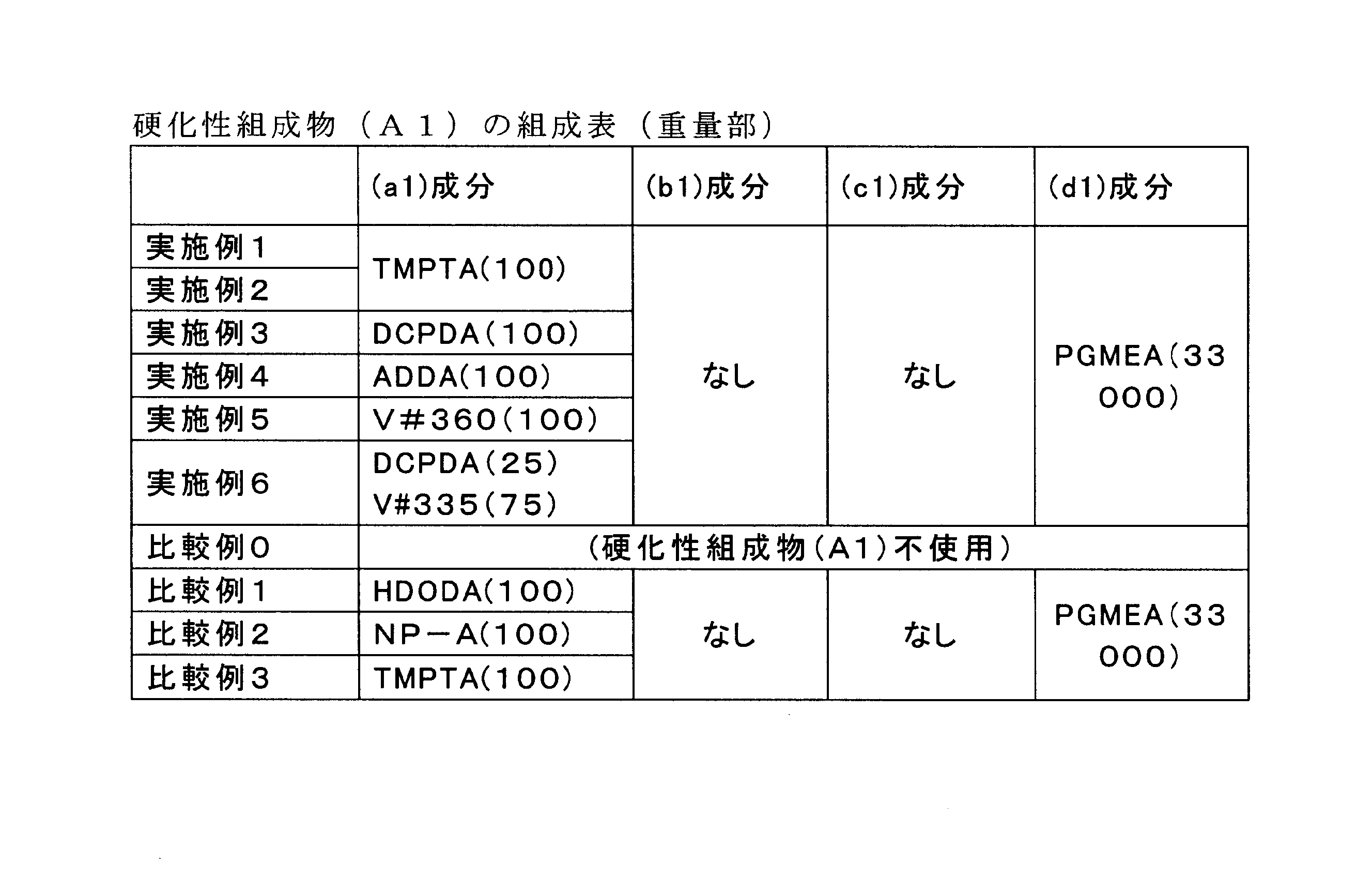


102 硬化性組成物
104 液滴の拡がる方向
105 モールド
106 照射光
107 パターン形状を有する硬化膜
108 残膜
202 硬化性組成物(A1)
203 硬化性組成物(A2)
204 液滴の拡がる方向
205 モールド
206 照射光
207 パターン形状を有する硬化膜
302 硬化性組成物(A1)
303 硬化性組成物(A2)
304 第一ショット領域
305 第二ショット領域
306 照射光
307 雰囲気制御の気体
308 モールド
309 雰囲気制御気体で膜厚または組成分布が変化した硬化性組成物(A1)
310 変化した硬化性組成物(A1)上に滴下された硬化性組成物(A2)
402 容器
403 フィルタ
404 捕集管
Claims (24)
- 少なくとも重合性化合物(a1)を含む硬化性組成物(A1)からなる層を、基板の表面に積層する第一積層工程(1)、
少なくとも重合性化合物(a2)を含む硬化性組成物(A2)からなる液滴を、前記硬化性組成物(A1)からなる層の上に離散的に滴下して積層する第二積層工程(2)、
前記硬化性組成物(A1)と前記硬化性組成物(A2)とが部分的に混合してなる混合層を、モールドと前記基板の間に挟み込む型接触工程(3)、
前記モールド側から光を照射することにより、前記混合層を硬化させる光照射工程(4)、
前記モールドを硬化後の前記混合層から引き離す離型工程(5)、
を上に述べた順に有するパターン形成方法であって、
前記硬化性組成物(A1)から溶剤を除いた組成物の25℃における粘度は40mPa・s以上500mPa・s未満であり、前記第一積層工程(1)において前記硬化性組成物(A1)の液膜が形成され、
前記硬化性組成物(A2)から溶剤を除いた組成物の25℃における粘度は1mPa・s以上40mPa・s未満であり、前記第二積層工程(2)において前記硬化性組成物)(A2)の離散的に配置された液滴が形成される、
ことを特徴とするパターン形成方法。 - 溶剤を除く前記硬化性組成物(A1)の粘度が、溶剤を除く前記硬化性組成物(A2)の粘度よりも30mPa・s以上高いことを特徴とする請求項1に記載のパターン形成方法。
- 溶剤を除く前記硬化性組成物(A1)の表面張力が、溶剤を除く前記硬化性組成物(A2)の表面張力より高いことを特徴とする請求項1から2のいずれか1項に記載のパターン形成方法。
- 前記モールドの表面の材質が石英であることを特徴とする請求項1から3のいずれか1項に記載のパターン形成方法。
- 前記型接触工程が、凝縮性ガスを含む雰囲気下で行われることを特徴とする、請求項1から4のいずれか1項に記載のパターン形成方法。
- 前記滴下工程が、前記凝縮性ガスと非凝縮性ガスとの混合ガスの雰囲気下で行われることを特徴とする請求項5に記載のパターン形成方法。
- 前記非凝縮性ガスが、ヘリウムであることを特徴とする請求項6に記載のパターン形成方法。
- 前記凝縮性ガスが、1,1,1,3,3-ペンタフルオロプロパンであることを特徴とする請求項5から7のいずれか1項に記載のパターン形成方法。
- 請求項1から8のいずれか1項に記載のパターン形成方法を含むことを特徴とする加工基板の製造方法。
- 請求項1から8のいずれか1項に記載のパターン形成方法を含むことを特徴とする光学部品の製造方法。
- 請求項1から8のいずれか一項に記載のパターン形成方法を含むことを特徴とする石英モールドレプリカの製造方法。
- 前記パターンが、前記硬化性組成物の光硬化物によるナノサイズの凹凸パターンである、請求項1から8のいずれか一項に記載のパターン形成方法。
- 少なくとも重合性化合物(a1)を含む硬化性組成物(A1)からなる層を、基板の表面に積層する第一積層工程(1)、
少なくとも重合性化合物(a2)を含む硬化性組成物(A2)の液滴を、前記硬化性組成物(A1)からなる層の上に離散的に滴下して積層する第二積層工程(2)、
前記硬化性組成物(A1)と前記硬化性組成物(A2)とが部分的に混合してなる混合層を、モールドと前記基板の間に挟み込む型接触工程(3)、
前記モールド側から光を照射することにより、前記混合層を硬化させる光照射工程(4)、及び
前記モールドを硬化後の前記混合層から引き離す離型工程(5)、
を上に述べた順に有するパターン形成方法であって、
前記硬化性組成物(A1)から溶剤を除いた組成物の25℃における粘度が20mPa・s以上500mPa・s未満であり、前記第一積層工程(1)において前記硬化性組成物(A1)の液膜が形成され、その液膜の揮発量が10μg/m3以下であり、但し、液膜の揮発量とは、液膜を300mmφの基板に塗布形成して0.8m3の容器に収め、該容器に露点-40℃以下の空気を0.3L/分で30分間通気して捕集管で捕集し、捕集した空気9L中に含まれる揮発成分の全量をガスクロマトグラフィーを用いて測定することにより求められる値であり、
前記硬化性組成物(A2)から溶剤を除いた組成物の25℃における粘度が1mPa・s以上40mPa・s未満であり、前記第二積層工程(2)において前記硬化性組成物(A1)からなる層の上に離散的に配置された前記硬化性組成物(A2)の液滴が形成される、
ことを特徴とするパターン形成方法。 - 前記硬化性組成物(A1)から溶剤を除いた組成物の粘度が、前記硬化性組成物(A2)から溶剤を除いた組成物の粘度よりも20mPa・s以上高いことを特徴とする請求項13に記載のパターン形成方法。
- 前記硬化性組成物(A1)から溶剤を除いた組成物の表面張力が、前記硬化性組成物(A2)から溶剤を除いた組成物の表面張力より高いことを特徴とする請求項13または14に記載のパターン形成方法。
- 請求項13から15のいずれか一項に記載のパターン形成方法を含むことを特徴とする加工基板の製造方法。
- 請求項13から15のいずれか一項に記載のパターン形成方法を含むことを特徴とする光学部品の製造方法。
- 請求項13から15のいずれか一項に記載のパターン形成方法を含むことを特徴とする石英モールドレプリカの製造方法。
- 基板上に前処理コーティングとなる液膜を形成し、前記液膜に対し液滴を付与することで液滴成分の基板面方向の広がりを促進するインプリント前処理コーティング材料であって、
前記インプリント前処理コーティング材料は重合性成分を有し、
溶剤を除く前記前処理コーティング材料の25℃における粘度は40mPa・s以上500mPa・s未満であり、前記付与する液滴の25℃における粘度は1mPa・s以上40mPa・s未満である、ことを特徴とするインプリント前処理コーティング材料。 - 請求項19に記載のインプリント前処理コーティング材料と、前記インプリント前処理コーティング材料でコーティングされた基板に滴下するためのインプリントレジストと、を有するセット。
- 前記インプリント前処理コーティング材料から溶媒を除いた組成物の表面張力が、前記インプリントレジストから溶媒を除いた組成物の表面張力より高いことを特徴とする請求項20に記載のセット。
- 請求項21に記載のセットに用いるインプリントレジスト。
- 基板上に硬化性組成物を配置してインプリントを行うための前処理方法であって、請求項19に記載のインプリント前処理コーティング材料を基板上にコーティングすることを特徴とする基板の前処理方法。
- 基板上にパターンを形成するためのパターン形成方法であって、請求項19に記載のインプリント前処理コーティング材料がコーティングされた基板上にレジストを不連続に滴下する工程を有することを特徴とするパターン形成方法。
Priority Applications (3)
| Application Number | Priority Date | Filing Date | Title |
|---|---|---|---|
| KR1020187030397A KR102208727B1 (ko) | 2016-03-31 | 2017-03-23 | 패턴 형성 방법, 가공 기판의 제조 방법, 광학 부품의 제조 방법, 회로 기판의 제조 방법, 전자 부품의 제조 방법, 임프린트 몰드의 제조 방법 |
| CN201780022065.8A CN109075031B (zh) | 2016-03-31 | 2017-03-23 | 图案形成方法、加工基板的制造方法、光学部件的制造方法、电路板的制造方法、电子部件的制造方法和压印模具的制造方法 |
| JP2018509179A JP6884757B2 (ja) | 2016-03-31 | 2017-03-23 | パターン形成方法、加工基板の製造方法、光学部品の製造方法、回路基板の製造方法、電子部品の製造方法、インプリントモールドの製造方法 |
Applications Claiming Priority (4)
| Application Number | Priority Date | Filing Date | Title |
|---|---|---|---|
| US201662315734P | 2016-03-31 | 2016-03-31 | |
| US62/315,734 | 2016-03-31 | ||
| US15/426,282 | 2017-02-07 | ||
| US15/426,282 US10883006B2 (en) | 2016-03-31 | 2017-02-07 | Pattern forming method as well as production methods for processed substrate, optical component, circuit board, electronic component and imprint mold |
Publications (1)
| Publication Number | Publication Date |
|---|---|
| WO2017170128A1 true WO2017170128A1 (ja) | 2017-10-05 |
Family
ID=59959190
Family Applications (1)
| Application Number | Title | Priority Date | Filing Date |
|---|---|---|---|
| PCT/JP2017/011736 Ceased WO2017170128A1 (ja) | 2016-03-31 | 2017-03-23 | パターン形成方法、加工基板の製造方法、光学部品の製造方法、回路基板の製造方法、電子部品の製造方法、インプリントモールドの製造方法 |
Country Status (6)
| Country | Link |
|---|---|
| US (1) | US10883006B2 (ja) |
| JP (1) | JP6884757B2 (ja) |
| KR (1) | KR102208727B1 (ja) |
| CN (1) | CN109075031B (ja) |
| TW (1) | TWI629160B (ja) |
| WO (1) | WO2017170128A1 (ja) |
Cited By (2)
| Publication number | Priority date | Publication date | Assignee | Title |
|---|---|---|---|---|
| WO2018051961A1 (ja) * | 2016-09-16 | 2018-03-22 | 富士フイルム株式会社 | パターン形成方法および半導体素子の製造方法 |
| WO2020059603A1 (ja) * | 2018-09-18 | 2020-03-26 | 富士フイルム株式会社 | インプリント用積層体、インプリント用積層体の製造方法、パターン形成方法およびキット |
Families Citing this family (24)
| Publication number | Priority date | Publication date | Assignee | Title |
|---|---|---|---|---|
| US10488753B2 (en) | 2015-09-08 | 2019-11-26 | Canon Kabushiki Kaisha | Substrate pretreatment and etch uniformity in nanoimprint lithography |
| US20170066208A1 (en) | 2015-09-08 | 2017-03-09 | Canon Kabushiki Kaisha | Substrate pretreatment for reducing fill time in nanoimprint lithography |
| US10134588B2 (en) | 2016-03-31 | 2018-11-20 | Canon Kabushiki Kaisha | Imprint resist and substrate pretreatment for reducing fill time in nanoimprint lithography |
| US10095106B2 (en) | 2016-03-31 | 2018-10-09 | Canon Kabushiki Kaisha | Removing substrate pretreatment compositions in nanoimprint lithography |
| US10754244B2 (en) | 2016-03-31 | 2020-08-25 | Canon Kabushiki Kaisha | Pattern forming method as well as production methods for processed substrate, optical component, circuit board, electronic component and imprint mold |
| US10620539B2 (en) | 2016-03-31 | 2020-04-14 | Canon Kabushiki Kaisha | Curing substrate pretreatment compositions in nanoimprint lithography |
| US10578965B2 (en) | 2016-03-31 | 2020-03-03 | Canon Kabushiki Kaisha | Pattern forming method |
| US10845700B2 (en) | 2016-03-31 | 2020-11-24 | Canon Kabushiki Kaisha | Pattern forming method as well as production methods for processed substrate, optical component, circuit board, electronic component and imprint mold |
| US10754243B2 (en) | 2016-03-31 | 2020-08-25 | Canon Kabushiki Kaisha | Pattern forming method as well as production methods for processed substrate, optical component, circuit board, electronic component and imprint mold |
| US10754245B2 (en) | 2016-03-31 | 2020-08-25 | Canon Kabushiki Kaisha | Pattern forming method as well as production methods for processed substrate, optical component, circuit board, electronic component and imprint mold |
| US10829644B2 (en) | 2016-03-31 | 2020-11-10 | Canon Kabushiki Kaisha | Pattern forming method as well as production methods for processed substrate, optical component, circuit board, electronic component and imprint mold |
| WO2017175668A1 (ja) * | 2016-04-08 | 2017-10-12 | キヤノン株式会社 | 硬化物パターンの形成方法、加工基板の製造方法、光学部品の製造方法、回路基板の製造方法、電子部品の製造方法、インプリントモールドの製造方法、およびインプリント前処理コート用材料 |
| US10509313B2 (en) | 2016-06-28 | 2019-12-17 | Canon Kabushiki Kaisha | Imprint resist with fluorinated photoinitiator and substrate pretreatment for reducing fill time in nanoimprint lithography |
| US10317793B2 (en) | 2017-03-03 | 2019-06-11 | Canon Kabushiki Kaisha | Substrate pretreatment compositions for nanoimprint lithography |
| JP7328888B2 (ja) | 2017-03-08 | 2023-08-17 | キヤノン株式会社 | 硬化物パターンの製造方法、光学部品、回路基板および石英モールドレプリカの製造方法、ならびにインプリント前処理コート用材料およびその硬化物 |
| JP7071331B2 (ja) | 2017-03-08 | 2022-05-18 | キヤノン株式会社 | 光ナノインプリント技術を用いたパターン形成方法、インプリント装置、および硬化性組成物 |
| KR102385158B1 (ko) | 2017-03-08 | 2022-04-12 | 캐논 가부시끼가이샤 | 패턴 형성 방법, 임프린트 전처리 코팅 재료, 및 기판의 전처리 방법 |
| KR102256347B1 (ko) | 2017-03-08 | 2021-05-27 | 캐논 가부시끼가이샤 | 패턴 형성 방법, 및 가공 기판, 광학 부품 및 석영 몰드 레플리카의 제조 방법, 및 임프린트 전처리 코팅 재료 및 그와 임프린트 레지스트와의 세트 |
| KR102419881B1 (ko) | 2017-08-10 | 2022-07-12 | 캐논 가부시끼가이샤 | 패턴 형성 방법 |
| JP7060451B2 (ja) * | 2018-06-06 | 2022-04-26 | 東芝ライフスタイル株式会社 | 酸素富化膜の製造方法 |
| CN111319175B (zh) * | 2019-01-15 | 2022-06-07 | 陈龙 | 耳机壳及其制作方法 |
| US12360455B2 (en) * | 2019-02-08 | 2025-07-15 | Brewer Science, Inc. | Poly(cyanocinnamate)s for structural and optical applications |
| US11249397B2 (en) * | 2019-11-22 | 2022-02-15 | Canon Kabushiki Kaisha | Method of forming a cured layer by controlling drop spreading |
| US11752519B2 (en) | 2020-06-19 | 2023-09-12 | Canon Kabushiki Kaisha | Planarization method and photocurable composition |
Citations (7)
| Publication number | Priority date | Publication date | Assignee | Title |
|---|---|---|---|---|
| JP2010508662A (ja) * | 2006-10-27 | 2010-03-18 | ザ ボード オブ トラスティーズ オブ ザ ユニヴァーシティー オブ イリノイ | インクリソグラフィによるパターン生成デバイスおよび方法 |
| JP2011508680A (ja) * | 2007-12-04 | 2011-03-17 | モレキュラー・インプリンツ・インコーポレーテッド | 極薄ポリマー接着層 |
| WO2011155602A1 (ja) * | 2010-06-11 | 2011-12-15 | Hoya株式会社 | 密着補助層付き基板、モールドの製造方法及びマスターモールドの製造方法 |
| JP2014093385A (ja) * | 2012-11-02 | 2014-05-19 | Fujifilm Corp | インプリント用密着膜の製造方法およびパターン形成方法 |
| JP2015130535A (ja) * | 2015-04-02 | 2015-07-16 | 大日本印刷株式会社 | インプリント用基板およびインプリント方法 |
| JP2016028419A (ja) * | 2014-07-08 | 2016-02-25 | キヤノン株式会社 | 密着層組成物、ナノインプリントによる膜の製造方法、光学部品の製造方法、回路基板の製造方法、および電子機器の製造方法 |
| JP2017055108A (ja) * | 2015-09-08 | 2017-03-16 | キヤノン株式会社 | ナノインプリントリソグラフィーにおける充填時間を短縮するための基板の前処理 |
Family Cites Families (44)
| Publication number | Priority date | Publication date | Assignee | Title |
|---|---|---|---|---|
| WO2004086471A1 (en) * | 2003-03-27 | 2004-10-07 | Korea Institute Of Machinery & Materials | Uv nanoimprint lithography process using elementwise embossed stamp and selectively additive pressurization |
| US20050160934A1 (en) | 2004-01-23 | 2005-07-28 | Molecular Imprints, Inc. | Materials and methods for imprint lithography |
| US7307118B2 (en) | 2004-11-24 | 2007-12-11 | Molecular Imprints, Inc. | Composition to reduce adhesion between a conformable region and a mold |
| US7157036B2 (en) | 2003-06-17 | 2007-01-02 | Molecular Imprints, Inc | Method to reduce adhesion between a conformable region and a pattern of a mold |
| US20060108710A1 (en) | 2004-11-24 | 2006-05-25 | Molecular Imprints, Inc. | Method to reduce adhesion between a conformable region and a mold |
| US7195733B2 (en) | 2004-04-27 | 2007-03-27 | The Board Of Trustees Of The University Of Illinois | Composite patterning devices for soft lithography |
| US8808808B2 (en) | 2005-07-22 | 2014-08-19 | Molecular Imprints, Inc. | Method for imprint lithography utilizing an adhesion primer layer |
| US7759407B2 (en) | 2005-07-22 | 2010-07-20 | Molecular Imprints, Inc. | Composition for adhering materials together |
| US8557351B2 (en) | 2005-07-22 | 2013-10-15 | Molecular Imprints, Inc. | Method for adhering materials together |
| US8142703B2 (en) | 2005-10-05 | 2012-03-27 | Molecular Imprints, Inc. | Imprint lithography method |
| JP5274128B2 (ja) * | 2007-08-03 | 2013-08-28 | キヤノン株式会社 | インプリント方法および基板の加工方法 |
| JP5065101B2 (ja) | 2008-03-05 | 2012-10-31 | 東洋合成工業株式会社 | パターン形成方法 |
| JP2010106185A (ja) | 2008-10-31 | 2010-05-13 | Fujifilm Corp | 光インプリント用硬化性組成物およびそれを用いたパターン形成方法 |
| WO2011027845A1 (en) | 2009-09-02 | 2011-03-10 | Canon Kabushiki Kaisha | Manufacturing method for plastic member and plastic member |
| JP5483083B2 (ja) | 2010-02-03 | 2014-05-07 | 富士フイルム株式会社 | 微細パターン製造方法 |
| JP5596367B2 (ja) | 2010-02-22 | 2014-09-24 | 富士フイルム株式会社 | パターン製造方法 |
| JP5463170B2 (ja) | 2010-03-10 | 2014-04-09 | 富士フイルム株式会社 | 微細パターン製造方法、微細パターン付き基板、微細パターン付き基板を含む光源装置および画像表示装置 |
| JP5599648B2 (ja) | 2010-05-12 | 2014-10-01 | 富士フイルム株式会社 | 微細パターン製造方法および微細パターン付き基板 |
| JP5533297B2 (ja) * | 2010-06-09 | 2014-06-25 | 大日本印刷株式会社 | インプリント方法 |
| JP6012344B2 (ja) | 2011-10-24 | 2016-10-25 | キヤノン株式会社 | 膜の形成方法 |
| JP5959865B2 (ja) | 2012-02-09 | 2016-08-02 | キヤノン株式会社 | 光硬化物及びその製造方法 |
| JP2013222791A (ja) * | 2012-04-16 | 2013-10-28 | Fujifilm Corp | ナノインプリント方法およびナノインプリント用基板並びにそれらを用いたパターン化基板の製造方法 |
| JP5930832B2 (ja) | 2012-04-27 | 2016-06-08 | キヤノン株式会社 | 光硬化物の製造方法 |
| JP6071255B2 (ja) | 2012-06-04 | 2017-02-01 | キヤノン株式会社 | 光硬化物 |
| JP5827180B2 (ja) | 2012-06-18 | 2015-12-02 | 富士フイルム株式会社 | インプリント用硬化性組成物と基板の密着用組成物およびこれを用いた半導体デバイス |
| JP6000712B2 (ja) | 2012-07-24 | 2016-10-05 | キヤノン株式会社 | 樹脂の製造方法及び樹脂の製造装置 |
| JP6278645B2 (ja) | 2012-09-24 | 2018-02-14 | キヤノン株式会社 | 光硬化性組成物及びこれを用いた膜の製造方法 |
| JP6748399B2 (ja) | 2012-11-30 | 2020-09-02 | キヤノン株式会社 | インプリント方法およびインプリント用硬化性組成物 |
| JP6305058B2 (ja) | 2013-03-05 | 2018-04-04 | キヤノン株式会社 | 感光性ガス発生剤、光硬化性組成物 |
| JP6047049B2 (ja) | 2013-03-27 | 2016-12-21 | 富士フイルム株式会社 | 組成物、硬化物、積層体、下層膜の製造方法、パターン形成方法、パターンおよび半導体レジストの製造方法 |
| JP6167057B2 (ja) * | 2013-05-31 | 2017-07-19 | Jxtgエネルギー株式会社 | 凹凸パターン転写用モールドの製造方法及び凹凸構造を有する部材の製造方法 |
| JP6327948B2 (ja) | 2013-06-26 | 2018-05-23 | キヤノン株式会社 | 光硬化性組成物、硬化物、これを用いた、膜の製造方法、光学部品の製造方法、回路基板の製造方法、電子部品の製造方法 |
| JP6328001B2 (ja) | 2013-08-30 | 2018-05-23 | キヤノン株式会社 | インプリント用硬化性組成物、膜、膜の製造方法 |
| JP6460672B2 (ja) | 2013-09-18 | 2019-01-30 | キヤノン株式会社 | 膜の製造方法、光学部品の製造方法、回路基板の製造方法及び電子部品の製造方法 |
| CN104330841B (zh) * | 2014-10-30 | 2016-05-04 | 西安交通大学 | 一种数值孔径可控的微透镜阵列的电辅助制造方法 |
| US20170068159A1 (en) * | 2015-09-08 | 2017-03-09 | Canon Kabushiki Kaisha | Substrate pretreatment for reducing fill time in nanoimprint lithography |
| JP6961495B2 (ja) | 2016-01-25 | 2021-11-05 | キヤノン株式会社 | パターン形成方法、加工基板の製造方法、光学部品の製造方法、回路基板の製造方法、電子部品の製造方法、インプリントモールドの製造方法 |
| US10578965B2 (en) | 2016-03-31 | 2020-03-03 | Canon Kabushiki Kaisha | Pattern forming method |
| US10754245B2 (en) * | 2016-03-31 | 2020-08-25 | Canon Kabushiki Kaisha | Pattern forming method as well as production methods for processed substrate, optical component, circuit board, electronic component and imprint mold |
| US10829644B2 (en) | 2016-03-31 | 2020-11-10 | Canon Kabushiki Kaisha | Pattern forming method as well as production methods for processed substrate, optical component, circuit board, electronic component and imprint mold |
| US10845700B2 (en) | 2016-03-31 | 2020-11-24 | Canon Kabushiki Kaisha | Pattern forming method as well as production methods for processed substrate, optical component, circuit board, electronic component and imprint mold |
| US10754244B2 (en) | 2016-03-31 | 2020-08-25 | Canon Kabushiki Kaisha | Pattern forming method as well as production methods for processed substrate, optical component, circuit board, electronic component and imprint mold |
| US10754243B2 (en) * | 2016-03-31 | 2020-08-25 | Canon Kabushiki Kaisha | Pattern forming method as well as production methods for processed substrate, optical component, circuit board, electronic component and imprint mold |
| WO2017175668A1 (ja) | 2016-04-08 | 2017-10-12 | キヤノン株式会社 | 硬化物パターンの形成方法、加工基板の製造方法、光学部品の製造方法、回路基板の製造方法、電子部品の製造方法、インプリントモールドの製造方法、およびインプリント前処理コート用材料 |
-
2017
- 2017-02-07 US US15/426,282 patent/US10883006B2/en active Active
- 2017-03-23 JP JP2018509179A patent/JP6884757B2/ja active Active
- 2017-03-23 CN CN201780022065.8A patent/CN109075031B/zh active Active
- 2017-03-23 KR KR1020187030397A patent/KR102208727B1/ko active Active
- 2017-03-23 WO PCT/JP2017/011736 patent/WO2017170128A1/ja not_active Ceased
- 2017-03-30 TW TW106110850A patent/TWI629160B/zh active
Patent Citations (7)
| Publication number | Priority date | Publication date | Assignee | Title |
|---|---|---|---|---|
| JP2010508662A (ja) * | 2006-10-27 | 2010-03-18 | ザ ボード オブ トラスティーズ オブ ザ ユニヴァーシティー オブ イリノイ | インクリソグラフィによるパターン生成デバイスおよび方法 |
| JP2011508680A (ja) * | 2007-12-04 | 2011-03-17 | モレキュラー・インプリンツ・インコーポレーテッド | 極薄ポリマー接着層 |
| WO2011155602A1 (ja) * | 2010-06-11 | 2011-12-15 | Hoya株式会社 | 密着補助層付き基板、モールドの製造方法及びマスターモールドの製造方法 |
| JP2014093385A (ja) * | 2012-11-02 | 2014-05-19 | Fujifilm Corp | インプリント用密着膜の製造方法およびパターン形成方法 |
| JP2016028419A (ja) * | 2014-07-08 | 2016-02-25 | キヤノン株式会社 | 密着層組成物、ナノインプリントによる膜の製造方法、光学部品の製造方法、回路基板の製造方法、および電子機器の製造方法 |
| JP2015130535A (ja) * | 2015-04-02 | 2015-07-16 | 大日本印刷株式会社 | インプリント用基板およびインプリント方法 |
| JP2017055108A (ja) * | 2015-09-08 | 2017-03-16 | キヤノン株式会社 | ナノインプリントリソグラフィーにおける充填時間を短縮するための基板の前処理 |
Cited By (3)
| Publication number | Priority date | Publication date | Assignee | Title |
|---|---|---|---|---|
| WO2018051961A1 (ja) * | 2016-09-16 | 2018-03-22 | 富士フイルム株式会社 | パターン形成方法および半導体素子の製造方法 |
| JPWO2018051961A1 (ja) * | 2016-09-16 | 2019-08-08 | 富士フイルム株式会社 | パターン形成方法および半導体素子の製造方法 |
| WO2020059603A1 (ja) * | 2018-09-18 | 2020-03-26 | 富士フイルム株式会社 | インプリント用積層体、インプリント用積層体の製造方法、パターン形成方法およびキット |
Also Published As
| Publication number | Publication date |
|---|---|
| US20170283632A1 (en) | 2017-10-05 |
| CN109075031A (zh) | 2018-12-21 |
| CN109075031B (zh) | 2023-05-16 |
| TWI629160B (zh) | 2018-07-11 |
| KR102208727B1 (ko) | 2021-01-28 |
| TW201736085A (zh) | 2017-10-16 |
| JPWO2017170128A1 (ja) | 2019-02-14 |
| KR20180126026A (ko) | 2018-11-26 |
| JP6884757B2 (ja) | 2021-06-09 |
| US10883006B2 (en) | 2021-01-05 |
Similar Documents
| Publication | Publication Date | Title |
|---|---|---|
| JP6884757B2 (ja) | パターン形成方法、加工基板の製造方法、光学部品の製造方法、回路基板の製造方法、電子部品の製造方法、インプリントモールドの製造方法 | |
| JP6806766B2 (ja) | パターン形成方法、加工基板の製造方法、光学部品の製造方法、回路基板の製造方法、電子部品の製造方法、インプリントモールドの製造方法 | |
| JP6983757B2 (ja) | パターン形成方法、加工基板の製造方法、光学部品の製造方法、回路基板の製造方法、電子部品の製造方法、インプリントモールドの製造方法 | |
| JP7155002B2 (ja) | パターン形成方法、加工基板の製造方法、光学部品の製造方法、回路基板の製造方法、電子部品の製造方法、インプリントモールドの製造方法 | |
| JP7328888B2 (ja) | 硬化物パターンの製造方法、光学部品、回路基板および石英モールドレプリカの製造方法、ならびにインプリント前処理コート用材料およびその硬化物 | |
| JP7086841B2 (ja) | パターン形成方法、加工基板の製造方法、光学部品の製造方法、回路基板の製造方法、電子部品の製造方法、インプリントモールドの製造方法 | |
| JP7066674B2 (ja) | パターン形成方法、インプリント前処理コーティング材料、及び基板の前処理方法 | |
| JP7094878B2 (ja) | パターン形成方法、加工基板の製造方法、光学部品の製造方法、石英モールドレプリカの製造方法、半導体素子の製造方法 | |
| JP7425602B2 (ja) | パターン形成方法、ならびに加工基板、光学部品及び石英モールドレプリカの製造方法、ならびにインプリント前処理コーティング材料及びそれとインプリントレジストとのセット | |
| JPWO2017170697A1 (ja) | パターン形成方法、加工基板の製造方法、光学部品の製造方法、回路基板の製造方法、電子部品の製造方法、インプリントモールドの製造方法 | |
| WO2017130853A1 (ja) | パターン形成方法、加工基板の製造方法、光学部品の製造方法、回路基板の製造方法、電子部品の製造方法、インプリントモールドの製造方法 | |
| JP6324363B2 (ja) | インプリント用光硬化性組成物、これを用いた膜の製造方法、光学部品の製造方法、回路基板の製造方法、電子部品の製造方法 | |
| WO2017175668A1 (ja) | 硬化物パターンの形成方法、加工基板の製造方法、光学部品の製造方法、回路基板の製造方法、電子部品の製造方法、インプリントモールドの製造方法、およびインプリント前処理コート用材料 | |
| JP2015179807A (ja) | 光インプリント用組成物、これを用いた、膜の製造方法、光学部品の製造方法、回路基板の製造方法、電子部品の製造方法 | |
| WO2018164016A1 (ja) | 光ナノインプリント技術を用いたパターン形成方法、インプリント装置、および硬化性組成物 | |
| JP2016162862A (ja) | パターンの形成方法、加工基板の製造方法、光学部品の製造方法、回路基板の製造方法、電子部品の製造方法 | |
| JP2016029138A (ja) | 硬化性組成物、その硬化物、硬化物の製造方法、光学部品の製造方法、回路基板の製造方法、および電子部品の製造方法 | |
| JP2016030829A (ja) | 光硬化性組成物、これを用いた硬化物パターンの製造方法、光学部品の製造方法、回路基板の製造方法 | |
| JP2016047913A (ja) | 光硬化性組成物、これを用いた硬化物パターンの製造方法、光学部品の製造方法、回路基板の製造方法、およびインプリント用モールドの製造方法 | |
| JP2017085148A (ja) | 光インプリント用組成物、これを用いた、膜の製造方法、光学部品の製造方法、回路基板の製造方法、電子部品の製造方法 |
Legal Events
| Date | Code | Title | Description |
|---|---|---|---|
| WWE | Wipo information: entry into national phase |
Ref document number: 2018509179 Country of ref document: JP |
|
| NENP | Non-entry into the national phase |
Ref country code: DE |
|
| ENP | Entry into the national phase |
Ref document number: 20187030397 Country of ref document: KR Kind code of ref document: A |
|
| 121 | Ep: the epo has been informed by wipo that ep was designated in this application |
Ref document number: 17774666 Country of ref document: EP Kind code of ref document: A1 |
|
| 122 | Ep: pct application non-entry in european phase |
Ref document number: 17774666 Country of ref document: EP Kind code of ref document: A1 |