WO2015115237A1 - 透明電極付き基板およびその製造方法 - Google Patents
透明電極付き基板およびその製造方法 Download PDFInfo
- Publication number
- WO2015115237A1 WO2015115237A1 PCT/JP2015/051286 JP2015051286W WO2015115237A1 WO 2015115237 A1 WO2015115237 A1 WO 2015115237A1 JP 2015051286 W JP2015051286 W JP 2015051286W WO 2015115237 A1 WO2015115237 A1 WO 2015115237A1
- Authority
- WO
- WIPO (PCT)
- Prior art keywords
- transparent electrode
- thin film
- substrate
- electrode thin
- film
- Prior art date
- Legal status (The legal status is an assumption and is not a legal conclusion. Google has not performed a legal analysis and makes no representation as to the accuracy of the status listed.)
- Ceased
Links
Images




Classifications
-
- C—CHEMISTRY; METALLURGY
- C23—COATING METALLIC MATERIAL; COATING MATERIAL WITH METALLIC MATERIAL; CHEMICAL SURFACE TREATMENT; DIFFUSION TREATMENT OF METALLIC MATERIAL; COATING BY VACUUM EVAPORATION, BY SPUTTERING, BY ION IMPLANTATION OR BY CHEMICAL VAPOUR DEPOSITION, IN GENERAL; INHIBITING CORROSION OF METALLIC MATERIAL OR INCRUSTATION IN GENERAL
- C23C—COATING METALLIC MATERIAL; COATING MATERIAL WITH METALLIC MATERIAL; SURFACE TREATMENT OF METALLIC MATERIAL BY DIFFUSION INTO THE SURFACE, BY CHEMICAL CONVERSION OR SUBSTITUTION; COATING BY VACUUM EVAPORATION, BY SPUTTERING, BY ION IMPLANTATION OR BY CHEMICAL VAPOUR DEPOSITION, IN GENERAL
- C23C14/00—Coating by vacuum evaporation, by sputtering or by ion implantation of the coating forming material
- C23C14/02—Pretreatment of the material to be coated
- C23C14/024—Deposition of sublayers, e.g. to promote adhesion of the coating
-
- C—CHEMISTRY; METALLURGY
- C23—COATING METALLIC MATERIAL; COATING MATERIAL WITH METALLIC MATERIAL; CHEMICAL SURFACE TREATMENT; DIFFUSION TREATMENT OF METALLIC MATERIAL; COATING BY VACUUM EVAPORATION, BY SPUTTERING, BY ION IMPLANTATION OR BY CHEMICAL VAPOUR DEPOSITION, IN GENERAL; INHIBITING CORROSION OF METALLIC MATERIAL OR INCRUSTATION IN GENERAL
- C23C—COATING METALLIC MATERIAL; COATING MATERIAL WITH METALLIC MATERIAL; SURFACE TREATMENT OF METALLIC MATERIAL BY DIFFUSION INTO THE SURFACE, BY CHEMICAL CONVERSION OR SUBSTITUTION; COATING BY VACUUM EVAPORATION, BY SPUTTERING, BY ION IMPLANTATION OR BY CHEMICAL VAPOUR DEPOSITION, IN GENERAL
- C23C14/00—Coating by vacuum evaporation, by sputtering or by ion implantation of the coating forming material
- C23C14/06—Coating by vacuum evaporation, by sputtering or by ion implantation of the coating forming material characterised by the coating material
- C23C14/08—Oxides
- C23C14/083—Oxides of refractory metals or yttrium
-
- C—CHEMISTRY; METALLURGY
- C23—COATING METALLIC MATERIAL; COATING MATERIAL WITH METALLIC MATERIAL; CHEMICAL SURFACE TREATMENT; DIFFUSION TREATMENT OF METALLIC MATERIAL; COATING BY VACUUM EVAPORATION, BY SPUTTERING, BY ION IMPLANTATION OR BY CHEMICAL VAPOUR DEPOSITION, IN GENERAL; INHIBITING CORROSION OF METALLIC MATERIAL OR INCRUSTATION IN GENERAL
- C23C—COATING METALLIC MATERIAL; COATING MATERIAL WITH METALLIC MATERIAL; SURFACE TREATMENT OF METALLIC MATERIAL BY DIFFUSION INTO THE SURFACE, BY CHEMICAL CONVERSION OR SUBSTITUTION; COATING BY VACUUM EVAPORATION, BY SPUTTERING, BY ION IMPLANTATION OR BY CHEMICAL VAPOUR DEPOSITION, IN GENERAL
- C23C14/00—Coating by vacuum evaporation, by sputtering or by ion implantation of the coating forming material
- C23C14/06—Coating by vacuum evaporation, by sputtering or by ion implantation of the coating forming material characterised by the coating material
- C23C14/08—Oxides
- C23C14/086—Oxides of zinc, germanium, cadmium, indium, tin, thallium or bismuth
-
- C—CHEMISTRY; METALLURGY
- C23—COATING METALLIC MATERIAL; COATING MATERIAL WITH METALLIC MATERIAL; CHEMICAL SURFACE TREATMENT; DIFFUSION TREATMENT OF METALLIC MATERIAL; COATING BY VACUUM EVAPORATION, BY SPUTTERING, BY ION IMPLANTATION OR BY CHEMICAL VAPOUR DEPOSITION, IN GENERAL; INHIBITING CORROSION OF METALLIC MATERIAL OR INCRUSTATION IN GENERAL
- C23C—COATING METALLIC MATERIAL; COATING MATERIAL WITH METALLIC MATERIAL; SURFACE TREATMENT OF METALLIC MATERIAL BY DIFFUSION INTO THE SURFACE, BY CHEMICAL CONVERSION OR SUBSTITUTION; COATING BY VACUUM EVAPORATION, BY SPUTTERING, BY ION IMPLANTATION OR BY CHEMICAL VAPOUR DEPOSITION, IN GENERAL
- C23C14/00—Coating by vacuum evaporation, by sputtering or by ion implantation of the coating forming material
- C23C14/22—Coating by vacuum evaporation, by sputtering or by ion implantation of the coating forming material characterised by the process of coating
- C23C14/34—Sputtering
- C23C14/35—Sputtering by application of a magnetic field, e.g. magnetron sputtering
-
- C—CHEMISTRY; METALLURGY
- C23—COATING METALLIC MATERIAL; COATING MATERIAL WITH METALLIC MATERIAL; CHEMICAL SURFACE TREATMENT; DIFFUSION TREATMENT OF METALLIC MATERIAL; COATING BY VACUUM EVAPORATION, BY SPUTTERING, BY ION IMPLANTATION OR BY CHEMICAL VAPOUR DEPOSITION, IN GENERAL; INHIBITING CORROSION OF METALLIC MATERIAL OR INCRUSTATION IN GENERAL
- C23C—COATING METALLIC MATERIAL; COATING MATERIAL WITH METALLIC MATERIAL; SURFACE TREATMENT OF METALLIC MATERIAL BY DIFFUSION INTO THE SURFACE, BY CHEMICAL CONVERSION OR SUBSTITUTION; COATING BY VACUUM EVAPORATION, BY SPUTTERING, BY ION IMPLANTATION OR BY CHEMICAL VAPOUR DEPOSITION, IN GENERAL
- C23C14/00—Coating by vacuum evaporation, by sputtering or by ion implantation of the coating forming material
- C23C14/58—After-treatment
- C23C14/5806—Thermal treatment
-
- G—PHYSICS
- G06—COMPUTING OR CALCULATING; COUNTING
- G06F—ELECTRIC DIGITAL DATA PROCESSING
- G06F3/00—Input arrangements for transferring data to be processed into a form capable of being handled by the computer; Output arrangements for transferring data from processing unit to output unit, e.g. interface arrangements
- G06F3/01—Input arrangements or combined input and output arrangements for interaction between user and computer
- G06F3/03—Arrangements for converting the position or the displacement of a member into a coded form
- G06F3/041—Digitisers, e.g. for touch screens or touch pads, characterised by the transducing means
-
- H—ELECTRICITY
- H10—SEMICONDUCTOR DEVICES; ELECTRIC SOLID-STATE DEVICES NOT OTHERWISE PROVIDED FOR
- H10F—INORGANIC SEMICONDUCTOR DEVICES SENSITIVE TO INFRARED RADIATION, LIGHT, ELECTROMAGNETIC RADIATION OF SHORTER WAVELENGTH OR CORPUSCULAR RADIATION
- H10F77/00—Constructional details of devices covered by this subclass
- H10F77/10—Semiconductor bodies
- H10F77/16—Material structures, e.g. crystalline structures, film structures or crystal plane orientations
- H10F77/169—Thin semiconductor films on metallic or insulating substrates
-
- H—ELECTRICITY
- H10—SEMICONDUCTOR DEVICES; ELECTRIC SOLID-STATE DEVICES NOT OTHERWISE PROVIDED FOR
- H10F—INORGANIC SEMICONDUCTOR DEVICES SENSITIVE TO INFRARED RADIATION, LIGHT, ELECTROMAGNETIC RADIATION OF SHORTER WAVELENGTH OR CORPUSCULAR RADIATION
- H10F77/00—Constructional details of devices covered by this subclass
- H10F77/20—Electrodes
- H10F77/206—Electrodes for devices having potential barriers
- H10F77/211—Electrodes for devices having potential barriers for photovoltaic cells
-
- H—ELECTRICITY
- H10—SEMICONDUCTOR DEVICES; ELECTRIC SOLID-STATE DEVICES NOT OTHERWISE PROVIDED FOR
- H10F—INORGANIC SEMICONDUCTOR DEVICES SENSITIVE TO INFRARED RADIATION, LIGHT, ELECTROMAGNETIC RADIATION OF SHORTER WAVELENGTH OR CORPUSCULAR RADIATION
- H10F77/00—Constructional details of devices covered by this subclass
- H10F77/20—Electrodes
- H10F77/244—Electrodes made of transparent conductive layers, e.g. transparent conductive oxide [TCO] layers
-
- H—ELECTRICITY
- H10—SEMICONDUCTOR DEVICES; ELECTRIC SOLID-STATE DEVICES NOT OTHERWISE PROVIDED FOR
- H10F—INORGANIC SEMICONDUCTOR DEVICES SENSITIVE TO INFRARED RADIATION, LIGHT, ELECTROMAGNETIC RADIATION OF SHORTER WAVELENGTH OR CORPUSCULAR RADIATION
- H10F77/00—Constructional details of devices covered by this subclass
- H10F77/20—Electrodes
- H10F77/244—Electrodes made of transparent conductive layers, e.g. transparent conductive oxide [TCO] layers
- H10F77/251—Electrodes made of transparent conductive layers, e.g. transparent conductive oxide [TCO] layers comprising zinc oxide [ZnO]
-
- H—ELECTRICITY
- H10—SEMICONDUCTOR DEVICES; ELECTRIC SOLID-STATE DEVICES NOT OTHERWISE PROVIDED FOR
- H10H—INORGANIC LIGHT-EMITTING SEMICONDUCTOR DEVICES HAVING POTENTIAL BARRIERS
- H10H20/00—Individual inorganic light-emitting semiconductor devices having potential barriers, e.g. light-emitting diodes [LED]
- H10H20/80—Constructional details
- H10H20/83—Electrodes
- H10H20/832—Electrodes characterised by their material
- H10H20/833—Transparent materials
-
- G—PHYSICS
- G06—COMPUTING OR CALCULATING; COUNTING
- G06F—ELECTRIC DIGITAL DATA PROCESSING
- G06F2203/00—Indexing scheme relating to G06F3/00 - G06F3/048
- G06F2203/041—Indexing scheme relating to G06F3/041 - G06F3/045
- G06F2203/04103—Manufacturing, i.e. details related to manufacturing processes specially suited for touch sensitive devices
-
- G—PHYSICS
- G06—COMPUTING OR CALCULATING; COUNTING
- G06F—ELECTRIC DIGITAL DATA PROCESSING
- G06F3/00—Input arrangements for transferring data to be processed into a form capable of being handled by the computer; Output arrangements for transferring data from processing unit to output unit, e.g. interface arrangements
- G06F3/01—Input arrangements or combined input and output arrangements for interaction between user and computer
- G06F3/03—Arrangements for converting the position or the displacement of a member into a coded form
- G06F3/041—Digitisers, e.g. for touch screens or touch pads, characterised by the transducing means
- G06F3/044—Digitisers, e.g. for touch screens or touch pads, characterised by the transducing means by capacitive means
-
- Y—GENERAL TAGGING OF NEW TECHNOLOGICAL DEVELOPMENTS; GENERAL TAGGING OF CROSS-SECTIONAL TECHNOLOGIES SPANNING OVER SEVERAL SECTIONS OF THE IPC; TECHNICAL SUBJECTS COVERED BY FORMER USPC CROSS-REFERENCE ART COLLECTIONS [XRACs] AND DIGESTS
- Y02—TECHNOLOGIES OR APPLICATIONS FOR MITIGATION OR ADAPTATION AGAINST CLIMATE CHANGE
- Y02E—REDUCTION OF GREENHOUSE GAS [GHG] EMISSIONS, RELATED TO ENERGY GENERATION, TRANSMISSION OR DISTRIBUTION
- Y02E10/00—Energy generation through renewable energy sources
- Y02E10/50—Photovoltaic [PV] energy
Definitions
- the present invention relates to a substrate with a transparent electrode in which a transparent electrode thin film is formed on a film substrate and a method for manufacturing the same.
- a transparent electrode used for a display device such as a touch panel or a display
- a light-emitting device such as an LED
- a light-receiving device such as a solar cell
- the technology of heat-treating the transparent electrode thin film to lower the resistance of the transparent electrode thin film by promoting crystallization is important, and many conventional research and development have pursued the promotion of crystallization and achieved lower resistance. It was.
- Patent Document 1 describes a technique for reducing the resistance of a transparent electrode thin film by forming cerium oxide as an underlayer.
- Patent Document 2 describes a technique for promoting crystallization by forming a transparent electrode thin film into a multilayer structure.
- Patent Document 3 describes a technique in which a dielectric layer and a conductive layer are stacked on a substrate to withstand electrical characteristics and physical wear.
- Patent Document 4 discloses a method for producing a transparent conductive film which does not require heating at a high temperature and can be crystallized by heating at room temperature or low temperature.
- Patent Document 4 describes that electrical characteristics may change when a substrate with a transparent electrode is stored for a long time in a room temperature environment. This is a phenomenon in which an amorphous transparent electrode thin film is transformed into a thermodynamically stable crystalline material in a room temperature environment and electrical characteristics are changed.
- crystallization occurs in such a normal temperature environment, internal stress is generated in the transparent electrode thin film, which may cause peeling or deformation from the substrate in the subsequent device manufacturing process.
- the substrate is a soft material such as a film or plastic, the above problem is likely to occur.
- the present invention provides a substrate with a transparent electrode that can simultaneously achieve crystallization promotion during heat treatment and suppression of crystallization in a room temperature environment.
- the present invention relates to a substrate with a transparent electrode in which a transparent electrode thin film is formed on a film substrate.
- the underlayer and the transparent electrode thin film are in contact with each other.
- the transparent electrode thin film is amorphous, and the underlayer is dielectric and crystalline.
- An underlayer containing a metal oxide such as indium oxide, zinc oxide or yttrium oxide as a main component is preferably formed between the film substrate and the transparent electrode thin film.
- the film thickness of the underlayer is 2 to 15 nm from the viewpoint of suppressing the diffusion of components that inhibit crystallization of the transparent electrode thin film from the substrate and controlling the surface free energy when forming the transparent electrode thin film. It is preferable that
- the transparent electrode thin film preferably contains indium oxide as a main component. From the viewpoint of low resistance and high transparency, the thickness of the transparent electrode thin film is preferably 15 to 30 nm.
- the transparent electrode thin film has low resistance particles, and the diameter of the low resistance particles determined by current image measurement using an atomic force microscope is preferably within the film of the transparent electrode thin film. Indicates the maximum value in the central part.
- the present invention relates to a method for producing the substrate with a transparent electrode.
- the underlayer and the transparent electrode thin film are both formed by magnetron sputtering using oxygen gas, and the amount of oxygen introduced into the chamber when forming the underlayer is determined by the formation of the transparent electrode thin film. Sometimes more than three times the amount of oxygen introduced into the chamber.
- the crystallinity and electrical characteristics of the transparent electrode thin film can be controlled by controlling the material and structure of the underlayer. As a result, it is possible not only to promote crystallization during heat treatment, but also to suppress crystallization in a room temperature environment, thereby providing a substrate with a transparent electrode with stable quality.
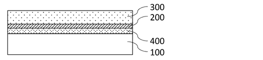
- FIG. 1 shows a substrate with a transparent electrode in which a base layer 200 is formed on a film substrate (hereinafter also referred to as a transparent film base material) 100 and a transparent electrode thin film 300 is formed on the base layer 200.
- the underlayer 200 and the transparent electrode thin film 300 are in contact with each other.
- the transparent electrode thin film 300 may have a plurality of layers such as layers 301 and 302.
- a coating layer 400 may be provided between the transparent film substrate 100 and the foundation layer 200.
- the coating layer 400 is provided for the purpose of protecting the transparent film substrate 100, suppressing the diffusion of low molecular weight components contained in the transparent film substrate 100, adjusting the optical film thickness, and the like.
- the coating layer 400 is formed only on one side of the transparent film substrate 100, but the coating layer may be formed on both sides.
- the transparent film constituting the transparent film substrate 100 is preferably transparent and colorless at least in the visible light region.
- the underlayer 200 contains indium oxide as a main component, and is dielectric and crystalline.
- the underlayer 200 may contain a metal oxide such as zinc oxide or yttrium oxide as a main component.
- “having a main component” a substance means that the content of the substance is 51% by weight or more, preferably 70% by weight or more, more preferably 90% by weight or more. As long as the function of the present invention is not impaired, each layer may contain components other than the main component.
- the content of indium oxide, zinc oxide or yttrium oxide in the underlayer 200 is preferably 87.5% by weight to 99.0% by weight, and more preferably 90% by weight to 95% by weight.
- the underlayer 200 may contain a doped impurity.
- a doped impurity is preferably tin oxide, zinc oxide, titanium oxide or tungsten oxide.
- the underlying layer is indium tin oxide (ITO)
- the doped impurity is zinc oxide
- the underlying layer is indium zinc oxide (IZO).
- the content of the doping impurity in the underlayer 200 is preferably 4.5% by weight to 12.5% by weight, and more preferably 5% by weight to 10% by weight.
- Indium oxide, zinc oxide, or yttrium oxide constituting the underlayer 200 not only controls the surface free energy of the underlayer 200 to an optimum value for forming the transparent electrode thin film 300, but also includes chemical factors such as water vapor. From the viewpoint of barrier properties that protect the film against physical factors such as plasma, it is also preferable because it does not contain carbon or nitrogen atoms that can inhibit crystallization of the transparent electrode thin film 300. Furthermore, indium oxide, zinc oxide, or yttrium oxide constituting the base layer 200 can suppress crystallization of the transparent electrode thin film 300 in a room temperature environment as compared with a base layer material such as silicon oxide. This is considered to be effective in controlling the activation energy when the transparent electrode thin film 300 is crystallized. Moreover, the above-mentioned material is preferable also from the point that a lattice matching with the transparent electrode thin film 300 becomes favorable.
- the underlayer 200 is preferably formed by a sputtering method.
- a base layer is formed by sputtering using silicon having a strong bond with oxygen, oxygen can easily become a supersaturated film, so that the crystallization of the transparent electrode thin film 300 formed thereon is excessively promoted and room temperature crystallization There is a risk of progress. Therefore, it is preferable that the underlayer does not substantially contain silicon oxide. Similarly, it is preferable that the underlayer contains substantially no cerium oxide.
- “substantially free” of a substance means that the content of the substance is less than 1% by weight, preferably less than 0.1% by weight, particularly preferably 0% by weight.
- the film thickness of the underlayer 200 is preferably 2 to 15 nm, more preferably 2 to 10 nm, still more preferably 2 to 5 nm, and particularly preferably 2.5 to 4 nm.
- diffusion suppression of crystallization-inhibiting components of the transparent electrode thin film 300 such as carbon atoms and nitrogen atoms from the transparent film substrate 100, and transparency from plasma when the transparent electrode thin film 300 is formed by a sputtering method are used.
- There are roles such as protection of the film substrate 100 and surface free energy control when the transparent electrode thin film 300 is formed, and the above-mentioned film thickness range is preferable in order to satisfy these roles.
- the underlayer 200 by reducing the thickness of the underlayer 200 to 2 to 5 nm (preferably 2.5 to 4 nm), the underlayer tends to be dielectric and crystalline, and promotes crystallization during heat treatment and under a normal temperature environment.
- the effect of suppressing crystallization can be suitably obtained.
- being a dielectric means that the resistivity is 1 ⁇ 10 2 ⁇ cm or more. If the underlayer is a conductor, it is considered that the free electrons in the underlayer and the free electrons in the transparent electrode thin film move, and the crystallization is promoted by the interaction between the electrons and the lattice. There is a risk of crystallization proceeding.
- crystalline means that which can confirm the crystal state of crystal grains and the like, and can confirm that it contains an atomic arrangement order by observation of a lattice image using a transmission electron microscope (TEM).
- TEM transmission electron microscope
- underlayer 200 By making the underlayer (hereinafter also referred to as a dielectric underlayer) 200 crystalline, not only the control of surface free energy and barrier characteristics, but also the underlayer 200 and the transparent layer when the transparent electrode thin film 300 is formed by sputtering. Crystal nuclei can be formed in the film thickness direction of the transparent electrode thin film 300 from the interface with the electrode thin film 300, and the crystal nuclei can promote crystallization during heat treatment.
- the transparent electrode thin film and the underlayer are different materials, it is easy to evaluate the physical properties from the surface of the underlayer by etching away the transparent electrode thin film. Also, when the underlying layer and transparent electrode thin film are the same material, considering the difference in crystallinity at the interface between them, measuring the etching rate reveals the surface of the underlying layer and evaluates the physical properties Is possible.
- the transparent electrode thin film 300 is amorphous.
- the transparent electrode thin film 300 is made of a transparent conductive oxide, and preferably contains indium oxide as a main component.
- the content of indium oxide in the transparent electrode thin film 300 is preferably 87.5% by weight to 99.0% by weight, and more preferably 90% by weight to 95% by weight.
- the transparent electrode thin film 300 preferably contains a doped impurity for imparting conductivity by providing a carrier density in the film.
- a doped impurity is preferably tin oxide, zinc oxide, titanium oxide or tungsten oxide.
- the transparent electrode thin film when the doped impurity is tin oxide is indium tin oxide (ITO), and the transparent electrode thin film when the doped impurity is zinc oxide is indium oxide zinc (IZO).
- the content of the doping impurity in the transparent electrode thin film 300 is preferably 4.5% by weight to 12.5% by weight, and more preferably 5% by weight to 10% by weight.
- the film thickness of the transparent electrode thin film 300 is preferably 15 nm to 30 nm, more preferably 17 nm to 27 nm, and further preferably 20 nm to 25 nm.
- the total thickness of the transparent electrode thin film 300 and the underlayer 200 is preferably less than 50 nm, more preferably 10 to 45 nm, and particularly preferably 20 to 30 nm.
- the transparent electrode thin film 300 preferably has low resistance particles.
- the low resistance particles are preferably transparent conductive oxide particles constituting the transparent electrode thin film 300.
- crystal nuclei can be formed in the thickness direction of the transparent electrode thin film from the interface between the base layer 200 and the transparent electrode thin film 300.
- the diameter of the low-resistance particles has a maximum value inside the film of the transparent electrode thin film.
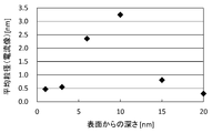
- FIG. 4 shows a profile of the average particle diameter of the low resistance particles in the film thickness direction of the transparent electrode thin film.
- the horizontal axis represents the depth of the transparent electrode thin film, where 0 nm is the surface of the transparent electrode thin film 300 and 20 nm is immediately above the interface between the transparent electrode thin film 300 and the dielectric underlayer 200.
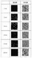
- the current images in FIGS. 5 and 6 are obtained by mapping current values when the surface is scanned using a conductive cantilever while applying a constant bias. Since the low resistance particles are observed as a high current region (white region of the current image in FIGS.
- the average particle diameter is obtained from the average value of the particle diameters r of all the low resistance particles in the current image.
- the present invention will be further described along with a method for producing a substrate with a transparent electrode.
- the transparent film base material 100 is used (base material preparation step).
- the transparent electrode thin film 300 is formed on the dielectric underlayer 200 (transparent electrode thin film forming step).
- the material of the transparent film constituting the transparent film substrate 100 is not particularly limited as long as it is colorless and transparent at least in the visible light region and has heat resistance at the formation temperature of the transparent electrode thin film.
- the transparent film material include polyester resins such as polyethylene terephthalate (PET), polybutylene terephthalate (PBT), and polyethylene naphthalate (PEN), cycloolefin resins, polycarbonate resins, polyimide resins, and cellulose resins. Can be mentioned. Of these, polyester resins are preferable, and polyethylene terephthalate is particularly preferably used.
- the thickness of the transparent film substrate 100 is not particularly limited, but is preferably 10 ⁇ m to 400 ⁇ m, and more preferably 20 ⁇ m to 200 ⁇ m. If the thickness is within the above range, the transparent film substrate 100 may have durability and appropriate flexibility, so that the dielectric underlayer 200 and the transparent electrode thin film 300 are formed thereon by a roll-to-roll method. It is possible to form a film with high productivity.
- a material having improved mechanical properties such as Young's modulus and heat resistance by orienting molecules by biaxial stretching is preferably used.
- a stretched film has a property of being thermally contracted when heated because strain caused by stretching remains in the molecular chain.
- stress is relaxed by adjusting the stretching conditions and heating after stretching, the thermal shrinkage rate is reduced to about 0.2% or less, and the heat shrink start temperature is increased.
- Biaxially stretched films low heat shrink films
- a coating layer (functional layer) 400 such as a hard coat layer may be formed on one side or both sides of the transparent film substrate 100.
- the thickness of the coating layer is preferably 1 to 10 ⁇ m, more preferably 3 to 8 ⁇ m, and even more preferably 5 to 8 ⁇ m.
- the material of the coating layer is not particularly limited, and a material obtained by applying and curing a urethane resin, an acrylic resin, a silicone resin, or the like can be appropriately used.
- the formation method of the dielectric underlayer 200 is preferably a sputtering method from the viewpoint of productivity, and the magnetron sputtering method is particularly preferable.
- Sputter deposition is performed while a carrier gas containing an inert gas such as argon or nitrogen and an oxygen gas is introduced into a deposition chamber (chamber).
- the introduced gas is preferably a mixed gas of argon and oxygen.
- Argon and oxygen may be prepared in advance with a gas having a predetermined mixing ratio, or each gas may be mixed after the flow rate is controlled by a flow rate control device (mass flow controller).
- the mixed gas may contain other gases as long as the function of the present invention is not impaired.
- the pressure (total pressure) in the film forming chamber is preferably 0.1 Pa to 1.0 Pa, and more preferably 0.15 Pa to 0.8 Pa.
- the magnet strength during magnetron sputtering is preferably 700 to 1300 gauss, thereby suppressing a decrease in the utilization efficiency of the sputter target due to extreme erosion, and forming a good underlayer 200. .
- the power source used for sputtering is not limited, and a DC power source, an AC power source, or the like can be selected according to the target material.
- the discharge voltage depends on the type of the device and the power source, it is preferably about ⁇ 100 to ⁇ 350 V, more preferably about ⁇ 180 to ⁇ 300 V in order to form a good underlayer 200.
- the underlayer 200 is preferably formed with as little damage as possible to the substrate.
- damage to the substrate can be reduced by a technique such as film formation at a low power density.
- the amount of oxygen introduced into the sputtering chamber is important.
- the above-described dielectric underlayer can be formed by forming a film while introducing oxygen more than three times more than the amount of oxygen introduced when forming normal transparent conductive indium oxide (so-called bottom oxygen amount). It becomes possible. Even if conductive carriers due to oxygen vacancies are generated by performing sputter deposition under an excessive oxygen supply, the carrier density is reduced so as not to conduct electricity, and the extremes due to the barrier height of the crystal grain boundaries. It is considered that dielectric indium oxide is formed due to the decrease in mobility.
- the amount of oxygen introduced during the formation of the dielectric underlayer is preferably 3 to 8 times the amount of bottom oxygen. If the amount of oxygen is too large, there is a possibility that the film-forming speed is lowered or the thin film is damaged by oxygen plasma.
- the oxygen partial pressure in the film forming chamber when forming the dielectric underlayer 200 is preferably 1 ⁇ 10 ⁇ 2 Pa to 4 ⁇ 10 ⁇ 1 Pa, and preferably 2.5 ⁇ 10 ⁇ 2 Pa to 2.0 ⁇ 10. More preferably, it is ⁇ 1 Pa.
- the film thickness of the underlayer 200 is considered to contribute to the formation of the dielectric.
- the underlayer 200 having a desired resistivity is preferable by setting the thickness of the underlayer 200 to 2 to 5 nm (preferably 2.5 to 4 nm). Can be formed.
- the electric power for forming the dielectric base layer 200 is not particularly limited, but is preferably 1 to 5 kW, and more preferably 2 to 4 kW.
- the film forming conditions such as the amount of oxygen, power, and pressure when forming the base layer 200, the base layer 200 can be made not only dielectric but also crystalline.
- the method for forming the transparent electrode thin film 300 is preferably a sputtering method from the viewpoint of productivity, and among these, a magnetron sputtering method is preferable.
- the oxygen partial pressure in the deposition chamber when forming the transparent electrode thin film 300 is preferably 1 ⁇ 10 ⁇ 3 Pa to 5 ⁇ 10 ⁇ 2 Pa, and preferably 3.0 ⁇ 10 ⁇ 3 Pa to 4.0 ⁇ 10 ⁇ . More preferably, it is 2 Pa.
- the oxygen partial pressure range is a value lower than the oxygen partial pressure in a general ITO film formed by sputtering. That is, the transparent electrode thin film is formed with a small amount of oxygen supply. Therefore, it is considered that many oxygen vacancies exist in the amorphous transparent electrode thin film after film formation.
- the formation of the transparent electrode thin film 300 by the sputtering method may form the entire desired film thickness by one film formation, but from the viewpoint of the production processing speed and the heat history to the transparent film substrate 100, It is preferable to form by multiple times of lamination.
- crystallinity can be controlled by the following two methods. One is a method of changing the film forming conditions for each layer using a target having the same composition, and the other is a method of stacking using a target having a different composition.
- the former method for example, when a film is formed on the dielectric underlayer 200, crystallization is activated by accelerating the formation of crystal nuclei by setting the applied power high or by setting the applied voltage low. It is possible to increase the energy.
- the segregation of the dopant contained in the transparent electrode thin film to the surface of the transparent electrode thin film 300 can be suppressed by adjusting the applied power and the partial pressure of the reactive gas (oxygen, etc.) during the outermost film formation. Uniform crystallization is possible in the transparent electrode thin film.
- the latter method is a method in which the material constituting the transparent electrode thin film and the composition / concentration of the dopant are sequentially changed. In the case of this method, from the viewpoint of smooth electron transport in the transparent electrode thin film, it is preferable that the dopant materials are the same, and the change in concentration preferably occurs only in the film thickness direction.
- the power for forming the transparent electrode thin film 300 is not particularly limited, but is preferably 9 to 15 kW, and more preferably 10 to 13 kW.
- the power when forming the transparent electrode thin film (layer 301 in FIG. 2) on the base layer 200 side is preferably 9 to 15 kW, more preferably 10 to 13 kW.
- the power for forming the transparent electrode thin film (layer 302 in FIG. 2) is preferably 1 to 5 kW, more preferably 2 to 4 kW.
- the substrate temperature at the time of forming the underlayer and the transparent electrode thin film may be in a range in which the transparent film substrate has heat resistance, and is preferably 60 ° C. or lower.
- the substrate temperature is more preferably ⁇ 20 ° C. to 40 ° C.
- the underlayer and the transparent electrode thin film are formed by a roll-to-roll method using a winding type sputtering apparatus.
- a roll-to-roll method By forming the film by a roll-to-roll method, a roll-shaped wound body of a long sheet of a transparent film substrate on which an amorphous transparent electrode thin film is formed is obtained.
- the dielectric base layer 200 and the transparent electrode thin film 300 may be continuously formed using a winding type sputtering apparatus.
- a method of degassing the film roll in the sputtering apparatus or before the apparatus is generally used.
- moisture can be removed by heating.
- the dielectric underlayer of the present invention it is possible to suppress the diffusion of the components from the film during the formation of the transparent electrode, and to suppress the diffusion after the film formation.
- a substrate with a transparent electrode can be produced.
- substrate with a transparent electrode may be used for the crystallization process (crystallization process).
- crystallization process crystallizing the amorphous transparent electrode thin film 300, a low resistance transparent electrode thin film can be obtained.
- the substrate with a transparent electrode is preferably heated to 120 to 170 ° C.
- the crystallization is preferably performed in an oxygen-containing atmosphere such as the air. Crystallization proceeds even in a vacuum or in an inert gas atmosphere, but in a low oxygen concentration atmosphere, crystallization tends to take a longer time than in an oxygen atmosphere.
- crystallization may be performed with the wound body as it is, and crystallization is performed while the film is conveyed by a roll-to-roll.
- the film may be cut into a predetermined size and crystallized.
- the substrate after forming the transparent electrode thin film may be cured (standing) in a heating chamber or the like.
- crystallization is performed by roll-to-roll, the substrate is introduced into a heating furnace while being conveyed and heated, and then wound again in a roll shape.
- the transparent electrode thin film 300 after the crystallization step preferably has a crystallinity of 80% or more, and more preferably 90% or more.
- the crystallinity is obtained from the ratio of the area occupied by the crystal grains in the observation field during microscopic observation.
- the transparent electrode thin film 300 after the crystallization step preferably has a resistivity of 3.5 ⁇ 10 ⁇ 4 ⁇ cm or less.
- the surface resistance of the transparent electrode thin film 300 after the crystallization step is preferably 170 ⁇ / ⁇ or less, and more preferably 150 ⁇ / ⁇ or less. If the transparent electrode thin film has a low resistance, it can contribute to improving the response speed of the capacitive touch panel, improving the uniformity of in-plane luminance of organic EL lighting, and reducing the power consumption of various optical devices.
- the carrier density of the transparent electrode thin film 300 after the crystallization process is preferably 4 ⁇ 10 20 cm ⁇ 3 to 9 ⁇ 10 20 cm ⁇ 3 , and 6 ⁇ 10 20 cm ⁇ 3 to 8 ⁇ 10 20 cm ⁇ 3. It is more preferable that If the carrier density is within the above range, the resistance of the transparent electrode thin film 300 can be reduced.
- the underlayer is made of a dielectric and crystalline so that “crystallization promotion during heat treatment” and “crystallization suppression in a room temperature environment” Can be achieved at the same time.
- the main component of the base layer is indium oxide, so that the base layer of another metal oxide (for example, zinc oxide or yttrium oxide) is formed, Crystallization of the transparent electrode thin film in a room temperature environment can be further suppressed.
- indium oxide as the main component of the underlayer, good adhesion to electrode materials constituting conductive pastes, etc., which will be described later, and optical materials constituting optical adhesive sheets (OCA), etc. Can be.
- substrate with a transparent electrode of this invention can be used as transparent electrodes, such as a display, a light emitting element, a photoelectric conversion element, and is used suitably as a transparent electrode for touchscreens.
- a transparent electrode thin film is low resistance, it is preferably used for a capacitive touch panel.
- a conductive ink or paste is applied on a substrate with a transparent electrode, and heat treatment is performed, whereby a collecting electrode as a wiring for a routing circuit is formed.
- the method for the heat treatment is not particularly limited, and examples thereof include a heating method using an oven or an IR heater.
- the temperature and time of the heat treatment are appropriately set in consideration of the temperature and time at which the conductive paste adheres to the transparent electrode. For example, examples include heating at 120 to 150 ° C. for 30 to 60 minutes for heating by an oven and heating at 150 ° C. for 5 minutes for heating by an IR heater.
- the formation method of the circuit wiring is not limited to the above, and may be formed by a dry coating method.
- the wiring for the routing circuit is formed by photolithography, the wiring can be thinned.
- the film thickness of the underlayer and the transparent electrode thin film values obtained by observation with a transmission electron microscope (TEM) of the cross section of the substrate with the transparent electrode were used.
- the surface resistance of the transparent electrode thin film was measured by four-probe pressure contact measurement using a low resistivity meter Loresta GP (MCP-T710, manufactured by Mitsubishi Chemical Corporation).
- AFM measurement was performed in a measurement range of 1 micron square using NanoNavi II manufactured by SII.
- the bias voltage during current image measurement was 1V.
- Example A1 By the following method, the base layer and the transparent electrode thin film were continuously formed on the transparent film substrate using a winding type sputtering apparatus.
- a base layer was formed by sputtering on one surface of a 188 ⁇ m thick PET film having hard coat layers made of urethane resin formed on both surfaces.
- indium tin oxide titanium oxide content: 10% by weight
- the partial pressure of oxygen was 1.0 ⁇ 10 ⁇ 1 Pa
- the pressure in the film forming chamber was 0.1.
- Film formation was performed under the conditions of 2 Pa, a substrate temperature of 0 ° C., and a power of 2 kW.
- the film thickness was 3 nm.
- Transparent electrode thin film formation A transparent electrode thin film was formed on the underlayer to produce a substrate with a transparent electrode.
- indium tin oxide titanium oxide content of 10% by weight
- the partial pressure of oxygen was 3.3 ⁇ 10 ⁇ 2 Pa
- the pressure in the film forming chamber was 0.1.
- Film formation was performed under the conditions of 2 Pa, a substrate temperature of 0 ° C., and a power of 12 kW.
- the film thickness was 22 nm.
- Example A2 Example A3, Comparative Example 1 and Comparative Example 3
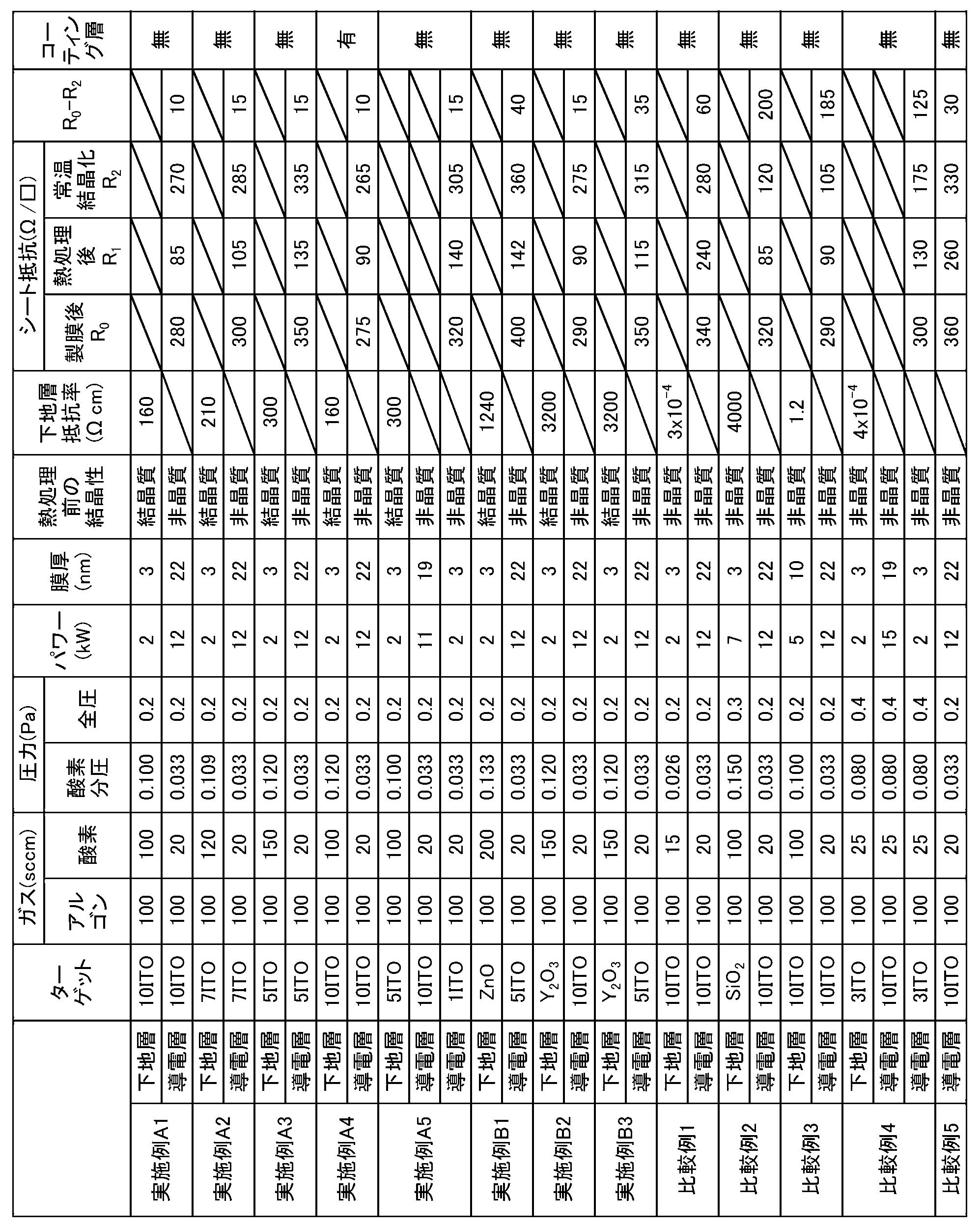
- Example A1 film formation and crystallization were performed by changing the film formation conditions of the base layer and the transparent electrode thin film as shown in Table 1.
- Example A4 In Example A4, as shown in FIG. 3, the coating layer 400 was formed on the transparent film substrate 100.
- the coating layer 400 was formed as follows. Acrylic resin (trade name: Dianar BR-102, manufactured by Mitsubishi Rayon) was dissolved in methyl cellosolve. The solid content concentration was 30% by weight. To this resin solution, zirconium oxide (trade name: zirconia particles TZ-3Y-E, manufactured by Tosoh Corporation) was added in an amount of 1% by weight with respect to the acrylic resin and stirred sufficiently to prepare a coating solution. This coating solution was applied to a thickness of 3 ⁇ m by a bar coating method and dried at 125 ° C. for 15 minutes to form a 1 ⁇ m-thick resin layer. On the surface of the transparent film substrate 100 on which the coating layer 400 was formed, a base layer and a transparent electrode thin film were formed in the same manner as in Example A1, and then crystallization was performed.
- Acrylic resin trade name: Dianar BR-102, manufactured by Mitsubishi Rayon
- Example A5 and Comparative Example 4 As shown in FIG. 2, a two-layer transparent electrode thin film was formed. The conditions for forming the underlayer and the transparent electrode thin film are shown in Table 1. Otherwise, the underlayer and the transparent electrode thin film were formed and crystallized in the same manner as in Example A1.
- Example B1, Example B2, Example B3 and Comparative Example 2 film formation and crystallization were carried out by changing the target type and film formation conditions during film formation of the underlayer and the transparent electrode thin film as shown in Table 1.
- zinc oxide oxygen (ZnO 0.5 ) with less oxygen than stoichiometric zinc oxide (ZnO) was used.
- yttrium oxide oxygen (Y 2 O 2.5 ) with less oxygen than stoichiometric yttrium oxide (Y 2 O 3 ) was used.
- Example 5 The underlying layer was not formed, and a transparent electrode thin film was formed on one surface of the PET film by sputtering. Otherwise, crystallization was performed in the same manner as in Example A1.
- Table 1 shows the configuration, film forming conditions, and characteristics of each layer of each example and comparative example.
- Example B1 Example B1, Comparative Example 1 and Comparative Examples 3 to 5
- An AC power source MF power source
- a DC power source was used for forming the transparent electrode thin film 300.
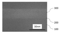
- FIG. 7 shows a cross-sectional image of a transmission electron microscope (TEM) in Example A1.
- the transparent electrode thin film 300 is formed on the underlayer 200, and it can be determined from the image contrast that the underlayer 200 of Example A1 is crystalline.
- FIG. 8 shows a cross-sectional image of a transmission electron microscope (TEM) in Comparative Example 1. Since the contrast of the image is not confirmed near the interface between the foundation layer 200 and the transparent electrode thin film 300, it can be determined that the foundation layer 200 of Comparative Example 1 is amorphous.
- TEM transmission electron microscope
- Example A1 to Example A5 in which the main component of the underlayer is indium oxide, suppresses room temperature crystallization compared to Examples B1 to B3 in which the main component of the underlayer is zinc oxide or yttrium oxide. It is thought that the effect can be enhanced.
- a dielectric indium oxide thin film can be formed by forming the underlayer with a high oxygen partial pressure.
- the oxygen partial pressure during film formation of the underlayer is high as in Comparative Example 3, the underlayer cannot be made a dielectric depending on the film thickness and film formation power.
Landscapes
- Chemical & Material Sciences (AREA)
- Engineering & Computer Science (AREA)
- Chemical Kinetics & Catalysis (AREA)
- Materials Engineering (AREA)
- Mechanical Engineering (AREA)
- Metallurgy (AREA)
- Organic Chemistry (AREA)
- Physics & Mathematics (AREA)
- Theoretical Computer Science (AREA)
- General Engineering & Computer Science (AREA)
- Thermal Sciences (AREA)
- Human Computer Interaction (AREA)
- General Physics & Mathematics (AREA)
- Non-Insulated Conductors (AREA)
- Physical Vapour Deposition (AREA)
- Life Sciences & Earth Sciences (AREA)
- Sustainable Development (AREA)
- Sustainable Energy (AREA)
- Manufacturing Of Electric Cables (AREA)
- Laminated Bodies (AREA)
- Photovoltaic Devices (AREA)
Abstract
Description
図1は、フィルム基板(以下、透明フィルム基材ともいう)100上に下地層200が形成され、下地層200上に透明電極薄膜300が形成された透明電極付き基板を示している。下地層200と透明電極薄膜300とは接している。図2に示すように、透明電極薄膜300は、層301,302のような複数層の構成でもよい。図3に示すように、透明フィルム基材100と下地層200との間にコーティング層400が設けられていてもよい。コーティング層400は、透明フィルム基材100の保護や、透明フィルム基材100中に含まれる低分子量成分の拡散抑制、光学膜厚調整等を目的として設けられる。図3ではコーティング層400が透明フィルム基材100の片面にのみ形成されているが、両面にコーティング層が形成されていてもよい。
以下、透明電極付き基板の製造方法に沿って、本発明をさらに説明する。上記の透明電極付き基板の製造方法では、透明フィルム基材100が用いられる(基材準備工程)。透明フィルム基材100上に誘電体下地層200が形成された後(下地層形成工程)、誘電体下地層200上に透明電極薄膜300が形成される(透明電極薄膜形成工程)。
透明フィルム基材100を構成する透明フィルムは、少なくとも可視光領域で無色透明であり、透明電極薄膜の形成温度における耐熱性を有していれば、その材料は特に限定されない。透明フィルムの材料としては、ポリエチレンテレフタレート(PET)、ポリブチレンテレフテレート(PBT)、ポリエチレンナフタレート(PEN)等のポリエステル系樹脂、シクロオレフィン系樹脂、ポリカーボネート樹脂、ポリイミド樹脂、セルロース系樹脂等が挙げられる。中でも、ポリエステル系樹脂が好ましく、ポリエチレンテレフタレートが特に好ましく用いられる。
誘電体下地層200の形成方法は、生産性の観点からスパッタリング法が好ましく、中でもマグネトロンスパッタリング法が好ましい。スパッタ製膜は、製膜室(チャンバー)内に、アルゴンや窒素等の不活性ガスおよび酸素ガスを含むキャリアガスが導入されながら行われる。導入ガスは、アルゴンと酸素の混合ガスが好ましい。アルゴンと酸素は、所定の混合比のガスを予め用意してもよいし、それぞれのガスを流量制御装置(マスフローコントローラ)により流量を制御した後に混合してもよい。なお、混合ガスには、本発明の機能を損なわない限りにおいて、その他のガスが含まれていてもよい。製膜室内の圧力(全圧)は、0.1Pa~1.0Paが好ましく、0.15Pa~0.8Paがより好ましい。
透明電極薄膜300の形成方法は、生産性の観点からスパッタリング法が好ましく、中でもマグネトロンスパッタリング法が好ましい。
結晶化工程では、透明電極付き基板が120~170℃に加熱されることが好ましい。
膜中に酸素を十分に取り込み、結晶化時間を短縮するためには、結晶化は大気中等の酸素含有雰囲気下で行われることが好ましい。真空中や不活性ガス雰囲気下でも結晶化は進行するが、低酸素濃度雰囲気下では、酸素雰囲気下に比べて結晶化に長時間を要する傾向がある。
本発明の透明電極付き基板は、ディスプレイや発光素子、光電変換素子等の透明電極として用いることができ、タッチパネル用の透明電極として好適に用いられる。中でも、透明電極薄膜が低抵抗であることから、静電容量方式タッチパネルに好ましく用いられる。
以下の方法により、透明フィルム基材上に、下地層および透明電極薄膜が、巻取式スパッタリング装置を用いて連続して製膜された。
ウレタン系樹脂からなるハードコート層が両面に形成された厚み188μmのPETフィルムの一方の面上に、スパッタリング法により下地層を形成した。酸化インジウム・スズ(酸化スズ含有量10重量%)をターゲットとして用い、酸素とアルゴンの混合ガスを装置内に導入しながら、酸素分圧1.0×10⁻¹Pa、製膜室内圧力0.2Pa、基板温度0℃、パワー2kWの条件で製膜を行った。膜厚は3nmであった。
下地層上に透明電極薄膜を形成し、透明電極付き基板を作製した。酸化インジウム・スズ(酸化スズ含有量10重量%)をターゲットとして用い、酸素とアルゴンの混合ガスを装置内に導入しながら、酸素分圧3.3×10⁻²Pa、製膜室内圧力0.2Pa、基板温度0℃、パワー12kWの条件で製膜を行った。膜厚は22nmであった。
この透明電極付き基板を、150℃で1時間熱処理を行った。顕微鏡観察によってほぼ完全に結晶化されていることが確認された(結晶化度100%)。
別途、下地層のみの製膜を行い、表面の抵抗測定の結果から抵抗率を算出したところ、1.6×10²Ωcmであった。また、AFMを用いて1μm四方の形状測定を行い、形状から結晶粒の存在を確認し、TEMによる格子像観察から、5nm以上の短距離の秩序を確認した。
製膜したフィルムを、25℃・50%RHの環境に1週間放置し、その時のシート抵抗を測定することで評価した。シート抵抗が低下していることと結晶化が進んでいることとを等価とした。
上記実施例A1において、下地層および透明電極薄膜の製膜条件を表1に示すように変更して、製膜および結晶化が行われた。表1中、nITO(n=1,3,5,7,10)は、酸化スズをn重量%含有する酸化インジウムを意味する(以下の実施例および比較例においても同じ)。
実施例A4では、図3に示すように、透明フィルム基材100上にコーティング層400を形成した。コーティング層400は、以下のように形成した。アクリル樹脂(商品名:ダイヤナールBR-102、三菱レイヨン製)をメチルセロソルブに溶解した。固形分濃度は30重量%とした。この樹脂溶液に、酸化ジルコニウム(商品名:ジルコニア粒子TZ-3Y-E、東ソー製)を、アクリル樹脂に対して1重量%添加して十分に撹拌することで、塗布液を作製した。この塗布液をバーコート法により、3μmの厚みに塗布し、125℃で15分間乾燥させることで、1μm厚の樹脂層を形成した。透明フィルム基材100のコーティング層400形成面上に、実施例A1と同様にして、下地層および透明電極薄膜の製膜が行われ、その後、結晶化が行われた。
図2に示すように2層の透明電極薄膜を形成した。下地層および透明電極薄膜の製膜条件を表1に示す。それ以外は、実施例A1と同様にして、下地層および透明電極薄膜の製膜および結晶化が行われた。
上記実施例A1において、下地層および透明電極薄膜の製膜時のターゲットの種類および製膜条件を表1に示すように変更して、製膜および結晶化が行われた。酸化亜鉛は、化学量論的な酸化亜鉛(ZnO)よりも酸素を少なくしたもの(ZnO0.5)を用いた。酸化イットリウムは、化学量論的な酸化イットリウム(Y2O3)よりも酸素を少なくしたもの(Y2O2.5)を用いた。
下地層が製膜されず、PETフィルムの一方の面上に、スパッタリング法により透明電極薄膜が形成された。それ以外は、実施例A1と同様にして、結晶化が行われた。
200:誘電体下地層(下地層)
300:透明電極薄膜
400:コーティング層
Claims (11)
- フィルム基板上に、透明導電性酸化物からなる透明電極薄膜が形成された透明電極付き基板であって、
前記フィルム基板と前記透明電極薄膜との間には、酸化インジウムを主成分として含有する下地層が形成されており、
前記下地層と前記透明電極薄膜とは接しており、
前記透明電極薄膜は非晶質であり、
前記下地層は誘電体かつ結晶質である、透明電極付き基板。 - 前記下地層の膜厚が2~15nmである、請求項1に記載の透明電極付き基板。
- 前記透明電極薄膜は、酸化インジウムを主成分として含有する、請求項1または2に記載の透明電極付き基板。
- 前記透明電極薄膜の膜厚が15~30nmである、請求項1~3のいずれか1項に記載の透明電極付き基板。
- 前記透明電極薄膜は低抵抗粒子を有しており、原子間力顕微鏡を用いた電流像測定により求められる前記低抵抗粒子の径が、前記透明電極薄膜の膜内部で最大値を示す、請求項1~4のいずれか1項に記載の透明電極付き基板。
- 請求項1~5のいずれか1項に記載の透明電極付き基板の製造方法であって、
前記下地層および前記透明電極薄膜は、いずれも酸素ガスを用いてマグネトロンスパッタリング法で製膜され、かつ、前記下地層の製膜時にチャンバー内に導入する酸素量は、前記透明電極薄膜の製膜時にチャンバー内に導入する酸素量の3倍以上である、透明電極付き基板の製造方法。 - フィルム基板上に、透明導電性酸化物からなる透明電極薄膜が形成された透明電極付き基板であって、
前記フィルム基板と前記透明電極薄膜との間には、金属酸化物を主成分として含有する下地層が形成されており、
前記下地層と前記透明電極薄膜とは接しており、
前記透明電極薄膜は非晶質であり、
前記下地層は誘電体かつ結晶質であり、前記下地層の膜厚が2~15nmである、透明電極付き基板。 - 前記金属酸化物は、酸化亜鉛である、請求項7に記載の透明電極付き基板。
- 前記金属酸化物は、酸化イットリウムである、請求項7に記載の透明電極付き基板。
- 前記透明電極薄膜は、酸化インジウムを主成分として含有する、請求項7~9のいずれか1項に記載の透明電極付き基板。
- 前記下地層の膜厚が2~5nmである、請求項7~10のいずれか1項に記載の透明電極付き基板。
Priority Applications (4)
| Application Number | Priority Date | Filing Date | Title |
|---|---|---|---|
| CN201580003181.6A CN105830173B (zh) | 2014-01-28 | 2015-01-19 | 带有透明电极的基板及其制造方法 |
| US15/114,639 US10270010B2 (en) | 2014-01-28 | 2015-01-19 | Substrate with transparent electrode and method for producing same |
| JP2015559875A JP6419091B2 (ja) | 2014-01-28 | 2015-01-19 | 透明電極付き基板およびその製造方法 |
| US16/294,100 US10777709B2 (en) | 2014-01-28 | 2019-03-06 | Substrate with transparent electrode and method for producing same |
Applications Claiming Priority (2)
| Application Number | Priority Date | Filing Date | Title |
|---|---|---|---|
| JP2014013603 | 2014-01-28 | ||
| JP2014-013603 | 2014-01-28 |
Related Child Applications (2)
| Application Number | Title | Priority Date | Filing Date |
|---|---|---|---|
| US15/114,639 A-371-Of-International US10270010B2 (en) | 2014-01-28 | 2015-01-19 | Substrate with transparent electrode and method for producing same |
| US16/294,100 Continuation US10777709B2 (en) | 2014-01-28 | 2019-03-06 | Substrate with transparent electrode and method for producing same |
Publications (1)
| Publication Number | Publication Date |
|---|---|
| WO2015115237A1 true WO2015115237A1 (ja) | 2015-08-06 |
Family
ID=53756814
Family Applications (1)
| Application Number | Title | Priority Date | Filing Date |
|---|---|---|---|
| PCT/JP2015/051286 Ceased WO2015115237A1 (ja) | 2014-01-28 | 2015-01-19 | 透明電極付き基板およびその製造方法 |
Country Status (5)
| Country | Link |
|---|---|
| US (2) | US10270010B2 (ja) |
| JP (1) | JP6419091B2 (ja) |
| CN (1) | CN105830173B (ja) |
| TW (1) | TWI651208B (ja) |
| WO (1) | WO2015115237A1 (ja) |
Cited By (7)
| Publication number | Priority date | Publication date | Assignee | Title |
|---|---|---|---|---|
| CN106598317A (zh) * | 2015-10-20 | 2017-04-26 | 深圳莱宝高科技股份有限公司 | 一种触控面板及其制作方法 |
| CN107329635A (zh) * | 2016-04-28 | 2017-11-07 | 宸美(厦门)光电有限公司 | 导电结构及触控面板 |
| WO2020026606A1 (ja) * | 2018-08-01 | 2020-02-06 | 株式会社カネカ | 透明電極付き基板およびその製造方法 |
| WO2020189229A1 (ja) * | 2019-03-20 | 2020-09-24 | 株式会社カネカ | 透明電極付き基板の製造方法 |
| WO2021020457A1 (ja) * | 2019-07-31 | 2021-02-04 | Agc株式会社 | 光学層、太陽電池モジュール、建築用外壁材及び建造物 |
| WO2021240962A1 (ja) * | 2020-05-25 | 2021-12-02 | 日東電工株式会社 | 光透過性導電性シートの製造方法 |
| US12156330B2 (en) | 2020-03-19 | 2024-11-26 | Nitto Denko Corporation | Light-transmitting electroconductive film and transparent electroconductive film |
Families Citing this family (6)
| Publication number | Priority date | Publication date | Assignee | Title |
|---|---|---|---|---|
| CN109642307B (zh) * | 2016-09-12 | 2020-04-10 | 株式会社爱发科 | 带透明导电膜的基板的制造方法、带透明导电膜的基板的制造装置及带透明导电膜的基板 |
| CN106847942B (zh) * | 2017-02-20 | 2018-05-25 | 江西师范大学 | 一种透明电极及其制备方法 |
| JP6782211B2 (ja) * | 2017-09-08 | 2020-11-11 | 株式会社東芝 | 透明電極、それを用いた素子、および素子の製造方法 |
| FR3071514B1 (fr) * | 2017-09-26 | 2019-11-01 | Commissariat A L'energie Atomique Et Aux Energies Alternatives | Procede de fabrication par pulverisation cathodique magnetron d'un electrolyte pour cellules electrochimiques a oxyde solide |
| JP7214592B2 (ja) * | 2019-08-05 | 2023-01-30 | 信越化学工業株式会社 | オルガノハイドロジェンポリシロキサンのエマルション、及びこれを用いた付加硬化型シリコーンエマルション組成物 |
| EP4600409A1 (en) * | 2022-10-05 | 2025-08-13 | Shincron Co., Ltd. | Homoepitaxial thin film, and manufacturing method and manufacturing apparatus thereof |
Citations (6)
| Publication number | Priority date | Publication date | Assignee | Title |
|---|---|---|---|---|
| US4605565A (en) * | 1982-12-09 | 1986-08-12 | Energy Conversion Devices, Inc. | Method of depositing a highly conductive, highly transmissive film |
| JP2000111930A (ja) * | 1998-09-30 | 2000-04-21 | Nippon Sheet Glass Co Ltd | Ito透明導電膜付き基板およびその製造方法 |
| JP2001265251A (ja) * | 2000-03-17 | 2001-09-28 | Minolta Co Ltd | 表示素子及び積層型表示素子 |
| WO2006019184A1 (ja) * | 2004-08-20 | 2006-02-23 | Teijin Limited | 透明導電性積層体および透明タッチパネル |
| WO2007058066A1 (ja) * | 2005-11-21 | 2007-05-24 | Idemitsu Kosan Co., Ltd. | 透明導電膜並びにそれを用いた基板、電子機器及び液晶表示装置 |
| WO2009011232A1 (ja) * | 2007-07-13 | 2009-01-22 | Nippon Mining & Metals Co., Ltd. | 複合酸化物焼結体、アモルファス複合酸化膜の製造方法、アモルファス複合酸化膜、結晶質複合酸化膜の製造方法及び結晶質複合酸化膜 |
Family Cites Families (18)
| Publication number | Priority date | Publication date | Assignee | Title |
|---|---|---|---|---|
| US4977013A (en) | 1988-06-03 | 1990-12-11 | Andus Corporation | Tranparent conductive coatings |
| JP3214586B2 (ja) | 1993-12-24 | 2001-10-02 | 東洋紡績株式会社 | 透明導電フィルム及びその製造方法 |
| TWI417905B (zh) * | 2004-09-13 | 2013-12-01 | 住友金屬鑛山股份有限公司 | A transparent conductive film and a method for manufacturing the same, and a transparent conductive substrate and a light-emitting device |
| KR101000057B1 (ko) | 2008-02-04 | 2010-12-10 | 엘지전자 주식회사 | 다층 투명전도층을 구비한 태양전지 이의 제조방법 |
| JP4687733B2 (ja) | 2008-03-14 | 2011-05-25 | 住友金属鉱山株式会社 | 透明電極、透明導電性基板および透明タッチパネル |
| EP2416253B1 (en) * | 2009-03-31 | 2014-07-23 | Fujitsu Limited | Data transmission circuit and data transmission method |
| JP2011003456A (ja) | 2009-06-19 | 2011-01-06 | Bridgestone Corp | 透明導電膜、透明導電性フィルムおよび透明導電膜の製造方法、並びに透明導電膜を用いたフレキシブルディスプレイ装置 |
| JP5101719B2 (ja) * | 2010-11-05 | 2012-12-19 | 日東電工株式会社 | 透明導電性フィルム、その製造方法及びそれを備えたタッチパネル |
| JP5122670B2 (ja) | 2010-11-05 | 2013-01-16 | 日東電工株式会社 | 透明導電性フィルムの製造方法 |
| JP5543907B2 (ja) | 2010-12-24 | 2014-07-09 | 日東電工株式会社 | 透明導電性フィルムおよびその製造方法 |
| FR2970110B1 (fr) * | 2010-12-29 | 2013-09-06 | St Microelectronics Crolles 2 | Procede de fabrication d'une couche de dielectrique polycristalline |
| JP5589855B2 (ja) | 2011-01-07 | 2014-09-17 | 日産自動車株式会社 | 操舵反力制御装置 |
| JP2012219301A (ja) * | 2011-04-06 | 2012-11-12 | Panasonic Corp | 結晶性ito膜およびその製造方法ならびに太陽電池 |
| CN202167550U (zh) * | 2011-06-29 | 2012-03-14 | 比亚迪股份有限公司 | 一种电池盖板组件及电池 |
| JP5833863B2 (ja) * | 2011-08-24 | 2015-12-16 | 日東電工株式会社 | 透明導電性フィルムおよびその製造方法 |
| CN104067353B (zh) | 2012-01-27 | 2016-10-26 | 株式会社钟化 | 带有透明电极的基板及其制造方法 |
| JP2013247075A (ja) * | 2012-05-29 | 2013-12-09 | Kitagawa Ind Co Ltd | 透明導電フィルム及びその製造方法 |
| JP6261988B2 (ja) * | 2013-01-16 | 2018-01-17 | 日東電工株式会社 | 透明導電フィルムおよびその製造方法 |
-
2015
- 2015-01-19 US US15/114,639 patent/US10270010B2/en active Active
- 2015-01-19 JP JP2015559875A patent/JP6419091B2/ja active Active
- 2015-01-19 WO PCT/JP2015/051286 patent/WO2015115237A1/ja not_active Ceased
- 2015-01-19 CN CN201580003181.6A patent/CN105830173B/zh active Active
- 2015-01-27 TW TW104102642A patent/TWI651208B/zh active
-
2019
- 2019-03-06 US US16/294,100 patent/US10777709B2/en active Active
Patent Citations (6)
| Publication number | Priority date | Publication date | Assignee | Title |
|---|---|---|---|---|
| US4605565A (en) * | 1982-12-09 | 1986-08-12 | Energy Conversion Devices, Inc. | Method of depositing a highly conductive, highly transmissive film |
| JP2000111930A (ja) * | 1998-09-30 | 2000-04-21 | Nippon Sheet Glass Co Ltd | Ito透明導電膜付き基板およびその製造方法 |
| JP2001265251A (ja) * | 2000-03-17 | 2001-09-28 | Minolta Co Ltd | 表示素子及び積層型表示素子 |
| WO2006019184A1 (ja) * | 2004-08-20 | 2006-02-23 | Teijin Limited | 透明導電性積層体および透明タッチパネル |
| WO2007058066A1 (ja) * | 2005-11-21 | 2007-05-24 | Idemitsu Kosan Co., Ltd. | 透明導電膜並びにそれを用いた基板、電子機器及び液晶表示装置 |
| WO2009011232A1 (ja) * | 2007-07-13 | 2009-01-22 | Nippon Mining & Metals Co., Ltd. | 複合酸化物焼結体、アモルファス複合酸化膜の製造方法、アモルファス複合酸化膜、結晶質複合酸化膜の製造方法及び結晶質複合酸化膜 |
Cited By (18)
| Publication number | Priority date | Publication date | Assignee | Title |
|---|---|---|---|---|
| CN106598317A (zh) * | 2015-10-20 | 2017-04-26 | 深圳莱宝高科技股份有限公司 | 一种触控面板及其制作方法 |
| CN107329635A (zh) * | 2016-04-28 | 2017-11-07 | 宸美(厦门)光电有限公司 | 导电结构及触控面板 |
| CN112513315A (zh) * | 2018-08-01 | 2021-03-16 | 株式会社钟化 | 带有透明电极的基板及其制造方法 |
| WO2020026606A1 (ja) * | 2018-08-01 | 2020-02-06 | 株式会社カネカ | 透明電極付き基板およびその製造方法 |
| US11811003B2 (en) | 2018-08-01 | 2023-11-07 | Kaneka Corporation | Transparent electrode-equipped substrate and production method therefor |
| JP7320510B2 (ja) | 2018-08-01 | 2023-08-03 | 株式会社カネカ | 透明電極付き基板およびその製造方法 |
| JPWO2020026606A1 (ja) * | 2018-08-01 | 2021-08-19 | 株式会社カネカ | 透明電極付き基板およびその製造方法 |
| JPWO2020189229A1 (ja) * | 2019-03-20 | 2020-09-24 | ||
| CN113767009A (zh) * | 2019-03-20 | 2021-12-07 | 株式会社钟化 | 带有透明电极的基板的制造方法 |
| WO2020189229A1 (ja) * | 2019-03-20 | 2020-09-24 | 株式会社カネカ | 透明電極付き基板の製造方法 |
| JP7478721B2 (ja) | 2019-03-20 | 2024-05-07 | 株式会社カネカ | 透明電極付き基板の製造方法 |
| JPWO2021020457A1 (ja) * | 2019-07-31 | 2021-02-04 | ||
| WO2021020457A1 (ja) * | 2019-07-31 | 2021-02-04 | Agc株式会社 | 光学層、太陽電池モジュール、建築用外壁材及び建造物 |
| US12156330B2 (en) | 2020-03-19 | 2024-11-26 | Nitto Denko Corporation | Light-transmitting electroconductive film and transparent electroconductive film |
| WO2021240962A1 (ja) * | 2020-05-25 | 2021-12-02 | 日東電工株式会社 | 光透過性導電性シートの製造方法 |
| JP7059455B1 (ja) * | 2020-05-25 | 2022-04-25 | 日東電工株式会社 | 光透過性導電性シートの製造方法 |
| JP2022101604A (ja) * | 2020-05-25 | 2022-07-06 | 日東電工株式会社 | 光透過性導電性シートの製造方法 |
| JP7102637B2 (ja) | 2020-05-25 | 2022-07-19 | 日東電工株式会社 | 光透過性導電性シートの製造方法 |
Also Published As
| Publication number | Publication date |
|---|---|
| JPWO2015115237A1 (ja) | 2017-03-23 |
| TW201542382A (zh) | 2015-11-16 |
| JP6419091B2 (ja) | 2018-11-07 |
| US20160351752A1 (en) | 2016-12-01 |
| US20190207060A1 (en) | 2019-07-04 |
| US10777709B2 (en) | 2020-09-15 |
| TWI651208B (zh) | 2019-02-21 |
| US10270010B2 (en) | 2019-04-23 |
| CN105830173A (zh) | 2016-08-03 |
| CN105830173B (zh) | 2018-06-15 |
Similar Documents
| Publication | Publication Date | Title |
|---|---|---|
| JP6419091B2 (ja) | 透明電極付き基板およびその製造方法 | |
| TWI569312B (zh) | A substrate having a transparent electrode and a method for manufacturing the same | |
| TWI381401B (zh) | Transparent conductive film and manufacturing method thereof | |
| JP6464042B2 (ja) | 透明電極付き基板およびその製造方法 | |
| US20080280119A1 (en) | Conductive film and method for manufacturing the same | |
| JPWO2014115770A1 (ja) | 透明導電性基材ならびにその製造方法 | |
| TW201435107A (zh) | 透明導電膜及其製造方法 | |
| JP2013152827A (ja) | 透明電極付き基板およびその製造方法 | |
| TWI676185B (zh) | 透明導電膜及透明導電膜之製造方法 | |
| US11811003B2 (en) | Transparent electrode-equipped substrate and production method therefor | |
| JP6356520B2 (ja) | 透明電極付き基板及びその製造方法 | |
| JP6126395B2 (ja) | 透明電極付き基板の製造方法 | |
| JP6563185B2 (ja) | 透明導電フィルムの製造方法 | |
| JP6404064B2 (ja) | 透明導電性フィルム及びその製造方法 | |
| CN113767009B (zh) | 带有透明电极的基板的制造方法 | |
| JP6270442B2 (ja) | 透明積層体フィルム及び透明電極付き基板の製造方法 | |
| JP6484098B2 (ja) | 透明導電フィルムおよび表示デバイス、並びに、透明導電フィルムの製造方法および表示デバイスの製造方法 | |
| JP5951372B2 (ja) | タッチパネルおよびその製造方法 |
Legal Events
| Date | Code | Title | Description |
|---|---|---|---|
| 121 | Ep: the epo has been informed by wipo that ep was designated in this application |
Ref document number: 15743803 Country of ref document: EP Kind code of ref document: A1 |
|
| ENP | Entry into the national phase |
Ref document number: 2015559875 Country of ref document: JP Kind code of ref document: A |
|
| WWE | Wipo information: entry into national phase |
Ref document number: 15114639 Country of ref document: US |
|
| NENP | Non-entry into the national phase |
Ref country code: DE |
|
| 122 | Ep: pct application non-entry in european phase |
Ref document number: 15743803 Country of ref document: EP Kind code of ref document: A1 |