WO2015025499A1 - 酸化物半導体基板及びショットキーバリアダイオード - Google Patents
酸化物半導体基板及びショットキーバリアダイオード Download PDFInfo
- Publication number
- WO2015025499A1 WO2015025499A1 PCT/JP2014/004153 JP2014004153W WO2015025499A1 WO 2015025499 A1 WO2015025499 A1 WO 2015025499A1 JP 2014004153 W JP2014004153 W JP 2014004153W WO 2015025499 A1 WO2015025499 A1 WO 2015025499A1
- Authority
- WO
- WIPO (PCT)
- Prior art keywords
- oxide semiconductor
- diode element
- barrier diode
- schottky barrier
- semiconductor layer
- Prior art date
- Legal status (The legal status is an assumption and is not a legal conclusion. Google has not performed a legal analysis and makes no representation as to the accuracy of the status listed.)
- Ceased
Links
Images


Classifications
-
- H—ELECTRICITY
- H10—SEMICONDUCTOR DEVICES; ELECTRIC SOLID-STATE DEVICES NOT OTHERWISE PROVIDED FOR
- H10D—INORGANIC ELECTRIC SEMICONDUCTOR DEVICES
- H10D8/00—Diodes
- H10D8/60—Schottky-barrier diodes
-
- H—ELECTRICITY
- H10—SEMICONDUCTOR DEVICES; ELECTRIC SOLID-STATE DEVICES NOT OTHERWISE PROVIDED FOR
- H10D—INORGANIC ELECTRIC SEMICONDUCTOR DEVICES
- H10D62/00—Semiconductor bodies, or regions thereof, of devices having potential barriers
- H10D62/40—Crystalline structures
-
- H—ELECTRICITY
- H10—SEMICONDUCTOR DEVICES; ELECTRIC SOLID-STATE DEVICES NOT OTHERWISE PROVIDED FOR
- H10D—INORGANIC ELECTRIC SEMICONDUCTOR DEVICES
- H10D62/00—Semiconductor bodies, or regions thereof, of devices having potential barriers
- H10D62/40—Crystalline structures
- H10D62/402—Amorphous materials
-
- H—ELECTRICITY
- H10—SEMICONDUCTOR DEVICES; ELECTRIC SOLID-STATE DEVICES NOT OTHERWISE PROVIDED FOR
- H10D—INORGANIC ELECTRIC SEMICONDUCTOR DEVICES
- H10D62/00—Semiconductor bodies, or regions thereof, of devices having potential barriers
- H10D62/80—Semiconductor bodies, or regions thereof, of devices having potential barriers characterised by the materials
-
- H—ELECTRICITY
- H10—SEMICONDUCTOR DEVICES; ELECTRIC SOLID-STATE DEVICES NOT OTHERWISE PROVIDED FOR
- H10D—INORGANIC ELECTRIC SEMICONDUCTOR DEVICES
- H10D64/00—Electrodes of devices having potential barriers
- H10D64/60—Electrodes characterised by their materials
- H10D64/64—Electrodes comprising a Schottky barrier to a semiconductor
-
- H—ELECTRICITY
- H10—SEMICONDUCTOR DEVICES; ELECTRIC SOLID-STATE DEVICES NOT OTHERWISE PROVIDED FOR
- H10D—INORGANIC ELECTRIC SEMICONDUCTOR DEVICES
- H10D8/00—Diodes
-
- H—ELECTRICITY
- H10—SEMICONDUCTOR DEVICES; ELECTRIC SOLID-STATE DEVICES NOT OTHERWISE PROVIDED FOR
- H10D—INORGANIC ELECTRIC SEMICONDUCTOR DEVICES
- H10D99/00—Subject matter not provided for in other groups of this subclass
Definitions
- the present invention relates to a Schottky barrier diode element, and an electric circuit, an electric device, an electronic device, and a vehicle including the same.
- the present invention also relates to a structure, an oxide semiconductor substrate including the structure, a power semiconductor element including the structure, a diode element and a Schottky barrier diode element, and an electric circuit, an electric device, an electronic device, and a vehicle including the structure.
- a Schottky barrier diode is a diode that has a rectifying action by using a potential barrier formed at a junction surface between a metal and a semiconductor.
- Si is most commonly used as a semiconductor (for example, Patent Document 1).
- Si-based Schottky diodes are used for high-speed switching elements, transmission / reception mixers in the frequency band of several GHz, or frequency conversion elements.
- GaAs Schottky diodes are capable of higher-speed switching elements and are used in microwave converters and mixers.
- SiC is expected to be applied to higher-voltage electric vehicles, railways, power transmission, and the like by taking advantage of the wide band gap.
- a Schottky barrier diode using Si is widely used at a relatively low cost.
- the band gap is as small as 1.1 eV, it is necessary to increase the size of the element in order to provide pressure resistance.
- the band gap of GaAs is 1.4 eV, which is superior to that of Si, but it is difficult to epitaxially grow on the Si substrate, and it is difficult to obtain a crystal with few dislocations.
- SiC has a wide band gap of 3.3 eV, and therefore has a high dielectric breakdown electric field, and is the material with the highest performance.
- both substrate fabrication and epitaxial growth are subject to high-temperature processes, so there are problems in mass productivity and cost. .
- JP 2009-164237 A JP-A-5-36975 JP-A-8-97441
- the present invention has been made in view of such problems, and a Schottky barrier having excellent current-voltage characteristics by forming a compound semiconductor having a wide band gap on a Si substrate by a method that is inexpensive and excellent in mass productivity.
- An object is to provide a diode element.
- Another object of the present invention is to provide an oxide semiconductor substrate suitable for a Schottky barrier diode element, a diode element, and a power semiconductor element.
- the atomic composition percentage of indium with respect to all metal elements contained in the oxide semiconductor layer ([In] / ([In] + [all metal elements other than In]) ⁇ 100) is 1 to 3 at 30 to 100 atm%
- the Schottky barrier diode element according to any one of 1 to 4 wherein the oxide semiconductor layer is formed on the silicon substrate, and the Schottky electrode layer is formed on the oxide semiconductor layer. 6).
- the Schottky barrier diode element according to any one of 1 to 4 wherein the Schottky electrode layer is formed on the silicon substrate, and the oxide semiconductor layer is formed on the Schottky electrode layer. 7).
- 9. The Schottky barrier diode element according to any one of 1 to 8, which is covered with an insulating film so that an end portion of the oxide semiconductor layer is not exposed. 10.
- a vehicle including the Schottky barrier diode element according to any one of 1 to 9. 14 Including an oxide semiconductor layer and a metal thin film,
- the oxide semiconductor layer includes a polycrystalline and / or amorphous oxide semiconductor having a band gap of 3.0 eV or more and 5.6 eV or less; A structure including a region where the oxide semiconductor layer and the metal thin film are in electrical contact. 15.
- the oxide semiconductor is crystalline; In the oxide semiconductor, at least one element selected from Al, Si, Ce, Ga, Hf, Zr and Sm is contained in a ratio of 3 at% to 30 at% in all metal elements.
- the structure in any one of. 18.
- 27. An electric circuit including the power semiconductor element according to 27.23, the diode element according to 24, or the Schottky barrier diode element according to 25 or 26.
- 28. An electric device including the electric circuit according to 28.27.
- Electronic equipment including the electric circuit according to 29.27.
- a vehicle including the electric circuit according to 30.27.
- a Schottky barrier diode element having excellent current-voltage characteristics by forming a compound semiconductor having a wide band gap on a Si substrate by a method that is inexpensive and excellent in mass productivity.
- an oxide semiconductor substrate suitable for a Schottky barrier diode element, a diode element, or a power semiconductor element can be provided.
- a Schottky barrier diode element of the present invention is a Schottky barrier diode element having a silicon (Si) substrate, an oxide semiconductor layer, and a Schottky electrode layer, wherein the oxide semiconductor layer is , 3.0 eV or more and 5.6 eV or less of a polycrystalline and / or amorphous oxide semiconductor.
- a polycrystalline and / or amorphous oxide semiconductor having a wide band gap it is possible to provide a Schottky barrier diode element having excellent current-voltage characteristics, particularly a high breakdown electric field.
- a material having a wide band gap it is possible to use a polycrystalline and / or amorphous material instead of a single crystal which is expensive to manufacture such as crystal growth.
- Examples of the oxide semiconductor having a band gap of 3.0 eV or more and 5.6 eV or less include an oxide containing one or more selected from the group consisting of In, Ti, Zn, Ga, and Sn. 2 O 3, TiO 2, ZnO , Ga 2 O 3, SnO , and the like.
- the oxide semiconductor included in the oxide semiconductor layer is preferably at least one selected from the group consisting of In 2 O 3 , TiO 2 , ZnO, Ga 2 O 3, and SnO.
- In 2 O 3 A solid solution of Ti, Zn, Ga, or Sn, a composite oxide of In and Ti, Zn, Ga, or Sn, and an amorphous oxide containing these elements at a predetermined atomic ratio are also included.
- the band gap can be calculated by the following method. That is, first, an oxide semiconductor thin film is formed by sputtering on a transparent substrate such as glass with a film thickness of 300 nm, and a range of 250 nm to 1000 nm using a UV-VIS measuring apparatus (for example, UV-3100 manufactured by Shimadzu Corporation). Measure the transmittance. Next, with respect to the obtained transmittance, h ⁇ [eV] is plotted on the x-axis and ( ⁇ h ⁇ ) 1/2 [(eV 1/2 ) (cm ⁇ 1/2 )] is plotted (Tauc plot) on the y-axis.
- a UV-VIS measuring apparatus for example, UV-3100 manufactured by Shimadzu Corporation
- h is the Planck constant [J ⁇ s]
- ⁇ is the frequency [s ⁇ 1 ]
- ⁇ is the extinction coefficient [cm ⁇ 1 ]
- the outer portion of the straight line is placed on the x axis, and the intersection is obtained to obtain the oxidation point.
- the band gap of the physical semiconductor thin film can be obtained.
- an oxide thin film exists on a colored substrate or in a diode substrate, it can be calculated in the same manner by evaluating the reflectance spectrum after exposing the film surface.
- the elemental composition ratio of the oxide semiconductor layer can be obtained by quantitative analysis by secondary ion mass spectrometry (SIMS). Specifically, the surface of the semiconductor layer is exposed by a method such as polishing, and then quantified by a calibration curve method using a standard sample having a known concentration.
- SIMS secondary ion mass spectrometry
- a preferable addition concentration of an element other than indium differs depending on whether it is used as a crystalline semiconductor or an amorphous semiconductor.
- a crystalline semiconductor for an indium oxide crystal, Al, Si, Ga, Hf, Zr, Ce, and Sm are all metal elements including 3 at% to 30 at% and Zn is all metal elements including In. It is 5 at% or more and 40 at% or less.
- Sn is effective for reducing the resistance of the target, and is preferably 500 ppm or more and 3 at% or less in all metal elements including In. Since Sn acts as a donor for crystalline indium oxide, it is preferable not to exceed 3 at%.
- a conventionally known composition may be a three-component system such as IGZO111, ITZO, IZZrO, or IZAlO, or a two-component system such as IGO, IZO, or ITO.
- the concentration of In is preferably less than 90%, and the annealing temperature is preferably suppressed to 300 ° C. or lower.
- silicon (Si) substrate either an n-type silicon substrate or a p-type silicon substrate can be used.
- a conventionally known substrate having excellent surface smoothness such as a silicon single crystal substrate, a silicon polycrystalline substrate, or a silicon microcrystal substrate can be used.
- One form of polycrystal is a microcrystal.
- Polycrystals are single crystal aggregates, where there are distinct grain boundaries and often affect electrical properties. Among them, the microcrystals have a grain size of submicron or less, and no clear grain boundary exists. For this reason, there is an advantage that there is little variation in electrical characteristics due to grain boundary scattering.
- an oxide semiconductor layer is formed on a silicon substrate, and a Schottky electrode layer is formed on the oxide semiconductor layer.
- an oxide semiconductor layer is stacked on the surface side of the substrate, and an electrode layer (Pt, Au, Pd, Ni, etc.) for forming a Schottky is further disposed thereon.
- an electrode layer such as Ti that forms an ohmic junction with n-type silicon is laminated.
- a good conductor such as Au is laminated on the back surface side with Ni interposed therebetween. Ni has an effect of preventing diffusion of Au.
- a Schottky electrode layer is formed on a silicon substrate, and an oxide semiconductor layer is formed on the Schottky electrode layer.
- a Schottky electrode layer such as Pt, Au, Pd, or Ni is first laminated on the surface side of the substrate, and an oxide semiconductor layer is formed thereon by a sputtering method.
- the Schottky barrier is formed at the interface between a metal such as Pt, Au, Pd, and Ni and the oxide semiconductor layer.
- the surface of the Schottky electrode layer is oxidized with oxygen plasma, UV ozone, or the like before forming the oxide semiconductor layer, better diode characteristics can be obtained.
- a metal such as Ti that forms an ohmic junction with the oxide semiconductor is stacked on the oxide semiconductor layer.
- a good conductor such as Au may be further stacked with Ni interposed therebetween.
- an electrode having excellent adhesion for assisting conduction is laminated on the back side of the p-type silicon wafer.
- the Schottky barrier diode element of the present invention may be provided with a conventionally known guard ring structure.
- the guard ring is stacked between the oxide semiconductor layer and the Schottky electrode layer, and has an effect of improving the withstand voltage. Since an electric field concentrates on the end portion (edge portion) of the oxide semiconductor layer and dielectric breakdown easily occurs. When an insulating film such as SiO 2 is laminated so as to cover this end portion, the withstand voltage (dielectric breakdown voltage) is further increased. Can be raised.
- the Schottky barrier diode element of the present invention is preferably covered with an insulating film so that the end of the oxide semiconductor layer is not exposed.
- the oxide semiconductor may be crystallized by annealing. By crystallizing the oxide semiconductor, the on-resistance can be reduced.
- the conditions for the annealing treatment are not particularly limited. For example, after forming the oxide semiconductor layer, the oxide state is treated in air at 300 ° C. for 2 hours to stabilize the oxidation state, and then the electrode layer is formed, and then in the air. And treatment at 200 ° C. for 1 hour. Crystallization of the oxide semiconductor can be confirmed by X-ray diffraction (XRD) measurement.
- XRD X-ray diffraction
- the Schottky barrier diode element of the present invention has a high breakdown electric field.
- the breakdown electric field of the Schottky barrier diode element of the present invention is preferably 0.5 MV / cm or more, more preferably 0.7 MV / cm or more. Thereby, since the diode can be designed to be thin, the element can be made small, and a heat dissipation measure is advantageous.
- the n value of the Schottky barrier diode element of the present invention is preferably 2 or less, more preferably 1.5 or less. Thereby, on-resistance becomes small and heat generation can be suppressed.
- the dielectric breakdown electric field and the n value are measured and calculated by the method described in the examples.
- the Schottky barrier diode element of the present invention is suitably used for electric circuits, electric devices, electronic devices, vehicles, and electric vehicles.
- the structure of the present invention includes an oxide semiconductor layer and a metal thin film, and includes a region where the oxide semiconductor layer and the metal thin film are in electrical contact.
- the oxide semiconductor layer includes a polycrystalline and / or amorphous oxide semiconductor having a band gap of 3.0 eV or more and 5.6 eV or less.
- the oxide semiconductor layer and the metal thin film are in electrical contact means that the metal thin film and the oxide semiconductor layer form a junction so that the Fermi energies of the two coincide with each other. This means a contact state in which electrons can freely diffuse.
- the “electrically contacting region” specifically includes a region that is directly bonded without using an insulating film or the like.
- the carrier concentration is preferably 10 20 cm ⁇ 3 or more.
- the carrier concentration is lower than this, when the oxide semiconductor containing In as a main component is stacked, the depletion layer expands, which causes internal resistance and is disadvantageous for high-speed switching characteristics.
- a preferable metal thin film material is Au, Ir, Ni, Pd, or W for stacking with an oxide semiconductor containing In as a main component.
- These materials may be added with a trace amount of metal to the extent that the work function is not reduced in order to improve the workability.
- the material of the metal thin film is Au, an alloy added with Ag and Cu can be used, and if it is Pd, an alloy added with Ag and Cu can be used.
- the work function is measured using a photoelectron spectrometer (for example, AC-3, manufactured by Riken Keiki Co., Ltd.).
- the work function varies depending on the surface treatment of acid, alkali, etc., UV cleaning, and the like.
- the work function described in the present invention refers to a value measured as it is without performing treatment after film formation.
- the above oxide semiconductor preferably contains In as a main component. “Mainly containing In” is as described in the above Schottky barrier diode element of the present invention.
- the band gap is the same as that of the above Schottky barrier diode element.
- the oxide semiconductor is polycrystalline or amorphous, or may be a mixture of polycrystalline and amorphous, and is preferably crystalline.
- the oxide semiconductor preferably contains at least one element selected from Al, Si, Ce, Ga, Hf, Zr, and Sm.
- the content of the oxide semiconductor includes all metal elements of the oxide semiconductor. Among these, 3 at% or more and 30 at% or less are preferable.
- the above oxide semiconductor preferably has a carrier concentration of 1 ⁇ 10 14 cm ⁇ 3 or more and 1 ⁇ 10 17 cm ⁇ 3 or less at room temperature (298 K).
- the carrier concentration is more preferably 1 ⁇ 10 15 cm ⁇ 3 or more and 5 ⁇ 10 16 cm ⁇ 3 or less.
- the carrier concentration is less than 1 ⁇ 10 14 cm ⁇ 3 , when used as a diode element, the on-resistance becomes too high, and heat may be generated during operation, which is not preferable.
- the carrier concentration exceeds 1 ⁇ 10 17 cm ⁇ 3 , the resistance becomes too low, and the leakage current at the time of reverse bias may increase.
- thermal CVD method As for thin film formation technology, thermal CVD method, CAT-CVD method, photo CVD method, mist CVD method, CVD method such as MO-CVD, plasma CVD, atomic level control film forming method such as MBE, ALD, ion plating, etc.
- PVD methods such as ion beam sputtering and magnetron sputtering, doctor blade method, injection method, extrusion method, hot press method, sol-gel method, aerosol deposition method, etc., methods using conventional ceramic processes, coating methods, spin coating Methods, printing methods, spraying methods, electrodeposition methods, plating methods, wet methods such as micelle electrolysis, and the like can be used.
- the dielectric breakdown electric field of the structure of the present invention is 0.5 to 3 MV / cm, which is very superior to conventional silicon diodes.
- the required breakdown voltage varies depending on the application and purpose, and it is necessary to be 0.2 ⁇ m to 1.2 ⁇ m for a 60 V breakdown voltage and 2 ⁇ m to 12 ⁇ m for a 600 V breakdown voltage.
- a film thickness of 2 ⁇ m or more it is more advantageous in the production process to use the CVD method or the wet method than the PVD method.
- a preferable film thickness of the oxide semiconductor is 50 nm or more and 20 ⁇ m or less.
- the withstand voltage is about 10 V, which is insufficient as a dielectric breakdown voltage for many applications.
- the film thickness exceeds 20 ⁇ m, the withstand voltage can be realized at 5000 V, but the On resistance becomes high, causing a problem of heat generation during switching.
- a more preferable range of the film thickness is 200 nm or more and 12 ⁇ m or less.
- these film thicknesses can be measured with a stylus type step gauge such as a surf coder or DEKTAK, or an electron microscope such as TEM or SEM.
- the structure body of the present invention can be preferably used as an oxide semiconductor substrate by being stacked over a conductive substrate or an electrically insulating substrate.
- the oxide semiconductor substrate of the present invention has a rectifying property and can be suitably used for manufacturing a Schottky barrier diode element, a power semiconductor element, and a diode element, that is, a useful intermediate.
- the metal thin film functions as a Schottky electrode layer, and the oxide semiconductor layer in electrical contact with the metal thin film functions as an oxide semiconductor layer.
- the structure body may be stacked on either a conductive or electrically insulating substrate, but using a conductive substrate is superior in terms of heat dissipation.
- a conductive substrate a conventionally known substrate having excellent surface smoothness such as a silicon single crystal substrate, a silicon polycrystalline substrate, or a silicon microcrystal substrate can be used.
- One form of polycrystal is a microcrystal.
- Polycrystals are single crystal aggregates, where there are distinct grain boundaries and often affect electrical properties. Among them, the microcrystals have a grain size of submicron or less, and no clear grain boundary exists. For this reason, there is an advantage that there is little variation in electrical characteristics due to grain boundary scattering.
- the characteristic required for the oxide semiconductor substrate of the present invention is surface smoothness, and conductivity is also required particularly when used in the vertical direction. Although it is a silicon substrate that can realize this condition at a low cost, it is not indispensable. Can also be used. In particular, if a metal material having high thermal conductivity is used, a heat dissipation effect can be expected, and a heat sink structure may be used as necessary.
- compound single crystal wafers such as GaAs and InP, Al 2 O 3 , ZnO, MgO, SrTiO 3 , YSZ, lanthanum aluminate, Y 3 Al 5 O 12 , NdGaO 3 , sapphire, AlN, GaN, SiC, non-alkali Substrates such as various oxides, nitrides and carbides such as glass and soda lime glass can also be used.
- the substrate may be insulative. Note that the vertical direction means that a current is applied in a direction perpendicular to the oxide semiconductor film surface, and the horizontal direction means that a current is supplied in a horizontal direction relative to the oxide semiconductor film surface.
- a resin substrate such as polycarbonate, polyarylate, polyethylene terephthalate, polyethersulfone, polyimide, or phenol resin can be used. Since the structure of the present invention does not require a high-temperature process, a power supply unit of a circuit for driving a display such as a liquid crystal display or an organic EL can be mounted on the same substrate as the display.
- the oxide semiconductor substrate of the present invention is suitably used for each of a power semiconductor element, a diode element, and a Schottky barrier diode element, and an electric circuit including at least one of the power semiconductor element, the diode element, and the Schottky barrier diode element is It is suitably used for electric devices, electronic devices, and electric vehicles.
- the present invention provides a suitable laminate as a member constituting a power semiconductor element, specifically, a diode element, an IGBT (Insulated Gate Bipolar Transistor) element, a MOSFET (Metal Oxide Semiconductor Field Effect Transistor).
- a diode element specifically, an IGBT (Insulated Gate Bipolar Transistor) element, a MOSFET (Metal Oxide Semiconductor Field Effect Transistor).
- a Schottky barrier diode element, a PN diode element, or a PIN diode element can be suitably provided.
- the inverter circuit is required to have a high operating frequency and a short recovery time when switching.
- the film thickness is small and it is unipolar, so that the recovery time can be extremely reduced. Therefore, the higher the operating frequency, the more the characteristics of the diode of the present invention can be utilized.
- GTO Gate Turn-Off thyristor
- a GTO Gate Turn-Off thyristor
- the frequency is about 500 Hz, and noise at the time of starting has been a problem. Therefore, in recent vehicles and EVs, an example of mounting an IGBT is increasing.
- the switching speed of the IGBT can be increased to several tens of kHz, so that noise can be suppressed and peripheral members can be downsized.
- the diode of the present invention having a reverse leakage current smaller than that of a conventional Si diode is particularly effective as a fast recovery diode used in an IGBT inverter.
- the cooling mechanism can be further simplified. For example, in the case of EV, there is an effect that a plurality of cooling mechanisms that have been conventionally required can be integrated with a 110 ° C. radiator.
- a 300 nm thick oxide film (IGO film) 12 containing indium and gallium was formed.
- the substrate 11 also functions as a contact electrode.
- this IGO film was patterned by photolithography to form a desired pattern, and then annealed in air at 300 ° C. for 2 hours to crystallize the IGO film.
- the crystal state of the IGO film was confirmed by XRD measurement and found to be a polycrystal.
- This Si substrate with a polycrystalline IGO film was again mounted on a sputtering apparatus, and a sputtering film was formed using a Pt target, and a Pt electrode 13 was formed on the polycrystalline IGO film to obtain a Schottky junction.
- the substrate is dipped again in dilute hydrofluoric acid to remove the natural oxide film on the back side where the polycrystalline IGO film is not formed, and the Ti layer 14, Ni layer 15 and Au layer 16 are sputtered in this order.
- an ohmic electrode was formed.
- the laminated body obtained by forming this ohmic electrode was annealed in air at 200 ° C. for 1 hour to obtain a Schottky barrier diode element 10.
- ⁇ represents the dielectric constant [F / cm] of the semiconductor
- W represents the depletion layer width [cm].
- ⁇ is the built-in potential [V]
- N represents the contact potential difference between the Pt electrode and the IGO film.
- n value is a parameter indicating the characteristics of the Schottky barrier diode element as shown by the following formula (1). As n approaches 1, ideal element characteristics are obtained.
- I I 0 [exp (eV / nkT)] (1)
- I Total current density [A / cm 2 ] flowing from the oxide film toward the Si substrate side e: charge of electrons, 1.60 ⁇ 10 ⁇ 19 [C]
- V voltage applied to the device [V]
- k Boltzmann constant, 1.38 ⁇ 10 ⁇ 23 [J / K]
- T Temperature [K]
- the n value was 1.3 and the reverse breakdown voltage was 20V.
- This reverse breakdown voltage corresponds to a dielectric breakdown electric field of 0.67 MV / cm, which is about twice as high as that of a conventional Schottky barrier diode using single crystal Si.
- the reverse breakdown voltage and the dielectric breakdown electric field have the following relationship.
- Reverse breakdown voltage (V) dielectric breakdown electric field (V / cm) x semiconductor film thickness (cm)
- the results are shown in Table 1.
- the “forward voltage” in the table is a voltage necessary for a current of 0.1 mA / cm 2 to flow through the element, and the “On current density” is a current density when 10 V is applied to the element.
- Example 2 to Example 9 Hereinafter, as shown in Table 1, a Schottky barrier diode element was fabricated and evaluated in the same manner as in Example 1 using the sputtering method while appropriately changing the composition of the Schottky electrode and the semiconductor. The results are shown in Table 1.
- FIG. 2 is a cross-sectional view schematically showing the Schottky barrier diode element obtained in Example 10.
- a p-type silicon substrate 21 having a resistivity of 0.02 ⁇ ⁇ cm was prepared, the natural oxide film was removed with dilute hydrofluoric acid, and then a Pd target was formed by sputtering to form a Pd electrode 22.
- the IGO film 23 was formed by sputtering in the same manner as in Example 1.
- an ohmic electrode was formed by sputtering a Ti layer 24, a Ni layer 25, and an Au layer 26 in this order on the IGO film.
- a TiAl film 27 was formed by sputtering using a TiAl alloy as a target. . Finally, annealing was performed in air at 200 ° C. for 1 hour to obtain a Schottky barrier diode element 20.
- the polarity of this diode is opposite to that of the diodes of Examples 1 to 9, and the forward direction is obtained when the p-type silicon wafer side is connected to the positive side, and the reverse direction when the p-type silicon wafer side is connected to the negative side.
- the obtained device was evaluated in the same manner as in Example 1. The results are shown in Table 1.
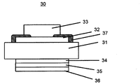
- FIG. 3 is a cross-sectional view schematically showing the Schottky barrier diode element obtained in Example 11.
- an IGO film 32 of an oxide semiconductor was sputtered on an n-type silicon substrate 31 and annealed in air at 300 ° C. for 1 hour, and then a negative resist manufactured by AZ Materials was spin-coated. Was applied.
- a pattern dug in a ring shape was formed at the edge (end portion) of the IGO film by pre-baking, exposure, development, and post-baking.
- Example 12 An n-type silicon (Si) substrate having a resistivity of 0.02 ⁇ ⁇ cm was prepared and treated with dilute hydrofluoric acid to remove the natural oxide film formed on the surface of the substrate. This Si substrate was mounted on a sputtering apparatus (manufactured by Shimadzu Corporation: HSM552), and Ti was first formed as an ohmic electrode.
- Si n-type silicon
- this IGO film was annealed in air at 300 ° C. for 1 hour, patterned by photolithography to form a desired pattern, and then annealed in air at 300 ° C. for 1 hour.
- the substrate with the amorphous IGO film was mounted on the sputtering apparatus again, and sputtering film formation was performed using a Ni target, and a Ni electrode was formed on the amorphous IGO film to obtain a Schottky junction. Further, Au was sputtered on the Ni electrode to obtain a Schottky barrier diode element having a simple configuration.
- the device obtained in the same manner as in Example 1 was evaluated. The results are shown in Table 2.
- Examples 13-20 A Schottky barrier diode element was fabricated and evaluated in the same manner as in Example 1 while appropriately changing the composition of the oxide semiconductor. The results are shown in Table 2. “4H—SiC” means a hexagonal SiC substrate having a four-layer repeating structure, and “YSZ” means an yttria-stabilized zirconia substrate. In Examples 13, 16, 18, 19, and 20, since a high-resistance substrate was used, electrical measurement was performed by placing terminals on the ohmic electrode and the Schottky electrode.
- Comparative Example 1 An n-type silicon (Si) substrate having a resistivity of 0.02 ⁇ ⁇ cm was prepared and treated with dilute hydrofluoric acid to remove the natural oxide film formed on the surface of the substrate. This Si substrate was mounted on a sputtering apparatus (manufactured by Shimadzu Corporation: HSM552), and Ti was first formed as an ohmic electrode. Next, a SiC target (manufactured by Sumitomo Osaka Cement Co., Ltd.) was used as a sputtering target, and sputter discharge was performed under the condition of RF 100 W to form a SiC film having a thickness of 1 ⁇ m on the Ti layer on the Ti-attached Si substrate.
- a SiC target manufactured by Sumitomo Osaka Cement Co., Ltd.
- this SiC film was patterned by photolithography to form a desired pattern, and then annealed in air at 300 ° C. for 1 hour. As a result of confirming the SiC film by XRD and SEM, it was polycrystalline.
- This substrate with polycrystalline SiC was again mounted on the sputtering apparatus, and sputtering film formation was performed using a Ni target, and a Ni electrode was formed on the polycrystalline SiC to obtain a Schottky junction. Further, Au was sputtered on the Ni electrode to obtain a Schottky barrier diode element having a simple configuration.
- the obtained device was evaluated in the same manner as in Example 1. The results are shown in Table 2.
- the device obtained in Comparative Example 1 showed a carrier concentration of 5 ⁇ 10 15 cm ⁇ 3 , but the n value exceeded 10 and did not show satisfactory diode characteristics. Also, the dielectric breakdown electric field remained at 0.1 MV / cm.
- Comparative Example 2 A Schottky barrier diode made of polycrystalline GaN was fabricated and evaluated in the same manner as in Comparative Example 1 except that single crystal GaN was used as the target instead of the SiC target. The results are shown in Table 2. The element obtained in Comparative Example 2 had an n value of more than 10 and did not exhibit satisfactory diode characteristics, and the dielectric breakdown electric field remained at 0.1 MV / cm.
- a Schottky barrier diode was fabricated and evaluated in the same manner as described above. The results are shown in Table 2.
- the device obtained in Comparative Example 3 had a very wide band gap of 5.8 eV or more, but the carrier concentration was very low, less than 10 13 cm ⁇ 3 , and a sufficient forward current could not be obtained.
- the Schottky barrier diode element of the present invention can be suitably used for an electric circuit, an electric device, an electronic device, an electric vehicle and the like that require high speed operation and switching characteristics.
Landscapes
- Electrodes Of Semiconductors (AREA)
- Chemical & Material Sciences (AREA)
- Crystallography & Structural Chemistry (AREA)
Priority Applications (6)
| Application Number | Priority Date | Filing Date | Title |
|---|---|---|---|
| CN202010532733.5A CN111668315B (zh) | 2013-08-19 | 2014-08-08 | 氧化物半导体基板及肖特基势垒二极管元件 |
| US14/912,815 US9691910B2 (en) | 2013-08-19 | 2014-08-08 | Oxide semiconductor substrate and schottky barrier diode |
| CN201480045490.5A CN105453272B (zh) | 2013-08-19 | 2014-08-08 | 氧化物半导体基板及肖特基势垒二极管元件 |
| JP2015532701A JPWO2015025499A1 (ja) | 2013-08-19 | 2014-08-08 | 酸化物半導体基板及びショットキーバリアダイオード |
| KR1020167004121A KR102226985B1 (ko) | 2013-08-19 | 2014-08-08 | 산화물 반도체 기판 및 쇼트키 배리어 다이오드 |
| US15/605,779 US11769840B2 (en) | 2013-08-19 | 2017-05-25 | Oxide semiconductor substrate and schottky barrier diode |
Applications Claiming Priority (2)
| Application Number | Priority Date | Filing Date | Title |
|---|---|---|---|
| JP2013169966 | 2013-08-19 | ||
| JP2013-169966 | 2013-08-19 |
Related Child Applications (2)
| Application Number | Title | Priority Date | Filing Date |
|---|---|---|---|
| US14/912,815 A-371-Of-International US9691910B2 (en) | 2013-08-19 | 2014-08-08 | Oxide semiconductor substrate and schottky barrier diode |
| US15/605,779 Continuation US11769840B2 (en) | 2013-08-19 | 2017-05-25 | Oxide semiconductor substrate and schottky barrier diode |
Publications (1)
| Publication Number | Publication Date |
|---|---|
| WO2015025499A1 true WO2015025499A1 (ja) | 2015-02-26 |
Family
ID=52483294
Family Applications (1)
| Application Number | Title | Priority Date | Filing Date |
|---|---|---|---|
| PCT/JP2014/004153 Ceased WO2015025499A1 (ja) | 2013-08-19 | 2014-08-08 | 酸化物半導体基板及びショットキーバリアダイオード |
Country Status (6)
| Country | Link |
|---|---|
| US (2) | US9691910B2 (enExample) |
| JP (3) | JPWO2015025499A1 (enExample) |
| KR (1) | KR102226985B1 (enExample) |
| CN (2) | CN105453272B (enExample) |
| TW (1) | TWI615984B (enExample) |
| WO (1) | WO2015025499A1 (enExample) |
Cited By (6)
| Publication number | Priority date | Publication date | Assignee | Title |
|---|---|---|---|---|
| WO2017111173A1 (ja) * | 2015-12-25 | 2017-06-29 | 出光興産株式会社 | 積層体 |
| WO2017111174A1 (ja) * | 2015-12-25 | 2017-06-29 | 出光興産株式会社 | 積層体 |
| JP2017120878A (ja) * | 2015-12-25 | 2017-07-06 | 出光興産株式会社 | 半導体素子及びそれを用いた電気機器 |
| JP2017201659A (ja) * | 2016-05-02 | 2017-11-09 | ローム株式会社 | 電子部品およびその製造方法 |
| KR20190057318A (ko) | 2016-10-11 | 2019-05-28 | 이데미쓰 고산 가부시키가이샤 | 구조물, 그 제조 방법, 반도체 소자 및 전자 회로 |
| CN110870079A (zh) * | 2017-07-08 | 2020-03-06 | 株式会社Flosfia | 半导体装置 |
Families Citing this family (9)
| Publication number | Priority date | Publication date | Assignee | Title |
|---|---|---|---|---|
| WO2017110940A1 (ja) * | 2015-12-25 | 2017-06-29 | 出光興産株式会社 | 半導体素子及びそれを用いた電気機器 |
| CN107039439B (zh) | 2016-02-04 | 2020-03-10 | 中芯国际集成电路制造(上海)有限公司 | 存储器及其形成方法 |
| US20180097073A1 (en) * | 2016-10-03 | 2018-04-05 | Flosfia Inc. | Semiconductor device and semiconductor system including semiconductor device |
| JP2018137394A (ja) * | 2017-02-23 | 2018-08-30 | トヨタ自動車株式会社 | 半導体装置の製造方法 |
| JP6977465B2 (ja) * | 2017-10-06 | 2021-12-08 | 株式会社デンソー | 半導体装置の製造方法 |
| GB2569196B (en) | 2017-12-11 | 2022-04-20 | Pragmatic Printing Ltd | Schottky diode |
| US11917919B2 (en) * | 2019-12-13 | 2024-02-27 | Denso Corporation | Electret |
| JP7638125B2 (ja) | 2021-03-25 | 2025-03-03 | エヌ・ティ・ティ・コミュニケーションズ株式会社 | 医療システム及びコンピュータープログラム |
| CN117954504A (zh) * | 2022-10-19 | 2024-04-30 | 广州华瑞升阳投资有限公司 | 一种肖特基势垒二极管 |
Citations (4)
| Publication number | Priority date | Publication date | Assignee | Title |
|---|---|---|---|---|
| JP2008021689A (ja) * | 2006-07-11 | 2008-01-31 | Fuji Electric Device Technology Co Ltd | 半導体装置 |
| WO2008096768A1 (ja) * | 2007-02-09 | 2008-08-14 | Idemitsu Kosan Co., Ltd. | 薄膜トランジスタの製造方法、薄膜トランジスタ、薄膜トランジスタ基板及び画像表示装置と、画像表示装置と、半導体デバイス |
| JP2009194225A (ja) * | 2008-02-15 | 2009-08-27 | Sumitomo Electric Ind Ltd | ショットキバリアダイオード、及びショットキバリアダイオードを作製する方法 |
| JP2012138552A (ja) * | 2010-12-28 | 2012-07-19 | Taiyo Yuden Co Ltd | ショットキーダイオードおよびその製造方法 |
Family Cites Families (64)
| Publication number | Priority date | Publication date | Assignee | Title |
|---|---|---|---|---|
| US4358782A (en) * | 1980-01-17 | 1982-11-09 | Asahi Kasei Kogyo Kabushiki Kaisha | Semiconductor device |
| US4782302A (en) * | 1986-10-31 | 1988-11-01 | The United States Of America As Represented By The United States Department Of Energy | Detector and energy analyzer for energetic-hydrogen in beams and plasmas |
| JP2702279B2 (ja) * | 1990-11-30 | 1998-01-21 | 新コスモス電機株式会社 | ガス検知素子 |
| JPH0536975A (ja) | 1991-03-07 | 1993-02-12 | Sumitomo Metal Ind Ltd | シヨツトキーバリアダイオード素子 |
| JPH04302173A (ja) * | 1991-03-29 | 1992-10-26 | Japan Synthetic Rubber Co Ltd | 薄膜ダイオード |
| JPH0897441A (ja) | 1994-09-26 | 1996-04-12 | Fuji Electric Co Ltd | 炭化けい素ショットキーダイオードの製造方法 |
| US20020179957A1 (en) * | 2001-05-29 | 2002-12-05 | Motorola, Inc. | Structure and method for fabricating high Q varactor diodes |
| JP2004022878A (ja) | 2002-06-18 | 2004-01-22 | Matsushita Electric Ind Co Ltd | 半導体装置およびその製造方法 |
| JP2005072367A (ja) * | 2003-08-26 | 2005-03-17 | Nippon Oil Corp | 光電変換素子 |
| JP5053537B2 (ja) * | 2004-11-10 | 2012-10-17 | キヤノン株式会社 | 非晶質酸化物を利用した半導体デバイス |
| US7863611B2 (en) | 2004-11-10 | 2011-01-04 | Canon Kabushiki Kaisha | Integrated circuits utilizing amorphous oxides |
| EP2453480A2 (en) * | 2004-11-10 | 2012-05-16 | Canon Kabushiki Kaisha | Amorphous oxide and field effect transistor |
| US20090090914A1 (en) * | 2005-11-18 | 2009-04-09 | Koki Yano | Semiconductor thin film, method for producing the same, and thin film transistor |
| KR100723420B1 (ko) * | 2006-02-20 | 2007-05-30 | 삼성전자주식회사 | 비정질 합금 산화층을 포함하는 비휘발성 메모리 소자 |
| JP2007243080A (ja) * | 2006-03-13 | 2007-09-20 | Fuji Electric Holdings Co Ltd | 半導体装置およびその製造方法 |
| US7389675B1 (en) * | 2006-05-12 | 2008-06-24 | The United States Of America As Represented By The National Aeronautics And Space Administration | Miniaturized metal (metal alloy)/ PdOx/SiC hydrogen and hydrocarbon gas sensors |
| JP5164357B2 (ja) * | 2006-09-27 | 2013-03-21 | キヤノン株式会社 | 半導体装置及び半導体装置の製造方法 |
| JP5261923B2 (ja) * | 2006-10-17 | 2013-08-14 | サンケン電気株式会社 | 化合物半導体素子 |
| JP4362635B2 (ja) * | 2007-02-02 | 2009-11-11 | ローム株式会社 | ZnO系半導体素子 |
| WO2008136505A1 (ja) | 2007-05-08 | 2008-11-13 | Idemitsu Kosan Co., Ltd. | 半導体デバイス及び薄膜トランジスタ、並びに、それらの製造方法 |
| JPWO2009034953A1 (ja) * | 2007-09-10 | 2010-12-24 | 出光興産株式会社 | 薄膜トランジスタ |
| JP2009164237A (ja) | 2007-12-28 | 2009-07-23 | Panasonic Corp | ショットキーバリアダイオード |
| US8076699B2 (en) * | 2008-04-02 | 2011-12-13 | The Hong Kong Univ. Of Science And Technology | Integrated HEMT and lateral field-effect rectifier combinations, methods, and systems |
| JP5382763B2 (ja) | 2008-04-09 | 2014-01-08 | 独立行政法人産業技術総合研究所 | 半導体素子及びその製造方法と、該半導体素子を備えた電子デバイス |
| JP5198146B2 (ja) * | 2008-05-22 | 2013-05-15 | 株式会社東芝 | 不揮発性記憶装置 |
| JP2010040552A (ja) * | 2008-07-31 | 2010-02-18 | Idemitsu Kosan Co Ltd | 薄膜トランジスタ及びその製造方法 |
| JP4803241B2 (ja) * | 2008-11-27 | 2011-10-26 | 三菱電機株式会社 | 半導体モジュール |
| JP5606682B2 (ja) * | 2009-01-29 | 2014-10-15 | 富士フイルム株式会社 | 薄膜トランジスタ、多結晶酸化物半導体薄膜の製造方法、及び薄膜トランジスタの製造方法 |
| JP2010182852A (ja) * | 2009-02-05 | 2010-08-19 | Konica Minolta Holdings Inc | 金属酸化物半導体、その製造方法及び薄膜トランジスタ |
| US8461582B2 (en) * | 2009-03-05 | 2013-06-11 | Semiconductor Energy Laboratory Co., Ltd. | Semiconductor device and method for manufacturing the same |
| US20100224878A1 (en) * | 2009-03-05 | 2010-09-09 | Semiconductor Energy Laboratory Co., Ltd. | Semiconductor device |
| JP5453867B2 (ja) * | 2009-03-24 | 2014-03-26 | 株式会社デンソー | ショットキーバリアダイオードを備えた炭化珪素半導体装置およびその製造方法 |
| JP5615018B2 (ja) * | 2009-04-10 | 2014-10-29 | 株式会社半導体エネルギー研究所 | 半導体装置および半導体装置の作製方法 |
| WO2010147073A1 (ja) | 2009-06-15 | 2010-12-23 | 株式会社村田製作所 | 抵抗スイッチング・メモリー素子 |
| JP2011029238A (ja) * | 2009-07-21 | 2011-02-10 | Fujifilm Corp | 結晶性ホモロガス化合物層を含む積層体の製造方法及び電界効果型トランジスタ |
| WO2011052437A1 (en) * | 2009-10-30 | 2011-05-05 | Semiconductor Energy Laboratory Co., Ltd. | Non-linear element, display device including non-linear element, and electronic device including display device |
| WO2011065210A1 (en) | 2009-11-28 | 2011-06-03 | Semiconductor Energy Laboratory Co., Ltd. | Stacked oxide material, semiconductor device, and method for manufacturing the semiconductor device |
| CN104992962B (zh) * | 2009-12-04 | 2018-12-25 | 株式会社半导体能源研究所 | 半导体器件及其制造方法 |
| WO2011099336A1 (en) * | 2010-02-12 | 2011-08-18 | Semiconductor Energy Laboratory Co., Ltd. | Semiconductor device and driving method thereof |
| KR101636998B1 (ko) * | 2010-02-12 | 2016-07-08 | 삼성디스플레이 주식회사 | 박막 트랜지스터 및 그 제조 방법 |
| US8835917B2 (en) | 2010-09-13 | 2014-09-16 | Semiconductor Energy Laboratory Co., Ltd. | Semiconductor device, power diode, and rectifier |
| JP5780902B2 (ja) * | 2010-10-12 | 2015-09-16 | 出光興産株式会社 | 半導体薄膜、薄膜トランジスタ及びその製造方法 |
| US20130320326A1 (en) * | 2011-02-18 | 2013-12-05 | Idemitsu Kosan Co., Ltd. | Insulating material forming composition for electronic devices, insulating material for electronic devices, electronic devices and thin film transistor |
| JP5800291B2 (ja) * | 2011-04-13 | 2015-10-28 | ローム株式会社 | ZnO系半導体素子およびその製造方法 |
| US8546879B2 (en) | 2011-08-18 | 2013-10-01 | Monolithic Power Systems, Inc. | High density lateral DMOS with recessed source contact |
| JP5894393B2 (ja) * | 2011-08-19 | 2016-03-30 | 出光興産株式会社 | 酸化物粒子分散液 |
| JP5866727B2 (ja) * | 2011-09-08 | 2016-02-17 | 株式会社タムラ製作所 | β−Ga2O3単結晶膜の製造方法及び結晶積層構造体 |
| US8902082B2 (en) | 2011-10-11 | 2014-12-02 | Bruce B. Roesner | Communicating statuses of vehicles |
| CN102332474A (zh) * | 2011-10-18 | 2012-01-25 | 北京工业大学 | 一种铟镓锌氧化物肖特基二极管器件及其制备方法 |
| JP2013102081A (ja) * | 2011-11-09 | 2013-05-23 | Tamura Seisakusho Co Ltd | ショットキーバリアダイオード |
| JP5984505B2 (ja) * | 2012-05-22 | 2016-09-06 | 株式会社日立製作所 | 半導体ガスセンサおよびその製造方法 |
| CN103426910B (zh) * | 2012-05-24 | 2016-01-20 | 杰力科技股份有限公司 | 功率半导体元件及其边缘终端结构 |
| US8952470B2 (en) * | 2012-09-10 | 2015-02-10 | James John Lupino | Low cost high density nonvolatile memory array device employing thin film transistors and back to back Schottky diodes |
| JP5777586B2 (ja) * | 2012-09-20 | 2015-09-09 | 株式会社東芝 | 半導体装置及びその製造方法 |
| JP6071569B2 (ja) * | 2013-01-17 | 2017-02-01 | キヤノン株式会社 | 有機発光素子 |
| JP6222931B2 (ja) * | 2013-01-21 | 2017-11-01 | キヤノン株式会社 | 有機発光素子 |
| JP6581765B2 (ja) * | 2013-10-02 | 2019-09-25 | 株式会社半導体エネルギー研究所 | ブートストラップ回路、およびブートストラップ回路を有する半導体装置 |
| US9300292B2 (en) * | 2014-01-10 | 2016-03-29 | Semiconductor Energy Laboratory Co., Ltd. | Circuit including transistor |
| JP6541360B2 (ja) * | 2014-02-07 | 2019-07-10 | 株式会社半導体エネルギー研究所 | 半導体装置 |
| US9842842B2 (en) * | 2014-03-19 | 2017-12-12 | Semiconductor Energy Laboratory Co., Ltd. | Semiconductor memory device and semiconductor device and electronic device having the same |
| JP6587497B2 (ja) * | 2014-10-31 | 2019-10-09 | 株式会社半導体エネルギー研究所 | 半導体装置 |
| TWI662792B (zh) * | 2015-01-29 | 2019-06-11 | 日商半導體能源研究所股份有限公司 | 半導體裝置、電子組件及電子裝置 |
| WO2016128853A1 (en) * | 2015-02-09 | 2016-08-18 | Semiconductor Energy Laboratory Co., Ltd. | Semiconductor device, electronic component, and electronic device |
| US9489988B2 (en) * | 2015-02-20 | 2016-11-08 | Semiconductor Energy Laboratory Co., Ltd. | Memory device |
-
2014
- 2014-08-08 JP JP2015532701A patent/JPWO2015025499A1/ja active Pending
- 2014-08-08 US US14/912,815 patent/US9691910B2/en active Active
- 2014-08-08 CN CN201480045490.5A patent/CN105453272B/zh active Active
- 2014-08-08 CN CN202010532733.5A patent/CN111668315B/zh active Active
- 2014-08-08 KR KR1020167004121A patent/KR102226985B1/ko active Active
- 2014-08-08 WO PCT/JP2014/004153 patent/WO2015025499A1/ja not_active Ceased
- 2014-08-15 TW TW103128165A patent/TWI615984B/zh active
-
2017
- 2017-05-25 US US15/605,779 patent/US11769840B2/en active Active
-
2019
- 2019-02-22 JP JP2019031008A patent/JP6989545B2/ja active Active
-
2020
- 2020-12-15 JP JP2020207470A patent/JP7084465B2/ja active Active
Patent Citations (4)
| Publication number | Priority date | Publication date | Assignee | Title |
|---|---|---|---|---|
| JP2008021689A (ja) * | 2006-07-11 | 2008-01-31 | Fuji Electric Device Technology Co Ltd | 半導体装置 |
| WO2008096768A1 (ja) * | 2007-02-09 | 2008-08-14 | Idemitsu Kosan Co., Ltd. | 薄膜トランジスタの製造方法、薄膜トランジスタ、薄膜トランジスタ基板及び画像表示装置と、画像表示装置と、半導体デバイス |
| JP2009194225A (ja) * | 2008-02-15 | 2009-08-27 | Sumitomo Electric Ind Ltd | ショットキバリアダイオード、及びショットキバリアダイオードを作製する方法 |
| JP2012138552A (ja) * | 2010-12-28 | 2012-07-19 | Taiyo Yuden Co Ltd | ショットキーダイオードおよびその製造方法 |
Cited By (18)
| Publication number | Priority date | Publication date | Assignee | Title |
|---|---|---|---|---|
| JP2021010031A (ja) * | 2015-12-25 | 2021-01-28 | 出光興産株式会社 | 半導体素子及びそれを用いた電気機器 |
| US10374045B2 (en) | 2015-12-25 | 2019-08-06 | Idemitsu Kosan Co., Ltd. | Semiconductor device and electric apparatus using same |
| JP2017120878A (ja) * | 2015-12-25 | 2017-07-06 | 出光興産株式会社 | 半導体素子及びそれを用いた電気機器 |
| TWI795349B (zh) * | 2015-12-25 | 2023-03-11 | 日商出光興產股份有限公司 | 積層體 |
| KR20180097546A (ko) | 2015-12-25 | 2018-08-31 | 이데미쓰 고산 가부시키가이샤 | 반도체 소자 및 그것을 사용한 전기 기기 |
| CN108475702A (zh) * | 2015-12-25 | 2018-08-31 | 出光兴产株式会社 | 层叠体 |
| JPWO2017111174A1 (ja) * | 2015-12-25 | 2018-10-18 | 出光興産株式会社 | 積層体 |
| JPWO2017111173A1 (ja) * | 2015-12-25 | 2018-10-18 | 出光興産株式会社 | 積層体 |
| WO2017111174A1 (ja) * | 2015-12-25 | 2017-06-29 | 出光興産株式会社 | 積層体 |
| US11189737B2 (en) | 2015-12-25 | 2021-11-30 | Idemitsu Kosan Co., Ltd. | Laminated body |
| US10340356B2 (en) | 2015-12-25 | 2019-07-02 | Idemitsu Kosan Co., Ltd. | Laminated article |
| CN108475702B (zh) * | 2015-12-25 | 2021-11-23 | 出光兴产株式会社 | 层叠体 |
| WO2017111173A1 (ja) * | 2015-12-25 | 2017-06-29 | 出光興産株式会社 | 積層体 |
| JP2017201659A (ja) * | 2016-05-02 | 2017-11-09 | ローム株式会社 | 電子部品およびその製造方法 |
| US11018238B2 (en) | 2016-10-11 | 2021-05-25 | Idemitsu Kosan Co., Ltd. | Structure, method for manufacturing same, semiconductor element, and electronic circuit |
| KR20190057318A (ko) | 2016-10-11 | 2019-05-28 | 이데미쓰 고산 가부시키가이샤 | 구조물, 그 제조 방법, 반도체 소자 및 전자 회로 |
| CN110870079A (zh) * | 2017-07-08 | 2020-03-06 | 株式会社Flosfia | 半导体装置 |
| CN110870079B (zh) * | 2017-07-08 | 2024-01-09 | 株式会社Flosfia | 半导体装置 |
Also Published As
| Publication number | Publication date |
|---|---|
| US9691910B2 (en) | 2017-06-27 |
| CN105453272B (zh) | 2020-08-21 |
| CN105453272A (zh) | 2016-03-30 |
| JP6989545B2 (ja) | 2022-01-05 |
| TW201515242A (zh) | 2015-04-16 |
| US11769840B2 (en) | 2023-09-26 |
| KR102226985B1 (ko) | 2021-03-11 |
| US20160197202A1 (en) | 2016-07-07 |
| TWI615984B (zh) | 2018-02-21 |
| JPWO2015025499A1 (ja) | 2017-03-02 |
| JP2019080084A (ja) | 2019-05-23 |
| JP2021052203A (ja) | 2021-04-01 |
| KR20160043967A (ko) | 2016-04-22 |
| CN111668315B (zh) | 2023-09-12 |
| US20170263786A1 (en) | 2017-09-14 |
| CN111668315A (zh) | 2020-09-15 |
| JP7084465B2 (ja) | 2022-06-14 |
Similar Documents
| Publication | Publication Date | Title |
|---|---|---|
| JP7084465B2 (ja) | 酸化物半導体基板及びショットキーバリアダイオード | |
| JP6283364B2 (ja) | 酸化物半導体基板及びショットキーバリアダイオード | |
| TWI731844B (zh) | 積層體 | |
| KR101824124B1 (ko) | 반도체 장치 및 그 제작 방법 | |
| CN108369964A (zh) | 层叠体 | |
| KR20180099655A (ko) | 적층체 | |
| WO2016132681A1 (ja) | 積層体及び積層体の製造方法 |
Legal Events
| Date | Code | Title | Description |
|---|---|---|---|
| WWE | Wipo information: entry into national phase |
Ref document number: 201480045490.5 Country of ref document: CN |
|
| 121 | Ep: the epo has been informed by wipo that ep was designated in this application |
Ref document number: 14837818 Country of ref document: EP Kind code of ref document: A1 |
|
| ENP | Entry into the national phase |
Ref document number: 2015532701 Country of ref document: JP Kind code of ref document: A |
|
| ENP | Entry into the national phase |
Ref document number: 20167004121 Country of ref document: KR Kind code of ref document: A |
|
| WWE | Wipo information: entry into national phase |
Ref document number: 14912815 Country of ref document: US |
|
| NENP | Non-entry into the national phase |
Ref country code: DE |
|
| 122 | Ep: pct application non-entry in european phase |
Ref document number: 14837818 Country of ref document: EP Kind code of ref document: A1 |