US8076699B2 - Integrated HEMT and lateral field-effect rectifier combinations, methods, and systems - Google Patents
Integrated HEMT and lateral field-effect rectifier combinations, methods, and systems Download PDFInfo
- Publication number
- US8076699B2 US8076699B2 US12/414,865 US41486509A US8076699B2 US 8076699 B2 US8076699 B2 US 8076699B2 US 41486509 A US41486509 A US 41486509A US 8076699 B2 US8076699 B2 US 8076699B2
- Authority
- US
- United States
- Prior art keywords
- nitride
- diode
- layer
- schottky
- gan
- Prior art date
- Legal status (The legal status is an assumption and is not a legal conclusion. Google has not performed a legal analysis and makes no representation as to the accuracy of the status listed.)
- Active, expires
Links
- 230000005669 field effect Effects 0.000 title claims abstract description 35
- 238000000034 method Methods 0.000 title abstract description 29
- 239000004065 semiconductor Substances 0.000 claims abstract description 34
- 229910002601 GaN Inorganic materials 0.000 claims description 50
- 230000004888 barrier function Effects 0.000 claims description 29
- 229910052731 fluorine Inorganic materials 0.000 claims description 17
- 239000011737 fluorine Substances 0.000 claims description 17
- -1 fluorine ions Chemical class 0.000 claims description 6
- JMASRVWKEDWRBT-UHFFFAOYSA-N Gallium nitride Chemical compound [Ga]#N JMASRVWKEDWRBT-UHFFFAOYSA-N 0.000 claims description 5
- 230000006911 nucleation Effects 0.000 claims 1
- 238000010899 nucleation Methods 0.000 claims 1
- 238000004519 manufacturing process Methods 0.000 abstract description 14
- KRHYYFGTRYWZRS-UHFFFAOYSA-M Fluoride anion Chemical compound [F-] KRHYYFGTRYWZRS-UHFFFAOYSA-M 0.000 abstract description 9
- 239000000463 material Substances 0.000 abstract description 7
- 229910002704 AlGaN Inorganic materials 0.000 description 41
- 230000008569 process Effects 0.000 description 14
- YCKRFDGAMUMZLT-UHFFFAOYSA-N Fluorine atom Chemical compound [F] YCKRFDGAMUMZLT-UHFFFAOYSA-N 0.000 description 11
- 230000015556 catabolic process Effects 0.000 description 10
- 230000002441 reversible effect Effects 0.000 description 10
- 238000002513 implantation Methods 0.000 description 9
- 238000005468 ion implantation Methods 0.000 description 9
- 238000010586 diagram Methods 0.000 description 7
- 229910052751 metal Inorganic materials 0.000 description 7
- 239000002184 metal Substances 0.000 description 7
- 230000008901 benefit Effects 0.000 description 6
- 230000010354 integration Effects 0.000 description 6
- 239000000523 sample Substances 0.000 description 6
- 238000006243 chemical reaction Methods 0.000 description 5
- 238000013461 design Methods 0.000 description 5
- 238000001465 metallisation Methods 0.000 description 4
- 238000009832 plasma treatment Methods 0.000 description 4
- 238000004151 rapid thermal annealing Methods 0.000 description 4
- 235000012431 wafers Nutrition 0.000 description 4
- 229910004205 SiNX Inorganic materials 0.000 description 3
- 230000000903 blocking effect Effects 0.000 description 3
- 150000002500 ions Chemical class 0.000 description 3
- 238000002955 isolation Methods 0.000 description 3
- 239000000203 mixture Substances 0.000 description 3
- 238000002161 passivation Methods 0.000 description 3
- 238000000623 plasma-assisted chemical vapour deposition Methods 0.000 description 3
- 239000000758 substrate Substances 0.000 description 3
- 239000000956 alloy Substances 0.000 description 2
- 229910045601 alloy Inorganic materials 0.000 description 2
- 238000000137 annealing Methods 0.000 description 2
- 230000007423 decrease Effects 0.000 description 2
- 230000007547 defect Effects 0.000 description 2
- 238000000151 deposition Methods 0.000 description 2
- 230000008021 deposition Effects 0.000 description 2
- 238000001312 dry etching Methods 0.000 description 2
- 230000008020 evaporation Effects 0.000 description 2
- 238000001704 evaporation Methods 0.000 description 2
- 238000009616 inductively coupled plasma Methods 0.000 description 2
- 238000012986 modification Methods 0.000 description 2
- 230000004048 modification Effects 0.000 description 2
- 229910003465 moissanite Inorganic materials 0.000 description 2
- 230000005693 optoelectronics Effects 0.000 description 2
- 238000001020 plasma etching Methods 0.000 description 2
- 230000004044 response Effects 0.000 description 2
- 229910052594 sapphire Inorganic materials 0.000 description 2
- 239000010980 sapphire Substances 0.000 description 2
- 229910010271 silicon carbide Inorganic materials 0.000 description 2
- 230000001360 synchronised effect Effects 0.000 description 2
- 238000012546 transfer Methods 0.000 description 2
- 230000001052 transient effect Effects 0.000 description 2
- 101100269850 Caenorhabditis elegans mask-1 gene Proteins 0.000 description 1
- XUIMIQQOPSSXEZ-UHFFFAOYSA-N Silicon Chemical compound [Si] XUIMIQQOPSSXEZ-UHFFFAOYSA-N 0.000 description 1
- 239000008186 active pharmaceutical agent Substances 0.000 description 1
- 238000005452 bending Methods 0.000 description 1
- 238000005229 chemical vapour deposition Methods 0.000 description 1
- 238000002485 combustion reaction Methods 0.000 description 1
- 230000000052 comparative effect Effects 0.000 description 1
- 150000001875 compounds Chemical class 0.000 description 1
- 238000010276 construction Methods 0.000 description 1
- 238000012937 correction Methods 0.000 description 1
- 230000000694 effects Effects 0.000 description 1
- 238000005516 engineering process Methods 0.000 description 1
- 238000000407 epitaxy Methods 0.000 description 1
- 210000003127 knee Anatomy 0.000 description 1
- 230000007246 mechanism Effects 0.000 description 1
- 150000002739 metals Chemical class 0.000 description 1
- 150000004767 nitrides Chemical class 0.000 description 1
- 239000003921 oil Substances 0.000 description 1
- 238000011017 operating method Methods 0.000 description 1
- 238000000059 patterning Methods 0.000 description 1
- RVZRBWKZFJCCIB-UHFFFAOYSA-N perfluorotributylamine Chemical compound FC(F)(F)C(F)(F)C(F)(F)C(F)(F)N(C(F)(F)C(F)(F)C(F)(F)C(F)(F)F)C(F)(F)C(F)(F)C(F)(F)C(F)(F)F RVZRBWKZFJCCIB-UHFFFAOYSA-N 0.000 description 1
- 230000002093 peripheral effect Effects 0.000 description 1
- 230000010287 polarization Effects 0.000 description 1
- 238000012545 processing Methods 0.000 description 1
- 239000000700 radioactive tracer Substances 0.000 description 1
- 238000011084 recovery Methods 0.000 description 1
- 230000008439 repair process Effects 0.000 description 1
- 238000011160 research Methods 0.000 description 1
- 239000004576 sand Substances 0.000 description 1
- 229910052710 silicon Inorganic materials 0.000 description 1
- 239000010703 silicon Substances 0.000 description 1
- 230000002269 spontaneous effect Effects 0.000 description 1
- 238000006467 substitution reaction Methods 0.000 description 1
- 230000005533 two-dimensional electron gas Effects 0.000 description 1
Images


Classifications
-
- H—ELECTRICITY
- H01—ELECTRIC ELEMENTS
- H01L—SEMICONDUCTOR DEVICES NOT COVERED BY CLASS H10
- H01L27/00—Devices consisting of a plurality of semiconductor or other solid-state components formed in or on a common substrate
- H01L27/02—Devices consisting of a plurality of semiconductor or other solid-state components formed in or on a common substrate including semiconductor components specially adapted for rectifying, oscillating, amplifying or switching and having at least one potential-jump barrier or surface barrier; including integrated passive circuit elements with at least one potential-jump barrier or surface barrier
- H01L27/04—Devices consisting of a plurality of semiconductor or other solid-state components formed in or on a common substrate including semiconductor components specially adapted for rectifying, oscillating, amplifying or switching and having at least one potential-jump barrier or surface barrier; including integrated passive circuit elements with at least one potential-jump barrier or surface barrier the substrate being a semiconductor body
- H01L27/06—Devices consisting of a plurality of semiconductor or other solid-state components formed in or on a common substrate including semiconductor components specially adapted for rectifying, oscillating, amplifying or switching and having at least one potential-jump barrier or surface barrier; including integrated passive circuit elements with at least one potential-jump barrier or surface barrier the substrate being a semiconductor body including a plurality of individual components in a non-repetitive configuration
- H01L27/0605—Devices consisting of a plurality of semiconductor or other solid-state components formed in or on a common substrate including semiconductor components specially adapted for rectifying, oscillating, amplifying or switching and having at least one potential-jump barrier or surface barrier; including integrated passive circuit elements with at least one potential-jump barrier or surface barrier the substrate being a semiconductor body including a plurality of individual components in a non-repetitive configuration integrated circuits made of compound material, e.g. AIIIBV
-
- H—ELECTRICITY
- H01—ELECTRIC ELEMENTS
- H01L—SEMICONDUCTOR DEVICES NOT COVERED BY CLASS H10
- H01L27/00—Devices consisting of a plurality of semiconductor or other solid-state components formed in or on a common substrate
- H01L27/02—Devices consisting of a plurality of semiconductor or other solid-state components formed in or on a common substrate including semiconductor components specially adapted for rectifying, oscillating, amplifying or switching and having at least one potential-jump barrier or surface barrier; including integrated passive circuit elements with at least one potential-jump barrier or surface barrier
- H01L27/04—Devices consisting of a plurality of semiconductor or other solid-state components formed in or on a common substrate including semiconductor components specially adapted for rectifying, oscillating, amplifying or switching and having at least one potential-jump barrier or surface barrier; including integrated passive circuit elements with at least one potential-jump barrier or surface barrier the substrate being a semiconductor body
- H01L27/06—Devices consisting of a plurality of semiconductor or other solid-state components formed in or on a common substrate including semiconductor components specially adapted for rectifying, oscillating, amplifying or switching and having at least one potential-jump barrier or surface barrier; including integrated passive circuit elements with at least one potential-jump barrier or surface barrier the substrate being a semiconductor body including a plurality of individual components in a non-repetitive configuration
- H01L27/0611—Devices consisting of a plurality of semiconductor or other solid-state components formed in or on a common substrate including semiconductor components specially adapted for rectifying, oscillating, amplifying or switching and having at least one potential-jump barrier or surface barrier; including integrated passive circuit elements with at least one potential-jump barrier or surface barrier the substrate being a semiconductor body including a plurality of individual components in a non-repetitive configuration integrated circuits having a two-dimensional layout of components without a common active region
- H01L27/0617—Devices consisting of a plurality of semiconductor or other solid-state components formed in or on a common substrate including semiconductor components specially adapted for rectifying, oscillating, amplifying or switching and having at least one potential-jump barrier or surface barrier; including integrated passive circuit elements with at least one potential-jump barrier or surface barrier the substrate being a semiconductor body including a plurality of individual components in a non-repetitive configuration integrated circuits having a two-dimensional layout of components without a common active region comprising components of the field-effect type
- H01L27/0629—Devices consisting of a plurality of semiconductor or other solid-state components formed in or on a common substrate including semiconductor components specially adapted for rectifying, oscillating, amplifying or switching and having at least one potential-jump barrier or surface barrier; including integrated passive circuit elements with at least one potential-jump barrier or surface barrier the substrate being a semiconductor body including a plurality of individual components in a non-repetitive configuration integrated circuits having a two-dimensional layout of components without a common active region comprising components of the field-effect type in combination with diodes, or resistors, or capacitors
-
- H—ELECTRICITY
- H01—ELECTRIC ELEMENTS
- H01L—SEMICONDUCTOR DEVICES NOT COVERED BY CLASS H10
- H01L29/00—Semiconductor devices adapted for rectifying, amplifying, oscillating or switching, or capacitors or resistors with at least one potential-jump barrier or surface barrier, e.g. PN junction depletion layer or carrier concentration layer; Details of semiconductor bodies or of electrodes thereof ; Multistep manufacturing processes therefor
- H01L29/66—Types of semiconductor device ; Multistep manufacturing processes therefor
- H01L29/68—Types of semiconductor device ; Multistep manufacturing processes therefor controllable by only the electric current supplied, or only the electric potential applied, to an electrode which does not carry the current to be rectified, amplified or switched
- H01L29/76—Unipolar devices, e.g. field effect transistors
- H01L29/772—Field effect transistors
- H01L29/778—Field effect transistors with two-dimensional charge carrier gas channel, e.g. HEMT ; with two-dimensional charge-carrier layer formed at a heterojunction interface
- H01L29/7786—Field effect transistors with two-dimensional charge carrier gas channel, e.g. HEMT ; with two-dimensional charge-carrier layer formed at a heterojunction interface with direct single heterostructure, i.e. with wide bandgap layer formed on top of active layer, e.g. direct single heterostructure MIS-like HEMT
- H01L29/7787—Field effect transistors with two-dimensional charge carrier gas channel, e.g. HEMT ; with two-dimensional charge-carrier layer formed at a heterojunction interface with direct single heterostructure, i.e. with wide bandgap layer formed on top of active layer, e.g. direct single heterostructure MIS-like HEMT with wide bandgap charge-carrier supplying layer, e.g. direct single heterostructure MODFET
-
- H—ELECTRICITY
- H01—ELECTRIC ELEMENTS
- H01L—SEMICONDUCTOR DEVICES NOT COVERED BY CLASS H10
- H01L29/00—Semiconductor devices adapted for rectifying, amplifying, oscillating or switching, or capacitors or resistors with at least one potential-jump barrier or surface barrier, e.g. PN junction depletion layer or carrier concentration layer; Details of semiconductor bodies or of electrodes thereof ; Multistep manufacturing processes therefor
- H01L29/66—Types of semiconductor device ; Multistep manufacturing processes therefor
- H01L29/86—Types of semiconductor device ; Multistep manufacturing processes therefor controllable only by variation of the electric current supplied, or only the electric potential applied, to one or more of the electrodes carrying the current to be rectified, amplified, oscillated or switched
- H01L29/861—Diodes
- H01L29/872—Schottky diodes
-
- H—ELECTRICITY
- H01—ELECTRIC ELEMENTS
- H01L—SEMICONDUCTOR DEVICES NOT COVERED BY CLASS H10
- H01L29/00—Semiconductor devices adapted for rectifying, amplifying, oscillating or switching, or capacitors or resistors with at least one potential-jump barrier or surface barrier, e.g. PN junction depletion layer or carrier concentration layer; Details of semiconductor bodies or of electrodes thereof ; Multistep manufacturing processes therefor
- H01L29/02—Semiconductor bodies ; Multistep manufacturing processes therefor
- H01L29/12—Semiconductor bodies ; Multistep manufacturing processes therefor characterised by the materials of which they are formed
- H01L29/20—Semiconductor bodies ; Multistep manufacturing processes therefor characterised by the materials of which they are formed including, apart from doping materials or other impurities, only AIIIBV compounds
- H01L29/2003—Nitride compounds
Definitions
- the present application relates to III-N-type power devices, methods, and systems, and more particularly to III-N-type integrated power devices having heterostructure transistors and lateral field-effect rectifiers on the same chip, and to related manufacturing methods, operating methods, and systems.
- Power semiconductor devices include two categories: 1) three-terminal transistors as switches and 2) two-terminal rectifiers. Both rectifiers and transistors are essential components in high voltage power electronics applications, for example, switching-mode power supplies and many forms of drive circuits.
- HEMTs high electron mobility transistors
- Group III-nitride (“III-N”) compound semiconductors such as those incorporating AlGaN/GaN, possess the advantages of having wide bandgap, high breakdown field, and large thermal conductivity, which can bring significant benefits to the design of heterostructure field-effect transistors and applications.
- the wide-bandgap AlGaN/GaN heterostructure system enhanced by the spontaneous and piezoelectric polarization effects, yields two-dimensional electron gas (2DEG) channel with a high sheet charge concentration and high electron mobility.
- 2DEG two-dimensional electron gas
- AlGaN/GaN heterostructures for power electronics application can operate at higher temperature and higher switching frequency than other device types.
- the GaN semiconductors may present an on-resistance (R on ) that is three orders of magnitude lower than Si semiconductors.
- V F,ON forward turn-on voltage
- R ON, sp specific on-resistance
- BV reverse breakdown voltage
- JBS junction barrier Schottky
- MPS merged p-i-n Schottky
- SBDs Schottky barrier diodes
- p-i-n diodes on doped bulk GaN which presents high-breakdown low-on-resistance features.
- the SBD or p-i-n diode rectifiers have not been successfully integrated with HEMTs (at least not without unacceptable performance loss).
- SBDs can be directly formed on AlGaN/GaN heterostructures, the series combination of the AlGaN/GaN heterojunction with the metal-AlGaN Schottky barrier results in higher turn-on voltages and higher on-resistances.
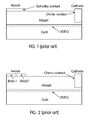
- a recently developed dual-metal SBD system ( FIG. 2 ) combines a low Schottky barrier metal (Al/Ti) and a high Schottky barrier metal (Pt) to provide an anode with a low turn-on voltage.
- Al/Ti low Schottky barrier metal
- Pt high Schottky barrier metal
- the present application discloses new structures and methods in which merged rectifiers (e.g. Schottky plus field-effect diodes) are integrated with HEMT-type transistors, in III-N semiconductor material or the like. This allows high performance rectifiers and transistors to be manufactured on the same chip in one process.
- merged rectifiers e.g. Schottky plus field-effect diodes
- III-N semiconductor material or the like III-N semiconductor material or the like.
- the various disclosed integrated structures will produce electronic devices capable of operation at high power levels, high temperatures, and in noisy environments. This is particularly advantageous e.g. for compact and/or high-efficiency power converters, for motor drive circuits, for audio amplifiers, for local interface to combustion engines, for various aerospace applications, and for downhole electronics in oil and gas wells.
- the integrated structure provides both a merged power rectifier, with low turn-on voltage, low on-resistance, high breakdown voltage and high switching speed, and also a normally-off AlGaN/GaN heterostructure transistor, in a combination which uses the same epitaxial wafers as well as the same fabricating process.
- the rectifier incorporates negatively charged fluorine ions under the Schottky contact by Fluorine plasma ion implantation (or treatment) technique, which effectively depletes the 2DEG under the Schottky contact region and pinches off the conduction path.
- Fluorine plasma ion implantation (or treatment) technique By electrically shorting the Schottky gate and anode ohmic contact together, the turn-on voltage is determined by the threshold voltage of the channel instead of the Schottky barrier or p-n barrier.
- a lateral field effect rectifier and a normally-off HEMT are manufactured on the same chip in one process and the HEMT is of the conventional Ni/Au gate metallization.
- an integrated field effect rectifier and a normally-off HEMT are manufactured self-aligned in one process.
- This integrated structure is particularly advantageous for power converter circuits.
- Lower R on means lower power consumption for power converter circuits, thus higher power conversion efficiency.
- This means that power converter modules which use the above technologies can be very compact and lightweight, with smaller heatsinks to control temperature. Because of the capability for higher switching frequencies the size of the reactive passive components can also be significantly reduced, with improved performance. High temperature tolerance allows such HEMTs to be used in high temperature and stringent environments.
- the structures described above are integrated with a light-emitting diode structure. These embodiments permit a variety of new applications, including, for example, power converters with integrated failure indication, or a complete multivoltage and/or mains-operated LED lighting module.
- the disclosed innovations in various embodiments, provide one or more of at least the following advantages. (However, not all of these advantages result from every one of the innovations disclosed, and this list of advantages does not limit the various claimed inventions.)
- FIG. 1 is the cross-section of a conventional AlGaN/GaN SBD structure.
- FIG. 2 is the cross-section of a dual-metal AlGaN/GaN SBD structure.
- FIG. 3 is the cross-section of an AlGaN/GaN HEMT-compatible power lateral field-effect rectifier structure in accordance with the present application.
- FIGS. 4( a )- 4 ( c ) show the comparative effects on the conduction-band diagrams and the electron concentrations with/without fluorine ion implantation in an AlGaN/GaN HEMT.
- FIGS. 5( a )- 5 ( e ) demonstrate an example manufacturing process for an AlGaN/GaN HEMT-compatible power lateral field-effect rectifier in accordance with the present application.
- FIGS. 6( a )- 6 ( d ) demonstrate an example of a manufacturing process for a normally-off AlGaN/GaN HEMT integrated with a lateral field-effect rectifier on the same chip in accordance with the present application.
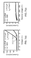
- FIGS. 7( a ) and 7 ( b ) show the forward and reverse characteristics of a lateral field-effect rectifier fabricated in accordance with the present application.
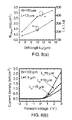
- FIG. 8( a ) shows the dependence of specific on-resistance and breakdown voltage on the drift length in the lateral field-effect rectifier fabricated in accordance with the present application.
- FIG. 8( b ) shows the forward bias current-voltage characteristics of lateral field-effect rectifiers with a drift length of 5 ⁇ m, 10 ⁇ m, and 15 ⁇ m fabricated in accordance with the present application.
- FIG. 9 shows the temperature dependence of the forward characteristics of a lateral field-effect rectifier fabricated in accordance with the present application.
- the currents are normalized against the current measured with 3 V forward bias at room temperature (RT).
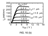
- FIGS. 10( a )- 10 ( b ) show the performance of a normally-off HEMT manufactured in accordance with the present application: (a) transfer characteristics and (b) source-drain output characteristics.
- FIG. 11( a ) shows an example of a single-chip GaN-based Boost converter containing an integrated AlGaN/GaN HEMT and power lateral field-effect rectifier chip in accordance with the present application.
- FIG. 11( b ) displays the measured waveforms of the Boost converter in FIG. 9( a ).
- FIG. 11( c ) shows an integrated buck converter which combines a HEMT switch and a rectifier.
- FIG. 12 shows an AC-DC converter featuring integration of rectifiers with a power HEMT switch.
- FIG. 13 shows a block diagram of an intelligent power switch.
- FIG. 14 shows an equivalent circuit diagram of a merged device structure.
- FIG. 15 shows of many of the different device types which can all be integrated together.
- FIGS. 16( a )- 16 ( c ) show three more integrated structures and methods, in which diodes and transistors are integrated with various light-emitting diode structures.
- FIG. 3 shows a schematic cross-section of the power lateral field-effect rectifier (L-FER) 301 integrated with a normally-off HEMT 303 .
- Dimension L is the length of the Schottky contact region (Fluorine ion implantation length), and dimension L D is the length of the drift region of the L-FER 301 .
- Dimension L GS is the gate-source distance, L G is the gate length, and L GD is the gate-drain distance of HEMT 303 .
- HEMT 303 includes a source 315 , a gate 317 , and a drain 319 on the surface of AlGaN layer 321 over GaN layer 325 .
- a 2DEG electron gas 323 forms.
- the voltage applied to the gate electrode will invert a portion of the semiconductor material to form an extension of this 2DEG which completes the circuit from source to drain.
- AlGaN layer 321 over GaN layer 325 are grown over a substrate layer 327 , that is usually made of Si, SiC, Sapphire or GaN.
- a region 329 containing permanently negatively charged ions generally fluorine ions (F ⁇ ) which have been introduced by CF 4 plasma treatment or by ion implantation. Region 329 may also extend into the GaN layer. Details of F— implantation are described in US patent publication US 2007/0278518 Al to the inventor of this application, Chen et al, which is hereby incorporated by reference in its entirety.
- L-FER 301 The structure of L-FER 301 is somewhat similar to that of an AlGaN/GaN normally-off HEMT structure.
- L-FER 301 also contains AlGaN layer 321 over GaN layer 325 . Between AlGaN layer 321 and GaN layer 325 , forms the 2DEG electron gas channel 323 .
- AlGaN layer 321 , and underlying GaN layer 325 are successively grown over a substrate layer 327 , typically of Si, SiC, Sapphire or GaN. On the surface of AlGaN layer 321 sits the cathode electrode 331 .
- Cathode 331 is made of an electrode in ohmic contact with the AlGaN layer (and hence with the underlying 2DEG), and the anode electrode 333 is made of electrically shorted Schottky contact 335 and ohmic contact 339 .
- Underneath the Schottky contact 335 is a region 337 containing permanently negatively charged ions.
- F ⁇ fluorine ions
- Region 337 may vertically extend into the GaN layer.
- lateral isolation between the rectifier and the transistor is provided, in this example, by mesa isolation.
- FIG. 4( a ) shows the simulated conduction-band diagrams for the structure of FIG. 3 without fluorine ion implantation at zero gate bias.
- FIG. 4( b ) shows the simulated conduction-band diagrams for the structure of FIG. 3 with fluorine ion implantation at zero gate bias.
- FIG. 4( b ) shows that the fluorine ion treatment causes the conduction-band bending upward, especially in AlGaN barrier, yielding an additional barrier height ⁇ F .
- the conduction-band minimum of the 2DEG channel of the fluorine-treated structure is above Fermi level, indicating a completely depleted channel. The enhanced barrier will significantly suppress the reverse leakage current of the Schottky contact region.
- FIG. 4( c ) shows the electron profiles of the fluorine treated and untreated structures. There are no electrons in the channel under the zero gate bias in the plasma-treated structure, indicating a normally-off device.
- FIGS. 5( a )- 5 ( e ) show an example of a fabrication process for the lateral field-effect rectifier structure shown in FIG. 3 .
- a device mesa 501 was formed on AlGaN/GaN surface 503 .
- this step was implemented using a Cl 2 /He plasma dry etching in an inductively coupled plasma reactive ion etching (ICP-RIE) system.
- ICP-RIE inductively coupled plasma reactive ion etching
- the Ohmic contacts 505 are formed.
- this step was implemented by a deposition of e-beam evaporated Ti/Al/Ni/Au (20 nm/150 nm/50 nm/80 nm) and rapid thermal annealing (RTA) at 850° C. for 30 s with Mask 2 .
- RTA rapid thermal annealing
- a fluorine ion implantation 507 is implemented next to Ohmic contact region 505 and self-aligned to define the electrode contact, with Mask 3 .
- the fluorine ion implantation is controlled in order to optimize the trade-off between the reverse blocking capability and the turn-on voltage.
- a passivation layer 509 (e.g. 300 nm thickness of SiN x ) is deposited, e.g. by the PECVD with Mask 5 .
- the probing pads 511 and field plate (FP) 513 are defined and formed with Mask 6 .
- the sample is preferably annealed, e.g. at 400° C. for 10 min, to repair the plasma-induced damage in the AlGaN barrier.
- FIGS. 6( a )- 6 ( d ) show an example of a similar manufacturing process for fabricating an integrated lateral field-effect rectifier and a normally-off HEMT on one chip.
- a device mesa was formed using a Cl 2 /He plasma dry etching in an inductively coupled plasma reactive ion etching (ICP-RIE) system. Multiple structure areas may be formed.
- the figures display two representative structure areas 601 and 603 .
- the ohmic contacts 605 are formed by a deposition of e-beam evaporated Ti/Al/Ni/Au (20 nm/150 nm/50 nm/80 nm) and rapid thermal annealing (RTA) at 850° C. for 30 s. This step forms contacts on both the rectifier and the HEMT.
- RTA rapid thermal annealing
- a fluorine-based plasma treatment is implemented, self-aligned to the Schottky electrode locations, using mask 606 .
- Fluorine implantation regions 609 and 613 are formed for the rectifier and the HEMT respectively.
- Fluorine implantation region 609 is self-aligned to the edge of the anode ohmic contact of the rectifier 601 , and fluorine implantation region 613 is more to the middle between the two contacts of the HEMT 603 .
- the Fluorine implantation is controlled in order to optimize the trade-off between the reverse blocking capability and the turn-on voltage.
- This implantation is followed, in this example, by the e-beam evaporation of Ni/Au Schottky contact 611 as shown in FIG. 6( d ).
- the Schottky contact 611 is deposited on the uncovered surface of the fluorine implantation region of the AlGaN surface, forming an electrically shorted Schottky contact and ohmic contact in rectifier 601 .
- the Schottky contact 611 is deposited on the uncovered surface of the fluorine implantation region forming the gate.
- a sample device structure of FIG. 3 is fabricated by using commercially available Al 0.26 Ga 0.74 N/GaN HEMT wafer grown by metal organic chemical vapor deposition (MOCVD) on silicon substrate.
- the epitaxial structure includes a GaN buffer, a thin AlN interface enhancement layer, a ⁇ 18 nm undoped AlGaN layer and a 2 nm undoped GaN cap.
- the starting wafer features a sheet resistance of 320 ohm/square, 2DEG mobility of 1800 cm 2 /V•s and a pinch off voltage of ⁇ 2.1 V.
- the specific contact resistance of ⁇ 1.0 ⁇ .mm is obtained using a standard transfer length method (TLM) procedure.
- TLM transfer length method
- the forward characteristics of the above fabricated L-FER and the SBD with the same anode-cathode drift region length (L D ) of 10 ⁇ m and the same device width (W) of 100 ⁇ m are plotted in FIG. 7( a ).
- the knee voltage (V k , defined as the anode bias at a forward current of 1 mA/mm) is 0.2 V in the L-FER and 1.3 V in the SBD. This large difference is a result of the different turn-on mechanisms in the two devices.
- V k is decided by the pinch-off voltage of the channel, and can be well adjusted and controlled by the fluorine plasma power and implantation time.
- V k is determined by the metal/AlGaN Schottky barrier as well as the conduction band offset at the AlGaN/GaN heterointerface.
- the specific on-resistance (R ON,sp ) is 1.4 m ⁇ .cm 2 in the L-FER, where R ON,sp is calculated in the forward bias range of 2 V to 3V using the area of the active region excluding the ohmic contacts.
- the reverse breakdown characteristics of the two devices were measured using Tektronix 370A curve tracer without immersing the devices in Fluorinert, and are plotted in FIG. 7( b ).
- the L-FER and SBD with the same drift region length of 10 ⁇ m exhibit nearly-identical reverse breakdown voltage at a current of 1 mA/mm.
- the BV for L-FER with a 10 ⁇ m drift length is 390 V, leading to a power figure of merit (BV 2 /R ON, sp ) of 108 MW ⁇ cm ⁇ 2 , comparable to that reported in the vertical Schottky diode.
- FIG. 8( a ) The dependences of R ON, sp and BV on the drift length (L D ) of the L-FER are plotted in FIG. 8( a ). Both BV and R ON, sp are increased as the drift length increases.
- the forward turn-on characteristics of L-FERs with different drift lengths are plotted in FIG. 8( b ).
- V F,ON is attributed to the turn-on control scheme by the channel threshold voltage instead of Schottky junction or p-i-n junction.
- the high 2DEG density and mobility in the drift region enables the achievement of low on-resistance, which also leads to the low V F,ON in L-FER.
- FIG. 9 shows the temperature dependences of the forward bias characteristics in the L-FERs using a probe station with thermal chuck.
- V k shows little temperature dependence as the temperature rises to 250° C., although the current decreases with the increasing temperature.
- the main reason for the current decrease is that the 2DEG mobility of AlGaN/GaN is degraded at higher temperatures as a result of increased phonon scattering.
- FIGS. 10( a ) and 10 ( b ) show the characteristics of a normally-off AlGaN/GaN HEMT fabricated during the same process.
- FIG. 11( a ) shows a sample implementation of a single-chip Boost converter, which is a common component of switch-mode power supplies, using the integrated L-FER/HEMT pair in the chip.
- FIG. 11( b ) shows the measured waveforms of the single-chip Boost converter operating at a switching frequency (f sw ) of 1 MHz, a duty cycle (D) of 55% and an input voltage (V in ) of 10 V.
- An output voltage (V out ) of 21 V and a power efficiency of 84% are obtained, with a 0.8% ripple level.
- the disclosed structures provide convenient integration for switching power supplies, as well as for related applications (such as switch-mode motor drive circuits or audio amplifiers).
- a higher switching frequency is advantageous for switching power supply operation.
- Higher switching frequencies allow designers to achieve smaller physical size, faster transient response and smaller voltage over- and undershoot.
- the frequency is also limited by the intrinsic response of the transistor switch and rectifiers, since these active devices are more lossy at higher frequency. Since GaN devices feature smaller loss at higher frequencies, the switching frequency can be raised further without paying penalty of reduced efficiency.
- Optimal choice of switching frequency is discussed, for example, in Nowakowski, “Choosing the Optimum Switching Frequency for DC-DC Converters,” EE Times-India, October 2006; and in Omura et al., Gallium Nitride Power HEMT for High Switching Frequency Power Electronics, IEEE publication number 978-14244-17285 (2007). Both of these papers are hereby incorporated by reference in their entireties.
- FIG. 11( c ) shows an integrated buck converter which combines a HEMT switch and a rectifier.
- the power HEMT and the catch diode are preferably integrated together, as in one of the various embodiments above, and these elements are combined with two reactances as shown to form a simple power converter circuit.
- these reactances would normally be discrete, as would the LEDs shown; but alternatively this circuit can also make use of integrated LEDs, as shown in any of FIGS. 16( a ) through 16 ( c ).
- FIG. 12 shows an AC-DC converter featuring rectifiers and power HEMT switch.
- a full-wave bridge is used for AC-DC rectification, and the buck converter is used for further step-down dc-dc conversion.
- the full-wave bridge can be integrated with the power HEMT and catch diode. It is also possible to use such a configuration at much higher frequencies than mains frequencies, e.g. for modules which are remotely powered by RF.
- FIG. 13 shows a block diagram of an intelligent power switch.
- This integrated high-speed device can be substituted for the operations of the IPS1041.
- This unit and its data sheets and application notes are available from IR corporation, and are all hereby incorporated by reference.
- this unit which is also referred as a “Smart Discrete”, overvoltage protection (O.V.), current limiting, gate protection, over temperature protection, and free-wheeling diode are all combined in an integrated platform.
- O.V. overvoltage protection
- gate protection over temperature protection
- free-wheeling diode free-wheeling diode
- D 1 and D 2 are naturally formed by Gate-Source and Gate-Drain Schottky diodes; D 3 is formed by the L-FER structure described above; R 1 and R 2 are formed by 2DEG channel with our proposed plasma treatment to tune the resistance; comparators CMP 1 , CMP 2 , and CMP 3 , OR gates OR 1 and OR 2 , latch LAT 1 , and switch S 1 are manufactured by our E/D Mode HEMT compatible process.
- gate protection is performed by D 1 and D 2 .
- Current limiting and over temperature protection are realized by sensing source current by R 1 .
- Temperature protection is accomplished by a temperature sensor, combined with CMP 1 , CMP 2 , OR 1 , OR 2 , LAT 1 , and S 1 to internally short the gate and source if required.
- Overvoltage protection is provided by CMP 3 and OR 2 , which work similarly to the current limiting and overtemperature protection.
- Active clamping is activated by D 1 and R 1 when off, i.e. if the external gate and source are shorted.
- diode D 1 When the drain voltage exceeds the pre-set threshold value, diode D 1 will start to conduct and force the current flow through R 1 .
- the voltage across R 1 will surpass the threshold voltage of the power transistor, which will open the channel and dissipate the voltage or current transient seen by the drain and source.
- FIG. 14 shows an equivalent circuit diagram of a merged device structure, in which a heterojunction transistor is combined with a freewheeling diode, according to any of the various device structures shown herein.
- the freewheeling diode is often used in power converter designs to clamp overvoltages on the source. Note also that this diode-transistor combination provides a synchronous rectifier structure, if such is desired.
- This Figure also shows a second diode which can provide protection against catastrophic overcurrent on the freewheeling diode, in case of supply polarity reversal.
- FIG. 15 provides an overview of the different device types which are integrated in the described implementation.
- peripheral circuits can include both enhancement-mode and depletion-mode devices, as well as Schottky diodes and lateral field-effect rectifiers.
- the high-voltage section of the chip can include higher-voltage HEMTs and LFERs, with appropriate increase in lateral dimensions.
- FIGS. 16( a ), 16 ( b ), and 16 ( c ) show a further degree of integration, in which light-emitting diode structures are integrated with the other elements mentioned.
- Each of these Figures includes the elements of FIG. 3 , combined with additional optoelectronic device structures.
- FIG. 16( a ) shows a structure where, starting with a HEMT wafer, the areas for LED fabrication are etched back to expose the GaN layer. This is followed by re-growth of the LED structure, using selective epitaxy. Typically an n-type GaN layer is grown, followed by a pair of narrower-bandgap layers (e.g. InGaN) which provide a quantum well (single or multiple), followed by a p-type GaN layer. During the device fabrication sequence described above, a mesa etch would be used to expose the n-type GaN layer, and ohmic metallization will form the anode and cathode contacts to the light-emitting structure.
- a mesa etch would be used to expose the n-type GaN layer, and ohmic metallization will form the anode and cathode contacts to the light-emitting structure.
- FIG. 16( b ) shows the result of a single growth sequence, in which the heterostructure needed for the HEMT is formed before the heterostructure for the LED.
- this structure looks very similar to that of FIG. 16( a )
- the etch which removes the LED layers from HEMT areas must etch into, but not through, the AlGaN layer. Since there is no etch stop within the AlGaN layer, the remaining thickness of the AlGaN layer will have some process variation. This directly results in variation of the HEMTs' threshold voltage, which is very undesirable.
- FIG. 16( c ) shows a quite different structure, in which a single growth sequence is used, and the LED heterostructure is formed before the HEMT heterostructure. This permits good uniformity in the HEMTs' threshold voltage, while avoiding the difficulties of a patterned epitaxial growth step as in the embodiment of FIG. 16( a ). Thus this layered structure, with the HEMT heterostructure formed OVER the LED heterostructure, turns out to be surprisingly advantageous for fabrication of such electronic plus optoelectronic structures.
- An integrated power device structure comprising: a merged combination diode which includes a Schottky diode in parallel with a field-controlled diode; and a heterojunction field effect transistor; wherein both said combination diode and said transistor are integrated on a shared layer of a III-N-type semiconductor; and wherein both said combination diode and said transistor include patterned areas where permanent negative charge has been introduced into a wider-bandgap portion of said shared layer which overlies a narrower-bandgap portion of said shared layer.
- An integrated power device comprising: a III-N-type semiconductor heterostructure, comprising a barrier layer overlying an active layer thereof, said barrier layer and said active layer having different bandgaps; a first structure region comprising an anode electrode having both an ohmic contact and also a first Schottky barrier contact to said semiconductor structure, and a cathode electrode having an ohmic contact to said semiconductor structure; a second structure region comprising source and drain electrodes making ohmic contact to respective portions of said semiconductor structure, and a gate electrode having a Schottky barrier contact to said semiconductor structure, intermediate between said source and drain electrodes; and respective regions of permanently-trapped charge, located underneath ones of said Schottky barrier contacts in both said first and second structure regions.
- a switching power converter comprising: at least one heterojunction field effect transistor, connected to control current through at least one inductor; and a merged combination diode which includes a Schottky diode in parallel with a field-controlled diode, and which is operatively connected to rectify current to at least one terminal of said inductor; wherein both said combination diode and said transistor are integrated on a shared III-N-type semiconductor layer; whereby said switch-mode power converter operates at high frequency with high efficiency.
- a switching power conversion method comprising: controlling current through at least one inductor, using at least one heterojunction field effect transistor; and rectifying current to at least one terminal of said inductor, using at least one merged combination diode which includes a Schottky diode in parallel with a field-controlled diode; wherein both said combination diode and said transistor are integrated on a shared III-N-type semiconductor layer; whereby said switch-mode power converter operates at high frequency with high efficiency.
- a method for manufacturing an integrated semiconductor device comprising the actions of: forming a III-N-type heterostructure, comprising a barrier layer and an active layer, said barrier layer and said active layer having different bandgaps; forming one or more isolation structures to at least partly separate said heterostructure into first and second structure regions; fabricating a first structure, in said first structure region, which contains: an anode electrode having both an ohmic contact and also a first Schottky barrier contact to said semiconductor structure, a cathode electrode having an ohmic contact to said semiconductor structure, and a first permanently negative charge-trapped region located directly underneath said first Schottky contact; and fabricating a second structure in said second structure region, which contains: source and drain electrodes making ohmic contact to respective portions of sand semiconductor structure, and a gate electrode having a Schottky barrier contact to said semiconductor structure, intermediate between said source and drain electrodes; and a second permanently negative charge-trapped region located directly underneath said second Scho
- An integrated device structure comprising: a first semiconductor heterostructure overlying a second heterostructure, one or more heterojunction field-effect transistors, and one or more merged-diode rectifier structures, all integrated in said first semiconductor heterostructure; and one or more light-emitting diodes formed in said second heterostructure, where said first heterostructure has been at least partially removed.
- Integrated high efficiency lateral field effect rectifier and HEMT devices of GaN or analogous semiconductor material methods for manufacturing thereof, and systems which include such integrated devices.
- the lateral field effect rectifier has an anode containing a shorted ohmic contact and a Schottky contact, and a cathode containing an ohmic contact, while the HEMT preferably has a gate containing a Schottky contact.
- Two fluorine ion containing regions are formed directly underneath both Schottky contacts in the rectifier and in the HEMT, pinching off the (electron gas) channels in both structures at the hetero-interface between the epitaxial layers.
- the Group III component of a III-N semiconductor can optionally be replaced by alloys which include some fraction of a Group IIIA element, e.g. Ti.
- the present innovations provide users with the capability of making single voltage supply RFIC and MMIC microwave integrated circuits). It also provides users a monolithic integration GaN-based digital integrated circuits that are needed for high temperature electronics.
- a variety of materials can optionally be used for the electrodes and contact metals (taking into account any resulting differences in work function).
- gate materials with different work functions can be used in combination with the trapped sheet charge layer provided by various embodiments described above.
- various changes or substitutions can be made in the epitaxial layer doping.
Abstract
Description
-
- Compatibility with high ambient temperature;
- Improved tolerance for electrical noise;
- High power conversion efficiency;
- Conveniently simple fabrication process;
- Reduced thermal inefficiency;
- Higher switching speeds;
- Reduced size and weight;
- Use of smaller heatsinks;
- Use of smaller passive reactances;
- Self-aligned process for ease of manufacture;
- New integration of complex functionality on a single chip; and
- Reduced cost in manufacturing.
Claims (17)
Priority Applications (1)
| Application Number | Priority Date | Filing Date | Title |
|---|---|---|---|
| US12/414,865 US8076699B2 (en) | 2008-04-02 | 2009-03-31 | Integrated HEMT and lateral field-effect rectifier combinations, methods, and systems |
Applications Claiming Priority (2)
| Application Number | Priority Date | Filing Date | Title |
|---|---|---|---|
| US6489908P | 2008-04-02 | 2008-04-02 | |
| US12/414,865 US8076699B2 (en) | 2008-04-02 | 2009-03-31 | Integrated HEMT and lateral field-effect rectifier combinations, methods, and systems |
Publications (2)
| Publication Number | Publication Date |
|---|---|
| US20100019279A1 US20100019279A1 (en) | 2010-01-28 |
| US8076699B2 true US8076699B2 (en) | 2011-12-13 |
Family
ID=41220901
Family Applications (1)
| Application Number | Title | Priority Date | Filing Date |
|---|---|---|---|
| US12/414,865 Active 2029-09-27 US8076699B2 (en) | 2008-04-02 | 2009-03-31 | Integrated HEMT and lateral field-effect rectifier combinations, methods, and systems |
Country Status (3)
| Country | Link |
|---|---|
| US (1) | US8076699B2 (en) |
| CN (1) | CN101562182B (en) |
| TW (1) | TWI505441B (en) |
Cited By (51)
| Publication number | Priority date | Publication date | Assignee | Title |
|---|---|---|---|---|
| US20090230331A1 (en) * | 2008-03-12 | 2009-09-17 | Alexei Koudymov | Device having active region with lower electron concentration |
| US20100127652A1 (en) * | 2007-12-07 | 2010-05-27 | Tatsuo Morita | Motor driving circuit |
| US20100226409A1 (en) * | 2006-01-27 | 2010-09-09 | Adarsh Sandhu | Temperature sensor |
| US20110057234A1 (en) * | 2009-09-08 | 2011-03-10 | Samsung Electro-Mechanics Co., Ltd. | Semiconductor device and method for manufacturing of the same |
| US20110180855A1 (en) * | 2010-01-28 | 2011-07-28 | Gm Global Technology Operations, Inc. | Non-direct bond copper isolated lateral wide band gap semiconductor device |
| US20110194321A1 (en) * | 2010-02-05 | 2011-08-11 | Mitsubishi Electric Corporation | Dc power supply apparatus |
| US20110210337A1 (en) * | 2010-03-01 | 2011-09-01 | International Rectifier Corporation | Monolithic integration of silicon and group III-V devices |
| US20110227640A1 (en) * | 2010-03-19 | 2011-09-22 | Sanken Electric Co., Ltd. | Power supply device |
| US20120007098A1 (en) * | 2010-07-08 | 2012-01-12 | Kabushiki Kaisha Toshiba | Transistor and method for producing transistor |
| US20120146094A1 (en) * | 2010-12-09 | 2012-06-14 | Samsung Electro-Mechanics Co., Ltd. | Nitride based semiconductor device |
| US20120235209A1 (en) * | 2011-03-18 | 2012-09-20 | International Rectifier Corporation | High Voltage Rectifier and Switching Circuits |
| US20120275076A1 (en) * | 2011-04-28 | 2012-11-01 | Fujitsu Semiconductor Limited | Bidirectional switch and charge/discharge protection device using same |
| US20130135904A1 (en) * | 2010-09-15 | 2013-05-30 | Panasonic Corporation | Converter circuit |
| WO2013095345A1 (en) * | 2011-12-19 | 2013-06-27 | Intel Corporation | Group iii-n transistors for system on chip (soc) architecture integrating power management and radio frequency circuits |
| US20130193441A1 (en) * | 2012-01-30 | 2013-08-01 | International Business Machines Corporation | Semiconductor Substrates Using Bandgap Material Between III-V Channel Material and Insulator Layer |
| US20130214693A1 (en) * | 2012-02-21 | 2013-08-22 | Formosa Epitaxy Incorporation | Light emitting component and light emitting device using same |
| US8728884B1 (en) * | 2009-07-28 | 2014-05-20 | Hrl Laboratories, Llc | Enhancement mode normally-off gallium nitride heterostructure field effect transistor |
| US8768271B1 (en) | 2012-12-19 | 2014-07-01 | Intel Corporation | Group III-N transistors on nanoscale template structures |
| US20140239346A1 (en) * | 2013-02-26 | 2014-08-28 | Freescale Semiconductor, Inc. | Mishfet and schottky device integration |
| US20140252417A1 (en) * | 2013-03-06 | 2014-09-11 | Sony Corporation | Semiconductor device and electronic apparatus |
| US20140264273A1 (en) * | 2013-03-14 | 2014-09-18 | Northrop Grumman Systems Corporation | Superlattice crenelated gate field effect transistor |
| US9093366B2 (en) | 2012-04-09 | 2015-07-28 | Transphorm Inc. | N-polar III-nitride transistors |
| US9153448B2 (en) | 2012-06-26 | 2015-10-06 | Freescale Semiconductor, Inc. | Semiconductor device with selectively etched surface passivation |
| US9171836B2 (en) | 2011-10-07 | 2015-10-27 | Transphorm Inc. | Method of forming electronic components with increased reliability |
| WO2015017396A3 (en) * | 2013-07-29 | 2015-11-05 | Efficient Power Conversion Corporation | GaN DEVICE WITH REDUCED OUTPUT CAPACITANCE AND PROCESS FOR MAKING SAME |
| US9219058B2 (en) | 2010-03-01 | 2015-12-22 | Infineon Technologies Americas Corp. | Efficient high voltage switching circuits and monolithic integration of same |
| US9245992B2 (en) | 2013-03-15 | 2016-01-26 | Transphorm Inc. | Carbon doping semiconductor devices |
| US9318593B2 (en) | 2014-07-21 | 2016-04-19 | Transphorm Inc. | Forming enhancement mode III-nitride devices |
| US9443938B2 (en) | 2013-07-19 | 2016-09-13 | Transphorm Inc. | III-nitride transistor including a p-type depleting layer |
| US20160284815A1 (en) * | 2015-03-26 | 2016-09-29 | Wen-Jang Jiang | Group-iii nitride semiconductor device and method for fabricating the same |
| US9536966B2 (en) | 2014-12-16 | 2017-01-03 | Transphorm Inc. | Gate structures for III-N devices |
| US9536967B2 (en) | 2014-12-16 | 2017-01-03 | Transphorm Inc. | Recessed ohmic contacts in a III-N device |
| US9590060B2 (en) | 2013-03-13 | 2017-03-07 | Transphorm Inc. | Enhancement-mode III-nitride devices |
| US20170271327A1 (en) * | 2015-03-26 | 2017-09-21 | Wen-Jang Jiang | Group-iii nitride semiconductor device and method for fabricating the same |
| US9799760B2 (en) | 2012-06-26 | 2017-10-24 | Nxp Usa, Inc. | Semiconductor device with selectively etched surface passivation |
| US9960264B1 (en) | 2017-03-31 | 2018-05-01 | Wavetek Microelectronics Corporation | High electron mobility transistor |
| WO2018106698A1 (en) * | 2016-12-06 | 2018-06-14 | QROMIS, Inc. | Lateral high electron mobility transistor with integrated clamp diode |
| US10224401B2 (en) | 2016-05-31 | 2019-03-05 | Transphorm Inc. | III-nitride devices including a graded depleting layer |
| US20190115459A1 (en) * | 2014-03-17 | 2019-04-18 | Matthew H. Kim | Wafer bonded gan monolithic integrated circuits and methods of manufacture of wafer bonded gan monolithic integrated circuits |
| US10270436B2 (en) | 2014-11-14 | 2019-04-23 | The Hong Kong University Of Science And Technology | Transistors having on-chip integrated photon source or photonic-ohmic drain to facilitate de-trapping electrons trapped in deep traps of transistors |
| US10403568B2 (en) * | 2016-10-27 | 2019-09-03 | Qorvo Us, Inc. | Module assembly |
| US10418459B2 (en) * | 2017-04-10 | 2019-09-17 | Wavetek Microelectronics Corporation | High electron mobility transistor including surface plasma treatment region |
| US10522670B2 (en) | 2012-06-26 | 2019-12-31 | Nxp Usa, Inc. | Semiconductor device with selectively etched surface passivation |
| US10811985B2 (en) | 2016-08-26 | 2020-10-20 | General Electric Company | Power conversion system and an associated method thereof |
| US10825924B2 (en) | 2012-06-26 | 2020-11-03 | Nxp Usa, Inc. | Semiconductor device with selectively etched surface passivation |
| US11043584B2 (en) | 2019-09-12 | 2021-06-22 | United Microelectronics Corp. | Semiconductor device and fabricating method thereof |
| USRE48798E1 (en) | 2015-03-02 | 2021-10-26 | Epistar Corporation | LED driver and illumination system related to the same |
| US11171227B2 (en) | 2019-09-12 | 2021-11-09 | United Microelectronics Corp. | Semiconductor device and fabricating method thereof |
| US11322599B2 (en) | 2016-01-15 | 2022-05-03 | Transphorm Technology, Inc. | Enhancement mode III-nitride devices having an Al1-xSixO gate insulator |
| US11335799B2 (en) | 2015-03-26 | 2022-05-17 | Chih-Shu Huang | Group-III nitride semiconductor device and method for fabricating the same |
| US11527642B2 (en) * | 2019-10-08 | 2022-12-13 | Samsung Electronics Co., Ltd. | Semiconductor device, method of fabricating the same, and display device including the same |
Families Citing this family (133)
| Publication number | Priority date | Publication date | Assignee | Title |
|---|---|---|---|---|
| US7972915B2 (en) * | 2005-11-29 | 2011-07-05 | The Hong Kong University Of Science And Technology | Monolithic integration of enhancement- and depletion-mode AlGaN/GaN HFETs |
| US8044432B2 (en) * | 2005-11-29 | 2011-10-25 | The Hong Kong University Of Science And Technology | Low density drain HEMTs |
| US7932539B2 (en) * | 2005-11-29 | 2011-04-26 | The Hong Kong University Of Science And Technology | Enhancement-mode III-N devices, circuits, and methods |
| US8144441B2 (en) * | 2006-08-30 | 2012-03-27 | Triquint Semiconductor, Inc. | Electrostatic discharge protection circuit for compound semiconductor devices and circuits |
| CN101359686B (en) * | 2007-08-03 | 2013-01-02 | 香港科技大学 | Reliable normally-off iii-nitride active device structures, and related methods and systems |
| US8519438B2 (en) | 2008-04-23 | 2013-08-27 | Transphorm Inc. | Enhancement mode III-N HEMTs |
| US20100084687A1 (en) * | 2008-10-03 | 2010-04-08 | The Hong Kong University Of Science And Technology | Aluminum gallium nitride/gallium nitride high electron mobility transistors |
| EP2394299B8 (en) * | 2009-02-03 | 2017-01-25 | NXP USA, Inc. | Semiconductor structure and a method for manufacturing a semiconductor structure |
| US8742459B2 (en) * | 2009-05-14 | 2014-06-03 | Transphorm Inc. | High voltage III-nitride semiconductor devices |
| US8564020B2 (en) * | 2009-07-27 | 2013-10-22 | The Hong Kong University Of Science And Technology | Transistors and rectifiers utilizing hybrid electrodes and methods of fabricating the same |
| US9312343B2 (en) * | 2009-10-13 | 2016-04-12 | Cree, Inc. | Transistors with semiconductor interconnection layers and semiconductor channel layers of different semiconductor materials |
| DE102009051521B4 (en) * | 2009-10-31 | 2012-04-26 | X-Fab Semiconductor Foundries Ag | Production of silicon semiconductor wafers with III-V layer structures for high electron mobility transistors (HEMT) and a corresponding semiconductor layer arrangement |
| JP2011124385A (en) * | 2009-12-10 | 2011-06-23 | Sanken Electric Co Ltd | Compound semiconductor device and method for manufacturing the same |
| JP5672756B2 (en) * | 2010-04-16 | 2015-02-18 | サンケン電気株式会社 | Semiconductor device |
| US8492773B2 (en) * | 2010-04-23 | 2013-07-23 | Intersil Americas Inc. | Power devices with integrated protection devices: structures and methods |
| US9263439B2 (en) | 2010-05-24 | 2016-02-16 | Infineon Technologies Americas Corp. | III-nitride switching device with an emulated diode |
| US9449833B1 (en) | 2010-06-02 | 2016-09-20 | Hrl Laboratories, Llc | Methods of fabricating self-aligned FETS using multiple sidewall spacers |
| US8946724B1 (en) * | 2010-06-02 | 2015-02-03 | Hrl Laboratories, Llc | Monolithically integrated self-aligned GaN-HEMTs and Schottky diodes and method of fabricating the same |
| CN103109369B (en) * | 2010-06-24 | 2016-04-06 | 富士通株式会社 | Semiconductor device |
| US8847563B2 (en) * | 2010-07-15 | 2014-09-30 | Cree, Inc. | Power converter circuits including high electron mobility transistors for switching and rectifcation |
| KR101204609B1 (en) * | 2010-12-09 | 2012-11-23 | 삼성전기주식회사 | Nitride based semiconductor device |
| KR101214742B1 (en) | 2010-12-09 | 2012-12-21 | 삼성전기주식회사 | Nitride based semiconductor device and method for manufacturing the same |
| CN102122619A (en) * | 2010-12-14 | 2011-07-13 | 成都方舟微电子有限公司 | Pseudo superlattice power semiconductor device structure and implementation method thereof |
| US8742460B2 (en) * | 2010-12-15 | 2014-06-03 | Transphorm Inc. | Transistors with isolation regions |
| CN102097483B (en) * | 2010-12-31 | 2012-08-29 | 中山大学 | GaN-base heterostructure enhancement type insulated gate field effect transistor and preparation method thereof |
| US8643062B2 (en) | 2011-02-02 | 2014-02-04 | Transphorm Inc. | III-N device structures and methods |
| JP5484372B2 (en) * | 2011-02-14 | 2014-05-07 | 三菱電機株式会社 | Semiconductor module |
| US8772842B2 (en) | 2011-03-04 | 2014-07-08 | Transphorm, Inc. | Semiconductor diodes with low reverse bias currents |
| US8716141B2 (en) | 2011-03-04 | 2014-05-06 | Transphorm Inc. | Electrode configurations for semiconductor devices |
| JP5728258B2 (en) * | 2011-03-10 | 2015-06-03 | 株式会社東芝 | Semiconductor device |
| CN102194819A (en) * | 2011-04-26 | 2011-09-21 | 电子科技大学 | Enhanced GaN heterojunction field effect transistor based on metal oxide semiconductor (MOS) control |
| KR20130004707A (en) * | 2011-07-04 | 2013-01-14 | 삼성전기주식회사 | Nitride semiconductor device, manufacturing method thereof and nitride semiconductor power device |
| US8901604B2 (en) | 2011-09-06 | 2014-12-02 | Transphorm Inc. | Semiconductor devices with guard rings |
| US9257547B2 (en) | 2011-09-13 | 2016-02-09 | Transphorm Inc. | III-N device structures having a non-insulating substrate |
| US8772901B2 (en) | 2011-11-11 | 2014-07-08 | Alpha And Omega Semiconductor Incorporated | Termination structure for gallium nitride schottky diode |
| US8772144B2 (en) | 2011-11-11 | 2014-07-08 | Alpha And Omega Semiconductor Incorporated | Vertical gallium nitride Schottky diode |
| US8723226B2 (en) | 2011-11-22 | 2014-05-13 | Texas Instruments Incorporated | Manufacturable enhancement-mode group III-N HEMT with a reverse polarization cap |
| CN102543871A (en) * | 2012-01-09 | 2012-07-04 | 无锡晶凯科技有限公司 | Process for manufacturing gallium nitride-base GaN power integrated circuit |
| US20150021549A1 (en) * | 2012-01-18 | 2015-01-22 | The Penn State Research Foundation | Light emitting diodes with quantum dot phosphors |
| US9165766B2 (en) | 2012-02-03 | 2015-10-20 | Transphorm Inc. | Buffer layer structures suited for III-nitride devices with foreign substrates |
| CN107039482B (en) * | 2012-02-21 | 2020-03-31 | 晶元光电股份有限公司 | Semiconductor assembly and light-emitting device with same |
| JP6316210B2 (en) * | 2012-02-28 | 2018-04-25 | コーニンクレッカ フィリップス エヌ ヴェKoninklijke Philips N.V. | Integration of gallium nitride LEDs with aluminum gallium nitride / gallium nitride devices on a silicon substrate for AC LEDs |
| US9165839B2 (en) * | 2012-03-13 | 2015-10-20 | Taiwan Semiconductor Manufacturing Company, Ltd. | Plasma protection diode for a HEMT device |
| KR101913387B1 (en) | 2012-03-23 | 2018-10-30 | 삼성전자주식회사 | Selective low-temperature ohmic contact formation method for ⅲ-nitride heterostructure device |
| JP5701805B2 (en) * | 2012-03-28 | 2015-04-15 | 株式会社東芝 | Manufacturing method of nitride semiconductor Schottky diode |
| US8748297B2 (en) | 2012-04-20 | 2014-06-10 | Infineon Technologies Ag | Methods of forming semiconductor devices by singulating a substrate by removing a dummy fill material |
| US9184275B2 (en) | 2012-06-27 | 2015-11-10 | Transphorm Inc. | Semiconductor devices with integrated hole collectors |
| CN103094360A (en) * | 2012-07-23 | 2013-05-08 | 北京大学 | Variable capacitor and manufacturing method thereof |
| KR101922117B1 (en) | 2012-08-16 | 2018-11-26 | 삼성전자주식회사 | Electronic device including transistor and method of operating the same |
| KR101919421B1 (en) | 2012-08-16 | 2018-11-19 | 삼성전자주식회사 | Semiconductor device and method of manufacturing the same |
| US9064709B2 (en) * | 2012-09-28 | 2015-06-23 | Intel Corporation | High breakdown voltage III-N depletion mode MOS capacitors |
| KR101927411B1 (en) * | 2012-09-28 | 2018-12-10 | 삼성전자주식회사 | Semiconductor device using 2-dimensional electron gas and 2-dimensional hole gas and method of manufacturing the same |
| US10134727B2 (en) | 2012-09-28 | 2018-11-20 | Intel Corporation | High breakdown voltage III-N depletion mode MOS capacitors |
| EP2722890B1 (en) * | 2012-10-17 | 2020-12-16 | IMEC vzw | Schottky diode structure and method of fabrication |
| US9484418B2 (en) * | 2012-11-19 | 2016-11-01 | Delta Electronics, Inc. | Semiconductor device |
| EP2736073A1 (en) * | 2012-11-21 | 2014-05-28 | Nxp B.V. | Cascode semiconductor device |
| CN105164811B (en) | 2013-02-15 | 2018-08-31 | 创世舫电子有限公司 | Electrode of semiconductor devices and forming method thereof |
| US9035318B2 (en) * | 2013-05-03 | 2015-05-19 | Texas Instruments Incorporated | Avalanche energy handling capable III-nitride transistors |
| CN103400864B (en) * | 2013-07-31 | 2016-12-28 | 中国电子科技集团公司第十三研究所 | GaN transverse Schottky diode based on polarization doping |
| US9806158B2 (en) * | 2013-08-01 | 2017-10-31 | Taiwan Semiconductor Manufacturing Co., Ltd. | HEMT-compatible lateral rectifier structure |
| US9978844B2 (en) | 2013-08-01 | 2018-05-22 | Taiwan Semiconductor Manufacturing Co., Ltd. | HEMT-compatible lateral rectifier structure |
| JPWO2015025499A1 (en) * | 2013-08-19 | 2017-03-02 | 出光興産株式会社 | Oxide semiconductor substrate and Schottky barrier diode |
| CN103475229A (en) * | 2013-09-05 | 2013-12-25 | 无锡晶凯科技有限公司 | GaN-based isolation DC-DC power module |
| CN103578985B (en) * | 2013-11-01 | 2018-06-26 | 中航(重庆)微电子有限公司 | Semiconductor devices and preparation method thereof |
| US9406564B2 (en) * | 2013-11-21 | 2016-08-02 | Infineon Technologies Ag | Singulation through a masking structure surrounding expitaxial regions |
| KR102127441B1 (en) | 2013-12-02 | 2020-06-26 | 엘지이노텍 주식회사 | Semiconductor device and semiconductor circuit including the deivce |
| KR102182016B1 (en) * | 2013-12-02 | 2020-11-23 | 엘지이노텍 주식회사 | Semiconductor device and semiconductor circuit including the device |
| WO2015131846A1 (en) * | 2014-03-06 | 2015-09-11 | The Hong Kong University Of Science And Technology | P-doping-free schottky-on-heterojunction light-emitting diode and high-electron-mobility light-emitting transistor |
| US9472625B2 (en) | 2014-03-17 | 2016-10-18 | Infineon Technologies Austria Ag | Operational Gallium Nitride devices |
| EP2922093B1 (en) * | 2014-03-19 | 2017-05-10 | Nxp B.V. | Hemt temperature sensor |
| JP6055799B2 (en) | 2014-07-29 | 2016-12-27 | 株式会社豊田中央研究所 | Semiconductor device and manufacturing method thereof |
| TWI627723B (en) | 2014-08-20 | 2018-06-21 | 納維達斯半導體公司 | Power transistor with distributed gate |
| US9401612B2 (en) | 2014-09-16 | 2016-07-26 | Navitas Semiconductor Inc. | Pulsed level shift and inverter circuits for GaN devices |
| US9571093B2 (en) | 2014-09-16 | 2017-02-14 | Navitas Semiconductor, Inc. | Half bridge driver circuits |
| US10290566B2 (en) * | 2014-09-23 | 2019-05-14 | Infineon Technologies Austria Ag | Electronic component |
| KR101750158B1 (en) * | 2014-12-26 | 2017-06-22 | 타이완 세미콘덕터 매뉴팩쳐링 컴퍼니 리미티드 | Hemt-compatible lateral rectifier structure |
| CN104882491B (en) * | 2015-02-12 | 2018-05-15 | 苏州捷芯威半导体有限公司 | A kind of Schottky diode and preparation method thereof |
| TWI678946B (en) * | 2015-03-26 | 2019-12-01 | 晶元光電股份有限公司 | Led driver and illumination system related to the same |
| TWI729540B (en) * | 2015-03-26 | 2021-06-01 | 晶元光電股份有限公司 | Led driver and illumination system related to the same |
| TWI560890B (en) * | 2015-04-24 | 2016-12-01 | Univ Nat Central | Diode device and method for forming the same |
| US20160372920A1 (en) * | 2015-06-18 | 2016-12-22 | Navitas Semiconductor, Inc. | Integrated esd protection circuits in gan |
| CN105355627A (en) * | 2015-11-23 | 2016-02-24 | 中山德华芯片技术有限公司 | Si-based GaN Bi-HEMT chip and preparation method thereof |
| JP6261553B2 (en) * | 2015-11-27 | 2018-01-17 | 株式会社豊田中央研究所 | Nitride semiconductor device and manufacturing method thereof |
| US20170154963A1 (en) * | 2015-11-30 | 2017-06-01 | North Carolina State University | Controlled doping from low to high levels in wide bandgap semiconductors |
| CN106935642A (en) * | 2015-12-31 | 2017-07-07 | 北京大学 | HEMT and memory chip |
| US9831867B1 (en) | 2016-02-22 | 2017-11-28 | Navitas Semiconductor, Inc. | Half bridge driver circuits |
| CN107104047A (en) * | 2016-02-23 | 2017-08-29 | 北京大学 | The manufacture method of gallium nitride Schottky diode |
| US10651317B2 (en) | 2016-04-15 | 2020-05-12 | Macom Technology Solutions Holdings, Inc. | High-voltage lateral GaN-on-silicon Schottky diode |
| US20170301780A1 (en) | 2016-04-15 | 2017-10-19 | Macom Technology Solutions Holdings, Inc. | High-voltage gan high electron mobility transistors with reduced leakage current |
| FR3051977B1 (en) * | 2016-05-26 | 2018-11-16 | Exagan | HIGH ELECTRONIC MOBILITY DEVICE WITH INTEGRATED PASSIVE ELEMENTS |
| CN105914218B (en) * | 2016-06-03 | 2019-01-29 | 华南理工大学 | Gallium nitride based light emitting diode structure of integrated amplifier and preparation method thereof |
| TWI648858B (en) * | 2016-06-14 | 2019-01-21 | 黃知澍 | Ga-face III group / nitride epitaxial structure, its active element and manufacturing method thereof |
| US10170611B1 (en) | 2016-06-24 | 2019-01-01 | Hrl Laboratories, Llc | T-gate field effect transistor with non-linear channel layer and/or gate foot face |
| EP3297161B1 (en) * | 2016-09-15 | 2019-08-21 | Visic Technologies Ltd. | Power device for high voltage and high current switching |
| WO2018063408A1 (en) * | 2016-09-30 | 2018-04-05 | Intel Corporation | P-i-n diode and connected group iii-n device and their methods of fabrication |
| CN107958939A (en) * | 2016-10-17 | 2018-04-24 | 南京励盛半导体科技有限公司 | One kind nitridation Gallium base heterojunction Schottky diode structures |
| TWI701715B (en) * | 2017-06-06 | 2020-08-11 | 黃知澍 | N-face III/nitride epitaxy structure and its active device and its integration of polarity inversion manufacturing method |
| CN107219448B (en) * | 2017-06-07 | 2019-03-26 | 西安电子科技大学 | The barrier layer internal trap of constant is distributed characterizing method when based on feature |
| US10848076B2 (en) * | 2017-06-20 | 2020-11-24 | Sharp Kabushiki Kaisha | Rectifying circuit and power supply device |
| TWI695418B (en) * | 2017-09-22 | 2020-06-01 | 新唐科技股份有限公司 | Semiconductor device and method of manufacturing the same |
| CN107845630A (en) * | 2017-10-24 | 2018-03-27 | 电子科技大学 | GaN base single-chip integration formula half-bridge circuit |
| CN108022925B (en) * | 2017-11-06 | 2020-09-15 | 中国科学院微电子研究所 | GaN-based monolithic power converter and manufacturing method thereof |
| CN108172573B (en) | 2017-12-15 | 2020-04-28 | 华南理工大学 | GaN rectifier suitable for working under 35GHz alternating current frequency and preparation method thereof |
| CN110277438B (en) * | 2017-12-26 | 2022-07-19 | 杭州海存信息技术有限公司 | Heteroepitaxial output device array |
| US10950598B2 (en) * | 2018-01-19 | 2021-03-16 | Macom Technology Solutions Holdings, Inc. | Heterolithic microwave integrated circuits including gallium-nitride devices formed on highly doped semiconductor |
| US11233047B2 (en) | 2018-01-19 | 2022-01-25 | Macom Technology Solutions Holdings, Inc. | Heterolithic microwave integrated circuits including gallium-nitride devices on highly doped regions of intrinsic silicon |
| US11056483B2 (en) | 2018-01-19 | 2021-07-06 | Macom Technology Solutions Holdings, Inc. | Heterolithic microwave integrated circuits including gallium-nitride devices on intrinsic semiconductor |
| CN110770900B (en) * | 2018-04-10 | 2023-04-11 | 深圳大学 | Photoelectric memory device, photoelectric memory reading device and camera module |
| CN108649117B (en) * | 2018-05-17 | 2020-01-10 | 大连理工大学 | Two-dimensional electronic air channel semi-depletion type Hall sensor and manufacturing method thereof |
| CN109061429B (en) * | 2018-06-22 | 2021-02-02 | 北京工业大学 | Method for representing trap parameters in GaN HEMT device by using transient voltage response |
| TWI680580B (en) * | 2018-07-04 | 2019-12-21 | 穩懋半導體股份有限公司 | Compound semiconductor monolithic integrated circuit device with transistors and diodes |
| CN108649048A (en) * | 2018-07-10 | 2018-10-12 | 南方科技大学 | A kind of single-slice integrated semiconductor device and preparation method thereof |
| CN109216332B (en) * | 2018-07-23 | 2020-06-09 | 西安电子科技大学 | Millimeter wave linearization method based on Schottky diode |
| CN109216283B (en) * | 2018-07-23 | 2020-12-29 | 西安电子科技大学 | Schottky diode-based millimeter wave over-protection circuit and preparation method thereof |
| US10868162B1 (en) | 2018-08-31 | 2020-12-15 | Hrl Laboratories, Llc | Self-aligned gallium nitride FinFET and method of fabricating the same |
| US11682676B2 (en) * | 2018-10-31 | 2023-06-20 | Taiwan Semiconductor Manufacturing Co., Ltd. | Apparatus and circuits with dual threshold voltage transistors and methods of fabricating the same |
| US11610887B2 (en) * | 2019-01-09 | 2023-03-21 | Intel Corporation | Side-by-side integration of III-n transistors and thin-film transistors |
| US11195945B2 (en) * | 2019-09-03 | 2021-12-07 | Taiwan Semiconductor Manufacturing Company, Ltd. | Cap structure coupled to source to reduce saturation current in HEMT device |
| US11038048B2 (en) | 2019-10-01 | 2021-06-15 | Taiwan Semiconductor Manufacturing Company, Ltd. | Gallium nitride-on-silicon devices |
| US11569182B2 (en) | 2019-10-22 | 2023-01-31 | Analog Devices, Inc. | Aluminum-based gallium nitride integrated circuits |
| TWI775027B (en) * | 2019-12-20 | 2022-08-21 | 世界先進積體電路股份有限公司 | Semiconductor structure |
| WO2021195506A1 (en) | 2020-03-26 | 2021-09-30 | Macom Technology Solutions Holdings, Inc. | Microwave integrated circuits including gallium-nitride devices on silicon |
| US11152364B1 (en) | 2020-04-21 | 2021-10-19 | Vanguard International Semiconductor Corporation | Semiconductor structure and methods for manufacturing the same |
| CN111579608B (en) * | 2020-05-29 | 2022-10-28 | 济南冠鼎信息科技有限公司 | GaN-based pH sensor with reference device |
| CN111863861B (en) * | 2020-07-28 | 2022-08-30 | 河北工业大学 | Integrated photoelectronic chip structure with SBD and DUV LEDs and preparation method thereof |
| TWI755102B (en) * | 2020-10-19 | 2022-02-11 | 國立中央大學 | Semiconductor device and forming method of semiconductor structure |
| US20220320152A1 (en) * | 2021-04-01 | 2022-10-06 | Raytheon Company | PHOTOCONDUCTIVE SEMICONDUCTOR SWITCH LATERALLY FABRICATED ALONGSIDE GaN ON Si FIELD-EFFECT TRANSISTORS |
| US11581448B2 (en) | 2021-04-01 | 2023-02-14 | Raytheon Company | Photoconductive semiconductor switch laterally fabricated alongside GaN on Si field effect transistors |
| CN113690267B (en) * | 2021-06-30 | 2023-01-17 | 河源市众拓光电科技有限公司 | Single-chip integration method of surface mount HEMT-LED |
| CN113690311B (en) * | 2021-08-30 | 2023-04-25 | 电子科技大学 | GaN HEMT device integrated with flywheel diode |
| CN114141884A (en) * | 2021-12-14 | 2022-03-04 | 上海集成电路制造创新中心有限公司 | Reconfigurable schottky diode |
| WO2023220872A1 (en) * | 2022-05-16 | 2023-11-23 | Innoscience (suzhou) Semiconductor Co., Ltd. | Nitride-based semiconductor ic chip and method for manufacturing thereof |
| CN116598310B (en) * | 2023-07-17 | 2023-11-14 | 河源市众拓光电科技有限公司 | GaN-based wide-input-power-range rectifying chip, manufacturing method thereof and rectifier |
Citations (54)
| Publication number | Priority date | Publication date | Assignee | Title |
|---|---|---|---|---|
| US3767984A (en) | 1969-09-03 | 1973-10-23 | Nippon Electric Co | Schottky barrier type field effect transistor |
| US4095331A (en) | 1976-11-04 | 1978-06-20 | The United States Of America As Represented By The Secretary Of The Air Force | Fabrication of an epitaxial layer diode in aluminum nitride on sapphire |
| US4157556A (en) | 1977-01-06 | 1979-06-05 | Varian Associates, Inc. | Heterojunction confinement field effect transistor |
| US4710787A (en) | 1983-12-28 | 1987-12-01 | Hitachi, Ltd. | Semiconductor device |
| US5571734A (en) | 1994-10-03 | 1996-11-05 | Motorola, Inc. | Method for forming a fluorinated nitrogen containing dielectric |
| US5825079A (en) | 1997-01-23 | 1998-10-20 | Luminous Intent, Inc. | Semiconductor diodes having low forward conduction voltage drop and low reverse current leakage |
| JPH11121737A (en) | 1997-10-17 | 1999-04-30 | Nec Corp | Field-effect transistor and manufacture thereof |
| US5907777A (en) | 1997-07-31 | 1999-05-25 | International Business Machines Corporation | Method for forming field effect transistors having different threshold voltages and devices formed thereby |
| US6093952A (en) | 1999-03-31 | 2000-07-25 | California Institute Of Technology | Higher power gallium nitride schottky rectifier |
| US6133593A (en) | 1999-07-23 | 2000-10-17 | The United States Of America As Represented By The Secretary Of The Navy | Channel design to reduce impact ionization in heterostructure field-effect transistors |
| US6166404A (en) | 1998-12-28 | 2000-12-26 | Sony Corporation | Semiconductor device in which at least two field effect transistors having different threshold voltages are formed on a common base |
| US20010015437A1 (en) | 2000-01-25 | 2001-08-23 | Hirotatsu Ishii | GaN field-effect transistor, inverter device, and production processes therefor |
| US20010034116A1 (en) | 2000-03-22 | 2001-10-25 | Lg Electronics Inc. | Semiconductor device with schottky contact and method for forming the same |
| US6316793B1 (en) | 1998-06-12 | 2001-11-13 | Cree, Inc. | Nitride based transistors on semi-insulating silicon carbide substrates |
| US6458675B1 (en) | 1995-05-25 | 2002-10-01 | Murata Manufacturing Co., Ltd. | Semiconductor device having a plasma-processed layer and method of manufacturing the same |
| US20020177261A1 (en) | 2000-10-13 | 2002-11-28 | Jong-In Song | Monolithically integrated e/d mode hemt and method for fabricating the same |
| US20030020092A1 (en) | 2001-07-24 | 2003-01-30 | Primit Parikh | Insulating gate AlGaN/GaN HEMT |
| US6603179B2 (en) | 2000-11-30 | 2003-08-05 | Nec Electronics Corporation | Semiconductor apparatus including CMOS circuits and method for fabricating the same |
| US20030205721A1 (en) | 2000-03-22 | 2003-11-06 | Katsunori Nishii | Semiconductor device having an active region formed from group III nitride |
| US20030218183A1 (en) | 2001-12-06 | 2003-11-27 | Miroslav Micovic | High power-low noise microwave GaN heterojunction field effet transistor |
| JP2004031896A (en) | 2002-04-30 | 2004-01-29 | Furukawa Electric Co Ltd:The | GaN SEMICONDUCTOR DEVICE AND III-V GROUP NITRIDE SEMICONDUCTOR DEVICE |
| US6690042B2 (en) | 2000-09-27 | 2004-02-10 | Sensor Electronic Technology, Inc. | Metal oxide semiconductor heterostructure field effect transistor |
| US20040041169A1 (en) | 2002-08-26 | 2004-03-04 | Fan Ren | GaN-type enhancement MOSFET using hetero structure |
| US20040135161A1 (en) | 2003-01-13 | 2004-07-15 | Taylor Geoff W. | P-type quantum-well-base bipolar transistor device employing interdigitated base and emitter formed with a capping layer |
| US6773999B2 (en) | 2001-07-18 | 2004-08-10 | Matsushita Electric Industrial Co., Ltd. | Method for treating thick and thin gate insulating film with nitrogen plasma |
| US6797555B1 (en) | 2003-09-10 | 2004-09-28 | National Semiconductor Corporation | Direct implantation of fluorine into the channel region of a PMOS device |
| US6825133B2 (en) | 2003-01-22 | 2004-11-30 | Taiwan Semiconductor Manufacturing Company, Ltd. | Use of fluorine implantation to form a charge balanced nitrided gate dielectric layer |
| US20050007200A1 (en) | 2003-07-09 | 2005-01-13 | Mitsubishi Denki Kabushiki Kaisha | Cascode circuit and integrated circuit having it |
| US20050059197A1 (en) | 2003-09-11 | 2005-03-17 | Fujitsu Limited | Semiconductor device and method for manufacturing the same |
| US20050062069A1 (en) | 2003-09-19 | 2005-03-24 | Wataru Saito | Power semiconductor device |
| US20050110054A1 (en) | 2003-11-24 | 2005-05-26 | Triquint Semiconductor, Inc. | Monolithic integrated enhancement mode and depletion mode field effect transistors and method of making the same |
| US20050189561A1 (en) * | 2004-02-12 | 2005-09-01 | Kinzer Daniel M. | III-Nitride bidirectional switch |
| US20050277255A1 (en) | 2004-06-14 | 2005-12-15 | Sanyo Electric Co., Ltd. | Compound semiconductor device and manufacturing method thereof |
| US20060060871A1 (en) | 2004-01-23 | 2006-03-23 | International Rectifier Corp. | Enhancement mode III-nitride FET |
| US20060108606A1 (en) | 2004-11-23 | 2006-05-25 | Saxler Adam W | Cap layers and/or passivation layers for nitride-based transistors, transistor structures and methods of fabricating same |
| US7052942B1 (en) | 2003-09-19 | 2006-05-30 | Rf Micro Devices, Inc. | Surface passivation of GaN devices in epitaxial growth chamber |
| US20060121658A1 (en) | 2004-12-02 | 2006-06-08 | Electronics And Telecommunications Research Institute | Method of manufacturing field effect transistor |
| US20060175633A1 (en) * | 2005-02-02 | 2006-08-10 | Kinzer Daniel M | III-nitride integrated schottky and power device |
| US7126426B2 (en) | 2003-09-09 | 2006-10-24 | Cree, Inc. | Cascode amplifier structures including wide bandgap field effect transistor with field plates |
| US20070108547A1 (en) | 2005-11-15 | 2007-05-17 | Velox Semiconductor Corporation | Second Schottky contact metal layer to improve GaN Schottky diode performance |
| US20070114569A1 (en) | 2005-09-07 | 2007-05-24 | Cree, Inc. | Robust transistors with fluorine treatment |
| US7262446B2 (en) | 2001-07-19 | 2007-08-28 | Sony Corporation | Semiconductor device and process for production thereof |
| US20070224710A1 (en) | 2005-11-15 | 2007-09-27 | The Regents Of The University Of California | Methods to shape the electric field in electron devices, passivate dislocations and point defects, and enhance the luminescence efficiency of optical devices |
| US20070228416A1 (en) | 2005-11-29 | 2007-10-04 | The Hong Kong University Of Science And Technology | Monolithic Integration of Enhancement- and Depletion-mode AlGaN/GaN HFETs |
| US20070278518A1 (en) | 2005-11-29 | 2007-12-06 | The Hong Kong University Of Science And Technology | Enhancement-Mode III-N Devices, Circuits, and Methods |
| US7312472B2 (en) | 2001-01-15 | 2007-12-25 | Toyoda Gosei Co., Ltd. | Compound semiconductor element based on Group III element nitride |
| US20070295993A1 (en) | 2005-11-29 | 2007-12-27 | The Hong Kong University Of Science And Technology | Low Density Drain HEMTs |
| US7339209B2 (en) | 2005-09-07 | 2008-03-04 | The Boeing Company | Integrated semiconductor structure including a heterojunction bipolar transistor and a Schottky diode |
| US7375407B2 (en) | 2004-11-22 | 2008-05-20 | Matsushita Electric Industrial Co., Ltd. | Schottky barrier diode and integrated circuit using the same |
| US20080116492A1 (en) | 2006-11-21 | 2008-05-22 | Cree, Inc. | High voltage GaN transistors |
| US20080128752A1 (en) | 2006-11-13 | 2008-06-05 | Cree, Inc. | GaN based HEMTs with buried field plates |
| US7402492B2 (en) | 2005-03-21 | 2008-07-22 | Samsung Electronics Co., Ltd. | Method of manufacturing a memory device having improved erasing characteristics |
| US20080191216A1 (en) * | 2007-02-09 | 2008-08-14 | Sanken Electric Co., Ltd. | Diode-Like Composite Semiconductor Device |
| US20090032820A1 (en) | 2007-08-03 | 2009-02-05 | The Hong Kong University Of Science & Technology | Reliable Normally-Off III-Nitride Active Device Structures, and Related Methods and Systems |
Family Cites Families (4)
| Publication number | Priority date | Publication date | Assignee | Title |
|---|---|---|---|---|
| US4615102A (en) * | 1984-05-01 | 1986-10-07 | Fujitsu Limited | Method of producing enhancement mode and depletion mode FETs |
| JP4162439B2 (en) * | 2002-07-19 | 2008-10-08 | アンリツ株式会社 | Semiconductor integrated circuit |
| US7112860B2 (en) * | 2003-03-03 | 2006-09-26 | Cree, Inc. | Integrated nitride-based acoustic wave devices and methods of fabricating integrated nitride-based acoustic wave devices |
| JP2006100645A (en) * | 2004-09-30 | 2006-04-13 | Furukawa Electric Co Ltd:The | Gan-based semiconductor integrated circuit |
-
2009
- 2009-03-31 US US12/414,865 patent/US8076699B2/en active Active
- 2009-04-01 TW TW098110834A patent/TWI505441B/en active
- 2009-04-02 CN CN2009101333364A patent/CN101562182B/en active Active
Patent Citations (55)
| Publication number | Priority date | Publication date | Assignee | Title |
|---|---|---|---|---|
| US3767984A (en) | 1969-09-03 | 1973-10-23 | Nippon Electric Co | Schottky barrier type field effect transistor |
| US4095331A (en) | 1976-11-04 | 1978-06-20 | The United States Of America As Represented By The Secretary Of The Air Force | Fabrication of an epitaxial layer diode in aluminum nitride on sapphire |
| US4157556A (en) | 1977-01-06 | 1979-06-05 | Varian Associates, Inc. | Heterojunction confinement field effect transistor |
| US4710787A (en) | 1983-12-28 | 1987-12-01 | Hitachi, Ltd. | Semiconductor device |
| US5571734A (en) | 1994-10-03 | 1996-11-05 | Motorola, Inc. | Method for forming a fluorinated nitrogen containing dielectric |
| US6458675B1 (en) | 1995-05-25 | 2002-10-01 | Murata Manufacturing Co., Ltd. | Semiconductor device having a plasma-processed layer and method of manufacturing the same |
| US5825079A (en) | 1997-01-23 | 1998-10-20 | Luminous Intent, Inc. | Semiconductor diodes having low forward conduction voltage drop and low reverse current leakage |
| US5907777A (en) | 1997-07-31 | 1999-05-25 | International Business Machines Corporation | Method for forming field effect transistors having different threshold voltages and devices formed thereby |
| JPH11121737A (en) | 1997-10-17 | 1999-04-30 | Nec Corp | Field-effect transistor and manufacture thereof |
| US6316793B1 (en) | 1998-06-12 | 2001-11-13 | Cree, Inc. | Nitride based transistors on semi-insulating silicon carbide substrates |
| US6166404A (en) | 1998-12-28 | 2000-12-26 | Sony Corporation | Semiconductor device in which at least two field effect transistors having different threshold voltages are formed on a common base |
| US6093952A (en) | 1999-03-31 | 2000-07-25 | California Institute Of Technology | Higher power gallium nitride schottky rectifier |
| US6133593A (en) | 1999-07-23 | 2000-10-17 | The United States Of America As Represented By The Secretary Of The Navy | Channel design to reduce impact ionization in heterostructure field-effect transistors |
| US20010015437A1 (en) | 2000-01-25 | 2001-08-23 | Hirotatsu Ishii | GaN field-effect transistor, inverter device, and production processes therefor |
| US20030205721A1 (en) | 2000-03-22 | 2003-11-06 | Katsunori Nishii | Semiconductor device having an active region formed from group III nitride |
| US20010034116A1 (en) | 2000-03-22 | 2001-10-25 | Lg Electronics Inc. | Semiconductor device with schottky contact and method for forming the same |
| US6690042B2 (en) | 2000-09-27 | 2004-02-10 | Sensor Electronic Technology, Inc. | Metal oxide semiconductor heterostructure field effect transistor |
| US20020177261A1 (en) | 2000-10-13 | 2002-11-28 | Jong-In Song | Monolithically integrated e/d mode hemt and method for fabricating the same |
| US6603179B2 (en) | 2000-11-30 | 2003-08-05 | Nec Electronics Corporation | Semiconductor apparatus including CMOS circuits and method for fabricating the same |
| US7312472B2 (en) | 2001-01-15 | 2007-12-25 | Toyoda Gosei Co., Ltd. | Compound semiconductor element based on Group III element nitride |
| US6773999B2 (en) | 2001-07-18 | 2004-08-10 | Matsushita Electric Industrial Co., Ltd. | Method for treating thick and thin gate insulating film with nitrogen plasma |
| US7262446B2 (en) | 2001-07-19 | 2007-08-28 | Sony Corporation | Semiconductor device and process for production thereof |
| US20030020092A1 (en) | 2001-07-24 | 2003-01-30 | Primit Parikh | Insulating gate AlGaN/GaN HEMT |
| US20030218183A1 (en) | 2001-12-06 | 2003-11-27 | Miroslav Micovic | High power-low noise microwave GaN heterojunction field effet transistor |
| JP2004031896A (en) | 2002-04-30 | 2004-01-29 | Furukawa Electric Co Ltd:The | GaN SEMICONDUCTOR DEVICE AND III-V GROUP NITRIDE SEMICONDUCTOR DEVICE |
| US20040041169A1 (en) | 2002-08-26 | 2004-03-04 | Fan Ren | GaN-type enhancement MOSFET using hetero structure |
| US20040135161A1 (en) | 2003-01-13 | 2004-07-15 | Taylor Geoff W. | P-type quantum-well-base bipolar transistor device employing interdigitated base and emitter formed with a capping layer |
| US6825133B2 (en) | 2003-01-22 | 2004-11-30 | Taiwan Semiconductor Manufacturing Company, Ltd. | Use of fluorine implantation to form a charge balanced nitrided gate dielectric layer |
| US20050007200A1 (en) | 2003-07-09 | 2005-01-13 | Mitsubishi Denki Kabushiki Kaisha | Cascode circuit and integrated circuit having it |
| US7126426B2 (en) | 2003-09-09 | 2006-10-24 | Cree, Inc. | Cascode amplifier structures including wide bandgap field effect transistor with field plates |
| US6797555B1 (en) | 2003-09-10 | 2004-09-28 | National Semiconductor Corporation | Direct implantation of fluorine into the channel region of a PMOS device |
| US20050059197A1 (en) | 2003-09-11 | 2005-03-17 | Fujitsu Limited | Semiconductor device and method for manufacturing the same |
| US7052942B1 (en) | 2003-09-19 | 2006-05-30 | Rf Micro Devices, Inc. | Surface passivation of GaN devices in epitaxial growth chamber |
| US20050062069A1 (en) | 2003-09-19 | 2005-03-24 | Wataru Saito | Power semiconductor device |
| US20050110054A1 (en) | 2003-11-24 | 2005-05-26 | Triquint Semiconductor, Inc. | Monolithic integrated enhancement mode and depletion mode field effect transistors and method of making the same |
| US7382001B2 (en) | 2004-01-23 | 2008-06-03 | International Rectifier Corporation | Enhancement mode III-nitride FET |
| US20060060871A1 (en) | 2004-01-23 | 2006-03-23 | International Rectifier Corp. | Enhancement mode III-nitride FET |
| US20050189561A1 (en) * | 2004-02-12 | 2005-09-01 | Kinzer Daniel M. | III-Nitride bidirectional switch |
| US20050277255A1 (en) | 2004-06-14 | 2005-12-15 | Sanyo Electric Co., Ltd. | Compound semiconductor device and manufacturing method thereof |
| US7375407B2 (en) | 2004-11-22 | 2008-05-20 | Matsushita Electric Industrial Co., Ltd. | Schottky barrier diode and integrated circuit using the same |
| US20060108606A1 (en) | 2004-11-23 | 2006-05-25 | Saxler Adam W | Cap layers and/or passivation layers for nitride-based transistors, transistor structures and methods of fabricating same |
| US20060121658A1 (en) | 2004-12-02 | 2006-06-08 | Electronics And Telecommunications Research Institute | Method of manufacturing field effect transistor |
| US20060175633A1 (en) * | 2005-02-02 | 2006-08-10 | Kinzer Daniel M | III-nitride integrated schottky and power device |
| US7402492B2 (en) | 2005-03-21 | 2008-07-22 | Samsung Electronics Co., Ltd. | Method of manufacturing a memory device having improved erasing characteristics |
| US20070114569A1 (en) | 2005-09-07 | 2007-05-24 | Cree, Inc. | Robust transistors with fluorine treatment |
| US7339209B2 (en) | 2005-09-07 | 2008-03-04 | The Boeing Company | Integrated semiconductor structure including a heterojunction bipolar transistor and a Schottky diode |
| US20070108547A1 (en) | 2005-11-15 | 2007-05-17 | Velox Semiconductor Corporation | Second Schottky contact metal layer to improve GaN Schottky diode performance |
| US20070224710A1 (en) | 2005-11-15 | 2007-09-27 | The Regents Of The University Of California | Methods to shape the electric field in electron devices, passivate dislocations and point defects, and enhance the luminescence efficiency of optical devices |
| US20070295993A1 (en) | 2005-11-29 | 2007-12-27 | The Hong Kong University Of Science And Technology | Low Density Drain HEMTs |
| US20070278518A1 (en) | 2005-11-29 | 2007-12-06 | The Hong Kong University Of Science And Technology | Enhancement-Mode III-N Devices, Circuits, and Methods |
| US20070228416A1 (en) | 2005-11-29 | 2007-10-04 | The Hong Kong University Of Science And Technology | Monolithic Integration of Enhancement- and Depletion-mode AlGaN/GaN HFETs |
| US20080128752A1 (en) | 2006-11-13 | 2008-06-05 | Cree, Inc. | GaN based HEMTs with buried field plates |
| US20080116492A1 (en) | 2006-11-21 | 2008-05-22 | Cree, Inc. | High voltage GaN transistors |
| US20080191216A1 (en) * | 2007-02-09 | 2008-08-14 | Sanken Electric Co., Ltd. | Diode-Like Composite Semiconductor Device |
| US20090032820A1 (en) | 2007-08-03 | 2009-02-05 | The Hong Kong University Of Science & Technology | Reliable Normally-Off III-Nitride Active Device Structures, and Related Methods and Systems |
Non-Patent Citations (125)
| Title |
|---|
| Ambacher et al., ""Two-dimensional electron gases induced by spontaneousand piezoelectric polarization charges in N-and Ga-face AlGaN/GaNheterostructures."" J. Appl. Phys., vol. 85, No. 6, pp. 3222-3233, Mar. 1999. |
| Ando et al., "10-W/mm AlGaN-GaN HFET With a Field Modulating Plate," IEEE Electron Device Letters, vol. 24, No. 5, 289-291, May 2003. |
| Ando et al., "Novel AlGaN/GaN Dual-Field-Plate FET With High Gain, Increased Linearity and Stability," IEDM 2005, pp. 576-579, 2005. |
| Anwar et al. "Carrier trapping and current collapse mechanism in GaN metal-semiconductor field-effect transistors," Appl. Phys. Lett. vol. 84, No. 11, pp. 1970-1972, Mar. 2004. |
| Ao et al., "Copper gate AlGaN/GaN HEMT with low gate leakage current," IEEE Electron Device Lett., vol. 24, No. 8, pp. 500-502, Aug. 2003. |
| Arulkumaran et al., "Surface passivation effects on GaN high-electron-mobility transistors with SiO.sub.2, Si. sub.3N.sub.4, and silicon oxynitride," J. Appl. Phys., vol. 84, No. 4, pp. 613-615, Jan. 2004. |
| Bahat-Treidel et al., "Punchthrough-Voltage Enhancement of AlGaN/GaN HEMTs Using AlGaN Double-Heterojunction Confinement", IEEE Trans. Electron Devices vol. 55, No. 12, pp. 3354-3359, Dec. 2008. |
| Bahl et al., "A New Drain-Current Injection Technique for the Measurement of Off-State Breakdown Voltage in FET's," IEEE Trans. Electron Devices, vol. 40, No. 8, pp. 1558-1560, Aug. 1993. |
| Bandic et al., "High voltage (450 V) GaN Schottky rectifiers," Applied Physics Letters vol. 74, No. 9, pp. 1266-1268, Mar. 1999. |
| Ben-Yaacov et al., "AlGaN/GaN current aperture vertical electron transistors with regrown channels,"J. Appl. Phys., vol. 95, No. 4, pp. 2073-2078, Feb. 2004. |
| Bern et al., "Effect of surface passivation on performance of AlGaN/GaN/Si HEMTs," Solid State Electron., vol. 47, No. 11, pp. 2097-2103, Nov. 2003. |
| Boguslawski et al., "Native Defects in Gallium Nitride". Phys. Rev. B, vol. 51, No. 23, pp. 17255-17259, Jun. 1995. |
| Cai et al. "Self-aligned Enhancement Mode AlGan/GaN HEMTs Using Fluoride-based Plasma Treatment" 2005 IEEE, pp. 179-180. |
| Cai et al., "Control of Threshold Voltage of AlGaN/GaN HEMTs by Fluoride-Based Plasma Treatment: From Depletion to Enhancement Mode," IEEE Electron Device Letters, vol. 53, No. 9, pp. 2207-2215, 2006. |
| Cai et al., "High-Performance Enhancement-Mode AlGaN/GaN HEMTs Using Fluoride-Based Plasma Treatment," IEEE Electron Device Lett. vol. 26, No. 7, pp. 435-437, Jul. 2005. |
| Cai et al., "High-Temperature Operation of AlGaN/GaN HEMTs Direct-Coupled FET Logic (DCFL) Integrated Circuits," IEEE Electron Device Lett. vol. 28, No. 5, pp. 328-331, May 2007. |
| Cai et al., "III-nitride metal-insulator-semiconductor heterojunction field-effect transistor," Appl. Phys. Lett., vol. 86, No. 3, p. 032109, Jan. 2005. |
| Cai et al., "Monolithic integration of enhancement- and depletion-mode AlGaN/GaN HEMTs for GaN digital integrated circuits," in IEDM Tech. Dig., Dec. 2005, pp. 771-774. |
| Cai et al., "Monolithically Integrated Enhancement/Depletion-Mode AlGaN/GaN HEMT Inverters and Ring Oscillators Using CF4 Plasma Treatment," IEEE Trans. Electron Devices, vol. 53, No. 9, pp. 2223-2230, Sep. 2006. |
| Cai et al., Published conference abstract of submission on Jan. 27, 2005 to the 4ih Electronics Material Conference, which was held on Jun. 22-24, 2005 in Santa Barbara, California, entitled "Threshold Voltage Control of AlGaN/GaN HEMTs by CF4 Plasma Treatment." |
| Chen et al., "AlGaN/GaN dual-gate modulation-doped field-effect transistors" IEEE Electronics Letters vol. 35, No. 11, pp. 933-934, May 1999. |
| Chen et al., "Dual-Gate AlGaN/GaN Modulation-Doped Field-Effect Transistors with Cut-Off Frequencies fT > 60 GHz," IEEE Electron Device Lett., vol. 21, No. 12, pp. 549-551, Dec. 2000. |
| Chen et al., "High-Performance InP-based Enhancement-Mode HEMTs Using Non-Alloyed Ohmic Contacts and Pt-based Buried-Gate Technologies," Feb. 1996, IEEE Trans. on Electron Devices, vol. 43, No. 2, pp. 252-257. |
| Chini et al., "Power and linearity characteristics of GaN MISFET on sapphire substrate," IEEE Electron Device Lett., vol. 25, No. 2, pp. 55-57, Feb. 2004. |
| Chow et al., "Wide band gap compound semiconductors for superior high-voltage unipolar power devices," IEEE Trans. Electron Devices, vol. 41, No. 8, pp. 1481-1483, Aug. 1994. |
| Chu, "Recent developments and applications of plasma immersion ion implantation," J. Vac. Sci. Technol. B, vol. 22, No. 1, pp. 289-296, Jan./Feb. 2004. |
| Dang et al., "Fabrication and characterization of enhanced barrier AlGaN/GaN HFET", Electron. Lett. vol. 35, No. 7, pp. 602-603, 1999. |
| Daumiller et al., "Evaluation of the temperature stability of AlGaN/GaN heterostructure FET's," IEEE Electron Device Lett., vol. 20, No. 9, pp. 448-450, Sep. 1999. |
| Di Forte-Poisson et al., "Relationship between physical properties and gas purification in GaN grown by metalorganic vapor phase epitaxy," J. Cryst. Growth, vol. 195, No. 1-4 pp. 314-318, Dec. 1998. |
| Dora et al., "High breakdown voltage achieved on AlGaN/GaN HEMTs with integrated slant field plates," IEEE Electron Device Lett., vol. 27, No. 9, pp. 713-715, Sep. 2006. |
| Dyakonova et al., "Temperature dependence of impact ionization in AlGaN-GaN heterostructures field effect transistors," Appl. Phys. Lett. vol. 72, No. 20, pp. 2562-2564, May 1998. |
| Eden et al., "Planar GaAs IC Technology: Applications for digital LSI," IEEE J. Solid-State Circuits, vol. 13, No. 4, pp. 419-426, Aug. 1978. |
| Egawa et al., "Characterizations of recessed gate AlGaN/GaN HEMTs on sapphire," IEEE Trans. Electron Devices, vol. 48, No. 3, pp. 603-608, Mar. 2003. |
| Email from Dr. Cai to Dr. Chen dated Oct. 29, 2004 and attachment report. |
| Endoh et al., "Non-recessed-gate enhancement-mode AlGaN/GaN high electron mobility transistors with high RF performance," Jpn. J. Appl. Phys., vol. 43, No. 4B, pp. 2255-2258, 2004. |
| Final Office Action dated Apr. 29, 2009, issued in U.S. Appl. No. 11/564,766. |
| Final Office Action dated Dec. 12, 2008, issued in U.S. Appl. No. 11/564,795. |
| Final Office Action dated Dec. 24, 2009, issued in U.S. Appl. No. 11/564,780. |
| Hashizume et al., "Leakage mechanism in GaN and AlGaN Schottky interfaces," Appl. Phys. Lett., vol. 84, No. 24, pp. 4884-4886, Jun. 2004. |
| Hashizume et al., "Suppression of current collapse in insulated gate AlGaN/GaN heterostructure field-effect transistors using ultrathin Al.sub.2O.sub.3 dielectric," Appl. Phys. Lett., vol. 83, No. 14, pp. 2952-2954, Oct. 2003. |
| Heikman et al., "Growth of Fe doped semi-insulating GaN by metalorganic chemical vapor deposition," Appl. Phys. Lett. vol. 81, No. 3, pp. 439-441, Jul. 2002. |
| Horio et al., "Physics-based simulation of buffer-trapping effects on slow current transients and current collabpse in GaN field effect transistors," J. Appl. Phys., vol. 98, pp. 124502-1-124502-7, Dec. 2005. |
| Hu et al., "Enhancement mode AlGaN/GaN HFET with selectively grown pn junction gate," Electron. Lett., vol. 36, No. 8, pp. 753-754, 2000. |
| Hu et al., "Si.sub.3N.sub.4 /AlGaN/GaN-metal-insulator-semiconductor heterostructure field-effect transistors," Appl. Phys. Lett., vol. 79, No. 17, pp. 2832-2834, Oct. 2001. |
| Hussain, et al., "GaN HFET digital circuit technology for harsh environments," Electron. Lett., vol. 39, No. 24, pp. 1708-1709. Nov. 2003. |
| Irokawa et al., "Current-voltage and reverse recovery characteristics of bulk GaN p-i-n rectifiers," Applied Physics Letters, vol. 83, No. 11, pp. 2271-2273, Sep. 2003. |
| Jia et al., "Enhancement-mode AlGaN/GaN HEMTs on silicon substrate" phys. stat. sol. (c) 3, No. 6, 2368-2372 (2006). |
| Joh et al., "Mechanisms for Electrical Degradation of GaN High-Electron Mobility Transistors," Electron Devices Meeting, 2006. IEDM '06. International Volume, Dec. 11-13, 2006. |
| Johnson et al., "12 W/mm AlGaN/GaN HFETs on siicon substrates," IEEE Electron Device Lett., vol. 25, No. 7, pp. 459-461, Jul. 2004. |
| Johnson et al., "Breakdown Voltage and Reverse Recovery Characteristics of Free-Standing GaN Schottky Rectifiers," IEEE Transactions on Electron Devices, vol. 49, No. 1, pp. 32-36, Jan. 2002. |
| Kanamura et al., "An over 100 W n-GaN/n-AlGaN/GaN MIS-HEMT power amplifier for wireless base station applications," in IEDM Tech. Dig., Dec. 2005, pp. 572-575. |
| Kanechika et al., "A vertical insulated gate AlGaN/GaN heterojunction field-effect transistor," Jpn. J. Appl. Phys., vol. 46, No. 21, pp. L503-L505, May 2007. |
| Karmalkar et al., "Enhancement of Breakdown Voltage in AlGaN/GaN High Electron Mobility Transistors Using a Field Plate," IEEE Trans. Electron Devices, vol. 48, No. 8, pp. 1515-1521, Aug. 2001. |
| Karmalkar et al., "Mechanism of the reverse gate leakage in AlGaN/GaN high electron mobility transistors," Appl. Phys. Lett., vol. 82, No. 22, pp. 3976-3978, Jun. 2000. |
| Ketterson et al., "GaAs/AlGaAs and InGaAs/AlGaAs MODFET inverter simulations," IEEE Trans. Electron Devices, vol. ED-33, No. 11, pp. 1626-1634, 1986. |
| Khan et al., "AlGaN/GaN metal oxide semiconductor heterostructure field effect transistor," IEEE Electron Device Lett., vol. 21, No. 2, pp. 63-65, Feb. 2000. |
| Khan et al., "Enhancement and depletion mode GaN/AlGaN heterostructure field effect transistors," Appl. Phys. Lett., vol. 68, No. 4, pp. 514-516, Jan. 1996. |
| Khan et al., "Insulating gate III-N heterostructure field-effect transistors for high-power microwave and switching applications," IEEE Trans. Microw. Theory Tech., vol. 51, No. 2, pp. 624-633, Feb. 2003. |
| Kim et al., "Gate current leakage and breakdown mechanism in unpassivated AlGaN/GaN high electron mobility transistors by post-gate annealing", Appl. Phys. Lett. vol. 86, 143505, Mar. 2005. |
| Koudymov et al., "Maximum current in nitride-based heterostructure field-effect transistors," Appl. Phys. Lett., vol. 80, No. 17, pp. 3216-3218, Apr. 2002. |
| Kumar et al., "AlGaN/GaN HEMTs on SiC with fT of over 120 GHz," IEEE Electron Device Lett. vol. 23, No. 8, pp. 455-457, Aug. 2002. |
| Kumar et al., "High transconductance enhancement-mode AlGaN/GaN HEMTs on SiC substrate," Electron. Lett., vol. 39, No. 24, pp. 1758-1760, Nov. 2003. |
| Lab notes between Mar. 29-Oct. 30, 2004 of Dr. Yong Cai, one of the inventors. |
| Lanford, et al., "Recessed-gate enhancement-mode GaN HEMT with high threshold Voltage," Electron. Lett., vol. 41, No. 7, pp. 449-450, Mar. 2005. |
| Lee et al., "High Breakdown Voltage GaN Schottky Barrier Diode employing Floating Metal Rings on AlGaN/GaN Hetero-junction," Proceedings of the 17 International Symposium on Power Semiconductor Devices & IC's May 23-26, 2005 Santa Barbara, CA. |
| Limb et al., "Low on-resistance GaN pin rectifiers grown on 6H-SiC substrates," Electronics Letters vol. 43 No. 6, Mar. 2007. |
| Liu et al., "AlGaN/GaN/InGaN/GaN Double Heterojunction HEMTs with an InGaN-Notch for Enhanced Carrier Confinement," IEEE Electron Device Lett. vol. 27, No. 1, pp. 10-12, Jan. 2006. |
| Liu et al., "DC and RF Characteristics of AlGaN/GaN/InGaN/GaN Double-Heterojunction HEMTs," IEEE Trans. Electron Devices, vol. 54, No. 1, pp. 2-10, Jan. 2007. |
| Liu et al., "Highly Linear Al0:3Ga0:7N-Al0:05Ga0:95N-GaN Composite-Channel HEMTs," IEEE Electron Device Letters, vol. 26, No. 3, Mar. 2005, pp. 145-147. |
| Mahajan et al."Fabrication and characterization of an InAlAs/InGaAs/InP ring oscillator using integrated enhancement- and depletion-mode high-electron mobility transistors," IEEE Electron Device Lett., vol. 18, No. 8, pp. 391-393, Aug. 1997. |
| Meneghesso et al., "Current Collapse and High-Electric-Field Reliability of Unpassivated GaN/AlGaN/GaN HEMTs," IEEE Electron Device Lett., vol. 53, No. 12, pp. 2932-2941, Dec. 2006. |
| Menozzi, Roberto, "Off-State Breakdown of GaAs PHEMTs: Review and New Data", IEEE Trans. Electron Devices vol. 4, No. 1, pp. 54-62, Mar. 2004. |
| Micovic et al., "GaN double heterojunction field effect transistor for microwave and millimeterwave power applications," in IEDM Tech. Dig. 2004, pp. 807-810. |
| Micovic et al., "GaN enhancement/depletion-mode FET logic for mixed signal applications," Electron. Lett., vol. 41, No. 19, pp. 1081-1083, Sep. 2005. |
| Mikkelson et al., "High-density GaAs integrated circuit manufacturing," IEEE Trans. Semicond. Manuf., vol. 16, No. 3, pp. 384-389, Aug. 2003. |
| Miller et al., "Gate leakage current mechanisms in AlGaN/GaN heterostructure field-effect transistors," J. Appl. Phys., vol. 88, No. 10, pp. 5951-5953, Nov. 2000. |
| Moon et al., "Submicron Enhancement-Mode AlGaN/GaN HEMTs," Jun. 2002, Digest of 60th Device Research Conference, pp. 23-44. |
| Nakao et al., "Study on off-state breakdown in AlGaN/GaN HEMTs," Phys. Stat. Sol. (c) vol. 0, No. 7, pp. 2335-2338, Dec. 2003. |
| Neuberger et al., "Observation of ion-induced changes in the channel current of high electron mobility AlGaN/GaN transistors (HEMT)", 2002, Elsevier-Materials Science and Engineering, pp. 143-146. |
| Neudeck et al., "High-temperature electronics-A role for wide bandgap semiconductors?," Proc. IEEE, vol. 90, No. 6, pp. 1065-1076, Jun. 2002. |
| Non-Final Office Action dated Dec. 10, 2009, issued in U.S. Appl. No. 11/564,795. |
| Non-Final Office Action dated Jan. 5, 2009, issued in U.S. Appl. No. 11/564,780. |
| Non-Final Office Action dated Jan. 8, 2010, issued in U.S. Appl. No. 11/564,766. |
| Non-Final Office Action dated Jun. 10, 2009, issued in U.S. Appl. No. 11/564,795. |
| Non-Final Office Action dated Jun. 29, 2009, issued in U.S. Appl. No. 11/564,780. |
| Non-Final Office Action dated May 13, 2008, issued in U.S. Appl. No. 11/564,795. |
| Non-Final Office Action dated Oct. 30, 2008, issued in U.S. Appl. No. 11/564,766. |
| Notice of Allowance mailed Mar. 4, 2011 for U.S. Appl. No. 11/564,780, 36 pages. |
| Nowakowski, "Choosing the Optimum Switching Frequemncy for DC-DC Converters," EE Times-India, Oct. 2006. |
| Office Action dated Apr. 15, 2011 for U.S. Appl. No. 12/185,241, 36 pages. |
| Office Action dated Jul. 14, 2011 for U.S. Appl. No. 12/558,242, 53 pages. |
| Office Action dated Jul. 9, 2010 for U.S. Appl. No. 11/564,766, 64 pages. |
| Office Action dated Jun. 24, 2010 for U.S. Appl. No. 11/564,795, 72 pages. |
| Office Action dated Nov. 3, 2011 for U.S. Appl. No. 12/558,242, 18 pages. |
| Office Action dated Oct. 12, 2011 for U.S. Appl. No. 12/185,241, 13 pages. |
| Ohno et al., "Effects of surface passivation on breakdown of AlGaN/GaN high-electron-mobility transistors," Appl. Phys. Lett. vol. 84, No. 12, pp. 2184-2186, Mar. 2004. |
| Okamoto et al., "Improved Power Performance for a Recessed-Gate AlGaN-GaN Heterojunction FET With a Field-Modulating Plate," IEEE Transactions on Microwave Theory and Techniques, vol. 52, No. 11, Nov. 2004, pp. 2536-2540. |
| Omura et al. "Gallium Nitride Power HEMT for High Switching Frequency Power Electronics," IEEE pub. No. 978-14244-17285 (2007). |
| Palacios et al., "AlGaN/GaN high electron mobility transistors with InGaN back-barriers," IEEE Electron Device Lett., vol. 27, No. 1, pp. 13-15, Jan. 2006. |
| Palacios et al., "High-performance E-mode AlGaN/GaN HEMTs," IEEE Electron Device Lett., vol. 27, No. 6, pp. 428-430, Jun. 2006. |
| Rumyantsev et al., "Effect of gate leakage current on noise properties of AlGaN/GaN field effect transistors," J. Appl. Phys., vol. 88, No. 11, pp. 6726-6730, Dec. 2000. |
| Saito et al., "High breakdown voltage AlGaN-GaN power-HEMT design and high current density switching behavior," IEEE Trans. Electron Devices, vol. 50, No. 12, pp. 2528-2531, Dec. 2003. |
| Saito et al., "Recessed-Gate Structure Approach Toward Normally Off High-Voltage AlGaN/GaN HEMT for Power Electronics Applications," 53 IEEE Transactions of Electron Devices 356-362, Feb. 2006. |
| Sierakowski et al., "Analysis of Schottky gate electron tunneling in polarization induced AlGaN/GaN high electron mobility transistors," J. Appl. Phys., vol. 86, No. 6, pp. 3398-3401, Sep. 1999. |
| Song et al., "Normally Off AlGaN/GaN Low-Density Drain HEMT (LDD-HEMT) With Enhanced Breakdown Voltage and Reduced Current Collapse". IEEE Electron Device Lett., vol. 28, No. 3, pp. 189-191, 2007. |
| Takatani et al., "AlGaN/GaN Schottky-ohmic combined anode field effect diode with fluoride-based plasma treatment," Electronics Letters vol. 44 No. 4, Feb. 2008. |
| Tan et al., "Gate leakage effect and breakdown voltage in metalorganic vapor phase epitaxy AlGaN/GaN heterostructure field-effect transistors", Appl. Phys. Lett. vol. 80, No. 17, pp. 3207-3209, Apr. 2002. |
| Tanimoto et al., "Single-Voltage-Supply Highly Efficient E/D Dual-Gate Pseudomorphic Double-Hetero HEMT's with Platinum Buried Gates" IEEE Electron Device Lett., vol. 45, No. 6, pp. 1176-1182, Jun. 1998. |
| Tipirneni et al., "The 1.6-kV AlGaN/GaN HFETs" IEEE Electron Device Lett., vol. 27, pp. 716-718, 2006. |
| Uemoto et al., "8300V Blocking Voltage AlGaN/GaN Power HFET with Thick Poly-AlN Passivation," IEDM'07, pp. 861-864, 2007. |
| Uren et al., "Punchthrough in short-channel AlGaN/GaN HFETs," IEEE Trans. Electron Devices, vol. 53, No. 2, pp. 395-398, Feb. 2006. |
| Vetury et al., "Performance and RF Reliability of GaN-on-SiC HEMT's using Dual-Gate Architectures" pp. 714-717, 2006. |
| Wang et al., "Enhancement Mode Si.sub.3N.sub.4/AlGaN/GaN MISHFETs," IEEE Electron Device Letters, vol. 27, No. 10, pp. 793-795, 2006. |
| Wang et al., "Planar Integration of E/D-Mode AlGaN/GaN HEMTs Using Fluoride-Based Plasma Treatment," IEEE Electron Device Letters, vol. 27, No. 8, pp. 633-635, Aug. 2006. |
| Wang et al., "Source Injection Induced Off-State Breakdown and Its Improvement by Enhanced Back Barrier with Fluorine Ion Implantation in AlGaN/GaN HEMTs," IEDM'08, pp. 149-152, 2008. |
| Webb et al., "Semi-insulating C-doped GaN and high-mobility AlGaN/GaN heterostructures grown by ammonia molecular beam epitaxy," Appl. Phys. Lett. vol. 75, No. 7, pp. 953-955, Aug. 1999. |
| Wu et al., "30-W/mm GaN HEMT by field plate optimization," IEEE Electron Device Lett. vol. 25, No. 3, pp. 117-119, Mar. 2004. |
| Wu et al., "High-gain Microwave GaN HEMTs with Source-terminated Field-plates" IEDM 2004, pp. 1078-1079. |
| Xing et al., "High breakdown voltage AlGaN-GaN HEMTs achieved by multiple field plates," IEEE Electron Device Lett., vol. 25, No. 4, pp. 161-163, Apr. 2004. |
| Yoshida et al., "Low On-Voltage Operation AlGaN/GaN Schottky Barrier Diode with a Dual Schottky Structure," IEICE Trans. Electron., vol. E88-C, No. 4, pp. 690-693, Apr. 2005. |
| Zhang et al., "Comparison of GaN P-I-N and Schottky Rectifier Performance," IEEE Transactions on Electron Devices, vol. 48, No. 3, pp. 407-501, Mar. 2001. |
| Zhang et al., "Kilovolt AlGaN/GaN HEMTs as Switching Devices," phys. stat. sol. (a) 188, No. 1, 213-217 (2001). |
| Zhang et al., "Vertical and lateral GaN rectifiers on free-standing GaN substrates," Applied Physics Letters vol. 79, No. 10, pp. 1555-1557, Sep. 2001. |
| Zhou et al., "High breakdown voltage Schottky rectifier fabricatedon bulk n-GaN substrate," Solid-State Electronics 50 (2006) 1744-1747. |
| Ziegler, James, "Instruction Manual: The Stopping and Range of Ions in Matter," Dec. 22, 1995. |
Cited By (101)
| Publication number | Priority date | Publication date | Assignee | Title |
|---|---|---|---|---|
| US20100226409A1 (en) * | 2006-01-27 | 2010-09-09 | Adarsh Sandhu | Temperature sensor |
| US8449180B2 (en) * | 2006-01-27 | 2013-05-28 | Adarsh Sandhu | Temperature sensor |
| US8299737B2 (en) * | 2007-12-07 | 2012-10-30 | Panasonic Corporation | Motor driving circuit |
| US20100127652A1 (en) * | 2007-12-07 | 2010-05-27 | Tatsuo Morita | Motor driving circuit |
| US20090230331A1 (en) * | 2008-03-12 | 2009-09-17 | Alexei Koudymov | Device having active region with lower electron concentration |
| US8497527B2 (en) * | 2008-03-12 | 2013-07-30 | Sensor Electronic Technology, Inc. | Device having active region with lower electron concentration |
| US9190534B1 (en) | 2009-07-28 | 2015-11-17 | Hrl Laboratories, Llc | Enhancement mode normally-off gallium nitride heterostructure field effect transistor |
| US8728884B1 (en) * | 2009-07-28 | 2014-05-20 | Hrl Laboratories, Llc | Enhancement mode normally-off gallium nitride heterostructure field effect transistor |
| US8883599B2 (en) | 2009-09-08 | 2014-11-11 | Samsung Electro-Mechanics Co., Ld. | 2DEG Schottky diode formed in nitride material with a composite Schottky/ohmic electrode structure and method of making the same |
| US20110057234A1 (en) * | 2009-09-08 | 2011-03-10 | Samsung Electro-Mechanics Co., Ltd. | Semiconductor device and method for manufacturing of the same |
| US8373245B2 (en) * | 2009-09-08 | 2013-02-12 | Samsung Electro-Mechanics Co., Ltd. | 2DEG Schottky diode formed in nitride material with a composite Schottky/ohmic electrode structure and method of making the same |
| US20110180855A1 (en) * | 2010-01-28 | 2011-07-28 | Gm Global Technology Operations, Inc. | Non-direct bond copper isolated lateral wide band gap semiconductor device |
| US20110194321A1 (en) * | 2010-02-05 | 2011-08-11 | Mitsubishi Electric Corporation | Dc power supply apparatus |
| US8937821B2 (en) | 2010-02-05 | 2015-01-20 | Mitsubishi Electric Corporation | DC power supply apparatus |
| US20110210337A1 (en) * | 2010-03-01 | 2011-09-01 | International Rectifier Corporation | Monolithic integration of silicon and group III-V devices |
| US8981380B2 (en) * | 2010-03-01 | 2015-03-17 | International Rectifier Corporation | Monolithic integration of silicon and group III-V devices |
| US9219058B2 (en) | 2010-03-01 | 2015-12-22 | Infineon Technologies Americas Corp. | Efficient high voltage switching circuits and monolithic integration of same |
| US20110227640A1 (en) * | 2010-03-19 | 2011-09-22 | Sanken Electric Co., Ltd. | Power supply device |
| US20120007098A1 (en) * | 2010-07-08 | 2012-01-12 | Kabushiki Kaisha Toshiba | Transistor and method for producing transistor |
| US20130135904A1 (en) * | 2010-09-15 | 2013-05-30 | Panasonic Corporation | Converter circuit |
| US9112421B2 (en) * | 2010-09-15 | 2015-08-18 | Panasonic Intellectual Property Management Co., Ltd. | Converter circuit including switch element unit |
| US20120146094A1 (en) * | 2010-12-09 | 2012-06-14 | Samsung Electro-Mechanics Co., Ltd. | Nitride based semiconductor device |
| US9076853B2 (en) * | 2011-03-18 | 2015-07-07 | International Rectifie Corporation | High voltage rectifier and switching circuits |
| US20120235209A1 (en) * | 2011-03-18 | 2012-09-20 | International Rectifier Corporation | High Voltage Rectifier and Switching Circuits |
| US20120275076A1 (en) * | 2011-04-28 | 2012-11-01 | Fujitsu Semiconductor Limited | Bidirectional switch and charge/discharge protection device using same |
| US8675326B2 (en) * | 2011-04-28 | 2014-03-18 | Fujitsu Semiconductor Limited | Bidirectional switch and charge/discharge protection device using same |
| US9171836B2 (en) | 2011-10-07 | 2015-10-27 | Transphorm Inc. | Method of forming electronic components with increased reliability |
| WO2013095345A1 (en) * | 2011-12-19 | 2013-06-27 | Intel Corporation | Group iii-n transistors for system on chip (soc) architecture integrating power management and radio frequency circuits |
| US11532601B2 (en) | 2011-12-19 | 2022-12-20 | Intel Corporation | Group III-N transistors for system on chip (SOC) architecture integrating power management and radio frequency circuits |
| US10290614B2 (en) | 2011-12-19 | 2019-05-14 | Intel Corporation | Group III-N transistors for system on chip (SOC) architecture integrating power management and radio frequency circuits |
| US8614447B2 (en) * | 2012-01-30 | 2013-12-24 | International Business Machines Corporation | Semiconductor substrates using bandgap material between III-V channel material and insulator layer |
| US20130193441A1 (en) * | 2012-01-30 | 2013-08-01 | International Business Machines Corporation | Semiconductor Substrates Using Bandgap Material Between III-V Channel Material and Insulator Layer |
| US9220135B2 (en) * | 2012-02-21 | 2015-12-22 | Formosa Epitaxy Incorporation | Light emitting component and light emitting device using same |
| US20150061526A1 (en) * | 2012-02-21 | 2015-03-05 | Formosa Epitaxy Incorporation | Light emitting component and light emitting device using same |
| US20170325303A1 (en) * | 2012-02-21 | 2017-11-09 | Epistar Corporation | Semiconductor component and light emitting device using same |
| US9661698B2 (en) * | 2012-02-21 | 2017-05-23 | Epistar Corporation | Light emitting component and light emitting device using same |
| US10306714B2 (en) * | 2012-02-21 | 2019-05-28 | Epistar Corporation | Semiconductor component and light emitting device using same |
| US20130214693A1 (en) * | 2012-02-21 | 2013-08-22 | Formosa Epitaxy Incorporation | Light emitting component and light emitting device using same |
| US9490324B2 (en) | 2012-04-09 | 2016-11-08 | Transphorm Inc. | N-polar III-nitride transistors |
| US9093366B2 (en) | 2012-04-09 | 2015-07-28 | Transphorm Inc. | N-polar III-nitride transistors |
| US10522670B2 (en) | 2012-06-26 | 2019-12-31 | Nxp Usa, Inc. | Semiconductor device with selectively etched surface passivation |
| US9153448B2 (en) | 2012-06-26 | 2015-10-06 | Freescale Semiconductor, Inc. | Semiconductor device with selectively etched surface passivation |
| US10825924B2 (en) | 2012-06-26 | 2020-11-03 | Nxp Usa, Inc. | Semiconductor device with selectively etched surface passivation |
| US9799760B2 (en) | 2012-06-26 | 2017-10-24 | Nxp Usa, Inc. | Semiconductor device with selectively etched surface passivation |
| US8954021B2 (en) | 2012-12-19 | 2015-02-10 | Intel Corporation | Group III-N transistors on nanoscale template structures |
| US9219079B2 (en) | 2012-12-19 | 2015-12-22 | Intel Corporation | Group III-N transistor on nanoscale template structures |
| US9716149B2 (en) | 2012-12-19 | 2017-07-25 | Intel Corporation | Group III-N transistors on nanoscale template structures |
| US9362369B2 (en) | 2012-12-19 | 2016-06-07 | Intel Corporation | Group III-N transistors on nanoscale template structures |
| US8768271B1 (en) | 2012-12-19 | 2014-07-01 | Intel Corporation | Group III-N transistors on nanoscale template structures |
| US8946779B2 (en) * | 2013-02-26 | 2015-02-03 | Freescale Semiconductor, Inc. | MISHFET and Schottky device integration |
| US10249615B2 (en) | 2013-02-26 | 2019-04-02 | Nxp Usa, Inc. | MISHFET and Schottky device integration |
| US20140239346A1 (en) * | 2013-02-26 | 2014-08-28 | Freescale Semiconductor, Inc. | Mishfet and schottky device integration |
| US20140252417A1 (en) * | 2013-03-06 | 2014-09-11 | Sony Corporation | Semiconductor device and electronic apparatus |
| US9087888B2 (en) * | 2013-03-06 | 2015-07-21 | Sony Corporation | Semiconductor device and electronic apparatus |
| US9590060B2 (en) | 2013-03-13 | 2017-03-07 | Transphorm Inc. | Enhancement-mode III-nitride devices |
| US10535763B2 (en) | 2013-03-13 | 2020-01-14 | Transphorm Inc. | Enhancement-mode III-nitride devices |
| US10043898B2 (en) | 2013-03-13 | 2018-08-07 | Transphorm Inc. | Enhancement-mode III-nitride devices |
| KR20150133203A (en) * | 2013-03-14 | 2015-11-27 | 노스롭 그루먼 시스템즈 코포레이션 | Superlattice crenelated gate field effect transistor |
| US20140264273A1 (en) * | 2013-03-14 | 2014-09-18 | Northrop Grumman Systems Corporation | Superlattice crenelated gate field effect transistor |
| US9202906B2 (en) * | 2013-03-14 | 2015-12-01 | Northrop Grumman Systems Corporation | Superlattice crenelated gate field effect transistor |
| US9245992B2 (en) | 2013-03-15 | 2016-01-26 | Transphorm Inc. | Carbon doping semiconductor devices |
| US9245993B2 (en) | 2013-03-15 | 2016-01-26 | Transphorm Inc. | Carbon doping semiconductor devices |
| US9865719B2 (en) | 2013-03-15 | 2018-01-09 | Transphorm Inc. | Carbon doping semiconductor devices |
| US9443938B2 (en) | 2013-07-19 | 2016-09-13 | Transphorm Inc. | III-nitride transistor including a p-type depleting layer |
| US9842922B2 (en) | 2013-07-19 | 2017-12-12 | Transphorm Inc. | III-nitride transistor including a p-type depleting layer |
| US10043896B2 (en) | 2013-07-19 | 2018-08-07 | Transphorm Inc. | III-Nitride transistor including a III-N depleting layer |
| US9331191B2 (en) | 2013-07-29 | 2016-05-03 | Efficient Power Conversion Corporation | GaN device with reduced output capacitance and process for making same |
| WO2015017396A3 (en) * | 2013-07-29 | 2015-11-05 | Efficient Power Conversion Corporation | GaN DEVICE WITH REDUCED OUTPUT CAPACITANCE AND PROCESS FOR MAKING SAME |
| US11239348B2 (en) * | 2014-03-17 | 2022-02-01 | Matthew H. Kim | Wafer bonded GaN monolithic integrated circuits and methods of manufacture of wafer bonded GaN monolithic integrated circuits |
| US20190115459A1 (en) * | 2014-03-17 | 2019-04-18 | Matthew H. Kim | Wafer bonded gan monolithic integrated circuits and methods of manufacture of wafer bonded gan monolithic integrated circuits |
| US9318593B2 (en) | 2014-07-21 | 2016-04-19 | Transphorm Inc. | Forming enhancement mode III-nitride devices |
| US9935190B2 (en) | 2014-07-21 | 2018-04-03 | Transphorm Inc. | Forming enhancement mode III-nitride devices |
| US10270436B2 (en) | 2014-11-14 | 2019-04-23 | The Hong Kong University Of Science And Technology | Transistors having on-chip integrated photon source or photonic-ohmic drain to facilitate de-trapping electrons trapped in deep traps of transistors |
| US9536967B2 (en) | 2014-12-16 | 2017-01-03 | Transphorm Inc. | Recessed ohmic contacts in a III-N device |
| US9536966B2 (en) | 2014-12-16 | 2017-01-03 | Transphorm Inc. | Gate structures for III-N devices |
| USRE48798E1 (en) | 2015-03-02 | 2021-10-26 | Epistar Corporation | LED driver and illumination system related to the same |
| US10756084B2 (en) * | 2015-03-26 | 2020-08-25 | Wen-Jang Jiang | Group-III nitride semiconductor device and method for fabricating the same |
| US11335799B2 (en) | 2015-03-26 | 2022-05-17 | Chih-Shu Huang | Group-III nitride semiconductor device and method for fabricating the same |
| US20170271327A1 (en) * | 2015-03-26 | 2017-09-21 | Wen-Jang Jiang | Group-iii nitride semiconductor device and method for fabricating the same |
| US9722042B2 (en) * | 2015-03-26 | 2017-08-01 | Wen-Jang Jiang | Group-III nitride semiconductor device and method for fabricating the same |
| US20160284815A1 (en) * | 2015-03-26 | 2016-09-29 | Wen-Jang Jiang | Group-iii nitride semiconductor device and method for fabricating the same |
| TWI572034B (en) * | 2015-03-26 | 2017-02-21 | wen-zhang Jiang | III / nitride semiconductor device and method for producing the same |
| US11322599B2 (en) | 2016-01-15 | 2022-05-03 | Transphorm Technology, Inc. | Enhancement mode III-nitride devices having an Al1-xSixO gate insulator |
| US11121216B2 (en) | 2016-05-31 | 2021-09-14 | Transphorm Technology, Inc. | III-nitride devices including a graded depleting layer |
| US10629681B2 (en) | 2016-05-31 | 2020-04-21 | Transphorm Technology, Inc. | III-nitride devices including a graded depleting layer |
| US10224401B2 (en) | 2016-05-31 | 2019-03-05 | Transphorm Inc. | III-nitride devices including a graded depleting layer |
| US10811985B2 (en) | 2016-08-26 | 2020-10-20 | General Electric Company | Power conversion system and an associated method thereof |
| US20190341343A1 (en) * | 2016-10-27 | 2019-11-07 | Qorvo Us, Inc. | Module assembly |
| US11127665B2 (en) | 2016-10-27 | 2021-09-21 | Qorvo Us, Inc. | Module assembly |
| US10403568B2 (en) * | 2016-10-27 | 2019-09-03 | Qorvo Us, Inc. | Module assembly |
| WO2018106698A1 (en) * | 2016-12-06 | 2018-06-14 | QROMIS, Inc. | Lateral high electron mobility transistor with integrated clamp diode |
| US10490636B2 (en) | 2016-12-06 | 2019-11-26 | QROMIS, Inc. | Lateral high electron mobility transistor with integrated clamp diode |
| US10734486B2 (en) | 2016-12-06 | 2020-08-04 | QROMIS, Inc. | Lateral high electron mobility transistor with integrated clamp diode |
| US9960264B1 (en) | 2017-03-31 | 2018-05-01 | Wavetek Microelectronics Corporation | High electron mobility transistor |
| US10418459B2 (en) * | 2017-04-10 | 2019-09-17 | Wavetek Microelectronics Corporation | High electron mobility transistor including surface plasma treatment region |
| US11171227B2 (en) | 2019-09-12 | 2021-11-09 | United Microelectronics Corp. | Semiconductor device and fabricating method thereof |
| US11043584B2 (en) | 2019-09-12 | 2021-06-22 | United Microelectronics Corp. | Semiconductor device and fabricating method thereof |
| US11557669B2 (en) | 2019-09-12 | 2023-01-17 | United Microelectronics Corp. | Semiconductor device and fabricating method thereof |
| US11742418B2 (en) | 2019-09-12 | 2023-08-29 | United Microelectronics Corp. | Semiconductor device |
| US11810972B2 (en) | 2019-09-12 | 2023-11-07 | United Microelectronics Corp. | Semiconductor device |
| US11527642B2 (en) * | 2019-10-08 | 2022-12-13 | Samsung Electronics Co., Ltd. | Semiconductor device, method of fabricating the same, and display device including the same |
Also Published As
| Publication number | Publication date |
|---|---|
| CN101562182B (en) | 2012-08-08 |
| TW201001669A (en) | 2010-01-01 |
| CN101562182A (en) | 2009-10-21 |
| TWI505441B (en) | 2015-10-21 |
| US20100019279A1 (en) | 2010-01-28 |
Similar Documents
| Publication | Publication Date | Title |
|---|---|---|
| US8076699B2 (en) | Integrated HEMT and lateral field-effect rectifier combinations, methods, and systems | |
| US7852137B2 (en) | Normally-off electronic switching device for on-off control of electric circuit | |
| KR101562879B1 (en) | Semiconductor device | |
| US8564020B2 (en) | Transistors and rectifiers utilizing hybrid electrodes and methods of fabricating the same | |
| JP5492238B2 (en) | High voltage composite semiconductor devices with low voltage device protection | |
| US9087704B2 (en) | Semiconductor devices and methods of manufacturing the semiconductor device | |
| TWI472036B (en) | Compound semiconductor device and method of manufacturing the same | |
| US8853742B2 (en) | Semiconductor device having nitride layers | |
| US9755045B2 (en) | Rectifier structures with low leakage | |
| JP2012178464A (en) | Compound semiconductor device and manufacturing method of the same | |
| Chen et al. | Monolithic integration of lateral field-effect rectifier with normally-off HEMT for GaN-on-Si switch-mode power supply converters | |
| JP2008172055A (en) | Nitride semiconductor device and power conversion device using it | |
| Kaneko et al. | Normally-off AlGaN/GaN HFETs using NiO x gate with recess | |
| Zhou et al. | Device technologies of GaN-on-Si for power electronics: Enhancement-mode hybrid MOS-HFET and lateral diode | |
| JP6244557B2 (en) | Nitride semiconductor devices | |
| JP4904299B2 (en) | GaN-based semiconductor device for power converter | |
| CN111312815B (en) | GaN-based power transistor structure and preparation method thereof | |
| Ren et al. | A novel Si–GaN monolithic integration technology for a high-voltage cascoded diode | |
| JP5549081B2 (en) | Semiconductor device and manufacturing method thereof | |
| Benkhelifa et al. | Normally-off AlGaN/GaN/AlGaN double heterostructure FETs with a thick undoped GaN gate layer | |
| Shibata et al. | GaN-based multi-junction diode with low reverse leakage current using P-type barrier controlling layer | |
| Han et al. | AlGaN/GaN metal–oxide–semiconductor heterojunction field-effect transistor integrated with clamp circuit to enable normally-off operation | |
| Tanaka et al. | Highly efficient GaN power transistors and integrated circuits with high breakdown voltages | |
| US20240063218A1 (en) | Nitride-based semiconductor device and method for manufacturing the same | |
| Chen et al. | High-performance AlGaN/GaN HEMT-compatible lateral field-effect rectifiers |
Legal Events
| Date | Code | Title | Description |
|---|---|---|---|
| AS | Assignment |
Owner name: THE HONG KONG UNIVERSITY OF SCIENCE AND TECHNOLOGY Free format text: ASSIGNMENT OF ASSIGNORS INTEREST;ASSIGNORS:CHEN, JING;CHEN, WANJUN;ZHOU, CHUNHUA;REEL/FRAME:023663/0083 Effective date: 20090704 |
|
| STCF | Information on status: patent grant |
Free format text: PATENTED CASE |
|
| FPAY | Fee payment |
Year of fee payment: 4 |
|
| MAFP | Maintenance fee payment |
Free format text: PAYMENT OF MAINTENANCE FEE, 8TH YR, SMALL ENTITY (ORIGINAL EVENT CODE: M2552); ENTITY STATUS OF PATENT OWNER: SMALL ENTITY Year of fee payment: 8 |
|
| MAFP | Maintenance fee payment |
Free format text: PAYMENT OF MAINTENANCE FEE, 12TH YR, SMALL ENTITY (ORIGINAL EVENT CODE: M2553); ENTITY STATUS OF PATENT OWNER: SMALL ENTITY Year of fee payment: 12 |