WO2013141057A1 - 有機電界発光素子 - Google Patents
有機電界発光素子 Download PDFInfo
- Publication number
- WO2013141057A1 WO2013141057A1 PCT/JP2013/056616 JP2013056616W WO2013141057A1 WO 2013141057 A1 WO2013141057 A1 WO 2013141057A1 JP 2013056616 W JP2013056616 W JP 2013056616W WO 2013141057 A1 WO2013141057 A1 WO 2013141057A1
- Authority
- WO
- WIPO (PCT)
- Prior art keywords
- group
- ring
- layer
- light emitting
- transparent conductive
- Prior art date
Links
- 238000005401 electroluminescence Methods 0.000 title claims abstract description 32
- 150000001875 compounds Chemical class 0.000 claims abstract description 201
- QJGQUHMNIGDVPM-UHFFFAOYSA-N nitrogen group Chemical group [N] QJGQUHMNIGDVPM-UHFFFAOYSA-N 0.000 claims abstract description 142
- 229910052709 silver Inorganic materials 0.000 claims abstract description 79
- 239000004332 silver Substances 0.000 claims abstract description 79
- 125000004433 nitrogen atom Chemical group N* 0.000 claims abstract description 71
- 239000011368 organic material Substances 0.000 claims abstract description 14
- 239000000956 alloy Substances 0.000 claims abstract description 12
- 229910045601 alloy Inorganic materials 0.000 claims abstract description 12
- BQCADISMDOOEFD-UHFFFAOYSA-N Silver Chemical compound [Ag] BQCADISMDOOEFD-UHFFFAOYSA-N 0.000 claims description 83
- 125000001424 substituent group Chemical group 0.000 claims description 65
- 125000005647 linker group Chemical group 0.000 claims description 28
- 125000004435 hydrogen atom Chemical group [H]* 0.000 claims description 23
- 230000009471 action Effects 0.000 claims description 18
- 125000005549 heteroarylene group Chemical group 0.000 claims description 8
- 125000000732 arylene group Chemical group 0.000 claims description 7
- 239000010410 layer Substances 0.000 description 776
- -1 azeto Chemical compound 0.000 description 219
- 239000000758 substrate Substances 0.000 description 126
- 239000010408 film Substances 0.000 description 106
- 239000000463 material Substances 0.000 description 98
- 238000000034 method Methods 0.000 description 98
- 229910052757 nitrogen Inorganic materials 0.000 description 69
- 239000000523 sample Substances 0.000 description 63
- 238000002347 injection Methods 0.000 description 54
- 239000007924 injection Substances 0.000 description 54
- 230000004048 modification Effects 0.000 description 49
- 238000012986 modification Methods 0.000 description 49
- 230000015572 biosynthetic process Effects 0.000 description 35
- 238000010438 heat treatment Methods 0.000 description 32
- 230000005525 hole transport Effects 0.000 description 32
- 239000011777 magnesium Substances 0.000 description 32
- IJGRMHOSHXDMSA-UHFFFAOYSA-N Atomic nitrogen Chemical compound N#N IJGRMHOSHXDMSA-UHFFFAOYSA-N 0.000 description 28
- 238000007740 vapor deposition Methods 0.000 description 28
- 230000000903 blocking effect Effects 0.000 description 25
- 239000003566 sealing material Substances 0.000 description 25
- 238000004519 manufacturing process Methods 0.000 description 24
- 239000002356 single layer Substances 0.000 description 22
- 150000004945 aromatic hydrocarbons Chemical group 0.000 description 21
- 229910052751 metal Inorganic materials 0.000 description 21
- 239000002184 metal Substances 0.000 description 21
- 238000002360 preparation method Methods 0.000 description 21
- 238000000151 deposition Methods 0.000 description 20
- 230000008021 deposition Effects 0.000 description 20
- 230000006870 function Effects 0.000 description 20
- 239000000853 adhesive Substances 0.000 description 19
- 230000001070 adhesive effect Effects 0.000 description 19
- 230000000694 effects Effects 0.000 description 18
- 239000011521 glass Substances 0.000 description 16
- 229910052749 magnesium Inorganic materials 0.000 description 16
- NROKBHXJSPEDAR-UHFFFAOYSA-M potassium fluoride Chemical compound [F-].[K+] NROKBHXJSPEDAR-UHFFFAOYSA-M 0.000 description 16
- 229910052782 aluminium Inorganic materials 0.000 description 15
- XAGFODPZIPBFFR-UHFFFAOYSA-N aluminium Chemical compound [Al] XAGFODPZIPBFFR-UHFFFAOYSA-N 0.000 description 15
- JUJWROOIHBZHMG-UHFFFAOYSA-N Pyridine Chemical compound C1=CC=NC=C1 JUJWROOIHBZHMG-UHFFFAOYSA-N 0.000 description 14
- 125000006615 aromatic heterocyclic group Chemical group 0.000 description 14
- 125000003118 aryl group Chemical group 0.000 description 14
- 238000010586 diagram Methods 0.000 description 14
- FYYHWMGAXLPEAU-UHFFFAOYSA-N Magnesium Chemical compound [Mg] FYYHWMGAXLPEAU-UHFFFAOYSA-N 0.000 description 13
- 239000000975 dye Substances 0.000 description 13
- 238000000605 extraction Methods 0.000 description 13
- 125000000623 heterocyclic group Chemical group 0.000 description 13
- 230000006872 improvement Effects 0.000 description 13
- 125000003373 pyrazinyl group Chemical group 0.000 description 13
- 238000004544 sputter deposition Methods 0.000 description 13
- 125000000609 carbazolyl group Chemical group C1(=CC=CC=2C3=CC=CC=C3NC12)* 0.000 description 12
- 239000003446 ligand Substances 0.000 description 12
- 125000001997 phenyl group Chemical group [H]C1=C([H])C([H])=C(*)C([H])=C1[H] 0.000 description 12
- 230000001681 protective effect Effects 0.000 description 12
- 125000000168 pyrrolyl group Chemical group 0.000 description 12
- VYPSYNLAJGMNEJ-UHFFFAOYSA-N Silicium dioxide Chemical compound O=[Si]=O VYPSYNLAJGMNEJ-UHFFFAOYSA-N 0.000 description 11
- 239000003086 colorant Substances 0.000 description 11
- 125000002883 imidazolyl group Chemical group 0.000 description 11
- 125000003226 pyrazolyl group Chemical group 0.000 description 11
- 125000000714 pyrimidinyl group Chemical group 0.000 description 11
- 239000010409 thin film Substances 0.000 description 11
- 238000002834 transmittance Methods 0.000 description 11
- 238000001771 vacuum deposition Methods 0.000 description 11
- 125000002971 oxazolyl group Chemical group 0.000 description 10
- 230000000737 periodic effect Effects 0.000 description 10
- 238000007789 sealing Methods 0.000 description 10
- 150000003852 triazoles Chemical group 0.000 description 10
- YTPLMLYBLZKORZ-UHFFFAOYSA-N Thiophene Chemical group C=1C=CSC=1 YTPLMLYBLZKORZ-UHFFFAOYSA-N 0.000 description 9
- 150000001721 carbon Chemical group 0.000 description 9
- 229910052799 carbon Inorganic materials 0.000 description 9
- 238000000576 coating method Methods 0.000 description 9
- 238000011156 evaluation Methods 0.000 description 9
- WCPAKWJPBJAGKN-UHFFFAOYSA-N oxadiazole Chemical group C1=CON=N1 WCPAKWJPBJAGKN-UHFFFAOYSA-N 0.000 description 9
- BASFCYQUMIYNBI-UHFFFAOYSA-N platinum Chemical compound [Pt] BASFCYQUMIYNBI-UHFFFAOYSA-N 0.000 description 9
- PBMFSQRYOILNGV-UHFFFAOYSA-N pyridazine Chemical compound C1=CC=NN=C1 PBMFSQRYOILNGV-UHFFFAOYSA-N 0.000 description 9
- 125000001567 quinoxalinyl group Chemical group N1=C(C=NC2=CC=CC=C12)* 0.000 description 9
- 229910052723 transition metal Inorganic materials 0.000 description 9
- JYEUMXHLPRZUAT-UHFFFAOYSA-N 1,2,3-triazine Chemical group C1=CN=NN=C1 JYEUMXHLPRZUAT-UHFFFAOYSA-N 0.000 description 8
- 125000001041 indolyl group Chemical group 0.000 description 8
- 239000000203 mixture Substances 0.000 description 8
- 230000003287 optical effect Effects 0.000 description 8
- 239000011698 potassium fluoride Substances 0.000 description 8
- 235000003270 potassium fluoride Nutrition 0.000 description 8
- 230000002829 reductive effect Effects 0.000 description 8
- 230000003595 spectral effect Effects 0.000 description 8
- 238000010521 absorption reaction Methods 0.000 description 7
- 125000004429 atom Chemical group 0.000 description 7
- 230000004888 barrier function Effects 0.000 description 7
- 125000003785 benzimidazolyl group Chemical group N1=C(NC2=C1C=CC=C2)* 0.000 description 7
- 125000004432 carbon atom Chemical group C* 0.000 description 7
- 229910010272 inorganic material Inorganic materials 0.000 description 7
- 125000001624 naphthyl group Chemical group 0.000 description 7
- 230000008569 process Effects 0.000 description 7
- 238000006862 quantum yield reaction Methods 0.000 description 7
- 238000004528 spin coating Methods 0.000 description 7
- VQGHOUODWALEFC-UHFFFAOYSA-N 2-phenylpyridine Chemical compound C1=CC=CC=C1C1=CC=CC=N1 VQGHOUODWALEFC-UHFFFAOYSA-N 0.000 description 6
- YMWUJEATGCHHMB-UHFFFAOYSA-N Dichloromethane Chemical compound ClCCl YMWUJEATGCHHMB-UHFFFAOYSA-N 0.000 description 6
- KFZMGEQAYNKOFK-UHFFFAOYSA-N Isopropanol Chemical compound CC(C)O KFZMGEQAYNKOFK-UHFFFAOYSA-N 0.000 description 6
- FZWLAAWBMGSTSO-UHFFFAOYSA-N Thiazole Chemical compound C1=CSC=N1 FZWLAAWBMGSTSO-UHFFFAOYSA-N 0.000 description 6
- YXFVVABEGXRONW-UHFFFAOYSA-N Toluene Chemical compound CC1=CC=CC=C1 YXFVVABEGXRONW-UHFFFAOYSA-N 0.000 description 6
- XLOMVQKBTHCTTD-UHFFFAOYSA-N Zinc monoxide Chemical compound [Zn]=O XLOMVQKBTHCTTD-UHFFFAOYSA-N 0.000 description 6
- 125000004062 acenaphthenyl group Chemical group C1(CC2=CC=CC3=CC=CC1=C23)* 0.000 description 6
- 239000012298 atmosphere Substances 0.000 description 6
- 125000003828 azulenyl group Chemical group 0.000 description 6
- 125000004623 carbolinyl group Chemical group 0.000 description 6
- 238000005266 casting Methods 0.000 description 6
- JNGZXGGOCLZBFB-IVCQMTBJSA-N compound E Chemical compound N([C@@H](C)C(=O)N[C@@H]1C(N(C)C2=CC=CC=C2C(C=2C=CC=CC=2)=N1)=O)C(=O)CC1=CC(F)=CC(F)=C1 JNGZXGGOCLZBFB-IVCQMTBJSA-N 0.000 description 6
- 239000010949 copper Substances 0.000 description 6
- ZUOUZKKEUPVFJK-UHFFFAOYSA-N diphenyl Chemical group C1=CC=CC=C1C1=CC=CC=C1 ZUOUZKKEUPVFJK-UHFFFAOYSA-N 0.000 description 6
- 150000002430 hydrocarbons Chemical class 0.000 description 6
- 239000011147 inorganic material Substances 0.000 description 6
- 125000000842 isoxazolyl group Chemical group 0.000 description 6
- 238000005259 measurement Methods 0.000 description 6
- 150000002739 metals Chemical class 0.000 description 6
- 229910052760 oxygen Inorganic materials 0.000 description 6
- 229920000642 polymer Polymers 0.000 description 6
- 238000007639 printing Methods 0.000 description 6
- 125000005581 pyrene group Chemical group 0.000 description 6
- 229920005989 resin Polymers 0.000 description 6
- 239000011347 resin Substances 0.000 description 6
- 230000002441 reversible effect Effects 0.000 description 6
- 239000002904 solvent Substances 0.000 description 6
- 125000001935 tetracenyl group Chemical group C1(=CC=CC2=CC3=CC4=CC=CC=C4C=C3C=C12)* 0.000 description 6
- BZHCVCNZIJZMRN-UHFFFAOYSA-N 9h-pyridazino[3,4-b]indole Chemical group N1=CC=C2C3=CC=CC=C3NC2=N1 BZHCVCNZIJZMRN-UHFFFAOYSA-N 0.000 description 5
- RYGMFSIKBFXOCR-UHFFFAOYSA-N Copper Chemical compound [Cu] RYGMFSIKBFXOCR-UHFFFAOYSA-N 0.000 description 5
- YLQBMQCUIZJEEH-UHFFFAOYSA-N Furan Chemical group C=1C=COC=1 YLQBMQCUIZJEEH-UHFFFAOYSA-N 0.000 description 5
- QVGXLLKOCUKJST-UHFFFAOYSA-N atomic oxygen Chemical compound [O] QVGXLLKOCUKJST-UHFFFAOYSA-N 0.000 description 5
- 230000000052 comparative effect Effects 0.000 description 5
- 239000000470 constituent Substances 0.000 description 5
- 229910052802 copper Inorganic materials 0.000 description 5
- TXCDCPKCNAJMEE-UHFFFAOYSA-N dibenzofuran Chemical group C1=CC=C2C3=CC=CC=C3OC2=C1 TXCDCPKCNAJMEE-UHFFFAOYSA-N 0.000 description 5
- IYYZUPMFVPLQIF-ALWQSETLSA-N dibenzothiophene Chemical group C1=CC=CC=2[34S]C3=C(C=21)C=CC=C3 IYYZUPMFVPLQIF-ALWQSETLSA-N 0.000 description 5
- 125000003983 fluorenyl group Chemical group C1(=CC=CC=2C3=CC=CC=C3CC12)* 0.000 description 5
- 229910052738 indium Inorganic materials 0.000 description 5
- 150000002504 iridium compounds Chemical class 0.000 description 5
- 239000007769 metal material Substances 0.000 description 5
- 239000001301 oxygen Substances 0.000 description 5
- 125000004430 oxygen atom Chemical group O* 0.000 description 5
- 239000004417 polycarbonate Substances 0.000 description 5
- 229920000307 polymer substrate Polymers 0.000 description 5
- 125000002294 quinazolinyl group Chemical group N1=C(N=CC2=CC=CC=C12)* 0.000 description 5
- 239000000126 substance Substances 0.000 description 5
- XLYOFNOQVPJJNP-UHFFFAOYSA-N water Chemical compound O XLYOFNOQVPJJNP-UHFFFAOYSA-N 0.000 description 5
- 125000000355 1,3-benzoxazolyl group Chemical group O1C(=NC2=C1C=CC=C2)* 0.000 description 4
- BPMFPOGUJAAYHL-UHFFFAOYSA-N 9H-Pyrido[2,3-b]indole Chemical compound C1=CC=C2C3=CC=CC=C3NC2=N1 BPMFPOGUJAAYHL-UHFFFAOYSA-N 0.000 description 4
- UJOBWOGCFQCDNV-UHFFFAOYSA-N 9H-carbazole Chemical compound C1=CC=C2C3=CC=CC=C3NC2=C1 UJOBWOGCFQCDNV-UHFFFAOYSA-N 0.000 description 4
- 0 CC(*)(c1ccccc1)c(cc1)ccc1N1c2ccccc2C2C=CC=CC12 Chemical compound CC(*)(c1ccccc1)c(cc1)ccc1N1c2ccccc2C2C=CC=CC12 0.000 description 4
- 239000004593 Epoxy Substances 0.000 description 4
- SECXISVLQFMRJM-UHFFFAOYSA-N N-Methylpyrrolidone Chemical compound CN1CCCC1=O SECXISVLQFMRJM-UHFFFAOYSA-N 0.000 description 4
- PCLIMKBDDGJMGD-UHFFFAOYSA-N N-bromosuccinimide Chemical compound BrN1C(=O)CCC1=O PCLIMKBDDGJMGD-UHFFFAOYSA-N 0.000 description 4
- RWRDLPDLKQPQOW-UHFFFAOYSA-N Pyrrolidine Chemical compound C1CCNC1 RWRDLPDLKQPQOW-UHFFFAOYSA-N 0.000 description 4
- YRKCREAYFQTBPV-UHFFFAOYSA-N acetylacetone Chemical compound CC(=O)CC(C)=O YRKCREAYFQTBPV-UHFFFAOYSA-N 0.000 description 4
- IOJUPLGTWVMSFF-UHFFFAOYSA-N benzothiazole Chemical group C1=CC=C2SC=NC2=C1 IOJUPLGTWVMSFF-UHFFFAOYSA-N 0.000 description 4
- 238000004364 calculation method Methods 0.000 description 4
- 238000009833 condensation Methods 0.000 description 4
- 230000005494 condensation Effects 0.000 description 4
- 239000002019 doping agent Substances 0.000 description 4
- 230000009477 glass transition Effects 0.000 description 4
- 239000010931 gold Substances 0.000 description 4
- 125000005842 heteroatom Chemical group 0.000 description 4
- APFVFJFRJDLVQX-UHFFFAOYSA-N indium atom Chemical compound [In] APFVFJFRJDLVQX-UHFFFAOYSA-N 0.000 description 4
- 239000004973 liquid crystal related substance Substances 0.000 description 4
- 238000004776 molecular orbital Methods 0.000 description 4
- VLTRZXGMWDSKGL-UHFFFAOYSA-N perchloric acid Chemical class OCl(=O)(=O)=O VLTRZXGMWDSKGL-UHFFFAOYSA-N 0.000 description 4
- 230000035699 permeability Effects 0.000 description 4
- 125000002080 perylenyl group Chemical group C1(=CC=C2C=CC=C3C4=CC=CC5=CC=CC(C1=C23)=C45)* 0.000 description 4
- LFSXCDWNBUNEEM-UHFFFAOYSA-N phthalazine Chemical group C1=NN=CC2=CC=CC=C21 LFSXCDWNBUNEEM-UHFFFAOYSA-N 0.000 description 4
- SIOXPEMLGUPBBT-UHFFFAOYSA-N picolinic acid Chemical compound OC(=O)C1=CC=CC=N1 SIOXPEMLGUPBBT-UHFFFAOYSA-N 0.000 description 4
- 229910052697 platinum Inorganic materials 0.000 description 4
- BWHMMNNQKKPAPP-UHFFFAOYSA-L potassium carbonate Chemical compound [K+].[K+].[O-]C([O-])=O BWHMMNNQKKPAPP-UHFFFAOYSA-L 0.000 description 4
- 229910052761 rare earth metal Inorganic materials 0.000 description 4
- 150000002910 rare earth metals Chemical class 0.000 description 4
- 239000004065 semiconductor Substances 0.000 description 4
- 235000012239 silicon dioxide Nutrition 0.000 description 4
- 239000000243 solution Substances 0.000 description 4
- 238000003786 synthesis reaction Methods 0.000 description 4
- OIAQMFOKAXHPNH-UHFFFAOYSA-N 1,2-diphenylbenzene Chemical group C1=CC=CC=C1C1=CC=CC=C1C1=CC=CC=C1 OIAQMFOKAXHPNH-UHFFFAOYSA-N 0.000 description 3
- YJTKZCDBKVTVBY-UHFFFAOYSA-N 1,3-Diphenylbenzene Chemical group C1=CC=CC=C1C1=CC=CC(C=2C=CC=CC=2)=C1 YJTKZCDBKVTVBY-UHFFFAOYSA-N 0.000 description 3
- XJKSTNDFUHDPQJ-UHFFFAOYSA-N 1,4-diphenylbenzene Chemical group C1=CC=CC=C1C1=CC=C(C=2C=CC=CC=2)C=C1 XJKSTNDFUHDPQJ-UHFFFAOYSA-N 0.000 description 3
- UHOVQNZJYSORNB-UHFFFAOYSA-N Benzene Chemical compound C1=CC=CC=C1 UHOVQNZJYSORNB-UHFFFAOYSA-N 0.000 description 3
- 229940126062 Compound A Drugs 0.000 description 3
- NLDMNSXOCDLTTB-UHFFFAOYSA-N Heterophylliin A Natural products O1C2COC(=O)C3=CC(O)=C(O)C(O)=C3C3=C(O)C(O)=C(O)C=C3C(=O)OC2C(OC(=O)C=2C=C(O)C(O)=C(O)C=2)C(O)C1OC(=O)C1=CC(O)=C(O)C(O)=C1 NLDMNSXOCDLTTB-UHFFFAOYSA-N 0.000 description 3
- WHXSMMKQMYFTQS-UHFFFAOYSA-N Lithium Chemical compound [Li] WHXSMMKQMYFTQS-UHFFFAOYSA-N 0.000 description 3
- CSNNHWWHGAXBCP-UHFFFAOYSA-L Magnesium sulfate Chemical compound [Mg+2].[O-][S+2]([O-])([O-])[O-] CSNNHWWHGAXBCP-UHFFFAOYSA-L 0.000 description 3
- OKKJLVBELUTLKV-UHFFFAOYSA-N Methanol Chemical compound OC OKKJLVBELUTLKV-UHFFFAOYSA-N 0.000 description 3
- IMNFDUFMRHMDMM-UHFFFAOYSA-N N-Heptane Chemical compound CCCCCCC IMNFDUFMRHMDMM-UHFFFAOYSA-N 0.000 description 3
- KDLHZDBZIXYQEI-UHFFFAOYSA-N Palladium Chemical compound [Pd] KDLHZDBZIXYQEI-UHFFFAOYSA-N 0.000 description 3
- 229910006404 SnO 2 Inorganic materials 0.000 description 3
- NIXOWILDQLNWCW-UHFFFAOYSA-N acrylic acid group Chemical group C(C=C)(=O)O NIXOWILDQLNWCW-UHFFFAOYSA-N 0.000 description 3
- 238000004220 aggregation Methods 0.000 description 3
- 230000002776 aggregation Effects 0.000 description 3
- 125000004397 aminosulfonyl group Chemical group NS(=O)(=O)* 0.000 description 3
- 125000005577 anthracene group Chemical group 0.000 description 3
- 125000005428 anthryl group Chemical group [H]C1=C([H])C([H])=C2C([H])=C3C(*)=C([H])C([H])=C([H])C3=C([H])C2=C1[H] 0.000 description 3
- 125000002029 aromatic hydrocarbon group Chemical group 0.000 description 3
- 229910052788 barium Inorganic materials 0.000 description 3
- DSAJWYNOEDNPEQ-UHFFFAOYSA-N barium atom Chemical compound [Ba] DSAJWYNOEDNPEQ-UHFFFAOYSA-N 0.000 description 3
- 230000005540 biological transmission Effects 0.000 description 3
- 235000010290 biphenyl Nutrition 0.000 description 3
- 239000004305 biphenyl Substances 0.000 description 3
- 239000005388 borosilicate glass Substances 0.000 description 3
- 239000000969 carrier Substances 0.000 description 3
- 238000006243 chemical reaction Methods 0.000 description 3
- 125000005578 chrysene group Chemical group 0.000 description 3
- 239000004020 conductor Substances 0.000 description 3
- 125000005583 coronene group Chemical group 0.000 description 3
- 238000001723 curing Methods 0.000 description 3
- 125000000113 cyclohexyl group Chemical group [H]C1([H])C([H])([H])C([H])([H])C([H])(*)C([H])([H])C1([H])[H] 0.000 description 3
- 125000001511 cyclopentyl group Chemical group [H]C1([H])C([H])([H])C([H])([H])C([H])(*)C1([H])[H] 0.000 description 3
- 230000006866 deterioration Effects 0.000 description 3
- 238000009792 diffusion process Methods 0.000 description 3
- 230000005281 excited state Effects 0.000 description 3
- GVEPBJHOBDJJJI-UHFFFAOYSA-N fluoranthene Chemical group C1=CC(C2=CC=CC=C22)=C3C2=CC=CC3=C1 GVEPBJHOBDJJJI-UHFFFAOYSA-N 0.000 description 3
- 125000001153 fluoro group Chemical group F* 0.000 description 3
- 125000002541 furyl group Chemical group 0.000 description 3
- PCHJSUWPFVWCPO-UHFFFAOYSA-N gold Chemical compound [Au] PCHJSUWPFVWCPO-UHFFFAOYSA-N 0.000 description 3
- 229910052737 gold Inorganic materials 0.000 description 3
- 238000005286 illumination Methods 0.000 description 3
- RAXXELZNTBOGNW-UHFFFAOYSA-N imidazole Natural products C1=CNC=N1 RAXXELZNTBOGNW-UHFFFAOYSA-N 0.000 description 3
- 125000003454 indenyl group Chemical group C1(C=CC2=CC=CC=C12)* 0.000 description 3
- 229910052744 lithium Inorganic materials 0.000 description 3
- 239000011159 matrix material Substances 0.000 description 3
- 229910001507 metal halide Inorganic materials 0.000 description 3
- 150000005309 metal halides Chemical class 0.000 description 3
- 238000002156 mixing Methods 0.000 description 3
- 150000002894 organic compounds Chemical class 0.000 description 3
- 150000004866 oxadiazoles Chemical class 0.000 description 3
- 125000003854 p-chlorophenyl group Chemical group [H]C1=C([H])C(*)=C([H])C([H])=C1Cl 0.000 description 3
- 125000005582 pentacene group Chemical group 0.000 description 3
- JQQSUOJIMKJQHS-UHFFFAOYSA-N pentaphene Chemical group C1=CC=C2C=C3C4=CC5=CC=CC=C5C=C4C=CC3=CC2=C1 JQQSUOJIMKJQHS-UHFFFAOYSA-N 0.000 description 3
- YNPNZTXNASCQKK-UHFFFAOYSA-N phenanthrene Chemical group C1=CC=C2C3=CC=CC=C3C=CC2=C1 YNPNZTXNASCQKK-UHFFFAOYSA-N 0.000 description 3
- 125000005561 phenanthryl group Chemical group 0.000 description 3
- 125000004592 phthalazinyl group Chemical group C1(=NN=CC2=CC=CC=C12)* 0.000 description 3
- 125000001388 picenyl group Chemical group C1(=CC=CC2=CC=C3C4=CC=C5C=CC=CC5=C4C=CC3=C21)* 0.000 description 3
- 125000003386 piperidinyl group Chemical group 0.000 description 3
- 229920000139 polyethylene terephthalate Polymers 0.000 description 3
- 239000005020 polyethylene terephthalate Substances 0.000 description 3
- 239000002861 polymer material Substances 0.000 description 3
- 238000006116 polymerization reaction Methods 0.000 description 3
- LVTJOONKWUXEFR-FZRMHRINSA-N protoneodioscin Natural products O(C[C@@H](CC[C@]1(O)[C@H](C)[C@@H]2[C@]3(C)[C@H]([C@H]4[C@@H]([C@]5(C)C(=CC4)C[C@@H](O[C@@H]4[C@H](O[C@H]6[C@@H](O)[C@@H](O)[C@@H](O)[C@H](C)O6)[C@@H](O)[C@H](O[C@H]6[C@@H](O)[C@@H](O)[C@@H](O)[C@H](C)O6)[C@H](CO)O4)CC5)CC3)C[C@@H]2O1)C)[C@H]1[C@H](O)[C@H](O)[C@H](O)[C@@H](CO)O1 LVTJOONKWUXEFR-FZRMHRINSA-N 0.000 description 3
- LNKHTYQPVMAJSF-UHFFFAOYSA-N pyranthrene Chemical group C1=C2C3=CC=CC=C3C=C(C=C3)C2=C2C3=CC3=C(C=CC=C4)C4=CC4=CC=C1C2=C34 LNKHTYQPVMAJSF-UHFFFAOYSA-N 0.000 description 3
- 125000001725 pyrenyl group Chemical group 0.000 description 3
- 125000002098 pyridazinyl group Chemical group 0.000 description 3
- 125000004076 pyridyl group Chemical group 0.000 description 3
- 230000006798 recombination Effects 0.000 description 3
- 238000005215 recombination Methods 0.000 description 3
- 229910052710 silicon Inorganic materials 0.000 description 3
- PJANXHGTPQOBST-UHFFFAOYSA-N stilbene Chemical compound C=1C=CC=CC=1C=CC1=CC=CC=C1 PJANXHGTPQOBST-UHFFFAOYSA-N 0.000 description 3
- 229910052712 strontium Inorganic materials 0.000 description 3
- CIOAGBVUUVVLOB-UHFFFAOYSA-N strontium atom Chemical compound [Sr] CIOAGBVUUVVLOB-UHFFFAOYSA-N 0.000 description 3
- 229910052717 sulfur Inorganic materials 0.000 description 3
- 125000000335 thiazolyl group Chemical group 0.000 description 3
- 125000001544 thienyl group Chemical group 0.000 description 3
- 239000011135 tin Substances 0.000 description 3
- 125000003944 tolyl group Chemical group 0.000 description 3
- 238000012546 transfer Methods 0.000 description 3
- 150000003624 transition metals Chemical class 0.000 description 3
- 125000004306 triazinyl group Chemical group 0.000 description 3
- 125000005580 triphenylene group Chemical group 0.000 description 3
- WFKWXMTUELFFGS-UHFFFAOYSA-N tungsten Chemical compound [W] WFKWXMTUELFFGS-UHFFFAOYSA-N 0.000 description 3
- 229910052721 tungsten Inorganic materials 0.000 description 3
- 239000010937 tungsten Substances 0.000 description 3
- 238000007738 vacuum evaporation Methods 0.000 description 3
- 125000000391 vinyl group Chemical group [H]C([*])=C([H])[H] 0.000 description 3
- 125000005023 xylyl group Chemical group 0.000 description 3
- 125000001607 1,2,3-triazol-1-yl group Chemical group [*]N1N=NC([H])=C1[H] 0.000 description 2
- 125000003626 1,2,4-triazol-1-yl group Chemical group [*]N1N=C([H])N=C1[H] 0.000 description 2
- QVCUKHQDEZNNOC-UHFFFAOYSA-N 1,2-diazabicyclo[2.2.2]octane Chemical group C1CC2CCN1NC2 QVCUKHQDEZNNOC-UHFFFAOYSA-N 0.000 description 2
- 125000002030 1,2-phenylene group Chemical group [H]C1=C([H])C([*:1])=C([*:2])C([H])=C1[H] 0.000 description 2
- BGJSXRVXTHVRSN-UHFFFAOYSA-N 1,3,5-trioxane Chemical group C1OCOCO1 BGJSXRVXTHVRSN-UHFFFAOYSA-N 0.000 description 2
- DKYBVKMIZODYKL-UHFFFAOYSA-N 1,3-diazinane Chemical group C1CNCNC1 DKYBVKMIZODYKL-UHFFFAOYSA-N 0.000 description 2
- VDFVNEFVBPFDSB-UHFFFAOYSA-N 1,3-dioxane Chemical group C1COCOC1 VDFVNEFVBPFDSB-UHFFFAOYSA-N 0.000 description 2
- WNXJIVFYUVYPPR-UHFFFAOYSA-N 1,3-dioxolane Chemical group C1COCO1 WNXJIVFYUVYPPR-UHFFFAOYSA-N 0.000 description 2
- RYHBNJHYFVUHQT-UHFFFAOYSA-N 1,4-Dioxane Chemical group C1COCCO1 RYHBNJHYFVUHQT-UHFFFAOYSA-N 0.000 description 2
- FLBAYUMRQUHISI-UHFFFAOYSA-N 1,8-naphthyridine Chemical group N1=CC=CC2=CC=CN=C21 FLBAYUMRQUHISI-UHFFFAOYSA-N 0.000 description 2
- SEULWJSKCVACTH-UHFFFAOYSA-N 1-phenylimidazole Chemical compound C1=NC=CN1C1=CC=CC=C1 SEULWJSKCVACTH-UHFFFAOYSA-N 0.000 description 2
- HYZJCKYKOHLVJF-UHFFFAOYSA-N 1H-benzimidazole Chemical compound C1=CC=C2NC=NC2=C1 HYZJCKYKOHLVJF-UHFFFAOYSA-N 0.000 description 2
- OGGKVJMNFFSDEV-UHFFFAOYSA-N 3-methyl-n-[4-[4-(n-(3-methylphenyl)anilino)phenyl]phenyl]-n-phenylaniline Chemical compound CC1=CC=CC(N(C=2C=CC=CC=2)C=2C=CC(=CC=2)C=2C=CC(=CC=2)N(C=2C=CC=CC=2)C=2C=C(C)C=CC=2)=C1 OGGKVJMNFFSDEV-UHFFFAOYSA-N 0.000 description 2
- WDBQJSCPCGTAFG-QHCPKHFHSA-N 4,4-difluoro-N-[(1S)-3-[4-(3-methyl-5-propan-2-yl-1,2,4-triazol-4-yl)piperidin-1-yl]-1-pyridin-3-ylpropyl]cyclohexane-1-carboxamide Chemical compound FC1(CCC(CC1)C(=O)N[C@@H](CCN1CCC(CC1)N1C(=NN=C1C)C(C)C)C=1C=NC=CC=1)F WDBQJSCPCGTAFG-QHCPKHFHSA-N 0.000 description 2
- LUEYUHCBBXWTQT-UHFFFAOYSA-N 4-phenyl-2h-triazole Chemical compound C1=NNN=C1C1=CC=CC=C1 LUEYUHCBBXWTQT-UHFFFAOYSA-N 0.000 description 2
- OEDUIFSDODUDRK-UHFFFAOYSA-N 5-phenyl-1h-pyrazole Chemical compound N1N=CC=C1C1=CC=CC=C1 OEDUIFSDODUDRK-UHFFFAOYSA-N 0.000 description 2
- MARUHZGHZWCEQU-UHFFFAOYSA-N 5-phenyl-2h-tetrazole Chemical compound C1=CC=CC=C1C1=NNN=N1 MARUHZGHZWCEQU-UHFFFAOYSA-N 0.000 description 2
- KDCGOANMDULRCW-UHFFFAOYSA-N 7H-purine Chemical compound N1=CNC2=NC=NC2=C1 KDCGOANMDULRCW-UHFFFAOYSA-N 0.000 description 2
- XKRFYHLGVUSROY-UHFFFAOYSA-N Argon Chemical compound [Ar] XKRFYHLGVUSROY-UHFFFAOYSA-N 0.000 description 2
- 229920008347 Cellulose acetate propionate Polymers 0.000 description 2
- SIKJAQJRHWYJAI-UHFFFAOYSA-N Indole Chemical compound C1=CC=C2NC=CC2=C1 SIKJAQJRHWYJAI-UHFFFAOYSA-N 0.000 description 2
- XEEYBQQBJWHFJM-UHFFFAOYSA-N Iron Chemical compound [Fe] XEEYBQQBJWHFJM-UHFFFAOYSA-N 0.000 description 2
- TWRXJAOTZQYOKJ-UHFFFAOYSA-L Magnesium chloride Chemical compound [Mg+2].[Cl-].[Cl-] TWRXJAOTZQYOKJ-UHFFFAOYSA-L 0.000 description 2
- YNAVUWVOSKDBBP-UHFFFAOYSA-N Morpholine Chemical group C1COCCN1 YNAVUWVOSKDBBP-UHFFFAOYSA-N 0.000 description 2
- FXHOOIRPVKKKFG-UHFFFAOYSA-N N,N-Dimethylacetamide Chemical compound CN(C)C(C)=O FXHOOIRPVKKKFG-UHFFFAOYSA-N 0.000 description 2
- PXHVJJICTQNCMI-UHFFFAOYSA-N Nickel Chemical compound [Ni] PXHVJJICTQNCMI-UHFFFAOYSA-N 0.000 description 2
- CBENFWSGALASAD-UHFFFAOYSA-N Ozone Chemical compound [O-][O+]=O CBENFWSGALASAD-UHFFFAOYSA-N 0.000 description 2
- 239000004952 Polyamide Substances 0.000 description 2
- 239000004698 Polyethylene Substances 0.000 description 2
- ZLMJMSJWJFRBEC-UHFFFAOYSA-N Potassium Chemical compound [K] ZLMJMSJWJFRBEC-UHFFFAOYSA-N 0.000 description 2
- KYQCOXFCLRTKLS-UHFFFAOYSA-N Pyrazine Chemical compound C1=CN=CC=N1 KYQCOXFCLRTKLS-UHFFFAOYSA-N 0.000 description 2
- KAESVJOAVNADME-UHFFFAOYSA-N Pyrrole Chemical compound C=1C=CNC=1 KAESVJOAVNADME-UHFFFAOYSA-N 0.000 description 2
- SMWDFEZZVXVKRB-UHFFFAOYSA-N Quinoline Chemical compound N1=CC=CC2=CC=CC=C21 SMWDFEZZVXVKRB-UHFFFAOYSA-N 0.000 description 2
- 229910052581 Si3N4 Inorganic materials 0.000 description 2
- PJANXHGTPQOBST-VAWYXSNFSA-N Stilbene Natural products C=1C=CC=CC=1/C=C/C1=CC=CC=C1 PJANXHGTPQOBST-VAWYXSNFSA-N 0.000 description 2
- WYURNTSHIVDZCO-UHFFFAOYSA-N Tetrahydrofuran Chemical group C1CCOC1 WYURNTSHIVDZCO-UHFFFAOYSA-N 0.000 description 2
- DHXVGJBLRPWPCS-UHFFFAOYSA-N Tetrahydropyran Chemical group C1CCOCC1 DHXVGJBLRPWPCS-UHFFFAOYSA-N 0.000 description 2
- YPWFISCTZQNZAU-UHFFFAOYSA-N Thiane Chemical group C1CCSCC1 YPWFISCTZQNZAU-UHFFFAOYSA-N 0.000 description 2
- 229910010413 TiO 2 Inorganic materials 0.000 description 2
- DGEZNRSVGBDHLK-UHFFFAOYSA-N [1,10]phenanthroline Chemical group C1=CN=C2C3=NC=CC=C3C=CC2=C1 DGEZNRSVGBDHLK-UHFFFAOYSA-N 0.000 description 2
- DZBUGLKDJFMEHC-UHFFFAOYSA-N acridine Chemical compound C1=CC=CC2=CC3=CC=CC=C3N=C21 DZBUGLKDJFMEHC-UHFFFAOYSA-N 0.000 description 2
- 229910052783 alkali metal Inorganic materials 0.000 description 2
- 229910052784 alkaline earth metal Inorganic materials 0.000 description 2
- 125000000217 alkyl group Chemical group 0.000 description 2
- 125000003277 amino group Chemical group 0.000 description 2
- 238000000137 annealing Methods 0.000 description 2
- MWPLVEDNUUSJAV-UHFFFAOYSA-N anthracene Chemical compound C1=CC=CC2=CC3=CC=CC=C3C=C21 MWPLVEDNUUSJAV-UHFFFAOYSA-N 0.000 description 2
- 125000002393 azetidinyl group Chemical group 0.000 description 2
- 125000004069 aziridinyl group Chemical group 0.000 description 2
- QVQLCTNNEUAWMS-UHFFFAOYSA-N barium oxide Chemical compound [Ba]=O QVQLCTNNEUAWMS-UHFFFAOYSA-N 0.000 description 2
- 239000002585 base Substances 0.000 description 2
- LJOLGGXHRVADAA-UHFFFAOYSA-N benzo[e][1]benzothiole Chemical group C1=CC=C2C(C=CS3)=C3C=CC2=C1 LJOLGGXHRVADAA-UHFFFAOYSA-N 0.000 description 2
- 125000004618 benzofuryl group Chemical group O1C(=CC2=C1C=CC=C2)* 0.000 description 2
- 125000004196 benzothienyl group Chemical group S1C(=CC2=C1C=CC=C2)* 0.000 description 2
- 125000004541 benzoxazolyl group Chemical group O1C(=NC2=C1C=CC=C2)* 0.000 description 2
- UFVXQDWNSAGPHN-UHFFFAOYSA-K bis[(2-methylquinolin-8-yl)oxy]-(4-phenylphenoxy)alumane Chemical compound [Al+3].C1=CC=C([O-])C2=NC(C)=CC=C21.C1=CC=C([O-])C2=NC(C)=CC=C21.C1=CC([O-])=CC=C1C1=CC=CC=C1 UFVXQDWNSAGPHN-UHFFFAOYSA-K 0.000 description 2
- XJHCXCQVJFPJIK-UHFFFAOYSA-M caesium fluoride Chemical compound [F-].[Cs+] XJHCXCQVJFPJIK-UHFFFAOYSA-M 0.000 description 2
- 229910052791 calcium Inorganic materials 0.000 description 2
- 239000011575 calcium Substances 0.000 description 2
- OSGAYBCDTDRGGQ-UHFFFAOYSA-L calcium sulfate Chemical compound [Ca+2].[O-]S([O-])(=O)=O OSGAYBCDTDRGGQ-UHFFFAOYSA-L 0.000 description 2
- 125000003917 carbamoyl group Chemical group [H]N([H])C(*)=O 0.000 description 2
- 230000008859 change Effects 0.000 description 2
- 238000005229 chemical vapour deposition Methods 0.000 description 2
- 125000000259 cinnolinyl group Chemical group N1=NC(=CC2=CC=CC=C12)* 0.000 description 2
- 238000004140 cleaning Methods 0.000 description 2
- 238000010549 co-Evaporation Methods 0.000 description 2
- 238000004891 communication Methods 0.000 description 2
- 229940125773 compound 10 Drugs 0.000 description 2
- 229920001940 conductive polymer Polymers 0.000 description 2
- 150000004696 coordination complex Chemical class 0.000 description 2
- ZYGHJZDHTFUPRJ-UHFFFAOYSA-N coumarin Chemical compound C1=CC=C2OC(=O)C=CC2=C1 ZYGHJZDHTFUPRJ-UHFFFAOYSA-N 0.000 description 2
- 125000001559 cyclopropyl group Chemical group [H]C1([H])C([H])([H])C1([H])* 0.000 description 2
- 230000007423 decrease Effects 0.000 description 2
- HTFFABIIOAKIBH-UHFFFAOYSA-N diazinane Chemical group C1CCNNC1 HTFFABIIOAKIBH-UHFFFAOYSA-N 0.000 description 2
- 125000005331 diazinyl group Chemical group N1=NC(=CC=C1)* 0.000 description 2
- 125000004987 dibenzofuryl group Chemical group C1(=CC=CC=2OC3=C(C21)C=CC=C3)* 0.000 description 2
- 125000004988 dibenzothienyl group Chemical group C1(=CC=CC=2SC3=C(C21)C=CC=C3)* 0.000 description 2
- 229910001873 dinitrogen Inorganic materials 0.000 description 2
- GNTDGMZSJNCJKK-UHFFFAOYSA-N divanadium pentaoxide Chemical compound O=[V](=O)O[V](=O)=O GNTDGMZSJNCJKK-UHFFFAOYSA-N 0.000 description 2
- 238000001035 drying Methods 0.000 description 2
- 238000000295 emission spectrum Methods 0.000 description 2
- JBKVHLHDHHXQEQ-UHFFFAOYSA-N epsilon-caprolactam Chemical group O=C1CCCCCN1 JBKVHLHDHHXQEQ-UHFFFAOYSA-N 0.000 description 2
- 238000001704 evaporation Methods 0.000 description 2
- 238000003818 flash chromatography Methods 0.000 description 2
- 125000003838 furazanyl group Chemical group 0.000 description 2
- JVZRCNQLWOELDU-UHFFFAOYSA-N gamma-Phenylpyridine Natural products C1=CC=CC=C1C1=CC=NC=C1 JVZRCNQLWOELDU-UHFFFAOYSA-N 0.000 description 2
- 125000002632 imidazolidinyl group Chemical group 0.000 description 2
- 239000012535 impurity Substances 0.000 description 2
- 125000003453 indazolyl group Chemical group N1N=C(C2=C1C=CC=C2)* 0.000 description 2
- AMGQUBHHOARCQH-UHFFFAOYSA-N indium;oxotin Chemical compound [In].[Sn]=O AMGQUBHHOARCQH-UHFFFAOYSA-N 0.000 description 2
- 239000011261 inert gas Substances 0.000 description 2
- 230000003993 interaction Effects 0.000 description 2
- 238000007733 ion plating Methods 0.000 description 2
- 238000010884 ion-beam technique Methods 0.000 description 2
- AWJUIBRHMBBTKR-UHFFFAOYSA-N isoquinoline Chemical compound C1=NC=CC2=CC=CC=C21 AWJUIBRHMBBTKR-UHFFFAOYSA-N 0.000 description 2
- 125000002183 isoquinolinyl group Chemical group C1(=NC=CC2=CC=CC=C12)* 0.000 description 2
- 125000001786 isothiazolyl group Chemical group 0.000 description 2
- ZLVXBBHTMQJRSX-VMGNSXQWSA-N jdtic Chemical compound C1([C@]2(C)CCN(C[C@@H]2C)C[C@H](C(C)C)NC(=O)[C@@H]2NCC3=CC(O)=CC=C3C2)=CC=CC(O)=C1 ZLVXBBHTMQJRSX-VMGNSXQWSA-N 0.000 description 2
- 238000001182 laser chemical vapour deposition Methods 0.000 description 2
- 239000002346 layers by function Substances 0.000 description 2
- 239000005355 lead glass Substances 0.000 description 2
- 229910044991 metal oxide Inorganic materials 0.000 description 2
- 150000004706 metal oxides Chemical class 0.000 description 2
- 238000001451 molecular beam epitaxy Methods 0.000 description 2
- IBHBKWKFFTZAHE-UHFFFAOYSA-N n-[4-[4-(n-naphthalen-1-ylanilino)phenyl]phenyl]-n-phenylnaphthalen-1-amine Chemical group C1=CC=CC=C1N(C=1C2=CC=CC=C2C=CC=1)C1=CC=C(C=2C=CC(=CC=2)N(C=2C=CC=CC=2)C=2C3=CC=CC=C3C=CC=2)C=C1 IBHBKWKFFTZAHE-UHFFFAOYSA-N 0.000 description 2
- 239000012299 nitrogen atmosphere Substances 0.000 description 2
- 239000012044 organic layer Substances 0.000 description 2
- 150000002908 osmium compounds Chemical class 0.000 description 2
- CQDAMYNQINDRQC-UHFFFAOYSA-N oxatriazole Chemical group C1=NN=NO1 CQDAMYNQINDRQC-UHFFFAOYSA-N 0.000 description 2
- 125000000160 oxazolidinyl group Chemical group 0.000 description 2
- 125000003566 oxetanyl group Chemical group 0.000 description 2
- 125000001147 pentyl group Chemical group C(CCCC)* 0.000 description 2
- IEQIEDJGQAUEQZ-UHFFFAOYSA-N phthalocyanine Chemical compound N1C(N=C2C3=CC=CC=C3C(N=C3C4=CC=CC=C4C(=N4)N3)=N2)=C(C=CC=C2)C2=C1N=C1C2=CC=CC=C2C4=N1 IEQIEDJGQAUEQZ-UHFFFAOYSA-N 0.000 description 2
- 229940081066 picolinic acid Drugs 0.000 description 2
- 125000004193 piperazinyl group Chemical group 0.000 description 2
- 238000005268 plasma chemical vapour deposition Methods 0.000 description 2
- 150000003058 platinum compounds Chemical class 0.000 description 2
- 229920002492 poly(sulfone) Polymers 0.000 description 2
- 229920002647 polyamide Polymers 0.000 description 2
- 229920000515 polycarbonate Polymers 0.000 description 2
- 229920000728 polyester Polymers 0.000 description 2
- 229920000573 polyethylene Polymers 0.000 description 2
- 229920006254 polymer film Polymers 0.000 description 2
- 229920000123 polythiophene Polymers 0.000 description 2
- 229910052700 potassium Inorganic materials 0.000 description 2
- 239000011591 potassium Substances 0.000 description 2
- 229910000027 potassium carbonate Inorganic materials 0.000 description 2
- 150000003112 potassium compounds Chemical class 0.000 description 2
- 238000012545 processing Methods 0.000 description 2
- 150000003214 pyranose derivatives Chemical group 0.000 description 2
- 125000003072 pyrazolidinyl group Chemical group 0.000 description 2
- 239000010453 quartz Substances 0.000 description 2
- 125000002943 quinolinyl group Chemical group N1=C(C=CC2=CC=CC=C12)* 0.000 description 2
- 125000005493 quinolyl group Chemical group 0.000 description 2
- XSCHRSMBECNVNS-UHFFFAOYSA-N quinoxaline Chemical compound N1=CC=NC2=CC=CC=C21 XSCHRSMBECNVNS-UHFFFAOYSA-N 0.000 description 2
- 150000005838 radical anions Chemical class 0.000 description 2
- 150000005839 radical cations Chemical class 0.000 description 2
- 238000005546 reactive sputtering Methods 0.000 description 2
- 238000006479 redox reaction Methods 0.000 description 2
- 150000003839 salts Chemical class 0.000 description 2
- 229910002027 silica gel Inorganic materials 0.000 description 2
- 239000000741 silica gel Substances 0.000 description 2
- 239000000377 silicon dioxide Substances 0.000 description 2
- HQVNEWCFYHHQES-UHFFFAOYSA-N silicon nitride Chemical compound N12[Si]34N5[Si]62N3[Si]51N64 HQVNEWCFYHHQES-UHFFFAOYSA-N 0.000 description 2
- 229910052814 silicon oxide Inorganic materials 0.000 description 2
- 239000005361 soda-lime glass Substances 0.000 description 2
- 229910001220 stainless steel Inorganic materials 0.000 description 2
- 239000010935 stainless steel Substances 0.000 description 2
- 235000021286 stilbenes Nutrition 0.000 description 2
- 238000003860 storage Methods 0.000 description 2
- HXJUTPCZVOIRIF-UHFFFAOYSA-N sulfolane Chemical group O=S1(=O)CCCC1 HXJUTPCZVOIRIF-UHFFFAOYSA-N 0.000 description 2
- 150000003467 sulfuric acid derivatives Chemical class 0.000 description 2
- 229910052715 tantalum Inorganic materials 0.000 description 2
- GUVRBAGPIYLISA-UHFFFAOYSA-N tantalum atom Chemical compound [Ta] GUVRBAGPIYLISA-UHFFFAOYSA-N 0.000 description 2
- RAOIDOHSFRTOEL-UHFFFAOYSA-N tetrahydrothiophene Chemical group C1CCSC1 RAOIDOHSFRTOEL-UHFFFAOYSA-N 0.000 description 2
- 125000000383 tetramethylene group Chemical group [H]C([H])([*:1])C([H])([H])C([H])([H])C([H])([H])[*:2] 0.000 description 2
- 150000003536 tetrazoles Chemical group 0.000 description 2
- 238000002230 thermal chemical vapour deposition Methods 0.000 description 2
- YGNGABUJMXJPIJ-UHFFFAOYSA-N thiatriazole Chemical group C1=NN=NS1 YGNGABUJMXJPIJ-UHFFFAOYSA-N 0.000 description 2
- 125000001984 thiazolidinyl group Chemical group 0.000 description 2
- 125000002053 thietanyl group Chemical group 0.000 description 2
- 125000001730 thiiranyl group Chemical group 0.000 description 2
- BRNULMACUQOKMR-UHFFFAOYSA-N thiomorpholine Chemical group C1CSCCN1 BRNULMACUQOKMR-UHFFFAOYSA-N 0.000 description 2
- 229910052718 tin Inorganic materials 0.000 description 2
- 125000001425 triazolyl group Chemical group 0.000 description 2
- RIOQSEWOXXDEQQ-UHFFFAOYSA-N triphenylphosphine Chemical compound C1=CC=CC=C1P(C=1C=CC=CC=1)C1=CC=CC=C1 RIOQSEWOXXDEQQ-UHFFFAOYSA-N 0.000 description 2
- 238000004506 ultrasonic cleaning Methods 0.000 description 2
- PAPBSGBWRJIAAV-UHFFFAOYSA-N ε-Caprolactone Chemical group O=C1CCCCCO1 PAPBSGBWRJIAAV-UHFFFAOYSA-N 0.000 description 2
- UWRZIZXBOLBCON-VOTSOKGWSA-N (e)-2-phenylethenamine Chemical class N\C=C\C1=CC=CC=C1 UWRZIZXBOLBCON-VOTSOKGWSA-N 0.000 description 1
- UGUHFDPGDQDVGX-UHFFFAOYSA-N 1,2,3-thiadiazole Chemical group C1=CSN=N1 UGUHFDPGDQDVGX-UHFFFAOYSA-N 0.000 description 1
- BCMCBBGGLRIHSE-UHFFFAOYSA-N 1,3-benzoxazole Chemical class C1=CC=C2OC=NC2=C1 BCMCBBGGLRIHSE-UHFFFAOYSA-N 0.000 description 1
- 125000001140 1,4-phenylene group Chemical group [H]C1=C([H])C([*:2])=C([H])C([H])=C1[*:1] 0.000 description 1
- VERMWGQSKPXSPZ-BUHFOSPRSA-N 1-[(e)-2-phenylethenyl]anthracene Chemical class C=1C=CC2=CC3=CC=CC=C3C=C2C=1\C=C\C1=CC=CC=C1 VERMWGQSKPXSPZ-BUHFOSPRSA-N 0.000 description 1
- ZHKJHQBOAJQXQR-UHFFFAOYSA-N 1H-azirine Chemical compound N1C=C1 ZHKJHQBOAJQXQR-UHFFFAOYSA-N 0.000 description 1
- SULWTXOWAFVWOY-PHEQNACWSA-N 2,3-bis[(E)-2-phenylethenyl]pyrazine Chemical class C=1C=CC=CC=1/C=C/C1=NC=CN=C1\C=C\C1=CC=CC=C1 SULWTXOWAFVWOY-PHEQNACWSA-N 0.000 description 1
- MVWPVABZQQJTPL-UHFFFAOYSA-N 2,3-diphenylcyclohexa-2,5-diene-1,4-dione Chemical class O=C1C=CC(=O)C(C=2C=CC=CC=2)=C1C1=CC=CC=C1 MVWPVABZQQJTPL-UHFFFAOYSA-N 0.000 description 1
- UFCZRCPQBWIXTR-UHFFFAOYSA-N 2,8-dibromodibenzofuran Chemical compound C1=C(Br)C=C2C3=CC(Br)=CC=C3OC2=C1 UFCZRCPQBWIXTR-UHFFFAOYSA-N 0.000 description 1
- LDXJRKWFNNFDSA-UHFFFAOYSA-N 2-(2,4,6,7-tetrahydrotriazolo[4,5-c]pyridin-5-yl)-1-[4-[2-[[3-(trifluoromethoxy)phenyl]methylamino]pyrimidin-5-yl]piperazin-1-yl]ethanone Chemical compound C1CN(CC2=NNN=C21)CC(=O)N3CCN(CC3)C4=CN=C(N=C4)NCC5=CC(=CC=C5)OC(F)(F)F LDXJRKWFNNFDSA-UHFFFAOYSA-N 0.000 description 1
- SMZOUWXMTYCWNB-UHFFFAOYSA-N 2-(2-methoxy-5-methylphenyl)ethanamine Chemical compound COC1=CC=C(C)C=C1CCN SMZOUWXMTYCWNB-UHFFFAOYSA-N 0.000 description 1
- IJVRPNIWWODHHA-UHFFFAOYSA-N 2-cyanoprop-2-enoic acid Chemical class OC(=O)C(=C)C#N IJVRPNIWWODHHA-UHFFFAOYSA-N 0.000 description 1
- HONWGFNQCPRRFM-UHFFFAOYSA-N 2-n-(3-methylphenyl)-1-n,1-n,2-n-triphenylbenzene-1,2-diamine Chemical compound CC1=CC=CC(N(C=2C=CC=CC=2)C=2C(=CC=CC=2)N(C=2C=CC=CC=2)C=2C=CC=CC=2)=C1 HONWGFNQCPRRFM-UHFFFAOYSA-N 0.000 description 1
- 125000003903 2-propenyl group Chemical group [H]C([*])([H])C([H])=C([H])[H] 0.000 description 1
- 125000001494 2-propynyl group Chemical group [H]C#CC([H])([H])* 0.000 description 1
- VHMICKWLTGFITH-UHFFFAOYSA-N 2H-isoindole Chemical compound C1=CC=CC2=CNC=C21 VHMICKWLTGFITH-UHFFFAOYSA-N 0.000 description 1
- MGADZUXDNSDTHW-UHFFFAOYSA-N 2H-pyran Chemical compound C1OC=CC=C1 MGADZUXDNSDTHW-UHFFFAOYSA-N 0.000 description 1
- AGIJRRREJXSQJR-UHFFFAOYSA-N 2h-thiazine Chemical compound N1SC=CC=C1 AGIJRRREJXSQJR-UHFFFAOYSA-N 0.000 description 1
- AHDTYXOIJHCGKH-UHFFFAOYSA-N 4-[[4-(dimethylamino)-2-methylphenyl]-phenylmethyl]-n,n,3-trimethylaniline Chemical compound CC1=CC(N(C)C)=CC=C1C(C=1C(=CC(=CC=1)N(C)C)C)C1=CC=CC=C1 AHDTYXOIJHCGKH-UHFFFAOYSA-N 0.000 description 1
- ZOKIJILZFXPFTO-UHFFFAOYSA-N 4-methyl-n-[4-[1-[4-(4-methyl-n-(4-methylphenyl)anilino)phenyl]cyclohexyl]phenyl]-n-(4-methylphenyl)aniline Chemical compound C1=CC(C)=CC=C1N(C=1C=CC(=CC=1)C1(CCCCC1)C=1C=CC(=CC=1)N(C=1C=CC(C)=CC=1)C=1C=CC(C)=CC=1)C1=CC=C(C)C=C1 ZOKIJILZFXPFTO-UHFFFAOYSA-N 0.000 description 1
- DUSWRTUHJVJVRY-UHFFFAOYSA-N 4-methyl-n-[4-[2-[4-(4-methyl-n-(4-methylphenyl)anilino)phenyl]propan-2-yl]phenyl]-n-(4-methylphenyl)aniline Chemical compound C1=CC(C)=CC=C1N(C=1C=CC(=CC=1)C(C)(C)C=1C=CC(=CC=1)N(C=1C=CC(C)=CC=1)C=1C=CC(C)=CC=1)C1=CC=C(C)C=C1 DUSWRTUHJVJVRY-UHFFFAOYSA-N 0.000 description 1
- MVIXNQZIMMIGEL-UHFFFAOYSA-N 4-methyl-n-[4-[4-(4-methyl-n-(4-methylphenyl)anilino)phenyl]phenyl]-n-(4-methylphenyl)aniline Chemical group C1=CC(C)=CC=C1N(C=1C=CC(=CC=1)C=1C=CC(=CC=1)N(C=1C=CC(C)=CC=1)C=1C=CC(C)=CC=1)C1=CC=C(C)C=C1 MVIXNQZIMMIGEL-UHFFFAOYSA-N 0.000 description 1
- XIQGFRHAIQHZBD-UHFFFAOYSA-N 4-methyl-n-[4-[[4-(4-methyl-n-(4-methylphenyl)anilino)phenyl]-phenylmethyl]phenyl]-n-(4-methylphenyl)aniline Chemical compound C1=CC(C)=CC=C1N(C=1C=CC(=CC=1)C(C=1C=CC=CC=1)C=1C=CC(=CC=1)N(C=1C=CC(C)=CC=1)C=1C=CC(C)=CC=1)C1=CC=C(C)C=C1 XIQGFRHAIQHZBD-UHFFFAOYSA-N 0.000 description 1
- ZYASLTYCYTYKFC-UHFFFAOYSA-N 9-methylidenefluorene Chemical class C1=CC=C2C(=C)C3=CC=CC=C3C2=C1 ZYASLTYCYTYKFC-UHFFFAOYSA-N 0.000 description 1
- VIJYEGDOKCKUOL-UHFFFAOYSA-N 9-phenylcarbazole Chemical compound C1=CC=CC=C1N1C2=CC=CC=C2C2=CC=CC=C21 VIJYEGDOKCKUOL-UHFFFAOYSA-N 0.000 description 1
- 238000006677 Appel reaction Methods 0.000 description 1
- NOWKCMXCCJGMRR-UHFFFAOYSA-N Aziridine Chemical compound C1CN1 NOWKCMXCCJGMRR-UHFFFAOYSA-N 0.000 description 1
- WKBOTKDWSSQWDR-UHFFFAOYSA-N Bromine atom Chemical group [Br] WKBOTKDWSSQWDR-UHFFFAOYSA-N 0.000 description 1
- PGDYTKHAVRULTN-UHFFFAOYSA-N C(C12)=CC(c3ccccc3-c3ncccc3)=CC1c(cc(cc1)-c(cccc3)c3-c3ccccn3)c1N2c(cc1)cc(c2c3)c1[o]c2ccc3-c1ccccc1 Chemical compound C(C12)=CC(c3ccccc3-c3ncccc3)=CC1c(cc(cc1)-c(cccc3)c3-c3ccccn3)c1N2c(cc1)cc(c2c3)c1[o]c2ccc3-c1ccccc1 PGDYTKHAVRULTN-UHFFFAOYSA-N 0.000 description 1
- OASCYRZFJXNDNH-UHFFFAOYSA-N C(C1C(C2)C=Cc3c2c2cc(-[n](c4ccccc4c4c5)c4ccc5C(C=C4)=CC5C4SC4C=CC(c(cccc6)c6-c6ccccn6)=CC54)ccc2[o]3)C=CC=C1c1ccccn1 Chemical compound C(C1C(C2)C=Cc3c2c2cc(-[n](c4ccccc4c4c5)c4ccc5C(C=C4)=CC5C4SC4C=CC(c(cccc6)c6-c6ccccn6)=CC54)ccc2[o]3)C=CC=C1c1ccccn1 OASCYRZFJXNDNH-UHFFFAOYSA-N 0.000 description 1
- XBOIFPJOMYHBLL-UHFFFAOYSA-N C(C1c2ncc[n]2-c2ccccc2)C=CC=C1c(cc1c2c3ccc(-c4ccccc4-c4ncc[n]4-c4ccccc4)c2)ccc1[n]3-c1ccc2[o]c(C=CC(C3)[n]4c(ccc(-c5ccccc5-c5ncc[n]5-c5ccccc5)c5)c5c5cc(-c(cccc6)c6-c6ncc[n]6-c6ccccc6)ccc45)c3c2c1 Chemical compound C(C1c2ncc[n]2-c2ccccc2)C=CC=C1c(cc1c2c3ccc(-c4ccccc4-c4ncc[n]4-c4ccccc4)c2)ccc1[n]3-c1ccc2[o]c(C=CC(C3)[n]4c(ccc(-c5ccccc5-c5ncc[n]5-c5ccccc5)c5)c5c5cc(-c(cccc6)c6-c6ncc[n]6-c6ccccc6)ccc45)c3c2c1 XBOIFPJOMYHBLL-UHFFFAOYSA-N 0.000 description 1
- HHSDZVLFXNDKOX-UHFFFAOYSA-N C1C=CC(c2ccc3[s]c(ccc(-[n]4c(ccc(-c(cccc5)c5-c5ncccc5)c5)c5c5cc(-c6ccccc6-c6ncccc6)ccc45)c4)c4c3c2)=CC1 Chemical compound C1C=CC(c2ccc3[s]c(ccc(-[n]4c(ccc(-c(cccc5)c5-c5ncccc5)c5)c5c5cc(-c6ccccc6-c6ncccc6)ccc45)c4)c4c3c2)=CC1 HHSDZVLFXNDKOX-UHFFFAOYSA-N 0.000 description 1
- WKFUBOGAMLMKTG-PCNBPRGWSA-N CC/C=C\C=C(\c(cccc1)c1-c(cc1)cc(c2c3cccn2)c1[n]3-c1cc(-[n]2c3cccnc3c3cc(-c4ccccc4-c4ccccn4)ccc23)ccc1)/N Chemical compound CC/C=C\C=C(\c(cccc1)c1-c(cc1)cc(c2c3cccn2)c1[n]3-c1cc(-[n]2c3cccnc3c3cc(-c4ccccc4-c4ccccn4)ccc23)ccc1)/N WKFUBOGAMLMKTG-PCNBPRGWSA-N 0.000 description 1
- RRXQKDRYVTVSSF-UHFFFAOYSA-N CCCC(C(C)(C)C)c1cc(-c2ccc3[o]c(ccc(-[n]4c5ccccc5c5c4cccc5)c4)c4c3c2)cc(-c(cc2)cc3c2[o]c(cc2)c3cc2-[n]2c(cccc3)c3c3c2cccc3)c1 Chemical compound CCCC(C(C)(C)C)c1cc(-c2ccc3[o]c(ccc(-[n]4c5ccccc5c5c4cccc5)c4)c4c3c2)cc(-c(cc2)cc3c2[o]c(cc2)c3cc2-[n]2c(cccc3)c3c3c2cccc3)c1 RRXQKDRYVTVSSF-UHFFFAOYSA-N 0.000 description 1
- RNXQCUIFVZKSSG-UHFFFAOYSA-N C[n]1c(-c2cccc(-c(cc3)cc(c4cc(-c5cccc(-c6ncc(-c7ccccc7)[n]6C)c5)ccc44)c3[n]4-c(cc3C4=NCC(c5ccccc5)S4)cc4c3OC3C(c5ncc(-c6ccccc6)[s]5)=CC(c5ncc(C6=CC=CCC6)[s]5)=CC43)c2)ncc1-c1ccccc1 Chemical compound C[n]1c(-c2cccc(-c(cc3)cc(c4cc(-c5cccc(-c6ncc(-c7ccccc7)[n]6C)c5)ccc44)c3[n]4-c(cc3C4=NCC(c5ccccc5)S4)cc4c3OC3C(c5ncc(-c6ccccc6)[s]5)=CC(c5ncc(C6=CC=CCC6)[s]5)=CC43)c2)ncc1-c1ccccc1 RNXQCUIFVZKSSG-UHFFFAOYSA-N 0.000 description 1
- OYPRJOBELJOOCE-UHFFFAOYSA-N Calcium Chemical compound [Ca] OYPRJOBELJOOCE-UHFFFAOYSA-N 0.000 description 1
- UXVMQQNJUSDDNG-UHFFFAOYSA-L Calcium chloride Chemical compound [Cl-].[Cl-].[Ca+2] UXVMQQNJUSDDNG-UHFFFAOYSA-L 0.000 description 1
- 239000004215 Carbon black (E152) Substances 0.000 description 1
- WSTUMCIWRUJYAN-UHFFFAOYSA-N Cc1ccc(-c(cccc2)c2-[n](c(cc2)c3nc2-c2ccc4[o]c(ccc(-[n](c(c5c6)ccc6-c6cccc(-c7nnc[n]7C)c6)c6c5nccc6)c5)c5c4c2)c(cc2)c3nc2-c2cccc(-c3nnc[n]3C)c2)[n]1C Chemical compound Cc1ccc(-c(cccc2)c2-[n](c(cc2)c3nc2-c2ccc4[o]c(ccc(-[n](c(c5c6)ccc6-c6cccc(-c7nnc[n]7C)c6)c6c5nccc6)c5)c5c4c2)c(cc2)c3nc2-c2cccc(-c3nnc[n]3C)c2)[n]1C WSTUMCIWRUJYAN-UHFFFAOYSA-N 0.000 description 1
- 229920000298 Cellophane Polymers 0.000 description 1
- 229920000623 Cellulose acetate phthalate Polymers 0.000 description 1
- 229920001747 Cellulose diacetate Polymers 0.000 description 1
- 229920002284 Cellulose triacetate Polymers 0.000 description 1
- VYZAMTAEIAYCRO-UHFFFAOYSA-N Chromium Chemical compound [Cr] VYZAMTAEIAYCRO-UHFFFAOYSA-N 0.000 description 1
- 241000284156 Clerodendrum quadriloculare Species 0.000 description 1
- IMROMDMJAWUWLK-UHFFFAOYSA-N Ethenol Chemical compound OC=C IMROMDMJAWUWLK-UHFFFAOYSA-N 0.000 description 1
- DGAQECJNVWCQMB-PUAWFVPOSA-M Ilexoside XXIX Chemical compound C[C@@H]1CC[C@@]2(CC[C@@]3(C(=CC[C@H]4[C@]3(CC[C@@H]5[C@@]4(CC[C@@H](C5(C)C)OS(=O)(=O)[O-])C)C)[C@@H]2[C@]1(C)O)C)C(=O)O[C@H]6[C@@H]([C@H]([C@@H]([C@H](O6)CO)O)O)O.[Na+] DGAQECJNVWCQMB-PUAWFVPOSA-M 0.000 description 1
- MPCRDALPQLDDFX-UHFFFAOYSA-L Magnesium perchlorate Chemical compound [Mg+2].[O-]Cl(=O)(=O)=O.[O-]Cl(=O)(=O)=O MPCRDALPQLDDFX-UHFFFAOYSA-L 0.000 description 1
- CERQOIWHTDAKMF-UHFFFAOYSA-N Methacrylic acid Chemical compound CC(=C)C(O)=O CERQOIWHTDAKMF-UHFFFAOYSA-N 0.000 description 1
- ZOKXTWBITQBERF-UHFFFAOYSA-N Molybdenum Chemical compound [Mo] ZOKXTWBITQBERF-UHFFFAOYSA-N 0.000 description 1
- ZMXDDKWLCZADIW-UHFFFAOYSA-N N,N-Dimethylformamide Chemical compound CN(C)C=O ZMXDDKWLCZADIW-UHFFFAOYSA-N 0.000 description 1
- PAYRUJLWNCNPSJ-UHFFFAOYSA-N N-phenyl amine Natural products NC1=CC=CC=C1 PAYRUJLWNCNPSJ-UHFFFAOYSA-N 0.000 description 1
- 239000000020 Nitrocellulose Substances 0.000 description 1
- 239000004677 Nylon Substances 0.000 description 1
- ZCQWOFVYLHDMMC-UHFFFAOYSA-N Oxazole Chemical compound C1=COC=N1 ZCQWOFVYLHDMMC-UHFFFAOYSA-N 0.000 description 1
- PCNDJXKNXGMECE-UHFFFAOYSA-N Phenazine Natural products C1=CC=CC2=NC3=CC=CC=C3N=C21 PCNDJXKNXGMECE-UHFFFAOYSA-N 0.000 description 1
- NQRYJNQNLNOLGT-UHFFFAOYSA-N Piperidine Chemical compound C1CCNCC1 NQRYJNQNLNOLGT-UHFFFAOYSA-N 0.000 description 1
- 229920012266 Poly(ether sulfone) PES Polymers 0.000 description 1
- 239000004697 Polyetherimide Substances 0.000 description 1
- 239000004642 Polyimide Substances 0.000 description 1
- 239000004721 Polyphenylene oxide Substances 0.000 description 1
- 239000004734 Polyphenylene sulfide Substances 0.000 description 1
- 239000004743 Polypropylene Substances 0.000 description 1
- 239000004372 Polyvinyl alcohol Substances 0.000 description 1
- 229920001328 Polyvinylidene chloride Polymers 0.000 description 1
- WTKZEGDFNFYCGP-UHFFFAOYSA-N Pyrazole Chemical compound C=1C=NNC=1 WTKZEGDFNFYCGP-UHFFFAOYSA-N 0.000 description 1
- 241001115903 Raphus cucullatus Species 0.000 description 1
- 239000012327 Ruthenium complex Substances 0.000 description 1
- XUIMIQQOPSSXEZ-UHFFFAOYSA-N Silicon Chemical compound [Si] XUIMIQQOPSSXEZ-UHFFFAOYSA-N 0.000 description 1
- PMZURENOXWZQFD-UHFFFAOYSA-L Sodium Sulfate Chemical compound [Na+].[Na+].[O-]S([O-])(=O)=O PMZURENOXWZQFD-UHFFFAOYSA-L 0.000 description 1
- NINIDFKCEFEMDL-UHFFFAOYSA-N Sulfur Chemical compound [S] NINIDFKCEFEMDL-UHFFFAOYSA-N 0.000 description 1
- UCKMPCXJQFINFW-UHFFFAOYSA-N Sulphide Chemical compound [S-2] UCKMPCXJQFINFW-UHFFFAOYSA-N 0.000 description 1
- 229920010524 Syndiotactic polystyrene Polymers 0.000 description 1
- ATJFFYVFTNAWJD-UHFFFAOYSA-N Tin Chemical compound [Sn] ATJFFYVFTNAWJD-UHFFFAOYSA-N 0.000 description 1
- RTAQQCXQSZGOHL-UHFFFAOYSA-N Titanium Chemical compound [Ti] RTAQQCXQSZGOHL-UHFFFAOYSA-N 0.000 description 1
- 239000007983 Tris buffer Substances 0.000 description 1
- HCHKCACWOHOZIP-UHFFFAOYSA-N Zinc Chemical compound [Zn] HCHKCACWOHOZIP-UHFFFAOYSA-N 0.000 description 1
- NNLVGZFZQQXQNW-ADJNRHBOSA-N [(2r,3r,4s,5r,6s)-4,5-diacetyloxy-3-[(2s,3r,4s,5r,6r)-3,4,5-triacetyloxy-6-(acetyloxymethyl)oxan-2-yl]oxy-6-[(2r,3r,4s,5r,6s)-4,5,6-triacetyloxy-2-(acetyloxymethyl)oxan-3-yl]oxyoxan-2-yl]methyl acetate Chemical compound O([C@@H]1O[C@@H]([C@H]([C@H](OC(C)=O)[C@H]1OC(C)=O)O[C@H]1[C@@H]([C@@H](OC(C)=O)[C@H](OC(C)=O)[C@@H](COC(C)=O)O1)OC(C)=O)COC(=O)C)[C@@H]1[C@@H](COC(C)=O)O[C@@H](OC(C)=O)[C@H](OC(C)=O)[C@H]1OC(C)=O NNLVGZFZQQXQNW-ADJNRHBOSA-N 0.000 description 1
- FJWGYAHXMCUOOM-QHOUIDNNSA-N [(2s,3r,4s,5r,6r)-2-[(2r,3r,4s,5r,6s)-4,5-dinitrooxy-2-(nitrooxymethyl)-6-[(2r,3r,4s,5r,6s)-4,5,6-trinitrooxy-2-(nitrooxymethyl)oxan-3-yl]oxyoxan-3-yl]oxy-3,5-dinitrooxy-6-(nitrooxymethyl)oxan-4-yl] nitrate Chemical compound O([C@@H]1O[C@@H]([C@H]([C@H](O[N+]([O-])=O)[C@H]1O[N+]([O-])=O)O[C@H]1[C@@H]([C@@H](O[N+]([O-])=O)[C@H](O[N+]([O-])=O)[C@@H](CO[N+]([O-])=O)O1)O[N+]([O-])=O)CO[N+](=O)[O-])[C@@H]1[C@@H](CO[N+]([O-])=O)O[C@@H](O[N+]([O-])=O)[C@H](O[N+]([O-])=O)[C@H]1O[N+]([O-])=O FJWGYAHXMCUOOM-QHOUIDNNSA-N 0.000 description 1
- AHWXCYJGJOLNFA-UHFFFAOYSA-N [1,4]benzoxazino[2,3-b]phenoxazine Chemical group O1C2=CC=CC=C2N=C2C1=CC1=NC3=CC=CC=C3OC1=C2 AHWXCYJGJOLNFA-UHFFFAOYSA-N 0.000 description 1
- XHCLAFWTIXFWPH-UHFFFAOYSA-N [O-2].[O-2].[O-2].[O-2].[O-2].[V+5].[V+5] Chemical compound [O-2].[O-2].[O-2].[O-2].[O-2].[V+5].[V+5] XHCLAFWTIXFWPH-UHFFFAOYSA-N 0.000 description 1
- 125000002777 acetyl group Chemical group [H]C([H])([H])C(*)=O 0.000 description 1
- 125000003668 acetyloxy group Chemical group [H]C([H])([H])C(=O)O[*] 0.000 description 1
- 125000000641 acridinyl group Chemical group C1(=CC=CC2=NC3=CC=CC=C3C=C12)* 0.000 description 1
- 125000002252 acyl group Chemical group 0.000 description 1
- 125000004423 acyloxy group Chemical group 0.000 description 1
- 239000000654 additive Substances 0.000 description 1
- 230000000996 additive effect Effects 0.000 description 1
- 239000000443 aerosol Substances 0.000 description 1
- 239000003513 alkali Substances 0.000 description 1
- 229910001508 alkali metal halide Inorganic materials 0.000 description 1
- 150000008045 alkali metal halides Chemical class 0.000 description 1
- 150000001340 alkali metals Chemical class 0.000 description 1
- 150000001341 alkaline earth metal compounds Chemical class 0.000 description 1
- 150000001342 alkaline earth metals Chemical class 0.000 description 1
- 125000003342 alkenyl group Chemical group 0.000 description 1
- 125000004450 alkenylene group Chemical group 0.000 description 1
- 125000003545 alkoxy group Chemical group 0.000 description 1
- 125000004453 alkoxycarbonyl group Chemical group 0.000 description 1
- 125000004390 alkyl sulfonyl group Chemical group 0.000 description 1
- 125000004414 alkyl thio group Chemical group 0.000 description 1
- 125000002947 alkylene group Chemical group 0.000 description 1
- 125000000304 alkynyl group Chemical group 0.000 description 1
- 125000004419 alkynylene group Chemical group 0.000 description 1
- 239000005354 aluminosilicate glass Substances 0.000 description 1
- 125000003368 amide group Chemical group 0.000 description 1
- 229910003481 amorphous carbon Inorganic materials 0.000 description 1
- 125000002490 anilino group Chemical group [H]N(*)C1=C([H])C([H])=C([H])C([H])=C1[H] 0.000 description 1
- 239000010405 anode material Substances 0.000 description 1
- 150000008425 anthrones Chemical class 0.000 description 1
- 229940045985 antineoplastic platinum compound Drugs 0.000 description 1
- 229910052786 argon Inorganic materials 0.000 description 1
- 150000004982 aromatic amines Chemical class 0.000 description 1
- 229910052785 arsenic Inorganic materials 0.000 description 1
- RQNWIZPPADIBDY-UHFFFAOYSA-N arsenic atom Chemical compound [As] RQNWIZPPADIBDY-UHFFFAOYSA-N 0.000 description 1
- 125000005161 aryl oxy carbonyl group Chemical group 0.000 description 1
- 125000004391 aryl sulfonyl group Chemical group 0.000 description 1
- 125000005110 aryl thio group Chemical group 0.000 description 1
- 125000004104 aryloxy group Chemical group 0.000 description 1
- ZSIQJIWKELUFRJ-UHFFFAOYSA-N azepane Chemical compound C1CCCNCC1 ZSIQJIWKELUFRJ-UHFFFAOYSA-N 0.000 description 1
- XYOVOXDWRFGKEX-UHFFFAOYSA-N azepine Chemical compound N1C=CC=CC=C1 XYOVOXDWRFGKEX-UHFFFAOYSA-N 0.000 description 1
- HONIICLYMWZJFZ-UHFFFAOYSA-N azetidine Chemical compound C1CNC1 HONIICLYMWZJFZ-UHFFFAOYSA-N 0.000 description 1
- SGUXGJPBTNFBAD-UHFFFAOYSA-L barium iodide Chemical compound [I-].[I-].[Ba+2] SGUXGJPBTNFBAD-UHFFFAOYSA-L 0.000 description 1
- 229910001638 barium iodide Inorganic materials 0.000 description 1
- 229940075444 barium iodide Drugs 0.000 description 1
- MFMVRILBADIIJO-UHFFFAOYSA-N benzo[e][1]benzofuran Chemical group C1=CC=C2C(C=CO3)=C3C=CC2=C1 MFMVRILBADIIJO-UHFFFAOYSA-N 0.000 description 1
- WZJYKHNJTSNBHV-UHFFFAOYSA-N benzo[h]quinoline Chemical group C1=CN=C2C3=CC=CC=C3C=CC2=C1 WZJYKHNJTSNBHV-UHFFFAOYSA-N 0.000 description 1
- 125000003236 benzoyl group Chemical group [H]C1=C([H])C([H])=C(C([H])=C1[H])C(*)=O 0.000 description 1
- KDKYADYSIPSCCQ-UHFFFAOYSA-N but-1-yne Chemical group CCC#C KDKYADYSIPSCCQ-UHFFFAOYSA-N 0.000 description 1
- 125000005569 butenylene group Chemical group 0.000 description 1
- 125000006309 butyl amino group Chemical group 0.000 description 1
- 125000004744 butyloxycarbonyl group Chemical group 0.000 description 1
- LNDJUWRBPZJESA-UHFFFAOYSA-N c(cc1)cc(-c(cc2)cc(c3c4)c2[o]c3ccc4-c(cc2c3c4)ccc2[s]c3ccc4-c(cccc2)c2-c2ccccn2)c1-c1ccccn1 Chemical compound c(cc1)cc(-c(cc2)cc(c3c4)c2[o]c3ccc4-c(cc2c3c4)ccc2[s]c3ccc4-c(cccc2)c2-c2ccccn2)c1-c1ccccn1 LNDJUWRBPZJESA-UHFFFAOYSA-N 0.000 description 1
- CUMXWFMPRBCSDF-UHFFFAOYSA-N c(cc1)cc(-c(cc2c3c4ccc(-c(cccc5)c5-c5ccccn5)c3)ccc2[n]4-c(cc2)cc(c3c4)c2[s]c3ccc4-c2ccccc2-c2ccccn2)c1-c1ncccc1 Chemical compound c(cc1)cc(-c(cc2c3c4ccc(-c(cccc5)c5-c5ccccn5)c3)ccc2[n]4-c(cc2)cc(c3c4)c2[s]c3ccc4-c2ccccc2-c2ccccn2)c1-c1ncccc1 CUMXWFMPRBCSDF-UHFFFAOYSA-N 0.000 description 1
- AINPSEPRGMNCNI-UHFFFAOYSA-N c(cc1)cc(-c(cc2c3c4ccc(-c(cccc5)c5-c5ncccc5)c3)ccc2[n]4-c2cccc(-[n]3c4cccnc4c4c3ccc(-c3ccccc3-c3ccccn3)c4)c2)c1-c1ccccn1 Chemical compound c(cc1)cc(-c(cc2c3c4ccc(-c(cccc5)c5-c5ncccc5)c3)ccc2[n]4-c2cccc(-[n]3c4cccnc4c4c3ccc(-c3ccccc3-c3ccccn3)c4)c2)c1-c1ccccn1 AINPSEPRGMNCNI-UHFFFAOYSA-N 0.000 description 1
- KZASZRJHOWVSEA-UHFFFAOYSA-N c(cc1)cc(c2c3)c1[o]c2ccc3-[n]1c(ccc(-c(cccc2)c2-c2ccccn2)c2)c2c2c1ccc(-c(cccc1)c1-c1ncccc1)c2 Chemical compound c(cc1)cc(c2c3)c1[o]c2ccc3-[n]1c(ccc(-c(cccc2)c2-c2ccccn2)c2)c2c2c1ccc(-c(cccc1)c1-c1ncccc1)c2 KZASZRJHOWVSEA-UHFFFAOYSA-N 0.000 description 1
- XOKLFADWOIKSGR-UHFFFAOYSA-N c(cc1)cc(c2c3ccc(-c4cc(-c5ccccn5)cnc4)c2)c1[n]3-c1cc(-c2cc(-[n](c(ccc(-c3cc(-c4cnccc4)ccc3)c3)c3c3c4)c3ccc4-c3cc(-c4cnccc4)ccc3)ccc2)ccc1 Chemical compound c(cc1)cc(c2c3ccc(-c4cc(-c5ccccn5)cnc4)c2)c1[n]3-c1cc(-c2cc(-[n](c(ccc(-c3cc(-c4cnccc4)ccc3)c3)c3c3c4)c3ccc4-c3cc(-c4cnccc4)ccc3)ccc2)ccc1 XOKLFADWOIKSGR-UHFFFAOYSA-N 0.000 description 1
- USXYLPLRYKAFHX-UHFFFAOYSA-N c(cc1)cc(c2cc(-c3ccccc3-c3ncccc3)ccc22)c1[n]2-c(cc1)cc(c2c3)c1[s]c2ccc3-c1ccccc1-c1ccccn1 Chemical compound c(cc1)cc(c2cc(-c3ccccc3-c3ncccc3)ccc22)c1[n]2-c(cc1)cc(c2c3)c1[s]c2ccc3-c1ccccc1-c1ccccn1 USXYLPLRYKAFHX-UHFFFAOYSA-N 0.000 description 1
- USOMWMXYUKKSST-UHFFFAOYSA-N c(cc1)ccc1-c(cc1)cc(c2c3)c1[o]c2ccc3-c1cccc(-c(cc2)cc(c3c4)c2[o]c3ccc4-c2cccc(-c3cnccc3)c2)c1 Chemical compound c(cc1)ccc1-c(cc1)cc(c2c3)c1[o]c2ccc3-c1cccc(-c(cc2)cc(c3c4)c2[o]c3ccc4-c2cccc(-c3cnccc3)c2)c1 USOMWMXYUKKSST-UHFFFAOYSA-N 0.000 description 1
- IJPFCMVNIRMICF-UHFFFAOYSA-N c(cc1-c(cc2c3c4ccc(-c(cccc5)c5-c5ccccn5)c3)ccc2[n]4-c(cc2)cc(c3c4)c2[o]c3ccc4-c2cccnc2)ccc1-c1ncccc1 Chemical compound c(cc1-c(cc2c3c4ccc(-c(cccc5)c5-c5ccccn5)c3)ccc2[n]4-c(cc2)cc(c3c4)c2[o]c3ccc4-c2cccnc2)ccc1-c1ncccc1 IJPFCMVNIRMICF-UHFFFAOYSA-N 0.000 description 1
- PXQSSEDUDKSUSW-UHFFFAOYSA-N c(cc1-c(cc2c3c4ccc(-c(cccc5)c5-c5ccccn5)c3)ccc2[n]4-c(cc2)cc(c3c4)c2[s]c3ccc4-c2cccnc2)ccc1-c1ncccc1 Chemical compound c(cc1-c(cc2c3c4ccc(-c(cccc5)c5-c5ccccn5)c3)ccc2[n]4-c(cc2)cc(c3c4)c2[s]c3ccc4-c2cccnc2)ccc1-c1ncccc1 PXQSSEDUDKSUSW-UHFFFAOYSA-N 0.000 description 1
- XZEXNDNIJFWTBX-UHFFFAOYSA-N c(cc1c2c3ccc(-c(cccc4)c4-c4ccccn4)c2)ccc1[n]3-c(cc1)cc(c2c3)c1[s]c2ccc3-[n]1c(ccc(-c(cccc2)c2-c2ccccn2)c2)c2c2cc(-c(cccc3)c3-c3ncccc3)ccc12 Chemical compound c(cc1c2c3ccc(-c(cccc4)c4-c4ccccn4)c2)ccc1[n]3-c(cc1)cc(c2c3)c1[s]c2ccc3-[n]1c(ccc(-c(cccc2)c2-c2ccccn2)c2)c2c2cc(-c(cccc3)c3-c3ncccc3)ccc12 XZEXNDNIJFWTBX-UHFFFAOYSA-N 0.000 description 1
- MHKUEAYJKZJOAE-UHFFFAOYSA-N c1cc(-c2cnccc2)cc(-c(cc2)cc3c2[o]c(cc2)c3cc2-c(cc2)cc(c3c4)c2[s]c3ccc4-c2cccc(-c3cnccc3)c2)c1 Chemical compound c1cc(-c2cnccc2)cc(-c(cc2)cc3c2[o]c(cc2)c3cc2-c(cc2)cc(c3c4)c2[s]c3ccc4-c2cccc(-c3cnccc3)c2)c1 MHKUEAYJKZJOAE-UHFFFAOYSA-N 0.000 description 1
- 229910052792 caesium Inorganic materials 0.000 description 1
- TVFDJXOCXUVLDH-UHFFFAOYSA-N caesium atom Chemical compound [Cs] TVFDJXOCXUVLDH-UHFFFAOYSA-N 0.000 description 1
- 239000001110 calcium chloride Substances 0.000 description 1
- 229910001628 calcium chloride Inorganic materials 0.000 description 1
- BRPQOXSCLDDYGP-UHFFFAOYSA-N calcium oxide Chemical compound [O-2].[Ca+2] BRPQOXSCLDDYGP-UHFFFAOYSA-N 0.000 description 1
- 239000000292 calcium oxide Substances 0.000 description 1
- ODINCKMPIJJUCX-UHFFFAOYSA-N calcium oxide Inorganic materials [Ca]=O ODINCKMPIJJUCX-UHFFFAOYSA-N 0.000 description 1
- 235000011132 calcium sulphate Nutrition 0.000 description 1
- 125000001951 carbamoylamino group Chemical group C(N)(=O)N* 0.000 description 1
- 125000002837 carbocyclic group Chemical group 0.000 description 1
- 150000001718 carbodiimides Chemical class 0.000 description 1
- 125000006297 carbonyl amino group Chemical group [H]N([*:2])C([*:1])=O 0.000 description 1
- 239000010406 cathode material Substances 0.000 description 1
- 125000002091 cationic group Chemical group 0.000 description 1
- 229920002678 cellulose Polymers 0.000 description 1
- HKQOBOMRSSHSTC-UHFFFAOYSA-N cellulose acetate Chemical compound OC1C(O)C(O)C(CO)OC1OC1C(CO)OC(O)C(O)C1O.CC(=O)OCC1OC(OC(C)=O)C(OC(C)=O)C(OC(C)=O)C1OC1C(OC(C)=O)C(OC(C)=O)C(OC(C)=O)C(COC(C)=O)O1.CCC(=O)OCC1OC(OC(=O)CC)C(OC(=O)CC)C(OC(=O)CC)C1OC1C(OC(=O)CC)C(OC(=O)CC)C(OC(=O)CC)C(COC(=O)CC)O1 HKQOBOMRSSHSTC-UHFFFAOYSA-N 0.000 description 1
- 229920006217 cellulose acetate butyrate Polymers 0.000 description 1
- 229940081734 cellulose acetate phthalate Drugs 0.000 description 1
- 239000000919 ceramic Substances 0.000 description 1
- MOOUSOJAOQPDEH-UHFFFAOYSA-K cerium(iii) bromide Chemical compound [Br-].[Br-].[Br-].[Ce+3] MOOUSOJAOQPDEH-UHFFFAOYSA-K 0.000 description 1
- 150000001787 chalcogens Chemical group 0.000 description 1
- 238000003486 chemical etching Methods 0.000 description 1
- 239000003795 chemical substances by application Substances 0.000 description 1
- SURLGNKAQXKNSP-DBLYXWCISA-N chlorin Chemical compound C\1=C/2\N/C(=C\C3=N/C(=C\C=4NC(/C=C\5/C=CC/1=N/5)=CC=4)/C=C3)/CC\2 SURLGNKAQXKNSP-DBLYXWCISA-N 0.000 description 1
- 239000000460 chlorine Substances 0.000 description 1
- 229910052801 chlorine Inorganic materials 0.000 description 1
- 125000001309 chloro group Chemical group Cl* 0.000 description 1
- OEYIOHPDSNJKLS-UHFFFAOYSA-N choline Chemical compound C[N+](C)(C)CCO OEYIOHPDSNJKLS-UHFFFAOYSA-N 0.000 description 1
- 229960001231 choline Drugs 0.000 description 1
- 229910052804 chromium Inorganic materials 0.000 description 1
- 239000011651 chromium Substances 0.000 description 1
- WCZVZNOTHYJIEI-UHFFFAOYSA-N cinnoline Chemical compound N1=NC=CC2=CC=CC=C21 WCZVZNOTHYJIEI-UHFFFAOYSA-N 0.000 description 1
- 239000011248 coating agent Substances 0.000 description 1
- 229940044175 cobalt sulfate Drugs 0.000 description 1
- 229910000361 cobalt sulfate Inorganic materials 0.000 description 1
- KTVIXTQDYHMGHF-UHFFFAOYSA-L cobalt(2+) sulfate Chemical compound [Co+2].[O-]S([O-])(=O)=O KTVIXTQDYHMGHF-UHFFFAOYSA-L 0.000 description 1
- 238000004737 colorimetric analysis Methods 0.000 description 1
- 230000000295 complement effect Effects 0.000 description 1
- 229940125898 compound 5 Drugs 0.000 description 1
- 230000021615 conjugation Effects 0.000 description 1
- 238000001816 cooling Methods 0.000 description 1
- 229920001577 copolymer Polymers 0.000 description 1
- 229960000956 coumarin Drugs 0.000 description 1
- 235000001671 coumarin Nutrition 0.000 description 1
- NXYLTUWDTBZQGX-UHFFFAOYSA-N ctk8h6630 Chemical group C1=CC=C2C=C3C(N=C4C=CC=5C(C4=N4)=CC6=CC=CC=C6C=5)=C4C=CC3=CC2=C1 NXYLTUWDTBZQGX-UHFFFAOYSA-N 0.000 description 1
- 125000004093 cyano group Chemical group *C#N 0.000 description 1
- 125000000000 cycloalkoxy group Chemical group 0.000 description 1
- 125000000753 cycloalkyl group Chemical group 0.000 description 1
- 125000005366 cycloalkylthio group Chemical group 0.000 description 1
- 125000006639 cyclohexyl carbonyl group Chemical group 0.000 description 1
- 125000004956 cyclohexylene group Chemical group 0.000 description 1
- 125000002933 cyclohexyloxy group Chemical group C1(CCCCC1)O* 0.000 description 1
- 125000006312 cyclopentyl amino group Chemical group [H]N(*)C1([H])C([H])([H])C([H])([H])C([H])([H])C1([H])[H] 0.000 description 1
- 125000004979 cyclopentylene group Chemical group 0.000 description 1
- 125000001887 cyclopentyloxy group Chemical group C1(CCCC1)O* 0.000 description 1
- 230000003247 decreasing effect Effects 0.000 description 1
- 239000002274 desiccant Substances 0.000 description 1
- 125000006263 dimethyl aminosulfonyl group Chemical group [H]C([H])([H])N(C([H])([H])[H])S(*)(=O)=O 0.000 description 1
- 125000002147 dimethylamino group Chemical group [H]C([H])([H])N(*)C([H])([H])[H] 0.000 description 1
- 239000012153 distilled water Substances 0.000 description 1
- 125000003438 dodecyl group Chemical group [H]C([H])([H])C([H])([H])C([H])([H])C([H])([H])C([H])([H])C([H])([H])C([H])([H])C([H])([H])C([H])([H])C([H])([H])C([H])([H])C([H])([H])* 0.000 description 1
- 230000005684 electric field Effects 0.000 description 1
- 239000007772 electrode material Substances 0.000 description 1
- 125000006575 electron-withdrawing group Chemical group 0.000 description 1
- 229920000775 emeraldine polymer Polymers 0.000 description 1
- 239000008393 encapsulating agent Substances 0.000 description 1
- 125000003700 epoxy group Chemical group 0.000 description 1
- 239000003822 epoxy resin Substances 0.000 description 1
- 238000005530 etching Methods 0.000 description 1
- 125000005678 ethenylene group Chemical group [H]C([*:1])=C([H])[*:2] 0.000 description 1
- 125000005677 ethinylene group Chemical group [*:2]C#C[*:1] 0.000 description 1
- 125000001301 ethoxy group Chemical group [H]C([H])([H])C([H])([H])O* 0.000 description 1
- 125000001495 ethyl group Chemical group [H]C([H])([H])C([H])([H])* 0.000 description 1
- 125000000031 ethylamino group Chemical group [H]C([H])([H])C([H])([H])N([H])[*] 0.000 description 1
- 125000004672 ethylcarbonyl group Chemical group [H]C([H])([H])C([H])([H])C(*)=O 0.000 description 1
- 125000000816 ethylene group Chemical group [H]C([H])([*:1])C([H])([H])[*:2] 0.000 description 1
- 125000006125 ethylsulfonyl group Chemical group 0.000 description 1
- 125000004705 ethylthio group Chemical group C(C)S* 0.000 description 1
- 125000002534 ethynyl group Chemical group [H]C#C* 0.000 description 1
- 230000008020 evaporation Effects 0.000 description 1
- 230000005284 excitation Effects 0.000 description 1
- 239000000284 extract Substances 0.000 description 1
- 230000002349 favourable effect Effects 0.000 description 1
- 239000000706 filtrate Substances 0.000 description 1
- 238000007667 floating Methods 0.000 description 1
- 150000008376 fluorenones Chemical class 0.000 description 1
- GNBHRKFJIUUOQI-UHFFFAOYSA-N fluorescein Chemical compound O1C(=O)C2=CC=CC=C2C21C1=CC=C(O)C=C1OC1=CC(O)=CC=C21 GNBHRKFJIUUOQI-UHFFFAOYSA-N 0.000 description 1
- 239000007850 fluorescent dye Substances 0.000 description 1
- 229910052731 fluorine Inorganic materials 0.000 description 1
- 229910052733 gallium Inorganic materials 0.000 description 1
- 229910052732 germanium Inorganic materials 0.000 description 1
- GNPVGFCGXDBREM-UHFFFAOYSA-N germanium atom Chemical compound [Ge] GNPVGFCGXDBREM-UHFFFAOYSA-N 0.000 description 1
- 125000005843 halogen group Chemical group 0.000 description 1
- RBTKNAXYKSUFRK-UHFFFAOYSA-N heliogen blue Chemical compound [Cu].[N-]1C2=C(C=CC=C3)C3=C1N=C([N-]1)C3=CC=CC=C3C1=NC([N-]1)=C(C=CC=C3)C3=C1N=C([N-]1)C3=CC=CC=C3C1=N2 RBTKNAXYKSUFRK-UHFFFAOYSA-N 0.000 description 1
- 125000005143 heteroarylsulfonyl group Chemical group 0.000 description 1
- 150000002391 heterocyclic compounds Chemical class 0.000 description 1
- 125000004836 hexamethylene group Chemical group [H]C([H])([*:2])C([H])([H])C([H])([H])C([H])([H])C([H])([H])C([H])([H])[*:1] 0.000 description 1
- 125000004051 hexyl group Chemical group [H]C([H])([H])C([H])([H])C([H])([H])C([H])([H])C([H])([H])C([H])([H])* 0.000 description 1
- 125000003707 hexyloxy group Chemical group [H]C([H])([H])C([H])([H])C([H])([H])C([H])([H])C([H])([H])C([H])([H])O* 0.000 description 1
- 229940083761 high-ceiling diuretics pyrazolone derivative Drugs 0.000 description 1
- 239000012943 hotmelt Substances 0.000 description 1
- 150000007857 hydrazones Chemical class 0.000 description 1
- 229930195733 hydrocarbon Natural products 0.000 description 1
- 125000002887 hydroxy group Chemical group [H]O* 0.000 description 1
- 150000002460 imidazoles Chemical class 0.000 description 1
- MTNDZQHUAFNZQY-UHFFFAOYSA-N imidazoline Chemical compound C1CN=CN1 MTNDZQHUAFNZQY-UHFFFAOYSA-N 0.000 description 1
- PZOUSPYUWWUPPK-UHFFFAOYSA-N indole Natural products CC1=CC=CC2=C1C=CN2 PZOUSPYUWWUPPK-UHFFFAOYSA-N 0.000 description 1
- RKJUIXBNRJVNHR-UHFFFAOYSA-N indolenine Natural products C1=CC=C2CC=NC2=C1 RKJUIXBNRJVNHR-UHFFFAOYSA-N 0.000 description 1
- 150000002484 inorganic compounds Chemical class 0.000 description 1
- 229940079865 intestinal antiinfectives imidazole derivative Drugs 0.000 description 1
- 229910052741 iridium Inorganic materials 0.000 description 1
- GKOZUEZYRPOHIO-UHFFFAOYSA-N iridium atom Chemical compound [Ir] GKOZUEZYRPOHIO-UHFFFAOYSA-N 0.000 description 1
- 229910052742 iron Inorganic materials 0.000 description 1
- 125000001449 isopropyl group Chemical group [H]C([H])([H])C([H])(*)C([H])([H])[H] 0.000 description 1
- ZLTPDFXIESTBQG-UHFFFAOYSA-N isothiazole Chemical group C=1C=NSC=1 ZLTPDFXIESTBQG-UHFFFAOYSA-N 0.000 description 1
- 238000003475 lamination Methods 0.000 description 1
- 229910052745 lead Inorganic materials 0.000 description 1
- 230000000670 limiting effect Effects 0.000 description 1
- 239000007788 liquid Substances 0.000 description 1
- 230000007774 longterm Effects 0.000 description 1
- 238000004020 luminiscence type Methods 0.000 description 1
- OTCKOJUMXQWKQG-UHFFFAOYSA-L magnesium bromide Chemical compound [Mg+2].[Br-].[Br-] OTCKOJUMXQWKQG-UHFFFAOYSA-L 0.000 description 1
- 229910001623 magnesium bromide Inorganic materials 0.000 description 1
- 229910001629 magnesium chloride Inorganic materials 0.000 description 1
- ORUIBWPALBXDOA-UHFFFAOYSA-L magnesium fluoride Chemical compound [F-].[F-].[Mg+2] ORUIBWPALBXDOA-UHFFFAOYSA-L 0.000 description 1
- 229910001635 magnesium fluoride Inorganic materials 0.000 description 1
- BLQJIBCZHWBKSL-UHFFFAOYSA-L magnesium iodide Chemical compound [Mg+2].[I-].[I-] BLQJIBCZHWBKSL-UHFFFAOYSA-L 0.000 description 1
- 229910001641 magnesium iodide Inorganic materials 0.000 description 1
- 239000000395 magnesium oxide Substances 0.000 description 1
- CPLXHLVBOLITMK-UHFFFAOYSA-N magnesium oxide Inorganic materials [Mg]=O CPLXHLVBOLITMK-UHFFFAOYSA-N 0.000 description 1
- 229910052943 magnesium sulfate Inorganic materials 0.000 description 1
- 235000019341 magnesium sulphate Nutrition 0.000 description 1
- AXZKOIWUVFPNLO-UHFFFAOYSA-N magnesium;oxygen(2-) Chemical compound [O-2].[Mg+2] AXZKOIWUVFPNLO-UHFFFAOYSA-N 0.000 description 1
- 125000000956 methoxy group Chemical group [H]C([H])([H])O* 0.000 description 1
- 125000006261 methyl amino sulfonyl group Chemical group [H]N(C([H])([H])[H])S(*)(=O)=O 0.000 description 1
- 125000002496 methyl group Chemical group [H]C([H])([H])* 0.000 description 1
- 125000004458 methylaminocarbonyl group Chemical group [H]N(C(*)=O)C([H])([H])[H] 0.000 description 1
- 125000002816 methylsulfanyl group Chemical group [H]C([H])([H])S[*] 0.000 description 1
- 125000006216 methylsulfinyl group Chemical group [H]C([H])([H])S(*)=O 0.000 description 1
- 125000004170 methylsulfonyl group Chemical group [H]C([H])([H])S(*)(=O)=O 0.000 description 1
- 238000013008 moisture curing Methods 0.000 description 1
- 229910052750 molybdenum Inorganic materials 0.000 description 1
- 239000011733 molybdenum Substances 0.000 description 1
- 229910000476 molybdenum oxide Inorganic materials 0.000 description 1
- ORXTYTVXABMVJS-UHFFFAOYSA-N morpholine;pyrimidine Chemical compound C1COCCN1.C1=CN=CN=C1 ORXTYTVXABMVJS-UHFFFAOYSA-N 0.000 description 1
- 125000001421 myristyl group Chemical group [H]C([*])([H])C([H])([H])C([H])([H])C([H])([H])C([H])([H])C([H])([H])C([H])([H])C([H])([H])C([H])([H])C([H])([H])C([H])([H])C([H])([H])C([H])([H])C([H])([H])[H] 0.000 description 1
- BBDFECYVDQCSCN-UHFFFAOYSA-N n-(4-methoxyphenyl)-4-[4-(n-(4-methoxyphenyl)anilino)phenyl]-n-phenylaniline Chemical group C1=CC(OC)=CC=C1N(C=1C=CC(=CC=1)C=1C=CC(=CC=1)N(C=1C=CC=CC=1)C=1C=CC(OC)=CC=1)C1=CC=CC=C1 BBDFECYVDQCSCN-UHFFFAOYSA-N 0.000 description 1
- RRYCIULTIFONEQ-UHFFFAOYSA-N naphtho[2,3-e][1]benzofuran Chemical group C1=CC=C2C=C3C(C=CO4)=C4C=CC3=CC2=C1 RRYCIULTIFONEQ-UHFFFAOYSA-N 0.000 description 1
- PAYSBLPSJQBEJR-UHFFFAOYSA-N naphtho[2,3-e][1]benzothiole Chemical group C1=CC=C2C=C3C(C=CS4)=C4C=CC3=CC2=C1 PAYSBLPSJQBEJR-UHFFFAOYSA-N 0.000 description 1
- 125000005184 naphthylamino group Chemical group C1(=CC=CC2=CC=CC=C12)N* 0.000 description 1
- 125000005185 naphthylcarbonyl group Chemical group C1(=CC=CC2=CC=CC=C12)C(=O)* 0.000 description 1
- 125000005186 naphthyloxy group Chemical group C1(=CC=CC2=CC=CC=C12)O* 0.000 description 1
- 125000005146 naphthylsulfonyl group Chemical group C1(=CC=CC2=CC=CC=C12)S(=O)(=O)* 0.000 description 1
- 125000005029 naphthylthio group Chemical group C1(=CC=CC2=CC=CC=C12)S* 0.000 description 1
- CMWTZPSULFXXJA-VIFPVBQESA-N naproxen Chemical group C1=C([C@H](C)C(O)=O)C=CC2=CC(OC)=CC=C21 CMWTZPSULFXXJA-VIFPVBQESA-N 0.000 description 1
- 229910052759 nickel Inorganic materials 0.000 description 1
- 125000000449 nitro group Chemical group [O-][N+](*)=O 0.000 description 1
- 229920001220 nitrocellulos Polymers 0.000 description 1
- JFNLZVQOOSMTJK-KNVOCYPGSA-N norbornene Chemical compound C1[C@@H]2CC[C@H]1C=C2 JFNLZVQOOSMTJK-KNVOCYPGSA-N 0.000 description 1
- 229920001778 nylon Polymers 0.000 description 1
- 125000002347 octyl group Chemical group [H]C([*])([H])C([H])([H])C([H])([H])C([H])([H])C([H])([H])C([H])([H])C([H])([H])C([H])([H])[H] 0.000 description 1
- 125000005447 octyloxy group Chemical group [H]C([H])([H])C([H])([H])C([H])([H])C([H])([H])C([H])([H])C([H])([H])C([H])([H])C([H])([H])O* 0.000 description 1
- 230000010355 oscillation Effects 0.000 description 1
- 150000007978 oxazole derivatives Chemical class 0.000 description 1
- TWNQGVIAIRXVLR-UHFFFAOYSA-N oxo(oxoalumanyloxy)alumane Chemical compound O=[Al]O[Al]=O TWNQGVIAIRXVLR-UHFFFAOYSA-N 0.000 description 1
- PQQKPALAQIIWST-UHFFFAOYSA-N oxomolybdenum Chemical compound [Mo]=O PQQKPALAQIIWST-UHFFFAOYSA-N 0.000 description 1
- GPRIERYVMZVKTC-UHFFFAOYSA-N p-quaterphenyl Chemical group C1=CC=CC=C1C1=CC=C(C=2C=CC(=CC=2)C=2C=CC=CC=2)C=C1 GPRIERYVMZVKTC-UHFFFAOYSA-N 0.000 description 1
- 229910052763 palladium Inorganic materials 0.000 description 1
- 125000002958 pentadecyl group Chemical group [H]C([*])([H])C([H])([H])C([H])([H])C([H])([H])C([H])([H])C([H])([H])C([H])([H])C([H])([H])C([H])([H])C([H])([H])C([H])([H])C([H])([H])C([H])([H])C([H])([H])C([H])([H])[H] 0.000 description 1
- 125000006340 pentafluoro ethyl group Chemical group FC(F)(F)C(F)(F)* 0.000 description 1
- 125000000538 pentafluorophenyl group Chemical group FC1=C(F)C(F)=C(*)C(F)=C1F 0.000 description 1
- 125000004817 pentamethylene group Chemical group [H]C([H])([*:2])C([H])([H])C([H])([H])C([H])([H])C([H])([H])[*:1] 0.000 description 1
- 125000004115 pentoxy group Chemical group [*]OC([H])([H])C([H])([H])C([H])([H])C(C([H])([H])[H])([H])[H] 0.000 description 1
- 125000004675 pentylcarbonyl group Chemical group C(CCCC)C(=O)* 0.000 description 1
- 125000005327 perimidinyl group Chemical group N1C(=NC2=CC=CC3=CC=CC1=C23)* 0.000 description 1
- CSHWQDPOILHKBI-UHFFFAOYSA-N peryrene Natural products C1=CC(C2=CC=CC=3C2=C2C=CC=3)=C3C2=CC=CC3=C1 CSHWQDPOILHKBI-UHFFFAOYSA-N 0.000 description 1
- 150000005107 phenanthrazines Chemical group 0.000 description 1
- RDOWQLZANAYVLL-UHFFFAOYSA-N phenanthridine Chemical group C1=CC=C2C3=CC=CC=C3C=NC2=C1 RDOWQLZANAYVLL-UHFFFAOYSA-N 0.000 description 1
- 125000001791 phenazinyl group Chemical group C1(=CC=CC2=NC3=CC=CC=C3N=C12)* 0.000 description 1
- GJSGGHOYGKMUPT-UHFFFAOYSA-N phenoxathiine Chemical group C1=CC=C2OC3=CC=CC=C3SC2=C1 GJSGGHOYGKMUPT-UHFFFAOYSA-N 0.000 description 1
- 125000000951 phenoxy group Chemical group [H]C1=C([H])C([H])=C(O*)C([H])=C1[H] 0.000 description 1
- 150000004986 phenylenediamines Chemical class 0.000 description 1
- 125000003356 phenylsulfanyl group Chemical group [*]SC1=C([H])C([H])=C([H])C([H])=C1[H] 0.000 description 1
- 125000003170 phenylsulfonyl group Chemical group C1(=CC=CC=C1)S(=O)(=O)* 0.000 description 1
- 150000008301 phosphite esters Chemical group 0.000 description 1
- 125000001476 phosphono group Chemical group [H]OP(*)(=O)O[H] 0.000 description 1
- 125000002270 phosphoric acid ester group Chemical group 0.000 description 1
- 238000000016 photochemical curing Methods 0.000 description 1
- 125000005936 piperidyl group Chemical group 0.000 description 1
- 229920003023 plastic Polymers 0.000 description 1
- 239000004033 plastic Substances 0.000 description 1
- 238000005498 polishing Methods 0.000 description 1
- 229920001643 poly(ether ketone) Polymers 0.000 description 1
- 229920003229 poly(methyl methacrylate) Polymers 0.000 description 1
- 229920000767 polyaniline Polymers 0.000 description 1
- 229920001230 polyarylate Polymers 0.000 description 1
- 229920000647 polyepoxide Polymers 0.000 description 1
- 229920000570 polyether Polymers 0.000 description 1
- 229920001601 polyetherimide Polymers 0.000 description 1
- 239000011112 polyethylene naphthalate Substances 0.000 description 1
- 229920001721 polyimide Polymers 0.000 description 1
- 239000004926 polymethyl methacrylate Substances 0.000 description 1
- 229920000306 polymethylpentene Polymers 0.000 description 1
- 239000011116 polymethylpentene Substances 0.000 description 1
- 229920000098 polyolefin Polymers 0.000 description 1
- 229920000069 polyphenylene sulfide Polymers 0.000 description 1
- 229920001155 polypropylene Polymers 0.000 description 1
- 229920002451 polyvinyl alcohol Polymers 0.000 description 1
- 239000005033 polyvinylidene chloride Substances 0.000 description 1
- 150000004032 porphyrins Chemical class 0.000 description 1
- CHWRSCGUEQEHOH-UHFFFAOYSA-N potassium oxide Chemical compound [O-2].[K+].[K+] CHWRSCGUEQEHOH-UHFFFAOYSA-N 0.000 description 1
- 229910001950 potassium oxide Inorganic materials 0.000 description 1
- 239000002244 precipitate Substances 0.000 description 1
- 239000000047 product Substances 0.000 description 1
- 239000001294 propane Substances 0.000 description 1
- 125000006410 propenylene group Chemical group 0.000 description 1
- 125000002572 propoxy group Chemical group [*]OC([H])([H])C(C([H])([H])[H])([H])[H] 0.000 description 1
- 125000001436 propyl group Chemical group [H]C([*])([H])C([H])([H])C([H])([H])[H] 0.000 description 1
- 125000004673 propylcarbonyl group Chemical group 0.000 description 1
- 125000004805 propylene group Chemical group [H]C([H])([H])C([H])([*:1])C([H])([H])[*:2] 0.000 description 1
- MWWATHDPGQKSAR-UHFFFAOYSA-N propyne Chemical group CC#C MWWATHDPGQKSAR-UHFFFAOYSA-N 0.000 description 1
- CPNGPNLZQNNVQM-UHFFFAOYSA-N pteridine Chemical compound N1=CN=CC2=NC=CN=C21 CPNGPNLZQNNVQM-UHFFFAOYSA-N 0.000 description 1
- 238000000746 purification Methods 0.000 description 1
- 239000012264 purified product Substances 0.000 description 1
- VEPOUCHBIJXQFI-UHFFFAOYSA-N pyrazabole Chemical compound [B-]1N2C=CC=[N+]2[B-][N+]2=CC=CN12 VEPOUCHBIJXQFI-UHFFFAOYSA-N 0.000 description 1
- JEXVQSWXXUJEMA-UHFFFAOYSA-N pyrazol-3-one Chemical class O=C1C=CN=N1 JEXVQSWXXUJEMA-UHFFFAOYSA-N 0.000 description 1
- 150000003219 pyrazolines Chemical class 0.000 description 1
- UMJSCPRVCHMLSP-UHFFFAOYSA-N pyridine Natural products COC1=CC=CN=C1 UMJSCPRVCHMLSP-UHFFFAOYSA-N 0.000 description 1
- 150000003222 pyridines Chemical class 0.000 description 1
- 125000005400 pyridylcarbonyl group Chemical group N1=C(C=CC=C1)C(=O)* 0.000 description 1
- DTPOQEUUHFQKSS-UHFFFAOYSA-N pyrrolo[2,1,5-cd]indolizine Chemical group C1=CC(N23)=CC=C3C=CC2=C1 DTPOQEUUHFQKSS-UHFFFAOYSA-N 0.000 description 1
- WVIICGIFSIBFOG-UHFFFAOYSA-N pyrylium Chemical compound C1=CC=[O+]C=C1 WVIICGIFSIBFOG-UHFFFAOYSA-N 0.000 description 1
- MCJGNVYPOGVAJF-UHFFFAOYSA-N quinolin-8-ol Chemical class C1=CN=C2C(O)=CC=CC2=C1 MCJGNVYPOGVAJF-UHFFFAOYSA-N 0.000 description 1
- DLJHXMRDIWMMGO-UHFFFAOYSA-N quinolin-8-ol;zinc Chemical compound [Zn].C1=CN=C2C(O)=CC=CC2=C1.C1=CN=C2C(O)=CC=CC2=C1 DLJHXMRDIWMMGO-UHFFFAOYSA-N 0.000 description 1
- 150000003252 quinoxalines Chemical class 0.000 description 1
- 229920005604 random copolymer Polymers 0.000 description 1
- 239000001022 rhodamine dye Substances 0.000 description 1
- 238000005488 sandblasting Methods 0.000 description 1
- 238000007650 screen-printing Methods 0.000 description 1
- 239000010703 silicon Substances 0.000 description 1
- 229920002545 silicone oil Polymers 0.000 description 1
- 125000003808 silyl group Chemical group [H][Si]([H])([H])[*] 0.000 description 1
- 229910052708 sodium Inorganic materials 0.000 description 1
- 239000011734 sodium Substances 0.000 description 1
- KKCBUQHMOMHUOY-UHFFFAOYSA-N sodium oxide Chemical compound [O-2].[Na+].[Na+] KKCBUQHMOMHUOY-UHFFFAOYSA-N 0.000 description 1
- 229910001948 sodium oxide Inorganic materials 0.000 description 1
- 229910052938 sodium sulfate Inorganic materials 0.000 description 1
- 235000011152 sodium sulphate Nutrition 0.000 description 1
- 238000001228 spectrum Methods 0.000 description 1
- 125000005504 styryl group Chemical group 0.000 description 1
- 125000000475 sulfinyl group Chemical group [*:2]S([*:1])=O 0.000 description 1
- 125000000542 sulfonic acid group Chemical group 0.000 description 1
- 239000011593 sulfur Substances 0.000 description 1
- 125000004434 sulfur atom Chemical group 0.000 description 1
- 229940042055 systemic antimycotics triazole derivative Drugs 0.000 description 1
- YRGLXIVYESZPLQ-UHFFFAOYSA-I tantalum pentafluoride Chemical compound F[Ta](F)(F)(F)F YRGLXIVYESZPLQ-UHFFFAOYSA-I 0.000 description 1
- 229910052714 tellurium Inorganic materials 0.000 description 1
- PORWMNRCUJJQNO-UHFFFAOYSA-N tellurium atom Chemical compound [Te] PORWMNRCUJJQNO-UHFFFAOYSA-N 0.000 description 1
- 125000000999 tert-butyl group Chemical group [H]C([H])([H])C(*)(C([H])([H])[H])C([H])([H])[H] 0.000 description 1
- 229920001187 thermosetting polymer Polymers 0.000 description 1
- VLLMWSRANPNYQX-UHFFFAOYSA-N thiadiazole Chemical compound C1=CSN=N1.C1=CSN=N1 VLLMWSRANPNYQX-UHFFFAOYSA-N 0.000 description 1
- 150000004867 thiadiazoles Chemical class 0.000 description 1
- GVIJJXMXTUZIOD-UHFFFAOYSA-N thianthrene Chemical group C1=CC=C2SC3=CC=CC=C3SC2=C1 GVIJJXMXTUZIOD-UHFFFAOYSA-N 0.000 description 1
- CRUIOQJBPNKOJG-UHFFFAOYSA-N thieno[3,2-e][1]benzothiole Chemical group C1=C2SC=CC2=C2C=CSC2=C1 CRUIOQJBPNKOJG-UHFFFAOYSA-N 0.000 description 1
- 125000003396 thiol group Chemical group [H]S* 0.000 description 1
- ANRHNWWPFJCPAZ-UHFFFAOYSA-M thionine Chemical compound [Cl-].C1=CC(N)=CC2=[S+]C3=CC(N)=CC=C3N=C21 ANRHNWWPFJCPAZ-UHFFFAOYSA-M 0.000 description 1
- 229930192474 thiophene Natural products 0.000 description 1
- IBBLKSWSCDAPIF-UHFFFAOYSA-N thiopyran Chemical compound S1C=CC=C=C1 IBBLKSWSCDAPIF-UHFFFAOYSA-N 0.000 description 1
- 229910052719 titanium Inorganic materials 0.000 description 1
- 239000010936 titanium Substances 0.000 description 1
- TVIVIEFSHFOWTE-UHFFFAOYSA-K tri(quinolin-8-yloxy)alumane Chemical compound [Al+3].C1=CN=C2C([O-])=CC=CC2=C1.C1=CN=C2C([O-])=CC=CC2=C1.C1=CN=C2C([O-])=CC=CC2=C1 TVIVIEFSHFOWTE-UHFFFAOYSA-K 0.000 description 1
- 125000002889 tridecyl group Chemical group [H]C([*])([H])C([H])([H])C([H])([H])C([H])([H])C([H])([H])C([H])([H])C([H])([H])C([H])([H])C([H])([H])C([H])([H])C([H])([H])C([H])([H])C([H])([H])[H] 0.000 description 1
- 125000002023 trifluoromethyl group Chemical group FC(F)(F)* 0.000 description 1
- 125000000025 triisopropylsilyl group Chemical group C(C)(C)[Si](C(C)C)(C(C)C)* 0.000 description 1
- 125000003258 trimethylene group Chemical group [H]C([H])([*:2])C([H])([H])C([H])([H])[*:1] 0.000 description 1
- 125000000026 trimethylsilyl group Chemical group [H]C([H])([H])[Si]([*])(C([H])([H])[H])C([H])([H])[H] 0.000 description 1
- 125000006617 triphenylamine group Chemical group 0.000 description 1
- 229910001935 vanadium oxide Inorganic materials 0.000 description 1
- 230000000007 visual effect Effects 0.000 description 1
- 238000005406 washing Methods 0.000 description 1
- 229910052725 zinc Inorganic materials 0.000 description 1
- 239000011701 zinc Substances 0.000 description 1
Images


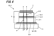


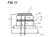

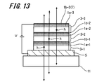

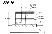


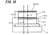
Classifications
-
- H—ELECTRICITY
- H10—SEMICONDUCTOR DEVICES; ELECTRIC SOLID-STATE DEVICES NOT OTHERWISE PROVIDED FOR
- H10K—ORGANIC ELECTRIC SOLID-STATE DEVICES
- H10K50/00—Organic light-emitting devices
- H10K50/10—OLEDs or polymer light-emitting diodes [PLED]
- H10K50/11—OLEDs or polymer light-emitting diodes [PLED] characterised by the electroluminescent [EL] layers
-
- C—CHEMISTRY; METALLURGY
- C07—ORGANIC CHEMISTRY
- C07D—HETEROCYCLIC COMPOUNDS
- C07D401/00—Heterocyclic compounds containing two or more hetero rings, having nitrogen atoms as the only ring hetero atoms, at least one ring being a six-membered ring with only one nitrogen atom
- C07D401/14—Heterocyclic compounds containing two or more hetero rings, having nitrogen atoms as the only ring hetero atoms, at least one ring being a six-membered ring with only one nitrogen atom containing three or more hetero rings
-
- C—CHEMISTRY; METALLURGY
- C07—ORGANIC CHEMISTRY
- C07D—HETEROCYCLIC COMPOUNDS
- C07D213/00—Heterocyclic compounds containing six-membered rings, not condensed with other rings, with one nitrogen atom as the only ring hetero atom and three or more double bonds between ring members or between ring members and non-ring members
- C07D213/02—Heterocyclic compounds containing six-membered rings, not condensed with other rings, with one nitrogen atom as the only ring hetero atom and three or more double bonds between ring members or between ring members and non-ring members having three double bonds between ring members or between ring members and non-ring members
- C07D213/04—Heterocyclic compounds containing six-membered rings, not condensed with other rings, with one nitrogen atom as the only ring hetero atom and three or more double bonds between ring members or between ring members and non-ring members having three double bonds between ring members or between ring members and non-ring members having no bond between the ring nitrogen atom and a non-ring member or having only hydrogen or carbon atoms directly attached to the ring nitrogen atom
- C07D213/06—Heterocyclic compounds containing six-membered rings, not condensed with other rings, with one nitrogen atom as the only ring hetero atom and three or more double bonds between ring members or between ring members and non-ring members having three double bonds between ring members or between ring members and non-ring members having no bond between the ring nitrogen atom and a non-ring member or having only hydrogen or carbon atoms directly attached to the ring nitrogen atom containing only hydrogen and carbon atoms in addition to the ring nitrogen atom
- C07D213/22—Heterocyclic compounds containing six-membered rings, not condensed with other rings, with one nitrogen atom as the only ring hetero atom and three or more double bonds between ring members or between ring members and non-ring members having three double bonds between ring members or between ring members and non-ring members having no bond between the ring nitrogen atom and a non-ring member or having only hydrogen or carbon atoms directly attached to the ring nitrogen atom containing only hydrogen and carbon atoms in addition to the ring nitrogen atom containing two or more pyridine rings directly linked together, e.g. bipyridyl
-
- C—CHEMISTRY; METALLURGY
- C07—ORGANIC CHEMISTRY
- C07D—HETEROCYCLIC COMPOUNDS
- C07D271/00—Heterocyclic compounds containing five-membered rings having two nitrogen atoms and one oxygen atom as the only ring hetero atoms
- C07D271/02—Heterocyclic compounds containing five-membered rings having two nitrogen atoms and one oxygen atom as the only ring hetero atoms not condensed with other rings
- C07D271/10—1,3,4-Oxadiazoles; Hydrogenated 1,3,4-oxadiazoles
- C07D271/107—1,3,4-Oxadiazoles; Hydrogenated 1,3,4-oxadiazoles with two aryl or substituted aryl radicals attached in positions 2 and 5
-
- C—CHEMISTRY; METALLURGY
- C07—ORGANIC CHEMISTRY
- C07D—HETEROCYCLIC COMPOUNDS
- C07D403/00—Heterocyclic compounds containing two or more hetero rings, having nitrogen atoms as the only ring hetero atoms, not provided for by group C07D401/00
- C07D403/02—Heterocyclic compounds containing two or more hetero rings, having nitrogen atoms as the only ring hetero atoms, not provided for by group C07D401/00 containing two hetero rings
- C07D403/10—Heterocyclic compounds containing two or more hetero rings, having nitrogen atoms as the only ring hetero atoms, not provided for by group C07D401/00 containing two hetero rings linked by a carbon chain containing aromatic rings
-
- C—CHEMISTRY; METALLURGY
- C07—ORGANIC CHEMISTRY
- C07D—HETEROCYCLIC COMPOUNDS
- C07D403/00—Heterocyclic compounds containing two or more hetero rings, having nitrogen atoms as the only ring hetero atoms, not provided for by group C07D401/00
- C07D403/02—Heterocyclic compounds containing two or more hetero rings, having nitrogen atoms as the only ring hetero atoms, not provided for by group C07D401/00 containing two hetero rings
- C07D403/12—Heterocyclic compounds containing two or more hetero rings, having nitrogen atoms as the only ring hetero atoms, not provided for by group C07D401/00 containing two hetero rings linked by a chain containing hetero atoms as chain links
-
- C—CHEMISTRY; METALLURGY
- C07—ORGANIC CHEMISTRY
- C07D—HETEROCYCLIC COMPOUNDS
- C07D403/00—Heterocyclic compounds containing two or more hetero rings, having nitrogen atoms as the only ring hetero atoms, not provided for by group C07D401/00
- C07D403/14—Heterocyclic compounds containing two or more hetero rings, having nitrogen atoms as the only ring hetero atoms, not provided for by group C07D401/00 containing three or more hetero rings
-
- C—CHEMISTRY; METALLURGY
- C07—ORGANIC CHEMISTRY
- C07D—HETEROCYCLIC COMPOUNDS
- C07D405/00—Heterocyclic compounds containing both one or more hetero rings having oxygen atoms as the only ring hetero atoms, and one or more rings having nitrogen as the only ring hetero atom
- C07D405/14—Heterocyclic compounds containing both one or more hetero rings having oxygen atoms as the only ring hetero atoms, and one or more rings having nitrogen as the only ring hetero atom containing three or more hetero rings
-
- C—CHEMISTRY; METALLURGY
- C07—ORGANIC CHEMISTRY
- C07D—HETEROCYCLIC COMPOUNDS
- C07D409/00—Heterocyclic compounds containing two or more hetero rings, at least one ring having sulfur atoms as the only ring hetero atoms
- C07D409/14—Heterocyclic compounds containing two or more hetero rings, at least one ring having sulfur atoms as the only ring hetero atoms containing three or more hetero rings
-
- C—CHEMISTRY; METALLURGY
- C07—ORGANIC CHEMISTRY
- C07D—HETEROCYCLIC COMPOUNDS
- C07D413/00—Heterocyclic compounds containing two or more hetero rings, at least one ring having nitrogen and oxygen atoms as the only ring hetero atoms
- C07D413/02—Heterocyclic compounds containing two or more hetero rings, at least one ring having nitrogen and oxygen atoms as the only ring hetero atoms containing two hetero rings
- C07D413/10—Heterocyclic compounds containing two or more hetero rings, at least one ring having nitrogen and oxygen atoms as the only ring hetero atoms containing two hetero rings linked by a carbon chain containing aromatic rings
-
- C—CHEMISTRY; METALLURGY
- C07—ORGANIC CHEMISTRY
- C07D—HETEROCYCLIC COMPOUNDS
- C07D413/00—Heterocyclic compounds containing two or more hetero rings, at least one ring having nitrogen and oxygen atoms as the only ring hetero atoms
- C07D413/14—Heterocyclic compounds containing two or more hetero rings, at least one ring having nitrogen and oxygen atoms as the only ring hetero atoms containing three or more hetero rings
-
- C—CHEMISTRY; METALLURGY
- C07—ORGANIC CHEMISTRY
- C07D—HETEROCYCLIC COMPOUNDS
- C07D471/00—Heterocyclic compounds containing nitrogen atoms as the only ring hetero atoms in the condensed system, at least one ring being a six-membered ring with one nitrogen atom, not provided for by groups C07D451/00 - C07D463/00
- C07D471/02—Heterocyclic compounds containing nitrogen atoms as the only ring hetero atoms in the condensed system, at least one ring being a six-membered ring with one nitrogen atom, not provided for by groups C07D451/00 - C07D463/00 in which the condensed system contains two hetero rings
- C07D471/04—Ortho-condensed systems
-
- C—CHEMISTRY; METALLURGY
- C07—ORGANIC CHEMISTRY
- C07D—HETEROCYCLIC COMPOUNDS
- C07D471/00—Heterocyclic compounds containing nitrogen atoms as the only ring hetero atoms in the condensed system, at least one ring being a six-membered ring with one nitrogen atom, not provided for by groups C07D451/00 - C07D463/00
- C07D471/12—Heterocyclic compounds containing nitrogen atoms as the only ring hetero atoms in the condensed system, at least one ring being a six-membered ring with one nitrogen atom, not provided for by groups C07D451/00 - C07D463/00 in which the condensed system contains three hetero rings
- C07D471/14—Ortho-condensed systems
-
- C—CHEMISTRY; METALLURGY
- C07—ORGANIC CHEMISTRY
- C07D—HETEROCYCLIC COMPOUNDS
- C07D491/00—Heterocyclic compounds containing in the condensed ring system both one or more rings having oxygen atoms as the only ring hetero atoms and one or more rings having nitrogen atoms as the only ring hetero atoms, not provided for by groups C07D451/00 - C07D459/00, C07D463/00, C07D477/00 or C07D489/00
- C07D491/02—Heterocyclic compounds containing in the condensed ring system both one or more rings having oxygen atoms as the only ring hetero atoms and one or more rings having nitrogen atoms as the only ring hetero atoms, not provided for by groups C07D451/00 - C07D459/00, C07D463/00, C07D477/00 or C07D489/00 in which the condensed system contains two hetero rings
- C07D491/04—Ortho-condensed systems
-
- C—CHEMISTRY; METALLURGY
- C07—ORGANIC CHEMISTRY
- C07D—HETEROCYCLIC COMPOUNDS
- C07D519/00—Heterocyclic compounds containing more than one system of two or more relevant hetero rings condensed among themselves or condensed with a common carbocyclic ring system not provided for in groups C07D453/00 or C07D455/00
-
- H—ELECTRICITY
- H10—SEMICONDUCTOR DEVICES; ELECTRIC SOLID-STATE DEVICES NOT OTHERWISE PROVIDED FOR
- H10K—ORGANIC ELECTRIC SOLID-STATE DEVICES
- H10K50/00—Organic light-emitting devices
- H10K50/10—OLEDs or polymer light-emitting diodes [PLED]
- H10K50/19—Tandem OLEDs
-
- H—ELECTRICITY
- H10—SEMICONDUCTOR DEVICES; ELECTRIC SOLID-STATE DEVICES NOT OTHERWISE PROVIDED FOR
- H10K—ORGANIC ELECTRIC SOLID-STATE DEVICES
- H10K50/00—Organic light-emitting devices
- H10K50/80—Constructional details
- H10K50/805—Electrodes
- H10K50/81—Anodes
- H10K50/816—Multilayers, e.g. transparent multilayers
-
- H—ELECTRICITY
- H10—SEMICONDUCTOR DEVICES; ELECTRIC SOLID-STATE DEVICES NOT OTHERWISE PROVIDED FOR
- H10K—ORGANIC ELECTRIC SOLID-STATE DEVICES
- H10K50/00—Organic light-emitting devices
- H10K50/80—Constructional details
- H10K50/805—Electrodes
- H10K50/82—Cathodes
- H10K50/828—Transparent cathodes, e.g. comprising thin metal layers
-
- H—ELECTRICITY
- H10—SEMICONDUCTOR DEVICES; ELECTRIC SOLID-STATE DEVICES NOT OTHERWISE PROVIDED FOR
- H10K—ORGANIC ELECTRIC SOLID-STATE DEVICES
- H10K59/00—Integrated devices, or assemblies of multiple devices, comprising at least one organic light-emitting element covered by group H10K50/00
- H10K59/80—Constructional details
- H10K59/805—Electrodes
- H10K59/8051—Anodes
- H10K59/80517—Multilayers, e.g. transparent multilayers
-
- H—ELECTRICITY
- H10—SEMICONDUCTOR DEVICES; ELECTRIC SOLID-STATE DEVICES NOT OTHERWISE PROVIDED FOR
- H10K—ORGANIC ELECTRIC SOLID-STATE DEVICES
- H10K59/00—Integrated devices, or assemblies of multiple devices, comprising at least one organic light-emitting element covered by group H10K50/00
- H10K59/80—Constructional details
- H10K59/805—Electrodes
- H10K59/8052—Cathodes
- H10K59/80524—Transparent cathodes, e.g. comprising thin metal layers
-
- H—ELECTRICITY
- H10—SEMICONDUCTOR DEVICES; ELECTRIC SOLID-STATE DEVICES NOT OTHERWISE PROVIDED FOR
- H10K—ORGANIC ELECTRIC SOLID-STATE DEVICES
- H10K85/00—Organic materials used in the body or electrodes of devices covered by this subclass
- H10K85/60—Organic compounds having low molecular weight
- H10K85/649—Aromatic compounds comprising a hetero atom
- H10K85/654—Aromatic compounds comprising a hetero atom comprising only nitrogen as heteroatom
-
- H—ELECTRICITY
- H10—SEMICONDUCTOR DEVICES; ELECTRIC SOLID-STATE DEVICES NOT OTHERWISE PROVIDED FOR
- H10K—ORGANIC ELECTRIC SOLID-STATE DEVICES
- H10K85/00—Organic materials used in the body or electrodes of devices covered by this subclass
- H10K85/60—Organic compounds having low molecular weight
- H10K85/649—Aromatic compounds comprising a hetero atom
- H10K85/657—Polycyclic condensed heteroaromatic hydrocarbons
- H10K85/6572—Polycyclic condensed heteroaromatic hydrocarbons comprising only nitrogen in the heteroaromatic polycondensed ring system, e.g. phenanthroline or carbazole
-
- H—ELECTRICITY
- H10—SEMICONDUCTOR DEVICES; ELECTRIC SOLID-STATE DEVICES NOT OTHERWISE PROVIDED FOR
- H10K—ORGANIC ELECTRIC SOLID-STATE DEVICES
- H10K85/00—Organic materials used in the body or electrodes of devices covered by this subclass
- H10K85/60—Organic compounds having low molecular weight
- H10K85/649—Aromatic compounds comprising a hetero atom
- H10K85/657—Polycyclic condensed heteroaromatic hydrocarbons
- H10K85/6574—Polycyclic condensed heteroaromatic hydrocarbons comprising only oxygen in the heteroaromatic polycondensed ring system, e.g. cumarine dyes
-
- H—ELECTRICITY
- H10—SEMICONDUCTOR DEVICES; ELECTRIC SOLID-STATE DEVICES NOT OTHERWISE PROVIDED FOR
- H10K—ORGANIC ELECTRIC SOLID-STATE DEVICES
- H10K85/00—Organic materials used in the body or electrodes of devices covered by this subclass
- H10K85/60—Organic compounds having low molecular weight
- H10K85/649—Aromatic compounds comprising a hetero atom
- H10K85/657—Polycyclic condensed heteroaromatic hydrocarbons
- H10K85/6576—Polycyclic condensed heteroaromatic hydrocarbons comprising only sulfur in the heteroaromatic polycondensed ring system, e.g. benzothiophene
-
- H—ELECTRICITY
- H10—SEMICONDUCTOR DEVICES; ELECTRIC SOLID-STATE DEVICES NOT OTHERWISE PROVIDED FOR
- H10K—ORGANIC ELECTRIC SOLID-STATE DEVICES
- H10K59/00—Integrated devices, or assemblies of multiple devices, comprising at least one organic light-emitting element covered by group H10K50/00
- H10K59/30—Devices specially adapted for multicolour light emission
- H10K59/32—Stacked devices having two or more layers, each emitting at different wavelengths
-
- H—ELECTRICITY
- H10—SEMICONDUCTOR DEVICES; ELECTRIC SOLID-STATE DEVICES NOT OTHERWISE PROVIDED FOR
- H10K—ORGANIC ELECTRIC SOLID-STATE DEVICES
- H10K85/00—Organic materials used in the body or electrodes of devices covered by this subclass
- H10K85/10—Organic polymers or oligomers
- H10K85/151—Copolymers
Definitions
- the present invention relates to an organic electroluminescent device, and more particularly, to an organic electroluminescent device having a tandem structure in which a plurality of light emitting units each having a light emitting layer formed using an organic material are stacked.
- An organic electroluminescent element (so-called organic EL element) using electroluminescence (hereinafter referred to as EL) of an organic material has a trade-off relationship between luminous efficiency and driving life. For this reason, a light emitting functional layer including a light emitting layer composed of an organic material is used as one light emitting unit, and a plurality of light emitting units are stacked through an intermediate layer, thereby extending the life while ensuring luminous efficiency.
- a tandem structure has been proposed. As the intermediate layer in such a tandem structure, for example, the following Patent Documents 1 to 6 disclose each configuration.
- Patent Document 1 discloses a configuration in which a conductive layer containing magnesium (Mg) as a main component and containing silver (Ag) is used in a floating state.
- Patent Document 2 a metal layer having a small work function such as Mg, Mg / Ag, and arsenic (As), indium tin oxide (SnO 2 —In 2 O 3 : Indium Tin Oxide: ITO) The structure which uses this laminated body as an intermediate electrode is disclosed.
- Patent Document 3 a structure in which a charge generation layer formed of an electrically insulating layer is used as an intermediate layer, or a hole injection layer doped with an electron accepting compound is used as an intermediate layer in contact with the cathode side of the charge generation layer.
- the structure to be formed is disclosed.
- Patent Document 4 discloses an intermediate layer in which the composition ratio of an additive (electron donating property or electron attracting property) in an inorganic or organic semiconductor material is changed in the film thickness direction.
- Patent Document 5 discloses a configuration in which three layers of an electron injection layer, a metal-organic mixed layer (for example, Ag—Alq3), and a hole injection layer are stacked to form an intermediate layer.
- Patent Document 6 a transparent conductive film such as ITO is used as a charge generation layer (that is, an intermediate layer), and etching of a benzoxazole derivative, a pyridine derivative, or the like is performed on the electroluminescent layer closest to the previous charge generation layer.
- a transparent conductive film such as ITO is used as a charge generation layer (that is, an intermediate layer)
- etching of a benzoxazole derivative, a pyridine derivative, or the like is performed on the electroluminescent layer closest to the previous charge generation layer.
- an object of the present invention is to provide an organic electroluminescent element having a tandem structure capable of achieving both improvement in luminous efficiency and improvement in lifetime characteristics.
- An organic electroluminescent device disposed adjacent to the substrate.
- Y5 represents a divalent linking group composed of an arylene group, a heteroarylene group, or a combination thereof.
- E51 to E66 and E71 to E88 each represent —C (R3) ⁇ or —N ⁇ , and R3 represents a hydrogen atom or a substituent.
- n3 and n4 represent an integer of 0 to 4, and n3 + n4 is an integer of 2 or more.
- R21 represents a substituent
- R22 represents a hydrogen atom (H) or a substituent
- the organic electroluminescent element of the present invention configured as described above uses a transparent conductive layer using silver or an alloy containing silver as a main component as a conductive layer between electrodes or light emitting units.
- a transparent conductive layer using silver or an alloy containing silver as a main component as a conductive layer between electrodes or light emitting units.
- it is the structure which made the nitrogen containing layer comprised using the compound containing a nitrogen atom adjoined.
- the silver atoms constituting the transparent conductive layer interact with the compound containing nitrogen atoms constituting the nitrogen-containing layer, and The diffusion distance on the surface of the nitrogen-containing layer is reduced and silver aggregation is suppressed.
- a silver thin film that is easily isolated in an island shape by film growth of a nuclear growth type (Volume-Weber: VW type) is a single-layer growth type (Frank-van der Merwe: FM type).
- a film is formed. Therefore, a transparent conductive layer having a uniform film thickness can be obtained even though the film thickness is small.
- the transparent conductive layer having ensured conductivity can be used as the conductive layer between the electrodes or the light emitting units while maintaining the light transmittance as a thinner film thickness, It is possible to achieve both improvement in luminous efficiency and improvement in lifetime characteristics in an organic electroluminescent element having a tandem structure.
- FIG. 4 is a graph showing the relationship between effective action energy ⁇ Eef and sheet resistance in the transparent electrode produced in Example 1.
- 4 is a schematic cross-sectional view showing a configuration of an organic electroluminescent element produced in Example 2.
- FIG. 6 is a schematic cross-sectional view showing a configuration of a comparative example of Example 2.
- FIG. 6 is a schematic cross-sectional view showing the configuration of an organic electroluminescent element produced in Example 3.
- FIG. 6 is a schematic cross-sectional view showing a configuration of a comparative example of Example 3.
- FIG. 6 is a schematic cross-sectional view showing the configuration of an organic electroluminescent element produced in Example 4.
- FIG. 6 is a schematic cross-sectional view showing a configuration of a comparative example of Example 4.
- FIG. 6 is a schematic cross-sectional view showing a configuration of an organic electroluminescent element produced in Example 5.
- FIG. 6 is a schematic cross-sectional view showing a configuration of an organic electroluminescent element produced in Example 6.
- FIG. 1 is a schematic cross-sectional view showing a configuration of a transparent conductive layer used in an organic electroluminescent device having a tandem structure.
- the transparent conductive layer 1b is characterized by being provided adjacent to the nitrogen-containing layer 1a.
- the transparent conductive layer 1b is made of silver (Ag) or an alloy containing silver as a main component.
- the nitrogen-containing layer 1a is composed of a compound containing a nitrogen atom, and the effective action energy ⁇ Eef described below has a specific relationship with silver, which is the main material constituting the transparent conductive layer 1b. It is the layer comprised using the compound which has.
- the nitrogen-containing layer 1a is a layer formed using a compound having a specific relationship with silver (Ag), which is the main material constituting the transparent conductive layer 1b, among the compounds containing nitrogen atoms.
- the effective action energy ⁇ Eef represented by the following formula (1) is defined as the energy that interacts between the compound and silver.
- this effective action energy (DELTA) Eef comprises the nitrogen-containing layer 1a using the compound which has the specific relationship which satisfy
- the number of nitrogen atoms in the compound that stably binds to silver [n] is selected from the nitrogen atoms contained in the compound as the specific nitrogen atom only from the nitrogen atoms that stably bind to silver Is the number counted.
- the nitrogen atoms to be selected are all nitrogen atoms contained in the compound, and are not limited to the nitrogen atoms constituting the heterocyclic ring.
- the selection of a specific nitrogen atom out of all the nitrogen atoms contained in such a compound is, for example, the bond distance [r (Ag ⁇ Ag ⁇ N)] is used as an index, or the angle formed between the nitrogen atom and silver relative to the ring containing the nitrogen atom in the compound, that is, the dihedral angle [D] is used as an index.
- the molecular orbital calculation is performed using, for example, Gaussian 03 (Gaussian, Inc., Wallingford, CT, 2003).
- the bond distance [r (Ag ⁇ N)] is used as an index, considering the steric structure of each compound, the distance at which the nitrogen atom and silver are stably bonded in the compound is expressed as “stable bond distance”. ”Is set. Then, for each nitrogen atom contained in the compound, a bond distance [r (Ag ⁇ N)] is calculated using a molecular orbital calculation method. A nitrogen atom having a calculated bond distance [r (Ag ⁇ N)] close to the “stable bond distance” is selected as a specific nitrogen atom. Such selection of a nitrogen atom is applied to a compound containing many nitrogen atoms constituting a heterocyclic ring and a compound containing many nitrogen atoms not constituting a heterocyclic ring.
- the dihedral angle [D] When the dihedral angle [D] is used as an index, the dihedral angle [D] described above is calculated using a molecular orbital calculation method. Then, a nitrogen atom whose calculated dihedral angle [D] satisfies D ⁇ 10 degrees is selected as a specific nitrogen atom. Such selection of a nitrogen atom is applied to a compound containing a large number of nitrogen atoms constituting a heterocyclic ring.
- the interaction energy [ ⁇ E] between silver (Ag) and nitrogen (N) in the compound can be calculated by a molecular orbital calculation method, and the mutual energy between nitrogen and silver selected as described above. The energy of action.
- the surface area [s] is calculated for the optimized structure using Tencube / WM (manufactured by Tencube Co., Ltd.).
- the effective action energy ⁇ Eef defined as described above is in a range satisfying the following formula (3).
- a compound containing a nitrogen atom constituting the nitrogen-containing layer 1a for example, a compound containing a heterocyclic ring having a nitrogen atom (N) as a hetero atom is used.
- Heterocycles having a nitrogen atom (N) as a hetero atom include aziridine, azirine, azetidine, azeto, azolidine, azole, azinane, pyridine, azepane, azepine, imidazole, pyrazole, oxazole, thiazole, imidazoline, pyrazine, pyridazine, pyrimidine Morpholine, thiazine, indole, isoindole, benzimidazole, purine, quinoline, isoquinoline, quinoxaline, cinnoline, pteridine, acridine, carbazole, benzo-C-cinnoline, porphyrin, chlorin
- the compound preferably used is, for example, a compound represented by the following general formula (1) or a compound represented by the following general formula (2). Is done.
- the nitrogen-containing layer 1a provided adjacent to the transparent conductive layer 1b is selected from compounds represented by the above formula (1) or formula (2) among these general formulas (1) or (2). ) Is selected and used.
- Y5 represents a divalent linking group composed of an arylene group, a heteroarylene group, or a combination thereof.
- E51 to E66 and E71 to E88 each represent —C (R3) ⁇ or —N ⁇ , and R3 represents a hydrogen atom or a substituent.
- R3 represents a hydrogen atom or a substituent.
- n3 and n4 represent an integer of 0 to 4
- n3 + n4 is an integer of 2 or more.
- examples of the arylene group represented by Y5 include an o-phenylene group, a p-phenylene group, a naphthalenediyl group, an anthracenediyl group, a naphthacenediyl group, a pyrenediyl group, a naphthylnaphthalenediyl group, and a biphenyldiyl group.
- examples of the heteroarylene group represented by Y5 include a carbazole ring, a carboline ring, a diazacarbazole ring (also referred to as a monoazacarboline ring, and one of the carbon atoms constituting the carboline ring is nitrogen.
- the ring structure is replaced by an atom), a triazole ring, a pyrrole ring, a pyridine ring, a pyrazine ring, a quinoxaline ring, a thiophene ring, an oxadiazole ring, a dibenzofuran ring, a dibenzothiophene ring, and an indole ring.
- a triazole ring such as a pyrrole ring, a pyridine ring, a pyrazine ring, a quinoxaline ring, a thiophene ring, an oxadiazole ring, a dibenzo
- the divalent linking group comprising an arylene group, a heteroarylene group or a combination thereof represented by Y5
- a condensed aromatic heterocycle formed by condensation of three or more rings among the heteroarylene groups, a condensed aromatic heterocycle formed by condensation of three or more rings.
- a group derived from a condensed aromatic heterocycle formed by condensation of three or more rings is preferably included, and the group derived from a dibenzofuran ring or a dibenzothiophene ring is preferable.
- Y5 a condensed aromatic heterocycle formed by condensation of three or more rings.
- a group derived from a condensed aromatic heterocycle formed by condensation of three or more rings is preferably included, and the group derived from a dibenzofuran ring or a dibenzothiophene ring is preferable.
- examples of the substituent represented by R3 of —C (R3) ⁇ represented by E51 to E66 and E71 to E88, respectively, include an alkyl group (for example, methyl group, ethyl group, propyl group) Group, isopropyl group, tert-butyl group, pentyl group, hexyl group, octyl group, dodecyl group, tridecyl group, tetradecyl group, pentadecyl group, etc.), cycloalkyl group (for example, cyclopentyl group, cyclohexyl group etc.), alkenyl group ( For example, vinyl group, allyl group, etc.), alkynyl group (for example, ethynyl group, propargyl group, etc.), aromatic hydrocarbon group (aromatic carbocyclic group, aryl group, etc.), for example, phenyl group, p-chloroph
- substituents may be further substituted with the above substituents.
- a plurality of these substituents may be bonded to each other to form a ring.
- E71 to E74 and E80 to E83 are each represented by —C (R3) ⁇ .
- E53 is represented by —C (R3) ⁇ and R3 represents a linking site
- E61 is also represented by —C (R3) ⁇ .
- R3 preferably represents a linking site.
- R21 represents a substituent.
- R22 represents a hydrogen atom (H) or a substituent.
- examples of the substituents represented by R21 and R22 include those similar to R3 in the general formula (1). Some of these substituents may be further substituted with the above substituents.
- the film forming method may be a method using a wet process such as a coating method, an ink jet method, a coating method, a dip method, or vapor deposition.
- a method using a dry process such as a method (resistance heating, EB method, etc.), a sputtering method, or a CVD method.
- the vapor deposition method is preferably applied.
- Specific examples (1 to 134) of the compounds constituting the nitrogen-containing layer 1a are shown below, but are not limited thereto.
- the compound which is not contained in the said General formula (1) and General formula (2) here is illustrated here.
- the nitrogen-containing layer 1a provided adjacent to the transparent conductive layer 1b is composed of compounds (1) to (134) exemplified below that are compounds that fall within the above formula (1) or (2). Select and use.
- Step 1 (Synthesis of Intermediate 1) Under a nitrogen atmosphere, 2,8-dibromodibenzofuran (1.0 mol), carbazole (2.0 mol), copper powder (3.0 mol), potassium carbonate (1.5 mol), DMAc (dimethylacetamide) 300 ml Mixed in and stirred at 130 ° C. for 24 hours.
- Step 2 (Synthesis of Intermediate 2)
- Intermediate 1 (0.5 mol) was dissolved in 100 ml of DMF (dimethylformamide) at room temperature in the atmosphere, NBS (N-bromosuccinimide) (2.0 mol) was added, and the mixture was stirred overnight at room temperature. The resulting precipitate was filtered and washed with methanol, yielding intermediate 2 in 92% yield.
- Step 3 (Synthesis of Compound 5) Under a nitrogen atmosphere, intermediate 2 (0.25 mol), 2-phenylpyridine (1.0 mol), ruthenium complex [( ⁇ 6 -C 6 H 6 ) RuCl 2 ] 2 (0.05 mol), triphenyl Phosphine (0.2 mol) and potassium carbonate (12 mol) were mixed in 3 L of NMP (N-methyl-2-pyrrolidone) and stirred at 140 ° C. overnight.
- NMP N-methyl-2-pyrrolidone
- the transparent conductive layer 1b is a layer formed using silver or an alloy containing silver as a main component, and is a layer formed adjacent to the nitrogen-containing layer 1a.
- the transparent conductive layer 1b is composed of silver (Ag)
- Ag is included at 98 atms% or more.
- the transparent conductive layer 1b is comprised with the alloy which has silver (Ag) as a main component, it shall contain 50 atms% or more of silver (Ag).
- Metals used in combination with silver (Ag) are aluminum (Al), indium (In), tin (Sn), copper (Cu), palladium (Pd), gold (Au), platinum (Pt), magnesium (Mg) ) Etc.
- the transparent conductive layer 1b as described above may have a structure in which silver or an alloy layer mainly composed of silver is divided into a plurality of layers as necessary.
- the transparent conductive layer 1b preferably has a thickness in the range of 4 to 12 nm.
- the film thickness of 12 nm or less is preferable because the absorption component or reflection component of the layer can be kept low and the light transmittance of the transparent conductive layer can be maintained.
- the electroconductivity of a layer is also ensured because a film thickness is 4 nm or more.
- a method for forming such a transparent conductive layer 1b a method using a wet process such as a coating method, an ink jet method, a coating method, a dip method, a vapor deposition method (resistance heating, EB method, etc.), a sputtering method, or a CVD method is used. And a method using a dry process such as Of these, the vapor deposition method is preferably applied.
- the transparent conductive layer 1b is formed on the nitrogen-containing layer 1a so that it has sufficient conductivity even without high-temperature annealing after the film formation, etc. It may be one that has been subjected to high-temperature annealing after film formation.
- the transparent conductive layer 1b configured as described above is provided using silver or an alloy containing silver as a main component adjacent to the nitrogen-containing layer 1a configured using a compound containing nitrogen atoms. It is.
- the silver atoms constituting the transparent conductive layer 1b interact with the compound containing nitrogen atoms constituting the nitrogen-containing layer 1a.
- the diffusion distance of silver atoms on the surface of the nitrogen-containing layer 1a is reduced, and aggregation of silver is suppressed.
- a silver thin film that is easily isolated in an island shape by film growth of a nuclear growth type is a single layer growth type (Frank-van der Merwe: FM type) film growth.
- a film is formed. Therefore, the transparent conductive layer 1b having a uniform film thickness can be obtained even though the film thickness is small.
- the effective action energy ⁇ Eef shown in the above formula (1) is defined as the energy that interacts between the compound that forms the nitrogen-containing layer 1a and the silver that forms the transparent conductive layer 1b.
- the nitrogen-containing layer 1a was formed using a compound satisfying ⁇ 0.5 ⁇ ⁇ Eef ⁇ ⁇ 0.10. This makes it possible to form the nitrogen-containing layer 1a using a compound that can reliably obtain the effect of “suppressing the aggregation of silver” as described above. This is because, as will be described in detail in a later embodiment, on such a nitrogen-containing layer 1a, there is a transparent conductive layer 1b that can measure sheet resistance by the four-probe method while being an extremely thin film. It was also confirmed from the formation.
- the transparent conductive layer 1b which is adjacent to such a nitrogen-containing layer 1a and has a uniform film thickness while ensuring light transmission while having a thin film thickness is ensured. Therefore, it is possible to achieve both improvement in conductivity and improvement in light transmission in the transparent conductive layer 1b using silver.
- Such a transparent conductive layer 1b is low-cost because it does not use indium (In), which is a rare metal, as a main component, and long-term reliability because it does not use a chemically unstable material such as ZnO. Also excellent.
- the transparent conductive layer 1b having the above-described configuration is not limited to application to an organic electroluminescent element as described below, and can be used for various electronic devices.
- electronic devices include organic electroluminescent elements, LEDs (light-emitting diodes), liquid crystal elements, solar cells, touch panels, etc.
- the electrode layers having light transmissivity are described above.
- a transparent conductive layer 1b disposed adjacent to the nitrogen-containing layer 1a can be used.
- FIG. 2 is a cross-sectional configuration diagram showing a first embodiment of an organic electroluminescent element having a tandem structure using the above-described transparent conductive layer 1b.
- the configuration of the organic electroluminescent element EL-1 will be described below based on this drawing.
- the organic electroluminescent element EL-1 shown in FIG. 2 is provided on the substrate 11, and in order from the substrate 11 side, the first electrode 5, the first light emitting unit 3-1, the nitrogen-containing layer 1a, and the transparent conductive material.
- the layer 1b, the second light emitting unit 3-2, and the second electrode 7 are stacked in this order.
- the organic electroluminescent element EL-1 is characterized in that the laminate of the nitrogen-containing layer 1a and the transparent conductive layer 1b described above is sandwiched between the two light emitting units 3-1, 3-2. It is.
- the details of the main layers constituting the organic electroluminescent element EL-1 are as follows: substrate 11, first electrode 5 and second electrode 7, nitrogen-containing layer 1a and transparent conductive layer 1b, and light emitting units 3-1, 3-2.
- the other components and the method for manufacturing the organic electroluminescent element will be described in this order.
- Substrate 11 Examples of the substrate 11 on which the organic electroluminescent element EL-1 is provided include, but are not limited to, glass and plastic.
- the substrate 11 may be transparent or opaque.
- the organic electroluminescent element EL-1 is a bottom emission type in which light is extracted from the substrate 11 side, the substrate 11 is preferably transparent.
- the transparent substrate 11 preferably used include glass, quartz, and a transparent resin film.
- the glass examples include silica glass, soda lime silica glass, lead glass, borosilicate glass, and alkali-free glass. From the viewpoints of adhesion, durability, and smoothness with the nitrogen-containing layer 1a, the surface of these glass materials is subjected to physical treatment such as polishing, a coating made of an inorganic material or an organic material, if necessary, A hybrid film combining these films is formed.
- polyesters such as polyethylene terephthalate (PET) and polyethylene naphthalate (PEN), polyethylene, polypropylene, cellophane, cellulose diacetate, cellulose triacetate, cellulose acetate butyrate, cellulose acetate propionate (CAP), Cellulose esters such as cellulose acetate phthalate (TAC) and cellulose nitrate or derivatives thereof, polyvinylidene chloride, polyvinyl alcohol, polyethylene vinyl alcohol, syndiotactic polystyrene, polycarbonate, norbornene resin, polymethylpentene, polyether ketone, polyimide , Polyethersulfone (PES), polyphenylene sulfide, polysulfone , Polyetherimide, polyetherketoneimide, polyamide, fluororesin, nylon, polymethylmethacrylate, acrylic or polyarylates, cyclone resins such as Arton (trade name JSR) or Appel (trade name Mits
- a film made of an inorganic material or an organic material or a hybrid film combining these films may be formed on the surface of the resin film.
- Such coatings and hybrid coatings have a water vapor transmission rate (25 ⁇ 0.5 ° C., relative humidity 90 ⁇ 2% RH) of 0.01 g / (measured by a method in accordance with JIS-K-7129-1992. m 2 ⁇ 24 hours) or less of a barrier film (also referred to as a barrier film or the like) is preferable.
- the oxygen permeability measured by a method according to JIS-K-7126-1987 is 10 ⁇ 3 ml / (m 2 ⁇ 24 hours ⁇ atm) or less, and the water vapor permeability is 10 ⁇ 5 g / (m 2 ⁇ 24 hours) or less high barrier film is preferable.
- the material for forming the barrier film as described above may be any material that has a function of suppressing intrusion of elements that cause deterioration of elements such as moisture and oxygen.
- silicon oxide, silicon dioxide, silicon nitride, or the like is used. be able to.
- the method for forming the barrier film is not particularly limited.
- the vacuum deposition method, the sputtering method, the reactive sputtering method, the molecular beam epitaxy method, the cluster ion beam method, the ion plating method, the plasma polymerization method, the atmospheric pressure plasma weighting can be used, but an atmospheric pressure plasma polymerization method described in JP-A No. 2004-68143 is particularly preferable.
- the substrate 11 is opaque, for example, a metal substrate such as aluminum or stainless steel, a film, an opaque resin substrate, a ceramic substrate, or the like can be used.
- First electrode 5 and second electrode 7 One of the first electrode 5 and the second electrode 7 functions as an anode for supplying holes to the light emitting units 3-1, 3-2, and either one of the first electrode 5 and the second electrode 7 is a light emitting unit 3-1, 3-2. It functions as a cathode for supplying electrons to.
- the first electrode 5 on the substrate 11 side is an anode
- the second electrode 7 opposite thereto is a cathode.
- the first electrode 5 and the second electrode 7 are electrode layers in which at least one or both functions as a transparent electrode.
- the first electrode 5 on the substrate 11 side is configured as a transparent electrode
- the emitted light h generated by the light emitting units 3-1 and 3-2 is extracted from the substrate 11 side, and this organic electroluminescent element EL ⁇ 1 is the bottom emission type.
- the second electrode 7 is configured as a transparent electrode
- the emitted light h generated by the light emitting units 3-1 and 3-2 is extracted from the side opposite to the substrate 11, and the organic electroluminescent element EL- 1 is Top emission type.
- the other electrode may be an electrode film that functions as a reflective electrode.
- the organic electroluminescent element EL-1 is a double-sided light emitting type.
- the first electrode 5 is configured as a transparent electrode.
- a metal, an alloy, an organic or inorganic conductive compound, and a mixture thereof are used for the first electrode 5 and the second electrode 7 as described above. Specifically, gold, aluminum, silver, magnesium, lithium, magnesium / copper mixture, magnesium / silver mixture, magnesium / aluminum mixture, magnesium / indium mixture, indium, lithium / aluminum mixture, rare earth metal, ITO, ZnO, TiO 2 and oxide semiconductors such as SnO 2 .
- the first electrode 5 and the second electrode 7 are configured by selecting a material suitable as a cathode material or an anode material from these materials.
- the electrode on the light extraction side (here, the first electrode) is composed of a material having good light transmittance among these materials.
- a material having good light transmittance among these materials include oxide semiconductors such as ITO, ZnO, TiO 2 , and SnO 2 .
- the first electrode 5 and the second electrode 7 may have a laminated structure as necessary. In such a configuration, only a portion where the light emitting units 3-1 and 3-2 are sandwiched between the first electrode 5 and the second electrode 7 becomes a light emitting region in the organic electroluminescent element EL-1.
- the first electrode 5 and the second electrode 7 as described above can be produced by forming a thin film from these conductive materials by a method such as vapor deposition or sputtering.
- the sheet resistance as the first electrode 5 and the second electrode 7 is preferably several hundred ⁇ / ⁇ or less, and the film thickness is usually selected in the range of 5 nm to 5 ⁇ m, preferably 5 nm to 200 nm.
- a vapor deposition method is applied to the second electrode at the top of the light emitting unit 3-2.
- the nitrogen-containing layer 1a and the transparent conductive layer 1b have the structures described above.
- the nitrogen-containing layer 1a and the transparent conductive layer 1b are arranged in this order from the substrate 11 side.
- the transparent conductive layer 1b functions as a cathode for the light emitting unit 3-1 on the first electrode (anode) 5 side, It functions as an anode for the light emitting unit 3-2 on the two-electrode (cathode) 7 side.
- the nitrogen-containing layer 1a sandwiched between the light emitting unit 3-1 and the transparent conductive layer 1b is also regarded as a layer constituting a part of the light emitting unit 3-1.
- the transparent conductive layer 1b functions as a cathode for the light emitting unit 3-1
- the nitrogen-containing layer 1a sandwiched between them is a material that satisfies the above-described formula (1) or (2).
- such a nitrogen-containing layer 1a may be configured using a material satisfying the formula (1) or the formula (2) among the materials exemplified as an electron transport material hereinafter.
- the nitrogen-containing layer 1a When the nitrogen-containing layer 1a is used as a layer having an electron transport property or an electron injection property as described above, the nitrogen-containing layer 1a includes an alkali metal, an alkali metal salt, an alkaline earth metal, or an alkaline earth metal salt. Etc. can also be mixed and contained. Specific examples include metals such as lithium, potassium, sodium, cesium, magnesium, calcium, and strontium, and salts thereof. As a method of mixing and adding, preferred is co-evaporation with a nitrogen-containing compound. Thereby, the moving speed to the light emitting layer of the electron inject
- the transparent conductive layer 1b functions as an anode for the light emitting unit 3-1 on the first electrode (cathode) 5 side.
- the nitrogen-containing layer 1a between the transparent conductive layer 1b and the light emitting unit 3-1 is preferably configured using a material having a hole transporting property or a hole injecting property.
- the overall layer structure of the light emitting units 3-1 and 3-2 is not limited, and each may have a general layer structure.
- a configuration in which [hole injection layer / hole transport layer / light emitting layer / electron transport layer / electron injection layer] is stacked in order from the anode side is exemplified, and among these, at least an organic material is used. It is essential to have a light emitting layer.
- the hole injection layer and the hole transport layer may be provided as a hole transport / injection layer.
- the electron transport layer and the electron injection layer may be provided as an electron transport / injection layer.
- the electron injection layer may be composed of an inorganic material.
- the light emitting units 3-1 and 3-2 may have a hole blocking layer, an electron blocking layer, and the like laminated at necessary places as necessary.
- the light emitting layer may have each color light emitting layer for generating emitted light in each wavelength region, and each color light emitting layer may be laminated through a non-light emitting intermediate layer to form a light emitting layer unit.
- the intermediate layer may function as a hole blocking layer and an electron blocking layer.
- the light emitting units 3-1 and 3-2 may be configured to obtain the same color of emitted light h, or may be configured to obtain different colors of emitted light h.
- each layer constituting the light emitting units 3-1 and 3-2 will be described in the order of the light emitting layer, the injection layer, the hole transport layer, the electron transport layer, and the blocking layer.
- the light emitting layer used in the present invention contains, for example, a phosphorescent light emitting compound as a light emitting material.
- This light emitting layer is a layer that emits light by recombination of electrons injected from the electrode or the electron transport layer and holes injected from the hole transport layer, and the light emitting portion is in the layer of the light emitting layer. Alternatively, it may be the interface between the light emitting layer and the adjacent layer.
- Such a light emitting layer is not particularly limited in its configuration as long as the light emitting material contained satisfies the light emission requirements. Moreover, there may be a plurality of layers having the same emission spectrum and emission maximum wavelength. In this case, it is preferable to have a non-light emitting intermediate layer (not shown) between the light emitting layers.
- the total film thickness of the light emitting layer is preferably in the range of 1 to 100 nm, and more preferably 1 to 30 nm because a lower driving voltage can be obtained. Note that the total film thickness of the light emitting layer is a film thickness including the intermediate layer when a non-light emitting intermediate layer exists between the light emitting layers.
- the film thickness of each light emitting layer is preferably adjusted to a range of 1 to 50 nm, more preferably adjusted to a range of 1 to 20 nm.
- the plurality of stacked light emitting layers correspond to blue, green, and red light emitting colors, there is no particular limitation on the relationship between the film thicknesses of the blue, green, and red light emitting layers.
- the light emitting layer as described above is formed by forming a light emitting material or a host compound described later by a known thin film forming method such as a vacuum deposition method, a spin coating method, a casting method, an LB method, or an ink jet method. Can do.
- a plurality of light emitting materials may be mixed, and a phosphorescent light emitting material and a fluorescent light emitting material (also referred to as a fluorescent dopant or a fluorescent compound) may be mixed and used in the same light emitting layer.
- a phosphorescent light emitting material and a fluorescent light emitting material also referred to as a fluorescent dopant or a fluorescent compound
- the structure of the light emitting layer preferably contains a host compound (also referred to as a light emitting host or the like) and a light emitting material (also referred to as a light emitting dopant compound) and emits light from the light emitting material.
- a host compound also referred to as a light emitting host or the like
- a light emitting material also referred to as a light emitting dopant compound
- a compound having a phosphorescence quantum yield of phosphorescence emission at room temperature (25 ° C.) of less than 0.1 is preferable. More preferably, the phosphorescence quantum yield is less than 0.01. Moreover, it is preferable that the volume ratio in the layer is 50% or more among the compounds contained in a light emitting layer.
- a known host compound may be used alone, or a plurality of types may be used. By using a plurality of types of host compounds, it is possible to adjust the movement of charges, and the efficiency of the organic electroluminescent element EL-1 can be increased. In addition, by using a plurality of kinds of light emitting materials described later, it is possible to mix different light emission, thereby obtaining an arbitrary light emission color.
- the host compound used may be a conventionally known low molecular compound, a high molecular compound having a repeating unit, or a low molecular compound having a polymerizable group such as a vinyl group or an epoxy group (evaporation polymerizable light emitting host). .
- the known host compound a compound having a hole transporting ability and an electron transporting ability, preventing an increase in the wavelength of light emission and having a high Tg (glass transition temperature) is preferable.
- the glass transition point (Tg) here is a value determined by a method based on JIS-K-7121 using DSC (Differential Scanning Colorimetry).
- H1 to H79 Specific examples (H1 to H79) of host compounds that can be used in the present invention are shown below, but are not limited thereto.
- a phosphorescent compound As a light-emitting material that can be used in the present invention, a phosphorescent compound (also referred to as a phosphorescent compound or a phosphorescent material) can be given.
- a phosphorescent compound is a compound in which light emission from an excited triplet is observed. Specifically, a phosphorescent compound emits phosphorescence at room temperature (25 ° C.), and a phosphorescence quantum yield of 0.01 at 25 ° C. Although defined as the above compounds, the preferred phosphorescence quantum yield is 0.1 or more.
- the phosphorescent quantum yield can be measured by the method described in Spectra II, page 398 (1992 version, Maruzen) of Experimental Chemistry Course 4 of the 4th edition. Although the phosphorescence quantum yield in a solution can be measured using various solvents, when using a phosphorescent compound in the present invention, the above phosphorescence quantum yield (0.01 or more) is achieved in any solvent. It only has to be done.
- phosphorescent compounds There are two types of light emission principles of phosphorescent compounds. One is that recombination of carriers occurs on the host compound to which carriers are transported to generate an excited state of the host compound, and this energy is transferred to the phosphorescent compound to obtain light emission from the phosphorescent compound.
- the other is a carrier trap type in which the phosphorescent compound becomes a carrier trap, and carriers are recombined on the phosphorescent compound to emit light from the phosphorescent compound. In any case, it is a condition that the excited state energy of the phosphorescent compound is lower than the excited state energy of the host compound.
- the phosphorescent compound can be appropriately selected from known compounds used for the light emitting layer of a general organic electroluminescent device, but preferably contains a metal of group 8 to 10 in the periodic table of elements. More preferred are iridium compounds, more preferred are iridium compounds, osmium compounds, platinum compounds (platinum complex compounds), and rare earth complexes, and most preferred are iridium compounds.
- At least one light emitting layer may contain two or more phosphorescent compounds, and the concentration ratio of the phosphorescent compounds in the light emitting layer may vary in the thickness direction of the light emitting layer. Good.
- the phosphorescent compound is preferably 0.1% by volume or more and less than 30% by volume with respect to the total amount of the light emitting layer.
- the compound (phosphorescent compound) contained in the light emitting layer is preferably a compound represented by the following general formula (3).
- the phosphorescent compound represented by the general formula (3) (also referred to as a phosphorescent metal complex) is preferably contained as a luminescent dopant in the light emitting layer of the organic electroluminescent element EL-1. However, it may be contained in a light emitting functional layer other than the light emitting layer.
- P and Q each represent a carbon atom or a nitrogen atom
- A1 represents an atomic group that forms an aromatic hydrocarbon ring or an aromatic heterocycle with PC.
- A2 represents an atomic group that forms an aromatic heterocycle with QN.
- P1-L1-P2 represents a bidentate ligand
- P1 and P2 each independently represent a carbon atom, a nitrogen atom or an oxygen atom.
- L1 represents an atomic group that forms a bidentate ligand together with P1 and P2.
- j1 represents an integer of 1 to 3
- j2 represents an integer of 0 to 2
- j1 + j2 is 2 or 3.
- M1 represents a group 8-10 transition metal element in the periodic table.
- P and Q each represent a carbon atom or a nitrogen atom.
- examples of the aromatic hydrocarbon ring that A1 forms with PC include a benzene ring, a biphenyl ring, a naphthalene ring, an azulene ring, an anthracene ring, a phenanthrene ring, a pyrene ring, a chrysene ring, Naphthacene ring, triphenylene ring, o-terphenyl ring, m-terphenyl ring, p-terphenyl ring, acenaphthene ring, coronene ring, fluorene ring, fluoranthrene ring, naphthacene ring, pentacene ring, perylene ring, pentaphen ring, Examples include a picene ring, a pyrene ring, a pyranthrene ring, and an anthraanthrene ring.
- the aromatic heterocycle formed by A1 together with P—C includes a furan ring, a thiophene ring, an oxazole ring, a pyrrole ring, a pyridine ring, a pyridazine ring, a pyrimidine ring, a pyrazine ring, a triazine ring, Benzimidazole ring, oxadiazole ring, triazole ring, imidazole ring, pyrazole ring, thiazole ring, indole ring, benzimidazole ring, benzothiazole ring, benzoxazole ring, quinoxaline ring, quinazoline ring, phthalazine ring, carbazole ring, azacarbazole A ring etc. are mentioned.
- the azacarbazole ring means one in which at least one carbon atom of the benzene ring constituting the carbazole ring is replaced with a nitrogen atom.
- the aromatic heterocycle formed by A2 together with QN includes an oxazole ring, an oxadiazole ring, an oxatriazole ring, an isoxazole ring, a tetrazole ring, a thiadiazole ring, a thiatriazole ring, Examples include a thiazole ring, a pyrrole ring, a pyridine ring, a pyridazine ring, a pyrimidine ring, a pyrazine ring, a triazine ring, an imidazole ring, a pyrazole ring, and a triazole ring.
- P1-L1-P2 represents a bidentate ligand
- P1 and P2 each independently represent a carbon atom, a nitrogen atom or an oxygen atom
- L1 represents an atomic group that forms a bidentate ligand together with P1 and P2.
- Examples of the bidentate ligand represented by P1-L1-P2 include phenylpyridine, phenylpyrazole, phenylimidazole, phenyltriazole, phenyltetrazole, pyrazabol, acetylacetone, picolinic acid, and the like.
- j1 represents an integer of 1 to 3
- j2 represents an integer of 0 to 2
- j1 + j2 represents 2 or 3
- j2 is preferably 0.
- M1 is a transition metal element of group 8 to group 10 (also simply referred to as a transition metal) in the periodic table of elements, and is preferably iridium.
- Z represents a hydrocarbon ring group or a heterocyclic group.
- P and Q each represent a carbon atom or a nitrogen atom
- A1 represents an atomic group that forms an aromatic hydrocarbon ring or an aromatic heterocyclic ring together with P—C.
- each of R01 and R02 represents a hydrogen atom or a substituent.
- P1-L1-P2 represents a bidentate ligand
- P1 and P2 each independently represent a carbon atom, a nitrogen atom, or an oxygen atom.
- L1 represents an atomic group that forms a bidentate ligand together with P1 and P2.
- j1 represents an integer of 1 to 3
- j2 represents an integer of 0 to 2
- j1 + j2 is 2 or 3.
- M1 represents a group 8-10 transition metal element in the periodic table.
- examples of the hydrocarbon ring group represented by Z include a non-aromatic hydrocarbon ring group and an aromatic hydrocarbon ring group, and examples of the non-aromatic hydrocarbon ring group include a cyclopropyl group. , Cyclopentyl group, cyclohexyl group and the like. These groups may be unsubstituted or have a substituent described later.
- aromatic hydrocarbon ring group examples include, for example, phenyl group, p-chlorophenyl group, mesityl group, tolyl group, xylyl group, naphthyl group, anthryl group, azulenyl. Group, acenaphthenyl group, fluorenyl group, phenanthryl group, indenyl group, pyrenyl group, biphenylyl group and the like.
- R3 of -C (R3) represented by E51 to E66 and E71 to E88, respectively, in the general formula (1).
- examples of the heterocyclic group represented by Z include a non-aromatic heterocyclic group and an aromatic heterocyclic group.
- examples of the non-aromatic heterocyclic group include an epoxy ring and an aziridine group. Ring, thiirane ring, oxetane ring, azetidine ring, thietane ring, tetrahydrofuran ring, dioxolane ring, pyrrolidine ring, pyrazolidine ring, imidazolidine ring, oxazolidine ring, tetrahydrothiophene ring, sulfolane ring, thiazolidine ring, ⁇ -caprolactone ring, ⁇ - Caprolactam ring, piperidine ring, hexahydropyridazine ring, hexahydropyrimidine ring, piperazine ring, morpholine ring, tetrahydropyran ring
- R3 of -C (R3) represented by E51 to E66 and E71 to E88, respectively, in the general formula (1).
- aromatic heterocyclic group examples include a pyridyl group, pyrimidinyl group, furyl group, pyrrolyl group, imidazolyl group, benzoimidazolyl group, pyrazolyl group, pyrazinyl group, triazolyl group (for example, 1,2,4-triazol-1-yl).
- oxazolyl group 1,2,3-triazol-1-yl group, etc.
- benzoxazolyl group thiazolyl group, isoxazolyl group, isothiazolyl group, furazanyl group, thienyl group, quinolyl group, benzofuryl group, dibenzofuryl group , Benzothienyl group, dibenzothienyl group, indolyl group, carbazolyl group, carbolinyl group, diazacarbazolyl group (indicating that one of the carbon atoms constituting the carboline ring of the carbolinyl group is replaced by a nitrogen atom), quinoxalinyl Group, pyridazinyl group, triazinyl group, Nazoriniru group, phthalazinyl group, and the like.
- R3 of -C (R3) represented by E51 to E66 and E71 to E88, respectively, in the general formula (1).
- the group represented by Z is an aromatic hydrocarbon ring group or an aromatic heterocyclic group.
- the aromatic hydrocarbon ring that A1 forms with P—C includes benzene ring, biphenyl ring, naphthalene ring, azulene ring, anthracene ring, phenanthrene ring, pyrene ring, chrysene ring, naphthacene ring , Triphenylene ring, o-terphenyl ring, m-terphenyl ring, p-terphenyl ring, acenaphthene ring, coronene ring, fluorene ring, fluoranthrene ring, naphthacene ring, pentacene ring, perylene ring, pentaphen ring, picene ring , Pyrene ring, pyranthrene ring, anthraanthrene ring and the like.
- the aromatic heterocycle formed by A1 together with PC includes furan ring, thiophene ring, oxazole ring, pyrrole ring, pyridine ring, pyridazine ring, pyrimidine ring, pyrazine ring, triazine ring, benzo Imidazole ring, oxadiazole ring, triazole ring, imidazole ring, pyrazole ring, thiazole ring, indole ring, benzimidazole ring, benzothiazole ring, benzoxazole ring, quinoxaline ring, quinazoline ring, phthalazine ring, carbazole ring, carboline ring, And azacarbazole ring.
- the azacarbazole ring means one in which at least one carbon atom of the benzene ring constituting the carbazole ring is replaced with a nitrogen atom.
- examples of the bidentate ligand represented by P1-L1-P2 include phenylpyridine, phenylpyrazole, phenylimidazole, phenyltriazole, phenyltetrazole, pyrazabole, acetylacetone, and picolinic acid. .
- J1 represents an integer of 1 to 3
- j2 represents an integer of 0 to 2
- j1 + j2 represents 2 or 3
- j2 is preferably 0.
- transition metal elements of Group 8 to Group 10 in the periodic table of elements represented by M1 are the same as those in the periodic table of elements represented by M1 in the general formula (3). Synonymous with group 8-10 transition metal elements.
- R 03 represents a substituent
- R 04 represents a hydrogen atom or a substituent
- a plurality of R 04 may be bonded to each other to form a ring.
- n01 represents an integer of 1 to 4.
- R 05 represents a hydrogen atom or a substituent, and a plurality of R 05 may be bonded to each other to form a ring.
- n02 represents an integer of 1 to 2.
- R 06 represents a hydrogen atom or a substituent, and may combine with each other to form a ring.
- n03 represents an integer of 1 to 4.
- Z1 represents an atomic group necessary for forming a 6-membered aromatic hydrocarbon ring or a 5-membered or 6-membered aromatic heterocycle together with C—C.
- Z2 represents an atomic group necessary for forming a hydrocarbon ring group or a heterocyclic group.
- P1-L1-P2 represents a bidentate ligand, and P1 and P2 each independently represent a carbon atom, a nitrogen atom or an oxygen atom.
- L1 represents an atomic group that forms a bidentate ligand together with P1 and P2.
- j1 represents an integer of 1 to 3
- j2 represents an integer of 0 to 2
- j1 + j2 is 2 or 3.
- M1 represents a group 8-10 transition metal element in the periodic table.
- R 03 and R 06 , R 04 and R 06, and R 05 and R 06 may be bonded to each other to form a ring.
- examples of the 6-membered aromatic hydrocarbon ring formed by Z1 together with C—C include a benzene ring.
- the 5-membered or 6-membered aromatic heterocycle formed by Z1 together with C—C includes, for example, an oxazole ring, oxadiazole ring, oxatriazole ring, isoxazole ring, tetrazole ring, thiadiazole And a ring, a thiatriazole ring, an isothiazole ring, a thiophene ring, a furan ring, a pyrrole ring, a pyridine ring, a pyridazine ring, a pyrimidine ring, a pyrazine ring, a triazine ring, an imidazole ring, a pyrazole ring, and a triazole ring.
- examples of the hydrocarbon ring group represented by Z2 include a non-aromatic hydrocarbon ring group and an aromatic hydrocarbon ring group, and examples of the non-aromatic hydrocarbon ring group include a cyclopropyl group. , Cyclopentyl group, cyclohexyl group and the like. These groups may be unsubstituted or have a substituent described later.
- aromatic hydrocarbon ring group examples include, for example, phenyl group, p-chlorophenyl group, mesityl group, tolyl group, xylyl group, naphthyl group, anthryl group, azulenyl.
- phenyl group p-chlorophenyl group
- mesityl group tolyl group
- xylyl group naphthyl group
- anthryl group azulenyl.
- acenaphthenyl group fluorenyl group, phenanthryl group, indenyl group, pyrenyl group, biphenylyl group and the like.
- R3 of —C (R3) ⁇ represented by E51 to E66 and E71 to E88, respectively, in the general formula (1).
- examples of the heterocyclic group represented by Z2 include a non-aromatic heterocyclic group and an aromatic heterocyclic group.
- examples of the non-aromatic heterocyclic group include an epoxy ring and an aziridine group. Ring, thiirane ring, oxetane ring, azetidine ring, thietane ring, tetrahydrofuran ring, dioxolane ring, pyrrolidine ring, pyrazolidine ring, imidazolidine ring, oxazolidine ring, tetrahydrothiophene ring, sulfolane ring, thiazolidine ring, ⁇ -caprolactone ring, ⁇ - Caprolactam ring, piperidine ring, hexahydropyridazine ring, hexahydropyrimidine ring, piperazine ring, morpholine ring, tetrahydropyran
- aromatic heterocyclic group examples include a pyridyl group, pyrimidinyl group, furyl group, pyrrolyl group, imidazolyl group, benzoimidazolyl group, pyrazolyl group, pyrazinyl group, triazolyl group (for example, 1,2,4-triazol-1-yl).
- oxazolyl group 1,2,3-triazol-1-yl group, etc.
- benzoxazolyl group thiazolyl group, isoxazolyl group, isothiazolyl group, furazanyl group, thienyl group, quinolyl group, benzofuryl group, dibenzofuryl group , Benzothienyl group, dibenzothienyl group, indolyl group, carbazolyl group, carbolinyl group, diazacarbazolyl group (indicating that one of the carbon atoms constituting the carboline ring of the carbolinyl group is replaced by a nitrogen atom), quinoxalinyl Group, pyridazinyl group, triazinyl group, Nazoriniru group, phthalazinyl group, and the like.
- These rings may be unsubstituted, and may further have a substituent represented by R3 of —C (R3) ⁇ represented by E51 to E66 and E71 to E88 in the general formula (1). .
- the group formed by Z1 and Z2 is preferably a benzene ring.
- the bidentate ligand represented by P1-L1-P2 has the same meaning as the bidentate ligand represented by P1-L1-P2 in the general formula (3). .
- the transition metal elements of groups 8 to 10 in the periodic table of elements represented by M1 are the transition metal groups of groups 8 to 10 in the periodic table of elements represented by M1 in the general formula (3). Synonymous with metal element.
- the phosphorescent compound can be appropriately selected from known compounds used for the light emitting layer of the organic electroluminescent element EL-1.
- the phosphorescent compound according to the present invention is preferably a complex compound containing a group 8-10 metal in the periodic table of elements, more preferably an iridium compound, an osmium compound, or a platinum compound (platinum complex compound). Rare earth complexes, most preferably iridium compounds.
- Pt-1 to Pt-3, A-1, Ir-1 to Ir-50 Specific examples (Pt-1 to Pt-3, A-1, Ir-1 to Ir-50) of the phosphorescent compounds according to the present invention are shown below, but the present invention is not limited thereto.
- m and n represent the number of repetitions.
- phosphorescent compounds also referred to as phosphorescent metal complexes and the like
- Fluorescent materials include coumarin dyes, pyran dyes, cyanine dyes, croconium dyes, squalium dyes, oxobenzanthracene dyes, fluorescein dyes, rhodamine dyes, pyrylium dyes, perylene dyes, stilbene dyes Examples thereof include dyes, polythiophene dyes, and rare earth complex phosphors.
- An injection layer is a layer provided between an electrode and a light-emitting layer in order to lower drive voltage or improve light emission luminance. “An organic EL element and its forefront of industrialization (November 30, 1998, NTS) The details are described in Chapter 2, “Electrode Materials” (pages 123 to 166) of the second edition of the “Company Issue”, and there are a hole injection layer and an electron injection layer.
- the injection layer can be provided as necessary. If it is a hole injection layer, it may be present between the anode and the light emitting layer or the hole transport layer, and if it is an electron injection layer, it may be present between the cathode and the light emitting layer or the electron transport layer.
- JP-A Nos. 9-45479, 9-260062, and 8-288069 The details of the hole injection layer are described in JP-A Nos. 9-45479, 9-260062, and 8-288069. Specific examples thereof include a phthalocyanine layer represented by copper phthalocyanine. And an oxide layer typified by vanadium oxide, an amorphous carbon layer, and a polymer layer using a conductive polymer such as polyaniline (emeraldine) or polythiophene.
- the details of the electron injection layer are also described in JP-A-6-325871, JP-A-9-17574, JP-A-10-74586, and the like, and specifically, metals such as strontium and aluminum Examples thereof include an alkali metal halide layer typified by potassium fluoride, an alkaline earth metal compound layer typified by magnesium fluoride, and an oxide layer typified by molybdenum oxide.
- the electron injection layer of the present invention is desirably a very thin film, and the film thickness is preferably in the range of 1 nm to 10 ⁇ m although it depends on the material.
- the hole transport layer is made of a hole transport material having a function of transporting holes, and in a broad sense, a hole injection layer and an electron blocking layer are also included in the hole transport layer.
- the hole transport layer can be provided as a single layer or a plurality of layers.
- the hole transport material has either hole injection or transport or electron barrier properties, and may be either organic or inorganic.
- triazole derivatives oxadiazole derivatives, imidazole derivatives, polyarylalkane derivatives, pyrazoline derivatives and pyrazolone derivatives, phenylenediamine derivatives, arylamine derivatives, amino-substituted chalcone derivatives, oxazole derivatives, styrylanthracene derivatives, fluorenone derivatives, hydrazone derivatives
- Examples thereof include stilbene derivatives, silazane derivatives, aniline copolymers, and conductive polymer oligomers, particularly thiophene oligomers.
- hole transport material those described above can be used, but it is preferable to use a porphyrin compound, an aromatic tertiary amine compound and a styrylamine compound, particularly an aromatic tertiary amine compound.
- aromatic tertiary amine compounds and styrylamine compounds include N, N, N ′, N′-tetraphenyl-4,4′-diaminophenyl; N, N′-diphenyl-N, N′— Bis (3-methylphenyl)-[1,1′-biphenyl] -4,4′-diamine (TPD); 2,2-bis (4-di-p-tolylaminophenyl) propane; 1,1-bis (4-di-p-tolylaminophenyl) cyclohexane; N, N, N ′, N′-tetra-p-tolyl-4,4′-diaminobiphenyl; 1,1-bis (4-di-p-tolyl) Aminophenyl) -4-phenylcyclohexane; bis (4-dimethylamino-2-methylphenyl) phenylmethane; bis (4-di-p-tolylaminoph
- a polymer material in which these materials are introduced into a polymer chain or these materials are used as a polymer main chain can also be used.
- inorganic compounds such as p-type-Si and p-type-SiC can also be used as the hole injection material and the hole transport material.
- a so-called p-type hole transport material as described in 139 can also be used. In the present invention, it is preferable to use these materials because a light-emitting element with higher efficiency can be obtained.
- the hole transport layer is formed by thinning the hole transport material by a known method such as a vacuum deposition method, a spin coating method, a casting method, a printing method including an ink jet method, or an LB method. Can do.
- the thickness of the hole transport layer is not particularly limited, but is usually about 5 nm to 5 ⁇ m, preferably 5 to 200 nm.
- This hole transport layer may have a single layer structure composed of one or more of the above materials.
- the electron transport layer is made of a material having a function of transporting electrons, and in a broad sense, an electron injection layer and a hole blocking layer (not shown) are also included in the electron transport layer.
- the electron transport layer can be provided as a single layer structure or a stacked structure of a plurality of layers.
- an electron transport material also serving as a hole blocking material
- electrons injected from the cathode are used as the light emitting layer. What is necessary is just to have the function to transmit.
- any one of conventionally known compounds can be selected and used. Examples include nitro-substituted fluorene derivatives, diphenylquinone derivatives, thiopyran dioxide derivatives, carbodiimides, fluorenylidenemethane derivatives, anthraquinodimethane, anthrone derivatives, and oxadiazole derivatives.
- a thiadiazole derivative in which the oxygen atom of the oxadiazole ring is substituted with a sulfur atom, and a quinoxaline derivative having a quinoxaline ring known as an electron-withdrawing group can also be used as a material for the electron transport layer. It can. Furthermore, a polymer material in which these materials are introduced into a polymer chain or these materials are used as a polymer main chain can also be used.
- metal complexes of 8-quinolinol derivatives such as tris (8-quinolinol) aluminum (Alq3), tris (5,7-dichloro-8-quinolinol) aluminum, tris (5,7-dibromo-8-quinolinol) aluminum Tris (2-methyl-8-quinolinol) aluminum, tris (5-methyl-8-quinolinol) aluminum, bis (8-quinolinol) zinc (Znq), and the like, and the central metals of these metal complexes are In, Mg, Metal complexes replaced with Cu, Ca, Sn, Ga or Pb can also be used as the material for the electron transport layer.
- metal-free or metal phthalocyanine or those having terminal ends substituted with an alkyl group or a sulfonic acid group can be preferably used as the material for the electron transport layer.
- distyrylpyrazine derivatives exemplified as the material for the light emitting layer can also be used as the material for the electron transport layer, and n-type-Si, n-type-SiC, etc. as well as the hole injection layer and the hole transport layer.
- These inorganic semiconductors can also be used as a material for the electron transport layer.
- the electron transport layer can be formed by thinning the above material by a known method such as a vacuum deposition method, a spin coating method, a casting method, a printing method including an ink jet method, or an LB method.
- the thickness of the electron transport layer is not particularly limited, but is usually about 5 nm to 5 ⁇ m, preferably 5 to 200 nm.
- the electron transport layer may have a single layer structure composed of one or more of the above materials.
- impurities can be doped in the electron transport layer to increase the n property.
- impurities include JP-A-4-297076, JP-A-10-270172, JP-A-2000-196140, 2001-102175, J.A. Appl. Phys. 95, 5773 (2004), and the like.
- potassium, a potassium compound, etc. are contained in an electron carrying layer.
- the potassium compound for example, potassium fluoride can be used.
- the material (electron transporting compound) of the electron transport layer a compound represented by the following general formula (6) can be preferably used.
- n1 represents an integer of 1 or more
- Y1 represents a substituent when n1 is 1, and represents a simple bond or an n1-valent linking group when n1 is 2 or more
- Ar1 represents a group represented by the general formula (A) described later.
- n1 is 2 or more
- a plurality of Ar1s may be the same or different.
- the compound represented by the general formula (6) has at least two condensed aromatic heterocycles in which three or more rings are condensed in the molecule.
- n1-valent linking group represented by Y1 in General Formula (6) include a divalent linking group, a trivalent linking group, and a tetravalent linking group.
- an alkylene group for example, ethylene group, trimethylene group, tetramethylene group, propylene group, ethylethylene group, pentamethylene group, hexamethylene group, 2,2,4-trimethylhexamethylene group, heptamethylene group, octamethylene group, nonamethylene group, decamethylene group, undecamethylene group, dodecamethylene group, cyclohexylene group (for example, 1,6-cyclohexanediyl group, etc.), Cyclopentylene group (for example, 1,5-cyclopentanediyl group and the like), alkenylene group (for example, vinylene group, propenylene group, butenylene group, pentenylene group, 1-methylvinylene group, 1-methylpropenylene group, 2-methylpropenylene group, 1-methylpentenylene group, 3-methyl Pentenylene group, 1-ethylvinylene group,
- alkenylene group for example, vinylene group, propeny
- acridine ring benzoquinoline ring, carbazole ring, phenazine ring, phenanthridine ring, phenanthroline ring, carboline ring, cyclazine ring, kindrin ring, tepenidine ring, quinindrin ring, triphenodithia Gin ring, triphenodioxazine ring, phenanthrazine ring, anthrazine ring, perimidine ring, diazacarbazole ring (representing any one of carbon atoms constituting carboline ring replaced by nitrogen atom), phenanthroline ring, dibenzofuran Ring, dibenzothiophene ring, naphthofuran ring, naphthothiophene ring Benzodifuran ring, benzodithiophene ring, naphthodifuran ring, naphthodithiophene ring, anthrafur
- examples of the trivalent linking group represented by Y1 include ethanetriyl group, propanetriyl group, butanetriyl group, pentanetriyl group, hexanetriyl group, heptanetriyl group, and octanetriyl.
- the tetravalent linking group represented by Y1 is a group in which one trivalent group is further added to the above trivalent group, such as a propanediylidene group, 1,3-propane.
- Y1 preferably represents a group derived from a condensed aromatic heterocycle formed by condensation of three or more rings, and the three or more rings.
- a condensed aromatic heterocyclic ring formed by condensing a dibenzofuran ring or a dibenzothiophene ring is preferable.
- n1 is preferably 2 or more.
- the compound represented by the general formula (6) has at least two condensed aromatic heterocycles in which three or more rings are condensed in the molecule.
- Y1 represents an n1-valent linking group
- Y1 is preferably non-conjugated in order to keep the triplet excitation energy of the compound represented by the general formula (6) high, and further, Tg (glass transition In view of improving the point, also referred to as glass transition temperature, it is preferably composed of an aromatic ring (aromatic hydrocarbon ring + aromatic heterocycle).
- non-conjugated means that the linking group cannot be expressed by repeating a single bond (also referred to as a single bond) and a double bond, or the conjugation between aromatic rings constituting the linking group is sterically cleaved. Means.
- Ar1 in the general formula (6) represents a group represented by the following general formula (A).
- X represents —N (R) —, —O—, —S— or —Si (R) (R ′) —
- E1 to E8 represent —C (R1) ⁇ or —N ⁇ .
- R, R ′ and R1 each represent a hydrogen atom, a substituent or a linking site with Y1. * Represents a linking site with Y1.
- Y2 represents a simple bond or a divalent linking group.
- Y3 and Y4 each represent a group derived from a 5-membered or 6-membered aromatic ring, and at least one represents a group derived from an aromatic heterocycle containing a nitrogen atom as a ring constituent atom.
- n2 represents an integer of 1 to 4.
- the divalent linking group represented by Y2 has the same meaning as the divalent linking group represented by Y1 in the general formula (6).
- At least one of the groups derived from a 5-membered or 6-membered aromatic ring represented by Y3 and Y4 represents a group derived from an aromatic heterocycle containing a nitrogen atom as a ring constituent atom
- the aromatic heterocycle containing a nitrogen atom as the ring constituent atom include an oxazole ring, a pyrrole ring, a pyridine ring, a pyridazine ring, a pyrimidine ring, a pyrazine ring, a diazine ring, a triazine ring, an imidazole ring, an isoxazole ring, a pyrazole ring, Examples include a triazole ring.
- the group represented by Y3 is preferably a group derived from the above 6-membered aromatic ring, and more preferably a group derived from a benzene ring.
- the group represented by Y4 is preferably a group derived from the 6-membered aromatic ring, more preferably an aromatic heterocycle containing a nitrogen atom as a ring constituent atom. Particularly preferably, Y4 is a group derived from a pyridine ring.
- a preferred embodiment of the group represented by the general formula (A) is represented by any one of the following general formulas (A-1), (A-2), (A-3), or (A-4) Groups.
- X represents —N (R) —, —O—, —S— or —Si (R) (R ′) —
- R, R 'and R1 each represent a hydrogen atom, a substituent, or a linking site with Y1.
- Y2 represents a simple bond or a divalent linking group.
- E11 to E20 each represent —C (R2) ⁇ or —N ⁇ , and at least one represents —N ⁇ .
- R2 represents a hydrogen atom, a substituent or a linking site. However, at least one of E11 and E12 represents —C (R2) ⁇ , and R2 represents a linking site.
- n2 represents an integer of 1 to 4. * Represents a linking site with Y1 in the general formula (6).
- X represents —N (R) —, —O—, —S— or —Si (R) (R ′) —
- R, R 'and R1 each represent a hydrogen atom, a substituent, or a linking site with Y1.
- Y2 represents a simple bond or a divalent linking group.
- R2 represents a hydrogen atom, a substituent or a linking site
- R3 and R4 represent a hydrogen atom or a substituent.
- at least one of E21 or E22 represents —C (R2) ⁇
- R2 represents a linking site
- n2 represents an integer of 1 to 4. * Represents a linking site with Y1 in the general formula (6).
- X represents —N (R) —, —O—, —S— or —Si (R) (R ′) —
- R, R 'and R1 each represent a hydrogen atom, a substituent, or a linking site with Y1.
- Y2 represents a simple bond or a divalent linking group.
- R2 represents a hydrogen atom, a substituent or a linking site
- R3 and R4 represent a hydrogen atom or a substituent.
- at least one of E32 or E33 is represented by —C (R2) ⁇
- R2 represents a linking site
- n2 represents an integer of 1 to 4. * Represents a linking site with Y1 in the general formula (6).
- X represents —N (R) —, —O—, —S— or —Si (R) (R ′) —
- R, R 'and R1 each represent a hydrogen atom, a substituent, or a linking site with Y1.
- Y2 represents a simple bond or a divalent linking group.
- E41 to E50 each represent —C (R2) ⁇ , —N ⁇ , —O—, —S— or —Si (R3) (R4) —, and at least one of them represents —N ⁇ .
- R2 represents a hydrogen atom, a substituent or a linking site
- R3 and R4 represent a hydrogen atom or a substituent.
- n2 represents an integer of 1 to 4. * Represents a linking site with Y1 in the general formula (6).
- the divalent linking group represented by Y2 is a divalent group represented by Y1 in the general formula (6). It is synonymous with the linking group.
- the general formula (7) includes the general formula (1) shown as a compound constituting the nitrogen-containing layer 1a.
- the compound represented by the general formula (7) will be described.
- Y5 represents a divalent linking group composed of an arylene group, a heteroarylene group, or a combination thereof.
- E51 to E66 each represent —C (R3) ⁇ or —N ⁇ , and R3 represents a hydrogen atom or a substituent.
- Y6 to Y9 each represents a group derived from an aromatic hydrocarbon ring or a group derived from an aromatic heterocycle, and at least one of Y6 or Y7 and at least one of Y8 or Y9 is an aromatic group containing an N atom.
- n3 and n4 represent an integer of 0 to 4, and n3 + n4 is an integer of 2 or more.
- Y5 in the general formula (7) is synonymous with Y5 in the general formula (1).
- E51 to E66 in the general formula (7) are synonymous with E51 to E66 in the general formula (1).
- Y6 to Y9 are each an aromatic hydrocarbon ring used for forming a group derived from an aromatic hydrocarbon ring, such as a benzene ring, a biphenyl ring, a naphthalene ring, an azulene ring, an anthracene ring.
- the aromatic hydrocarbon ring may have a substituent represented by R 3 of —C (R 3) ⁇ represented by E 51 to E 66 in the general formula (1).
- Y6 to Y9 are each an aromatic heterocycle used for forming a group derived from an aromatic heterocycle, for example, a furan ring, a thiophene ring, an oxazole ring, a pyrrole ring, or a pyridine ring.
- the aromatic hydrocarbon ring may have a substituent represented by R 3 of —C (R 3) ⁇ represented by E 51 to E 66 in the general formula (1).
- an aromatic heterocycle containing an N atom used for forming a group derived from an aromatic heterocycle containing an N atom represented by at least one of Y6 or Y7 and at least one of Y8 or Y9.
- the ring include oxazole ring, pyrrole ring, pyridine ring, pyridazine ring, pyrimidine ring, pyrazine ring, triazine ring, benzimidazole ring, oxadiazole ring, triazole ring, imidazole ring, pyrazole ring, thiazole ring, indole ring.
- Indazole ring Indazole ring, benzimidazole ring, benzothiazole ring, benzoxazole ring, quinoxaline ring, quinazoline ring, cinnoline ring, quinoline ring, isoquinoline ring, phthalazine ring, naphthyridine ring, carbazole ring, carboline ring, diazacarbazole ring (carboline ring) Configure It shows a ring in which one atom is further substituted with a nitrogen atom), and the like.
- the groups represented by Y7 and Y9 each preferably represent a group derived from a pyridine ring.
- the groups represented by Y6 and Y8 each preferably represent a group derived from a benzene ring.
- a more preferred embodiment is exemplified by a compound represented by the general formula (1) shown as a compound constituting the nitrogen-containing layer 1a.
- the blocking layer is provided as necessary in addition to the basic constituent layer of the organic compound thin film as described above. For example, it is described in JP-A Nos. 11-204258 and 11-204359, and “Organic EL elements and the forefront of industrialization (published by NTT Corporation on November 30, 1998)” on page 237. There is a hole blocking (hole blocking) layer.
- the hole blocking layer has a function of an electron transport layer in a broad sense.
- the hole blocking layer is made of a hole blocking material that has a function of transporting electrons but has a very small ability to transport holes, and recombines electrons and holes by blocking holes while transporting electrons. Probability can be improved.
- the structure of the electron carrying layer mentioned later can be used as a hole-blocking layer concerning this invention as needed.
- the hole blocking layer is preferably provided adjacent to the light emitting layer.
- the electron blocking layer has a function of a hole transport layer in a broad sense.
- the electron blocking layer is made of a material that has a function of transporting holes but has a very small ability to transport electrons, and improves the probability of recombination of electrons and holes by blocking electrons while transporting holes. be able to.
- the structure of the positive hole transport layer mentioned later can be used as an electron blocking layer as needed.
- the thickness of the blocking layer according to the present invention is preferably 3 to 100 nm, more preferably 5 to 30 nm.
- the organic electroluminescent element EL-1 as described above is in contact with the first electrode 5 and has the following auxiliary purpose in order to reduce the resistance of the transparent electrode (for example, the first electrode 5 here) on the light extraction side.
- An electrode may be provided.
- the substrate 11 is sealed with the following sealing material.
- the following protective film or protective plate may be provided with the organic electroluminescent element EL-1 and the sealing material sandwiched between the substrate 11 and the substrate 11.
- the auxiliary electrode is provided for the purpose of reducing the resistance of an electrode having optical transparency (for example, the first electrode 5 here), and is provided in contact with the first electrode 5.
- the material for forming the auxiliary electrode is preferably a metal having low resistance such as gold, platinum, silver, copper, or aluminum. Since these metals have low light transmittance, a pattern is formed in a range not affected by extraction of the emitted light h from the light extraction surface. Examples of a method for forming such an auxiliary electrode include a vapor deposition method, a sputtering method, a printing method, an ink jet method, and an aerosol jet method.
- the line width of the auxiliary electrode is preferably 50 ⁇ m or less from the viewpoint of the aperture ratio for extracting light, and the thickness of the auxiliary electrode is preferably 1 ⁇ m or more from the viewpoint of conductivity.
- the sealing material covers the organic electroluminescent element EL-1, and may be a plate-like (film-like) sealing member that is fixed to the substrate 11 side by an adhesive. It may be a stop film. However, the terminal portions of the first electrode 5 and the second electrode 7 are provided on the substrate 11 so as to be exposed from the sealing material while maintaining the insulating properties by the light emitting units 3-1 and 3-2. Suppose that
- the plate-like (film-like) sealing material include those composed of a glass substrate, a polymer substrate, and a metal material substrate, and these substrate materials are used in the form of a thin film. Also good.
- the glass substrate examples include soda-lime glass, barium / strontium-containing glass, lead glass, aluminosilicate glass, borosilicate glass, barium borosilicate glass, and quartz.
- the polymer substrate examples include polycarbonate, acrylic, polyethylene terephthalate, polyether sulfide, and polysulfone.
- the metal material substrate as the metal material substrate, one or more metals selected from the group consisting of stainless steel, iron, copper, aluminum, magnesium, nickel, zinc, chromium, titanium, molybdenum, silicon, germanium and tantalum or The thing which consists of alloys is mentioned.
- a thin film-like polymer substrate or metal material substrate can be preferably used as the sealing material.
- the organic electroluminescent element EL-1 is one that extracts light also from the second electrode 7 side opposite to the substrate 11
- a glass substrate or polymer substrate having optical transparency is used as the sealing material. It is done.
- the polymer substrate made into a film has an oxygen permeability measured by a method according to JIS K 7126-1987 of 1 ⁇ 10 ⁇ 3 ml / (m 2 ⁇ 24 h ⁇ atm) or less, and conforms to JIS K 7129-1992.
- the water vapor permeability (25 ⁇ 0.5 ° C., relative humidity (90 ⁇ 2)% RH) measured by the method is preferably 1 ⁇ 10 ⁇ 3 g / (m 2 ⁇ 24 h) or less. .
- the above substrate material may be processed into a concave plate shape and used as a sealing material.
- the above-described substrate member is subjected to processing such as sand blasting or chemical etching to form a concave shape.
- An adhesive for fixing such a plate-shaped sealing material to the substrate 11 side is a seal for sealing the organic electroluminescence element EL-1 sandwiched between the sealing material and the substrate 11.
- an adhesive used as an agent.
- Specific examples of such an adhesive include photocuring and thermosetting adhesives having a reactive vinyl group of acrylic acid oligomers and methacrylic acid oligomers, and moisture curing types such as 2-cyanoacrylates. Mention may be made of adhesives.
- epoxy-based heat and chemical curing type two-component mixing
- hot-melt type polyamide, polyester, and polyolefin can be mentioned.
- a cationic curing type ultraviolet curing epoxy resin adhesive can be mentioned.
- the organic material which comprises organic electroluminescent element EL-1 may deteriorate with heat processing.
- an adhesive that can be adhesively cured from room temperature to 80 ° C. is preferable.
- a desiccant may be dispersed in the adhesive.
- Application of the adhesive to the bonding portion between the sealing material and the substrate 11 may be performed using a commercially available dispenser or may be performed by screen printing.
- the gap when a gap is formed between the plate-shaped sealing material, the substrate 11 and the adhesive, the gap includes an inert gas such as nitrogen and argon, a fluorinated hydrocarbon, It is preferable to inject an inert liquid such as silicone oil. A vacuum is also possible. Moreover, a hygroscopic compound can also be enclosed inside.
- hygroscopic compound examples include metal oxides (for example, sodium oxide, potassium oxide, calcium oxide, barium oxide, magnesium oxide, aluminum oxide) and sulfates (for example, sodium sulfate, calcium sulfate, magnesium sulfate, cobalt sulfate).
- metal oxides for example, sodium oxide, potassium oxide, calcium oxide, barium oxide, magnesium oxide, aluminum oxide
- sulfates for example, sodium sulfate, calcium sulfate, magnesium sulfate, cobalt sulfate.
- metal halides eg calcium chloride, magnesium chloride, cesium fluoride, tantalum fluoride, cerium bromide, magnesium bromide, barium iodide, magnesium iodide etc.
- perchloric acids eg perchloric acid Barium, magnesium perchlorate, and the like
- anhydrous salts are preferably used in sulfates, metal halides, and perchloric acids.
- the sealing material when a sealing film is used as the sealing material, the light emitting units 3-1 and 3-2 in the organic electroluminescent element EL-1 are completely covered, and the first electrode 5 and the first electrode 5 in the organic electroluminescent element EL-1 are covered.
- a sealing film is provided on the substrate 11 with the terminal portions of the two electrodes 7 exposed.
- Such a sealing film is composed of an inorganic material or an organic material.
- it is made of a material having a function of suppressing entry of substances such as moisture and oxygen that cause deterioration of the light emitting units 3-1 and 3-2 in the organic electroluminescent element EL- 1.
- a material for example, an inorganic material such as silicon oxide, silicon dioxide, or silicon nitride is used.
- a laminated structure may be formed by using a film made of an organic material together with a film made of these inorganic materials.
- the method for forming these films is not particularly limited.
- vacuum deposition, sputtering, reactive sputtering, molecular beam epitaxy, cluster ion beam, ion plating, plasma polymerization, atmospheric pressure plasma A combination method, a plasma CVD method, a laser CVD method, a thermal CVD method, a coating method, or the like can be used.
- the above-described sealing material may further include an electrode, and is configured to electrically connect the terminal portions of the first electrode 5 and the second electrode 7 of the organic electroluminescent element EL-1 to this electrode. May be.
- the protective film or the protective plate is for mechanically protecting the organic electroluminescent element EL-1, and in particular, when the sealing material is a sealing film, the protective film or the protective plate is mechanical to the organic electroluminescent element EL-1. Since such protection is not sufficient, it is preferable to provide such a protective film or protective plate.
- a glass plate, a polymer plate, a thinner polymer film, a metal plate, a thinner metal film, a polymer material film or a metal material film is applied.
- a polymer film because it is light and thin.
- the light transmissive first electrode 5 is formed as an anode on the substrate 11 by an appropriate film forming method such as vapor deposition or sputtering. In addition, before and after the formation of the first electrode 5, an auxiliary electrode pattern is formed as necessary.
- a hole injection layer, a hole transport layer, a light emitting layer, an electron transport layer, and an electron injection layer are sequentially formed thereon to form a light emitting unit 3-1.
- the film formation of each of these layers includes spin coating, casting, ink jet, vapor deposition, sputtering, printing, etc., but it is easy to obtain a uniform film and it is difficult to generate pinholes.
- a vacuum deposition method or a spin coating method is particularly preferable.
- different film forming methods may be applied for each layer. When a vapor deposition method is employed for forming each of these layers, the vapor deposition conditions vary depending on the type of compound used, etc., but generally a boat heating temperature of 50 ° C.
- each condition is desirable to select as appropriate within a deposition rate range of 0.01 nm / second to 50 nm / second, a substrate temperature of ⁇ 50 ° C. to 300 ° C., and a film thickness of 0.1 ⁇ m to 5 ⁇ m.
- a nitrogen-containing layer 1a made of a compound containing nitrogen atoms is formed to a thickness of 1 ⁇ m or less, preferably 10 nm to 100 nm.
- a transparent conductive layer 1b made of silver (or an alloy containing silver as a main component) is formed to a thickness of 4 nm to 12 nm.
- These nitrogen-containing layer 1a and transparent conductive layer 1b can be formed by spin coating, casting, ink jet, vapor deposition, sputtering, printing, etc., but it is easy to obtain a homogeneous film and has pinholes.
- the vacuum deposition method is particularly preferable from the viewpoint of difficulty in formation.
- a hole injection layer, a hole transport layer, a light emitting layer, an electron transport layer, and an electron injection layer are formed in this order on the transparent conductive layer 1b to form a light emitting unit 3-2.
- These layers are formed in the same manner as the light emitting unit 3-1.
- the second electrode 7 is formed as a cathode on the light emitting unit 3-2 by an appropriate film forming method such as a vapor deposition method or a sputtering method.
- the organic electroluminescent element EL-1 is obtained. Thereafter, a sealing material (not shown) that covers at least the light emitting units 3-1 and 3-2 with the terminal portions of the first electrode 5 and the second electrode 7 in the organic electroluminescent element EL-1 exposed. ). At this time, the sealing material is adhered to the substrate 11 side using an adhesive, and the organic electroluminescent element EL-1 is sealed between the sealing material and the substrate.
- a desired organic electroluminescence element EL-1 is obtained on the substrate 11.
- the first electrode 5 serving as the anode has a positive polarity and the second electrode serving as the cathode.
- Luminescence can be observed by applying a voltage of about 2V to 40V with 7 as a negative polarity.
- an alternating voltage may be applied to the first electrode 5 and the second electrode 7.
- the alternating current waveform to be applied may be arbitrary.
- the organic electroluminescent element EL-1 described above has a configuration in which the transparent conductive layer 1b having both the conductivity and the light transmittance described above is sandwiched between the light emitting units 3-1, 3-2. For this reason, the emitted light generated by each of the light emitting units 3-1 and 3-2 is ensured by sufficiently injecting charges from the transparent conductive layer 1 b to the light emitting units 3-1 and 3-2. By suppressing the absorption of h in the transparent conductive layer 1b, the luminous efficiency can be improved. This also makes it possible to improve the light emission lifetime by reducing the drive voltage for obtaining a predetermined luminance.
- FIG. 3 is a schematic cross-sectional view for explaining a first modification of the organic electroluminescent element EL-1 of the first embodiment described above.
- the organic electroluminescent element EL-1 ′ has a configuration in which a driving voltage is applied to the transparent conductive layer 1b together with the first electrode 5 and the second electrode 7, and the stacked configuration is as follows. This is the same as in the first embodiment.
- the driving voltage V1 applied between the first electrode 5 and the transparent conductive layer 1b and the driving voltage V2 applied between the transparent conductive layer 1b and the second electrode 7 are DC.
- the first electrode 5 serving as an anode is set to a positive polarity and the second electrode 7 serving as a cathode is set to a negative polarity, and a voltage of about 2 V to 40 V is applied between them.
- An intermediate voltage between the anode and the cathode is applied to the conductive layer 1b.
- the organic electroluminescent element EL-1 ′ of Modification 1 having such a configuration, by adjusting the intermediate voltage applied to the transparent conductive layer 1b, the light emission ratio in the light emitting units 3-1 and 3-2 can be arbitrarily set. It is possible to change.
- the color light emission can be controlled by controlling the light emission ratio.
- FIG. 4 is a schematic cross-sectional view for explaining a second modification of the organic electroluminescent element EL-1 of the first embodiment described above.
- the organic electroluminescent element EL-1 ′′ has a configuration in which the first electrode 5 and the second electrode 7 have the same polarity, and a reverse drive voltage is applied to the transparent conductive layer 1b. Yes, one of the two light emitting units 3-1, 3-2 is reversely stacked, and the other structure is the same as that of the first embodiment.
- the first electrode 5 and the second electrode 7 are used as anodes.
- the transparent conductive layer 1b is used as a cathode.
- the light emitting unit 3-2 ′ on the second electrode 7 side has a reverse stacked configuration in which [electron injection layer / electron transport layer / light emitting layer / hole transport layer / hole injection layer] are stacked in order from the substrate 11 side. It has become. Even in such a configuration, the nitrogen-containing layer 1a and the transparent conductive layer 1b are assumed to be the nitrogen-containing layer 1a and the transparent conductive layer 1b from the substrate 11 side.
- the driving of the organic electroluminescent element EL-1 ′′ is the same as that in the first embodiment. That is, the driving voltage V1 applied between the first electrode 5 and the transparent conductive layer 1b, the transparent conductive layer 1b and the second.
- a DC voltage is applied as the drive voltage V2 applied between the electrodes 7, the first electrode 5 and the second electrode 7 that are anodes have a positive polarity, and the transparent conductive layer 1b that is a cathode has a negative polarity.
- the light emission can be observed by applying a voltage between 2 V and 40 V.
- an AC voltage may be applied to the first electrode 5, the second electrode 7, and the transparent conductive layer 1b.
- the waveform of the alternating current to be applied may be arbitrary, and the first electrode 5 and the second electrode 7 serve as cathodes when the stacking order of the layers constituting the light emitting unit 3-2 ′ and the light emitting unit 3-1 is reversed. Therefore, these electrodes have a negative polarity and are transparent 1b may be because a positive polarity as the anode.
- the current density required for obtaining a predetermined luminance as compared with the organic electroluminescent element of the first embodiment described with reference to FIG. Therefore, although the driving voltage is high, the light emission life can be improved.
- FIG. 5 is a cross-sectional configuration diagram showing a second embodiment of an organic electroluminescent element having a tandem structure using the above-described transparent conductive layer 1b.
- the characteristic configuration of the organic electroluminescent element EL-2 of the second embodiment will be described below based on this drawing.
- the detailed description which overlaps about the component similar to 1st Embodiment is abbreviate
- the organic electroluminescent element EL-2 shown in FIG. 5 differs from the organic electroluminescent element of the first embodiment described with reference to FIG. 2 in that the second electrode 7 provided on the side opposite to the substrate 11 is used as a transparent conductive material. Layer 1b-2 is in use. Further, a nitrogen-containing layer 1a-2 is provided adjacent to the transparent conductive layer 1b-2. Other configurations are the same as those of the first embodiment.
- the nitrogen-containing layer 1a-1 and the transparent conductive layer 1b-1 are provided between the light emitting units 3-1 and 3-2 in the same manner as in the first embodiment. Furthermore, the nitrogen-containing layer 1a-2 and the transparent conductive layer 1b-2 are also arranged in this order on the light emitting unit 3-2.
- the nitrogen-containing layer 1a-1 and the transparent conductive layer 1b-1 between the light emitting units 3-1 and 3-2, and the nitrogen-containing layer 1a-2 and the transparent conductive layer 1b-2 on the light emitting unit 3-2 are This is the same as the nitrogen-containing layer and the transparent conductive layer described in the embodiment.
- the nitrogen-containing layer 1a-2 disposed adjacent to the light emitting unit 3-2 is also regarded as a layer constituting a part of the light emitting unit 3-2.
- the transparent conductive layer 1b-2 used as the second electrode 7 is a cathode
- the nitrogen-containing layer 1a-2 adjacent thereto preferably has an electron injecting property or an electron transporting property.
- the transparent conductive layer 1b-2 used as the second electrode 7 is an anode
- the adjacent nitrogen-containing layer 1a-2 preferably has a hole injecting property or a hole transporting property.
- the organic electroluminescent element EL-2 in which the second electrode 7 is constituted by the transparent conductive layer 1b-2 is a double-sided light emitting type in which the emitted light h is extracted from the opposite side to the substrate 11, or the first
- the electrode 5 is an electrode that does not transmit light, such as a reflective material, a top emission type is used.
- the manufacturing method of the organic electroluminescent element EL-2 having the above configuration is the same as that of the first embodiment, and each layer may be formed in a pattern from the substrate 11 side in order.
- Organic electroluminescent element EL-2 sandwich the transparent conductive layers 1b-1 and 1b-2 having both the conductivity and the light transmittance described above between the light emitting units 3-1 and 3-2.
- the second electrode 7 is also used.
- the light emitting units 3-1, 3-2 are injected with sufficient charges from the two transparent conductive layers 1b-1, 1b-2 to ensure the light emission efficiency, and the light emitting units 3-1, 3-2. It is possible to improve the light extraction efficiency by suppressing the absorption of the emitted light h generated in -2 in the transparent conductive layers 1b-1 and 1b-2. This also makes it possible to improve the light emission lifetime by reducing the current density for obtaining a predetermined luminance.
- the configuration of the second embodiment can also be combined with the configuration of the first modification of the first embodiment.
- a drive voltage V1 is applied between the first electrode 5 and the transparent conductive layer 1b-1
- a drive voltage V2 is applied between the transparent conductive layer 1b-1 and the second electrode 7 (transparent conductive layer 1b-2).
- the configuration is as follows. Thereby, the effect similar to the modification 1 of 1st Embodiment can be acquired.
- the configuration of the second embodiment can be combined with the configuration of Modification 2 of the first embodiment.
- the stacking order of the layers constituting the light emitting unit 3-1 and the light emitting unit 3-2 is reversed.
- the nitrogen-containing layer 1a-1 and the transparent conductive layer 1b-1 are arranged in this order from the substrate 11 side between the light emitting units 3-1, 3-2, and the light emitting unit 3-2.
- a nitrogen-containing layer 1a-2 and a transparent conductive layer 1b-2 are also disposed on the substrate 11 in this order.
- the drive voltages V1 and V2 are applied to the first electrode 5, the transparent conductive layer 1b-1, and the second electrode 7 (transparent conductive layer 1b-2) as in the second modification of the first embodiment. To do.
- FIG. 6 is a cross-sectional configuration diagram illustrating a third embodiment of an organic electroluminescent element having a tandem structure using the above-described transparent conductive layer 1b.
- the characteristic configuration of the organic electroluminescent element EL-3 of the third embodiment will be described below based on this drawing.
- the detailed description which overlaps about the component similar to 1st Embodiment is abbreviate
- the organic electroluminescent element EL-3 shown in FIG. 6 differs from the organic electroluminescent element of the first embodiment described with reference to FIG. 2 in that the transparent conductive layer 1b is used as the first electrode 5 provided on the substrate 11 side. -1 is in place. Further, a nitrogen-containing layer 1a-1 is provided adjacent to the transparent conductive layer 1b-1. Other configurations are the same as those of the first embodiment.
- the nitrogen-containing layer 1a-1 and the transparent conductive layer 1b-1 are arranged in this order in contact with the substrate 11, and in the same manner as in the first embodiment, the light emitting unit 3-
- a nitrogen-containing layer 1a-2 and a transparent conductive layer 1b-2 are provided between 1 and 3-2.
- the nitrogen-containing layer 1a-1 and the transparent conductive layer 1b-1 provided adjacent to the substrate 11, and the nitrogen-containing layer 1a-2 and the transparent conductive layer 1b-2 between the light emitting units 3-1 and 3-2 are The same as the nitrogen-containing layer and the transparent conductive layer described in the embodiment.
- the manufacturing method of the organic electroluminescent element EL-3 having the above-described configuration is the same as that in the first embodiment, and each layer may be formed in a pattern in order from the layer on the substrate 11 side.
- Organic electroluminescent element EL-3 effect In the organic electroluminescent element EL-3 described above, the transparent conductive layers 1b-1 and 1b-2 having both the conductivity and the light transmittance described above are sandwiched between the light emitting units 3-1 and 3-2. In addition, the configuration is also used as the first electrode 5. For this reason, the light emitting units 3-1, 3-2 are injected with sufficient charges from the two transparent conductive layers 1b-1, 1b-2 to ensure the light emission efficiency, and the light emitting units 3-1, 3-2. It is possible to improve light extraction efficiency by suppressing absorption of the emitted light h generated in -2 in the transparent conductive layer 1b. This also makes it possible to improve the light emission lifetime by reducing the current density for obtaining a predetermined luminance.
- the configuration of the third embodiment can also be combined with the configuration of Modification 1 of the first embodiment.
- a drive voltage V1 is applied between the first electrode 5 and the transparent conductive layer 1b-2 formed of the transparent conductive layer 1b-1, and a drive voltage V2 is further applied between the transparent conductive layer 1b-2 and the second electrode 7. Is applied. Thereby, the effect similar to the modification 1 of 1st Embodiment can be acquired.
- the configuration of the third embodiment can be combined with the configuration of Modification 2 of the first embodiment.
- the stacking order of the layers constituting the light emitting unit 3-1 and the light emitting unit 3-2 can be reversed.
- the nitrogen-containing layer 1a-1 and the transparent conductive layer 1b-1 are arranged on the substrate 11 in order from the substrate 11 side, and between the light emitting units 3-1, 3-2.
- a nitrogen-containing layer 1a-2 and a transparent conductive layer 1b-2 are arranged in this order from the substrate 11 side.
- the drive voltages V1 and V2 are applied to the first electrode 5 (transparent conductive layer 1b-1), the transparent conductive layer 1b-2, and the second electrode 7 as in the second modification of the first embodiment. To do.
- FIG. 7 is a cross-sectional configuration diagram showing a fourth embodiment of an organic electroluminescent element having a tandem structure using the above-described transparent conductive layer 1b.
- the characteristic configuration of the organic electroluminescent element EL-4 of the fourth embodiment will be described below based on this drawing.
- the detailed description which overlaps about the component similar to 1st Embodiment is abbreviate
- the organic electroluminescent element EL-4 shown in FIG. 7 is different from the organic electroluminescent element of the first embodiment described with reference to FIG. 2 in that the transparent conductive layer 1b is also used as the first electrode 5 and the second electrode 7. -1, 1b-3. Further, nitrogen-containing layers 1a-1 and 1a-3 are provided adjacent to these transparent conductive layers 1b-1 and 1b-3. Other configurations are the same as those of the first embodiment.
- the nitrogen-containing layer 1a-2 and the transparent conductive layer 1b-2 are provided between the light emitting units 3-1 and 3-2. . Further, a nitrogen-containing layer 1a-1 and a transparent conductive layer 1b-1 are arranged between the substrate 11 and the light emitting unit 3-1, in that order from the substrate 11 side. Furthermore, a nitrogen-containing layer 1a-3 and a transparent conductive layer 1b-3 are also arranged on the light emitting unit 3-2 in order from the substrate 11 side. These nitrogen-containing layers 1a-1 to 1a-3 and transparent conductive layers 1b-1 to 1b-3 have the structures described above.
- the nitrogen-containing layer 1a-3 disposed adjacent to the light emitting unit 3-2 is also regarded as a layer constituting a part of the light emitting unit 3-2.
- the transparent conductive layer 1b-3 used as the second electrode 7 is a cathode
- the nitrogen-containing layer 1a-3 adjacent thereto preferably has an electron injecting property or an electron transporting property.
- the transparent conductive layer 1b-3 used as the second electrode 7 is an anode
- the nitrogen-containing layer 1a-3 adjacent thereto preferably has a hole injection property or a hole transport property.
- the organic electroluminescent element EL-4 in which the first electrode 5 and the second electrode 7 are configured by the transparent conductive layer 1b is a double-sided light emitting type in which the emitted light h is extracted from the opposite side to the substrate 11.
- the manufacturing method of the organic electroluminescent element EL-4 having the above-described configuration is the same as that in the first embodiment, and each layer may be formed in a pattern in order from the layer on the substrate 11 side.
- Organic electroluminescent element EL-4 effect In the organic electroluminescent element EL-4 described above, the transparent conductive layers 1b-1 to 1b-3 having both the conductivity and the light transmittance described above are sandwiched between the light emitting units 3-1, 3-2. In addition, the first electrode 5 and the second electrode 7 are also used. Therefore, the light emitting units 3-1, 3-2 are injected with sufficient charges from the three transparent conductive layers 1b-1 to 1b-3 to ensure the light emission efficiency, and the light emitting units 3-1, 3-2. It is possible to improve the light extraction efficiency by suppressing the absorption of the emitted light h generated in -2 in the transparent conductive layers 1b-1 to 1b-3. This also makes it possible to improve the light emission lifetime by reducing the current density for obtaining a predetermined luminance.
- the configuration of the fourth embodiment can also be combined with the configuration of Modification 1 of the first embodiment.
- a driving voltage V1 is applied between the first electrode 5 (transparent conductive layer 1b-1) and the transparent conductive layer 1b-2, and further, the transparent conductive layer 1b-2-second electrode 7 (transparent conductive layer 1b-3). ), The driving voltage V2 is applied.
- the effect similar to the modification 1 of 1st Embodiment can be acquired.
- the configuration of the fourth embodiment can be combined with the configuration of Modification 2 of the first embodiment.
- the stacking order of the layers constituting the light emitting unit 3-1 and the light emitting unit 3-2 can be reversed. Even in such a configuration, the nitrogen-containing layers 1a-1 to 1a-3 are arranged adjacent to the transparent conductive layers 1b-1 to 1b-3 on the substrate 11 side.
- the first electrode 5 transparent conductive layer 1b-1
- the transparent conductive layer 1b-2 transparent conductive layer 1b-2
- the second electrode 7 transparent conductive layer 1b-3
- the drive voltages V1 and V2 are applied to.
- FIG. 8 is a cross-sectional view showing a fifth embodiment of an organic electroluminescent element having a tandem structure using the above-described transparent conductive layer 1b.
- the characteristic configuration of the organic electroluminescent element EL-5 of the fifth embodiment will be described below based on this drawing.
- the detailed description which overlaps about the component similar to 1st Embodiment is abbreviate
- the organic electroluminescent element EL-5 shown in FIG. 8 differs from the organic electroluminescent element of the first embodiment described with reference to FIG. 2 in that there are three or more (here, three) light emitting units 3-1, 3-2 and 3-3 are provided in a laminated manner, and nitrogen-containing layers 1a-1 and 1a-2 and transparent conductive layers 1b-1 and 1b-2 are disposed between them, respectively. Other configurations are the same.
- each light emitting unit 3-1, 3-2, 3-3 is the same as that described in the first embodiment, and the overall layer structure is not limited.
- Each of 1,3-2, and 3-3 may have a general layer structure.
- the light emitting units 3-1, 3-2, and 3-3 may be configured to obtain the same color of emitted light h, or may be configured to obtain different colors of emitted light h. Also good.
- each light emitting unit 3-1, 3-2, 3-3 may emit white light as a configuration capable of obtaining red (R), green (G), and blue (B) emitted light h.
- the nitrogen-containing layers 1a-1, 1a-2 and the transparent conductive layers 1b-1, 1b-2 have the structures described above.
- the nitrogen-containing layers 1a-1, 1a-2 are sequentially formed from the substrate 11 side.
- Transparent conductive layers 1b-1 and 1b-2 are disposed.
- the manufacturing method of the organic electroluminescent element EL-5 having the above-described configuration is the same as that of the first embodiment, and each layer may be patterned in order from the layer on the substrate 11 side.
- the transparent conductive layers 1b-1 and 1b-2 having both the conductivity and the light transmittance described above are used as the light emitting units 3-1, 3-2. Between the light emitting units 3-2 and 3-3. For this reason, as in the first embodiment, the light emitting units 3-1, 3-2, 3-3 are sufficiently charged with the charges from the transparent conductive layers 1b-1, 1b-2 to ensure the light emitting efficiency.
- the light extraction efficiency is improved by suppressing the absorption in the transparent conductive layers 1b-1 and 1b-2 of the emitted light h generated by the light emitting units 3-1, 3-2 and 3-3. Is possible. This also makes it possible to improve the light emission lifetime by reducing the drive voltage for obtaining a predetermined luminance.
- the three-layer light emitting units 3-1, 3-2, and 3-3 are stacked. However, a larger number of light emitting units may be stacked. Even in this case, the transparent conductive layers 1b-1 and 1b-2 and the nitrogen-containing layers 1a-1 and 1a-2 adjacent thereto are sandwiched between the light emitting units. The nitrogen-containing layers 1a-1 and 1a-2 are adjacent to the transparent conductive layers 1b-1 and 1b-2 on the substrate 11 side.
- the configuration of the fifth embodiment can also be combined with the configuration of Modification 1 of the first embodiment.
- the driving voltage is applied to the transparent conductive layers 1b-1 and 1b-2 together with the first electrode 5 and the second electrode 7.
- at least one of the first electrode 5 and the transparent conductive layers 1b-1 and 1b-2 arranged so as to sandwich the light emitting units 3-1, 3-2, and 3-3, and the second electrode 7, a configuration for applying a driving voltage can be selected.
- the driving voltage applied to the transparent conductive layers 1b-1 and 1b-2 is an intermediate potential between the voltage applied to the anode (for example, the first electrode 5) and the voltage applied to the cathode (for example, the second electrode 7). What is necessary is just to set to a high electric potential in order from the anode side.
- the light emitting units 3-1, 3-2, 3 ⁇ are adjusted by adjusting the intermediate potential applied to the transparent conductive layers 1b-1, 1b-2.
- the light emission ratio in 3 can be arbitrarily changed. For this reason, when each of the light emitting units 3-1, 3-2, and 3-3 is configured to obtain the respective emitted lights h of R (red), G (green), and B (blue). Thus, full color light emission can be controlled by controlling the light emission rate.
- the configuration of the fifth embodiment can be combined with the configuration of Modification 2 of the first embodiment.
- the stacking order of the layers constituting each light emitting unit 3-1, 3-2, 3-3 is not the same direction, and some of the light emitting units 3-1, 3-2, 3-3 are arranged. Or reverse stacking.
- the nitrogen-containing layers 1a-1, 1a-2 and the transparent conductive layers 1b-1, 1b-2 disposed between the light emitting units 3-1, 3-2, 3-3 Are the nitrogen-containing layers 1a-1 and 1a-2 and the transparent conductive layers 1b-1 and 1b-2 in this order from the substrate 11 side.
- the light emitting units 3-1, 3-2, 3-3 are sandwiched between the first electrode 5, the second electrode 7, and the two transparent conductive layers 1b-1, 1b-2.
- the drive voltage applied to is adjusted so that the hole injection side in each of the light emitting units 3-1, 3-2, and 3-3 has a positive polarity and the electron injection side has a negative polarity.
- Each combination of the fifth embodiment and the first and second modifications is further combined with the second embodiment and the third embodiment, and at least one of the first electrode 5 and the second electrode 7 is a transparent conductive layer. It can also be set as the structure which provided the nitrogen containing layer adjacent to the board
- FIG. 9 is a cross-sectional configuration diagram illustrating a sixth embodiment of an organic electroluminescent element having a tandem structure using the above-described transparent conductive layer 1b.
- the characteristic configuration of the organic electroluminescent element EL-6 of the sixth embodiment will be described below based on this drawing.
- the detailed description which overlaps about the component similar to other embodiment is abbreviate
- the organic electroluminescent element EL-6 shown in FIG. 9 is a laminate of the nitrogen-containing layer 1a and the transparent conductive layer 1b provided in the organic electroluminescent element of the fifth embodiment described with reference to FIG. In this configuration, the insulating charge generation layer 21 is replaced. In other words, three or more (three in this case) light emitting units 3-1, 3-2, and 3-3 are provided by being laminated, and a laminated body of the nitrogen-containing layer 1a and the transparent conductive layer 1b between them, or The insulating charge generation layer 21 is arranged.
- a laminate of the nitrogen-containing layer 1a and the transparent conductive layer 1b is sandwiched between the light emitting units 3-1 and 3-2 on the substrate 11 side, and between the light emitting units 3-2 and 3-3 on the upper side.
- the insulating charge generation layer 21 is sandwiched between the two.
- the configurations of the light emitting units 3-1, 3-2, and 3-3 are the same as those described in the first embodiment, and the overall layer structure is not limited. It may have a layer structure.
- the light emitting units 3-1, 3-2, and 3-3 may be configured to obtain the same color of emitted light h, or may be configured to obtain different colors of emitted light h. Also good. In this case, each light emitting unit 3-1, 3-2, 3-3 may emit white light as a configuration capable of obtaining red (R), green (G), and blue (B) emitted light h.
- the nitrogen-containing layer 1a and the transparent conductive layer 1b have the above-described configurations.
- the nitrogen-containing layer 1a and the transparent conductive layer 1b are arranged in this order from the substrate 11 side.
- the manufacturing method of the organic electroluminescent element EL-6 having the above-described configuration is the same as that in the first embodiment, and each layer may be patterned in order from the layer on the substrate 11 side.
- Examples of the insulating charge generation layer 21 include a layer in which a charge transfer complex composed of a radical cation and a radical anion is formed by oxidation-reduction reaction between two kinds of substances.
- the radical cation state (hole) and the radical anion state (electron) in the charge transfer complex move to the cathode direction and the anode direction, respectively, when a voltage is applied to the light emitting unit in contact with the cathode side of the charge generation layer. Holes are injected and electrons are injected into the light emitting unit in contact with the anode side of the charge generation layer.
- an insulating charge generation layer 21 for example, an organic compound having an electron donating property (for example, an arylamine compound) and a material that forms a charge transfer complex by oxidation-reduction reaction with the organic compound (metal oxide: Examples thereof include a mixed layer or a laminate with vanadium pentoxide or a metal halide (see Japanese Patent Application Laid-Open No. 2003-272860).
- organic compound having an electron donating property for example, an arylamine compound
- metal oxide examples thereof include a mixed layer or a laminate with vanadium pentoxide or a metal halide (see Japanese Patent Application Laid-Open No. 2003-272860).
- the manufacturing method of the organic electroluminescent element EL-6 having the above-described configuration is the same as that in the first embodiment, and each layer may be patterned in order from the layer on the substrate 11 side.
- the charge generation layer 21 is formed by any film forming method, but an evaporation method is preferably applied.
- the three-layer light-emitting units 3-1, 3-2, and 3-3 are stacked.
- a larger number of light-emitting units may be stacked.
- the transparent conductive layer 1b adjacent to the nitrogen-containing layer 1a is sandwiched at least at one place between the plurality of light emitting units, and the insulating charge generation layer 21 is sandwiched between the other light emitting units.
- the configuration is as follows.
- the nitrogen-containing layer 1a is adjacent to the substrate 11 side of the transparent conductive layer 1b.
- the configuration of the sixth embodiment can also be combined with the configuration of Modification 1 of the first embodiment.
- the driving voltage V1 is applied between the first electrode 5 and the transparent conductive layer 1b
- the driving voltage V2 is further applied between the transparent conductive layer 1b and the second electrode 7.
- the configuration of the sixth embodiment may be combined with the configuration of Modification 2 of the first embodiment.
- the stacking order of the layers constituting the light emitting unit 3-1 and the light emitting units 3-2 and 3-3 arranged with the transparent conductive layer 1b interposed therebetween can be reversed.
- the nitrogen-containing layer 1a and the transparent conductive layer 1b disposed between the light emitting units 3-1, 3-2, and 3-3 are separated from the substrate 11 side by the nitrogen-containing layer 1a and the transparent layer. It is assumed that the conductive layer 1b is formed.
- the driving voltage applied to the first electrode 5, the second electrode 7, and the transparent conductive layer 1b has a positive polarity on the hole injection side in each of the light emitting units 3-1, 3-2, and 3-3. Adjustment is made so that the electron injection side has a negative polarity.
- Each combination of the sixth embodiment and the first and second modifications is further combined with the second and third embodiments, and at least one of the first electrode 5 and the second electrode 7 is connected to the transparent conductive layer 1b. It can also be set as the structure which provided the nitrogen containing layer 1a adjacent to this board
- organic electroluminescent devices are surface light emitters as described above, they can be used as various light emission sources.
- lighting devices such as home lighting and interior lighting, backlights for clocks and liquid crystals, lighting for billboard advertisements, light sources for traffic lights, light sources for optical storage media, light sources for electrophotographic copying machines, light sources for optical communication processors, Examples include, but are not limited to, a light source of an optical sensor, and can be effectively used as a backlight of a liquid crystal display device combined with a color filter and a light source for illumination.
- the organic electroluminescent device of the present invention may be used as a kind of lamp for illumination or exposure light source, a projection device for projecting an image, or a type for directly viewing a still image or a moving image. It may be used as a display device (display).
- the area of the light emitting surface may be increased by so-called tiling, in which the light emitting panels provided with the organic electroluminescent elements are joined together in a plane, in accordance with the recent increase in the size of lighting devices and displays.
- the drive method when used as a display device for moving image reproduction may be either a simple matrix (passive matrix) method or an active matrix method.
- a color or full-color display device can be produced by using two or more organic electroluminescent elements of the present invention having different emission colors.
- a lighting device will be described as an example of the application, and then a lighting device having a light emitting surface enlarged by tiling will be described.
- Lighting device-1 The illuminating device of this invention has the said organic electroluminescent element.
- the organic electroluminescent element used in the illumination device of the present invention may be designed such that each organic electroluminescent element having the above-described configuration has a resonator structure.
- Examples of the purpose of use of the organic electroluminescence device configured as a resonator structure include, but are not limited to, a light source of an optical storage medium, a light source of an electrophotographic copying machine, a light source of an optical communication processor, a light source of an optical sensor, and the like. Not. Moreover, you may use for the said use by making a laser oscillation.
- the material used for the organic electroluminescent element of this invention is applicable to the organic electroluminescent element (it is also called white organic electroluminescent element) which produces white light emission.
- a plurality of light emitting materials can simultaneously emit a plurality of light emission colors to obtain white light emission by color mixing.
- the combination of a plurality of emission colors may include three emission maximum wavelengths of the three primary colors of red, green and blue, or two using the complementary colors such as blue and yellow, blue green and orange. The thing containing the light emission maximum wavelength may be used.
- the combination of luminescent materials for obtaining multiple luminescent colors is a combination of multiple phosphorescent or fluorescent materials that emit light, fluorescent materials or phosphorescent materials, and light from the luminescent materials. Any combination with a dye material that emits light as light may be used, but in a white organic electroluminescent element, a combination of a plurality of light-emitting dopants may be used.
- Such a white organic electroluminescent element is different from a configuration in which organic electroluminescent elements emitting each color are individually arranged in parallel to obtain white light emission, and the organic electroluminescent element itself emits white light. For this reason, a mask is not required for film formation of most layers constituting the element, and for example, an electrode film can be formed on one side by vapor deposition, casting, spin coating, ink jet, printing, etc., and productivity is improved. To do.
- the light emitting material used for the light emitting layer of such a white organic electroluminescent element is not particularly limited.
- a backlight in a liquid crystal display element is adapted to a wavelength range corresponding to the CF (color filter) characteristics.
- any metal complex according to the present invention or a known light emitting material may be selected and combined to be whitened.
- the white organic electroluminescent element described above it is possible to produce a lighting device that emits substantially white light.
- the organic electroluminescent element of this invention can be used also as an illuminating device which used multiple and made the light emission surface large area.
- the light emitting surface is enlarged by arranging a plurality of light emitting panels provided with organic electroluminescent elements on a transparent substrate on the support substrate (that is, tiling).
- the support substrate may also serve as a sealing material, and each light emitting panel is tiled in a state where the organic electroluminescent element is sandwiched between the support substrate and the transparent substrate of the light emitting panel.
- An adhesive may be filled between the support substrate and the transparent substrate, thereby sealing the organic electroluminescent element.
- the terminals of the first electrode and the second electrode are exposed around the light emitting panel. Further, if a drive voltage is applied to a conductive layer (for example, the transparent conductive layer 1b), the terminal is also exposed.
- the center of each light emitting panel is a light emitting region, and a non-light emitting region is generated between the light emitting panels.
- a light extraction member for increasing the amount of light extracted from the non-light emitting area may be provided in the non-light emitting area of the light extraction surface.
- a light collecting sheet or a light diffusion sheet can be used as the light extraction member.
- each of the transparent conductive layers of Samples 101 to 112 was fabricated such that the area of the conductive region was 5 cm ⁇ 5 cm.
- a transparent conductive layer having a thickness of 5 nm using silver was formed as a single layer.
- a nitrogen-containing layer composed of each compound was formed, and a transparent conductive layer having a thickness of 5 nm using silver was formed adjacent to the upper part.
- Table 1 below shows the number of nitrogen atoms [n] and silver (Ag) in each compound No. 02 to No. 11 used in Samples 103 to 112 in the compound stably binding to silver (Ag). And the interaction energy [ ⁇ E] of nitrogen (N) in the compound, the surface area [s] of the compound, and the effective action energy [ ⁇ Eef] calculated from these.
- the dihedral angles [D] and [ ⁇ E] formed by the nitrogen atom and silver with respect to the ring containing the nitrogen atom in the compound for obtaining [n] are Gaussian 03 (Gaussian, Inc., Wallingford, CT , 2003). Incidentally, in each of the compounds No. 02 to No. 11 used in these samples 103 to 112, nitrogen atoms having a dihedral angle D ⁇ 10 degrees were counted in a number [n].
- Compound No. 02 has an effective energy [ ⁇ Eef] indicating a relationship between a nitrogen atom (N) contained in the compound and silver (Ag) constituting the transparent conductive layer, and ⁇ Eef> ⁇ 0.1.
- the compounds No. 03 to No. 11 satisfy ⁇ Eef ⁇ ⁇ 0.1.
- a transparent alkali-free glass substrate was fixed to a substrate holder of a commercially available vacuum deposition apparatus and attached to a vacuum tank of the vacuum deposition apparatus. Moreover, silver (Ag) was put into the resistance heating boat made from tungsten, and it attached in the said vacuum chamber. Next, after the pressure in the vacuum chamber is reduced to 4 ⁇ 10 ⁇ 4 Pa, the resistance heating boat is energized and heated, and the deposition rate is 0.1 nm / second to 0.2 nm / second, and the transparent film is made of silver with a film thickness of 5 nm. A conductive layer was formed on the substrate.
- the first vacuum chamber was depressurized to 4 ⁇ 10 ⁇ 4 Pa, and then heated by energizing a heating boat containing each compound, with a deposition rate of 0.1 nm / sec to 0.2 nm / sec.
- a nitrogen-containing layer composed of each compound having a film thickness of 25 nm was provided on the substrate.
- the base material formed up to the nitrogen-containing layer is transferred to the second vacuum chamber while maintaining a vacuum, and after the pressure in the second vacuum chamber is reduced to 4 ⁇ 10 ⁇ 4 Pa, the heating boat containing silver is energized and heated. did.
- a transparent conductive layer made of silver having a film thickness of 5 nm was formed at a deposition rate of 0.1 nm / second to 0.2 nm / second, and the transparent conductive layers of samples 102 to 112 were formed adjacent to the nitrogen-containing layer. Obtained.
- Example 1 ⁇ Evaluation of each sample of Example 1> The sheet resistance value was measured for each of the transparent conductive layers of Samples 101 to 112 produced above. The sheet resistance value was measured using a resistivity meter (MCP-T610 manufactured by Mitsubishi Chemical Corporation) by a four-point probe constant current application method. The results are shown in Table 1 above.
- the transparent conductive layers of samples 104 to 112 adjacent to the nitrogen-containing layer using the compounds No. 03 to No. 11 having an effective action energy ⁇ Eef of ⁇ Eef ⁇ ⁇ 0.1 are 5 nm. Although it is an extremely thin film, it is possible to measure the sheet resistance value, and it has been confirmed that it is formed with a substantially uniform film thickness by single-layer growth type (Frank-van der Merwe: FM type) film growth. It was.
- the transparent conductive layer of the sample 101 having a single layer structure in which no nitrogen-containing layer is provided, and the transparent conductive layer of the sample 102 provided adjacent to the underlying layer using the compound No. 1 containing no nitrogen And the transparent conductive layer of Sample 103 adjacent to the nitrogen-containing layer using Compound No. 02 in which ⁇ Eef> ⁇ 0.1 cannot measure the sheet resistance.
- FIG. 10 shows the relationship between the effective action energy ⁇ Eef for the compounds No. 03 to No. 11 constituting the nitrogen-containing layer and the sheet resistance measured for each transparent conductive layer adjacent thereto. From FIG. 10, it is clear that the sheet resistance of the transparent conductive layer tends to decrease as the value of ⁇ Eef decreases in the range where the effective action energy ⁇ Eef is confirmed to be ⁇ 0.5 ⁇ ⁇ Eef ⁇ ⁇ 0.1. When the effective action energy ⁇ Eef is in the range of ⁇ 0.5 ⁇ ⁇ Eef ⁇ ⁇ 0.2, the sheet resistance is 1000 [ ⁇ / sq. It is further preferable that the following is maintained.
- ⁇ Two-layer tandem Fabrication of bottom emission type organic electroluminescence device ⁇ As shown in FIG. 11, a two-layer tandem: bottom emission type organic electroluminescence device was fabricated as samples 201 to 210. As shown in FIG. 12, a bottom emission type organic electroluminescence device having a single layer structure was fabricated as comparative samples 211 and 212. Table 2 below shows the configuration of the main parts of the samples 201 to 212.
- ITO was formed by sputtering on a transparent glass substrate 11 having a thickness of 50 mm ⁇ 50 mm and a thickness of 0.7 mm under the condition of a thickness of 180 nm, and was configured by ITO.
- a planar first electrode 5 including an extraction electrode portion was formed.
- the first electrode 5 was formed as an anode.
- the substrate 11 provided with the first electrode 5 made of ITO was subjected to ultrasonic cleaning with isopropyl alcohol, dried with dry nitrogen gas, and UV ozone cleaning was performed for 5 minutes.
- the substrate 11 on which the first electrode 5 is formed is fixed to a substrate holder of a commercially available vacuum vapor deposition apparatus, a vapor deposition mask is disposed opposite to the surface on which the first electrode 5 is formed, and the first vacuum of the vacuum vapor deposition apparatus is formed. Attached to the tank.
- each of the heating boats in the vacuum vapor deposition apparatus is filled with each material constituting the light emitting units 3-1 and 3-2 and the nitrogen-containing layer 1 a in an optimum amount for forming the respective layers. Installed in one vacuum chamber.
- the heating boat used what was produced with the resistance heating material made from tungsten.
- each layer was formed as follows by sequentially energizing and heating the heating boat containing each material.
- the heating boat containing the compound represented by the following structural formula HI-1 as the normal injection material is energized and heated, and the heating boat containing the compound represented by the following structural formula HI-2 is energized and heated.
- a hole injection layer was formed on the first electrode 5.
- the vapor deposition rates of Compound HI-1 and Compound HI-2 were made the same from 0.1 nm / second to 0.2 nm / second, and the film thickness was set to 15 nm.
- a heating boat containing the following ⁇ -NPD as a hole transport material was energized and heated to form a hole transport layer on the hole injection layer.
- the deposition rate was 0.1 nm / second to 0.2 nm / second, and the film thickness was 20 nm.
- Each heating boat containing () was energized independently, and a light emitting layer composed of a host material and phosphorescent compounds of each color was formed on the hole transport layer.
- the film thickness was 30 nm.
- a hole-blocking layer made of BAlq was formed on the light-emitting layer by heating by heating a heating boat containing BAlq represented by the following structural formula as a hole-blocking material.
- the deposition rate was 0.1 nm / second to 0.2 nm / second, and the film thickness was 10 nm.
- the heating boat containing the compounds A to G containing nitrogen shown below and the heating boat containing the potassium fluoride were energized independently to each of the compounds A to G.
- a nitrogen-containing layer 1a made of G and potassium fluoride was formed on the light emitting layer.
- the film thickness was 30 nm.
- the nitrogen-containing layer 1a also functions as an electron transport / injection layer serving as both an electron injection layer and an electron transport layer, and the light-emitting unit 3-1 is configured from the hole injection layer to the nitrogen-containing layer 1a. Become a layer.
- a white light emitting unit 3-1 having a laminated structure from the hole injection layer to the nitrogen-containing layer 1a was formed.
- Compound D is Compound No. 08 of Example 1 and is Compound 10 included in General Formula (1).
- Compound F is Compound No. 11 of Example 1, and is Compound 113 included in General Formula (2).
- the substrate 11 on which the nitrogen-containing layer 1a has been formed is transferred into the second vacuum chamber of the vacuum evaporation apparatus, and after the pressure in the second vacuum chamber is reduced to 4 ⁇ 10 ⁇ 4 Pa, The heating boat containing silver attached to was energized and heated.
- the transparent conductive layer 1b having a thickness of 14 nm was formed in the sample 201, and the transparent conductive layer 1b having a thickness of 8.4 nm was formed in the samples 202 to 208.
- the same process as the formation of the light emitting unit 3-1 described above was repeated to form a second light emitting unit 3-2 on the transparent conductive layer 1b.
- the above-described nitrogen-containing layer 1a was formed as an electron transport / injection layer constituting the uppermost layer of the light emitting unit 3-2.
- the substrate 11 on which the light emitting unit 3-2 is formed is transferred into the third vacuum chamber of the vacuum vapor deposition apparatus, the pressure inside the third vacuum chamber is reduced to 4 ⁇ 10 ⁇ 4 Pa, and then the third The heating boat containing aluminum attached in the vacuum chamber was energized and heated.
- the second electrode 7 made of aluminum having a film thickness of 120 nm was formed at a deposition rate of 0.2 nm / second.
- the second electrode 7 is used as a cathode.
- a two-layer tandem bottom emission type organic electroluminescence device was formed on the substrate 11.
- the organic electroluminescent element is covered with a transparent sealing material made of a glass substrate having a thickness of 300 ⁇ m, and an adhesive (sealing material) is filled between the transparent sealing material and the substrate in a state of surrounding the organic electroluminescent element.
- an adhesive epoxy photocurable adhesive (Luxtrac LC0629B manufactured by Toagosei Co., Ltd.) was used.
- the adhesive filled between the transparent sealing material and the substrate was irradiated with UV light from the glass substrate (transparent sealing material 17) side, and the adhesive was cured to seal the organic electroluminescent element.
- the organic electroluminescent element In the formation of the organic electroluminescent element, a vapor deposition mask is used for forming each layer, and the central 4.5 cm ⁇ 4.5 cm of the 5 cm ⁇ 5 cm substrate 13 is defined as the light emitting region A, and the entire periphery of the light emitting region A is formed. A non-light emitting region having a width of 0.25 cm was provided.
- the first electrode 5 serving as the anode and the second electrode 7 serving as the cathode are formed in a shape in which the terminal portion is drawn to the periphery of the substrate 11 while being insulated by the light emitting units 3-1 and 3-2. did.
- each light emitting panel of the sample organic electroluminescent element obtained by sealing it with a transparent sealing material and an adhesive was obtained.
- the emitted light h generated in the light emitting layers of the light emitting units 3-1 and 3-2 is extracted from the substrate 11 side.
- a bottom emission type organic electroluminescence device having a single layer structure was produced as a comparison.
- the light emitting unit 3-1 having the nitrogen-containing layer 1a as the uppermost layer was formed as described in the samples 201 to 208 described above.
- the substrate 11 on which the light emitting unit 3 is formed is transferred into the third vacuum chamber of the vacuum vapor deposition apparatus, and the inside of the third vacuum chamber is depressurized to 4 ⁇ 10 ⁇ 4 Pa, and then attached to the third vacuum chamber.
- the heated boat containing aluminum was energized and heated.
- a second electrode 7 made of aluminum having a film thickness of 120 nm was formed on the nitrogen-containing layer 1a at a deposition rate of 0.2 nm / second to produce an organic electroluminescent element.
- As the nitrogen-containing layer 1a Compound A was used in Sample 211, and Compound E was used in Sample 212.
- Example 2 ⁇ Evaluation-2 of each sample in Example 2> The driving voltage was measured for the organic electroluminescent elements (light emitting panels) manufactured using Samples 201 to 212. In the measurement of the driving voltage, the above-mentioned spectral radiance meter was used, and the voltage when the front luminance on the substrate 11 side of each organic electroluminescent element was 1000 cd / m 2 was measured as the driving voltage. A smaller value of the obtained drive voltage indicates a more favorable result. The results are also shown in Table 2 below.
- the luminance half-life was measured as the lifetime characteristics of the organic electroluminescent elements (light-emitting panels) manufactured from Samples 201 to 212.
- the current was calculated when the front luminance on the substrate 11 side of each organic electroluminescent element was 1000 cd / m 2 .
- the obtained current was kept constant, the change in luminance over time was measured with the above spectral radiance meter, and the time required for the luminance to be 50% relative to the initial luminance was determined as the luminance half-life of each organic electroluminescent element. did.
- the relative lifetime when the luminance half-life of the organic electroluminescent element of the sample 211 is set to 100 is calculated, and the result is shown in Table 2 below.
- Example 2 ⁇ Evaluation result of each sample of Example 2> As is clear from Table 2, a sample in which a transparent conductive layer 1b mainly composed of silver (Ag) is arranged between the stacked light emitting units 3-1 and 3-2 in a state adjacent to the nitrogen-containing layer 1a. It was confirmed that the organic electroluminescent elements 201 to 208 were improved in both external quantum efficiency (EQE) and lifetime as compared with the samples 211 and 212 in which the light emitting unit 3 has a single layer structure.
- EQE external quantum efficiency
- the organic electroluminescent elements of Samples 205 to 208 using a compound having an effective action energy ⁇ Eef of ⁇ Eef ⁇ ⁇ 0.1 as a compound containing a nitrogen atom used for the nitrogen-containing layer 1a has a single light-emitting unit 3. It was confirmed that both the external quantum efficiency (EQE) and the lifetime were improved by about twice or more as compared with the samples 211 and 212 having a layer structure.
- the organic electroluminescent elements of Samples 209 and 210 in which the transparent conductive layer 1b not containing silver (Ag) as a main component is provided between the stacked light emitting units 3-1 and 3-2 have uneven luminance.
- the external quantum efficiency (EQE) is large, the lifetime was also deteriorated.
- an organic electroluminescent device having a tandem structure using a transparent conductive layer of the configuration of the present invention can achieve both an improvement in luminous efficiency and an improvement in lifetime characteristics as well as an effect of suppressing luminance unevenness. confirmed.
- Three-layer tandem Fabrication of double-sided light-emitting organic electroluminescent element >> As shown in FIG. 13, as samples 301 to 313, a three-layer tandem: double-sided light emitting organic electroluminescent device was fabricated. Further, as shown in FIG. 14, as comparative samples 314 and 315, a double-sided light emitting organic electroluminescent element having a single layer structure was manufactured. Table 3 below shows the configuration of the main parts of the samples 301 to 315.
- first electrode 5 made of ITO having a film thickness of 180 nm was formed as an anode, and a hole injection material was previously shown above this.
- a light emitting unit 3-1 of the first layer was formed in the same manner as Samples 201 to 208 except that the compound represented by Structural Formula HI-2 was used.
- the first transparent conductive layer 1b-1 made of silver (Ag) was formed in the same manner as the formation of the transparent conductive layers of the samples 201 to 208 in Example 2.
- transparent conductive layer 1b-1 having a thickness of 8.4 nm was formed in samples 301 to 306, 308, and transparent conductive layer 1b-1 having a thickness of 5.5 nm was formed in sample 307.
- the above-described steps of forming the first light emitting unit 3-1 to forming the first transparent conductive layer 1b-1 were repeated twice.
- the second light emitting unit 3-2 including the nitrogen-containing layer 1a-2
- the second transparent conductive layer 1b-2 the third light emitting unit 3-3 (the nitrogen-containing layer 1a-3)
- a third transparent conductive layer 1b-3 was formed as the second electrode 7 serving as a cathode.
- the thickness of the third transparent conductive layer 1b-3 (second electrode 7) was set to 8.4 nm, which was the same as that of the other samples 301 to 306 and 308.
- a double-sided light emitting organic electroluminescent device having a single layer structure was manufactured as a comparison.
- the light emitting unit 3 was formed on the first electrode 5 (anode) made of ITO, and the transparent conductive layer 1b was further formed.
- the film thickness of the transparent conductive layer 1b was 8.4 nm.
- This transparent conductive layer 1b was formed as the second electrode 7 serving as an anode.
- the nitrogen-containing layer 1a constituting the uppermost layer of the light emitting unit 3 the sample A used the compound A previously shown in the structural formula, and the sample 315 used the compound E shown previously in the structural formula.
- organic electroluminescence of samples 310 to 313 provided with a transparent conductive layer 1b not containing silver (Ag) as a main component between and above the stacked light emitting units 3-1, 3-2, 3-3.
- the device had a high external quantum efficiency (EQE), but the lifetime improvement was about 1.5 times or deteriorated.
- the samples 312 and 313 using ITO as the transparent conductive layers 1b-1, 1b-2, and 1b-3 have a high rectification ratio when driven at ⁇ 2.5 V and a leak current is generated. It was done. Furthermore, light emission could not be obtained with the sample 313 using ITO formed as the transparent conductive layers 1b-1, 1b-2, and 1b-3 at a deposition rate of 0.1 nm / sec.
- the organic electroluminescent device having a tandem structure using the transparent conductive layer having the configuration of the present invention can achieve both improvement in luminous efficiency and improvement in lifetime characteristics.
- ⁇ Two-layer tandem Fabrication of top emission type organic electroluminescence element ⁇ As shown in FIG. 15, a two-layer tandem: top emission type organic electroluminescence device was fabricated as samples 401 to 413. Further, as shown in FIG. 16, as a sample 414, 415, a top-tion type organic electroluminescence device having a single layer structure was manufactured. Table 4 below shows the configuration of the main parts of the samples 401 to 415.
- a transparent glass substrate 11 having a size of 50 mm ⁇ 50 mm and a thickness of 0.7 mm was subjected to ultrasonic cleaning with isopropyl alcohol, dried with dry nitrogen gas, and UV ozone cleaning was performed for 5 minutes.
- the cleaned substrate 11 was transferred into the second vacuum chamber of the vacuum evaporation apparatus, and heated by heating a heating boat containing aluminum attached in the second vacuum chamber.
- the first electrode 5 made of aluminum having a film thickness of 130 nm was formed at a deposition rate of 0.3 nm / second.
- the first electrode 5 is used as an anode.
- a light emitting unit 3-1 of the first layer was formed in the same manner as in the formation of the light emitting units of the samples 201 to 208 in Example 2.
- the compounds containing nitrogen shown in Table 4 below are used together with potassium fluoride.
- a nitrogen-containing layer 1a-1 was formed.
- a layer using the following compound X not containing nitrogen was formed instead of the nitrogen-containing layer 1a-1.
- the first transparent conductive layer 1b-1 made of silver (Ag) was formed in the same manner as the formation of the transparent conductive layers of the samples 201 to 208 in Example 2.
- the film thickness was 6.5 nm.
- each of the samples 401 to 408 the above-described steps of forming the first light emitting unit 3-1 to forming the first transparent conductive layer 1b-1 were repeated.
- the second light emitting unit 3-2 and the second transparent conductive layer 1b-2 were formed.
- each nitrogen-containing compound shown in Table 4 below was used to form the nitrogen-containing layer 1a-2 in the second light-emitting unit 3-2.
- the second transparent conductive layer 1b-2 was formed as the second electrode 7 having a thickness of 8.4 nm and serving as a cathode.
- a top emission type organic electroluminescence device having a single layer structure was manufactured as a comparison.
- the light emitting unit 3 was formed on the first electrode 5 (anode) made of aluminum, and the transparent conductive layer 1b was further formed.
- the nitrogen-containing layer 1a constituting the uppermost layer of the light emitting unit 3 the sample A used the compound A and the sample 415 used the compound F.
- the film thickness of the transparent conductive layer 1b was 8.4 nm.
- This transparent conductive layer 1b was formed as the second electrode 7 serving as a cathode.
- the organic electroluminescence elements of Samples 405 to 409 using a compound having an effective action energy ⁇ Eef of ⁇ Eef ⁇ ⁇ 0.1 as a compound containing a nitrogen atom used in the nitrogen-containing layer 1a has uneven luminance. It was confirmed that both the external quantum efficiency (EQE) and the lifetime were improved almost twice as much as those of the samples 414 and 415 in which the light emitting unit 3 has a single layer structure.
- organic samples 410 to 413 provided with transparent conductive layers 1b-1 and 1b-2 that do not contain silver (Ag) as a main component between and above the stacked light emitting units 3-1, 3-2.
- the electroluminescent element has a higher external quantum efficiency (EQE) than the samples 414 and 415 in which the light emitting unit 3 has a single-layer structure, the lifetime characteristics are comparable or deteriorated.
- EQE external quantum efficiency
- Samples 412 and 413 using ITO as the transparent conductive layers 1b-1 and 1b-2 had a high rectification ratio when driven at ⁇ 2.5 V and a leak current was generated. Of these, the organic electroluminescence element of Sample 413 could not emit light.
- the tandem organic electroluminescent device using the transparent conductive layers 1b-1 and 1b-2 having the configuration of the present invention can achieve both improvement in luminous efficiency and improvement in lifetime characteristics. confirmed.
- ⁇ 3-color / 3-layer tandem Fabrication of double-sided organic electroluminescence device ⁇ As shown in FIG. 17, as the samples 501 to 511, three-color / three-layer tandem: double-sided light emitting organic electroluminescent elements were fabricated. Table 5 below shows the configuration of the main parts of Samples 501 to 511.
- a first-layer light emitting unit 3-1 was formed on the first electrode 5.
- a blue light emitting layer having a thickness of 10 nm was formed as 7.4 (volume ratio).
- the formation of the electron transport / injection layer (nitrogen-containing layer 1a-1) constituting the uppermost layer of the light emitting unit 3-1 is shown in Table 5 below together with potassium fluoride. Each nitrogen-containing compound was used.
- the first transparent conductive layer 1b-1 made of silver (Ag) was formed in the same manner as the formation of the transparent conductive layers of the samples 201 to 208 in Example 2.
- the film thickness was 6.0 nm.
- the second light emitting unit 3-2 is formed on the transparent conductive layer 1b-1. And a second transparent conductive layer 1b-2 was formed.
- the host material H4 having the structural formula shown above and the phosphorescent compound Ir-1 green: G
- a green light-emitting layer was formed with a film thickness of 10 nm.
- the third light emitting unit 3 ⁇ is formed on the transparent conductive layer 1b-2. 3 was formed, and a third transparent conductive layer 1b-3 was further formed.
- the third transparent conductive layer 1b-3 was formed as the second electrode 7 serving as a cathode.
- the blue (B) light emitting layer is formed with a film thickness of 10 nm in the samples 501, 503, 505, and 507, and the red color (in the samples 502, 504, 506, and 508).
- the light emitting layer of R) was formed with a film thickness of 10 nm.
- the transparent conductive layer 1b-3 was formed with a film thickness of 8.4 nm.
- a vapor deposition mask is used for forming each layer, and the central 4.5 cm ⁇ 4.5 cm of the 5 cm ⁇ 5 cm substrate 13 is defined as the light emitting region A, and the entire periphery of the light emitting region A is formed.
- a non-light emitting region having a width of 0.25 cm was provided.
- the first electrode serving as the anode and the second electrode 7 serving as the cathode the third transparent conductive layer 1b-3
- the first transparent conductive layer 1b-1 and the second transparent layer The conductive layer 1b-2 was also formed in a shape in which a terminal portion was drawn to the periphery of the substrate 11 in a state insulated by the light emitting units 3-1 to 3-3.
- the driving voltage V1 4 V between the first electrode 5 (anode) and the transparent conductive layer 1b-1 (cathode), the transparent conductive layer 1b-1 (anode) and the transparent
- a first-layer light emitting unit 3-1 was formed on the first electrode 5.
- each compound containing nitrogen shown in Table 6 below is used together with potassium fluoride. The nitrogen-containing layer 1a was formed.
- the first transparent conductive layer 1b-1 made of silver (Ag) was formed in the same manner as the formation of the transparent conductive layers of the samples 201 to 208 in Example 2. At this time, the film thickness of the transparent conductive layer 1b-1 was 8.4 nm.
- a second-layer light emitting unit 3-2 was formed on the transparent conductive layer 1b-1.
- the light emitting unit 3-2 has the reverse stacking order from the light emitting unit 3-1, which is the first layer, and the electron transport / injection layer, hole blocking layer, light emitting layer, hole transport from the transparent conductive layer 1b-1 side. Layers and hole injection materials were formed.
- the second transparent conductive layer 1b-2 made of silver (Ag) was formed as the second electrode 7 in the same manner as the formation of the transparent conductive layers of the samples 201 to 208 of Example 2.
- the transparent conductive layer 1b-2 (second electrode 7) was formed as an anode.
- the film thickness of the transparent conductive layer 1b-2 (second electrode 7) was 7.8 nm.
- a vapor deposition mask is used for forming each layer, and the central 4.5 cm ⁇ 4.5 cm of the 5 cm ⁇ 5 cm substrate 13 is defined as the light emitting region A, and the entire periphery of the light emitting region A is formed.
- a non-light emitting region having a width of 0.25 cm was provided.
- the first transparent conductive layer 1b-1 used as the cathode is also a light emitting unit 3-1, A terminal portion was formed on the periphery of the substrate 11 in a state insulated by 3-2.
- Example 6 ⁇ Evaluation of each sample of Example 6> With respect to the organic electroluminescent elements (light-emitting panels) manufactured using Samples 601 to 606, the luminance on the first electrode 5 side, the luminance on the second electrode side, and the emission color were evaluated. At this time, as shown in Table 6 below, a driving voltage V1 is applied between the first electrode 5 (anode) and the transparent conductive layer 1b-1 (cathode) for each organic electroluminescent element, and the transparent conductive layer 1b- Light emission was obtained by applying a driving voltage V2 between 1 (cathode) and the transparent conductive layer 1b-2 (second electrode 7: anode).
- the organic electroluminescence device having the tandem structure having the transparent conductive layer 1b-1 adjacent to the nitrogen-containing layer 1a-1 having the configuration of the present invention has the stacking order of the respective layers constituting each of them reversed. It was confirmed that light emission was obtained even when the light emitting units 3-1 and 3-2 were used.
- the organic electroluminescent elements of these samples 601 to 606 can control the emission color in a wide color gamut by adjusting the driving voltages V1 and V2.
Abstract
Description
前記電極および前記導電層のうちの少なくとも1つは、銀または銀を主成分とした合金を用いた透明導電層として構成されると共に、窒素原子を含有する化合物を用いて構成された窒素含有層に隣接して配置されている有機電界発光素子。


E51~E66、E71~E88は、各々-C(R3)=または-N=を表し、R3は水素原子または置換基を表す。
またE71~E79の少なくとも1つおよびE80~E88の少なくとも1つは-N=を表す。n3およびn4は0~4の整数を表すが、n3+n4は2以上の整数である。

R21は置換基を表し、
T11,T12、T21~T25、T31~T35は、各々-C(R22)=または-N=を表し、
T13~T15は、各々-C(R22)=を表し、
前記R22は、水素原子(H)または置換基を表し、
T11およびT12のうち少なくとも1つは-N=であり、
T21~T25のうち少なくとも1つは-N=であり、
T31~T35のうち少なくとも1つは-N=である。
1.有機電界発光素子に用いる透明導電層の構成
2.第1実施形態(2つの発光ユニット間に透明導電層を設けた例)
3.第1実施形態の変形例1
4.第1実施形態の変形例2
5.第2実施形態(発光ユニット間の導電層および第2電極を透明導電層とした例)
6.第3実施形態(発光ユニット間の導電層および第1電極を透明導電層とした例)
7.第4実施形態(発光ユニット間の導電層および2つの電極を透明導電層とした例)
8.第5実施形態(3つ以上の発光ユニット間に透明導電層を設けた例)
9.第6実施形態(3つ以上の発光ユニット間のうちの1箇所に透明導電層を設けた例)
10.有機電界発光素子の用途
11.照明装置-1
12.照明装置-2
図1は、タンデム構造の有機電界発光素子に用いる透明導電層の構成を示す断面模式図である。この図に示すように、透明導電層1bは、窒素含有層1aに隣接して設けられていることを特徴としている。この透明導電層1bは、銀(Ag)または銀を主成分とした合金を用いて構成されている。また窒素含有層1aは、窒素原子を含有する化合物を用いて構成され、特に透明導電層1bを構成する主材料である銀との間に、以降に説明する有効作用エネルギーΔEefが特定の関係を有する化合物を用いて構成された層であることを特徴としている。
窒素含有層1aは、窒素原子を含有する化合物のうち、透明導電層1bを構成する主材料である銀(Ag)との間に、特定の関係を有する化合物を用いて構成された層である。ここでは、化合物と銀との間に相互に作用するエネルギーとして、下記式(1)で示される有効作用エネルギーΔEefを定義した。そして、この有効作用エネルギーΔEefが下記式(2)を満たす、特定の関係を有する化合物を用いて窒素含有層1aを構成する。

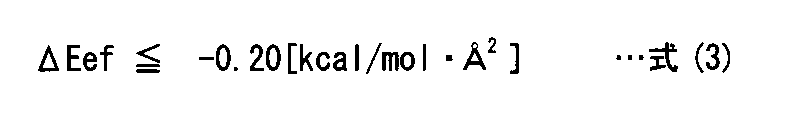

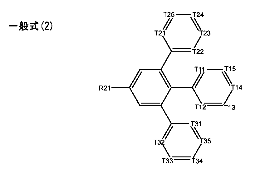
以下に、窒素含有層1aを構成する化合物の具体例(1~134)を示すが、これらに限定されない。尚、ここでは、上記一般式(1)および一般式(2)には含まれない化合物も例示している。また本発明において透明導電層1bに隣接して設けられる窒素含有層1aは、以下に例示される化合物(1~134)のうちから、上述した式(1)または式(2)に当てはまる化合物が選択して用いられる。

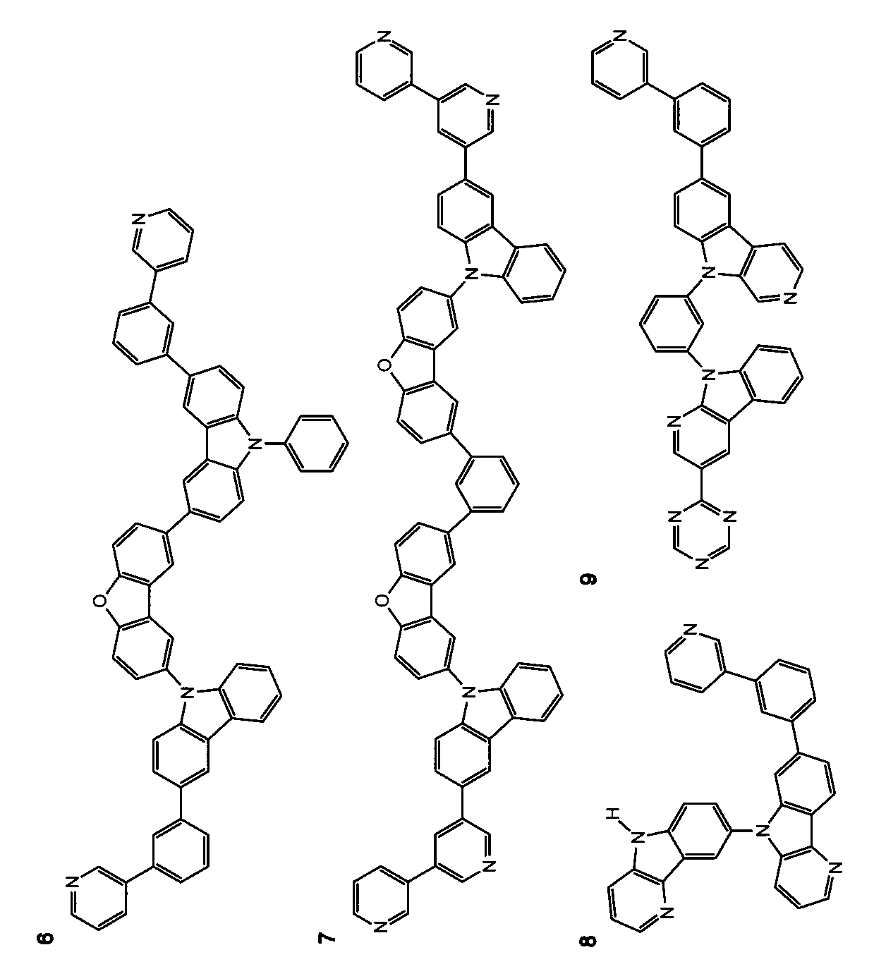


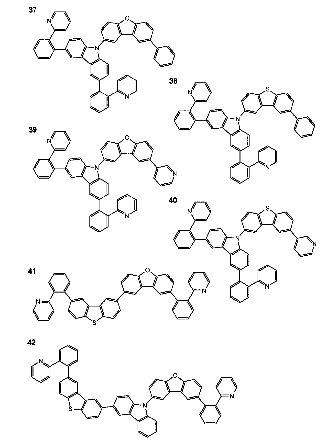
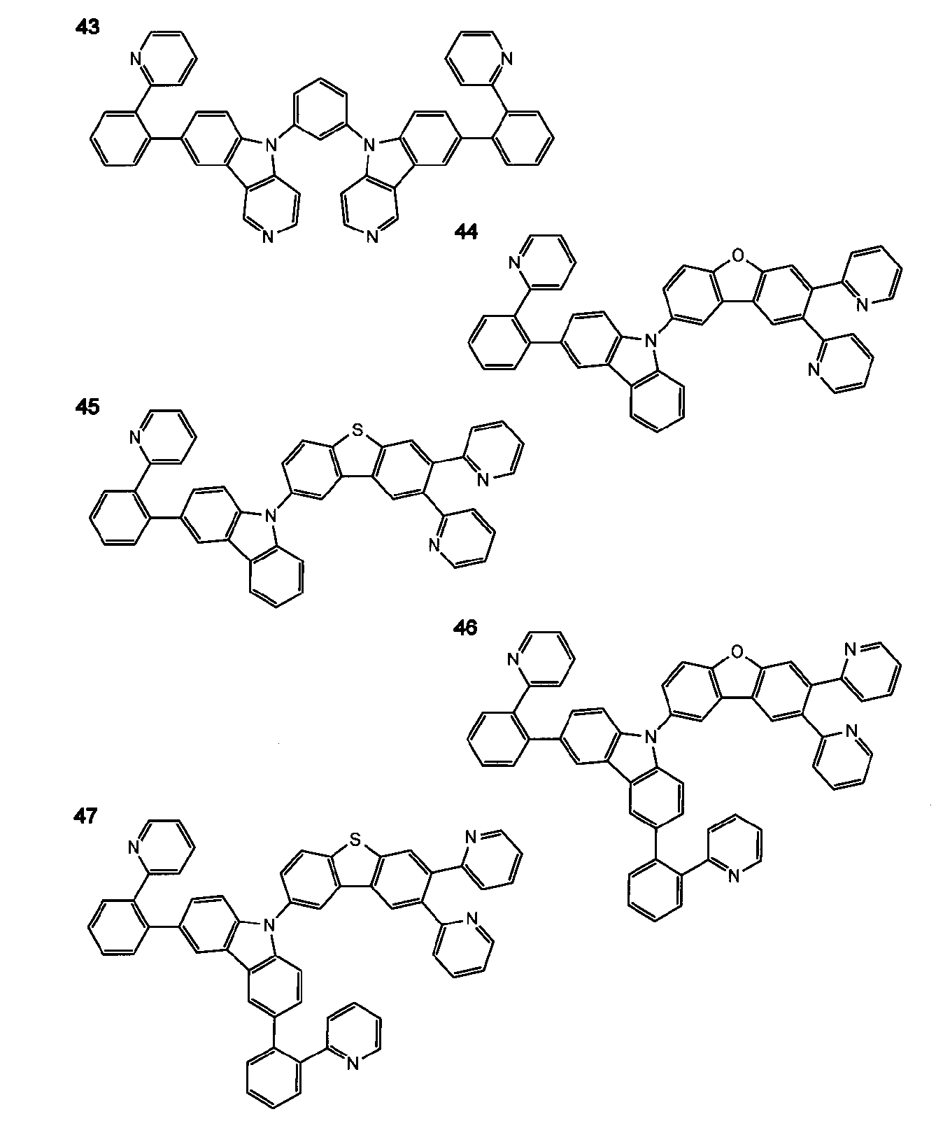
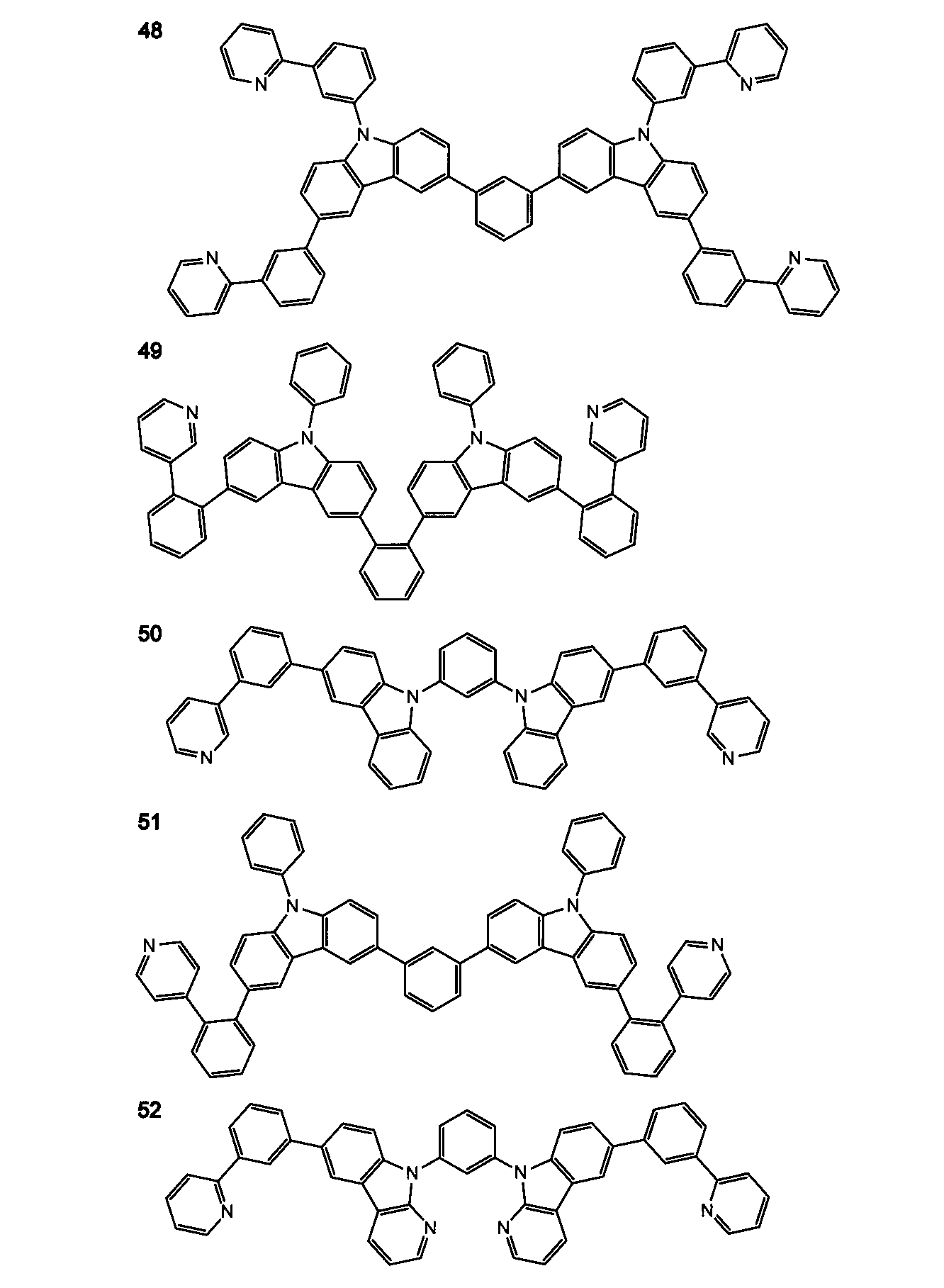


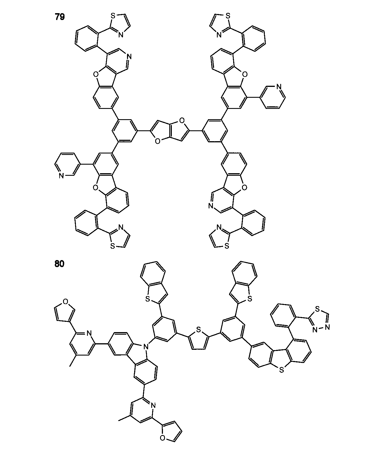
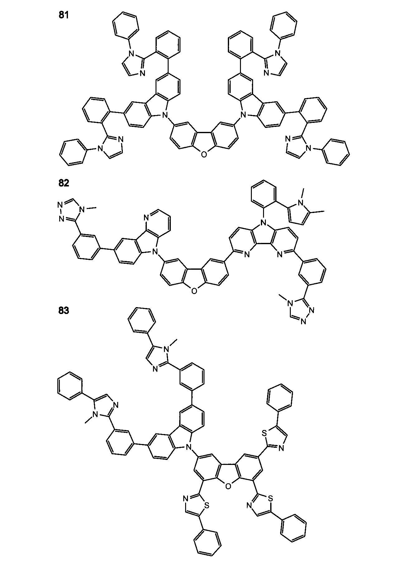

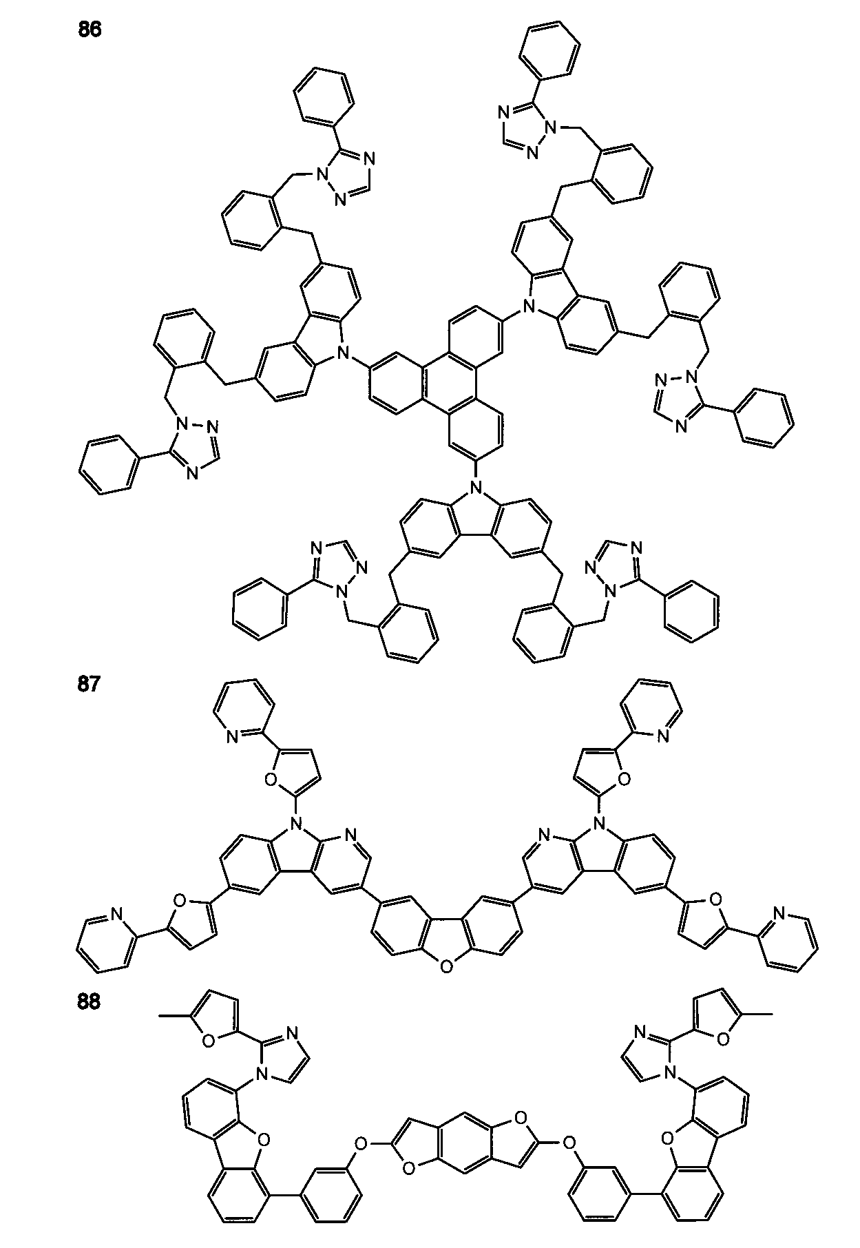

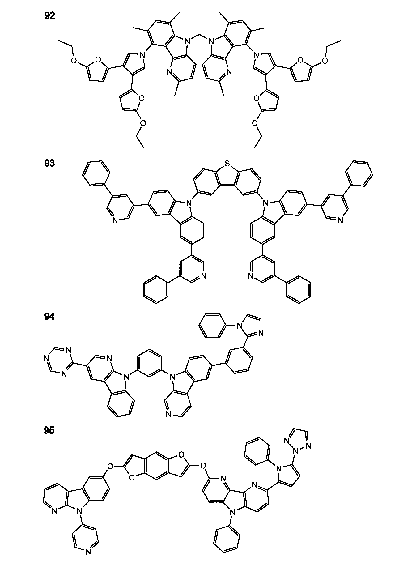


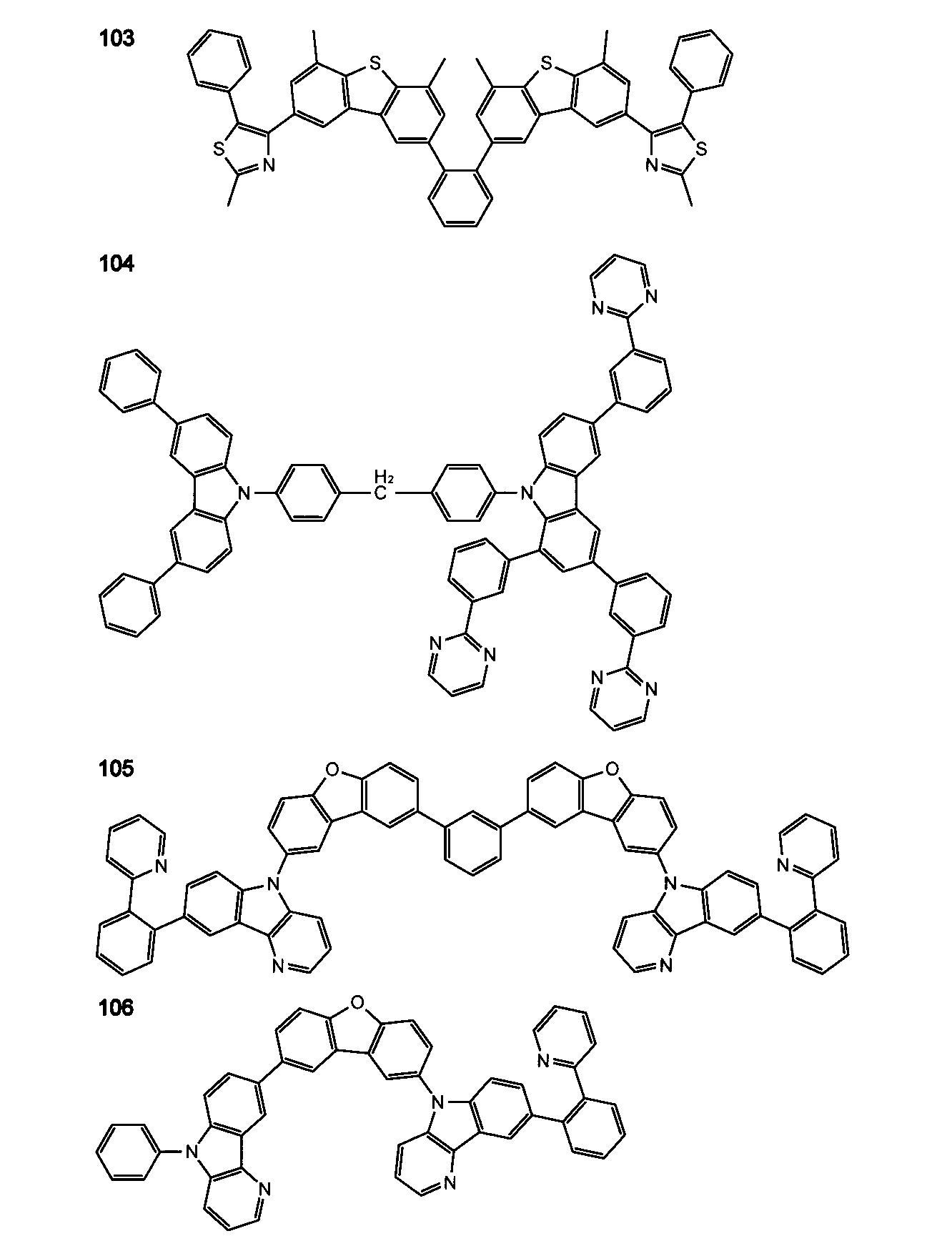


以下に代表的な化合物の合成例として、化合物5の具体的な合成例を示すが、これに限定されない。

窒素雰囲気下、2,8-ジブロモジベンゾフラン(1.0モル)、カルバゾール(2.0モル)、銅粉末(3.0モル)、炭酸カリウム(1.5モル)を、DMAc(ジメチルアセトアミド)300ml中で混合し、130℃で24時間撹拌した。これによって得た反応液を室温まで冷却後、トルエン1Lを加え、蒸留水で3回洗浄し、減圧雰囲気下において洗浄物から溶媒を留去し、その残渣をシリカゲルフラッシュクロマトグラフィー(n-ヘプタン:トルエン=4:1~3:1)にて精製し、中間体1を収率85%で得た。
室温、大気下で中間体1(0.5モル)をDMF(ジメチルホルムアミド)100mlに溶解し、NBS(N-ブロモコハク酸イミド)(2.0モル)を加え、一晩室温で撹拌した。得られた沈殿を濾過し、メタノールで洗浄し、中間体2を収率92%で得た。
窒素雰囲気下、中間体2(0.25モル)、2-フェニルピリジン(1.0モル)、ルテニウム錯体[(η6-C6H6)RuCl2]2(0.05モル)、トリフェニルホスフィン(0.2モル)、炭酸カリウム(12モル)を、NMP(N-メチル-2-ピロリドン)3L中で混合し、140℃で一晩撹拌した。
透明導電層1bは、銀または銀を主成分とした合金を用いて構成された層であって、窒素含有層1aに隣接して成膜された層である。
以上のように構成された透明導電層1bは、窒素原子を含有する化合物を用いて構成された窒素含有層1aに隣接して、銀または銀を主成分とした合金を用いて設けられた構成である。これにより、窒素含有層1aに隣接させて透明導電層1bを成膜する際には、透明導電層1bを構成する銀原子が窒素含有層1aを構成する窒素原子を含んだ化合物と相互作用し、銀原子の窒素含有層1a表面においての拡散距離が減少し、銀の凝集が抑えられる。このため、一般的には核成長型(Volumer-Weber:VW型)での膜成長により島状に孤立し易い銀薄膜が、単層成長型(Frank-van der Merwe:FM型)の膜成長によって成膜されるようになる。したがって、薄い膜厚でありながらも、均一な膜厚の透明導電層1bが得られるようになる。
(2つの発光ユニット間に透明導電層を設けた例)
図2は、上述した透明導電層1bを用いたタンデム構造の有機電界発光素子の第1実施形態を示す断面構成図である。以下にこの図に基づいて有機電界発光素子EL-1の構成を説明する。
図2に示す有機電界発光素子EL-1は、基板11上に設けられており、基板11側から順に、第1電極5、1つ目の発光ユニット3-1、窒素含有層1a、透明導電層1b、2つ目の発光ユニット3-2、および第2電極7をこの順に積層して構成されている。この有機電界発光素子EL-1においては、2つの発光ユニット3-1,3-2間に、先に説明した窒素含有層1aと透明導電層1bとの積層体が挟持されているところが特徴的である。
有機電界発光素子EL-1が設けられる基板11は、例えばガラス、プラスチック等を挙げることができるが、これらに限定されない。また、基板11は透明であっても不透明であってもよい。有機電界発光素子EL-1が、基板11側から光を取り出すボトムエミッション型である場合には、基板11は透明であることが好ましい。好ましく用いられる透明な基板11としては、ガラス、石英、透明樹脂フィルムを挙げることができる。
第1電極5および第2電極7は、何れか一方が発光ユニット3-1,3-2に正孔を供給するための陽極として機能し、何れか他方が発光ユニット3-1,3-2に電子を供給するための陰極として機能する。ここでは一例として、基板11側の第1電極5が陽極、これと逆の第2電極7が陰極であることとする。
窒素含有層1aおよび透明導電層1bは先に説明した構成のものであり、ここでは例えば基板11側から順に、窒素含有層1a、透明導電層1bが配置されている。ここで第1電極5が陽極、第2電極7が陰極である場合、透明導電層1bは、第1電極(陽極)5側の発光ユニット3-1に対して陰極として機能し、一方、第2電極(陰極)7側の発光ユニット3-2に対して陽極として機能する。
発光ユニット3-1,3-2は、全体的な層構造が限定されることはなく、それぞれが個別に一般的な層構造を有していて良い。一例として、陽極側から順に[正孔注入層/正孔輸送層/発光層/電子輸送層/電子注入層]を積層した構成が例示されるが、このうち少なくとも有機材料を用いて構成された発光層を有することが必須である。正孔注入層および正孔輸送層は、正孔輸送/注入層として設けられても良い。電子輸送層および電子注入層は、電子輸送/注入層として設けられても良い。また各発光ユニット3-1,3-2を構成する各層のうち、例えば電子注入層は無機材料で構成されている場合もある。
本発明に用いられる発光層は、発光材料として例えば燐光発光化合物が含有されている。
発光層に含有されるホスト化合物としては、室温(25℃)における燐光発光の燐光量子収率が0.1未満の化合物が好ましい。さらに好ましくは燐光量子収率が0.01未満である。また、発光層に含有される化合物の中で、その層中での体積比が50%以上であることが好ましい。

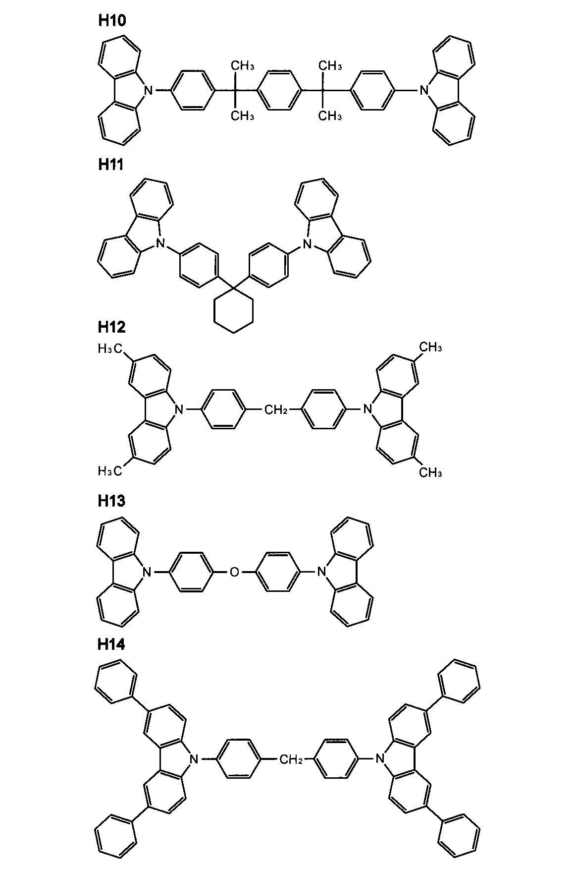


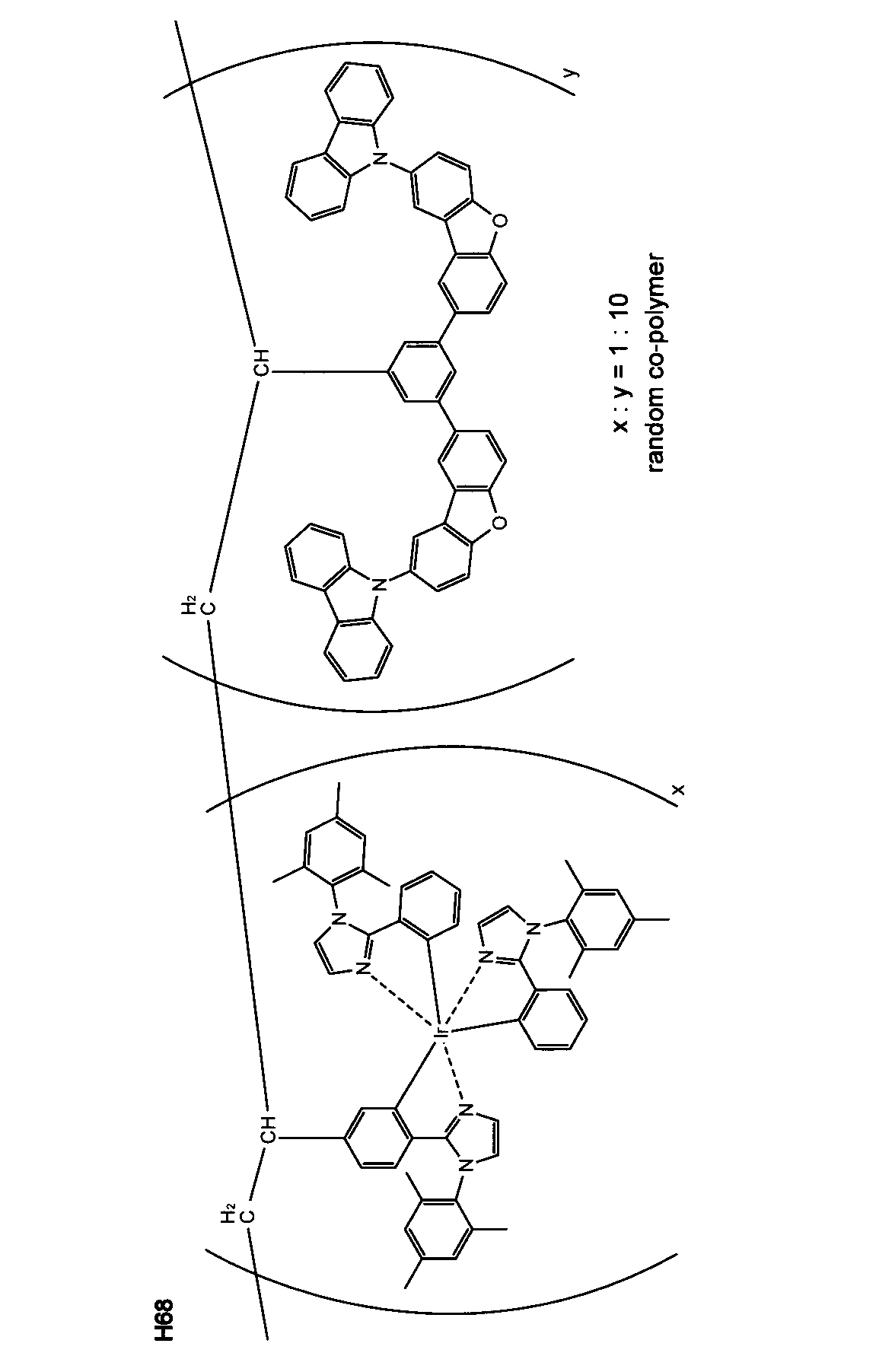


本発明で用いることのできる発光材料としては、燐光発光性化合物(燐光性化合物、燐光発光材料ともいう)が挙げられる。
発光層に含まれる化合物(燐光発光性化合物)は、下記一般式(3)で表される化合物であることが好ましい。

一般式(3)で表される化合物の中でも、下記一般式(4)で表される化合物であることがさらに好ましい。

上記一般式(4)で表される化合物の好ましい態様の一つとして、下記一般式(5)で表される化合物が挙げられる。


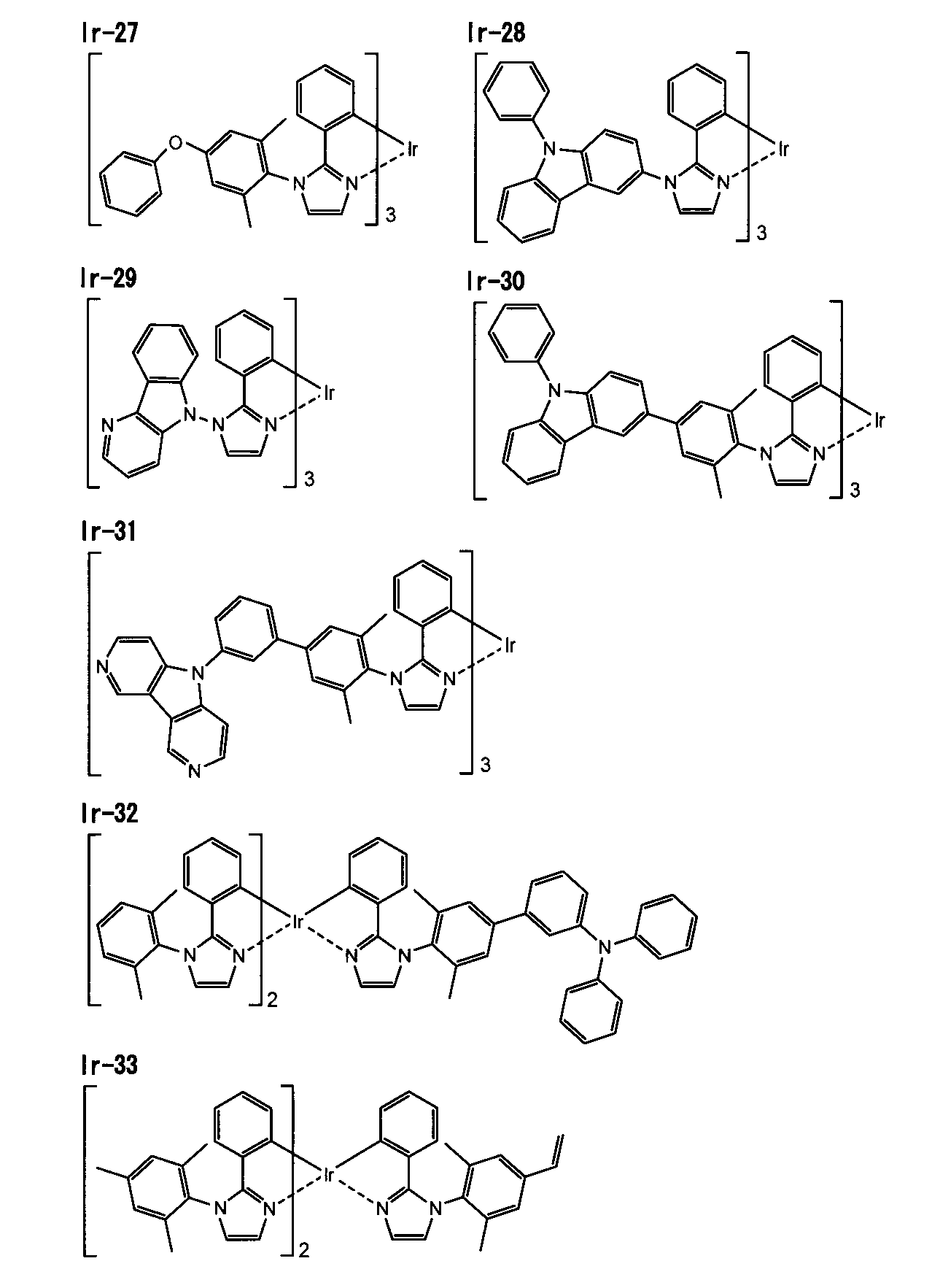

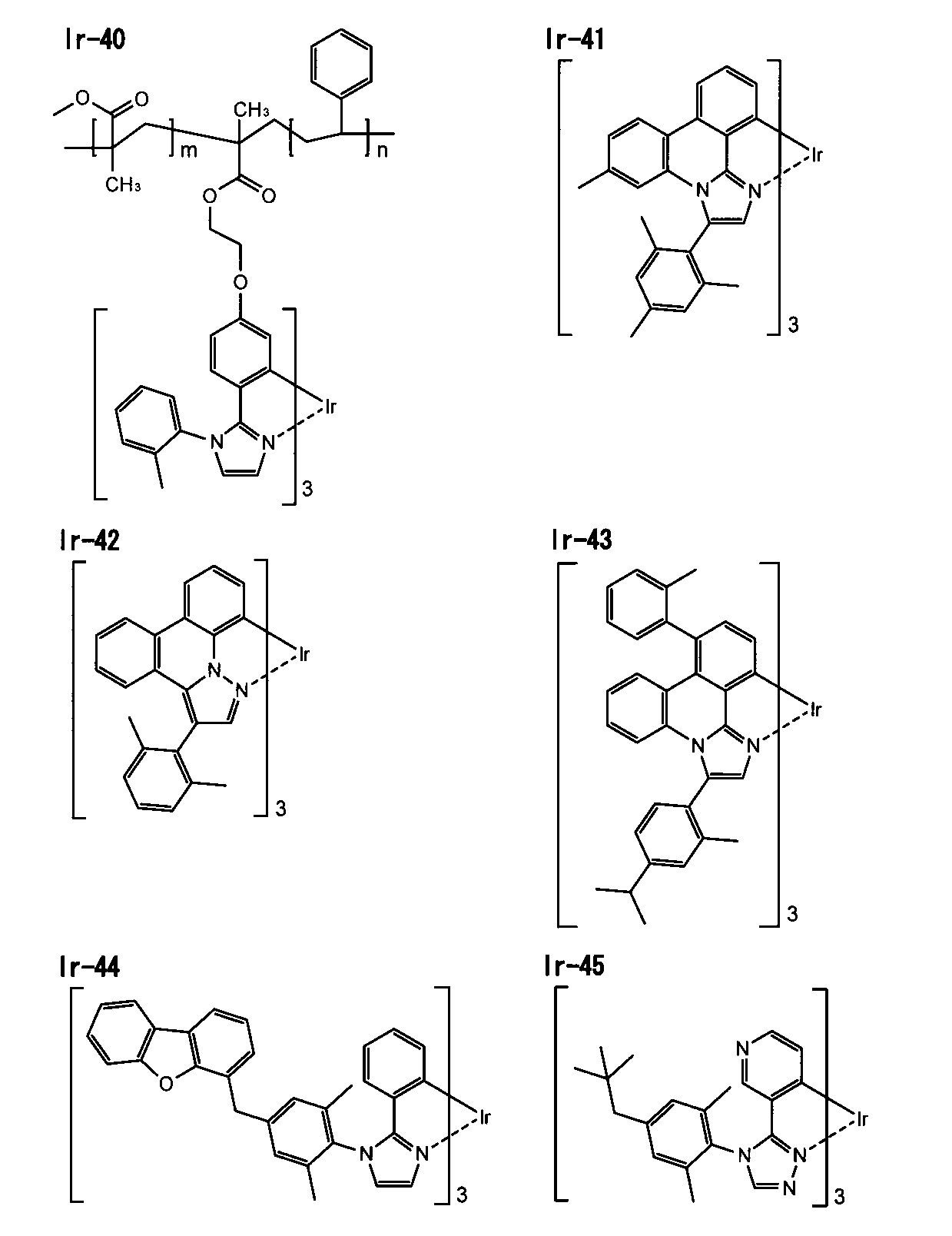

蛍光発光材料としては、クマリン系色素、ピラン系色素、シアニン系色素、クロコニウム系色素、スクアリウム系色素、オキソベンツアントラセン系色素、フルオレセイン系色素、ローダミン系色素、ピリリウム系色素、ペリレン系色素、スチルベン系色素、ポリチオフェン系色素、または希土類錯体系蛍光体等が挙げられる。
注入層とは、駆動電圧低下や発光輝度向上のために電極と発光層の間に設けられる層のことで、「有機EL素子とその工業化最前線(1998年11月30日エヌ・ティー・エス社発行)」の第2編第2章「電極材料」(123~166頁)に詳細に記載されており、正孔注入層と電子注入層とがある。
正孔輸送層は、正孔を輸送する機能を有する正孔輸送材料からなり、広い意味で正孔注入層、電子阻止層も正孔輸送層に含まれる。正孔輸送層は単層または複数層設けることができる。
電子輸送層は、電子を輸送する機能を有する材料からなり、広い意味で電子注入層、正孔阻止層(図示せず)も電子輸送層に含まれる。電子輸送層は単層構造または複数層の積層構造として設けることができる。
一般式(6)中におけるAr1は、下記一般式(A)で表される基を表す。

一般式(A)において、Y3で表される基としては、上記6員の芳香族環から導出される基であることが好ましく、さらに好ましくは、ベンゼン環から導出される基である。
一般式(A)において、Y4で表される基としては、上記6員の芳香族環から導出される基であることが好ましく、さらに好ましくは、窒素原子を環構成原子として含む芳香族複素環から導出される基であり、特に好ましくは、Y4がピリジン環から導出される基であることである。
一般式(A)で表される基の好ましい態様としては、下記一般式(A-1)、(A-2)、(A-3)、または(A-4)のいずれかで表される基が挙げられる。
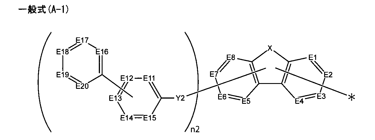


本発明では、上記一般式(6)で表される化合物の中でも、下記一般式(7)で表される化合物が好ましい。この一般式(7)は、窒素含有層1aを構成する化合物として示した一般式(1)を含む。以下、一般式(7)で表される化合物について説明する。

阻止層は、上記の如く有機化合物薄膜の基本構成層の他に、必要に応じて設けられるものである。例えば、特開平11-204258号公報、同11-204359号公報、及び「有機EL素子とその工業化最前線(1998年11月30日エヌ・ティー・エス社発行)」の237頁等に記載されている正孔阻止(ホールブロック)層がある。
以上のような有機電界発光素子EL-1は、光取り出し側となる透明電極(例えばここでは第1電極5)の低抵抗化を図ることを目的とし、第1電極5に接して下記の補助電極が設けられていても良い。また有機材料等を用いて構成された発光ユニット3-1,3-2の劣化を防止することを目的として、基板11上において下記の封止材で封止されている。さらに、基板11との間に有機電界発光素子EL-1および封止材を挟んで、下記の保護膜もしくは保護板を設けても良い。
補助電極は、光透過性を有する電極(例えばここでは第1電極5)の抵抗を下げる目的で設けるものであって、第1電極5に接して設けられる。補助電極を形成する材料は、金、白金、銀、銅、アルミニウム等の抵抗が低い金属が好ましい。これらの金属は光透過性が低いため、光取り出し面からの発光光hの取り出しの影響のない範囲でパターン形成される。このような補助電極の形成方法としては、蒸着法、スパッタリング法、印刷法、インクジェット法、エアロゾルジェット法などが挙げられる。補助電極の線幅は、光を取り出す開口率の観点から50μm以下であることが好ましく、補助電極の厚さは、導電性の観点から1μ以上であることが好ましい。
封止材は、有機電界発光素子EL-1を覆うものであって、板状(フィルム状)の封止部材であって接着剤によって基板11側に固定されるものであっても良く、封止膜であっても良い。ただし、第1電極5および第2電極7の端子部分は、基板11上において発光ユニット3-1,3-2によって互いに絶縁性を保った状態で封止材から露出させた状態で設けられていることとする。
保護膜もしくは保護板は、有機電界発光素子EL-1を機械的に保護するためのものであり、特に封止材が封止膜である場合には、有機電界発光素子EL-1に対する機械的な保護が十分ではないため、このような保護膜もしくは保護板を設けることが好ましい。
先ず基板11上に、蒸着法やスパッタ法などの適宜の成膜法によって、光透過性の第1電極5を陽極として形成する。また、第1電極5の形成前後には、必要に応じて補助電極のパターン形成を行う。
以上説明した有機電界発光素子EL-1は、先に説明した導電性と光透過性とを兼ね備えた透明導電層1bを、発光ユニット3-1,3-2間に挟持させた構成である。このため、発光ユニット3-1,3-2に対して透明導電層1bから十分に電荷を注入して発光効率を確保しつつ、各発光ユニット3-1,3-2で発生させた発光光hの透明導電層1bにおいての吸収を抑えることにより、発光効率の向上を図ることが可能になる。またこれにより、所定輝度を得るための駆動電圧の低減による発光寿命の向上を図ることも可能になる。
図3は、上述した第1実施形態の有機電界発光素子EL-1の変形例1を説明するための断面模式図である。図3に示すように、有機電界発光素子EL-1’は、第1電極5および第2電極7と共に、透明導電層1bにも駆動電圧を印加するようにした構成であり、積層構成については第1実施形態と同様である。
図4は、上述した第1実施形態の有機電界発光素子EL-1の変形例2を説明するための断面模式図である。図4に示すように、有機電界発光素子EL-1”は、第1電極5および第2電極7を同一の極性とし、透明導電層1bに逆極性の駆動電圧を印加するようにした構成であり、2つの発光ユニット3-1,3-2の一方を逆積みとした構成である。他の構成については第1実施形態と同様である。
(発光ユニット間の導電層および第2電極を透明導電層とした例)
図5は、上述した透明導電層1bを用いたタンデム構造の有機電界発光素子の第2実施形態を示す断面構成図である。以下にこの図に基づき、第2実施形態の有機電界発光素子EL-2の特徴的な構成を説明する。尚、第1実施形態と同様の構成要素についての重複する詳細な説明は省略する。
以上説明した有機電界発光素子EL-2は、先に説明した導電性と光透過性とを兼ね備えた透明導電層1b-1,1b-2を、発光ユニット3-1,3-2間に挟持させると共に、第2電極7としても用いた構成である。このため、発光ユニット3-1,3-2に対して2つの透明導電層1b-1,1b-2から十分に電荷を注入して発光効率を確保しつつ、各発光ユニット3-1,3-2で発生させた発光光hの透明導電層1b-1,1b-2においての吸収を抑えて光取り出し効率の向上を図ることが可能になる。またこれにより、所定輝度を得るための電流密度の低減による発光寿命の向上を図ることも可能になる。
また本第2実施形態の構成も、第1実施形態の変形例1の構成と組み合わせることができる。この場合、第1電極5-透明導電層1b-1間に駆動電圧V1を印加し、さらに透明導電層1b-1-第2電極7(透明導電層1b-2)間に駆動電圧V2を印加する構成とする。これにより、第1実施形態の変形例1と同様の効果を得ることができる。
さらに本第2実施形態の構成は、第1実施形態の変形例2の構成と組み合わせることができる。この場合、発光ユニット3-1と、発光ユニット3-2とで、これらを構成する層の積層順を逆にする。このような構成であっても、各発光ユニット3-1,3-2間には、基板11側から順に窒素含有層1a-1、透明導電層1b-1を配置し、発光ユニット3-2上にも基板11側から順に窒素含有層1a-2、透明導電層1b-2を配置する。
(発光ユニット間の導電層および第1電極を透明導電層とした例)
図6は、上述した透明導電層1bを用いたタンデム構造の有機電界発光素子の第3実施形態を示す断面構成図である。以下にこの図に基づき、第3実施形態の有機電界発光素子EL-3の特徴的な構成を説明する。尚、第1実施形態と同様の構成要素についての重複する詳細な説明は省略する。
以上説明した有機電界発光素子EL-3は、先に説明した導電性と光透過性とを兼ね備えた透明導電層1b-1,1b-2を、発光ユニット3-1,3-2間に挟持させると共に、第1電極5としても用いた構成である。このため、発光ユニット3-1,3-2に対して2つの透明導電層1b-1,1b-2から十分に電荷を注入して発光効率を確保しつつ、各発光ユニット3-1,3-2で発生させた発光光hの透明導電層1bにおいての吸収を抑えて光取り出し効率の向上を図ることが可能になる。またこれにより、所定輝度を得るための電流密度の低減による発光寿命の向上を図ることも可能になる。
また本第3実施形態の構成も、第1実施形態の変形例1の構成と組み合わせることができる。この場合、透明導電層1b-1で構成された第1電極5-透明導電層1b-2間に駆動電圧V1を印加し、さらに透明導電層1b-2-第2電極7間に駆動電圧V2を印加する構成とする。これにより、第1実施形態の変形例1と同様の効果を得ることができる。
さらに本第3実施形態の構成は、第1実施形態の変形例2の構成と組み合わせることができる。この場合、発光ユニット3-1と、発光ユニット3-2とで、これらを構成する層の積層順を逆にすることができる。このような構成であっても、基板11上には、基板11側からから順に窒素含有層1a-1、透明導電層1b-1を配置し、各発光ユニット3-1,3-2間にも、基板11側から順に窒素含有層1a-2、透明導電層1b-2を配置する。
(発光ユニット間の導電層および2つの電極を透明導電層とした例)
図7は、上述した透明導電層1bを用いたタンデム構造の有機電界発光素子の第4実施形態を示す断面構成図である。以下にこの図に基づき、第4実施形態の有機電界発光素子EL-4の特徴的な構成を説明する。尚、第1実施形態と同様の構成要素についての重複する詳細な説明は省略する。
以上説明した有機電界発光素子EL-4は、先に説明した導電性と光透過性とを兼ね備えた透明導電層1b-1~1b-3を、発光ユニット3-1,3-2間に挟持させると共に、第1電極5および第2電極7としても用いた構成である。このため、発光ユニット3-1,3-2に対して3つの透明導電層1b-1~1b-3から十分に電荷を注入して発光効率を確保しつつ、各発光ユニット3-1,3-2で発生させた発光光hの透明導電層1b-1~1b-3においての吸収を抑えて光取り出し効率の向上を図ることが可能になる。またこれにより、所定輝度を得るための電流密度の低減による発光寿命の向上を図ることも可能になる。
また本第4実施形態の構成も、第1実施形態の変形例1の構成と組み合わせることができる。この場合、第1電極5(透明導電層1b-1)-透明導電層1b-2間に駆動電圧V1を印加し、さらに透明導電層1b-2-第2電極7(透明導電層1b-3)間に駆動電圧V2を印加する構成とする。これにより、第1実施形態の変形例1と同様の効果を得ることができる。
さらに本第4実施形態の構成は、第1実施形態の変形例2の構成と組み合わせることができる。この場合、発光ユニット3-1と、発光ユニット3-2とで、これらを構成する層の積層順を逆にすることができる。このような構成であっても、各透明導電層1b-1~1b-3の基板11側に隣接させて各窒素含有層1a-1~1a-3を配置する。
(3つ以上の発光ユニット間に透明導電層を設けた例)
図8は、上述した透明導電層1bを用いたタンデム構造の有機電界発光素子の第5実施形態を示す断面構成図である。以下にこの図に基づき第5実施形態の有機電界発光素子EL-5の特徴的な構成を説明する。尚、第1実施形態と同様の構成要素についての重複する詳細な説明は省略する。
以上説明した有機電界発光素子EL-5であっても、先に説明した導電性と光透過性とを兼ね備えた透明導電層1b-1,1b-2を、発光ユニット3-1,3-2間および発光ユニット3-2,3-3間に挟持させた構成である。このため、第1実施形態と同様に、発光ユニット3-1,3-2,3-3に対して透明導電層1b-1,1b-2から十分に電荷を注入して発光効率を確保しつつ、各発光ユニット3-1,3-2,3-3で発生させた発光光hの透明導電層1b-1,1b-2においての吸収を抑えることにより、光取り出し効率の向上を図ることが可能になる。またこれにより、所定輝度を得るための駆動電圧の低減による発光寿命の向上を図ることも可能になる。
また本第5実施形態の構成も、第1実施形態の変形例1の構成と組み合わることができる。この場合、第1電極5および第2電極7と共に、透明導電層1b-1,1b-2にも駆動電圧を印加する構成とする。この際、各発光ユニット3-1,3-2,3-3を挟持して配置される第1電極5、および透明導電層1b-1,1b-2のうちの少なくとも一方、および第2電極7間に、駆動電圧を印加する構成を選択することができる。透明導電層1b-1,1b-2に印加する駆動電圧は、陽極(例えば第1電極5)に印加する電圧と、陰極(例えば第2電極7)に印加する電圧との中間電位であり、陽極側から順に高電位に設定すれば良い。
さらに本第5実施形態の構成は、第1実施形態の変形例2の構成と組み合わせることができる。この場合、各発光ユニット3-1,3-2,3-3を構成する層の積層順を、全て同一方向とせずに、発光ユニット3-1,3-2,3-3のうちの幾つかを逆積みとしても良い。このような構成であっても、各発光ユニット3-1,3-2,3-3間に配置される窒素含有層1a-1,1a-2と透明導電層1b-1,1b-2とは、基板11側から順に窒素含有層1a-1,1a-2と透明導電層1b-1,1b-2となっていることとする。
(3つ以上の発光ユニット間のうちの1箇所に透明導電層を設けた例)
図9は、上述した透明導電層1bを用いたタンデム構造の有機電界発光素子の第6実施形態を示す断面構成図である。以下にこの図に基づき、第6実施形態の有機電界発光素子EL-6の特徴的な構成を説明する。尚、他の実施形態と同様の構成要素についての重複する詳細な説明は省略する。
絶縁性の電荷発生層21は、例えば2種類の物質間で酸化還元反応によってラジカルカチオンとラジカルアニオンからなる電荷移動錯体が形成された層が例示される。この場合、電荷移動錯体中のラジカルカチオン状態(ホール)とラジカルアニオン状態(電子)が、電圧印加時にそれぞれ陰極方向と陽極方向へ移動することにより、前記電荷発生層の陰極側に接する発光ユニットへホールを注入し、電荷発生層の陽極側に接する発光ユニットへ電子を注入する。このような絶縁性の電荷発生層21としては、例えば電子供与性を有する有機化合物(一例としてアリールアミン化合物)と、この有機化合物と酸化還元反応による電荷移動錯体を形成する材料(金属酸化物:5酸化バナジウムや金属ハロゲン化物)との混合層または積層体が例示される(特開2003-272860号公報参照)。
以上説明した有機電界発光素子EL-6であっても、先に説明した導電性と光透過性とを兼ね備えた透明導電層1bを、発光ユニット3-1,3-2間に挟持させた構成である。このため、第1実施形態と同様に、発光ユニット3-1,3-2,3-3に対して透明導電層1bから十分に電荷を注入して発光効率を確保しつつ、各発光ユニット3-1,3-2,3-3で発生させた発光光hの透明導電層1bにおいての吸収を抑えることにより、光取り出し効率の向上を図ることが可能になる。またこれにより、所定輝度を得るための電流密度の低減による発光寿命の向上を図ることも可能になる。
また本第6実施形態の構成も、第1実施形態の変形例1の構成と組み合わせることができる。この場合、第1電極5-透明導電層1b間に駆動電圧V1を印加し、さらに透明導電層1b-第2電極7間に駆動電圧V2を印加する構成とする。これにより、第1実施形態の変形例1と同様の効果を得ることができる。
さらに本第6実施形態の構成は、第1実施形態の変形例2の構成と組み合わせても良い。この場合、透明導電層1bを挟んで配置された発光ユニット3-1と、発光ユニット3-2,3-3とで、これらを構成する層の積層順を逆にすることができる。このような構成であっても、各発光ユニット3-1,3-2,3-3間に配置される窒素含有層1aと透明導電層1bとは、基板11側から窒素含有層1a、透明導電層1bとなっていることとする。
上述した各構成の有機電界発光素子は、上述したように面発光体であるため各種の発光光源として用いることができる。例えば、家庭用照明や車内照明などの照明装置、時計や液晶用のバックライト、看板広告用照明、信号機の光源、光記憶媒体の光源、電子写真複写機の光源、光通信処理機の光源、光センサーの光源等が挙げられるが、これに限定するものではなく、特にカラーフィルターと組み合わせた液晶表示装置のバックライト、照明用光源としての用途に有効に用いることができる。
本発明の照明装置は、上記有機電界発光素子を有する。
また本発明の有機電界発光素子は、複数用いて発光面を大面積化した照明装置としても用いることができる。この場合、透明基板上に有機電界発光素子を設けた複数の発光パネルを、支持基板上に複数配列する(すなわちタイリングする)ことによって発光面を大面積化する。支持基板は、封止材を兼ねるものであっても良く、この支持基板と、発光パネルの透明基板との間に有機電界発光素子を挟持する状態で各発光パネルをタイリングする。支持基板と透明基板との間には接着剤を充填し、これによって有機電界発光素子を封止しても良い。尚、発光パネルの周囲には、第1電極および第2電極の端子を露出させておる。また、導電性の導電層(例えば透明導電層1b)にも駆動電圧を印加する場合であれば、その端子も露出させておく。
以下に説明するように、試料101~112の各透明導電層を、導電性領域の面積が5cm×5cmとなるように作製した。

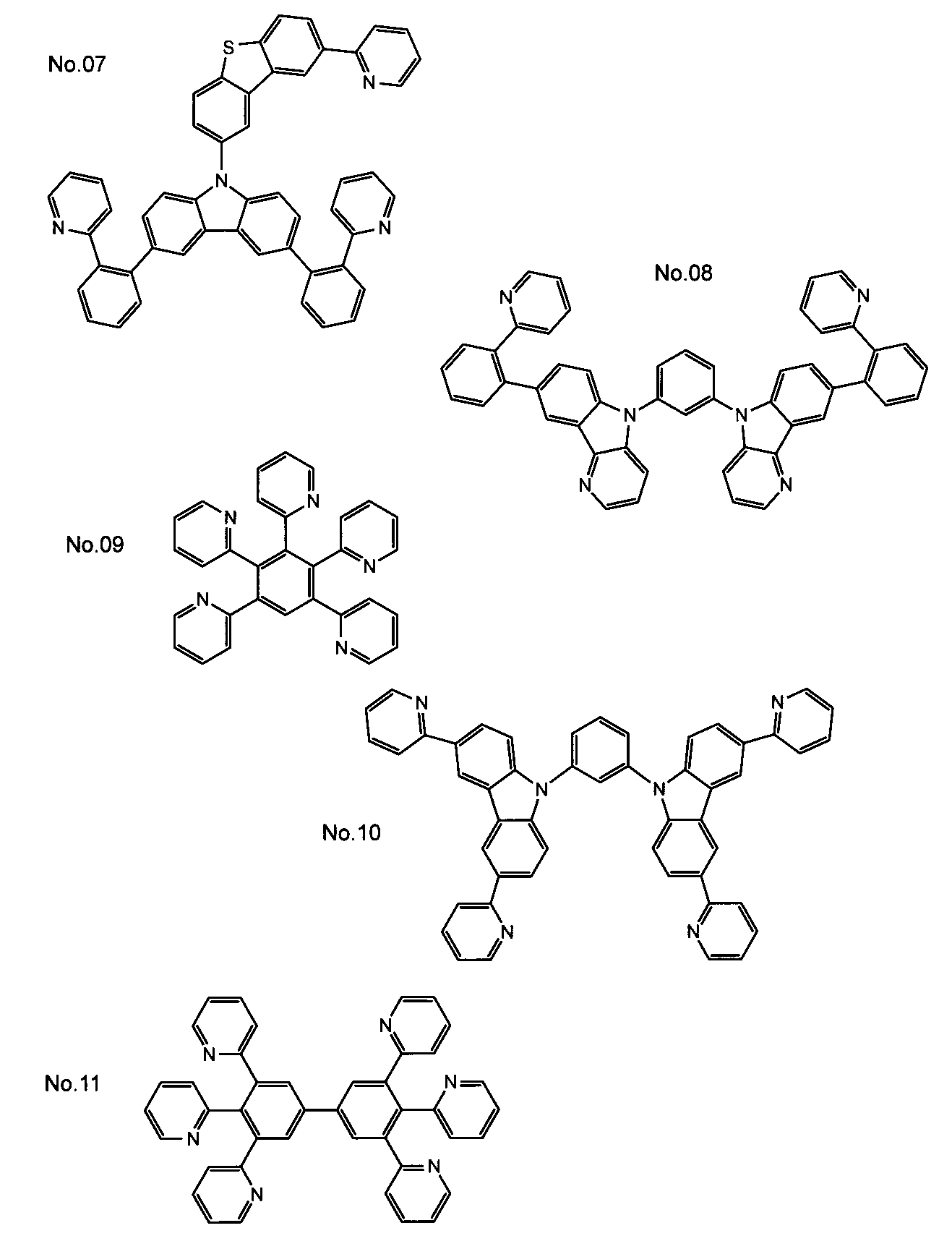

先ず、透明な無アルカリガラス製の基材を、市販の真空蒸着装置の基材ホルダーに固定し、真空蒸着装置の真空槽に取り付けた。またタングステン製の抵抗加熱ボートに銀(Ag)を入れ、当該真空槽内に取り付けた。次に、真空槽を4×10⁻⁴Paまで減圧した後、抵抗加熱ボートを通電して加熱し、蒸着速度0.1nm/秒~0.2nm/秒で、膜厚5nmの銀からなる透明導電層を基材上に形成した。
透明な無アルカリガラス製の基材を市販の真空蒸着装置の基材ホルダーに固定した。また、各透明導電層の作製において、上記各化合物No.01~No.11をタンタル製抵抗加熱ボートに入れた。これらの基板ホルダーと加熱ボートとを真空蒸着装置の第1真空槽に取り付けた。また、タングステン製の抵抗加熱ボートに銀(Ag)を入れ、第2真空槽内に取り付けた。
上記で作製した試料101~112の各透明導電層について、シート抵抗値を測定した。シート抵抗値の測定は、抵抗率計(三菱化学社製MCP-T610)を用い、四探針法定電流印加方式で行った。この結果を上記表1に合わせて示す。
表1から明らかなように、有効作用エネルギーΔEefがΔEef≦-0.1である化合物No.03~No.11を用いた窒素含有層に隣接させた試料104~112の透明導電層は、5nmと極薄膜でありながらも、シート抵抗値の測定が可能であり、単層成長型(Frank-van der Merwe:FM型)の膜成長によってほぼ均一な膜厚で形成されていることが確認された。これに対して、窒素含有層を設けていない単層構造の試料101の透明導電層、窒素を含有しない化合物No.1を用いて下地となる層に隣接させて設けた試料102の透明導電層、およびΔEef>-0.1である化合物No.02を用いた窒素含有層に隣接させた試料103の透明導電層は、シート抵抗の測定が不可能であった。
図11に示すように、試料201~210として、2層タンデム:ボトムエミッション型の有機電界発光素子を作製した。また図12に示すように、比較の試料211,212として、単層構造のボトムエミッション型の有機電界発光素子を作製した。尚、下記表2には、試料201~212の主要部の構成を示した。
図11を参照し、先ず50mm×50mmで厚さ0.7mmの透明なガラス製の基板11上に、厚さ180nmとなる条件でITOをスパッタ法で成膜、パターニングし、ITOで構成された取り出し電極部分を含む面状の第1電極5を形成した。この第1電極5は、陽極として形成した。ITOで構成された第1電極5を設けた基板11を、イソプロピルアルコールで超音波洗浄し、乾燥窒素ガスで乾燥し、UVオゾン洗浄を5分間行った。


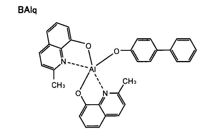

上述した試料201~208の作製において、銀(Ag)で構成された透明導電層1bの形成に換えて、マグネシウム(Mg)と銀(Ag)との共蒸着を行った。この際、Mg:Ag=90:10(原子数%)となるように透明導電層1bを形成した。透明導電層1bの膜厚は8.4nmとした。これ以外は、試料201~208と同様の手順で有機電界発光素子を作製した。尚、窒素含有層1aとしては、化合物Cを用いた。
上述した試料201~208の作製において、銀(Ag)で構成された透明導電層1bの形成に換えて、ITOのスパッタ成膜を行った。この際、発光ユニット3-1に対するダメージを防止するため、成膜速度を0.01nm/secとした。これにより、膜厚120nmのITOからなる透明導電層1bを形成した。これ以外は、試料201~208と同様の手順で有機電界発光素子を作製した。尚、窒素含有層1aとしては、化合物Cを用いた。
図12に示すように、比較として単層構造のボトムエミッション型の有機電界発光素子を作製した。この際、先ず、上述した試料201~208で説明したと同様に、最上層に窒素含有層1aを設けた発光ユニット3-1まで形成した。その後、発光ユニット3が形成された基板11を、真空蒸着装置の第3真空槽内に移送し、第3真空槽内を4×10⁻⁴Paまで減圧した後、第3真空槽内に取り付けられたアルミニウムの入った加熱ボートを通電して加熱した。窒素含有層1a上に、蒸着速度0.2nm/秒で膜厚120nmのアルミニウムからなる第2電極7を形成し、有機電界発光素子を作製した。尚、窒素含有層1aとしては、試料211では化合物Aを用い、試料212では化合物Eを用いた。
試料201~212で作製した有機電界発光素子(発光パネル)について、発光色度を評価した。その結果、試料201~212の全ての素子は、2°視野角正面輝度が1000cd/m2でのCIE1931表色系における色度が、X=0.45±0.02、Y=0.41±0.02の範囲であり、白色であることを確認した。尚、輝度の測定には分光放射輝度計CS-1000(コニカミノルタセンシング製)を用いた。
試料201~212で作製した有機電界発光素子(発光パネル)について、駆動電圧を測定した。駆動電圧の測定においては、上記分光放射輝度計を用い、各有機電界発光素子の基板11側での正面輝度が1000cd/m2となるときの電圧を駆動電圧として測定した。得られた駆動電圧の数値が小さいほど、好ましい結果であることを表わす。この結果を下記表2に合わせて示す。
また試料201~212で作製した有機電界発光素子(発光パネル)について、輝度ムラの評価を行った。輝度ムラの評価においては、各有機電界発光素子に2.5mA/cm2の電流を加え、基板11側の発光面における中心の輝度(中心輝度)と、透明電極1側の給電点に近い端部の輝度(端部輝度)とを測定した。輝度の測定には上記分光放射輝度計を用いた。そして、測定された端部輝度に対する中心輝度を、輝度ムラとして算出した。このため、輝度ムラは、数値が1に近いほど好ましい結果であることを表わす。この結果を下記表2に合わせて示す。
さらに試料201~212で作製した有機電界発光素子(発光パネル)について、外部量子効率(External Quantum Efficiency:EQE)の評価を行った。ここでは、各有機電界発光素子を発光させた際の輝度、および発光スペクトルを、分光放射輝度計CS-1000(コニカミノルタセンシング社製)を用いて測定し、これらの測定値に基づいて輝度換算法により外部量子効率を算出した。ここでは、さらに試料211の有機電界発光素子の値を100とした相対値を算出し、この結果を下記表2に合わせて示す。
さらに試料201~212で作製した有機電界発光素子(発光パネル)について、寿命特性として輝度半減寿命を測定した。輝度半減寿命の測定においては、各有機電界発光素子の基板11側での正面輝度が1000cd/m2となるときの電流を求めた。得られた電流を一定に保ち、経時での輝度の変化を上記分光放射輝度計で測定し、初期輝度に対する輝度が50%になるのに要する時間を、各有機電界発光素子の輝度半減寿命とした。ここでは、試料211の有機電界発光素子の輝度半減寿命を100とした時の相対寿命を算出し、この結果を下記表2に合わせて示す。

表2から明らかなように、積層された発光ユニット3-1,3-2間に、窒素含有層1aに隣接させた状態で銀(Ag)を主成分とした透明導電層1bを配置した試料201~208の有機電界発光素子は、発光ユニット3が単層構造である試料211,212と比較して、外部量子効率(EQE)および寿命の両方が、向上していることが確認された。
図13に示すように、試料301~313として、3層タンデム:両面発光型の有機電界発光素子を作製した。また図14に示すように、比較の試料314,315として、単層構造の両面発光型の有機電界発光素子を作製した。尚、下記表3には、試料301~315の主要部の構成を示した。
図13を参照し、先ず実施例2の試料201~208と同様に、膜厚180nmのITOで構成された第1電極5を陽極として形成し、この上部に正孔注入材料として先に示した構造式HI-2に示す化合物を使用した以外は、試料201~208と同様に第1層目の発光ユニット3-1を形成した。
上述した試料301~308の作製において、銀(Ag)で構成された全3層の透明導電層1b-1~1b-3の形成に換えて、マグネシウム(Mg)と銀(Ag)との共蒸着を行った。この際、試料309ではMg:Ag=45:55(原子数%)、試料310ではMg:Ag=55:45(原子数%)、試料311ではMg:Ag=90:10(原子数%)となるように透明導電層1b-1~1b-3を形成した。膜厚は、3層とも8.4nmとした。これ以外は、試料301~308と同様の手順で有機電界発光素子を作製した。尚、窒素含有層1a-1~1a-3の形成には化合物Eを用いた。
上述した試料301~308の作製において、銀(Ag)で構成された全3層の透明導電層1b-1~1b-3の形成に換えて、ITOのスパッタ成膜を行った。この際、試料312の作製においては成膜速度を0.01nm/secとし、試料313の作製においては成膜速度を0.1nmとした。これにより、膜厚120nmのITOからなる透明導電層1b-1~1b-3を形成した。これ以外は、試料301~308と同様の手順で有機電界発光素子を作製した。尚、窒素含有層1a-1~1a-3の形成には化合物Eを用いた。
図14に示すように、比較として単層構造の両面発光型の有機電界発光素子を作製した。この際、先ず、上述した試料301~308で説明したと同様に、ITOで構成された第1電極5(陽極)上に、発光ユニット3を形成し、さらに透明導電層1bを形成した。透明導電層1bの膜厚は8.4nmとした。この透明導電層1bは、陽極となる第2電極7として形成した。尚、発光ユニット3の最上層を構成する窒素含有層1aとしては、試料314では先に構造式を示した化合物Aを用い、試料315では先に構造式を示した化合物Eを用いた。
試料301~315で作製した有機電界発光素子(発光パネル)について、発光色度を評価した。その結果、試料301~315のうち、試料313以外の全ての素子で発光が確認され、基板11側の2°視野角正面輝度=500cd/m2においてのCIE1931表色系における色度が、X=0.45±0.02、Y=0.41±0.02の範囲であり、白色であることを確認した。尚、輝度の測定には分光放射輝度計CS-1000(コニカミノルタセンシング製)を用いた。
試料301~315で作製した有機電界発光素子(発光パネル)について、実施例2と同様に、駆動電圧、輝度ムラ、外部量子効率(EQE)、および寿命を測定した。ただし、駆動電圧、外部量子効率(EQE)、および寿命については、基板11側での正面輝度を500cd/cm2とした。また、外部量子効率(EQE)および寿命は、試料315の有機電界発光素子の値を100とした時の相対値を算出した。これらの結果を下記表3に合わせて示す。

表3から明らかなように、積層された発光ユニット3-1,3-2,3-3間および上部に、窒素含有層1aに隣接させた状態で銀(Ag)を主成分(50%以上)とした透明導電層1b-1,1b-2,1b-3を配置した試料301~309の有機電界発光素子は、発光ユニット3が単層構造である試料314,315と比較して、外部量子効率(EQE)および寿命の両方が、向上していることが確認された。
図15に示すように、試料401~413として、2層タンデム:トップエミッション型の有機電界発光素子を作製した。また図16に示すように、試料414,415として、単層構造のトップエッション型の有機電界発光素子を作製した。尚、下記表4には、試料401~415の主要部の構成を示した。
図15を参照し、先ず50mm×50mmで厚さ0.7mmの透明なガラス製の基板11を、イソプロピルアルコールで超音波洗浄し、乾燥窒素ガスで乾燥し、UVオゾン洗浄を5分間行った。洗浄した基板11を、真空蒸着装置の第2真空槽内に移送し、第2真空槽内に取り付けられたアルミニウムの入った加熱ボートを通電して加熱した。これにより、蒸着速度0.3nm/秒で膜厚130nmのアルミニウムからなる第1電極5を形成した。この第1電極5は、陽極として用いられる。

上述した試料401~408の作製において、銀(Ag)で構成された全2層の透明導電層1b-1,1b-2の形成に換えて、マグネシウム(Mg)と銀(Ag)との共蒸着を行った。この際、試料409ではMg:Ag=45:55(原子数%)、試料410ではMg:Ag=55:45(原子数%)、試料411ではMg:Ag=90:10(原子数%)となるように透明導電層1b-1,1b-2を形成した。膜厚は、2層とも8.4nmとした。これ以外は、試料401~408と同様の手順で有機電界発光素子を作製した。尚、窒素含有層1a-1,1a-2の形成には化合物Dを用いた。
上述した試料401~408の作製において、銀(Ag)で構成された全2層の透明導電層1b-1~1b-2の形成に換えて、ITOのスパッタ成膜を行った。この際、ITOの成膜速度を0.01nm/secとし、膜厚120nmのITOからなる透明導電層1b-1~1b-2を形成した。これ以外は、試料401~408と同様の手順で有機電界発光素子を作製した。尚、窒素含有層1a-1,1a-2の形成には、試料412では化合物Eを用い、試料413では化合物Cを用いた。
図16に示すように、比較として単層構造のトップエミッション型の有機電界発光素子を作製した。この際、先ず、上述した試料401~408で説明したと同様に、アルミニウムで構成された第1電極5(陽極)上に、発光ユニット3を形成し、さらに透明導電層1bを形成した。尚、発光ユニット3の最上層を構成する窒素含有層1aとしては、試料414では化合物Aを用い、試料415では化合物Fを用いた。また透明導電層1bの膜厚は8.4nmとした。この透明導電層1bは、陰極となる第2電極7として形成した。
試料401~415で作製した有機電界発光素子(発光パネル)について、発光色度を評価した。その結果、試料401~415のうち、試料413以外の全ての素子で発光が確認され、封止基板側(第2電極7側)からの2°視野角正面輝度=400cd/m2でのCIE1931表色系における色度が、X=0.45±0.02、Y=0.41±0.02の範囲であり、白色であることを確認した。尚、輝度の測定には分光放射輝度計CS-1000(コニカミノルタセンシング製)を用いた。
試料401~415で作製した有機電界発光素子(発光パネル)について、実施例2と同様に、駆動電圧、輝度ムラ、外部量子効率(EQE)、および寿命を測定した。ただし、駆動電圧、外部量子効率(EQE)、および寿命については、基板11と逆の第2電極7側での正面輝度を400cd/cm2とした。また、外部量子効率(EQE)および寿命は、試料414の有機電界発光素子の値を100とした時の相対値を算出した。これらの結果を下記表4に合わせて示す。

表4から明らかなように、積層された発光ユニット3-1,3-2間および上部に、窒素含有層1aに隣接させた状態で銀(Ag)を主成分(50%以上)とした透明導電層1b-1,1b-2を配置した試料402~409の有機電界発光素子は、発光ユニット3が単層構造である試料414,415と比較して、外部量子効率(EQE)および寿命の両方ともが1.4倍以上向上していることが確認された。
図17に示すように、試料501~511として、3色・3層タンデム:両面発光型の有機電界発光素子を作製した。尚、下記表5には、試料501~511の主要部の構成を示した。
図17を参照し、先ず実施例2の試料201~208と同様に、膜厚180nmのITOで構成された第1電極5を陽極として形成し、これを洗浄した。
上述した試料501~508の作製において、銀(Ag)で構成された全3層の透明導電層1b-1~1b-3の形成に換えて、マグネシウム(Mg)と銀(Ag)との共蒸着を行った。この際、試料509ではMg:Ag=45:55(原子数%)、試料510ではMg:Ag=55:45(原子数%)、試料511ではMg:Ag=90:10(原子数%)となるように透明導電層1b-1~1b-3を形成した。膜厚は、第1層目および第2層目の透明導電層1b-1,1b-2を6.0nmとし、第3層目の透明導電層1b-3を8.4nmとした。これ以外は、試料501と同様の手順で有機電界発光素子を作製した。尚、各発光ユニット3-1~3-3の最上層を構成する窒素含有層1a-1~1a-3としては、化合物Eを用いた。
試料501~511で作製した有機電界発光素子(発光パネル)について、発光色度を評価した。この結果を下記表5に示す。

図18に示すように、試料601~606として、逆積み・2層タンデム:両面発光型の有機電界発光素子を作製した。尚、下記表6には、試料601~606の主要部の構成を示した。
図18を参照し、先ず実施例2の試料201~208と同様に、ITOで構成された第1電極5を陽極として形成し、これを洗浄した。
試料601~606で作製した有機電界発光素子(発光パネル)について、第1電極5側の輝度、第2電極側の輝度、および発光色を評価した。この際、各有機電界発光素子に対して下記表6に示すように、第1電極5(陽極)-透明導電層1b-1(陰極)間に駆動電圧V1を印加し、透明導電層1b-1(陰極)-透明導電層1b-2(第2電極7:陽極)間に駆動電圧V2に印加して発光を得た。第1電極5側の輝度、第2電極側の輝度は、2°視野角正面輝度を測定し、試料601の第1電極5側の正面輝度を100とした相対値を算出した。また、発光色は目視による色調で判断した。尚、輝度の測定には分光放射輝度計CS-1000(コニカミノルタセンシング製)を用いた。以上の結果を下記表6に示す。

表6から明らかなように、本発明構成の窒素含有層1a-1に隣接する透明導電層1b-1を有するタンデム構造の有機電界発光素子は、それぞれを構成する各層の積層順を逆とした発光ユニット3-1,3-2を用いた場合であっても、発光が得られることが確認された。
Claims (6)
- 一対の電極と、
有機材料を用いて構成された発光層を有して前記電極間に重ねて配置された複数の発光ユニットと、
前記発光ユニット間に配置された導電層とを備え、
前記電極および前記導電層のうちの少なくとも1つは、
銀または銀を主成分とした合金を用いた透明導電層として構成されると共に、窒素原子を含有する化合物を用いて構成された窒素含有層に隣接して配置されている
有機電界発光素子。 - 前記化合物は、下記式(1)で表される銀との有効作用エネルギーΔEefが下記式(2)を満たす
請求項1に記載の有機電界発光素子。
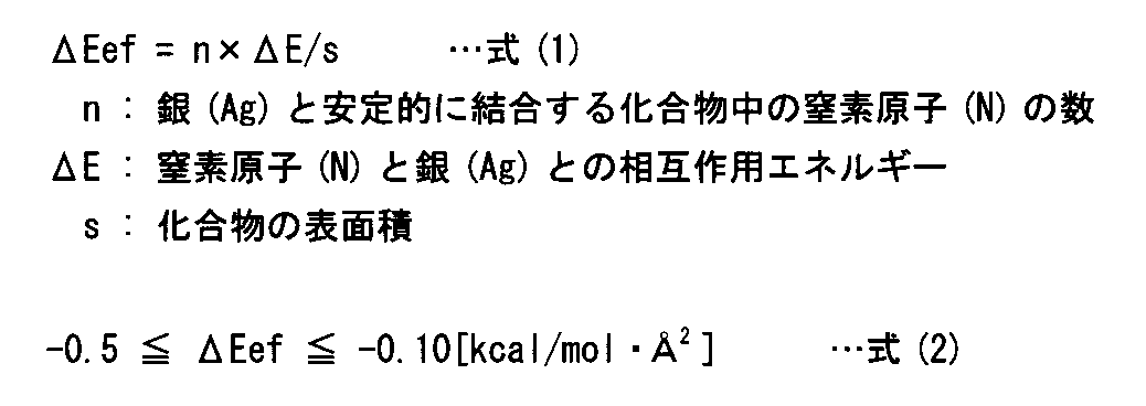
- 前記化合物は、下記一般式(1)で表される化合物を含む
請求項1または2に記載の有機電界発光素子。

E51~E66、E71~E88は、各々-C(R3)=または-N=を表し、R3は水素原子または置換基を表す。
またE71~E79の少なくとも1つおよびE80~E88の少なくとも1つは-N=を表す。n3およびn4は0~4の整数を表すが、n3+n4は2以上の整数である。〕 - 前記化合物は、下記一般式(2)で表される化合物を含む
請求項1または2に記載の有機電界発光素子。

R21は置換基を表し、
T11,T12、T21~T25、T31~T35は、各々-C(R22)=または-N=を表し、
T13~T15は、各々-C(R22)=を表し、
前記R22は、水素原子(H)または置換基を表し、
T11およびT12のうち少なくとも1つは-N=であり、
T21~T25のうち少なくとも1つは-N=であり、
T31~T35のうち少なくとも1つは-N=である。〕 - 前記一対の電極のみに電圧を印加して駆動される
請求項1~4の何れかに記載の有機電界発光素子。 - 前記一対の電極および前記導電層に電圧を印加して駆動される
請求項1~4の何れかに記載の有機電界発光素子。
Priority Applications (3)
| Application Number | Priority Date | Filing Date | Title |
|---|---|---|---|
| US14/385,601 US20150041788A1 (en) | 2012-03-21 | 2013-03-11 | Organic electroluminescence element |
| EP13764183.3A EP2830397A4 (en) | 2012-03-21 | 2013-03-11 | ORGANIC ELECTROLUMINESCENT ELEMENT |
| JP2014506141A JP6137170B2 (ja) | 2012-03-21 | 2013-03-11 | 有機電界発光素子 |
Applications Claiming Priority (2)
| Application Number | Priority Date | Filing Date | Title |
|---|---|---|---|
| JP2012064229 | 2012-03-21 | ||
| JP2012-064229 | 2012-03-21 |
Publications (1)
| Publication Number | Publication Date |
|---|---|
| WO2013141057A1 true WO2013141057A1 (ja) | 2013-09-26 |
Family
ID=49222517
Family Applications (1)
| Application Number | Title | Priority Date | Filing Date |
|---|---|---|---|
| PCT/JP2013/056616 WO2013141057A1 (ja) | 2012-03-21 | 2013-03-11 | 有機電界発光素子 |
Country Status (4)
| Country | Link |
|---|---|
| US (1) | US20150041788A1 (ja) |
| EP (1) | EP2830397A4 (ja) |
| JP (1) | JP6137170B2 (ja) |
| WO (1) | WO2013141057A1 (ja) |
Cited By (5)
| Publication number | Priority date | Publication date | Assignee | Title |
|---|---|---|---|---|
| WO2016063870A1 (ja) * | 2014-10-21 | 2016-04-28 | コニカミノルタ株式会社 | 表示装置 |
| WO2016063871A1 (ja) * | 2014-10-21 | 2016-04-28 | コニカミノルタ株式会社 | 表示装置 |
| WO2016072246A1 (ja) * | 2014-11-04 | 2016-05-12 | コニカミノルタ株式会社 | 有機エレクトロルミネッセンス素子 |
| WO2016136397A1 (ja) * | 2015-02-27 | 2016-09-01 | コニカミノルタ株式会社 | 透明電極及び電子デバイス |
| US9818962B2 (en) | 2014-01-31 | 2017-11-14 | Konica Minolta, Inc. | Organic electroluminescent element and method for manufacturing same |
Families Citing this family (3)
| Publication number | Priority date | Publication date | Assignee | Title |
|---|---|---|---|---|
| JP6277581B2 (ja) * | 2012-12-17 | 2018-02-14 | コニカミノルタ株式会社 | 有機エレクトロルミネッセンス素子 |
| CN104966789A (zh) * | 2015-06-30 | 2015-10-07 | 深圳市华星光电技术有限公司 | 一种电荷连接层及其制造方法、叠层oled器件 |
| US11167375B2 (en) | 2018-08-10 | 2021-11-09 | The Research Foundation For The State University Of New York | Additive manufacturing processes and additively manufactured products |
Citations (60)
| Publication number | Priority date | Publication date | Assignee | Title |
|---|---|---|---|---|
| US5061569A (en) | 1990-07-26 | 1991-10-29 | Eastman Kodak Company | Electroluminescent device with organic electroluminescent medium |
| JPH04297076A (ja) | 1991-01-31 | 1992-10-21 | Toshiba Corp | 有機el素子 |
| JPH04308688A (ja) | 1991-04-08 | 1992-10-30 | Pioneer Electron Corp | 有機エレクトロルミネッセンス素子 |
| JPH06325871A (ja) | 1993-05-18 | 1994-11-25 | Mitsubishi Kasei Corp | 有機電界発光素子 |
| JPH08288069A (ja) | 1995-04-07 | 1996-11-01 | Sanyo Electric Co Ltd | 有機エレクトロルミネッセンス素子 |
| JPH0917574A (ja) | 1995-04-27 | 1997-01-17 | Pioneer Electron Corp | 有機エレクトロルミネッセンス素子 |
| JPH0945479A (ja) | 1995-07-27 | 1997-02-14 | Hewlett Packard Co <Hp> | 有機エレクトロルミネセンス装置及び有機エレクトロルミネセンス装置の製造方法 |
| JPH09260062A (ja) | 1996-03-25 | 1997-10-03 | Tdk Corp | 有機エレクトロルミネセンス素子 |
| JPH1074586A (ja) | 1996-07-29 | 1998-03-17 | Eastman Kodak Co | エレクトロルミネセンスデバイスで用いられる二層電子注入電極 |
| JPH10270172A (ja) | 1997-01-27 | 1998-10-09 | Junji Kido | 有機エレクトロルミネッセント素子 |
| JPH11204359A (ja) | 1998-01-14 | 1999-07-30 | Tokin Corp | 圧粉磁芯の製造方法と製造装置 |
| JPH11204258A (ja) | 1998-01-09 | 1999-07-30 | Sony Corp | 電界発光素子及びその製造方法 |
| JPH11251067A (ja) | 1998-03-02 | 1999-09-17 | Junji Kido | 有機エレクトロルミネッセント素子 |
| JPH11329749A (ja) * | 1998-05-12 | 1999-11-30 | Tdk Corp | 有機el表示装置及びその製造方法 |
| JP2000196140A (ja) | 1998-12-28 | 2000-07-14 | Sharp Corp | 有機エレクトロルミネッセンス素子とその製造法 |
| JP2001102175A (ja) | 1999-09-29 | 2001-04-13 | Junji Kido | 有機エレクトロルミネッセント素子、有機エレクトロルミネッセント素子群及びその発光スペクトルの制御方法 |
| JP2001257076A (ja) | 2000-03-13 | 2001-09-21 | Tdk Corp | 有機el素子 |
| JP2001313179A (ja) | 2000-05-01 | 2001-11-09 | Mitsubishi Chemicals Corp | 有機電界発光素子 |
| JP2001357977A (ja) | 2000-06-12 | 2001-12-26 | Fuji Photo Film Co Ltd | 有機電界発光素子 |
| US6337492B1 (en) | 1997-07-11 | 2002-01-08 | Emagin Corporation | Serially-connected organic light emitting diode stack having conductors sandwiching each light emitting layer |
| JP2002008860A (ja) | 2000-04-18 | 2002-01-11 | Mitsubishi Chemicals Corp | 有機電界発光素子 |
| JP2002015871A (ja) | 2000-04-27 | 2002-01-18 | Toray Ind Inc | 発光素子 |
| JP2002043056A (ja) | 2000-07-19 | 2002-02-08 | Canon Inc | 発光素子 |
| JP2002075645A (ja) | 2000-08-29 | 2002-03-15 | Semiconductor Energy Lab Co Ltd | 発光装置 |
| JP2002105445A (ja) | 2000-09-29 | 2002-04-10 | Fuji Photo Film Co Ltd | 有機発光素子材料及びそれを用いた有機発光素子 |
| JP2002141173A (ja) | 2000-08-22 | 2002-05-17 | Semiconductor Energy Lab Co Ltd | 発光装置 |
| JP2002203683A (ja) | 2000-10-30 | 2002-07-19 | Toyota Central Res & Dev Lab Inc | 有機電界発光素子 |
| JP2002231453A (ja) | 2000-11-30 | 2002-08-16 | Mitsubishi Chemicals Corp | 有機電界発光素子 |
| JP2002234888A (ja) | 2001-02-09 | 2002-08-23 | Mitsui Chemicals Inc | アミン化合物および該化合物を含有する有機電界発光素子 |
| JP2002255934A (ja) | 2000-12-25 | 2002-09-11 | Fuji Photo Film Co Ltd | 新規化合物、その重合体、それらを利用した発光素子材料およびその発光素子 |
| JP2002260861A (ja) | 2001-01-02 | 2002-09-13 | Eastman Kodak Co | 有機発光デバイス |
| JP2002280183A (ja) | 2000-12-28 | 2002-09-27 | Toshiba Corp | 有機el素子および表示装置 |
| JP2002299060A (ja) | 2001-03-30 | 2002-10-11 | Fuji Photo Film Co Ltd | 有機発光素子 |
| JP2002305083A (ja) | 2001-04-04 | 2002-10-18 | Mitsubishi Chemicals Corp | 有機電界発光素子 |
| JP2002305084A (ja) | 2000-12-25 | 2002-10-18 | Fuji Photo Film Co Ltd | 新規インドール誘導体およびそれを利用した発光素子 |
| JP2002302516A (ja) | 2001-04-03 | 2002-10-18 | Fuji Photo Film Co Ltd | 新規ポリマーおよびそれを用いた発光素子 |
| JP2002308837A (ja) | 2001-04-05 | 2002-10-23 | Fuji Photo Film Co Ltd | 新規化合物、およびそれを用いた発光素子 |
| JP2002308855A (ja) | 2001-04-05 | 2002-10-23 | Fuji Photo Film Co Ltd | 新規化合物、およびそれを用いた発光素子 |
| JP2002319491A (ja) | 2000-08-24 | 2002-10-31 | Fuji Photo Film Co Ltd | 発光素子及び新規重合体子 |
| JP2002334789A (ja) | 2001-03-09 | 2002-11-22 | Sony Corp | 有機電界発光素子 |
| JP2002334786A (ja) | 2001-03-09 | 2002-11-22 | Sony Corp | 有機電界発光素子 |
| JP2002334787A (ja) | 2001-03-09 | 2002-11-22 | Sony Corp | 有機電界発光素子 |
| JP2002334788A (ja) | 2001-03-09 | 2002-11-22 | Sony Corp | 有機電界発光素子 |
| JP2002338579A (ja) | 2001-03-16 | 2002-11-27 | Fuji Photo Film Co Ltd | ヘテロ環化合物及びそれを用いた発光素子 |
| JP2002343568A (ja) | 2001-05-10 | 2002-11-29 | Sony Corp | 有機電界発光素子 |
| JP2002352957A (ja) | 2001-05-23 | 2002-12-06 | Honda Motor Co Ltd | 有機エレクトロルミネッセンス素子 |
| JP2002363227A (ja) | 2001-04-03 | 2002-12-18 | Fuji Photo Film Co Ltd | 新規ポリマーおよびそれを用いた発光素子 |
| JP2003003165A (ja) | 2001-06-25 | 2003-01-08 | Showa Denko Kk | 有機発光素子および発光材料 |
| JP2003027048A (ja) | 2001-07-11 | 2003-01-29 | Fuji Photo Film Co Ltd | 発光素子 |
| JP2003272860A (ja) | 2002-03-26 | 2003-09-26 | Junji Kido | 有機エレクトロルミネッセント素子 |
| JP3496681B2 (ja) | 1994-12-13 | 2004-02-16 | ザ、トラスティーズ オブ プリンストン ユニバーシティ | 多色オーガニック発光素子 |
| JP2004068143A (ja) | 2002-06-10 | 2004-03-04 | Konica Minolta Holdings Inc | 薄膜形成方法並びに該薄膜形成方法により薄膜が形成された基材 |
| JP2005100921A (ja) * | 2003-08-22 | 2005-04-14 | Sony Corp | 有機el素子および表示装置 |
| JP2005135600A (ja) | 2003-10-28 | 2005-05-26 | Idemitsu Kosan Co Ltd | 有機エレクトロルミネッセンス発光素子 |
| JP2005340187A (ja) | 2004-04-28 | 2005-12-08 | Semiconductor Energy Lab Co Ltd | 発光素子およびその作製方法、並びに前記発光素子を用いた発光装置 |
| JP2006332048A (ja) | 2005-05-20 | 2006-12-07 | Lg Phillips Lcd Co Ltd | 積層型oled用中間電極 |
| WO2009054253A1 (ja) * | 2007-10-26 | 2009-04-30 | Konica Minolta Holdings, Inc. | 有機エレクトロルミネッセンス素子、表示装置及び照明装置 |
| JP2009224274A (ja) * | 2008-03-18 | 2009-10-01 | Panasonic Electric Works Co Ltd | 有機エレクトロルミネッセンス素子及び照明装置 |
| JP2010251675A (ja) * | 2008-05-13 | 2010-11-04 | Konica Minolta Holdings Inc | 有機エレクトロルミネッセンス素子、表示装置及び照明装置 |
| JP2011077028A (ja) * | 2009-09-04 | 2011-04-14 | Hitachi Displays Ltd | 有機el表示装置 |
Family Cites Families (5)
| Publication number | Priority date | Publication date | Assignee | Title |
|---|---|---|---|---|
| US5703436A (en) * | 1994-12-13 | 1997-12-30 | The Trustees Of Princeton University | Transparent contacts for organic devices |
| KR100847219B1 (ko) * | 2006-03-07 | 2008-07-17 | 주식회사 엘지화학 | 유기발광소자 및 그 제조방법 |
| KR20080082134A (ko) * | 2007-03-07 | 2008-09-11 | 삼성에스디아이 주식회사 | 유기전계발광표시장치 및 그 제조방법 |
| US20160055937A1 (en) * | 2012-07-11 | 2016-02-25 | Konica Minolta, Inc. | Transparent electrode for touch panel, touch panel, and display device |
| US9871220B2 (en) * | 2012-11-28 | 2018-01-16 | Konica Minolta, Inc. | Transparent electrode, and electronic device |
-
2013
- 2013-03-11 EP EP13764183.3A patent/EP2830397A4/en not_active Withdrawn
- 2013-03-11 JP JP2014506141A patent/JP6137170B2/ja active Active
- 2013-03-11 WO PCT/JP2013/056616 patent/WO2013141057A1/ja active Application Filing
- 2013-03-11 US US14/385,601 patent/US20150041788A1/en not_active Abandoned
Patent Citations (60)
| Publication number | Priority date | Publication date | Assignee | Title |
|---|---|---|---|---|
| US5061569A (en) | 1990-07-26 | 1991-10-29 | Eastman Kodak Company | Electroluminescent device with organic electroluminescent medium |
| JPH04297076A (ja) | 1991-01-31 | 1992-10-21 | Toshiba Corp | 有機el素子 |
| JPH04308688A (ja) | 1991-04-08 | 1992-10-30 | Pioneer Electron Corp | 有機エレクトロルミネッセンス素子 |
| JPH06325871A (ja) | 1993-05-18 | 1994-11-25 | Mitsubishi Kasei Corp | 有機電界発光素子 |
| JP3496681B2 (ja) | 1994-12-13 | 2004-02-16 | ザ、トラスティーズ オブ プリンストン ユニバーシティ | 多色オーガニック発光素子 |
| JPH08288069A (ja) | 1995-04-07 | 1996-11-01 | Sanyo Electric Co Ltd | 有機エレクトロルミネッセンス素子 |
| JPH0917574A (ja) | 1995-04-27 | 1997-01-17 | Pioneer Electron Corp | 有機エレクトロルミネッセンス素子 |
| JPH0945479A (ja) | 1995-07-27 | 1997-02-14 | Hewlett Packard Co <Hp> | 有機エレクトロルミネセンス装置及び有機エレクトロルミネセンス装置の製造方法 |
| JPH09260062A (ja) | 1996-03-25 | 1997-10-03 | Tdk Corp | 有機エレクトロルミネセンス素子 |
| JPH1074586A (ja) | 1996-07-29 | 1998-03-17 | Eastman Kodak Co | エレクトロルミネセンスデバイスで用いられる二層電子注入電極 |
| JPH10270172A (ja) | 1997-01-27 | 1998-10-09 | Junji Kido | 有機エレクトロルミネッセント素子 |
| US6337492B1 (en) | 1997-07-11 | 2002-01-08 | Emagin Corporation | Serially-connected organic light emitting diode stack having conductors sandwiching each light emitting layer |
| JPH11204258A (ja) | 1998-01-09 | 1999-07-30 | Sony Corp | 電界発光素子及びその製造方法 |
| JPH11204359A (ja) | 1998-01-14 | 1999-07-30 | Tokin Corp | 圧粉磁芯の製造方法と製造装置 |
| JPH11251067A (ja) | 1998-03-02 | 1999-09-17 | Junji Kido | 有機エレクトロルミネッセント素子 |
| JPH11329749A (ja) * | 1998-05-12 | 1999-11-30 | Tdk Corp | 有機el表示装置及びその製造方法 |
| JP2000196140A (ja) | 1998-12-28 | 2000-07-14 | Sharp Corp | 有機エレクトロルミネッセンス素子とその製造法 |
| JP2001102175A (ja) | 1999-09-29 | 2001-04-13 | Junji Kido | 有機エレクトロルミネッセント素子、有機エレクトロルミネッセント素子群及びその発光スペクトルの制御方法 |
| JP2001257076A (ja) | 2000-03-13 | 2001-09-21 | Tdk Corp | 有機el素子 |
| JP2002008860A (ja) | 2000-04-18 | 2002-01-11 | Mitsubishi Chemicals Corp | 有機電界発光素子 |
| JP2002015871A (ja) | 2000-04-27 | 2002-01-18 | Toray Ind Inc | 発光素子 |
| JP2001313179A (ja) | 2000-05-01 | 2001-11-09 | Mitsubishi Chemicals Corp | 有機電界発光素子 |
| JP2001357977A (ja) | 2000-06-12 | 2001-12-26 | Fuji Photo Film Co Ltd | 有機電界発光素子 |
| JP2002043056A (ja) | 2000-07-19 | 2002-02-08 | Canon Inc | 発光素子 |
| JP2002141173A (ja) | 2000-08-22 | 2002-05-17 | Semiconductor Energy Lab Co Ltd | 発光装置 |
| JP2002319491A (ja) | 2000-08-24 | 2002-10-31 | Fuji Photo Film Co Ltd | 発光素子及び新規重合体子 |
| JP2002075645A (ja) | 2000-08-29 | 2002-03-15 | Semiconductor Energy Lab Co Ltd | 発光装置 |
| JP2002105445A (ja) | 2000-09-29 | 2002-04-10 | Fuji Photo Film Co Ltd | 有機発光素子材料及びそれを用いた有機発光素子 |
| JP2002203683A (ja) | 2000-10-30 | 2002-07-19 | Toyota Central Res & Dev Lab Inc | 有機電界発光素子 |
| JP2002231453A (ja) | 2000-11-30 | 2002-08-16 | Mitsubishi Chemicals Corp | 有機電界発光素子 |
| JP2002255934A (ja) | 2000-12-25 | 2002-09-11 | Fuji Photo Film Co Ltd | 新規化合物、その重合体、それらを利用した発光素子材料およびその発光素子 |
| JP2002305084A (ja) | 2000-12-25 | 2002-10-18 | Fuji Photo Film Co Ltd | 新規インドール誘導体およびそれを利用した発光素子 |
| JP2002280183A (ja) | 2000-12-28 | 2002-09-27 | Toshiba Corp | 有機el素子および表示装置 |
| JP2002260861A (ja) | 2001-01-02 | 2002-09-13 | Eastman Kodak Co | 有機発光デバイス |
| JP2002234888A (ja) | 2001-02-09 | 2002-08-23 | Mitsui Chemicals Inc | アミン化合物および該化合物を含有する有機電界発光素子 |
| JP2002334788A (ja) | 2001-03-09 | 2002-11-22 | Sony Corp | 有機電界発光素子 |
| JP2002334789A (ja) | 2001-03-09 | 2002-11-22 | Sony Corp | 有機電界発光素子 |
| JP2002334786A (ja) | 2001-03-09 | 2002-11-22 | Sony Corp | 有機電界発光素子 |
| JP2002334787A (ja) | 2001-03-09 | 2002-11-22 | Sony Corp | 有機電界発光素子 |
| JP2002338579A (ja) | 2001-03-16 | 2002-11-27 | Fuji Photo Film Co Ltd | ヘテロ環化合物及びそれを用いた発光素子 |
| JP2002299060A (ja) | 2001-03-30 | 2002-10-11 | Fuji Photo Film Co Ltd | 有機発光素子 |
| JP2002302516A (ja) | 2001-04-03 | 2002-10-18 | Fuji Photo Film Co Ltd | 新規ポリマーおよびそれを用いた発光素子 |
| JP2002363227A (ja) | 2001-04-03 | 2002-12-18 | Fuji Photo Film Co Ltd | 新規ポリマーおよびそれを用いた発光素子 |
| JP2002305083A (ja) | 2001-04-04 | 2002-10-18 | Mitsubishi Chemicals Corp | 有機電界発光素子 |
| JP2002308837A (ja) | 2001-04-05 | 2002-10-23 | Fuji Photo Film Co Ltd | 新規化合物、およびそれを用いた発光素子 |
| JP2002308855A (ja) | 2001-04-05 | 2002-10-23 | Fuji Photo Film Co Ltd | 新規化合物、およびそれを用いた発光素子 |
| JP2002343568A (ja) | 2001-05-10 | 2002-11-29 | Sony Corp | 有機電界発光素子 |
| JP2002352957A (ja) | 2001-05-23 | 2002-12-06 | Honda Motor Co Ltd | 有機エレクトロルミネッセンス素子 |
| JP2003003165A (ja) | 2001-06-25 | 2003-01-08 | Showa Denko Kk | 有機発光素子および発光材料 |
| JP2003027048A (ja) | 2001-07-11 | 2003-01-29 | Fuji Photo Film Co Ltd | 発光素子 |
| JP2003272860A (ja) | 2002-03-26 | 2003-09-26 | Junji Kido | 有機エレクトロルミネッセント素子 |
| JP2004068143A (ja) | 2002-06-10 | 2004-03-04 | Konica Minolta Holdings Inc | 薄膜形成方法並びに該薄膜形成方法により薄膜が形成された基材 |
| JP2005100921A (ja) * | 2003-08-22 | 2005-04-14 | Sony Corp | 有機el素子および表示装置 |
| JP2005135600A (ja) | 2003-10-28 | 2005-05-26 | Idemitsu Kosan Co Ltd | 有機エレクトロルミネッセンス発光素子 |
| JP2005340187A (ja) | 2004-04-28 | 2005-12-08 | Semiconductor Energy Lab Co Ltd | 発光素子およびその作製方法、並びに前記発光素子を用いた発光装置 |
| JP2006332048A (ja) | 2005-05-20 | 2006-12-07 | Lg Phillips Lcd Co Ltd | 積層型oled用中間電極 |
| WO2009054253A1 (ja) * | 2007-10-26 | 2009-04-30 | Konica Minolta Holdings, Inc. | 有機エレクトロルミネッセンス素子、表示装置及び照明装置 |
| JP2009224274A (ja) * | 2008-03-18 | 2009-10-01 | Panasonic Electric Works Co Ltd | 有機エレクトロルミネッセンス素子及び照明装置 |
| JP2010251675A (ja) * | 2008-05-13 | 2010-11-04 | Konica Minolta Holdings Inc | 有機エレクトロルミネッセンス素子、表示装置及び照明装置 |
| JP2011077028A (ja) * | 2009-09-04 | 2011-04-14 | Hitachi Displays Ltd | 有機el表示装置 |
Non-Patent Citations (13)
| Title |
|---|
| "Organic EL Element and Front of Industrialization thereof", 30 November 1998, N. T. S CO., LTD., article "Electrode Material", pages: 123 - 166 |
| "Organic EL Element and Front of Industrialization thereof", 30 November 1998, N. T. S CO., LTD., pages: 273 |
| "Spectroscopy II of Lecture of Experimental Chemistry", vol. 7, 1992, MARUZEN CO., LTD., pages: 398 |
| EUROPEAN JOURNAL OF ORGANIC CHEMISTRY, vol. 4, 2004, pages 695 - 709 |
| INORGANIC CHEMISTRY, vol. 30, no. 8, 1991, pages 1685 - 1687 |
| INORGANIC CHEMISTRY, vol. 40, no. 7, 2001, pages 1704 - 1711 |
| INORGANIC CHEMISTRY, vol. 41, no. 12, 2002, pages 3055 - 3066 |
| J. AM. CHEM. SOC., vol. 123, 2001, pages 4304 |
| J. APPL. PHYS., vol. 95, 2004, pages 5773 |
| J. HUANG, APPLIED PHYSICS LETTERS, vol. 80, 2002, pages 139 |
| NEW JOURNAL OF CHEMISTRY, vol. 26, 2002, pages 1171 |
| ORGANIC LETTERS, vol. 3, no. 16, 2001, pages 2579 - 2581 |
| See also references of EP2830397A4 |
Cited By (7)
| Publication number | Priority date | Publication date | Assignee | Title |
|---|---|---|---|---|
| US9818962B2 (en) | 2014-01-31 | 2017-11-14 | Konica Minolta, Inc. | Organic electroluminescent element and method for manufacturing same |
| WO2016063870A1 (ja) * | 2014-10-21 | 2016-04-28 | コニカミノルタ株式会社 | 表示装置 |
| WO2016063871A1 (ja) * | 2014-10-21 | 2016-04-28 | コニカミノルタ株式会社 | 表示装置 |
| CN106852172A (zh) * | 2014-10-21 | 2017-06-13 | 柯尼卡美能达株式会社 | 显示装置 |
| WO2016072246A1 (ja) * | 2014-11-04 | 2016-05-12 | コニカミノルタ株式会社 | 有機エレクトロルミネッセンス素子 |
| WO2016136397A1 (ja) * | 2015-02-27 | 2016-09-01 | コニカミノルタ株式会社 | 透明電極及び電子デバイス |
| JPWO2016136397A1 (ja) * | 2015-02-27 | 2017-12-07 | コニカミノルタ株式会社 | 透明電極及び電子デバイス |
Also Published As
| Publication number | Publication date |
|---|---|
| US20150041788A1 (en) | 2015-02-12 |
| JPWO2013141057A1 (ja) | 2015-08-03 |
| EP2830397A1 (en) | 2015-01-28 |
| JP6137170B2 (ja) | 2017-05-31 |
| EP2830397A4 (en) | 2015-12-23 |
Similar Documents
| Publication | Publication Date | Title |
|---|---|---|
| JP6070567B2 (ja) | 透明電極、および電子デバイス | |
| JP6003981B2 (ja) | 透明電極、電子デバイス、および有機電界発光素子 | |
| JP6128117B2 (ja) | 透明電極の製造方法 | |
| JP5943005B2 (ja) | 透明電極、電子デバイス、有機電界発光素子、および有機電界発光素子の製造方法 | |
| JP6137170B2 (ja) | 有機電界発光素子 | |
| JP6230868B2 (ja) | 透明電極、電子デバイスおよび有機エレクトロルミネッセンス素子 | |
| JP6256349B2 (ja) | 透明電極、及び、電子デバイス | |
| WO2013035490A1 (ja) | 有機エレクトロルミネッセンス素子、照明装置及び表示装置 | |
| JP6119742B2 (ja) | 透明電極、透明電極の製造方法、電子デバイス、および有機電界発光素子 | |
| JP2014017077A (ja) | 有機電界発光体 | |
| WO2014065236A1 (ja) | 透明電極、電子デバイスおよび有機エレクトロルミネッセンス素子 | |
| JP6241281B2 (ja) | 透明電極および電子デバイス | |
| JP6070320B2 (ja) | 透明電極付き基板、及び、電子デバイス | |
| JP5998789B2 (ja) | 透明電極、及び電子デバイス | |
| JP6028668B2 (ja) | 透明電極、電子デバイス及び有機エレクトロルミネッセンス素子 | |
| JP6366221B2 (ja) | 透明電極、及び電子デバイス | |
| WO2013137234A1 (ja) | 透明電極、電子デバイス、および透明電極の製造方法 | |
| JP6241282B2 (ja) | 透明電極および電子デバイス | |
| JP6119605B2 (ja) | 有機エレクトロルミネッセンス素子及び照明装置 | |
| JP5817557B2 (ja) | 透明バリア膜、および電子デバイス | |
| WO2014098014A1 (ja) | 透明電極、及び、電子デバイス |
Legal Events
| Date | Code | Title | Description |
|---|---|---|---|
| 121 | Ep: the epo has been informed by wipo that ep was designated in this application |
Ref document number: 13764183 Country of ref document: EP Kind code of ref document: A1 |
|
| WWE | Wipo information: entry into national phase |
Ref document number: 14385601 Country of ref document: US |
|
| ENP | Entry into the national phase |
Ref document number: 2014506141 Country of ref document: JP Kind code of ref document: A |
|
| WWE | Wipo information: entry into national phase |
Ref document number: 2013764183 Country of ref document: EP |
|
| NENP | Non-entry into the national phase |
Ref country code: DE |