WO2013042623A1 - 電荷輸送性ワニス - Google Patents
電荷輸送性ワニス Download PDFInfo
- Publication number
- WO2013042623A1 WO2013042623A1 PCT/JP2012/073602 JP2012073602W WO2013042623A1 WO 2013042623 A1 WO2013042623 A1 WO 2013042623A1 JP 2012073602 W JP2012073602 W JP 2012073602W WO 2013042623 A1 WO2013042623 A1 WO 2013042623A1
- Authority
- WO
- WIPO (PCT)
- Prior art keywords
- group
- carbon atoms
- charge transporting
- groups
- thin film
- Prior art date
Links
- 239000002966 varnish Substances 0.000 title claims abstract description 78
- 125000004432 carbon atom Chemical group C* 0.000 claims abstract description 236
- 239000010409 thin film Substances 0.000 claims abstract description 87
- 150000001875 compounds Chemical class 0.000 claims abstract description 46
- 125000001997 phenyl group Chemical group [H]C1=C([H])C([H])=C(*)C([H])=C1[H] 0.000 claims abstract description 36
- 239000002904 solvent Substances 0.000 claims abstract description 33
- 239000000126 substance Substances 0.000 claims abstract description 30
- 125000003545 alkoxy group Chemical group 0.000 claims abstract description 29
- 125000005843 halogen group Chemical group 0.000 claims abstract description 29
- 125000004435 hydrogen atom Chemical group [H]* 0.000 claims abstract description 29
- 239000002019 doping agent Substances 0.000 claims abstract description 25
- 125000003178 carboxy group Chemical group [H]OC(*)=O 0.000 claims abstract description 20
- 125000004093 cyano group Chemical group *C#N 0.000 claims abstract description 20
- 125000002887 hydroxy group Chemical group [H]O* 0.000 claims abstract description 20
- 125000001624 naphthyl group Chemical group 0.000 claims abstract description 20
- 125000000449 nitro group Chemical group [O-][N+](*)=O 0.000 claims abstract description 20
- 125000003396 thiol group Chemical group [H]S* 0.000 claims abstract description 20
- 125000002541 furyl group Chemical group 0.000 claims abstract description 7
- 125000003373 pyrazinyl group Chemical group 0.000 claims abstract description 7
- 125000002098 pyridazinyl group Chemical group 0.000 claims abstract description 7
- 125000004076 pyridyl group Chemical group 0.000 claims abstract description 7
- 125000000714 pyrimidinyl group Chemical group 0.000 claims abstract description 7
- 125000000168 pyrrolyl group Chemical group 0.000 claims abstract description 7
- 125000001544 thienyl group Chemical group 0.000 claims abstract description 7
- 125000002883 imidazolyl group Chemical group 0.000 claims abstract description 6
- 125000003226 pyrazolyl group Chemical group 0.000 claims abstract description 6
- -1 p-xylylene group Chemical group 0.000 claims description 121
- 125000000217 alkyl group Chemical group 0.000 claims description 32
- OKTJSMMVPCPJKN-UHFFFAOYSA-N Carbon Chemical compound [C] OKTJSMMVPCPJKN-UHFFFAOYSA-N 0.000 claims description 22
- 125000003118 aryl group Chemical group 0.000 claims description 22
- 229910052799 carbon Inorganic materials 0.000 claims description 22
- 125000000542 sulfonic acid group Chemical group 0.000 claims description 22
- NBIIXXVUZAFLBC-UHFFFAOYSA-N Phosphoric acid Chemical group OP(O)(O)=O NBIIXXVUZAFLBC-UHFFFAOYSA-N 0.000 claims description 21
- 125000002252 acyl group Chemical group 0.000 claims description 21
- 125000003342 alkenyl group Chemical group 0.000 claims description 21
- 125000000304 alkynyl group Chemical group 0.000 claims description 21
- 125000003710 aryl alkyl group Chemical group 0.000 claims description 21
- 125000000753 cycloalkyl group Chemical group 0.000 claims description 21
- 125000001188 haloalkyl group Chemical group 0.000 claims description 21
- 150000001602 bicycloalkyls Chemical group 0.000 claims description 19
- 239000002253 acid Substances 0.000 claims description 18
- 125000005309 thioalkoxy group Chemical group 0.000 claims description 18
- 238000004519 manufacturing process Methods 0.000 claims description 13
- 238000000576 coating method Methods 0.000 claims description 11
- 125000001424 substituent group Chemical group 0.000 claims description 10
- 239000011964 heteropoly acid Substances 0.000 claims description 9
- 238000002347 injection Methods 0.000 claims description 9
- 239000007924 injection Substances 0.000 claims description 9
- 238000005401 electroluminescence Methods 0.000 claims description 8
- 230000005525 hole transport Effects 0.000 claims description 8
- 125000005428 anthryl group Chemical group [H]C1=C([H])C([H])=C2C([H])=C3C(*)=C([H])C([H])=C([H])C3=C([H])C2=C1[H] 0.000 claims description 7
- 229910052760 oxygen Inorganic materials 0.000 claims description 7
- 125000005577 anthracene group Chemical group 0.000 claims description 6
- 239000011248 coating agent Substances 0.000 claims description 6
- 125000005010 perfluoroalkyl group Chemical group 0.000 claims description 6
- ONUFSRWQCKNVSL-UHFFFAOYSA-N 1,2,3,4,5-pentafluoro-6-(2,3,4,5,6-pentafluorophenyl)benzene Chemical group FC1=C(F)C(F)=C(F)C(F)=C1C1=C(F)C(F)=C(F)C(F)=C1F ONUFSRWQCKNVSL-UHFFFAOYSA-N 0.000 claims description 5
- 150000001721 carbon Chemical group 0.000 claims description 4
- 238000004528 spin coating Methods 0.000 claims description 4
- 125000006267 biphenyl group Chemical group 0.000 claims description 3
- 229910052717 sulfur Inorganic materials 0.000 claims description 3
- 238000007641 inkjet printing Methods 0.000 claims description 2
- 125000001436 propyl group Chemical group [H]C([*])([H])C([H])([H])C([H])([H])[H] 0.000 claims description 2
- 238000005507 spraying Methods 0.000 claims description 2
- 125000002467 phosphate group Chemical group [H]OP(=O)(O[H])O[*] 0.000 abstract description 4
- 230000002349 favourable effect Effects 0.000 abstract 1
- 125000001174 sulfone group Chemical group 0.000 abstract 1
- 239000000758 substrate Substances 0.000 description 40
- 238000000034 method Methods 0.000 description 36
- 230000000052 comparative effect Effects 0.000 description 32
- 239000010410 layer Substances 0.000 description 26
- 239000000463 material Substances 0.000 description 20
- 239000007787 solid Substances 0.000 description 13
- ZMXDDKWLCZADIW-UHFFFAOYSA-N N,N-Dimethylformamide Chemical compound CN(C)C=O ZMXDDKWLCZADIW-UHFFFAOYSA-N 0.000 description 12
- 239000010453 quartz Substances 0.000 description 12
- VYPSYNLAJGMNEJ-UHFFFAOYSA-N silicon dioxide Inorganic materials O=[Si]=O VYPSYNLAJGMNEJ-UHFFFAOYSA-N 0.000 description 12
- 230000002708 enhancing effect Effects 0.000 description 10
- 238000007740 vapor deposition Methods 0.000 description 10
- VZSRBBMJRBPUNF-UHFFFAOYSA-N 2-(2,3-dihydro-1H-inden-2-ylamino)-N-[3-oxo-3-(2,4,6,7-tetrahydrotriazolo[4,5-c]pyridin-5-yl)propyl]pyrimidine-5-carboxamide Chemical compound C1C(CC2=CC=CC=C12)NC1=NC=C(C=N1)C(=O)NCCC(N1CC2=C(CC1)NN=N2)=O VZSRBBMJRBPUNF-UHFFFAOYSA-N 0.000 description 9
- YXFVVABEGXRONW-UHFFFAOYSA-N Toluene Chemical compound CC1=CC=CC=C1 YXFVVABEGXRONW-UHFFFAOYSA-N 0.000 description 9
- IYDGMDWEHDFVQI-UHFFFAOYSA-N phosphoric acid;trioxotungsten Chemical compound O=[W](=O)=O.O=[W](=O)=O.O=[W](=O)=O.O=[W](=O)=O.O=[W](=O)=O.O=[W](=O)=O.O=[W](=O)=O.O=[W](=O)=O.O=[W](=O)=O.O=[W](=O)=O.O=[W](=O)=O.O=[W](=O)=O.OP(O)(O)=O IYDGMDWEHDFVQI-UHFFFAOYSA-N 0.000 description 9
- 239000002356 single layer Substances 0.000 description 9
- 238000002834 transmittance Methods 0.000 description 9
- 238000006243 chemical reaction Methods 0.000 description 8
- 239000010408 film Substances 0.000 description 8
- 239000000243 solution Substances 0.000 description 8
- FDRNXKXKFNHNCA-UHFFFAOYSA-N 4-(4-anilinophenyl)-n-phenylaniline Chemical compound C=1C=C(C=2C=CC(NC=3C=CC=CC=3)=CC=2)C=CC=1NC1=CC=CC=C1 FDRNXKXKFNHNCA-UHFFFAOYSA-N 0.000 description 6
- IJGRMHOSHXDMSA-UHFFFAOYSA-N Atomic nitrogen Chemical compound N#N IJGRMHOSHXDMSA-UHFFFAOYSA-N 0.000 description 6
- DNIAPMSPPWPWGF-UHFFFAOYSA-N Propylene glycol Chemical compound CC(O)CO DNIAPMSPPWPWGF-UHFFFAOYSA-N 0.000 description 6
- 238000004140 cleaning Methods 0.000 description 6
- MTHSVFCYNBDYFN-UHFFFAOYSA-N diethylene glycol Chemical compound OCCOCCO MTHSVFCYNBDYFN-UHFFFAOYSA-N 0.000 description 6
- 239000012299 nitrogen atmosphere Substances 0.000 description 6
- 238000007789 sealing Methods 0.000 description 6
- 238000003756 stirring Methods 0.000 description 6
- 238000011156 evaluation Methods 0.000 description 5
- PQXKHYXIUOZZFA-UHFFFAOYSA-M lithium fluoride Chemical compound [Li+].[F-] PQXKHYXIUOZZFA-UHFFFAOYSA-M 0.000 description 5
- HMUNWXXNJPVALC-UHFFFAOYSA-N 1-[4-[2-(2,3-dihydro-1H-inden-2-ylamino)pyrimidin-5-yl]piperazin-1-yl]-2-(2,4,6,7-tetrahydrotriazolo[4,5-c]pyridin-5-yl)ethanone Chemical compound C1C(CC2=CC=CC=C12)NC1=NC=C(C=N1)N1CCN(CC1)C(CN1CC2=C(CC1)NN=N2)=O HMUNWXXNJPVALC-UHFFFAOYSA-N 0.000 description 4
- HZNVUJQVZSTENZ-UHFFFAOYSA-N 2,3-dichloro-5,6-dicyano-1,4-benzoquinone Chemical compound ClC1=C(Cl)C(=O)C(C#N)=C(C#N)C1=O HZNVUJQVZSTENZ-UHFFFAOYSA-N 0.000 description 4
- 229910052782 aluminium Inorganic materials 0.000 description 4
- XAGFODPZIPBFFR-UHFFFAOYSA-N aluminium Chemical compound [Al] XAGFODPZIPBFFR-UHFFFAOYSA-N 0.000 description 4
- 230000015572 biosynthetic process Effects 0.000 description 4
- 238000001704 evaporation Methods 0.000 description 4
- 238000005259 measurement Methods 0.000 description 4
- 239000003960 organic solvent Substances 0.000 description 4
- UHXOHPVVEHBKKT-UHFFFAOYSA-N 1-(2,2-diphenylethenyl)-4-[4-(2,2-diphenylethenyl)phenyl]benzene Chemical group C=1C=C(C=2C=CC(C=C(C=3C=CC=CC=3)C=3C=CC=CC=3)=CC=2)C=CC=1C=C(C=1C=CC=CC=1)C1=CC=CC=C1 UHXOHPVVEHBKKT-UHFFFAOYSA-N 0.000 description 3
- STTGYIUESPWXOW-UHFFFAOYSA-N 2,9-dimethyl-4,7-diphenyl-1,10-phenanthroline Chemical compound C=12C=CC3=C(C=4C=CC=CC=4)C=C(C)N=C3C2=NC(C)=CC=1C1=CC=CC=C1 STTGYIUESPWXOW-UHFFFAOYSA-N 0.000 description 3
- RICKKZXCGCSLIU-UHFFFAOYSA-N 2-[2-[carboxymethyl-[[3-hydroxy-5-(hydroxymethyl)-2-methylpyridin-4-yl]methyl]amino]ethyl-[[3-hydroxy-5-(hydroxymethyl)-2-methylpyridin-4-yl]methyl]amino]acetic acid Chemical compound CC1=NC=C(CO)C(CN(CCN(CC(O)=O)CC=2C(=C(C)N=CC=2CO)O)CC(O)=O)=C1O RICKKZXCGCSLIU-UHFFFAOYSA-N 0.000 description 3
- SHKUUQIDMUMQQK-UHFFFAOYSA-N 2-[4-(oxiran-2-ylmethoxy)butoxymethyl]oxirane Chemical compound C1OC1COCCCCOCC1CO1 SHKUUQIDMUMQQK-UHFFFAOYSA-N 0.000 description 3
- RTZKZFJDLAIYFH-UHFFFAOYSA-N Diethyl ether Chemical compound CCOCC RTZKZFJDLAIYFH-UHFFFAOYSA-N 0.000 description 3
- LYCAIKOWRPUZTN-UHFFFAOYSA-N Ethylene glycol Chemical compound OCCO LYCAIKOWRPUZTN-UHFFFAOYSA-N 0.000 description 3
- KFZMGEQAYNKOFK-UHFFFAOYSA-N Isopropanol Chemical compound CC(C)O KFZMGEQAYNKOFK-UHFFFAOYSA-N 0.000 description 3
- OKKJLVBELUTLKV-UHFFFAOYSA-N Methanol Chemical compound OC OKKJLVBELUTLKV-UHFFFAOYSA-N 0.000 description 3
- AFCARXCZXQIEQB-UHFFFAOYSA-N N-[3-oxo-3-(2,4,6,7-tetrahydrotriazolo[4,5-c]pyridin-5-yl)propyl]-2-[[3-(trifluoromethoxy)phenyl]methylamino]pyrimidine-5-carboxamide Chemical compound O=C(CCNC(=O)C=1C=NC(=NC=1)NCC1=CC(=CC=C1)OC(F)(F)F)N1CC2=C(CC1)NN=N2 AFCARXCZXQIEQB-UHFFFAOYSA-N 0.000 description 3
- 239000007983 Tris buffer Substances 0.000 description 3
- 239000000853 adhesive Substances 0.000 description 3
- 230000001070 adhesive effect Effects 0.000 description 3
- 229910000147 aluminium phosphate Inorganic materials 0.000 description 3
- 239000010405 anode material Substances 0.000 description 3
- QVGXLLKOCUKJST-UHFFFAOYSA-N atomic oxygen Chemical compound [O] QVGXLLKOCUKJST-UHFFFAOYSA-N 0.000 description 3
- 238000004040 coloring Methods 0.000 description 3
- 239000012535 impurity Substances 0.000 description 3
- 239000011261 inert gas Substances 0.000 description 3
- 229910052757 nitrogen Inorganic materials 0.000 description 3
- 239000001301 oxygen Substances 0.000 description 3
- DHRLEVQXOMLTIM-UHFFFAOYSA-N phosphoric acid;trioxomolybdenum Chemical compound O=[Mo](=O)=O.O=[Mo](=O)=O.O=[Mo](=O)=O.O=[Mo](=O)=O.O=[Mo](=O)=O.O=[Mo](=O)=O.O=[Mo](=O)=O.O=[Mo](=O)=O.O=[Mo](=O)=O.O=[Mo](=O)=O.O=[Mo](=O)=O.O=[Mo](=O)=O.OP(O)(O)=O DHRLEVQXOMLTIM-UHFFFAOYSA-N 0.000 description 3
- 229920000642 polymer Polymers 0.000 description 3
- 238000004381 surface treatment Methods 0.000 description 3
- 238000003786 synthesis reaction Methods 0.000 description 3
- ODHXBMXNKOYIBV-UHFFFAOYSA-N triphenylamine Chemical class C1=CC=CC=C1N(C=1C=CC=CC=1)C1=CC=CC=C1 ODHXBMXNKOYIBV-UHFFFAOYSA-N 0.000 description 3
- XLYOFNOQVPJJNP-UHFFFAOYSA-N water Substances O XLYOFNOQVPJJNP-UHFFFAOYSA-N 0.000 description 3
- PUPZLCDOIYMWBV-UHFFFAOYSA-N (+/-)-1,3-Butanediol Chemical compound CC(O)CCO PUPZLCDOIYMWBV-UHFFFAOYSA-N 0.000 description 2
- CYSGHNMQYZDMIA-UHFFFAOYSA-N 1,3-Dimethyl-2-imidazolidinon Chemical compound CN1CCN(C)C1=O CYSGHNMQYZDMIA-UHFFFAOYSA-N 0.000 description 2
- RYHBNJHYFVUHQT-UHFFFAOYSA-N 1,4-Dioxane Chemical compound C1COCCO1 RYHBNJHYFVUHQT-UHFFFAOYSA-N 0.000 description 2
- SVTBMSDMJJWYQN-UHFFFAOYSA-N 2-methylpentane-2,4-diol Chemical compound CC(O)CC(C)(C)O SVTBMSDMJJWYQN-UHFFFAOYSA-N 0.000 description 2
- YEJRWHAVMIAJKC-UHFFFAOYSA-N 4-Butyrolactone Chemical compound O=C1CCCO1 YEJRWHAVMIAJKC-UHFFFAOYSA-N 0.000 description 2
- XKRFYHLGVUSROY-UHFFFAOYSA-N Argon Chemical compound [Ar] XKRFYHLGVUSROY-UHFFFAOYSA-N 0.000 description 2
- HEDRZPFGACZZDS-UHFFFAOYSA-N Chloroform Chemical compound ClC(Cl)Cl HEDRZPFGACZZDS-UHFFFAOYSA-N 0.000 description 2
- DGAQECJNVWCQMB-PUAWFVPOSA-M Ilexoside XXIX Chemical compound C[C@@H]1CC[C@@]2(CC[C@@]3(C(=CC[C@H]4[C@]3(CC[C@@H]5[C@@]4(CC[C@@H](C5(C)C)OS(=O)(=O)[O-])C)C)[C@@H]2[C@]1(C)O)C)C(=O)O[C@H]6[C@@H]([C@H]([C@@H]([C@H](O6)CO)O)O)O.[Na+] DGAQECJNVWCQMB-PUAWFVPOSA-M 0.000 description 2
- QAOWNCQODCNURD-UHFFFAOYSA-N Sulfuric acid Chemical compound OS(O)(=O)=O QAOWNCQODCNURD-UHFFFAOYSA-N 0.000 description 2
- WYURNTSHIVDZCO-UHFFFAOYSA-N Tetrahydrofuran Chemical compound C1CCOC1 WYURNTSHIVDZCO-UHFFFAOYSA-N 0.000 description 2
- DGEZNRSVGBDHLK-UHFFFAOYSA-N [1,10]phenanthroline Chemical compound C1=CN=C2C3=NC=CC=C3C=CC2=C1 DGEZNRSVGBDHLK-UHFFFAOYSA-N 0.000 description 2
- 238000010521 absorption reaction Methods 0.000 description 2
- 238000004220 aggregation Methods 0.000 description 2
- 230000002776 aggregation Effects 0.000 description 2
- VSCWAEJMTAWNJL-UHFFFAOYSA-K aluminium trichloride Chemical compound Cl[Al](Cl)Cl VSCWAEJMTAWNJL-UHFFFAOYSA-K 0.000 description 2
- UFVXQDWNSAGPHN-UHFFFAOYSA-K bis[(2-methylquinolin-8-yl)oxy]-(4-phenylphenoxy)alumane Chemical compound [Al+3].C1=CC=C([O-])C2=NC(C)=CC=C21.C1=CC=C([O-])C2=NC(C)=CC=C21.C1=CC([O-])=CC=C1C1=CC=CC=C1 UFVXQDWNSAGPHN-UHFFFAOYSA-K 0.000 description 2
- 238000009835 boiling Methods 0.000 description 2
- ILAHWRKJUDSMFH-UHFFFAOYSA-N boron tribromide Chemical compound BrB(Br)Br ILAHWRKJUDSMFH-UHFFFAOYSA-N 0.000 description 2
- WTEOIRVLGSZEPR-UHFFFAOYSA-N boron trifluoride Chemical compound FB(F)F WTEOIRVLGSZEPR-UHFFFAOYSA-N 0.000 description 2
- WERYXYBDKMZEQL-UHFFFAOYSA-N butane-1,4-diol Chemical compound OCCCCO WERYXYBDKMZEQL-UHFFFAOYSA-N 0.000 description 2
- 239000010406 cathode material Substances 0.000 description 2
- ORTQZVOHEJQUHG-UHFFFAOYSA-L copper(II) chloride Chemical compound Cl[Cu]Cl ORTQZVOHEJQUHG-UHFFFAOYSA-L 0.000 description 2
- HPXRVTGHNJAIIH-UHFFFAOYSA-N cyclohexanol Chemical compound OC1CCCCC1 HPXRVTGHNJAIIH-UHFFFAOYSA-N 0.000 description 2
- 238000000151 deposition Methods 0.000 description 2
- 230000008021 deposition Effects 0.000 description 2
- SWXVUIWOUIDPGS-UHFFFAOYSA-N diacetone alcohol Chemical compound CC(=O)CC(C)(C)O SWXVUIWOUIDPGS-UHFFFAOYSA-N 0.000 description 2
- 239000000539 dimer Substances 0.000 description 2
- 238000007598 dipping method Methods 0.000 description 2
- 239000006185 dispersion Substances 0.000 description 2
- LZCLXQDLBQLTDK-UHFFFAOYSA-N ethyl 2-hydroxypropanoate Chemical compound CCOC(=O)C(C)O LZCLXQDLBQLTDK-UHFFFAOYSA-N 0.000 description 2
- 230000008020 evaporation Effects 0.000 description 2
- 239000000706 filtrate Substances 0.000 description 2
- 238000001914 filtration Methods 0.000 description 2
- 238000010438 heat treatment Methods 0.000 description 2
- AOGQPLXWSUTHQB-UHFFFAOYSA-N hexyl acetate Chemical compound CCCCCCOC(C)=O AOGQPLXWSUTHQB-UHFFFAOYSA-N 0.000 description 2
- UEEXRMUCXBPYOV-UHFFFAOYSA-N iridium;2-phenylpyridine Chemical compound [Ir].C1=CC=CC=C1C1=CC=CC=N1.C1=CC=CC=C1C1=CC=CC=N1.C1=CC=CC=C1C1=CC=CC=N1 UEEXRMUCXBPYOV-UHFFFAOYSA-N 0.000 description 2
- 239000007788 liquid Substances 0.000 description 2
- 239000000395 magnesium oxide Substances 0.000 description 2
- CPLXHLVBOLITMK-UHFFFAOYSA-N magnesium oxide Inorganic materials [Mg]=O CPLXHLVBOLITMK-UHFFFAOYSA-N 0.000 description 2
- AXZKOIWUVFPNLO-UHFFFAOYSA-N magnesium;oxygen(2-) Chemical compound [O-2].[Mg+2] AXZKOIWUVFPNLO-UHFFFAOYSA-N 0.000 description 2
- 239000000203 mixture Substances 0.000 description 2
- VLKZOEOYAKHREP-UHFFFAOYSA-N n-Hexane Chemical compound CCCCCC VLKZOEOYAKHREP-UHFFFAOYSA-N 0.000 description 2
- IBHBKWKFFTZAHE-UHFFFAOYSA-N n-[4-[4-(n-naphthalen-1-ylanilino)phenyl]phenyl]-n-phenylnaphthalen-1-amine Chemical compound C1=CC=CC=C1N(C=1C2=CC=CC=C2C=CC=1)C1=CC=C(C=2C=CC(=CC=2)N(C=2C=CC=CC=2)C=2C3=CC=CC=C3C=CC=2)C=C1 IBHBKWKFFTZAHE-UHFFFAOYSA-N 0.000 description 2
- 239000011368 organic material Substances 0.000 description 2
- 150000002926 oxygen Chemical class 0.000 description 2
- 229920003227 poly(N-vinyl carbazole) Polymers 0.000 description 2
- 229920000767 polyaniline Polymers 0.000 description 2
- 239000002861 polymer material Substances 0.000 description 2
- 229920000123 polythiophene Polymers 0.000 description 2
- 239000000843 powder Substances 0.000 description 2
- 238000002360 preparation method Methods 0.000 description 2
- 125000002924 primary amino group Chemical group [H]N([H])* 0.000 description 2
- 238000001953 recrystallisation Methods 0.000 description 2
- CGFYHILWFSGVJS-UHFFFAOYSA-N silicic acid;trioxotungsten Chemical compound O[Si](O)(O)O.O=[W]1(=O)O[W](=O)(=O)O[W](=O)(=O)O1.O=[W]1(=O)O[W](=O)(=O)O[W](=O)(=O)O1.O=[W]1(=O)O[W](=O)(=O)O[W](=O)(=O)O1.O=[W]1(=O)O[W](=O)(=O)O[W](=O)(=O)O1 CGFYHILWFSGVJS-UHFFFAOYSA-N 0.000 description 2
- 229910052708 sodium Inorganic materials 0.000 description 2
- 239000011734 sodium Substances 0.000 description 2
- 239000007921 spray Substances 0.000 description 2
- XJDNKRIXUMDJCW-UHFFFAOYSA-J titanium tetrachloride Chemical compound Cl[Ti](Cl)(Cl)Cl XJDNKRIXUMDJCW-UHFFFAOYSA-J 0.000 description 2
- 238000010023 transfer printing Methods 0.000 description 2
- 229910021642 ultra pure water Inorganic materials 0.000 description 2
- 239000012498 ultrapure water Substances 0.000 description 2
- 238000001771 vacuum deposition Methods 0.000 description 2
- HTPBWAPZAJWXKY-UHFFFAOYSA-L zinc;quinolin-8-olate Chemical compound [Zn+2].C1=CN=C2C([O-])=CC=CC2=C1.C1=CN=C2C([O-])=CC=CC2=C1 HTPBWAPZAJWXKY-UHFFFAOYSA-L 0.000 description 2
- DCTMXCOHGKSXIZ-UHFFFAOYSA-N (R)-1,3-Octanediol Chemical compound CCCCCC(O)CCO DCTMXCOHGKSXIZ-UHFFFAOYSA-N 0.000 description 1
- NWUYHJFMYQTDRP-UHFFFAOYSA-N 1,2-bis(ethenyl)benzene;1-ethenyl-2-ethylbenzene;styrene Chemical compound C=CC1=CC=CC=C1.CCC1=CC=CC=C1C=C.C=CC1=CC=CC=C1C=C NWUYHJFMYQTDRP-UHFFFAOYSA-N 0.000 description 1
- UWFRVQVNYNPBEF-UHFFFAOYSA-N 1-(2,4-dimethylphenyl)propan-1-one Chemical compound CCC(=O)C1=CC=C(C)C=C1C UWFRVQVNYNPBEF-UHFFFAOYSA-N 0.000 description 1
- YIWGJFPJRAEKMK-UHFFFAOYSA-N 1-(2H-benzotriazol-5-yl)-3-methyl-8-[2-[[3-(trifluoromethoxy)phenyl]methylamino]pyrimidine-5-carbonyl]-1,3,8-triazaspiro[4.5]decane-2,4-dione Chemical compound CN1C(=O)N(c2ccc3n[nH]nc3c2)C2(CCN(CC2)C(=O)c2cnc(NCc3cccc(OC(F)(F)F)c3)nc2)C1=O YIWGJFPJRAEKMK-UHFFFAOYSA-N 0.000 description 1
- RRQYJINTUHWNHW-UHFFFAOYSA-N 1-ethoxy-2-(2-ethoxyethoxy)ethane Chemical compound CCOCCOCCOCC RRQYJINTUHWNHW-UHFFFAOYSA-N 0.000 description 1
- ARXJGSRGQADJSQ-UHFFFAOYSA-N 1-methoxypropan-2-ol Chemical compound COCC(C)O ARXJGSRGQADJSQ-UHFFFAOYSA-N 0.000 description 1
- 125000006021 1-methyl-2-propenyl group Chemical group 0.000 description 1
- 125000001637 1-naphthyl group Chemical group [H]C1=C([H])C([H])=C2C(*)=C([H])C([H])=C([H])C2=C1[H] 0.000 description 1
- 125000006017 1-propenyl group Chemical group 0.000 description 1
- 125000000530 1-propynyl group Chemical group [H]C([H])([H])C#C* 0.000 description 1
- MQRCTQVBZYBPQE-UHFFFAOYSA-N 189363-47-1 Chemical compound C1=CC=CC=C1N(C=1C=C2C3(C4=CC(=CC=C4C2=CC=1)N(C=1C=CC=CC=1)C=1C=CC=CC=1)C1=CC(=CC=C1C1=CC=C(C=C13)N(C=1C=CC=CC=1)C=1C=CC=CC=1)N(C=1C=CC=CC=1)C=1C=CC=CC=1)C1=CC=CC=C1 MQRCTQVBZYBPQE-UHFFFAOYSA-N 0.000 description 1
- 125000004206 2,2,2-trifluoroethyl group Chemical group [H]C([H])(*)C(F)(F)F 0.000 description 1
- VXQBJTKSVGFQOL-UHFFFAOYSA-N 2-(2-butoxyethoxy)ethyl acetate Chemical compound CCCCOCCOCCOC(C)=O VXQBJTKSVGFQOL-UHFFFAOYSA-N 0.000 description 1
- FPZWZCWUIYYYBU-UHFFFAOYSA-N 2-(2-ethoxyethoxy)ethyl acetate Chemical compound CCOCCOCCOC(C)=O FPZWZCWUIYYYBU-UHFFFAOYSA-N 0.000 description 1
- SBASXUCJHJRPEV-UHFFFAOYSA-N 2-(2-methoxyethoxy)ethanol Chemical compound COCCOCCO SBASXUCJHJRPEV-UHFFFAOYSA-N 0.000 description 1
- LCZVSXRMYJUNFX-UHFFFAOYSA-N 2-[2-(2-hydroxypropoxy)propoxy]propan-1-ol Chemical compound CC(O)COC(C)COC(C)CO LCZVSXRMYJUNFX-UHFFFAOYSA-N 0.000 description 1
- YLYPIBBGWLKELC-RMKNXTFCSA-N 2-[2-[(e)-2-[4-(dimethylamino)phenyl]ethenyl]-6-methylpyran-4-ylidene]propanedinitrile Chemical compound C1=CC(N(C)C)=CC=C1\C=C\C1=CC(=C(C#N)C#N)C=C(C)O1 YLYPIBBGWLKELC-RMKNXTFCSA-N 0.000 description 1
- 125000004974 2-butenyl group Chemical group C(C=CC)* 0.000 description 1
- POAOYUHQDCAZBD-UHFFFAOYSA-N 2-butoxyethanol Chemical compound CCCCOCCO POAOYUHQDCAZBD-UHFFFAOYSA-N 0.000 description 1
- 125000000069 2-butynyl group Chemical group [H]C([H])([H])C#CC([H])([H])* 0.000 description 1
- WBIQQQGBSDOWNP-UHFFFAOYSA-N 2-dodecylbenzenesulfonic acid Chemical compound CCCCCCCCCCCCC1=CC=CC=C1S(O)(=O)=O WBIQQQGBSDOWNP-UHFFFAOYSA-N 0.000 description 1
- 125000006040 2-hexenyl group Chemical group 0.000 description 1
- HONWGFNQCPRRFM-UHFFFAOYSA-N 2-n-(3-methylphenyl)-1-n,1-n,2-n-triphenylbenzene-1,2-diamine Chemical compound CC1=CC=CC(N(C=2C=CC=CC=2)C=2C(=CC=CC=2)N(C=2C=CC=CC=2)C=2C=CC=CC=2)=C1 HONWGFNQCPRRFM-UHFFFAOYSA-N 0.000 description 1
- 125000006024 2-pentenyl group Chemical group 0.000 description 1
- 125000003903 2-propenyl group Chemical group [H]C([*])([H])C([H])=C([H])[H] 0.000 description 1
- 125000001494 2-propynyl group Chemical group [H]C#CC([H])([H])* 0.000 description 1
- UANXVWIYZPLAAD-UHFFFAOYSA-N 3-(2-phenylphenyl)benzene-1,2-diamine Chemical group NC1=CC=CC(C=2C(=CC=CC=2)C=2C=CC=CC=2)=C1N UANXVWIYZPLAAD-UHFFFAOYSA-N 0.000 description 1
- QCAHUFWKIQLBNB-UHFFFAOYSA-N 3-(3-methoxypropoxy)propan-1-ol Chemical compound COCCCOCCCO QCAHUFWKIQLBNB-UHFFFAOYSA-N 0.000 description 1
- 125000004975 3-butenyl group Chemical group C(CC=C)* 0.000 description 1
- 125000000474 3-butynyl group Chemical group [H]C#CC([H])([H])C([H])([H])* 0.000 description 1
- 125000006041 3-hexenyl group Chemical group 0.000 description 1
- KLOOIBVLYXAHAI-UHFFFAOYSA-N 4-(4-amino-2-methylphenyl)-5-methyl-1-N',1-N'-diphenylcyclohexa-2,4-diene-1,1-diamine Chemical group C1(=CC=CC=C1)N(C1(CC(=C(C=C1)C1=C(C=C(C=C1)N)C)C)N)C1=CC=CC=C1 KLOOIBVLYXAHAI-UHFFFAOYSA-N 0.000 description 1
- 125000006042 4-hexenyl group Chemical group 0.000 description 1
- DIVZFUBWFAOMCW-UHFFFAOYSA-N 4-n-(3-methylphenyl)-1-n,1-n-bis[4-(n-(3-methylphenyl)anilino)phenyl]-4-n-phenylbenzene-1,4-diamine Chemical compound CC1=CC=CC(N(C=2C=CC=CC=2)C=2C=CC(=CC=2)N(C=2C=CC(=CC=2)N(C=2C=CC=CC=2)C=2C=C(C)C=CC=2)C=2C=CC(=CC=2)N(C=2C=CC=CC=2)C=2C=C(C)C=CC=2)=C1 DIVZFUBWFAOMCW-UHFFFAOYSA-N 0.000 description 1
- CRHRWHRNQKPUPO-UHFFFAOYSA-N 4-n-naphthalen-1-yl-1-n,1-n-bis[4-(n-naphthalen-1-ylanilino)phenyl]-4-n-phenylbenzene-1,4-diamine Chemical compound C1=CC=CC=C1N(C=1C2=CC=CC=C2C=CC=1)C1=CC=C(N(C=2C=CC(=CC=2)N(C=2C=CC=CC=2)C=2C3=CC=CC=C3C=CC=2)C=2C=CC(=CC=2)N(C=2C=CC=CC=2)C=2C3=CC=CC=C3C=CC=2)C=C1 CRHRWHRNQKPUPO-UHFFFAOYSA-N 0.000 description 1
- SDTHIDMOBRXVOQ-UHFFFAOYSA-N 5-[bis(2-chloroethyl)amino]-6-methyl-1h-pyrimidine-2,4-dione Chemical compound CC=1NC(=O)NC(=O)C=1N(CCCl)CCCl SDTHIDMOBRXVOQ-UHFFFAOYSA-N 0.000 description 1
- 125000006043 5-hexenyl group Chemical group 0.000 description 1
- YCPXWRQRBFJBPZ-UHFFFAOYSA-N 5-sulfosalicylic acid Chemical compound OC(=O)C1=CC(S(O)(=O)=O)=CC=C1O YCPXWRQRBFJBPZ-UHFFFAOYSA-N 0.000 description 1
- ZCYVEMRRCGMTRW-UHFFFAOYSA-N 7553-56-2 Chemical group [I] ZCYVEMRRCGMTRW-UHFFFAOYSA-N 0.000 description 1
- 229910001316 Ag alloy Inorganic materials 0.000 description 1
- 229910018072 Al 2 O 3 Inorganic materials 0.000 description 1
- 229910001148 Al-Li alloy Inorganic materials 0.000 description 1
- 229910015900 BF3 Inorganic materials 0.000 description 1
- WKBOTKDWSSQWDR-UHFFFAOYSA-N Bromine atom Chemical compound [Br] WKBOTKDWSSQWDR-UHFFFAOYSA-N 0.000 description 1
- NLZUEZXRPGMBCV-UHFFFAOYSA-N Butylhydroxytoluene Chemical compound CC1=CC(C(C)(C)C)=C(O)C(C(C)(C)C)=C1 NLZUEZXRPGMBCV-UHFFFAOYSA-N 0.000 description 1
- 0 CC=CC=CC(N(*)*)=* Chemical compound CC=CC=CC(N(*)*)=* 0.000 description 1
- ZAMOUSCENKQFHK-UHFFFAOYSA-N Chlorine atom Chemical compound [Cl] ZAMOUSCENKQFHK-UHFFFAOYSA-N 0.000 description 1
- 241000284156 Clerodendrum quadriloculare Species 0.000 description 1
- 229910021591 Copper(I) chloride Inorganic materials 0.000 description 1
- 229910021592 Copper(II) chloride Inorganic materials 0.000 description 1
- LFQSCWFLJHTTHZ-UHFFFAOYSA-N Ethanol Chemical compound CCO LFQSCWFLJHTTHZ-UHFFFAOYSA-N 0.000 description 1
- PXGOKWXKJXAPGV-UHFFFAOYSA-N Fluorine Chemical compound FF PXGOKWXKJXAPGV-UHFFFAOYSA-N 0.000 description 1
- VEXZGXHMUGYJMC-UHFFFAOYSA-N Hydrochloric acid Chemical compound Cl VEXZGXHMUGYJMC-UHFFFAOYSA-N 0.000 description 1
- UFHFLCQGNIYNRP-UHFFFAOYSA-N Hydrogen Chemical compound [H][H] UFHFLCQGNIYNRP-UHFFFAOYSA-N 0.000 description 1
- 239000002841 Lewis acid Substances 0.000 description 1
- WHXSMMKQMYFTQS-UHFFFAOYSA-N Lithium Chemical compound [Li] WHXSMMKQMYFTQS-UHFFFAOYSA-N 0.000 description 1
- ZOKXTWBITQBERF-UHFFFAOYSA-N Molybdenum Chemical compound [Mo] ZOKXTWBITQBERF-UHFFFAOYSA-N 0.000 description 1
- FXHOOIRPVKKKFG-UHFFFAOYSA-N N,N-Dimethylacetamide Chemical compound CN(C)C(C)=O FXHOOIRPVKKKFG-UHFFFAOYSA-N 0.000 description 1
- SECXISVLQFMRJM-UHFFFAOYSA-N N-Methylpyrrolidone Chemical compound CN1CCCC1=O SECXISVLQFMRJM-UHFFFAOYSA-N 0.000 description 1
- MKYBYDHXWVHEJW-UHFFFAOYSA-N N-[1-oxo-1-(2,4,6,7-tetrahydrotriazolo[4,5-c]pyridin-5-yl)propan-2-yl]-2-[[3-(trifluoromethoxy)phenyl]methylamino]pyrimidine-5-carboxamide Chemical compound O=C(C(C)NC(=O)C=1C=NC(=NC=1)NCC1=CC(=CC=C1)OC(F)(F)F)N1CC2=C(CC1)NN=N2 MKYBYDHXWVHEJW-UHFFFAOYSA-N 0.000 description 1
- NIPNSKYNPDTRPC-UHFFFAOYSA-N N-[2-oxo-2-(2,4,6,7-tetrahydrotriazolo[4,5-c]pyridin-5-yl)ethyl]-2-[[3-(trifluoromethoxy)phenyl]methylamino]pyrimidine-5-carboxamide Chemical compound O=C(CNC(=O)C=1C=NC(=NC=1)NCC1=CC(=CC=C1)OC(F)(F)F)N1CC2=C(CC1)NN=N2 NIPNSKYNPDTRPC-UHFFFAOYSA-N 0.000 description 1
- GRYLNZFGIOXLOG-UHFFFAOYSA-N Nitric acid Chemical compound O[N+]([O-])=O GRYLNZFGIOXLOG-UHFFFAOYSA-N 0.000 description 1
- CTQNGGLPUBDAKN-UHFFFAOYSA-N O-Xylene Chemical compound CC1=CC=CC=C1C CTQNGGLPUBDAKN-UHFFFAOYSA-N 0.000 description 1
- GJGINYBUTDYJPL-UHFFFAOYSA-N OC1=C(C=CC=C1)S(=O)(=O)O.C12(C(=O)CC(CC1)C2(C)C)CS(=O)(=O)O Chemical compound OC1=C(C=CC=C1)S(=O)(=O)O.C12(C(=O)CC(CC1)C2(C)C)CS(=O)(=O)O GJGINYBUTDYJPL-UHFFFAOYSA-N 0.000 description 1
- CBENFWSGALASAD-UHFFFAOYSA-N Ozone Chemical compound [O-][O+]=O CBENFWSGALASAD-UHFFFAOYSA-N 0.000 description 1
- YNPNZTXNASCQKK-UHFFFAOYSA-N Phenanthrene Natural products C1=CC=C2C3=CC=CC=C3C=CC2=C1 YNPNZTXNASCQKK-UHFFFAOYSA-N 0.000 description 1
- OAICVXFJPJFONN-UHFFFAOYSA-N Phosphorus Chemical compound [P] OAICVXFJPJFONN-UHFFFAOYSA-N 0.000 description 1
- ZLMJMSJWJFRBEC-UHFFFAOYSA-N Potassium Chemical compound [K] ZLMJMSJWJFRBEC-UHFFFAOYSA-N 0.000 description 1
- NRCMAYZCPIVABH-UHFFFAOYSA-N Quinacridone Chemical compound N1C2=CC=CC=C2C(=O)C2=C1C=C1C(=O)C3=CC=CC=C3NC1=C2 NRCMAYZCPIVABH-UHFFFAOYSA-N 0.000 description 1
- XUIMIQQOPSSXEZ-UHFFFAOYSA-N Silicon Chemical compound [Si] XUIMIQQOPSSXEZ-UHFFFAOYSA-N 0.000 description 1
- KEAYESYHFKHZAL-UHFFFAOYSA-N Sodium Chemical compound [Na] KEAYESYHFKHZAL-UHFFFAOYSA-N 0.000 description 1
- JAWMENYCRQKKJY-UHFFFAOYSA-N [3-(2,4,6,7-tetrahydrotriazolo[4,5-c]pyridin-5-ylmethyl)-1-oxa-2,8-diazaspiro[4.5]dec-2-en-8-yl]-[2-[[3-(trifluoromethoxy)phenyl]methylamino]pyrimidin-5-yl]methanone Chemical compound N1N=NC=2CN(CCC=21)CC1=NOC2(C1)CCN(CC2)C(=O)C=1C=NC(=NC=1)NCC1=CC(=CC=C1)OC(F)(F)F JAWMENYCRQKKJY-UHFFFAOYSA-N 0.000 description 1
- SXEHKFHPFVVDIR-UHFFFAOYSA-N [4-(4-hydrazinylphenyl)phenyl]hydrazine Chemical compound C1=CC(NN)=CC=C1C1=CC=C(NN)C=C1 SXEHKFHPFVVDIR-UHFFFAOYSA-N 0.000 description 1
- JFBZPFYRPYOZCQ-UHFFFAOYSA-N [Li].[Al] Chemical compound [Li].[Al] JFBZPFYRPYOZCQ-UHFFFAOYSA-N 0.000 description 1
- 238000000862 absorption spectrum Methods 0.000 description 1
- 125000002777 acetyl group Chemical group [H]C([H])([H])C(*)=O 0.000 description 1
- CUJRVFIICFDLGR-UHFFFAOYSA-N acetylacetonate Chemical compound CC(=O)[CH-]C(C)=O CUJRVFIICFDLGR-UHFFFAOYSA-N 0.000 description 1
- 150000007513 acids Chemical class 0.000 description 1
- 229920000109 alkoxy-substituted poly(p-phenylene vinylene) Polymers 0.000 description 1
- 125000004414 alkyl thio group Chemical group 0.000 description 1
- PNEYBMLMFCGWSK-UHFFFAOYSA-N aluminium oxide Inorganic materials [O-2].[O-2].[O-2].[Al+3].[Al+3] PNEYBMLMFCGWSK-UHFFFAOYSA-N 0.000 description 1
- VZSNNUDOANMGNX-UHFFFAOYSA-K aluminum;4-phenylphenolate Chemical compound [Al+3].C1=CC([O-])=CC=C1C1=CC=CC=C1.C1=CC([O-])=CC=C1C1=CC=CC=C1.C1=CC([O-])=CC=C1C1=CC=CC=C1 VZSNNUDOANMGNX-UHFFFAOYSA-K 0.000 description 1
- 150000001412 amines Chemical class 0.000 description 1
- 125000003277 amino group Chemical group 0.000 description 1
- 125000002490 anilino group Chemical group [H]N(*)C1=C([H])C([H])=C([H])C([H])=C1[H] 0.000 description 1
- VMPVEPPRYRXYNP-UHFFFAOYSA-I antimony(5+);pentachloride Chemical compound Cl[Sb](Cl)(Cl)(Cl)Cl VMPVEPPRYRXYNP-UHFFFAOYSA-I 0.000 description 1
- 229910052786 argon Inorganic materials 0.000 description 1
- 150000001491 aromatic compounds Chemical class 0.000 description 1
- 229910052785 arsenic Inorganic materials 0.000 description 1
- RQNWIZPPADIBDY-UHFFFAOYSA-N arsenic atom Chemical compound [As] RQNWIZPPADIBDY-UHFFFAOYSA-N 0.000 description 1
- YBGKQGSCGDNZIB-UHFFFAOYSA-N arsenic pentafluoride Chemical compound F[As](F)(F)(F)F YBGKQGSCGDNZIB-UHFFFAOYSA-N 0.000 description 1
- 239000012298 atmosphere Substances 0.000 description 1
- SRSXLGNVWSONIS-UHFFFAOYSA-N benzenesulfonic acid Chemical compound OS(=O)(=O)C1=CC=CC=C1 SRSXLGNVWSONIS-UHFFFAOYSA-N 0.000 description 1
- 229940092714 benzenesulfonic acid Drugs 0.000 description 1
- BNBQRQQYDMDJAH-UHFFFAOYSA-N benzodioxan Chemical compound C1=CC=C2OCCOC2=C1 BNBQRQQYDMDJAH-UHFFFAOYSA-N 0.000 description 1
- 125000003236 benzoyl group Chemical group [H]C1=C([H])C([H])=C(C([H])=C1[H])C(*)=O 0.000 description 1
- 125000001797 benzyl group Chemical group [H]C1=C([H])C([H])=C(C([H])=C1[H])C([H])([H])* 0.000 description 1
- 150000003519 bicyclobutyls Chemical group 0.000 description 1
- 150000005350 bicyclononyls Chemical group 0.000 description 1
- 125000000319 biphenyl-4-yl group Chemical group [H]C1=C([H])C([H])=C([H])C([H])=C1C1=C([H])C([H])=C([*])C([H])=C1[H] 0.000 description 1
- GDTBXPJZTBHREO-UHFFFAOYSA-N bromine Substances BrBr GDTBXPJZTBHREO-UHFFFAOYSA-N 0.000 description 1
- 229910052794 bromium Inorganic materials 0.000 description 1
- 239000000872 buffer Substances 0.000 description 1
- OWBTYPJTUOEWEK-UHFFFAOYSA-N butane-2,3-diol Chemical compound CC(O)C(C)O OWBTYPJTUOEWEK-UHFFFAOYSA-N 0.000 description 1
- KMGBZBJJOKUPIA-UHFFFAOYSA-N butyl iodide Chemical compound CCCCI KMGBZBJJOKUPIA-UHFFFAOYSA-N 0.000 description 1
- 125000004063 butyryl group Chemical group O=C([*])C([H])([H])C([H])([H])C([H])([H])[H] 0.000 description 1
- 229910052792 caesium Inorganic materials 0.000 description 1
- TVFDJXOCXUVLDH-UHFFFAOYSA-N caesium atom Chemical compound [Cs] TVFDJXOCXUVLDH-UHFFFAOYSA-N 0.000 description 1
- 125000002837 carbocyclic group Chemical group 0.000 description 1
- 239000003729 cation exchange resin Substances 0.000 description 1
- 239000003795 chemical substances by application Substances 0.000 description 1
- 239000000460 chlorine Substances 0.000 description 1
- 229910052801 chlorine Inorganic materials 0.000 description 1
- 238000010549 co-Evaporation Methods 0.000 description 1
- 238000004440 column chromatography Methods 0.000 description 1
- 239000012141 concentrate Substances 0.000 description 1
- OXBLHERUFWYNTN-UHFFFAOYSA-M copper(I) chloride Chemical compound [Cu]Cl OXBLHERUFWYNTN-UHFFFAOYSA-M 0.000 description 1
- VBVAVBCYMYWNOU-UHFFFAOYSA-N coumarin 6 Chemical compound C1=CC=C2SC(C3=CC4=CC=C(C=C4OC3=O)N(CC)CC)=NC2=C1 VBVAVBCYMYWNOU-UHFFFAOYSA-N 0.000 description 1
- 125000001995 cyclobutyl group Chemical group [H]C1([H])C([H])([H])C([H])(*)C1([H])[H] 0.000 description 1
- 125000000582 cycloheptyl group Chemical group [H]C1([H])C([H])([H])C([H])([H])C([H])([H])C([H])(*)C([H])([H])C1([H])[H] 0.000 description 1
- ARUKYTASOALXFG-UHFFFAOYSA-N cycloheptylcycloheptane Chemical group C1CCCCCC1C1CCCCCC1 ARUKYTASOALXFG-UHFFFAOYSA-N 0.000 description 1
- 125000000113 cyclohexyl group Chemical group [H]C1([H])C([H])([H])C([H])([H])C([H])(*)C([H])([H])C1([H])[H] 0.000 description 1
- WVIIMZNLDWSIRH-UHFFFAOYSA-N cyclohexylcyclohexane Chemical group C1CCCCC1C1CCCCC1 WVIIMZNLDWSIRH-UHFFFAOYSA-N 0.000 description 1
- 125000006547 cyclononyl group Chemical group [H]C1([H])C([H])([H])C([H])([H])C([H])([H])C([H])([H])C([H])(*)C([H])([H])C([H])([H])C1([H])[H] 0.000 description 1
- 125000000640 cyclooctyl group Chemical group [H]C1([H])C([H])([H])C([H])([H])C([H])([H])C([H])(*)C([H])([H])C([H])([H])C1([H])[H] 0.000 description 1
- NLUNLVTVUDIHFE-UHFFFAOYSA-N cyclooctylcyclooctane Chemical group C1CCCCCCC1C1CCCCCCC1 NLUNLVTVUDIHFE-UHFFFAOYSA-N 0.000 description 1
- 125000001511 cyclopentyl group Chemical group [H]C1([H])C([H])([H])C([H])([H])C([H])(*)C1([H])[H] 0.000 description 1
- MAWOHFOSAIXURX-UHFFFAOYSA-N cyclopentylcyclopentane Chemical group C1CCCC1C1CCCC1 MAWOHFOSAIXURX-UHFFFAOYSA-N 0.000 description 1
- 125000001559 cyclopropyl group Chemical group [H]C1([H])C([H])([H])C1([H])* 0.000 description 1
- PGPFRBIKUWKSTJ-UHFFFAOYSA-N cyclopropylcyclopropane Chemical group C1CC1C1CC1 PGPFRBIKUWKSTJ-UHFFFAOYSA-N 0.000 description 1
- 238000013016 damping Methods 0.000 description 1
- 230000000593 degrading effect Effects 0.000 description 1
- 239000003599 detergent Substances 0.000 description 1
- 230000006866 deterioration Effects 0.000 description 1
- 229940019778 diethylene glycol diethyl ether Drugs 0.000 description 1
- 125000001028 difluoromethyl group Chemical group [H]C(F)(F)* 0.000 description 1
- SBZXBUIDTXKZTM-UHFFFAOYSA-N diglyme Chemical compound COCCOCCOC SBZXBUIDTXKZTM-UHFFFAOYSA-N 0.000 description 1
- XUCJHNOBJLKZNU-UHFFFAOYSA-M dilithium;hydroxide Chemical compound [Li+].[Li+].[OH-] XUCJHNOBJLKZNU-UHFFFAOYSA-M 0.000 description 1
- SZXQTJUDPRGNJN-UHFFFAOYSA-N dipropylene glycol Chemical compound OCCCOCCCO SZXQTJUDPRGNJN-UHFFFAOYSA-N 0.000 description 1
- 238000004090 dissolution Methods 0.000 description 1
- 238000009826 distribution Methods 0.000 description 1
- 229940060296 dodecylbenzenesulfonic acid Drugs 0.000 description 1
- 238000005516 engineering process Methods 0.000 description 1
- 125000001301 ethoxy group Chemical group [H]C([H])([H])C([H])([H])O* 0.000 description 1
- 125000001495 ethyl group Chemical group [H]C([H])([H])C([H])([H])* 0.000 description 1
- 229940116333 ethyl lactate Drugs 0.000 description 1
- 125000004705 ethylthio group Chemical group C(C)S* 0.000 description 1
- 125000002534 ethynyl group Chemical group [H]C#C* 0.000 description 1
- LNBHUCHAFZUEGJ-UHFFFAOYSA-N europium(3+) Chemical compound [Eu+3] LNBHUCHAFZUEGJ-UHFFFAOYSA-N 0.000 description 1
- 229910052731 fluorine Inorganic materials 0.000 description 1
- 239000011737 fluorine Substances 0.000 description 1
- 125000003709 fluoroalkyl group Chemical group 0.000 description 1
- 125000004216 fluoromethyl group Chemical group [H]C([H])(F)* 0.000 description 1
- 125000002485 formyl group Chemical group [H]C(*)=O 0.000 description 1
- 239000011521 glass Substances 0.000 description 1
- 125000006343 heptafluoro propyl group Chemical group 0.000 description 1
- 125000005842 heteroatom Chemical group 0.000 description 1
- 125000004051 hexyl group Chemical group [H]C([H])([H])C([H])([H])C([H])([H])C([H])([H])C([H])([H])C([H])([H])* 0.000 description 1
- 229940051250 hexylene glycol Drugs 0.000 description 1
- 239000001257 hydrogen Substances 0.000 description 1
- 229910052739 hydrogen Inorganic materials 0.000 description 1
- IXCSERBJSXMMFS-UHFFFAOYSA-N hydrogen chloride Substances Cl.Cl IXCSERBJSXMMFS-UHFFFAOYSA-N 0.000 description 1
- 229910000041 hydrogen chloride Inorganic materials 0.000 description 1
- RHZWSUVWRRXEJF-UHFFFAOYSA-N indium tin Chemical compound [In].[Sn] RHZWSUVWRRXEJF-UHFFFAOYSA-N 0.000 description 1
- AMGQUBHHOARCQH-UHFFFAOYSA-N indium;oxotin Chemical compound [In].[Sn]=O AMGQUBHHOARCQH-UHFFFAOYSA-N 0.000 description 1
- PNDPGZBMCMUPRI-UHFFFAOYSA-N iodine Chemical compound II PNDPGZBMCMUPRI-UHFFFAOYSA-N 0.000 description 1
- 238000005342 ion exchange Methods 0.000 description 1
- FBAFATDZDUQKNH-UHFFFAOYSA-M iron chloride Chemical compound [Cl-].[Fe] FBAFATDZDUQKNH-UHFFFAOYSA-M 0.000 description 1
- 125000000959 isobutyl group Chemical group [H]C([H])([H])C([H])(C([H])([H])[H])C([H])([H])* 0.000 description 1
- 125000001449 isopropyl group Chemical group [H]C([H])([H])C([H])(*)C([H])([H])[H] 0.000 description 1
- 150000007517 lewis acids Chemical class 0.000 description 1
- 229910052744 lithium Inorganic materials 0.000 description 1
- XIXADJRWDQXREU-UHFFFAOYSA-M lithium acetate Chemical compound [Li+].CC([O-])=O XIXADJRWDQXREU-UHFFFAOYSA-M 0.000 description 1
- 239000001989 lithium alloy Substances 0.000 description 1
- 229940031993 lithium benzoate Drugs 0.000 description 1
- LDJNSLOKTFFLSL-UHFFFAOYSA-M lithium;benzoate Chemical compound [Li+].[O-]C(=O)C1=CC=CC=C1 LDJNSLOKTFFLSL-UHFFFAOYSA-M 0.000 description 1
- ORUIBWPALBXDOA-UHFFFAOYSA-L magnesium fluoride Chemical compound [F-].[F-].[Mg+2] ORUIBWPALBXDOA-UHFFFAOYSA-L 0.000 description 1
- SJCKRGFTWFGHGZ-UHFFFAOYSA-N magnesium silver Chemical compound [Mg].[Ag] SJCKRGFTWFGHGZ-UHFFFAOYSA-N 0.000 description 1
- 229910052751 metal Inorganic materials 0.000 description 1
- 239000002184 metal Substances 0.000 description 1
- 125000000956 methoxy group Chemical group [H]C([H])([H])O* 0.000 description 1
- 125000002496 methyl group Chemical group [H]C([H])([H])* 0.000 description 1
- 125000002816 methylsulfanyl group Chemical group [H]C([H])([H])S[*] 0.000 description 1
- 239000012046 mixed solvent Substances 0.000 description 1
- 229910052750 molybdenum Inorganic materials 0.000 description 1
- 239000011733 molybdenum Substances 0.000 description 1
- FGGAOQTXQHKQOW-UHFFFAOYSA-N n,n-diphenylnaphthalen-1-amine Chemical class C1=CC=CC=C1N(C=1C2=CC=CC=C2C=CC=1)C1=CC=CC=C1 FGGAOQTXQHKQOW-UHFFFAOYSA-N 0.000 description 1
- 125000006606 n-butoxy group Chemical group 0.000 description 1
- 125000004108 n-butyl group Chemical group [H]C([H])([H])C([H])([H])C([H])([H])C([H])([H])* 0.000 description 1
- HVCOJKSAJILWMY-UHFFFAOYSA-N n-butyl-4-[4-(n-butylanilino)phenyl]-n-phenylaniline Chemical compound C=1C=C(C=2C=CC(=CC=2)N(CCCC)C=2C=CC=CC=2)C=CC=1N(CCCC)C1=CC=CC=C1 HVCOJKSAJILWMY-UHFFFAOYSA-N 0.000 description 1
- 125000004708 n-butylthio group Chemical group C(CCC)S* 0.000 description 1
- 125000006610 n-decyloxy group Chemical group 0.000 description 1
- 125000003136 n-heptyl group Chemical group [H]C([H])([H])C([H])([H])C([H])([H])C([H])([H])C([H])([H])C([H])([H])C([H])([H])* 0.000 description 1
- 125000001298 n-hexoxy group Chemical group [H]C([H])([H])C([H])([H])C([H])([H])C([H])([H])C([H])([H])C([H])([H])O* 0.000 description 1
- 125000004718 n-hexylthio group Chemical group C(CCCCC)S* 0.000 description 1
- 125000006609 n-nonyloxy group Chemical group 0.000 description 1
- 125000006608 n-octyloxy group Chemical group 0.000 description 1
- 125000003935 n-pentoxy group Chemical group [H]C([H])([H])C([H])([H])C([H])([H])C([H])([H])C([H])([H])O* 0.000 description 1
- 125000000740 n-pentyl group Chemical group [H]C([H])([H])C([H])([H])C([H])([H])C([H])([H])C([H])([H])* 0.000 description 1
- 125000004712 n-pentylthio group Chemical group C(CCCC)S* 0.000 description 1
- 125000003506 n-propoxy group Chemical group [H]C([H])([H])C([H])([H])C([H])([H])O* 0.000 description 1
- 125000004123 n-propyl group Chemical group [H]C([H])([H])C([H])([H])C([H])([H])* 0.000 description 1
- 125000004706 n-propylthio group Chemical group C(CC)S* 0.000 description 1
- 125000004998 naphthylethyl group Chemical group C1(=CC=CC2=CC=CC=C12)CC* 0.000 description 1
- 125000004923 naphthylmethyl group Chemical group C1(=CC=CC2=CC=CC=C12)C* 0.000 description 1
- 229910017604 nitric acid Inorganic materials 0.000 description 1
- 125000005246 nonafluorobutyl group Chemical group FC(F)(F)C(F)(F)C(F)(F)C(F)(F)* 0.000 description 1
- 150000007524 organic acids Chemical class 0.000 description 1
- 235000005985 organic acids Nutrition 0.000 description 1
- 239000012044 organic layer Substances 0.000 description 1
- 239000007800 oxidant agent Substances 0.000 description 1
- 125000001037 p-tolyl group Chemical group [H]C1=C([H])C(=C([H])C([H])=C1*)C([H])([H])[H] 0.000 description 1
- 125000006340 pentafluoro ethyl group Chemical group FC(F)(F)C(F)(F)* 0.000 description 1
- 125000001792 phenanthrenyl group Chemical group C1(=CC=CC=2C3=CC=CC=C3C=CC12)* 0.000 description 1
- 125000000286 phenylethyl group Chemical group [H]C1=C([H])C([H])=C(C([H])=C1[H])C([H])([H])C([H])([H])* 0.000 description 1
- 125000004344 phenylpropyl group Chemical group 0.000 description 1
- BCTWNMTZAXVEJL-UHFFFAOYSA-N phosphane;tungsten;tetracontahydrate Chemical compound O.O.O.O.O.O.O.O.O.O.O.O.O.O.O.O.O.O.O.O.O.O.O.O.O.O.O.O.O.O.O.O.O.O.O.O.O.O.O.O.P.[W].[W].[W].[W].[W].[W].[W].[W].[W].[W].[W].[W] BCTWNMTZAXVEJL-UHFFFAOYSA-N 0.000 description 1
- 229910052698 phosphorus Inorganic materials 0.000 description 1
- 239000011574 phosphorus Substances 0.000 description 1
- OBCUTHMOOONNBS-UHFFFAOYSA-N phosphorus pentafluoride Chemical compound FP(F)(F)(F)F OBCUTHMOOONNBS-UHFFFAOYSA-N 0.000 description 1
- 238000009832 plasma treatment Methods 0.000 description 1
- 229920000553 poly(phenylenevinylene) Polymers 0.000 description 1
- 229920001467 poly(styrenesulfonates) Polymers 0.000 description 1
- 229920000172 poly(styrenesulfonic acid) Polymers 0.000 description 1
- 229920002098 polyfluorene Polymers 0.000 description 1
- 229940005642 polystyrene sulfonic acid Drugs 0.000 description 1
- 229910052700 potassium Inorganic materials 0.000 description 1
- 239000011591 potassium Substances 0.000 description 1
- BWHMMNNQKKPAPP-UHFFFAOYSA-L potassium carbonate Chemical group [K+].[K+].[O-]C([O-])=O BWHMMNNQKKPAPP-UHFFFAOYSA-L 0.000 description 1
- 239000000047 product Substances 0.000 description 1
- 125000001501 propionyl group Chemical group O=C([*])C([H])([H])C([H])([H])[H] 0.000 description 1
- LLHKCFNBLRBOGN-UHFFFAOYSA-N propylene glycol methyl ether acetate Chemical compound COCC(C)OC(C)=O LLHKCFNBLRBOGN-UHFFFAOYSA-N 0.000 description 1
- 238000000746 purification Methods 0.000 description 1
- 238000011160 research Methods 0.000 description 1
- YYMBJDOZVAITBP-UHFFFAOYSA-N rubrene Chemical compound C1=CC=CC=C1C(C1=C(C=2C=CC=CC=2)C2=CC=CC=C2C(C=2C=CC=CC=2)=C11)=C(C=CC=C2)C2=C1C1=CC=CC=C1 YYMBJDOZVAITBP-UHFFFAOYSA-N 0.000 description 1
- 125000002914 sec-butyl group Chemical group [H]C([H])([H])C([H])([H])C([H])(*)C([H])([H])[H] 0.000 description 1
- 238000000926 separation method Methods 0.000 description 1
- 229910052710 silicon Inorganic materials 0.000 description 1
- 239000010703 silicon Substances 0.000 description 1
- 150000003967 siloles Chemical class 0.000 description 1
- 239000002002 slurry Substances 0.000 description 1
- 239000012312 sodium hydride Substances 0.000 description 1
- 229910000104 sodium hydride Inorganic materials 0.000 description 1
- 238000000935 solvent evaporation Methods 0.000 description 1
- 239000007858 starting material Substances 0.000 description 1
- FVRNDBHWWSPNOM-UHFFFAOYSA-L strontium fluoride Chemical compound [F-].[F-].[Sr+2] FVRNDBHWWSPNOM-UHFFFAOYSA-L 0.000 description 1
- 229910001637 strontium fluoride Inorganic materials 0.000 description 1
- 239000000725 suspension Substances 0.000 description 1
- 238000001308 synthesis method Methods 0.000 description 1
- 229940042055 systemic antimycotics triazole derivative Drugs 0.000 description 1
- 125000000999 tert-butyl group Chemical group [H]C([H])([H])C(*)(C([H])([H])[H])C([H])([H])[H] 0.000 description 1
- PCCVSPMFGIFTHU-UHFFFAOYSA-N tetracyanoquinodimethane Chemical compound N#CC(C#N)=C1C=CC(=C(C#N)C#N)C=C1 PCCVSPMFGIFTHU-UHFFFAOYSA-N 0.000 description 1
- YLQBMQCUIZJEEH-UHFFFAOYSA-N tetrahydrofuran Natural products C=1C=COC=1 YLQBMQCUIZJEEH-UHFFFAOYSA-N 0.000 description 1
- 229910001887 tin oxide Inorganic materials 0.000 description 1
- JOXIMZWYDAKGHI-UHFFFAOYSA-N toluene-4-sulfonic acid Chemical compound CC1=CC=C(S(O)(=O)=O)C=C1 JOXIMZWYDAKGHI-UHFFFAOYSA-N 0.000 description 1
- TVIVIEFSHFOWTE-UHFFFAOYSA-K tri(quinolin-8-yloxy)alumane Chemical compound [Al+3].C1=CN=C2C([O-])=CC=CC2=C1.C1=CN=C2C([O-])=CC=CC2=C1.C1=CN=C2C([O-])=CC=CC2=C1 TVIVIEFSHFOWTE-UHFFFAOYSA-K 0.000 description 1
- 125000005259 triarylamine group Chemical group 0.000 description 1
- ZIBGPFATKBEMQZ-UHFFFAOYSA-N triethylene glycol Chemical compound OCCOCCOCCO ZIBGPFATKBEMQZ-UHFFFAOYSA-N 0.000 description 1
- 125000002023 trifluoromethyl group Chemical group FC(F)(F)* 0.000 description 1
- WFKWXMTUELFFGS-UHFFFAOYSA-N tungsten Chemical compound [W] WFKWXMTUELFFGS-UHFFFAOYSA-N 0.000 description 1
- 229910052721 tungsten Inorganic materials 0.000 description 1
- 239000010937 tungsten Substances 0.000 description 1
- 238000001132 ultrasonic dispersion Methods 0.000 description 1
- 125000003774 valeryl group Chemical group O=C([*])C([H])([H])C([H])([H])C([H])([H])C([H])([H])[H] 0.000 description 1
- LEONUFNNVUYDNQ-UHFFFAOYSA-N vanadium atom Chemical compound [V] LEONUFNNVUYDNQ-UHFFFAOYSA-N 0.000 description 1
- 125000000391 vinyl group Chemical group [H]C([*])=C([H])[H] 0.000 description 1
- 238000005406 washing Methods 0.000 description 1
- 239000008096 xylene Substances 0.000 description 1
- YVTHLONGBIQYBO-UHFFFAOYSA-N zinc indium(3+) oxygen(2-) Chemical compound [O--].[Zn++].[In+3] YVTHLONGBIQYBO-UHFFFAOYSA-N 0.000 description 1
Images


Classifications
-
- C—CHEMISTRY; METALLURGY
- C09—DYES; PAINTS; POLISHES; NATURAL RESINS; ADHESIVES; COMPOSITIONS NOT OTHERWISE PROVIDED FOR; APPLICATIONS OF MATERIALS NOT OTHERWISE PROVIDED FOR
- C09D—COATING COMPOSITIONS, e.g. PAINTS, VARNISHES OR LACQUERS; FILLING PASTES; CHEMICAL PAINT OR INK REMOVERS; INKS; CORRECTING FLUIDS; WOODSTAINS; PASTES OR SOLIDS FOR COLOURING OR PRINTING; USE OF MATERIALS THEREFOR
- C09D5/00—Coating compositions, e.g. paints, varnishes or lacquers, characterised by their physical nature or the effects produced; Filling pastes
- C09D5/24—Electrically-conducting paints
-
- C—CHEMISTRY; METALLURGY
- C09—DYES; PAINTS; POLISHES; NATURAL RESINS; ADHESIVES; COMPOSITIONS NOT OTHERWISE PROVIDED FOR; APPLICATIONS OF MATERIALS NOT OTHERWISE PROVIDED FOR
- C09D—COATING COMPOSITIONS, e.g. PAINTS, VARNISHES OR LACQUERS; FILLING PASTES; CHEMICAL PAINT OR INK REMOVERS; INKS; CORRECTING FLUIDS; WOODSTAINS; PASTES OR SOLIDS FOR COLOURING OR PRINTING; USE OF MATERIALS THEREFOR
- C09D7/00—Features of coating compositions, not provided for in group C09D5/00; Processes for incorporating ingredients in coating compositions
- C09D7/40—Additives
- C09D7/60—Additives non-macromolecular
- C09D7/63—Additives non-macromolecular organic
-
- H—ELECTRICITY
- H10—SEMICONDUCTOR DEVICES; ELECTRIC SOLID-STATE DEVICES NOT OTHERWISE PROVIDED FOR
- H10K—ORGANIC ELECTRIC SOLID-STATE DEVICES
- H10K50/00—Organic light-emitting devices
- H10K50/10—OLEDs or polymer light-emitting diodes [PLED]
- H10K50/14—Carrier transporting layers
- H10K50/15—Hole transporting layers
-
- H—ELECTRICITY
- H10—SEMICONDUCTOR DEVICES; ELECTRIC SOLID-STATE DEVICES NOT OTHERWISE PROVIDED FOR
- H10K—ORGANIC ELECTRIC SOLID-STATE DEVICES
- H10K50/00—Organic light-emitting devices
- H10K50/10—OLEDs or polymer light-emitting diodes [PLED]
- H10K50/17—Carrier injection layers
-
- H—ELECTRICITY
- H10—SEMICONDUCTOR DEVICES; ELECTRIC SOLID-STATE DEVICES NOT OTHERWISE PROVIDED FOR
- H10K—ORGANIC ELECTRIC SOLID-STATE DEVICES
- H10K50/00—Organic light-emitting devices
- H10K50/80—Constructional details
- H10K50/84—Passivation; Containers; Encapsulations
-
- H—ELECTRICITY
- H10—SEMICONDUCTOR DEVICES; ELECTRIC SOLID-STATE DEVICES NOT OTHERWISE PROVIDED FOR
- H10K—ORGANIC ELECTRIC SOLID-STATE DEVICES
- H10K50/00—Organic light-emitting devices
- H10K50/80—Constructional details
- H10K50/84—Passivation; Containers; Encapsulations
- H10K50/841—Self-supporting sealing arrangements
-
- H—ELECTRICITY
- H10—SEMICONDUCTOR DEVICES; ELECTRIC SOLID-STATE DEVICES NOT OTHERWISE PROVIDED FOR
- H10K—ORGANIC ELECTRIC SOLID-STATE DEVICES
- H10K71/00—Manufacture or treatment specially adapted for the organic devices covered by this subclass
- H10K71/60—Forming conductive regions or layers, e.g. electrodes
-
- H—ELECTRICITY
- H10—SEMICONDUCTOR DEVICES; ELECTRIC SOLID-STATE DEVICES NOT OTHERWISE PROVIDED FOR
- H10K—ORGANIC ELECTRIC SOLID-STATE DEVICES
- H10K85/00—Organic materials used in the body or electrodes of devices covered by this subclass
- H10K85/60—Organic compounds having low molecular weight
- H10K85/631—Amine compounds having at least two aryl rest on at least one amine-nitrogen atom, e.g. triphenylamine
-
- C—CHEMISTRY; METALLURGY
- C08—ORGANIC MACROMOLECULAR COMPOUNDS; THEIR PREPARATION OR CHEMICAL WORKING-UP; COMPOSITIONS BASED THEREON
- C08K—Use of inorganic or non-macromolecular organic substances as compounding ingredients
- C08K5/00—Use of organic ingredients
- C08K5/16—Nitrogen-containing compounds
- C08K5/17—Amines; Quaternary ammonium compounds
- C08K5/18—Amines; Quaternary ammonium compounds with aromatically bound amino groups
-
- C—CHEMISTRY; METALLURGY
- C08—ORGANIC MACROMOLECULAR COMPOUNDS; THEIR PREPARATION OR CHEMICAL WORKING-UP; COMPOSITIONS BASED THEREON
- C08K—Use of inorganic or non-macromolecular organic substances as compounding ingredients
- C08K5/00—Use of organic ingredients
- C08K5/36—Sulfur-, selenium-, or tellurium-containing compounds
- C08K5/41—Compounds containing sulfur bound to oxygen
- C08K5/42—Sulfonic acids; Derivatives thereof
Definitions
- the present invention relates to a charge transporting varnish, and more specifically to a charge transporting varnish capable of providing a conductive thin film having excellent transparency.
- organic EL organic electroluminescence
- the present inventors use an oligoaniline compound in which a conjugated system in a molecule is partially cut, or an oligoaniline compound partially including a conjugated system composed of a repeating unit structure different from an aniline unit.
- a charge-transporting thin film excellent in transparency with suppressed coloring in the visible region can be obtained (see Patent Document 2).
- Patent Document 2 While a highly transparent thin film has been desired, the organic EL element provided with the thin film of Patent Document 2 has room for improvement in terms of element characteristics, life performance, and the like.
- JP 2002-151272 A International Publication No. 2008/032616 Japanese Patent Laid-Open No. 10-088123
- the present invention has been made in view of such circumstances, and has a high transparency and a charge transporting varnish that provides a charge transporting thin film that can exhibit good device characteristics when applied to an organic EL device.
- the purpose is to provide.
- Patent Document 3 discloses an organic EL element using N, N′-diphenylbenzidine as a hole transport material. However, a thin film having excellent transparency can be obtained by using the compound. Is not disclosed.
- a charge transporting varnish comprising an aryldiamine compound represented by formula (1), an electron-accepting dopant substance, and a solvent; ⁇ Wherein R 1 to R 4 each independently represents a hydrogen atom, a halogen atom, a nitro group, a cyano group, a hydroxyl group, a thiol group, a phosphoric acid group, a sulfonic acid group, a carboxyl group, or a carbon number of 1 to 20 An alkoxy group, a thioalkoxy group having 1 to 20 carbon atoms, an alkyl group having 1 to 20 carbon atoms, a haloalkyl group having 1 to 20 carbon atoms, a cycloalkyl group having 3 to 20 carbon atoms, and a bicycloalkyl group having 6 to 20 carbon atoms.
- An alkenyl group having 2 to 20 carbon atoms, an alkynyl group having 2 to 20 carbon atoms, an aryl group having 6 to 20 carbon atoms, an aralkyl group having 7 to 20 carbon atoms, or an acyl group having 1 to 20 carbon atoms; 5 to R 8 are each independently a hydrogen atom, phenyl group, naphthyl group, pyridyl group, pyrimidinyl group, pyridazinyl group, pyrazinyl group, furanyl group, pyrrolyl group, pyrazolyl group, imidazolyl.
- thienyl group (these groups are halogen atom, nitro group, cyano group, hydroxyl group, thiol group, phosphoric acid group, sulfonic acid group, carboxyl group, alkoxy group having 1 to 20 carbon atoms, alkoxy group having 1 to 20 carbon atoms, A thioalkoxy group, an alkyl group having 1 to 20 carbon atoms, a haloalkyl group having 1 to 20 carbon atoms, a cycloalkyl group having 3 to 20 carbon atoms, a bicycloalkyl group having 6 to 20 carbon atoms, and an alkenyl group having 2 to 20 carbon atoms May be substituted with an alkynyl group having 2 to 20 carbon atoms, an aryl group having 6 to 20 carbon atoms, an aralkyl group having 7 to 20 carbon atoms or an acyl group having 1 to 20 carbon atoms), or a formula (2 (Wherein at least one of R 5 to flu
- An alkenyl group having 2 to 20 carbon atoms, an alkynyl group having 2 to 20 carbon atoms, an aryl group having 6 to 20 carbon atoms, an aralkyl group having 7 to 20 carbon atoms, or an acyl group having 1 to 20 carbon atoms; 13 and R 14 are each independently phenyl group, a naphthyl group, an anthryl group, a pyridyl group, a pyrimidinyl group, a pyridazinyl group, a pyrazinyl group, a furanyl group, a pyrrolyl group, a pyrazolyl group, Lee A dazolyl group, a thienyl group (these groups may be bonded to each other to form a ring, and a halogen atom, a nitro group, a cyano group, a hydroxyl group, a thiol group, a phosphate group, a s
- R 5 and R 7 are hydrogen atoms
- R 6 and R 8 are each independently a phenyl group (this phenyl group is a halogen atom, a nitro group, a cyano group, a hydroxyl group, a thiol group, phosphoric acid, Group, sulfonic acid group, carboxyl group, alkoxy group having 1 to 20 carbon atoms, thioalkoxy group having 1 to 20 carbon atoms, alkyl group having 1 to 20 carbon atoms, haloalkyl group having 1 to 20 carbon atoms, 3 to 3 carbon atoms 20 cycloalkyl groups, bicycloalkyl groups having 6 to 20 carbon atoms, alkenyl groups having 2 to 20 carbon atoms, alkynyl groups having 2 to 20 carbon atoms, aryl groups having 6 to 20 carbon atoms, and aralkyls having 7 to 20 carbon atoms Or an optionally substituted acyl group having 1 to 20 atom
- R 1 to R 4 are each independently a hydrogen atom, a halogen atom, an alkyl group having 1 to 4 carbon atoms, a perfluoroalkyl group having 1 to 4 carbon atoms, or an alkoxy group having 1 to 4 carbon atoms.
- R 5 and R 7 are a hydrogen atom
- R 6 and R 8 are each independently a phenyl group or a group represented by the formula (2 ′), varnish,
- R 13 ′ and R 14 ′ each independently represent a phenyl group, a naphthyl group, an anthryl group, a biphenyl group (these groups are a halogen atom, an alkyl group having 1 to 4 carbon atoms, a carbon number of 1 To 4 perfluoroalkyl groups or an alkoxy group having 1 to 4 carbon atoms.
- Sulfonic acid group carboxyl group, alkoxy group having 1 to 20 carbon atoms, thioalkoxy group having 1 to 20 carbon atoms, alkyl group having 1 to 20 carbon atoms, haloalkyl group having 1 to 20 carbon atoms, 3 to 20 carbon atoms
- B is a divalent or trivalent benzene ring, divalent p-xylylene Group, 2 Alternatively, it represents a trivalent naphthalene ring, a divalent to tetravalent perfluorobiphenyl group, or a divalent 2,2-bis ((hydroxypropoxy) phenyl) propyl group, and p represents the number of sulfonic acid groups bonded to A.
- 1 is an integer that satisfies 1 to 4
- q represents the number of bonds between B and X, and is an integer that satisfies 2 to 4.
- the charge transporting varnish of the present invention By using the charge transporting varnish of the present invention, a highly transparent charge transporting thin film with suppressed absorption in the visible region can be obtained. By using this thin film, it is possible to ensure the color reproducibility of the element without degrading the color purity of the electroluminescent light or the light transmitted through the color filter. This can greatly contribute to the improvement of efficiency, and it is possible to reduce the size of the organic EL element and reduce the driving voltage.
- the charge transporting varnish of the present invention a charge transporting thin film having high transparency and conductivity can be obtained, and by applying this thin film to a charge injection layer of an organic EL device in particular, high luminous efficiency can be obtained. In addition, an organic EL element having excellent durability can be obtained.
- FIG. 5 is a graph showing the transmittance of thin films produced in Examples 1-1 to 1-9 and Comparative Examples 1 to 3.
- FIG. 2 is an enlarged view of a portion having a transmittance of 90 to 100% in FIG.
- FIG. 6 is a graph showing voltage-current density characteristics of single-layer devices manufactured in Example 2-1 and Comparative Examples 4 and 5.
- FIG. 6 is a graph showing voltage-current density characteristics of the OLED elements obtained in Examples 3-1 to 3-9 and Comparative Examples 6 to 9.
- FIG. 5 is an enlarged view of a voltage 4.9 to 5.1 V portion in FIG.
- FIG. 6 is a graph showing voltage-luminance characteristics of OLED elements obtained in Examples 3-1 to 3-9 and Comparative Examples 6 to 9.
- FIG. 7 is an enlarged view of a voltage 4.9 to 5.1 V portion in FIG. 6. It is a figure which shows the behavior of the drive voltage with respect to the drive time of the OLED element obtained in Examples 3-1 to 3-3 and Comparative Examples 6 to 8. It is a figure which shows attenuation
- the charge transporting varnish according to the present invention includes an aryldiamine compound represented by the above formula (1), an electron-accepting dopant substance, and a solvent.
- the charge transportability means hole transportability.
- the charge transporting varnish of the present invention may itself have a charge transporting property, or a solid film obtained using the varnish may have a charge transporting property.
- R 1 to R 4 are each independently a hydrogen atom, a halogen atom, a nitro group, a cyano group, a hydroxyl group, a thiol group, a phosphate group, or a sulfonic acid group.
- a bicycloalkyl group having 6 to 20 carbon atoms, an alkenyl group having 2 to 20 carbon atoms, an alkynyl group having 2 to 20 carbon atoms, an aryl group having 6 to 20 carbon atoms, an aralkyl group having 7 to 20 carbon atoms, or a carbon number 1 to 20 acyl groups are represented.
- examples of the halogen atom include fluorine, chlorine, bromine and iodine atoms.
- Specific examples of the alkoxy group having 1 to 20 carbon atoms include methoxy group, ethoxy group, n-propoxy group, i-propoxy group, c-propoxy group, n-butoxy group, i-butoxy group, s-butoxy group, t-butoxy group, n-pentoxy group, n-hexoxy group, n-heptyloxy group, n-octyloxy group, n-nonyloxy group, n-decyloxy group, n-undecyloxy group, n-dodecyloxy group, n-tridecyloxy group, n-tetradecyloxy group, n-pentadecyloxy group, n-hexadecyloxy group, n-heptadecyloxy group, n-oct
- thioalkoxy (alkylthio) group having 1 to 20 carbon atoms include methylthio group, ethylthio group, n-propylthio group, isopropylthio group, n-butylthio group, isobutylthio group, s-butylthio group, t-butylthio group.
- n-pentylthio group n-hexylthio group, n-heptylthio group, n-octylthio group, n-nonylthio group, n-decylthio group, n-undecylthio group, n-dodecylthio group, n-tridecylthio group, n-tetra
- alkyl group having 1 to 20 carbon atoms examples include methyl group, ethyl group, n-propyl group, isopropyl group, n-butyl group, isobutyl group, s-butyl group, t-butyl group, and n-pentyl group.
- haloalkyl group having 1 to 20 carbon atoms examples include those obtained by substituting at least one hydrogen atom of the alkyl group having 1 to 20 carbon atoms with a halogen atom. Among them, a fluoroalkyl group is preferable, and perfluoro An alkyl group is more preferred.
- fluoromethyl group examples thereof include fluoromethyl group, difluoromethyl group, trifluoromethyl group, pentafluoroethyl group, 2,2,2-trifluoroethyl group, heptafluoropropyl group, 2,2,3,3,3- Pentafluoropropyl group, 2,2,3,3-tetrafluoropropyl group, 2,2,2-trifluoro-1- (trifluoromethyl) ethyl group, nonafluorobutyl group, 4,4,4-trifluoro Butyl group, undecafluoropentyl group, 2,2,3,3,4,4,5,5,5-nonafluoropentyl group, 2,2,3,3,4,4,5,5-octafluoro Pentyl group, tridecafluorohexyl group, 2,2,3,3,4,4,5,5,6,6,6-undecafluorohexyl group, 2,2,3,3,4,4,4 5,5,6,6-Decafluo Hexyl group
- cycloalkyl group having 3 to 20 carbon atoms include a cyclopropyl group, a cyclobutyl group, a cyclopentyl group, a cyclohexyl group, a cycloheptyl group, a cyclooctyl group, and a cyclononyl group.
- the bicycloalkyl group having 6 to 20 carbon atoms include a bicyclopropyl group, a bicyclobutyl group, a bicyclopentyl group, a bicyclohexyl group, a bicycloheptyl group, a bicyclooctyl group, and a bicyclononyl group.
- alkenyl group having 2 to 20 carbon atoms include vinyl group, 1-propenyl group, 2-propenyl group, 1-methyl-2-propenyl group, 2-butenyl group, 3-butenyl group, and 2-pentenyl group.
- 3-pentenyl group 4-pentenyl group, 2-hexenyl group, 3-hexenyl group, 4-hexenyl group, 5-hexenyl group, 6-heptenyl group, 7-octenyl group, 3,7-dimethyl-6-octenyl Group, 8-nonenyl group, 9-decenyl group, 10-undecenyl group, 11-dodecenyl group, 12-tridecenyl group, 13-tetradecenyl group, 14-pentadecenyl group, 15-hexadecenyl group, 16-heptadecenyl group, 17-octadecenyl group Group, 18-nonadecenyl group, 19-eicocenyl group and the like.
- alkynyl group having 2 to 20 carbon atoms include ethynyl group, 1-propynyl group, 2-propynyl group, 1-methyl-2-propynyl group, 2-butynyl group, 3-butynyl group and 2-pentynyl group.
- 3-pentynyl group 4-pentynyl group, 2-hexynyl group, 3-hexynyl group, 4-hexynyl group, 5-hexynyl group, 6-heptynyl group, 7-octynyl group, 3,7-dimethyl-6-octynyl Group, 8-nonynyl group, 9-decynyl group, 10-undecynyl group, 11-dodecynyl group, 12-tridecynyl group, 13-tetradecynyl group, 14-pentadecynyl group, 15-hexadecynyl group, 16-heptadecynyl group, 17-octadecynyl group Group, 18-nonadecynyl group, 19-eicosinyl group and the like.
- aryl group having 6 to 20 carbon atoms include phenyl group, ⁇ -naphthyl group, ⁇ -naphthyl group, anthryl group, phenanthrenyl group, o-biphenylyl group, m-biphenylyl group, p-biphenylyl group and the like. It is done.
- aralkyl group having 7 to 20 carbon atoms include benzyl group, phenylethyl group, phenylpropyl group, naphthylmethyl group, naphthylethyl group, naphthylpropyl group and the like.
- acyl group having 1 to 20 carbon atoms include formyl group, acetyl group, propionyl group, butyryl group, isobutyryl group, valeryl group, isovaleryl group, benzoyl group and the like.
- R 1 to R 4 are each a hydrogen atom, a halogen atom, or a carbon atom having 1 to 4 carbon atoms.
- An alkyl group, a perfluoroalkyl group having 1 to 4 carbon atoms, and an alkoxy group having 1 to 4 carbon atoms are preferable, and a hydrogen atom is more preferable.
- R 5 to R 8 are each independently a hydrogen atom, phenyl group, naphthyl group, pyridyl group, pyrimidinyl group, pyridazinyl group, pyrazinyl group, furanyl group, pyrrolyl group, pyrazolyl group, imidazolyl group, thienyl group (these The group includes a halogen atom, a nitro group, a cyano group, a hydroxyl group, a thiol group, a phosphoric acid group, a sulfonic acid group, a carboxyl group, an alkoxy group having 1 to 20 carbon atoms, a thioalkoxy group having 1 to 20 carbon atoms, and a carbon number
- R 9 to R 12 each independently represent a hydrogen atom, a halogen atom, a nitro group, a cyano group, a hydroxyl group, a thiol group, a phosphoric acid group, a sulfonic acid group, a carboxyl group, or a carbon number of 1 -20 alkoxy group, thioalkoxy group having 1-20 carbon atoms, alkyl group having 1-20 carbon atoms, haloalkyl group having 1-20 carbon atoms, cycloalkyl group having 3-20 carbon atoms, 6-20 carbon atoms A bicycloalkyl group, an alkenyl group having 2 to 20 carbon atoms, an alkynyl group having 2 to 20 carbon atoms, an aryl group having 6 to 20 carbon atoms, an aralkyl group having 7 to 20 carbon atoms, or an acyl group having 1 to 20 carbon atoms.
- R 13 and R 14 are each independently phenyl group, a naphthyl group, an anthryl group, a pyridyl group, a pyrimidinyl group, a pyridazinyl group, a pyrazinyl group, a furanyl group, a pyrrolyl group, Pi A zolyl group, an imidazolyl group, a thienyl group (these groups may be bonded to each other to form a ring, and a halogen atom, a nitro group, a cyano group, a hydroxyl group, a thiol group, a phosphoric acid group, a sulfonic acid group, A carboxyl group, an alkoxy group having 1 to 20 carbon atoms, a thioalkoxy group having 1 to 20 carbon atoms, an alkyl group having 1 to 20 carbon atoms, a haloalkyl group having 1 to 20 carbon atoms,
- a halogen atom an alkoxy group having 1 to 20 carbon atoms, a thioalkoxy group having 1 to 20 carbon atoms, an alkyl group having 1 to 20 carbon atoms, a haloalkyl group having 1 to 20 carbon atoms, carbon A cycloalkyl group having 3 to 20 carbon atoms, a bicycloalkyl group having 6 to 20 carbon atoms, an alkenyl group having 2 to 20 carbon atoms, an alkynyl group having 2 to 20 carbon atoms, an aryl group having 6 to 20 carbon atoms, and 7 to 7 carbon atoms
- Specific examples of the 20 aralkyl group and the acyl group having 1 to 20 carbon atoms are the same as described above.
- both R 5 and R 7 are hydrogen atoms in consideration of enhancing the solubility of the aryldiamine compound in the solvent and enhancing the uniformity of the resulting thin film.
- R 13 ′ and R 14 ′ each independently represent a phenyl group, a naphthyl group, an anthryl group, a biphenyl group (these groups are a halogen atom, an alkyl group having 1 to 4 carbon atoms, A perfluoroalkyl group having 1 to 4 carbon atoms or an alkoxy group having 1 to 4 carbon atoms may be substituted, and specific examples include the same groups as those described above.
- R 13 ′ and R 14 ′ are each independently a phenyl group or a naphthyl group. It is preferable that both are phenyl groups.
- R 5 and R 7 are both hydrogen atoms
- R 6 and R 8 are each independently a phenyl group (the phenyl group is a halogen atom, nitro group, cyano group, hydroxyl group, thiol group, phosphoric acid group, sulfonic acid group, carboxyl group, carbon number 1-20 Alkoxy groups having 1 to 20 carbon atoms, alkyl groups having 1 to 20 carbon atoms, haloalkyl groups having 1 to 20 carbon atoms, cycloalkyl groups having 3 to 20 carbon atoms, and bicycloalkyl having 6 to 20 carbon atoms.
- An acyl group may be substituted.
- Or is preferably a group represented by the above formula (2), R 5 and R 7 are both hydrogen atoms, R 6 and R 8 are each Independently, it is more preferably a phenyl group or a group represented by the above formula (2 ′) in which R 13 ′ and R 14 ′ are both phenyl groups, and R 5 and R 7 are both hydrogen atoms. More preferably, R 6 and R 8 are both phenyl groups.
- N in the formula (1) is an integer of 2 to 5, but it is preferably 2 to 4 in view of availability of the compound, ease of production, cost, etc., and increases solubility in a solvent. 2 is more preferable, and 2 is optimal in consideration of the balance of the availability of the compound, the ease of production, the production cost, the solubility in a solvent, the transparency of the resulting thin film, and the like.
- R 5 and R 7 are hydrogen.
- R 6 and R 8 are each independently a phenyl group (this phenyl group is a halogen atom, nitro group, cyano group, hydroxyl group, thiol group, phosphoric acid group, sulfonic acid group, carboxyl group, carbon An alkoxy group having 1 to 20 carbon atoms, a thioalkoxy group having 1 to 20 carbon atoms, an alkyl group having 1 to 20 carbon atoms, a haloalkyl group having 1 to 20 carbon atoms, a cycloalkyl group having 3 to 20 carbon atoms, and 6 to 6 carbon atoms 20 bicycloalkyl groups, alkenyl groups having 2 to 20 carbon atoms, alkynyl groups having 2 to 20 carbon atoms, ary
- aryldiamine compound represented by the above formula (1) examples include the following, but are not limited thereto.
- These compounds may be commercially available products or those produced by known methods using diaminobenzidine, diaminoterphenyl, etc. as starting materials.
- a material purified by recrystallization or vapor deposition By using the purified one, the characteristics of the organic EL device provided with the thin film obtained from the varnish can be further enhanced.
- purification by recrystallization for example, 1,4-dioxane, tetrahydrofuran or the like can be used as the solvent.
- the molecular weight of the aryldiamine compound represented by the formula (1) is not particularly limited. However, considering the conductivity, the lower limit is usually 200 or more, preferably 300 or more, and the solubility is improved in a solvent. Considering the point, the upper limit is usually 5000 or less, preferably 2000 or less.
- the compound represented by the formula (1) is a single compound selected from the aryldiamine compounds represented by the formula (1) (that is, the degree of dispersion of the molecular weight distribution is 1) alone. They may be used, or two or more compounds may be used in combination.
- the electron-accepting dopant material which is the other component used in the charge transporting varnish of the present invention, is not particularly limited as long as it is soluble in at least one solvent used for the varnish.
- the electron-accepting dopant material include inorganic strong acids such as hydrogen chloride, sulfuric acid, nitric acid and phosphoric acid; aluminum chloride (III) (AlCl 3 ), titanium tetrachloride (IV) (TiCl 4 ), boron tribromide (BBr 3 ), boron trifluoride ether complex (BF 3 ⁇ OEt 2 ), iron chloride (III) (FeCl 3 ), copper (II) chloride (CuCl 2 ), antimony pentachloride (V) (SbCl 5 ), Lewis acids such as arsenic pentafluoride (V) (AsF 5 ), phosphorus pentafluoride (PF 5 ), tris (4-bromophenyl) aluminum hexachloroantimonate (TBPAH); benzenesulfonic acid, tosylic acid, camphorsulfonic acid Hydroxybenzenesulfonic acid, 5-sulfo
- X represents O or S, and O is preferred.
- A is a halogen atom, a nitro group, a cyano group, a hydroxyl group, a thiol group, a phosphoric acid group, a sulfonic acid group, a carboxyl group, a carbon number of 1 to 20 as a substituent other than X and p (SO 3 H) groups.
- naphthalene ring or the anthracene ring which may have the above substituents is represented, but the naphthalene ring or the anthracene ring is particularly preferable.
- B is a divalent or trivalent benzene ring, a divalent p-xylylene group, a divalent or trivalent naphthalene ring, a divalent to tetravalent perfluorobiphenyl group, or a divalent 2,2-bis (( Represents a hydroxypropoxy) phenyl) propyl group.
- substituents in A and B include the same ones as described above.
- p represents the number of sulfonic acid groups bonded to A and is an integer satisfying 1 to 4.
- q represents the number of bonds between B and X, and is an integer satisfying 2 to 4.
- an aryl sulfonic acid compound and a heteropolyethylene are used as an electron accepting dopan and a substance. It is preferable to use an acid in combination.
- the heteropolyacid compound typically has a structure in which a heteroatom is located at the center of the molecule, which is represented by a chemical structure of Keggin type represented by formula (A) or Dawson type represented by formula (B), and vanadium ( V), molybdenum (Mo), tungsten (W), and other polyacids such as isopolyacids that are oxygen acids and oxygenates of different elements are condensed. Examples of the oxygen acid of such a different element mainly include silicon (Si), phosphorus (P), and arsenic (As) oxygen acids.
- heteropolyacid compound examples include phosphomolybdic acid, silicomolybdic acid, phosphotungstic acid, phosphotungstomolybdic acid, silicotungstic acid, and the like, but considering the characteristics of the organic EL device including the thin film obtained, Phosphomolybdic acid, phosphotungstic acid and silicotungstic acid are preferred, and phosphotungstic acid is more preferred.
- These heteropolyacid compounds may be synthesized and used by a known synthesis method, but are also commercially available.
- phosphotungstic acid Phosphostatic acid hydrate, or 12 Tungsto Phosphoric Acid n-hydrate, chemical formula: H 3 (PW 12 O 40 ) ⁇ nH 2 O
- phosphomolybdic acid hydrMidVI phosphoric acid n-hydrate chemical formula: H 3 (PMo 12 O 40 ) ⁇ nH 2 O (n ⁇ 30)
- Kanto Chemical Co., Ltd. Wako Pure Chemical Industries, Ltd., Sigma Aldrich Japan Co., Ltd., Japan Inorganic Available from manufacturers such as Chemical Industry Co., Ltd. and Nippon Shin Metal Co., Ltd.
- N, N′-diphenylbenzidine and an arylsulfonic acid compound preferably an aryl represented by the formula (3)
- a combination of a sulfonic acid compound and a heteropolyacid, preferably an electron-accepting dopant composed of two components of phosphotungstic acid is more preferable.
- the substance amount (mol) ratio of the electron-accepting dopant substance is usually 0.1 to 10 with respect to the charge transporting substance 1, but is high. Considering that a thin film having transparency can be obtained with good reproducibility, it is preferably 0.5 to 1.5.
- the electron-accepting dopant material (the mass of the aryl sulfonic acid compound and The total mass ratio of the phosphotungstic acid is preferably 1.0 to 4.0, more preferably 1.5 to 3.5 with respect to the charge transporting substance 1,
- the mass ratio of arylsulfonic acid in the electron-accepting dopant substance Is preferably 0.2 to 6.0, more preferably 0.25 to 5.0, even more preferably with respect to heteropolyacid 1. It is 0.3 to 3.0.
- a highly soluble solvent that can dissolve the diarylamine compound and the electron-accepting dopant substance satisfactorily can be used.
- highly soluble solvents include organic solvents such as N, N-dimethylformamide, N, N-dimethylacetamide, N-methylpyrrolidone, 1,3-dimethyl-2-imidazolidinone, and diethylene glycol monomethyl ether. Can be used. These solvents can be used alone or in combination of two or more, and the amount used can be 5 to 100% by mass with respect to the total solvent used in the varnish.
- it is preferable that both the diarylamine compound and the electron-accepting dopant substance are completely dissolved or uniformly dispersed in the solvent.
- the charge transporting varnish of the present invention has a viscosity of 10 to 200 mPa ⁇ s, particularly 35 to 150 mPa ⁇ s at 20 ° C., and a high viscosity organic material having a boiling point of 50 to 300 ° C., particularly 150 to 250 ° C. at normal pressure.
- a viscosity of 10 to 200 mPa ⁇ s particularly 35 to 150 mPa ⁇ s at 20 ° C.
- a high viscosity organic material having a boiling point of 50 to 300 ° C., particularly 150 to 250 ° C. at normal pressure.
- the high-viscosity organic solvent is not particularly limited, and examples thereof include cyclohexanol, ethylene glycol, ethylene glycol diglycidyl ether, 1,3-octylene glycol, diethylene glycol, dipropylene glycol, triethylene glycol, and tripropylene glycol. 1,3-butanediol, 2,3-butanediol, 1,4-butanediol, propylene glycol, hexylene glycol and the like.
- the addition ratio of the high-viscosity organic solvent to the whole solvent used in the varnish of the present invention is preferably within a range where no solid is precipitated, and the addition ratio is 5 to 80% by mass as long as no solid is precipitated. Is preferred.
- solvents are used in an amount of 1 to 90% by mass, preferably It is also possible to mix at a ratio of 1 to 50% by mass.
- solvents include ethylene glycol monobutyl ether, diethylene glycol diethyl ether, diethylene glycol dimethyl ether, diethylene glycol monoethyl ether acetate, diethylene glycol monobutyl ether acetate, dipropylene glycol monomethyl ether, propylene glycol monomethyl ether, propylene glycol monomethyl ether acetate, diethylene glycol.
- Examples include, but are not limited to, monoethyl ether, diacetone alcohol, ⁇ -butyrolactone, ethyl lactate, and n-hexyl acetate. These solvents can be used alone or in combination of two or more.
- a charge transporting thin film can be formed on a substrate by applying the charge transporting varnish described above on the substrate and evaporating the solvent.
- the method for applying the varnish is not particularly limited, and examples thereof include a dipping method, a spin coating method, a transfer printing method, a roll coating method, a brush coating method, an ink jet method, and a spray method.
- the method for evaporating the solvent is not particularly limited.
- the solvent may be evaporated in a suitable atmosphere, that is, in an inert gas such as air or nitrogen, in a vacuum, or the like using a hot plate or an oven. Thereby, a thin film having a uniform film formation surface can be obtained.
- the baking temperature is not particularly limited as long as the solvent can be evaporated, but 40 to 250 ° C. is preferable. In this case, two or more stages of temperature changes may be applied for the purpose of developing higher uniform film forming properties or allowing the reaction to proceed on the substrate.
- the thickness of the charge transporting thin film is not particularly limited, but is preferably 5 to 200 nm when used as a charge injection layer in an organic EL device.
- a method of changing the film thickness there are methods such as changing the solid content concentration in the varnish and changing the amount of the solution on the substrate during coating.
- Examples of materials used and methods for producing an OLED element using the charge transporting varnish of the present invention include the following, but are not limited thereto.
- the electrode substrate to be used is preferably cleaned in advance by liquid cleaning with a detergent, alcohol, pure water or the like.
- the anode substrate is subjected to surface treatment such as UV ozone treatment or oxygen-plasma treatment immediately before use. It is preferable.
- the anode material is mainly composed of an organic material, the surface treatment may not be performed.
- the charge transporting varnish of the present invention is used for an OLED element as a hole transporting varnish
- the following method can be exemplified.
- the hole transporting varnish is applied on the anode substrate, evaporated and baked by the above method, and a hole transporting thin film is produced on the electrode.
- This is introduced into a vacuum deposition apparatus, and a hole transport layer, a light emitting layer, an electron transport layer, an electron injection layer, and a cathode metal are sequentially deposited to form an OLED element.
- a carrier block layer may be provided between arbitrary layers.
- anode material examples include transparent electrodes typified by indium tin oxide (ITO) and indium zinc oxide (IZO), and those subjected to planarization treatment are preferable.
- ITO indium tin oxide
- IZO indium zinc oxide
- Polythiophene derivatives and polyaniline derivatives having high charge transporting properties can also be used.
- TPD triphenylamine dimer derivative
- ⁇ -NPD ⁇ -naphthyldiphenylamine dimer
- Spiro-TAD spiro-dimer
- Triarylamines such as 4,4 ′, 4 ′′ -tris [3-methylphenyl (phenyl) amino] triphenylamine (m-MTDATA), 4,4 ′, 4 ′′ -tris [1-naphthyl (phenyl) ) Amino] triphenylamine (1-TNATA) and other starburst amines, 5,5 ′′ -bis- ⁇ 4- [bis (4-methylphenyl) amino] phenyl ⁇ -2,2 ′: 5 ′,
- Materials for forming the light emitting layer include tris (8-quinolinolato) aluminum (III) (Alq 3 ), bis (8-quinolinolato) zinc (II) (Znq 2 ), bis (2-methyl-8-quinolinolato) ( p-phenylphenolate) aluminum (III) (BAlq) and 4,4′-bis (2,2-diphenylvinyl) biphenyl (DPVBi), and the like.
- the light emitting layer may be formed by co-evaporation.
- Examples of the electron transport material include Alq 3 , BAlq, DPVBi, (2- (4-biphenyl) -5- (4-t-butylphenyl) -1,3,4-oxadiazole) (PBD), triazole derivatives ( TAZ), bathocuproine (BCP), silole derivatives and the like.
- luminescent dopant examples include quinacridone, rubrene, coumarin 540, 4- (dicyanomethylene) -2-methyl-6- (p-dimethylaminostyryl) -4H-pyran (DCM), tris (2-phenylpyridine) iridium ( III) (Ir (ppy) 3 ), (1,10-phenanthroline) -tris (4,4,4-trifluoro-1- (2-thienyl) -butane-1,3-dionate) europium (III) ( Eu (TTA) 3 phen) and the like.
- Examples of the material for forming the carrier block layer include PBD, TAZ, and BCP.
- Materials for forming the electron injection layer include lithium oxide (Li 2 O), magnesium oxide (MgO), alumina (Al 2 O 3 ), lithium fluoride (LiF), magnesium fluoride (MgF 2 ), and strontium fluoride. (SrF 2 ), Liq, Li (acac), lithium acetate, lithium benzoate and the like.
- Examples of the cathode material include aluminum, magnesium-silver alloy, aluminum-lithium alloy, lithium, sodium, potassium, cesium and the like.
- the manufacturing method of the PLED element using the charge transportable varnish of this invention is not specifically limited, The following methods are mentioned.
- the charge transporting varnish of the present invention is formed by forming a light emitting charge transporting polymer layer instead of performing vacuum deposition operation of the hole transport layer, the light emitting layer, the electron transport layer, and the electron injection layer.
- a PLED element including a charge transporting thin film formed by the above can be produced.
- a charge transporting varnish (hole transporting varnish) is applied on the anode substrate to prepare a hole transporting thin film by the above method, and a light emitting charge transporting polymer layer is formed thereon.
- a cathode electrode is vapor-deposited to obtain a PLED element.
- the cathode and anode material to be used the same materials as those used in the production of the OLED element can be used, and the same cleaning treatment and surface treatment can be performed.
- a method for forming the light emitting charge transporting polymer layer a solvent is added to the light emitting charge transporting polymer material or a material obtained by adding a light emitting dopant to the material, and the solution is dissolved or evenly dispersed to inject holes.
- An example is a method in which a film is formed by evaporation of a solvent after application to an electrode substrate on which a layer is formed.
- Examples of the light-emitting charge transporting polymer material include polyfluorene derivatives such as poly (9,9-dialkylfluorene) (PDAF), poly (2-methoxy-5- (2′-ethylhexoxy) -1,4-phenylene vinylene, and the like. And polyphenylene vinylene derivatives such as (MEH-PPV), polythiophene derivatives such as poly (3-alkylthiophene) (PAT), and polyvinylcarbazole (PVCz).
- polyfluorene derivatives such as poly (9,9-dialkylfluorene) (PDAF), poly (2-methoxy-5- (2′-ethylhexoxy) -1,4-phenylene vinylene, and the like.
- polyphenylene vinylene derivatives such as (MEH-PPV)
- polythiophene derivatives such as poly (3-alkylthiophene) (PAT)
- PVCz polyvinylcarbazol
- Examples of the solvent include toluene, xylene, chloroform, and the like.
- Examples of the dissolution or uniform dispersion method include methods such as stirring, heating and stirring, and ultrasonic dispersion.
- the application method is not particularly limited, and examples thereof include an inkjet method, a spray method, a dipping method, a spin coating method, a transfer printing method, a roll coating method, and a brush coating method.
- the application is preferably performed under an inert gas such as nitrogen or argon.
- Examples of the solvent evaporation method include a method of heating in an oven or a hot plate under an inert gas or in a vacuum.
- Multifunctional Vapor Deposition System C-E2L1G1-N and the OLED device's brightness and other device characteristics are measured by Tech World IVL
- Tech World IVL For the measurement of the lifetime of the OLED element, an organic EL luminous lifetime evaluation system PEL-105S manufactured by E-etchy Co., Ltd. was used.
- N, N-dimethylformamide was added to 5.0 g of N, N′-diphenylbenzidine (manufactured by Tokyo Chemical Industry Co., Ltd., hereinafter abbreviated as DPBZ).
- DPBZ Tokyo Chemical Industry Co., Ltd., hereinafter abbreviated as NPBZ.
- sodium hydride manufactured by Wako Pure Chemical Industries, Ltd., purity 60%
- 13 g of 1-iodobutane was added dropwise and stirred at room temperature for 19 hours, A mixed solvent of isopropyl alcohol and toluene was added to stop the reaction.
- N, N'-diphenylbenzidine represented by the formula [1] (manufactured by Tokyo Chemical Industry Co., Ltd., hereinafter abbreviated as DPBZ) was recrystallized using 1,4-dioxane and then dried well under reduced pressure. .
- DPBZ 0.244 g (0.726 mmol) dried under reduced pressure and 0.246 g (0.272 mol) NSO-2 were converted to 8 g 1,3-dimethyl-2-imidazolidinone (hereinafter abbreviated as DMI) under a nitrogen atmosphere. Dissolved.
- CHA cyclohexanol
- PG propylene glycol
- the obtained varnish was applied to a quartz substrate using a spin coater, dried in air at 50 ° C. for 5 minutes, and further baked at 230 ° C. for 15 minutes to form a uniform thin film having a thickness of 30 nm on the quartz substrate. Formed.
- the quartz substrate was used after removing impurities on the surface using a plasma cleaning apparatus (150 W, 30 seconds) (the same applies hereinafter).
- Example 1-2 The amount of DPBZ used was 0.163 g (0.485 mmol), and 0.229 g (0.253 mmol) of NSO-2 and phosphotungstic acid (manufactured by Kanto Chemical Co., Ltd.) instead of 0.246 g of NSO-2.
- a uniform thin film having a thickness of 30 nm was formed on a quartz substrate in the same manner as in Example 1-1 except that 098 g (0.034 mmol) was used.
- Example 1-3 to 1-6 The amount of NSO-2 used and the amount of phosphotungstic acid used were 0.196 g (0.217 mmol), 0.131 g (0.045 mmol) (Example 1-3), and 0.163 g (0.181 mmol), respectively. , 0.163 g (0.057 mmol) (Example 1-4), 0.131 g (0.145 mmol), 0.196 g (0.068 mmol) (Example 1-5), 0.098 g (0.109 mmol) , 0.229 g (0.079 mmol) (Example 1-6), a uniform thin film having a thickness of 30 nm was formed on the quartz substrate by the same method as that of Example 1-2.
- Example 1-7 to 1-9 The amount of DPBZ, the amount of NSO-2, and the amount of phosphotungstic acid were 0.122 g (0.364 mmol), 0.184 g (0.203 mmol), and 0.184 g (0.064 mmol), respectively.
- the transmittance of the thin films produced in Examples 1-1 to 1-9 and Comparative Examples 1 to 3 were measured.
- the transmittance was scanned at a wavelength of 400 to 800 nm in the visible region.
- the results are shown in FIGS. 1 and 2, and the respective transmittances at 400, 500, 600, 700 and 800 nm, and the average transmittance at 400 to 800 nm are shown in Table 1.
- the thin films produced in Examples 1-1 to 1-9 showed higher transmittance than the thin films produced in Comparative Examples 1 and 2.
- the reason for the improvement in transparency is that DPBZ contained in the thin film of the example does not have a quinoid structure that can be taken by the BDDMD and BDDE used in Comparative Examples 1 and 2, which are considered to be a cause of the decrease in transparency. It is done.
- the quinoid structure is a structure in which one double bond in the carbocyclic ring of an aromatic compound is reduced and two exocyclic double bonds are placed in the para or ortho position instead.
- the structure is as shown in the formula [5].
- ITO substrate charge transporting thin film 25 mm ⁇ 25 mm ⁇ 0.7 t glass substrate
- ITO substrate organic tin oxide
- the ITO substrate was used after removing impurities on the surface using an O 2 plasma cleaning apparatus (150 W, 30 seconds).
- Example 2-1 The varnish obtained in Example 1-1 was applied to an ITO substrate using a spin coater, dried at 50 ° C. for 5 minutes, and further baked at 230 ° C. for 15 minutes to form a uniform thin film of 30 nm on the ITO substrate. Formed. Next, an aluminum thin film was formed on the ITO substrate on which the thin film was formed using a vapor deposition apparatus to obtain a single layer element. The film thickness of the aluminum thin film was 120 nm, and the vapor deposition was performed under the conditions of a degree of vacuum of 1.3 ⁇ 10 ⁇ 3 Pa and a vapor deposition rate of 0.2 nm / second. In order to prevent characteristic deterioration due to the influence of oxygen, water, etc.
- the single layer element was sealed with a sealing substrate, and then the characteristics were evaluated. Sealing was performed according to the following procedure. In a nitrogen atmosphere having an oxygen concentration of 2 ppm or less and a dew point of ⁇ 85 ° C. or less, the single layer element was placed between the sealing substrates, and the sealing substrate was bonded with an adhesive. At this time, HD-0771010W-40 manufactured by Dynic Co., Ltd. as a water retention agent was placed in a sealing substrate together with a single layer element. As the adhesive, XNR5516Z-B1 manufactured by Nagase ChemteX Corporation was used. The bonded sealing substrate was irradiated with UV light (wavelength: 365 nm, irradiation amount: 6000 mJ / cm 2 ), and then annealed at 80 ° C. for 1 hour to cure the adhesive.
- UV light wavelength: 365 nm, irradiation amount: 6000 mJ / cm 2
- the current density was measured for the single layer devices produced in Example 2-1 and Comparative Examples 4 and 5.
- the voltage-current density graph is shown in FIG. 3, and the current density at a driving voltage of 3 V is shown in Table 2.
- the single-layer element of Example 2-1 has a higher current density than the single-layer elements of Comparative Examples 4 and 5.
- polyarylamine compounds such as polyaniline
- a charge transporting thin film is prepared using a compound such as DPBZ that does not have a quinoid structure, it is presumed that the conductivity is significantly reduced.
- DPBZ compound such as DPBZ
- Example 3-1 Fabrication of OLED element and evaluation of its characteristics
- a uniform thin film of 30 nm was formed on the ITO substrate by the same method as in Example 2-1.
- a thin film of ⁇ -NPD, Alq 3 , lithium fluoride, and aluminum was sequentially laminated on the ITO substrate on which the thin film was formed using a vapor deposition apparatus to obtain an OLED element.
- the film thickness is 30 nm, 40 nm, 0.5 nm, and 120 nm, respectively, the degree of vacuum is 1.3 ⁇ 10 ⁇ 3 Pa, the deposition rate is 0.02 nm / second for LiF, and 0.2 nm / second for other materials. Vapor deposition was performed.
- the OLED element was sealed by the same method as in Example 2-1.
- Examples 3-2 to 3-9 OLED elements were produced in the same manner as in Example 3-1, except that the varnishes obtained in Examples 1-2 to 1-9 were used.
- the electrical characteristics of the OLED elements obtained in Examples 3-1 to 3-9 and Comparative Examples 6 to 9 were measured using a current-voltage-luminance measurement system.
- the voltage-current density characteristics are shown in FIGS. 4 and 5, and the voltage-luminance characteristics are shown in FIGS. Table 3 shows the current density and luminance at a driving voltage of 5V.
- the OLED elements fabricated in Examples 3-1 to 3-9 showed higher luminance than the elements fabricated in Comparative Examples 6 to 9, and in particular, in the examples. Even when compared with the device produced in Comparative Example 8 using a compound (formula [4]) having a structure very similar to that of the compound used, good luminance characteristics were exhibited.
- the device produced in Comparative Example 9 using the vapor deposition thin film consisting only of DPBZ hardly emitted light.
- the thin films produced using the varnishes of Examples 1-1 to 1-9 had excellent transparency, as shown in Table 3 and FIGS. It can be seen that a thin film capable of realizing excellent transparency and excellent luminance characteristics can be produced only by using a combination of the compound represented by 1] and an electron-accepting dopant substance.
- FIG. 8 shows the behavior of the driving voltage with respect to the driving time
- FIG. 9 shows the luminance attenuation with respect to the driving time (initial luminance is 1)
- Table 4 shows the voltage rise values.
- the devices prepared in Comparative Examples 6 to 8 have a luminance half-life of about 1 to 25 hours, and are particularly similar to the compounds used in the examples.
- the durability of the device produced in Comparative Example 8 using the compound having the formula (formula [4]) was remarkably low, whereas the OLED devices produced in Examples 3-1 to 3-3 had a half life of luminance. Is about 280 to 320 hours, which indicates that the durability is excellent.
- the OLED elements fabricated in Examples 3-1 to 3-3 have not only good light emission characteristics but also high durability.
Abstract
Description
特許文献1の電荷輸送性ワニスにおいて、電荷輸送性材料を構成する低分子オリゴアニリン化合物は分子内で同一の繰り返し単位構造を有し、その共役系が伸長するほど着色し、電荷輸送性薄膜としたときに可視領域の吸収が大きくなるという性質がある。
しかも、この着色は、3色発光法、白色法および色変換法などの有機ELディスプレイにおける種々のフルカラー化技術において問題になり、有機EL素子を安定に生産する際の著しい障害になる。
このように、有機EL素子の電荷輸送性薄膜は、可視領域での透過率が高く、高透明性を有することが望まれている。
なお、特許文献3には、N,N′-ジフェニルベンジジンをホール輸送材料として用いた有機EL素子が開示されているが、当該化合物を用いることで、透明性に優れた薄膜が得られることについては開示されていない。
1. 式(1)で表されるアリールジアミン化合物と、電子受容性ドーパント物質と、溶媒とを含むことを特徴とする電荷輸送性ワニス、
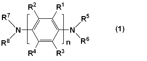

2. 前記R5およびR7が、水素原子であり、前記R6およびR8が、それぞれ独立して、フェニル基(このフェニル基は、ハロゲン原子、ニトロ基、シアノ基、水酸基、チオール基、リン酸基、スルホン酸基、カルボキシル基、炭素数1~20のアルコキシ基、炭素数1~20のチオアルコキシ基、炭素数1~20のアルキル基、炭素数1~20のハロアルキル基、炭素数3~20のシクロアルキル基、炭素数6~20のビシクロアルキル基、炭素数2~20のアルケニル基、炭素数2~20のアルキニル基、炭素数6~20のアリール基、炭素数7~20のアラルキル基、または炭素数1~20のアシル基で置換されていてもよい。)、または前記式(2)で表される基である1の電荷輸送性ワニス、
3. 前記R1~R4が、それぞれ独立して、水素原子、ハロゲン原子、炭素数1~4のアルキル基、炭素数1~4のパーフルオロアルキル基、または炭素数1~4のアルコキシ基であり、前記R5およびR7が、水素原子であり、前記R6およびR8が、それぞれ独立して、フェニル基、または式(2′)で表される基である1または2の電荷輸送性ワニス、

4. 前記nが、2または3である1~3のいずれかの電荷輸送性ワニス、
5. 前記電子受容性ドーパント物質が、アリールスルホン酸化合物を含む1~4のいずれかの電荷輸送性ワニス、
6. 前記電子受容性ドーパント物質が、アリールスルホン酸化合物とヘテロポリ酸化合物との組み合わせである1~5のいずれかの電荷輸送性ワニス、
7. 前記アリールスルホン酸化合物が、式(3)で表される5または6の電荷輸送性ワニス、

8. 前記Xが、Oを表し、前記Aが、ナフタレン環またはアントラセン環を表す7の電荷輸送性ワニス、
9. 1~8のいずれかの電荷輸送性ワニスから作製された電荷輸送性薄膜、
10. 9の電荷輸送性薄膜を備える有機エレクトロルミネッセンス素子、
11. 前記電荷輸送性薄膜が、正孔注入層または正孔輸送層である10の有機エレクトロルミネッセンス素子、
12. 1の電荷輸送性ワニスを用いて電荷輸送性薄膜を作製する工程を有する有機エレクトロルミネッセン素子の製造方法、
13. 前記電荷輸送性薄膜が正孔注入層または正孔輸送層である12の有機エレクトロルミネッセン素子の製造方法、
14. 前記電荷輸送性薄膜を作製する工程が、前記電荷輸送性ワニスを、スピンコート法、スプレー法、インクジェット法またはスリットコート法で塗布して製膜する工程を含む12の有機エレクトロルミネッセンス素子の製造方法
を提供する。
本発明の電荷輸送性ワニスを用いることで、高い透明性および導電性を備えた電荷輸送性薄膜が得られ、この薄膜を、特に有機EL素子の電荷注入層に適用することで、高い発光効率を有し、かつ、耐久性に優れた有機EL素子を得ることができる。
本発明に係る電荷輸送性ワニスは、上記式(1)で表されるアリールジアミン化合物と、電子受容性ドーパント物質と、溶媒とを含むものである。
なお、電荷輸送性とは、正孔輸送性を意味する。本発明の電荷輸送性ワニスは、それ自体に電荷輸送性があるものでもよく、ワニスを使用して得られる固体膜に電荷輸送性があるものでもよい。
炭素数1~20のアルコキシ基の具体例としては、メトキシ基、エトキシ基、n-プロポキシ基、i-プロポキシ基、c-プロポキシ基、n-ブトキシ基、i-ブトキシ基、s-ブトキシ基、t-ブトキシ基、n-ペントキシ基、n-ヘキソキシ基、n-ヘプチルオキシ基、n-オクチルオキシ基、n-ノニルオキシ基、n-デシルオキシ基、n-ウンデシルオキシ基、n-ドデシルオキシ基、n-トリデシルオキシ基、n-テトラデシルオキシ基、n-ペンタデシルオキシ基、n-ヘキサデシルオキシ基、n-ヘプタデシルオキシ基、n-オクタデシルオキシ基、n-ノナデシルオキシ基、n-エイコサニルオキシ基などが挙げられる。
その具体例としては、フルオロメチル基、ジフルオロメチル基、トリフルオロメチル基、ペンタフルオロエチル基、2,2,2-トリフルオロエチル基、ヘプタフルオロプロピル基、2,2,3,3,3-ペンタフルオロプロピル基、2,2,3,3-テトラフルオロプロピル基、2,2,2-トリフルオロ-1-(トリフルオロメチル)エチル基、ノナフルオロブチル基、4,4,4-トリフルオロブチル基、ウンデカフルオロペンチル基、2,2,3,3,4,4,5,5,5-ノナフルオロペンチル基、2,2,3,3,4,4,5,5-オクタフルオロペンチル基、トリデカフルオロヘキシル基、2,2,3,3,4,4,5,5,6,6,6-ウンデカフロオロヘキシル基、2,2,3,3,4,4,5,5,6,6-デカフルオロヘキシル基、3,3,4,4,5,5,6,6,6-ノナフルオロヘキシル基などが挙げられる。
炭素数6~20のビシクロアルキル基の具体例としては、ビシクロプロピル基、ビシクロブチル基、ビシクロペンチル基、ビシクロヘキシル基、ビシクロヘプチル基、ビシクロオクチル基、ビシクロノニル基などが挙げられる。
炭素数7~20のアラルキル基の具体例としては、ベンジル基、フェニルエチル基、フェニルプロピル基、ナフチルメチル基、ナフチルエチル基、ナフチルプロピル基などが挙げられる。
炭素数1~20のアシル基の具体例としては、ホルミル基、アセチル基、プロピオニル基、ブチリル基、イソブチリル基、バレリル基、イソバレリル基、ベンゾイル基などが挙げられる。
なお、R5~R14における、ハロゲン原子、炭素数1~20のアルコキシ基、炭素数1~20のチオアルコキシ基、炭素数1~20のアルキル基、炭素数1~20のハロアルキル基、炭素数3~20のシクロアルキル基、炭素数6~20のビシクロアルキル基、炭素数2~20のアルケニル基、炭素数2~20のアルキニル基、炭素数6~20のアリール基、炭素数7~20のアラルキル基、炭素数1~20のアシル基の具体例としては、上記と同様のものが挙げられる。
これらの中でも、アリールジアミン化合物の溶媒に対する溶解性を高めるとともに、得られる薄膜の均一性を高めることを考慮すると、R13'およびR14'は、それぞれ独立して、フェニル基またはナフチル基であることが好ましく、共にフェニル基であることがより好ましい。

精製したものを用いることで、当該ワニスから得られた薄膜を備えた有機EL素子の特性をより高めることができる。
再結晶にて精製する場合、溶媒としては、例えば、1,4-ジオキサン、テトラヒドロフランなどを用いることができる。
本発明の電荷輸送性ワニスにおいて、式(1)で示される化合物は、式(1)で示されるアリールジアミン化合物から選ばれる1種の化合物(すなわち、分子量分布の分散度が1)を単独で用いてもよく、2以上の化合物を組み合わせて用いてもよい。
Aは、Xおよびp個の(SO3H)基以外の置換基として、ハロゲン原子、ニトロ基、シアノ基、水酸基、チオール基、リン酸基、スルホン酸基、カルボキシル基、炭素数1~20のアルコキシ基、炭素数1~20のチオアルコキシ基、炭素数1~20のアルキル基、炭素数1~20のハロアルキル基、炭素数3~20のシクロアルキル基、炭素数6~20のビシクロアルキル基、炭素数2~20のアルケニル基、炭素数2~20のアルキニル基、炭素数6~20のアリール基、炭素数7~20のアラルキル基および炭素数1~20のアシル基から選ばれる1以上の置換基を有していてもよいナフタレン環またはアントラセン環を表すが、特に、ナフタレン環またはアントラセン環が好ましい。
Bは、2価もしくは3価のベンゼン環、2価のp-キシリレン基、2価もしくは3価のナフタレン環、2~4価のパーフルオロビフェニル基、または2価の2,2-ビス((ヒドロキシプロポキシ)フェニル)プロピル基を表す。
AおよびBにおける、各置換基の具体例としては、上記と同様のものが挙げられる。
pは、Aに結合するスルホン酸基数を表し、1~4を満たす整数である。
qは、BとXとの結合数を示し、2~4を満たす整数である。
ヘテロポリ酸化合物は、代表的に式(A)で示されるKeggin型あるいは式(B)で示されるDawson型の化学構造で示される、ヘテロ原子が分子の中心に位置する構造を有し、バナジウム(V)、モリブデン(Mo)、タングステン(W)等の酸素酸であるイソポリ酸と、異種元素の酸素酸とが縮合してなるポリ酸である。
このような異種元素の酸素酸としては、主にケイ素(Si)、リン(P)、ヒ素(As)の酸素酸が挙げられる。

なお、これらのヘテロポリ酸化合物は、公知の合成法によって合成して用いてもよいが、市販品としても入手可能である。例えば、リンタングステン酸(Phosphotungstic acid hydrate、または12 Tungsto Phosphoric Acid n-hydrate,化学式:H3(PW12O40)・nH2O)や、リンモリブデン酸(Phosphomolybdic acid hydrate、または12 Molybdo(VI) phosphoric acid n-hydrate,化学式:H3(PMo12O40)・nH2O(n≒30))は、関東化学(株)、和光純薬(株)、シグマアルドリッチジャパン(株)、日本無機化学工業(株)、日本新金属(株)等のメーカーから入手可能である。
さらに、固形分の凝集を防止して平坦性の高い薄膜を再現性良く製造することを考慮すると、N,N′-ジフェニルベンジジンと、アリールスルホン酸化合物、好ましくは式(3)で示されるアリールスルホン酸化合物、およびヘテロポリ酸、好ましくはリンタングステン酸の2成分からなる電子受容性ドーパントと、の組み合わせがより好ましい。
なお、ジアリールアミン化合物および電子受容性ドーパント物質は、いずれも上記溶媒に完全に溶解しているか、均一に分散している状態となっていることが好ましい。
高粘度有機溶媒としては、特に限定されるものではなく、例えば、シクロヘキサノール、エチレングリコール、エチレングリコールジクリシジルエーテル、1,3-オクチレングリコール、ジエチレングリコール、ジプロピレングリコール、トリエチレングリコール、トリプロピレングリコール、1,3-ブタンジオール、2,3-ブタンジオール、1,4-ブタンジオール、プロピレングリコール、へキシレングリコール等が挙げられる。
本発明のワニスに用いられる溶媒全体に対する高粘度有機溶媒の添加割合は、固体が析出しない範囲内であることが好ましく、固体が析出しない限りにおいて、添加割合は、5~80質量%であることが好ましい。
このような溶媒としては、例えば、エチレングリコールモノブチルエーテル、ジエチレングリコールジエチルエーテル、ジエチレングリコールジメチルエーテル、ジエチレングリコールモノエチルエーテルアセテート、ジエチレングリコールモノブチルエーテルアセテート、ジプロピレングリコールモノメチルエーテル、プロピレングリコールモノメチルエーテル、プロピレングリコールモノメチルエーテルアセテート、ジエチレングリコールモノエチルエーテル、ジアセトンアルコール、γ-ブチロラクトン、エチルラクテート、n-ヘキシルアセテート等が挙げられるが、これらに限定されるものではない。これらの溶媒は1種単独で、または2種以上混合して用いることができる。
ワニスの塗布方法としては、特に限定されるものではなく、ディップ法、スピンコート法、転写印刷法、ロールコート法、刷毛塗り、インクジェット法、スプレー法等が挙げられる。
溶媒の蒸発法としても特に限定されるものではなく、例えば、ホットプレートやオーブンを用いて、適切な雰囲気下、すなわち大気、窒素等の不活性ガス、真空中等で蒸発させればよい。これにより、均一な成膜面を有する薄膜を得ることが可能である。
焼成温度は、溶媒を蒸発させることができれば特に限定されないが、40~250℃が好ましい。この場合、より高い均一成膜性を発現させたり、基材上で反応を進行させたりする目的で、2段階以上の温度変化をつけてもよい。
使用する電極基板は、洗剤、アルコール、純水等による液体洗浄を予め行って浄化しておくことが好ましく、例えば、陽極基板では使用直前にUVオゾン処理、酸素-プラズマ処理等の表面処理を行うことが好ましい。ただし陽極材料が有機物を主成分とする場合、表面処理を行わなくともよい。
陽極基板上に当該正孔輸送性ワニスを塗布し、上記の方法により蒸発、焼成を行い、電極上に正孔輸送性薄膜を作製する。これを真空蒸着装置内に導入し、正孔輸送層、発光層、電子輸送層、電子注入層、陰極金属を順次蒸着してOLED素子とする。発光領域をコントロールするために任意の層間にキャリアブロック層を設けてもよい。
陽極材料としては、インジウム錫酸化物(ITO)、インジウム亜鉛酸化物(IZO)に代表される透明電極が挙げられ、平坦化処理を行ったものが好ましい。高電荷輸送性を有するポリチオフェン誘導体やポリアニリン誘導体を用いることもできる。
電子輸送材料としては、Alq3、BAlq、DPVBi、(2-(4-ビフェニル)-5-(4-t-ブチルフェニル)-1,3,4-オキサジアゾール)(PBD)、トリアゾール誘導体(TAZ)、バソクプロイン(BCP)、シロール誘導体等が挙げられる。
電子注入層を形成する材料としては、酸化リチウム(Li2O)、酸化マグネシウム(MgO)、アルミナ(Al2O3)、フッ化リチウム(LiF)、フッ化マグネシウム(MgF2)、フッ化ストロンチウム(SrF2)、Liq、Li(acac)、酢酸リチウム、安息香酸リチウム等が挙げられる。
陰極材料としては、アルミニウム、マグネシウム-銀合金、アルミニウム-リチウム合金、リチウム、ナトリウム、カリウム、セシウム等が挙げられる。
上記OLED素子作製において、正孔輸送層、発光層、電子輸送層、電子注入層の真空蒸着操作を行う代わりに、発光性電荷輸送性高分子層を形成することによって本発明の電荷輸送性ワニスによって形成される電荷輸送性薄膜を含むPLED素子を作製することができる。
具体的には、陽極基板上に、電荷輸送性ワニス(正孔輸送性ワニス)を塗布して上記の方法により正孔輸送性薄膜を作製し、その上部に発光性電荷輸送性高分子層を形成し、さらに陰極電極を蒸着してPLED素子とする。
発光性電荷輸送性高分子層の形成法としては、発光性電荷輸送性高分子材料、またはこれに発光性ドーパントを加えた材料に溶媒を加えて溶解するか、均一に分散し、正孔注入層を形成してある電極基板に塗布した後、溶媒の蒸発により成膜する方法が挙げられる。
発光性電荷輸送性高分子材料としては、ポリ(9,9-ジアルキルフルオレン)(PDAF)等のポリフルオレン誘導体、ポリ(2-メトキシ-5-(2’-エチルヘキソキシ)-1,4-フェニレンビニレン)(MEH-PPV)等のポリフェニレンビニレン誘導体、ポリ(3-アルキルチオフェン)(PAT)などのポリチオフェン誘導体、ポリビニルカルバゾール(PVCz)等を挙げることができる。
塗布方法としては、特に限定されるものではなく、インクジェット法、スプレー法、ディップ法、スピンコート法、転写印刷法、ロールコート法、刷毛塗り等が挙げられる。なお、塗布は、窒素、アルゴン等の不活性ガス下で行うことが好ましい。
溶媒の蒸発法としては、不活性ガス下または真空中、オーブンまたはホットプレートで加熱する方法を挙げることができる。
なお、以下において、基板洗浄には長州産業(株)製基板洗浄装置(減圧プラズマ方式)を、ワニス塗布にはミカサ(株)製スピンコーターMS-A100を、膜厚測定には(株)小坂研究所製微細形状測定機サーフコーダET-4000を、透過率測定には(株)島津製作所製可視紫外線吸収スペクトル測定装置UV-3100PCを用いた。
また、OLED素子の作製には長州産業(株)製多機能蒸着装置システムC-E2L1G1-Nを、OLED素子の輝度等の素子特性の測定には(有)テック・ワールド製I-V-L測定システムを、OLED素子の寿命測定には(株)イーエッチシー製有機EL輝寿命度評価システムPEL-105Sを用いた。
[合成例1]
実施例および比較例において使用するNSO-2を、国際公開第2006/025342号の記載に基づき、下記反応式に従い合成した。
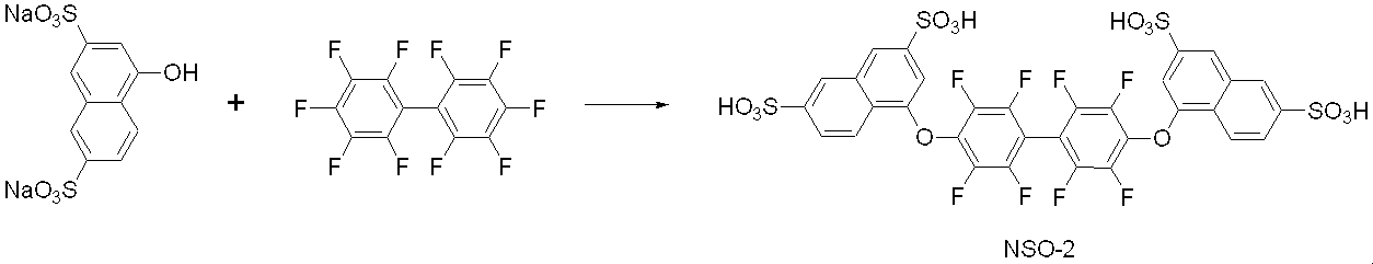
室温まで放冷後、反応後に析出しているNSO-2を再溶解させるために、N,N-ジメチルホルムアミドをさらに500ml加え、室温撹拌を90分間行った。室温撹拌後、この溶液を濾過して炭酸カリウム残渣を除去し、減圧濃縮した。さらに、残存している不純物を除去するために、残渣にメタノール100mlを加え、室温撹拌を行った。室温で30分間撹拌後、懸濁溶液を濾過し、濾物を濾取した。濾物に超純水300mlを加えて溶解し、陽イオン交換樹脂ダウエックス650C(ダウ・ケミカル社製、Hタイプ約200ml、留出溶媒:超純水)を用いたカラムクロマトグラフィーによりイオン交換した。
pH1以下の分画を減圧下で濃縮乾固し、残渣を減圧下で乾固して黄色粉末11gを得た(収率85%)。
比較例において使用するN,N’-ジ(1-n-ブチル)-N,N’-ジフェニル-ベンジジン(DPBZ-C4)を、以下の反応式に従い合成した。

その後、イオン交換水を用いて分液処理を行い、得られた有機層から溶媒を蒸発除去して濃縮した。濃縮液に活性炭およびトルエンを加えて50℃で30分間撹拌後、ろ過により活性炭を除去して得られたろ液から溶媒を蒸発除去した。得られた固体を減圧下で乾燥し、そこにn-ヘキサンを加えてスラリー洗浄をした後、洗浄した固体を再度減圧下で乾燥して粉末4.3gを得た(収率65%)。
1H NMR (300 MHz, CDCl3) δ 7.45 (d, J = 8.4 Hz, 4H), 7.24-7.29 (m, 4H), 6.92-7.04(m, 10H), 3.71 (t, J = 7.5 Hz, 4H), 1.62-1.73 (m, 4H), 1.32-1.44 (m, 4H), 0.93(t, J = 7.5 Hz, 6H).
式[1]で示されるN,N′-ジフェニルベンジジン(東京化成工業(株)製、以下DPBZと略す)を、1,4-ジオキサンを用いて再結晶し、その後、減圧下でよく乾燥した。減圧乾燥したDPBZ0.244g(0.726mmol)と、NSO-2 0.246g(0.272mol)とを、窒素雰囲気下で1,3-ジメチル-2-イミダゾリジノン(以下DMIと略す)8gに溶解させた。得られた溶液に、シクロヘキサノール(以下CHAと略す)12gおよびプロピレングリコール(以下PGと略す)4gを加えて撹拌し、電荷輸送性ワニスを調製した(固形分2.0質量%)。
得られたワニスを、スピンコーターを用いて石英基板に塗布した後、大気中、50℃で5分間乾燥し、さらに230℃で15分間焼成し、石英基板上に膜厚30nmの均一な薄膜を形成した。
なお、石英基板は、プラズマ洗浄装置(150W、30秒間)を用いて表面上の不純物を除却してから使用した(以下同様)。

DPBZの使用量を0.163g(0.485mmol)とし、NSO-2 0.246gの代わりに、NSO-2 0.229g(0.253mmol)およびリンタングステン酸(関東化学(株)製)0.098g(0.034mmol)を用いた以外は、実施例1-1と同様の方法で、石英基板上に膜厚30nmの均一な薄膜を形成した。
NSO-2の使用量およびリンタングステン酸の使用量を、それぞれ、0.196g(0.217mmol),0.131g(0.045mmol)(実施例1-3)、0.163g(0.181mmol),0.163g(0.057mmol)(実施例1-4)、0.131g(0.145mmol),0.196g(0.068mmol)(実施例1-5)、0.098g(0.109mmol),0.229g(0.079mmol)(実施例1-6)とした以外は、実施例1-2と同様の方法で、石英基板上に膜厚30nmの均一な薄膜を形成した。
DPBZの使用量、NSO-2の使用量およびリンタングステン酸の使用量を、それぞれ、0.122g(0.364mmol),0.184g(0.203mmol),0.184g(0.064mmol)(実施例1-7)、0.122g(0.364mmol),0.147g(0.163mmol),0.220g(0.077mmol)(実施例1-8)、0.122g(0.364mmol),0.110g(0.122mmol),0.257g(0.089mmol)(実施例1-9)とした以外は、実施例1-2と同様の方法で、石英基板上に膜厚30nmの均一な薄膜を形成した。
国際公開第2008/032616号記載の方法に従って製造した式[2]で示されるビス(4-ジフェニルアミノ)-2,2′-ジメチル-4,4′-ジアミノビフェニル(以下BDDMDと略す)0.185g(0.338mmol)と、NSO-2 0.305g(0.338mmol)とを窒素雰囲気下でDMI8gに完全に溶解させた。得られた溶液に、CHA12gおよびPG4gを加えて撹拌し、電荷輸送性ワニスを調製した(固形分2.0質量%)。
得られたワニスを、スピンコーターを用いて石英基板に塗布した後、実施例1-1と同様にして乾燥および焼成し、石英基板上に膜厚30nmの均一な薄膜を形成した。
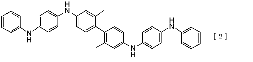
国際公開第2008/032616号記載の方法に従って製造した式[3]で示される(4-ジフェニルアミノ)-4,4′-ジアミノジフェニルエーテル(以下BDDEと略す)と、NSO-2 0.308g(0.341mmol)とを窒素雰囲気下でDMI8gに完全に溶解させた。得られた溶液に、CHA12gおよびPG4gを加えて撹拌し、電荷輸送性ワニスを調製した(固形分2.0質量%)。
得られたワニスを、スピンコーターを用いて石英基板に塗布した後、実施例1-1と同様にして乾燥および焼成を行い、石英基板上に膜厚30nmの均一な薄膜を形成した。
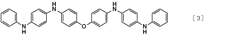
比較合成例1で合成した式[4]で示されるDPBZ-C4 0.279g(0.622mmol)と、NSO-2 0.211g(0.233mmol)とを、窒素雰囲気下でDMI8gに溶解させた。得られた溶液に、CHA12gおよびPG4gを加えて撹拌し、電荷輸送性ワニスを調製した(固形分2.0質量%)。
得られたワニスを、スピンコーターを用いて石英基板に塗布した後、実施例1-1と同様にして乾燥および焼成し、石英基板上に膜厚30nmの均一な薄膜を形成した。
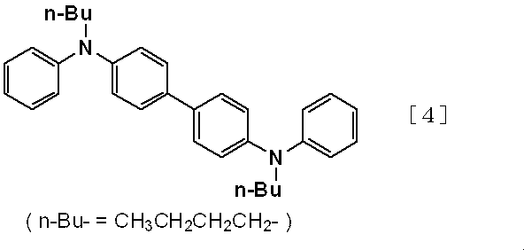

透明性向上の理由としては、実施例の薄膜に含まれるDPBZが、比較例1,2で用いたBDDMD、BDDEがとり得る、透明性の低下の要因と考えられるキノイド構造をとらないことが考えられる。
このことは、DPBZと極めて類似する構造を有し、同様にキノイド構造をとらないDPBZ-C6を用いて作製した薄膜(比較例3)が、高い透明性を有することからも示唆される。
なお、キノイド構造とは、芳香族化合物の炭素環内の二重結合が一つ減り、代わりにパラあるいはオルト位に環外二重結合2個を持つ構造である。例えば、互いにパラ位にある2つのアミノ基を有するアリールジアミン化合物であれば、式[5]に示すような構造となる。
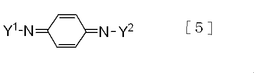
電気特性を評価する際の基板には、インジウム錫酸化物が表面上に膜厚150nmでパターニングされた25mm×25mm×0.7tのガラス基板(以下ITO基板と略す)を用いた。ITO基板は、O2プラズマ洗浄装置(150W、30秒間)を用いて表面上の不純物を除去してから使用した。
実施例1-1で得られたワニスを、スピンコーターを用いてITO基板に塗布した後、50℃で5分間乾燥し、さらに230℃で15分間焼成し、ITO基板上に30nmの均一な薄膜を形成した。
次いで、薄膜を形成したITO基板に対し、蒸着装置を用いてアルミニウム薄膜を形成して単層素子を得た。アルミニウム薄膜の膜厚は120nmとし、蒸着は、真空度1.3×10⁻³Pa、蒸着レート0.2nm/秒の条件で行った。
なお、空気中の酸素、水等の影響による特性劣化を防止するため、単層素子は封止基板により封止した後、その特性を評価した。封止は、以下の手順で行った。
酸素濃度2ppm以下、露点-85℃以下の窒素雰囲気中で、単層素子を封止基板の間に収め、封止基板を接着材により貼り合わせた。この際、保水剤としてダイニック(株)製HD-071010W-40を単層素子と共に封止基板内に収めた。接着材としては、ナガセケムテックス(株)製XNR5516Z-B1を使用した。
貼り合わせた封止基板に対し、UV光を照射(波長:365nm、照射量:6000mJ/cm2)した後、80℃で1時間、アニーリング処理して接着材を硬化させた。
比較例1,2で得られたワニスをそれぞれ用いた以外は、実施例2-1と同様の方法で単層素子を作製した。

ポリアニリン等のポリアリールアミン化合物においては、通常、分子中のキノイド構造が薄膜の導電率向上に大きく貢献していると考えられていることに鑑みれば、実施例1-1のワニスに含まれる、キノイド構造をとらないDPBZのような化合物を用いて電荷輸送性薄膜を作製した場合には、その導電性が顕著に低下すると推測される。
しかし、上記図3および表2のデータは、DPBZを含む薄膜が、キノイド構造をとり得ないにも関わらず、キノイド構造をとるBDDMDおよびBDDEを含む薄膜よりも優れた導電性を発揮することを示しており、上記推測とは異なる結果が得られていることは明らかである。
以上のように、実施例1-1のワニスから得られた薄膜は、高い透明性を示し、またキノイド構造をとり得ないにも関わらず高い導電性を発揮するものである。
[実施例3-1]
実施例1-1で得られたワニスおよび実施例2-1と同様の基板を用い、実施例2-1と同様の方法でITO基板上に30nmの均一な薄膜を形成した。
薄膜を形成したITO基板に対し、蒸着装置を用いてα-NPD、Alq3、フッ化リチウム、およびアルミニウムの薄膜を順次積層し、OLED素子を得た。膜厚は、それぞれ30nm、40nm、0.5nmおよび120nmとし、真空度1.3×10⁻³Pa、蒸着レートはLiFでは0.02nm/秒、それ以外の材料では0.2nm/秒の条件で蒸着を行った。
なお、OLED素子は、実施例2-1と同様の方法で封止した。
実施例1-2~1-9で得られたワニスをそれぞれ用いた以外は、実施例3-1と同様の方法でOLED素子を作製した。
比較例1~3で得られたワニスをそれぞれ用いた以外は、実施例3-1と同様の方法でOLED素子を作製した。
ワニスを用いて薄膜を形成する代わりに、DPBZを蒸着源とする蒸着法(蒸着レート0.2nm/秒)で、ITO基板上にDPBZのみからなる30nmの均一な薄膜を形成した以外は、実施例3-1と同様の方法でOLED素子を作製した。

実施例1-1~1-9のワニスを用いて作製した薄膜が優れた透明性を備えていることは判明していたが、表3および図6,7に示されるように、上記式[1]で示される化合物と電子受容性ドーパント物質を組み合わせて用いることで初めて、優れた透明性と優れた輝度特性を実現できる薄膜が製造できることがわかる。
駆動時間に対する駆動電圧の挙動を図8に、駆動時間に対する輝度の減衰(初期輝度を1とする)を図9に、各OLED素子の初期輝度、駆動電流、半減期、初期および輝度半減駆動電圧、並びに電圧上昇値を表4に示す

このように、実施例3-1~3-3で作製したOLED素子は、良好な発光特性を有するだけでなく、高い耐久性をも備えていることがわかる。
Claims (14)
- 式(1)で表されるアリールジアミン化合物と、電子受容性ドーパント物質と、溶媒とを含むことを特徴とする電荷輸送性ワニス。

R5~R8は、それぞれ独立して、水素原子、フェニル基、ナフチル基、ピリジル基、ピリミジニル基、ピリダジニル基、ピラジニル基、フラニル基、ピロリル基、ピラゾリル基、イミダゾリル基、チエニル基(これらの基は、ハロゲン原子、ニトロ基、シアノ基、水酸基、チオール基、リン酸基、スルホン酸基、カルボキシル基、炭素数1~20のアルコキシ基、炭素数1~20のチオアルコキシ基、炭素数1~20のアルキル基、炭素数1~20のハロアルキル基、炭素数3~20のシクロアルキル基、炭素数6~20のビシクロアルキル基、炭素数2~20のアルケニル基、炭素数2~20のアルキニル基、炭素数6~20のアリール基、炭素数7~20のアラルキル基または炭素数1~20のアシル基で置換されていてもよい。)、または式(2)で表される基を表し(ただし、R5~R8の少なくとも1つは水素原子である。)、

R13およびR14は、それぞれ独立して、フェニル基、ナフチル基、アントリル基、ピリジル基、ピリミジニル基、ピリダジニル基、ピラジニル基、フラニル基、ピロリル基、ピラゾリル基、イミダゾリル基、チエニル基(これらの基は、互いに結合して環を形成してもよく、また、ハロゲン原子、ニトロ基、シアノ基、水酸基、チオール基、リン酸基、スルホン酸基、カルボキシル基、炭素数1~20のアルコキシ基、炭素数1~20のチオアルコキシ基、炭素数1~20のアルキル基、炭素数1~20のハロアルキル基、炭素数3~20のシクロアルキル基、炭素数6~20のビシクロアルキル基、炭素数2~20のアルケニル基、炭素数2~20のアルキニル基、炭素数6~20のアリール基、炭素数7~20のアラルキル基、または炭素数1~20のアシル基で置換されていてもよい。)〕
nは、2~5の整数を表す。} - 前記R5およびR7が、水素原子であり、
前記R6およびR8が、それぞれ独立して、フェニル基(このフェニル基は、ハロゲン原子、ニトロ基、シアノ基、水酸基、チオール基、リン酸基、スルホン酸基、カルボキシル基、炭素数1~20のアルコキシ基、炭素数1~20のチオアルコキシ基、炭素数1~20のアルキル基、炭素数1~20のハロアルキル基、炭素数3~20のシクロアルキル基、炭素数6~20のビシクロアルキル基、炭素数2~20のアルケニル基、炭素数2~20のアルキニル基、炭素数6~20のアリール基、炭素数7~20のアラルキル基、または炭素数1~20のアシル基で置換されていてもよい。)、または前記式(2)で表される基である請求項1記載の電荷輸送性ワニス。 - 前記R1~R4が、それぞれ独立して、水素原子、ハロゲン原子、炭素数1~4のアルキル基、炭素数1~4のパーフルオロアルキル基、または炭素数1~4のアルコキシ基であり、
前記R5およびR7が、水素原子であり、
前記R6およびR8が、それぞれ独立して、フェニル基、または式(2′)で表される基である請求項1または2記載の電荷輸送性ワニス。

- 前記nが、2または3である請求項1~3のいずれか1項記載の電荷輸送性ワニス。
- 前記電子受容性ドーパント物質が、アリールスルホン酸化合物を含む請求項1~4のいずれか1項記載の電荷輸送性ワニス。
- 前記電子受容性ドーパント物質が、アリールスルホン酸化合物とヘテロポリ酸化合物との組み合わせである請求項1~5のいずれか1項記載の電荷輸送性ワニス。
- 前記アリールスルホン酸化合物が、式(3)で表される請求項5または6記載の電荷輸送性ワニス。

Aは、Xおよびp個の(SO3H)基以外の置換基として、ハロゲン原子、ニトロ基、シアノ基、水酸基、チオール基、リン酸基、スルホン酸基、カルボキシル基、炭素数1~20のアルコキシ基、炭素数1~20のチオアルコキシ基、炭素数1~20のアルキル基、炭素数1~20のハロアルキル基、炭素数3~20のシクロアルキル基、炭素数6~20のビシクロアルキル基、炭素数2~20のアルケニル基、炭素数2~20のアルキニル基、炭素数6~20のアリール基、炭素数7~20のアラルキル基および炭素数1~20のアシル基から選ばれる1以上の置換基を有していてもよいナフタレン環またはアントラセン環を表し、
Bは、2価もしくは3価のベンゼン環、2価のp-キシリレン基、2価もしくは3価のナフタレン環、2~4価のパーフルオロビフェニル基、または2価の2,2-ビス((ヒドロキシプロポキシ)フェニル)プロピル基を表し、
pは、Aに結合するスルホン酸基数を表し、1~4を満たす整数であり、
qは、BとXとの結合数を示し、2~4を満たす整数である。〕 - 前記Xが、Oを表し、前記Aが、ナフタレン環またはアントラセン環を表す請求項7記載の電荷輸送性ワニス。
- 請求項1~8のいずれか1項記載の電荷輸送性ワニスから作製された電荷輸送性薄膜。
- 請求項9記載の電荷輸送性薄膜を備える有機エレクトロルミネッセンス素子。
- 前記電荷輸送性薄膜が、正孔注入層または正孔輸送層である請求項10記載の有機エレクトロルミネッセンス素子。
- 請求項1記載の電荷輸送性ワニスを用いて電荷輸送性薄膜を作製する工程を有する、有機エレクトロルミネッセン素子の製造方法。
- 前記電荷輸送性薄膜が正孔注入層または正孔輸送層である請求項12記載の有機エレクトロルミネッセン素子の製造方法。
- 前記電荷輸送性薄膜を作製する工程が、前記電荷輸送性ワニスを、スピンコート法、スプレー法、インクジェット法またはスリットコート法で塗布して製膜する工程を含む請求項12記載の有機エレクトロルミネッセンス素子の製造方法。
Priority Applications (5)
| Application Number | Priority Date | Filing Date | Title |
|---|---|---|---|
| EP12833167.5A EP2759574B1 (en) | 2011-09-21 | 2012-09-14 | Charge-transporting varnish |
| CN201280045988.2A CN103814091B (zh) | 2011-09-21 | 2012-09-14 | 电荷传输性清漆 |
| KR1020147009724A KR101641674B1 (ko) | 2011-09-21 | 2012-09-14 | 전하수송성 바니시 |
| JP2013534697A JP5761357B2 (ja) | 2011-09-21 | 2012-09-14 | 塗布型電荷輸送性薄膜形成用ワニス |
| US14/346,115 US9444052B2 (en) | 2011-09-21 | 2012-09-14 | Charge-transporting varnish |
Applications Claiming Priority (2)
| Application Number | Priority Date | Filing Date | Title |
|---|---|---|---|
| JP2011-205430 | 2011-09-21 | ||
| JP2011205430 | 2011-09-21 |
Publications (1)
| Publication Number | Publication Date |
|---|---|
| WO2013042623A1 true WO2013042623A1 (ja) | 2013-03-28 |
Family
ID=47914392
Family Applications (1)
| Application Number | Title | Priority Date | Filing Date |
|---|---|---|---|
| PCT/JP2012/073602 WO2013042623A1 (ja) | 2011-09-21 | 2012-09-14 | 電荷輸送性ワニス |
Country Status (7)
| Country | Link |
|---|---|
| US (1) | US9444052B2 (ja) |
| EP (1) | EP2759574B1 (ja) |
| JP (1) | JP5761357B2 (ja) |
| KR (1) | KR101641674B1 (ja) |
| CN (2) | CN106025098B (ja) |
| TW (1) | TWI596136B (ja) |
| WO (1) | WO2013042623A1 (ja) |
Cited By (36)
| Publication number | Priority date | Publication date | Assignee | Title |
|---|---|---|---|---|
| WO2014132834A1 (ja) * | 2013-02-26 | 2014-09-04 | 日産化学工業株式会社 | 電荷輸送性ワニス |
| WO2014148415A1 (ja) * | 2013-03-18 | 2014-09-25 | 日産化学工業株式会社 | 電荷輸送性ワニス |
| WO2014185208A1 (ja) * | 2013-05-17 | 2014-11-20 | 日産化学工業株式会社 | 電荷輸送性ワニス |
| WO2015050253A1 (ja) | 2013-10-04 | 2015-04-09 | 日産化学工業株式会社 | アニリン誘導体およびその利用 |
| WO2015053320A1 (ja) | 2013-10-09 | 2015-04-16 | 日産化学工業株式会社 | アリールスルホン酸化合物及びその利用並びにアリールスルホン酸化合物の製造方法 |
| JP2015092560A (ja) * | 2013-10-04 | 2015-05-14 | 日産化学工業株式会社 | 電荷輸送性ワニス、電荷輸送性薄膜、有機エレクトロルミネッセンス素子、及び電荷輸送性薄膜の製造方法 |
| WO2015087797A1 (ja) * | 2013-12-09 | 2015-06-18 | 日産化学工業株式会社 | 有機薄膜太陽電池の陽極バッファ層用組成物及び有機薄膜太陽電池 |
| WO2016006673A1 (ja) * | 2014-07-11 | 2016-01-14 | 日産化学工業株式会社 | 電荷輸送性ワニス |
| CN106030843A (zh) * | 2014-02-18 | 2016-10-12 | 日产化学工业株式会社 | 电荷传输性清漆 |
| WO2016170998A1 (ja) * | 2015-04-22 | 2016-10-27 | 日産化学工業株式会社 | 電荷輸送性膜の製造方法、電荷輸送性膜、有機エレクトロルミネッセンス素子、有機エレクトロルミネッセンス素子の製造方法、電荷輸送性膜の電荷輸送性の向上方法 |
| CN106103410A (zh) * | 2014-03-14 | 2016-11-09 | 日产化学工业株式会社 | 苯胺衍生物及其利用 |
| CN106103411A (zh) * | 2014-03-14 | 2016-11-09 | 日产化学工业株式会社 | 苯胺衍生物及其利用 |
| KR20170013289A (ko) | 2014-05-30 | 2017-02-06 | 닛산 가가쿠 고교 가부시키 가이샤 | 박막의 평탄화 방법, 평탄화 박막의 형성 방법 및 박막 형성용 바니시 |
| KR20170017929A (ko) | 2014-06-05 | 2017-02-15 | 닛산 가가쿠 고교 가부시키 가이샤 | 전하 수송성 바니시 |
| KR20170052560A (ko) | 2014-09-10 | 2017-05-12 | 닛산 가가쿠 고교 가부시키 가이샤 | 전하 수송성 바니시 |
| WO2017135117A1 (ja) | 2016-02-03 | 2017-08-10 | 日産化学工業株式会社 | 電荷輸送性ワニス |
| WO2017150412A1 (ja) | 2016-03-03 | 2017-09-08 | 日産化学工業株式会社 | 電荷輸送性ワニス |
| CN107210378A (zh) * | 2015-01-21 | 2017-09-26 | 日产化学工业株式会社 | 电荷传输性清漆、电荷传输性薄膜和有机电致发光元件 |
| WO2017164158A1 (ja) | 2016-03-24 | 2017-09-28 | 日産化学工業株式会社 | アリールアミン誘導体とその利用 |
| KR20170128409A (ko) * | 2015-03-17 | 2017-11-22 | 닛산 가가쿠 고교 가부시키 가이샤 | 광센서 소자의 정공 포집층 형성용 조성물 및 광센서 소자 |
| KR20180021068A (ko) | 2015-06-15 | 2018-02-28 | 닛산 가가쿠 고교 가부시키 가이샤 | 전하 수송성 바니시 및 유기 일렉트로루미네슨스 소자 |
| WO2018147204A1 (ja) | 2017-02-07 | 2018-08-16 | 日産化学工業株式会社 | 電荷輸送性ワニス |
| WO2018186340A1 (ja) | 2017-04-05 | 2018-10-11 | 日産化学株式会社 | 電荷輸送性ワニス |
| WO2018216507A1 (ja) | 2017-05-25 | 2018-11-29 | 日産化学株式会社 | 電荷輸送性薄膜の製造方法 |
| WO2019124412A1 (ja) | 2017-12-20 | 2019-06-27 | 日産化学株式会社 | スルホン酸エステル化合物及びその利用 |
| WO2020022211A1 (ja) | 2018-07-24 | 2020-01-30 | 日産化学株式会社 | 電荷輸送性組成物 |
| WO2020066979A1 (ja) | 2018-09-25 | 2020-04-02 | 日産化学株式会社 | 有機機能膜付き基板の製造方法 |
| KR20210040081A (ko) | 2018-08-03 | 2021-04-12 | 닛산 가가쿠 가부시키가이샤 | 전하 수송성 조성물 |
| KR20210040393A (ko) | 2018-08-03 | 2021-04-13 | 닛산 가가쿠 가부시키가이샤 | 아닐린 유도체 |
| KR20210144758A (ko) | 2019-03-27 | 2021-11-30 | 닛산 가가쿠 가부시키가이샤 | 아릴아민 화합물 및 그 이용 |
| KR20210144750A (ko) | 2019-03-29 | 2021-11-30 | 닛산 가가쿠 가부시키가이샤 | 플루오렌 유도체 및 그 이용 |
| KR20210151082A (ko) | 2019-03-29 | 2021-12-13 | 닛산 가가쿠 가부시키가이샤 | 전하수송성 바니시 |
| KR20220016122A (ko) | 2019-05-31 | 2022-02-08 | 닛산 가가쿠 가부시키가이샤 | 아릴아민 화합물 및 그 이용 |
| KR20220027970A (ko) | 2019-06-26 | 2022-03-08 | 닛산 가가쿠 가부시키가이샤 | 전하 수송성 바니시 |
| WO2023080024A1 (ja) * | 2021-11-02 | 2023-05-11 | 日産化学株式会社 | 電荷輸送性組成物 |
| KR20230161502A (ko) | 2021-03-29 | 2023-11-27 | 닛산 가가쿠 가부시키가이샤 | 폴리머 및 그 이용 |
Families Citing this family (5)
| Publication number | Priority date | Publication date | Assignee | Title |
|---|---|---|---|---|
| KR20170027790A (ko) | 2014-07-09 | 2017-03-10 | 닛산 가가쿠 고교 가부시키 가이샤 | 전하 수송성 바니시, 전하 수송성 박막 및 그 제조 방법, 그리고 유기 일렉트로 루미네선스 소자 및 그 제조 방법 |
| EP3252840B1 (en) * | 2015-01-20 | 2020-03-11 | Nissan Chemical Corporation | Varnish for formation of charge-transporting thin film |
| US10770659B2 (en) * | 2015-11-06 | 2020-09-08 | Nissan Chemical Industries, Ltd. | Composition for hole trapping layer of organic photoelectric conversion element |
| EP3544072A4 (en) * | 2016-12-16 | 2019-11-27 | Nissan Chemical Corporation | COMPOSITION FOR COLLECTING LAYER OF ORGANIC PHOTOELECTRIC CONVERSION ELEMENT HOLES |
| KR102138411B1 (ko) | 2017-07-07 | 2020-07-27 | 주식회사 엘지화학 | 화합물을 포함하는 코팅 조성물 및 이를 포함하는 유기 발광 소자 |
Citations (10)
| Publication number | Priority date | Publication date | Assignee | Title |
|---|---|---|---|---|
| JPH02195681A (ja) * | 1989-01-24 | 1990-08-02 | Nippon Telegr & Teleph Corp <Ntt> | 薄膜発光素子の製造方法 |
| JPH1088123A (ja) | 1996-09-17 | 1998-04-07 | Sony Corp | 有機電界発光素子 |
| JP2002151272A (ja) | 2000-11-09 | 2002-05-24 | Nissan Chem Ind Ltd | 電界発光素子 |
| WO2005000832A1 (ja) | 2003-06-25 | 2005-01-06 | Nissan Chemical Industries, Ltd. | 1,4-ベンゾジオキサンスルホン酸化合物及び電子受容性物質としての利用 |
| JP2005108828A (ja) | 2003-09-11 | 2005-04-21 | Nissan Chem Ind Ltd | 電荷輸送性ワニス、電荷輸送性薄膜および有機エレクトロルミネッセンス素子 |
| WO2006025342A1 (ja) | 2004-08-31 | 2006-03-09 | Nissan Chemical Industries, Ltd. | アリールスルホン酸化合物及び電子受容性物質としての利用 |
| WO2008032616A1 (en) | 2006-09-13 | 2008-03-20 | Nissan Chemical Industries, Ltd. | Oligoaniline compounds |
| WO2010058777A1 (ja) * | 2008-11-19 | 2010-05-27 | 日産化学工業株式会社 | 電荷輸送性材料および電荷輸送性ワニス |
| JP2010225950A (ja) * | 2009-03-25 | 2010-10-07 | Toyo Ink Mfg Co Ltd | 重合体を用いた有機エレクトロルミネッセンス素子 |
| JP2010229280A (ja) * | 2009-03-27 | 2010-10-14 | Toyo Ink Mfg Co Ltd | 重合体、導電層および電子デバイス |
Family Cites Families (7)
| Publication number | Priority date | Publication date | Assignee | Title |
|---|---|---|---|---|
| US6309763B1 (en) * | 1997-05-21 | 2001-10-30 | The Dow Chemical Company | Fluorene-containing polymers and electroluminescent devices therefrom |
| TW200502277A (en) * | 2003-05-20 | 2005-01-16 | Nissan Chemical Ind Ltd | Charge-transporting varnish |
| JP5230942B2 (ja) * | 2003-12-13 | 2013-07-10 | メルク パテント ゲーエムベーハー | オリゴマーおよびポリマー |
| JP5374819B2 (ja) * | 2004-07-09 | 2013-12-25 | 日産化学工業株式会社 | オリゴアニリン化合物の精製方法およびオリゴアニリン化合物 |
| US8357770B2 (en) | 2006-09-13 | 2013-01-22 | Nissan Chemical Industries, Ltd. | Oligoaniline compound and use thereof |
| KR101557109B1 (ko) * | 2007-04-12 | 2015-10-02 | 닛산 가가쿠 고교 가부시키 가이샤 | 올리고아닐린 화합물 |
| JP5391998B2 (ja) * | 2009-10-22 | 2014-01-15 | 東洋インキScホールディングス株式会社 | 緑色着色組成物、カラーフィルタおよびカラー表示装置 |
-
2012
- 2012-09-14 JP JP2013534697A patent/JP5761357B2/ja active Active
- 2012-09-14 CN CN201610319620.0A patent/CN106025098B/zh active Active
- 2012-09-14 WO PCT/JP2012/073602 patent/WO2013042623A1/ja active Application Filing
- 2012-09-14 US US14/346,115 patent/US9444052B2/en active Active
- 2012-09-14 KR KR1020147009724A patent/KR101641674B1/ko not_active Application Discontinuation
- 2012-09-14 EP EP12833167.5A patent/EP2759574B1/en not_active Expired - Fee Related
- 2012-09-14 CN CN201280045988.2A patent/CN103814091B/zh active Active
- 2012-09-21 TW TW101134744A patent/TWI596136B/zh active
Patent Citations (10)
| Publication number | Priority date | Publication date | Assignee | Title |
|---|---|---|---|---|
| JPH02195681A (ja) * | 1989-01-24 | 1990-08-02 | Nippon Telegr & Teleph Corp <Ntt> | 薄膜発光素子の製造方法 |
| JPH1088123A (ja) | 1996-09-17 | 1998-04-07 | Sony Corp | 有機電界発光素子 |
| JP2002151272A (ja) | 2000-11-09 | 2002-05-24 | Nissan Chem Ind Ltd | 電界発光素子 |
| WO2005000832A1 (ja) | 2003-06-25 | 2005-01-06 | Nissan Chemical Industries, Ltd. | 1,4-ベンゾジオキサンスルホン酸化合物及び電子受容性物質としての利用 |
| JP2005108828A (ja) | 2003-09-11 | 2005-04-21 | Nissan Chem Ind Ltd | 電荷輸送性ワニス、電荷輸送性薄膜および有機エレクトロルミネッセンス素子 |
| WO2006025342A1 (ja) | 2004-08-31 | 2006-03-09 | Nissan Chemical Industries, Ltd. | アリールスルホン酸化合物及び電子受容性物質としての利用 |
| WO2008032616A1 (en) | 2006-09-13 | 2008-03-20 | Nissan Chemical Industries, Ltd. | Oligoaniline compounds |
| WO2010058777A1 (ja) * | 2008-11-19 | 2010-05-27 | 日産化学工業株式会社 | 電荷輸送性材料および電荷輸送性ワニス |
| JP2010225950A (ja) * | 2009-03-25 | 2010-10-07 | Toyo Ink Mfg Co Ltd | 重合体を用いた有機エレクトロルミネッセンス素子 |
| JP2010229280A (ja) * | 2009-03-27 | 2010-10-14 | Toyo Ink Mfg Co Ltd | 重合体、導電層および電子デバイス |
Non-Patent Citations (1)
| Title |
|---|
| See also references of EP2759574A4 |
Cited By (68)
| Publication number | Priority date | Publication date | Assignee | Title |
|---|---|---|---|---|
| US10069075B2 (en) | 2013-02-26 | 2018-09-04 | Nissan Chemical Industries, Ltd. | Charge-transporting varnish |
| WO2014132834A1 (ja) * | 2013-02-26 | 2014-09-04 | 日産化学工業株式会社 | 電荷輸送性ワニス |
| WO2014148415A1 (ja) * | 2013-03-18 | 2014-09-25 | 日産化学工業株式会社 | 電荷輸送性ワニス |
| JPWO2014148415A1 (ja) * | 2013-03-18 | 2017-02-16 | 日産化学工業株式会社 | 電荷輸送性ワニス |
| WO2014185208A1 (ja) * | 2013-05-17 | 2014-11-20 | 日産化学工業株式会社 | 電荷輸送性ワニス |
| CN105210207A (zh) * | 2013-05-17 | 2015-12-30 | 日产化学工业株式会社 | 电荷传输性清漆 |
| JPWO2014185208A1 (ja) * | 2013-05-17 | 2017-02-23 | 日産化学工業株式会社 | 電荷輸送性ワニス |
| KR20160010488A (ko) | 2013-05-17 | 2016-01-27 | 닛산 가가쿠 고교 가부시키 가이샤 | 전하 수송성 바니시 |
| WO2015050253A1 (ja) | 2013-10-04 | 2015-04-09 | 日産化学工業株式会社 | アニリン誘導体およびその利用 |
| JP2015092560A (ja) * | 2013-10-04 | 2015-05-14 | 日産化学工業株式会社 | 電荷輸送性ワニス、電荷輸送性薄膜、有機エレクトロルミネッセンス素子、及び電荷輸送性薄膜の製造方法 |
| WO2015053320A1 (ja) | 2013-10-09 | 2015-04-16 | 日産化学工業株式会社 | アリールスルホン酸化合物及びその利用並びにアリールスルホン酸化合物の製造方法 |
| WO2015087797A1 (ja) * | 2013-12-09 | 2015-06-18 | 日産化学工業株式会社 | 有機薄膜太陽電池の陽極バッファ層用組成物及び有機薄膜太陽電池 |
| US10020449B2 (en) | 2013-12-09 | 2018-07-10 | Nissan Chemical Industries, Ltd. | Composition for anode buffer layer of organic thin film solar cell and organic thin film solar cell |
| KR102252204B1 (ko) * | 2013-12-09 | 2021-05-14 | 닛산 가가쿠 가부시키가이샤 | 유기 박막 태양전지의 양극 버퍼층용 조성물 및 유기 박막 태양전지 |
| EP3082171A4 (en) * | 2013-12-09 | 2017-08-09 | Nissan Chemical Industries, Ltd. | Composition for anode buffer layer of organic thin film solar cell and organic thin film solar cell |
| CN105934836A (zh) * | 2013-12-09 | 2016-09-07 | 日产化学工业株式会社 | 有机薄膜太阳能电池的阳极缓冲层用组合物及有机薄膜太阳能电池 |
| KR20160096637A (ko) * | 2013-12-09 | 2016-08-16 | 닛산 가가쿠 고교 가부시키 가이샤 | 유기 박막 태양전지의 양극 버퍼층용 조성물 및 유기 박막 태양전지 |
| CN106030843A (zh) * | 2014-02-18 | 2016-10-12 | 日产化学工业株式会社 | 电荷传输性清漆 |
| CN106030843B (zh) * | 2014-02-18 | 2019-01-18 | 日产化学工业株式会社 | 电荷传输性清漆 |
| CN106103411A (zh) * | 2014-03-14 | 2016-11-09 | 日产化学工业株式会社 | 苯胺衍生物及其利用 |
| TWI660944B (zh) * | 2014-03-14 | 2019-06-01 | 日商日產化學工業股份有限公司 | 苯胺衍生物及其利用 |
| JPWO2015137384A1 (ja) * | 2014-03-14 | 2017-04-06 | 日産化学工業株式会社 | アニリン誘導体およびその利用 |
| CN106103411B (zh) * | 2014-03-14 | 2020-10-30 | 日产化学工业株式会社 | 苯胺衍生物及其利用 |
| CN106103410A (zh) * | 2014-03-14 | 2016-11-09 | 日产化学工业株式会社 | 苯胺衍生物及其利用 |
| KR20170013289A (ko) | 2014-05-30 | 2017-02-06 | 닛산 가가쿠 고교 가부시키 가이샤 | 박막의 평탄화 방법, 평탄화 박막의 형성 방법 및 박막 형성용 바니시 |
| US10128444B2 (en) | 2014-05-30 | 2018-11-13 | Nissan Chemical Industries, Ltd. | Thin-film planarization method, planarized thin-film formation method, and thin-film formation varnish |
| US11018303B2 (en) | 2014-06-05 | 2021-05-25 | Nissan Chemical Industries, Ltd. | Charge-transporting varnish |
| KR20170017929A (ko) | 2014-06-05 | 2017-02-15 | 닛산 가가쿠 고교 가부시키 가이샤 | 전하 수송성 바니시 |
| JP2020170876A (ja) * | 2014-07-11 | 2020-10-15 | 日産化学株式会社 | 電荷輸送性ワニス |
| JP7161507B2 (ja) | 2014-07-11 | 2022-10-26 | 日産化学株式会社 | 電荷輸送性ワニス |
| JPWO2016006673A1 (ja) * | 2014-07-11 | 2017-04-27 | 日産化学工業株式会社 | 電荷輸送性ワニス |
| KR20170029529A (ko) | 2014-07-11 | 2017-03-15 | 닛산 가가쿠 고교 가부시키 가이샤 | 전하 수송성 바니시 |
| WO2016006673A1 (ja) * | 2014-07-11 | 2016-01-14 | 日産化学工業株式会社 | 電荷輸送性ワニス |
| KR20170052560A (ko) | 2014-09-10 | 2017-05-12 | 닛산 가가쿠 고교 가부시키 가이샤 | 전하 수송성 바니시 |
| CN107210378A (zh) * | 2015-01-21 | 2017-09-26 | 日产化学工业株式会社 | 电荷传输性清漆、电荷传输性薄膜和有机电致发光元件 |
| CN107210378B (zh) * | 2015-01-21 | 2019-11-26 | 日产化学工业株式会社 | 电荷传输性清漆、电荷传输性薄膜和有机电致发光元件 |
| KR20170128409A (ko) * | 2015-03-17 | 2017-11-22 | 닛산 가가쿠 고교 가부시키 가이샤 | 광센서 소자의 정공 포집층 형성용 조성물 및 광센서 소자 |
| JPWO2016148184A1 (ja) * | 2015-03-17 | 2017-12-28 | 日産化学工業株式会社 | 光センサ素子の正孔捕集層形成用組成物および光センサ素子 |
| EP4109573A1 (en) | 2015-03-17 | 2022-12-28 | Nissan Chemical Corporation | Photosensor element |
| JP7141826B2 (ja) | 2015-03-17 | 2022-09-26 | 日産化学株式会社 | 光センサ素子の正孔捕集層形成用組成物および光センサ素子 |
| KR102530903B1 (ko) * | 2015-03-17 | 2023-05-10 | 닛산 가가쿠 가부시키가이샤 | 광센서 소자의 정공 포집층 형성용 조성물 및 광센서 소자 |
| JPWO2016170998A1 (ja) * | 2015-04-22 | 2018-02-22 | 日産化学工業株式会社 | 電荷輸送性膜の製造方法、電荷輸送性膜、有機エレクトロルミネッセンス素子、有機エレクトロルミネッセンス素子の製造方法、電荷輸送性膜の電荷輸送性の向上方法 |
| WO2016170998A1 (ja) * | 2015-04-22 | 2016-10-27 | 日産化学工業株式会社 | 電荷輸送性膜の製造方法、電荷輸送性膜、有機エレクトロルミネッセンス素子、有機エレクトロルミネッセンス素子の製造方法、電荷輸送性膜の電荷輸送性の向上方法 |
| KR102355334B1 (ko) | 2015-04-22 | 2022-01-24 | 닛산 가가쿠 가부시키가이샤 | 전하 수송성막의 제조 방법, 전하 수송성막, 유기 일렉트로루미네선스 소자, 유기 일렉트로루미네선스 소자의 제조 방법, 전하 수송성막의 전하 수송성의 향상 방법 |
| KR20170141717A (ko) * | 2015-04-22 | 2017-12-26 | 닛산 가가쿠 고교 가부시키 가이샤 | 전하 수송성막의 제조 방법, 전하 수송성막, 유기 일렉트로루미네선스 소자, 유기 일렉트로루미네선스 소자의 제조 방법, 전하 수송성막의 전하 수송성의 향상 방법 |
| CN107535031A (zh) * | 2015-04-22 | 2018-01-02 | 日产化学工业株式会社 | 电荷传输性膜的制造方法、电荷传输性膜、有机电致发光元件、有机电致发光元件的制造方法、提高电荷传输性膜的电荷传输性的方法 |
| US10590287B2 (en) | 2015-06-15 | 2020-03-17 | Nissan Chemical Industries, Ltd. | Charge-transporting varnish and organic electroluminescent element |
| KR20180021068A (ko) | 2015-06-15 | 2018-02-28 | 닛산 가가쿠 고교 가부시키 가이샤 | 전하 수송성 바니시 및 유기 일렉트로루미네슨스 소자 |
| TWI726049B (zh) * | 2016-02-03 | 2021-05-01 | 日商日產化學工業股份有限公司 | 電荷輸送性塗漆 |
| WO2017135117A1 (ja) | 2016-02-03 | 2017-08-10 | 日産化学工業株式会社 | 電荷輸送性ワニス |
| WO2017150412A1 (ja) | 2016-03-03 | 2017-09-08 | 日産化学工業株式会社 | 電荷輸送性ワニス |
| WO2017164158A1 (ja) | 2016-03-24 | 2017-09-28 | 日産化学工業株式会社 | アリールアミン誘導体とその利用 |
| WO2018147204A1 (ja) | 2017-02-07 | 2018-08-16 | 日産化学工業株式会社 | 電荷輸送性ワニス |
| WO2018186340A1 (ja) | 2017-04-05 | 2018-10-11 | 日産化学株式会社 | 電荷輸送性ワニス |
| WO2018216507A1 (ja) | 2017-05-25 | 2018-11-29 | 日産化学株式会社 | 電荷輸送性薄膜の製造方法 |
| WO2019124412A1 (ja) | 2017-12-20 | 2019-06-27 | 日産化学株式会社 | スルホン酸エステル化合物及びその利用 |
| KR20210036937A (ko) | 2018-07-24 | 2021-04-05 | 닛산 가가쿠 가부시키가이샤 | 전하 수송성 조성물 |
| WO2020022211A1 (ja) | 2018-07-24 | 2020-01-30 | 日産化学株式会社 | 電荷輸送性組成物 |
| KR20210040393A (ko) | 2018-08-03 | 2021-04-13 | 닛산 가가쿠 가부시키가이샤 | 아닐린 유도체 |
| KR20210040081A (ko) | 2018-08-03 | 2021-04-12 | 닛산 가가쿠 가부시키가이샤 | 전하 수송성 조성물 |
| WO2020066979A1 (ja) | 2018-09-25 | 2020-04-02 | 日産化学株式会社 | 有機機能膜付き基板の製造方法 |
| KR20210144758A (ko) | 2019-03-27 | 2021-11-30 | 닛산 가가쿠 가부시키가이샤 | 아릴아민 화합물 및 그 이용 |
| KR20210151082A (ko) | 2019-03-29 | 2021-12-13 | 닛산 가가쿠 가부시키가이샤 | 전하수송성 바니시 |
| KR20210144750A (ko) | 2019-03-29 | 2021-11-30 | 닛산 가가쿠 가부시키가이샤 | 플루오렌 유도체 및 그 이용 |
| KR20220016122A (ko) | 2019-05-31 | 2022-02-08 | 닛산 가가쿠 가부시키가이샤 | 아릴아민 화합물 및 그 이용 |
| KR20220027970A (ko) | 2019-06-26 | 2022-03-08 | 닛산 가가쿠 가부시키가이샤 | 전하 수송성 바니시 |
| KR20230161502A (ko) | 2021-03-29 | 2023-11-27 | 닛산 가가쿠 가부시키가이샤 | 폴리머 및 그 이용 |
| WO2023080024A1 (ja) * | 2021-11-02 | 2023-05-11 | 日産化学株式会社 | 電荷輸送性組成物 |
Also Published As
| Publication number | Publication date |
|---|---|
| EP2759574A1 (en) | 2014-07-30 |
| US20140227815A1 (en) | 2014-08-14 |
| EP2759574B1 (en) | 2019-08-21 |
| TW201317273A (zh) | 2013-05-01 |
| JP5761357B2 (ja) | 2015-08-12 |
| CN106025098A (zh) | 2016-10-12 |
| US9444052B2 (en) | 2016-09-13 |
| KR20140065441A (ko) | 2014-05-29 |
| CN103814091A (zh) | 2014-05-21 |
| KR101641674B1 (ko) | 2016-07-21 |
| EP2759574A4 (en) | 2015-08-12 |
| CN103814091B (zh) | 2016-09-28 |
| CN106025098B (zh) | 2018-10-02 |
| JPWO2013042623A1 (ja) | 2015-03-26 |
| TWI596136B (zh) | 2017-08-21 |
Similar Documents
| Publication | Publication Date | Title |
|---|---|---|
| JP5761357B2 (ja) | 塗布型電荷輸送性薄膜形成用ワニス | |
| JP5262717B2 (ja) | 電荷輸送性ワニス | |
| JP6004083B2 (ja) | 電荷輸送性ワニス | |
| JP6048571B2 (ja) | 電荷輸送性ワニス | |
| TWI635513B (zh) | Charge transport varnish | |
| JP6135752B2 (ja) | 電荷輸送性ワニス | |
| EP3118191A1 (en) | Aniline derivative and use thereof | |
| EP3573120A1 (en) | Charge-transporting varnish and charge-transporting thin film | |
| TWI620732B (zh) | Electrode transport varnish for metal anode and composite metal anode | |
| JP6424835B2 (ja) | アリールスルホン酸化合物及びその利用 | |
| US9780309B2 (en) | Triphenylamine derivative and use therefor | |
| JP6402724B2 (ja) | アリールスルホン酸化合物及びその利用 | |
| EP3118187A1 (en) | Aniline derivative and use thereof | |
| JP2015092559A (ja) | 電荷輸送性ワニス、電荷輸送性薄膜及び有機エレクトロルミネッセンス素子 | |
| JP6182884B2 (ja) | 電荷輸送性ワニス | |
| JP6547792B2 (ja) | 電荷輸送性ワニス |
Legal Events
| Date | Code | Title | Description |
|---|---|---|---|
| 121 | Ep: the epo has been informed by wipo that ep was designated in this application |
Ref document number: 12833167 Country of ref document: EP Kind code of ref document: A1 |
|
| ENP | Entry into the national phase |
Ref document number: 2013534697 Country of ref document: JP Kind code of ref document: A |
|
| WWE | Wipo information: entry into national phase |
Ref document number: 14346115 Country of ref document: US |
|
| NENP | Non-entry into the national phase |
Ref country code: DE |
|
| ENP | Entry into the national phase |
Ref document number: 20147009724 Country of ref document: KR Kind code of ref document: A |
|
| WWE | Wipo information: entry into national phase |
Ref document number: 1301004883 Country of ref document: TH |