WO2012176422A1 - 表示装置及びその製造方法 - Google Patents
表示装置及びその製造方法 Download PDFInfo
- Publication number
- WO2012176422A1 WO2012176422A1 PCT/JP2012/003960 JP2012003960W WO2012176422A1 WO 2012176422 A1 WO2012176422 A1 WO 2012176422A1 JP 2012003960 W JP2012003960 W JP 2012003960W WO 2012176422 A1 WO2012176422 A1 WO 2012176422A1
- Authority
- WO
- WIPO (PCT)
- Prior art keywords
- active layer
- tft
- display device
- channel tft
- insulating film
- Prior art date
Links
- 238000004519 manufacturing process Methods 0.000 title claims description 38
- 238000000034 method Methods 0.000 title claims description 6
- 239000000758 substrate Substances 0.000 claims abstract description 102
- 239000004065 semiconductor Substances 0.000 claims abstract description 80
- 238000000926 separation method Methods 0.000 claims description 30
- 239000010410 layer Substances 0.000 description 198
- 239000010408 film Substances 0.000 description 167
- 239000011229 interlayer Substances 0.000 description 45
- 239000011521 glass Substances 0.000 description 43
- 229910021420 polycrystalline silicon Inorganic materials 0.000 description 26
- 229920005591 polysilicon Polymers 0.000 description 25
- 239000004973 liquid crystal related substance Substances 0.000 description 20
- 238000005530 etching Methods 0.000 description 19
- 238000002161 passivation Methods 0.000 description 18
- 238000000206 photolithography Methods 0.000 description 12
- 229910004298 SiO 2 Inorganic materials 0.000 description 8
- 239000012535 impurity Substances 0.000 description 8
- 229910021417 amorphous silicon Inorganic materials 0.000 description 7
- 239000011159 matrix material Substances 0.000 description 6
- 238000000059 patterning Methods 0.000 description 6
- 238000004544 sputter deposition Methods 0.000 description 6
- 238000001994 activation Methods 0.000 description 3
- 229910052796 boron Inorganic materials 0.000 description 3
- -1 boron ions Chemical class 0.000 description 3
- 238000005229 chemical vapour deposition Methods 0.000 description 3
- 238000010438 heat treatment Methods 0.000 description 3
- 150000002500 ions Chemical class 0.000 description 3
- 238000005224 laser annealing Methods 0.000 description 3
- 230000002093 peripheral effect Effects 0.000 description 3
- 239000010409 thin film Substances 0.000 description 3
- 229910004205 SiNX Inorganic materials 0.000 description 2
- 229910007541 Zn O Inorganic materials 0.000 description 2
- CXKCTMHTOKXKQT-UHFFFAOYSA-N cadmium oxide Inorganic materials [Cd]=O CXKCTMHTOKXKQT-UHFFFAOYSA-N 0.000 description 2
- CFEAAQFZALKQPA-UHFFFAOYSA-N cadmium(2+);oxygen(2-) Chemical compound [O-2].[Cd+2] CFEAAQFZALKQPA-UHFFFAOYSA-N 0.000 description 2
- 238000010586 diagram Methods 0.000 description 2
- 239000007769 metal material Substances 0.000 description 2
- 238000007789 sealing Methods 0.000 description 2
- XLOMVQKBTHCTTD-UHFFFAOYSA-N zinc oxide Inorganic materials [Zn]=O XLOMVQKBTHCTTD-UHFFFAOYSA-N 0.000 description 2
- 239000011787 zinc oxide Substances 0.000 description 2
- XUIMIQQOPSSXEZ-UHFFFAOYSA-N Silicon Chemical compound [Si] XUIMIQQOPSSXEZ-UHFFFAOYSA-N 0.000 description 1
- 229910052795 boron group element Inorganic materials 0.000 description 1
- 229910052800 carbon group element Inorganic materials 0.000 description 1
- 239000003086 colorant Substances 0.000 description 1
- 229910052736 halogen Inorganic materials 0.000 description 1
- PNHVEGMHOXTHMW-UHFFFAOYSA-N magnesium;zinc;oxygen(2-) Chemical compound [O-2].[O-2].[Mg+2].[Zn+2] PNHVEGMHOXTHMW-UHFFFAOYSA-N 0.000 description 1
- 229910052696 pnictogen Inorganic materials 0.000 description 1
- 230000002250 progressing effect Effects 0.000 description 1
- 238000005070 sampling Methods 0.000 description 1
- 229910052710 silicon Inorganic materials 0.000 description 1
- 239000010703 silicon Substances 0.000 description 1
- UMJICYDOGPFMOB-UHFFFAOYSA-N zinc;cadmium(2+);oxygen(2-) Chemical compound [O-2].[O-2].[Zn+2].[Cd+2] UMJICYDOGPFMOB-UHFFFAOYSA-N 0.000 description 1
Images


Classifications
-
- H—ELECTRICITY
- H10—SEMICONDUCTOR DEVICES; ELECTRIC SOLID-STATE DEVICES NOT OTHERWISE PROVIDED FOR
- H10D—INORGANIC ELECTRIC SEMICONDUCTOR DEVICES
- H10D86/00—Integrated devices formed in or on insulating or conducting substrates, e.g. formed in silicon-on-insulator [SOI] substrates or on stainless steel or glass substrates
- H10D86/01—Manufacture or treatment
- H10D86/021—Manufacture or treatment of multiple TFTs
- H10D86/0221—Manufacture or treatment of multiple TFTs comprising manufacture, treatment or patterning of TFT semiconductor bodies
-
- H—ELECTRICITY
- H10—SEMICONDUCTOR DEVICES; ELECTRIC SOLID-STATE DEVICES NOT OTHERWISE PROVIDED FOR
- H10D—INORGANIC ELECTRIC SEMICONDUCTOR DEVICES
- H10D86/00—Integrated devices formed in or on insulating or conducting substrates, e.g. formed in silicon-on-insulator [SOI] substrates or on stainless steel or glass substrates
- H10D86/40—Integrated devices formed in or on insulating or conducting substrates, e.g. formed in silicon-on-insulator [SOI] substrates or on stainless steel or glass substrates characterised by multiple TFTs
- H10D86/421—Integrated devices formed in or on insulating or conducting substrates, e.g. formed in silicon-on-insulator [SOI] substrates or on stainless steel or glass substrates characterised by multiple TFTs having a particular composition, shape or crystalline structure of the active layer
- H10D86/423—Integrated devices formed in or on insulating or conducting substrates, e.g. formed in silicon-on-insulator [SOI] substrates or on stainless steel or glass substrates characterised by multiple TFTs having a particular composition, shape or crystalline structure of the active layer comprising semiconductor materials not belonging to the Group IV, e.g. InGaZnO
-
- H—ELECTRICITY
- H10—SEMICONDUCTOR DEVICES; ELECTRIC SOLID-STATE DEVICES NOT OTHERWISE PROVIDED FOR
- H10D—INORGANIC ELECTRIC SEMICONDUCTOR DEVICES
- H10D86/00—Integrated devices formed in or on insulating or conducting substrates, e.g. formed in silicon-on-insulator [SOI] substrates or on stainless steel or glass substrates
- H10D86/40—Integrated devices formed in or on insulating or conducting substrates, e.g. formed in silicon-on-insulator [SOI] substrates or on stainless steel or glass substrates characterised by multiple TFTs
- H10D86/471—Integrated devices formed in or on insulating or conducting substrates, e.g. formed in silicon-on-insulator [SOI] substrates or on stainless steel or glass substrates characterised by multiple TFTs having different architectures, e.g. having both top-gate and bottom-gate TFTs
-
- H—ELECTRICITY
- H10—SEMICONDUCTOR DEVICES; ELECTRIC SOLID-STATE DEVICES NOT OTHERWISE PROVIDED FOR
- H10D—INORGANIC ELECTRIC SEMICONDUCTOR DEVICES
- H10D86/00—Integrated devices formed in or on insulating or conducting substrates, e.g. formed in silicon-on-insulator [SOI] substrates or on stainless steel or glass substrates
- H10D86/40—Integrated devices formed in or on insulating or conducting substrates, e.g. formed in silicon-on-insulator [SOI] substrates or on stainless steel or glass substrates characterised by multiple TFTs
- H10D86/60—Integrated devices formed in or on insulating or conducting substrates, e.g. formed in silicon-on-insulator [SOI] substrates or on stainless steel or glass substrates characterised by multiple TFTs wherein the TFTs are in active matrices
-
- G—PHYSICS
- G02—OPTICS
- G02F—OPTICAL DEVICES OR ARRANGEMENTS FOR THE CONTROL OF LIGHT BY MODIFICATION OF THE OPTICAL PROPERTIES OF THE MEDIA OF THE ELEMENTS INVOLVED THEREIN; NON-LINEAR OPTICS; FREQUENCY-CHANGING OF LIGHT; OPTICAL LOGIC ELEMENTS; OPTICAL ANALOGUE/DIGITAL CONVERTERS
- G02F1/00—Devices or arrangements for the control of the intensity, colour, phase, polarisation or direction of light arriving from an independent light source, e.g. switching, gating or modulating; Non-linear optics
- G02F1/01—Devices or arrangements for the control of the intensity, colour, phase, polarisation or direction of light arriving from an independent light source, e.g. switching, gating or modulating; Non-linear optics for the control of the intensity, phase, polarisation or colour
- G02F1/13—Devices or arrangements for the control of the intensity, colour, phase, polarisation or direction of light arriving from an independent light source, e.g. switching, gating or modulating; Non-linear optics for the control of the intensity, phase, polarisation or colour based on liquid crystals, e.g. single liquid crystal display cells
- G02F1/133—Constructional arrangements; Operation of liquid crystal cells; Circuit arrangements
- G02F1/136—Liquid crystal cells structurally associated with a semi-conducting layer or substrate, e.g. cells forming part of an integrated circuit
- G02F1/1362—Active matrix addressed cells
- G02F1/1368—Active matrix addressed cells in which the switching element is a three-electrode device
Definitions
- the present invention relates to a display device including a thin film transistor having an oxide semiconductor layer and a manufacturing method thereof.
- TFTs thin film transistors
- the display device includes the active matrix substrate, and a counter substrate that is disposed to face the substrate and is bonded to each other through a frame-shaped seal member.
- a display region is formed inside the seal member, and a non-display region is formed outside the periphery of the display region.
- a low-temperature polysilicon (hereinafter also referred to as LTPS) melt-crystallized by an excimer laser is suitably used for the TFT formed in the pixel in the display area.
- LTPS low-temperature polysilicon
- a TFT using LTPS as an active layer has an advantage that a threshold voltage is low and can be driven at high speed, and is widely used in high-detail displays such as a mobile phone, a smartphone, and a tablet terminal.
- IGZO In—Ga—Zn—O
- Patent Document 1 discloses a pixel driving TFT for a display device including a pixel driving TFT formed on a glass substrate in a display area and a driving circuit TFT formed on a glass substrate in a non-display area. It is disclosed that the active layer is formed of an oxide semiconductor while the active layer of the driving circuit TFT is formed of low-temperature polysilicon.
- the oxide semiconductor layer is formed on the surface of the insulating film, and the etching stopper layer is formed on the surface of the oxide semiconductor layer.
- a source electrode and a drain electrode are formed so as to cover part of the etching stopper layer and part of the oxide semiconductor layer. Therefore, when forming the pixel driving TFT, the metal material layer covering the oxide semiconductor layer and the etching stopper layer is etched to expose the etching stopper layer, so that the source electrode and the drain electrode are formed from the remaining metal material layer.
- the active layer of the driving circuit TFT is formed of low-temperature polysilicon, while the active layer of the pixel driving TFT is formed of an oxide semiconductor, but an etching stopper layer is formed.
- the oxide semiconductor layer is inevitably damaged by etching when the source electrode and the drain electrode are formed, so that the electrical characteristics of the TFT can be improved. difficult.
- the present invention has been made in view of such a point, and an object thereof is to provide a pixel driving TFT whose active layer is made of an oxide semiconductor and a driving circuit TFT whose active layer is made of a non-oxide semiconductor.
- the electrical characteristics of the TFT are enhanced as much as possible while reducing the manufacturing cost.
- a display device includes a circuit board having a display area in which a plurality of pixels are formed, a non-display area provided outside the display area, and the circuit.
- a source electrode and a drain electrode which are formed in a display region of the substrate and are spaced apart from each other on the insulating film, and a separation portion between the source electrode and the drain electrode and a part of the source electrode adjacent to the separation portion
- a first active layer made of an oxide semiconductor provided so as to cover a part of the drain electrode from the side opposite to the insulating film, a pixel driving TFT for driving the pixel, and the circuit
- a driving circuit TFT for driving the pixel driving TFT having a second active layer made of a non-oxide semiconductor and formed in a non-display region of the substrate.
- the display device manufacturing method is a method for manufacturing a display device including a circuit board having a display region in which a plurality of pixels are formed and a non-display region provided on the outer periphery of the display region.
- a step of forming an insulating film in a region to be a display region of the circuit board, and a source electrode and a drain electrode constituting a pixel driving TFT for driving the pixel are separated from each other on the insulating film.
- the second active layer made of, and a step of forming a region to be a non-display area of the circuit board.
- the first active layer of the pixel driving TFT is formed of an oxide semiconductor in the display region, the off-leak current of the pixel driving TFT can be greatly reduced, and thus another circuit function needs to be added. And the aperture ratio can be greatly increased.
- the second active layer of the driving circuit TFT is formed of a non-oxide semiconductor in the non-display region, the driving circuit TFT can be formed of, for example, low-temperature polysilicon having a low threshold voltage. Therefore, the driving circuit TFT and the pixel driving TFT are integrally formed on the circuit board, and the off-leak current of the pixel driving TFT can be greatly reduced while improving the reliability of the driving circuit TFT.
- each of the source electrode and the drain electrode of the pixel driving TFT is configured to be covered with the first active layer from the side opposite to the insulating film on which the source electrode and the drain electrode are arranged, the first active layer There is no need to form an etching stopper layer thereon. Therefore, while reducing the number of masks required for manufacturing and reducing manufacturing costs, the damage to the first active layer due to etching when forming the source electrode and the like is avoided, and the electrical characteristics of the pixel driving TFT are reduced. Can be increased.
- FIG. 1 is a cross-sectional view showing the structure of the TFT substrate according to the first embodiment.
- FIG. 2 is a plan view showing the CMOS inverter circuit according to the first embodiment.
- FIG. 3 is a circuit diagram showing a configuration of the CMOS inverter circuit.
- FIG. 4 is a cross-sectional view illustrating a schematic configuration of the liquid crystal display device.
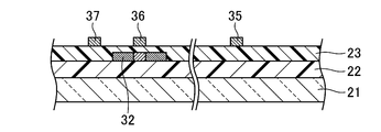
- FIG. 5 is a cross-sectional view showing a glass substrate on which a second active layer is formed.
- FIG. 6 is a cross-sectional view showing a glass substrate on which a plurality of gate electrodes are formed.
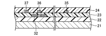
- FIG. 7 is a cross-sectional view showing a glass substrate on which an interlayer insulating film is formed.
- FIG. 1 is a cross-sectional view showing the structure of the TFT substrate according to the first embodiment.
- FIG. 2 is a plan view showing the CMOS inverter circuit according to the first embodiment.
- FIG. 3 is a circuit diagram showing a
- FIG. 8 is a cross-sectional view showing a glass substrate on which a source electrode and a drain electrode are formed.
- FIG. 9 is a cross-sectional view illustrating a glass substrate on which a plurality of oxide semiconductor layers are formed.
- FIG. 10 is a cross-sectional view showing the structure of the TFT substrate according to the second embodiment.
- FIG. 11 is a plan view showing a CMOS inverter circuit according to the second embodiment.
- FIG. 12 is a cross-sectional view showing a glass substrate on which a plurality of gate electrodes are formed.
- FIG. 13 is a cross-sectional view illustrating a glass substrate on which a plurality of oxide semiconductor layers are formed.
- FIG. 14 is a cross-sectional view showing the structure of the TFT substrate according to the third embodiment.
- FIG. 15 is a cross-sectional view showing a schematic configuration of a cross section taken along line XV-XV in FIG.
- FIG. 16 is a plan view showing a CMOS inverter circuit according to the third embodiment.
- FIG. 17 is a cross-sectional view showing a glass substrate on which a plurality of gate electrodes are formed.
- FIG. 18 is a cross-sectional view illustrating a glass substrate on which a plurality of oxide semiconductor layers are formed.
- Embodiment 1 of the Invention 1 to 9 show Embodiment 1 of the present invention.
- FIG. 1 is a cross-sectional view showing the structure of the TFT substrate according to the first embodiment.
- FIG. 2 is a plan view showing the CMOS inverter circuit according to the first embodiment.
- FIG. 3 is a circuit diagram showing a configuration of the CMOS inverter circuit.
- FIG. 4 is a cross-sectional view illustrating a schematic configuration of the liquid crystal display device.
- FIG. 5 is a cross-sectional view showing a glass substrate on which a second active layer is formed.
- FIG. 6 is a cross-sectional view showing a glass substrate on which a plurality of gate electrodes are formed.
- FIG. 7 is a cross-sectional view showing a glass substrate on which an interlayer insulating film is formed.
- FIG. 8 is a cross-sectional view showing a glass substrate on which a source electrode and a drain electrode are formed.
- FIG. 9 is a cross-sectional view illustrating a glass substrate on which a plurality of oxide semiconductor layers are formed.
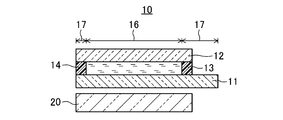
- the liquid crystal display device 1 will be described as an example of the display device according to the present invention.
- the liquid crystal display device 1 includes a liquid crystal display panel 10 and a backlight unit 20 that is a lighting device disposed on the back side of the liquid crystal display panel 10.
- the liquid crystal display panel 10 includes a TFT substrate 11 as an active matrix substrate which is a circuit substrate, a counter substrate 12 disposed to face the TFT substrate 11, and a liquid crystal layer provided between the TFT substrate 11 and the counter substrate 12. 13.
- the liquid crystal display panel 10 and the TFT substrate 11 are provided with a display region 16 and a frame-like non-display region 17 provided on the outer periphery.
- a display region 16 a plurality of pixels (not shown) arranged in a matrix are formed.
- the pixel displays for example, one of the three primary colors of red (R), green (G), and blue (B), and color display of an arbitrary color is performed by a pixel unit composed of a set of R, G, and B pixels. It is like that.
- the counter substrate 12 is provided with a color filter, a common electrode, etc. (not shown). Further, the liquid crystal layer 13 is sealed by a sealing member 14 provided between the TFT substrate 11 and the counter substrate 12.
- a plurality of source wirings (not shown) extending in parallel with each other and a plurality of gate wirings (not shown) extending orthogonally to these are formed on the TFT substrate 11. That is, the wiring group composed of the gate wiring and the source wiring is formed in a lattice shape as a whole. The pixels are formed in the lattice area.
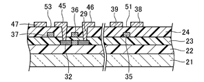
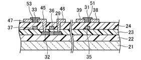
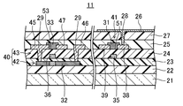
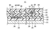
- a pixel driving TFT 41 for driving the pixel for each pixel and a pixel electrode 26 connected thereto are formed on the glass substrate 21.
- the pixel driving TFT 41 is connected to the source wiring and the gate wiring.
- a driving circuit TFT 42 for driving the pixel driving TFT 41 is formed directly on the glass substrate 21.
- the pixel driving TFT 41 is an n-channel TFT and has a first active layer 31 made of an oxide semiconductor such as IGZO.
- the drive circuit TFT 42 is a p-channel TFT, and has a second active layer 32 made of a non-oxide semiconductor such as low-temperature polysilicon (LTPS).
- LTPS low-temperature polysilicon
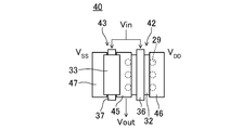
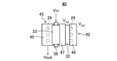
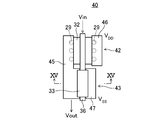
- CMOS inverter circuit 40 as a CMOS circuit is directly formed on the glass substrate 21 in the non-display area 17 of the TFT substrate 11.
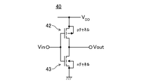
- the CMOS inverter circuit 40 includes a p-channel TFT 42 constituted by the drive circuit TFT 42 and an n-channel TFT 43 that shakes the third active layer 33 made of an oxide semiconductor such as IGZO. And have.
- the same signal voltage Vin is input to the gate electrode 36 of the p-channel TFT 42 and the gate electrode 37 of the n-channel TFT 43 simultaneously.
- a positive power supply VDD is connected to the source electrode 46 of the p-channel TFT 42, while the source electrode 47 of the n-channel TFT 43 is electrically grounded.
- the p-channel TFT 42 and the n-channel TFT 43 have a common drain electrode 45, and a signal voltage Vout is output from the drain electrode 45.
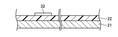
- the TFT substrate 11 has a glass substrate 21 as a transparent insulating substrate.
- a base coat layer 22 is formed on one surface of the glass substrate 21.
- the base coat layer 22 is an insulating film made of, for example, a SiO 2 film, a SiNx film, or a laminated structure including a SiO 2 film and a SiNx film.
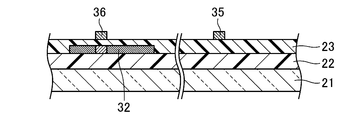
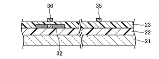
- a second active layer 32 made of low-temperature polysilicon is formed in a predetermined shape on the surface of the base coat layer 22 in the non-display region 17.
- a gate insulating film 23 is formed on the base coat layer 22 so as to cover the second active layer 32.
- the gate insulating film 23 is made of, for example, a SiO 2 film.
- gate electrodes 35, 36, and 37 constituting the TFTs 41, 42, and 43 are formed on the surface of the gate insulating film 23. That is, the pixel driving TFT 41 and the driving circuit TFT 42 have gate electrodes 35 and 36 formed in the same layer. As shown in FIG. 2, the gate electrode 36 of the p-channel TFT 42 extends in parallel with the gate electrode 37 of the n-channel TFT 43. An interlayer insulating film 24 is formed on the gate insulating film 23 so as to cover the gate electrodes 35, 36 and 37.
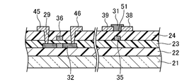
- Source electrodes 39, 46, 47 and drain electrodes 38, 45 are formed on the surface of the interlayer insulating film 24.
- the source electrode 46 and the drain electrode 45 are connected to the second active layer 32 through a contact hole 29 formed in the interlayer insulating film 24 and the gate insulating film 23.
- the pixel driving TFT 41 and the n-channel TFT 43 of the CMOS inverter circuit 40 have source electrodes 39 and 47 and drain electrodes 38 and 45 that are spaced apart from each other on the interlayer insulating film 24.
- a separation portion 51 is formed between the source electrode 39 and the drain electrode 38, and a separation portion 53 is formed between the source electrode 47 and the drain electrode 45.
- the first active layer 31 made of an oxide semiconductor is provided so as to cover the separation part 51, a part of the source electrode 39 adjacent to the separation part 51 and a part of the drain electrode 38 from the side opposite to the interlayer insulating film 24. Is provided. Similarly, a third portion made of an oxide semiconductor covers the separation portion 53 and a part of the source electrode 47 and a part of the drain electrode 45 adjacent to the separation portion 53 from the side opposite to the interlayer insulating film 24. An active layer 33 is provided.
- the n-channel TFT 43 of the CMOS inverter circuit 40 includes the source electrode 47, the drain electrode 45, and the third active layer having the same positional relationship as the source electrode 39, the drain electrode 38, and the first active layer 31 in the pixel driving TFT 41.
- a layer 33 is provided.
- the second active layer 32 of the p-channel TFT 42 and the third active layer 33 of the n-channel TFT 43 in the CMOS inverter circuit 40 are formed on the surface of the TFT substrate 11. They are arranged so as not to overlap each other when viewed from the normal direction.
- a passivation film 25 is formed on the surface of the interlayer insulating film 24 so as to cover the first active layer 31, the third active layer 33, the source electrodes 39, 46, 47 and the drain electrodes 38, 45. Further, a planarizing film 27 is formed on the surface of the passivation film 25.
- the planarizing film 27 is composed of a photosensitive insulating film.
- a pixel electrode 26 made of a transparent conductive film such as ITO is formed on the surface of the planarizing film 27. The pixel electrode 26 is connected to the drain electrode 38 of the pixel driving TFT 41 through a contact hole 28 formed in the planarizing film 27 and the passivation film 25.
- an amorphous silicon (hereinafter also referred to as a-Si) film is formed on the surface of the base coat layer 22 formed on the glass substrate 21 by, for example, PCVD (Plasma Chemical Vapor Deposition). Form to thickness.
- a-Si amorphous silicon
- the a-Si film is crystallized by light irradiation using an excimer laser to form a polysilicon (poly-Si) film (excimer laser annealing method).
- a resist layer is formed on the polysilicon film, and the polysilicon film is etched using the resist layer as a patterning mask, whereby the island-shaped semiconductor layer 32 is formed in the non-display region 17.
- a gate insulating film 23 is formed so as to cover the semiconductor layer 32.
- the gate insulating film 23 is formed of a SiO 2 film having a thickness of 50 nm to 100 nm, for example. Thereafter, impurities are implanted into the entire semiconductor layer 32 as necessary.
- gate electrodes 35, 36 and 37 are formed on the surface of the gate insulating film 23.
- a conductive film deposited on the surface of the gate insulating film 23 by sputtering or CVD is patterned into a predetermined shape by photolithography or the like.
- the gate electrode 36 is formed so as to cover a region to be a channel region in the semiconductor layer 32.
- the gate electrode 35 of the pixel driving TFT 41, the gate electrode 36 of the p-channel TFT 42, which is the driving circuit TFT 42, and the gate electrode 37 of the n-channel TFT 43 are formed in the same layer. Further, the gate electrode 36 of the p-channel TFT 42 is formed so as to extend in parallel with the gate electrode 37 of the n-channel TFT 43.
- the p-channel TFT 42 and the channel TFT 43 constitute a CMOS inverter circuit 40.
- impurity ions such as boron ions are implanted into the semiconductor layer 32 using the gate electrode 36 as a mask, and an activation process is performed by heating.
- impurity ions such as boron ions are implanted into the semiconductor layer 32 using the gate electrode 36 as a mask, and an activation process is performed by heating.
- the p-channel TFT 42 is formed, and the second active layer 32 made of a non-oxide semiconductor is formed in the non-display region 17 of the TFT substrate 11. It forms in the area which becomes.
- the gate insulating film 23 and the gate are formed over the entire glass substrate 21 (that is, over the region serving as the display region 16 and the region serving as the non-display region 17 of the TFT substrate 11).
- An interlayer insulating film 24 is formed so as to cover the electrodes 35, 36 and 37.
- a contact hole 29 is formed at a position above the second active layer 32 in the interlayer insulating film 24 and the gate insulating film 23.
- the conductive film formed on the interlayer insulating film 24 is patterned by photolithography or the like, thereby forming the source electrodes 39, 46, 47 and the drain electrodes 38, 45.
- the source electrode 46 and the drain electrode 45 are connected to the second active layer 32 through the contact hole 29, respectively.
- the source electrode 39 and the drain electrode 38 constituting the pixel driving TFT 41 are formed on the interlayer insulating film 24 in a state of being separated from each other.
- the source electrode 47 and the drain electrode 45 of the n-channel TFT 43 are formed on the interlayer insulating film 24 so as to be separated from each other.
- an oxide semiconductor film having a film thickness of, for example, about 30 nm to 100 nm is formed by sputtering so as to directly cover the source electrodes 39, 46, 47 and the drain electrodes 38, 45.
- etching using photolithography and a resist mask on the oxide semiconductor film, as illustrated in FIG.
- the third active layer 33 is made of the same oxide semiconductor as the first active layer 31.
- the first active layer 31 is formed in a region that becomes the display region 16 of the TFT substrate 11.
- the third active layer 33 is formed in a region to be the non-display region 17 of the TFT substrate 11. In this step, the third active layer 33 is formed so as not to overlap the second active layer 32 when viewed from the normal direction of the surface of the TFT substrate 11.
- the pixel driving TFT 41 and the n-channel TFT 43 in which the first active layer 31 or the third active layer 33 of the oxide semiconductor is disposed on the opposite side can be formed on the same glass substrate 21.
- a passivation film 25 is formed so as to cover the first active layer 31 and the third active layer 33, and then a planarizing film 27 is formed on the surface of the passivation film 25. Thereafter, a contact hole 28 is formed in the passivation film 25 and the planarizing film 27 at a position above the drain electrode 38 in the pixel driving TFT 41. Subsequently, the pixel electrode 26 is formed by patterning a transparent conductive film such as ITO deposited on the surface of the planarizing film 27 into a predetermined shape by photolithography.
- an alignment film (not shown) is formed so as to cover the pixel electrode 26, and the TFT substrate 11 is manufactured. Then, the TFT substrate 11 and the separately formed counter substrate 12 are bonded to each other via the liquid crystal layer 13 and the frame-shaped sealing member 14 to manufacture the liquid crystal display panel 10. Further, the backlight unit 20 is disposed opposite to the TFT substrate 11 side of the liquid crystal display panel 10 to manufacture the liquid crystal display device 1.
- the first active layer 31 of the pixel driving TFT 41 in the display region 16 is configured by an oxide semiconductor such as IGZO, the off-leak current of the pixel driving TFT 41 can be significantly reduced. It is not necessary to add another circuit function, and the aperture ratio can be greatly increased. Furthermore, since the second active layer 32 of the driving circuit TFT (n-channel TFT) 42 in the non-display region 17 is made of low-temperature polysilicon, which is a non-oxide semiconductor, the threshold voltage is lowered to drive at high speed. Is possible.
- the CMOS inverter circuit 40 and the pixel driving TFT 41 which are peripheral circuits, are integrally formed on the glass substrate 21, and the off-leakage current of the pixel driving TFT 41 is greatly increased while improving the reliability of the driving circuit TFT 42. It can be reduced.
- the source electrode 39 and the drain electrode 38 of the pixel driving TFT 41 are partially covered by the first active layer 31 from the side opposite to the interlayer insulating film 24 where the source electrode 39 and the drain electrode 38 are disposed. Therefore, it is not necessary to form an etching stopper layer on the first active layer 31.
- the third active layer 33 is covered from a part of the source electrode 47 and the drain electrode 45 of the n-channel TFT 43 of the CMOS inverter circuit 40 from the side opposite to the interlayer insulating film 24. It is not necessary to provide an etching stopper layer also on the layer 33.
- CMOS inverter circuit 40 can be configured.
- the active layer is made of low-temperature polysilicon as in the prior art, it is necessary to form an LDD (Lighty Doped Dorain) structure in order to operate at high speed. There is a problem that the manufacturing process increases.
- the third active layer 33 is formed of an oxide semiconductor for the n-channel TFT 43 constituting the CMOS inverter circuit 40, the manufacturing process of the CMOS inverter circuit 40 is reduced. However, the operation can be speeded up.
- an n-channel TFT and a p-channel TFT constituting the circuit each have an active layer made of a non-oxide semiconductor such as low-temperature polysilicon (LTPS). Yes.
- the active layers are arranged next to each other in the same layer.
- the third active layer 33 of the n-channel TFT 43 is not overlapped with the second active layer 32 of the p-channel TFT 42 when viewed from the normal direction of the surface of the TFT substrate 11.
- the CMOS inverter circuit 40 can be formed with the same occupation area as a CMOS inverter circuit having an n-channel TFT and a p-channel TFT each having an active layer made of LTPS.
- Embodiment 2 of the Invention >> 10 to 13 show Embodiment 2 of the present invention.
- FIG. 10 is a cross-sectional view showing the structure of the TFT substrate according to the second embodiment.
- FIG. 11 is a plan view showing a CMOS inverter circuit according to the second embodiment.
- FIG. 12 is a cross-sectional view showing a glass substrate on which a plurality of gate electrodes are formed.
- FIG. 13 is a cross-sectional view illustrating a glass substrate on which a plurality of oxide semiconductor layers are formed.
- the second embodiment is obtained by changing the configuration of the CMOS inverter circuit 40 in the first embodiment. That is, in the first embodiment, the third active layer 33 of the n-channel TFT 43 is disposed so as not to overlap the second active layer 32 of the p-channel TFT 42 when viewed from the normal direction of the surface of the TFT substrate 11. On the other hand, in the second embodiment, as shown in FIG. 10, the third active layer 33 is disposed so as to overlap the second active layer 32 when viewed from the normal direction of the surface of the TFT substrate 11.
- the p-channel TFT 42 and the n-channel TFT 43 have a common gate electrode 36.
- the TFT substrate 11 has a glass substrate 21 as a transparent insulating substrate.
- a base coat layer 22 is formed on one surface of the glass substrate 21.
- a second active layer 32 made of low-temperature polysilicon is formed in a predetermined shape on the surface of the base coat layer 22 in the non-display region 17.
- a gate insulating film 23 is formed on the base coat layer 22 so as to cover the second active layer 32.
- the gate insulating film 23 is made of, for example, a SiO 2 film.
- gate electrodes 35 and 36 constituting the TFTs 41, 42 and 43 are formed on the surface of the gate insulating film 23. That is, the pixel driving TFT 41 and the driving circuit TFT 42 have gate electrodes 35 and 36 formed in the same layer. As shown in FIGS. 10 and 11, the gate electrode 36 of the p-channel TFT 42 is the same as the gate electrode 36 of the n-channel TFT 43.
- An interlayer insulating film 24 is formed on the gate insulating film 23 so as to cover the gate electrodes 35 and 36.
- Source electrodes 39, 46, 47 and drain electrodes 38, 45 are formed on the surface of the interlayer insulating film 24.
- the source electrode 46 and the drain electrode 45 are connected to the second active layer 32 through a contact hole 29 formed in the interlayer insulating film 24 and the gate insulating film 23.
- the pixel driving TFT 41 and the n-channel TFT 43 of the CMOS inverter circuit 40 have source electrodes 39 and 47 and drain electrodes 38 and 45 that are spaced apart from each other on the interlayer insulating film 24.
- a separation portion 51 is formed between the source electrode 39 and the drain electrode 38, and a separation portion 53 is formed between the source electrode 47 and the drain electrode 45.
- the first active layer 31 made of an oxide semiconductor is provided so as to cover the separation part 51, a part of the source electrode 39 adjacent to the separation part 51 and a part of the drain electrode 38 from the side opposite to the interlayer insulating film 24. Is provided. Similarly, a third portion made of an oxide semiconductor covers the separation portion 53 and a part of the source electrode 47 and a part of the drain electrode 45 adjacent to the separation portion 53 from the side opposite to the interlayer insulating film 24. An active layer 33 is provided.
- a passivation film 25 is formed on the surface of the interlayer insulating film 24 so as to cover the first active layer 31, the third active layer 33, the source electrodes 39, 46, 47 and the drain electrodes 38, 45. Further, a planarizing film 27 is formed on the surface of the passivation film 25. A pixel electrode 26 made of a transparent conductive film such as ITO is formed on the surface of the planarizing film 27. The pixel electrode 26 is connected to the drain electrode 38 of the pixel driving TFT 41 through a contact hole 28 formed in the planarizing film 27 and the passivation film 25.
- a-Si film for example, is formed on the surface of the base coat layer 22 formed on the glass substrate 21 to a thickness of, for example, about 50 nm by PCVD or the like. To do. Subsequently, a polysilicon film is formed from the a-Si film by excimer laser annealing. Next, the island-shaped semiconductor layer 32 is formed in the non-display region 17 by etching the polysilicon film.
- the gate insulating film 23 is formed so as to cover the semiconductor layer 32.
- the gate insulating film 23 is formed of a SiO 2 film having a thickness of 50 nm to 100 nm, for example.
- impurities are implanted into the entire semiconductor layer 32 as necessary.
- the gate electrodes 35 and 36 are formed by patterning the conductive film deposited on the surface of the gate insulating film 23 by a sputtering method or a CVD method into a predetermined shape by photolithography or the like.
- the gate electrode 36 is a gate electrode common to the p-channel TFT 42 and the n-channel TFT 43.
- impurity ions such as boron ions are implanted into the semiconductor layer 32 using the gate electrode 36 as a mask, and an activation process is performed by heating, whereby the second active layer 32 is formed.
- the interlayer insulating film 24 is formed so as to cover the gate insulating film 23 and the gate electrodes 35 and 36 over the entire glass substrate 21. Subsequently, a contact hole 29 is formed above the second active layer 32 in the interlayer insulating film 24 and the gate insulating film 23. Thereafter, the conductive film formed on the interlayer insulating film 24 is patterned by photolithography or the like, thereby forming the source electrodes 39, 46, 47 and the drain electrodes 38, 45.
- the source electrode 46 and the drain electrode 45 are connected to the second active layer 32 through the contact holes 29, respectively.
- an oxide semiconductor film having a film thickness of, for example, about 30 nm to 100 nm is formed by sputtering so as to directly cover the source electrodes 39, 46, 47 and the drain electrodes 38, 45.
- the oxide semiconductor film is etched using photolithography and a resist mask, so that the island-shaped first active layer 31 and the first active layer 31 covering the separation portions 51 and 53 are formed as shown in FIG. Three active layers 33 are formed.
- the third active layer 33 is formed so as to overlap the second active layer 32 when viewed from the normal direction of the surface of the TFT substrate 11.
- a passivation film 25 is formed so as to cover the first active layer 31 and the third active layer 33, and then a planarizing film 27 is formed on the surface of the passivation film 25. Thereafter, a contact hole 28 is formed in the passivation film 25 and the planarizing film 27 at a position above the drain electrode 38 in the pixel driving TFT 41. Subsequently, the pixel electrode 26 is formed by patterning a transparent conductive film such as ITO deposited on the surface of the planarizing film 27 into a predetermined shape by photolithography. In this way, the TFT substrate 11 is manufactured.
- a transparent conductive film such as ITO
- the first active layer 31 is made of an oxide semiconductor such as IGZO as in the first embodiment. Therefore, the off-leak current of the pixel driving TFT 41 can be greatly reduced, and the aperture ratio can be reduced. Can greatly increase. Furthermore, since the second active layer 32 of the driving circuit TFT (n-channel TFT) 42 is made of low-temperature polysilicon, it can be driven at a high speed by lowering its threshold voltage. Therefore, the CMOS inverter circuit 40 and the pixel driving TFT 41, which are peripheral circuits, are integrally formed on the glass substrate 21, and the off-leakage current of the pixel driving TFT 41 is greatly increased while improving the reliability of the driving circuit TFT 42. It can be reduced.
- each of the source electrode 39 and the drain electrode 38 of the pixel driving TFT 41 is covered with the first active layer 31 from the side opposite to the interlayer insulating film 24 where the source electrode 39 and the drain electrode 38 are disposed. Since each of the source electrode 47 and the drain electrode 45 of the n-channel TFT 43 of the CMOS inverter circuit 40 covers the third active layer 33 from the side opposite to the interlayer insulating film 24, the first active layer 31 and There is no need to form an etching stopper layer on each of the third active layers 33.
- the third active layer 33 is formed of an oxide semiconductor for the n-channel TFT 43 constituting the CMOS inverter circuit 40, compared to the conventional configuration having an active layer of low-temperature polysilicon having an LDD structure.
- the operation of the CMOS inverter circuit 40 can be speeded up while reducing the number of manufacturing steps.
- the third active layer 33 of the n-channel TFT 43 is viewed from the normal direction of the surface of the TFT substrate 11 with the second active layer 32 of the p-channel TFT 42. Since they are arranged in an overlapping manner, the CMOS inverter circuit 40 can be miniaturized by reducing the area occupied by the layers.
- Embodiment 3 of the Invention >> 14 to 18 show Embodiment 3 of the present invention.
- FIG. 14 is a cross-sectional view showing the structure of the TFT substrate according to the third embodiment.
- FIG. 15 is a cross-sectional view showing a schematic configuration of a cross section taken along line XV-XV in FIG.
- FIG. 16 is a plan view showing a CMOS inverter circuit according to the third embodiment.
- FIG. 17 is a cross-sectional view showing a glass substrate on which a plurality of gate electrodes are formed.
- FIG. 18 is a cross-sectional view illustrating a glass substrate on which a plurality of oxide semiconductor layers are formed.
- the configuration of the CMOS inverter circuit 40 in the first embodiment is changed. That is, the third embodiment is that the third active layer 33 of the n-channel TFT 43 does not overlap the second active layer 32 of the p-channel TFT 42 when viewed from the normal direction of the surface of the TFT substrate 11. Same as 1.
- the gate electrodes 36 and 37 of the CMOS inverter circuit 40 are formed so as to extend in parallel with each other.
- the gate electrode 36 of the p-channel TFT 42 is an n-channel. This is different in that the gate electrode 36 of the type TFT 43 is connected to each other and extends linearly.
- the TFT substrate 11 has a glass substrate 21 as a transparent insulating substrate.
- a base coat layer 22 is formed on one surface of the glass substrate 21.
- a second active layer 32 made of low-temperature polysilicon is formed in a predetermined shape on the surface of the base coat layer 22 in the non-display region 17.
- a gate insulating film 23 is formed on the base coat layer 22 so as to cover the second active layer 32.
- the gate insulating film 23 is made of, for example, a SiO 2 film.
- gate electrodes 35 and 36 constituting the TFTs 41, 42 and 43 are formed on the surface of the gate insulating film 23. That is, the pixel driving TFT 41 and the driving circuit TFT 42 have gate electrodes 35 and 36 formed in the same layer. As shown in FIGS. 14 to 16, the gate electrode 36 of the p-channel TFT 42 is shared with the gate electrode 36 of the n-channel TFT 43. An interlayer insulating film 24 is formed on the gate insulating film 23 so as to cover the gate electrodes 35 and 36.
- Source electrodes 39, 46, 47 and drain electrodes 38, 45 are formed on the surface of the interlayer insulating film 24.
- the source electrode 46 and the drain electrode 45 are connected to the second active layer 32 through a contact hole 29 formed in the interlayer insulating film 24 and the gate insulating film 23.
- the pixel driving TFT 41 and the n-channel TFT 43 of the CMOS inverter circuit 40 have source electrodes 39 and 47 and drain electrodes 38 and 45 that are spaced apart from each other on the interlayer insulating film 24.
- a separation portion 51 is formed between the source electrode 39 and the drain electrode 38, and a separation portion (not shown) is also formed between the source electrode 47 and the drain electrode 45.
- the first active layer 31 made of an oxide semiconductor is provided so as to cover the separation part 51, a part of the source electrode 39 adjacent to the separation part 51 and a part of the drain electrode 38 from the side opposite to the interlayer insulating film 24. Is provided. Similarly, a separation part between the source electrode 47 and the drain electrode 45 and a part of the source electrode 47 and a part of the drain electrode 45 adjacent to the separation part are covered from the side opposite to the interlayer insulating film 24.
- a third active layer 33 made of an oxide semiconductor is provided.
- the third active layer 33 is arranged to be shifted from each other in the direction in which the gate electrode 36 extends with respect to the second active layer 32 when viewed from the normal direction of the surface of the TFT substrate 11, and does not overlap each other.
- a passivation film 25 is formed on the surface of the interlayer insulating film 24 so as to cover the first active layer 31, the third active layer 33, the source electrodes 39, 46, 47 and the drain electrodes 38, 45. Further, a planarizing film 27 is formed on the surface of the passivation film 25. A pixel electrode 26 made of a transparent conductive film such as ITO is formed on the surface of the planarizing film 27. The pixel electrode 26 is connected to the drain electrode 38 of the pixel driving TFT 41 through a contact hole 28 formed in the planarizing film 27 and the passivation film 25.
- an a-Si film for example, is formed on the surface of the base coat layer 22 formed on the glass substrate 21 to a thickness of, for example, about 50 nm by PCVD or the like. To do. Subsequently, a polysilicon film is formed from the a-Si film by excimer laser annealing. Next, the island-shaped semiconductor layer 32 is formed in the non-display region 17 by etching the polysilicon film.
- the gate insulating film 23 is formed so as to cover the semiconductor layer 32.
- the gate insulating film 23 is formed of a SiO 2 film having a thickness of 50 nm to 100 nm, for example. Thereafter, impurities are implanted into the entire semiconductor layer 32 as necessary.
- the gate electrodes 35 and 36 are formed by patterning the conductive film deposited on the surface of the gate insulating film 23 by a sputtering method or a CVD method into a predetermined shape by photolithography or the like.
- the gate electrode 36 of the p-channel TFT 42 is connected to the gate electrode 37 of the n-channel TFT 43 so as to extend linearly.
- impurity ions such as boron ions are implanted into the semiconductor layer 32 using the gate electrode 36 as a mask, and an activation process by heating is performed, thereby forming the second active layer 32.
- the interlayer insulating film 24 is formed so as to cover the gate insulating film 23 and the gate electrodes 35 and 36 over the entire glass substrate 21. Subsequently, a contact hole 29 is formed above the second active layer 32 in the interlayer insulating film 24 and the gate insulating film 23. Thereafter, the conductive film formed on the interlayer insulating film 24 is patterned by photolithography or the like, thereby forming the source electrodes 39, 46, 47 and the drain electrodes 38, 45. Thus, the source electrode 46 and the drain electrode 45 are connected to the second active layer 32 through the contact holes 29, respectively.
- an oxide semiconductor film having a film thickness of, for example, about 30 nm to 100 nm is formed by sputtering so as to directly cover the source electrodes 39, 46, 47 and the drain electrodes 38, 45.
- this oxide semiconductor film is etched using photolithography and a resist mask to cover the separation portion 51 or the separation portion between the source electrode 47 and the drain electrode 45 as shown in FIG.
- An island-shaped first active layer 31 and a third active layer 33 are formed.
- a passivation film 25 is formed so as to cover the first active layer 31 and the third active layer 33, and then a planarizing film 27 is formed on the surface of the passivation film 25. Thereafter, a contact hole 28 is formed in the passivation film 25 and the planarizing film 27 at a position above the drain electrode 38 in the pixel driving TFT 41. Subsequently, the pixel electrode 26 is formed by patterning a transparent conductive film such as ITO deposited on the surface of the planarizing film 27 into a predetermined shape by photolithography. In this way, the TFT substrate 11 is manufactured.
- a transparent conductive film such as ITO
- the first active layer 31 is formed of an oxide semiconductor such as IGZO
- the off-leak current of the pixel driving TFT 41 can be greatly reduced, and the aperture ratio can be reduced. Can greatly increase.
- the second active layer 32 of the driving circuit TFT (n-channel TFT) 42 is made of low-temperature polysilicon, it can be driven at a high speed by lowering its threshold voltage. Therefore, the CMOS inverter circuit 40 and the pixel driving TFT 41, which are peripheral circuits, are integrally formed on the glass substrate 21, and the off-leakage current of the pixel driving TFT 41 is greatly increased while improving the reliability of the driving circuit TFT 42. It can be reduced.
- each of the source electrode 39 and the drain electrode 38 of the pixel driving TFT 41 is covered with the first active layer 31 from the side opposite to the interlayer insulating film 24 where the source electrode 39 and the drain electrode 38 are disposed. Since each of the source electrode 47 and the drain electrode 45 of the n-channel TFT 43 of the CMOS inverter circuit 40 covers the third active layer 33 from the side opposite to the interlayer insulating film 24, the first active layer 31 and There is no need to form an etching stopper layer on each of the third active layers 33.
- the third active layer 33 is formed of an oxide semiconductor for the n-channel TFT 43 constituting the CMOS inverter circuit 40, compared to the conventional configuration having an active layer of low-temperature polysilicon having an LDD structure.
- the operation of the CMOS inverter circuit 40 can be speeded up while reducing the number of manufacturing steps.
- the display device having the CMOS inverter circuit 40 has been described.
- the present invention is not limited to this, and for example, a NAND circuit, an AND circuit, a NOR circuit, an OR circuit, a shift register circuit, a sampling circuit, The present invention can be similarly applied to a display device having another CMOS circuit having a D / A converter circuit, an A / D converter circuit, a latch circuit, a buffer circuit, or the like.
- ZnO InGaO 3 (ZnO) 5 , MgxZn 1-x O (magnesium zinc oxide), CdZn 1-x O (cadmium zinc oxide), CdO (cadmium oxide), or a- And IGZO (In—Ga—Zn—O-based amorphous oxide semiconductor).
- ZnO doped with one or more kinds of impurity elements among group 1 element, group 13 element, group 14 element, group 15 element and group 17 element is in an amorphous state, a polycrystalline state or a non-crystalline state. It is also possible to use a microcrystalline state in which a crystalline state and a polycrystalline state are mixed, or a state in which no impurity element is added.
- non-oxide semiconductor may be a semiconductor such as silicon other than low-temperature polysilicon.
- the present invention has been described with respect to the liquid crystal display device, but the present invention can be similarly applied to other display devices such as an organic EL display device.
- the present invention is not limited to the above-described first to third embodiments, and the present invention includes a configuration in which these first to third embodiments are appropriately combined.
- the present invention is useful for a display device including a thin film transistor having an oxide semiconductor layer and a manufacturing method thereof.
- Liquid crystal display device 11 TFT substrate (circuit board) 16 display area 17 Non-display area 21 Glass substrate 31 First active layer 32 Second active layer, semiconductor layer 33 Third active layer 35, 36, 37 Gate electrode 38, 45 Drain electrode 39, 46, 47 Source electrode 40 CMOS inverter circuit 41 Pixel drive TFT 42 p-channel TFT (TFT for drive circuit) 43 n-channel TFT 45 Drain electrode 51,53 remote part
Landscapes
- Thin Film Transistor (AREA)
- Liquid Crystal (AREA)
- Devices For Indicating Variable Information By Combining Individual Elements (AREA)
Priority Applications (6)
| Application Number | Priority Date | Filing Date | Title |
|---|---|---|---|
| JP2013521441A JP6215053B2 (ja) | 2011-06-24 | 2012-06-18 | 表示装置及びその製造方法 |
| SG2014013833A SG2014013833A (en) | 2011-06-24 | 2012-06-18 | Display device and method for manufacturing same |
| CN201280041110.1A CN103765494B (zh) | 2011-06-24 | 2012-06-18 | 显示装置及其制造方法 |
| US14/128,437 US10177170B2 (en) | 2011-06-24 | 2012-06-18 | Display device and method for manufacturing same |
| CA2845768A CA2845768A1 (en) | 2011-06-24 | 2012-06-18 | Display device and method for manufacturing same |
| US16/203,732 US10438973B2 (en) | 2011-06-24 | 2018-11-29 | Display device and method for manufacturing same |
Applications Claiming Priority (2)
| Application Number | Priority Date | Filing Date | Title |
|---|---|---|---|
| JP2011140300 | 2011-06-24 | ||
| JP2011-140300 | 2011-06-24 |
Related Child Applications (2)
| Application Number | Title | Priority Date | Filing Date |
|---|---|---|---|
| US14/128,437 A-371-Of-International US10177170B2 (en) | 2011-06-24 | 2012-06-18 | Display device and method for manufacturing same |
| US16/203,732 Division US10438973B2 (en) | 2011-06-24 | 2018-11-29 | Display device and method for manufacturing same |
Publications (1)
| Publication Number | Publication Date |
|---|---|
| WO2012176422A1 true WO2012176422A1 (ja) | 2012-12-27 |
Family
ID=47422280
Family Applications (1)
| Application Number | Title | Priority Date | Filing Date |
|---|---|---|---|
| PCT/JP2012/003960 WO2012176422A1 (ja) | 2011-06-24 | 2012-06-18 | 表示装置及びその製造方法 |
Country Status (6)
Cited By (29)
| Publication number | Priority date | Publication date | Assignee | Title |
|---|---|---|---|---|
| CN103730485A (zh) * | 2013-12-27 | 2014-04-16 | 京东方科技集团股份有限公司 | 双面显示的oled阵列基板及其制备方法、显示装置 |
| WO2015052991A1 (ja) * | 2013-10-09 | 2015-04-16 | シャープ株式会社 | 半導体装置およびその製造方法 |
| KR20150101416A (ko) * | 2014-02-24 | 2015-09-03 | 엘지디스플레이 주식회사 | 박막 트랜지스터 기판 및 이를 이용한 표시장치 |
| KR20150101417A (ko) * | 2014-02-24 | 2015-09-03 | 엘지디스플레이 주식회사 | 표시장치 |
| US9129927B2 (en) | 2013-08-26 | 2015-09-08 | Apple Inc. | Organic light-emitting diode displays with semiconducting-oxide and silicon thin-film transistors |
| JP2015179838A (ja) * | 2014-02-28 | 2015-10-08 | 株式会社半導体エネルギー研究所 | 半導体装置 |
| JP2015188077A (ja) * | 2014-03-13 | 2015-10-29 | 株式会社半導体エネルギー研究所 | 撮像装置 |
| JP2015194577A (ja) * | 2014-03-31 | 2015-11-05 | ソニー株式会社 | 表示装置および電子機器 |
| KR20160018825A (ko) * | 2013-08-26 | 2016-02-17 | 애플 인크. | 실리콘 및 반도체성 산화물 박막 트랜지스터를 구비한 디스플레이 |
| JP2016086164A (ja) * | 2014-10-24 | 2016-05-19 | 株式会社半導体エネルギー研究所 | 撮像装置および電子機器 |
| KR20160103494A (ko) * | 2015-10-07 | 2016-09-01 | 엘지디스플레이 주식회사 | 박막 트랜지스터 기판 및 이를 이용한 표시장치 |
| KR20160103492A (ko) * | 2015-10-07 | 2016-09-01 | 엘지디스플레이 주식회사 | 박막 트랜지스터 기판 및 이를 이용한 표시장치 |
| KR20160103495A (ko) * | 2015-10-07 | 2016-09-01 | 엘지디스플레이 주식회사 | 박막 트랜지스터 기판 및 이를 이용한 표시장치 |
| JP2017510979A (ja) * | 2014-03-27 | 2017-04-13 | インテル・コーポレーション | マルチデバイスのフレキシブルエレクトロニクスシステムオンチップ(soc)のプロセス統合 |
| KR20170051296A (ko) * | 2015-10-30 | 2017-05-11 | 가부시키가이샤 한도오따이 에네루기 켄큐쇼 | 반도체 장치 및 전자 기기 |
| WO2017130776A1 (ja) * | 2016-01-27 | 2017-08-03 | シャープ株式会社 | 半導体装置およびその製造方法 |
| JP2017201665A (ja) * | 2016-05-06 | 2017-11-09 | 株式会社ジャパンディスプレイ | 表示装置 |
| JP2017227832A (ja) * | 2016-06-24 | 2017-12-28 | 株式会社ジャパンディスプレイ | 表示装置 |
| JP2018036290A (ja) * | 2016-08-29 | 2018-03-08 | 株式会社ジャパンディスプレイ | 表示装置 |
| WO2018043426A1 (ja) * | 2016-09-05 | 2018-03-08 | シャープ株式会社 | アクティブマトリクス基板およびその製造方法 |
| JP2018049227A (ja) * | 2016-09-23 | 2018-03-29 | 株式会社半導体エネルギー研究所 | 表示装置および電子機器 |
| JP2018093082A (ja) * | 2016-12-05 | 2018-06-14 | 株式会社Joled | 半導体装置、半導体装置の製造方法および表示装置 |
| KR20180073659A (ko) * | 2015-12-04 | 2018-07-02 | 애플 인크. | 발광 다이오드를 갖는 디스플레이 |
| US10032841B2 (en) | 2014-09-24 | 2018-07-24 | Apple Inc. | Silicon and semiconducting oxide thin-film transistor displays |
| WO2018179121A1 (ja) * | 2017-03-29 | 2018-10-04 | シャープ株式会社 | 半導体装置および半導体装置の製造方法 |
| US10211235B2 (en) | 2016-09-14 | 2019-02-19 | Japan Display Inc. | Display device and manufacturing method thereof |
| JP2020205402A (ja) * | 2019-06-14 | 2020-12-24 | Tianma Japan株式会社 | 薄膜デバイス |
| WO2024166389A1 (ja) * | 2023-02-10 | 2024-08-15 | シャープディスプレイテクノロジー株式会社 | 表示装置 |
| US12414378B2 (en) | 2023-12-08 | 2025-09-09 | Apple Inc. | Displays with silicon and semiconducting oxide thin-film transistors |
Families Citing this family (41)
| Publication number | Priority date | Publication date | Assignee | Title |
|---|---|---|---|---|
| US8354674B2 (en) * | 2007-06-29 | 2013-01-15 | Semiconductor Energy Laboratory Co., Ltd. | Semiconductor device wherein a property of a first semiconductor layer is different from a property of a second semiconductor layer |
| US8969154B2 (en) * | 2011-08-23 | 2015-03-03 | Micron Technology, Inc. | Methods for fabricating semiconductor device structures and arrays of vertical transistor devices |
| US9228717B2 (en) * | 2013-11-28 | 2016-01-05 | Lg Display Co., Ltd. | Quantum rod compound including electron acceptor and quantum rod luminescent display device including the same |
| EP2911195B1 (en) | 2014-02-24 | 2020-05-27 | LG Display Co., Ltd. | Thin film transistor substrate and display using the same |
| US9881986B2 (en) | 2014-02-24 | 2018-01-30 | Lg Display Co., Ltd. | Thin film transistor substrate and display using the same |
| US10186528B2 (en) | 2014-02-24 | 2019-01-22 | Lg Display Co., Ltd. | Thin film transistor substrate and display using the same |
| US10325937B2 (en) | 2014-02-24 | 2019-06-18 | Lg Display Co., Ltd. | Thin film transistor substrate with intermediate insulating layer and display using the same |
| US9214508B2 (en) | 2014-02-24 | 2015-12-15 | Lg Display Co., Ltd. | Thin film transistor substrate with intermediate insulating layer and display using the same |
| US10985196B2 (en) | 2014-02-24 | 2021-04-20 | Lg Display Co., Ltd. | Thin film transistor substrate with intermediate insulating layer and display using the same |
| EP2911202B1 (en) | 2014-02-24 | 2019-02-20 | LG Display Co., Ltd. | Thin film transistor substrate and display using the same |
| EP2911199B1 (en) | 2014-02-24 | 2020-05-06 | LG Display Co., Ltd. | Thin film transistor substrate and display using the same |
| US9490276B2 (en) * | 2014-02-25 | 2016-11-08 | Lg Display Co., Ltd. | Display backplane and method of fabricating the same |
| US9634038B2 (en) * | 2014-02-25 | 2017-04-25 | Lg Display Co., Ltd. | Display backplane having multiple types of thin-film-transistors |
| CN104377167B (zh) * | 2014-11-13 | 2017-04-05 | 京东方科技集团股份有限公司 | 薄膜晶体管阵列基板及其制作方法、显示面板和显示装置 |
| CN104409514A (zh) * | 2014-11-21 | 2015-03-11 | 京东方科技集团股份有限公司 | 一种薄膜晶体管结构、其制作方法及相关装置 |
| CN104538401B (zh) * | 2014-12-23 | 2017-05-03 | 深圳市华星光电技术有限公司 | Tft基板结构 |
| KR102785340B1 (ko) * | 2014-12-31 | 2025-03-20 | 엘지디스플레이 주식회사 | 다수의 타입들의 박막 트랜지스터들을 갖는 디스플레이 백플레인 |
| KR20250109240A (ko) * | 2014-12-31 | 2025-07-16 | 엘지디스플레이 주식회사 | 다수의 타입들의 박막 트랜지스터들을 갖는 디스플레이 백플레인 |
| KR101658716B1 (ko) * | 2014-12-31 | 2016-09-30 | 엘지디스플레이 주식회사 | 표시 장치 |
| US9685469B2 (en) * | 2015-04-03 | 2017-06-20 | Apple Inc. | Display with semiconducting oxide and polysilicon transistors |
| TW201704831A (zh) * | 2015-07-31 | 2017-02-01 | 凌巨科技股份有限公司 | 薄膜電晶體結構 |
| US20170294454A1 (en) * | 2015-10-29 | 2017-10-12 | Boe Technology Group Co., Ltd | Array substrate and fabricating method thereof, display panel, and display apparatus |
| KR102519942B1 (ko) * | 2015-11-26 | 2023-04-11 | 엘지디스플레이 주식회사 | 유기발광 다이오드 표시장치용 박막 트랜지스터 기판 |
| CN105552085B (zh) * | 2015-12-25 | 2019-04-30 | 昆山国显光电有限公司 | 一种像素驱动电路及其制备方法 |
| US10510781B2 (en) * | 2016-02-22 | 2019-12-17 | Sharp Kabushiki Kaisha | Semiconductor device and method for manufacturing semiconductor device |
| JP6673731B2 (ja) | 2016-03-23 | 2020-03-25 | 株式会社ジャパンディスプレイ | 表示装置及びその製造方法 |
| US10468434B2 (en) * | 2016-04-08 | 2019-11-05 | Innolux Corporation | Hybrid thin film transistor structure, display device, and method of making the same |
| TWI579926B (zh) * | 2016-05-25 | 2017-04-21 | 友達光電股份有限公司 | 主動元件陣列基板 |
| KR102458660B1 (ko) | 2016-08-03 | 2022-10-26 | 가부시키가이샤 한도오따이 에네루기 켄큐쇼 | 표시 장치 및 전자 기기 |
| KR102731378B1 (ko) * | 2016-08-31 | 2024-11-15 | 엘지디스플레이 주식회사 | 멀티 타입의 박막 트랜지스터를 포함하는 유기 발광 표시 장치 및 유기 발광 표시 장치 제조 방법 |
| KR102541552B1 (ko) | 2016-11-30 | 2023-06-07 | 엘지디스플레이 주식회사 | 트랜지스터 기판 및 이를 이용한 유기발광표시패널과 유기발광표시장치 |
| KR102733082B1 (ko) * | 2016-12-30 | 2024-11-22 | 엘지디스플레이 주식회사 | 구동 박막 트랜지스터 및 이를 이용한 유기 발광 표시 장치 |
| KR102736793B1 (ko) | 2017-01-05 | 2024-12-04 | 삼성디스플레이 주식회사 | 주사 구동부 및 이를 포함하는 표시 장치 |
| CN106952928B (zh) * | 2017-03-30 | 2018-10-23 | 深圳市华星光电技术有限公司 | 一种tft背板的制作方法及tft背板 |
| CN107026178B (zh) * | 2017-04-28 | 2019-03-15 | 深圳市华星光电技术有限公司 | 一种阵列基板、显示装置及其制作方法 |
| JP7250558B2 (ja) | 2019-02-19 | 2023-04-03 | 株式会社ジャパンディスプレイ | 表示装置及び半導体装置 |
| WO2020184533A1 (ja) | 2019-03-11 | 2020-09-17 | 株式会社ジャパンディスプレイ | 表示装置及び半導体装置 |
| CN110289269A (zh) * | 2019-06-26 | 2019-09-27 | 上海天马微电子有限公司 | 一种阵列基板、显示面板和显示装置 |
| CN111081719A (zh) * | 2019-12-12 | 2020-04-28 | 武汉华星光电半导体显示技术有限公司 | 一种阵列基板及其制造方法 |
| CN111179742A (zh) * | 2020-02-12 | 2020-05-19 | 武汉华星光电技术有限公司 | 一种显示面板、栅极驱动电路及电子装置 |
| CN113192986B (zh) * | 2021-04-27 | 2023-01-10 | 深圳市华星光电半导体显示技术有限公司 | 显示面板及其制备方法 |
Citations (4)
| Publication number | Priority date | Publication date | Assignee | Title |
|---|---|---|---|---|
| JP2010003910A (ja) * | 2008-06-20 | 2010-01-07 | Toshiba Mobile Display Co Ltd | 表示素子 |
| JP2010045243A (ja) * | 2008-08-14 | 2010-02-25 | Fujifilm Corp | 薄膜電界効果型トランジスタ及びその製造方法 |
| JP2010074148A (ja) * | 2008-08-20 | 2010-04-02 | Ricoh Co Ltd | 電界効果型トランジスタ、表示素子、画像表示装置及びシステム |
| JP2010135772A (ja) * | 2008-11-07 | 2010-06-17 | Semiconductor Energy Lab Co Ltd | 半導体装置及び当該半導体装置の作製方法 |
Family Cites Families (15)
| Publication number | Priority date | Publication date | Assignee | Title |
|---|---|---|---|---|
| JP2653099B2 (ja) * | 1988-05-17 | 1997-09-10 | セイコーエプソン株式会社 | アクティブマトリクスパネル,投写型表示装置及びビューファインダー |
| US5274279A (en) * | 1988-05-17 | 1993-12-28 | Seiko Epson Corporation | Thin film CMOS inverter |
| JPH1184418A (ja) | 1997-09-08 | 1999-03-26 | Sanyo Electric Co Ltd | 表示装置 |
| JPH11274512A (ja) * | 1998-03-26 | 1999-10-08 | Toshiba Corp | 薄膜トランジスタ装置 |
| JP2000155313A (ja) * | 2000-01-01 | 2000-06-06 | Semiconductor Energy Lab Co Ltd | アクティブマトリクス型液晶表示装置 |
| JP4275336B2 (ja) | 2001-11-16 | 2009-06-10 | 株式会社半導体エネルギー研究所 | 半導体装置の作製方法 |
| KR100583972B1 (ko) * | 2004-11-26 | 2006-05-26 | 삼성전자주식회사 | 씨모스 인버터의 노드 콘택 구조체를 갖는 반도체소자의제조방법들 |
| JP5060738B2 (ja) | 2006-04-28 | 2012-10-31 | 株式会社ジャパンディスプレイイースト | 画像表示装置 |
| TWI585498B (zh) * | 2006-05-16 | 2017-06-01 | 半導體能源研究所股份有限公司 | 液晶顯示裝置和半導體裝置 |
| CN101356652B (zh) * | 2006-06-02 | 2012-04-18 | 日本财团法人高知县产业振兴中心 | 包括由氧化锌构成的氧化物半导体薄膜层的半导体器件及其制造方法 |
| KR101100999B1 (ko) * | 2009-01-13 | 2011-12-29 | 삼성모바일디스플레이주식회사 | 씨모스 박막트랜지스터 및 그 제조방법과 이를 구비한 유기전계발광 표시장치 |
| TWI430441B (zh) * | 2009-04-07 | 2014-03-11 | Innolux Corp | 影像顯示系統及其製造方法 |
| KR101782176B1 (ko) * | 2009-07-18 | 2017-09-26 | 가부시키가이샤 한도오따이 에네루기 켄큐쇼 | 반도체 장치 및 반도체 장치의 제조 방법 |
| KR101073542B1 (ko) * | 2009-09-03 | 2011-10-17 | 삼성모바일디스플레이주식회사 | 유기 발광 표시 장치 및 그 제조 방법 |
| KR101343293B1 (ko) * | 2010-04-30 | 2013-12-18 | 샤프 가부시키가이샤 | 회로 기판 및 표시 장치 |
-
2012
- 2012-06-18 CN CN201280041110.1A patent/CN103765494B/zh active Active
- 2012-06-18 JP JP2013521441A patent/JP6215053B2/ja active Active
- 2012-06-18 WO PCT/JP2012/003960 patent/WO2012176422A1/ja active Application Filing
- 2012-06-18 CA CA2845768A patent/CA2845768A1/en not_active Abandoned
- 2012-06-18 SG SG10201605237SA patent/SG10201605237SA/en unknown
- 2012-06-18 SG SG2014013833A patent/SG2014013833A/en unknown
- 2012-06-18 US US14/128,437 patent/US10177170B2/en active Active
-
2016
- 2016-06-16 JP JP2016120053A patent/JP2016194703A/ja active Pending
-
2018
- 2018-11-29 US US16/203,732 patent/US10438973B2/en active Active
Patent Citations (4)
| Publication number | Priority date | Publication date | Assignee | Title |
|---|---|---|---|---|
| JP2010003910A (ja) * | 2008-06-20 | 2010-01-07 | Toshiba Mobile Display Co Ltd | 表示素子 |
| JP2010045243A (ja) * | 2008-08-14 | 2010-02-25 | Fujifilm Corp | 薄膜電界効果型トランジスタ及びその製造方法 |
| JP2010074148A (ja) * | 2008-08-20 | 2010-04-02 | Ricoh Co Ltd | 電界効果型トランジスタ、表示素子、画像表示装置及びシステム |
| JP2010135772A (ja) * | 2008-11-07 | 2010-06-17 | Semiconductor Energy Lab Co Ltd | 半導体装置及び当該半導体装置の作製方法 |
Cited By (83)
| Publication number | Priority date | Publication date | Assignee | Title |
|---|---|---|---|---|
| KR101794856B1 (ko) * | 2013-08-26 | 2017-11-07 | 애플 인크. | 실리콘 및 반도체성 산화물 박막 트랜지스터를 구비한 디스플레이 |
| US11876099B2 (en) | 2013-08-26 | 2024-01-16 | Apple Inc. | Displays with silicon and semiconducting oxide thin-film transistors |
| US11587954B2 (en) | 2013-08-26 | 2023-02-21 | Apple Inc. | Displays with silicon and semiconducting oxide thin-film transistors |
| US11177291B2 (en) | 2013-08-26 | 2021-11-16 | Apple Inc. | Displays with silicon and semiconducting oxide thin-film transistors |
| US9129927B2 (en) | 2013-08-26 | 2015-09-08 | Apple Inc. | Organic light-emitting diode displays with semiconducting-oxide and silicon thin-film transistors |
| US10998344B2 (en) | 2013-08-26 | 2021-05-04 | Apple Inc. | Displays with silicon and semiconducting oxide thin-film transistors |
| US10741588B2 (en) | 2013-08-26 | 2020-08-11 | Apple Inc. | Displays with silicon and semiconducting oxide thin-film transistors |
| US10707237B2 (en) | 2013-08-26 | 2020-07-07 | Apple Inc. | Displays with silicon and semiconducting oxide thin-film transistors |
| KR20160018825A (ko) * | 2013-08-26 | 2016-02-17 | 애플 인크. | 실리콘 및 반도체성 산화물 박막 트랜지스터를 구비한 디스플레이 |
| CN105408813A (zh) * | 2013-08-26 | 2016-03-16 | 苹果公司 | 具有硅薄膜晶体管和半导体氧化物薄膜晶体管的显示器 |
| KR102015756B1 (ko) | 2013-08-26 | 2019-08-28 | 애플 인크. | 실리콘 및 반도체성 산화물 박막 트랜지스터를 구비한 디스플레이 |
| KR20190085175A (ko) * | 2013-08-26 | 2019-07-17 | 애플 인크. | 실리콘 및 반도체성 산화물 박막 트랜지스터를 구비한 디스플레이 |
| US9412799B2 (en) | 2013-08-26 | 2016-08-09 | Apple Inc. | Display driver circuitry for liquid crystal displays with semiconducting-oxide thin-film transistors |
| KR102001357B1 (ko) * | 2013-08-26 | 2019-07-17 | 애플 인크. | 실리콘 및 반도체성 산화물 박막 트랜지스터를 구비한 디스플레이 |
| US10096622B2 (en) | 2013-08-26 | 2018-10-09 | Apple Inc. | Displays with silicon and semiconducting oxide thin-film transistors |
| KR20180097782A (ko) * | 2013-08-26 | 2018-08-31 | 애플 인크. | 실리콘 및 반도체성 산화물 박막 트랜지스터를 구비한 디스플레이 |
| KR101892510B1 (ko) | 2013-08-26 | 2018-08-29 | 애플 인크. | 실리콘 및 반도체성 산화물 박막 트랜지스터를 구비한 디스플레이 |
| JP2016534390A (ja) * | 2013-08-26 | 2016-11-04 | アップル インコーポレイテッド | シリコン薄膜トランジスタ及び半導体酸化物薄膜トランジスタを有するディスプレイ |
| KR101700388B1 (ko) * | 2013-08-26 | 2017-01-26 | 애플 인크. | 실리콘 및 반도체성 산화물 박막 트랜지스터를 구비한 디스플레이 |
| US9564478B2 (en) | 2013-08-26 | 2017-02-07 | Apple Inc. | Liquid crystal displays with oxide-based thin-film transistors |
| KR20180015290A (ko) * | 2013-08-26 | 2018-02-12 | 애플 인크. | 실리콘 및 반도체성 산화물 박막 트랜지스터를 구비한 디스플레이 |
| KR101826209B1 (ko) * | 2013-08-26 | 2018-02-06 | 애플 인크. | 실리콘 및 반도체성 산화물 박막 트랜지스터를 구비한 디스플레이 |
| US9818765B2 (en) | 2013-08-26 | 2017-11-14 | Apple Inc. | Displays with silicon and semiconducting oxide thin-film transistors |
| JPWO2015052991A1 (ja) * | 2013-10-09 | 2017-03-09 | シャープ株式会社 | 半導体装置およびその製造方法 |
| TWI619258B (zh) * | 2013-10-09 | 2018-03-21 | 夏普股份有限公司 | 半導體裝置之製造方法 |
| CN105612608A (zh) * | 2013-10-09 | 2016-05-25 | 夏普株式会社 | 半导体装置及其制造方法 |
| US9985055B2 (en) | 2013-10-09 | 2018-05-29 | Sharp Kabushiki Kaisha | Semiconductor device and method for manufacturing same |
| WO2015052991A1 (ja) * | 2013-10-09 | 2015-04-16 | シャープ株式会社 | 半導体装置およびその製造方法 |
| TWI624952B (zh) * | 2013-10-09 | 2018-05-21 | 夏普股份有限公司 | 半導體裝置 |
| CN105612608B (zh) * | 2013-10-09 | 2019-12-20 | 夏普株式会社 | 半导体装置及其制造方法 |
| CN103730485A (zh) * | 2013-12-27 | 2014-04-16 | 京东方科技集团股份有限公司 | 双面显示的oled阵列基板及其制备方法、显示装置 |
| US9478595B2 (en) | 2013-12-27 | 2016-10-25 | Boe Technology Group Co., Ltd. | Double-sided display OLED array substrate, its manufacturing method, and display device |
| KR20150101417A (ko) * | 2014-02-24 | 2015-09-03 | 엘지디스플레이 주식회사 | 표시장치 |
| KR20150101416A (ko) * | 2014-02-24 | 2015-09-03 | 엘지디스플레이 주식회사 | 박막 트랜지스터 기판 및 이를 이용한 표시장치 |
| KR102454382B1 (ko) | 2014-02-24 | 2022-10-18 | 엘지디스플레이 주식회사 | 박막 트랜지스터 기판 및 이를 이용한 표시장치 |
| KR102401432B1 (ko) * | 2014-02-24 | 2022-05-26 | 엘지디스플레이 주식회사 | 표시장치 |
| JP7150123B2 (ja) | 2014-02-28 | 2022-10-07 | 株式会社半導体エネルギー研究所 | インバータ回路 |
| JP2021022748A (ja) * | 2014-02-28 | 2021-02-18 | 株式会社半導体エネルギー研究所 | 半導体装置 |
| JP2022017434A (ja) * | 2014-02-28 | 2022-01-25 | 株式会社半導体エネルギー研究所 | インバータ回路 |
| JP2015179838A (ja) * | 2014-02-28 | 2015-10-08 | 株式会社半導体エネルギー研究所 | 半導体装置 |
| JP2015188077A (ja) * | 2014-03-13 | 2015-10-29 | 株式会社半導体エネルギー研究所 | 撮像装置 |
| JP2017510979A (ja) * | 2014-03-27 | 2017-04-13 | インテル・コーポレーション | マルチデバイスのフレキシブルエレクトロニクスシステムオンチップ(soc)のプロセス統合 |
| JP2015194577A (ja) * | 2014-03-31 | 2015-11-05 | ソニー株式会社 | 表示装置および電子機器 |
| US10032841B2 (en) | 2014-09-24 | 2018-07-24 | Apple Inc. | Silicon and semiconducting oxide thin-film transistor displays |
| JP2024103708A (ja) * | 2014-10-24 | 2024-08-01 | 株式会社半導体エネルギー研究所 | 撮像装置及び電子機器 |
| JP7705984B2 (ja) | 2014-10-24 | 2025-07-10 | 株式会社半導体エネルギー研究所 | 撮像装置及び電子機器 |
| JP2016086164A (ja) * | 2014-10-24 | 2016-05-19 | 株式会社半導体エネルギー研究所 | 撮像装置および電子機器 |
| KR102178472B1 (ko) | 2015-10-07 | 2020-11-16 | 엘지디스플레이 주식회사 | 박막 트랜지스터 기판 및 이를 이용한 표시장치 |
| KR20160103492A (ko) * | 2015-10-07 | 2016-09-01 | 엘지디스플레이 주식회사 | 박막 트랜지스터 기판 및 이를 이용한 표시장치 |
| KR20160103494A (ko) * | 2015-10-07 | 2016-09-01 | 엘지디스플레이 주식회사 | 박막 트랜지스터 기판 및 이를 이용한 표시장치 |
| KR20160103495A (ko) * | 2015-10-07 | 2016-09-01 | 엘지디스플레이 주식회사 | 박막 트랜지스터 기판 및 이를 이용한 표시장치 |
| KR102179379B1 (ko) | 2015-10-07 | 2020-11-18 | 엘지디스플레이 주식회사 | 박막 트랜지스터 기판 및 이를 이용한 표시장치 |
| KR102179378B1 (ko) | 2015-10-07 | 2020-11-18 | 엘지디스플레이 주식회사 | 박막 트랜지스터 기판 및 이를 이용한 표시장치 |
| KR20170051296A (ko) * | 2015-10-30 | 2017-05-11 | 가부시키가이샤 한도오따이 에네루기 켄큐쇼 | 반도체 장치 및 전자 기기 |
| KR102623411B1 (ko) * | 2015-10-30 | 2024-01-11 | 가부시키가이샤 한도오따이 에네루기 켄큐쇼 | 반도체 장치 및 전자 기기 |
| US11870393B2 (en) | 2015-10-30 | 2024-01-09 | Semiconductor Energy Laboratory Co., Ltd. | Semiconductor device and electronic device each having oscillator |
| JP7033220B2 (ja) | 2015-10-30 | 2022-03-09 | 株式会社半導体エネルギー研究所 | 半導体装置 |
| JP2021077896A (ja) * | 2015-10-30 | 2021-05-20 | 株式会社半導体エネルギー研究所 | 半導体装置 |
| KR20180073659A (ko) * | 2015-12-04 | 2018-07-02 | 애플 인크. | 발광 다이오드를 갖는 디스플레이 |
| US11232748B2 (en) | 2015-12-04 | 2022-01-25 | Apple Inc. | Display with light-emitting diodes |
| KR102218493B1 (ko) * | 2015-12-04 | 2021-02-19 | 애플 인크. | 발광 다이오드를 갖는 디스플레이 |
| US10997917B2 (en) | 2015-12-04 | 2021-05-04 | Apple Inc. | Display with light-emitting diodes |
| US12142220B2 (en) | 2015-12-04 | 2024-11-12 | Apple Inc. | Display with light-emitting diodes |
| US10714009B2 (en) | 2015-12-04 | 2020-07-14 | Apple Inc. | Display with light-emitting diodes |
| KR20200001629A (ko) * | 2015-12-04 | 2020-01-06 | 애플 인크. | 발광 다이오드를 갖는 디스플레이 |
| US11615746B2 (en) | 2015-12-04 | 2023-03-28 | Apple Inc. | Display with light-emitting diodes |
| KR102179312B1 (ko) * | 2015-12-04 | 2020-11-16 | 애플 인크. | 발광 다이오드를 갖는 디스플레이 |
| US11875745B2 (en) | 2015-12-04 | 2024-01-16 | Apple Inc. | Display with light-emitting diodes |
| US11462163B2 (en) | 2015-12-04 | 2022-10-04 | Apple Inc. | Display with light-emitting diodes |
| WO2017130776A1 (ja) * | 2016-01-27 | 2017-08-03 | シャープ株式会社 | 半導体装置およびその製造方法 |
| JP2017201665A (ja) * | 2016-05-06 | 2017-11-09 | 株式会社ジャパンディスプレイ | 表示装置 |
| JP2017227832A (ja) * | 2016-06-24 | 2017-12-28 | 株式会社ジャパンディスプレイ | 表示装置 |
| JP2018036290A (ja) * | 2016-08-29 | 2018-03-08 | 株式会社ジャパンディスプレイ | 表示装置 |
| WO2018043426A1 (ja) * | 2016-09-05 | 2018-03-08 | シャープ株式会社 | アクティブマトリクス基板およびその製造方法 |
| US10211235B2 (en) | 2016-09-14 | 2019-02-19 | Japan Display Inc. | Display device and manufacturing method thereof |
| JP2018049227A (ja) * | 2016-09-23 | 2018-03-29 | 株式会社半導体エネルギー研究所 | 表示装置および電子機器 |
| JP2018093082A (ja) * | 2016-12-05 | 2018-06-14 | 株式会社Joled | 半導体装置、半導体装置の製造方法および表示装置 |
| US10840269B2 (en) | 2017-03-29 | 2020-11-17 | Sharp Kabushiki Kaisha | Semiconductor device and method of manufacturing semiconductor device |
| WO2018179121A1 (ja) * | 2017-03-29 | 2018-10-04 | シャープ株式会社 | 半導体装置および半導体装置の製造方法 |
| JP7464400B2 (ja) | 2019-06-14 | 2024-04-09 | Tianma Japan株式会社 | 薄膜デバイス |
| JP2020205402A (ja) * | 2019-06-14 | 2020-12-24 | Tianma Japan株式会社 | 薄膜デバイス |
| WO2024166389A1 (ja) * | 2023-02-10 | 2024-08-15 | シャープディスプレイテクノロジー株式会社 | 表示装置 |
| US12414378B2 (en) | 2023-12-08 | 2025-09-09 | Apple Inc. | Displays with silicon and semiconducting oxide thin-film transistors |
Also Published As
| Publication number | Publication date |
|---|---|
| CN103765494A (zh) | 2014-04-30 |
| SG2014013833A (en) | 2014-10-30 |
| US20140131703A1 (en) | 2014-05-15 |
| JP2016194703A (ja) | 2016-11-17 |
| US20190096922A1 (en) | 2019-03-28 |
| CA2845768A1 (en) | 2012-12-27 |
| US10438973B2 (en) | 2019-10-08 |
| SG10201605237SA (en) | 2016-08-30 |
| JPWO2012176422A1 (ja) | 2015-02-23 |
| JP6215053B2 (ja) | 2017-10-18 |
| CN103765494B (zh) | 2016-05-04 |
| US10177170B2 (en) | 2019-01-08 |
Similar Documents
| Publication | Publication Date | Title |
|---|---|---|
| JP6215053B2 (ja) | 表示装置及びその製造方法 | |
| JP7558219B2 (ja) | 発光表示装置 | |
| CN109273404B (zh) | 一种阵列基板及其制备方法、显示面板、显示装置 | |
| US10895774B2 (en) | Array substrate, manufacturing method, display panel and display device | |
| CN103081108B (zh) | 薄膜晶体管基板及其制造方法、显示装置 | |
| US8659092B2 (en) | Complementary metal oxide semiconductor transistor and fabricating method thereof | |
| CN105470197B (zh) | 低温多晶硅阵列基板的制作方法 | |
| WO2015194417A1 (ja) | 半導体装置 | |
| JP2011049529A (ja) | トランジスタ回路 | |
| CN104685635A (zh) | 半导体装置 | |
| CN103299429A (zh) | 有源矩阵基板及其制造方法以及显示面板 | |
| EP3168865A1 (en) | Array substrate manufacturing method | |
| JPWO2016157351A1 (ja) | 薄膜トランジスタ及び表示パネル | |
| US10825843B2 (en) | Active matrix substrate and method for producing same | |
| CN105470196A (zh) | 薄膜晶体管、阵列基板及其制造方法、和显示装置 | |
| US8842229B2 (en) | Thin film transistor substrate, method for producing same, and display device | |
| JP4669834B2 (ja) | 液晶表示装置の製造方法 | |
| WO2018090496A1 (zh) | 一种阵列基板及其制备方法、液晶显示面板 | |
| KR101338106B1 (ko) | 액정표시장치 및 그 제조방법 | |
| WO2017094644A1 (ja) | 半導体基板及び表示装置 | |
| CN105514126A (zh) | 一种阵列基板及其制作方法、显示装置 | |
| US20150325700A1 (en) | Thin film transistor and pixel structure | |
| CN111081719A (zh) | 一种阵列基板及其制造方法 | |
| KR101331803B1 (ko) | 액정표시장치 및 그 제조방법 | |
| JP2015181194A (ja) | トランジスタ回路 |
Legal Events
| Date | Code | Title | Description |
|---|---|---|---|
| WWE | Wipo information: entry into national phase |
Ref document number: 201280041110.1 Country of ref document: CN |
|
| 121 | Ep: the epo has been informed by wipo that ep was designated in this application |
Ref document number: 12803307 Country of ref document: EP Kind code of ref document: A1 |
|
| WWE | Wipo information: entry into national phase |
Ref document number: 14128437 Country of ref document: US |
|
| NENP | Non-entry into the national phase |
Ref country code: DE |
|
| ENP | Entry into the national phase |
Ref document number: 2845768 Country of ref document: CA |
|
| ENP | Entry into the national phase |
Ref document number: 2013521441 Country of ref document: JP Kind code of ref document: A |
|
| 122 | Ep: pct application non-entry in european phase |
Ref document number: 12803307 Country of ref document: EP Kind code of ref document: A1 |