WO2009119841A1 - Composition de polysiloxane durcissable, et produit durci en polysiloxane, élément optique, élément pour l’industrie aérospatiale, dispositif semi-conducteur émettant de la lumière, système d’éclairage, et dispositif d’affichage d’image utilisant la composition de polysiloxane durcissable - Google Patents
Composition de polysiloxane durcissable, et produit durci en polysiloxane, élément optique, élément pour l’industrie aérospatiale, dispositif semi-conducteur émettant de la lumière, système d’éclairage, et dispositif d’affichage d’image utilisant la composition de polysiloxane durcissable Download PDFInfo
- Publication number
- WO2009119841A1 WO2009119841A1 PCT/JP2009/056379 JP2009056379W WO2009119841A1 WO 2009119841 A1 WO2009119841 A1 WO 2009119841A1 JP 2009056379 W JP2009056379 W JP 2009056379W WO 2009119841 A1 WO2009119841 A1 WO 2009119841A1
- Authority
- WO
- WIPO (PCT)
- Prior art keywords
- light
- phosphor
- light emitting
- emitting device
- group
- Prior art date
Links
Images


Classifications
-
- C—CHEMISTRY; METALLURGY
- C08—ORGANIC MACROMOLECULAR COMPOUNDS; THEIR PREPARATION OR CHEMICAL WORKING-UP; COMPOSITIONS BASED THEREON
- C08L—COMPOSITIONS OF MACROMOLECULAR COMPOUNDS
- C08L83/00—Compositions of macromolecular compounds obtained by reactions forming in the main chain of the macromolecule a linkage containing silicon with or without sulfur, nitrogen, oxygen or carbon only; Compositions of derivatives of such polymers
- C08L83/04—Polysiloxanes
- C08L83/06—Polysiloxanes containing silicon bound to oxygen-containing groups
-
- H—ELECTRICITY
- H01—ELECTRIC ELEMENTS
- H01L—SEMICONDUCTOR DEVICES NOT COVERED BY CLASS H10
- H01L23/00—Details of semiconductor or other solid state devices
- H01L23/28—Encapsulations, e.g. encapsulating layers, coatings, e.g. for protection
- H01L23/29—Encapsulations, e.g. encapsulating layers, coatings, e.g. for protection characterised by the material, e.g. carbon
- H01L23/293—Organic, e.g. plastic
- H01L23/296—Organo-silicon compounds
-
- C—CHEMISTRY; METALLURGY
- C08—ORGANIC MACROMOLECULAR COMPOUNDS; THEIR PREPARATION OR CHEMICAL WORKING-UP; COMPOSITIONS BASED THEREON
- C08G—MACROMOLECULAR COMPOUNDS OBTAINED OTHERWISE THAN BY REACTIONS ONLY INVOLVING UNSATURATED CARBON-TO-CARBON BONDS
- C08G77/00—Macromolecular compounds obtained by reactions forming a linkage containing silicon with or without sulfur, nitrogen, oxygen or carbon in the main chain of the macromolecule
- C08G77/04—Polysiloxanes
- C08G77/12—Polysiloxanes containing silicon bound to hydrogen
-
- C—CHEMISTRY; METALLURGY
- C08—ORGANIC MACROMOLECULAR COMPOUNDS; THEIR PREPARATION OR CHEMICAL WORKING-UP; COMPOSITIONS BASED THEREON
- C08G—MACROMOLECULAR COMPOUNDS OBTAINED OTHERWISE THAN BY REACTIONS ONLY INVOLVING UNSATURATED CARBON-TO-CARBON BONDS
- C08G77/00—Macromolecular compounds obtained by reactions forming a linkage containing silicon with or without sulfur, nitrogen, oxygen or carbon in the main chain of the macromolecule
- C08G77/04—Polysiloxanes
- C08G77/14—Polysiloxanes containing silicon bound to oxygen-containing groups
- C08G77/16—Polysiloxanes containing silicon bound to oxygen-containing groups to hydroxyl groups
-
- C—CHEMISTRY; METALLURGY
- C08—ORGANIC MACROMOLECULAR COMPOUNDS; THEIR PREPARATION OR CHEMICAL WORKING-UP; COMPOSITIONS BASED THEREON
- C08G—MACROMOLECULAR COMPOUNDS OBTAINED OTHERWISE THAN BY REACTIONS ONLY INVOLVING UNSATURATED CARBON-TO-CARBON BONDS
- C08G77/00—Macromolecular compounds obtained by reactions forming a linkage containing silicon with or without sulfur, nitrogen, oxygen or carbon in the main chain of the macromolecule
- C08G77/04—Polysiloxanes
- C08G77/14—Polysiloxanes containing silicon bound to oxygen-containing groups
- C08G77/18—Polysiloxanes containing silicon bound to oxygen-containing groups to alkoxy or aryloxy groups
-
- C—CHEMISTRY; METALLURGY
- C08—ORGANIC MACROMOLECULAR COMPOUNDS; THEIR PREPARATION OR CHEMICAL WORKING-UP; COMPOSITIONS BASED THEREON
- C08G—MACROMOLECULAR COMPOUNDS OBTAINED OTHERWISE THAN BY REACTIONS ONLY INVOLVING UNSATURATED CARBON-TO-CARBON BONDS
- C08G77/00—Macromolecular compounds obtained by reactions forming a linkage containing silicon with or without sulfur, nitrogen, oxygen or carbon in the main chain of the macromolecule
- C08G77/04—Polysiloxanes
- C08G77/20—Polysiloxanes containing silicon bound to unsaturated aliphatic groups
-
- H—ELECTRICITY
- H01—ELECTRIC ELEMENTS
- H01L—SEMICONDUCTOR DEVICES NOT COVERED BY CLASS H10
- H01L2224/00—Indexing scheme for arrangements for connecting or disconnecting semiconductor or solid-state bodies and methods related thereto as covered by H01L24/00
- H01L2224/01—Means for bonding being attached to, or being formed on, the surface to be connected, e.g. chip-to-package, die-attach, "first-level" interconnects; Manufacturing methods related thereto
- H01L2224/42—Wire connectors; Manufacturing methods related thereto
- H01L2224/44—Structure, shape, material or disposition of the wire connectors prior to the connecting process
- H01L2224/45—Structure, shape, material or disposition of the wire connectors prior to the connecting process of an individual wire connector
- H01L2224/45001—Core members of the connector
- H01L2224/45099—Material
- H01L2224/451—Material with a principal constituent of the material being a metal or a metalloid, e.g. boron (B), silicon (Si), germanium (Ge), arsenic (As), antimony (Sb), tellurium (Te) and polonium (Po), and alloys thereof
- H01L2224/45138—Material with a principal constituent of the material being a metal or a metalloid, e.g. boron (B), silicon (Si), germanium (Ge), arsenic (As), antimony (Sb), tellurium (Te) and polonium (Po), and alloys thereof the principal constituent melting at a temperature of greater than or equal to 950°C and less than 1550°C
- H01L2224/45144—Gold (Au) as principal constituent
-
- H—ELECTRICITY
- H01—ELECTRIC ELEMENTS
- H01L—SEMICONDUCTOR DEVICES NOT COVERED BY CLASS H10
- H01L2224/00—Indexing scheme for arrangements for connecting or disconnecting semiconductor or solid-state bodies and methods related thereto as covered by H01L24/00
- H01L2224/01—Means for bonding being attached to, or being formed on, the surface to be connected, e.g. chip-to-package, die-attach, "first-level" interconnects; Manufacturing methods related thereto
- H01L2224/42—Wire connectors; Manufacturing methods related thereto
- H01L2224/47—Structure, shape, material or disposition of the wire connectors after the connecting process
- H01L2224/48—Structure, shape, material or disposition of the wire connectors after the connecting process of an individual wire connector
- H01L2224/4805—Shape
- H01L2224/4809—Loop shape
- H01L2224/48091—Arched
-
- H—ELECTRICITY
- H01—ELECTRIC ELEMENTS
- H01L—SEMICONDUCTOR DEVICES NOT COVERED BY CLASS H10
- H01L2224/00—Indexing scheme for arrangements for connecting or disconnecting semiconductor or solid-state bodies and methods related thereto as covered by H01L24/00
- H01L2224/01—Means for bonding being attached to, or being formed on, the surface to be connected, e.g. chip-to-package, die-attach, "first-level" interconnects; Manufacturing methods related thereto
- H01L2224/42—Wire connectors; Manufacturing methods related thereto
- H01L2224/47—Structure, shape, material or disposition of the wire connectors after the connecting process
- H01L2224/48—Structure, shape, material or disposition of the wire connectors after the connecting process of an individual wire connector
- H01L2224/481—Disposition
- H01L2224/48151—Connecting between a semiconductor or solid-state body and an item not being a semiconductor or solid-state body, e.g. chip-to-substrate, chip-to-passive
- H01L2224/48221—Connecting between a semiconductor or solid-state body and an item not being a semiconductor or solid-state body, e.g. chip-to-substrate, chip-to-passive the body and the item being stacked
- H01L2224/48225—Connecting between a semiconductor or solid-state body and an item not being a semiconductor or solid-state body, e.g. chip-to-substrate, chip-to-passive the body and the item being stacked the item being non-metallic, e.g. insulating substrate with or without metallisation
- H01L2224/48227—Connecting between a semiconductor or solid-state body and an item not being a semiconductor or solid-state body, e.g. chip-to-substrate, chip-to-passive the body and the item being stacked the item being non-metallic, e.g. insulating substrate with or without metallisation connecting the wire to a bond pad of the item
-
- H—ELECTRICITY
- H01—ELECTRIC ELEMENTS
- H01L—SEMICONDUCTOR DEVICES NOT COVERED BY CLASS H10
- H01L2224/00—Indexing scheme for arrangements for connecting or disconnecting semiconductor or solid-state bodies and methods related thereto as covered by H01L24/00
- H01L2224/01—Means for bonding being attached to, or being formed on, the surface to be connected, e.g. chip-to-package, die-attach, "first-level" interconnects; Manufacturing methods related thereto
- H01L2224/42—Wire connectors; Manufacturing methods related thereto
- H01L2224/47—Structure, shape, material or disposition of the wire connectors after the connecting process
- H01L2224/48—Structure, shape, material or disposition of the wire connectors after the connecting process of an individual wire connector
- H01L2224/481—Disposition
- H01L2224/48151—Connecting between a semiconductor or solid-state body and an item not being a semiconductor or solid-state body, e.g. chip-to-substrate, chip-to-passive
- H01L2224/48221—Connecting between a semiconductor or solid-state body and an item not being a semiconductor or solid-state body, e.g. chip-to-substrate, chip-to-passive the body and the item being stacked
- H01L2224/48245—Connecting between a semiconductor or solid-state body and an item not being a semiconductor or solid-state body, e.g. chip-to-substrate, chip-to-passive the body and the item being stacked the item being metallic
- H01L2224/48247—Connecting between a semiconductor or solid-state body and an item not being a semiconductor or solid-state body, e.g. chip-to-substrate, chip-to-passive the body and the item being stacked the item being metallic connecting the wire to a bond pad of the item
-
- H—ELECTRICITY
- H01—ELECTRIC ELEMENTS
- H01L—SEMICONDUCTOR DEVICES NOT COVERED BY CLASS H10
- H01L2224/00—Indexing scheme for arrangements for connecting or disconnecting semiconductor or solid-state bodies and methods related thereto as covered by H01L24/00
- H01L2224/01—Means for bonding being attached to, or being formed on, the surface to be connected, e.g. chip-to-package, die-attach, "first-level" interconnects; Manufacturing methods related thereto
- H01L2224/42—Wire connectors; Manufacturing methods related thereto
- H01L2224/47—Structure, shape, material or disposition of the wire connectors after the connecting process
- H01L2224/48—Structure, shape, material or disposition of the wire connectors after the connecting process of an individual wire connector
- H01L2224/481—Disposition
- H01L2224/48151—Connecting between a semiconductor or solid-state body and an item not being a semiconductor or solid-state body, e.g. chip-to-substrate, chip-to-passive
- H01L2224/48221—Connecting between a semiconductor or solid-state body and an item not being a semiconductor or solid-state body, e.g. chip-to-substrate, chip-to-passive the body and the item being stacked
- H01L2224/48245—Connecting between a semiconductor or solid-state body and an item not being a semiconductor or solid-state body, e.g. chip-to-substrate, chip-to-passive the body and the item being stacked the item being metallic
- H01L2224/48257—Connecting between a semiconductor or solid-state body and an item not being a semiconductor or solid-state body, e.g. chip-to-substrate, chip-to-passive the body and the item being stacked the item being metallic connecting the wire to a die pad of the item
-
- H—ELECTRICITY
- H01—ELECTRIC ELEMENTS
- H01L—SEMICONDUCTOR DEVICES NOT COVERED BY CLASS H10
- H01L2224/00—Indexing scheme for arrangements for connecting or disconnecting semiconductor or solid-state bodies and methods related thereto as covered by H01L24/00
- H01L2224/01—Means for bonding being attached to, or being formed on, the surface to be connected, e.g. chip-to-package, die-attach, "first-level" interconnects; Manufacturing methods related thereto
- H01L2224/42—Wire connectors; Manufacturing methods related thereto
- H01L2224/47—Structure, shape, material or disposition of the wire connectors after the connecting process
- H01L2224/49—Structure, shape, material or disposition of the wire connectors after the connecting process of a plurality of wire connectors
- H01L2224/491—Disposition
- H01L2224/49105—Connecting at different heights
- H01L2224/49107—Connecting at different heights on the semiconductor or solid-state body
-
- H—ELECTRICITY
- H01—ELECTRIC ELEMENTS
- H01L—SEMICONDUCTOR DEVICES NOT COVERED BY CLASS H10
- H01L2224/00—Indexing scheme for arrangements for connecting or disconnecting semiconductor or solid-state bodies and methods related thereto as covered by H01L24/00
- H01L2224/73—Means for bonding being of different types provided for in two or more of groups H01L2224/10, H01L2224/18, H01L2224/26, H01L2224/34, H01L2224/42, H01L2224/50, H01L2224/63, H01L2224/71
- H01L2224/732—Location after the connecting process
- H01L2224/73251—Location after the connecting process on different surfaces
- H01L2224/73265—Layer and wire connectors
-
- H—ELECTRICITY
- H01—ELECTRIC ELEMENTS
- H01L—SEMICONDUCTOR DEVICES NOT COVERED BY CLASS H10
- H01L2924/00—Indexing scheme for arrangements or methods for connecting or disconnecting semiconductor or solid-state bodies as covered by H01L24/00
- H01L2924/10—Details of semiconductor or other solid state devices to be connected
- H01L2924/11—Device type
- H01L2924/12—Passive devices, e.g. 2 terminal devices
- H01L2924/1204—Optical Diode
- H01L2924/12044—OLED
-
- H—ELECTRICITY
- H01—ELECTRIC ELEMENTS
- H01L—SEMICONDUCTOR DEVICES NOT COVERED BY CLASS H10
- H01L2924/00—Indexing scheme for arrangements or methods for connecting or disconnecting semiconductor or solid-state bodies as covered by H01L24/00
- H01L2924/15—Details of package parts other than the semiconductor or other solid state devices to be connected
- H01L2924/181—Encapsulation
-
- H—ELECTRICITY
- H01—ELECTRIC ELEMENTS
- H01L—SEMICONDUCTOR DEVICES NOT COVERED BY CLASS H10
- H01L2924/00—Indexing scheme for arrangements or methods for connecting or disconnecting semiconductor or solid-state bodies as covered by H01L24/00
- H01L2924/30—Technical effects
- H01L2924/301—Electrical effects
- H01L2924/3025—Electromagnetic shielding
Definitions
- the present invention relates to a novel curable polysiloxane composition, and a polysiloxane cured product, an optical member, an aerospace industry member, a semiconductor light emitting device, a lighting device, and an image display device using the same.
- a curable polysiloxane composition having excellent heat resistance, light resistance, film formability, adhesion, and low foamability, and a cured polysiloxane using the same, an optical member, a member for aerospace industry
- the present invention relates to a semiconductor light emitting device, a lighting device, and an image display device.
- the semiconductor light emitting element is a member such as a transparent resin (member for a semiconductor light emitting device). What is sealed with is generally used.
- an epoxy resin is used as the semiconductor light emitting device member.
- pigments such as fluorescent substance, in this epoxy resin etc.
- epoxy resin is highly hygroscopic, there are problems such as cracks caused by heat from the semiconductor light-emitting element that occurs when the semiconductor light-emitting device is used for a long time, and deterioration of the phosphor and light-emitting element due to the ingress of moisture. was there.
- the epoxy resin has deteriorated and colored with the shortening of the emission wavelength of the LED, so that there has been a problem that the luminance of the semiconductor light emitting device is remarkably lowered when used for a long time and at a high output. .
- silicone resins having excellent heat resistance and ultraviolet light resistance have been used as substitutes for epoxy resins. That is, semiconductor light emitting devices using a silicone resin (polysiloxane composition) as a material excellent in heat resistance and ultraviolet light resistance have been proposed (see, for example, Patent Documents 1 to 5).
- Patent Documents 1 to 4 describe curable resin compositions for sealing LED elements using specific organopolysiloxanes.
- the organopolysiloxanes described in Patent Documents 1 to 4 have improved film forming properties as compared with glass materials using only tetrafunctional silicon by adjusting the degree of crosslinking by introducing organic groups.
- the amount of trifunctional or higher functional silicon used as a crosslinking component is large, and the cured product is hard and brittle glass. For this reason, when applied to a large-sized semiconductor light emitting device such as a power LED, the stress cannot be relieved at the adhesive interface with the LED chip or reflector, and the sealant is liable to peel off during long-term lighting use or thermal shock such as reflow. .
- Patent Document 4 a specific member for a silicon-containing semiconductor light-emitting device that can solve the above-mentioned problems.
- semiconductor light emitting devices using short-wavelength LEDs in the near-ultraviolet to ultraviolet region tend to be deteriorated such as coloring
- when used for a semiconductor power device that further dissipates heat it has been desired to further increase the level of heat and hydrothermal stability while maintaining light resistance, film formability, and adhesion.
- heat stability is required to maintain the luminance of the phosphor even when used for a long time and at a high output.
- the polysiloxane composition of patent document 5 is a gel-like substance that can be used as a resin composition for sealing an LED element
- the gel-like substance does not stabilize its properties when the LED is lit and protects the light-emitting element.
- the purpose should be borne by the curable resin composition for sealing, it cannot be said to be suitable.
- the system is internally cured by a dehydrogenation type reaction, there is a decisive problem that foaming occurs due to the influence of by-produced hydrogen gas. Since this foaming causes the following problems, a means for solving this problem has been desired.
- the semiconductor light emitting device has excellent light resistance (particularly UV resistance) and adhesiveness, sufficient heat resistance and film formability, and does not cause cracking, peeling or coloring even after long-term use. Therefore, there has been a demand for an optical member that can be sealed with a high luminance retention rate when a phosphor is contained. Also, an optical member that can be used as a semiconductor light-emitting device with less foaming when cured as a sealing material, good light guiding properties and little deterioration, and can maintain a high luminance maintenance rate for a long time when containing a phosphor. was demanded.
- the present invention has been made in view of the above-described problems. That is, the object of the present invention is excellent in light resistance (particularly UV resistance) and adhesiveness, and has sufficient heat resistance, hydrothermal resistance and film-forming property, and has less foaming when cured and used for a long time.
- An object of the present invention is to provide a curable polysiloxane composition, and a member for aerospace industry, a semiconductor light-emitting device, a lighting device, and an image display device that take advantage of the excellent characteristics thereof.
- the inventors of the present invention are characterized by including two or more types of polysiloxane compounds having a specific structure and a dehydrogenative condensation reaction catalyst.
- the curable polysiloxane composition is excellent not only in light resistance but also in adhesiveness, and has extremely high heat resistance and hydrothermal resistance as compared with conventional ones.
- the present inventors have found that a member for a semiconductor light emitting device having a high luminance maintenance rate can be obtained when a body is contained, and the present invention has been completed.
- the semiconductor light-emitting device member forming liquid and the cured product thereof according to the present invention are not limited to the above-described semiconductor light-emitting device field, but also include light transmittance (transparency), light resistance, heat resistance, hydrothermal resistance, UV resistance, and the like. It has been found that the present invention has applicability to materials for aerospace industry and other materials that require various characteristics.
- the gist of the present invention resides in the following [1] to [19].
- [1] A siloxane compound containing two or more hydrosilyl groups in one molecule, A siloxane compound containing two or more silanol groups in one molecule, and Contains a dehydrogenative condensation reaction catalyst, In the following curing test, a curable polysiloxane composition having an average height of 0.12 cm or less.
- a polysiloxane compound represented by the following general formula (1), a polysiloxane compound represented by the following general formula (2) and containing two or more silanol groups in one molecule, and a dehydrogenative condensation reaction catalyst A curable polysiloxane composition comprising:
- R 13 to R 18 each independently represents a group selected from a hydrogen atom, an alkyl group, an alkenyl group, a hydroxyl group and an allyl group.
- p, q, and r represent an integer of 0 or more, and p + q + r ⁇ 1.
- R 19 is an alkenyl group
- R 20 is a monovalent hydrocarbon group having 6 or less carbon atoms or an alkoxy group having 3 or less carbon atoms, which may be the same or different.
- s and u are positive numbers, and t ⁇ 0, x ⁇ 0, and y ⁇ 0.
- the light transmittance at all wavelengths from 400 nm to 800 nm when the hardness measurement value (Shore A) by durometer type A is 5 or more and 90 or less and the film thickness is 1 mm is 80% or more.
- An optical member comprising the polysiloxane cured product according to [13] or [14].
- a member for aerospace industry comprising the polysiloxane cured product according to [13] or [14].
- a semiconductor light emitting device comprising the optical member according to [15].
- An illumination device comprising the semiconductor light emitting device according to [17].
- An image display device comprising the semiconductor light emitting device according to [17].
- the curable polysiloxane composition of the present invention is excellent in heat resistance, light resistance, hydrothermal resistance, and UV resistance, and foaming is further suppressed. Moreover, the polysiloxane hardened
- the optical member can be suitably used for a semiconductor light emitting device, a light guide plate, and a waveguide.
- the curable polysiloxane composition, the polysiloxane cured product, and the optical member of the present invention have high hydrothermal resistance, UV resistance, etc. in addition to the above-described characteristics, and therefore materials that require these various characteristics,
- the present invention can also be applied to device materials using semiconductor light emitting elements (ultraviolet to near ultraviolet LEDs) that emit light in the ultraviolet to near ultraviolet region, materials for aerospace industry, and other materials.
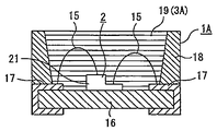
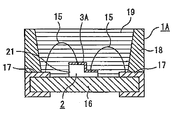
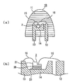
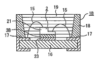
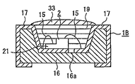
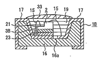
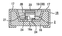
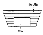
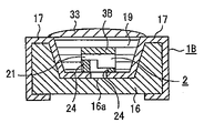
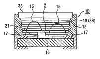
- FIG. 3 is a schematic sectional view showing Embodiment A-1. It is a schematic sectional drawing which shows embodiment A-2. Embodiment B-1 is shown, (a) is a schematic sectional view, and (b) is an enlarged view of the main part of (a). It is a schematic sectional drawing which shows Embodiment B-2. It is a schematic sectional drawing which shows Embodiment B-3.
- FIG. 10 is a schematic sectional view showing Embodiment B-4.
- FIG. 10 is a schematic sectional view showing Embodiment B-5.
- FIG. 10 is a schematic sectional view showing Embodiment B-6.
- FIG. 7 is a schematic sectional view showing Embodiment B-7.
- FIG. 10 is a schematic sectional view showing Embodiment B-8.
- FIG. 10 is a schematic sectional view showing Embodiment B-9.
- FIG. 10 is a schematic sectional view showing Embodiment B-10.
- FIG. 10 is a schematic sectional view showing Embodiment B-11.
- FIG. 13 is a schematic sectional view showing Embodiment B-12.
- FIG. 14 is a schematic sectional view showing Embodiment B-13.
- FIG. 15 is a schematic sectional view showing Embodiment B-14.
- FIG. 16 is a schematic sectional view showing Embodiment B-15.
- FIG. 16 is a schematic sectional view showing Embodiment B-16.
- FIG. 18 is a schematic sectional view showing Embodiment B-17.
- FIG. 19 is a schematic sectional view showing Embodiment B-18.
- FIG. 20 is a schematic sectional view showing Embodiment B-19.
- FIG. 21 is a schematic sectional view showing Embodiment B-20.
- FIG. 10 is a schematic sectional view showing Embodiment B-21.
- FIG. 22 is a cross-sectional view of a principal part showing Embodiment B-21.
- FIG. 22 is a schematic sectional view showing Embodiment B-22.
- FIG. 22 is a sectional view showing the principal parts of Embodiment B-22.
- FIG. 24 is a schematic sectional view showing Embodiment B-23.
- FIG. 25 is a perspective view of relevant parts showing Embodiment B-23.
- FIG. 25 is a schematic sectional view showing Embodiment B-24.
- FIG. 25 is a sectional view showing the principal parts of Embodiment B-24.
- FIG. 25 is a perspective view of relevant parts showing Embodiment B-24.
- FIG. 26 is a schematic sectional view showing Embodiment B-25.
- FIG. 26 is a schematic sectional view showing Embodiment B-26.
- FIG. 29 is a schematic sectional view showing Embodiment B-27.
- FIG. 29 is a schematic sectional view showing Embodiment B-28.
- FIG. 32 is a schematic sectional view showing Embodiment B-29.
- Embodiment B-30 is shown, (a) is a schematic sectional view, and (b) is an enlarged view of the main part of (a).
- FIG. 32 is a schematic sectional view showing Embodiment B-31.
- FIG. 32 is a schematic sectional view showing Embodiment B-32.
- FIG. 34 is a schematic sectional view showing Embodiment B-33.
- FIG. 36 is a schematic sectional view showing Embodiment B-34.
- FIG. 36 is a schematic sectional view showing Embodiment B-35.
- FIG. 36 is a schematic sectional view showing Embodiment B-36.
- FIG. 38 is a schematic sectional view showing Embodiment B-37.
- FIG. 39 is a schematic sectional view showing Embodiment B-38.
- FIG. 40 is a schematic sectional view showing Embodiment B-39.
- FIG. 40 is a schematic sectional view showing Embodiment B-40.
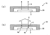
- FIG. 42 is a schematic sectional view showing Embodiment B-41. It is explanatory drawing of the other structural example of the principal part of each embodiment. (A), (b) is explanatory drawing of the basic concept of each embodiment.
- Curable polysiloxane composition One embodiment of the curable polysiloxane composition of the present invention contains a siloxane compound containing two or more hydrosilyl groups in one molecule and a siloxane compound containing two or more silanol groups in one molecule. It is characterized by. Another embodiment of the curable polysiloxane composition of the present invention contains a siloxane compound containing one or more hydrosilyl groups in one molecule and one or more silanol groups in one molecule. It is characterized by doing.
- a siloxane compound containing two or more hydrosilyl groups in one molecule is an organohydrogensilane or a linear, branched, three-dimensional network having at least two, preferably three or more SiH bonds in one molecule. It is an organohydrogenpolysiloxane. Of these, organohydrogenpolysiloxanes are preferred because they are less likely to volatilize during curing. As the substituent of the organohydrogenpolysiloxane, the following groups can be used, but those having no aliphatic unsaturated bond are preferable.
- the substituted or unsubstituted monovalent hydrocarbon group bonded to the silicon atom usually includes those having 1 to 12 carbon atoms, preferably about 1 to 8 carbon atoms.
- organohydrogensilane and organohydrogenpolysiloxane examples include (CH 3 ) SiH 3 , (CH 3 ) 2 SiH 2 , (C 6 H 5 ) SiH 3 , 1,1,3,3-tetramethyldisiloxane.
- the siloxane compound containing two or more silanol groups in one molecule acts as a crosslinking agent for curing the composition by the dehydrogenative condensation reaction with the hydrosilyl group-containing siloxane compound, and at least two in one molecule. It is a linear, branched, or three-dimensional net-like organopolysiloxane having the above silanol group.
- the substituent of this organopolysiloxane the same substituents as those of the above-mentioned organohydrogenpolysiloxane can be used, but those having no aliphatic unsaturated bond are preferred.
- a compound represented by the general formula (2) can be preferably used.
- a siloxane compound containing one or more hydrosilyl groups in one molecule and one or more silanol groups in one molecule is a siloxane compound containing two or more hydrosilyl groups in one molecule, and Linear, branched, and three-dimensional net-like organos that have the characteristics of a siloxane compound containing two or more silanol groups in one molecule, one or more hydrosilyl groups and one or more silanol groups in one molecule Polysiloxane.
- the substituent of this organopolysiloxane the same substituents as those of the above-mentioned organohydrogenpolysiloxane can be used, but those having no aliphatic unsaturated bond are preferred.
- Such compounds include, for example, dehydrogenative condensation or hydrolytic polycondensation of an organohydrogenpolysiloxane containing two or more hydrosilyl groups in one molecule and an organopolysiloxane containing two or more silanol groups in one molecule. It can be obtained by reacting by the method.
- the said manufacturing method is an example and a manufacturing method is not limited to this.
- One embodiment of the curable polysiloxane composition of the present invention is a polysiloxane compound represented by the following general formula (1), represented by the following general formula (2), and 2 silanol groups in one molecule. It is characterized by including a curing catalyst containing a polysiloxane compound containing at least one and a dehydrogenative condensation catalyst (preferably, metal, hydroxylamine or boron).
- a curing catalyst containing a polysiloxane compound containing at least one and a dehydrogenative condensation catalyst (preferably, metal, hydroxylamine or boron).
- R 1 to R 3 and R 5 to R 8 are each independently a group selected from a hydrogen atom, an alkyl group, an alkenyl group, an allyl group, and R 10 R 11 R 12 Si.
- R 4, R 9 ⁇ R 12 each independently represent a hydrogen atom, an alkyl group, a group selected from an alkenyl group and an allyl group.
- l represents an integer of 2 or more.
- m represents an integer of 0 or more.
- R 13 to R 18 each independently represents a group selected from a hydrogen atom, an alkyl group, an alkenyl group, and an allyl group.
- p, q, and r represent an integer of 0 or more, and p + q + r ⁇ 1.
- at least 80 mol% or more, preferably 95 mol% or more, more preferably 99 mol% or more is preferably a methyl group.
- the curable polysiloxane composition further includes a polysiloxane compound having an alkenyl group represented by the following general formula (3) or the like. Can do.
- R 19 is an alkenyl group
- R 20 is a monovalent hydrocarbon group having 6 or less carbon atoms and an alkoxy group having 3 or less carbon atoms, which may be the same or different, and is at least 80% or more, preferably 95 mol % Or more, more preferably 99 mol% or more is a methyl group.
- s and u are positive numbers, and t ⁇ 0, x ⁇ 0, and y ⁇ 0.
- Examples of the silicon-containing compound having an alkenyl group include vinyl group-containing polyorganosiloxanes which may be the same or different, and these are used singly or in combination of two or more in any ratio and combination. be able to. Among these, a vinyl group-containing polyorganosiloxane having two or more vinyl groups in the molecule is preferable.
- vinyl group-containing polyorganosiloxane having two or more vinyl groups in the molecule include both-end vinyl polydimethylsiloxane manufactured by Gelest: DMS-V00, DMS-V03, DMS-V05, DMS-V21, DMS-V22, DMS-V25, DMS-V31, DMS-V33, DMS-V35, DMS-V41, DMS-V42, DMS-V46, DMS-V52, Both end vinyldimethylsiloxane-diphenylsiloxane copolymer from Gelest: PDV-0325, PDV-0331, PDV-0341, PDV-0346, PDV-0525, PDV-0541, PDV-1625, PDV-1631, PDV-1635, PDV-1641, PDV-2331, PDV-2335, Both end vinylphenylmethylsiloxane from Gelest: PMV-9925, A trimethylsilyl-blocked vinylmethylsiloxane
- the curable polysiloxane composition of the present invention preferably contains a hydrosilyl group-containing polysiloxane compound represented by the following general formula (1).
- a hydrosilyl group in the siloxane skeleton By having a hydrosilyl group in the siloxane skeleton, the crosslinking density can be easily tuned.
- R 1 to R 3 and R 5 to R 8 are each independently a group selected from a hydrogen atom, an alkyl group, an alkenyl group, an allyl group, and R 10 R 11 R 12 Si.
- R 4, R 9 ⁇ R 12 each independently represent a hydrogen atom, an alkyl group, a group selected from an alkenyl group and an allyl group.
- l represents an integer of 2 or more.
- m represents an integer of 0 or more.
- R 1 to R 3 and R 5 to R 8 each independently represent a group selected from the group consisting of a hydrogen atom, an alkyl group, an alkenyl group, an allyl group, and R 10 R 11 R 12 Si.
- the alkyl group, alkenyl group, allyl group, and R 10 R 11 R 12 Si may be further substituted with a halogen atom.
- Preferred alkyl groups include, for example, a methyl group, an ethyl group, a propyl group, and a trifluoropropyl group.
- a preferable alkenyl group includes, for example, a vinyl group.
- a preferable allyl group includes, for example, a phenyl group. Among these, preferable examples include a phenyl group and a methyl group.
- R 4 , R 9 to R 12 each independently represent a hydrogen atom, an alkyl group, a group selected from an alkenyl group and an allyl group.
- the alkyl group, alkenyl group and allyl group may be further substituted with a halogen atom.
- Preferred alkyl groups, alkenyl groups and allyl groups are the same as those in R 1 to R 3 and R 5 to R 8 . is there.
- preferable examples include a phenyl group and a methyl group.
- specific examples of the hydrosilyl group-containing polysiloxane compound of the general formula (1) include hydrogen terminated polydimethylsiloxanes and polymethylhydrosiloxanes trimethylsilyl terminated.
- Commercially available products such as KF-99 and KF-9901 manufactured by Shin-Etsu Chemical, SH 1107 series manufactured by Toray Dow Corning, TSF484 and TSL9586 manufactured by Momentive Performance Materials, and H manufactured by Asahi Kasei Wacker -Siloxane, Gelest HMS series, DMS series and so on.
- the weight average molecular weight in terms of polystyrene is important, and is usually 160 or more, preferably 500 or more.
- the weight average molecular weight is preferably 5000 or higher.
- the weight average molecular weight is preferably 27,000 or more.
- the weight average molecular weight is usually 700,000 or less, preferably 100,000 or less. Among these, in order to reduce the viscosity and improve the handling, the weight average molecular weight is preferably 90000 or less.
- One kind of the hydrosilyl group-containing polysiloxane compound may be used alone, or two or more kinds thereof may be used in any combination and ratio.
- [1-2] Polysiloxane compound containing two or more hydroxyl groups in one molecule The curable polysiloxane composition of the present invention preferably contains a polysiloxane compound represented by the following general formula (2) and containing two or more hydroxyl groups in one molecule.
- R 13 SiO 3/2 p (R 14 R 15 SiO 2/2 ) q (R 16 R 17 R 18 SiO 1/2 ) r
- R 13 to R 18 each independently represents a group selected from a hydrogen atom, an alkyl group, an alkenyl group, and an allyl group.
- p, q, and r represent an integer of 0 or more, and p + q + r ⁇ 1.
- R 13 to R 18 each independently represents a group selected from a hydrogen atom, an alkyl group, an alkenyl group, and an allyl group.
- the alkyl group, alkenyl group and allyl group may be further substituted with a halogen atom.
- Preferred alkyl groups, alkenyl groups and allyl groups are the same as those in R 1 to R 3 and R 5 to R 8 . is there.
- preferable examples include a phenyl group and a methyl group.
- a polysiloxane compound containing two or more of the silanol groups in one molecule it is important that the amount of silanol groups in the molecule is not excessive from the viewpoint of moderately suppressing an increase in viscosity during curing. is there. That is, for R 13 the number of silanol groups in the ⁇ R 18 is R 13 ⁇ total number substituents R 18, 99.9% usually less, preferably 99.5% or less, more preferably 99% or less, usually 1% Above, preferably 1.5% or more, more preferably 2% or more. When the amount of silanol groups is too large, the rate of increase in viscosity is too large, and handling is not good. Moreover, when there is too little silanol group amount, progress of reaction may become slow or it may be inadequate.
- polysiloxane compound containing two or more hydroxyl groups of the general formula (2) in one molecule include, for example, hydroxy-terminated polydimethylsiloxanes.
- a commercially available polysiloxane compound containing two or more of these hydroxyl groups in one molecule can be used.
- XC96-723, XF3905, YF3057, YF3800, YF3802, YF3807, YF3897, etc. are mentioned.
- the weight average molecular weight in terms of polystyrene of the polysiloxane compound containing two or more hydroxyl groups in one molecule is usually 160 or more, preferably 400 or more, more preferably 500 or more, and usually 700,000 or less, preferably 50,000 or less, More preferably, it is 30000 or less. Below this range, the cured product may become hard and brittle. Moreover, when it exceeds this range, it may be difficult to cure.
- the polysiloxane composition of the present invention contains, for example, a siloxane compound containing two or more hydrosilyl groups in one molecule and a siloxane compound containing two or more silanol groups in one molecule. Is a molar ratio of Si—H (hydrosilyl group) to Si—OH (silanol group), usually 100: 1 to 1: 100, preferably 20: 1 to 1:20, more preferably 10: 1 to 1:10. It is.
- a siloxane compound containing one or more hydrosilyl groups and silanol groups in a molecule can be made into a curable composition by mixing alone with a dehydrogenation catalyst. By mixing a SiOH-containing siloxane compound or a siloxane compound having a different SiH / SiOH ratio, a composition having excellent curability can be obtained.
- the polysiloxane composition of the present invention contains at least the polysiloxane compounds of the general formulas (1) and (2), and the blending amounts thereof are Si—H (hydrosilyl group) and Si—OH (silanol group).
- the molar ratio is usually 100: 1 to 1: 100, preferably 20: 1 to 1:20, more preferably 10: 1 to 1:10. Even if the polysiloxane compound of the general formula (1) is too much or the polysiloxane compound of the general formula (2) is too much, curing is insufficient.
- the R 1 to R 20 substituents of the polysiloxane compounds represented by the general formulas (1), (2) and (3) are 95 mol% or more, preferably 98 mol% or more of the substituents excluding the hydride group and the hydroxyl group. It is preferable that 99 mol% or more is an alkyl group.
- the alkyl group is usually 100 mol% or less. Examples of the alkyl group include a methyl group, an ethyl group, and a propyl group, and a methyl group is preferable from the viewpoint of stability.
- the curable polysiloxane composition of the present invention contains a dehydrogen condensation reaction catalyst, particularly a siloxane compound dehydrogen condensation reaction catalyst.
- the siloxane compound dehydrogenative condensation reaction catalyst preferably contains at least one selected from the group consisting of metals, boron and hydroxylamine.
- the metal component it is preferable to use one or more selected from Pt, Pd, Pb, Sn, Zn, Fe, Ti, Zr, and Bi.
- Pt, Pd, and Sn are preferable because of their high reaction activity.
- Sn-based curing catalysts Sn (IV) is more preferable.
- the curing catalyst examples include dioctyltin dilaurate, tin 2-ethylhexanoate, zinc stearate, diethylhydroxylamine, and tris (pentafluorophenyl) borane.
- Platinum vinyl siloxane complex, chloroplatinic acid, etc. can also be used suitably, but since the cured product tends to be a foam with high activity, a curing inhibitor such as ethynylcyclohexanol can be used in combination as necessary, or the curing temperature can be stepped. When the temperature is raised, foaming can be suppressed.
- the said curing catalyst may be used individually by 1 type, and may be used 2 or more types by arbitrary combinations and a ratio. Moreover, you may use together with arbitrary reaction promoters and reaction inhibitors.
- the curing catalyst is added in such an amount that the curable polysiloxane composition of the present invention is at least cured and does not foam excessively during curing.
- the curing catalyst is usually 0.001% by weight or more, preferably 0.002% by weight or more, more preferably 0.005% by weight or more, and usually 0.3% by weight in the total raw material weight. % Or less, preferably 0.2% by weight or less, more preferably 0.1% by weight or less.
- the content is preferably 0.08% by weight or less from the viewpoint of suppressing the amount of tin oxide generated over time.
- the content rate of the said curing catalyst can be measured by ICP analysis.
- the curable polysiloxane composition of the present invention is preferably cured in air at a temperature of 150 ° C. usually within 6 hours, preferably within 4 hours, more preferably within 3 hours. . That is, since the curable polysiloxane composition of the present invention has a relatively short curing time, it is economically advantageous and has a technical significance that the filler does not settle when the filler is kneaded therein. In addition, since the curing is possible at a relatively low temperature of 150 ° C., it is possible to suppress the performance degradation due to the heat of the components of the semiconductor light emitting device, particularly the semiconductor light emitting element and the phosphor.
- curing refers to changing from a state exhibiting fluidity to a state not exhibiting fluidity.
- the object is left to stand for 30 minutes in a state inclined 45 degrees from the horizontal. Even if there is no fluidity, the uncured state and the cured state can be determined.
- the time for curing the curable polysiloxane composition of the present invention at an air temperature of 150 ° C. is preferably within 6 hours, and more preferably within 5 hours. Moreover, it is 0.2 hours or more normally, Preferably it is 0.5 hour or more. If the curing time is too long, when the filler is kneaded therein, the filler settles and a long curing process is required, which is expensive.
- an appropriate catalyst use a polysiloxane raw material with many branches, use a polysiloxane raw material with a high molecular weight, and actively remove desorbing components such as hydrogen generated during curing. There are methods such as
- the curable polysiloxane composition of the present invention is characterized in that the film thickness becomes relatively thin by curing. This has excellent technical significance in that foaming is small and a uniform film can be produced. That is, the curable polysiloxane composition of the present invention has an average value of height (thickness) of usually 0.12 cm or less, preferably 0.118 cm or less, more preferably 0.115 cm or less in the following curing test. Yes, usually 0.09 cm or more, preferably 0.1 cm or more. The average value of the height is large, which means that it encloses bubbles and air. If the average value of the height is too large, it may be easy to foam. There may be little or it is easy to cause hardening shrinkage.
- the cured product In order that the cured product does not become a foam and the average value of the height is in a preferable range, the cured product is sufficiently cured after light boiling volatile components such as hydrogen, dissolved air, and moisture are sufficiently out of the curable composition system. It is advisable to control the curing rate so as to occur.
- the composition ratio of the compound of the general formula (1): the compound of the general formula (2) may be 1:10 to 10: 1.
- the ratio of the sum of (1) and (2) :( 3) is preferably 10: 1 to 1: 1, Is preferably 5: 1 to 1: 1.
- SiH / SiOH is usually 1 to 20, preferably 1 to 10. good.
- the molecular weight of the starting polysiloxane affects the reaction activity, for example, the molecular weight of the silanol group-containing polysiloxane of the general formula (2) is preferably in the range of 500 to.
- the suitable concentration of the catalyst varies depending on the type of the catalyst and cannot be generally specified, but is usually 0.001% by weight or more, preferably 0.002% by weight or more, more preferably 0.005% by weight or more, based on the total raw material weight.
- the refractive index of the curable polysiloxane composition of the present invention is such that the refractive index of light having a wavelength of 589 nm when the temperature of the curable polysiloxane compound is 20 ° C. is usually 1.42 or less, preferably It is 1.419 or less, more preferably 1.418 or less, usually 1.35 or more, preferably 1.40 or more.
- the refractive index of a general light-emitting device is about 2.5 or less, but in the present invention, the one having a relatively low refractive index is selected from the viewpoint of the light stability of the resin. Is preferred.
- the curable polysiloxane composition of the present invention is 80 mol% or more, preferably 95 mol% or more, more preferably 95 mol% or more, of all substituents bonded to the silicon atom of the siloxane compound contained, excluding hydride groups and silanol groups. It is preferable that 99 mol% or more is an alkyl group.
- the alkyl group is preferably a methyl group.
- the molar fraction of the substituents excluding the hydride group and silanol group is determined by liquid H-nuclear magnetic resonance spectrum, solid H-nuclear magnetic resonance spectrum, solid Si-nuclear magnetic field.
- the molar percentage can be calculated by the molar ratio calculated from the total area of peaks of all substituents bonded to (excluding hydride groups and hydroxyl groups).
- the substituents R 1 to R 20 in the general formulas (1), (2) and (3) 80 mol% or more, preferably 95 mol% or more, more preferably 95 mol% or more of the total amount of substituents excluding hydride groups and hydroxyl groups.
- the refractive index of the curable polysiloxane composition of the present invention can be usually measured with a refractometer. Specifically, an Abbe refractometer (using sodium D line (589 nm)) can be used. Examples of the method for setting the refractive index of the curable polysiloxane composition of the present invention in the above range include appropriately selecting the type and blending amount of the polysiloxane compound as described later. In particular, in any, preferably all of the polysiloxane compounds (compounds of the general formulas (1) and (2)), the refractive index of light having a wavelength of 589 nm at a temperature of 20 ° C.
- the refractive index of the polysiloxane compound can be measured in the same manner as the refractive index of the curable polysiloxane composition of the present invention.
- the viscosity of the curable polysiloxane composition of the present invention is not limited. It is preferably 200 mPa ⁇ s or more, and usually 1500 mPa ⁇ s or less, preferably 1000 mPa ⁇ s or less, more preferably 800 mPa ⁇ s or less.
- the viscosity can be measured with an RV viscometer (for example, an RV viscometer “RVDV-II + Pro” manufactured by Brookfield).
- the curable polysiloxane composition of the present invention may be used alone, but adjustment of properties such as improvement in viscosity, curing rate, hardness of the cured product, ease of application, etc. For this purpose, it may be mixed with another liquid medium.
- an inorganic material and / or an organic material can be used.
- the inorganic material for example, a solution obtained by hydrolytic polymerization of a solution containing a metal alkoxide, a ceramic precursor polymer or a metal alkoxide by a sol-gel method, or a combination thereof, an inorganic material (for example, a siloxane bond) Inorganic materials having
- the organic material examples include thermoplastic resins, thermosetting resins, and photocurable resins.
- methacrylic resin such as polymethylmethacrylate
- styrene resin such as polystyrene and styrene-acrylonitrile copolymer
- polycarbonate resin polyester resin
- phenoxy resin butyral resin
- polyvinyl alcohol Cellulose resins such as cellulose acetate butyrate
- epoxy resins phenol resins
- silicone resins silicone resins.
- a silicon-containing compound for the purpose of heat resistance and light resistance.
- a silicon-containing compound is a compound having a silicon atom in the molecule, organic materials such as polyorganosiloxane (silicone-based materials), inorganic materials such as silicon oxide, silicon nitride, and silicon oxynitride, and borosilicates and phosphosilicates. Examples thereof include glass materials such as salts and alkali silicates. Among these, silicone materials are preferable from the viewpoint of ease of handling.
- the silicone material generally refers to an organic polymer having a siloxane bond as a main chain, and examples thereof include a compound represented by the general composition formula (1) and / or a mixture thereof.
- R 1 to R 6 may be the same or different and are selected from the group consisting of an organic functional group, a silyl group, a hydroxyl group, and a hydrogen atom.
- silicone materials such as an addition polymerization curing type, a condensation polymerization curing type, an ultraviolet curing type, and a peroxide crosslinking type can be exemplified.
- addition polymerization curing type addition type silicone material
- condensation curing type condensation type silicone material
- ultraviolet curing type ultraviolet curing type
- addition-type silicone material refers to a polyorganosiloxane chain crosslinked by an organic addition bond. Typical examples include compounds having a Si—C—C—Si bond at the crosslinking point obtained by reacting vinylsilane and hydrosilane in the presence of an addition catalyst such as a Pt catalyst. Commercially available products may be used. Specific examples of addition polymerization curing type trade names include “LPS-1400”, “LPS-2410”, and “LPS-3400” manufactured by Shin-Etsu Chemical Co., Ltd.
- the addition-type silicone material is, for example, (A) an alkenyl group-containing organopolysiloxane represented by the following average composition formula (1a) and (B) represented by the following average composition formula (2a).
- the hydrosilyl group-containing organopolysiloxane is mixed with the total alkenyl group of (A) in an amount ratio such that the total hydrosilyl group amount of (B) is 0.5 to 2.0 times, and a catalytic amount of (C) It can be obtained by reacting in the presence of an addition reaction catalyst.
- the alkenyl group-containing organopolysiloxane is an organopolysiloxane having an alkenyl group bonded to at least two silicon atoms in one molecule represented by the following composition formula (1a).
- R n SiO [(4-n) / 2] (1a) (In the formula (1a), R is the same or different substituted or unsubstituted monovalent hydrocarbon group, alkoxy group, or hydroxyl group, and n is a positive number satisfying 1 ⁇ n ⁇ 3.
- At least one of R is an alkenyl group.
- the hydrosilyl group-containing polyorganosiloxane is an organohydrogenpolysiloxane having hydrogen atoms bonded to at least two silicon atoms in one molecule represented by the following composition formula (2a).
- R ′ a H b SiO [(4-ab) / 2] (2a)
- R ′ is the same or different substituted or unsubstituted monovalent hydrocarbon group excluding the alkenyl group, and a and b are 0.7 ⁇ a ⁇ 2.1, 0.
- It is a positive number satisfying 001 ⁇ b ⁇ 1.0 and 0.8 ⁇ a + b ⁇ 2.6.
- the addition type silicone resin will be described in more detail.
- the alkenyl group is preferably an alkenyl group having 2 to 8 carbon atoms such as a vinyl group, an allyl group, a butenyl group, or a pentenyl group.
- R is a hydrocarbon group, those selected from alkyl groups such as a methyl group and an ethyl group, monovalent hydrocarbon groups having 1 to 20 carbon atoms such as a vinyl group and a phenyl group are preferable, and more preferable.
- R may be the same or different from each other, but when UV resistance is required, 80% or more of R is preferably a methyl group.
- R may be an alkoxy group having 1 to 8 carbon atoms or a hydroxyl group, but the content of the alkoxy group or hydroxyl group is preferably 3% or less of the weight of (A).
- n is a positive number satisfying 1 ⁇ n ⁇ 3.
- this value is 3 or more, sufficient strength as a sealing material cannot be obtained, and when it is less than 1, Furthermore, the synthesis of this organopolysiloxane becomes difficult.
- (A) alkenyl group containing organopolysiloxane may use only 1 type, and may use 2 or more types together by arbitrary combinations and a ratio.
- (B) hydrosilyl group-containing polyorganosiloxane acts as a crosslinking agent for curing the composition by hydrosilylation reaction with (A) alkenyl group-containing organopolysiloxane.
- R ′ represents a monovalent hydrocarbon group excluding an alkenyl group.
- examples of R ′ include the same groups as those of R in the composition formula (1a) (excluding alkenyl groups).
- at least 80% is preferably a methyl group.
- a is usually a positive number of 0.7 or more, preferably 0.8 or more, and usually 2.1 or less, preferably 2 or less.
- b is 0.001 or more normally, Preferably it is 0.01 or more, and is a positive number normally 1.0 or less.
- a + b is 0.8 or more, preferably 1 or more, and 2.6 or less, preferably 2.4 or less.
- (B) hydrosilyl group-containing polyorganosiloxane has at least 2, preferably 3 or more SiH bonds in one molecule.
- the molecular structure of the (B) hydrosilyl group-containing polyorganosiloxane may be any of linear, cyclic, branched, and three-dimensional network structures, but the number of silicon atoms in one molecule (or the degree of polymerization) Is usually 3 or more, and usually 1000 or less, preferably 300 or less.
- (B) hydrosilyl group containing polyorganosiloxane may use only 1 type, and may use 2 or more types together by arbitrary combinations and a ratio.
- the blending amount of the (B) hydrosilyl group-containing polyorganosiloxane depends on the total amount of alkenyl groups in the (A) alkenyl group-containing organopolysiloxane.
- the total SiH amount of the (B) hydrosilyl group-containing polyorganosiloxane is usually 0.5 mol times or more, preferably 0.8 mol to the total alkenyl groups of the (A) alkenyl group-containing organopolysiloxane.
- the amount may be at least mol times, and usually at most 2.0 mol times, preferably at most 1.5 mol times.
- the addition reaction catalyst is a catalyst for promoting the hydrosilylation addition reaction between the alkenyl group in the (A) alkenyl group-containing organopolysiloxane and the (B) SiH group in the hydrosilyl group-containing polyorganosiloxane.
- the addition reaction catalyst (C) include platinum black, platinous chloride, chloroplatinic acid, a reaction product of chloroplatinic acid and a monohydric alcohol, a complex of chloroplatinic acid and olefins, and platinum bisacetoacetate.
- platinum group metal catalysts such as platinum-based catalysts, palladium-based catalysts and rhodium-based catalysts.
- (C) addition reaction catalyst may use only 1 type, and may use 2 or more types together by arbitrary combinations and a ratio.
- the addition amount of the addition reaction catalyst can be a catalytic amount, but usually, as a platinum group metal, the total weight of (A) alkenyl group-containing organopolysiloxane and (B) hydrosilyl group-containing polyorganosiloxane, It is preferable to blend 1 ppm or more, particularly 2 ppm or more, and 500 ppm or less, particularly 100 ppm or less.
- the composition for obtaining an addition-type silicone material is curable as an optional component,
- Addition reaction control agent for giving pot life, linear diorganopolysiloxane having an alkenyl group for adjusting hardness and viscosity, for example, linear non-reactive organopolysiloxane, number of silicon atoms May contain about 2 to 10 linear or cyclic low molecular weight organopolysiloxanes within a range not impairing the effects of the present invention.
- addition-type silicone material known materials can be used, and an additive or an organic group for improving adhesion to metal or ceramics may be introduced.
- silicone materials described in Japanese Patent No. 3909826, Japanese Patent No. 3910080, Japanese Patent Application Laid-Open No. 2003-128922, Japanese Patent Application Laid-Open No. 2004-221308, and Japanese Patent Application Laid-Open No. 2004-186168 are suitable.
- Addition-type silicone materials have no components that can be removed during curing and are hard to shrink, and can use the same curing catalyst as the composition of the present invention, such as platinum. Select and catalyze the refractive index and hardness of the cured product by molecular design.
- the mixture of the addition-type silicone and the composition of the present invention can be made into a composition having the advantages of the addition-type silicone as well as the excellent heat resistance, UV resistance and adhesiveness of the composition of the present invention.
- Condensation type silicone material includes, for example, a compound having a Si—O—Si bond obtained by hydrolysis and polycondensation of alkylalkoxysilane at a crosslinking point. it can. Specific examples include polycondensates obtained by hydrolysis and polycondensation of compounds represented by the following general formula (1b) and / or (2b) and / or oligomers thereof.
- M represents at least one element selected from silicon, aluminum, zirconium, and titanium, X represents a hydrolyzable group, and Y 1 represents a monovalent organic group.
- M represents one or more integers representing the valence of M, and n represents one or more integers representing the number of X groups, provided that m ⁇ n.
- M s + X t Y 1 s-t-1) u Y 2 (2b) (In the formula (2b), M represents at least one element selected from silicon, aluminum, zirconium, and titanium, X represents a hydrolyzable group, and Y 1 represents a monovalent organic group.
- Y 2 represents a u-valent organic group
- s represents an integer of 1 or more representing the valence of M
- t represents an integer of 1 or more and s ⁇ 1 or less
- u represents 2 or more Represents an integer.
- a metal chelate compound etc. can be used suitably, for example.
- the metal chelate compound preferably contains at least one of Ti, Ta, Zr, Hf, Zn, and Sn, and more preferably contains Zr.
- condensation type silicone material known materials can be used.
- JP 2006-77234 A, JP 2006-291018 A, JP 2006-316264 A, JP 2006-336010 A, The semiconductor light-emitting device members described in JP-A-2006-348284 and International Publication No. 2006/090804 are suitable.
- Condensed silicone materials have advantages such as excellent heat resistance, light resistance, and adhesion, and a high degree of freedom in selecting the refractive index and hardness of the cured product by molecular design.
- the mixture of the condensation type silicone and the composition of the present invention can be a composition having the advantages of the condensation type silicone as well as the excellent heat resistance, UV resistance and adhesiveness of the composition of the present invention.
- polysiloxane cured product of the present invention is obtained by curing the curable polysiloxane composition of the present invention. The characteristics will be described below.
- the refractive index of the cured polysiloxane of the present invention is such that the refractive index of light having a wavelength of 589 nm when the temperature of the cured polysiloxane of the present invention is 20 ° C. is usually 1.55 or less, preferably It is 1.42 or less, more preferably 1.419 or less, particularly preferably 1.418 or less, usually 1.35 or more, preferably 1.40 or more.
- the refractive index of a general light emitting device is about 2.5 or less, but in the present invention, it is possible to select one having a relatively low refractive index from the viewpoint of the light stability of the resin. preferable.
- the light extraction efficiency may not be improved. Moreover, if the refractive index is too small, for example, the light extraction efficiency may not be improved as compared with existing members for semiconductor light emitting devices.
- the refractive index of the polysiloxane cured product of the present invention can be usually measured with a refractometer.
- a refractometer Specifically, for example, an Abbe refractometer (using sodium D line (589 nm)) can be used with a single surface / independently cured film having a smooth surface molded to a film pressure of 1 mm or more as a sample.
- Transmittance The polysiloxane cured product of the present invention has a light transmittance of 80% or more, preferably 90% or more, more preferably at all wavelengths of 400 nm to 800 nm when the film thickness is 1 mm. Is 95% or more.
- the polysiloxane cured product of the present invention is mainly characterized by the above properties, but preferably has the following structure and properties.
- the basic skeleton of the polysiloxane cured product of the present invention is usually a metalloxane skeleton, preferably the same inorganic siloxane skeleton (siloxane bond) as glass (silicate glass). preferable.
- the siloxane bond has the following excellent characteristics when the polysiloxane cured product is used for an optical member or the like.
- silicone-based polysiloxane cured products formed from skeletons in which siloxane bonds are three-dimensionally bonded with a high degree of crosslinking unlike epoxy resins, are close to inorganic substances such as glass or rocks. It can be understood that the protective film is rich in light resistance.
- a silicone-based polysiloxane cured product having a methyl group as a substituent has no absorption in the ultraviolet region, so that it is difficult to undergo photolysis and has excellent light resistance.
- the silicon content of the polysiloxane cured product of the present invention is usually 20% by weight or more, preferably 25% by weight or more, and more preferably 30% by weight or more.
- the upper limit is usually in the range of 47% by weight or less because the silicon content of the glass composed solely of SiO 2 is 47% by weight.
- curing material high refractive index since it may contain a component required for high refractive index, it is 10 weight% or more normally, and is 47 weight% or less normally.
- the silicon content of the polysiloxane cured product is analyzed based on the results of inductively coupled plasma spectroscopy (hereinafter abbreviated as “ICP” where appropriate) using, for example, the following method. Can be calculated. [Measurement of silicon content]
- the polysiloxane cured product was pulverized to about 100 ⁇ m and baked in a platinum crucible in the air at 450 ° C. for 1 hour, then 750 ° C. for 1 hour, and 950 ° C. for 1.5 hours to remove the carbon component.
- the light transmittance at the emission wavelength of the semiconductor light-emitting device with a film thickness of 1 mm is usually It is preferably 80% or more, particularly 85% or more, and more preferably 90% or more.
- the light extraction efficiency of the semiconductor light emitting device has been enhanced by various techniques, but this was used when the transparency of the translucent member for sealing the semiconductor light emitting element or holding the phosphor was low. Since the brightness of the semiconductor light emitting device is reduced, it tends to be difficult to obtain a high brightness semiconductor light emitting device product.
- the “emission wavelength of the semiconductor light emitting device” is a value that varies depending on the type of the semiconductor light emitting device, but is generally 300 nm or more, preferably 350 nm or more, and usually 900 nm or less, preferably 500 nm. It refers to the following range of wavelengths.
- the light transmittance at a wavelength in this range is low, the polysiloxane cured product absorbs light, the light extraction efficiency decreases, and a high-luminance semiconductor light-emitting device cannot be obtained. Furthermore, the energy corresponding to the decrease in light extraction efficiency is changed to heat, which causes thermal deterioration of the semiconductor light emitting device, which is not preferable.
- the sealing member In the ultraviolet to blue region (wavelength of 300 nm to 500 nm), the sealing member is likely to be photodegraded, so the cured polysiloxane of the present invention having excellent durability is used for a semiconductor light emitting device having an emission wavelength in this region. This is preferable because the effect is increased.
- the light transmittance of the polysiloxane cured product can be measured with an ultraviolet spectrophotometer using, for example, a sample of a single cured product film having a smooth surface formed to a thickness of 1 mm by the following method.
- UV-3100 ultraviolet spectrophotometer
- a single cured product film having a smooth surface with a thickness of about 1 mm which is free from scattering due to scratches and unevenness of a cured polysiloxane a wavelength of 200 nm to 800 nm
- the transmittance is measured at.
- the shape of the semiconductor light-emitting device is various, and the majority is used in a thick film state exceeding 0.1 mm, but a thin-film phosphor layer (for example, nanometer) is located at a position away from the LED chip (light-emitting element).
- the polysiloxane cured product of the present invention exhibits excellent light resistance and heat resistance, has excellent sealing performance, and can be stably formed without cracks.
- the polysiloxane cured product of the present invention preferably satisfies the following conditions. That is, the cured polysiloxane of the present invention has a ratio of (chemical shift—total peak area of 40 ppm to 0 ppm) / (chemical shift—total peak area of less than 40 ppm) in the solid Si-nuclear magnetic resonance spectrum (
- the “peak area ratio according to the present invention” is appropriately 3 or more, preferably 5 or more, more preferably 10 or more, and usually 200 or less, preferably 100 or less, more preferably 50 or less. Is preferred.
- the peak area ratio according to the present invention is in the above range means that the polysiloxane cured product of the present invention has more bifunctional silanes than trifunctional or higher functional silanes such as trifunctional silanes and tetrafunctional silanes. Represent.
- the polysiloxane cured product of the present invention can exhibit an elastomeric shape and can relieve stress.
- the polysiloxane cured product of the present invention may exhibit an elastomeric shape without satisfying the above-described conditions regarding the peak area ratio according to the present invention.
- the case where the polysiloxane cured product of the present invention is produced using a coupling agent such as an alkoxide of a metal other than silicon as a crosslinking agent corresponds to this case.
- the method for exhibiting the elastomeric form of the polysiloxane cured product of the present invention is arbitrary, and is not limited to the above-described conditions for the peak area ratio according to the present invention.
- the cured polysiloxane of the present invention comprises a predetermined functional group (for example, a hydroxyl group, oxygen in a metalloxane bond, etc.) present on the surface of a resin such as polyphthalamide, ceramic or metal. It may have a functional group capable of hydrogen bonding.
- a container for a semiconductor light emitting device (a cup or the like to be described later, hereinafter referred to as “semiconductor light emitting device container” as appropriate) is usually formed of ceramic or metal. Further, a hydroxyl group usually exists on the surface of ceramic or metal. Therefore, for the purpose of ensuring adhesion, the functional group may have a hydrogen bond with the hydroxyl group.
- the curable polysiloxane composition of the present invention excludes hydride groups and silanol groups among all substituents bonded to silicon atoms of the siloxane compound contained. It is preferable that 80 mol% or more, preferably 95 mol% or more, more preferably 99 mol% or more of the substituent is an alkyl group.
- the alkyl group is preferably a methyl group.
- the molar fraction of the substituents excluding the hydride group and silanol group is determined by liquid H-nuclear magnetic resonance spectrum, solid H-nuclear magnetic resonance spectrum, solid Si-nuclear magnetic field.
- the molar percentage can be calculated by the molar ratio calculated from the total area of peaks of all substituents bonded to (excluding hydride groups and hydroxyl groups).
- the R 1 to R 20 substituents of the polysiloxane compounds represented by the general formulas (1), (2) and (3) are 80 mol% or more, preferably 95 mol% or more of the substituents excluding the hydride group and the hydroxyl group. Since 99 mol% or more is preferably an alkyl group, the content of the functional group capable of hydrogen bonding with the hydroxyl group is also preferably within the range.
- Examples of the functional group capable of hydrogen bonding to the hydroxyl group of the cured polysiloxane of the present invention include silanol group, alkoxy group, amino group, imino group, methacryl group, acrylic group, thiol group, and epoxy.
- the functional group may be one type or two or more types.
- the cured polysiloxane of the present invention has a functional group capable of hydrogen bonding to a hydroxyl group as described above depends on solid Si-NMR, solid 1 H-NMR, infrared absorption spectrum. It can be confirmed by spectroscopic techniques such as (IR) and Raman spectrum. [2-3-5] Heat resistance
- the polysiloxane cured product of the present invention is excellent in heat resistance. That is, even when left under a high temperature condition, the transmittance of light having a predetermined wavelength hardly changes.
- the polysiloxane cured product of the present invention has a transmittance maintenance rate of light of 400 nm in wavelength before and after being left at 200 ° C. for 500 hours, usually 80% or more, preferably 90% or more, more preferably It is 95% or more, and is usually 110% or less, preferably 105% or less, more preferably 100% or less.
- the variation ratio can be measured by the transmittance measurement using an ultraviolet / visible spectrophotometer in the same manner as the UV transmittance measurement method described in [2-3-2].
- [2-3-6] UV resistance The polysiloxane cured product of the present invention is excellent in light resistance. That is, even when UV (ultraviolet light) is irradiated, the transmittance with respect to light having a predetermined wavelength is not easily changed.
- the cured product of polysiloxane of the present invention has a transmittance maintenance factor of light of a wavelength of 400 nm before and after irradiation with light having a center wavelength of 380 nm and a radiation intensity of 0.4 kW / m 2 for 72 hours.
- the variation ratio can be measured by the transmittance measurement using an ultraviolet / visible spectrophotometer in the same manner as the UV transmittance measurement method described in [2-3-2].
- Catalyst residual amount The polysiloxane cured product of the present invention is usually produced using a curing catalyst. Therefore, these catalysts usually remain in the polysiloxane cured product of the present invention.
- the above-described curing catalyst is usually 0.001% by weight or more, preferably 0.01% by weight or more, more preferably 0.02% by weight, in terms of metal element.
- the content is usually 0.3% by weight or less, preferably 0.2% by weight or less, more preferably 0.1% by weight or less.
- the content rate of the said curing catalyst can be measured by ICP analysis.
- Low-boiling point component The cured polysiloxane of the present invention has a small chromatogram integrated area of a heat generation gas in the range of 40 ° C to 210 ° C in TG-mass (pyrolysis MS chromatogram). Preferably there is.
- TG-mass detects the low boiling point component in the polysiloxane cured product by raising the temperature of the polysiloxane cured product. If the integrated area of the chromatogram is large in the range of 40 ° C to 210 ° C, water, solvent And low-boiling components such as 3- to 5-membered cyclic siloxanes are present in the components. In such a case, (i) there is a possibility that the low-boiling point component increases and bubbles are generated or bleed out in the process of using the cured product, resulting in low adhesion to the semiconductor light emitting device container; There is a possibility that bubbles may be generated or bleed out due to heat generation. Therefore, the polysiloxane cured product of the present invention preferably has a small amount of such low-boiling components.
- examples of a method for reducing the amount of the low boiling point component detected by TG-mass include the following methods.
- the polymerization curing reaction is sufficiently performed so that unreacted raw materials having a low molecular weight do not remain.
- removing the low boiling point component in the raw material in advance corresponds to that.
- it is usually 60 ° C. or higher, preferably 80 ° C. or higher, more preferably 100 ° C. or higher, and usually 150 ° C. or lower, preferably 130 ° C. or lower, more preferably 120 ° C. or lower, preferably 100 mmHg or lower, preferably 20 mmHg.
- the process of distilling off low-boiling components at the following pressure is performed on each raw material component before polymerization.
- the cured polysiloxane of the present invention is preferably a member that exhibits an elastomeric shape.
- optical members such as semiconductor light emitting devices often use a plurality of members having different coefficients of thermal expansion.
- the cured product of the polysiloxane of the present invention exhibits an elastomeric shape, which causes stress due to expansion and contraction of the members used for the optical members. Can be relaxed. Therefore, it is possible to provide a semiconductor device that is less likely to be peeled, cracked, disconnected, etc. during use and that has excellent reflow resistance and temperature cycle resistance.
- the polysiloxane cured product has a durometer type A hardness measurement (Shore A) of usually 5 or more, preferably 7 or more, more preferably 10 or more, and usually 90 or less, preferably 80 or less. More preferably, it is 70 or less.
- Shore A durometer type A hardness measurement
- the optical member of the present invention is less prone to cracking and can provide the advantages of excellent reflow resistance and temperature cycle resistance.
- the hardness measurement value (Shore A) can be measured by the method described in JIS K6253. Specifically, the measurement can be performed using an A-type rubber hardness meter manufactured by Furusato Seiki Seisakusho. [2-3-10] Combination with Other Members
- the polysiloxane cured product of the present invention may be used alone as a sealing material, it is an organic phosphor, a phosphor easily deteriorated by oxygen or moisture, and a semiconductor light emitting device.
- the phosphor is cured by the polysiloxane cured product of the present invention, and the semiconductor light emitting device is sealed and extracted, Further, hermetic sealing with a highly airtight material such as a glass plate or an epoxy resin may be performed on the outside, or vacuum sealing may be performed.
- a highly airtight material such as a glass plate or an epoxy resin
- vacuum sealing may be performed.
- the sealed body, coated material or coated surface of the polysiloxane cured product of the present invention is substantially protected and shielded from the outside by a highly airtight material such as metal, glass, and highly airtight resin. As long as there is no circulation of moisture.
- the polysiloxane cured product of the present invention has good adhesion as described above, it can be used as an adhesive for semiconductor light emitting devices. Specifically, for example, when bonding a semiconductor element and a package, when bonding a semiconductor element and a submount, when bonding package components, when bonding a semiconductor light emitting device and an external optical member, etc.
- the polysiloxane cured product of the present invention can be used by coating, printing, potting and the like.
- the polysiloxane cured product of the present invention is particularly excellent in light resistance and heat resistance, when used as an adhesive for a high-power semiconductor light-emitting device that is exposed to high temperature or ultraviolet light for a long time, it has high reliability and can withstand long-term use.
- a semiconductor light emitting device can be provided.
- the polysiloxane cured product of the present invention can ensure sufficient adhesion only by itself, but for the purpose of further ensuring adhesion, the surface of the polysiloxane cured product directly improves adhesion.
- Surface treatment may be performed.
- surface treatment for example, formation of an adhesion improving layer using a primer or a silane coupling agent, chemical surface treatment using a chemical such as acid or alkali, plasma irradiation, ion irradiation or electron beam irradiation is used. Examples thereof include physical surface treatment, roughening treatment such as sand blasting, etching and fine particle coating.
- the shape and dimensions of the cured polysiloxane of the present invention are not limited and are arbitrary.
- the shape and size of the polysiloxane cured product of the present invention is the same as the shape and size of the semiconductor light emitting device container. Will be decided accordingly.
- the polysiloxane cured product is formed on the surface of some substrate, it is usually formed in a film shape, and its dimensions are arbitrarily set according to the application. Even when the polysiloxane cured product of the present invention is used for a light guide plate or a member for aerospace industry, a shape can be arbitrarily used according to a site to which the cured product is applied.
- the polysiloxane cured product of the present invention when the polysiloxane cured product of the present invention is formed into a film, it is one of the advantages that it can be formed into a thick film. Conventionally used optical members have been difficult to thicken due to internal stress, etc., when the film is thickened, but the polysiloxane cured product of the present invention is not so and stable. Thickening is possible.
- the polysiloxane cured product of the present invention is preferably formed with a thickness of usually 0.1 ⁇ m or more, preferably 10 ⁇ m or more, more preferably 100 ⁇ m or more.
- the thickness of the film refers to the thickness of the maximum thickness portion of the film.
- the polysiloxane cured product of the present invention can normally seal a semiconductor light emitting device without causing cracks or peeling for a longer period of time than before.
- a semiconductor light-emitting device is sealed using the polysiloxane cured product of the present invention, and a driving current of usually 20 mA or more, preferably 350 mA or more is applied to the semiconductor light-emitting device to a temperature of 85 ° C. and a relative humidity of 85.
- a driving current usually 20 mA or more, preferably 350 mA or more is applied to the semiconductor light-emitting device to a temperature of 85 ° C. and a relative humidity of 85.
- the luminance after 500 hours or more, preferably 1000 hours or more, more preferably 2000 hours or more does not decrease compared with the luminance immediately after lighting.
- curing material may contain the other component depending on the use.
- a phosphor or inorganic particles may be included. This point will be described later together with the description of the application.
- only 1 type may be used for another component and it may use 2 or more types together by arbitrary combinations and a ratio.
- the curable polysiloxane composition of the present invention comprises a hydrosilyl group-containing polysiloxane compound of the general formula (1) and a silanol group of the general formula (2). It can be obtained by mixing a polysiloxane compound containing two or more per molecule, the curing catalyst, and other additives as required. The mixing method is not particularly limited.
- the curable polysiloxane composition of the present invention contains a hydrosilyl group-containing polysiloxane compound of the general formula (1) and 2 silanol groups of the general formula (2) in one molecule.
- Polysiloxane compounds containing at least one, further polysiloxane compounds containing two or more alkenyl groups of the above general formula (3) in one molecule, dehydrogenative condensation catalyst and addition condensation catalyst, and other additives as required Is obtained by mixing.
- the mixing method is not particularly limited.
- the dehydrogenative condensation reaction of (1) and (2) and the addition polymerization reaction of (1) and (3) proceed simultaneously, and the total amount of silanol groups in the composition is alkenyl groups and hydrosilyl groups.
- the obtained cured product becomes a polysiloxane having silanol groups and excellent adhesiveness.
- the dehydrogenation condensation catalyst and the addition polymerization catalyst may be used separately, but one type of catalyst having the functions of a dehydrogenation condensation catalyst and an addition polymerization catalyst such as a platinum-based catalyst may be used.
- the method for producing the polysiloxane cured product of the present invention is not limited as long as it has a step of curing the curable polysiloxane compound of the present invention. If the polycondensate contains a solvent, the solvent may be distilled off in advance before drying.
- the polysiloxane cured product of the present invention is usually cured in air at a temperature of 150 ° C. within 6 hours. Preferred conditions for carrying out the present invention are described in detail below.
- the curing treatment When the curing treatment is carried out at normal pressure, it is usually 15 ° C. or higher, preferably 50 ° C. or higher, more preferably 100 ° C. or higher, and usually 300 ° C. or lower, preferably 200 ° C. or lower, more preferably 170 ° C. or lower. To do. It is also possible to carry out at a higher temperature by maintaining the liquid phase under pressure.
- the curing time varies depending on the reaction temperature, it is usually 0.1 hours or longer, preferably 0.5 hours or longer, more preferably 0.8 hours or longer, and usually 100 hours or shorter, preferably 20 hours or shorter, more preferably 15 hours. It is carried out in the range of less than time.
- the strength of the cured product may be insufficient due to insufficient polymerization. If the time is too long or the temperature is too high, the molecular weight of the curable polysiloxane composition becomes high, the curing is too early, the structure of the cured product becomes non-uniform, and cracks are likely to occur. Furthermore, it is inferior in economic efficiency from the viewpoint of energy consumption. Based on the above tendency, it is desirable to appropriately select conditions according to desired physical property values.
- the curable polysiloxane composition liquid semi-polycondensate which does not contain a solvent can be obtained, and it can use for superposition
- the method of distilling off the solvent is arbitrary as long as the effects of the present invention are not significantly impaired.
- the solvent should not be distilled off at a temperature higher than the decomposition start temperature of the curable polysiloxane composition.
- the temperature conditions when the solvent is distilled off is given, it is usually 60 ° C. or higher, preferably 80 ° C. or higher, more preferably 100 ° C. or higher, and usually 450 ° C. or lower, preferably 300 ° C. or lower. More preferably, it is 200 degrees C or less. If the lower limit of this range is not reached, the evaporation of the solvent may be insufficient, and if the upper limit is exceeded, the curable polysiloxane composition may be gelled.
- the pressure condition when the solvent is distilled off is usually atmospheric pressure. Further, if necessary, the pressure is reduced so that the boiling point of the reaction solution when the solvent is distilled off does not reach the decomposition start temperature.
- the lower limit of the pressure is such that the main component of the curable polysiloxane compound does not distill.
- the polysiloxane cured product of the present invention is used as a semiconductor light-emitting device and is heated together with the semiconductor light-emitting device, it is usually a temperature not higher than the heat-resistant temperature of the component of the semiconductor light-emitting device, preferably 200 ° C. It is preferred to cure below.
- the present invention can be cured at a relatively low temperature of about 150 ° C. or lower. Curing at 150 ° C. or lower is preferred.
- the obtained polysiloxane cured product may be subjected to various post-treatments as necessary.
- the post-treatment include surface treatment for improving adhesion to the mold part, production of an antireflection film, production of a fine uneven surface for improving light extraction efficiency, and the like.
- optical member The use of the polysiloxane cured product of the present invention is not limited, but has various properties such as light transmittance (transparency), light resistance, heat resistance, hydrothermal resistance, UV resistance, and low foaming properties. Therefore, it can be suitably used for various optical members.
- Specific examples of the use of the optical member containing the cured polysiloxane of the present invention include a semiconductor light emitting device, a light guide plate, and a member for the space industry.
- the optical member containing the cured polysiloxane of the present invention may be used with its shape, transparency, etc. appropriately determined depending on the use of the optical member, or may be used in combination with other compounds such as phosphors and inorganic particles. When these other compounds are used in combination, for example, they may be mixed with the curable polysiloxane composition and used.
- the optical member of the present invention is used for a member (sealing material) for sealing a semiconductor light emitting element or the like of a semiconductor light emitting device
- the phosphor particles and / or inorganic particles are used in combination for a specific application. When used, it can be used more suitably.
- the combined use of these phosphor particles and inorganic particles will be described.
- the phosphor is dispersed in the curable polysiloxane composition of the present invention and placed in a cup of a semiconductor light emitting device described later. It can be used as a wavelength converting member by molding or applying it in a thin layer on an appropriate transparent support.
- fluorescent substance may be used individually by 1 type and may use 2 or more types together by arbitrary combinations and a ratio.
- composition of the phosphor is not particularly limited, but a metal oxide represented by Y 2 O 3 , Zn 2 SiO 4, or the like that is a crystal matrix, Ca 5 (PO 4 ) 3 Cl or the like phosphate and ZnS typified, SrS, sulfide represented by CaS or the like, Ce, Pr, Nd, Pm , Sm, Eu, Tb, Dy, Ho, Er, Tm, Yb , etc.
- a combination of rare earth metal ions and metal ions such as Ag, Cu, Au, Al, Mn, and Sb as activators or coactivators is preferred.
- Preferred examples of the crystal matrix include sulfides such as (Zn, Cd) S, SrGa 2 S 4 , SrS and ZnS, oxysulfides such as Y 2 O 2 S, and (Y, Gd) 3 Al 5 O.
- the above-mentioned crystal matrix and activator or coactivator are not particularly limited in elemental composition, and can be partially replaced with elements of the same family, and the obtained phosphor is light in the near ultraviolet to visible region. Any material that absorbs and emits visible light can be used. Specifically, the following phosphors can be used, but these are merely examples, and phosphors that can be used in the present invention are not limited to these. In the following examples, phosphors that differ only in part of the structure are omitted as appropriate.
- Alkaline earth silicon nitride phosphor composed of growing particles having a substantially spherical shape as a regular crystal growth shape, and emits light in the red region (Y, La, Gd, Lu) 2 O 2 S: Eu
- Examples thereof include europium-activated rare earth oxychalcogenide phosphors.
- a phosphor containing a sulfide and containing an oxynitride having an alpha sialon structure in which a part or all of the Al element is substituted with a Ga element can also be used in this embodiment.
- red phosphors include Eu-activated oxysulfide phosphors such as (La, Y) 2 O 2 S: Eu, Y (V, P) O 4 : Eu, and Y 2 O 3 : Eu.
- Activated silicate phosphor 3.5MgO ⁇ 0.5MgF 2 ⁇ GeO 2 : Mn activated germanate phosphor such as Mn, Eu activated oxynitride phosphor such as Eu activated ⁇ sialon, (Gd, Y, Lu, La) 2 O 3: Eu, Bi, etc. Eu, Bi-activated oxide Phosphor, (Gd, Y, Lu, La) 2 O 2 S: Eu, Eu Bi, etc., Bi Tsukekatsusan sulfide phosphor, (Gd, Y, Lu, La) VO 4: Eu, Bi, etc.
- red phosphor examples include ⁇ -diketonate, ⁇ -diketone, aromatic carboxylic acid, or a red organic phosphor composed of a rare earth element ion complex having an anion such as Bronsted acid as a ligand, a perylene pigment (for example, Dibenzo ⁇ [f, f ′]-4,4 ′, 7,7′-tetraphenyl ⁇ diindeno [1,2,3-cd: 1 ′, 2 ′, 3′-lm] perylene), anthraquinone pigment, Lake pigments, azo pigments, quinacridone pigments, anthracene pigments, isoindoline pigments, isoindolinone pigments, phthalocyanine pigments, triphenylmethane basic dyes, indanthrone pigments, indophenol pigments, It is also possible to use a cyanine pigment or a dioxazine pigment.
- a perylene pigment for example, Di
- red phosphors those having a peak wavelength in the range of 580 nm or more, preferably 590 nm or more, and 620 nm or less, preferably 610 nm or less can be suitably used as the orange phosphor.
- orange phosphors include (Sr, Ba) 3 SiO 5 : Eu, (Sr, Mg) 3 (PO 4 ) 2 : Sn 2+ , SrCaAlSiN 3 : Eu, Eu-activated ⁇ sialon, etc.
- activated oxynitride phosphors include activated oxynitride phosphors.
- Green phosphor A specific wavelength range of fluorescence emitted by a phosphor emitting green fluorescence (hereinafter referred to as “green phosphor” as appropriate) is exemplified.
- a peak wavelength is usually 490 nm. Above, preferably 500 nm or more, and usually 570 nm or less, preferably 550 nm or less.
- a green phosphor for example, a europium-activated alkali represented by (Mg, Ca, Sr, Ba) Si 2 O 2 N 2 : Eu that is composed of fractured particles having a fracture surface and emits light in the green region.
- Europium-activated alkaline earth silicate composed of an earth silicon oxynitride phosphor, broken particles having a fracture surface, and emitting green light (Ba, Ca, Sr, Mg) 2 SiO 4 : Eu System phosphors and the like.
- Eu-activated aluminate phosphors such as Sr 4 Al 14 O 25 : Eu, (Ba, Sr, Ca) Al 2 O 4 : Eu, (Sr, Ba) Al 2 Si 2 O 8 : Eu, (Ba, Mg) 2 SiO 4 : Eu, (Ba, Sr, Ca, Mg) 2 SiO 4 : Eu, (Ba, Sr, Ca) 2 (Mg, Zn) Si 2 O 7 : Eu activated silicate phosphor such as Eu, Y 2 SiO 5 : Ce, Tb activated silicate phosphor such as Ce, Tb, Sr 2 P 2 O 7 —Sr 2 B 2 O 5 : Eu such as Eu Activated borate phosphate phosphor, Eu-activated halosilicate phosphor such as Sr 2 Si 3 O 8 -2SrCl 2 : Eu, Zn 2 SiO 4 : Mn-activated silicate phosphor such as Mn, CeM
- Y 3 (Al, Ga) 5 O 12 Ce, (Y, Ga, Tb, La, Sm, Pr, Lu) 3 (Al , Ga) 5 O 12 : Ce-activated aluminate phosphor such as Ce, Ca 3 Sc 2 Si 3 O 12 : Ce, Ca 3 (Sc, Mg, Na, Li) 2 Si 3 O 12 : Ce, etc.
- Ce-activated silicate phosphor Ce-activated oxide phosphor such as CaSc 2 O 4 : Ce, SrSi 2 O 2 N 2 : Eu, (Sr, Ba, Ca) Si 2 O 2 N 2 : Eu, Eu Eu-activated oxynitride phosphors such as activated ⁇ -sialon, BaMgA l 10 O 17 : Eu, Mn activated aluminate phosphor such as Eu, Mn, SrAl 2 O 4 : Eu activated aluminate phosphor such as Eu, (La, Gd, Y) 2 O 2 S: Tb-activated oxysulfide phosphors such as Tb, LaPO 4 : Ce, Tb-activated phosphate phosphors such as Ce, Tb, and sulfide phosphors such as ZnS: Cu, Al, ZnS: Cu, Au, Al , (Y, Ga, Lu, Sc, La) BO 3: Ce, Tb, Na
- green phosphors examples include pyridine-phthalimide condensed derivatives, benzoxazinone-based, quinazolinone-based, coumarin-based, quinophthalone-based, naltalimide-based fluorescent dyes, terbium complexes having hexyl salicylate as a ligand, etc. It is also possible to use organic phosphors.
- organic phosphors include organic phosphors.
- Blue phosphor A specific wavelength range of fluorescence emitted by a phosphor emitting blue fluorescence (hereinafter, referred to as “blue phosphor” as appropriate) is exemplified. A peak wavelength is usually 420 nm. Above, preferably 440 nm or more, and usually 480 nm or less, preferably 470 nm or less.
- Calcium phosphate phosphor composed of growing particles having a substantially cubic shape as a regular crystal growth shape, emits light in the blue region, and is activated by europium represented by (Ca, Sr, Ba) 2 B 5 O 9 Cl: Eu Consists of alkaline earth chloroborate phosphors, fractured particles with fractured surfaces, and light emission in the blue-green region (Sr, Ca, Ba) Al 2 O 4 : Eu or (Sr, Ca, Ba) 4 Al 14 O 25 : Europium-activated alkaline earth aluminate-based phosphor represented by Eu.
- europium represented by (Ca, Sr, Ba) 2 B 5 O 9 Cl: Eu Consists of alkaline earth chloroborate phosphors, fractured particles with fractured surfaces, and light emission in the blue-green region (Sr, Ca, Ba) Al 2 O 4 : Eu or (Sr, Ca, Ba) 4 Al 14 O 25 : Europium-activated alkaline earth aluminate-
- Sn-activated phosphate phosphors such as Sr 2 P 2 O 7 : Sn, Sr 4 Al 14 O 25 : Eu, BaMgAl 10 O 17 : Eu, BaAl 8 O 13 : Eu-activated aluminate phosphors such as Eu, Ce-activated thiogallate phosphors such as SrGa 2 S 4 : Ce, CaGa 2 S 4 : Ce, (Ba, Sr, Ca) MgAl 10 O 17 : Eu, BaMgAl 10 O 17 : Eu activated aluminate phosphor such as Eu, Tb, Sm, (Ba, Sr, Ca) MgAl 10 O 17 : Eu, Mn activated aluminate phosphor such as Eu, Mn, (Sr, Ca, Ba, Mg) 10 (PO 4 ) 6 Cl 2 : Eu, (Ba, Sr, Ca) 5 (PO 4 ) 3 (Cl, F
- blue phosphor for example, naphthalic acid imide-based, benzoxazole-based, styryl-based, coumarin-based, pyrazoline-based, triazole-based fluorescent dyes, organic phosphors such as thulium complexes, and the like can be used. .
- Yellow phosphor A specific wavelength range of fluorescence emitted by a phosphor emitting yellow fluorescence (hereinafter, referred to as “yellow phosphor” as appropriate) is usually 530 nm or more, preferably Is preferably in the wavelength range of 540 nm or more, more preferably 550 nm or more, and usually 620 nm or less, preferably 600 nm or less, more preferably 580 nm or less. If the emission peak wavelength of the yellow phosphor is too short, there is a possibility that the yellow component is reduced and the semiconductor light emitting device is poor in color rendering, and if it is too long, the brightness of the semiconductor light emitting device may be lowered.
- Examples of such yellow phosphors include various oxide, nitride, oxynitride, sulfide, and oxysulfide phosphors.
- RE 3 M 5 O 12 Ce (where RE represents at least one element of Y, Tb, Gd, Lu, Sm, and M represents at least one element of Al, Ga, Sc) . representing) and M 2 3 M 3 2 M 4 3 O 12: Ce ( here, M 2 is a divalent metal element, M 3 is a trivalent metal element, M 4 is a tetravalent metal element), etc.
- Garnet-based phosphor having a garnet structure represented, AE 2 M 5 O 4 : Eu (where AE represents at least one element of Ba, Sr, Ca, Mg, Zn, and M 5 represents Si , Ge represents at least one element)), etc., oxynitride phosphors obtained by substituting part of oxygen of the constituent elements of the phosphors with nitrogen, AEAlSiN 3: Ce (here, AE is, Ba, Sr, Ca, Mg Represents at least one element of Zn.)
- AE is, Ba, Sr, Ca, Mg Represents at least one element of Zn.
- yellow phosphors include sulfide phosphors such as CaGa 2 S 4 : Eu (Ca, Sr) Ga 2 S 4 : Eu, (Ca, Sr) (Ga, Al) 2 S 4 : Eu. It is also possible to use a phosphor activated with Eu such as an oxynitride phosphor having a SiAlON structure such as Cax (Si, Al) 12 (O, N) 16 : Eu. [4-1-1-5] Other phosphors
- the polysiloxane cured product of the present invention may contain phosphors other than those described above.
- the cured polysiloxane of the present invention can be a fluorescent glass in which an ionic fluorescent material or an organic / inorganic fluorescent component is uniformly and transparently dissolved and dispersed.
- the particle size of the phosphor used in the present invention is not particularly limited, but the median particle size (D 50 ) is usually 0.1 ⁇ m or more, preferably 2 ⁇ m or more, and Preferably it is 5 micrometers or more. Moreover, it is 100 micrometers or less normally, Preferably it is 50 micrometers or less, More preferably, it is 20 micrometers or less.
- D 50 median particle diameter
- the particle size distribution (QD) of the phosphor particles is preferably small in order to align the dispersed state of the particles in the polysiloxane cured product. However, in order to reduce the particle size, the classification yield is lowered and the cost is increased. It is 0.03 or more, preferably 0.05 or more, more preferably 0.07 or more. Moreover, it is 0.4 or less normally, Preferably it is 0.3 or less, More preferably, it is 0.2 or less.
- the median particle size (D 50 ) and particle size distribution (QD) can be obtained from a weight-based particle size distribution curve.
- the weight-based particle size distribution curve is obtained by measuring the particle size distribution by a laser diffraction / scattering method, and specifically, for example, can be measured as follows.
- Method for measuring weight-based particle size distribution curve (1) A phosphor is dispersed in a solvent such as ethylene glycol in an environment where the temperature is 25 ° C. and the humidity is 70%. (2) Measurement is performed with a laser diffraction particle size distribution analyzer (Horiba LA-300) in a particle size range of 0.1 ⁇ m to 600 ⁇ m.
- Horiba LA-300 laser diffraction particle size distribution analyzer
- the flow of the phosphor part forming liquid (referred to as a mixed liquid of the phosphor and the curable polysiloxane compound).
- a mixed liquid of the phosphor and the curable polysiloxane compound There is no particular limitation as long as it does not affect the sex and the like.
- Surface treatment of phosphor The phosphor used in the present invention is subjected to a surface treatment for the purpose of enhancing water resistance or preventing unnecessary aggregation of the phosphor in the polysiloxane cured product. It may be broken. Examples of such surface treatment include surface treatment using an organic material, an inorganic material, a glass material, etc. described in JP-A No. 2002-223008, and coating with a metal phosphate described in JP-A No. 2000-96045, etc. Examples thereof include a known surface treatment such as a treatment, a coating treatment with a metal oxide, and a silica coat.
- the following surface treatments (i) to (iii) are performed in order to coat the surface of the phosphor with the metal phosphate.
- a water-soluble phosphate such as potassium phosphate or sodium phosphate
- alkaline earth metals such as calcium chloride, strontium sulfate, manganese chloride, and zinc nitrate, Zn and Mn
- the water-soluble metal salt compound is mixed in the phosphor suspension and stirred.
- a phosphate of at least one metal among alkaline earth metals, Zn and Mn is generated in the suspension, and the generated metal phosphate is deposited on the phosphor surface.
- Remove moisture remove moisture.
- the method for adding phosphor particles is not particularly limited. If the dispersed state of the phosphor particles is good, it is only necessary to post-mix the curable polysiloxane composition described above. That is, the curable polysiloxane composition of the present invention and a phosphor are mixed, a phosphor part forming liquid is prepared, and the polysiloxane composition is prepared using this phosphor part forming liquid.
- the polysiloxane cured product of the present invention has almost no free water in the liquid state (curable polysiloxane composition) before coating. Such a phosphor can be used without being hydrolyzed.
- the surface of the particles can be modified with an organic ligand to improve dispersibility.
- Conventional addition-type silicone resins that have been used as members of semiconductor light-emitting devices are susceptible to curing inhibition by such organic ligands, and particles that have undergone such surface treatment cannot be mixed and cured. It was. This is because the platinum-based catalyst used in the addition reaction type silicone resin has a strong interaction with these organic ligands, loses the ability of hydrosilylation, and causes poor curing.
- Such poisonous substances include organic compounds containing multiple bonds, such as organic compounds containing N, P, S, etc., ionic compounds of heavy metals such as Sn, Pb, Hg, Bi, As, acetylene groups, etc. Amines, vinyl chloride, sulfur vulcanized rubber) and the like.
- the polysiloxane cured product of the present invention is based on a condensation-type curing mechanism that hardly causes inhibition of curing by these poisoning substances. For this reason, the polysiloxane cured product of the present invention has a large degree of freedom in mixing with fluorescent particles such as phosphor particles and inorganic particles whose surface has been modified with an organic ligand, and further fluorescent components such as complex phosphors. It has excellent characteristics as a transparent material with high refractive index nanoparticles.
- [4-1-5] Content of Phosphor The content of the phosphor in the polysiloxane cured product of the present invention is arbitrary as long as the effects of the present invention are not significantly impaired, but can be freely selected depending on the application form.
- a white light emitting semiconductor light emitting device used for applications such as white LED and white illumination when phosphor is uniformly dispersed and potting is performed by filling the entire recess of the package including the semiconductor light emitting element, the phosphor
- the total amount is usually 0.1% by weight or more, preferably 1% by weight or more, more preferably 5% by weight or more, and usually 35% by weight or less, preferably 30% by weight or less, more preferably 28% by weight or less. .
- a phosphor dispersed at a high concentration in the same application is distant from the light emitting surface of the semiconductor light emitting element of the semiconductor light emitting device (for example, a package opening surface in which a recess including the semiconductor light emitting element is filled with a transparent sealing material,
- a light exit surface of an external optical member such as a lens or a light guide plate, etc.
- it is usually 5% by weight or more, preferably 7% by weight or more, more preferably 10%.
- % By weight or more usually 90% by weight or less, preferably 80% by weight or less, more preferably 70% by weight or less.
- the phosphor content is low.
- the region is near the lower limit of the above range.
- white light is obtained by converting all light emitted from the semiconductor light emitting element into a phosphor emission color
- a high concentration phosphor is preferable, and the phosphor content is in a region near the upper limit of the above range.
- the coating performance may be deteriorated, or the utilization efficiency of the phosphor may be lowered due to an optical interference action, and the luminance of the semiconductor light emitting device may be lowered.
- the phosphor content is less than this range, wavelength conversion by the phosphor becomes insufficient, and the target emission color may not be obtained.
- the examples of white light emitting semiconductor light emitting device applications have been described above, but the specific phosphor content varies depending on the target color, phosphor luminous efficiency, color mixture type, phosphor specific gravity, coating film thickness, and shape of the semiconductor light emitting device. This is not the case.
- the curable polysiloxane composition of the present invention has a low viscosity as compared with conventional optical member materials such as epoxy resins and silicone resins, and is well-suited to phosphors and inorganic particles. Even if the particles are dispersed, the coating performance can be sufficiently maintained.
- the phosphor-containing sample is pulverized and pre-fired, and after removing the carbon component, the silicon component is converted to silicic acid by hydrofluoric acid treatment.
- the residue is dissolved in dilute sulfuric acid to make the main component metal element into an aqueous solution, and the main component metal element is quantified by a known element analysis method such as ICP, flame analysis, fluorescent X-ray analysis, etc.
- the content rate can be determined.
- the phosphor shape and particle size are uniform and the specific gravity is known, a simple method can be used in which the number of particles per unit area is obtained by image analysis of the cross-section of the coating and converted into the phosphor content.
- the phosphor content in the phosphor part forming liquid may be set so that the phosphor content in the polysiloxane cured product falls within the above range. Therefore, when the weight of the phosphor part forming liquid does not change in the drying step, the phosphor content in the phosphor part forming liquid is the same as the phosphor content in the polysiloxane cured product. In addition, when the phosphor part forming liquid changes in weight in the drying process, such as when the phosphor part forming liquid contains a solvent, the phosphor content in the phosphor part forming liquid excluding the solvent, etc. May be the same as the phosphor content in the cured polysiloxane.
- inorganic particles filler
- an optical member comprising at least the polysiloxane cured product of the present invention
- optical characteristics and workability Further, inorganic particles may be further contained for the purpose of obtaining any of the following effects ⁇ 1> to ⁇ 5>.
- the viscosity of the forming liquid is increased by blending ⁇ 3> curable polysiloxane compound with inorganic particles as a viscosity modifier.
- ⁇ 4> The shrinkage is reduced by blending inorganic particles with the polysiloxane cured product.
- the refractive index is adjusted to improve the light extraction efficiency.
- an appropriate amount of inorganic particles may be mixed with the curable polysiloxane compound in accordance with the purpose, like the phosphor powder.
- the effect obtained depends on the type and amount of inorganic particles to be mixed.
- the inorganic particles are ultrafine silica particles having a particle diameter of about 10 nm (product name: AEROSIL # 200 or RX200, manufactured by Nippon Aerosil Co., Ltd.)
- the thixotropic property of the curable polysiloxane compound is increased. The effect of> is great.
- the inorganic particles are crushed silica or true spherical silica having a particle size of about several ⁇ m, there is almost no increase in thixotropic property, and the function as an aggregate of the polysiloxane cured product is the center.
- the effect ⁇ 4> is great.
- inorganic particles having a particle size of about 1 ⁇ m having a refractive index different from that of the polysiloxane cured product are used, light scattering at the interface between the polysiloxane cured product and the inorganic particles is increased, and thus the effect ⁇ 1> is great.
- the type of inorganic particles to be mixed may be selected according to the purpose. Moreover, the kind may be single and may combine multiple types. Moreover, in order to improve dispersibility, it may be surface-treated with a surface treatment agent such as a silane coupling agent.
- inorganic particles include inorganic oxide particles such as silica, barium titanate, titanium oxide, zirconium oxide, niobium oxide, aluminum oxide, cerium oxide, and yttrium oxide.
- inorganic oxide particles such as silica, barium titanate, titanium oxide, zirconium oxide, niobium oxide, aluminum oxide, cerium oxide, and yttrium oxide.
- diamond particle grains are illustrated, according to the objective, another substance can also be selected and it is not limited to these.
- the form of the inorganic particles may be any form depending on the purpose, such as powder form, slurry form, etc. However, when it is necessary to maintain transparency, the polysiloxane cured product of the present invention has the same refractive index, or is water-based / solvent. It is preferable to add to the curable polysiloxane compound as a transparent sol of the system.
- Median particle size of inorganic particles The median particle size of these inorganic particles (primary particles) is not particularly limited, but is usually about 1/10 or less of the phosphor particles. Specifically, those having the following median particle diameter are used according to the purpose.
- the median particle size is preferably 0.1 to 10 ⁇ m.
- the median particle diameter is preferably 1 nm to 10 ⁇ m.
- the central particle is preferably 10 to 100 nm.
- the median particle size is preferably 1 to 10 nm.
- the method for mixing inorganic particles is not particularly limited. Usually, however, mixing is performed while defoaming using a planetary stirring mixer or the like in the same manner as a phosphor. Is recommended. For example, when mixing small particles that easily aggregate, such as Aerosil, after mixing the particles, break up the aggregated particles using a bead mill, triple roll, high shear stirrer, etc. A large particle component that can be easily mixed may be mixed.
- the content of inorganic particles in the cured polysiloxane of the present invention is arbitrary as long as the effects of the present invention are not significantly impaired, but can be freely selected depending on the application form.
- the content when inorganic particles are used as the light scattering agent, the content is preferably 0.01 to 10% by weight.
- the content is preferably 1 to 50% by weight.
- the content when inorganic particles are used as a thickener (thixotropic agent), the content is preferably 0.1 to 20% by weight.
- the content is preferably 10 to 80% by weight. If the amount of inorganic particles is too small, the desired effect may not be obtained. If the amount is too large, various properties such as adhesion, transparency and hardness of the cured product may be adversely affected.
- the curable polysiloxane composition of the present invention has a lower viscosity than conventional optical member materials such as epoxy resins and silicone resins, and is well-suited to phosphors and inorganic particles, and disperses highly concentrated inorganic particles. Even in this case, the coating performance can be sufficiently maintained.
- cured material can be measured similarly to the phosphor content mentioned above. Moreover, what is necessary is just to set the content rate of the inorganic particle in the curable polysiloxane composition of this invention so that the content rate of the inorganic particle in polysiloxane hardened
- the curable polysiloxane composition changes in weight in the drying process, such as when the curable polysiloxane composition contains a solvent, the inorganic particles in the curable polysiloxane composition excluding the solvent, etc. It is sufficient that the content of is the same as the content of the inorganic particles in the polysiloxane cured product.
- the conductive member A conductive filler may be included for the purpose of forming an electric circuit at a temperature lower than the solder use temperature using a technique such as printing or potting.
- the type of conductive filler used is plated with precious metal powders such as silver powder, gold powder, platinum powder and palladium powder, base metal powders such as copper powder, nickel powder, aluminum powder, brass powder and stainless steel powder, and precious metals such as silver Examples include alloyed base metal powders, organic resin powders coated with precious metals and base metals, silica powders, and other carbon-based fillers such as carbon black and graphite powders.
- precious metal powders such as silver powder, gold powder, platinum powder and palladium powder
- base metal powders such as copper powder, nickel powder, aluminum powder, brass powder and stainless steel powder
- precious metals such as silver Examples include alloyed base metal powders, organic resin powders coated with precious metals and base metals, silica powders, and other carbon-based fillers such as carbon black and graphite powders.
- 1 type may be used for a conductive filler and it may use 2 or more types together by arbitrary combinations and a ratio.
- the conductive filler may be supplied in any form depending on the purpose, such as powder or slurry. However, if it is necessary to maintain transparency or if it is necessary to print and form fine wiring, the agglomeration may be It is preferable to add to the curable polysiloxane compound as a water-based / solvent-based transparent sol or a nanoparticle powder with surface modification that can be easily redispersed.
- the shape of these metal powders include a flake shape (flaky shape), a spherical shape, a granular shape, a dendritic shape (dendritic shape), and a shape in which spherical primary particles are aggregated three-dimensionally.
- silver powder is preferred mainly from the viewpoint of conductivity, cost, and reliability, and a small amount of carbon black and / or graphite powder is more preferably used in combination with silver powder from the viewpoint of conductivity.
- the preferable blending ratio (mass ratio) of silver powder and carbon black and / or graphite fine powder is preferably 99 when the total amount of silver powder and carbon black and / or graphite fine powder is 100 mass ratio. 0.5 mass ratio or less, more preferably 99 mass ratio or less.
- the lower limit as silver powder is 85 mass ratio or more, more preferably 90 mass ratio or more.
- the median particle diameter of the conductive filler is not particularly limited, but is usually 0.1 ⁇ m or more, preferably 0.5 ⁇ m or more, more preferably 1 ⁇ m or more, and usually 50 ⁇ m or less, preferably 20 ⁇ m or less, more preferably 10 ⁇ m or less. .
- it is usually 3 nm or more, preferably 10 nm or more, and usually 150 nm or less, preferably 100 nm or less.
- the content of the conductive filler is usually 50% by weight or more, preferably 75% by weight or more, and more preferably 80% by weight or more when the total amount of the conductive filler and the binder resin is 100% by weight. Further, from the viewpoint of adhesiveness and ink viscosity, it is usually 95% by weight or less, preferably 93% by weight or less, more preferably 90% by weight or less. If the amount of the conductive filler is too small, the desired effect may not be obtained. If the amount is too large, various properties such as adhesion, transparency and hardness of the cured product may be adversely affected.
- a die bond layer is provided by using a technique such as printing or potting by imparting thermal conductivity.
- a heat conductive filler may be included.
- thermally conductive fillers are precious metal powders such as silver powder, gold powder, platinum powder and palladium powder, base metal powders such as copper powder, nickel powder, aluminum powder, brass powder and stainless steel powder, and precious metals such as silver.
- precious metal powders such as silver powder, gold powder, platinum powder and palladium powder
- base metal powders such as copper powder, nickel powder, aluminum powder, brass powder and stainless steel powder
- precious metals such as silver.
- Examples include plated, alloyed noble metal powders, carbon fillers such as carbon black and graphite powders, ceramics powders such as SiC and SiN, diamond powders, etc.
- 1 type may be used for a heat conductive filler, and it may use 2 or more types together by arbitrary combinations and a ratio. It is preferable that the usage-amount and particle size of a heat conductive filler are the same as that of the said conductive filler.
- the curable polysiloxane composition of the present invention has a low viscosity compared to conventional optical member materials such as epoxy resins and silicone resins, and is well-suited to phosphors and inorganic particles. It has a feature that can sufficiently maintain the coating performance. In addition, it is possible to increase the viscosity by adjusting the degree of polymerization and adding a thixo material such as aerosil as necessary, and the viscosity adjustment range according to the target inorganic particle content is large. It is possible to provide a coating solution that can flexibly cope with various coating methods such as potting, spin coating, and printing.
- the content rate of the inorganic particle in a curable polysiloxane composition can be measured similarly to the above-mentioned phosphor content.
- the curable polysiloxane composition of the present invention may be used alone as a sealing material, it is an organic phosphor, a phosphor easily deteriorated by oxygen or moisture, and a semiconductor light emitting device.
- a sealing material such as sealing the phosphor, holding the phosphor, sealing the semiconductor light emitting element, and extracting light with the members of the present invention.
- hermetic sealing with a highly airtight material such as a glass plate or an epoxy resin may be performed, or vacuum sealing may be performed.
- the shape of the semiconductor light emitting device in this case is not particularly limited, and the sealing body, the coated material or the coated surface of the curable polysiloxane composition of the present invention is substantially made of a highly airtight material such as metal, glass or highly airtight resin. It is only necessary to be protected and shielded from the outside world so that oxygen and moisture do not flow.
- the curable polysiloxane composition of the present invention has good adhesion as described above, it can be used as an adhesive for semiconductor light emitting devices. Specifically, for example, when bonding a semiconductor element and a package, when bonding a semiconductor element and a submount, when bonding package components, when bonding a semiconductor light emitting device and an external optical member, etc.
- the polysiloxane cured product of the present invention can be used by coating, printing, potting and the like.
- the polysiloxane cured product of the present invention is particularly excellent in light resistance and heat resistance, when used as an adhesive for a high-power semiconductor light-emitting device that is exposed to high temperature or ultraviolet light for a long time, it has high reliability and can withstand long-term use.
- a semiconductor light emitting device can be provided.
- the polysiloxane cured product of the present invention can ensure sufficient adhesion only by itself, but for the purpose of further ensuring adhesion, the surface of the polysiloxane cured product directly improves adhesion.
- Surface treatment may be performed.
- surface treatment for example, formation of an adhesion improving layer using a primer or a silane coupling agent, chemical surface treatment using a chemical such as acid or alkali, plasma irradiation, ion irradiation or electron beam irradiation is used. Examples thereof include physical surface treatment, roughening treatment such as sand blasting, etching and fine particle coating.
- Embodiment of Semiconductor Light Emitting Device As an example of the optical member of the present invention comprising at least the polysiloxane cured product of the present invention, a semiconductor light emitting device comprising at least the optical member of the present invention (hereinafter referred to as “the present invention as appropriate”).
- the semiconductor light-emitting device is sometimes referred to as an example).
- the semiconductor light emitting device of the present invention may be abbreviated as “light emitting device” as appropriate.
- the optical member of the present invention used in the semiconductor light emitting device of the present invention is referred to as a member for semiconductor light emitting device.
- optical member of the present invention is used will be described collectively after the description of all the embodiments. However, these embodiments are merely used for convenience of explanation, and examples of the semiconductor light emitting device including at least the optical member of the present invention are not limited to these embodiments.
- the semiconductor light-emitting device of the present invention using the semiconductor light-emitting device member according to the present invention has application examples of the following A) and B), for example.
- the member for a semiconductor light-emitting device according to the present invention exhibits excellent light durability and thermal durability and is less likely to crack or peel off in any application example as compared with a conventional optical member for a semiconductor light-emitting device. There is little decrease in brightness. Therefore, according to the member for semiconductor light emitting device according to the present invention, a highly reliable member can be provided over a long period of time.
- Light emitting device taking advantage of the high durability, transparency and sealing material performance of the semiconductor light emitting device member according to the present invention, a high durability sealing material, a light extraction film, and various functional components can be used alone. It can be used as a retaining agent.
- the semiconductor light emitting device member according to the present invention when used as a functional component retaining agent for retaining the inorganic particles and the like, and the transparent high refractive component is retained in the semiconductor light emitting device member according to the present invention,
- the semiconductor light emitting device member according to the invention in close contact with the light emitting surface of the light emitting element, and by making the refractive index close to that of the light emitting element, reflection on the light emitting surface of the light emitting element is reduced, and higher light extraction is achieved. Efficiency can be obtained.
- the member for a semiconductor light emitting device according to the present invention can exhibit the same excellent performance as the application example of the above A), and the phosphor and the phosphor component can be used. By holding, a phosphor portion with high durability and high light extraction efficiency can be formed. Further, when the semiconductor light emitting device member according to the present invention is held together with a transparent high refractive component in addition to the phosphor and the phosphor component, the refractive index of the semiconductor light emitting device member according to the present invention is changed to a light emitting element or By setting the refractive index in the vicinity of the refractive index of the phosphor, interface reflection can be reduced and higher light extraction efficiency can be obtained.
- FIG. 50 is an explanatory diagram of the basic concept of each embodiment.
- (A) corresponds to the application example of the above A), and (b) corresponds to the application example of the above B).
- the light-emitting devices (semiconductor light-emitting devices) 1A and 1B of the respective embodiments are, as shown in FIGS.
- the semiconductor light emitting device members 3A and 3B according to the invention are provided.
- the light-emitting device 1A has a phosphor on the semiconductor light-emitting device member 3A. And does not contain phosphor components.
- the semiconductor light emitting device member 3 ⁇ / b> A exhibits functions such as sealing of the light emitting element 2, light extraction function, and functional component retention.
- the semiconductor light emitting device member 3A that does not contain a phosphor or a phosphor component is appropriately referred to as a “transparent member”.
- the light emitting device 1B has a phosphor on the semiconductor light emitting device member 3B. And phosphor components.
- the semiconductor light emitting device member 3B can exhibit a wavelength conversion function in addition to the various functions that the semiconductor light emitting device member 3A of FIG.
- the semiconductor light emitting device member 3B containing a phosphor or a phosphor component is appropriately referred to as a “phosphor portion”.
- the phosphor portion may be appropriately indicated by reference numerals 33 and 34 according to the shape and function thereof.
- the light emitting element 2 is constituted by, for example, an LED chip that emits blue light or ultraviolet light, but may be an LED chip of a light emitting color other than these.
- the transparent member 3A exhibits functions such as a highly durable sealing material, a light extraction film, and various function-added films of the light emitting element 2.
- the transparent member 3A may be used singly, but any additive can be contained unless the phosphor and phosphor components are removed unless the effects of the present invention are significantly impaired.
- the phosphor portion 3B can exhibit functions such as a highly durable sealing material, a light extraction film, and various function-added films of the light emitting element 2, and is excited by light from the light emitting element 2 to have a desired wavelength. It exhibits a wavelength conversion function for emitting light.
- the phosphor portion 3B only needs to include at least a fluorescent material that is excited by light from the light emitting element 2 and emits light of a desired wavelength. Examples of such fluorescent materials include the various phosphors exemplified above.
- a luminescent color of the phosphor portion 3B the three primary colors of red (R), green (G), and blue (B) can be used, as well as white such as a fluorescent lamp and yellow such as a light bulb.
- the phosphor portion 3B has a wavelength conversion function of emitting light having a desired wavelength different from the excitation light.
- the light 4 emitted from the light emitting element 2 passes through the transparent member 3A and is emitted outside the light emitting device 1A. Therefore, in the light emitting device 1 ⁇ / b> A, the light 4 emitted from the light emitting element 2 is used as it is in the emission color when emitted from the light emitting element 2.
- the light emitting device 1B shown in FIG. 50B a part 4a of the light emitted from the light emitting element 2 passes through the phosphor portion 3B as it is and is emitted to the outside of the light emitting device 1B.
- the other part 4b of the light emitted from the light emitting element 2 is absorbed by the phosphor part 3B to excite the phosphor part 3B, and the phosphor particles contained in the phosphor part 3B, Light 5 having a wavelength peculiar to fluorescent components such as fluorescent ions and fluorescent dyes is emitted to the outside of the light emitting device 1B.
- the combined light 6 of the light 4a emitted from the light emitting element 2 and transmitted through the phosphor portion 3B and the light 5 emitted from the phosphor portion 3B is emitted as wavelength-converted light. Therefore, the light emission color of the light emitting device 1B as a whole is determined by the light emission color of the light emitting element 2 and the light emission color of the phosphor portion 3B.
- the light 4a emitted from the light emitting element 2 and transmitted through the phosphor portion 3B is not always necessary.
- Embodiment A-1 Embodiment [A. Embodiment not using fluorescence]
- the light emitting element 2 is surface-mounted on an insulating substrate 16 provided with a printed wiring 17.
- a p-type semiconductor layer (not shown) and an n-type semiconductor layer (not shown) of the light emitting layer portion 21 are electrically connected to printed wirings 17 and 17 through conductive wires 15 and 15, respectively.
- the conductive wires 15 and 15 have a small cross-sectional area so as not to block light emitted from the light emitting element 2.
- the light-emitting element 2 an element emitting light of any wavelength from the ultraviolet region to the infrared region may be used, but here, a gallium nitride LED chip is used.
- the light emitting element 2 has an n-type semiconductor layer (not shown) formed on the lower surface side in FIG. 1 and a p-type semiconductor layer (not shown) formed on the upper surface side, and light output from the p-type semiconductor layer side. Therefore, the upper part of FIG.
- a frame-shaped frame member 18 surrounding the light emitting element 2 is fixed on the insulating substrate 16, and a sealing portion 19 for sealing and protecting the light emitting element 2 is provided inside the frame member 18.
- the sealing portion 19 is formed by the transparent member 3A which is a member for a semiconductor light emitting device according to the present invention, and can be formed by potting with the above-mentioned polysiloxane cured material. Since the light emitting device 1A of the present embodiment includes the light emitting element 2 and the transparent member 3A, the light durability and the heat durability of the light emitting device 1A can be improved. Moreover, since cracks and peeling do not easily occur in the sealing portion 3A, the transparency of the sealing portion 3A can be increased.
- the sealing portion 3A can be made highly transparent with no cloudiness or turbidity, the light color uniformity is excellent, and there is almost no light color variation between the light emitting devices 1A.
- the efficiency of taking out the outside can be increased as compared with the conventional case.
- the weather resistance of the luminescent material can be increased, and the life of the light emitting device 1A can be extended as compared with the conventional case.
- the transparent member 3 ⁇ / b> A covers the front surface of the light emitting element 2. Except that is formed, the configuration is the same as that of the embodiment A-1.
- the transparent member 3A on the surface of the light-emitting element 2 is a transparent thin film that functions as a light extraction film and a sealing film.
- the above polysiloxane cured material is formed by spin coating or the like. It can be formed by coating. Note that the same components as those in Embodiment A-1 are denoted by the same reference numerals, and description thereof is omitted.
- the light emitting device 1A of the present embodiment also includes the light emitting element 2 and the transparent member 3A, as in the embodiment A-1, and thus improves the light durability and thermal durability of the light emitting device 1A. Since cracks and peeling do not easily occur in the sealing portion 3A, the transparency of the sealing portion 3A can be improved. Furthermore, it is possible to obtain the same advantages as those of the embodiment A-1.
- the light-emitting device 1B of the present embodiment includes a light-emitting element 2 made of an LED chip and a mold part 11 formed of a translucent transparent material in a bullet shape.
- the mold part 11 covers the light emitting element 2, and the light emitting element 2 is electrically connected to lead terminals 12 and 13 formed of a conductive material.
- the lead terminals 12 and 13 are formed of a lead frame.
- the light-emitting element 2 is a gallium nitride LED chip, and an n-type semiconductor layer (not shown) is formed on the lower surface side in FIG. 3A, and a p-type semiconductor layer (not shown) is formed on the upper surface side. Since the light output is taken out from the p-type semiconductor layer side, the upper part of FIG.
- the rear surface of the light emitting element 2 is bonded to a mirror (cup part) 14 attached to the front end of the lead terminal 13 by die bonding.
- conductive wires 15 and 15 are connected to the p-type semiconductor layer and the n-type semiconductor layer by bonding, and the light-emitting element 2 and the light-emitting element 2 are connected via the conductive wires 15 and 15, respectively.
- the lead terminals 12 and 13 are electrically connected.
- the conductive wires 15 and 15 have a small cross-sectional area so as not to block the light emitted from the light emitting element 2.
- the mirror 14 has a function of reflecting light emitted from the side surface and the rear surface of the light emitting element 2 forward, and the light emitted from the LED chip and the light reflected forward by the mirror 14 function as a lens.
- 11 radiates forward from the mold part 11 through the front end part of the part 11.
- the mold part 11 covers the light emitting element 2 together with the mirror 14, the conductive wires 15 and 15, and part of the lead terminals 12 and 13, and the light emitting element 2 is deteriorated in characteristics due to reaction with moisture in the atmosphere. It is prevented.
- the rear end portions of the lead terminals 12 and 13 protrude from the rear surface of the mold portion 11 to the outside.
- the light emitting layer portion 21 made of a gallium nitride based semiconductor is formed on the phosphor portion 3B by using a semiconductor process, and the phosphor portion 3B.
- a reflective layer 23 is formed on the rear surface.
- the light-emitting device 1B includes the light-emitting element 2 and the phosphor portion 3B that is excited by light from the light-emitting element 2 and emits light having a desired wavelength.
- the phosphor portion 3B if a phosphor having excellent translucency is used as the phosphor portion 3B, a part of the light emitted from the light emitting element 2 is emitted to the outside as it is, and other light emitted from the light emitting element 2 is used.
- the fluorescent component that becomes the emission center is excited by a part and light due to light emission specific to the fluorescent component is emitted to the outside, the light emitted from the light emitting element 2 and the light emitted from the fluorescent component of the phosphor portion 3B
- light color unevenness and light color variation can be reduced as compared with the conventional case, and the light extraction efficiency can be increased. That is, if a phosphor part 3B having high transparency without cloudiness or turbidity is used, the light color uniformity is excellent, and there is almost no light color variation between the light emitting devices 1B.
- the extraction efficiency can be increased as compared with the conventional case.
- the weather resistance of the light-emitting substance can be increased, and the life of the light-emitting device 1B can be extended as compared with the conventional case.
- the phosphor part 3B is also used as a substrate on which the light emitting element 2 is formed, the fluorescence that becomes the emission center in the phosphor part by a part of the light from the light emitting element 2 The body can be excited efficiently, and the luminance of light by light emission specific to the fluorescent component can be increased.
- the light emitting element 2 is surface-mounted on an insulating substrate 16 provided with a printed wiring 17.
- the light-emitting element 2 has the same configuration as that of Embodiment B-1, in which a light-emitting layer portion 21 made of a gallium nitride-based semiconductor is formed on the phosphor portion 3B, and a reflection layer is formed on the rear surface of the phosphor portion 3B. 23 is formed.
- the p-type semiconductor layer (not shown) and the n-type semiconductor layer (not shown) of the light emitting layer portion 21 are electrically connected to the printed wirings 17 and 17 via the conductive wires 15 and 15, respectively. It is connected.
- a frame-shaped frame member 18 surrounding the light emitting element 2 is fixed on the insulating substrate 16, and a sealing portion 19 for sealing and protecting the light emitting element 2 is provided inside the frame member 18.
- Embodiment B-3 The basic configuration of the light emitting device 1B of the present embodiment is substantially the same as that of the embodiment B-2, and does not use the frame member 18 (see FIG. 4) described in the embodiment B-2, as shown in FIG. Further, the shape of the sealing portion 19 is different. Note that the same components as those in the embodiment B-2 are denoted by the same reference numerals and description thereof is omitted.
- the sealing portion 19 in the present embodiment includes a truncated cone-shaped sealing function portion 19 a that seals the light emitting element 2 and a lens-shaped lens function portion 19 b that functions as a lens at the front end portion of the sealing portion 19. ing. Therefore, in the light emitting device 1B of the present embodiment, the number of parts can be reduced compared to the embodiment B-2, and the size and weight can be reduced. Moreover, by providing the lens function part 19b functioning as a lens in a part of the sealing part 19, a light distribution with excellent directivity can be obtained.
- the basic configuration of the light emitting device 1B of the present embodiment is substantially the same as that of the embodiment B-2, and as shown in FIG. 6, a recess for housing the light emitting element 2 on one surface (the upper surface in FIG. 6) of the insulating substrate 16.
- the light emitting element 2 is mounted on the bottom of the recess 16a, and the sealing portion 19 is provided in the recess 16a.
- the printed wirings 17 and 17 formed on the insulating substrate 16 extend to the bottom of the recess 16a, and are electrically connected to the light emitting layer portion 21 made of a gallium nitride semiconductor of the light emitting element 2 through the conductive wires 15 and 15. It is connected to the.
- the same components as those in the embodiment B-2 are denoted by the same reference numerals and description thereof is omitted.
- the sealing portion 19 is formed by filling the recess 16a formed on the upper surface of the insulating substrate 16, and therefore the frame member 18 described in the embodiment B-2. (See FIG. 5) and the sealing portion 19 can be formed without using the molding die described in the embodiment B-3, and the sealing of the light-emitting element 2 compared to the embodiments B-2 and B-3. There is an advantage that the stopping process can be easily performed.
- the basic configuration of the light emitting device 1B of the present embodiment is substantially the same as that of the embodiment B-4, and is characterized in that the light emitting element 2 is so-called flip-chip mounted on the insulating substrate 16 as shown in FIG. . That is, the light emitting element 2 is provided with bumps 24 and 24 made of a conductive material on the surface side of each of the p-type semiconductor layer (not shown) and the n-type semiconductor layer (not shown) of the light emitting layer portion 21.
- the light emitting layer portion 21 is electrically connected face down with the printed wirings 17 and 17 of the insulating substrate 16 via the bumps 24 and 24.
- the light emitting layer portion 21 is disposed on the side closest to the insulating substrate 16, the reflection layer 23 is disposed on the side farthest from the insulating substrate 16, and The phosphor portion 3 ⁇ / b> B is interposed between the layer 23.
- the same components as those in the embodiment B-4 are denoted by the same reference numerals and description thereof is omitted.
- the light reflected downward (backward) in FIG. 7 by the reflective layer 23 is reflected by the inner peripheral surface of the recess 16a and radiated upward (forward) in FIG.
- the basic configuration of the light emitting device 1B of the present embodiment is substantially the same as that of the embodiment B-5, and is different in that the reflective layer 23 described in the embodiment B-5 is not provided as shown in FIG.
- the light emitted from the light emitting layer portion 21 and the light emitted from the phosphor portion 3B pass through the sealing portion 19 and are emitted forward as they are.
- the same components as those in the embodiment B-5 are denoted by the same reference numerals and description thereof is omitted.
- the basic configuration of the light-emitting device 1B of the present embodiment is substantially the same as that of the embodiment B-1, and as shown in FIG. 9, the mold unit 11 that covers the light-emitting element 2 is provided. It is characterized by the fact that it is integrally formed with. Note that the same components as those in the embodiment B-1 are denoted by the same reference numerals and description thereof is omitted.
- the in-process product not provided with the mold part 11 is immersed in a molding die in which the phosphor part forming liquid is stored, and the phosphor part forming liquid (polycondensate) is used.
- the mold part 11 is formed by a curing method or the like. Therefore, in this embodiment, since the mold part 11 is formed integrally with the phosphor part, by using the semiconductor light emitting device member according to the present invention as described later as the phosphor part, It becomes possible to improve sealing properties, transparency, light resistance, heat resistance, etc., and to suppress cracks and peeling due to long-term use.
- the phosphor part 3B in the present embodiment may be formed as a thin film by the method of curing the phosphor part forming liquid (polycondensate) described in the embodiment B-7, or a solid phosphor part may be formed in advance.
- a member molded into a cup shape may be attached to the mold part 11. Therefore, in the light emitting device 1B of the present embodiment, the material usage amount of the phosphor portion is smaller than in the case where the entire mold portion 11 is formed integrally with the phosphor portion as in the light emitting device 1B of the embodiment B-7. Reduction can be achieved and cost reduction can be achieved.
- the basic configuration of the light emitting device 1B of the present embodiment is substantially the same as that of the embodiment B-2, and as shown in FIG. 11, surrounds the light emitting element 2 on one surface (upper surface of FIG. 11) side of the insulating substrate 16. And a sealing portion 19 inside the frame member 18 is formed of a phosphor portion similar to the phosphor portion 3B described in the embodiment B-2. There is a feature in the point. Note that the same components as those in the embodiment B-2 are denoted by the same reference numerals and description thereof is omitted.
- the sealing part 19 is formed of the phosphor part, by using the semiconductor light emitting device member according to the present invention as described later as the phosphor part, the sealing part 19 It becomes possible to improve sealing properties, transparency, light resistance, heat resistance, etc., and to suppress cracks and peeling due to long-term use.
- the basic configuration of the light emitting device 1B of the present embodiment is substantially the same as that of the embodiment B-2, and as shown in FIG. 12, surrounds the light emitting element 2 on one surface (upper surface of FIG. 12) side of the insulating substrate 16.
- a sealing portion 19 inside the frame member 18 is formed of a phosphor portion similar to the phosphor portion 3B described in the embodiment B-2. There is a feature in the point. Note that the same components as those in the embodiment B-2 are denoted by the same reference numerals and description thereof is omitted.
- the sealing part 19 is formed of the phosphor part, by using the semiconductor light emitting device member according to the present invention as described later as the phosphor part, the sealing part 19 It becomes possible to improve sealing properties, transparency, light resistance, heat resistance, etc., and to suppress cracks and peeling due to long-term use.
- the phosphor portion 3B is formed on the rear surface of the light emitting layer portion 21 of the light emitting element 2, and the sealing portion 19 that covers the light emitting element 2 is formed of the phosphor portion. Since the phosphor portion exists in all directions of the light emitting layer portion 21, there is an advantage that excitation and emission of the phosphor portion can be performed more efficiently than in the embodiment B-9.
- the basic configuration of the light emitting device 1B of the present embodiment is substantially the same as that of the embodiment B-2.
- the lens is previously formed in a lens shape on the upper surface of the sealing portion 19 made of a translucent material. It is characterized in that the phosphor part 33 is provided.
- the phosphor part 33 is made of the same material as the phosphor part 3B described in the embodiment B-2, and is excited by light from the light emitting element 2 to emit light of a desired wavelength. Note that the same components as those in the embodiment B-2 are denoted by the same reference numerals and description thereof is omitted.
- the phosphor portion 33 has not only a wavelength conversion function but also a function as a lens, and the directivity control of light emission by the lens effect can be performed.
- the basic configuration of the light emitting device 1B of the present embodiment is substantially the same as that of the embodiment B-2. As shown in FIG. 14, the light emitting device 1B is preliminarily molded into a lens shape on the upper surface of the sealing portion 19 made of a translucent material. It is characterized in that the phosphor part 33 is provided.
- the phosphor portion 33 is made of the same material as the phosphor portion 3B described in the embodiment B-2, and is excited by light from the light emitting element 2 to emit light having a desired wavelength.
- the same components as those in the embodiment B-2 are denoted by the same reference numerals and description thereof is omitted.
- the phosphor portion 33 has not only a wavelength conversion function but also a function as a lens, and the directivity control of light emission by the lens effect can be performed.
- the phosphor portion 3B is formed on the rear surface of the light emitting layer portion 21 of the light emitting element 2, excitation and light emission of the phosphor portion are more efficiently performed than in the embodiment B-11. There is an advantage that can be done.
- the basic configuration of the light emitting device 1B of the present embodiment is substantially the same as that of the embodiment B-3, and includes a sealing portion 19 that covers the light emitting element 2 on the upper surface side of the insulating substrate 16, as shown in FIG.
- the sealing part 19 is characterized in that it is formed of a phosphor part.
- the sealing portion 19 has a truncated cone-shaped sealing function portion 19a for sealing the light emitting element 2 and a lens-like shape that functions as a lens at the front end portion of the sealing portion 19.
- a lens function unit 19b Note that the same components as those in the embodiment B-3 are denoted by the same reference numerals and description thereof is omitted.
- the sealing portion 19 sealing and protecting the light emitting element 2
- the weather resistance of the sealing part 19 can be improved and lifetime improvement can be achieved.
- the phosphor portion 3B is formed on the rear surface of the light emitting layer portion 21 of the light emitting element 2, and the sealing portion 19 that covers the light emitting element 2 is formed of the phosphor portion. Since the phosphor portion exists in all directions of the light emitting layer portion 21, there is an advantage that excitation and emission of the phosphor portion can be performed more efficiently than in the embodiment B-12.
- the basic configuration of the light emitting device 1B of the present embodiment is substantially the same as that of the embodiment B-3, and as shown in FIG. 16, the sealing covering the light emitting element 2 on the one surface (upper surface in FIG. 16) side of the insulating substrate 16
- the sealing portion 19 is formed by the phosphor portion 3B.
- the sealing portion 19 has a truncated cone-shaped sealing function portion 19a for sealing the light emitting element 2 and a lens-like shape that functions as a lens at the front end portion of the sealing portion 19.
- a lens function unit 19b Note that the same components as those in the embodiment B-3 are denoted by the same reference numerals and description thereof is omitted.
- the light emitting device 1B of the present embodiment not only the function of the sealing portion 19 sealing and protecting the light emitting element 2, but also the wavelength conversion function for converting the wavelength of the light from the light emitting element 2 and the directivity of light emission. It has a lens function to control. Moreover, the weather resistance of the sealing part 19 can be improved and lifetime improvement can be achieved.
- the basic configuration of the light-emitting device 1B of this embodiment is substantially the same as that of Embodiment B-3. As shown in FIG. 17, a dome-shaped phosphor portion 34 that covers the light-emitting element 2 on the upper surface side of the insulating substrate 16 is provided.
- the sealing portion 19 made of a translucent resin is formed on the outer surface side of the phosphor portion 34.
- the sealing portion 19 includes a sealing function portion 19a that seals the light emitting element 2, and a lens-like lens function portion 19b that functions as a lens at the front end portion of the sealing portion 19. It consists of and. Note that the same components as those in the embodiment B-3 are denoted by the same reference numerals and description thereof is omitted.
- the amount of material used for the phosphor part 34 can be reduced as compared with the embodiments B-13 and B-14. Further, in the present embodiment, since the dome-shaped phosphor portion 34 covering the light emitting element 2 is provided, by using the semiconductor light emitting device member according to the present invention as described later as the phosphor portion, Deterioration of the light-emitting element 2 due to moisture from the water can be prevented more reliably, and the life can be extended.
- the basic configuration of the light emitting device 1B of the present embodiment is substantially the same as that of the embodiment B-3.
- a dome-shaped phosphor portion 34 that covers the light emitting element 2 on the upper surface side of the insulating substrate 16 is provided.
- the sealing portion 19 is formed on the outer surface side of the phosphor portion 34.
- the sealing portion 19 includes a sealing function portion 19a that seals the light emitting element 2, and a lens-like lens function portion 19b that functions as a lens at the front end portion of the sealing portion 19. It consists of and. Note that the same components as those in the embodiment B-3 are denoted by the same reference numerals and description thereof is omitted.
- the amount of material used for the phosphor part 34 can be reduced as compared with the embodiments B-13 and B-14. Further, in this embodiment, since the dome-shaped phosphor portion 34 covering the light emitting element 2 is disposed, by using the semiconductor light emitting device member according to the present invention as described later as the phosphor portion, Deterioration of the light-emitting element 2 due to moisture from the water can be prevented more reliably, and the life can be extended.
- the phosphor portion 3B is formed on the rear surface of the light emitting layer portion 21 of the light emitting element 2, and the sealing portion 19 that covers the light emitting element 2 is formed of the phosphor portion. Since the phosphor portion exists in all directions of the light emitting layer portion 21, there is an advantage that excitation and emission of the phosphor portion can be performed more efficiently than in the embodiment B-15.
- the basic configuration of the light emitting device 1B of the present embodiment is substantially the same as that of the embodiment B-4, and as shown in FIG. 19, the bottom of a recess 16a provided on one surface of the insulating substrate 16 (upper surface in FIG. 19).
- the sealing part 19 which seals the light emitting element 2 arrange
- the phosphor portion is excited by light from the light emitting element 2 and emits light of a desired wavelength, like the phosphor portion 3B described in the embodiment B-1. Note that the same components as those in the embodiment B-4 are denoted by the same reference numerals and description thereof is omitted.
- the sealing portion 19 is formed of the phosphor portion, the sealing portion 19 is sealed by using the semiconductor light emitting device member according to the present invention as described later as the phosphor portion. It becomes possible to improve the sealing property, transparency, light resistance, heat resistance, and the like of the stopper 19 and to suppress cracks and peeling due to long-term use.
- the phosphor portion 3B is formed on the rear surface of the light emitting layer portion 21 of the light emitting element 2, and the sealing portion 19 that covers the light emitting element 2 is formed by the phosphor portion 3B.
- the phosphor portion is present in all directions of the light emitting layer portion 21 and there is an advantage that excitation and emission of the phosphor portion can be performed more efficiently than in the embodiment B-15.
- the basic configuration of the light emitting device 1B of the present embodiment is substantially the same as that of the embodiment B-4.
- the bottom of a recess 16a provided on one surface (the upper surface in FIG. 20) of the insulating substrate 16 is formed.
- positioned light emitting element 2 is provided, and the sealing part 19 has the characteristics in the point formed of the fluorescent substance part 3B.
- the phosphor portion 3B is excited by light from the light emitting element 2 and emits light of a desired wavelength, like the phosphor portion 3B described in the embodiment B-1.
- the same components as those in the embodiment B-4 are denoted by the same reference numerals and description thereof is omitted.
- the sealing portion 19 is formed of the phosphor portion, by using the semiconductor light emitting device member according to the present invention as described later as the phosphor portion 3B, It becomes possible to improve the sealing property, transparency, light resistance, heat resistance and the like of the sealing part 19 and to suppress cracks and peeling due to long-term use.
- the basic configuration of the light emitting device 1B of the present embodiment is substantially the same as that of the embodiment B-4, and as shown in FIG. 21, the phosphor previously molded into a lens shape on the upper surface (light extraction surface) of the sealing portion 19 It is characterized in that the portion 33 is provided.
- the phosphor portion 33 is excited by light from the light emitting element 2 and emits light of a desired wavelength, like the phosphor portion 3B described in the embodiment B-1. Note that the same components as those in the embodiment B-4 are denoted by the same reference numerals, and description thereof is omitted.
- the phosphor portion 33 has not only a wavelength conversion function but also a function as a lens, and the directivity control of light emission by the lens effect can be performed.
- the basic configuration of the light emitting device 1B of the present embodiment is substantially the same as that of the embodiment B-4, and as shown in FIG. 22, the phosphor previously molded into a lens shape on the upper surface (light extraction surface) of the sealing portion 19 It is characterized in that the portion 33 is provided.
- the phosphor part 33 is excited by light from the light emitting element 2 and emits light of a desired wavelength, like the phosphor part 3B described in the embodiment B-1.
- the same components as those in the embodiment B-4 are denoted by the same reference numerals and description thereof is omitted.
- the phosphor portion 33 has not only a wavelength conversion function but also a function as a lens, and the directivity control of light emission by the lens effect can be performed.
- the phosphor portion 3B is also disposed on the rear surface of the light emitting layer portion 21 of the light emitting element 2, excitation and light emission of the phosphor portion are more efficient than in the embodiment B-19. There is an advantage that it is carried out automatically.
- the basic configuration of the light emitting device 1B of the present embodiment is substantially the same as that of the embodiment B-5.
- the light emitting device 1B has a bottom portion of a recess 16a provided on one surface (upper surface in FIG. 23) of the insulating substrate 16.
- the sealing part 19 which seals the arrange
- the sealing portion 19 has a concave portion 19 c for accommodating the light emitting element 2 in a portion corresponding to the light emitting element 2 with an outer peripheral shape corresponding to the recess 16 a.
- the phosphor portion 3B forming the sealing portion 19 is excited by light from the light emitting element 2 and emits light of a desired wavelength, like the phosphor portion 3B described in the embodiment B-1. Note that the same components as those in the embodiment B-5 are denoted by the same reference numerals and description thereof is omitted.
- the sealing portion 19 is formed of the phosphor portion, by using the semiconductor light emitting device member according to the present invention as described later as the phosphor portion 3B, It becomes possible to improve the sealing property, transparency, light resistance, heat resistance, etc. of the sealing part 19, and to suppress the crack and peeling accompanying long-term use.
- the light emitted forward from the light emitting layer portion 21 of the light emitting element 2 is once reflected by the reflective layer 23 toward the inner bottom surface of the recess 16a.
- a reflection layer is provided on the inner peripheral surface, it is further reflected on the inner bottom surface and the inner peripheral surface of the recess 16a and emitted forward, so that the optical path length can be increased and the phosphor portion 3B is more efficient. There is an advantage that excitation and emission can be performed.
- the basic configuration of the light emitting device 1B of this embodiment is substantially the same as that of Embodiment B-5.
- the light emitting device 1B has a bottom portion of a recess 16a provided on one surface of the insulating substrate 16 (upper surface in FIG. 25).
- the sealing part 19 which seals the arrange
- the sealing portion 19 has a recess 19 c for accommodating the light emitting element 2 in a portion corresponding to the light emitting element 2 with an outer peripheral shape corresponding to the recess 16 a.
- the phosphor portion 3B forming the sealing portion 19 is excited by light from the light emitting element 2 and emits light of a desired wavelength, like the phosphor portion 3B described in the embodiment B-1. Note that the same components as those in the embodiment B-5 are denoted by the same reference numerals and description thereof is omitted.
- the sealing portion 19 is formed by the phosphor portion 3B
- the semiconductor light emitting device member according to the present invention is used as the phosphor portion 3B as described later. Further, it becomes possible to improve the sealing property, transparency, light resistance, heat resistance, etc. of the sealing part 19 and to suppress cracks and peeling due to long-term use.
- the basic configuration of the light emitting device 1B of the present embodiment is substantially the same as that of the embodiment B-6, and as shown in FIG. 27, the phosphor portion 3B previously processed into a rod shape is disposed on the upper surface of the light emitting element 2. There is a feature in the point.
- a sealing portion 19 made of a translucent material is formed around the light emitting element 2 and the phosphor portion 3B, and the phosphor portion 3B has one end surface (the lower end surface in FIG. The other end face (upper end face in FIG. 27) is exposed in close contact with the light emitting layer portion 21.
- the same components as those in the embodiment B-6 are denoted by the same reference numerals and description thereof is omitted.
- the phosphor portion 3B whose one end face is in close contact with the light emitting layer portion 21 of the light emitting element 2 is formed in a rod shape, so that the light emitted from the light emitting layer portion 21 is emitted.
- the phosphor part 3B can be efficiently taken into the phosphor part 3B through the one end face of the phosphor part 3B, and the light emission of the phosphor part 3B excited by the taken-in light is efficiently transmitted to the outside through the other end face of the phosphor part 3B. Can be radiated.
- only one phosphor portion 3B is formed in a relatively large-diameter rod shape. However, as shown in FIG.
- the phosphor portion 3B is formed in a relatively small-diameter fiber shape. Then, a plurality of phosphor portions 3B may be arranged side by side.
- the cross-sectional shape of the phosphor portion 3B is not limited to a circular shape, and may be, for example, a quadrangular shape or other shapes.
- the basic configuration of the light emitting device 1B of the present embodiment is substantially the same as that of the embodiment B-23, and includes a sealing portion 19 provided in the recess 16a of the insulating substrate 16 as shown in FIG.
- the feature is that the portion 19 is formed by the phosphor portion 3B.
- the sealing portion 19 has a through hole 19 d for accommodating the light emitting element 2 in a portion corresponding to the light emitting element 2 with an outer peripheral shape corresponding to the recess 16 a. Since the thing processed into the shape which has this is mounted
- the phosphor portion 3B forming the sealing portion 19 is excited by light from the light emitting element 2 and emits light of a desired wavelength, like the phosphor portion 3B described in the embodiment B-1. Note that the same components as those in Embodiment B-23 are denoted by the same reference numerals, and description thereof is omitted.
- the sealing portion 19 is also formed by the phosphor portion 3B, it is possible to extend the life and increase the efficiency of light emission.
- only one phosphor portion 3B is formed in a relatively large-diameter rod shape, but as shown in FIG. 31, the phosphor portion 3B is formed in a relatively small-diameter fiber shape. Then, a plurality of phosphor portions 3B may be arranged side by side.
- the cross-sectional shape of the phosphor portion 3B is not limited to a circle, and may be formed in, for example, a square shape or other shapes.
- the basic configuration of the light emitting device 1B of the present embodiment is substantially the same as that of the embodiment B-2.
- a frame member 18 disposed on one surface (upper surface in FIG. 32) of the insulating substrate 16 is provided.
- the light emitting layer portion 21 of the light emitting element 2 is an AlGaN-based light emitting device that emits near ultraviolet light, and phosphor powder (for example, near ultraviolet light) is used in a translucent material used as the sealing portion 19 inside the frame member 18. It is characterized in that YAG: Ce 3+ phosphor powder that is excited by light and emits yellow light is dispersed.
- the phosphor portion 3B includes a fluorophosphate glass (for example, P 2 O 5 ⁇ AlF 3 ⁇ MgF ⁇ CaF 2 ⁇ SrF 2 ⁇ BaCl that emits blue light when excited by near ultraviolet light). 2 : Eu 2+ ). Note that the same components as those in the embodiment B-2 are denoted by the same reference numerals and description thereof is omitted.
- a fluorophosphate glass for example, P 2 O 5 ⁇ AlF 3 ⁇ MgF ⁇ CaF 2 ⁇ SrF 2 ⁇ BaCl that emits blue light when excited by near ultraviolet light. 2 : Eu 2+ ).
- the phosphor powder that is excited by the light from the light emitting element 2 to emit light is dispersed in the sealing portion 19, so the light emitted from the light emitting element 2 and the phosphor A light output composed of the combined light of the light emitted from the portion 3B and the light emitted from the phosphor powder is obtained. Therefore, if a material that emits near-ultraviolet light is selected as the material of the light emitting layer portion 21 of the light emitting element 2, the phosphor portion 3B and the phosphor powder in the sealing portion 19 are emitted by the light emitted from the light emitting element 2. Both of them are excited and each emits a unique light emission, and the combined light is obtained. In the present embodiment, blue light is emitted from the phosphor portion 3B and yellow light is emitted from the phosphor powder, and white light different from any of the emission colors can be obtained.
- the phosphor portion 3B and the phosphor powder have substantially the same emission color, for example, P 2 O 5 ⁇ SrF 2 ⁇ BaF 2 that emits red light as the phosphor particles of the phosphor portion 3B. : Eu 3+ and Y 2 O 2 S: Eu 3+ that emits red light as the phosphor powder can improve the efficiency of red light emission.
- the combination of the phosphor portion 3B and the phosphor powder is an example, and other combinations may be adopted.
- the basic configuration of the light emitting device 1B of the present embodiment is substantially the same as that of the embodiment B-3, and as shown in FIG. 33, the light emitting element 2 is sealed on one surface (upper surface of FIG. 33) side of the insulating substrate 16.
- the light emitting layer portion 21 of the light emitting element 2 includes a sealing portion 19 and emits near-ultraviolet light in an AlGaN system.
- a phosphor powder (for example, near ultraviolet light) is used in a translucent material used as the sealing portion 19.
- fluorophosphate salt-based glass e.g., P 2 O 5 ⁇ AlF 3 ⁇ MgF ⁇ CaF 2 that emits blue light by being excited by near ultraviolet light, SrF 2 ⁇ BaCl 2 : Eu 2+ .
- SrF 2 ⁇ BaCl 2 : Eu 2+ the same components as those in the embodiment B-3 are denoted by the same reference numerals and description thereof is omitted.
- the phosphor powder that is excited by the light from the light emitting element 2 to emit light is dispersed in the sealing portion 19 as in the case of the embodiment B-25.
- a light output composed of the combined light of the light emitted from the light, the light emitted from the phosphor portion 3B, and the light emitted from the phosphor powder is obtained. That is, as in Embodiment B-25, if a material that emits near-ultraviolet light is selected as the material of the light emitting layer portion 21 of the light emitting element 2, the phosphor portion 3B and the phosphor portion 3B are sealed by the light emitted from the light emitting element 2.
- Both of the phosphor powder in the stopper 19 are excited and each emits unique light, and the combined light is obtained.
- the emission color of the phosphor powder is made different from the emission color of the phosphor part 3B.
- the emission color of the phosphor powder is matched to the emission color of the phosphor part 3B, the fluorescence The light emission of the phosphor powder is superimposed on the light emission of the body part 3B, the light output can be increased, and the light emission efficiency can be increased.
- the basic configuration of the light emitting device 1B of the present embodiment is substantially the same as that of the embodiment B-4.
- the light emitting device 2 is filled in the recess 16a formed on the upper surface of the insulating substrate 16.
- a light emitting layer portion 21 of the light emitting element 2 emits near-ultraviolet light and includes a phosphor powder (for example, a phosphor powder (for example, YAG: Ce 3+ phosphor powder that emits yellow light when excited by near ultraviolet light is dispersed, and the sealing portion 19 functions as the phosphor portion.
- a phosphor powder for example, a phosphor powder (for example, YAG: Ce 3+ phosphor powder that emits yellow light when excited by near ultraviolet light is dispersed
- the sealing portion 19 functions as the phosphor portion.
- fluorophosphate salt-based glass e.g., P 2 O 5 ⁇ AlF 3 ⁇ MgF ⁇ CaF 2 that emits blue light by being excited by near ultraviolet light, SrF 2 ⁇ BaCl 2 : Eu 2+ .
- SrF 2 ⁇ BaCl 2 : Eu 2+ the same components as those in the embodiment B-4 are denoted by the same reference numerals and description thereof is omitted.
- the phosphor powder that is excited by the light from the light emitting element 2 to emit light is dispersed in the sealing portion 19 as in the case of the embodiment B-25.
- a light output composed of the combined light of the light emitted from the light, the light emitted from the phosphor portion 3B, and the light emitted from the phosphor powder is obtained. That is, as in Embodiment B-25, if a material that emits near-ultraviolet light is selected as the material of the light emitting layer portion 21 of the light emitting element 2, the phosphor portion 3B and the phosphor portion 3B are sealed by the light emitted from the light emitting element 2.
- Both of the phosphor powder in the stopper 19 are excited and each emits unique light, and the combined light is obtained.
- the emission color of the phosphor powder is made different from the emission color of the phosphor part 3B.
- the emission color of the phosphor powder is matched to the emission color of the phosphor part 3B, the fluorescence The light emission of the phosphor powder is superimposed on the light emission of the body part 3B, the light output can be increased, and the light emission efficiency can be increased.
- the basic configuration of the light emitting device 1B of the present embodiment is substantially the same as that of the embodiment B-5, and as shown in FIG. 35, the recess 16a formed on one surface (upper surface in FIG. 35) of the insulating substrate 16 is filled.
- the light emitting element 2 is provided with a sealing part 19 for sealing the light emitting element 2, and the light emitting layer part 21 of the light emitting element 2 emits near-ultraviolet light in an AlGaN system.
- the phosphor powder for example, YAG: Ce 3+ phosphor powder that emits yellow light when excited by near ultraviolet light
- the sealing portion 19 functions as a phosphor portion.
- fluorophosphate salt-based glass e.g., P 2 O 5 ⁇ AlF 3 ⁇ MgF ⁇ CaF 2 that emits blue light by being excited by near ultraviolet light, SrF 2 ⁇ BaCl 2 : Eu 2+ .
- SrF 2 ⁇ BaCl 2 : Eu 2+ the same components as those in the embodiment B-5 are denoted by the same reference numerals and description thereof is omitted.
- the phosphor powder that is excited by the light from the light emitting element 2 to emit light is dispersed in the sealing portion 19 as in the case of the embodiment B-25.
- a light output composed of the combined light of the light emitted from the light, the light emitted from the phosphor portion 3B, and the light emitted from the phosphor powder is obtained. That is, as in Embodiment B-25, if a material that emits near-ultraviolet light is selected as the material of the light emitting layer portion 21 of the light emitting element 2, the phosphor portion 3B and the phosphor portion 3B are sealed by the light emitted from the light emitting element 2.
- Both of the phosphor powder in the stopper 19 are excited and each emits unique light, and the combined light is obtained.
- the emission color of the phosphor powder is made different from the emission color of the phosphor part 3B.
- the emission color of the phosphor powder is matched to the emission color of the phosphor part 3B, the fluorescence The light emission of the phosphor powder is superimposed on the light emission of the body part 3B, the light output can be increased, and the light emission efficiency can be increased.
- the basic configuration of the light emitting device 1B of the present embodiment is substantially the same as that of the embodiment B-6, and as shown in FIG. 36, the recess 16a formed on one surface (the upper surface in FIG. 36) of the insulating substrate 16 is filled.
- the light emitting element 2 is provided with a sealing part 19 for sealing the light emitting element 2, and the light emitting layer part 21 of the light emitting element 2 emits near-ultraviolet light in an AlGaN system.
- the phosphor powder for example, YAG: Ce 3+ phosphor powder that emits yellow light when excited by near ultraviolet light
- the sealing portion 19 functions as a phosphor portion.
- fluorophosphate salt-based glass e.g., P 2 O 5 ⁇ AlF 3 ⁇ MgF ⁇ CaF 2 that emits blue light by being excited by near ultraviolet light, SrF 2 ⁇ BaCl 2 : Eu 2+ .
- SrF 2 ⁇ BaCl 2 : Eu 2+ the same components as those in the embodiment B-6 are denoted by the same reference numerals and description thereof is omitted.
- the phosphor powder that is excited by the light from the light emitting element 2 to emit light is dispersed in the sealing portion 19 as in the case of the embodiment B-25.
- a light output composed of the combined light of the light emitted from the light, the light emitted from the phosphor portion 3B, and the light emitted from the phosphor powder is obtained. That is, as in Embodiment B-25, if a material that emits near-ultraviolet light is selected as the material of the light emitting layer portion 21 of the light emitting element 2, the phosphor portion 3B and the phosphor portion 3B are sealed by the light emitted from the light emitting element 2.
- the basic configuration of the light-emitting device 1B of the present embodiment is substantially the same as that of the embodiment B-1, and as shown in FIGS.
- the light emitting layer portion 21 is an AlGaN-based material that emits near-ultraviolet light, and phosphor powder (for example, YAG: Ce that emits yellow light when excited by near-ultraviolet light in a translucent material used as the mold portion 11. 3+ phosphor powder) is dispersed and the mold part 11 functions as a phosphor part.
- fluorophosphate salt-based glass e.g., P 2 O 5 ⁇ AlF 3 ⁇ MgF ⁇ CaF 2 that emits blue light by being excited by near ultraviolet light, SrF 2 ⁇ BaCl 2 : Eu 2+ .
- SrF 2 ⁇ BaCl 2 : Eu 2+ the same components as those in the embodiment B-1 are denoted by the same reference numerals and description thereof is omitted.
- the phosphor powder that is excited by the light from the light emitting element 2 to emit light is dispersed in the mold part 11 as in the case of the embodiment B-25.
- a light output composed of the combined light of the emitted light, the light emitted from the phosphor portion 3B, and the light emitted from the phosphor powder is obtained. That is, as in Embodiment B-25, if a material that emits near-ultraviolet light is selected as the material of the light emitting layer portion 21 of the light emitting element 2, the phosphor portion 3B and the mold are formed by the light emitted from the light emitting element 2.
- Both of the phosphor powder in the portion 11 are excited and each emits unique light, and the combined light is obtained.
- the emission color of the phosphor powder is made different from the emission color of the phosphor part 3B.
- the emission color of the phosphor powder is matched to the emission color of the phosphor part 3B, the fluorescence The light emission of the phosphor powder is superimposed on the light emission of the body part 3B, the light output can be increased, and the light emission efficiency can be increased.
- the light emitting device 1B of the present embodiment includes a shell-shaped mold portion 11, and the light emitting layer portion 21 of the light emitting element 2 (FIG. 38).
- YAG: Ce 3+ phosphor powder is dispersed, and the mold part 11 functions as the phosphor part.
- fluorophosphate salt-based glass e.g., P 2 O 5 ⁇ AlF 3 ⁇ MgF ⁇ CaF 2 that emits blue light by being excited by near ultraviolet light, SrF 2 ⁇ BaCl 2 : Eu 2+ .
- SrF 2 ⁇ BaCl 2 : Eu 2+ the same components as those in the embodiment B-8 are denoted by the same reference numerals, and description thereof is omitted.
- the phosphor powder that is excited by the light from the light emitting element 2 to emit light is dispersed in the mold part 11 as in the case of the embodiment B-25.
- a light output composed of the combined light of the emitted light, the light emitted from the phosphor portion 3B, and the light emitted from the phosphor powder is obtained. That is, as in Embodiment B-25, if a material that emits near-ultraviolet light is selected as the material of the light emitting layer portion 21 of the light emitting element 2, the phosphor portion 3B and the mold are formed by the light emitted from the light emitting element 2.
- Both of the phosphor powder in the portion 11 are excited and each emits unique light, and the combined light is obtained.
- the emission color of the phosphor powder is made different from the emission color of the phosphor part 3B.
- the emission color of the phosphor powder is matched to the emission color of the phosphor part 3B, the fluorescence The light emission of the phosphor powder is superimposed on the light emission of the body part 3B, the light output can be increased, and the light emission efficiency can be increased.
- the basic configuration of the light emitting device 1B of the present embodiment is substantially the same as that of the embodiment B-11, and as shown in FIG. 39, the light emitting element 2 is sealed on one surface (upper surface in FIG. 39) side of the insulating substrate 16.
- the light emitting layer portion 21 of the light emitting element 2 includes a sealing portion 19 and emits near-ultraviolet light in an AlGaN system.
- a phosphor powder (for example, near ultraviolet light) is used in a translucent material used as the sealing portion 19.
- fluorophosphate salt-based glass e.g., P 2 O 5 ⁇ AlF 3 ⁇ MgF ⁇ CaF 2 that emits blue light by being excited by near ultraviolet light, SrF 2 ⁇ BaCl 2 : Eu 2+ .
- SrF 2 ⁇ BaCl 2 : Eu 2+ the same components as those in Embodiment B-11 are denoted by the same reference numerals, and description thereof is omitted.
- the phosphor powder that is excited by the light from the light emitting element 2 to emit light is dispersed in the sealing portion 19 as in the case of the embodiment B-25.
- a light output composed of the combined light of the light emitted from the phosphor part 33, the light emitted from the phosphor part 33 and the light emitted from the phosphor powder is obtained. That is, as in Embodiment B-25, if a material that emits near-ultraviolet light is selected as the material of the light emitting layer portion 21 of the light emitting element 2, the phosphor portion 33 and the phosphor portion 33 are sealed by the light emitted from the light emitting element 2.
- Both of the phosphor powder in the stopper 19 are excited and each emits unique light, and the combined light is obtained.
- the emission color of the phosphor powder is made different from the emission color of the phosphor part 33.
- the emission color of the phosphor powder is matched with the emission color of the phosphor part 33, the fluorescence color
- the light emission of the phosphor powder is superimposed on the light emission of the body part 33, the light output can be increased, and the light emission efficiency can be increased.
- the basic configuration of the light-emitting device 1B of this embodiment is substantially the same as that of Embodiment B-15, and as shown in FIG. 40, the light-emitting element 2 is sealed on one surface (upper surface of FIG. 40) side of the insulating substrate 16.
- the light emitting layer portion 21 of the light emitting element 2 includes a sealing portion 19 and emits near-ultraviolet light in an AlGaN system.
- a phosphor powder (for example, near ultraviolet light) is used in a translucent material used as the sealing portion 19.
- fluorophosphate salt-based glass e.g., P 2 O 5 ⁇ AlF 3 ⁇ MgF ⁇ CaF 2 that emits blue light by being excited by near ultraviolet light
- SrF 2 ⁇ BaCl 2 : Eu 2+ fluorophosphate salt-based glass
- the phosphor powder that is excited by the light from the light emitting element 2 to emit light is dispersed in the sealing portion 19 as in the case of the embodiment B-25.
- a light output composed of the combined light of the light emitted from the phosphor part 34, the light emitted from the phosphor part 34, and the light emitted from the phosphor powder is obtained. That is, as in the embodiment B-25, if a material that emits near-ultraviolet light is selected as the material of the light emitting layer portion 21 of the light emitting element 2, the phosphor portion 34 and the sealing portion are sealed by the light emitted from the light emitting element 2.
- Both of the phosphor powder in the stopper 19 are excited and each emits unique light, and the combined light is obtained.
- the emission color of the phosphor powder is made different from the emission color of the phosphor part 34.
- the emission color of the phosphor powder is matched to the emission color of the phosphor part 34, the fluorescence color
- the light emission of the phosphor powder is superimposed on the light emission of the body part 34, the light output can be increased, and the light emission efficiency can be increased.
- the basic configuration of the light emitting device 1B of the present embodiment is substantially the same as that of the embodiment B-19, and as shown in FIG. 41, the recess 16a formed on one surface (the upper surface in FIG. 41) of the insulating substrate 16 is filled.
- the light emitting element 2 is provided with a sealing part 19 for sealing the light emitting element 2, and the light emitting layer part 21 of the light emitting element 2 emits near-ultraviolet light in an AlGaN system.
- the phosphor powder for example, YAG: Ce 3+ phosphor powder that emits yellow light when excited by near ultraviolet light
- the sealing portion 19 functions as a phosphor portion.
- fluorophosphate salt-based glass e.g., P 2 O 5 ⁇ AlF 3 ⁇ MgF ⁇ CaF 2 that emits blue light by being excited by near ultraviolet light, SrF 2 ⁇ BaCl 2 : Eu 2+ .
- SrF 2 ⁇ BaCl 2 : Eu 2+ the same components as those in Embodiment B-19 are denoted by the same reference numerals, and description thereof is omitted.
- the phosphor powder that is excited by the light from the light emitting element 2 to emit light is dispersed in the sealing portion 19 as in the case of the embodiment B-25.
- a light output composed of the combined light of the light emitted from the phosphor part 33, the light emitted from the phosphor part 33 and the light emitted from the phosphor powder is obtained. That is, as in Embodiment B-25, if a material that emits near-ultraviolet light is selected as the material of the light emitting layer portion 21 of the light emitting element 2, the phosphor portion 33 and the phosphor portion 33 are sealed by the light emitted from the light emitting element 2.
- Both of the phosphor powder in the stopper 19 are excited and each emits unique light, and the combined light is obtained.
- the emission color of the phosphor powder is made different from the emission color of the phosphor part 33.
- the emission color of the phosphor powder is matched with the emission color of the phosphor part 33, the fluorescence color
- the light emission of the phosphor powder is superimposed on the light emission of the body part 33, the light output can be increased, and the light emission efficiency can be increased.
- the basic configuration of the light-emitting device 1B of the present embodiment is substantially the same as that of Embodiments B-12 and B-22, and as shown in FIG. 42, a concave formed on one surface of the insulating substrate 16 (upper surface in FIG. 42). And a light-transmitting layer portion 21 of the light-emitting element 2 that emits near-ultraviolet light and is used as the sealing portion 19.
- Phosphor powder for example, YAG: Ce 3+ phosphor powder that emits yellow light when excited by near-ultraviolet light
- the sealing portion 19 functions as the phosphor portion.
- fluorophosphate salt-based glass e.g., P 2 O 5 ⁇ AlF 3 ⁇ MgF ⁇ CaF 2 that emits blue light by being excited by near ultraviolet light, SrF 2 ⁇ BaCl 2 : Eu 2+ .
- SrF 2 ⁇ BaCl 2 : Eu 2+ the same components as those in Embodiments B-12 and B-22 are denoted by the same reference numerals and description thereof is omitted.
- the phosphor powder that is excited by the light from the light emitting element 2 to emit light is dispersed in the sealing portion 19 as in the case of the embodiment B-25.
- a light output composed of the combined light of the light emitted from the light, the light emitted from the phosphor portion 3B, and the light emitted from the phosphor powder is obtained. That is, as in Embodiment B-25, if a material that emits near-ultraviolet light is selected as the material of the light emitting layer portion 21 of the light emitting element 2, the phosphor portion 33 and the phosphor portion 33 are sealed by the light emitted from the light emitting element 2.
- Both of the phosphor powder in the stopper 19 are excited and each emits unique light, and the combined light is obtained.
- the emission color of the phosphor powder is made different from the emission color of the phosphor part 33.
- the emission color of the phosphor powder is matched with the emission color of the phosphor part 33, the fluorescence color
- the light emission of the phosphor powder is superimposed on the light emission of the body part 33, the light output can be increased, and the light emission efficiency can be increased.
- the basic configuration of the light emitting device 1B of the present embodiment is substantially the same as that of the embodiment B-12, and includes a sealing portion 19 that seals the light emitting element 2 on the upper surface side of the insulating substrate 16, as shown in FIG.
- the light emitting layer portion 21 of the light emitting element 2 emits near ultraviolet light in an AlGaN system, and phosphor powder (for example, yellow light excited by near ultraviolet light in the light transmitting material used as the sealing portion 19 is used.
- phosphor powder for example, yellow light excited by near ultraviolet light in the light transmitting material used as the sealing portion 19 is used.
- YAG: Ce 3+ phosphor powder is dispersed, and the sealing portion 19 functions as the phosphor portion.
- fluorophosphate salt-based glass e.g., P 2 O 5 ⁇ AlF 3 ⁇ MgF ⁇ CaF 2 that emits blue light by being excited by near ultraviolet light, SrF 2 ⁇ BaCl 2 : Eu 2+ .
- SrF 2 ⁇ BaCl 2 : Eu 2+ the same components as those in the embodiment B-12 are denoted by the same reference numerals and description thereof is omitted.
- the phosphor powder that is excited by the light from the light emitting element 2 to emit light is dispersed in the sealing portion 19 as in the case of the embodiment B-25.
- a light output composed of the combined light of the light emitted from the light, the light emitted from the phosphor portion 3B, and the light emitted from the phosphor powder is obtained. That is, as in Embodiment B-25, if a material that emits near-ultraviolet light is selected as the material of the light emitting layer portion 21 of the light emitting element 2, the phosphor portion 3B and the phosphor portion 3B are sealed by the light emitted from the light emitting element 2.
- Both of the phosphor powder in the stopper 19 are excited and each emits unique light, and the combined light is obtained.
- the emission color of the phosphor powder is made different from the emission color of the phosphor part 3B.
- the emission color of the phosphor powder is matched to the emission color of the phosphor part 3B, the fluorescence The light emission of the phosphor powder is superimposed on the light emission of the body part 3B, the light output can be increased, and the light emission efficiency can be increased.
- the basic configuration of the light emitting device 1B of the present embodiment is substantially the same as that of the embodiment B-16, and as shown in FIG. 44, the light emitting element 2 is sealed on one surface (upper surface of FIG. 44) side of the insulating substrate 16.
- the light emitting layer portion 21 of the light emitting element 2 includes a sealing portion 19 and emits near-ultraviolet light in an AlGaN system.
- a phosphor powder (for example, near ultraviolet light) is used in a translucent material used as the sealing portion 19.
- fluorophosphate salt-based glass e.g., P 2 O 5 ⁇ AlF 3 ⁇ MgF ⁇ CaF 2 that emits blue light by being excited by near ultraviolet light
- SrF 2 ⁇ BaCl 2 : Eu 2+ fluorophosphate salt-based glass
- the same components as those in Embodiment B-16 are denoted by the same reference numerals, and description thereof is omitted.
- the phosphor powder that is excited by the light from the light emitting element 2 to emit light is dispersed in the sealing portion 19 as in the case of the embodiment B-25.
- a light output composed of the combined light of the light emitted from the phosphor part 34, the light emitted from the phosphor part 34, and the light emitted from the phosphor powder is obtained. That is, as in the embodiment B-25, if a material that emits near-ultraviolet light is selected as the material of the light emitting layer portion 21 of the light emitting element 2, the phosphor portion 34 and the sealing portion are sealed by the light emitted from the light emitting element 2.
- Both of the phosphor powder in the stopper 19 are excited and each emits unique light, and the combined light is obtained.
- the emission color of the phosphor powder is made different from the emission color of the phosphor part 34.
- the emission color of the phosphor powder is matched to the emission color of the phosphor part 34, the fluorescence color
- the light emission of the phosphor powder is superimposed on the light emission of the body part 34, the light output can be increased, and the light emission efficiency can be increased.
- the basic configuration of the light emitting device 1B of the present embodiment is substantially the same as that of the embodiment B-20, and as shown in FIG. 45, the recess 16a formed on one surface (the upper surface in FIG. 45) of the insulating substrate 16 is filled.
- the light emitting element 2 is provided with a sealing part 19 for sealing the light emitting element 2, and the light emitting layer part 21 of the light emitting element 2 emits near-ultraviolet light in an AlGaN system.
- the phosphor powder for example, YAG: Ce 3+ phosphor powder that emits yellow light when excited by near ultraviolet light
- the sealing portion 19 functions as a phosphor portion.
- fluorophosphate salt-based glass e.g., P 2 O 5 ⁇ AlF 3 ⁇ MgF ⁇ CaF 2 that emits blue light by being excited by near ultraviolet light, SrF 2 ⁇ BaCl 2 : Eu 2+ .
- SrF 2 ⁇ BaCl 2 : Eu 2+ the same components as those in the embodiment B-20 are denoted by the same reference numerals and description thereof is omitted.
- the phosphor powder that is excited by the light from the light emitting element 2 to emit light is dispersed in the sealing portion 19 as in the case of the embodiment B-25.
- a light output composed of the combined light of the light emitted from the light, the light emitted from the phosphor portion 3B, and the light emitted from the phosphor powder is obtained. That is, as in Embodiment B-25, if a material that emits near-ultraviolet light is selected as the material of the light emitting layer portion 21 of the light emitting element 2, the phosphor portion 3B and the phosphor portion 3B are sealed by the light emitted from the light emitting element 2.
- Both of the phosphor powder in the stopper 19 are excited and each emits unique light, and the combined light is obtained.
- the emission color of the phosphor powder is made different from the emission color of the phosphor part 3B.
- the emission color of the phosphor powder is matched to the emission color of the phosphor part 3B, the fluorescence The light emission of the phosphor powder is superimposed on the light emission of the body part 3B, the light output can be increased, and the light emission efficiency can be increased.
- the basic configuration of the light-emitting device 1B of the present embodiment is substantially the same as that of Embodiments B-5 and B-12, and as shown in FIG. 46, a recess formed on one surface of the insulating substrate 16 (upper surface in FIG. 46). And a light-transmitting layer portion 21 of the light-emitting element 2 that emits near-ultraviolet light and is used as the sealing portion 19.
- Phosphor powder for example, YAG: Ce 3+ phosphor powder that emits yellow light when excited by near-ultraviolet light
- the sealing portion 19 functions as the phosphor portion.
- fluorophosphate salt-based glass e.g., P 2 O 5 ⁇ AlF 3 ⁇ MgF ⁇ CaF 2 that emits blue light by being excited by near ultraviolet light, SrF 2 ⁇ BaCl 2 : Eu 2+ .
- SrF 2 ⁇ BaCl 2 : Eu 2+ the same components as those in Embodiments B-5 and B-12 are denoted by the same reference numerals, and description thereof is omitted.
- the phosphor powder that is excited by the light from the light emitting element 2 to emit light is dispersed in the sealing portion 19 as in the case of the embodiment B-25.
- a light output composed of the combined light of the light emitted from the light, the light emitted from the phosphor portion 3B, and the light emitted from the phosphor powder is obtained. That is, as in Embodiment B-25, if a material that emits near-ultraviolet light is selected as the material of the light emitting layer portion 21 of the light emitting element 2, the phosphor portion 3B and the phosphor portion 3B are sealed by the light emitted from the light emitting element 2.
- Both of the phosphor powder in the stopper 19 are excited and each emits unique light, and the combined light is obtained.
- the emission color of the phosphor powder is made different from the emission color of the phosphor part 3B.
- the emission color of the phosphor powder is matched to the emission color of the phosphor part 3B, the fluorescence The light emission of the phosphor powder is superimposed on the light emission of the body part 3B, the light output can be increased, and the light emission efficiency can be increased.
- Embodiment B-40 The basic configuration of the light-emitting device 1B of this embodiment is substantially the same as that of Embodiments B-20 and B-21, and as shown in FIG. 47, a concave formed on one surface of the insulating substrate 16 (upper surface in FIG. 47). And a light-transmitting layer portion 21 of the light-emitting element 2 that emits near-ultraviolet light and is used as the sealing portion 19.
- Phosphor powder for example, YAG: Ce 3+ phosphor powder that emits yellow light when excited by near-ultraviolet light
- the sealing portion 19 functions as the phosphor portion.
- fluorophosphate salt-based glass e.g., P 2 O 5 ⁇ AlF 3 ⁇ MgF ⁇ CaF 2 that emits blue light by being excited by near ultraviolet light, SrF 2 ⁇ BaCl 2 : Eu 2+ .
- P 2 O 5 ⁇ AlF 3 ⁇ MgF ⁇ CaF 2 that emits blue light by being excited by near ultraviolet light
- SrF 2 ⁇ BaCl 2 : Eu 2+ is used as the same components as those in Embodiments B-20 and B-21 are denoted by the same reference numerals, and description thereof is omitted.
- the phosphor powder that is excited by the light from the light emitting element 2 to emit light is dispersed in the sealing portion 19 as in the case of the embodiment B-25.
- a light output composed of the combined light of the light emitted from the light, the light emitted from the phosphor portion 3B, and the light emitted from the phosphor powder is obtained. That is, as in Embodiment B-25, if a material that emits near-ultraviolet light is selected as the material of the light emitting layer portion 21 of the light emitting element 2, the phosphor portion 3B and the phosphor portion 3B are sealed by the light emitted from the light emitting element 2.
- Both of the phosphor powder in the stopper 19 are excited and each emits unique light, and the combined light is obtained.
- the emission color of the phosphor powder is made different from the emission color of the phosphor part 3B.
- the emission color of the phosphor powder is matched to the emission color of the phosphor part 3B, the fluorescence The light emission of the phosphor powder is superimposed on the light emission of the body part 3B, the light output can be increased, and the light emission efficiency can be increased.
- the basic configuration of the light emitting device 1B of the present embodiment is substantially the same as that of the embodiment B-2, and as shown in FIG. 48, surrounds the light emitting element 2 on one surface (upper surface in FIG. 48) side of the insulating substrate 16.
- a frame-like frame member 18 is provided, and a sealing portion 19 inside the frame member 18 is formed of a phosphor portion similar to the phosphor portion 3B described in the embodiment B-2.
- a transparent lid 36 made of glass or highly airtight resin.
- the lid 36 and the sealing portion 19 may be in direct contact or may have a gap, but a semiconductor light emitting device with high light extraction efficiency and high luminance can be obtained when there is no gap. When it has a space
- the sealing part 19 is formed of the phosphor part, by using the semiconductor light emitting device member according to the present invention as described later as the phosphor part, the sealing part 19 It becomes possible to improve sealing performance, transparency, light resistance, and heat resistance, and to suppress cracks and peeling due to long-time use. Further, in the present embodiment, the lid 36 suppresses the entry of external factors such as moisture and oxygen, which accelerate the deterioration of the phosphor and the sealing resin, and the volatilization of the sealing resin decomposition gas due to heat and light. There is an advantage that the luminance reduction and shrinkage peeling of the sealing portion due to the can be reduced.
- the phosphor portion 3B is processed into a desired shape or formed by a sol-gel method.
- the phosphor portion 3B has a diameter slightly larger than the visible wavelength. If a large number of phosphor parts 3B are formed in a large spherical shape and dispersed in a solid medium 35 made of a translucent material and used in place of the phosphor parts in the above embodiments, the fluorescence in the visible wavelength range is obtained. While maintaining the transparency of the body part, the amount of material used in the phosphor part can be reduced, and the cost can be reduced.
- the light emitting device 1B of each of the above embodiments includes only one light emitting element 2, but a plurality of light emitting elements 2 constitute one unit module, and at least a part of the module is a phosphor as a light emitting substance.
- the parts may be arranged close to each other.
- a light emitting device including a bullet-shaped mold part 11 as described in the embodiment B-1 a plurality of light emitting devices are mounted on the same printed circuit board to constitute a unit module. Also good.
- a plurality of light emitting elements 2 may be arranged on the same insulating substrate 16 to constitute one unit module. Good.
- the semiconductor light emitting device member according to the present invention when applying the semiconductor light emitting device member according to the present invention, it is preferable to appropriately modify in accordance with the location to which the present invention is applied.
- the present invention when the present invention is applied to the phosphor portions 3B, 33, and 34, the above-described phosphor particles or phosphor components such as phosphor ions and fluorescent dyes are mixed in the semiconductor light emitting device member according to the present invention. Use it.
- the member for semiconductor light-emitting devices according to the present invention is excellent in durability, a sealing material excellent in light durability (ultraviolet light durability) and heat durability even when used alone without including a phosphor.
- a sealing material excellent in light durability ultraviolet light durability
- heat durability even when used alone without including a phosphor.
- LED chip etc. As (inorganic adhesive use), it is possible to seal a light emitting element (LED chip etc.).
- the above-described inorganic particles are mixed and used in the semiconductor light emitting device member according to the present invention, in addition to the various effects described above, the effects described above in the description of the combined use of inorganic particles can be obtained.
- a material adjusted to have a refractive index close to that of the light emitting element by using inorganic particles in combination acts as a suitable light extraction film.
- the semiconductor light emitting device can be used for a light emitting device, for example.
- the light emitting device may be provided with a phosphor containing layer containing a mixture of a red phosphor, a blue phosphor and a green phosphor on a light source.
- the red phosphor does not necessarily have to be mixed in the same layer as the blue phosphor and the green phosphor.
- the red phosphor is placed on the layer containing the blue phosphor and the green phosphor.
- the layer to contain may be laminated
- the phosphor-containing layer can be provided above the light source.
- the phosphor-containing layer can be provided as a contact layer between the light source and the sealing resin portion, as a coating layer outside the sealing resin portion, or as a coating layer inside the outer cap.
- the form which contained the fluorescent substance in sealing resin can also be taken.
- the sealing resin used the curable polysiloxane composition of the present invention can be used.
- Other resins can also be used. Examples of such a resin usually include a thermoplastic resin, a thermosetting resin, and a photocurable resin.
- methacrylic resin such as polymethylmethacrylate
- styrene resin such as polystyrene and styrene-acrylonitrile copolymer
- polycarbonate resin polyester resin
- phenoxy resin butyral resin
- polyvinyl alcohol Cellulose resins such as cellulose acetate butyrate
- epoxy resins epoxy resins
- phenol resins silicone resins.
- inorganic materials such as metal alkoxides, ceramic precursor polymers or solutions containing metal alkoxides are hydrolyzed by a sol-gel method or a combination thereof, and solidified inorganic materials such as siloxane bonds.
- An inorganic material can be used.
- 1 type may be used for sealing resin and it may use 2 or more types together by arbitrary combinations and a ratio.
- the usage-amount of the fluorescent substance with respect to sealing resin is not specifically limited, Usually, 0.01 weight part or more with respect to 100 weight part of sealing resin, Preferably it is 0.1 weight part or more, More preferably, it is 1 It is at least 100 parts by weight, preferably at most 80 parts by weight, more preferably at most 60 parts by weight.
- components other than a fluorescent substance and an inorganic particle can also be contained in sealing resin.
- color correction dyes, antioxidants, processing / oxidation and heat stabilizers such as phosphorus-based processing stabilizers, light-resistant stabilizers such as ultraviolet absorbers, and silane coupling agents can be included.
- these components may be used by 1 type and may use 2 or more types together by arbitrary combinations and ratios.
- a light emitting diode (LED) or a laser diode (LD) etc. can be mentioned as a specific example.
- GaN LEDs and LDs using GaN compound semiconductors are preferred. This is because GaN-based LEDs and LDs have significantly higher light emission output and external quantum efficiency than SiC-based LEDs that emit light in this region, and are extremely bright with very low power when combined with the phosphor. This is because light emission can be obtained.
- GaN-based LEDs and LDs usually have a light emission intensity 100 times or more that of SiC-based.
- GaN-based LEDs and LDs preferably have an Al X Ga Y N light emitting layer, a GaN light emitting layer, or an In X Ga Y N light emitting layer.
- those having an In X Ga Y N light-emitting layer are particularly preferable because the emission intensity is very strong, and in the GaN-based LD, the multiple quantum of the In X Ga Y N layer and the GaN layer is preferable.
- a well structure is particularly preferable because the emission intensity is very strong.
- the light emitting device emits white light, and the light emission efficiency of the device is 20 lm / W or more, preferably 22 lm / W or more, more preferably 25 lm / W or more, and particularly preferably 28 lm / W or more.
- the color rendering index Ra is 80 or more, preferably 85 or more, more preferably 88 or more.
- the light-emitting device can be used alone or in combination, for example, as an illumination lamp, a backlight for a liquid crystal panel, various illumination devices such as ultra-thin illumination, and an image display device.
- the optical member of the present invention is useful for LED element sealing, particularly for blue LED and ultraviolet LED element sealing. Moreover, it can use preferably as a fluorescent substance holding material for high output illumination light sources, such as white LED and light bulb color LED which used blue light emitting element or ultraviolet light emitting element as an excitation light source, and wavelength-converted with the fluorescent substance. In addition, it can be used for applications such as the following display materials because of its excellent heat resistance, ultraviolet resistance, transparency and the like.
- Display materials include, for example, liquid crystal display substrate materials, light guide plates, prism sheets, polarizing plates, retardation plates, viewing angle correction films, adhesives, polarizer protective films, and other peripheral materials for next-generation flat panels.
- Substrate materials for plasma addressed liquid crystal (PALC) displays such as sealing materials for color plasma displays (PDPs), antireflection films, optical correction films, protective films for housing materials and front glass, substitutes for front glass, and adhesives , Light guide plate, prism sheet, polarizing plate, phase difference plate, viewing angle correction film, adhesive, polarizer protective film, etc., front glass protective film for organic EL (electroluminescence) display, front glass substitute material, adhesive, etc. , Field Emission Display (FED) Various film substrates, front glass protective films, front glass substitute material, adhesives and the like.
- PDPs color plasma displays
- antireflection films such as sealing materials for color plasma displays (PDPs), antireflection films, optical correction films, protective films for housing materials and front glass,
- the optical member of the present invention has excellent adhesion and can be laminated by difficult overcoating.
- the optical member of the present invention mainly composed of a methyl group is used as a low refractive index layer and laminated with a high refractive index layer into which a high refractive organic group such as phenyl group or zirconia nanoparticles are introduced.
- a layer structure having a difference can be formed, and a light guide layer having high durability and excellent adhesion and flexibility can be easily formed.
- a light guide plate comprising at least the optical member of the present invention
- a light guide plate comprising at least the optical member of the present invention
- the curable polysiloxane composition or the polysiloxane cured product of the present invention can be used as an optical member in an optical communication system, particularly in an optical transceiver module.
- Optical waveguides for transmitting optical signals require not only high productivity and low cost, but also various characteristics such as light transmission (transparency), light resistance, heat resistance, hydrothermal resistance, and UV resistance.
- reaction solution 2 g was put in a 5 cm diameter polytetrafluoroethylene petri dish and covered with aluminum foil with a small hole, kept in an incubator (oven) at 150 ° C. for 3 hours, and colorless and transparent with a thickness of 1.08 mm An elastomeric film (cured polysiloxane) was obtained. There was only one bubble with a diameter of about 0.5 mm, and the hardness of Shore A was 20.
- Example 4 A colorless transparent elastomeric film having a thickness of 1.10 mm was obtained according to the method of Example 1 except that STEM 2-tin hexanoate tin was used instead of Nitto Kasei Neostan U-810 (dioctyltin dilaurate). There were only three bubbles with a diameter of about 0.5 mm, and the hardness of Shore A was 24.
- Example 5 Thick according to the method of Example 1 except that 0.012 g of Tokyo Chemical Diethylhydroxylamine was used instead of Nitto Kasei Neostan U-810 (dioctyltin dilaurate) and the aluminum foil was not perforated when cured. A colorless and transparent elastomeric film having a thickness of 1.12 mm was obtained. There was no foam and the hardness of Shore A was 20.
- Example 6 A colorless transparent elastomeric film having a thickness of 1.11 mm was obtained according to the method of Example 1 except that 0.0004 g of trispentafluorophenylborane manufactured by Aldrich was used in place of Nitto Kasei's Neostan U-810 (dioctyltin dilaurate). It was. There was no foam and the hardness of Shore A was 18.
- Example 7 3g of additive type silicone resin LPS2410 manufactured by Shin-Etsu Chemical Co., Ltd., 0.3g of the same curing agent, 1.39g of both-end silanol dimethylpolysiloxane YF-3057 manufactured by Momentive Performance Materials Japan GK The mixture was weighed into a bottle, sealed, and mixed and stirred using a magnetic stirrer at 25 ° C. for 5 minutes.
- the liquid in which the main component of LPS-2410 and the curing agent were mixed had a vinyl group content of 1.19 mmol and a SiH group content of 1.48 mmol.
- the SiH / SiOH ratio of the composition to which YF-3057 (silanol group content 0.0417 mmol) was added was 5.
- 2 g of the obtained composition was placed in a petri dish made of polytetrafluoroethylene having a diameter of 5 cm, vacuum degassed under conditions of 0.1 kPa at 25 ° C. for 15 minutes, covered with aluminum foil having small holes, and kept at a constant temperature.
- the container was held in an oven (oven) at 150 ° C. for 2 hours to obtain a colorless transparent elastomeric film (cured polysiloxane) having a thickness of 1.08 mm. There was no foam and the hardness of Shore A was 28.
- Example 8 1.5g main component of addition type silicone resin OE6351 made by Shin-Etsu Chemical Co., Ltd., 1.5g of the same curing agent, 2.1g of both-end silanol dimethylpolysiloxane YF-3057 made by Momentive Performance Materials Japan GK The mixture was weighed into a screw tube bottle, sealed, and mixed and stirred using a magnetic stirrer at 25 ° C. for 5 minutes.
- the liquid in which the main component of OE6351 and the curing agent were mixed had a vinyl group content of 0.828 mmol and a SiH group content of 1.269 mmol.
- the refractive index of the polysiloxane cured product is measured at 20 ° C. using an Abbe refractometer (using sodium D line (589 nm)), using a single surface / independent cured product film with a smooth surface molded to a film pressure of about 1 mm or more as a sample. did.
- the transmittance of the polysiloxane cured product is 200 nm to 800 nm using an ultraviolet spectrophotometer (for example, UV-3100 manufactured by Shimadzu Corporation) using a single surface / independent cured product film with a smooth surface molded to a film pressure of about 1 mm as a sample.
- an ultraviolet spectrophotometer for example, UV-3100 manufactured by Shimadzu Corporation
- UV resistance of the cured polysiloxane is UV using a UV irradiation device (Icure ANUP5204) manufactured by Matsushita Electric Works & Vision Co., Ltd., using a single surface and independent cured product film with a smooth surface molded to a film pressure of about 1 mm or more as a sample. Irradiation was performed. Light of 250 nm or less was cut with a filter, and irradiation / measurement was performed with the distance from the sample to the optical fiber being 2 mm including the filter thickness.
- Icure ANUP5204 UV irradiation device manufactured by Matsushita Electric Works & Vision Co., Ltd.
- the heat resistance and hydrothermal resistance of the polysiloxane cured product are as follows. Samples of a single surface / independent cured product with a smooth surface molded to a film pressure of about 1 mm or more are used. It was stored at 85 ° C. and 85% RH for 500 hours, and the weight reduction rate before and after the storage was evaluated.
- each of the cured polysiloxanes of Examples 1 to 6 exhibited a weight retention rate of 99% or more at 200 ° C., 99% or more at 85 ° C. and 85% RH, and discoloration after storage for 500 hours. No cracks or large hardness changes occurred.
- the use of the curable polysiloxane composition and the polysiloxane cured product of the present invention is not particularly limited, but can be suitably used as a sealing material in the semiconductor field, particularly the semiconductor light-emitting device field.
- an illumination device and an image display device In addition, it can be suitably used in a wide range of fields such as a light source for liquid crystal backlights such as thin TVs.
- a light source for liquid crystal backlights such as thin TVs.
- a light source for liquid crystal backlights such as thin TVs.
- semiconductor light-emitting devices that emit near-ultraviolet light and ultraviolet light that did not have an appropriate sealing material as well as lighting devices and image display devices to which the light-emitting devices can be applied, because of their excellent UV resistance characteristics. Industrial applicability is extremely high.
- the curable polysiloxane compound of the present invention and the cured product thereof are used as backlights for liquid crystal displays, houses and stores. Provides high-quality lighting that is unlikely to cause eye fatigue or ill-health even when staring continuously for a long time by using it for lighting for photography, physics and chemistry, medical, process inspection, etc. be able to.
- the curable polysiloxane composition and the polysiloxane cured product of the present invention are not limited to the field of semiconductor light-emitting devices described above, but also include light transmittance (transparency), light resistance, heat resistance, hydrothermal resistance, and UV resistance.
- Materials for aerospace industry and other materials that require various properties such as thermal conductive sheets, thermal conductive adhesives, insulating thermal conductive materials, underfill materials, sealants, optical waveguide structures Since it is highly applicable to materials, light guide plates, light guide sheets, reflected light control materials, diagnostic microfluid materials, microbial culture media, and nanoimprint materials, in various fields such as aerospace, optics, electrical electronics, and biotechnology, Its industrial applicability is extremely high.
Abstract
L’invention concerne une composition de polysiloxane durcissable, qui a une excellente solidité à la lumière (en particulier, résistance à la lumière ultraviolette) et une excellente adhésion, qui présente une résistance à la chaleur/résistance hydrothermique satisfaisante et des propriétés filmogènes, qui est peu susceptible de provoquer un moussage au durcissement et qui ne provoque pas de craquelures, de pelage, de coloration et de moussage, même après utilisation pendant une longue période. L’invention propose également, un composé polysiloxane contenant un groupe hydrosilyle spécifique, un composé polysiloxane ayant deux ou plusieurs groupes silanol spécifiques par molécule, et une composition de polysiloxane durcissable caractérisée en ce qu’elle comprend un catalyseur de déshydrocondensation.
Priority Applications (2)
| Application Number | Priority Date | Filing Date | Title |
|---|---|---|---|
| US12/935,116 US8629222B2 (en) | 2008-03-28 | 2009-03-27 | Curable polysiloxane composition, and polysiloxane cured product, optical member, member for aerospace industry, semiconductor light-emitting device, illuminating device and image display device using the same |
| EP09726172A EP2270100A4 (fr) | 2008-03-28 | 2009-03-27 | Composition de polysiloxane durcissable, et produit durci en polysiloxane, élément optique, élément pour l'industrie aérospatiale, dispositif semi-conducteur émettant de la lumière, système d'éclairage, et dispositif d'affichage d'image utilisant la composition de polysiloxane durcissable |
Applications Claiming Priority (2)
| Application Number | Priority Date | Filing Date | Title |
|---|---|---|---|
| JP2008088316 | 2008-03-28 | ||
| JP2008-088316 | 2008-03-28 |
Publications (1)
| Publication Number | Publication Date |
|---|---|
| WO2009119841A1 true WO2009119841A1 (fr) | 2009-10-01 |
Family
ID=41114026
Family Applications (1)
| Application Number | Title | Priority Date | Filing Date |
|---|---|---|---|
| PCT/JP2009/056379 WO2009119841A1 (fr) | 2008-03-28 | 2009-03-27 | Composition de polysiloxane durcissable, et produit durci en polysiloxane, élément optique, élément pour l’industrie aérospatiale, dispositif semi-conducteur émettant de la lumière, système d’éclairage, et dispositif d’affichage d’image utilisant la composition de polysiloxane durcissable |
Country Status (4)
| Country | Link |
|---|---|
| US (1) | US8629222B2 (fr) |
| EP (1) | EP2270100A4 (fr) |
| JP (1) | JP5552748B2 (fr) |
| WO (1) | WO2009119841A1 (fr) |
Cited By (4)
| Publication number | Priority date | Publication date | Assignee | Title |
|---|---|---|---|---|
| US20120021542A1 (en) * | 2010-07-22 | 2012-01-26 | Advanced Optoelectronic Technology, Inc. | Method of packaging light emitting device |
| JP2012046714A (ja) * | 2010-07-30 | 2012-03-08 | Mitsubishi Chemicals Corp | 半導体発光装置用樹脂組成物 |
| WO2012058798A1 (fr) * | 2010-11-02 | 2012-05-10 | Henkel China Co. Ltd. | Résine hydrosilicone et son procédé de préparation |
| US20120181482A1 (en) * | 2009-09-16 | 2012-07-19 | Dalian Luminglight Co., Ltd. | Light-conversion flexible polymer material and use thereof |
Families Citing this family (65)
| Publication number | Priority date | Publication date | Assignee | Title |
|---|---|---|---|---|
| US8698184B2 (en) | 2011-01-21 | 2014-04-15 | Cree, Inc. | Light emitting diodes with low junction temperature and solid state backlight components including light emitting diodes with low junction temperature |
| US9443903B2 (en) | 2006-06-30 | 2016-09-13 | Cree, Inc. | Low temperature high strength metal stack for die attachment |
| WO2011065322A1 (fr) * | 2009-11-30 | 2011-06-03 | コニカミノルタオプト株式会社 | Procédé de fabrication d'unité de diodes électroluminescentes |
| WO2011065321A1 (fr) * | 2009-11-30 | 2011-06-03 | コニカミノルタオプト株式会社 | Procédé de fabrication d'unité de diodes électroluminescentes |
| JP5545246B2 (ja) * | 2010-03-30 | 2014-07-09 | 信越化学工業株式会社 | 樹脂組成物及び発光半導体素子用リフレクター、及び発光半導体装置 |
| KR101342287B1 (ko) * | 2010-04-28 | 2013-12-16 | 미쓰비시 가가꾸 가부시키가이샤 | 반도체 발광 장치용 패키지 및 발광 장치 |
| JP2011238811A (ja) * | 2010-05-12 | 2011-11-24 | Konica Minolta Opto Inc | 波長変換素子および発光装置 |
| JP2012021131A (ja) * | 2010-06-18 | 2012-02-02 | Mitsubishi Chemicals Corp | 半導体発光デバイス部材用2液型硬化性ポリオルガノシロキサン組成物、該組成物を硬化させてなるポリオルガノシロキサン硬化物及びその製造方法 |
| US8835199B2 (en) * | 2010-07-28 | 2014-09-16 | GE Lighting Solutions, LLC | Phosphor suspended in silicone, molded/formed and used in a remote phosphor configuration |
| CN104576899A (zh) * | 2010-08-17 | 2015-04-29 | 柯尼卡美能达先进多层薄膜株式会社 | 发光装置的制造方法 |
| JP2012089750A (ja) * | 2010-10-21 | 2012-05-10 | Hitachi Chem Co Ltd | 半導体封止充てん用熱硬化性樹脂組成物及び半導体装置 |
| KR101719636B1 (ko) | 2011-01-28 | 2017-04-05 | 삼성전자 주식회사 | 반도체 장치 및 그 제조 방법 |
| US8754440B2 (en) * | 2011-03-22 | 2014-06-17 | Tsmc Solid State Lighting Ltd. | Light-emitting diode (LED) package systems and methods of making the same |
| US8604684B2 (en) | 2011-05-16 | 2013-12-10 | Cree, Inc. | UV stable optical element and LED lamp using same |
| KR101738602B1 (ko) * | 2011-10-17 | 2017-06-08 | 신에쓰 가가꾸 고교 가부시끼가이샤 | 축합반응 경화형 실리콘 박리 코팅 조성물 |
| CA2855120A1 (fr) | 2011-11-10 | 2013-05-16 | Momentive Performance Materials Inc. | Composition d'organopolysiloxane durcissable a l'humidite |
| WO2013070227A1 (fr) | 2011-11-10 | 2013-05-16 | Momentive Performance Materials Inc. | Composition durcissable à l'humidité contenant un polymère possédant des groupes silyles |
| WO2013090127A1 (fr) | 2011-12-15 | 2013-06-20 | Momentive Performance Materials, Inc. | Compositions d'organopolysiloxane durcissables par l'humidité |
| KR20140113948A (ko) | 2011-12-15 | 2014-09-25 | 모멘티브 퍼포먼스 머티리얼즈 인크. | 수분 경화성 오가노폴리실록산 조성물 |
| EP2797692A4 (fr) | 2011-12-29 | 2015-08-19 | Momentive Performance Mat Inc | Composition d'organopolysiloxane durcissable à l'humidité |
| US9006357B2 (en) * | 2011-12-29 | 2015-04-14 | 3M Innovative Properties Company | Curable polysiloxane composition |
| EP2797985B1 (fr) * | 2011-12-29 | 2015-09-23 | 3M Innovative Properties Company | Composition de revêtement polymérisable à la demande à base de polysiloxane |
| WO2013116086A1 (fr) * | 2012-01-30 | 2013-08-08 | Cree, Inc. | Empilement en métal à haute résistance et à faible température pour fixation de puce |
| JP5583710B2 (ja) | 2012-03-22 | 2014-09-03 | 信越化学工業株式会社 | 新規オルガノポリシロキサン、これを含む化粧料及びオルガノポリシロキサンの製造方法 |
| KR20130109759A (ko) * | 2012-03-28 | 2013-10-08 | 삼성전자주식회사 | 발광소자 패키지 |
| KR101570753B1 (ko) * | 2012-06-05 | 2015-11-20 | 다우 코닝 (차이나) 홀딩 코포레이션., 엘티디. | 전력 컨버터에서 사용하기 위한 연성 점착성 겔 |
| JP5859421B2 (ja) * | 2012-06-05 | 2016-02-10 | 信越化学工業株式会社 | 光半導体封止用硬化性組成物及びこれを用いた光半導体装置 |
| US8822593B2 (en) * | 2012-06-22 | 2014-09-02 | Shin-Etsu Chemical Co., Ltd. | Curable resin composition, hardened material thereof, and optical semiconductor apparatus |
| JP6003402B2 (ja) * | 2012-08-28 | 2016-10-05 | 住友大阪セメント株式会社 | 光半導体発光装置、照明器具、及び表示装置 |
| TWI460265B (zh) * | 2012-11-12 | 2014-11-11 | Ritedia Corp | 導熱複合材料及其衍生之發光二極體 |
| US9570661B2 (en) | 2013-01-10 | 2017-02-14 | Cree, Inc. | Protective coating for LED lamp |
| TW201434882A (zh) | 2013-03-13 | 2014-09-16 | Momentive Performance Mat Inc | 可濕氣固化之有機聚矽氧烷組成物 |
| US9657922B2 (en) | 2013-03-15 | 2017-05-23 | Cree, Inc. | Electrically insulative coatings for LED lamp and elements |
| SG11201508122UA (en) | 2013-04-01 | 2015-10-29 | Rensselaer Polytech Inst | Organic phosphor-functionalized nanoparticles and compositions comprising the same |
| WO2014183029A2 (fr) | 2013-05-10 | 2014-11-13 | Momentive Performance Materials Inc. | Compositions d'organopolysiloxane durcissables par l'humidité à température ambiante catalysées par un non-métal |
| EP3022779B1 (fr) * | 2013-07-19 | 2020-03-18 | Lumileds Holding B.V. | Del de pc à élément optique et sans substrat de support |
| US10174169B2 (en) | 2013-11-26 | 2019-01-08 | Momentive Performance Materials Inc. | Moisture curable compound with metal-arene complexes |
| EP3090008A4 (fr) | 2013-12-31 | 2017-10-18 | 3M Innovative Properties Company | Compositions d'oligomère d'organosiloxane durcissables |
| JP5924633B2 (ja) * | 2014-03-10 | 2016-05-25 | 国立大学法人京都大学 | 表面修飾基材の製造方法、接合体の製造方法、新規ヒドロシラン化合物および表面修飾基材 |
| KR20170037954A (ko) * | 2014-07-28 | 2017-04-05 | 스미또모 가가꾸 가부시키가이샤 | 실리콘계 밀봉재 조성물 및 반도체 발광 장치 |
| WO2016060223A1 (fr) * | 2014-10-16 | 2016-04-21 | 住友大阪セメント株式会社 | Liquide de dispersion de particules d'oxyde métallique à surface modifiée, son procédé de production, composition composite de particules d'oxyde métallique à surface modifiée-résine de silicone, corps composite de particules d'oxyde métallique à surface modifiée-résine de silicone, élément optique et dispositif électroluminescent |
| WO2016120953A1 (fr) | 2015-01-26 | 2016-08-04 | セントラル硝子株式会社 | Composition de résine durcissable pour l'encapsulation de semi-conducteurs, produit durci de celle-ci et dispositif semi-conducteur qui utilise ledit produit durci |
| WO2016137881A1 (fr) | 2015-02-23 | 2016-09-01 | King Industries | Compositions de revêtement durcissables à base de polymères fonctionnalisés au silane |
| KR102411541B1 (ko) * | 2015-08-07 | 2022-06-22 | 삼성디스플레이 주식회사 | 고분자 필름 형성용 조성물, 이로부터 제조된 고분자 필름 및 상기 고분자 필름을 포함한 전자 소자 |
| FI129889B (en) * | 2015-10-09 | 2022-10-31 | Inkron Ltd | Dielectric siloxane particle films and devices containing them |
| TWI552412B (zh) * | 2015-12-28 | 2016-10-01 | 財團法人工業技術研究院 | 有機發光裝置 |
| JP2019514201A (ja) * | 2016-04-18 | 2019-05-30 | オスラム オプト セミコンダクターズ ゲゼルシャフト ミット ベシュレンクテル ハフツングOsram Opto Semiconductors GmbH | 光電子部品の製造方法、および光電子部品 |
| JP6672991B2 (ja) * | 2016-04-25 | 2020-03-25 | 信越化学工業株式会社 | 縮合硬化性樹脂組成物及び半導体装置 |
| DE102016115907A1 (de) * | 2016-08-26 | 2018-03-01 | Osram Opto Semiconductors Gmbh | Optoelektronisches Bauelement und Verfahren zur Herstellung eines optoelektronischen Bauelements |
| KR20190041020A (ko) * | 2016-09-07 | 2019-04-19 | 스미또모 가가꾸 가부시키가이샤 | 파장 변환 시트, 적층체 및 발광 장치, 및, 파장 변환 시트의 제조 방법 |
| JP6873654B2 (ja) * | 2016-10-19 | 2021-05-19 | Mcppイノベーション合同会社 | 硬化性ポリシロキサン組成物、該硬化性ポリシロキサン組成物を含む半導体発光装置用封止材及び、該封止材の硬化物を備えた半導体発光装置 |
| JP6775429B2 (ja) * | 2017-01-16 | 2020-10-28 | 日本特殊陶業株式会社 | 波長変換部材の製造方法 |
| JP6378379B2 (ja) * | 2017-02-24 | 2018-08-22 | ダウ シリコーンズ コーポレーション | 電力変換装置で使用するための軟質粘着性ゲル |
| KR20230117645A (ko) | 2017-04-26 | 2023-08-08 | 오티아이 루미오닉스 인크. | 표면의 코팅을 패턴화하는 방법 및 패턴화된 코팅을포함하는 장치 |
| US10875813B2 (en) | 2017-07-17 | 2020-12-29 | Northrop Grumman Innovation Systems, Inc. | Preceramic resin formulations, impregnated fibers comprising the preceramic resin formulations, and related methods |
| US10731036B2 (en) * | 2017-07-17 | 2020-08-04 | Northrop Grumman Innovation Systems, Inc. | Preceramic resin formulations, ceramic materials comprising the preceramic resin formulations,and related articles and methods |
| JP2019176023A (ja) * | 2018-03-28 | 2019-10-10 | 京セラ株式会社 | 半導体封止用樹脂組成物及び半導体装置 |
| CN112041376B (zh) * | 2018-04-16 | 2023-04-04 | 信越化学工业株式会社 | 有机el用透明干燥剂及其使用方法 |
| US10662310B2 (en) * | 2018-04-24 | 2020-05-26 | Osram Opto Semiconductors Gmbh | Optoelectronic component having a conversation element with a high refractive index |
| US10870757B2 (en) | 2018-07-25 | 2020-12-22 | Northrop Grumman Innovation Systems, Inc. | Insulation, insulation precursors, and rocket motors, and related methods |
| US11472750B2 (en) | 2018-08-27 | 2022-10-18 | Northrop Grumman Systems Corporation | Barrier coating resin formulations, and related methods |
| MX2021009425A (es) | 2019-02-13 | 2021-09-10 | Dow Global Technologies Llc | Formulacion de poliolefina curable por humedad. |
| JPWO2020241368A1 (fr) * | 2019-05-31 | 2020-12-03 | ||
| CN114008140B (zh) * | 2019-05-31 | 2023-11-07 | 陶氏东丽株式会社 | 固化性聚有机硅氧烷组合物以及由该固化性聚有机硅氧烷组合物的固化物形成的光学构件 |
| US11685817B2 (en) | 2019-06-04 | 2023-06-27 | Dow Silicones Corporation | Bridged frustrated Lewis pairs as thermal trigger for reactions between Si-H and epoxide |
Citations (30)
| Publication number | Priority date | Publication date | Assignee | Title |
|---|---|---|---|---|
| JPH03231987A (ja) | 1989-12-26 | 1991-10-15 | Kasei Optonix Co Ltd | 螢光体及びその製造方法 |
| JPH0525300A (ja) | 1991-07-22 | 1993-02-02 | Sekisui Fine Chem Kk | 表面が改質されたプラスチツク微粒子及びその製造方法 |
| JPH0586188A (ja) * | 1991-09-30 | 1993-04-06 | Kanegafuchi Chem Ind Co Ltd | ケイ素系ハイブリツド材料 |
| JPH0649249A (ja) * | 1991-08-09 | 1994-02-22 | Shin Etsu Chem Co Ltd | 表面特性を改良したシール及びシールの表面特性の改良方法 |
| JPH06200163A (ja) * | 1992-12-28 | 1994-07-19 | Toray Dow Corning Silicone Co Ltd | 室温硬化性オルガノポリシロキサン組成物 |
| JPH0748544A (ja) * | 1993-08-06 | 1995-02-21 | Toshiba Silicone Co Ltd | 表面処理用組成物及びゴムの表面処理方法 |
| JPH07126530A (ja) * | 1993-09-10 | 1995-05-16 | Shin Etsu Chem Co Ltd | オルガノポリシロキサン組成物及びゴム部品 |
| JPH08259818A (ja) * | 1995-03-24 | 1996-10-08 | Shin Etsu Chem Co Ltd | オルガノポリシロキサン組成物及びゴム部品 |
| JPH08269331A (ja) * | 1995-04-03 | 1996-10-15 | Shin Etsu Chem Co Ltd | シリコーンゲル組成物及びポッティング材 |
| JPH0977978A (ja) * | 1995-09-12 | 1997-03-25 | Shin Etsu Chem Co Ltd | 硬化性シリコーンエラストマー組成物及びその製造方法 |
| JPH11222524A (ja) * | 1997-11-18 | 1999-08-17 | Shin Etsu Chem Co Ltd | ヒドロシリル化反応触媒及びこれを用いたシリコーン組成物 |
| JP2000026732A (ja) * | 1998-07-10 | 2000-01-25 | Shin Etsu Chem Co Ltd | 室温硬化性オルガノポリシロキサン組成物 |
| JP2000096045A (ja) | 1998-09-18 | 2000-04-04 | Kasei Optonix Co Ltd | 電界放出型ディスプレイ用蛍光膜及びこれを用いた電界 放出型ディスプレイ装置 |
| JP2002223008A (ja) | 2000-10-17 | 2002-08-09 | Koninkl Philips Electronics Nv | 発光素子 |
| JP2002322285A (ja) * | 2001-04-26 | 2002-11-08 | Dow Corning Toray Silicone Co Ltd | 硬化性シリコーン組成物の水性エマルジョンの製造方法、その製造装置および硬化シリコーン粒状物の懸濁液の製造方法 |
| JP2003128922A (ja) | 2001-10-19 | 2003-05-08 | Dow Corning Toray Silicone Co Ltd | 硬化性オルガノポリシロキサン組成物および半導体装置 |
| JP2004186168A (ja) | 2002-11-29 | 2004-07-02 | Shin Etsu Chem Co Ltd | 発光ダイオード素子用シリコーン樹脂組成物 |
| JP2004221308A (ja) | 2003-01-15 | 2004-08-05 | Shin Etsu Chem Co Ltd | 発光ダイオード素子用シリコーン樹脂組成物 |
| JP2004300247A (ja) | 2003-03-31 | 2004-10-28 | Mitsubishi Chemicals Corp | 蛍光体及びそれを用いた発光装置、並びに照明装置 |
| JP2005179541A (ja) * | 2003-12-19 | 2005-07-07 | Dow Corning Toray Silicone Co Ltd | 付加反応硬化型オルガノポリシロキサン樹脂組成物 |
| JP2006077234A (ja) | 2004-08-10 | 2006-03-23 | Shin Etsu Chem Co Ltd | Led素子封止用樹脂組成物および該組成物を硬化してなる硬化物 |
| WO2006090804A1 (fr) | 2005-02-23 | 2006-08-31 | Mitsubishi Chemical Corporation | Element de composant electroluminescent a semiconducteur, son procede de fabrication et composant electroluminescent l'utilisant |
| JP2006291018A (ja) | 2005-04-08 | 2006-10-26 | Shin Etsu Chem Co Ltd | Led素子封止用硬化性樹脂組成物 |
| JP2006294821A (ja) | 2005-04-08 | 2006-10-26 | Nichia Chem Ind Ltd | 耐熱性及び耐光性に優れる発光装置 |
| JP2006316264A (ja) | 2005-04-15 | 2006-11-24 | Jsr Corp | 高屈折材料形成用組成物およびその硬化体、ならびに高屈折材料形成用組成物の製造方法 |
| JP2006336010A (ja) | 2005-05-02 | 2006-12-14 | Jsr Corp | シロキサン系縮合物およびその製造方法、ポリシロキサン組成物 |
| JP2006348284A (ja) | 2005-05-20 | 2006-12-28 | Jsr Corp | シロキサン系縮合物およびその製造方法 |
| JP3909826B2 (ja) | 2001-02-23 | 2007-04-25 | 株式会社カネカ | 発光ダイオード |
| JP3910080B2 (ja) | 2001-02-23 | 2007-04-25 | 株式会社カネカ | 発光ダイオード |
| JP2008088316A (ja) | 2006-10-03 | 2008-04-17 | Kyoto Univ | Ta酸化物を主体とする蛍光体及びその製造方法 |
Family Cites Families (11)
| Publication number | Priority date | Publication date | Assignee | Title |
|---|---|---|---|---|
| US3923705A (en) | 1974-10-30 | 1975-12-02 | Dow Corning | Method of preparing fire retardant siloxane foams and foams prepared therefrom |
| GB2065661B (en) * | 1979-12-17 | 1984-02-15 | Gen Electric | Silicone foam compositions with burn resistant properties |
| JPH0764944A (ja) | 1993-08-30 | 1995-03-10 | Fuji Xerox Co Ltd | ニューラルネットワークの学習方法 |
| US5506302A (en) | 1993-09-10 | 1996-04-09 | Shin-Etsu Chemical Co., Inc. | Organopolysiloxane composition and rubber substrate having a coating thereof |
| US6140446A (en) | 1997-11-18 | 2000-10-31 | Shin-Etsu Chemical Co., Ltd. | Hydrosilylation catalysts and silicone compositions using the same |
| JP2006500432A (ja) | 2002-04-18 | 2006-01-05 | ロディア・シミ | 金属触媒の存在下で脱水素縮合により架橋可能なシリコーン組成物 |
| FR2853321B1 (fr) | 2003-04-03 | 2005-05-06 | Rhodia Chimie Sa | Composition reticulable pour electrolyte de batterie |
| FR2856690B1 (fr) * | 2003-06-30 | 2005-09-16 | Rhodia Chimie Sa | Composition silicone reticulable par desydrogenocondensation en presence d'un catalyseur metallique |
| JP4803339B2 (ja) * | 2003-11-20 | 2011-10-26 | 信越化学工業株式会社 | エポキシ・シリコーン混成樹脂組成物及び発光半導体装置 |
| US20060035092A1 (en) * | 2004-08-10 | 2006-02-16 | Shin-Etsu Chemical Co., Ltd. | Resin composition for sealing LED elements and cured product generated by curing the composition |
| EP1820824B1 (fr) | 2006-02-20 | 2008-08-13 | Shin-Etsu Chemical Co., Ltd. | Composition de silicone durcissable thermiquement |
-
2009
- 2009-03-27 JP JP2009079948A patent/JP5552748B2/ja not_active Expired - Fee Related
- 2009-03-27 US US12/935,116 patent/US8629222B2/en active Active
- 2009-03-27 EP EP09726172A patent/EP2270100A4/fr not_active Withdrawn
- 2009-03-27 WO PCT/JP2009/056379 patent/WO2009119841A1/fr active Application Filing
Patent Citations (31)
| Publication number | Priority date | Publication date | Assignee | Title |
|---|---|---|---|---|
| JPH03231987A (ja) | 1989-12-26 | 1991-10-15 | Kasei Optonix Co Ltd | 螢光体及びその製造方法 |
| JPH0525300A (ja) | 1991-07-22 | 1993-02-02 | Sekisui Fine Chem Kk | 表面が改質されたプラスチツク微粒子及びその製造方法 |
| JPH0649249A (ja) * | 1991-08-09 | 1994-02-22 | Shin Etsu Chem Co Ltd | 表面特性を改良したシール及びシールの表面特性の改良方法 |
| JPH0586188A (ja) * | 1991-09-30 | 1993-04-06 | Kanegafuchi Chem Ind Co Ltd | ケイ素系ハイブリツド材料 |
| JPH06200163A (ja) * | 1992-12-28 | 1994-07-19 | Toray Dow Corning Silicone Co Ltd | 室温硬化性オルガノポリシロキサン組成物 |
| JPH0748544A (ja) * | 1993-08-06 | 1995-02-21 | Toshiba Silicone Co Ltd | 表面処理用組成物及びゴムの表面処理方法 |
| JPH07126530A (ja) * | 1993-09-10 | 1995-05-16 | Shin Etsu Chem Co Ltd | オルガノポリシロキサン組成物及びゴム部品 |
| JPH08259818A (ja) * | 1995-03-24 | 1996-10-08 | Shin Etsu Chem Co Ltd | オルガノポリシロキサン組成物及びゴム部品 |
| JPH08269331A (ja) * | 1995-04-03 | 1996-10-15 | Shin Etsu Chem Co Ltd | シリコーンゲル組成物及びポッティング材 |
| JP3277749B2 (ja) | 1995-04-03 | 2002-04-22 | 信越化学工業株式会社 | シリコーンゲル組成物及びポッティング材 |
| JPH0977978A (ja) * | 1995-09-12 | 1997-03-25 | Shin Etsu Chem Co Ltd | 硬化性シリコーンエラストマー組成物及びその製造方法 |
| JPH11222524A (ja) * | 1997-11-18 | 1999-08-17 | Shin Etsu Chem Co Ltd | ヒドロシリル化反応触媒及びこれを用いたシリコーン組成物 |
| JP2000026732A (ja) * | 1998-07-10 | 2000-01-25 | Shin Etsu Chem Co Ltd | 室温硬化性オルガノポリシロキサン組成物 |
| JP2000096045A (ja) | 1998-09-18 | 2000-04-04 | Kasei Optonix Co Ltd | 電界放出型ディスプレイ用蛍光膜及びこれを用いた電界 放出型ディスプレイ装置 |
| JP2002223008A (ja) | 2000-10-17 | 2002-08-09 | Koninkl Philips Electronics Nv | 発光素子 |
| JP3909826B2 (ja) | 2001-02-23 | 2007-04-25 | 株式会社カネカ | 発光ダイオード |
| JP3910080B2 (ja) | 2001-02-23 | 2007-04-25 | 株式会社カネカ | 発光ダイオード |
| JP2002322285A (ja) * | 2001-04-26 | 2002-11-08 | Dow Corning Toray Silicone Co Ltd | 硬化性シリコーン組成物の水性エマルジョンの製造方法、その製造装置および硬化シリコーン粒状物の懸濁液の製造方法 |
| JP2003128922A (ja) | 2001-10-19 | 2003-05-08 | Dow Corning Toray Silicone Co Ltd | 硬化性オルガノポリシロキサン組成物および半導体装置 |
| JP2004186168A (ja) | 2002-11-29 | 2004-07-02 | Shin Etsu Chem Co Ltd | 発光ダイオード素子用シリコーン樹脂組成物 |
| JP2004221308A (ja) | 2003-01-15 | 2004-08-05 | Shin Etsu Chem Co Ltd | 発光ダイオード素子用シリコーン樹脂組成物 |
| JP2004300247A (ja) | 2003-03-31 | 2004-10-28 | Mitsubishi Chemicals Corp | 蛍光体及びそれを用いた発光装置、並びに照明装置 |
| JP2005179541A (ja) * | 2003-12-19 | 2005-07-07 | Dow Corning Toray Silicone Co Ltd | 付加反応硬化型オルガノポリシロキサン樹脂組成物 |
| JP2006077234A (ja) | 2004-08-10 | 2006-03-23 | Shin Etsu Chem Co Ltd | Led素子封止用樹脂組成物および該組成物を硬化してなる硬化物 |
| WO2006090804A1 (fr) | 2005-02-23 | 2006-08-31 | Mitsubishi Chemical Corporation | Element de composant electroluminescent a semiconducteur, son procede de fabrication et composant electroluminescent l'utilisant |
| JP2006291018A (ja) | 2005-04-08 | 2006-10-26 | Shin Etsu Chem Co Ltd | Led素子封止用硬化性樹脂組成物 |
| JP2006294821A (ja) | 2005-04-08 | 2006-10-26 | Nichia Chem Ind Ltd | 耐熱性及び耐光性に優れる発光装置 |
| JP2006316264A (ja) | 2005-04-15 | 2006-11-24 | Jsr Corp | 高屈折材料形成用組成物およびその硬化体、ならびに高屈折材料形成用組成物の製造方法 |
| JP2006336010A (ja) | 2005-05-02 | 2006-12-14 | Jsr Corp | シロキサン系縮合物およびその製造方法、ポリシロキサン組成物 |
| JP2006348284A (ja) | 2005-05-20 | 2006-12-28 | Jsr Corp | シロキサン系縮合物およびその製造方法 |
| JP2008088316A (ja) | 2006-10-03 | 2008-04-17 | Kyoto Univ | Ta酸化物を主体とする蛍光体及びその製造方法 |
Non-Patent Citations (4)
| Title |
|---|
| HYOMEN KAGAKU, vol. 18, no. 9, pages 21 - 26 |
| NORIHIRO INAGAKI, HYOMCN KAGAKU, vol. 19, no. 2, 1998, pages 44 - 51 |
| NORIHIRO INAGAKI, HYOMEN KAGAKU, vol. 19, no. 2, 1998, pages 44 - 51 |
| See also references of EP2270100A4 * |
Cited By (5)
| Publication number | Priority date | Publication date | Assignee | Title |
|---|---|---|---|---|
| US20120181482A1 (en) * | 2009-09-16 | 2012-07-19 | Dalian Luminglight Co., Ltd. | Light-conversion flexible polymer material and use thereof |
| US9068077B2 (en) * | 2009-09-16 | 2015-06-30 | Dalian Luminglight Co., Ltd. | Light-conversion flexible polymer material and use thereof |
| US20120021542A1 (en) * | 2010-07-22 | 2012-01-26 | Advanced Optoelectronic Technology, Inc. | Method of packaging light emitting device |
| JP2012046714A (ja) * | 2010-07-30 | 2012-03-08 | Mitsubishi Chemicals Corp | 半導体発光装置用樹脂組成物 |
| WO2012058798A1 (fr) * | 2010-11-02 | 2012-05-10 | Henkel China Co. Ltd. | Résine hydrosilicone et son procédé de préparation |
Also Published As
| Publication number | Publication date |
|---|---|
| US20110098420A1 (en) | 2011-04-28 |
| JP2009256670A (ja) | 2009-11-05 |
| US8629222B2 (en) | 2014-01-14 |
| JP5552748B2 (ja) | 2014-07-16 |
| EP2270100A1 (fr) | 2011-01-05 |
| EP2270100A4 (fr) | 2012-07-25 |
Similar Documents
| Publication | Publication Date | Title |
|---|---|---|
| JP5552748B2 (ja) | 硬化性ポリシロキサン組成物、並びに、それを用いたポリシロキサン硬化物、光学部材、航空宇宙産業用部材、半導体発光装置、照明装置、及び画像表示装置 | |
| JP6213585B2 (ja) | 半導体デバイス用部材、及び半導体発光デバイス | |
| JP5742916B2 (ja) | シリコーン系半導体発光デバイス用部材及びその製造方法、並びにそれを用いた半導体発光デバイス | |
| JP5761397B2 (ja) | 半導体発光デバイス用部材形成液、半導体発光デバイス用部材、航空宇宙産業用部材、半導体発光デバイス、及び蛍光体組成物 | |
| JP4882413B2 (ja) | 半導体発光デバイス用部材及びその製造方法、並びにそれを用いた半導体発光デバイス | |
| JP2007116139A (ja) | 半導体発光デバイス用部材及びその製造方法、並びにそれを用いた半導体発光デバイス | |
| JP2010100743A (ja) | 蛍光体含有組成物の製造方法 | |
| JP4876626B2 (ja) | 半導体発光デバイス用部材及びその製造方法、並びにそれを用いた半導体発光デバイス | |
| JP5446078B2 (ja) | 半導体デバイス用部材、並びに半導体デバイス用部材形成液及び半導体デバイス用部材の製造方法、並びに、それを用いた半導体発光デバイス、半導体デバイス用部材形成液、及び蛍光体組成物 | |
| JP2009102514A (ja) | 蛍光体含有組成物の製造方法、及び半導体発光デバイスの製造方法 | |
| JP2009224754A (ja) | 半導体発光装置、照明装置、及び画像表示装置 | |
| JP2010100733A (ja) | 蛍光体含有組成物の製造方法 | |
| JP4119940B2 (ja) | 半導体発光デバイス用部材及びその製造方法、並びにそれを用いた半導体発光デバイス | |
| JP2009179677A (ja) | 硬化性ポリシロキサン化合物、及びその製造方法、並びに、それを用いたポリシロキサン硬化物、光学部材、半導体発光装置、導光板、及び航空宇宙産業用部材 | |
| JP4119938B2 (ja) | 半導体発光デバイス用部材及びその製造方法、並びにそれを用いた半導体発光デバイス | |
| JP5694875B2 (ja) | 半導体発光デバイス用部材及びその製造方法、並びにそれを用いた半導体発光デバイス | |
| JP2008276175A (ja) | 光学部材、光導波路および導光板 |
Legal Events
| Date | Code | Title | Description |
|---|---|---|---|
| 121 | Ep: the epo has been informed by wipo that ep was designated in this application |
Ref document number: 09726172 Country of ref document: EP Kind code of ref document: A1 |
|
| NENP | Non-entry into the national phase |
Ref country code: DE |
|
| WWE | Wipo information: entry into national phase |
Ref document number: 2009726172 Country of ref document: EP |
|
| WWE | Wipo information: entry into national phase |
Ref document number: 12935116 Country of ref document: US |