WO2008044786A1 - Procédé de detection de point de fin d'usinage, procédé de rectification, et rectifieuse - Google Patents
Procédé de detection de point de fin d'usinage, procédé de rectification, et rectifieuse Download PDFInfo
- Publication number
- WO2008044786A1 WO2008044786A1 PCT/JP2007/070030 JP2007070030W WO2008044786A1 WO 2008044786 A1 WO2008044786 A1 WO 2008044786A1 JP 2007070030 W JP2007070030 W JP 2007070030W WO 2008044786 A1 WO2008044786 A1 WO 2008044786A1
- Authority
- WO
- WIPO (PCT)
- Prior art keywords
- polishing
- polished
- sensor
- end point
- top ring
- Prior art date
- Legal status (The legal status is an assumption and is not a legal conclusion. Google has not performed a legal analysis and makes no representation as to the accuracy of the status listed.)
- Ceased
Links
Classifications
-
- B—PERFORMING OPERATIONS; TRANSPORTING
- B24—GRINDING; POLISHING
- B24B—MACHINES, DEVICES, OR PROCESSES FOR GRINDING OR POLISHING; DRESSING OR CONDITIONING OF ABRADING SURFACES; FEEDING OF GRINDING, POLISHING, OR LAPPING AGENTS
- B24B49/00—Measuring or gauging equipment for controlling the feed movement of the grinding tool or work; Arrangements of indicating or measuring equipment, e.g. for indicating the start of the grinding operation
- B24B49/02—Measuring or gauging equipment for controlling the feed movement of the grinding tool or work; Arrangements of indicating or measuring equipment, e.g. for indicating the start of the grinding operation according to the instantaneous size and required size of the workpiece acted upon, the measuring or gauging being continuous or intermittent
- B24B49/04—Measuring or gauging equipment for controlling the feed movement of the grinding tool or work; Arrangements of indicating or measuring equipment, e.g. for indicating the start of the grinding operation according to the instantaneous size and required size of the workpiece acted upon, the measuring or gauging being continuous or intermittent involving measurement of the workpiece at the place of grinding during grinding operation
-
- H—ELECTRICITY
- H10—SEMICONDUCTOR DEVICES; ELECTRIC SOLID-STATE DEVICES NOT OTHERWISE PROVIDED FOR
- H10P—GENERIC PROCESSES OR APPARATUS FOR THE MANUFACTURE OR TREATMENT OF DEVICES COVERED BY CLASS H10
- H10P74/00—Testing or measuring during manufacture or treatment of wafers, substrates or devices
-
- B—PERFORMING OPERATIONS; TRANSPORTING
- B24—GRINDING; POLISHING
- B24B—MACHINES, DEVICES, OR PROCESSES FOR GRINDING OR POLISHING; DRESSING OR CONDITIONING OF ABRADING SURFACES; FEEDING OF GRINDING, POLISHING, OR LAPPING AGENTS
- B24B37/00—Lapping machines or devices; Accessories
- B24B37/005—Control means for lapping machines or devices
- B24B37/013—Devices or means for detecting lapping completion
-
- B—PERFORMING OPERATIONS; TRANSPORTING
- B24—GRINDING; POLISHING
- B24B—MACHINES, DEVICES, OR PROCESSES FOR GRINDING OR POLISHING; DRESSING OR CONDITIONING OF ABRADING SURFACES; FEEDING OF GRINDING, POLISHING, OR LAPPING AGENTS
- B24B49/00—Measuring or gauging equipment for controlling the feed movement of the grinding tool or work; Arrangements of indicating or measuring equipment, e.g. for indicating the start of the grinding operation
- B24B49/12—Measuring or gauging equipment for controlling the feed movement of the grinding tool or work; Arrangements of indicating or measuring equipment, e.g. for indicating the start of the grinding operation involving optical means
-
- B—PERFORMING OPERATIONS; TRANSPORTING
- B24—GRINDING; POLISHING
- B24D—TOOLS FOR GRINDING, BUFFING OR SHARPENING
- B24D7/00—Bonded abrasive wheels, or wheels with inserted abrasive blocks, designed for acting otherwise than only by their periphery, e.g. by the front face; Bushings or mountings therefor
- B24D7/12—Bonded abrasive wheels, or wheels with inserted abrasive blocks, designed for acting otherwise than only by their periphery, e.g. by the front face; Bushings or mountings therefor with apertures for inspecting the surface to be abraded
-
- G—PHYSICS
- G01—MEASURING; TESTING
- G01N—INVESTIGATING OR ANALYSING MATERIALS BY DETERMINING THEIR CHEMICAL OR PHYSICAL PROPERTIES
- G01N21/00—Investigating or analysing materials by the use of optical means, i.e. using sub-millimetre waves, infrared, visible or ultraviolet light
- G01N21/17—Systems in which incident light is modified in accordance with the properties of the material investigated
- G01N21/55—Specular reflectivity
-
- G—PHYSICS
- G01—MEASURING; TESTING
- G01N—INVESTIGATING OR ANALYSING MATERIALS BY DETERMINING THEIR CHEMICAL OR PHYSICAL PROPERTIES
- G01N21/00—Investigating or analysing materials by the use of optical means, i.e. using sub-millimetre waves, infrared, visible or ultraviolet light
- G01N21/84—Systems specially adapted for particular applications
- G01N21/88—Investigating the presence of flaws or contamination
- G01N21/95—Investigating the presence of flaws or contamination characterised by the material or shape of the object to be examined
- G01N21/9501—Semiconductor wafers
-
- G—PHYSICS
- G05—CONTROLLING; REGULATING
- G05B—CONTROL OR REGULATING SYSTEMS IN GENERAL; FUNCTIONAL ELEMENTS OF SUCH SYSTEMS; MONITORING OR TESTING ARRANGEMENTS FOR SUCH SYSTEMS OR ELEMENTS
- G05B19/00—Program-control systems
- G05B19/02—Program-control systems electric
- G05B19/18—Numerical control [NC], i.e. automatically operating machines, in particular machine tools, e.g. in a manufacturing environment, so as to execute positioning, movement or co-ordinated operations by means of program data in numerical form
- G05B19/406—Numerical control [NC], i.e. automatically operating machines, in particular machine tools, e.g. in a manufacturing environment, so as to execute positioning, movement or co-ordinated operations by means of program data in numerical form characterised by monitoring or safety
-
- H—ELECTRICITY
- H10—SEMICONDUCTOR DEVICES; ELECTRIC SOLID-STATE DEVICES NOT OTHERWISE PROVIDED FOR
- H10P—GENERIC PROCESSES OR APPARATUS FOR THE MANUFACTURE OR TREATMENT OF DEVICES COVERED BY CLASS H10
- H10P52/00—Grinding, lapping or polishing of wafers, substrates or parts of devices
-
- H—ELECTRICITY
- H10—SEMICONDUCTOR DEVICES; ELECTRIC SOLID-STATE DEVICES NOT OTHERWISE PROVIDED FOR
- H10P—GENERIC PROCESSES OR APPARATUS FOR THE MANUFACTURE OR TREATMENT OF DEVICES COVERED BY CLASS H10
- H10P74/00—Testing or measuring during manufacture or treatment of wafers, substrates or devices
- H10P74/23—Testing or measuring during manufacture or treatment of wafers, substrates or devices characterised by multiple measurements, corrections, marking or sorting processes
- H10P74/238—Testing or measuring during manufacture or treatment of wafers, substrates or devices characterised by multiple measurements, corrections, marking or sorting processes comprising acting in response to an ongoing measurement without interruption of processing, e.g. endpoint detection or in-situ thickness measurement
-
- B—PERFORMING OPERATIONS; TRANSPORTING
- B24—GRINDING; POLISHING
- B24B—MACHINES, DEVICES, OR PROCESSES FOR GRINDING OR POLISHING; DRESSING OR CONDITIONING OF ABRADING SURFACES; FEEDING OF GRINDING, POLISHING, OR LAPPING AGENTS
- B24B49/00—Measuring or gauging equipment for controlling the feed movement of the grinding tool or work; Arrangements of indicating or measuring equipment, e.g. for indicating the start of the grinding operation
- B24B49/16—Measuring or gauging equipment for controlling the feed movement of the grinding tool or work; Arrangements of indicating or measuring equipment, e.g. for indicating the start of the grinding operation taking regard of the load
-
- G—PHYSICS
- G01—MEASURING; TESTING
- G01B—MEASURING LENGTH, THICKNESS OR SIMILAR LINEAR DIMENSIONS; MEASURING ANGLES; MEASURING AREAS; MEASURING IRREGULARITIES OF SURFACES OR CONTOURS
- G01B11/00—Measuring arrangements characterised by the use of optical techniques
- G01B11/02—Measuring arrangements characterised by the use of optical techniques for measuring length, width or thickness
- G01B11/06—Measuring arrangements characterised by the use of optical techniques for measuring length, width or thickness for measuring thickness ; e.g. of sheet material
- G01B11/0616—Measuring arrangements characterised by the use of optical techniques for measuring length, width or thickness for measuring thickness ; e.g. of sheet material of coating
- G01B11/0675—Measuring arrangements characterised by the use of optical techniques for measuring length, width or thickness for measuring thickness ; e.g. of sheet material of coating using interferometry
-
- G—PHYSICS
- G05—CONTROLLING; REGULATING
- G05B—CONTROL OR REGULATING SYSTEMS IN GENERAL; FUNCTIONAL ELEMENTS OF SUCH SYSTEMS; MONITORING OR TESTING ARRANGEMENTS FOR SUCH SYSTEMS OR ELEMENTS
- G05B19/00—Program-control systems
- G05B19/02—Program-control systems electric
- G05B19/18—Numerical control [NC], i.e. automatically operating machines, in particular machine tools, e.g. in a manufacturing environment, so as to execute positioning, movement or co-ordinated operations by means of program data in numerical form
- G05B19/406—Numerical control [NC], i.e. automatically operating machines, in particular machine tools, e.g. in a manufacturing environment, so as to execute positioning, movement or co-ordinated operations by means of program data in numerical form characterised by monitoring or safety
- G05B19/4065—Monitoring tool breakage, life or condition
Definitions
- the present invention calculates the characteristic value of the workpiece surface of the workpiece such as a substrate and detects the end point of the processing (stop of polishing, change of polishing conditions, stop of etching, stop of film formation, etc.). There is a method related.
- the present invention also relates to a polishing method and a polishing apparatus for polishing and flattening a substrate such as a semiconductor wafer.
- CMP chemical mechanical polishing
- an insulating layer such as Si 0 2 on the upper part of a metal wiring such as Cu or A 1 is Sometimes called a membrane.
- a membrane In such a case, if the polishing is performed more than necessary, the underlying metal film is exposed on the surface, so it is necessary to finish the polishing so as to leave a predetermined thickness of the interlayer film.
- a groove for ridges having a predetermined pattern is formed on the substrate in advance, and after filling with Cu (copper) or an alloy thereof, unnecessary portions of the surface are removed by chemical mechanical polishing (CMP).
- CMP chemical mechanical polishing
- an optical sensor including a light projecting element and a light receiving element is installed, and light is irradiated from the optical sensor to the surface to be polished of the substrate. Then, the end point of the CMP process is detected by detecting the change in the reflected light intensity on the surface to be polished.
- a monochromatic light source such as a semiconductor laser or light-emitting diode (LED) is irradiated onto the surface to be polished, and changes in its reflection intensity are detected.
- polishing is performed by estimating the initial film thickness of the substrate, irradiating the substrate with laser light, and calculating the film thickness by approximating the time variation of the reflected intensity of the reflected light reflected by a sine wave model function.
- a state monitoring device has also been developed.
- the conventional method it is difficult to detect a feature point (special change point of reflection intensity or characteristic value) that is an index indicating the polishing end point, and it is difficult to detect an accurate polishing end point.
- a feature point special change point of reflection intensity or characteristic value
- the relationship between the film thickness and the reflection intensity signal is uniquely determined with respect to the light source wavelength, and the feature point does not necessarily appear at the film thickness that should be detected at the end point. It is also difficult to correct this.
- the wavelength can be arbitrarily selected, so that it is possible to obtain a characteristic point of the reflection intensity at a desired film thickness.
- trial and error are required, so it takes a lot of time to select, and it is difficult to confirm that it is the optimum wavelength. It was.
- a polishing apparatus for performing the above CMP, an apparatus capable of independently adjusting the pressures of a plurality of chambers in the top ring is known.
- a sensor measures a physical quantity related to the film thickness on the substrate, and a monitoring signal is generated based on this physical quantity.
- a reference signal indicating the relationship between the monitoring signal and time is prepared in advance.
- the monitoring signal at each measurement point on the substrate converges to the reference signal.
- the top ring pressure is Adjusted. This achieves a uniform residual film thickness within the substrate surface (see, for example, WO 2 0 0 5/1 2 3 3 3 5).
- the intensity of the reflected light from the substrate surface not only changes in film thickness due to polishing, but also changes in a complex manner due to the influence of the device pattern and structure. That is, since both the polishing tape glue and the top ring rotate during polishing, each time the optical sensor mounted on the polishing table scans the substrate surface, the sensor detects areas with different pattern densities and structures on the substrate. Will pass. For this reason, the intensity of the reflected light changes under the influence of the device pattern and structure, which becomes a large noise and overlaps the signal indicating the film thickness change.
- an eddy current sensor is often used to measure the film thickness.
- This copper film is generally formed by plating.
- a plating apparatus for performing copper plating has force sword electrodes arranged at equal intervals on the peripheral edge of the substrate, and is supplied to the surface of the substrate while holding the bonding liquid with a sealing member, while holding the cathode electrode. A voltage is applied between the anode electrode in the attached solution and copper is plated on the surface of the substrate.
- the film thickness varies in the circumferential direction at the periphery of the substrate due to variations in the contact resistance of the force sword electrode and the sealing property of the sealing member.
- the sensor scanned only the thick or thin part, and the average film thickness could not be grasped. Disclosure of the invention
- the present invention has been made in view of such problems, and a processing end point detection method and processing that can easily obtain characteristic values having characteristic change points such as a maximum value and a minimum value in a target film thickness.
- the first objective is to achieve high-accuracy machining end point detection by using the equipment.
- a second object is to provide a polishing method and a polishing apparatus that can realize end point detection and film thickness uniformity.
- one aspect of the present invention provides a surface to be processed, which is calculated using a spectral waveform of reflected light obtained by irradiating light on the surface to be processed of the third embodiment.
- a method of detecting a processing end point based on a characteristic value for the processing wherein a spectral waveform showing a relationship between a reflection intensity and a wavelength at the processing end point is generated by using a reference workpiece or by simulation calculation, and the spectral waveform
- the maximum and minimum wavelengths of the reflection intensity are selected, the characteristic value for the workpiece surface is calculated from the reflection intensity at the selected wavelength, and the characteristic value at the machining end point of the workpiece is calculated.
- the characteristic point of time change is set as the processing end point, and the processing end point of the work piece is detected by detecting the feature point during the processing of the workpiece.
- processing include polishing of a substrate having a film and film formation on the substrate.
- a reference spectroscopic spectrum is obtained by calculating an average reflection intensity of each wavelength within a processing time of the reference workpiece and dividing the reflection intensity at the processing end point of the reference workpiece by the average reflection intensity.
- a waveform is generated, and the selection of the wavelength having the maximum value and the minimum value is performed based on the reference spectral waveform.
- a weight function having a weight centered on a wavelength having the selected maximum value is defined, and the reflection intensity of the reflected light obtained by irradiating light to the mouth surface of the workpiece
- a characteristic value for the surface to be processed is calculated by multiplying and integrating the weight function, and a processing end point of the workpiece is detected by detecting a characteristic point of the characteristic value over time.
- the selected wavelength is shifted to the front and rear wavelengths.
- Another aspect of the present invention is based on a characteristic value for the processed surface calculated using a spectral waveform of reflected light obtained by irradiating the processed surface of the workpiece with multiple wavelengths.
- 5 ⁇ i / J; ⁇ ⁇ 7 / ⁇ 70030 is a method of detecting the processing end point, and using the reference workpiece or by simulation calculation, the average reflection intensity of each wavelength within the processing time
- the processing end point of the workpiece is detected.
- Another aspect of the present invention includes: a light source that irradiates light on a processing surface of a workpiece; a light receiving unit that receives light from the processing surface; and a light that is received by the light receiving unit, A spectroscope unit for converting to information, and a calculation unit for calculating electrical information from the spectroscope unit, wherein the calculation unit calculates an average reflection intensity of each wavelength within a processing time of a reference workpiece.
- the reference spectral waveform is generated by dividing the reflection intensity at the processing end point of the reference workpiece by the average reflected intensity, and the wavelength that becomes the maximum value and the minimum value of the reference spectral waveform is selected, and the selected
- the characteristic value of the reference workpiece with respect to the workpiece surface is calculated from the reflection intensity at the selected wavelength, the characteristic point of the characteristic value at the machining end point of the workpiece is set as the machining end point, and the feature point during machining is set.
- a light source that irradiates a work surface of a workpiece with light having multiple wavelengths, a light receiving unit that receives light from the surface of Example B, and a light that is received by the light receiving unit are dispersed.
- a spectroscope unit for converting into electrical information; and a calculation unit for calculating electrical information from the spectroscope unit, wherein the calculation unit has a wavelength of each wavelength within a processing time of a reference workpiece.
- the average spectral intensity is obtained, and the reference spectral waveform obtained by dividing the reflected intensity of the spectral waveform of the reflected light obtained by irradiating light with multiple wavelengths during processing of the workpiece by the average reflective intensity of the reference object is obtained.
- It is a processing device characterized by detecting the processing end point of the workpiece by monitoring.
- the processing end point since a characteristic change point is obtained at a processing end point such as a polishing end point and a good SN ratio can be obtained, the processing end point can be detected with high accuracy. It becomes possible.
- one aspect of the present invention is to rotate an object to be polished while being held by a top ring, and press the object to be polished against a polishing surface on a rotating polishing table. Polishing a polished object, and monitoring a surface state of the object being polished by a sensor installed on the polishing table, wherein the sensor draws a locus on the surface of the object to be polished within a predetermined measurement time.
- the polishing method is characterized in that the rotation speed of the top ring and the polishing table is set so as to be distributed substantially uniformly over the entire circumference of the surface of the object to be polished.
- the top ring and the polishing table are rotated so that the locus of the sensor rotates about 0.5 XN times (N is a natural number) on the surface of the object to be polished within the predetermined measurement time. It is characterized by setting the speed.
- the predetermined measurement time is a moving average time when moving average processing is performed on a monitoring signal obtained from the sensor.
- the surface condition of an object to be polished is monitored by the sensor to detect a polishing end point.
- a preferred aspect of the present invention is characterized in that polishing is performed so that the film thickness of the surface of the object to be polished is uniform while monitoring the surface state of the object to be polished by the sensor.
- the predetermined measurement time is a time for which the polishing table rotates a number of times selected from a natural number from 4 to 16 XV (V represents a rotation speed of the polishing table). It is characterized by.
- the object to be polished is rotated while being held by a top ring, the object to be polished is pressed against the polishing surface on the rotating polishing table, and the object to be polished is polished.
- Monitoring a surface state of an object to be polished with an installed sensor and while the polishing table is rotated a predetermined number of times represented by the first natural number, the topping is the first natural number.
- the rotation of the polishing table is set so that the top ring and the polishing table rotate a number of times equal to a relatively prime second natural number, and the first natural number is 4 or more, and is 16 seconds.
- the polishing method is characterized in that the number of rotations of the polishing table is less than or equal to the number of rotations.
- the object to be polished is rotated while being held by the top ring, the object to be polished is pressed against the polishing surface on the rotating polishing tape glue, and the object to be polished is polished.
- the step of monitoring the surface condition of the object to be polished with an installed sensor wherein the rotation speed of the top ring and the rotation speed of the polishing table are n V / m-1 ⁇ R ⁇ n V / m + 1 Or m ⁇ R / n-1 ⁇ V ⁇ m ⁇
- a polishing method characterized by satisfying the relational expression represented by R / n + 1.
- V is the rotational speed of the polishing table and is a natural number indicating a multiple of the setting unit allowed by the polishing apparatus
- R is the rotational speed of the top ring and is a natural number indicating a multiple of the setting unit allowed by the polishing apparatus
- m Is a predetermined natural number
- the number of rotations of the polishing table required for the sensor to scan the surface of the object to be polished in the circumferential direction is equal to m
- n is relatively disjoint from m. It is a natural number.
- Another aspect of the present invention includes a top ring that rotates while holding an object to be polished, A rotatable polishing table having a polishing surface against which an object to be polished held by the top ring is pressed, and a sensor which is installed on the polishing table and monitors the surface state of the object being polished.
- the rotational speed of the top ring and the polishing tape glue is set so that the locus drawn by the sensor on the surface of the object to be polished within a predetermined measurement time is distributed substantially evenly over the entire circumference of the surface of the object to be polished. It is a polishing apparatus characterized by the above.
- a top ring that rotates while holding an object to be polished, a rotatable polishing table having a polishing surface against which the object to be polished held by the top ring is pressed, and the polishing tape glue
- a sensor for monitoring a surface state of an object to be polished while the polishing table rotates a predetermined number of times represented by a first natural number
- the rotation speed of the top ring and the polishing tube nore is set so that the rotation is equal to the natural number and the number of times equal to the second natural number, and the first natural number is 4 or more, and 1
- the polishing apparatus is characterized in that the number of rotations of the polishing tape glue is less than or equal to 6 seconds.
- a top ring that rotates while holding an object to be polished, a rotatable polishing table having a polishing surface against which the object to be polished held by the top ring is pressed, and the polishing tape glue
- a sensor that monitors the surface state of the workpiece being polished, and the rotation speed of the top ring and the rotation speed of the polishing table are n VZm—1 ⁇ R ⁇ n V / m + 1 or m -R / n— 1 ⁇ V ⁇ m-RZ n + 1 is a polishing apparatus characterized by satisfying the relational expression represented by:
- Another aspect of the present invention includes a top ring that rotates while holding an object to be polished, a rotatable polishing table having a polishing surface against which the object held by the top ring is pressed, and the polishing table
- a sensor installed to monitor the surface state of the object to be polished and a monitoring device for calculating a signal from the sensor, and the rotational speed of the top ring and the polishing table is determined by the sensor.
- the $ W for scanning the surface of the polishing object is set so as not to be the same every time, and the monitoring device sets a plurality of the trajectories around the surface of the polishing object as a set, and signals of the set of trajectories
- a polishing apparatus that performs an operation of averaging values.
- the senor by adjusting the rotation speed of the polishing table and the rotation speed of the top ring, the sensor is not biased to a local area on the surface of the object to be polished within a predetermined measurement time, and almost the entire surface is scanned evenly. can do. As a result, it is possible to capture the average film thickness while suppressing the influence of noise, and to achieve accurate polishing end point detection and film thickness uniformity.
- FIG. 1 is a schematic diagram showing the overall configuration of a polishing apparatus that performs a polishing end point detection method according to an embodiment of the present invention.
- FIG. 2 is a schematic diagram showing the operation of the light receiving element in the spectroscopic unit when a pulsed light source is used in the polishing state monitoring apparatus shown in FIG.
- FIG. 3 is a schematic diagram showing the operation of the light receiving element in the spectroscopic unit when a continuously lit light source is used in the polishing state monitoring apparatus shown in FIG.
- FIG. 4 is a plan view for explaining the sampling timing of the polishing state monitoring apparatus shown in FIG.
- FIG. 5 is a cross-sectional view showing a sample substrate in which an oxide film is formed on a metal plate am.
- FIG. 6 is a graph showing the spectral waveform and the reference spectral waveform.
- Figure 7 is a flow diagram for explaining the process of calculating characteristic values and selecting wavelengths.
- Fig. 8 is a graph showing the time variation of the characteristic value.
- Figure 9 is a graph showing the weight function.
- FIG. 10 is a graph showing changes in feature points when the two selected wavelengths are shifted by 10 nm to the long wavelength side and by 10 nm to the short wavelength side.
- FIG. 11 is a schematic diagram showing an overall configuration of a polishing apparatus according to another embodiment of the present invention.
- FIG. 12 is a schematic view showing a cross section of the top ring shown in FIG.
- FIG. 13 is a plan view showing the relationship between the polishing table and the substrate.
- Figure 14 shows the trajectory of the sensor scanning on the substrate.
- FIG. 15 is a plan view showing an example of selecting measurement points to be monitored by the monitoring device from the measurement points on the substrate shown in FIG.
- Fig. 16 is a graph showing the reflection intensity.
- Figure 1 7 is a diagram showing the trajectory of the sensor 5 0 on the substrate W in a case where the rotational speed of the polishing table and the rotational speed of 7 O min "shoulder stop ring and 7 l min- 1.
- Figure 1 8 Fig. 17 is a graph showing signal waveforms of characteristic values obtained under the conditions shown in Fig. 17.
- FIG. 19 is a diagram showing the trajectory on the substrate drawn by the sensor 50 within the moving average time when the rotation speed of the polishing table is ⁇ O min ⁇ and the rotation speed of the topping is 1 7 7 min.
- FIG. 20 is a graph showing signal waveforms of characteristic values obtained under the conditions shown in FIG.
- FIG. 21 is a diagram showing a sensor locus on the substrate while the polishing table rotates 10 times under the same conditions as in FIG.
- FIG. 22 is a graph showing an example in which the film thickness of copper formed on a substrate having a diameter of 30 O mm was measured in the circumferential direction before and after polishing.
- the rotational speed of 6 O min "1 of the polishing table is a diagram showing a sensor trace on the substrate surface in the case where the rotational speed of the shoulder stop ring and 3 l min- 1.
- Fig. 24 shows the pressure in the four pressure chambers of the top ring during polishing with the goal of uniform film thickness in each region C 1, C 2, C 3, C 4 distributed in the radial direction of the substrate.
- 6 is a graph showing an example of the result of operating the.
- Figure 2-5 is a diagram showing a sensor locus on a substrate surface when adjusting the rotational speed of the polishing table rotation speed of 6 O min- 1 top ring 3 6 min- 1.
- FIG. 26 is a graph showing changes in pressure in each pressure chamber of the top ring when polished under the conditions shown in FIG.
- FIG. 27 is a table showing an example of the rotational speed ratio RZV between the top ring and the polishing table that satisfies Equation (9).
- FIG. 1 is a schematic diagram showing an overall configuration of a polishing apparatus that performs a polishing end point detection method according to an embodiment of the present invention.
- the polishing apparatus includes a polishing table 12 having a polishing cloth 10 pasted on its upper surface, and a top that holds the substrate W as an object to be polished and presses it onto the upper surface of the polishing cloth 10.
- the upper surface of the polishing pad 10 constitutes a polishing surface that is in sliding contact with the substrate W that is the object to be polished. It is also possible to configure fine abrasive grains (made of C e 0 2, etc.) the upper surface of the fixed abrasive plate solidified with a binder such as a resin as a polishing surface.
- the polishing table 12 is connected to a motor (not shown) disposed below the polishing table 12 and is rotatable about its axis as indicated by an arrow. Further, a polishing liquid supply nozzle 16 is installed above the polishing table 12, and the polishing liquid Q is supplied onto the polishing cloth 10 from the polishing liquid supply nozzle 16. .
- the top ring 14 is connected to a top ring shaft 1 8, and is connected to a motor and a lifting cylinder (not shown) via the top ring shaft 1 8. ing. As a result, the top ring 14 can move up and down as indicated by the arrow and can rotate about the top ring shaft 18. On the lower surface of the top ring 14, the substrate W as the object to be polished is adsorbed and held by a vacuum or the like. With such a configuration, the top ring 14 can rotate while being rotated, and the bottom W held on the lower surface thereof can be pressed against the polishing cloth 10 with an arbitrary pressure.
- the substrate W held on the lower surface of the top ring 14 is pressed against the polishing cloth 10 on the upper surface of the rotating polishing table 12 by the polishing apparatus having the above configuration.
- the polishing liquid Q is supplied onto the polishing pad 10 from the polishing liquid supply nozzle 16.
- polishing is performed in a state where the polishing liquid Q exists between the surface to be polished (lower surface) of the substrate W and the polishing pad 10.
- a polishing state monitoring device 20 for monitoring the polishing state of the substrate W during polishing is embedded in the polishing table 12.
- This polishing state monitoring device 20 continuously monitors the polishing state (such as the thickness and state of the remaining film) of the surface to be polished of the substrate W being polished in real time.
- the polishing pad 10 is provided with a light transmitting part 22 for transmitting light from the polishing state monitoring device 20.
- the light transmitting part 22 is formed of a material having a high transmittance, and is formed of, for example, non-foamed polyurethane.
- the light-transmitting portion 22 may be configured by providing a through hole in the polishing pad 10 and flowing a transparent liquid from below while the through hole is closed by the substrate W.
- the translucent part 2 2 can be arranged at any position on the polishing table 1 2 as long as it passes through the surface to be polished of the substrate W held by the top ring 14. It is preferable to arrange at a position that passes through.
- the polishing state monitoring device 20 includes a light source 30, a light emitting optical fiber 32 as a light emitting unit that irradiates the surface to be polished of the substrate W with light from the light source 30, and a surface to be polished.
- Receiving optical fiber 34 as a light receiving unit that receives the reflected light from the light
- a spectroscope that splits the light received by the receiving optical fiber 34, and the light dispersed by the spectroscope is converted into electrical information
- a spectroscope unit 36 having a plurality of light-receiving elements to be stored therein, and a control unit for controlling the lighting timing of the light source 30 and the start timing of reading of the light-receiving elements in the spectroscope unit 36.
- 40 and a power source 42 for supplying power to the control unit 40. Note that power is supplied to the light source 30 and the spectroscope unit 36 via the control unit 40.
- the light emitting end of the light emitting optical fiber 3 2 and the light receiving end of the light receiving optical fiber 3 4 are configured to be substantially perpendicular to the polished surface of the substrate W.
- the light emitting optical fiber 3 2 and the light receiving fiber 3 4 are the workability when the polishing cloth 10 is replaced. 3 Considering the amount of light received by 4, it is arranged so that it does not protrude above the surface of the polishing table 12.
- the light receiving element in the spectroscope unit 36 for example, a photodiode array of 5 1 2 elements can be used.
- the spectroscope unit 36 is connected to the control unit 40 via a cable 44. Information from the light receiving element in the spectroscope unit 36 is sent to the control unit 40 via the cable 44, and spectrum data of reflected light is generated based on this information. That is, the control unit 40 in this embodiment constitutes a spectrum data generation unit that reads electrical information accumulated in the light receiving element and generates spectrum data of reflected light. .
- the Cape No. 46 from the control unit 40 passes through the polishing tape No. 12 and is connected to an arithmetic unit 48 comprising a personal computer, for example.
- the spectrum data generated by the spectrum data generation unit of the control unit 40 is transmitted to the calculation unit 48 via the cable 46.
- the calculation unit 48 calculates a characteristic value that serves as an index of the polishing state of the polished surface.
- the calculation unit 48 also has a function of receiving information on the polishing conditions from a controller (not shown) force that controls the polishing apparatus, and a polishing end point (polishing stop or polishing condition based on the time change of the calculated characteristic value. It also has the function of giving commands to the controller of the polishing machine by determining the timing of the change.
- a proximity sensor 50 is attached to the lower surface of the outer peripheral portion of the polishing table 12, and a dog 5 2 is attached to the outside of the polishing table 12 corresponding to the proximity sensor 50. Is installed.
- the proximity sensor 50 detects the dog 52 every time the polishing table 12 rotates once, and can detect the rotation angle of the polishing table 12.
- a light source that emits light having a wavelength band including white light is used.
- a pulsed light source such as a xenon lamp can be used as the light source 30.
- the light source 30 is pulsed by a trigger signal at each measurement point during polishing.
- a tungsten lamp or the like is used as the light source 30, and at least as long as the light emitting end of the light emitting optical fiber 32 and the light receiving end of the light receiving optical fiber 34 are opposed to the surface to be polished of £ 3 ⁇ 4W. Turn it on.
- Light from the light source 30 is applied to the surface to be polished of the substrate W from the light emitting end of the light emitting optical fiber 32 through the light transmitting part 22. This light is reflected by the surface to be polished of the substrate W, passes through the light transmitting part 22, and is received by the light receiving optical fiber 34 of the polishing state monitoring device. Receiving light The light received by the bar 34 is sent to the spectroscope in the spectroscope unit 36, where it is split into a plurality of wavelength components. The light split into a plurality of wavelength components is irradiated to the light receiving elements corresponding to the respective wavelengths, and electric charges are accumulated in the light receiving elements according to the amount of the irradiated light. The electrical information stored in each light receiving element is read (released) at a predetermined timing and converted into a digital signal. This digital signal is sent to a spectrum data generation unit of the control unit 40, where spectrum data corresponding to each measurement point is generated.
- FIGS. 2 and 3 are schematic diagrams showing the operation of each light receiving element when there are N light receiving elements 60-1 to 60-N in the spectroscope unit 36.
- FIG. Figure 2 shows the case of using a pulsed light source
- Figure 3 shows the case of using a continuous light source.
- the horizontal axis indicates time
- the rising portion of the dull corresponding to each light receiving element indicates that electrical information is accumulated in the light receiving element
- the depressed portion indicates the electrical power of the light receiving element.
- black circles ( ⁇ ) indicate when the pulsed light source is turned on.
- each light receiving element 6 0 _ 1 to 6 0 _N is sequentially switched and read (released).
- the amount of light of the corresponding wavelength component is stored as electrical information, and is read (released) at the sampling period T with a phase difference. Repeated.
- This sampling period T is determined by the light receiving element 6 0—! Set a small value within the range where sufficient light quantity is stored as electrical information in ⁇ 60-N, and the data read from the light-receiving elements 60-0-1-60-N can be processed sufficiently in real time. .
- the sampling period T is on the order of 10 milliseconds.
- the time from the reading of the first light receiving element 6 0-1 to the reading of the final light receiving element 6 0 -N is S. Where S ⁇ T.
- the time when the pulsed light source is turned on is sampling B temple, and in the case of Fig. 3, the reading of the first light receiving element 6 0-1
- the half of the time from when the new accumulation is started until the final light receiving element 60 0-N is read (indicated by an X in Fig. 3) is represented by the corresponding measurement area. Sampling time to be used. Further, the point on the substrate W facing the light transmitting part 22 at this sampling time is called a sampling point.
- the reading of the first light receiving element 60-1 is performed at a timing earlier by (T + S) Z2 than the sampling time.
- the accumulation start of the light receiving elements 6 0-1 to 60 0-N ⁇ The time of reading differs depending on the element. It is different.
- FIG. 4 is a diagram for explaining the sampling timing by the polishing state monitoring device 20.
- the proximity sensor 50 provided on the outer periphery of the polishing table 12 detects the dog 52 that is the reference position for the proximity sensor operation. That is, as shown in FIG. 4, the anti-rotation of the polishing table 1 2 from the line L T _ W (hereinafter referred to as the substrate center line) connecting the rotation center C T of the polishing table 1 2 and the center C w of the substrate W.
- the proximity sensor 50 detects the dog 52 at the rotation angle 0.
- the center C w of the substrate W is specified by performing position control of the top ring 14, for example.
- center of C T and the substrate W the horizontal distance L, of the polishing table 1 2 between the center C L of the center C T and the translucent portion 2 second polishing table 1 2 angle horizontal distance M, the radius of the total Hakamen substrate W except the Ejjikatsuto portion from the surface to be polished of the substrate W R, the light transmitting portion 2 2 to Hashi ⁇ the measurement surface between C w If 2 is ⁇ , the following equation (1) is established from the cosine theorem, and the angle ⁇ can be obtained.
- the sampling timing is adjusted so that the point P on the substrate center line L T — W through which the light transmitting part 22 passes is always set as the sampling point.
- the number of sampling points on one side from the substrate center line L T _ W is n (integer)
- the number of all sampling points while the translucent part 2 2 scans the surface to be measured of the substrate W is L T _ W 2 n + 1 including the upper sampling point P.
- the proximity sensor 50 is rotated when the polishing table 1 2 rotates.
- the time t s from when 5 0 detects dog 52 to the start of accumulation of the first light receiving element 6 0— 1 in the first sampling, that is, the sampling start time t s, is given by the following equation (3 ).
- the first sampling may be read and discarded.
- the sampling start time t s in this case can be obtained by the following equation (4).
- the polishing state monitoring device 2 ⁇ starts sampling based on the sampling start time t s thus obtained. That is, the control unit 40 detects the spectroscope so that the proximity sensor 50 detects the dog 52 and starts pulsing the light source 30 after t s has elapsed, and then repeats the sampling every sampling period T. Controls the operation timing of the light receiving elements in the unit 36. As a result, reflection spectrum data at each sampling point is generated by the spectrum data generation unit of the control unit 40, and this is sent to the calculation unit 48. The computing unit 48 obtains the characteristic value for the surface to be polished of the substrate W based on the spectrum data.
- the point P on the substrate center line L T _ W through which the light transmitting part 2 2 passes is always set as the sampling point, so that the polishing table 1 2 is subject to polishing each time it rotates once.
- the characteristic value at a predetermined position on the object surface can be repeatedly measured. If the sampling period is constant, the radial position of each measurement point for each rotation of the polishing table 12 is constant on the surface of the object to be polished. Therefore, it is more effective in grasping the state of the remaining film on the substrate W than in the case of measuring the characteristic value at an unspecified position.
- the accumulation of the light receiving elements is performed continuously, and the start time differs depending on the light receiving elements, so the method of obtaining n is different from that in the case of the pulse lighting light source. . That is, the translucent part 22 needs to be present in the surface to be measured of the substrate W at the start of accumulation of the first light receiving element 60-1.
- the inequality for n is ⁇ - ⁇ ⁇ ⁇ . ⁇ ⁇ ⁇ ⁇ ⁇ rather than a ie
- This inequality (5) determine the n (integer), it is possible to determine the sampling start time t s and based on the above formula (3) or (4). Then, as in the case of the pulse lighting light source, the polishing state monitoring device 20 starts sampling based on the obtained sampling start time t s , and polishes the substrate W from the spectrum data at each sampling point. Find the characteristic value for the surface.
- the lighting timing of the pulse lighting light source has been described by setting a certain condition for the positional relationship between the translucent part 22 and the proximity sensor 50. t s can be obtained.
- FIG. 5 is a cross-sectional view showing a substrate (standard object to be polished) having an oxide film formed on a metal wiring.
- the reflection intensity when the oxide film 80 on the metal wiring 70 is polished by about 800 nm (104 seconds) is obtained as sample data.
- the target polishing end point is 94 seconds
- the spectral waveform at this point is represented by reference numeral 100 in FIG.
- Reference numerals 100a and 100b represent spectral waveforms at other polishing points different from the 94 second point.
- the difference in shape between the spectral waveforms 100, 100a, and 100b indicates the difference in polishing time (that is, the difference in film thickness).
- the fundamental shape of the spectral waveform is greatly distorted due to the influence of the device pattern and the material of the underlying film, so it is clear that it is difficult to clearly recognize the characteristic of the reflection intensity change due to the film thickness change.
- the reference spectrum obtained by dividing the spectral waveform 100 at the target film thickness (polishing end point) of the reference workpiece by the average value of the reflection intensity of each wavelength within the polishing time. Create a waveform. That is, by calculating the average reflection intensity for each wavelength within the polishing time (in this example, 0 to 104 seconds), and dividing the reflection intensity indicated by the spectral waveform 100 by the average reflection intensity corresponding to each wavelength, Obtain the reference spectral waveform.
- the average reflection intensity for each wavelength within the polishing time in this example, 0 to 104 seconds
- the vertical axis on the right represents the magnitude of the reference spectral waveform
- the reference spectral waveforms 200, 200a, and 200b correspond to the spectral waveforms 100, 100a, and 100b, respectively.
- the difference in the shape of the reference spectral waveform due to the difference in film thickness becomes clear. Minimal points are also clearly visible. Therefore, based on the reference spectral waveform 200 at the target film thickness, the wavelength having the maximum value and the minimum value is selected, and the characteristic value serving as the film thickness index is calculated from the combination of the reflection intensities at these wavelengths.
- the reflection intensity is divided by the average reflection intensity at each wavelength, but the same result can be obtained by subtracting the average reflection intensity from the reflection intensity at each wavelength. If the spectral waveform is not distorted, the maximum and minimum points can be determined from the spectral waveform without obtaining the reference spectral waveform.
- the calculation of the characteristics and the selection of the wavelength will be described with reference to the flow diagram of FIG. First, the substrate (reference object to be polished) having the pattern wiring shown in FIG. 5 is polished until the target film thickness is reached, and the film thickness is measured. Next, select the two wavelengths that will be the maximum and minimum values from the reference spectral waveform of the polished substrate. Then, the characteristic value is obtained from the reflection intensities at the two selected wavelengths.
- the characteristic value can be fine-tuned by shifting the wavelength to be selected to the longer wavelength side or the shorter wavelength side (this point will be described later).
- a substrate having the same configuration as that of the reference workpiece is polished, and whether or not the above characteristic value shows a characteristic point when the film thickness reaches the target film thickness, that is, the time change of the above characteristic value Whether or not the target film thickness can be detected is confirmed.
- the feature point is set as a polishing end point, and the feature point is used to detect the polishing end point of another substrate.
- the process for obtaining the characteristic value will be described with a specific example.
- the wavelength 5 40 nm which is the maximum value of the reference spectral waveform 20 0 0 and the wavelength 5 76 nm which is the minimum value are selected, and the characteristic value X (t) is obtained from the following equation.
- p the reflection intensity
- t the polishing time
- This characteristic value is applied when polishing the substrate to be polished next or the substrate after an arbitrary number of sheets.
- the average value of the reflected intensity of each wavelength within the polishing time of the reference workpiece is Next, it may be applied at the time of polishing a substrate to be polished after or after an arbitrary number of sheets. That is, the reference spectral waveform is obtained by dividing the reflection intensity of the spectral waveform obtained from the substrate currently being polished by the average value of the reflection intensity of each wavelength of the reference workpiece, and monitoring the reference spectral waveform as described above. Doing so can detect the polishing end point. As described above, since the difference in the shape of the reference spectral waveform is clear, it is possible to detect the polishing end point with high accuracy. FIG.
- FIG. 8 is a graph showing the time change of the characteristic value obtained from the above equation (6) force.
- Fig. 8 shows that the maximum value of the characteristic value appears at 94 seconds. Therefore, a feature point at which this maximum value appears is set in advance as a polishing end point, and polishing is terminated when this feature point is detected. Note that after the feature point is detected, it may be overpolished for a predetermined time.
- the initial 20 seconds are in the process of eliminating the step in the initial stage of polishing, so there is a lot of noise in the characteristic value and there are fine extreme values. Therefore, as a polishing end point detection sequence, for example, monitoring of characteristic values may be started from 25 seconds after the start of polishing, and in this example, the procedure may be such that the fifth maximum value is set as the polishing end point.
- the characteristic value was obtained by extracting two extreme wavelengths, but the characteristic value may be extracted and combined from any number of n extreme wavelengths obtained. For example, pkZpi, (pj + ⁇ --+ pj + q) / (pi + ⁇ ⁇ ⁇ + p i + p).
- the characteristic value may be obtained by multiplying the spectral waveform by a weight function having a weight centered on the extreme wavelength.
- a weight function having a weight centered on the extreme wavelength.
- a normal distribution can be used as the shape of the weight function.
- a weighting function w (e) with a weight around this wavelength.
- the measured value P (1) of the reflected light from the surface to be polished is multiplied by the weight function w (e) and integrated, that is, the value obtained by integrating the value is the characteristic value X.
- the characteristic value X is defined by the following equation (7).
- the characteristic value shows a characteristic change point (characteristic point) such as a maximum value or a minimum value. Therefore, the end point of polishing (polishing stop or change of polishing conditions) can be detected by monitoring the characteristic value during polishing and detecting the characteristic point of time change of this characteristic value. Also, according to this method, even if there is a disturbance in the measurement value of the reflection intensity at a certain wavelength, the integration calculation is performed, so that the effect is less than when the reflection intensity at the target film thickness is directly monitored. Can be reduced.
- the polishing end point detection method in the present embodiment has the following advantages over the method disclosed in the above-mentioned Japanese Patent Application Laid-Open No. 2004-154928.
- it is an iterative process of trial and error to extract a weight function that shows a characteristic change in the characteristic value at the target film thickness (polishing end point). Is needed.
- the SN ratio signal Z noise ratio
- the SN ratio may be poor, and a stable polishing end point may not be detected.
- the difference in device pattern, the type of underlying film, and the difference in device structure will affect the spectral waveform of reflected light.
- a reference spectral waveform having a characteristic extreme value can be obtained by dividing the reflection intensity by the average reflection intensity, so that an optimum weight function can be easily obtained.
- the characteristic point of the characteristic value obtained using the normalized spectral waveform is the target residual film thickness (target polishing end) Time).
- the extreme time of the characteristic value can be moved back and forth by shifting the extreme wavelength of the spectral waveform selected when calculating the characteristic value. Therefore, at the polishing end point What is necessary is just to re-select the optimal wavelength which shows a point. If the two selected wavelengths are shifted to the longer wavelength side, the time at which the characteristic point appears will move to the shorter polishing time (the larger film thickness), and if shifted to the shorter wavelength side, polishing will occur. It is known that it moves to the longer one (the one with the smaller film thickness).
- Figure 10 shows the changes in the feature points when the two selected wavelengths are shifted 10 nm to the long wavelength side and 10 nm to the short wavelength side. If a wavelength that is substantially the polishing end point is obtained by such a method, it is easy to match the characteristic point of the characteristic value to the polishing end point by fine adjustment of the selected wavelength.
- the characteristic value may be obtained from the wavelength that is the extreme value of the spectral waveform before reference.
- the spectral waveform obtained from simulation calculation can be used. ,.
- a characteristic change point can be obtained at the polishing end point, and a good S / N characteristic value according to the device pattern of the substrate can be obtained. Therefore, the polishing end point can be accurately obtained. Can be detected.
- the present embodiment can be applied not only to a polishing method and a polishing apparatus, but also to a method and apparatus for etching a film to a target film thickness, and a method and apparatus for forming a film to a target film thickness. .
- FIG. 11 is a schematic diagram showing an overall configuration of a polishing apparatus according to another embodiment of the present invention.
- the polishing apparatus holds the polishing table 1 1 2 with the polishing pad 1 1 0 pasted on the upper surface, and the upper surface of the polishing pad 1 1 0 holding the substrate to be polished. Topping 1 1 4 to be pressed.
- the upper surface of the polishing pad 110 constitutes a polishing surface that is in sliding contact with the substrate that is the object to be polished.
- the polishing table 1 1 2 is connected to a motor (not shown) disposed below the polishing table 1 1 2 and is rotatable about its axis as indicated by an arrow. Further, a polishing liquid supply nozzle (not shown) is installed above the polishing table 1 1 2, and the polishing liquid is supplied onto the polishing pad 1 1 10 from the polishing liquid supply nozzle. .
- the top ring 1 1 4 is connected to a top ring shaft 1 1 8, and is connected to a motor and a lift cylinder (not shown) via the top ring shaft 1 1 8. As a result, the top ring 1 1 4 can move up and down and can rotate around the top ring shaft 1 1 8.
- the substrate as the object to be polished is adsorbed and held by a vacuum or the like. In the configuration described above, the substrate held on the lower surface of the top ring 1 14 is pressed against the polishing pad 1 10 on the upper surface of the rotating polishing table 1 1 2.
- FIG. 12 is a schematic view showing a cross section of the top ring shown in FIG.
- the top ring 1 1 4 has a substantially disc-shaped top ring body 1 3 1 connected to the lower end of the top ring shaft 1 1 8 via a universal joint portion 1 3 0, and the top ring And a retainer ring 1 3 2 disposed at the bottom of the main body 1 3 1.
- the top ring body 1 3 1 is made of a material having high strength and rigidity such as metal and ceramics.
- the retainer ring 1 3 2 is formed of a resin material or ceramic status having a high oka property.
- the retainer ring 1 3 2 may be formed integrally with the top ring body 1 3 1.
- the internal pressures of the pressure chambers PI, P 2, P 3, P 4 can be changed independently from each other by a pressure adjusting unit (not shown), so that the four regions of the substrate W, that is, the center
- the pressure on the part Cl, the inner intermediate part C2, the outer intermediate part C3, and the peripheral part C4 can be adjusted almost independently (exactly, pressure chambers for other areas such as adjacent areas). To some extent).
- the retainer ring 1 3 2 can be pressed against the polishing pad 1 10 with a predetermined pressing force.
- a pressure chamber P 5 is formed between the chucking plate 1 3 5 and the top ring body 1 3 1, and a force [I pressure fluid is supplied to the pressure chamber P 5 via the fluid path 1 4 1.
- a retainer ring 1 3 2 is provided at the peripheral edge of the substrate W so that the substrate W does not jump out of the top ring 1 1 4 during polishing.
- a sensor 1550 that monitors (detects) the state of the film of the substrate W is embedded in the polishing table 1 1 2.
- This sensor 1 5 0 is connected to a monitoring device 1 5 3, and this monitoring device 1 5 3 is connected to a CMP controller 1 5 4.
- As the sensor 150 an optical sensor or an eddy current sensor can be used.
- the output signal of sensor 1 5 0 is sent to monitoring device 1 5 3, and this monitoring device 1 5 3 performs necessary conversion and processing (arithmetic processing) on the output signal (sensing signal) of sensor 1 5 0.
- Monitoring signal is generated.
- the value of this monitoring signal (and sensor signal) does not indicate the film thickness itself, but the value of the monitoring signal varies depending on the film thickness.
- the monitoring device 15 3 also functions as a control unit for operating the internal pressure of each pressure chamber P 1, P 2, P 3, P 4 based on the monitoring signal, and also as an end point detection unit for detecting the polishing end point. That is, in the monitoring device 15 3, the force with which the top ring 1 14 presses the substrate W is determined based on the monitoring signal, and this pressing force is transmitted to the CMP controller 15 4.
- the CMP controller 15 4 issues a command to a pressure adjusting unit (not shown) so as to change the pressing force of the top ring 1 14 to the base W.
- the monitoring device 15 3 and the control unit may be separate devices, or the monitoring device 15 3 and the CMP controller 15 4 may be integrated into one control device.
- FIG. 13 is a plan view showing the relationship between the polishing table 1 1 2 and the substrate W.
- the sensor 1 50 is installed at a position passing through the center C w of the substrate W being polished held by the top ring 1 1 4.
- the symbol CT is the center of rotation of the polishing table 1 1 2.
- the sensor 150 while the sensor 150 is passing under the substrate W, it continuously changes in the thickness of the conductive film such as the Cu layer of the substrate W or the thickness of the film on the trajectory (scanning line). The amount that increases or decreases accordingly can be detected.
- FIG. 14 shows the trajectory that the sensor 150 scans on the substrate W.
- the sensor 1 5 0 scans the surface (surface to be polished) of the substrate W every time the polishing table 1 1 2 force S rotates, but when the polishing table 1 1 2 rotates, the sensor 1 5 0
- a trajectory passing through the center C w of the substrate W (the center of the top ring shaft 1 1 8) is drawn on the surface to be polished of the substrate W.
- the rotation speed of the top ring 1 1 4 and the polishing table 1 1 2 are usually different.
- the trajectory of the sensor 150 changes with the scanning lines S 2 SL 2 , SL 3 ,... As the polishing table 112 rotates.
- the sensor 150 because it is arranged at a position passing through the center C w of the wafer W, the sensor 1 50 force S drawn $ W passes through the center C w of the wafer W each time.
- the timing of measurement by the sensor 150 is adjusted, and the sensor 150 always measures the center C w of the substrate W every time.
- the profile of the polishing rate of the substrate W is generally known to be axial-symmetrically with respect to a vertical axis as the surface center C w of the wafer W. Therefore, as shown in Fig. 14, when the n-th measurement point on the m-th scan line SL m is expressed as MP m _ n , the n-th measurement point ⁇ ⁇ , ⁇ 2 _ ⁇ in each scan line By tracking the monitoring signal for MP m — n, it is possible to monitor the transition of the film thickness of the substrate W at the radial position of the nth measurement point.
- the number of measurement points in one scan is 15 for simplicity.
- the number of measurement points is not limited to this, and can be various values depending on the measurement cycle and the frequency of the polishing table 112.
- an eddy current sensor is used as the sensor 150, there are usually 100 or more measurement points on one scanning line. With this many measurement points, since one of the measuring point is substantially coincident with the center C w of the substrate W, it may not perform adjustment of the measurement timing against the center C w of the wafer W as described above.
- FIG. 15 is a plan view showing an example of selecting measurement points to be monitored by the monitoring device 153 from the measurement points on the substrate W shown in FIG.
- the regions C 1, C 2, C 3 , measurement points MP m A unique position corresponding to near the center and near the boundary line of the C 4 to pressing force is operated independently MP m 2, MP m _ 3, MP m _ 4, MP m - 5, MP m _ 6) MP m _ 8, MP m _ 10, MP-, MP m - 12, MP m _ 13, MP m _ 14, MP m _ 15 is monitored.
- the selection of measurement points to be monitored is not limited to the example shown in FIG. 15, and points that should be noted for control on the surface to be polished of the substrate W can be selected as measurement points to be monitored. It is also possible to select a measurement point.
- the monitoring device 153 performs predetermined arithmetic processing on the output signal (sensing signal) of the sensor 150 at the selected measurement point, and generates a monitoring signal.
- the monitoring device 153 has a top corresponding to each region Cl, C2, C3, and C4 of the substrate W based on the generated monitoring signal and a reference signal described later. Calculate the pressure in the pressure chambers P1, P2, P3, and P4 in the ring 1 14 respectively. That is, the monitoring device 1 5 3 compares the monitoring signal acquired for the measurement point selected as described above with a reference signal set in advance, and each monitoring signal converges to the reference signal. Calculate the optimum pressure values for pressure chambers P1, P2, P3, and P4.
- the calculated pressure value is transmitted from the monitoring device 15 3 to the CMP controller 15 4, and the CMP controller 15 4 changes the pressure in the pressure chambers P 1, P 2, P 3, and P 4. In this way, the pressing force for each region CI, C2, C3, C4 of the substrate W is adjusted.
- an averaged monitoring signal of nearby measurement points may be used.
- the surface of the substrate W is concentrically divided into a plurality of regions according to the radius from the center C w, and the average value or representative value of the monitoring signals for the measurement points in each region is obtained, and this average value or representative value is obtained.
- the value may be used as a new monitoring signal for control. Arrangement wherein, if to determine belongs to which region seeking distance from C w of each measuring point at each time point during polishing, the sensor is aligned plurality in the radial direction of the polishing table 1 1 2 If the top ring 1 1 4 swings around the top head 1 1 8 during polishing, it can be effectively dealt with.
- the film to be polished is a light-transmitting thin film such as an oxide film
- the film thickness is d
- the value repeats increasing / decreasing in the same manner as the polishing time, that is, the film thickness decreases.
- the characteristic value increases and decreases in the same way.
- the maximum value of the characteristic value time change obtained in this way and And / or minimum value is detected to indicate the progress of polishing. If the polishing is stopped in advance when the extreme value is detected and the film thickness is measured as a reference, the progress of polishing can be correlated with the film thickness of the film to be polished.
- polishing end point polishing stop point or polishing condition change point
- the extreme value one of the characteristic points immediately before the desired film thickness is detected, and the film thickness relative to the extreme value is compared with the desired film thickness. Overpolish for the time corresponding to the difference.
- the reflection intensity measured at each measurement point is averaged, and the above characteristic value may be calculated from the averaged value.
- the reflection intensity data is subjected to the above-described series of processing to calculate the characteristic value, it is preferable to perform a moving average process at an appropriate stage of the reflection intensity data processing.
- the obtained reflection intensity data may be subjected to a moving average process and then a series of processes may be performed to obtain the characteristic value, or the calculated characteristic value may be subjected to a moving average process.
- the moving average process is a process of averaging time-series data obtained within a certain time interval (moving average time) while moving a predetermined time interval.
- the rotation speed of the polishing table and the rotation speed of the top ring are the same, the relative speed will be the same at every point on the substrate, and the sensor provided on the polishing table will scan the same location on the substrate every time. I know. However, in reality, if the rotational speed of the polishing table and the top ring cannot be made exactly the same, and if the rotation speed is the same, the polishing table and the top ring are synchronized, the polishing pad In some cases, the surface may be underpolished locally due to the effect of the upper groove. For this reason, it is often the case that the rotational speed of the polishing table and the rotational speed of the top ring are intentionally changed slightly.
- Fig. 1 7 shows the «of the sensor 1 5 0 on the substrate W when the rotation speed of the polishing table 1 1 2 is 70 min" 1 and the rotation speed of the top ring 1 1 4 is 7 l min " 1
- FIG. 1 shows the «of the sensor 1 5 0 on the substrate W when the rotation speed of the polishing table 1 1 2 is 70 min" 1 and the rotation speed of the top ring 1 1 4 is 7 l min " 1
- FIG. 1 7 shows the «of the sensor 1 5 0 on the substrate W when the rotation speed of the polishing table 1 1 2 is 70 min" 1 and the rotation speed of the top ring 1 1 4 is 7 l min " 1
- the sensor 1 5 0 can scan the substrate W 6 times during that time, and the sensor will be 5.1 each time the polishing table 1 1 2 rotates. It only rotates 4 degrees. As a result, as shown in FIG. 17, the information and power of the uneven part on the substrate W cannot be obtained, and the change in the reflection intensity according to the original film thickness change cannot be accurately grasped.
- Fig. 18 is a graph showing signal waveforms of characteristic values obtained under the conditions shown in Fig. 17.
- the characteristic value obtained from the reflection intensity changes in a sine curve according to the change in film thickness due to light interference.
- the rotation speed of the polishing table 1 1 2 is 7 O tnin _ 1
- the rotation speed of the top ring 1 1 4 is 7 1 rain " 1
- the moving average time is 5 seconds (6 moving average points)
- random noise appears on the signal waveform of the characteristic value, as shown in Fig. 8.
- the maximum or minimum value of the characteristic value is usually detected and the polishing end point is detected.
- the extreme value cannot be detected, or the time at which the extreme value is displayed deviates from the original polishing end time, and the polishing end point cannot be detected accurately.
- the top ring 11 is arranged so that the locus drawn by the sensor 150 on the substrate W within a predetermined time (for example, within the moving average time) is distributed almost uniformly over the entire circumference of the surface of the substrate W. Adjust the rotation speed ratio between 4 and the polishing table 1 1 2.
- Figure 1 9 shows that the rotational speed of the polishing table 1 1 2 is 7 O tnin—the top ring 1 1 4 and the rotational speed of 7 T min- 1 and the sensor 1 5 within the moving average time (5 seconds in this example)
- FIG. 5 is a diagram showing a locus on a substrate drawn by 0; As shown in Fig.
- the IW of the sensor 15 0 rotates 36 degrees for each revolution of the polishing table 1 1 2, so the sensor fl »changes every 5 scans.
- the substrate W is rotated half a turn.
- the sensor 1 5 0 scans the substrate W 6 times within the moving average time, so that the sensor 1 5 0 scans the entire surface of the substrate W almost evenly. It is expected that the effects of areas with different densities and structures will be approximately the same for each moving average time.
- FIG. 20 is a graph showing signal waveforms of characteristic values obtained under the conditions shown in FIG. As can be seen from Fig. 20, there is less noise on the signal waveform of the characteristic fit than in Fig. 18.
- the moving average time is doubled to 10 seconds, the polishing table 1 1 2 times ⁇ i degree 7 O min— top ring 1 1 4 rotational speed 8 A min— 1 if moving average time Since the sensor »rotates about one turn inside, the accuracy of the polishing end point detection can be further improved.
- the processed data is acquired with a delay of about half the moving average time with respect to the actual data.
- the rotational speed ratio between the top ring 1 1 4 and the polishing tape nozzle 1 1 2 is greatly changed, the distribution of the relative speed between the top ring 1 1 4 and the polishing table 1 1 2 on the substrate W changes. It is known that the film thickness profile changes. Therefore, the moving average time, the rotational speed of the polishing table 1 1 2 and the It is necessary to determine the rotation speed of pulling 1 1 4.
- the sensor trajectory only rotates in the reverse direction for a predetermined time. This is the same as the above example in that the locus drawn by the sensor 150 on the surface of the substrate W is distributed over the entire circumference of the surface of the substrate W.
- the rotation speed ratio between the top ring 1 1 4 and the polishing table 1 1 2 is close to 1
- the rotation speed ratio is 0.5, 1.5, 2, etc. (0 The same is true when it is close to a multiple of 5.
- the sensor rotates 1800 degrees each time the polishing table 1 1 2 rotates, and the substrate W can be seen.
- the sensor 1 5 0 moves on the same track from the opposite direction for every rotation.
- the rotational speed ratio between the top ring 1 1 4 and the polishing table 1 1 2 is slightly shifted from 0.5 (for example, the rotational speed of the top ring 1 1 4 is 3 6 min 1 1 and the polishing table 1 1 2 the rotational speed and 7 O min one 1), if such a polishing table 1 1 2 is rotated sensor locus (1 8 0 + flight) degrees every time one rotation, shift of shed apparently sensor locus You can Therefore, the sensor trajectory is about 0.5 times, or about N times, or about 0.5 + N times on the surface of the substrate W within the moving average time (in other words, a multiple of 0.5, ie, 0.5 XN It is only necessary to set ⁇ so that it rotates only once (N is a natural number) (that is, set the rotation speed ratio between the top ring 1 14 and the polishing tape nozzle 1 1 2).
- the trajectory drawn by the sensor 1 5 0 on the surface of the substrate W within the moving average time is distributed almost evenly over the entire circumference. Is possible. Therefore, it is possible to cope with a polishing process that requires a large change in the rotation ratio between the top ring 1 1 4 and the polishing table 1 1 2 depending on the characteristics of the polishing liquid (slurry).
- the trajectory that the sensor 1 5 0 draws on the substrate W is as shown in Fig. 1 9 except when the rotation speed of the top ring 1 1 4 is exactly half of the rotation speed of the polishing tape nozzle 1 1 2. Bend. Therefore, even if the trajectory drawn on the substrate W by the sensor 1 5 0 is distributed over the entire circumference of the substrate W within a predetermined time (for example, within the moving average time), The sensor trajectory is not necessarily distributed evenly in the circumferential direction in a strict sense. In order to distribute the sensor trajectory precisely and evenly in the circumferential direction of the substrate W, it is necessary to rotate the sensor trajectory N times (N is a natural number) around the circumference of the substrate W every predetermined time.
- the sensor 150 scans the surface of the substrate W in the same direction and direction in the circumferential direction over the entire circumference.
- the top ring 1 1 4 is different from the number of rotations of the polishing table 1 1 2 (natural number) while the polishing tape nozzle 1 1 2 rotates a predetermined number (natural number). )
- the rotation speeds of the polishing tape nozzle 1 1 2 and the top ring 1 1 4 should be determined so that they rotate only. Even in this case, since the sensor trajectory is curved as described above, it cannot be said that the sensor trajectory is distributed at equal intervals in the circumferential direction. However, if two sensors are considered in pairs, the sensor »has an arbitrary radius.
- FIG. 21 is an example showing this, and is a diagram showing a sensor locus on the substrate W while the polishing table 1 1 2 is rotated 10 times under the same conditions as FIG. From the above, the sensor 150 can acquire data that more averagely reflects various structures on the entire surface of the substrate W compared to the above-described example.
- the object to be polished is a copper film and an eddy current sensor is used as the sensor 150
- real-time control is performed to monitor the surface state of the substrate using the sensor 150 and adjust the pressure distribution of the substrate against the polishing surface so that the film thickness in the substrate radial direction is uniform.
- the data representing the film thickness obtained while the sensor 150 scans the surface of the substrate W has the respective regions C 1, C 2, C 3, C 4 distributed in the radial direction of the substrate W (Fig.
- Figure 2 3 is a diagram showing the sensor l on the substrate surface in the case where the rotational speed of the polishing table 1 1 2 the rotational speed of 6 O min- 1 top ring 1 1 4 3 l min one 1.
- the example shown in Fig. 2.3 is the same as the example in Fig. 17 in that the sensor rotates gradually.
- Force Polishing table 1 1 Top ring 1 during 2 rotations (360 ° rotation) Since 1 4 is rotated 1 86 degrees, the sensor returns to its original position after half a round on the surface of the substrate W in 30 seconds if the scanning direction is not taken into account. Therefore, assuming that the moving average score is 5, during this period, the sensor 150 scans continuously only the large or small film thickness at the peripheral edge of the substrate W, and the film thickness is overestimated. Or underestimation occurs.
- Figure 24 shows the top ring during polishing under the above rotational speed conditions with the goal of uniform film thickness in each region C 1, C 2, C 3, C 4 distributed in the radial direction of the substrate W 1 is a graph showing an example of the result of operating the pressures of four pressure chambers (airbags) Pl, P2, P3, and P4.
- Pl pressure chambers
- Pl airbags
- the polishing table 1 1 2 of the rotational speed of 6 O min one 1, when adjusting the rotational speed of the top ring 1 1 4 3 6 min- 1 It is a figure which shows the sensor locus
- the sensor $ W can be regarded as making two counterclockwise turns on the surface of the substrate W.
- Sensor 150 is scanning the base surface in the same direction and direction in the circumferential direction over the entire circumference.
- FIG. 26 is a graph showing changes in pressure in the pressure chambers Pl, P 2, P 3, and P 4 of the top ring 1 1 4 when polished under the conditions shown in FIG.
- the moving average time is 4 seconds, and 5 points of 1-second intervals from a certain point in time to 4 seconds ago, that is, data acquired while the polishing table 1 1 2 rotates 5 times. Moving average processing is performed.
- the pressure change with a period of about 30 seconds as seen in Fig. 24 was not seen, and the sensor 1 5 0 was able to grasp the average film thickness in the circumferential direction of the substrate. It is estimated that Here, the relationship between the rotation speed of the polishing table 112 and the rotation speed of the top ring 114 so that the sensor 150 scans the surface of the substrate W evenly at equal intervals will be described.
- the sensor 150 scans the surface of the substrate W in the same direction and direction in the circumferential direction over the entire circumference.
- the relationship between the speed V of the polishing table 112 and the rotational speed R of the top ring 1 1 4 at this time is expressed by the following equation.
- n Represents the number of times the top ring rotates (natural number) while the polishing table rotates m times.
- Equation (9) The idea behind equation (9) is as follows.
- the top ring 1 14 rotates m'R / V while the abrasive tape nozzle 1 12 rotates m.
- the sensor 150 scans the surface of the substrate W over the entire circumference in the circumferential direction equal to (1)
- the top ring 114 must rotate n times (equation (9)).
- m and n are prime natural numbers.
- Equation (10) becomes equivalent to equation (9). That is, the number of rotations n ′ of the sensor $ W on the substrate surface is the same as the number of rotations m of the polishing table 1 12. The number of rotations of pulling 114 is different from n.
- the film surface at the time as close as possible to the time when the pressure is determined It is necessary to grasp the state of.
- the above m is preferably as small as possible. For example, if you want to grasp the surface state of the membrane within 16 seconds at the longest from the time of pressure determination, it is necessary to set mZV ⁇ 16 seconds. On the other hand, it is necessary to increase m to some extent in order to grasp the average surface state of the film regardless of variations in the film thickness in the circumferential direction, pattern density, and structure.
- the number of rotations m is preferably set to 4 ⁇ m ⁇ l 6 XV.
- FIG. 27 is a table showing an example of the rotation ratio RZV between the topping and the polishing table that satisfies the equation (9). Actually, considering the polishing performance of the polishing apparatus, an appropriate rotation speed ratio is selected from this table, and the rotation speeds of the top ring 114 and the polishing table 112 are determined.
- the scanning line varies in the circumferential direction on the base 3 ⁇ 4W only when the polishing table 1 12 rotates m. If each value of a certain film thickness is scanned evenly, m and n are natural numbers that are relatively prime.
- ⁇ g degrees may not be an integral multiple of the set unit. In such a case, an integer close to the value obtained by the above equation may be set as the topping 114 degree.
- the rotations of the polishing table 1 12 and the top ring 1 14 are determined based on the above formula, the same portion of the polishing pad 16 is placed on the surface of the substrate W while the polishing table 1 12 rotates m. The same part of the substrate is polished once, and the polishing of the substrate W may be locally insufficient due to the influence of the grooves on the polishing pad 16.
- the rotation unit of the polishing apparatus for example, the rotation speed of lmin—
- the frequency of the top ring 1 14 and the polishing table 1 12 can be set within the range represented by the following formula based on the above formula (9).
- V is the rotation speed of the polishing table 112 and is a natural number indicating a multiple of the set unit allowed by the polishing apparatus
- R is a natural number indicating the multiple of the setting unit allowed by the polishing apparatus and the rotation speed of the top ring 1 14 It is.
- the top ring 1 14 may be used while the polishing table 112 is rotated m times. No need to rotate n times. If it is recognized that the top ring 1 14 deviates in the range of ⁇ 0.2 rotation when the polishing table 1 12 rotates m times, the rotational speed V of the polishing table 1 12 is within the range expressed by the following formula. Can be set.
- the moving average method is described as an example of the smoothing method for suppressing the noise component of the monitoring signal.
- the noise component having a period corresponding to the number of rotations m generated in the monitoring signal can be substantially smoothed.
- the moving average is not limited, and for example, an infinite pulse response digital filter may be used.
- the control cycle (specifically, the cycle in which the pressure in the pressure chamber changes according to the change in film thickness) should be set appropriately so that it does not synchronize with the number of revolutions m. For example, it is possible to perform good control without performing smoothing processing such as moving average processing.
- an in-situ such as an optical or eddy current sensor is used.
- This method can be applied to the processing of monitoring signals indicating the polishing state output from a type of sensor.
- An optical sensor is generally used for polishing a silicon oxide film system that transmits light.
- eddy current sensors are used for polishing conductors such as metals.
- light can be transmitted when the film thickness is several tens of nm or less, so an optical sensor can be used.
- the present invention can also be applied to the case where polishing is performed so that the film thickness after polishing of the film to be polished is uniform using the monitoring signal.
- the present invention can be applied to a processing end point detection method and apparatus for detecting a processing end point timing by calculating a characteristic value of a processing target surface of a processing target such as a substrate.
Landscapes
- Engineering & Computer Science (AREA)
- Mechanical Engineering (AREA)
- Physics & Mathematics (AREA)
- General Physics & Mathematics (AREA)
- General Health & Medical Sciences (AREA)
- Pathology (AREA)
- Analytical Chemistry (AREA)
- Biochemistry (AREA)
- Life Sciences & Earth Sciences (AREA)
- Health & Medical Sciences (AREA)
- Immunology (AREA)
- Chemical & Material Sciences (AREA)
- Human Computer Interaction (AREA)
- Manufacturing & Machinery (AREA)
- Automation & Control Theory (AREA)
- Mechanical Treatment Of Semiconductor (AREA)
- Constituent Portions Of Griding Lathes, Driving, Sensing And Control (AREA)
- Finish Polishing, Edge Sharpening, And Grinding By Specific Grinding Devices (AREA)
Description


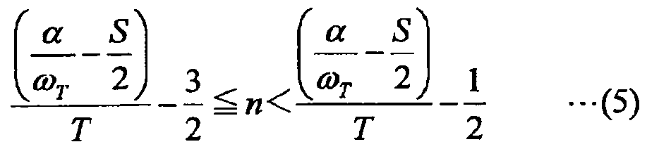
Claims
Priority Applications (6)
| Application Number | Priority Date | Filing Date | Title |
|---|---|---|---|
| KR1020137018019A KR101381341B1 (ko) | 2006-10-06 | 2007-10-05 | 가공 종점 검지방법, 연마방법 및 연마장치 |
| KR1020097009205A KR101357290B1 (ko) | 2006-10-06 | 2007-10-05 | 가공 종점 검지방법, 연마방법 및 연마장치 |
| CN2007800372892A CN101523565B (zh) | 2006-10-06 | 2007-10-05 | 加工终点检测方法、研磨方法及研磨装置 |
| JP2008538779A JP5006883B2 (ja) | 2006-10-06 | 2007-10-05 | 加工終点検知方法および加工装置 |
| US12/311,560 US8554356B2 (en) | 2006-10-06 | 2007-10-05 | Processing end point detection method, polishing method, and polishing apparatus |
| US14/017,620 US10207390B2 (en) | 2006-10-06 | 2013-09-04 | Processing end point detection method, polishing method, and polishing apparatus |
Applications Claiming Priority (4)
| Application Number | Priority Date | Filing Date | Title |
|---|---|---|---|
| JP2006274622 | 2006-10-06 | ||
| JP2006-274622 | 2006-10-06 | ||
| JP2006-330383 | 2006-12-07 | ||
| JP2006330383 | 2006-12-07 |
Related Child Applications (2)
| Application Number | Title | Priority Date | Filing Date |
|---|---|---|---|
| US12/311,560 A-371-Of-International US8554356B2 (en) | 2006-10-06 | 2007-10-05 | Processing end point detection method, polishing method, and polishing apparatus |
| US14/017,620 Division US10207390B2 (en) | 2006-10-06 | 2013-09-04 | Processing end point detection method, polishing method, and polishing apparatus |
Publications (1)
| Publication Number | Publication Date |
|---|---|
| WO2008044786A1 true WO2008044786A1 (fr) | 2008-04-17 |
Family
ID=39282970
Family Applications (1)
| Application Number | Title | Priority Date | Filing Date |
|---|---|---|---|
| PCT/JP2007/070030 Ceased WO2008044786A1 (fr) | 2006-10-06 | 2007-10-05 | Procédé de detection de point de fin d'usinage, procédé de rectification, et rectifieuse |
Country Status (6)
| Country | Link |
|---|---|
| US (2) | US8554356B2 (ja) |
| JP (2) | JP5006883B2 (ja) |
| KR (2) | KR101357290B1 (ja) |
| CN (2) | CN101523565B (ja) |
| TW (1) | TWI422798B (ja) |
| WO (1) | WO2008044786A1 (ja) |
Cited By (17)
| Publication number | Priority date | Publication date | Assignee | Title |
|---|---|---|---|---|
| JP2009291857A (ja) * | 2008-06-03 | 2009-12-17 | Ebara Corp | 研磨終点検知方法 |
| JP2010023210A (ja) * | 2008-07-23 | 2010-02-04 | Ebara Corp | 研磨終点検知方法および研磨装置 |
| JP2010036299A (ja) * | 2008-08-05 | 2010-02-18 | Ebara Corp | 研磨方法および装置 |
| JP2010115726A (ja) * | 2008-11-11 | 2010-05-27 | Ebara Corp | 研磨終点検知用の光の波長選択に用いられるダイヤグラムの作成方法、光の波長選択方法、研磨終点検出方法、研磨終点検出装置、および研磨装置 |
| JP2010120092A (ja) * | 2008-11-17 | 2010-06-03 | Nikon Corp | 終点検出装置および研磨装置 |
| JP2010253627A (ja) * | 2009-04-27 | 2010-11-11 | Ebara Corp | 研磨方法及び研磨装置及び基板の監視方法 |
| JP2011009679A (ja) * | 2009-05-27 | 2011-01-13 | Ebara Corp | 研磨終点検知方法、研磨終点検知装置、研磨方法、および研磨装置 |
| JP2011082286A (ja) * | 2009-10-06 | 2011-04-21 | Ebara Corp | 研磨終点検知方法および研磨終点検知装置 |
| JP2011520264A (ja) * | 2008-05-02 | 2011-07-14 | アプライド マテリアルズ インコーポレイテッド | 複数のスペクトルを使用する化学機械研磨での終点検出 |
| US8454407B2 (en) | 2008-08-05 | 2013-06-04 | Ebara Corporation | Polishing method and apparatus |
| JP2013110390A (ja) * | 2011-10-26 | 2013-06-06 | Ebara Corp | 研磨方法および研磨装置 |
| US8657644B2 (en) | 2009-07-16 | 2014-02-25 | Ebara Corporation | Eddy current sensor and polishing method and apparatus |
| JP2015156503A (ja) * | 2010-03-02 | 2015-08-27 | 株式会社荏原製作所 | 研磨監視方法、研磨監視装置、および研磨装置 |
| JP2016165792A (ja) * | 2015-03-05 | 2016-09-15 | ミクロ技研株式会社 | 研磨ヘッド及び研磨処理装置 |
| JP2017064894A (ja) * | 2015-10-02 | 2017-04-06 | ミクロ技研株式会社 | 研磨ヘッド及び研磨処理装置 |
| WO2017056636A1 (ja) * | 2015-09-28 | 2017-04-06 | 株式会社 荏原製作所 | 研磨方法および研磨装置 |
| JP2019075520A (ja) * | 2017-10-19 | 2019-05-16 | 株式会社荏原製作所 | 研磨装置、及び研磨方法 |
Families Citing this family (73)
| Publication number | Priority date | Publication date | Assignee | Title |
|---|---|---|---|---|
| US7306507B2 (en) | 2005-08-22 | 2007-12-11 | Applied Materials, Inc. | Polishing pad assembly with glass or crystalline window |
| US7998358B2 (en) | 2006-10-31 | 2011-08-16 | Applied Materials, Inc. | Peak-based endpointing for chemical mechanical polishing |
| US8751033B2 (en) * | 2008-11-14 | 2014-06-10 | Applied Materials, Inc. | Adaptive tracking spectrum features for endpoint detection |
| US8352061B2 (en) | 2008-11-14 | 2013-01-08 | Applied Materials, Inc. | Semi-quantitative thickness determination |
| US8157614B2 (en) * | 2009-04-30 | 2012-04-17 | Applied Materials, Inc. | Method of making and apparatus having windowless polishing pad and protected fiber |
| JP5968783B2 (ja) | 2009-11-03 | 2016-08-10 | アプライド マテリアルズ インコーポレイテッドApplied Materials,Incorporated | スペクトルの等高線図のピーク位置と時間の関係を使用する終点方法 |
| CN102136441B (zh) * | 2010-01-26 | 2012-09-26 | 中芯国际集成电路制造(上海)有限公司 | 化学机械研磨终点的检测方法 |
| CN102049733B (zh) * | 2010-07-26 | 2013-04-17 | 清华大学 | 电涡流金属膜厚度终点检测装置 |
| JP5980476B2 (ja) * | 2010-12-27 | 2016-08-31 | 株式会社荏原製作所 | ポリッシング装置およびポリッシング方法 |
| CN103313822B (zh) * | 2011-01-21 | 2016-04-20 | 株式会社捷太格特 | 磨削异常监视方法以及磨削异常监视装置 |
| US8547538B2 (en) * | 2011-04-21 | 2013-10-01 | Applied Materials, Inc. | Construction of reference spectra with variations in environmental effects |
| US8657646B2 (en) * | 2011-05-09 | 2014-02-25 | Applied Materials, Inc. | Endpoint detection using spectrum feature trajectories |
| US10215660B1 (en) * | 2011-11-10 | 2019-02-26 | Lockheed Martin Corporation | Erosion sensor and system, method, and computer program product thereof |
| CN102441839B (zh) * | 2011-11-11 | 2014-06-04 | 上海华力微电子有限公司 | 提高固定研磨料在研磨垫上进行cmp工艺稳定性的方法 |
| JP2013222856A (ja) * | 2012-04-17 | 2013-10-28 | Ebara Corp | 研磨装置および研磨方法 |
| CN103084968A (zh) * | 2013-02-27 | 2013-05-08 | 上海华力微电子有限公司 | 研磨终点探测方法、装置及研磨机台 |
| JP2014210276A (ja) * | 2013-04-17 | 2014-11-13 | 三菱マテリアル株式会社 | 回転体のレーザ加工方法及び加工装置 |
| JP6105371B2 (ja) | 2013-04-25 | 2017-03-29 | 株式会社荏原製作所 | 研磨方法および研磨装置 |
| JP6215602B2 (ja) * | 2013-07-11 | 2017-10-18 | 株式会社荏原製作所 | 研磨装置および研磨状態監視方法 |
| TWI635929B (zh) * | 2013-07-11 | 2018-09-21 | 日商荏原製作所股份有限公司 | 研磨裝置及研磨狀態監視方法 |
| US9227294B2 (en) * | 2013-12-31 | 2016-01-05 | Taiwan Semiconductor Manufacturing Company Ltd. | Apparatus and method for chemical mechanical polishing |
| JP6293519B2 (ja) * | 2014-03-05 | 2018-03-14 | 株式会社荏原製作所 | 研磨装置および研磨方法 |
| JP6266493B2 (ja) * | 2014-03-20 | 2018-01-24 | 株式会社荏原製作所 | 研磨装置及び研磨方法 |
| JP2015188955A (ja) * | 2014-03-27 | 2015-11-02 | 株式会社荏原製作所 | 研磨装置 |
| DE102015011013B4 (de) | 2014-08-22 | 2023-05-04 | Sigma Additive Solutions, Inc. | Verfahren zur Überwachung von generativen Fertigungsprozessen |
| KR102388170B1 (ko) * | 2014-09-02 | 2022-04-19 | 가부시키가이샤 에바라 세이사꾸쇼 | 종점 검출 방법, 연마 장치 및 연마 방법 |
| JP6532884B2 (ja) * | 2014-10-31 | 2019-06-19 | 株式会社荏原製作所 | ワークピースを研磨するための化学機械研磨装置 |
| US10786948B2 (en) | 2014-11-18 | 2020-09-29 | Sigma Labs, Inc. | Multi-sensor quality inference and control for additive manufacturing processes |
| CN104656529B (zh) * | 2015-01-04 | 2017-08-29 | 合肥鑫晟光电科技有限公司 | 用于基板加工的监控方法和监控装置 |
| EP3245045A4 (en) | 2015-01-13 | 2018-10-31 | Sigma Labs, Inc. | Material qualification system and methodology |
| CN105136046B (zh) * | 2015-05-15 | 2018-11-16 | 华南师范大学 | 激光干涉法薄膜厚度变化量在线监测方法和装置 |
| US9970754B2 (en) | 2015-08-26 | 2018-05-15 | Industrial Technology Research Institute | Surface measurement device and method thereof |
| US9835449B2 (en) | 2015-08-26 | 2017-12-05 | Industrial Technology Research Institute | Surface measuring device and method thereof |
| JP2017072583A (ja) * | 2015-08-26 | 2017-04-13 | 財團法人工業技術研究院Industrial Technology Research Institute | 表面測定装置及びその方法 |
| US10207489B2 (en) | 2015-09-30 | 2019-02-19 | Sigma Labs, Inc. | Systems and methods for additive manufacturing operations |
| JP6775354B2 (ja) * | 2015-10-16 | 2020-10-28 | 株式会社荏原製作所 | 研磨装置、及び、研磨方法 |
| US10744617B2 (en) | 2015-10-16 | 2020-08-18 | Ebara Corporation | Polishing endpoint detection method |
| CN207058321U (zh) * | 2016-05-11 | 2018-03-02 | 凯斯科技股份有限公司 | 具有氧化物层的晶片的抛光系统 |
| JP6469785B2 (ja) * | 2016-07-27 | 2019-02-13 | 株式会社荏原製作所 | 研磨パッド |
| TWI743176B (zh) | 2016-08-26 | 2021-10-21 | 美商應用材料股份有限公司 | 獲得代表在基板上的層的厚度的測量的方法,及量測系統和電腦程式產品 |
| CN106272072B (zh) * | 2016-08-29 | 2019-05-31 | 佛山市新鹏机器人技术有限公司 | 盥洗用具的抛光位置点测定方法和装置 |
| US10260865B1 (en) * | 2016-09-13 | 2019-04-16 | National Technology & Engineering Solutions Of Sandia, Llc | High resolution, non-contact removal rate module for serial sectioning |
| JP6800521B2 (ja) * | 2016-09-13 | 2020-12-16 | 株式会社ディスコ | 切削装置 |
| JP7062644B2 (ja) * | 2016-09-21 | 2022-05-06 | アプライド マテリアルズ インコーポレイテッド | フィルタリングのための補償を用いた終点検出 |
| JP2018083267A (ja) * | 2016-11-25 | 2018-05-31 | 株式会社荏原製作所 | 研磨装置及び研磨方法 |
| JP7023455B2 (ja) * | 2017-01-23 | 2022-02-22 | 不二越機械工業株式会社 | ワーク研磨方法およびワーク研磨装置 |
| JP7023062B2 (ja) | 2017-07-24 | 2022-02-21 | 株式会社荏原製作所 | 基板研磨装置及び方法 |
| JP6948868B2 (ja) * | 2017-07-24 | 2021-10-13 | 株式会社荏原製作所 | 研磨装置および研磨方法 |
| JP6860451B2 (ja) * | 2017-09-05 | 2021-04-14 | 株式会社荏原製作所 | 機能性チップを備える基板を研磨する方法 |
| CN107520740A (zh) * | 2017-09-18 | 2017-12-29 | 北京半导体专用设备研究所(中国电子科技集团公司第四十五研究所) | 一种化学机械抛光中光谱终点的检测方法、装置及系统 |
| JP6902452B2 (ja) * | 2017-10-19 | 2021-07-14 | 株式会社荏原製作所 | 研磨装置 |
| CN107617970A (zh) * | 2017-10-26 | 2018-01-23 | 北京半导体专用设备研究所(中国电子科技集团公司第四十五研究所) | 一种晶圆抛光终点的检测系统 |
| JP7074489B2 (ja) | 2018-02-08 | 2022-05-24 | 株式会社Screenホールディングス | データ処理方法、データ処理装置、および、データ処理プログラム |
| CN108535210B (zh) * | 2018-06-19 | 2023-12-05 | 北京市农林科学院信息技术研究中心 | 一种用于太赫兹光谱测量的样品研磨装置 |
| US11571782B2 (en) | 2018-11-28 | 2023-02-07 | Taiwan Semiconductor Manufacturing Co., Ltd. | Single bodied platen housing a detection module for CMP systems |
| TW202044394A (zh) * | 2019-05-22 | 2020-12-01 | 日商荏原製作所股份有限公司 | 基板處理系統 |
| JP7253458B2 (ja) * | 2019-06-27 | 2023-04-06 | 株式会社荏原製作所 | 光学式膜厚測定装置の最適な動作レシピを決定する方法、装置、およびシステム |
| CN110549240B (zh) * | 2019-09-18 | 2020-12-29 | 清华大学 | 一种终点检测方法和化学机械抛光装置 |
| JP7376317B2 (ja) | 2019-10-30 | 2023-11-08 | 株式会社Screenホールディングス | 基板処理方法 |
| JP7503418B2 (ja) * | 2020-05-14 | 2024-06-20 | 株式会社荏原製作所 | 膜厚測定装置、研磨装置及び膜厚測定方法 |
| TWI810069B (zh) * | 2020-06-08 | 2023-07-21 | 美商應用材料股份有限公司 | 用於在拋光相鄰導電層的堆疊期間的輪廓控制的系統、方法及電腦程式產品 |
| JP7508327B2 (ja) * | 2020-10-06 | 2024-07-01 | 株式会社荏原製作所 | 光学式膜厚測定装置および研磨装置 |
| KR20240161701A (ko) * | 2021-03-03 | 2024-11-12 | 어플라이드 머티어리얼스, 인코포레이티드 | 공간 분해능을 제공하기 위한 모터 토크 모니터링 동안의 압력 신호들 |
| US12322659B2 (en) | 2021-03-04 | 2025-06-03 | Applied Materials, Inc. | Pixel classification of film non-uniformity based on processing of substrate images |
| CN115446669B (zh) * | 2021-06-09 | 2025-08-19 | 北京晶亦精微科技股份有限公司 | 一种传感器与晶圆相对轨迹追踪方法 |
| US11901203B2 (en) | 2021-06-10 | 2024-02-13 | Applied Materials, Inc. | Substrate process endpoint detection using machine learning |
| US11965798B2 (en) * | 2021-06-10 | 2024-04-23 | Applied Materials, Inc. | Endpoint detection system for enhanced spectral data collection |
| CN113399784B (zh) * | 2021-07-09 | 2022-08-12 | 武汉武重机床有限公司 | 工件加工控制方法、装置、设备及存储介质 |
| CN114029790B (zh) * | 2021-11-25 | 2023-04-07 | 北京晶亦精微科技股份有限公司 | 一种晶圆研磨方法 |
| KR20250045736A (ko) | 2023-09-26 | 2025-04-02 | 김효성 | 자율주행 자동연마장치 |
| CN117067042B (zh) * | 2023-10-17 | 2024-01-30 | 杭州泓芯微半导体有限公司 | 一种研磨机及其控制方法 |
| CN118752405B (zh) * | 2024-09-02 | 2025-01-24 | 江苏元夫半导体科技有限公司 | 化学机械抛光的处理方法及装置、设备、存储介质 |
| CN119897756B (zh) * | 2025-04-02 | 2025-07-11 | 天通控股股份有限公司 | 一种提高钽酸锂键合片膜厚均匀性的方法 |
Citations (4)
| Publication number | Priority date | Publication date | Assignee | Title |
|---|---|---|---|---|
| JPH1133901A (ja) * | 1997-07-18 | 1999-02-09 | Nikon Corp | ウェハ研磨装置 |
| JP2000033561A (ja) * | 1998-07-21 | 2000-02-02 | Dainippon Screen Mfg Co Ltd | 終点検出装置、終点検出方法 |
| JP2004514273A (ja) * | 2000-07-31 | 2004-05-13 | エイエスエムエル ユーエス インコーポレイテッド | 化学機械研磨における終点検出のための原位置方法及び装置 |
| JP2004154928A (ja) * | 2002-10-17 | 2004-06-03 | Ebara Corp | 研磨状態監視装置、ポリッシング装置、及び研磨方法 |
Family Cites Families (92)
| Publication number | Priority date | Publication date | Assignee | Title |
|---|---|---|---|---|
| US5658183A (en) * | 1993-08-25 | 1997-08-19 | Micron Technology, Inc. | System for real-time control of semiconductor wafer polishing including optical monitoring |
| US5700180A (en) * | 1993-08-25 | 1997-12-23 | Micron Technology, Inc. | System for real-time control of semiconductor wafer polishing |
| US5891352A (en) * | 1993-09-16 | 1999-04-06 | Luxtron Corporation | Optical techniques of measuring endpoint during the processing of material layers in an optically hostile environment |
| US5644503A (en) * | 1994-03-28 | 1997-07-01 | Hitachi, Ltd. | Methods and apparatuses for analyzing multichannel chromatogram |
| EP0756318A1 (en) * | 1995-07-24 | 1997-01-29 | International Business Machines Corporation | Method for real-time in-situ monitoring of a trench formation process |
| JP3766991B2 (ja) * | 1995-10-20 | 2006-04-19 | 株式会社日立製作所 | プラズマ処理の終点検出方法及び装置、並びに本検出方法及び装置を用いた半導体製造方法及び装置 |
| US6146248A (en) * | 1997-05-28 | 2000-11-14 | Lam Research Corporation | Method and apparatus for in-situ end-point detection and optimization of a chemical-mechanical polishing process using a linear polisher |
| US6108091A (en) * | 1997-05-28 | 2000-08-22 | Lam Research Corporation | Method and apparatus for in-situ monitoring of thickness during chemical-mechanical polishing |
| US6489624B1 (en) * | 1997-07-18 | 2002-12-03 | Nikon Corporation | Apparatus and methods for detecting thickness of a patterned layer |
| US6950193B1 (en) * | 1997-10-28 | 2005-09-27 | Rockwell Automation Technologies, Inc. | System for monitoring substrate conditions |
| US6068539A (en) * | 1998-03-10 | 2000-05-30 | Lam Research Corporation | Wafer polishing device with movable window |
| US6248000B1 (en) * | 1998-03-24 | 2001-06-19 | Nikon Research Corporation Of America | Polishing pad thinning to optically access a semiconductor wafer surface |
| US6271047B1 (en) * | 1998-05-21 | 2001-08-07 | Nikon Corporation | Layer-thickness detection methods and apparatus for wafers and the like, and polishing apparatus comprising same |
| US6241847B1 (en) * | 1998-06-30 | 2001-06-05 | Lsi Logic Corporation | Method and apparatus for detecting a polishing endpoint based upon infrared signals |
| US6077783A (en) * | 1998-06-30 | 2000-06-20 | Lsi Logic Corporation | Method and apparatus for detecting a polishing endpoint based upon heat conducted through a semiconductor wafer |
| US6172756B1 (en) * | 1998-12-11 | 2001-01-09 | Filmetrics, Inc. | Rapid and accurate end point detection in a noisy environment |
| US6204922B1 (en) * | 1998-12-11 | 2001-03-20 | Filmetrics, Inc. | Rapid and accurate thin film measurement of individual layers in a multi-layered or patterned sample |
| US6117779A (en) * | 1998-12-15 | 2000-09-12 | Lsi Logic Corporation | Endpoint detection method and apparatus which utilize a chelating agent to detect a polishing endpoint |
| US6354922B1 (en) * | 1999-08-20 | 2002-03-12 | Ebara Corporation | Polishing apparatus |
| US6358128B1 (en) * | 1999-03-05 | 2002-03-19 | Ebara Corporation | Polishing apparatus |
| JP3327289B2 (ja) * | 2000-03-29 | 2002-09-24 | 株式会社ニコン | 工程終了点測定装置及び測定方法及び研磨装置及び半導体デバイス製造方法及び信号処理プログラムを記録した記録媒体 |
| WO2000071971A1 (en) * | 1999-05-24 | 2000-11-30 | Luxtron Corporation | Optical techniques for measuring layer thicknesses |
| US6570662B1 (en) * | 1999-05-24 | 2003-05-27 | Luxtron Corporation | Optical techniques for measuring layer thicknesses and other surface characteristics of objects such as semiconductor wafers |
| US6776692B1 (en) * | 1999-07-09 | 2004-08-17 | Applied Materials Inc. | Closed-loop control of wafer polishing in a chemical mechanical polishing system |
| US6273792B1 (en) * | 1999-08-11 | 2001-08-14 | Speedfam-Ipec Corporation | Method and apparatus for in-situ measurement of workpiece displacement during chemical mechanical polishing |
| US6306008B1 (en) * | 1999-08-31 | 2001-10-23 | Micron Technology, Inc. | Apparatus and method for conditioning and monitoring media used for chemical-mechanical planarization |
| US6630995B1 (en) * | 1999-09-07 | 2003-10-07 | Applied Materials, Inc. | Method and apparatus for embedded substrate and system status monitoring |
| US6671051B1 (en) * | 1999-09-15 | 2003-12-30 | Kla-Tencor | Apparatus and methods for detecting killer particles during chemical mechanical polishing |
| US6628397B1 (en) * | 1999-09-15 | 2003-09-30 | Kla-Tencor | Apparatus and methods for performing self-clearing optical measurements |
| US6520843B1 (en) * | 1999-10-27 | 2003-02-18 | Strasbaugh | High planarity chemical mechanical planarization |
| US6629874B1 (en) * | 1999-10-27 | 2003-10-07 | Strasbaugh | Feature height measurement during CMP |
| US6976901B1 (en) * | 1999-10-27 | 2005-12-20 | Strasbaugh | In situ feature height measurement |
| US6517419B1 (en) * | 1999-10-27 | 2003-02-11 | Strasbaugh | Shaping polishing pad for small head chemical mechanical planarization |
| US6514121B1 (en) * | 1999-10-27 | 2003-02-04 | Strasbaugh | Polishing chemical delivery for small head chemical mechanical planarization |
| JP3259225B2 (ja) * | 1999-12-27 | 2002-02-25 | 株式会社ニコン | 研磨状況モニタ方法及びその装置、研磨装置、プロセスウエハ、半導体デバイス製造方法、並びに半導体デバイス |
| US20020023715A1 (en) * | 2000-05-26 | 2002-02-28 | Norio Kimura | Substrate polishing apparatus and substrate polishing mehod |
| JP3832198B2 (ja) * | 2000-06-16 | 2006-10-11 | 日本電気株式会社 | 半導体ウェハの研磨終点検出方法ならびにその装置 |
| US6878038B2 (en) * | 2000-07-10 | 2005-04-12 | Applied Materials Inc. | Combined eddy current sensing and optical monitoring for chemical mechanical polishing |
| US6602724B2 (en) * | 2000-07-27 | 2003-08-05 | Applied Materials, Inc. | Chemical mechanical polishing of a metal layer with polishing rate monitoring |
| US6476921B1 (en) * | 2000-07-31 | 2002-11-05 | Asml Us, Inc. | In-situ method and apparatus for end point detection in chemical mechanical polishing |
| US7134934B2 (en) * | 2000-08-30 | 2006-11-14 | Micron Technology, Inc. | Methods and apparatus for electrically detecting characteristics of a microelectronic substrate and/or polishing medium |
| TW464588B (en) * | 2000-08-31 | 2001-11-21 | United Microelectronics Corp | Device for detecting abnormality of chemical mechanical polishing |
| US6809809B2 (en) * | 2000-11-15 | 2004-10-26 | Real Time Metrology, Inc. | Optical method and apparatus for inspecting large area planar objects |
| JP4810728B2 (ja) * | 2000-12-04 | 2011-11-09 | 株式会社ニコン | 研磨状況モニタ方法及びその装置、研磨装置、並びに半導体デバイス製造方法 |
| US6491569B2 (en) * | 2001-04-19 | 2002-12-10 | Speedfam-Ipec Corporation | Method and apparatus for using optical reflection data to obtain a continuous predictive signal during CMP |
| US6676482B2 (en) * | 2001-04-20 | 2004-01-13 | Speedfam-Ipec Corporation | Learning method and apparatus for predictive determination of endpoint during chemical mechanical planarization using sparse sampling |
| US6966816B2 (en) * | 2001-05-02 | 2005-11-22 | Applied Materials, Inc. | Integrated endpoint detection system with optical and eddy current monitoring |
| US6821794B2 (en) * | 2001-10-04 | 2004-11-23 | Novellus Systems, Inc. | Flexible snapshot in endpoint detection |
| US6635573B2 (en) * | 2001-10-29 | 2003-10-21 | Applied Materials, Inc | Method of detecting an endpoint during etching of a material within a recess |
| US7074110B1 (en) * | 2001-11-23 | 2006-07-11 | Stephan H Wolf | Optical coupler hub for chemical-mechanical-planarization polishing pads with an integrated optical waveguide |
| US7024268B1 (en) * | 2002-03-22 | 2006-04-04 | Applied Materials Inc. | Feedback controlled polishing processes |
| US6908846B2 (en) * | 2002-10-24 | 2005-06-21 | Lam Research Corporation | Method and apparatus for detecting endpoint during plasma etching of thin films |
| US6991514B1 (en) * | 2003-02-21 | 2006-01-31 | Verity Instruments, Inc. | Optical closed-loop control system for a CMP apparatus and method of manufacture thereof |
| US6945845B2 (en) * | 2003-03-04 | 2005-09-20 | Applied Materials, Inc. | Chemical mechanical polishing apparatus with non-conductive elements |
| US6972848B2 (en) * | 2003-03-04 | 2005-12-06 | Hitach High-Technologies Corporation | Semiconductor fabricating apparatus with function of determining etching processing state |
| JP2006522493A (ja) * | 2003-04-01 | 2006-09-28 | フィルメトリックス・インコーポレイテッド | Cmpのための基板全体用スペクトル画像形成システム |
| US20050023149A1 (en) * | 2003-06-05 | 2005-02-03 | Tsutomu Nakada | Plating apparatus, plating method and substrate processing apparatus |
| US7008296B2 (en) * | 2003-06-18 | 2006-03-07 | Applied Materials, Inc. | Data processing for monitoring chemical mechanical polishing |
| JP2005029830A (ja) * | 2003-07-10 | 2005-02-03 | Ebara Corp | めっき装置及びめっき方法 |
| JP2005051093A (ja) | 2003-07-30 | 2005-02-24 | Shimadzu Corp | データ収集装置、及び該装置を用いた基板研磨装置 |
| US7025658B2 (en) * | 2003-08-18 | 2006-04-11 | Applied Materials, Inc. | Platen and head rotation rates for monitoring chemical mechanical polishing |
| US7153185B1 (en) * | 2003-08-18 | 2006-12-26 | Applied Materials, Inc. | Substrate edge detection |
| US6991516B1 (en) * | 2003-08-18 | 2006-01-31 | Applied Materials Inc. | Chemical mechanical polishing with multi-stage monitoring of metal clearing |
| US7097537B1 (en) * | 2003-08-18 | 2006-08-29 | Applied Materials, Inc. | Determination of position of sensor measurements during polishing |
| US20050051437A1 (en) * | 2003-09-04 | 2005-03-10 | Keiichi Kurashina | Plating apparatus and plating method |
| JP4464642B2 (ja) | 2003-09-10 | 2010-05-19 | 株式会社荏原製作所 | 研磨状態監視装置、研磨状態監視方法、研磨装置及び研磨方法 |
| US20050066739A1 (en) * | 2003-09-26 | 2005-03-31 | Lam Research Corporation | Method and apparatus for wafer mechanical stress monitoring and wafer thermal stress monitoring |
| US20050173259A1 (en) * | 2004-02-06 | 2005-08-11 | Applied Materials, Inc. | Endpoint system for electro-chemical mechanical polishing |
| US8110814B2 (en) * | 2003-10-16 | 2012-02-07 | Alis Corporation | Ion sources, systems and methods |
| US20060166608A1 (en) * | 2004-04-01 | 2006-07-27 | Chalmers Scott A | Spectral imaging of substrates |
| EP1758711B1 (en) | 2004-06-21 | 2013-08-07 | Ebara Corporation | Polishing apparatus and polishing method |
| JP4641395B2 (ja) * | 2004-08-17 | 2011-03-02 | Okiセミコンダクタ株式会社 | 半導体装置の研削方法、及び研削装置 |
| US20070205112A1 (en) * | 2004-08-27 | 2007-09-06 | Masako Kodera | Polishing apparatus and polishing method |
| WO2006022452A2 (en) * | 2004-08-27 | 2006-03-02 | Ebara Corporation | Polishing apparatus and polishing method |
| US7565084B1 (en) * | 2004-09-15 | 2009-07-21 | Wach Michael L | Robustly stabilizing laser systems |
| DE102004058133B4 (de) * | 2004-12-02 | 2006-11-09 | Infineon Technologies Ag | Verfahren zum Überwachen eines CMP-Polierverfahrens und Anordnung zur Durchführung eines CMP-Polierverfahrens |
| US7728967B2 (en) * | 2005-07-07 | 2010-06-01 | Kabushiki Kaisha Toshiba | Laser-based maintenance apparatus |
| KR100716935B1 (ko) * | 2005-11-25 | 2007-05-14 | 두산디앤디 주식회사 | 반도체 웨이퍼의 화학기계적 연마장치용 로딩디바이스 |
| EP1983558A4 (en) * | 2006-02-06 | 2011-08-10 | Toray Industries | ABRASION PAD AND ABRASION DEVICE |
| JP2007287939A (ja) * | 2006-04-17 | 2007-11-01 | Ebara Corp | 研磨方法、及び研磨装置 |
| US7494929B2 (en) * | 2006-04-27 | 2009-02-24 | Applied Materials, Inc. | Automatic gain control |
| JP5283506B2 (ja) * | 2006-09-12 | 2013-09-04 | 株式会社荏原製作所 | 研磨装置および研磨方法 |
| US7998358B2 (en) * | 2006-10-31 | 2011-08-16 | Applied Materials, Inc. | Peak-based endpointing for chemical mechanical polishing |
| US20080188162A1 (en) * | 2007-02-06 | 2008-08-07 | Itsuki Kobata | Electrochemical mechanical polishing apparatus conditioning method, and conditioning solution |
| JP5219395B2 (ja) * | 2007-03-29 | 2013-06-26 | 株式会社東京精密 | ウェハ研磨モニタ方法とその装置 |
| US7840375B2 (en) * | 2007-04-02 | 2010-11-23 | Applied Materials, Inc. | Methods and apparatus for generating a library of spectra |
| JP2009026850A (ja) * | 2007-07-18 | 2009-02-05 | Elpida Memory Inc | Cmp装置及びcmpによるウェハー研磨方法 |
| JP2009033038A (ja) * | 2007-07-30 | 2009-02-12 | Elpida Memory Inc | Cmp装置及びcmpによるウェハー研磨方法 |
| US8870625B2 (en) * | 2007-11-28 | 2014-10-28 | Ebara Corporation | Method and apparatus for dressing polishing pad, profile measuring method, substrate polishing apparatus, and substrate polishing method |
| JP5248127B2 (ja) * | 2008-01-30 | 2013-07-31 | 株式会社荏原製作所 | 研磨方法及び研磨装置 |
| JP5254668B2 (ja) * | 2008-06-03 | 2013-08-07 | 株式会社荏原製作所 | 研磨終点検出方法 |
| US8388408B2 (en) * | 2008-10-10 | 2013-03-05 | Ebara Corporation | Method of making diagram for use in selection of wavelength of light for polishing endpoint detection, method for selecting wavelength of light for polishing endpoint detection, and polishing endpoint detection method |
-
2007
- 2007-10-05 TW TW096137408A patent/TWI422798B/zh active
- 2007-10-05 JP JP2008538779A patent/JP5006883B2/ja active Active
- 2007-10-05 KR KR1020097009205A patent/KR101357290B1/ko active Active
- 2007-10-05 CN CN2007800372892A patent/CN101523565B/zh active Active
- 2007-10-05 KR KR1020137018019A patent/KR101381341B1/ko active Active
- 2007-10-05 WO PCT/JP2007/070030 patent/WO2008044786A1/ja not_active Ceased
- 2007-10-05 US US12/311,560 patent/US8554356B2/en active Active
- 2007-10-05 CN CN201110416880.7A patent/CN102490112B/zh active Active
-
2010
- 2010-06-22 JP JP2010141522A patent/JP2010240837A/ja active Pending
-
2013
- 2013-09-04 US US14/017,620 patent/US10207390B2/en active Active
Patent Citations (4)
| Publication number | Priority date | Publication date | Assignee | Title |
|---|---|---|---|---|
| JPH1133901A (ja) * | 1997-07-18 | 1999-02-09 | Nikon Corp | ウェハ研磨装置 |
| JP2000033561A (ja) * | 1998-07-21 | 2000-02-02 | Dainippon Screen Mfg Co Ltd | 終点検出装置、終点検出方法 |
| JP2004514273A (ja) * | 2000-07-31 | 2004-05-13 | エイエスエムエル ユーエス インコーポレイテッド | 化学機械研磨における終点検出のための原位置方法及び装置 |
| JP2004154928A (ja) * | 2002-10-17 | 2004-06-03 | Ebara Corp | 研磨状態監視装置、ポリッシング装置、及び研磨方法 |
Cited By (23)
| Publication number | Priority date | Publication date | Assignee | Title |
|---|---|---|---|---|
| JP2011520264A (ja) * | 2008-05-02 | 2011-07-14 | アプライド マテリアルズ インコーポレイテッド | 複数のスペクトルを使用する化学機械研磨での終点検出 |
| JP2009291857A (ja) * | 2008-06-03 | 2009-12-17 | Ebara Corp | 研磨終点検知方法 |
| US8157616B2 (en) | 2008-06-03 | 2012-04-17 | Ebara Corporation | Polishing end point detection method |
| JP2010023210A (ja) * | 2008-07-23 | 2010-02-04 | Ebara Corp | 研磨終点検知方法および研磨装置 |
| JP2010036299A (ja) * | 2008-08-05 | 2010-02-18 | Ebara Corp | 研磨方法および装置 |
| US8454407B2 (en) | 2008-08-05 | 2013-06-04 | Ebara Corporation | Polishing method and apparatus |
| JP2010115726A (ja) * | 2008-11-11 | 2010-05-27 | Ebara Corp | 研磨終点検知用の光の波長選択に用いられるダイヤグラムの作成方法、光の波長選択方法、研磨終点検出方法、研磨終点検出装置、および研磨装置 |
| JP2010120092A (ja) * | 2008-11-17 | 2010-06-03 | Nikon Corp | 終点検出装置および研磨装置 |
| JP2010253627A (ja) * | 2009-04-27 | 2010-11-11 | Ebara Corp | 研磨方法及び研磨装置及び基板の監視方法 |
| JP2011009679A (ja) * | 2009-05-27 | 2011-01-13 | Ebara Corp | 研磨終点検知方法、研磨終点検知装置、研磨方法、および研磨装置 |
| US8657644B2 (en) | 2009-07-16 | 2014-02-25 | Ebara Corporation | Eddy current sensor and polishing method and apparatus |
| JP2011082286A (ja) * | 2009-10-06 | 2011-04-21 | Ebara Corp | 研磨終点検知方法および研磨終点検知装置 |
| US8777694B2 (en) | 2009-10-06 | 2014-07-15 | Ebara Corporation | Polishing endpoint detection method |
| JP2015156503A (ja) * | 2010-03-02 | 2015-08-27 | 株式会社荏原製作所 | 研磨監視方法、研磨監視装置、および研磨装置 |
| JP2013110390A (ja) * | 2011-10-26 | 2013-06-06 | Ebara Corp | 研磨方法および研磨装置 |
| JP2016165792A (ja) * | 2015-03-05 | 2016-09-15 | ミクロ技研株式会社 | 研磨ヘッド及び研磨処理装置 |
| WO2017056636A1 (ja) * | 2015-09-28 | 2017-04-06 | 株式会社 荏原製作所 | 研磨方法および研磨装置 |
| JP2017064801A (ja) * | 2015-09-28 | 2017-04-06 | 株式会社荏原製作所 | 研磨方法および研磨装置 |
| US10569381B2 (en) | 2015-09-28 | 2020-02-25 | Ebara Corporation | Polishing method and polishing apparatus |
| TWI719036B (zh) * | 2015-09-28 | 2021-02-21 | 日商荏原製作所股份有限公司 | 研磨方法及研磨裝置 |
| JP2017064894A (ja) * | 2015-10-02 | 2017-04-06 | ミクロ技研株式会社 | 研磨ヘッド及び研磨処理装置 |
| JP2019075520A (ja) * | 2017-10-19 | 2019-05-16 | 株式会社荏原製作所 | 研磨装置、及び研磨方法 |
| JP7141204B2 (ja) | 2017-10-19 | 2022-09-22 | 株式会社荏原製作所 | 研磨装置、及び研磨方法 |
Also Published As
| Publication number | Publication date |
|---|---|
| US20140004773A1 (en) | 2014-01-02 |
| US8554356B2 (en) | 2013-10-08 |
| CN101523565A (zh) | 2009-09-02 |
| CN102490112B (zh) | 2015-03-25 |
| KR101381341B1 (ko) | 2014-04-04 |
| CN102490112A (zh) | 2012-06-13 |
| KR20090083360A (ko) | 2009-08-03 |
| TWI422798B (zh) | 2014-01-11 |
| KR101357290B1 (ko) | 2014-01-28 |
| KR20130088895A (ko) | 2013-08-08 |
| JP5006883B2 (ja) | 2012-08-22 |
| JP2010240837A (ja) | 2010-10-28 |
| US20100015889A1 (en) | 2010-01-21 |
| CN101523565B (zh) | 2012-02-29 |
| US10207390B2 (en) | 2019-02-19 |
| TW200827659A (en) | 2008-07-01 |
| JPWO2008044786A1 (ja) | 2010-02-18 |
Similar Documents
| Publication | Publication Date | Title |
|---|---|---|
| WO2008044786A1 (fr) | Procédé de detection de point de fin d'usinage, procédé de rectification, et rectifieuse | |
| JP5137910B2 (ja) | ポリッシング装置及び研磨方法 | |
| US8585460B2 (en) | Method of making diagram for use in selection of wavelength of light for polishing endpoint detection, method and apparatus for selecting wavelength of light for polishing endpoint detection, polishing endpoint detection method, polishing endpoint detection apparatus, and polishing monitoring method | |
| TW491753B (en) | In-situ method and apparatus for end point detection in chemical mechanical polishing | |
| CN109382755B (zh) | 基板研磨装置及方法 | |
| JP4542324B2 (ja) | 研磨状態監視装置及びポリッシング装置 | |
| TWI521625B (zh) | 使用光譜監測來偵測層級清除 | |
| KR102036387B1 (ko) | 연마 방법 및 연마 장치 | |
| KR101918803B1 (ko) | 푸리에 변환을 이용한 막 두께의 측정 | |
| US9372116B2 (en) | Automatic initiation of reference spectra library generation for optical monitoring | |
| TW201223702A (en) | Techniques for matching measured spectra to reference spectra for in-situ optical monitoring | |
| US20110269377A1 (en) | Automatic Generation of Reference Spectra for Optical Monitoring of Substrates | |
| CN102017094A (zh) | 在使用多个光谱的化学机械抛光中的终点检测 | |
| TWI569318B (zh) | Grinding apparatus and grinding method | |
| JP5436969B2 (ja) | 研磨終点検知方法、研磨終点検知装置、研磨方法、および研磨装置 | |
| TWI382484B (zh) | 決定光譜中銅濃度之方法 | |
| TWI726847B (zh) | 製造基板的方法,及其電腦程式產品和積體電路製造系統 |
Legal Events
| Date | Code | Title | Description |
|---|---|---|---|
| WWE | Wipo information: entry into national phase |
Ref document number: 200780037289.2 Country of ref document: CN |
|
| 121 | Ep: the epo has been informed by wipo that ep was designated in this application |
Ref document number: 07829765 Country of ref document: EP Kind code of ref document: A1 |
|
| WWE | Wipo information: entry into national phase |
Ref document number: 2008538779 Country of ref document: JP |
|
| WWE | Wipo information: entry into national phase |
Ref document number: 12311560 Country of ref document: US |
|
| NENP | Non-entry into the national phase |
Ref country code: DE |
|
| WWE | Wipo information: entry into national phase |
Ref document number: 1020097009205 Country of ref document: KR |
|
| 122 | Ep: pct application non-entry in european phase |
Ref document number: 07829765 Country of ref document: EP Kind code of ref document: A1 |
|
| WWE | Wipo information: entry into national phase |
Ref document number: 1020137018019 Country of ref document: KR |