KR20170044209A - Semiconductor device - Google Patents
Semiconductor device Download PDFInfo
- Publication number
- KR20170044209A KR20170044209A KR1020177009832A KR20177009832A KR20170044209A KR 20170044209 A KR20170044209 A KR 20170044209A KR 1020177009832 A KR1020177009832 A KR 1020177009832A KR 20177009832 A KR20177009832 A KR 20177009832A KR 20170044209 A KR20170044209 A KR 20170044209A
- Authority
- KR
- South Korea
- Prior art keywords
- transistor
- electrode
- insulating layer
- oxide semiconductor
- potential
- Prior art date
Links
- 239000004065 semiconductor Substances 0.000 title claims abstract description 470
- 239000000758 substrate Substances 0.000 claims abstract description 71
- 238000000034 method Methods 0.000 claims description 95
- 239000003990 capacitor Substances 0.000 claims description 33
- 229910052710 silicon Inorganic materials 0.000 claims description 24
- 239000010703 silicon Substances 0.000 claims description 24
- 239000004020 conductor Substances 0.000 claims description 15
- 239000013078 crystal Substances 0.000 claims description 8
- 229910052733 gallium Inorganic materials 0.000 claims description 6
- 229910052738 indium Inorganic materials 0.000 claims description 6
- 239000011701 zinc Substances 0.000 claims description 5
- 229910052725 zinc Inorganic materials 0.000 claims description 4
- GYHNNYVSQQEPJS-UHFFFAOYSA-N Gallium Chemical compound [Ga] GYHNNYVSQQEPJS-UHFFFAOYSA-N 0.000 claims description 3
- HCHKCACWOHOZIP-UHFFFAOYSA-N Zinc Chemical compound [Zn] HCHKCACWOHOZIP-UHFFFAOYSA-N 0.000 claims 2
- APFVFJFRJDLVQX-UHFFFAOYSA-N indium atom Chemical compound [In] APFVFJFRJDLVQX-UHFFFAOYSA-N 0.000 claims 2
- 230000015654 memory Effects 0.000 abstract description 133
- 239000000463 material Substances 0.000 abstract description 63
- 239000010410 layer Substances 0.000 description 483
- 239000011229 interlayer Substances 0.000 description 83
- 239000010408 film Substances 0.000 description 78
- 238000010438 heat treatment Methods 0.000 description 52
- 239000012535 impurity Substances 0.000 description 49
- 239000001257 hydrogen Substances 0.000 description 38
- 229910052739 hydrogen Inorganic materials 0.000 description 38
- 238000005530 etching Methods 0.000 description 36
- UFHFLCQGNIYNRP-UHFFFAOYSA-N Hydrogen Chemical compound [H][H] UFHFLCQGNIYNRP-UHFFFAOYSA-N 0.000 description 31
- 239000007789 gas Substances 0.000 description 31
- 238000010586 diagram Methods 0.000 description 29
- 238000004519 manufacturing process Methods 0.000 description 26
- 230000002829 reductive effect Effects 0.000 description 26
- 239000010936 titanium Substances 0.000 description 26
- 230000001681 protective effect Effects 0.000 description 25
- 229910052719 titanium Inorganic materials 0.000 description 25
- RTAQQCXQSZGOHL-UHFFFAOYSA-N Titanium Chemical compound [Ti] RTAQQCXQSZGOHL-UHFFFAOYSA-N 0.000 description 23
- XUIMIQQOPSSXEZ-UHFFFAOYSA-N Silicon Chemical compound [Si] XUIMIQQOPSSXEZ-UHFFFAOYSA-N 0.000 description 22
- XKRFYHLGVUSROY-UHFFFAOYSA-N Argon Chemical compound [Ar] XKRFYHLGVUSROY-UHFFFAOYSA-N 0.000 description 20
- 230000006870 function Effects 0.000 description 20
- 150000002736 metal compounds Chemical group 0.000 description 20
- 230000015572 biosynthetic process Effects 0.000 description 19
- 229910052760 oxygen Inorganic materials 0.000 description 19
- 238000004544 sputter deposition Methods 0.000 description 19
- 229910052581 Si3N4 Inorganic materials 0.000 description 18
- 239000012298 atmosphere Substances 0.000 description 18
- QVGXLLKOCUKJST-UHFFFAOYSA-N atomic oxygen Chemical compound [O] QVGXLLKOCUKJST-UHFFFAOYSA-N 0.000 description 18
- 239000001301 oxygen Substances 0.000 description 18
- HQVNEWCFYHHQES-UHFFFAOYSA-N silicon nitride Chemical compound N12[Si]34N5[Si]62N3[Si]51N64 HQVNEWCFYHHQES-UHFFFAOYSA-N 0.000 description 18
- 238000005229 chemical vapour deposition Methods 0.000 description 15
- 238000005240 physical vapour deposition Methods 0.000 description 15
- XLOMVQKBTHCTTD-UHFFFAOYSA-N Zinc monoxide Chemical compound [Zn]=O XLOMVQKBTHCTTD-UHFFFAOYSA-N 0.000 description 14
- 230000006866 deterioration Effects 0.000 description 14
- 238000005259 measurement Methods 0.000 description 14
- 229910052751 metal Inorganic materials 0.000 description 14
- 239000002184 metal Substances 0.000 description 14
- 230000008569 process Effects 0.000 description 14
- XLYOFNOQVPJJNP-UHFFFAOYSA-N water Substances O XLYOFNOQVPJJNP-UHFFFAOYSA-N 0.000 description 14
- 229910001868 water Inorganic materials 0.000 description 14
- 238000003860 storage Methods 0.000 description 13
- 229910010271 silicon carbide Inorganic materials 0.000 description 12
- WFKWXMTUELFFGS-UHFFFAOYSA-N tungsten Chemical compound [W] WFKWXMTUELFFGS-UHFFFAOYSA-N 0.000 description 12
- 229910052721 tungsten Inorganic materials 0.000 description 12
- 239000010937 tungsten Substances 0.000 description 12
- NRTOMJZYCJJWKI-UHFFFAOYSA-N Titanium nitride Chemical compound [Ti]#N NRTOMJZYCJJWKI-UHFFFAOYSA-N 0.000 description 11
- 229910007541 Zn O Inorganic materials 0.000 description 11
- 229910052782 aluminium Inorganic materials 0.000 description 11
- XAGFODPZIPBFFR-UHFFFAOYSA-N aluminium Chemical compound [Al] XAGFODPZIPBFFR-UHFFFAOYSA-N 0.000 description 11
- 229910052786 argon Inorganic materials 0.000 description 11
- IJGRMHOSHXDMSA-UHFFFAOYSA-N Atomic nitrogen Chemical compound N#N IJGRMHOSHXDMSA-UHFFFAOYSA-N 0.000 description 10
- 230000004888 barrier function Effects 0.000 description 10
- 238000001312 dry etching Methods 0.000 description 10
- VYPSYNLAJGMNEJ-UHFFFAOYSA-N silicon dioxide Inorganic materials O=[Si]=O VYPSYNLAJGMNEJ-UHFFFAOYSA-N 0.000 description 10
- 229910052814 silicon oxide Inorganic materials 0.000 description 9
- RYGMFSIKBFXOCR-UHFFFAOYSA-N Copper Chemical compound [Cu] RYGMFSIKBFXOCR-UHFFFAOYSA-N 0.000 description 8
- 229910052802 copper Inorganic materials 0.000 description 8
- 239000010949 copper Substances 0.000 description 8
- 238000002955 isolation Methods 0.000 description 8
- HBMJWWWQQXIZIP-UHFFFAOYSA-N silicon carbide Chemical compound [Si+]#[C-] HBMJWWWQQXIZIP-UHFFFAOYSA-N 0.000 description 8
- 150000001875 compounds Chemical class 0.000 description 7
- 229910000449 hafnium oxide Inorganic materials 0.000 description 7
- WIHZLLGSGQNAGK-UHFFFAOYSA-N hafnium(4+);oxygen(2-) Chemical compound [O-2].[O-2].[Hf+4] WIHZLLGSGQNAGK-UHFFFAOYSA-N 0.000 description 7
- 150000002431 hydrogen Chemical class 0.000 description 7
- 238000005268 plasma chemical vapour deposition Methods 0.000 description 7
- 238000012545 processing Methods 0.000 description 7
- 229910052715 tantalum Inorganic materials 0.000 description 7
- GUVRBAGPIYLISA-UHFFFAOYSA-N tantalum atom Chemical compound [Ta] GUVRBAGPIYLISA-UHFFFAOYSA-N 0.000 description 7
- 239000011787 zinc oxide Substances 0.000 description 7
- 238000004891 communication Methods 0.000 description 6
- 230000005684 electric field Effects 0.000 description 6
- 230000010354 integration Effects 0.000 description 6
- 229910052757 nitrogen Inorganic materials 0.000 description 6
- 239000011241 protective layer Substances 0.000 description 6
- 238000001039 wet etching Methods 0.000 description 6
- VYZAMTAEIAYCRO-UHFFFAOYSA-N Chromium Chemical compound [Cr] VYZAMTAEIAYCRO-UHFFFAOYSA-N 0.000 description 5
- ZOKXTWBITQBERF-UHFFFAOYSA-N Molybdenum Chemical compound [Mo] ZOKXTWBITQBERF-UHFFFAOYSA-N 0.000 description 5
- OAICVXFJPJFONN-UHFFFAOYSA-N Phosphorus Chemical compound [P] OAICVXFJPJFONN-UHFFFAOYSA-N 0.000 description 5
- 125000004429 atom Chemical group 0.000 description 5
- 230000008901 benefit Effects 0.000 description 5
- 230000008859 change Effects 0.000 description 5
- 229910052804 chromium Inorganic materials 0.000 description 5
- 239000011651 chromium Substances 0.000 description 5
- 230000007547 defect Effects 0.000 description 5
- 230000000694 effects Effects 0.000 description 5
- 229910052734 helium Inorganic materials 0.000 description 5
- 239000011261 inert gas Substances 0.000 description 5
- 230000014759 maintenance of location Effects 0.000 description 5
- 239000007769 metal material Substances 0.000 description 5
- 229910052750 molybdenum Inorganic materials 0.000 description 5
- 239000011733 molybdenum Substances 0.000 description 5
- TWNQGVIAIRXVLR-UHFFFAOYSA-N oxo(oxoalumanyloxy)alumane Chemical compound O=[Al]O[Al]=O TWNQGVIAIRXVLR-UHFFFAOYSA-N 0.000 description 5
- BPUBBGLMJRNUCC-UHFFFAOYSA-N oxygen(2-);tantalum(5+) Chemical compound [O-2].[O-2].[O-2].[O-2].[O-2].[Ta+5].[Ta+5] BPUBBGLMJRNUCC-UHFFFAOYSA-N 0.000 description 5
- 229910052698 phosphorus Inorganic materials 0.000 description 5
- 239000011574 phosphorus Substances 0.000 description 5
- 238000009832 plasma treatment Methods 0.000 description 5
- 238000005498 polishing Methods 0.000 description 5
- 239000002356 single layer Substances 0.000 description 5
- 229910001936 tantalum oxide Inorganic materials 0.000 description 5
- 208000005156 Dehydration Diseases 0.000 description 4
- 229910052779 Neodymium Inorganic materials 0.000 description 4
- 230000009471 action Effects 0.000 description 4
- 229910052785 arsenic Inorganic materials 0.000 description 4
- RQNWIZPPADIBDY-UHFFFAOYSA-N arsenic atom Chemical compound [As] RQNWIZPPADIBDY-UHFFFAOYSA-N 0.000 description 4
- 239000000460 chlorine Substances 0.000 description 4
- 230000018044 dehydration Effects 0.000 description 4
- 238000006297 dehydration reaction Methods 0.000 description 4
- 238000006356 dehydrogenation reaction Methods 0.000 description 4
- 238000011156 evaluation Methods 0.000 description 4
- 239000001307 helium Substances 0.000 description 4
- SWQJXJOGLNCZEY-UHFFFAOYSA-N helium atom Chemical compound [He] SWQJXJOGLNCZEY-UHFFFAOYSA-N 0.000 description 4
- 125000004435 hydrogen atom Chemical group [H]* 0.000 description 4
- 239000011810 insulating material Substances 0.000 description 4
- 239000011159 matrix material Substances 0.000 description 4
- 229910021421 monocrystalline silicon Inorganic materials 0.000 description 4
- QEFYFXOXNSNQGX-UHFFFAOYSA-N neodymium atom Chemical compound [Nd] QEFYFXOXNSNQGX-UHFFFAOYSA-N 0.000 description 4
- 230000000717 retained effect Effects 0.000 description 4
- 229910052706 scandium Inorganic materials 0.000 description 4
- SIXSYDAISGFNSX-UHFFFAOYSA-N scandium atom Chemical compound [Sc] SIXSYDAISGFNSX-UHFFFAOYSA-N 0.000 description 4
- 238000005477 sputtering target Methods 0.000 description 4
- QTBSBXVTEAMEQO-UHFFFAOYSA-N Acetic acid Chemical compound CC(O)=O QTBSBXVTEAMEQO-UHFFFAOYSA-N 0.000 description 3
- ZOXJGFHDIHLPTG-UHFFFAOYSA-N Boron Chemical compound [B] ZOXJGFHDIHLPTG-UHFFFAOYSA-N 0.000 description 3
- ZAMOUSCENKQFHK-UHFFFAOYSA-N Chlorine atom Chemical compound [Cl] ZAMOUSCENKQFHK-UHFFFAOYSA-N 0.000 description 3
- 229910005191 Ga 2 O 3 Inorganic materials 0.000 description 3
- 206010021143 Hypoxia Diseases 0.000 description 3
- MWUXSHHQAYIFBG-UHFFFAOYSA-N Nitric oxide Chemical compound O=[N] MWUXSHHQAYIFBG-UHFFFAOYSA-N 0.000 description 3
- 229910045601 alloy Inorganic materials 0.000 description 3
- 239000000956 alloy Substances 0.000 description 3
- 229910052796 boron Inorganic materials 0.000 description 3
- 239000000969 carrier Substances 0.000 description 3
- 229910052801 chlorine Inorganic materials 0.000 description 3
- 238000009792 diffusion process Methods 0.000 description 3
- 229910052731 fluorine Inorganic materials 0.000 description 3
- 125000002887 hydroxy group Chemical group [H]O* 0.000 description 3
- 238000011835 investigation Methods 0.000 description 3
- 150000002500 ions Chemical class 0.000 description 3
- 238000003475 lamination Methods 0.000 description 3
- 239000012299 nitrogen atmosphere Substances 0.000 description 3
- 238000007747 plating Methods 0.000 description 3
- 239000000243 solution Substances 0.000 description 3
- 239000000126 substance Substances 0.000 description 3
- 230000005641 tunneling Effects 0.000 description 3
- QGZKDVFQNNGYKY-UHFFFAOYSA-N Ammonia Chemical compound N QGZKDVFQNNGYKY-UHFFFAOYSA-N 0.000 description 2
- YCKRFDGAMUMZLT-UHFFFAOYSA-N Fluorine atom Chemical compound [F] YCKRFDGAMUMZLT-UHFFFAOYSA-N 0.000 description 2
- XPDWGBQVDMORPB-UHFFFAOYSA-N Fluoroform Chemical compound FC(F)F XPDWGBQVDMORPB-UHFFFAOYSA-N 0.000 description 2
- 108010083687 Ion Pumps Proteins 0.000 description 2
- PXHVJJICTQNCMI-UHFFFAOYSA-N Nickel Chemical compound [Ni] PXHVJJICTQNCMI-UHFFFAOYSA-N 0.000 description 2
- NBIIXXVUZAFLBC-UHFFFAOYSA-N Phosphoric acid Chemical compound OP(O)(O)=O NBIIXXVUZAFLBC-UHFFFAOYSA-N 0.000 description 2
- 239000012300 argon atmosphere Substances 0.000 description 2
- 230000005540 biological transmission Effects 0.000 description 2
- 229910052799 carbon Inorganic materials 0.000 description 2
- 238000006243 chemical reaction Methods 0.000 description 2
- 238000002425 crystallisation Methods 0.000 description 2
- 230000008025 crystallization Effects 0.000 description 2
- 238000001514 detection method Methods 0.000 description 2
- 239000000428 dust Substances 0.000 description 2
- 238000011049 filling Methods 0.000 description 2
- 239000011737 fluorine Substances 0.000 description 2
- 230000014509 gene expression Effects 0.000 description 2
- 239000011521 glass Substances 0.000 description 2
- 150000004678 hydrides Chemical class 0.000 description 2
- 238000009616 inductively coupled plasma Methods 0.000 description 2
- 238000002347 injection Methods 0.000 description 2
- 239000007924 injection Substances 0.000 description 2
- 239000012212 insulator Substances 0.000 description 2
- 230000007246 mechanism Effects 0.000 description 2
- 229910044991 metal oxide Inorganic materials 0.000 description 2
- 150000004706 metal oxides Chemical class 0.000 description 2
- 230000004048 modification Effects 0.000 description 2
- 238000012986 modification Methods 0.000 description 2
- 229910052754 neon Inorganic materials 0.000 description 2
- GKAOGPIIYCISHV-UHFFFAOYSA-N neon atom Chemical compound [Ne] GKAOGPIIYCISHV-UHFFFAOYSA-N 0.000 description 2
- 150000004767 nitrides Chemical class 0.000 description 2
- 230000003071 parasitic effect Effects 0.000 description 2
- 238000000059 patterning Methods 0.000 description 2
- 230000002093 peripheral effect Effects 0.000 description 2
- 238000000206 photolithography Methods 0.000 description 2
- 238000001020 plasma etching Methods 0.000 description 2
- BASFCYQUMIYNBI-UHFFFAOYSA-N platinum Chemical compound [Pt] BASFCYQUMIYNBI-UHFFFAOYSA-N 0.000 description 2
- 229910021420 polycrystalline silicon Inorganic materials 0.000 description 2
- 238000005036 potential barrier Methods 0.000 description 2
- 230000002441 reversible effect Effects 0.000 description 2
- 238000001179 sorption measurement Methods 0.000 description 2
- 238000004528 spin coating Methods 0.000 description 2
- 238000000859 sublimation Methods 0.000 description 2
- 230000008022 sublimation Effects 0.000 description 2
- VZGDMQKNWNREIO-UHFFFAOYSA-N tetrachloromethane Chemical compound ClC(Cl)(Cl)Cl VZGDMQKNWNREIO-UHFFFAOYSA-N 0.000 description 2
- 239000010409 thin film Substances 0.000 description 2
- 150000003608 titanium Chemical class 0.000 description 2
- ZSLUVFAKFWKJRC-IGMARMGPSA-N 232Th Chemical compound [232Th] ZSLUVFAKFWKJRC-IGMARMGPSA-N 0.000 description 1
- 229920000178 Acrylic resin Polymers 0.000 description 1
- 239000004925 Acrylic resin Substances 0.000 description 1
- OKTJSMMVPCPJKN-UHFFFAOYSA-N Carbon Chemical compound [C] OKTJSMMVPCPJKN-UHFFFAOYSA-N 0.000 description 1
- MYMOFIZGZYHOMD-UHFFFAOYSA-N Dioxygen Chemical compound O=O MYMOFIZGZYHOMD-UHFFFAOYSA-N 0.000 description 1
- DGAQECJNVWCQMB-PUAWFVPOSA-M Ilexoside XXIX Chemical compound C[C@@H]1CC[C@@]2(CC[C@@]3(C(=CC[C@H]4[C@]3(CC[C@@H]5[C@@]4(CC[C@@H](C5(C)C)OS(=O)(=O)[O-])C)C)[C@@H]2[C@]1(C)O)C)C(=O)O[C@H]6[C@@H]([C@H]([C@@H]([C@H](O6)CO)O)O)O.[Na+] DGAQECJNVWCQMB-PUAWFVPOSA-M 0.000 description 1
- FYYHWMGAXLPEAU-UHFFFAOYSA-N Magnesium Chemical compound [Mg] FYYHWMGAXLPEAU-UHFFFAOYSA-N 0.000 description 1
- GRYLNZFGIOXLOG-UHFFFAOYSA-N Nitric acid Chemical compound O[N+]([O-])=O GRYLNZFGIOXLOG-UHFFFAOYSA-N 0.000 description 1
- 229910004298 SiO 2 Inorganic materials 0.000 description 1
- BLRPTPMANUNPDV-UHFFFAOYSA-N Silane Chemical compound [SiH4] BLRPTPMANUNPDV-UHFFFAOYSA-N 0.000 description 1
- 229910000577 Silicon-germanium Inorganic materials 0.000 description 1
- 229910020923 Sn-O Inorganic materials 0.000 description 1
- 229910052776 Thorium Inorganic materials 0.000 description 1
- QCWXUUIWCKQGHC-UHFFFAOYSA-N Zirconium Chemical compound [Zr] QCWXUUIWCKQGHC-UHFFFAOYSA-N 0.000 description 1
- LEVVHYCKPQWKOP-UHFFFAOYSA-N [Si].[Ge] Chemical compound [Si].[Ge] LEVVHYCKPQWKOP-UHFFFAOYSA-N 0.000 description 1
- 229910000147 aluminium phosphate Inorganic materials 0.000 description 1
- 229910021529 ammonia Inorganic materials 0.000 description 1
- 238000013459 approach Methods 0.000 description 1
- 238000004380 ashing Methods 0.000 description 1
- 229910052790 beryllium Inorganic materials 0.000 description 1
- ATBAMAFKBVZNFJ-UHFFFAOYSA-N beryllium atom Chemical compound [Be] ATBAMAFKBVZNFJ-UHFFFAOYSA-N 0.000 description 1
- 238000005513 bias potential Methods 0.000 description 1
- 230000002457 bidirectional effect Effects 0.000 description 1
- 238000004364 calculation method Methods 0.000 description 1
- 150000001721 carbon Chemical group 0.000 description 1
- 230000001413 cellular effect Effects 0.000 description 1
- 229910017052 cobalt Inorganic materials 0.000 description 1
- 239000010941 cobalt Substances 0.000 description 1
- GUTLYIVDDKVIGB-UHFFFAOYSA-N cobalt atom Chemical compound [Co] GUTLYIVDDKVIGB-UHFFFAOYSA-N 0.000 description 1
- 239000000470 constituent Substances 0.000 description 1
- 229910021419 crystalline silicon Inorganic materials 0.000 description 1
- 229910001882 dioxygen Inorganic materials 0.000 description 1
- 230000008034 disappearance Effects 0.000 description 1
- 238000009826 distribution Methods 0.000 description 1
- 230000005669 field effect Effects 0.000 description 1
- -1 for example Substances 0.000 description 1
- 230000009477 glass transition Effects 0.000 description 1
- 229910052736 halogen Inorganic materials 0.000 description 1
- 150000002367 halogens Chemical class 0.000 description 1
- 238000003780 insertion Methods 0.000 description 1
- 230000037431 insertion Effects 0.000 description 1
- 229910000765 intermetallic Inorganic materials 0.000 description 1
- 229910052743 krypton Inorganic materials 0.000 description 1
- 230000007787 long-term memory Effects 0.000 description 1
- 229910052749 magnesium Inorganic materials 0.000 description 1
- 239000011777 magnesium Substances 0.000 description 1
- 239000000696 magnetic material Substances 0.000 description 1
- WPBNNNQJVZRUHP-UHFFFAOYSA-L manganese(2+);methyl n-[[2-(methoxycarbonylcarbamothioylamino)phenyl]carbamothioyl]carbamate;n-[2-(sulfidocarbothioylamino)ethyl]carbamodithioate Chemical compound [Mn+2].[S-]C(=S)NCCNC([S-])=S.COC(=O)NC(=S)NC1=CC=CC=C1NC(=S)NC(=O)OC WPBNNNQJVZRUHP-UHFFFAOYSA-L 0.000 description 1
- 238000000691 measurement method Methods 0.000 description 1
- QSHDDOUJBYECFT-UHFFFAOYSA-N mercury Chemical compound [Hg] QSHDDOUJBYECFT-UHFFFAOYSA-N 0.000 description 1
- 229910052753 mercury Inorganic materials 0.000 description 1
- 229910001507 metal halide Inorganic materials 0.000 description 1
- 150000005309 metal halides Chemical class 0.000 description 1
- 239000013081 microcrystal Substances 0.000 description 1
- 238000002156 mixing Methods 0.000 description 1
- 239000000203 mixture Substances 0.000 description 1
- 229910052759 nickel Inorganic materials 0.000 description 1
- 229910017604 nitric acid Inorganic materials 0.000 description 1
- 238000005121 nitriding Methods 0.000 description 1
- GVGCUCJTUSOZKP-UHFFFAOYSA-N nitrogen trifluoride Chemical compound FN(F)F GVGCUCJTUSOZKP-UHFFFAOYSA-N 0.000 description 1
- 230000003287 optical effect Effects 0.000 description 1
- 230000003647 oxidation Effects 0.000 description 1
- 238000007254 oxidation reaction Methods 0.000 description 1
- 230000001590 oxidative effect Effects 0.000 description 1
- 239000002245 particle Substances 0.000 description 1
- 230000000704 physical effect Effects 0.000 description 1
- 229910052697 platinum Inorganic materials 0.000 description 1
- 229920001721 polyimide Polymers 0.000 description 1
- 239000009719 polyimide resin Substances 0.000 description 1
- 238000004321 preservation Methods 0.000 description 1
- 239000010453 quartz Substances 0.000 description 1
- 230000005855 radiation Effects 0.000 description 1
- 230000009467 reduction Effects 0.000 description 1
- 229910052594 sapphire Inorganic materials 0.000 description 1
- 239000010980 sapphire Substances 0.000 description 1
- 230000009291 secondary effect Effects 0.000 description 1
- 238000001004 secondary ion mass spectrometry Methods 0.000 description 1
- 229910000077 silane Inorganic materials 0.000 description 1
- FDNAPBUWERUEDA-UHFFFAOYSA-N silicon tetrachloride Chemical compound Cl[Si](Cl)(Cl)Cl FDNAPBUWERUEDA-UHFFFAOYSA-N 0.000 description 1
- 238000009751 slip forming Methods 0.000 description 1
- 239000011734 sodium Substances 0.000 description 1
- 229910052708 sodium Inorganic materials 0.000 description 1
- 230000003068 static effect Effects 0.000 description 1
- SFZCNBIFKDRMGX-UHFFFAOYSA-N sulfur hexafluoride Chemical compound FS(F)(F)(F)(F)F SFZCNBIFKDRMGX-UHFFFAOYSA-N 0.000 description 1
- 238000010408 sweeping Methods 0.000 description 1
- TXEYQDLBPFQVAA-UHFFFAOYSA-N tetrafluoromethane Chemical compound FC(F)(F)F TXEYQDLBPFQVAA-UHFFFAOYSA-N 0.000 description 1
- FAQYAMRNWDIXMY-UHFFFAOYSA-N trichloroborane Chemical compound ClB(Cl)Cl FAQYAMRNWDIXMY-UHFFFAOYSA-N 0.000 description 1
- 238000001771 vacuum deposition Methods 0.000 description 1
- 229910052720 vanadium Inorganic materials 0.000 description 1
- 238000007740 vapor deposition Methods 0.000 description 1
- 229910052724 xenon Inorganic materials 0.000 description 1
- FHNFHKCVQCLJFQ-UHFFFAOYSA-N xenon atom Chemical compound [Xe] FHNFHKCVQCLJFQ-UHFFFAOYSA-N 0.000 description 1
- 229910052726 zirconium Inorganic materials 0.000 description 1
Images


Classifications
-
- H—ELECTRICITY
- H01—ELECTRIC ELEMENTS
- H01L—SEMICONDUCTOR DEVICES NOT COVERED BY CLASS H10
- H01L27/00—Devices consisting of a plurality of semiconductor or other solid-state components formed in or on a common substrate
- H01L27/02—Devices consisting of a plurality of semiconductor or other solid-state components formed in or on a common substrate including semiconductor components specially adapted for rectifying, oscillating, amplifying or switching and having at least one potential-jump barrier or surface barrier; including integrated passive circuit elements with at least one potential-jump barrier or surface barrier
- H01L27/04—Devices consisting of a plurality of semiconductor or other solid-state components formed in or on a common substrate including semiconductor components specially adapted for rectifying, oscillating, amplifying or switching and having at least one potential-jump barrier or surface barrier; including integrated passive circuit elements with at least one potential-jump barrier or surface barrier the substrate being a semiconductor body
- H01L27/10—Devices consisting of a plurality of semiconductor or other solid-state components formed in or on a common substrate including semiconductor components specially adapted for rectifying, oscillating, amplifying or switching and having at least one potential-jump barrier or surface barrier; including integrated passive circuit elements with at least one potential-jump barrier or surface barrier the substrate being a semiconductor body including a plurality of individual components in a repetitive configuration
- H01L27/105—Devices consisting of a plurality of semiconductor or other solid-state components formed in or on a common substrate including semiconductor components specially adapted for rectifying, oscillating, amplifying or switching and having at least one potential-jump barrier or surface barrier; including integrated passive circuit elements with at least one potential-jump barrier or surface barrier the substrate being a semiconductor body including a plurality of individual components in a repetitive configuration including field-effect components
-
- G—PHYSICS
- G11—INFORMATION STORAGE
- G11C—STATIC STORES
- G11C11/00—Digital stores characterised by the use of particular electric or magnetic storage elements; Storage elements therefor
- G11C11/21—Digital stores characterised by the use of particular electric or magnetic storage elements; Storage elements therefor using electric elements
- G11C11/34—Digital stores characterised by the use of particular electric or magnetic storage elements; Storage elements therefor using electric elements using semiconductor devices
- G11C11/40—Digital stores characterised by the use of particular electric or magnetic storage elements; Storage elements therefor using electric elements using semiconductor devices using transistors
- G11C11/401—Digital stores characterised by the use of particular electric or magnetic storage elements; Storage elements therefor using electric elements using semiconductor devices using transistors forming cells needing refreshing or charge regeneration, i.e. dynamic cells
- G11C11/403—Digital stores characterised by the use of particular electric or magnetic storage elements; Storage elements therefor using electric elements using semiconductor devices using transistors forming cells needing refreshing or charge regeneration, i.e. dynamic cells with charge regeneration common to a multiplicity of memory cells, i.e. external refresh
- G11C11/405—Digital stores characterised by the use of particular electric or magnetic storage elements; Storage elements therefor using electric elements using semiconductor devices using transistors forming cells needing refreshing or charge regeneration, i.e. dynamic cells with charge regeneration common to a multiplicity of memory cells, i.e. external refresh with three charge-transfer gates, e.g. MOS transistors, per cell
-
- G—PHYSICS
- G11—INFORMATION STORAGE
- G11C—STATIC STORES
- G11C16/00—Erasable programmable read-only memories
- G11C16/02—Erasable programmable read-only memories electrically programmable
- G11C16/04—Erasable programmable read-only memories electrically programmable using variable threshold transistors, e.g. FAMOS
- G11C16/0408—Erasable programmable read-only memories electrically programmable using variable threshold transistors, e.g. FAMOS comprising cells containing floating gate transistors
- G11C16/0433—Erasable programmable read-only memories electrically programmable using variable threshold transistors, e.g. FAMOS comprising cells containing floating gate transistors comprising cells containing a single floating gate transistor and one or more separate select transistors
-
- H—ELECTRICITY
- H01—ELECTRIC ELEMENTS
- H01L—SEMICONDUCTOR DEVICES NOT COVERED BY CLASS H10
- H01L21/00—Processes or apparatus adapted for the manufacture or treatment of semiconductor or solid state devices or of parts thereof
- H01L21/02—Manufacture or treatment of semiconductor devices or of parts thereof
- H01L21/02104—Forming layers
- H01L21/02365—Forming inorganic semiconducting materials on a substrate
- H01L21/02656—Special treatments
- H01L21/02664—Aftertreatments
-
- H—ELECTRICITY
- H01—ELECTRIC ELEMENTS
- H01L—SEMICONDUCTOR DEVICES NOT COVERED BY CLASS H10
- H01L21/00—Processes or apparatus adapted for the manufacture or treatment of semiconductor or solid state devices or of parts thereof
- H01L21/02—Manufacture or treatment of semiconductor devices or of parts thereof
- H01L21/04—Manufacture or treatment of semiconductor devices or of parts thereof the devices having at least one potential-jump barrier or surface barrier, e.g. PN junction, depletion layer or carrier concentration layer
- H01L21/34—Manufacture or treatment of semiconductor devices or of parts thereof the devices having at least one potential-jump barrier or surface barrier, e.g. PN junction, depletion layer or carrier concentration layer the devices having semiconductor bodies not provided for in groups H01L21/0405, H01L21/0445, H01L21/06, H01L21/16 and H01L21/18 with or without impurities, e.g. doping materials
- H01L21/46—Treatment of semiconductor bodies using processes or apparatus not provided for in groups H01L21/428
-
- H—ELECTRICITY
- H01—ELECTRIC ELEMENTS
- H01L—SEMICONDUCTOR DEVICES NOT COVERED BY CLASS H10
- H01L21/00—Processes or apparatus adapted for the manufacture or treatment of semiconductor or solid state devices or of parts thereof
- H01L21/70—Manufacture or treatment of devices consisting of a plurality of solid state components formed in or on a common substrate or of parts thereof; Manufacture of integrated circuit devices or of parts thereof
- H01L21/77—Manufacture or treatment of devices consisting of a plurality of solid state components or integrated circuits formed in, or on, a common substrate
- H01L21/78—Manufacture or treatment of devices consisting of a plurality of solid state components or integrated circuits formed in, or on, a common substrate with subsequent division of the substrate into plural individual devices
- H01L21/82—Manufacture or treatment of devices consisting of a plurality of solid state components or integrated circuits formed in, or on, a common substrate with subsequent division of the substrate into plural individual devices to produce devices, e.g. integrated circuits, each consisting of a plurality of components
- H01L21/8258—Manufacture or treatment of devices consisting of a plurality of solid state components or integrated circuits formed in, or on, a common substrate with subsequent division of the substrate into plural individual devices to produce devices, e.g. integrated circuits, each consisting of a plurality of components the substrate being a semiconductor, using a combination of technologies covered by H01L21/8206, H01L21/8213, H01L21/822, H01L21/8252, H01L21/8254 or H01L21/8256
-
- H—ELECTRICITY
- H01—ELECTRIC ELEMENTS
- H01L—SEMICONDUCTOR DEVICES NOT COVERED BY CLASS H10
- H01L27/00—Devices consisting of a plurality of semiconductor or other solid-state components formed in or on a common substrate
- H01L27/02—Devices consisting of a plurality of semiconductor or other solid-state components formed in or on a common substrate including semiconductor components specially adapted for rectifying, oscillating, amplifying or switching and having at least one potential-jump barrier or surface barrier; including integrated passive circuit elements with at least one potential-jump barrier or surface barrier
- H01L27/04—Devices consisting of a plurality of semiconductor or other solid-state components formed in or on a common substrate including semiconductor components specially adapted for rectifying, oscillating, amplifying or switching and having at least one potential-jump barrier or surface barrier; including integrated passive circuit elements with at least one potential-jump barrier or surface barrier the substrate being a semiconductor body
- H01L27/06—Devices consisting of a plurality of semiconductor or other solid-state components formed in or on a common substrate including semiconductor components specially adapted for rectifying, oscillating, amplifying or switching and having at least one potential-jump barrier or surface barrier; including integrated passive circuit elements with at least one potential-jump barrier or surface barrier the substrate being a semiconductor body including a plurality of individual components in a non-repetitive configuration
- H01L27/0688—Integrated circuits having a three-dimensional layout
-
- H01L27/11524—
-
- H01L27/11551—
-
- H01L27/1156—
-
- H—ELECTRICITY
- H01—ELECTRIC ELEMENTS
- H01L—SEMICONDUCTOR DEVICES NOT COVERED BY CLASS H10
- H01L27/00—Devices consisting of a plurality of semiconductor or other solid-state components formed in or on a common substrate
- H01L27/02—Devices consisting of a plurality of semiconductor or other solid-state components formed in or on a common substrate including semiconductor components specially adapted for rectifying, oscillating, amplifying or switching and having at least one potential-jump barrier or surface barrier; including integrated passive circuit elements with at least one potential-jump barrier or surface barrier
- H01L27/12—Devices consisting of a plurality of semiconductor or other solid-state components formed in or on a common substrate including semiconductor components specially adapted for rectifying, oscillating, amplifying or switching and having at least one potential-jump barrier or surface barrier; including integrated passive circuit elements with at least one potential-jump barrier or surface barrier the substrate being other than a semiconductor body, e.g. an insulating body
- H01L27/1203—Devices consisting of a plurality of semiconductor or other solid-state components formed in or on a common substrate including semiconductor components specially adapted for rectifying, oscillating, amplifying or switching and having at least one potential-jump barrier or surface barrier; including integrated passive circuit elements with at least one potential-jump barrier or surface barrier the substrate being other than a semiconductor body, e.g. an insulating body the substrate comprising an insulating body on a semiconductor body, e.g. SOI
-
- H—ELECTRICITY
- H01—ELECTRIC ELEMENTS
- H01L—SEMICONDUCTOR DEVICES NOT COVERED BY CLASS H10
- H01L27/00—Devices consisting of a plurality of semiconductor or other solid-state components formed in or on a common substrate
- H01L27/02—Devices consisting of a plurality of semiconductor or other solid-state components formed in or on a common substrate including semiconductor components specially adapted for rectifying, oscillating, amplifying or switching and having at least one potential-jump barrier or surface barrier; including integrated passive circuit elements with at least one potential-jump barrier or surface barrier
- H01L27/12—Devices consisting of a plurality of semiconductor or other solid-state components formed in or on a common substrate including semiconductor components specially adapted for rectifying, oscillating, amplifying or switching and having at least one potential-jump barrier or surface barrier; including integrated passive circuit elements with at least one potential-jump barrier or surface barrier the substrate being other than a semiconductor body, e.g. an insulating body
- H01L27/1214—Devices consisting of a plurality of semiconductor or other solid-state components formed in or on a common substrate including semiconductor components specially adapted for rectifying, oscillating, amplifying or switching and having at least one potential-jump barrier or surface barrier; including integrated passive circuit elements with at least one potential-jump barrier or surface barrier the substrate being other than a semiconductor body, e.g. an insulating body comprising a plurality of TFTs formed on a non-semiconducting substrate, e.g. driving circuits for AMLCDs
- H01L27/1222—Devices consisting of a plurality of semiconductor or other solid-state components formed in or on a common substrate including semiconductor components specially adapted for rectifying, oscillating, amplifying or switching and having at least one potential-jump barrier or surface barrier; including integrated passive circuit elements with at least one potential-jump barrier or surface barrier the substrate being other than a semiconductor body, e.g. an insulating body comprising a plurality of TFTs formed on a non-semiconducting substrate, e.g. driving circuits for AMLCDs with a particular composition, shape or crystalline structure of the active layer
- H01L27/1225—Devices consisting of a plurality of semiconductor or other solid-state components formed in or on a common substrate including semiconductor components specially adapted for rectifying, oscillating, amplifying or switching and having at least one potential-jump barrier or surface barrier; including integrated passive circuit elements with at least one potential-jump barrier or surface barrier the substrate being other than a semiconductor body, e.g. an insulating body comprising a plurality of TFTs formed on a non-semiconducting substrate, e.g. driving circuits for AMLCDs with a particular composition, shape or crystalline structure of the active layer with semiconductor materials not belonging to the group IV of the periodic table, e.g. InGaZnO
-
- H—ELECTRICITY
- H01—ELECTRIC ELEMENTS
- H01L—SEMICONDUCTOR DEVICES NOT COVERED BY CLASS H10
- H01L29/00—Semiconductor devices adapted for rectifying, amplifying, oscillating or switching, or capacitors or resistors with at least one potential-jump barrier or surface barrier, e.g. PN junction depletion layer or carrier concentration layer; Details of semiconductor bodies or of electrodes thereof ; Multistep manufacturing processes therefor
- H01L29/02—Semiconductor bodies ; Multistep manufacturing processes therefor
- H01L29/06—Semiconductor bodies ; Multistep manufacturing processes therefor characterised by their shape; characterised by the shapes, relative sizes, or dispositions of the semiconductor regions ; characterised by the concentration or distribution of impurities within semiconductor regions
-
- H—ELECTRICITY
- H01—ELECTRIC ELEMENTS
- H01L—SEMICONDUCTOR DEVICES NOT COVERED BY CLASS H10
- H01L29/00—Semiconductor devices adapted for rectifying, amplifying, oscillating or switching, or capacitors or resistors with at least one potential-jump barrier or surface barrier, e.g. PN junction depletion layer or carrier concentration layer; Details of semiconductor bodies or of electrodes thereof ; Multistep manufacturing processes therefor
- H01L29/66—Types of semiconductor device ; Multistep manufacturing processes therefor
- H01L29/68—Types of semiconductor device ; Multistep manufacturing processes therefor controllable by only the electric current supplied, or only the electric potential applied, to an electrode which does not carry the current to be rectified, amplified or switched
- H01L29/76—Unipolar devices, e.g. field effect transistors
- H01L29/772—Field effect transistors
- H01L29/78—Field effect transistors with field effect produced by an insulated gate
- H01L29/786—Thin film transistors, i.e. transistors with a channel being at least partly a thin film
- H01L29/7869—Thin film transistors, i.e. transistors with a channel being at least partly a thin film having a semiconductor body comprising an oxide semiconductor material, e.g. zinc oxide, copper aluminium oxide, cadmium stannate
- H01L29/78693—Thin film transistors, i.e. transistors with a channel being at least partly a thin film having a semiconductor body comprising an oxide semiconductor material, e.g. zinc oxide, copper aluminium oxide, cadmium stannate the semiconducting oxide being amorphous
-
- H—ELECTRICITY
- H10—SEMICONDUCTOR DEVICES; ELECTRIC SOLID-STATE DEVICES NOT OTHERWISE PROVIDED FOR
- H10B—ELECTRONIC MEMORY DEVICES
- H10B41/00—Electrically erasable-and-programmable ROM [EEPROM] devices comprising floating gates
- H10B41/10—Electrically erasable-and-programmable ROM [EEPROM] devices comprising floating gates characterised by the top-view layout
-
- H—ELECTRICITY
- H10—SEMICONDUCTOR DEVICES; ELECTRIC SOLID-STATE DEVICES NOT OTHERWISE PROVIDED FOR
- H10B—ELECTRONIC MEMORY DEVICES
- H10B41/00—Electrically erasable-and-programmable ROM [EEPROM] devices comprising floating gates
- H10B41/20—Electrically erasable-and-programmable ROM [EEPROM] devices comprising floating gates characterised by three-dimensional arrangements, e.g. with cells on different height levels
-
- H—ELECTRICITY
- H10—SEMICONDUCTOR DEVICES; ELECTRIC SOLID-STATE DEVICES NOT OTHERWISE PROVIDED FOR
- H10B—ELECTRONIC MEMORY DEVICES
- H10B41/00—Electrically erasable-and-programmable ROM [EEPROM] devices comprising floating gates
- H10B41/30—Electrically erasable-and-programmable ROM [EEPROM] devices comprising floating gates characterised by the memory core region
- H10B41/35—Electrically erasable-and-programmable ROM [EEPROM] devices comprising floating gates characterised by the memory core region with a cell select transistor, e.g. NAND
-
- H—ELECTRICITY
- H10—SEMICONDUCTOR DEVICES; ELECTRIC SOLID-STATE DEVICES NOT OTHERWISE PROVIDED FOR
- H10B—ELECTRONIC MEMORY DEVICES
- H10B41/00—Electrically erasable-and-programmable ROM [EEPROM] devices comprising floating gates
- H10B41/70—Electrically erasable-and-programmable ROM [EEPROM] devices comprising floating gates the floating gate being an electrode shared by two or more components
-
- H—ELECTRICITY
- H01—ELECTRIC ELEMENTS
- H01L—SEMICONDUCTOR DEVICES NOT COVERED BY CLASS H10
- H01L27/00—Devices consisting of a plurality of semiconductor or other solid-state components formed in or on a common substrate
- H01L27/02—Devices consisting of a plurality of semiconductor or other solid-state components formed in or on a common substrate including semiconductor components specially adapted for rectifying, oscillating, amplifying or switching and having at least one potential-jump barrier or surface barrier; including integrated passive circuit elements with at least one potential-jump barrier or surface barrier
- H01L27/0203—Particular design considerations for integrated circuits
- H01L27/0207—Geometrical layout of the components, e.g. computer aided design; custom LSI, semi-custom LSI, standard cell technique
-
- H—ELECTRICITY
- H01—ELECTRIC ELEMENTS
- H01L—SEMICONDUCTOR DEVICES NOT COVERED BY CLASS H10
- H01L28/00—Passive two-terminal components without a potential-jump or surface barrier for integrated circuits; Details thereof; Multistep manufacturing processes therefor
- H01L28/40—Capacitors
- H01L28/60—Electrodes
-
- H—ELECTRICITY
- H01—ELECTRIC ELEMENTS
- H01L—SEMICONDUCTOR DEVICES NOT COVERED BY CLASS H10
- H01L29/00—Semiconductor devices adapted for rectifying, amplifying, oscillating or switching, or capacitors or resistors with at least one potential-jump barrier or surface barrier, e.g. PN junction depletion layer or carrier concentration layer; Details of semiconductor bodies or of electrodes thereof ; Multistep manufacturing processes therefor
- H01L29/66—Types of semiconductor device ; Multistep manufacturing processes therefor
- H01L29/68—Types of semiconductor device ; Multistep manufacturing processes therefor controllable by only the electric current supplied, or only the electric potential applied, to an electrode which does not carry the current to be rectified, amplified or switched
- H01L29/76—Unipolar devices, e.g. field effect transistors
- H01L29/772—Field effect transistors
- H01L29/78—Field effect transistors with field effect produced by an insulated gate
- H01L29/7833—Field effect transistors with field effect produced by an insulated gate with lightly doped drain or source extension, e.g. LDD MOSFET's; DDD MOSFET's
-
- Y—GENERAL TAGGING OF NEW TECHNOLOGICAL DEVELOPMENTS; GENERAL TAGGING OF CROSS-SECTIONAL TECHNOLOGIES SPANNING OVER SEVERAL SECTIONS OF THE IPC; TECHNICAL SUBJECTS COVERED BY FORMER USPC CROSS-REFERENCE ART COLLECTIONS [XRACs] AND DIGESTS
- Y02—TECHNOLOGIES OR APPLICATIONS FOR MITIGATION OR ADAPTATION AGAINST CLIMATE CHANGE
- Y02D—CLIMATE CHANGE MITIGATION TECHNOLOGIES IN INFORMATION AND COMMUNICATION TECHNOLOGIES [ICT], I.E. INFORMATION AND COMMUNICATION TECHNOLOGIES AIMING AT THE REDUCTION OF THEIR OWN ENERGY USE
- Y02D10/00—Energy efficient computing, e.g. low power processors, power management or thermal management
Landscapes
- Engineering & Computer Science (AREA)
- Microelectronics & Electronic Packaging (AREA)
- Power Engineering (AREA)
- Computer Hardware Design (AREA)
- Physics & Mathematics (AREA)
- Condensed Matter Physics & Semiconductors (AREA)
- General Physics & Mathematics (AREA)
- Manufacturing & Machinery (AREA)
- Chemical & Material Sciences (AREA)
- Crystallography & Structural Chemistry (AREA)
- Ceramic Engineering (AREA)
- Thin Film Transistor (AREA)
- Semiconductor Memories (AREA)
- Non-Volatile Memory (AREA)
- Metal-Oxide And Bipolar Metal-Oxide Semiconductor Integrated Circuits (AREA)
- Dram (AREA)
- Electrodes Of Semiconductors (AREA)
- Mechanical Treatment Of Semiconductor (AREA)
- Bipolar Transistors (AREA)
- Noodles (AREA)
- Physical Vapour Deposition (AREA)
Abstract
본 발명은, 전력이 공급되지 않는 상황에서도 기억 내용의 보유가 가능하고, 또한, 기입 횟수에도 제한이 없는 반도체 장치를 제공하는 것을 과제로 한다.
제 1 배선, 제 2 배선, 제 3 배선, 제 4 배선, 제 1 트랜지스터(160), 제 2 트랜지스터(162)를 가지고, 제 1 트랜지스터(160)는 반도체 재료를 포함하는 기판에 설치되고, 제 2 트랜지스터(162)는 산화물 반도체층을 포함하여 구성되고, 제 1 트랜지스터(160)의 게이트 전극과 제 2 트랜지스터(162)의 소스·드레인 전극은 전기적으로 접속되고, 제 1 배선과 제 1 트랜지스터(160)의 소스 전극은 전기적으로 접속되고, 제 2 배선과 제 1 트랜지스터(160)의 드레인 전극은 전기적으로 접속되고, 제 3 배선과 제 2 트랜지스터(162)의 소스·드레인 전극의 다른 한쪽은 전기적으로 접속되고, 제 4 배선과 제 2 트랜지스터(162)의 게이트 전극은 전기적으로 접속된다.It is an object of the present invention to provide a semiconductor device capable of retaining the memory contents even in a state in which no power is supplied and having no limitation on the number of times of writing.
The first transistor 160, and the second transistor 162. The first transistor 160 is provided on a substrate including a semiconductor material, and the first transistor 160, The second transistor 162 includes an oxide semiconductor layer. The gate electrode of the first transistor 160 and the source and drain electrodes of the second transistor 162 are electrically connected to each other. 160 are electrically connected, the second wiring and the drain electrode of the first transistor 160 are electrically connected to each other, and the other of the source and drain electrodes of the third wiring and the second transistor 162 is electrically connected And the fourth wiring and the gate electrode of the second transistor 162 are electrically connected to each other.
Description
개시하는 발명은, 반도체 소자를 이용한 반도체 장치 및 그 제작 방법에 관한 것이다.The present invention relates to a semiconductor device using a semiconductor element and a manufacturing method thereof.
반도체 소자를 이용한 기억 장치는, 전력의 공급이 끊기면 기억 내용이 사라지는 휘발성 기억 장치와 전력의 공급이 끊어져도 기억 내용은 보유되는 불휘발성 기억 장치로 크게 구별된다.2. Description of the Related Art A storage device using a semiconductor device is roughly divided into a volatile storage device in which storage content disappears when power supply is cut off and a nonvolatile storage device in which storage contents are retained even if power supply is cut off.
휘발성 기억 장치의 대표적인 예로서는, DRAM(Dynamic Random Access Memory)가 있다. DRAM은 기억 소자를 구성하는 트랜지스터를 선택하여 커패시터에 전하를 축적함으로써, 정보를 기억한다.A representative example of the volatile memory device is a DRAM (Dynamic Random Access Memory). The DRAM stores information by selecting a transistor constituting a memory element and accumulating charge in the capacitor.
상술한 원리로부터, DRAM에서는 정보를 읽어내면 커패시터의 전하는 없어지게 되기 때문에, 데이터의 읽을 때마다, 재차의 기입 동작이 필요하게 된다. 또한, 기억 소자를 구성하는 트랜지스터에는 리크 전류가 존재하고, 트랜지스터가 선택되어 있지 않은 상황에서도 전하가 유출, 또는 유입되기 때문에, 데이터의 보유 기간이 짧다. 따라서, 소정의 주기로 재차의 기입 동작(리프레시 동작)이 필요하고, 소비 전력을 충분히 저감하는 것은 곤란하다. 또한, 전력의 공급이 끊어지면 기억 내용이 사라지기 때문에, 장기간의 기억의 보유에는, 자성 재료나 광학 재료를 이용한 다른 기억 장치가 필요하게 된다.From the above-described principle, when information is read out from the DRAM, charge of the capacitor is lost, and therefore, a write operation is required again every time data is read. Further, since the leakage current is present in the transistor constituting the memory element and the charge flows out or flows even when the transistor is not selected, the data holding period is short. Therefore, a rewriting operation (refresh operation) is required in a predetermined cycle, and it is difficult to sufficiently reduce power consumption. Further, if the supply of electric power is cut off, the memory contents disappear, and therefore, a memory device using a magnetic material or an optical material is required for long-term memory retention.
휘발성 기억 장치의 다른 예로서는 SRAM(Static Random Access Memory)이 있다. SRAM은 플립플롭 등의 회로를 이용하여 기억 내용을 보유하기 때문에, 리프레시 동작이 불필요하고, 이 점에서는 DRAM보다 유리하다. 그러나, 플립플롭 등의 회로를 이용하고 있기 때문에, 기억 용량당의 단가가 높아진다는 문제가 있다. 또한, 전력의 공급이 끊어지면 기억 내용이 사라진다는 점에 대해서는, DRAM과 다른 점은 없다.Another example of the volatile memory device is a static random access memory (SRAM). Since the SRAM uses a circuit such as a flip-flop to retain the contents of the memory, the refresh operation is unnecessary, which is advantageous over the DRAM in this respect. However, since a circuit such as a flip-flop is used, there is a problem that the unit cost per storage capacity is increased. In addition, there is no difference from DRAM in that memory contents disappear when power supply is cut off.
불휘발성 기억 장치의 대표예로서는, 플래시 메모리가 있다. 플래시 메모리는 트랜지스터의 게이트 전극과 채널 형성 영역과의 사이에 플로팅 게이트를 가지고, 이 플로팅 게이트에 전하를 보유시킴으로써 기억을 행하기 때문에 데이터의 보유 기간은 매우 길고(반영구적), 휘발성 기억 장치에 필요한 리프레시 동작이 불필요하다는 이점을 가지고 있다(예를 들면, 특허문헌 1 참조).As a representative example of the nonvolatile memory device, there is a flash memory. Since the flash memory has a floating gate between the gate electrode of the transistor and the channel forming region and holds the charge by holding the floating gate, the data holding period is very long (semi-permanent) and the refresh required for the volatile memory device (For example, refer to Patent Document 1).
그러나, 기입 시에 생기는 터널 전류에 의해 기억 소자를 구성하는 게이트 절연층이 열화하기 때문에, 기입을 몇 번이나 반복함으로써, 기억 소자가 기능하지 않게 된다는 문제가 생긴다. 이 문제를 회피하기 위해, 예를 들면, 각 기억 소자의 기입 횟수를 균일화하는 방법이 채택되지만, 이것을 실현하기 위해서는, 복잡한 주변 회로가 필요하게 된다. 그리고, 이러한 방법을 채용하더라도, 근본적인 수명의 문제가 해소되는 것은 아니다. 즉, 플래시 메모리는 정보의 다시쓰기 빈도가 높은 용도에는 적합하지 않다.However, since the gate insulating layer constituting the memory element deteriorates due to the tunnel current generated at the time of writing, there arises a problem that the memory element does not function by repeating the writing several times. In order to avoid this problem, for example, a method of equalizing the number of times of writing to each memory element is employed, but in order to realize this, a complicated peripheral circuit is required. Even if this method is adopted, the problem of the fundamental life span is not solved. That is, the flash memory is not suitable for applications in which information is frequently rewritten.
또한, 플로팅 게이트에 전하를 주입하거나, 또는, 그 전하를 제거하기 위해서는 높은 전압이 필요하다. 또한 전하의 주입, 또는 제거를 위해서는 비교적 긴 시간을 필요로 하고, 기입, 소거의 고속화가 용이하지 않다는 문제도 있다.Further, a high voltage is required to inject charges into the floating gate, or to remove the charges. Further, it takes a relatively long time to inject or remove charges, and there is also a problem that it is not easy to increase the speed of writing and erasing.
상술한 문제를 감안하여, 개시하는 발명의 일 양태에서는, 전력이 공급되지 않는 상황에서도 기억 내용의 보유가 가능하고, 기입 횟수에도 제한이 없는 새로운 구조의 반도체 장치를 제공하는 것을 목적의 하나로 한다.In view of the above problems, one object of the disclosed invention is to provide a semiconductor device with a novel structure which is capable of retaining the memory contents even when no power is supplied, and has no limitation on the number of times of writing.
본 발명의 일 양태는, 산화물 반도체를 이용하여 형성되는 트랜지스터와, 그 이외의 재료를 이용하여 형성되는 트랜지스터와의 적층 구조에 관한 반도체 장치이다. 예를 들면, 다음과 같은 구성을 채용할 수 있다.One aspect of the present invention is a semiconductor device relating to a lamination structure of a transistor formed using an oxide semiconductor and a transistor formed using another material. For example, the following configuration can be adopted.
본 발명의 일 양태는, 제 1 배선(소스선)과, 제 2 배선(비트선)과, 제 3 배선(제 1 신호선)과, 제 4 배선(제 2 신호선)과, 제 1 게이트 전극, 제 1 소스 전극, 및 제 1 드레인 전극을 가지는 제 1 트랜지스터와, 제 2 게이트 전극, 제 2 소스 전극, 및 제 2 드레인 전극을 가지는 제 2 트랜지스터를 가지고, 제 1 트랜지스터는 반도체 재료를 포함하는 기판에 설치되고, 제 2 트랜지스터는 산화물 반도체층을 포함하여 구성되고, 제 1 게이트 전극과 제 2 소스 전극 또는 제 2 드레인 전극의 한쪽은 전기적으로 접속되고, 제 1 배선(소스선)과 제 1 소스 전극은 전기적으로 접속되고, 제 2 배선(비트선)과 제 1 드레인 전극은 전기적으로 접속되고, 제 3 배선(제 1 신호선)과 제 2 소스 전극 또는 제 2 드레인 전극의 다른 한쪽은 전기적으로 접속되고, 제 4 배선(제 2 신호선)과 제 2 게이트 전극은 전기적으로 접속된 반도체 장치이다.According to an aspect of the present invention, there is provided a semiconductor device comprising a first wiring (a source line), a second wiring (bit line), a third wiring (first signal line), a fourth wiring (second signal line) A first transistor having a first source electrode and a first drain electrode and a second transistor having a second gate electrode, a second source electrode and a second drain electrode, wherein the first transistor comprises a substrate comprising a semiconductor material, And the second transistor includes an oxide semiconductor layer. One of the first gate electrode and the second source electrode or the second drain electrode is electrically connected, and the first wiring (source line) and the first source And the other of the third wiring (first signal line) and the second source electrode or the second drain electrode is electrically connected to the second wiring (bit line) and the first drain electrode, And the fourth wiring (second signal line) and the second wiring Sites electrode is electrically connected to the semiconductor device.
상기에 있어서, 제 1 트랜지스터는 반도체 재료를 포함하는 기판에 형성된 채널 형성 영역과, 채널 형성 영역을 끼우도록 형성된 불순물 영역과, 채널 형성 영역 위의 제 1 게이트 절연층과, 제 1 게이트 절연층 위의 제 1 게이트 전극과, 불순물 영역과 전기적으로 접속하는 제 1 소스 전극 및 제 1 드레인 전극을 가진다.The first transistor may include a channel forming region formed in the substrate including the semiconductor material, an impurity region formed so as to sandwich the channel forming region, a first gate insulating layer on the channel forming region, And a first source electrode and a first drain electrode which are electrically connected to the impurity region.
또한, 상기에 있어서, 제 2 트랜지스터는 반도체 재료를 포함하는 기판 위의 제 2 게이트 전극과, 제 2 게이트 전극 위의 제 2 게이트 절연층과, 제 2 게이트 절연층 위의 산화물 반도체층과, 산화물 반도체층과 전기적으로 접속하는 제 2 소스 전극 및 제 2 드레인 전극을 가진다.The second transistor may include a second gate electrode on the substrate including a semiconductor material, a second gate insulating layer on the second gate electrode, an oxide semiconductor layer on the second gate insulating layer, And a second source electrode and a second drain electrode which are electrically connected to the semiconductor layer.
또한, 상기에 있어서, 반도체 재료를 포함하는 기판으로서는, 단결정 반도체 기판 또는 SOI 기판을 채용하는 것이 적합하다. 특히, 반도체 재료는 실리콘으로 하는 것이 적합하다.In the above, it is preferable to employ a single crystal semiconductor substrate or an SOI substrate as the substrate including the semiconductor material. Particularly, the semiconductor material is preferably made of silicon.
또한, 상기에 있어서, 산화물 반도체층은 In-Ga-Zn-O계의 산화물 반도체 재료를 포함하는 것이 적합하다. 특히, 산화물 반도체층은 In2Ga2ZnO7의 결정을 포함하는 것이 적합하다. 또한, 산화물 반도체층의 수소 농도는 5×10¹⁹ atoms/cm3 이하로 하는 것이 적합하다. 또한, 제 2 트랜지스터의 오프 전류는 1×10- 13 A 이하로 하는 것이 적합하다. 또한, 제 2 트랜지스터의 오프 전류는 1×10- 20 A 이하로 하면 보다 적합하다.In the above, the oxide semiconductor layer preferably includes an In-Ga-Zn-O-based oxide semiconductor material. Particularly, the oxide semiconductor layer preferably contains crystals of In 2 Ga 2 ZnO 7 . The hydrogen concentration of the oxide semiconductor layer is preferably 5 x 10 19 atoms / cm 3 or less. Further, off-state current of the second transistor is 1 × 10 - is suitable not more than 13 A. Further, off-state current of the second transistor is 1 × 10 - it is more suitable if less than 20 A.
또한, 상기에 있어서, 제 2 트랜지스터는 제 1 트랜지스터와 중첩하는 영역에 설치된 구성으로 할 수 있다.In the above, the second transistor may be provided in a region overlapping with the first transistor.
또한, 본 명세서에서 「위」나 「아래」라는 용어는, 구성 요소의 위치 관계가 「바로 위」또는 「바로 아래」인 것을 한정하는 것은 아니다. 예를 들면, 「게이트 절연층 위의 제 1 게이트 전극」이라는 표현이라면, 게이트 절연층과 게이트 전극과의 사이에 다른 구성 요소를 포함하는 것을 제외하지 않는다. 또한, 「위」와 「아래」라는 용어는 설명의 편의를 위해 이용하는 표현에 지나지 않고, 특별히 언급하는 경우를 제외하고, 그 위 아래를 바꾼 것도 포함한다.In addition, the terms " above " or " below " in this specification do not limit the positional relationship of components to " directly above " For example, the expression " the first gate electrode on the gate insulating layer " does not exclude the inclusion of other components between the gate insulating layer and the gate electrode. The terms " above " and " below " are merely expressions used for convenience of description, and include not only the above but also other changes.
또한, 본 명세서에서 「전극」이나 「배선(line)」이라는 용어는, 이러한 구성 요소를 기능적으로 한정하는 것은 아니다. 예를 들면, 「전극」은 「배선」의 일부로서 이용되는 일이 있고, 그 반대도 또한 마찬가지이다. 또한 「전극」이나 「배선」이라는 용어는 복수의 「전극」이나 「배선」이 일체가 되어 형성되어 있는 경우 등도 포함한다.Furthermore, the terms " electrode " and " line " in this specification do not functionally limit such components. For example, " electrode " may be used as part of " wiring " and vice versa. The term " electrode " or " wiring " also includes a case where a plurality of electrodes and wiring are integrally formed.
또한, 「소스」나 「드레인」의 기능은 다른 극성의 트랜지스터를 채용하는 경우나, 회로 동작에서 전류의 방향이 변화하는 경우 등에는 바뀌는 일이 있다. 따라서, 본 명세서에서는 「소스」나 「드레인」이라는 용어는 바꾸어 이용할 수 있는 것으로 한다.Further, the functions of the "source" and the "drain" may be changed in the case of employing transistors of different polarity, in the case of changing the direction of the current in the circuit operation, and the like. Therefore, the terms " source " and " drain " are used interchangeably herein.
또한, 본 명세서에서, 「전기적으로 접속」에는 성분들이 「어떠한 전기적 작용을 가지는 것」을 통하여 접속되는 경우가 포함된다. 여기서, 「어떠한 전기적 작용을 가지는 것」은 접속 대상 간에서의 전기 신호의 송수신을 가능하게 하는 것이라면 특별히 제한을 받지 않는다.Also, in this specification, " electrically connected " includes cases where components are connected through " having any electrical action ". Here, " having any electrical action " is not particularly limited as long as it enables transmission and reception of electrical signals between connection targets.
예를 들면, 「어떠한 전기적 작용을 가지는 것」에는, 전극이나 배선은 물론, 트랜지스터 등의 스위칭 소자, 저항 소자, 인덕터, 커패시터, 그 외의 각종 기능을 가지는 소자 등이 포함된다.For example, " having any electrical action " includes not only electrodes and wires but also switching elements such as transistors, resistors, inductors, capacitors, and other elements having various functions.
또한, 일반적으로 「SOI 기판」은 절연 표면 위에 실리콘 반도체층이 형성된 구성의 기판을 말하지만, 본 명세서에서는 절연 표면 위에 실리콘 이외의 재료로 이루어지는 반도체층이 형성된 구성의 기판도 그것의 카테고리에 포함하는 개념으로서 이용한다. 즉, 「SOI 기판」이 가지는 반도체층은 실리콘 반도체층에 한정되지 않는다. 또한, 「SOI 기판」에서의 기판은 실리콘 웨이퍼 등의 반도체 기판에 한정되지 않고, 유리 기판이나 석영 기판, 사파이어 기판, 금속 기판 등의 비반도체 기판도 포함한다. 즉, 절연 표면을 가지는 도체 기판이나 절연체 기판 위에 반도체 재료로 이루어지는 층을 가지는 것도, 넓게 「SOI 기판」에 포함된다. 또한 본 명세서에서, 「반도체 기판」은 반도체 재료만으로 이루어지는 기판을 가리키는 것에 그치지 않고, 반도체 재료를 포함하는 기판 전반을 나타내는 것으로 한다. 즉, 본 명세서에서는 「SOI 기판」도 넓게 「반도체 기판」에 포함된다.In general, the term " SOI substrate " refers to a substrate having a structure in which a silicon semiconductor layer is formed on an insulating surface. In this specification, a substrate having a structure in which a semiconductor layer made of a material other than silicon is formed on an insulating surface, . That is, the semiconductor layer of the " SOI substrate " is not limited to the silicon semiconductor layer. In addition, the substrate in the " SOI substrate " is not limited to a semiconductor substrate such as a silicon wafer but also includes a non-semiconductor substrate such as a glass substrate, a quartz substrate, a sapphire substrate or a metal substrate. That is, a conductor substrate having an insulating surface or a semiconductor substrate having a layer of a semiconductor material on an insulator substrate is widely included in the " SOI substrate ". In this specification, the term " semiconductor substrate " refers not only to a substrate made of only a semiconductor material but also to a substrate entirely including a semiconductor material. That is, in this specification, the " SOI substrate " is also widely included in the " semiconductor substrate ".
본 발명의 일 양태에서는, 하부에 산화물 반도체 이외의 재료를 이용한 트랜지스터를 가지고, 상부에 산화물 반도체를 이용한 트랜지스터를 가지는 반도체 장치가 제공된다.According to an aspect of the present invention, there is provided a semiconductor device having a transistor using a material other than an oxide semiconductor and a transistor using an oxide semiconductor thereon.
산화물 반도체를 이용한 트랜지스터는 오프 전류가 매우 작기 때문에, 이것을 이용함으로써 매우 장기에 걸쳐 기억 내용을 보유하는 것이 가능하다. 즉, 리프레시 동작이 불필요해지거나, 또는, 리프레시 동작의 빈도를 매우 낮게 하는 것이 가능해지기 때문에, 소비 전력을 충분히 저감할 수 있다. 또한, 전력의 공급이 없는 경우에도, 장기에 걸쳐 기억 내용을 보유하는 것이 가능하다.Since a transistor using an oxide semiconductor has a very small off current, it is possible to retain the memory contents over a very long period of time by using it. That is, the refresh operation can be unnecessary, or the frequency of the refresh operation can be made extremely low, so that the power consumption can be sufficiently reduced. In addition, even when there is no supply of electric power, it is possible to retain the memory contents for a long period of time.
또한, 정보의 기입에 높은 전압을 필요로 하지 않고, 소자의 열화의 문제도 없다. 또한 트랜지스터의 온 상태, 오프 상태의 전환에 의해, 정보의 기입을 하기 때문에, 고속 동작도 용이하게 실현할 수 있다. 또한, 트랜지스터에 입력하는 전위를 제어함으로써 정보의 다시쓰기가 가능하기 때문에, 정보를 소거하기 위한 동작이 불필요하다는 이점도 있다.In addition, a high voltage is not required for writing information, and there is no problem of deterioration of the device. In addition, since information is written by switching the ON and OFF states of the transistor, high-speed operation can be easily realized. Further, since the information can be rewritten by controlling the potential input to the transistor, there is an advantage that the operation for erasing the information is unnecessary.
또한, 산화물 반도체 이외의 재료를 이용한 트랜지스터는 산화물 반도체를 이용한 트랜지스터와 비교하여, 새로운 고속 동작이 가능하기 때문에, 이것을 이용함으로써, 기억 내용의 판독을 고속으로 행하는 것이 가능하다.In addition, since a transistor using a material other than an oxide semiconductor can perform a new high-speed operation as compared with a transistor using an oxide semiconductor, the storage contents can be read at a high speed by using this.
이와 같이, 산화물 반도체 이외의 재료를 이용한 트랜지스터와 산화물 반도체를 이용한 트랜지스터를 일체로 구비함으로써, 지금까지 없었던 특징을 가지는 반도체 장치를 실현할 수 있다.As described above, by providing the transistor using the material other than the oxide semiconductor and the transistor using the oxide semiconductor as one, it is possible to realize the semiconductor device having the features that have not been available.
도 1은 반도체 장치를 설명하기 위한 회로도.
도 2는 반도체 장치를 설명하기 위한 단면도 및 평면도.
도 3은 반도체 장치의 제작 공정을 설명하기 위한 단면도.
도 4는 반도체 장치의 제작 공정을 설명하기 위한 단면도.
도 5는 반도체 장치의 제작 공정을 설명하기 위한 단면도.
도 6은 반도체 장치를 설명하기 위한 단면도.
도 7은 반도체 장치를 설명하기 위한 단면도.
도 8은 반도체 장치를 설명하기 위한 단면도.
도 9는 반도체 장치를 설명하기 위한 단면도.
도 10은 반도체 장치를 이용한 전자기기를 설명하기 위한 도면.
도 11은 산화물 반도체를 이용한 역스태거형의 트랜지스터의 종단면도.
도 12는 도 11의 A-A' 단면의 에너지 밴드도(모식도).
도 13의 (A)는 게이트(GE1)에 정(正)의 전위(+VG)가 부여된 상태를 나타내고, 도 13의 (B)은 게이트(GE1)에 부(負)의 전위(-VG)가 부여된 상태를 나타낸 도면.
도 14는 진공 준위와 금속의 일 함수(φM), 산화물 반도체의 전자 친화력(χ)의 관계를 나타낸 도면.
도 15는 반도체 장치를 설명하기 위한 회로도.
도 16은 반도체 장치를 설명하기 위한 회로도.
도 17은 반도체 장치를 설명하기 위한 회로도.
도 18은 반도체 장치를 설명하기 위한 회로도.
도 19는 반도체 장치를 설명하기 위한 회로도.
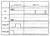
도 20은 전위의 관계를 나타낸 타이밍 차트.
도 21은 반도체 장치를 설명하기 위한 회로도.
도 22는 반도체 장치를 설명하기 위한 단면도 및 평면도.
도 23은 반도체 장치를 설명하기 위한 단면도.
도 24는 반도체 장치를 설명하기 위한 단면도.
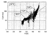
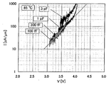
도 25는 산화물 반도체를 이용한 트랜지스터의 특성을 나타낸 도면.
도 26은 산화물 반도체를 이용한 트랜지스터의 특성 평가용 회로도.
도 27은 산화물 반도체를 이용한 트랜지스터의 특성 평가용 타이밍 차트.
도 28은 산화물 반도체를 이용한 트랜지스터의 특성을 나타낸 도면.
도 29는 산화물 반도체를 이용한 트랜지스터의 특성을 나타낸 도면.
도 30은 산화물 반도체를 이용한 트랜지스터의 특성을 나타낸 도면.
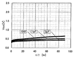
도 31은 메모리창 폭의 조사 결과를 나타낸 도면.1 is a circuit diagram for explaining a semiconductor device;
2 is a cross-sectional view and a plan view for explaining a semiconductor device;
3 is a cross-sectional view illustrating a manufacturing process of a semiconductor device.
4 is a cross-sectional view for explaining a manufacturing process of a semiconductor device.
5 is a cross-sectional view for explaining a manufacturing process of a semiconductor device.
6 is a sectional view for explaining a semiconductor device;
7 is a sectional view for explaining a semiconductor device;
8 is a sectional view for explaining a semiconductor device;
9 is a sectional view for explaining a semiconductor device;
10 is a view for explaining an electronic apparatus using a semiconductor device;
11 is a longitudinal sectional view of a reverse stagger type transistor using an oxide semiconductor.
12 is an energy band diagram (schematic diagram) of the section taken along the line A-A 'in Fig.
13A shows a state in which a positive potential (+ V G ) is given to the gate GE1 and FIG. 13B shows a state in which a negative potential (-V G ).
Fig. 14 is a graph showing the relationship between a vacuum level and a work function? M of a metal and an electron affinity (?) Of an oxide semiconductor.
15 is a circuit diagram for explaining a semiconductor device;
16 is a circuit diagram for explaining a semiconductor device;
17 is a circuit diagram for explaining a semiconductor device;
18 is a circuit diagram for explaining a semiconductor device;
19 is a circuit diagram for explaining a semiconductor device;
20 is a timing chart showing the relationship of potentials;
21 is a circuit diagram for explaining a semiconductor device;
22 is a cross-sectional view and a plan view for explaining a semiconductor device;
23 is a sectional view for explaining a semiconductor device;
24 is a sectional view for explaining a semiconductor device;
25 is a diagram showing the characteristics of a transistor using an oxide semiconductor.
26 is a circuit diagram for evaluating characteristics of a transistor using an oxide semiconductor.
27 is a timing chart for evaluating characteristics of a transistor using an oxide semiconductor.
28 is a diagram showing the characteristics of a transistor using an oxide semiconductor.
29 is a diagram showing the characteristics of a transistor using an oxide semiconductor.
30 is a diagram showing the characteristics of a transistor using an oxide semiconductor.
31 is a view showing a result of investigation of a memory window width;
본 발명의 실시형태의 일례에 대하여, 도면을 이용하여 이하에 설명한다. 단, 본 발명은 이하의 설명에 한정되지 않고, 본 발명의 취지 및 그 범위로부터 벗어나지 않고 그 형태 및 상세한 사항을 다양하게 변경할 수 있다는 것은 당업자라면 용이하게 이해할 수 있다. 따라서, 본 발명은 이하에 나타내는 실시형태의 기재 내용에 한정하여 해석되는 것은 아니다.An example of an embodiment of the present invention will be described below with reference to the drawings. It should be understood, however, by those skilled in the art that the present invention is not limited to the following description, and that various changes in form and details may be made therein without departing from the spirit and scope of the present invention. Therefore, the present invention is not construed as being limited to the description of the embodiments described below.
또한, 도면에서 나타낸 각 구성의 위치, 크기, 범위 등은 이해를 용이하게 하기 위해, 실제의 위치, 크기, 범위 등을 나타내지 않은 경우가 있다. 따라서, 본 발명의 실시형태는 반드시, 도면에 개시된 위치, 크기, 범위 등에 한정되지 않는다.In order to facilitate understanding, the position, size, range, and the like of each constitution shown in the drawings may not represent the actual position, size, range, and the like. Therefore, the embodiments of the present invention are not necessarily limited to the positions, sizes, ranges and the like disclosed in the drawings.
또한, 본 명세서에서 「제 1」, 「제 2」, 「제 3」 등의 서수는 구성 요소의 혼동을 피하기 위해 붙인 것이고, 수적으로 한정하는 것이 아니라는 것을 부기한다.It should be noted that ordinal numbers such as " first, " " second, " and " third, " in the present specification are added to avoid confusion of components, and are not limited to numbers.
(실시형태 1)(Embodiment 1)
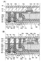
본 실시형태에서는, 개시하는 발명의 일 양태에 관한 반도체 장치의 구성 및 제작 방법에 대하여, 도 1 내지 도 9를 참조하여 설명한다.In this embodiment, a configuration and a manufacturing method of a semiconductor device according to one aspect of the disclosed invention will be described with reference to Figs. 1 to 9. Fig.
<반도체 장치의 회로 구성><Circuit Configuration of Semiconductor Device>
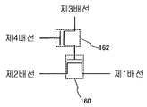
도 1에는, 반도체 장치의 회로 구성의 일례를 나타낸다. 이 반도체 장치는 산화물 반도체 이외의 재료(예를 들면 실리콘)를 이용한 트랜지스터(160)와 산화물 반도체를 이용한 트랜지스터(162)에 의해 구성된다. 또한, 이하에서, 도 1에 나타낸 반도체 장치를 메모리 셀이라고 부르는 경우가 있다.Fig. 1 shows an example of a circuit configuration of a semiconductor device. This semiconductor device comprises a
여기서, 트랜지스터(160)의 게이트 전극과, 트랜지스터(162)의 소스 전극 또는 드레인 전극의 한쪽은 전기적으로 접속되어 있다. 또한, 제 1 배선(1st Line:소스선(SL)이라고도 부름)와 트랜지스터(160)의 소스 전극은 전기적으로 접속되고, 제 2 배선(2nd Line:비트선(BL)이라고도 부름)과 트랜지스터(160)의 드레인 전극은 전기적으로 접속되어 있다. 그리고, 제 3 배선(3rd Line:제 1 신호선(S1)이라고도 부름)과 트랜지스터(162)의 소스 전극 또는 드레인 전극의 다른 한쪽은 전기적으로 접속되고, 제 4 배선(4th Line:제 2 신호선(S2)이라고도 부름)과 트랜지스터(162)의 게이트 전극은 전기적으로 접속되어 있다.Here, the gate electrode of the
산화물 반도체 이외의 재료를 이용한 트랜지스터(160)는 산화물 반도체를 이용한 트랜지스터와 비교하여, 새로운 고속 동작이 가능하기 때문에, 이것을 이용함으로써, 기억 내용의 판독 등을 고속으로 행하는 것이 가능하다. 또한, 산화물 반도체를 이용한 트랜지스터(162)는 오프 전류가 매우 작다는 특징을 가지고 있다. 따라서, 트랜지스터(162)를 오프 상태로 함으로써, 트랜지스터(160)의 게이트 전극의 전위를 매우 장시간에 걸쳐 보유하는 것이 가능하다. 또한, 산화물 반도체를 이용한 트랜지스터(162)에서는 단채널 효과가 나타나기 어렵다는 메리트도 있다.Since the
게이트 전극의 전위를 보유할 수 있다는 특징을 살림으로써, 다음과 같이, 정보의 기입, 보유, 판독이 가능하다.By holding the potential of the gate electrode, it is possible to write, hold and read information as follows.
처음에, 정보의 기입 및 보유에 대하여 설명한다. 먼저, 제 4 배선의 전위를 트랜지스터(162)가 온 상태가 되는 전위로 하여 트랜지스터(162)를 온 상태로 한다. 이것에 의해, 제 3 배선의 전위가 트랜지스터(160)의 게이트 전극에 부여된다(기입). 그 후, 제 4 배선의 전위를 트랜지스터(162)가 오프 상태가 되는 전위로 하여 트랜지스터(162)를 오프 상태로 함으로써, 트랜지스터(160)의 게이트 전극의 전위가 보유된다(보유).Initially, the writing and holding of information will be described. First, the potential of the fourth wiring is set to the potential at which the
트랜지스터(162)의 오프 전류는 매우 작기 때문에, 트랜지스터(160)의 게이트 전극의 전위는 장시간에 걸쳐 보유된다. 예를 들면, 트랜지스터(160)의 게이트 전극의 전위가 트랜지스터(160)를 온 상태로 하는 전위라면, 트랜지스터(160)의 온 상태가 장시간에 걸쳐 보유되게 된다. 또한, 트랜지스터(160)의 게이트 전극의 전위가 트랜지스터(160)를 오프 상태로 하는 전위라면, 트랜지스터(160)의 오프 상태가 장시간에 걸쳐 보유된다.Since the off current of the
다음에, 정보의 판독에 대하여 설명한다. 위에서 설명한 바와 같이, 트랜지스터(160)의 온 상태 또는 오프 상태가 보유된 상태에서, 제 1 배선에 소정의 전위(저전위)가 부여되면, 트랜지스터(160)의 온 상태 또는 오프 상태에 따라, 제 2 배선의 전위는 다른 값을 취한다. 예를 들면, 트랜지스터(160)가 온 상태인 경우에는, 제 1 배선의 전위의 영향을 받아, 제 2 배선의 전위가 저하되게 된다. 반대로, 트랜지스터(160)가 오프 상태인 경우에는, 제 2 배선의 전위는 변화하지 않는다.Next, the reading of information will be described. As described above, when a predetermined potential (low potential) is applied to the first wiring in the ON state or OFF state of the
이와 같이, 정보가 보유된 상태에서, 제 2 배선의 전위를 소정의 전위와 서로 비교함으로써, 정보를 읽어낼 수 있다.As described above, information can be read by comparing the potential of the second wiring with a predetermined potential in a state in which information is held.
다음에, 정보의 다시쓰기에 대하여 설명한다. 정보의 다시쓰기는 상기 정보의 기입 및 보유와 마찬가지로 행해진다. 즉, 제 4 배선의 전위를 트랜지스터(162)가 온 상태가 되는 전위로 하여 트랜지스터(162)를 온 상태로 한다. 이것에 의해, 제 3 배선의 전위(새로운 정보에 관한 전위)가 트랜지스터(160)의 게이트 전극에 부여된다. 그 후, 제 4 배선의 전위를 트랜지스터(162)가 오프 상태가 되는 전위로 하여 트랜지스터(162)를 오프 상태로 함으로써, 새로운 정보가 보유된 상태가 된다.Next, rewriting of information will be described. The rewriting of the information is performed in the same manner as the writing and holding of the information. That is, the potential of the fourth wiring is set to the potential at which the
이와 같이, 개시하는 발명에 관한 반도체 장치는, 재차의 정보의 기입에 의해 직접적으로 정보를 다시쓰는 것이 가능하다. 따라서 플래시 메모리 등에 있어 필요하게 되는 소거 동작이 불필요하고, 소거 동작에 기인하는 동작 속도의 저하를 억제할 수 있다. 즉, 반도체 장치의 고속 동작이 실현된다.Thus, the semiconductor device according to the disclosed invention can rewrite information directly by rewriting the information. Therefore, the erase operation required for the flash memory or the like is unnecessary, and the lowering of the operation speed due to the erase operation can be suppressed. That is, a high-speed operation of the semiconductor device is realized.
산화물 반도체를 이용한 기입용 트랜지스터(162)의 오프 전류는 매우 작고, 트랜지스터(160)의 게이트 전극의 전위는 장시간에 걸쳐서 보유된다. 따라서, 예를 들면, 종래의 DRAM에서 필요한 리프레시 동작이 불필요해지거나, 또는, 리프레시 동작의 빈도를 매우 낮게(예를 들면, 1개월∼일년에 1회 정도) 하는 것이 가능하다. 이와 같이, 개시하는 발명의 반도체 장치는 실질적인 불휘발성 기억 장치로서의 특징을 구비하고 있다.The off current of the
또한, 개시하는 발명의 반도체 장치는 종래의 DRAM과는 달리, 판독에 의해 정보가 사라지는 일이 없기 때문에, 판독할 때마다 다시 정보를 기입할 필요도 없다. 이와 같이, DRAM과 비교하여 정보의 기입의 빈도를 현저하게 저감할 수 있기 때문에, 소비 전력을 충분히 억제하는 것이 가능하다.Further, unlike the conventional DRAM, the semiconductor device of the disclosed invention does not lose information due to reading, and therefore, there is no need to write information again every time it is read. As described above, since the frequency of writing information can be remarkably reduced as compared with the DRAM, the power consumption can be sufficiently suppressed.
또한, 개시하는 발명의 반도체 장치는 반도체 장치에 다시 정보의 기입을 함으로써 직접적으로 정보를 다시쓰는 것이 가능하다. 따라서 플래시 메모리 등에서 필요하게 되는 소거 동작이 불필요하고, 소거 동작에 기인하는 동작 속도의 저하를 억제할 수 있다. 즉, 반도체 장치의 고속 동작이 실현된다. 또한, 종래의 플로팅 게이트형 트랜지스터로의 정보의 기입이나 소거 시에 필요한 높은 전압을 필요로 하지 않기 때문에, 반도체 장치의 소비 전력을 더욱 저감할 수 있다.In addition, the semiconductor device of the disclosed invention is capable of directly rewriting information by writing information again to the semiconductor device. Therefore, the erasing operation required in the flash memory or the like is not required, and the lowering of the operating speed due to the erasing operation can be suppressed. That is, a high-speed operation of the semiconductor device is realized. In addition, since a high voltage required for writing or erasing information in the conventional floating gate type transistor is not required, the power consumption of the semiconductor device can be further reduced.
또한, 개시하는 발명에 관한 반도체 장치는 기입용 트랜지스터와 판독용 트랜지스터를 적어도 포함하고 있으면 좋고, 1 메모리 셀당 6개의 트랜지스터를 필요로 하는 SRAM 등과 비교하여, 메모리 셀당의 면적을 충분히 작게 하는 것이 가능하다. 따라서, 반도체 장치를 고밀도로 배치할 수 있다.Further, the semiconductor device according to the disclosed invention may include at least the write transistor and the read transistor, and it is possible to sufficiently reduce the area per memory cell as compared with the SRAM or the like which requires six transistors per memory cell . Therefore, the semiconductor device can be arranged at a high density.
또한, 종래의 플로팅 게이트형 트랜지스터에서는 기입시에 게이트 절연막(터널 절연막) 중을 전하가 이동하기 때문에, 이 게이트 절연막(터널 절연막)의 열화가 불가피했다. 그러나, 본 발명의 일 양태에 관한 메모리 셀에서는, 기입용 트랜지스터의 스위칭 동작에 의해 정보의 기입이 이루어지기 때문에, 종래 문제였던 게이트 절연막의 열화를 해소할 수 있다. 이것은, 원리적인 기입 횟수의 제한이 존재하지 않고, 다시쓰기 내성이 매우 높은 것을 의미하는 것이다. 예를 들면, 1×10⁹회(10억회) 이상의 기입 후에도, 전류-전압 특성에 열화가 보여지지 않는다.In addition, in the conventional floating gate type transistor, since charge moves in the gate insulating film (tunnel insulating film) at the time of writing, deterioration of the gate insulating film (tunnel insulating film) is inevitable. However, in the memory cell according to one aspect of the present invention, since information is written by the switching operation of the writing transistor, deterioration of the gate insulating film, which has been a conventional problem, can be solved. This means that there is no limitation on the number of the basic writing, and the rewriting resistance is very high. For example, no deterioration in the current-voltage characteristic is observed even after writing of 1 x 10 9 (1 billion cycles) or more.
또한, 산화물 반도체를 이용한 기입용 트랜지스터(162)의 전계 효과 이동도는 온 상태에서, 3 cm2/Vs 이상 250 cm2/Vs 이하, 바람직하게는 5 cm2/Vs 이상 200 cm2/Vs 이하, 보다 바람직하게는 10 cm2/Vs 이상 150 cm2/Vs 이하로 한다. 또한, 산화물 반도체를 이용한 트랜지스터는 서브스레숄드 스윙값(S값)이 0.1 V/dec. 이하가 되도록 한다. 이러한 트랜지스터를 이용함으로써, 정보의 기입에 필요한 시간을 충분히 짧게 할 수 있다.The field effect mobility of the
또한, 산화물 반도체를 이용한 기입용 트랜지스터(162)의 채널 길이(L)는 10 nm 이상 400 nm 이하로 하는 것이 바람직하다. 이러한 채널 사이즈로 함으로써, 트랜지스터의 동작의 고속화, 저소비 전력화, 고집적화 등, 여러 가지 효과를 얻을 수 있다.The channel length L of the
또한, 판독용 트랜지스터(160)에는, 결정성의 실리콘을 이용한 트랜지스터를 적용하는 것이 바람직하다. 특히, 판독 동작의 고속화의 관점에서는 단결정 실리콘을 이용한 n 채널형의 트랜지스터를 이용하는 것이 좋다. 이러한 단결정 실리콘 트랜지스터는 예를 들면, 벌크 실리콘(소위 실리콘 웨이퍼)을 이용하여 형성할 수 있다.It is preferable to apply a transistor using crystalline silicon to the
또한, 상기 설명은 n형 트랜지스터(n 채널형 트랜지스터)를 이용하는 경우에 대한 것이지만, n형 트랜지스터 대신에, p형 트랜지스터를 이용할 수 있다는 것은 말할 필요도 없다.Note that the above description is for the case of using an n-type transistor (n-channel transistor), but it goes without saying that a p-type transistor can be used instead of the n-type transistor.
<반도체 장치의 평면 구성 및 단면 구성><Planar Configuration and Sectional Configuration of Semiconductor Device>
도 2는 상기 반도체 장치의 구성의 일례이다. 도 2의 (A)에는 반도체 장치의 단면을, 도 2의 (B)에는 반도체 장치의 평면을 각각 나타낸다. 여기서, 도 2(A)는 도 2의 (B)의 선 A1-A2 및 선 B1-B2에서의 단면에 상당한다. 도 2의 (A) 및 도 2의 (B)에 나타낸 반도체 장치는 하부에 산화물 반도체 이외의 재료를 이용한 트랜지스터(160)를 가지고, 상부에 산화물 반도체를 이용한 트랜지스터(162)를 가지는 것이다. 또한, 트랜지스터(160) 및 트랜지스터(162)는 모두 n형 트랜지스터로서 설명하지만, p형 트랜지스터를 채용해도 좋다. 특히, 트랜지스터(160)는 p형으로 하는 것이 용이하다.2 is an example of the configuration of the semiconductor device. FIG. 2A shows a cross section of the semiconductor device, and FIG. 2B shows the plane of the semiconductor device. Here, FIG. 2A corresponds to a cross section taken along line A1-A2 and line B1-B2 in FIG. 2B. The semiconductor device shown in Figs. 2A and 2B has a
트랜지스터(160)는 반도체 재료를 포함하는 기판(100)에 형성된 채널 형성 영역(116)과 채널 형성 영역(116)을 끼우도록 형성된 불순물 영역(114) 및 고농도 불순물 영역(120)(이것들을 아울러 간단히 불순물 영역이라고도 부름)과, 채널 형성 영역(116) 위에 형성된 게이트 절연층(108)과, 게이트 절연층(108) 위에 형성된 게이트 전극(110)과, 불순물 영역(114)과 전기적으로 접속하는 소스 전극 또는 드레인 전극(130a), 소스 전극 또는 드레인 전극(130b)을 가진다.The
여기서, 게이트 전극(110)의 측면에는 사이드 월 절연층(118)이 형성되어 있다. 또한, 기판(100)의 단면도에 나타낸 바와 같이, 사이드 월 절연층(118)과 겹치지 않는 영역에는 고농도 불순물 영역(120)을 가지고, 고농도 불순물 영역(120) 위에는 금속 화합물 영역(124)이 존재한다. 또한, 기판(100) 위에는 트랜지스터(160)를 둘러싸도록 소자 분리 절연층(106)이 형성되어 있고, 트랜지스터(160)를 덮도록, 층간 절연층(126) 및 층간 절연층(128)이 형성되어 있다. 소스 전극 또는 드레인 전극(130a), 소스 전극 또는 드레인 전극(130b)은 층간 절연층(126) 및 층간 절연층(128)에 형성된 개구를 통하여, 금속 화합물 영역(124)과 전기적으로 접속되어 있다. 즉, 소스 전극 또는 드레인 전극(130a), 소스 전극 또는 드레인 전극(130b)은 금속 화합물 영역(124)을 통하여 고농도 불순물 영역(120) 및 불순물 영역(114)과 전기적으로 접속되어 있다. 또한, 게이트 전극(110)에는 소스 전극 또는 드레인 전극(130a)이나 소스 전극 또는 드레인 전극(130b)과 마찬가지로 형성된 전극(130c)이 전기적으로 접속되어 있다.A
트랜지스터(162)는 층간 절연층(128) 위에 형성된 게이트 전극(136d)과, 게이트 전극(136d) 위에 형성된 게이트 절연층(138)과, 게이트 절연층(138) 위에 형성된 산화물 반도체층(140)과, 산화물 반도체층(140) 위에 형성되고, 산화물 반도체층(140)과 전기적으로 접속되어 있는 소스 전극 또는 드레인 전극(142a), 소스 전극 또는 드레인 전극(142b)을 가진다.The
여기서, 게이트 전극(136d)은 층간 절연층(128) 위에 형성된 절연층(132)에 묻히도록 형성되어 있다. 또한, 게이트 전극(136d)과 마찬가지로, 소스 전극 또는 드레인 전극(130a)에 접하여 전극(136a)이, 소스 전극 또는 드레인 전극(130b)에 접하여 전극(136b)이, 전극(130c)에 접하여 전극(136c)이, 각각 형성되어 있다.Here, the
또한, 트랜지스터(162)의 위에는, 산화물 반도체층(140)의 일부와 접하도록 보호 절연층(144)이 형성되어 있고, 보호 절연층(144) 위에는 층간 절연층(146)이 형성되어 있다. 여기서, 보호 절연층(144) 및 층간 절연층(146)에는 소스 전극 또는 드레인 전극(142a), 소스 전극 또는 드레인 전극(142b)에까지 달하는 개구가 형성되어 있고, 이 개구를 통하여, 전극(150d), 전극(150e)이 소스 전극 또는 드레인 전극(142a), 소스 전극 또는 드레인 전극(142b)에 접하여 형성되어 있다. 또한, 전극(150d), 전극(150e)과 마찬가지로, 게이트 절연층(138), 보호 절연층(144), 층간 절연층(146)에 형성된 개구를 통하여, 전극(136a), 전극(136b), 전극(136c)에 접하는 전극(150a), 전극(150b), 전극(150c)이 형성되어 있다.A protective insulating
여기서, 산화물 반도체층(140)은 수소 등의 불순물이 충분히 제거되어, 고순도화되어 있는 것인 것이 바람직하다. 구체적으로는, 산화물 반도체층(140)의 수소 농도는 5×10¹⁹ atoms/cm3 이하, 바람직하게는 5×10¹⁸ atoms/cm3 이하, 보다 바람직하게는 5×10¹⁷ atoms/cm3 이하로 한다. 이것에 의해, 일반적인 실리콘 웨이퍼(인이나 붕소 등의 불순물 원소가 미량으로 첨가된 실리콘 웨이퍼)에서의 캐리어 농도(1×10¹⁴/cm3 정도)와 비교하여, 충분히 작은 캐리어 농도의 값(예를 들면, 1×10¹²/cm3 미만, 혹은, 1.45×10¹⁰/cm3 미만)이 된다. 이와 같이, 수소 농도가 충분히 저감되어 고순도화되고, 진성화(i형화) 또는 실질적으로 진성화(i형화)된 산화물 반도체를 이용함으로써, 매우 뛰어난 오프 전류 특성의 트랜지스터(162)를 얻을 수 있다. 예를 들면, 트랜지스터(162)의 실온(25℃)에서의 오프 전류(여기에서는, 단위 채널폭(1μm)당의 값)은 10 zA/μm(1 zA(젭토 암페어)는 1×10- 21 A) 이하, 바람직하게는, 1 zA/μm 이하가 된다. 또한, 85℃에서 트랜지스터(162)의 오프 전류는, 100 zA/μm(1×10- 19 A/μm) 이하, 바람직하게는 10 zA/μm(1×10- 20 A/μm) 이하가 된다. 이와 같이, 수소 농도가 충분히 저감되어 진성화 또는 실질적으로 진성화된 산화물 반도체층(140)을 적용하여, 트랜지스터(162)의 오프 전류를 저감함으로써, 새로운 구성의 반도체 장치를 실현할 수 있다. 또한, 상술한 산화물 반도체층(140) 중의 수소 농도는 2차 이온 질량분석법(SIMS:Secondary Ion Mass Spectrometry)으로 측정한 것이다.Here, it is preferable that the
또한, 층간 절연층(146) 위에는 절연층(152)이 형성되어 있고, 이 절연층(152)에 묻히도록, 전극(154a), 전극(154b), 전극(154c), 전극(154d)이 형성되어 있다. 여기서, 전극(154a)은 전극(150a)과 접하고 있고, 전극(154b)은 전극(150b)과 접하고 있고, 전극(154c)은 전극(150c) 및 전극(150d)과 접하고 있고, 전극(154d)은 전극(150e)과 접하고 있다.An
즉, 도 2에 나타낸 반도체 장치에서는, 트랜지스터(160)의 게이트 전극(110)과, 트랜지스터(162)의 소스 전극 또는 드레인 전극(142a)이 전극(130c), 전극(136c), 전극(150c), 전극(154c) 및 전극(150d)을 통하여 전기적으로 접속되어 있다.2, the
<반도체 장치의 제작 방법><Manufacturing Method of Semiconductor Device>
다음에, 상기 반도체 장치의 제작 방법의 일례에 대하여 설명한다. 이하에서는, 처음에 하부의 트랜지스터(160)의 제작 방법에 대하여 도 3을 참조하여 설명하고, 그 후, 상부의 트랜지스터(162)의 제작 방법에 대하여 도 4 및 도 5를 참조하여 설명한다.Next, an example of a manufacturing method of the semiconductor device will be described. Hereinafter, a method of manufacturing the
<하부의 트랜지스터의 제작 방법>≪ Method of fabricating lower transistor &
먼저, 반도체 재료를 포함하는 기판(100)을 준비한다(도 3의 (A) 참조). 반도체 재료를 포함하는 기판(100)으로서는, 실리콘이나 탄화실리콘 등의 단결정 반도체 기판, 다결정 반도체 기판, 실리콘 게르마늄 등의 화합물 반도체 기판, SOI 기판 등을 적용할 수 있다. 여기에서는, 반도체 재료를 포함하는 기판(100)으로서, 단결정 실리콘 기판을 이용하는 경우의 일례에 대하여 나타내는 것으로 한다.First, a
기판(100) 위에는, 소자 분리 절연층을 형성하기 위한 마스크가 되는 보호층(102)을 형성한다(도 3의 (A) 참조). 보호층(102)으로서는, 예를 들면, 산화실리콘이나 질화실리콘, 질화산화실리콘 등을 재료로 하는 절연층을 이용할 수 있다. 또한, 이 공정의 전후에 있어서, 트랜지스터의 스레숄드 전압을 제어하기 위해, n형의 도전성을 부여하는 불순물 원소나 p형의 도전성을 부여하는 불순물 원소를 기판(100)에 첨가해도 좋다. 반도체가 실리콘인 경우, n형의 도전성을 부여하는 불순물로서는, 예를 들면, 인이나 비소 등을 이용할 수 있다. 또한, p형의 도전성을 부여하는 불순물로서는, 예를 들면, 붕소, 알루미늄, 갈륨 등을 이용할 수 있다.On the
다음에, 상기의 보호층(102)을 마스크로서 에칭을 행하고, 보호층(102)으로 덮이지 않은 영역(노출되어 있는 영역)의 기판(100)의 일부를 제거한다. 이것에 의해 분리된 반도체 영역(104)이 형성된다(도 3의 (B) 참조). 이 에칭에는 드라이 에칭을 이용하는 것이 적합하지만, 웨트 에칭을 이용해도 좋다. 에칭 가스나 에칭액에 대해서는 피에칭 재료에 따라 적절히 선택할 수 있다.Next, etching is performed using the
다음에, 반도체 영역(104)을 덮도록 절연층을 형성하고, 반도체 영역(104)에 중첩하는 영역의 절연층을 선택적으로 제거함으로써, 소자 분리 절연층(106)을 형성한다(도 3의 (B) 참조). 이 절연층은 산화실리콘이나 질화실리콘, 질화산화실리콘 등을 이용하여 형성된다. 절연층의 제거 방법으로서는, CMP 등의 연마 처리나 에칭 처리 등이 있지만, 그 중 어느 것을 이용해도 좋다. 또한, 반도체 영역(104)의 형성 후, 또는, 소자 분리 절연층(106)의 형성 후에는, 상기 보호층(102)을 제거한다.Next, an insulating layer is formed so as to cover the
다음에, 반도체 영역(104) 위에 절연층을 형성하고, 이 절연층 위에 도전 재료를 포함하는 층을 형성한다.Next, an insulating layer is formed on the
절연층은 후의 게이트 절연층이 되는 것으로서, CVD법이나 스퍼터링법 등을 이용하여 얻어지는 산화실리콘, 질화산화실리콘, 질화실리콘, 산화하프늄, 산화알루미늄, 산화탄탈 등을 포함하는 막의 단층 구조 또는 적층 구조로 하면 좋다. 그 밖에, 고밀도 플라즈마 처리나 열산화 처리에 의해, 반도체 영역(104)의 표면을 산화, 질화시킴으로써, 상기 절연층을 형성해도 좋다. 고밀도 플라즈마 처리는, 예를 들면, He, Ar, Kr, Xe 등의 희가스와, 산소, 산화질소, 암모니아, 질소, 수소 등의 혼합 가스를 이용하여 행할 수 있다. 또한, 절연층의 두께는 특별히 한정되지 않지만, 예를 들면, 1 nm 이상 100 nm 이하로 할 수 있다.The insulating layer serves as a later gate insulating layer and may be a single layer structure or a laminated structure of a film containing silicon oxide, silicon nitride oxide, silicon nitride, hafnium oxide, aluminum oxide, tantalum oxide, or the like obtained by a CVD method or a sputtering method It is good. Alternatively, the insulating layer may be formed by oxidizing and nitriding the surface of the
도전 재료를 포함하는 층은 알루미늄이나 구리, 티탄, 탄탈, 텅스텐 등의 금속 재료를 이용하여 형성할 수 있다. 또한, 도전 재료를 포함하는 다결정 실리콘 등의 반도체 재료를 이용하여, 도전 재료를 포함하는 층을 형성해도 좋다. 형성 방법도 특별히 한정되지 않고, 증착법, CVD법, 스퍼터링법, 스핀 코트법 등의 각종 성막 방법을 이용할 수 있다. 또한, 본 실시형태에서는, 도전 재료를 포함하는 층을, 금속 재료를 이용하여 형성하는 경우의 일례에 대하여 나타내는 것으로 한다.The layer containing the conductive material can be formed using a metal material such as aluminum, copper, titanium, tantalum, or tungsten. Further, a layer containing a conductive material may be formed using a semiconductor material such as polycrystalline silicon containing a conductive material. The forming method is not particularly limited, and various film forming methods such as a vapor deposition method, a CVD method, a sputtering method, and a spin coating method can be used. In the present embodiment, an example in which a layer containing a conductive material is formed using a metal material is shown.
그 후, 절연층 및 도전 재료를 포함하는 층을 선택적으로 에칭하여, 게이트 절연층(108), 게이트 전극(110)을 형성한다(도 3의 (C) 참조).Thereafter, the insulating layer and the layer including the conductive material are selectively etched to form the
다음에, 게이트 전극(110)을 덮는 절연층(112)을 형성한다(도 3의 (C) 참조). 그리고, 반도체 영역(104)에 인(P)이나 비소(As) 등을 첨가하여, 기판(100)과의 얕은 접합 깊이의 불순물 영역(114)을 형성한다(도 3의 (C) 참조). 또한, 여기에서는 n형 트랜지스터를 형성하기 위해 인이나 비소를 첨가하고 있지만, p형 트랜지스터를 형성하는 경우에는, 붕소(B)나 알루미늄(Al) 등의 불순물 원소를 첨가하면 좋다. 또한, 불순물 영역(114)의 형성에 의해, 반도체 영역(104)의 게이트 절연층(108) 하부에는 채널 형성 영역(116)이 형성된다(도 3의 (C) 참조). 여기서, 첨가하는 불순물의 농도는 적절히 설정할 수 있지만, 반도체 소자가 고도로 미세화되는 경우에는, 그 농도를 높게 하는 것이 바람직하다. 또한, 여기에서는, 절연층(112)을 형성한 후에 불순물 영역(114)을 형성하는 공정을 채용하고 있지만, 불순물 영역(114)을 형성한 후에 절연층(112)을 형성하는 공정으로 해도 좋다.Next, an insulating
다음에, 사이드 월 절연층(118)을 형성한다(도 3의 (D) 참조). 사이드 월 절연층(118)은 절연층(112)을 덮도록 절연층을 형성한 후에, 이 절연층에 이방성이 높은 에칭 처리를 적용함으로써, 자기 정합적으로 형성할 수 있다. 또한, 이때, 절연층(112)을 부분적으로 에칭하여, 게이트 전극(110)의 상면과, 불순물 영역(114)의 상면을 노출시키면 좋다.Next, a
다음에, 게이트 전극(110), 불순물 영역(114), 사이드 월 절연층(118) 등을 덮도록 절연층을 형성한다. 그리고, 이 절연층이 불순물 영역(114)과 접하는 영역에, 인(P)이나 비소(As) 등을 첨가하여, 고농도 불순물 영역(120)을 형성한다(도 3의 (E) 참조). 그 후, 상기 절연층을 제거하고, 게이트 전극(110), 사이드 월 절연층(118), 고농도 불순물 영역(120) 등을 덮도록 금속층(122)을 형성한다(도 3의 (E) 참조). 이 금속층(122)은 진공 증착법이나 스퍼터링법, 스핀 코트법 등의 각종 성막 방법을 이용하여 형성할 수 있다. 금속층(122)은 반도체 영역(104)을 구성하는 반도체 재료와 반응하여 저저항의 금속 화합물이 되는 금속 재료를 이용하여 형성하는 것이 바람직하다. 이러한 금속 재료로서는, 예를 들면, 티탄, 탄탈, 텅스텐, 니켈, 코발트, 백금 등이 있다.Next, an insulating layer is formed to cover the
다음에, 열처리를 실시하여, 상기 금속층(122)과 반도체 재료를 반응시킨다. 이것에 의해, 고농도 불순물 영역(120)에 접하는 금속 화합물 영역(124)이 형성된다(도 3(F) 참조). 또한, 게이트 전극(110)으로서 다결정 실리콘 등을 이용하는 경우에는, 게이트 전극(110)의 금속층(122)과 접촉하는 부분에도, 금속 화합물 영역이 형성되게 된다.Next, a heat treatment is performed to cause the
상기 열처리로서는, 예를 들면, 플래시 램프의 조사에 의한 열처리를 이용할 수 있다. 물론, 그 외의 열처리 방법을 이용해도 좋지만, 금속 화합물의 형성에 관한 화학 반응의 제어성을 향상시키기 위해서는, 극히 단시간의 열처리를 실현될 수 있는 방법을 이용하는 것이 바람직하다. 또한, 상기의 금속 화합물 영역은 금속 재료와 반도체 재료와의 반응에 의해 형성되는 것이고, 충분히 도전성이 높여진 영역이다. 이 금속 화합물 영역을 형성함으로써, 전기 저항을 충분히 저감하여, 소자 특성을 향상시킬 수 있다. 또한, 금속 화합물 영역(124)을 형성한 후에는, 금속층(122)은 제거한다.As the heat treatment, for example, heat treatment by irradiation with a flash lamp can be used. Of course, other heat treatment methods may be used. However, in order to improve the controllability of the chemical reaction related to the formation of the metal compound, it is preferable to use a method capable of realizing an extremely short time heat treatment. The metal compound region is formed by reaction between a metal material and a semiconductor material, and is a region in which conductivity is sufficiently enhanced. By forming this metal compound region, it is possible to sufficiently reduce the electrical resistance and improve the device characteristics. Further, after the
다음에, 상술한 공정에 의해 형성된 각 구성을 덮도록, 층간 절연층(126), 층간 절연층(128)을 형성한다(도 3의 (G) 참조). 층간 절연층(126)이나 층간 절연층(128)은 산화실리콘, 질화산화실리콘, 질화실리콘, 산화하프늄, 산화알루미늄, 산화탄탈 등의 무기 절연 재료를 포함하는 재료를 이용하여 형성할 수 있다. 또한, 폴리이미드, 아크릴 수지 등의 유기 절연 재료를 이용하여 형성하는 것도 가능하다. 또한, 여기에서는, 층간 절연층(126)과 층간 절연층(128)의 2층 구조로 하고 있지만, 층간 절연층의 구성은 이것에 한정되지 않는다. 층간 절연층(128)의 형성 후에는, 그 표면을 CMP나 에칭 처리 등에 의해 평탄화해 두는 것이 바람직하다.Next, an
그 후, 상기 층간 절연층(126, 128)에 금속 화합물 영역(124)에까지 달하는 개구를 형성하고, 이 개구에 소스 전극 또는 드레인 전극(130a), 소스 전극 또는 드레인 전극(130b)을 형성한다(도 3의 (H) 참조). 소스 전극 또는 드레인 전극(130a)이나 소스 전극 또는 드레인 전극(130b)은 예를 들면, 개구를 포함하는 영역에 PVD법이나 CVD법 등을 이용하여 도전층을 형성한 후, 에칭 처리나 CMP와 같은 방법을 이용하여, 상기 도전층의 일부를 제거함으로써 형성할 수 있다.Thereafter, an opening reaching the
또한, 상기 도전층의 일부를 제거하여 소스 전극 또는 드레인 전극(130a)이나 소스 전극 또는 드레인 전극(130b)을 형성할 때에는, 그 표면이 평탄하게 되도록 가공하는 것이 바람직하다. 예를 들면, 개구를 포함하는 영역에 티탄막이나 질화티탄막을 얇게 형성한 후에, 개구에 묻도록 텅스텐막을 형성하는 경우에는, 그 후의 CMP에 의해, 불필요한 텅스텐막, 티탄막, 질화티탄막 등을 제거함과 동시에, 그 표면의 평탄성을 향상시킬 수 있다. 이와 같이, 소스 전극 또는 드레인 전극(130a), 소스 전극 또는 드레인 전극(130b)을 포함하는 표면을 평탄화함으로써, 후의 공정에서, 양호한 전극, 배선, 절연층, 반도체층 등을 형성하는 것이 가능하게 된다.When the source electrode or the
또한, 여기에서는, 금속 화합물 영역(124)과 접촉하는 소스 전극 또는 드레인 전극(130a)이나 소스 전극 또는 드레인 전극(130b)만을 나타내고 있지만, 이 공정에서, 게이트 전극(110)과 접촉하는 전극(예를 들면, 도 2에서의 전극(130c)) 등을 아울러 형성할 수 있다. 소스 전극 또는 드레인 전극(130a), 소스 전극 또는 드레인 전극(130b)으로서 이용할 수 있는 재료에 대하여 특별히 한정은 없고, 각종 도전 재료를 이용할 수 있다. 예를 들면, 몰리브덴, 티탄, 크롬, 탄탈, 텅스텐, 알루미늄, 구리, 네오디뮴, 스칸듐 등의 도전성 재료를 이용할 수 있다.Here, only the source electrode or the
이상에 의해, 반도체 재료를 포함하는 기판(100)을 이용한 트랜지스터(160)가 형성된다. 또한, 상기 공정 후에는, 전극이나 배선, 절연층 등을 더 형성해도 좋다. 배선의 구조로서 층간 절연층 및 도전층의 적층 구조로 이루어지는 다층 배선 구조를 채용함으로써, 고도로 집적화한 반도체 장치를 제공할 수 있다.Thus, the
<상부의 트랜지스터의 제작 방법>≪ Manufacturing method of upper transistor >
다음에, 도 4 및 도 5를 이용하여, 층간 절연층(128) 위에 트랜지스터(162)를 제작하는 공정에 대하여 설명한다. 또한, 도 4 및 도 5는 층간 절연층(128) 위의 각종 전극이나, 트랜지스터(162) 등의 제작 공정을 나타내는 것이기 때문에, 트랜지스터(162)의 하부에 존재하는 트랜지스터(160) 등에 대해서는 생략한다.Next, a process of manufacturing the
먼저, 층간 절연층(128), 소스 전극 또는 드레인 전극(130a), 소스 전극 또는 드레인 전극(130b), 전극(130c) 위에 절연층(132)을 형성한다(도 4의 (A) 참조). 절연층(132)은 PVD법이나 CVD법 등을 이용하여 형성할 수 있다. 또한, 산화실리콘, 질화산화실리콘, 질화실리콘, 산화하프늄, 산화알루미늄, 산화탄탈 등의 무기 절연 재료를 포함하는 재료를 이용하여 형성할 수 있다.First, an insulating
다음에, 절연층(132)에 대하여, 소스 전극 또는 드레인 전극(130a), 소스 전극 또는 드레인 전극(130b), 및 전극(130c)에까지 달하는 개구를 형성한다. 이때, 후에 게이트 전극(136d)이 형성되는 영역에도 아울러 개구를 형성한다. 그리고, 상기 개구에 묻도록, 도전층(134)을 형성한다(도 4의 (B) 참조). 상기 개구는 마스크를 이용한 에칭 등의 방법으로 형성할 수 있다. 이 마스크는 포토마스크를 이용한 노광 등의 방법에 의해 형성하는 것이 가능하다. 에칭으로서는, 웨트 에칭, 드라이 에칭의 어느 것을 이용해도 좋지만, 미세 가공의 관점에서는, 드라이 에칭을 이용하는 것이 적합하다. 도전층(134)의 형성은 PVD법이나 CVD법 등의 성막법을 이용하여 행할 수 있다. 도전층(134)의 형성에 이용할 수 있는 재료로서는, 몰리브덴, 티탄, 크롬, 탄탈, 텅스텐, 알루미늄, 구리, 네오디뮴, 스칸듐 등의 도전성 재료나, 이들의 합금, 화합물(예를 들면 질화물) 등을 들 수 있다.Next, an opening reaching the source electrode or the
보다 구체적으로는, 예를 들면, 개구를 포함하는 영역에 PVD법에 의해 티탄막을 얇게 형성하고, CVD법에 의해 질화티탄막을 얇게 형성한 후에, 개구에 묻도록 텅스텐막을 형성하는 방법을 적용할 수 있다. 여기서, PVD법에 의해 형성되는 티탄막은 하부 전극(여기에서는 소스 전극 또는 드레인 전극(130a), 소스 전극 또는 드레인 전극(130b), 전극(130c) 등)의 표면의 산화막을 환원하여, 하부 전극과의 접촉 저항을 저감시키는 기능을 가진다. 또한, 그 후에 형성되는 질화티탄막은 도전성 재료의 확산을 억제하는 배리어 기능을 구비한다. 또한, 티탄이나, 질화티탄 등에 의한 배리어막을 형성한 후에, 도금법에 의해 구리막을 형성해도 좋다.More specifically, for example, a method in which a titanium film is formed thinly by a PVD method in an area including an opening, a titanium nitride film is formed thinly by a CVD method, and then a tungsten film is formed so as to be in contact with the opening have. Here, the titanium film formed by the PVD method is formed by reducing the oxide film on the surface of the lower electrode (here, the source electrode or the
도전층(134)을 형성한 후에는, 에칭 처리나 CMP와 같은 방법을 이용하여 도전층(134)의 일부를 제거하여, 절연층(132)을 노출시키고, 전극(136a), 전극(136b), 전극(136c), 게이트 전극(136d)을 형성한다(도 4의 (C) 참조). 또한, 상기 도전층(134)의 일부를 제거하여 전극(136a), 전극(136b), 전극(136c), 게이트 전극(136d)을 형성할 때에는, 표면이 평탄하게 되도록 가공하는 것이 바람직하다. 이와 같이, 절연층(132), 전극(136a), 전극(136b), 전극(136c), 게이트 전극(136d)의 표면을 평탄화함으로써, 후의 공정에서, 양호한 전극, 배선, 절연층, 반도체층 등을 형성하는 것이 가능하게 된다.After the
다음에, 절연층(132), 전극(136a), 전극(136b), 전극(136c), 게이트 전극(136d)을 덮도록, 게이트 절연층(138)을 형성한다(도 4의 (D) 참조). 게이트 절연층(138)은 CVD법이나 스퍼터링법 등을 이용하여 형성할 수 있다. 또한, 게이트 절연층(138)은 산화규소, 질화규소, 산화질화규소, 질화산화규소, 산화알루미늄, 산화하프늄, 산화탄탈 등을 포함하도록 형성하는 것이 적합하다. 또한, 게이트 절연층(138)은 단층 구조로 해도 좋고, 적층 구조로 해도 좋다. 예를 들면, 원료 가스로서 실란(SiH4), 산소, 질소를 이용한 플라즈마 CVD법에 의해, 산화질화규소로 이루어지는 게이트 절연층(138)을 형성할 수 있다. 게이트 절연층(138)의 두께는 특별히 한정되지 않지만, 예를 들면, 10 nm 이상 500 nm 이하로 할 수 있다. 적층 구조의 경우는, 예를 들면, 막두께 50 nm 이상 200 nm 이하의 제 1 게이트 절연층과, 제 1 게이트 절연층 위의 막두께 5 nm 이상 300 nm 이하의 제 2 게이트 절연층의 적층으로 하면 적합하다.Next, a
또한, 불순물을 제거함으로써 i형화 또는 실질적으로 i형화된 산화물 반도체(고순도화된 산화물 반도체)는, 계면 준위나 계면 전하에 대하여 매우 민감하기 때문에, 이러한 산화물 반도체를 산화물 반도체층에 이용하는 경우에는, 게이트 절연층과의 계면은 중요하다. 즉, 고순도화된 산화물 반도체층에 접하는 게이트 절연층(138)에는 고품질화가 요구되게 된다.Further, since the oxide semiconductor (highly purified oxide semiconductors) that is i-type or substantially i-shaped by removing the impurities is very sensitive to the interface level and the interface charge, when such an oxide semiconductor is used for the oxide semiconductor layer, The interface with the insulating layer is important. That is, the quality of the
예를 들면, μ파(2.45 GHz)를 이용한 고밀도 플라즈마 CVD법은 치밀하고 절연 내압이 높은 고품질의 게이트 절연층(138)을 형성할 수 있는 점에서 적합하다. 고순도화된 산화물 반도체층과 고품질 게이트 절연층이 접함으로써, 계면 준위를 저감하여 계면 특성을 양호한 것으로 할 수 있기 때문이다.For example, the high-density plasma CVD method using a microwave (2.45 GHz) is suitable in that it can form a high-quality
물론, 게이트 절연층으로서 양질의 절연층을 형성할 수 있는 것이면, 고순도화된 산화물 반도체층을 이용하는 경우에도, 스퍼터링법이나 플라즈마 CVD법 등 다른 방법을 적용할 수 있다. 또한, 형성 후의 열처리에 의해, 막질이나 산화물 반도체층과의 계면 특성이 개질되는 절연층을 적용해도 좋다. 어쨌든, 게이트 절연층(138)으로서의 막질이 양호함과 동시에, 산화물 반도체층과의 계면 준위 밀도를 저감하여, 양호한 계면을 형성할 수 있는 것을 형성하면 좋다.Of course, if a high-quality insulating layer can be formed as the gate insulating layer, another method such as sputtering or plasma CVD can be applied even when a high-purity oxide semiconductor layer is used. An insulating layer may be used in which the interface property with the film quality or the oxide semiconductor layer is modified by heat treatment after formation. In any case, it is preferable that the film quality as the
불순물이 산화물 반도체에 포함되어 있는 경우, 강한 전계나 높은 온도 등의 스트레스에 의해, 불순물과 산화물 반도체의 주성분과의 결합이 절단되고, 생성된 미결합손은 스레숄드 전압(Vth)의 시프트를 유발한다.When the impurity is contained in the oxide semiconductor, the bond between the impurity and the main component of the oxide semiconductor is broken due to stress such as a strong electric field or a high temperature, and the generated unbonded hand causes a shift of the threshold voltage Vth .
산화물 반도체의 불순물, 특히 수소나 물 등의 불순물을 극력 제거하고, 또한, 상기와 같이 게이트 절연층과의 계면 특성을 양호하게 함으로써, 강한 전계나 고온 등의 스트레스에 대해서도 안정적인 트랜지스터를 얻는 것이 가능하다.It is possible to obtain a transistor which is stable against a stress such as a strong electric field and a high temperature by removing the impurities of the oxide semiconductor, in particular impurities such as hydrogen and water as much as possible and by improving the interface property with the gate insulating layer as described above .
다음에, 게이트 절연층(138) 위에, 산화물 반도체층을 형성하고, 마스크를 이용한 에칭 등의 방법에 의해 이 산화물 반도체층을 가공하여, 섬 형상의 산화물 반도체층(140)을 형성한다(도 4의 (E) 참조).Next, an oxide semiconductor layer is formed on the
산화물 반도체층으로서는, In-Ga-Zn-O계, In-Sn-Zn-O계, In-Al-Zn-O계, Sn-Ga-Zn-O계, Al-Ga-Zn-O계, Sn-Al-Zn-O계, In-Zn-O계, Sn-Zn-O계, Al-Zn-O계, In-O계, Sn-O계, Zn-O계의 산화물 반도체층, 특히 비정질 산화물 반도체층을 이용하는 것이 적합하다. 본 실시형태에서는, 산화물 반도체층으로서 In-Ga-Zn-O계의 산화물 반도체 성막용 타겟을 이용하여, 비정질의 산화물 반도체층을 스퍼터링법에 의해 형성하는 것으로 한다. 또한, 비정질의 산화물 반도체층 중에 실리콘을 첨가함으로써, 비정질의 산화물 반도체층의 결정화를 억제할 수 있기 때문에, 예를 들면, SiO2를 2 중량% 이상 10 중량% 이하 포함하는 타겟을 이용하여 산화물 반도체층을 형성해도 좋다.Examples of the oxide semiconductor layer include In-Zn-O-based, In-Sn-Zn-O, In-Al-Zn-O, Sn- An oxide semiconductor layer of Sn-Al-Zn-O system, In-Zn-O system, Sn-Zn-O system, Al-Zn-O system, In-O system, Sn-O system and Zn- It is preferable to use an amorphous oxide semiconductor layer. In this embodiment mode, an amorphous oxide semiconductor layer is formed by a sputtering method using an In-Ga-Zn-O-based oxide semiconductor film formation target as the oxide semiconductor layer. Further, the addition of silicon in the oxide in an amorphous semiconductor layer, it is possible to suppress the crystallization of the oxide semiconductor layer of amorphous, for example, using a target containing SiO 2 less than 2 wt.% To 10 wt% of the oxide semiconductor Layer may be formed.
산화물 반도체층을 스퍼터링법으로 제작하기 위한 타겟으로서는, 예를 들면, 산화아연을 주성분으로 하는 산화물 반도체 성막용 타겟을 이용할 수 있다. 또한, In, Ga, 및 Zn을 포함하는 산화물 반도체 성막용 타겟(조성비로서 In2O3:Ga2O3:ZnO = 1:1:1[mol비]) 등을 이용할 수도 있다. 또한, In, Ga, 및 Zn을 포함하는 산화물 반도체 성막용 타겟으로서, In2O3:Ga2O3:ZnO = 1:1:2[mol비], 또는 In2O3:Ga2O3:ZnO = 1:1:4[mol비]의 조성비를 가지는 타겟 등을 이용해도 좋다. 산화물 반도체 성막용 타겟의 충전율은 90% 이상 100% 이하, 바람직하게는 95% 이상(예를 들면 99.9%)이다. 충전율이 높은 산화물 반도체 성막용 타겟을 이용함으로써, 치밀한 산화물 반도체층이 형성된다.As a target for forming the oxide semiconductor layer by a sputtering method, for example, a target for forming an oxide semiconductor film containing zinc oxide as a main component can be used. In addition, a target for forming an oxide semiconductor film containing In, Ga and Zn (composition ratio In 2 O 3 : Ga 2 O 3 : ZnO = 1: 1: 1 [molar ratio]) may be used. In addition, as the target for forming an oxide semiconductor containing In, Ga and Zn, In 2 O 3 : Ga 2 O 3 : ZnO = 1: 1: 2 [molar ratio] or In 2 O 3 : Ga 2 O 3 : ZnO = 1: 1: 4 [molar ratio] may be used. The filling rate of the oxide semiconductor film forming target is 90% or more and 100% or less, preferably 95% or more (for example, 99.9%). By using a target for forming an oxide semiconductor film having a high filling rate, a dense oxide semiconductor layer is formed.
산화물 반도체층의 형성 분위기는 희가스(대표적으로는 아르곤) 분위기, 산소 분위기, 또는, 희가스(대표적으로는 아르곤)와 산소와의 혼합 분위기로 하는 것이 적합하다. 구체적으로는, 예를 들면, 수소, 물, 수산기를 가지는 화합물, 또는 수소화물 등의 불순물의 농도가 수 ppm 정도(바람직하게는 수 ppb 정도)까지 제거된 고순도 가스를 이용하는 것이 적합하다.The atmosphere for forming the oxide semiconductor layer is preferably a rare gas (typically argon) atmosphere, an oxygen atmosphere, or a mixed atmosphere of rare gas (typically argon) and oxygen. Specifically, it is suitable to use, for example, a high purity gas in which the concentration of impurities such as hydrogen, water, a compound having a hydroxyl group, or a hydride is reduced to several ppm (preferably several ppb or so).
산화물 반도체층의 형성 시에는, 감압 상태로 보유된 처리실 내에 기판을 보유하고, 기판 온도를 100℃ 이상 600℃ 이하 바람직하게는 200℃ 이상 400℃ 이하로 한다. 기판을 가열하면서 산화물 반도체층을 형성함으로써, 산화물 반도체층에 포함되는 불순물 농도를 저감할 수 있다. 또한, 스퍼터링에 의한 산화물 반도체층의 손상이 경감된다. 그리고, 처리실 내의 잔류 수분을 제거하면서 수소 및 물이 제거된 스퍼터링 가스를 도입하여, 금속 산화물을 타겟으로 하여 산화물 반도체층을 형성한다. 처리실 내의 잔류 수분을 제거하기 위해서는, 흡착형의 진공 펌프를 이용하는 것이 바람직하다. 예를 들면, 크라이오 펌프, 이온 펌프, 티탄 서블리메이션 펌프를 이용할 수 있다. 또한, 배기 수단으로서는 터보 펌프에 콜드 트랩을 더한 것이어도 좋다. 크라이오 펌프를 이용하여 배기한 성막실은 예를 들면, 탄소 원자를 포함하는 화합물에 더하여 수소 원자, 물(H2O) 등 수소 원자를 포함하는 화합물 등이 배기되기 때문에, 이 성막실에서 형성한 산화물 반도체층에 포함되는 불순물의 농도를 저감할 수 있다.When the oxide semiconductor layer is formed, the substrate is held in a processing chamber held in a reduced pressure state, and the substrate temperature is set to be not less than 100 ° C and not more than 600 ° C, preferably not less than 200 ° C and not more than 400 ° C. By forming the oxide semiconductor layer while heating the substrate, the impurity concentration contained in the oxide semiconductor layer can be reduced. In addition, damage to the oxide semiconductor layer by sputtering is reduced. Then, a sputtering gas from which hydrogen and water are removed is introduced while removing residual moisture in the treatment chamber, and an oxide semiconductor layer is formed using the metal oxide as a target. In order to remove the residual moisture in the treatment chamber, it is preferable to use an adsorption type vacuum pump. For example, a cryo pump, an ion pump, and a titanium sublimation pump can be used. As the exhaust means, a cold trap may be added to the turbo pump. The film-forming chamber evacuated by using the cryo pump is exhausted from a compound containing a carbon atom, for example, a hydrogen atom, a compound containing a hydrogen atom such as water (H 2 O), and the like. The concentration of the impurity contained in the oxide semiconductor layer can be reduced.
산화물 반도체층의 형성 조건으로서는, 예를 들면, 기판과 타겟의 사이의 거리가 100 mm, 압력이 0.6 Pa, 직류(DC) 전력이 0.5 kW, 분위기가 산소(산소 유량 비율 100%) 분위기와 같은 조건을 적용할 수 있다. 또한, 펄스 직류(DC) 전원을 이용하면, 성막시에 발생하는 분상 물질(파티클, 먼지라고도 함)을 경감할 수 있고, 막두께 분포도 작아지기 때문에 바람직하다. 산화물 반도체층의 두께는 2 nm 이상 200 nm 이하, 바람직하게는 5 nm 이상 30 nm 이하로 한다. 또한, 적용하는 산화물 반도체 재료에 의해 적절한 두께는 다르기 때문에, 그 두께는 이용하는 재료에 따라 적절히 선택하면 좋다.The conditions for forming the oxide semiconductor layer include, for example, a case where the distance between the substrate and the target is 100 mm, the pressure is 0.6 Pa, the direct current (DC) power is 0.5 kW, the atmosphere is oxygen Conditions can be applied. In addition, the use of a pulsed direct current (DC) power supply is preferable because it can reduce the amount of dispersed substances (also referred to as particles and dust) generated at the time of film formation and the film thickness distribution becomes small. The thickness of the oxide semiconductor layer is 2 nm or more and 200 nm or less, preferably 5 nm or more and 30 nm or less. Since the appropriate thickness varies depending on the oxide semiconductor material to be applied, the thickness may be suitably selected in accordance with the material to be used.
또한, 산화물 반도체층을 스퍼터링법에 의해 형성하기 전에는, 아르곤 가스를 도입하여 플라즈마를 발생시키는 역스퍼터링을 행하여, 게이트 절연층(138)의 표면에 부착되어 있는 먼지를 제거하는 것이 적합하다. 여기서, 역스퍼터링이란, 통상의 스퍼터링에서는 스퍼터링 타겟에 이온을 충돌시키지만, 반대로, 처리 표면에 이온을 충돌시키는 것에 의해 그 표면을 개질하는 방법을 말한다. 처리 표면에 이온을 충돌시키는 방법으로서는, 아르곤 분위기하에서 처리 표면측에 고주파 전압을 인가하여, 기판 부근에 플라즈마를 생성하는 방법 등이 있다. 또한, 아르곤 분위기 대신에 질소 분위기, 헬륨 분위기, 산소 분위기 등을 이용해도 좋다.Before the oxide semiconductor layer is formed by the sputtering method, it is preferable to carry out inverse sputtering in which argon gas is introduced to generate plasma to remove dust adhering to the surface of the
상기 산화물 반도체층의 에칭에는, 드라이 에칭, 웨트 에칭의 어느 것을 이용해도 좋다. 물론, 양쪽 모두를 조합하여 이용할 수도 있다. 소망의 형상으로 에칭할 수 있도록, 재료에 맞추어 에칭 조건(에칭 가스나 에칭액, 에칭 시간, 온도 등)을 적절히 설정한다.As the etching of the oxide semiconductor layer, either dry etching or wet etching may be used. Of course, both can be used in combination. The etching conditions (etching gas, etching solution, etching time, temperature, and the like) are appropriately set in accordance with the material so that the desired shape can be etched.
드라이 에칭에 이용하는 에칭 가스에는, 예를 들면, 염소를 포함하는 가스(염소계 가스, 예를 들면 염소(Cl2), 염화 붕소(BCl3), 염화 규소(SiCl4), 사염화탄소(CCl4) 등) 등이 있다. 또한, 불소를 포함하는 가스(불소계 가스, 예를 들면 사불화탄소(CF4), 불화유황(SF6), 불화질소(NF3), 트리플루오로메탄(CHF3) 등), 브롬화수소(HBr), 산소(O2), 이들 가스에 헬륨(He)이나 아르곤(Ar) 등의 희가스를 첨가한 가스 등을 이용해도 좋다.In the etching gas used for dry etching, for example, a gas including chlorine (chlorine-based gas such as chlorine (Cl 2), boron chloride (BCl 3), silicon chloride (SiCl 4), carbon tetrachloride (CCl 4), etc. ). In addition, a gas containing fluorine (fluorine-based gas such as carbon tetrafluoride (CF 4 ), sulfur fluoride (SF 6 ), nitrogen fluoride (NF 3 ), trifluoromethane (CHF 3 ) ), Oxygen (O 2 ), a gas obtained by adding a rare gas such as helium (He) or argon (Ar) to these gases, or the like may be used.
드라이 에칭법으로서는, 평행 평판형 RIE(Reactive Ion Etching)법이나, ICP(Inductively Coupled Plasma:유도 결합형 플라즈마) 에칭법을 이용할 수 있다. 소망의 형상으로 에칭할 수 있도록, 에칭 조건(코일형의 전극에 인가되는 전력량, 기판측의 전극에 인가되는 전력량, 기판측의 전극 온도 등)은 적절히 설정한다.As the dry etching method, a parallel plate type RIE (Reactive Ion Etching) method or ICP (Inductively Coupled Plasma) etching method can be used. The etching conditions (the amount of power applied to the coil-shaped electrode, the amount of power applied to the electrode on the substrate side, the electrode temperature on the substrate side, etc.) are appropriately set so that etching can be performed in a desired shape.
웨트 에칭에 이용하는 에칭액으로서는, 인산과 초산과 질산을 혼합한 용액 등을 이용할 수 있다. 또한, ITO07N(칸토 화학사(KANTO CHEMICAL CO., INC.)제) 등을 이용해도 좋다.As the etching solution used for the wet etching, a solution obtained by mixing phosphoric acid, acetic acid and nitric acid can be used. ITO07N (manufactured by KANTO CHEMICAL CO., INC.) May also be used.
다음에, 산화물 반도체층에 제 1 열처리를 행하는 것이 바람직하다. 이 제 1 열처리에 의해 산화물 반도체층의 탈수화 또는 탈수소화를 행할 수 있다. 제 1 열처리의 온도는 300℃ 이상 750℃ 이하, 바람직하게는 400℃ 이상 기판의 변형점 미만으로 한다. 예를 들면, 저항 발열체 등을 이용한 전기로에 기판을 도입하여, 산화물 반도체층(140)에 대하여 질소 분위기하 450℃에서 1시간의 열처리를 행한다. 이 동안, 산화물 반도체층(140)은 대기에 접하지 않도록 하여, 물이나 수소의 재혼입이 행해지지 않도록 한다.Next, it is preferable to perform the first heat treatment on the oxide semiconductor layer. By this first heat treatment, dehydration or dehydrogenation of the oxide semiconductor layer can be performed. The temperature of the first heat treatment is set to 300 ° C or more and 750 ° C or less, preferably 400 ° C or more, and less than the strain point of the substrate. For example, the substrate is introduced into an electric furnace using a resistance heating element or the like, and the
또한, 열처리 장치는 전기로에 한정되지 않고, 가열된 가스 등의 매체로부터의 열전도, 또는 열복사에 의해, 피처리물을 가열하는 장치여도 좋다. 예를 들면, GRTA(Gas Rapid Thermal Anneal) 장치, LRTA(Lamp Rapid Thermal Anneal) 장치 등의 RTA(Rapid Thermal Anneal) 장치를 이용할 수 있다. LRTA 장치는, 할로겐 램프, 메탈 핼라이드 램프, 크세논 아크 램프, 카본 아크 램프, 고압 나트륨 램프, 고압 수은 램프 등의 램프로부터 발하는 광(전자파)의 복사에 의해, 피처리물을 가열하는 장치이다. GRTA 장치는, 고온의 가스를 이용하여 열처리를 행하는 장치이다. 기체로서는, 아르곤 등의 희가스, 또는 질소와 같은 열처리에 의해 피처리물과 반응하지 않는 불활성 기체가 이용된다.The heat treatment apparatus is not limited to the electric furnace but may be a device for heating the object to be treated by thermal conduction from a medium such as heated gas or by thermal radiation. For example, an RTA (Rapid Thermal Anneal) device such as a GRTA (Gas Rapid Thermal Anneal) device or an LRTA (Lamp Rapid Thermal Anneal) device can be used. The LRTA apparatus is an apparatus for heating an object to be processed by radiating light (electromagnetic waves) emitted from a lamp such as a halogen lamp, a metal halide lamp, a xenon arc lamp, a carbon arc lamp, a high pressure sodium lamp, or a high pressure mercury lamp. The GRTA apparatus is a device for performing heat treatment using a high temperature gas. As the gas, an inert gas which does not react with the object to be treated by a rare gas such as argon or a heat treatment such as nitrogen is used.
예를 들면, 제 1 열처리로서 650℃∼700℃의 고온으로 가열한 불활성 가스중에 기판을 투입하여, 수분간 가열한 후, 이 불활성 가스 중으로부터 기판을 꺼내는 GRTA 처리를 행하여도 좋다. GRTA 처리를 이용하면 단시간에서의 고온 열처리가 가능하게 된다. 또한, 단시간의 열처리이기 때문에, 기판의 변형점을 넘는 온도 조건에서도 적용이 가능하게 된다.For example, as the first heat treatment, a substrate may be charged into an inert gas heated to a high temperature of 650 to 700 占 폚, heated for several minutes, and then subjected to a GRTA treatment for taking out the substrate from the inert gas. By using the GRTA process, a high-temperature heat treatment can be performed in a short time. Further, since the heat treatment is performed for a short time, it can be applied even at a temperature condition exceeding the deformation point of the substrate.
또한, 제 1 열처리는 질소, 또는 희가스(헬륨, 네온, 아르곤 등)를 주성분으로 하는 분위기이며, 물, 수소 등이 포함되지 않는 분위기에서 행하는 것이 바람직하다. 예를 들면, 열처리 장치에 도입하는 질소, 또는 헬륨, 네온, 아르곤 등의 희가스의 순도를 6N(99.9999%) 이상, 바람직하게는 7N(99.99999%) 이상(즉, 불순물 농도가 1 ppm 이하, 바람직하게는 0.1 ppm 이하)로 한다.The first heat treatment is preferably performed in an atmosphere containing nitrogen or a rare gas (helium, neon, argon, etc.) as a main component and not containing water, hydrogen or the like. For example, the purity of a rare gas such as nitrogen or helium, neon or argon introduced into the heat treatment apparatus is preferably 6N (99.9999%) or more, preferably 7N (99.99999% 0.1 ppm or less).
제 1 열처리의 조건, 또는 산화물 반도체층의 재료에 따라서는, 산화물 반도체층이 결정화하여, 미결정 또는 다결정이 되는 경우도 있다. 예를 들면, 결정화율이 90% 이상, 또는 80% 이상의 미결정의 산화물 반도체층이 되는 경우도 있다. 또한, 제 1 열처리의 조건, 또는 산화물 반도체층의 재료에 따라서는 결정 성분을 포함하지 않는 비정질의 산화물 반도체층이 되는 경우도 있다.Depending on the conditions of the first heat treatment or the material of the oxide semiconductor layer, the oxide semiconductor layer may be crystallized to become microcrystalline or polycrystalline. For example, the crystallization rate may be 90% or more, or 80% or more of a microcrystalline oxide semiconductor layer. Further, depending on the conditions of the first heat treatment or the material of the oxide semiconductor layer, there may be an amorphous oxide semiconductor layer not containing a crystal component.
또한, 비정질의 산화물 반도체(예를 들면, 산화물 반도체층의 표면)에 미결정{입경 1 nm 이상 20 nm 이하(대표적으로는 2 nm 이상 4 nm 이하)}이 혼재하는 산화물 반도체층이 되는 경우도 있다.There is also a case where an oxide semiconductor layer in which a microcrystalline grain size (1 nm or more and 20 nm or less (typically 2 nm or more and 4 nm or less)) is mixed is formed in an amorphous oxide semiconductor (for example, the surface of the oxide semiconductor layer) .
또한, 산화물 반도체층의 비정질 영역 중에 미결정을 배열시킴으로써, 산화물 반도체층의 전기적 특성을 변화시키는 것도 가능하다. 예를 들면, In-Ga-Zn-O계의 산화물 반도체 성막용 타겟을 이용하여 산화물 반도체층을 형성하는 경우에는, 전기적 이방성을 가지는 In2Ga2ZnO7의 결정립이 배향한 미결정부를 형성함으로써, 산화물 반도체층의 전기적 특성을 변화시킬 수 있다.It is also possible to change the electrical characteristics of the oxide semiconductor layer by arranging microcrystals in the amorphous region of the oxide semiconductor layer. For example, when an oxide semiconductor layer is formed using an In-Ga-Zn-O-based oxide semiconductor film formation target, an undoped portion in which crystal grains of In 2 Ga 2 ZnO 7 having electrical anisotropy are oriented is formed , The electric characteristics of the oxide semiconductor layer can be changed.
보다 구체적으로는, 예를 들면, In2Ga2ZnO7의 c축이 산화물 반도체층의 표면에 수직인 방향을 취하도록 결정립을 배향시킴으로써, 산화물 반도체층의 표면에 평행한 방향의 도전성을 향상시켜, 산화물 반도체층의 표면에 수직인 방향의 절연성을 향상시킬 수 있다. 또한, 이러한 미결정부는 산화물 반도체층 중으로 물이나 수소 등의 불순물이 침입하는 것을 억제하는 기능을 가진다.More specifically, for example, by orienting crystal grains such that the c-axis of In 2 Ga 2 ZnO 7 takes a direction perpendicular to the surface of the oxide semiconductor layer, the conductivity in a direction parallel to the surface of the oxide semiconductor layer is improved , The insulating property in the direction perpendicular to the surface of the oxide semiconductor layer can be improved. Such an undefined portion has a function of suppressing the intrusion of impurities such as water or hydrogen into the oxide semiconductor layer.
또한, 상술한 미결정부를 가지는 산화물 반도체층은 GRTA 처리에 의한 산화물 반도체층의 가열에 의해 형성할 수 있다. 또한, Zn의 함유량이 In 또는 Ga의 함유량보다 작은 스퍼터링 타겟을 이용함으로써, 보다 적합하게 형성하는 것이 가능하다.The oxide semiconductor layer having the above-described non-crystallized portion can be formed by heating the oxide semiconductor layer by GRTA treatment. Further, by using a sputtering target in which the content of Zn is smaller than the content of In or Ga, it is possible to more suitably form the sputtering target.
산화물 반도체층(140)에 대한 제 1 열처리는 섬 형상의 산화물 반도체층(140)에 가공하기 전의 산화물 반도체층에 행할 수도 있다. 그 경우에는, 제 1 열처리 후에, 가열 장치로부터 기판을 취출하여, 포토리소그래피 공정을 행하게 된다.The first heat treatment for the
또한, 상기 제 1 열처리는 산화물 반도체층(140)에 대한 탈수화, 탈수소화의 효과가 있기 때문에, 탈수화 처리, 탈수소화 처리 등이라고 부를 수도 있다. 이러한 탈수화 처리, 탈수소화 처리는 산화물 반도체층의 형성 후, 산화물 반도체층(140) 위에 소스 전극 또는 드레인 전극을 적층시킨 후, 소스 전극 또는 드레인 전극 위에 보호 절연층을 형성한 후 등의 타이밍에서 행하는 것이 가능하다. 또한, 이와 같은 탈수화 처리, 탈수소화 처리는 1회에 한정하지 않고 복수회 행하여도 좋다.In addition, since the first heat treatment has an effect of dehydrating and dehydrogenating the
다음에, 산화물 반도체층(140)에 접하도록, 소스 전극 또는 드레인 전극(142a), 소스 전극 또는 드레인 전극(142b)을 형성한다(도 4의 (F) 참조). 소스 전극 또는 드레인 전극(142a), 소스 전극 또는 드레인 전극(142b)은 산화물 반도체층(140)을 덮도록 도전층을 형성한 후, 이 도전층을 선택적으로 에칭함으로써 형성할 수 있다.Next, a source electrode or a
도전층은 스퍼터링법을 비롯한 PVD법이나, 플라즈마 CVD법 등의 CVD법을 이용하여 형성할 수 있다. 또한, 도전층의 재료로서는, 알루미늄, 크롬, 구리, 탄탈, 티탄, 몰리브덴, 텅스텐으로부터 선택된 원소나, 상술한 원소를 성분으로 하는 합금 등을 이용할 수 있다. 망간, 마그네슘, 지르코늄, 베릴륨, 톨륨으로부터 선택된 어느 하나 또는 복수의 재료를 이용해도 좋다. 또한, 알루미늄에, 티탄, 탄탈, 텅스텐, 몰리브덴, 크롬, 네오디뮴, 스칸듐으로부터 선택된 원소를 단수, 또는 복수 조합한 재료를 이용해도 좋다. 도전층은 단층 구조여도 좋고, 2층 이상의 적층 구조로 해도 좋다. 예를 들면, 실리콘을 포함하는 알루미늄막의 단층 구조, 알루미늄막 위에 티탄막이 적층된 2층 구조, 티탄막과 알루미늄막과 티탄막이 적층된 3층 구조 등을 들 수 있다.The conductive layer can be formed by a CVD method such as a PVD method or a plasma CVD method including a sputtering method. As the material of the conductive layer, a material selected from aluminum, chromium, copper, tantalum, titanium, molybdenum, and tungsten, an alloy containing the above-described elements as a component, and the like can be used. Manganese, magnesium, zirconium, beryllium, and thorium may be used. A material in which a single element or a plurality of elements selected from titanium, tantalum, tungsten, molybdenum, chromium, neodymium, and scandium is added to aluminum may be used. The conductive layer may have a single-layer structure or a laminated structure of two or more layers. For example, a single-layer structure of an aluminum film containing silicon, a two-layer structure of a titanium film laminated on an aluminum film, and a three-layer structure of a titanium film, an aluminum film and a titanium film laminated can be cited.
여기서, 에칭에 이용하는 마스크 형성시의 노광에는, 자외선이나 KrF 레이저광이나 ArF 레이저광을 이용하는 것이 적합하다.Here, ultraviolet light, KrF laser light, or ArF laser light is preferably used for exposure during mask formation used for etching.
트랜지스터의 채널 길이(L)는 소스 전극 또는 드레인 전극(142a)의 하단부와, 소스 전극 또는 드레인 전극(142b)의 하단부와의 간격에 의해 결정된다. 또한, 채널 길이(L)가 25 nm 미만에서 노광을 행하는 경우에는, 수 nm∼수십 nm로 매우 파장이 짧은 초자외선(Extreme Ultraviolet)을 이용하여 마스크 형성의 노광을 행한다. 초자외선에 의한 노광은 해상도가 높고 초점 심도도 크다. 따라서, 후에 형성되는 트랜지스터의 채널 길이(L)를 10 nm 이상 1000 nm 이하로 하는 것도 가능하고, 회로의 동작 속도를 고속화할 수 있다. 또한 오프 전류값이 매우 작기 때문에, 소비 전력이 크지 않아도 된다.The channel length L of the transistor is determined by the distance between the lower end of the source electrode or the
또한, 도전층의 에칭 시에는, 산화물 반도체층(140)이 제거되지 않도록, 각각의 재료 및 에칭 조건을 적절히 조절한다. 또한, 재료 및 에칭 조건에 따라서는, 이 공정에서, 산화물 반도체층(140)의 일부가 에칭되어 홈부(오목부)를 가지는 산화물 반도체층이 될 수도 있다.Further, at the time of etching the conductive layer, the respective materials and the etching conditions are appropriately adjusted so that the
또한, 산화물 반도체층(140)과 소스 전극 또는 드레인 전극(142a)의 사이나, 산화물 반도체층(140)과 소스 전극 또는 드레인 전극(142b)의 사이에는, 산화물 도전층을 형성해도 좋다. 산화물 도전층과 소스 전극 또는 드레인 전극(142a)이나 소스 전극 또는 드레인 전극(142b)을 형성하기 위한 금속층은 연속하여 형성하는 것(연속 성막)이 가능하다. 산화물 도전층은 소스 영역 또는 드레인 영역으로서 기능할 수 있다. 이러한 산화물 도전층을 형성함으로써, 소스 영역 또는 드레인 영역의 저저항화를 도모할 수 있기 때문에, 트랜지스터의 고속 동작이 실현된다.An oxide conductive layer may be formed between the
또한, 상기 마스크의 사용수나 공정수를 삭감하기 위해, 투과한 광이 복수의 강도가 되는 노광 마스크인 다계조 마스크에 의해 레지스트 마스크를 형성하고, 이것을 이용하여 에칭 공정을 행하여도 좋다. 다계조 마스크를 이용하여 형성한 레지스트 마스크는 복수의 두께를 가지는 형상(계단상)이 되어, 애싱에 의해 형상을 더욱 변형시킬 수 있기 때문에, 다른 패턴으로 가공하는 복수의 에칭 공정에 이용할 수 있다. 즉, 한 장의 다계조 마스크에 의해, 적어도 2종류 이상의 다른 패턴에 대응하는 레지스트 마스크를 형성할 수 있다. 따라서, 노광 마스크수를 삭감할 수 있어, 대응하는 포토리소그래피 공정 수도 삭감할 수 있기 때문에, 공정의 간략화를 도모할 수 있다.Further, in order to reduce the number of used masks or the number of processes, a resist mask may be formed by a multi-gradation mask which is an exposure mask in which the transmitted light has a plurality of intensities, and an etching process may be performed using the resist mask. The resist mask formed using a multi-gradation mask has a shape (stepped shape) having a plurality of thicknesses and can be further deformed by ashing, so that the resist mask can be used for a plurality of etching processes for processing into different patterns. That is, a resist mask corresponding to at least two different patterns can be formed by one multi-gradation mask. Therefore, the number of exposure masks can be reduced, and the number of photolithography processes corresponding thereto can be reduced, so that the process can be simplified.
또한, 상술한 공정 후에는, N2O, N2, 또는 Ar 등의 가스를 이용한 플라즈마 처리를 행하는 것이 바람직하다. 이 플라즈마 처리에 의해, 노출되어 있는 산화물 반도체층의 표면에 부착된 물 등이 제거된다. 또한, 산소와 아르곤의 혼합 가스를 이용하여 플라즈마 처리를 행하여도 좋다.Further, after the above-described process, plasma treatment using a gas such as N 2 O, N 2 , or Ar is preferably performed. By this plasma treatment, water or the like attached to the surface of the exposed oxide semiconductor layer is removed. Further, a plasma treatment may be performed using a mixed gas of oxygen and argon.
다음에, 대기에 접하게 하지 않고, 산화물 반도체층(140)의 일부에 접하는 보호 절연층(144)을 형성한다(도 4의 (G) 참조).Next, a protective
보호 절연층(144)은 스퍼터링법 등, 보호 절연층(144)에 물, 수소 등의 불순물을 혼입시키지 않는 방법을 적절히 이용하여 형성할 수 있다. 또한, 그 두께는 1 nm 이상으로 한다. 보호 절연층(144)에 이용할 수 있는 재료로서는 산화규소, 질화규소, 산화질화규소, 질화산화규소 등이 있다. 또한, 그 구조는 단층 구조로 해도 좋고, 적층 구조로 해도 좋다. 보호 절연층(144)을 형성할 때의 기판 온도는 실온 이상 300℃ 이하로 하는 것이 바람직하고, 분위기는 희가스(대표적으로는 아르곤) 분위기, 산소 분위기, 또는 희가스(대표적으로는 아르곤)와 산소의 혼합 분위기로 하는 것이 적합하다.The protective
보호 절연층(144)에 수소가 포함되면, 그 수소의 산화물 반도체층에의 침입이나, 수소에 의한 산화물 반도체층 중의 산소의 추출 등이 발생하고, 산화물 반도체층의 백 채널측이 저저항화하게 되어, 기생 채널이 형성될 우려가 있다. 따라서, 보호 절연층(144)은 가능한 한 수소를 포함하지 않도록, 형성 방법에서는 수소를 이용하지 않는 것이 중요하다.When hydrogen is contained in the protective insulating
또한, 처리실 내의 잔류 수분을 제거하면서 보호 절연층(144)을 형성하는 것이 바람직하다. 산화물 반도체층(140) 및 보호 절연층(144)에 수소, 수산기 또는 물이 포함되지 않게 하기 위해서이다.Further, it is preferable to form the protective insulating
처리실 내의 잔류 수분을 제거하기 위해서는, 흡착형의 진공 펌프를 이용하는 것이 바람직하다. 예를 들면, 크라이오 펌프, 이온 펌프, 티탄 서블리메이션 펌프를 이용하는 것이 바람직하다. 또한, 배기 수단으로서는, 터보 펌프에 콜드 트랩을 더한 것이어도 좋다. 크라이오 펌프를 이용하여 배기한 성막실은 예를 들면, 수소 원자나, 물(H2O) 등 수소 원자를 포함하는 화합물 등이 제거되어 있기 때문에, 이 성막실에서 형성한 보호 절연층(144)에 포함되는 불순물의 농도를 저감할 수 있다.In order to remove the residual moisture in the treatment chamber, it is preferable to use an adsorption type vacuum pump. For example, it is preferable to use a cryo pump, an ion pump, and a titanium sublimation pump. As the exhaust means, a cold trap may be added to the turbo pump. The protective
보호 절연층(144)을 형성할 때에 이용하는 스퍼터링 가스로서는, 수소, 물, 수산기를 포함하는 화합물, 또는 수소화물 등의 불순물의 농도가 수 ppm 정도(바람직하게는 수 ppb 정도)로까지 제거된 고순도 가스를 이용하는 것이 바람직하다.As the sputtering gas to be used for forming the protective insulating
다음에, 불활성 가스 분위기하, 또는 산소 가스 분위기하에서 제 2 열처리(바람직하게는 200℃ 이상 400℃ 이하, 예를 들면 250℃ 이상 350℃ 이하)를 행하는 것이 바람직하다. 예를 들면, 질소 분위기하에서 250℃, 1시간의 제 2 열처리를 행한다. 제 2 열처리를 행하면 트랜지스터의 전기적 특성의 편차를 저감할 수 있다.Next, a second heat treatment (preferably 200 deg. C or more and 400 deg. C or less, for example, 250 deg. C or more and 350 deg. C or less) is preferably performed in an inert gas atmosphere or an oxygen gas atmosphere. For example, the second heat treatment is performed at 250 DEG C for 1 hour in a nitrogen atmosphere. When the second heat treatment is performed, variations in the electrical characteristics of the transistor can be reduced.
또한, 대기 중, 100℃ 이상 200℃ 이하, 1시간 이상 30시간 이하의 열처리를 행하여도 좋다. 이 열처리는 일정한 가열 온도를 보유하여 가열해도 좋고, 실온으로부터, 100℃ 이상 200℃ 이하의 가열 온도로의 승온과, 가열 온도로부터 실온까지의 강온을 복수회 반복하여 행하여도 좋다. 또한, 이 열처리를 보호 절연층의 형성 전에 감압 하에서 행하여도 좋다. 감압하에서 열처리를 행하면 가열 시간을 단축할 수 있다. 또한, 이 감압하에서의 열처리는 상기 제 2 열처리 대신에 행하여도 좋고, 제 2 열처리의 전후 등에 행하여도 좋다.The heat treatment may be performed in the air at 100 ° C or more and 200 ° C or less for 1 hour or more and 30 hours or less. This heat treatment may be carried out by heating at a constant heating temperature, and the temperature may be raised from the room temperature to a heating temperature of 100 ° C or more and 200 ° C or less and the heating temperature may be repeated several times to room temperature. The heat treatment may be performed under reduced pressure before formation of the protective insulating layer. If the heat treatment is performed under reduced pressure, the heating time can be shortened. The heat treatment under reduced pressure may be performed instead of the second heat treatment, or may be performed before or after the second heat treatment.
다음에, 보호 절연층(144) 위에 층간 절연층(146)을 형성한다(도 5(A) 참조). 층간 절연층(146)은 PVD법이나 CVD법 등을 이용하여 형성할 수 있다. 또한, 산화실리콘, 질화산화실리콘, 질화실리콘, 산화하프늄, 산화알루미늄, 산화탄탈 등의 무기 절연 재료를 포함하는 재료를 이용하여 형성할 수 있다. 층간 절연층(146)의 형성 후에는, 그 표면을 CMP나 에칭 등의 방법에 의해 평탄화해 두는 것이 바람직하다.Next, an
다음에, 층간 절연층(146), 보호 절연층(144), 및 게이트 절연층(138)에 대하여, 전극(136a), 전극(136b), 전극(136c), 소스 전극 또는 드레인 전극(142a), 소스 전극 또는 드레인 전극(142b)에까지 달하는 개구를 형성하고, 이 개구에 묻도록 도전층(148)을 형성한다(도 5의 (B) 참조). 상기 개구는 마스크를 이용한 에칭 등의 방법에 의해 형성할 수 있다. 이 마스크는 포토마스크를 이용한 노광 등의 방법에 의해 형성하는 것이 가능하다. 에칭으로서는 웨트 에칭, 드라이 에칭의 어느 것을 이용해도 좋지만, 미세 가공의 관점에서는, 드라이 에칭을 이용하는 것이 적합하다. 도전층(148)의 형성은 PVD법이나 CVD법 등의 성막법을 이용하여 행할 수 있다. 도전층(148)의 형성에 이용할 수 있는 재료로서는, 몰리브덴, 티탄, 크롬, 탄탈, 텅스텐, 알루미늄, 구리, 네오디뮴, 스칸듐 등의 도전성 재료나, 이들의 합금, 화합물(예를 들면 질화물) 등을 들 수 있다.Next, an
구체적으로는, 예를 들면, 개구를 포함하는 영역에 PVD법에 의해 티탄막을 얇게 형성하여, CVD법에 의해 질화티탄막을 얇게 형성한 후에, 개구에 묻도록 텅스텐막을 형성하는 방법을 적용할 수 있다. 여기서, PVD법에 의해 형성되는 티탄막은 하부 전극(여기에서는, 전극(136a), 전극(136b), 전극(136c), 소스 전극 또는 드레인 전극(142a), 소스 전극 또는 드레인 전극(142b))의 표면에 생기는 산화막을 환원하여, 하부 전극과의 접촉 저항을 저감시키는 기능을 가진다. 또한, 그 후에 형성되는 질화티탄막은 도전성 재료의 확산을 억제하는 배리어 기능을 구비한다. 또한, 티탄이나, 질화티탄 등에 의한 배리어막을 형성한 후에, 도금법에 의해 구리막을 형성해도 좋다.Specifically, for example, a method in which a titanium film is formed thinly by PVD method in an area including an opening, a titanium nitride film is formed thinly by a CVD method, and then a tungsten film is formed so as to be in contact with the opening can be applied . Here, the titanium film formed by the PVD method is a titanium film formed on the lower electrode (here, the
도전층(148)을 형성한 후에는, 에칭이나 CMP와 같은 방법을 이용하여 도전층(148)의 일부를 제거하고, 층간 절연층(146)을 노출시켜, 전극(150a), 전극(150b), 전극(150c), 전극(150d), 전극(150e)을 형성한다(도 5의 (C) 참조). 또한, 상기 도전층(148)의 일부를 제거하여 전극(150a), 전극(150b), 전극(150c), 전극(150d), 전극(150e)을 형성할 때에는, 표면이 평탄하게 되도록 가공하는 것이 바람직하다. 이와 같이, 층간 절연층(146), 전극(150a), 전극(150b), 전극(150c), 전극(150d), 전극(150e)의 표면을 평탄화함으로써, 후의 공정에서, 양호한 전극, 배선, 절연층 등을 형성하는 것이 가능하게 된다.After the
또한, 절연층(152)을 형성하고, 절연층(152)에 전극(150a), 전극(150b), 전극(150c), 전극(150d), 전극(150e)에까지 달하는 개구를 형성하고, 이 개구에 묻도록 도전층을 형성한 후, 에칭이나 CMP 등의 방법을 이용하여 도전층의 일부를 제거하고, 절연층(152)을 노출시켜, 전극(154a), 전극(154b), 전극(154c), 전극(154d)을 형성한다(도 5의 (D) 참조). 이 공정은 전극(150a) 등을 형성하는 경우와 마찬가지이므로, 상세한 것은 생략한다.An insulating
상술한 바와 같은 방법으로 트랜지스터(162)를 제작한 경우, 산화물 반도체층(140)의 수소 농도는 5×10¹⁹ atoms/cm3 이하가 되고, 또한, 트랜지스터(162)의 오프 전류는 100 zA/m 이하가 된다. 이러한, 수소 농도가 충분히 저감되어 고순도화된 산화물 반도체층(140)을 적용함으로써, 뛰어난 특성의 트랜지스터(162)를 얻을 수 있다. 또한, 하부에 산화물 반도체 이외의 재료를 이용한 트랜지스터(160)를 가지고, 상부에 산화물 반도체를 이용한 트랜지스터(162)를 가지는 뛰어난 특성의 반도체 장치를 제작할 수 있다.When the
또한, 산화물 반도체와의 비교 대상이 될 수 있는 반도체 재료로서는, 탄화규소(예를 들면, 4H-SiC)가 있다. 산화물 반도체와 4H-SiC는 몇 개의 공통점을 가지고 있다. 캐리어 밀도는 그 일례이다. 상온에서의 산화물 반도체의 진성 캐리어의 밀도는 10-7/cm3 정도라고 추측되지만, 이것은, 4H-SiC에서의 6.7×10⁻¹¹/cm3와 같이, 매우 낮은 값이다. 실리콘의 진성 캐리어 밀도(1.4×10¹⁰/cm3 정도)와 비교하면, 산화물 반도체의 진성 캐리어 밀도가 매우 낮다는 것을 잘 이해할 수 있다.As a semiconductor material that can be compared with an oxide semiconductor, there is silicon carbide (for example, 4H-SiC). The oxide semiconductors and 4H-SiC have several commonalities. The carrier density is an example thereof. The density of the intrinsic carrier of the oxide semiconductor at room temperature is estimated to be about 10 -7 / cm 3 , but this is a very low value, such as 6.7 x 10 -11 / cm 3 in 4H-SiC. It can be understood that the intrinsic carrier density of the oxide semiconductor is very low as compared with the intrinsic carrier density of silicon (about 1.4 x 10 10 / cm 3 ).
또한, 산화물 반도체의 에너지 밴드 갭은 3.0∼3.5 eV이며, 4H-SiC의 에너지 밴드 갭은 3.26 eV이기 때문에, 모두 와이드 갭 반도체라는 점에서도, 산화물 반도체와 탄화규소는 공통되어 있다.The oxide semiconductor has an energy band gap of 3.0 to 3.5 eV and the 4H-SiC has an energy band gap of 3.26 eV. Therefore, both of the oxide semiconductor and silicon carbide are common in terms of a wide-gap semiconductor.
한편, 산화물 반도체와 탄화규소와의 사이에는 매우 큰 차이점이 존재한다. 그것은, 프로세스 온도이다. 탄화규소는 일반적으로 1500℃∼2000℃의 열처리를 필요로 하기 때문에, 탄화규소 외의 반도체 재료를 이용하여 형성된 반도체 소자와의 적층 구조 형성은 곤란하다. 이러한 높은 온도에서는, 반도체 기판이나 반도체 소자 등이 파괴되어 버리기 때문이다. 한편, 산화물 반도체는 300℃∼500℃(유리 전이 온도 이하, 최대 약 700℃까지)의 열처리로 제작하는 것이 가능하고, 따라서 산화물 반도체 외의 반도체 재료를 이용하여 집적회로를 형성한 후, 산화물 반도체에 의한 반도체 소자를 형성하는 것이 가능하게 된다.On the other hand, there are very large differences between the oxide semiconductor and silicon carbide. It is the process temperature. Since silicon carbide generally requires a heat treatment at 1500 ° C to 2000 ° C, it is difficult to form a laminate structure with a semiconductor element formed using a semiconductor material other than silicon carbide. This is because, at such a high temperature, the semiconductor substrate, the semiconductor element, and the like are destroyed. On the other hand, oxide semiconductors can be fabricated by a heat treatment at 300 ° C to 500 ° C (glass transition temperature up to about 700 ° C), so an integrated circuit is formed using semiconductor materials other than oxide semiconductors, It becomes possible to form a semiconductor device by the above-described method.
또한, 탄화규소의 경우와 달리, 유리 기판 등 내열성이 낮은 기판을 이용하는 것이 가능하다는 이점을 가진다. 또한, 산화물 반도체는 고온에서의 열처리가 불필요하다는 점에서, 탄화규소와 비교하여 에너지 비용을 충분히 낮게 할 수 있다는 이점을 가진다.Further, unlike the case of silicon carbide, it has an advantage that a substrate having low heat resistance such as a glass substrate can be used. In addition, the oxide semiconductor has an advantage that the energy cost can be made sufficiently low as compared with silicon carbide because heat treatment at a high temperature is not necessary.
또한, 산화물 반도체에 있어서, 물성 연구는 많이 되어 있지만, 에너지 갭 중의 국재(localized) 준위 자체를 충분히 줄인다는 사상을 포함하지 않는다. 개시하는 발명의 일 양태에서는, 국재 준위 형성의 원인이 될 수 있는 물이나 수소를 산화물 반도체 중으로부터 제거함으로써, 고순도화한 산화물 반도체를 제작한다. 이것은, 에너지 갭 중의 국재 준위 자체를 충분히 줄인다는 사상에 입각하는 것이다. 그리고, 고순도화한 산화물 반도체에 의해 매우 뛰어난 공업 제품의 제조를 가능하게 하는 것이다.In oxide semiconductors, although the study of physical properties is extensive, it does not include the idea of sufficiently reducing the localized level in the energy gap itself. In one aspect of the disclosed invention, an oxide semiconductor which is highly purified is produced by removing water or hydrogen which may cause formation of a local level from the oxide semiconductor. This is based on the idea of sufficiently reducing the local level in the energy gap itself. In addition, it is possible to manufacture a very excellent industrial product by an oxide semiconductor made into a high purity.
또한, 산소 결핍에 의해 발생하는 금속의 미결합손에 대하여 산소를 공급하고, 산소 결함에 의한 국재 준위를 감소시킴으로써, 한층 고순도화된(i형의) 산화물 반도체를 형성하는 것도 가능하다. 예를 들어, 채널 형성 영역에 접하여 산소 과잉의 산화막을 형성하고, 이 산화막으로부터 채널 형성 영역에 산소를 공급하여, 산소 결함에 의한 국재 준위를 감소시키는 것이 가능하다.It is also possible to form an oxide semiconductor of higher purity (i-type) by supplying oxygen to the unbound hands of the metal generated by the oxygen deficiency and reducing the local level due to oxygen defects. For example, it is possible to form an excess oxygen film in contact with the channel forming region and supply oxygen to the channel forming region from the oxide film, thereby reducing the local level due to oxygen defects.
산화물 반도체의 결함은 과잉의 수소에 의한 전도대 하의 얕은 준위나, 산소의 부족에 의한 깊은 준위 등에 기인하는 것으로 되어 있다. 이러한 결함을 없애기 위해, 수소를 철저하게 제거하고, 산소를 충분히 공급한다.Defects in oxide semiconductors are due to shallow levels below the conduction band due to excess hydrogen, deep levels due to lack of oxygen, and the like. To eliminate these defects, thoroughly remove the hydrogen and sufficiently supply oxygen.
<산화물 반도체를 이용한 트랜지스터의 전도 기구>≪ Transmission mechanism of transistor using oxide semiconductor &
다음에, 산화물 반도체를 이용한 트랜지스터의 전도 기구에 대하여, 도 11 내지 도 14를 이용하여 설명한다. 또한, 이하의 설명에서는, 이해를 쉽게 하기 위해 이상적인 상황을 가정하고 있다.Next, a conduction mechanism of a transistor using an oxide semiconductor will be described with reference to FIGS. 11 to 14. FIG. In the following description, an ideal situation is assumed for easy understanding.
도 11은, 산화물 반도체를 이용한 역스태거형의 트랜지스터의 단면도이다. 게이트 전극층(GE1) 위에 게이트 절연층(GI)을 통하여 산화물 반도체층(OS)이 형성되고, 그 위에 소스 전극(S) 및 드레인 전극(D)이 형성되어 있다.11 is a cross-sectional view of a reverse stagger type transistor using an oxide semiconductor. An oxide semiconductor layer OS is formed on the gate electrode layer GE1 through a gate insulating layer GI and a source electrode S and a drain electrode D are formed on the oxide semiconductor layer OS.
도 12의 (A), 도 12의 (B)에는, 도 11의 A-A' 위에서의 에너지 밴드 구조의 모식도를 나타낸다. 도 12의 (A)는 게이트 전극층에 전압이 인가되지 않고(VG = 0), 또한, 드레인 전극, 소스 전극의 어느 것에도 전압을 인가하지 않거나, 또는, 같은 전압이 인가되는 경우이다(VS = VD = 0, 또는 VS = VD). 도 12의 (B)는 드레인 전극에 정의 전압(VD>0)을 인가하고, 게이트 전극층에는 전압을 인가하지 않는 경우(VG = 0)(파선으로 도시됨)와, 드레인 전극에 정의 전압(VD>0)을 인가하고, 게이트 전극층에 정의 전압(VG>0)을 인가한 경우(실선으로 도시됨)를 나타낸다. 게이트 전극층에 전압을 인가하지 않는 경우는 높은 퍼텐셜 장벽 때문에 소스 전극으로부터 산화물 반도체측에 캐리어(전자)가 주입되지 않아, 전류가 흐르지 않는 오프 상태를 나타낸다. 한편, 게이트 전극층에 정의 전압을 인가하면 퍼텐셜 장벽이 저하되고, 전류가 흐르는 온 상태를 나타낸다.Figs. 12A and 12B are schematic diagrams of the energy band structure taken along the line A-A 'in Fig. 12A shows a case where no voltage is applied to the gate electrode layer (V G = 0) and no voltage is applied to either the drain electrode or the source electrode, or the same voltage is applied (V S = V D = 0, or V S = V D ). FIG. 12B shows a case where a positive voltage (V D > 0) is applied to the drain electrode, no voltage is applied to the gate electrode layer (V G = 0) (V D > 0) is applied to the gate electrode layer and a positive voltage (V G > 0) is applied to the gate electrode layer (shown by a solid line). When no voltage is applied to the gate electrode layer, carriers (electrons) are not injected from the source electrode toward the oxide semiconductor due to a high potential barrier, and an OFF state in which current does not flow is exhibited. On the other hand, when a positive voltage is applied to the gate electrode layer, the potential barrier is lowered, and an on state in which a current flows.
도 13의 (A), 도 13의 (B)에는, 도 11의 B-B'의 단면에서의 에너지 밴드도(모식도)를 나타낸다. 도 13의 (A)는 게이트 전극층(GE1)에 정의 전위(VG)(VG>0)가 부여된 상태이며, 소스 전극과 드레인 전극과의 사이에 캐리어(전자)가 흐르는 온 상태를 나타낸다. 또한, 도 13의 (B)는 게이트 전극층(GE1)에 부의 전위(-VG)(VG>0)가 인가된 상태이며, 오프 상태(소수 캐리어는 흐르지 않는 상태)인 경우를 나타낸다.Figs. 13A and 13B show energy band diagrams (schematic diagrams) taken along the line B-B 'in Fig. 13A shows an ON state in which a positive potential V G (V G > 0) is applied to the gate
도 14는 진공 준위와 금속의 일 함수(φM), 산화물 반도체의 전자 친화력(χ)의 관계를 나타낸다.14 shows the relationship between the vacuum level and the work function (? M ) of the metal and the electron affinity (?) Of the oxide semiconductor.
금속은 축퇴하고 있고, 페르미 준위는 전도대 내에 위치한다. 한편, 종래의 산화물 반도체는 n형이며, 그 페르미 준위(Ef)는 밴드 갭 중앙에 위치하는 진성 페르미 준위(Ei)로부터 떨어져, 전도대 근처에 위치하고 있다. 또한, 산화물 반도체에서 수소의 일부는 도너가 되고, n형화하는 요인의 하나인 것이 알려져 있다. 또한, 산소 결손도 n형화하는 하나의 요인인 것이 알려져 있다.The metal is degenerated and the Fermi level is located within the conduction band. On the other hand, the conventional oxide semiconductor is n-type, and its Fermi level (E f ) is located near the conduction band away from the intrinsic Fermi level (E i ) located at the center of the band gap. It is also known that a part of hydrogen in the oxide semiconductor becomes a donor and is one of the factors of becoming n-type. In addition, it is known that oxygen deficiency is also one factor for n-type formation.
이것에 대하여 개시하는 발명의 일 양태에 관한 산화물 반도체는 n형화의 요인인 수소를 산화물 반도체로부터 제거하여, 산화물 반도체의 주성분 이외의 원소(불순물 원소)가 극력 포함되지 않도록 고순도화하고, 또한, 산소 결손을 제거함으로써 진성(i형)으로 하거나, 또는 진성에 접근한 산화물 반도체이다. 즉, 발명의 일 양태의 특징은 불순물 원소를 첨가하여 i형화하는 것이 아니라, 수소나 물 등의 불순물이나 산소 결손을 극력 제거함으로써, 고순도화된 i형(진성 반도체) 또는 그것에 접근하는 것이다. 이것에 의해, 페르미 준위(Ef)는 진성 페르미 준위(Ei)와 동일한 정도로 할 수 있다.On the other hand, the oxide semiconductor according to one aspect of the present invention disclosed in the present invention is an oxide semiconductor in which hydrogen, which is a factor of n-type formation, is removed from the oxide semiconductor so that the element (impurity element) other than the main component of the oxide semiconductor is highly purified, (I-type) by removing defects, or an oxide semiconductor approaching the intrinsic property. That is, a feature of one aspect of the present invention is to approach i-type (intrinsic semiconductor) of high purity by removing an impurity such as hydrogen or water and oxygen deficiency as much as possible, not by adding an impurity element to i- Thereby, the Fermi level E f can be made equal to the intrinsic Fermi level E i .
산화물 반도체의 밴드 갭(Eg)은 3.15 eV이고, 전자 친화력(χ)은 4.3 eV라고 알려져 있다. 소스 전극이나 드레인 전극을 구성하는 티탄(Ti)의 일 함수는 산화물 반도체의 전자 친화력(χ)과 거의 같다. 이 경우, 금속-산화물 반도체 계면에 있어서, 전자에 대하여 쇼트키형의 장벽은 형성되지 않는다.The band gap Eg of the oxide semiconductor is 3.15 eV and the electron affinity (x) is 4.3 eV. The work function of titanium (Ti) constituting the source electrode or the drain electrode is almost equal to the electron affinity (x) of the oxide semiconductor. In this case, a Schottky barrier is not formed with respect to electrons in the metal-oxide semiconductor interface.
금속의 일 함수(φM)와 산화물 반도체의 전자 친화력(χ)이 동일한 경우, 양자가 접촉하면 도 12의 (A)에 나타낸 바와 같은 에너지 밴드도(모식도)를 얻을 수 있다.When the work function? M of the metal and the electron affinity (?) Of the oxide semiconductor are the same, an energy band diagram (schematic diagram) as shown in Fig. 12A can be obtained when they are in contact with each other.
도 12(B)에서 검은색 동그라미(●)는 전자를 나타낸다. 드레인 전극에 정의 전위가 부여되면, 전자는 배리어(h)를 넘어 산화물 반도체에 주입되고, 드레인 전극을 향해 흐른다. 배리어(h)의 높이는 게이트 전압(VG)에 의존하여 변화하지만, 정의 드레인 전압이 드레인 전극에 인가되는 경우에는, 전압 인가가 없는 도 12의 (A)의 배리어의 높이, 즉 밴드 갭(Eg)의 1/2보다 낮아진다.In Figure 12 (B), a black circle (●) represents an electron. When a positive potential is applied to the drain electrode, electrons are injected into the oxide semiconductor beyond the barrier h and flow toward the drain electrode. The height of the barrier h varies depending on the gate voltage V G but when the positive drain voltage is applied to the drain electrode, the height of the barrier shown in Fig. 12A without voltage application, that is, the band gap E g ).
이때 전자는, 도 13의 (A)에 나타낸 바와 같이, 게이트 절연층과 고순도화된 산화물 반도체와의 계면 부근(산화물 반도체의 에너지적으로 안정적인 최저부)에서 이동한다.At this time, electrons move in the vicinity of the interface between the gate insulating layer and the high-purity oxide semiconductor (the lowest energy-stable part of the oxide semiconductor), as shown in Fig.
또한, 도 13의 (B)에 나타낸 바와 같이, 게이트 전극(GE1)에 부의 전위가 부여되면, 소수 캐리어인 홀은 실질적으로 제로이기 때문에, 전류는 한없이 제로에 가까운 값이 된다.Further, as shown in Fig. 13B, when a negative potential is applied to the gate electrode GE1, the hole serving as a minority carrier is substantially zero, so that the current becomes infinitely close to zero.
예를 들면, 실온(25℃)에서의 오프 전류가 10 zA/μm(1×10- 20 A/μm) 이하, 혹은 1 zA/μm(1×10- 21 A/μm) 이하이며, 이 때문에, 서브스레숄드 스윙값(S값)이 0.1V/dec.의 트랜지스터를 얻을 수 있다.For example, the off current at room temperature (25 ℃) 10 zA / μm (1 × 10 - 20 A / μm) or less, or 1 zA / μm (1 × 10 - 21 A / μm) or less, and because , And a subthreshold swing value (S value) of 0.1 V / dec. Can be obtained.
이와 같이, 산화물 반도체의 주성분 이외의 불순물이 극력 포함되지 않도록 산화물 반도체를 고순도화시킴으로써, 트랜지스터의 동작을 양호한 것으로 할 수 있다.As described above, by improving the purity of the oxide semiconductor so that impurities other than the main component of the oxide semiconductor are not contained as much as possible, the operation of the transistor can be improved.
<변형예><Modifications>
도 6 내지 도 9에는, 반도체 장치의 구성의 변형예를 나타낸다. 또한, 이하에서는, 변형예로서 트랜지스터(162)의 구성이 상기와는 다른 것에 대하여 설명한다. 즉, 트랜지스터(160)의 구성은 상기와 같다.6 to 9 show a modification of the configuration of the semiconductor device. In the following description, the configuration of the
도 6에는, 산화물 반도체층(140) 아래에 게이트 전극(136d)을 가지고, 소스 전극 또는 드레인 전극(142a)이나, 소스 전극 또는 드레인 전극(142b)이 산화물 반도체층(140)의 하측 표면에서 산화물 반도체층(140)과 접하는 구성의 트랜지스터(162)를 가지는 반도체 장치의 예를 나타낸다. 또한, 평면의 구조는 단면에 대응하여 적절히 변경하면 좋기 때문에, 여기에서는 단면에 대해서만 나타내기로 한다.6 shows a structure in which a
도 6에 나타낸 구성과 도 2의 (A)에 나타낸 구성의 큰 차이점으로서, 소스 전극 또는 드레인 전극(142a)이나, 소스 전극 또는 드레인 전극(142b)과 산화물 반도체층(140)과의 접속의 위치가 있다. 즉, 도 2의 (A)에 나타낸 구성에서는, 산화물 반도체층(140)의 상측 표면에서, 소스 전극 또는 드레인 전극(142a)이나, 소스 전극 또는 드레인 전극(142b)과 접하는 것에 비해, 도 6에 나타낸 구성에서는, 산화물 반도체층(140)의 하측 표면에서, 소스 전극 또는 드레인 전극(142a)이나, 소스 전극 또는 드레인 전극(142b)과 접한다. 그리고, 이 접촉 위치의 차이에 기인하여, 그 외의 전극, 절연층 등의 배치가 다른 것으로 되어 있다. 각 구성 요소의 상세한 사항은, 도 2와 같다.6 and the structure shown in FIG. 2A is that the position of the connection between the source electrode or the
구체적으로는, 도 6에 나타낸 반도체 장치는 층간 절연층(128) 위에 형성된 게이트 전극(136d)과, 게이트 전극(136d) 위에 형성된 게이트 절연층(138)과, 게이트 절연층(138) 위에 형성된, 소스 전극 또는 드레인 전극(142a), 소스 전극 또는 드레인 전극(142b)과, 소스 전극 또는 드레인 전극(142a), 소스 전극 또는 드레인 전극(142b)의 상측 표면에 접하는 산화물 반도체층(140)을 가진다.6 includes a
여기서, 게이트 전극(136d)은 층간 절연층(128) 위에 형성된 절연층(132)에 묻히도록 형성되어 있다. 또한, 게이트 전극(136d)과 마찬가지로, 소스 전극 또는 드레인 전극(130a)에 접하여 전극(136a)이, 소스 전극 또는 드레인 전극(130b)에 접하여 전극(136b)이, 전극(130c)에 접하여 전극(136c)이, 각각 형성되어 있다.Here, the
또한, 트랜지스터(162)의 위에는, 산화물 반도체층(140)의 일부와 접하도록, 보호 절연층(144)이 형성되어 있고, 보호 절연층(144) 위에는 층간 절연층(146)이 형성되어 있다. 여기서, 보호 절연층(144) 및 층간 절연층(146)에는 소스 전극 또는 드레인 전극(142a), 소스 전극 또는 드레인 전극(142b)에까지 달하는 개구가 형성되어 있고, 이 개구를 통하여, 전극(150d), 전극(150e)이 소스 전극 또는 드레인 전극(142a), 소스 전극 또는 드레인 전극(142b)에 접하여 형성되어 있다. 또한, 전극(150d), 전극(150e)과 마찬가지로, 게이트 절연층(138), 보호 절연층(144), 층간 절연층(146)에 형성된 개구를 통하여, 전극(136a), 전극(136b), 전극(136c)에 접하는 전극(150a), 전극(150b), 전극(150c)이 형성되어 있다.A protective insulating
또한, 층간 절연층(146) 위에는 절연층(152)이 형성되어 있고, 이 절연층(152)에 묻히도록, 전극(154a), 전극(154b), 전극(154c), 전극(154d)이 형성되어 있다. 여기서, 전극(154a)은 전극(150a)과 접하고 있고, 전극(154b)은 전극(150b)과 접하고 있고, 전극(154c)은 전극(150c) 및 전극(150d)과 접하고 있고, 전극(154d)은 전극(150e)과 접하고 있다.An
도 7은 산화물 반도체층(140) 위에 게이트 전극(136d)을 가지는 반도체 장치 구성의 예이다. 여기서, 도 7의 (A)는 소스 전극 또는 드레인 전극(142a)이나, 소스 전극 또는 드레인 전극(142b)이 산화물 반도체층(140)의 하측 표면에서 산화물 반도체층(140)과 접하는 구성의 예이며, 도 7의 (B)는 소스 전극 또는 드레인 전극(142a)이나, 소스 전극 또는 드레인 전극(142b)이, 산화물 반도체층(140)의 상측 표면에서 산화물 반도체층(140)과 접하는 구성의 예이다.7 is an example of a semiconductor device configuration having a
도 2의 (A)나 도 6에 나타낸 구성과 도 7에 나타낸 구성의 큰 차이점은, 산화물 반도체층(140)의 위에 게이트 전극(136d)을 가지는 점이다. 또한, 도 7의 (A)에 나타낸 구성과 도 7의 (B)에 나타낸 구성의 큰 차이점은 소스 전극 또는 드레인 전극(142a)이나, 소스 전극 또는 드레인 전극(142b)이 산화물 반도체층(140)의 하측 표면 또는 상측 표면의 어느 것에서 접촉하는가 하는 점이다. 그리고, 이러한 차이에 기인하여, 그 외의 전극, 절연층 등의 배치가 다른 것으로 되어 있다. 각 구성 요소의 자세한 것은 도 2의 것과 마찬가지이다.A major difference between the structure shown in FIG. 2A and the structure shown in FIG. 6 and the structure shown in FIG. 7 is that the
구체적으로는, 도 7의 (A)에 예시된 반도체 장치는, 층간 절연층(128) 위에 형성된 소스 전극 또는 드레인 전극(142a), 소스 전극 또는 드레인 전극(142b)과, 소스 전극 또는 드레인 전극(142a), 소스 전극 또는 드레인 전극(142b)의 상측 표면에 접하는 산화물 반도체층(140)과, 산화물 반도체층(140) 위에 형성된 게이트 절연층(138)과, 게이트 절연층(138) 위의 산화물 반도체층(140)과 중첩하는 영역의 게이트 전극(136d)을 가진다.Specifically, the semiconductor device illustrated in FIG. 7A includes a source electrode or a
또한, 도 7의 (B)에서는, 층간 절연층(128) 위에 형성된 산화물 반도체층(140)과, 산화물 반도체층(140)의 상측 표면에 접하도록 형성된 소스 전극 또는 드레인 전극(142a), 소스 전극 또는 드레인 전극(142b)과, 산화물 반도체층(140), 소스 전극 또는 드레인 전극(142a), 및, 소스 전극 또는 드레인 전극(142b) 위에 형성된 게이트 절연층(138)과, 게이트 절연층(138) 위의 산화물 반도체층(140)과 중첩하는 영역의 게이트 전극(136d)을 가진다.7B, the
또한, 도 7에 나타낸 구성에서는, 도 2에 나타낸 구성 등과 비교하여, 구성 요소를 생략할 수 있는 경우가 있다(예를 들면, 전극(150a)이나 전극(154a) 등). 이 경우, 제작 공정의 간략화라는 부차적인 효과도 얻을 수 있다. 물론, 도 2에 나타낸 구성에서도, 필수가 아닌 구성 요소를 생략할 수 있다는 것은 말할 필요도 없다.In the configuration shown in Fig. 7, the components may be omitted (for example, the
도 8은 소자의 사이즈가 비교적 큰 경우이며, 산화물 반도체층(140) 아래에 게이트 전극(136d)을 가지는 구성의 예이다. 이 경우, 표면의 평탄성이나 커버리지에 대한 요구는 비교적 완만한 것이기 때문에, 배선이나 전극 등을 절연층 중에 묻도록 형성할 필요는 없다. 예를 들면, 도전층의 형성 후에 패터닝을 행함으로써, 게이트 전극(136d) 등을 형성하는 것이 가능하다. 또한, 여기에서는 도시하지 않았지만, 트랜지스터(160)에 대해서도, 마찬가지로 제작하는 것이 가능하다.FIG. 8 shows an example of a structure in which the size of the device is relatively large, and the
도 8의 (A)에 나타낸 구성과 도 8의 (B)에 나타낸 구성의 큰 차이점은, 소스 전극 또는 드레인 전극(142a)이나, 소스 전극 또는 드레인 전극(142b)이, 산화물 반도체층(140)의 하측 표면 또는 상측 표면의 어디에서 접촉하는가 하는 점이다. 그리고, 이러한 차이에 기인하여, 그 외의 전극, 절연층 등의 배치가 다른 것으로 되어 있다. 각 구성 요소의 자세한 것은, 도 2의 것과 같다.8A and 8B is that a source electrode or a
구체적으로는, 도 8의 (A)에서의 반도체 장치는, 층간 절연층(128) 위에 형성된 게이트 전극(136d)과, 게이트 전극(136d) 위에 형성된 게이트 절연층(138)과, 게이트 절연층(138) 위에 형성된, 소스 전극 또는 드레인 전극(142a), 소스 전극 또는 드레인 전극(142b)과 소스 전극 또는 드레인 전극(142a), 소스 전극 또는 드레인 전극(142b)의 상측 표면에 접하는 산화물 반도체층(140)을 가진다.8A includes a
또한, 도 8의 (B)에서의 반도체 장치는, 층간 절연층(128) 위에 형성된 게이트 전극(136d)과, 게이트 전극(136d) 위에 형성된 게이트 절연층(138)과, 게이트 절연층(138) 위의 게이트 전극(136d)과 중첩하는 영역에 형성된 산화물 반도체층(140)과, 산화물 반도체층(140)의 상측 표면에 접하도록 형성된 소스 전극 또는 드레인 전극(142a), 소스 전극 또는 드레인 전극(142b)을 가진다.8B includes a
또한, 도 8에 나타낸 구성에서도, 도 2에 나타낸 구성 등과 비교하여, 구성 요소를 생략할 수 있는 경우가 있다. 이 경우에도, 제작 공정의 간략화라는 효과를 얻을 수 있다.Also, in the configuration shown in Fig. 8, the components may be omitted in comparison with the configuration shown in Fig. 2 and the like. Even in this case, the effect of simplifying the manufacturing process can be obtained.
도 9는, 소자의 사이즈가 비교적 큰 경우이며, 산화물 반도체층(140)의 위에 게이트 전극(136d)을 가지는 구성의 예이다. 이 경우에도, 표면의 평탄성이나 커버리지에 대한 요구는 비교적 완만한 것이기 때문에, 배선이나 전극 등을 절연층 중에 묻도록 형성할 필요는 없다. 예를 들면, 도전층의 형성 후에 패터닝을 행함으로써, 게이트 전극(136d) 등을 형성하는 것이 가능하다. 또한, 여기에서는 도시하지 않았지만, 트랜지스터(160)에 대해서도, 마찬가지로 제작하는 것이 가능하다.Fig. 9 shows an example of a structure in which the size of the device is relatively large, and the
도 9의 (A)에 나타낸 구성과 도 9의 (B)에 나타낸 구성의 큰 차이점은 소스 전극 또는 드레인 전극(142a)이나, 소스 전극 또는 드레인 전극(142b)이 산화물 반도체층(140)의 하측 표면 또는 상측 표면의 어디에서 접촉하는가 하는 점이다. 그리고, 이러한 차이에 기인하여, 그 외의 전극, 절연층 등의 배치가 다른 것으로 되어 있다. 각 구성 요소의 상세한 사항은 도 2의 것과 마찬가지이다.9A and 9B is that a source electrode or a
구체적으로는, 도 9의 (A)의 반도체 장치는, 층간 절연층(128) 위에 형성된 소스 전극 또는 드레인 전극(142a), 소스 전극 또는 드레인 전극(142b)과, 소스 전극 또는 드레인 전극(142a), 소스 전극 또는 드레인 전극(142b)의 상측 표면에 접하는 산화물 반도체층(140)과, 소스 전극 또는 드레인 전극(142a), 소스 전극 또는 드레인 전극(142b), 산화물 반도체층(140) 위에 형성된 게이트 절연층(138)과, 게이트 절연층(138) 위의 산화물 반도체층(140)과 중첩하는 영역에 형성된 게이트 전극(136d)을 가진다.Specifically, the semiconductor device of FIG. 9A includes a source electrode or a
또한, 도 9의 (B)의 반도체 장치는, 층간 절연층(128) 위에 형성된 산화물 반도체층(140)과, 산화물 반도체층(140)의 상측 표면에 접하도록 형성된 소스 전극 또는 드레인 전극(142a), 소스 전극 또는 드레인 전극(142b)과, 소스 전극 또는 드레인 전극(142a), 소스 전극 또는 드레인 전극(142b), 산화물 반도체층(140) 위에 형성된 게이트 절연층(138)과, 게이트 절연층(138) 위의 산화물 반도체층(140)과 중첩하는 영역에 형성된 게이트 전극(136d)을 가진다.9B includes an
또한, 도 9에 나타낸 구성에서도, 도 2에 나타낸 구성 등과 비교하여, 구성 요소를 생략할 수 있는 경우가 있다. 이 경우도, 제작 공정의 간략화라는 효과를 얻을 수 있다.Also, in the configuration shown in Fig. 9, the components may be omitted in comparison with the configuration shown in Fig. 2 and the like. Also in this case, the effect of simplifying the manufacturing process can be obtained.
이상에 나타낸 바와 같이, 개시하는 발명의 일 양태에 의해, 새로운 구성의 반도체 장치가 실현된다. 본 실시형태에서는, 트랜지스터(160)와 트랜지스터(162)를 적층하여 형성하는 예에 대하여 설명했지만, 반도체 장치의 구성은 이것에 한정되는 것은 아니다. 또한, 본 실시형태에서는, 트랜지스터(160)와 트랜지스터(162)의 채널 길이 방향이 서로 수직이 되는 예를 설명했지만, 트랜지스터(160)와 트랜지스터(162)의 위치 관계 등은 이것에 한정되는 것은 아니다. 또한, 트랜지스터(160)와 트랜지스터(162)를 중첩하여 설치해도 좋다.As described above, according to one aspect of the disclosed invention, a semiconductor device with a new structure is realized. In the present embodiment, an example in which the
또한, 본 실시형태에서는 이해를 간단하게 하기 위해, 최소 기억 단위(1 비트)의 반도체 장치에 대하여 설명했지만, 반도체 장치의 구성은 이것에 한정되는 것은 아니다. 복수의 반도체 장치를 적당히 접속하여, 보다 고도의 반도체 장치를 구성할 수도 있다. 예를 들면, 상기 반도체 장치를 복수 이용하여, NAND형이나 NOR형의 반도체 장치를 구성하는 것이 가능하다. 배선의 구성도 도 1에 한정되지 않고, 적절히 변경할 수 있다.In the present embodiment, the semiconductor device having the minimum memory unit (1 bit) has been described in order to simplify the understanding. However, the structure of the semiconductor device is not limited to this. A plurality of semiconductor devices may be suitably connected to constitute a more advanced semiconductor device. For example, it is possible to configure a NAND type or NOR type semiconductor device by using a plurality of the above semiconductor devices. The configuration of the wiring is not limited to that shown in Fig. 1 and can be suitably changed.
본 실시형태에 관한 반도체 장치는, 트랜지스터(162)의 저오프 전류 특성에 의해, 매우 장시간에 걸쳐 정보를 보유하는 것이 가능하다. 즉, DRAM 등에 필요한 리프레시 동작이 불필요하고, 소비 전력을 억제할 수 있다. 또한, 실질적인 불휘발성의 반도체 장치로서 이용하는 것이 가능하다.The semiconductor device according to the present embodiment can hold information over a very long time owing to the low off current characteristic of the
또한, 트랜지스터(162)의 스위칭 동작에 의해 정보의 기입 등을 행하기 때문에, 높은 전압을 필요로 하지 않고, 소자의 열화의 문제도 없다. 또한, 트랜지스터의 온, 오프 상태에 의해, 정보의 기입이나 소거가 행해지기 때문에, 고속 동작도 용이하게 실현할 수 있다. 또한, 트랜지스터에 입력하는 전위를 제어함으로써 직접 정보를 다시쓰는 것이 가능하기 때문에, 플래시 메모리 등에서 필요로 하는,정보를 소거하기 위한 동작이 불필요하다는 이점도 있다.Further, information is written or the like by the switching operation of the
또한, 산화물 반도체 이외의 재료를 이용한 트랜지스터는 산화물 반도체를 이용한 트랜지스터와 비교하여, 새로운 고속 동작이 가능하기 때문에, 이것을 이용함으로써, 기억 내용의 판독을 고속으로 행하는 것이 가능하다.In addition, since a transistor using a material other than an oxide semiconductor can perform a new high-speed operation as compared with a transistor using an oxide semiconductor, the storage contents can be read at a high speed by using this.
본 실시형태에 나타내는 구성, 방법 등은, 다른 실시형태에 나타내는 구성, 방법 등과 적절히 조합하여 이용할 수 있다.The configurations, methods, and the like described in this embodiment can be used in combination with the configurations, methods, and the like described in the other embodiments.
(실시형태 2)(Embodiment 2)
본 실시형태에서는, 개시하는 발명의 다른 일 양태에 관한 반도체 장치의 구성 및 제작 방법에 대하여, 도 15를 참조하여 설명한다.In this embodiment, a structure and a manufacturing method of a semiconductor device according to another aspect of the disclosed invention will be described with reference to FIG.
도 15의 (A)에는, 반도체 장치의 회로 구성의 일례를 나타낸다. 도 1과의 차이는 용량 소자(164)의 유무이다. 즉, 도 15의 (A)에서, 트랜지스터(162)의 소스 전극 또는 드레인 전극의 한쪽과, 용량 소자(164)의 전극의 한쪽과, 트랜지스터(160)의 게이트 전극은 전기적으로 접속되어 있다. 또한, 제 1 배선(1st Line:소스선(BL)라고도 부름)과 트랜지스터(160)의 소스 전극은 전기적으로 접속되고, 제 2 배선(2nd Line:비트선(BL)이라고도 부름)과 트랜지스터(160)의 드레인 전극은 전기적으로 접속되어 있다. 또한, 제 3 배선(3rd Line:제 1 신호선(S1)이라고도 부름)과 트랜지스터(162)의 소스 전극 또는 드레인 전극의 다른 한쪽은 전기적으로 접속되고, 제 4 배선(4th Line:제 2 신호선(S2)이라고도 부름)과 트랜지스터(162)의 게이트 전극은 전기적으로 접속되어 있다. 그리고, 제 5 배선(5th Line:워드선(WL)이라고도 부름)과, 용량 소자(164)의 전극의 다른 한쪽은 전기적으로 접속되어 있다. 또한, 도 15에서는, 산화물 반도체를 이용한 트랜지스터인 것을 나타내기 위해, OS의 부호를 함께 붙이고 있다.FIG. 15A shows an example of the circuit configuration of the semiconductor device. The difference from FIG. 1 is the presence or absence of the
여기서, 트랜지스터(162)에는 상술한 산화물 반도체를 이용한 트랜지스터가 적용된다. 산화물 반도체를 이용한 트랜지스터는 오프 전류가 매우 작다는 특징을 가지고 있다. 따라서, 트랜지스터(162)를 오프 상태로 함으로써, 트랜지스터(160)의 게이트 전극의 전위를 매우 장시간에 걸쳐 보유하는 것이 가능하다. 그리고, 용량 소자(164)를 가짐으로써, 트랜지스터(160)의 게이트 전극에 부여된 전하의 보유가 용이하게 되고, 또한, 보유된 정보의 판독이 용이하게 된다.Here, for the
또한, 트랜지스터(160)에 대해서는 특별히 한정되지 않는다. 정보의 판독 속도를 향상시킨다는 관점에서는, 예를 들면, 단결정 실리콘을 이용한 트랜지스터 등 스위칭 속도가 높은 트랜지스터를 적용하는 것이 적합하다.The
도 15의 (A)에 나타낸 반도체 장치에서는, 트랜지스터(160)의 게이트 전극의 전위를 보유할 수 있다는 특징을 살림으로써, 다음과 같이, 정보의 기입, 보유, 판독이 가능하다.In the semiconductor device shown in FIG. 15A, by storing the potential of the gate electrode of the
먼저, 정보의 기입 및 보유에 대하여 설명한다. 먼저, 제 4 배선의 전위를 트랜지스터(162)가 온 상태가 되는 전위로 하고, 트랜지스터(162)를 온 상태로 한다. 이것에 의해, 제 3 배선의 전위가 트랜지스터(160)의 게이트 전극, 및 용량 소자(164)에 부여된다. 즉, 트랜지스터(160)의 게이트 전극에는 소정의 전하가 부여된다(기입). 여기에서는, 다른 2개의 전위를 부여하는 전하(이하, 저전위를 부여하는 전하를 전하(QL), 고전위를 부여하는 전하를 전하(QH)라고 함)의 어느 것인가가 트랜지스터(160)의 게이트 전극에 부여되는 것으로 한다. 또한, 다른 3개 또는 그 이상의 전위를 부여하는 전하를 적용하여, 기억 용량을 향상시켜도 좋다. 그 후, 제 4 배선의 전위를 트랜지스터(162)가 오프 상태가 되는 전위로 하고, 트랜지스터(162)를 오프 상태로 함으로써, 트랜지스터(160)의 게이트 전극에 부여된 전하가 보유된다(보유).First, the writing and holding of information will be described. First, the potential of the fourth wiring is set to the potential at which the
트랜지스터(162)의 오프 전류는 매우 작기 때문에, 트랜지스터(160)의 게이트 전극의 전하는 장시간에 걸쳐 보유된다.Since the off current of the
다음에, 정보의 판독에 대하여 설명한다. 제 1 배선에 소정의 전위(정전위)를 부여한 상태로, 제 5 배선에 적절한 전위(판독 전위)를 부여하면, 트랜지스터(160)의 게이트 전극에 보유된 전하량에 따라, 제 2 배선은 다른 전위를 취한다. 일반적으로, 트랜지스터(160)를 n 채널형으로 하면, 트랜지스터(160)의 게이트 전극에 QH가 부여된 경우의 겉보기 스레숄드값(Vth_H)은 트랜지스터(160)의 게이트 전극에 QL이 부여된 경우의 겉보기 스레숄드값(Vth_L)보다 낮아지기 때문이다. 여기서, 겉보기 스레숄드 전압이란, 트랜지스터(160)를 「온 상태」로 하기 위해 필요한 제 5 배선의 전위를 말하는 것으로 한다. 따라서, 제 5 배선의 전위를 Vth _H와 Vth_L의 중간의 전위(V0)로 함으로써, 트랜지스터(160)의 게이트 전극에 부여된 전하를 판별할 수 있다. 예를 들면, 기입에서, QH가 부여되어 있던 경우에는, 제 5 배선의 전위가 V0(>Vth _H)가 되면, 트랜지스터(160)는 「온 상태」가 된다. QL이 부여되어 있던 경우에는, 제 5 배선의 전위가 V0(>Vth _L)가 되어도, 트랜지스터(160)는 「오프 상태」인 채이다. 따라서, 제 2 배선의 전위를 보는 것에 의해, 보유되어 있는 정보를 읽어낼 수 있다.Next, the reading of information will be described. When a proper potential (read potential) is applied to the fifth wiring while a predetermined potential (positive potential) is applied to the first wiring, the second wiring is connected to the other potential (read potential) in accordance with the amount of charge held in the gate electrode of the
또한, 메모리 셀을 어레이 형상으로 배치하여 이용하는 경우에는, 소망의 메모리 셀의 정보만을 읽어낼 수 있는 것이 요구된다. 이와 같이, 소정의 메모리 셀의 정보를 판독, 그 이외의 메모리 셀의 정보를 읽어내지 않는 경우에는, 판독의 대상이 아닌 메모리 셀의 제 5 배선에 대하여, 게이트 전극 상태에 관계없이 트랜지스터(160)가 「오프 상태」가 되는 전위, 즉, Vth _H보다 작은 전위를 부여하면 좋다. 또는, 게이트 전극 상태에 관계없이 트랜지스터(160)가 「온 상태」가 되는 전위, 즉, Vth_L보다 큰 전위를 제 5 배선에 부여하면 좋다.When the memory cells are arranged in an array, it is required that only the information of a desired memory cell can be read. In this way, when information of a predetermined memory cell is read and information of other memory cells is not read, the
다음에, 정보의 다시쓰기에 대하여 설명한다. 정보의 다시쓰기는, 상기 정보의 기입 및 보유와 마찬가지로 행해진다. 즉, 제 4 배선의 전위를 트랜지스터(162)가 온 상태가 되는 전위로 하고, 트랜지스터(162)를 온 상태로 한다. 이것에 의해, 제 3 배선의 전위(새로운 정보에 관한 전위)가 트랜지스터(160)의 게이트 전극 및 용량 소자(164)에 부여된다. 그 후, 제 4 배선의 전위를 트랜지스터(162)가 오프 상태가 되는 전위로 하고, 트랜지스터(162)를 오프 상태로 함으로써, 트랜지스터(160)의 게이트 전극은 새로운 정보에 관한 전하가 부여된 상태가 된다.Next, rewriting of information will be described. The rewriting of the information is performed in the same manner as the writing and holding of the information. That is, the potential of the fourth wiring is set to the potential at which the
이와 같이, 개시하는 발명에 관한 반도체 장치는, 재차의 정보의 기입에 의해 직접적으로 정보를 다시쓰는 것이 가능하다. 따라서 플래시 메모리 등에서 필요로 하는 고전압을 이용한 플로팅 게이트로부터의 전하의 추출이 불필요하고, 소거 동작에 기인한 동작 속도의 저하를 억제할 수 있다. 즉, 반도체 장치의 고속 동작이 실현된다.Thus, the semiconductor device according to the disclosed invention can rewrite information directly by rewriting the information. Therefore, it is unnecessary to extract the charge from the floating gate using the high voltage required in the flash memory or the like, and it is possible to suppress the reduction of the operation speed due to the erase operation. That is, a high-speed operation of the semiconductor device is realized.
또한, 트랜지스터(162)의 소스 전극 또는 드레인 전극은, 트랜지스터(160)의 게이트 전극과 전기적으로 접속됨으로써, 불휘발성 메모리 소자로서 이용되는 플로팅 게이트형 트랜지스터의 플로팅 게이트와 동등한 작용을 얻는다. 따라서, 도면 중, 트랜지스터(162)의 소스 전극 또는 드레인 전극과 트랜지스터(160)의 게이트 전극이 전기적으로 접속되는 부위를 플로팅 게이트부(FG)라고 부르는 경우가 있다. 트랜지스터(162)가 오프인 경우, 이 플로팅 게이트부(FG)는 절연체 중에 매설되었다고 볼 수 있고, 플로팅 게이트부(FG)에는 전하가 보유된다. 산화물 반도체를 이용한 트랜지스터(162)의 오프 전류의 양은 실리콘 반도체 등으로 형성되는 트랜지스터의 오프 전류의 양의 10만 분의 1 이하이기 때문에, 트랜지스터(162)의 리크에 의한, 플로팅 게이트부(FG)에 축적되는 전하의 소실을 무시하는 것이 가능하다. 즉, 산화물 반도체를 이용한 트랜지스터(162)에 의해, 전력의 공급이 없어도 정보의 보유가 가능한 불휘발성의 기억 장치를 실현하는 것이 가능하다.Further, the source electrode or the drain electrode of the
예를 들면, 트랜지스터(162)의 실온(25℃)에서의 오프 전류가 10 zA(1 zA(젭토 암페어)는 1×10- 21 A) 이하이며, 용량 소자(164)의 용량값이 10 fF 정도인 경우에는, 적어도 104초 이상의 데이터 보유가 가능하다. 또한, 이 보유시간이, 트랜지스터 특성이나 용량값에 의해 변동하는 것은 말할 필요도 없다.For example, the off current at room temperature (25 ℃) of the transistor (162) 10 zA (1 zA ( jepto amps) is 1 × 10 - 21 A) or less, the capacitance of the capacitor element (164) 10 fF , It is possible to retain data for at least 10 4 seconds or more. It goes without saying that the holding time varies depending on the transistor characteristics and the capacitance value.
또한, 이 경우, 종래의 플로팅 게이트형 트랜지스터에서 지적되고 있는 게이트 절연막(터널 절연막)의 열화라는 문제가 존재하지 않는다. 즉, 종래 문제였던, 전자를 플로팅 게이트에 주입할 때의 게이트 절연막의 열화를 무시할 수 있다. 이것은, 원리적인 기입 횟수의 제한이 존재하지 않는 것을 의미하는 것이다. 또한, 종래의 플로팅 게이트형 트랜지스터에서 기입이나 소거 시에 필요했던 고전압도 불필요하다.In this case, there is no problem of deterioration of the gate insulating film (tunnel insulating film) pointed out in the conventional floating gate type transistor. That is, deterioration of the gate insulating film when electrons are injected into the floating gate, which is a conventional problem, can be ignored. This means that there is no limitation of the number of the basic writing. In addition, a high voltage required for writing or erasing in the conventional floating gate type transistor is also unnecessary.
도 15의 (A)에 나타낸 반도체 장치는, 이 반도체 장치를 구성하는 트랜지스터 등의 요소가 저항 및 용량을 포함하는 것으로서, 도 15의 (B)와 같이 생각하는 것이 가능하다. 즉, 도 15의 (B)에서는, 트랜지스터(160) 및 용량 소자(164)가 각각, 저항 및 용량을 포함하여 구성된다고 생각되게 된다. R1 및 C1은 각각, 용량 소자(164)의 저항값 및 용량값이며, 저항값(R1)은 용량 소자(164)를 구성하는 절연층에 의한 저항값에 상당한다. 또한, R2 및 C2는 각각, 트랜지스터(160)의 저항값 및 용량값이며, 저항값(R2)은 트랜지스터(160)가 온 상태일 때의 게이트 절연층에 의한 저항값에 상당하고, 용량값(C2)은 소위 게이트 용량(게이트 전극과, 소스 전극 또는 드레인 전극과의 사이에 형성되는 용량, 및, 게이트 전극과 채널 형성 영역과의 사이에 형성되는 용량)의 용량값에 상당한다.In the semiconductor device shown in FIG. 15A, elements such as transistors constituting the semiconductor device include a resistance and a capacitance, and it is possible to think as shown in FIG. 15B. That is, in FIG. 15B, it is considered that the
트랜지스터(162)가 오프 상태에 있는 경우의 소스 전극과 드레인 전극의 사이의 저항값(실효 저항이라고도 부름)을 ROS로 하면, 트랜지스터(162)의 게이트 리크가 충분히 작은 조건에서, R1 및 R2가 R1≥ROS, R2≥ROS를 만족시키는 경우에는, 전하의 보유 기간(정보의 보유 기간이라고 할 수도 있음)은 주로 트랜지스터(162)의 오프 전류에 의해 결정되게 된다.Assuming that the resistance value (also called the effective resistance) between the source electrode and the drain electrode when the
반대로, 이 조건을 만족시키지 않는 경우에는, 트랜지스터(162)의 오프 전류가 충분히 작아도, 보유 기간을 충분히 확보하는 것이 곤란하게 된다. 트랜지스터(162)의 오프 전류 이외의 리크 전류(예를 들면, 소스 전극과 게이트 전극의 사이에 생기는 리크 전류 등)가 크기 때문이다. 이것으로부터, 본 실시형태에서 개시하는 반도체 장치는 상술한 관계를 만족시키는 것인 것이 바람직하다고 할 수 있다.Conversely, when this condition is not satisfied, even if the off current of the
한편, C1과 C2는 C1≥C2의 관계를 만족시키는 것이 바람직하다. C1을 크게 함으로써, 제 5 배선에 의해 플로팅 게이트부(FG)의 전위를 제어할 때(예를 들면, 판독 시)에, 제 5 배선의 전위의 변동을 낮게 억제할 수 있기 때문이다.On the other hand, it is preferable that C1 and C2 satisfy a relationship of C1? C2. This is because when the potential of the floating gate portion FG is controlled by the fifth wiring (for example, at the time of reading) by increasing the capacitance C1, the fluctuation of the potential of the fifth wiring can be suppressed to a low level.
상술한 관계를 만족시킴으로써, 보다 적합한 반도체 장치를 실현하는 것이 가능하다. 또한, R1 및 R2는 트랜지스터(160)의 게이트 절연층이나 용량 소자(164)의 절연층에 의해 제어된다. C1 및 C2에 대해서도 마찬가지이다. 따라서, 게이트 절연층의 재료나 두께 등을 적절히 설정하여, 상술한 관계를 만족하도록 하는 것이 바람직하다.By satisfying the above-described relationship, it is possible to realize a more suitable semiconductor device. R1 and R2 are controlled by the gate insulating layer of the
본 실시형태에 나타내는 반도체 장치에서는, 플로팅 게이트부(FG)가 플래시 메모리 등의 플로팅 게이트형의 트랜지스터의 플로팅 게이트와 동등한 작용을 하지만, 본 실시형태의 플로팅 게이트부(FG)는 플래시 메모리 등의 플로팅 게이트와 본질적으로 다른 특징을 가진다. 플래시 메모리에서는, 컨트롤 게이트에 인가되는 전압이 높기 때문에, 그 전위의 영향이 인접하는 셀의 플로팅 게이트에 미치는 것을 막기 위해, 셀과 셀과의 간격을 어느 정도 유지할 필요가 생긴다. 이것은, 반도체 장치의 고집적화를 저해하는 요인의 하나이다. 그리고, 이 요인은 높은 전계를 인가하여 터널링 전류를 발생시키는 플래시 메모리의 근본적인 원리에 기인하는 것이다.In the semiconductor device according to the present embodiment, the floating gate portion FG functions in the same manner as the floating gate of a floating gate type transistor such as a flash memory. However, the floating gate portion FG of this embodiment is a floating gate portion It has features that are essentially different from gates. In the flash memory, since the voltage applied to the control gate is high, it is necessary to maintain a certain distance between the cell and the cell in order to prevent the influence of the potential from affecting the floating gate of the adjacent cell. This is one of the factors that hinders the high integration of the semiconductor device. This factor is due to the fundamental principle of a flash memory that generates a tunneling current by applying a high electric field.
또한, 플래시 메모리의 상기 원리에 의해, 절연막의 열화가 진행되고, 다시쓰기 횟수의 한계(104∼105회 정도)라는 다른 문제도 생긴다.Further, the above-mentioned principle of the flash memory causes another problem that the deterioration of the insulating film progresses and the number of times of writing is again limited (about 10 4 to 10 5 times).
개시하는 발명에 관한 반도체 장치는, 산화물 반도체를 이용한 트랜지스터의 스위칭에 의해 동작하고, 상술한 바와 같은 터널링 전류에 의한 전하 주입의 원리를 이용하지 않는다. 즉, 플래시 메모리와 같은 전하를 주입하기 위한 높은 전계가 불필요하다. 이것에 의해, 인접 셀에 대한 컨트롤 게이트에 의한 높은 전계의 영향을 고려할 필요가 없기 때문에, 고집적화가 용이하게 된다.The semiconductor device according to the disclosed invention operates by switching a transistor using an oxide semiconductor and does not use the principle of charge injection by the tunneling current as described above. That is, a high electric field for injecting a charge such as a flash memory is unnecessary. This makes it unnecessary to take into account the influence of a high electric field caused by the control gate on the adjacent cell, thereby facilitating high integration.
또한, 터널링 전류에 의한 전하의 주입을 이용하지 않기 때문에, 메모리 셀의 열화의 원인이 존재하지 않는다. 즉, 개시된 본 발명에 따른 반도체 장치는 플래시 메모리와 비교하여 높은 내구성 및 신뢰성을 가지게 된다.In addition, since charge injection by the tunneling current is not used, there is no cause of deterioration of the memory cell. That is, the disclosed semiconductor device according to the present invention has higher durability and reliability as compared with the flash memory.
또한, 높은 전계가 불필요하고, 대형의 주변 회로(승압 회로 등)가 불필요한 점도, 플래시 메모리에 대한 어드밴티지이다.In addition, it is advantageous to the flash memory that a high electric field is unnecessary and a large peripheral circuit (a booster circuit, etc.) is unnecessary.
또한, C1을 구성하는 절연층의 비유전률(εr1)과, C2를 구성하는 절연층의 비유전률(εr2)을 다르게 하는 경우에는, C1의 면적(S1)과 C2의 면적(S2)이 2·S2≥S1(바람직하게는 S2≥S1)를 만족시키면서, C1≥C2를 실현하는 것이 용이하다. 구체적으로는, 예를 들면, C1에서는, 산화하프늄 등의 high-k 재료로 이루어지는 막, 또는 산화하프늄 등의 high-k 재료로 이루어지는 막과 산화물 반도체로 이루어지는 막과의 적층 구조를 채용하여 εr1을 10 이상, 바람직하게는 15 이상으로 하고, C2에서는 산화실리콘을 채용하여, εr2 = 3∼4로 할 수 있다. 이러한 구성을 아울러 이용함으로써, 개시하는 발명에 관한 반도체 장치의 고집적화가 가능하다.When the relative permittivity epsilon r1 of the insulating layer constituting C1 and the relative permittivity epsilon r2 of the insulating layer constituting C2 are different from each other, the area S1 of C1 and the area S2 of C2 are 2 · It is easy to realize C1? C2 while satisfying S2? S1 (preferably S2? S1). Specifically, for example, in C1, a lamination structure of a film made of a high-k material such as hafnium oxide or a film made of a high-k material such as hafnium oxide and a film made of an oxide semiconductor is adopted, 10 or more, and preferably 15 or more, and in the case of C2, silicon oxide is adopted and? R2 = 3 to 4 can be obtained. By using such a configuration together, it is possible to highly integrate the semiconductor device according to the disclosed invention.
또한, 상기 설명은 n형 트랜지스터(n 채널형 트랜지스터)를 이용하는 경우에 대한 것이지만, n형 트랜지스터 대신에, p형 트랜지스터를 이용할 수 있다는 것은 말할 필요도 없다.Note that the above description is for the case of using an n-type transistor (n-channel transistor), but it goes without saying that a p-type transistor can be used instead of the n-type transistor.
이상에 나타낸 바와 같이, 개시하는 발명의 일 양태의 반도체 장치는 오프 상태에서의 소스와 드레인 간의 리크 전류(오프 전류)가 적은 기입용 트랜지스터, 이 기입용 트랜지스터와 다른 반도체 재료를 이용한 판독용 트랜지스터 및 용량 소자를 포함하는 불휘발성의 메모리 셀을 가지고 있다.As described above, the semiconductor device of one aspect of the disclosed invention includes a write transistor having a small leakage current (off current) between a source and a drain in an off state, a read transistor using a semiconductor material different from the write transistor, Volatile memory cell including a capacitor.
기입용 트랜지스터의 오프 전류는, 실온(예를 들면, 25℃)에서 100 zA(1×10-19 A) 이하, 바람직하게는 10 zA(1×10- 20 A) 이하, 더욱 바람직하게는, 1 zA(1×10-21 A) 이하이다. 통상의 실리콘 반도체에서는, 상술한 바와 같이 낮은 오프 전류를 얻는 것은 곤란하지만, 산화물 반도체를 적절한 조건에서 가공하여 얻어진 트랜지스터에서는 달성할 수 있다. 따라서, 기입용 트랜지스터로서 산화물 반도체를 포함하는 트랜지스터를 이용하는 것이 바람직하다.OFF current of the write transistor is, at room temperature (e.g., 25 ℃) 100 zA (1 × 10 -19 A) or less, preferably 10 zA - is the (1 × 10 20 A) or less, more preferably, 1 zA (1 x 10 < -21 > A) or less. In a conventional silicon semiconductor, it is difficult to obtain a low off current as described above, but it can be achieved in a transistor obtained by processing an oxide semiconductor under appropriate conditions. Therefore, it is preferable to use a transistor including an oxide semiconductor as the write transistor.
또한, 산화물 반도체를 이용한 트랜지스터는 서브스레숄드 스윙값(S값)이 작기 때문에, 비교적 이동도가 낮아도 스위칭 속도를 충분히 크게 하는 것이 가능하다. 따라서, 이 트랜지스터를 기입용 트랜지스터로서 이용함으로써, 플로팅 게이트부(FG)에 부여되는 기입 펄스의 상승을 매우 험준하게 할 수 있다. 또한, 오프 전류가 작기 때문에, 플로팅 게이트부(FG)에 보유시키는 전하량을 줄이는 것이 가능하다. 즉, 산화물 반도체를 이용한 트랜지스터를 기입용 트랜지스터로서 이용함으로써, 정보의 다시쓰기를 고속으로 행할 수 있다.Further, since the transistor using the oxide semiconductor has a small subthreshold swing value (S value), it is possible to sufficiently increase the switching speed even if the mobility is relatively low. Therefore, by using this transistor as the write transistor, it is possible to make the rise of the write pulse applied to the floating gate portion FG extremely rugged. Further, since the off current is small, it is possible to reduce the amount of charges held in the floating gate portion FG. That is, by using a transistor using an oxide semiconductor as a writing transistor, information can be rewritten at high speed.
판독용 트랜지스터로서는, 판독의 속도를 높게 하기 위해, 고속으로 동작하는 트랜지스터를 이용하는 것이 바람직하다. 예를 들면, 판독용 트랜지스터로서 스위칭 속도가 1 나노초 이하의 트랜지스터를 이용하는 것이 바람직하다.As the reading transistor, it is preferable to use a transistor that operates at high speed in order to increase the reading speed. For example, it is preferable to use a transistor having a switching speed of 1 nanosecond or less as the reading transistor.
메모리 셀에의 정보의 기입은 기입용 트랜지스터를 온 상태로 함으로써, 기입용 트랜지스터의 소스 전극 또는 드레인 전극의 한쪽과, 용량 소자의 전극의 한쪽과, 판독용 트랜지스터의 게이트 전극이 전기적으로 접속된 플로팅 게이트부(FG)에 전위를 공급하고, 그 후, 기입용 트랜지스터를 오프 상태로 함으로써, 플로팅 게이트부(FG)에 소정량의 전하를 보유시킴으로써 행한다. 여기서, 기입용 트랜지스터의 오프 전류는 매우 작기 때문에, 플로팅 게이트부(FG)에 공급된 전하는 장시간에 걸쳐 보유된다. 오프 전류가 예를 들면 실질적으로 0이면, 종래의 DRAM에서 요구되는 리프레시 동작이 불필요해지거나, 또는, 리프레시 동작의 빈도를 매우 낮게(예를 들면, 1개월 내지 일년에 한 번 정도) 하는 것이 가능하게 되어, 반도체 장치의 소비 전력을 충분히 저감할 수 있다.The writing of information into the memory cell is performed by turning on the writing transistor so that one of the source electrode or the drain electrode of the writing transistor and one of the electrodes of the capacitor and the gate electrode of the reading transistor are electrically connected By supplying a potential to the gate portion FG and then turning off the write transistor to hold a predetermined amount of charge in the floating gate portion FG. Here, since the off current of the write transistor is very small, the charge supplied to the floating gate portion FG is held for a long time. If the off current is substantially zero, for example, the refresh operation required in the conventional DRAM becomes unnecessary, or the frequency of the refresh operation can be made extremely low (for example, about one month to once a year) So that the power consumption of the semiconductor device can be sufficiently reduced.
또한, 메모리 셀에의 재차의 정보의 기입에 의해 직접적으로 정보를 다시쓰는 것이 가능하다. 따라서 플래시 메모리 등에서 요구되는 소거 동작이 불필요하고, 소거 동작에 기인하는 동작 속도의 저하를 억제할 수 있다. 즉, 반도체 장치의 고속 동작이 실현된다. 또한, 종래의 플로팅 게이트형 트랜지스터에 의해 기입이나 소거 시에 요구되는 높은 전압을 필요로 하지 않기 때문에, 반도체 장치의 소비 전력을 더욱 저감할 수 있다. 본 실시형태에 관한 메모리 셀에 인가되는 전압(메모리 셀의 각 단자에 동시에 인가되는 전위의 최대의 것과 최소의 것의 차)의 최대값은 2 단계(1 비트)의 정보를 기입하는 경우, 하나의 메모리 셀에서, 5 V 이하, 혹은 3 V 이하로 할 수 있다.It is also possible to directly rewrite the information by writing the re-written information in the memory cell. Therefore, the erase operation required in the flash memory or the like is not required, and the decrease in the operation speed due to the erase operation can be suppressed. That is, a high-speed operation of the semiconductor device is realized. In addition, since the conventional floating gate type transistor does not require a high voltage required for writing or erasing, the power consumption of the semiconductor device can be further reduced. The maximum value of the voltage applied to the memory cell according to the present embodiment (difference between the maximum value and the minimum value of the potential simultaneously applied to each terminal of the memory cell) In a memory cell, it may be 5 V or less, or 3 V or less.
개시하는 발명에 관한 반도체 장치에 배치되는 메모리 셀은 기입용 트랜지스터와 판독용 트랜지스터를 적어도 포함하고 있으면 좋기 때문에, 예를 들면, 1 메모리 셀당 6개의 트랜지스터를 필요로 하는 SRAM과 비교하여, 메모리 셀당의 면적을 충분히 작게 하는 것이 가능하다. 즉, 반도체 장치에서 메모리 셀을 고밀도로 배치할 수 있다.Since the memory cell arranged in the semiconductor device according to the disclosed invention needs to include at least the write transistor and the read transistor, it is possible to reduce the number of memory cells per memory cell compared with, for example, SRAM requiring six transistors per memory cell It is possible to make the area sufficiently small. That is, the memory cells can be arranged at high density in the semiconductor device.
또한, 종래의 플로팅 게이트형 트랜지스터에서는, 기입시에 게이트 절연막(터널 절연막) 중을 전하가 이동하기 때문에, 이 게이트 절연막(터널 절연막)의 열화가 불가피했다. 그러나, 본 발명의 일 양태에 관한 메모리 셀에서는, 기입용 트랜지스터의 스위칭 동작에 의해 정보의 기입이 되기 때문에, 게이트 절연막의 열화의 문제가 없다. 이것은, 원리적인 기입 횟수의 제한이 존재하지 않고, 다시쓰기 내성이 매우 높은 것을 의미하는 것이다. 예를 들면, 본 발명의 일 양태에 관한 메모리 셀은 1×10⁹회(10억회) 이상의 기입 후에도, 전류-전압 특성에 열화가 보여지지 않는다.In addition, in the conventional floating gate type transistor, since charges move in the gate insulating film (tunnel insulating film) at the time of writing, deterioration of the gate insulating film (tunnel insulating film) is inevitable. However, in the memory cell according to one aspect of the present invention, since information is written by the switching operation of the write transistor, there is no problem of deterioration of the gate insulating film. This means that there is no limitation on the number of the basic writing, and the rewriting resistance is very high. For example, the memory cell according to one aspect of the present invention does not show any deterioration in the current-voltage characteristics even after writing 1 x 10 9 (1 billion times) or more.
또한, 메모리 셀의 기입용 트랜지스터로서 산화물 반도체를 이용한 트랜지스터를 이용하는 경우, 산화물 반도체는 일반적으로 에너지 갭이 크고(예를 들면, In-Ga-Zn-O계의 경우 3.0∼3.5 eV) 열여기 캐리어가 매우 적은 경우도 있어, 예를 들면, 150℃의 고온 환경하에서도 메모리 셀의 전류-전압 특성에 열화가 보여지지 않는다.When a transistor using an oxide semiconductor is used as the transistor for writing a memory cell, the oxide semiconductor generally has a large energy gap (for example, 3.0 to 3.5 eV in the case of In-Ga-Zn-O system) And there is no deterioration in the current-voltage characteristics of the memory cell even under a high-temperature environment of, for example, 150 캜.
상술한 바와 같이 뛰어난 특성을 가지는 트랜지스터를 메모리 셀의 기입용 트랜지스터로서 적용함으로써, 종래에 없는 특징을 가지는 반도체 장치를 제공할 수 있다.As described above, by applying a transistor having excellent characteristics as a transistor for writing a memory cell, it is possible to provide a semiconductor device having a feature that is not available in the prior art.
이상, 본 실시형태에 나타내는 구성, 방법 등은 다른 실시형태에 나타내는 구성, 방법 등과 적절히 조합하여 이용할 수 있다.The configurations, methods, and the like described in this embodiment can be appropriately combined with the configurations, methods, and the like described in the other embodiments.
(실시형태 3)(Embodiment 3)
본 실시형태에서는, 개시하는 발명의 일 양태에 관한 반도체 장치의 응용예에 대하여, 도 16 내지 도 21을 이용하여 설명한다.In this embodiment, an application example of the semiconductor device according to one aspect of the disclosed invention will be described with reference to Figs. 16 to 21. Fig.
도 16에는, 본 실시형태에 관한 반도체 장치의 개략을 나타낸다.16 schematically shows a semiconductor device according to the present embodiment.
도 16은, 도 1 또는 도 15의 (A)에 나타낸 반도체 장치(이하, 메모리 셀(1200)이라고도 기재함)를 복수 이용하여 형성되는 반도체 장치의 회로도의 예이다.16 is an example of a circuit diagram of a semiconductor device formed by using a plurality of semiconductor devices (also referred to as
도 16에 나타낸 반도체 장치는, 복수의 메모리 셀(1200)이 매트릭스 형상으로 배치된 메모리 셀 어레이와, 제 1 구동 회로(1211)와, 제 2 구동 회로(1212)와, 제 3 구동 회로(1213)와, 제 4 구동 회로(1214)와, 제 1 구동 회로(1211)와 전기적으로 접속된 복수의 배선(L1)과, 제 2 구동 회로(1212)와 전기적으로 접속된 복수의 배선(L2)과, 제 3 구동 회로(1213)와 전기적으로 접속된 복수의 배선(L3)과, 제 4 구동 회로(1214)와 전기적으로 접속된 복수의 배선(L4)을 가진다.The semiconductor device shown in Fig. 16 includes a memory cell array in which a plurality of
도 16에 나타낸 바와 같이, 각 메모리 셀(1200)에는, 배선(L1), 배선(L2), 배선(L3) 및 배선(L4)이 전기적으로 접속된다. 이것에 의해, 각 메모리 셀(1200)을 제 1 구동 회로(1211), 제 2 구동 회로(1212), 제 3 구동 회로(1213) 및 제 4 구동 회로(1214)를 이용하여, 메모리 셀의 동작을 제어할 수 있다. 또한, 각 메모리 셀(1200)을 매트릭스 형상으로 배치하여, 각 배선(L1, L2, L3, L4)을 행방향 또는 열방향의 격자 모양으로 형성함으로써, 반도체 장치의 기입 동작 및 판독 동작을 메모리 셀(1200)의 행마다 또는 열마다 행할 수도 있다.16, the wiring L1, the wiring L2, the wiring L3, and the wiring L4 are electrically connected to each
또한, 도 16에 나타낸 메모리 셀(1200)은 제 1 구동 회로(1211) 내지 제 4 구동 회로(1214)로부터 각각 한 개씩 배선이 전기적으로 접속되어 있지만, 개시하는 발명은 이것에 한정되지 않는다. 어느 하나, 또는 복수의 구동 회로로부터 복수개의 배선이 메모리 셀(1200)에 전기적으로 접속되어 있어도 좋다. 또한, 어느 하나, 또는 복수의 메모리 셀(1200)에 어느 하나, 또는 복수의 구동 회로의 배선이 전기적으로 접속되지 않은 구성으로 해도 좋다.In the
또한, 도 16에 나타낸 반도체 장치에서는, 제 1 구동 회로(1211), 제 2 구동 회로(1212), 제 3 구동 회로(1213), 제 4 구동 회로(1214)는 각각 독립적으로 설치하였지만, 개시하는 발명은 이것에 한정되지 않는다. 어느 하나, 또는 복수의 기능을 가지는 구동 회로를 이용해도 좋다. 또한, 구동 회로는 충분한 동작 속도를 확보하기 위해, 단결정계의 반도체 재료를 이용하여 형성되는 것이 바람직하다. 예를 들면, 벌크 실리콘(소위 실리콘 웨이퍼)을 이용한 것으로 하면 좋다.16, the
다음에, 보다 구체적인 구성예에 대하여 설명한다.Next, a more specific configuration example will be described.
도 17의 (A) 및 도 17의 (B)는, 도 15의 (A)에 나타낸 반도체 장치(이하, 메모리 셀(400)이라고도 기재함)를 복수 이용하여 형성되는 반도체 장치의 회로도의 예이다. 도 17의 (A)는 메모리 셀(400)이 직렬로 접속된, 소위 NAND형의 반도체 장치의 회로도이며, 도 17의 (B)는 메모리 셀(400)이 병렬로 접속된, 소위 NOR형의 반도체 장치의 회로도이다.17A and 17B show an example of a circuit diagram of a semiconductor device formed by using a plurality of semiconductor devices (also referred to as
도 17의 (A)에 나타낸 반도체 장치는, 소스선(SL), 비트선(BL), 제 1 신호선(S1), 복수개의 제 2 신호선(S2), 복수개의 워드선(WL), 복수의 메모리 셀(400)을 가진다. 도 17의 (A)에서는, 소스선(SL) 및 비트선(BL)을 1개씩 가지는 구성으로 되어 있지만, 이것에 한정되는 일 없이, 소스선(SL) 및 비트선(BL)을 복수개 가지는 구성으로 해도 좋다.The semiconductor device shown in Fig. 17A includes a source line SL, a bit line BL, a first signal line S1, a plurality of second signal lines S2, a plurality of word lines WL, And a memory cell (400). 17A shows a configuration in which one source line SL and one bit line BL are provided. However, the present invention is not limited to this configuration, and a structure having a plurality of source lines SL and bit lines BL .
각 메모리 셀(400)에 있어서, 트랜지스터(160)의 게이트 전극과, 트랜지스터(162)의 소스 전극 또는 드레인 전극의 한쪽과, 용량 소자(164)의 전극의 한쪽은 전기적으로 접속되어 있다. 또한, 제 1 신호선(S1)과 트랜지스터(162)의 소스 전극 또는 드레인 전극의 다른 한쪽은 전기적으로 접속되고, 제 2 신호선(S2)과 트랜지스터(162)의 게이트 전극은 전기적으로 접속되어 있다. 그리고, 워드선(WL)과 용량 소자(164)의 전극의 다른 한쪽은 전기적으로 접속되어 있다.In each
또한, 메모리 셀(400)이 가지는 트랜지스터(160)의 소스 전극은 인접하는 메모리 셀(400)의 트랜지스터(160)의 드레인 전극과 전기적으로 접속되고, 메모리 셀(400)이 가지는 트랜지스터(160)의 드레인 전극은 인접하는 메모리 셀(400)의 트랜지스터(160)의 소스 전극과 전기적으로 접속된다. 단, 직렬로 접속된 복수의 메모리 셀 중, 한쪽 단에 설치된 메모리 셀(400)이 가지는 트랜지스터(160)의 드레인 전극은 비트선(BL)과 전기적으로 접속된다. 또한, 직렬로 접속된 복수의 메모리 셀 중, 다른 한쪽 단에 설치된 메모리 셀(400)이 가지는 트랜지스터(160)의 소스 전극은 소스선(SL)과 전기적으로 접속된다.The source electrode of the
도 17의 (A)에 나타낸 반도체 장치에서는, 행마다의 기입 동작 및 판독 동작을 행한다. 기입 동작은 다음과 같이 행해진다. 기입을 행하는 행의 제 2 신호선(S2)에 트랜지스터(162)가 온 상태가 되는 전위를 부여하고, 기입을 행하는 행의 트랜지스터(162)를 온 상태로 한다. 이것에 의해, 지정한 행의 트랜지스터(160)의 게이트 전극에 제 1 신호선(S1)의 전위가 부여되고, 이 게이트 전극에 소정의 전하가 부여된다. 이와 같이 하여, 지정한 행의 메모리 셀에 데이터를 기입할 수 있다.In the semiconductor device shown in Fig. 17A, a write operation and a read operation are performed for each row. The writing operation is performed as follows. The potential at which the
또한, 판독 동작은 다음과 같이 행해진다. 먼저, 판독을 행하는 행 이외의 워드선(WL)에, 트랜지스터(160)의 게이트 전극에 부여된 전하에 상관없이, 트랜지스터(160)가 온 상태가 되는 전위를 부여하고, 판독을 행하는 행 이외의 트랜지스터(160)를 온 상태로 한다. 그리고, 판독을 행하는 행의 워드선(WL)에 트랜지스터(160)의 게이트 전극이 가지는 전하에 의해, 트랜지스터(160)의 온 상태 또는 오프 상태가 선택되는 전위(판독 전위)를 부여한다. 그리고, 소스선(SL)에 정전위를 부여하고, 비트선(BL)에 접속되어 있는 판독 회로(도시하지 않음)를 동작 상태로 한다. 여기서, 소스선(SL)-비트선(BL) 간의 복수의 트랜지스터(160)는 판독을 행하는 행을 제외하고 온 상태로 되어 있기 때문에, 소스선(SL)-비트선(BL) 간의 컨덕턴스는 판독을 행하는 행의 트랜지스터(160) 상태(온 상태 또는 오프 상태)에 따라 결정된다. 판독을 행하는 행의 트랜지스터(160)의 게이트 전극이 가지는 전하에 따라, 트랜지스터의 컨덕턴스는 다르기 때문에, 그에 따라, 비트선(BL)의 전위는 다른 값을 취하게 된다. 비트선(BL)의 전위를 판독 회로에 의해 읽어냄으로써, 지정한 행의 메모리 셀로부터 정보를 읽어낼 수 있다.Further, the read operation is performed as follows. First, a potential for turning on the
도 17의 (B)에 나타낸 반도체 장치는, 소스선(SL), 비트선(BL), 제 1 신호선(S1), 제 2 신호선(S2), 및 워드선(WL)을 각각 복수개 가지고, 복수의 메모리 셀(400)을 가진다. 각 트랜지스터(160)의 게이트 전극과, 트랜지스터(162)의 소스 전극 또는 드레인 전극의 한쪽과, 용량 소자(164)의 전극의 한쪽은, 전기적으로 접속되어 있다. 또한, 소스선(SL)과 트랜지스터(160)의 소스 전극은 전기적으로 접속되고, 비트선(BL)과 트랜지스터(160)의 드레인 전극은 전기적으로 접속되어 있다. 또한, 제 1 신호선(S1)과 트랜지스터(162)의 소스 전극 또는 드레인 전극의 다른 한쪽은 전기적으로 접속되고, 제 2 신호선(S2)과 트랜지스터(162)의 게이트 전극은 전기적으로 접속되어 있다. 그리고, 워드선(WL)과 용량 소자(164)의 전극의 다른 한쪽은 전기적으로 접속되어 있다.The semiconductor device shown in FIG. 17B has a plurality of source lines SL, a plurality of bit lines BL, a plurality of first signal lines S1, a plurality of second signal lines S2, and a plurality of word lines WL, The
도 17의 (B)에 나타낸 반도체 장치에서는, 행마다의 기입 동작 및 판독 동작을 행한다. 기입 동작은, 상술한 도 17의 (A)에 나타낸 반도체 장치와 같은 방법으로 행해진다. 판독 동작은 다음과 같이 행해진다. 먼저, 판독을 행하는 행 이외의 워드선(WL)에, 트랜지스터(160)의 게이트 전극에 부여된 전하에 상관없이, 트랜지스터(160)가 오프 상태가 되는 전위를 부여하여 판독을 행하는 행 이외의 트랜지스터(160)를 오프 상태로 한다. 그리고 나서, 판독을 행하는 행의 워드선(WL)에 트랜지스터(160)의 게이트 전극이 가지는 전하에 의해, 트랜지스터(160)의 온 상태 또는 오프 상태가 선택되는 전위(판독 전위)를 부여한다. 그리고, 소스선(SL)에 정전위를 부여하고, 비트선(BL)에 접속되어 있는 판독 회로(도시하지 않음)를 동작 상태로 한다. 여기서, 소스선(SL)-비트선(BL) 간의 컨덕턴스는 판독을 행하는 행의 트랜지스터(160) 상태(온 상태 또는 오프 상태)에 따라 결정된다. 즉, 판독을 행하는 행의 트랜지스터(160)의 게이트 전극이 가지는 전하에 의해, 비트선(BL)의 전위는 다른 값을 취하게 된다. 비트선(BL)의 전위를 판독 회로에 의해 읽어냄으로써, 지정한 행의 메모리 셀로부터 정보를 읽어낼 수 있다.In the semiconductor device shown in Fig. 17B, a write operation and a read operation are performed for each row. The writing operation is performed in the same manner as the semiconductor device shown in Fig. 17 (A). The read operation is performed as follows. First, a word line WL other than a row in which a read operation is performed is provided with a transistor other than a row in which a potential for turning off the
또한, 상기에서는, 각 메모리 셀(400)에 보유시키는 정보량을 1 비트로 했지만, 본 실시형태에 나타내는 기억 장치의 구성은 이것에 한정되지 않는다. 트랜지스터(160)의 게이트 전극에 부여하는 전위를 3 이상 준비하여, 각 메모리 셀(400)이 보유하는 정보량을 증가시켜도 좋다. 예를 들면, 트랜지스터(160)의 게이트 전극에 부여하는 전위를 4 종류로 하는 경우에는, 각 메모리 셀에 2 비트의 정보를 보유시킬 수 있다.In the above description, the amount of information held in each
다음에, 도 17에 나타낸 반도체 장치 등에 이용할 수 있는 판독 회로의 일례에 대하여 도 18을 이용하여 설명한다.Next, an example of a readout circuit usable in the semiconductor device shown in Fig. 17 or the like will be described with reference to Fig.
도 18의 (A)에는 판독 회로의 개략을 나타낸다. 이 판독 회로는 트랜지스터와 센스 앰프 회로를 가진다.Fig. 18A schematically shows a readout circuit. This readout circuit has a transistor and a sense amplifier circuit.
판독 시에는, 단자(A)는 판독을 행하는 메모리 셀이 접속된 비트선(BL)에 접속된다. 또한, 트랜지스터의 게이트 전극에는 바이어스 전위(Vbias)가 인가되어 단자(A)의 전위가 제어된다.At the time of reading, the terminal A is connected to the bit line BL to which the memory cell for reading is connected. A bias potential Vbias is applied to the gate electrode of the transistor to control the potential of the terminal A. [
메모리 셀(400)은 격납되는 데이터에 따라, 다른 저항값을 나타낸다. 구체적으로는, 선택한 메모리 셀(400)의 트랜지스터(160)가 온 상태인 경우에는 저저항 상태가 되고, 선택한 메모리 셀(400)의 트랜지스터(160)가 오프 상태인 경우에는 고저항 상태가 된다.The
메모리 셀이 고저항 상태인 경우, 단자(A)의 전위가 참조 전위(Vref)보다 높아지고, 센스 앰프는 단자(A)의 전위에 대응하는 전위를 출력한다. 한편, 메모리 셀이 저저항 상태인 경우, 단자(A)의 전위가 참조 전위(Vref)보다 낮아지고, 센스 앰프 회로는 단자(A)의 전위에 대응하는 전위를 출력한다.When the memory cell is in the high resistance state, the potential of the terminal A becomes higher than the reference potential Vref, and the sense amplifier outputs the potential corresponding to the potential of the terminal A. On the other hand, when the memory cell is in the low resistance state, the potential of the terminal A becomes lower than the reference potential Vref, and the sense amplifier circuit outputs the potential corresponding to the potential of the terminal A.
이와 같이, 판독 회로를 이용함으로써, 메모리 셀로부터 데이터를 읽어낼 수 있다. 또한, 본 실시형태의 판독 회로는 일례이다. 다른 회로를 이용해도 좋다. 또한, 판독 회로는 프리차지 회로를 가져도 좋다. 참조 전위(Vref) 대신에 참조용의 비트선(BL)이 접속되는 구성으로 해도 좋다.Thus, by using the read circuit, data can be read from the memory cell. The readout circuit of this embodiment is an example. Other circuits may be used. The readout circuit may have a precharge circuit. The reference bit line BL may be connected instead of the reference potential Vref.
도 18의 (B)에, 센스 앰프 회로의 일례인 차동형 센스 앰프를 나타낸다. 차동형 센스 앰프는 입력 단자(Vin(+))와 입력 단자(Vin(-))와 출력 단자(Vout)를 가지고, Vin(+)와 Vin(-)의 전위의 차를 증폭한다. Vin(+)의 전위가 Vin(-)의 전위보다 높으면 Vout은 High 신호를 출력하고, Vin(+)의 전위가 Vin(-)보다 낮으면 Vout은 Low 신호를 출력한다. 이 차동형 센스 앰프를 판독 회로에 이용하는 경우, Vin(+)와 Vin(-)의 한쪽은 단자(A)와 접속하고, Vin(+)와 Vin(-)의 다른 한쪽에는 참조 전위(Vref)를 부여한다.Fig. 18 (B) shows a differential sense amplifier which is an example of a sense amplifier circuit. The differential sense amplifier has an input terminal Vin (+), an input terminal Vin (-) and an output terminal (Vout), and amplifies the difference between the potentials of Vin (+) and Vin (-). If the potential of Vin (+) is higher than the potential of Vin (-), Vout outputs a High signal. If the potential of Vin (+) is lower than Vin (-), Vout outputs a Low signal. One of Vin (+) and Vin (-) is connected to the terminal A when the differential sense amplifier is used in the reading circuit, and the reference potential Vref is connected to the other side of Vin (+) and Vin .
도 18의 (C)에, 센스 앰프 회로의 일례인 래치형 센스 앰프를 나타낸다. 래치형 센스 앰프는 입출력 단자(V1 및 V2)와, 제어용 신호(Sp, Sn)의 입력 단자를 가진다. 먼저, 신호(Sp)를 High, 신호(Sn)를 Low로 하고, 전원 전위(Vdd)를 차단한다. 그리고, 비교를 행하는 전위(V1in)와 전위(V2in)를 V1와 V2에 각각 부여한다. 그 후, 신호(Sp)를 Low, 신호(Sn)를 High로 하여, 전원 전위(Vdd)를 공급하면, 비교를 행하는 전위(V1in)와 전위(V2in)가 V1in>V2in의 관계에 있으면, V1의 출력은 High, V2의 출력은 Low가 되고, V1in<V2in의 관계에 있으면, V1의 출력은 Low, V2의 출력은 High가 된다. 이러한 관계를 이용하여, V1in과 V2in의 차이를 증폭할 수 있다. 이 래치형 센스 앰프를 판독 회로에 이용하는 경우, V1와 V2의 한쪽은 스위치를 통하여 단자(A) 및 출력 단자와 접속하고, V1과 V2의 다른 한쪽에는 참조 전위(Vref)를 부여한다.FIG. 18C shows a latch-type sense amplifier which is an example of a sense amplifier circuit. The latch type sense amplifier has input / output terminals V1 and V2 and input terminals for control signals Sp and Sn. First, the signal Sp is set to High and the signal Sn is set to Low to cut off the power supply potential Vdd. The potential V1in and the potential V2in to be compared are applied to V1 and V2, respectively. Thereafter, when the potential V1in and the potential V2in to be compared are in a relationship of V1in > V2in when the signal Sp is Low and the signal Sn is High and the power source potential Vdd is supplied, The output of V1 is Low, and the output of V2 is High. When V1in < V2in, the output of V1 is Low and the output of V2 is High. Using this relationship, the difference between V1in and V2in can be amplified. When this latch-type sense amplifier is used in the readout circuit, one of V1 and V2 is connected to the terminal A and the output terminal through a switch, and a reference potential Vref is applied to the other of V1 and V2.
도 19는 도 15의 (A)에 나타낸 반도체 장치를 복수 이용하여 형성되는 반도체 장치의 회로도의 예이다. 도 19에 나타낸 반도체 장치는 m×n 비트의 기억 용량을 가지고 있다.Fig. 19 is an example of a circuit diagram of a semiconductor device formed by using a plurality of semiconductor devices shown in Fig. 15A. The semiconductor device shown in Fig. 19 has a storage capacity of m x n bits.
도 19에 관한 반도체 장치는, m개의 워드선(WL), 및 m개의 제 2 신호선(S2)과, n개의 비트선(BL), n개의 소스선(SL), 및 n개의 제 1 신호선(S1)과, 복수의 메모리 셀(1100)이 세로 m개(행)×가로 n개(열)(m, n은 자연수)의 매트릭스 형상으로 배치된 메모리 셀 어레이와, 제 1 구동 회로(1111), 제 2 구동 회로(1112), 제 3 구동 회로(1113), 제 4 구동 회로(1114)와 같은 주변 회로에 의해 구성되어 있다. 여기서, 메모리 셀(1100)로서는, 앞의 실시형태에서 설명한 구성(예를 들면, 도 15(A)에 나타낸 구성)이 적용된다.19 includes m word lines WL and m second signal lines S2, n bit lines BL, n source lines SL, and n first signal lines < RTI ID = 0.0 > A memory cell array in which a plurality of
즉, 각 메모리 셀(1100)은 제 1 트랜지스터(160), 제 2 트랜지스터(162), 용량 소자(164)를 각각 가지고 있다. 제 1 트랜지스터(160)의 게이트 전극과, 제 2 트랜지스터(162)의 소스 전극 또는 드레인 전극의 한쪽과, 용량 소자(164)의 전극의 한쪽은 접속되고, 소스선(SL)과 제 1 트랜지스터(160)의 소스 전극은 접속되고, 비트선(BL)과 제 1 트랜지스터(160)의 드레인 전극은 접속되고, 제 1 신호선(S1)과 제 2 트랜지스터(162)의 소스 전극 또는 드레인 전극의 다른 한쪽은 접속되고, 제 2 신호선(S2)과 제 2 트랜지스터(162)의 게이트 전극은 접속되고, 워드선(WL)과 용량 소자(164)의 전극의 다른 한쪽은 접속되어 있다.That is, each
또한, 메모리 셀(1100)은 소스선(SL)과 비트선(BL) 사이에, 병렬로 접속되어 있다. 예를 들면, i행 j열의 메모리 셀(1100)(i, j)(i는 1 이상 m 이하의 정수, j는 1 이상 n 이하의 정수)은 소스선(SL(j)), 비트선(BL(j)), 제 1 신호선(S1(j)), 워드선(WL(i)), 제 2 신호선(S2(i))에 각각 접속되어 있다.Further, the
소스선(SL) 및 비트선(BL)은 제 1 구동 회로(1111)와 접속되어 있고, 제 1 신호선(S1)은 제 2 구동 회로(1112)와 접속되어 있고, 제 2 신호선(S2)은 제 3 구동 회로(1113)와 접속되어 있고, 워드선(WL)은 제 4 구동 회로(1114)와 접속되어 있다. 또한, 여기에서는, 제 1 구동 회로(1111), 제 2 구동 회로(1112), 제 3 구동 회로(1113), 제 4 구동 회로(1114)는 각각 독립적으로 형성하고 있지만, 개시하는 발명은 이것에 한정되지 않는다. 어느 하나, 또는 복수의 기능을 가지는 디코더를 이용해도 좋다.The source line SL and the bit line BL are connected to the
다음에, 도 20에 나타낸 타이밍 차트를 이용하여, 도 19에 나타낸 반도체 장치의 기입 동작 및 판독 동작에 대하여 설명한다.Next, a write operation and a read operation of the semiconductor device shown in Fig. 19 will be described with reference to the timing chart shown in Fig.
여기에서는, 간단하게 하기 위해, 2행×2열의 반도체 장치의 동작에 대하여 설명하는 것으로 하지만, 개시하는 발명은 이것에 한정되지 않는다.Here, for the sake of simplicity, the operation of the semiconductor device of 2 rows x 2 columns is described, but the disclosed invention is not limited to this.
도 20은 도 19에 나타낸 반도체 장치의 동작을 설명하기 위한 도면이다. 도 20에서, S1(1) 및 S1(2)는 각각 제 1 신호선(S1)의 전위, S2(1) 및 S2(2)는 각각 제 2 신호선(S2)의 전위, BL(1) 및 BL(2)는 각각 비트선(BL)의 전위, WL(1) 및 WL(2)는 워드선(WL)의 전위, SL(1) 및 SL(2)는 각각 소스선(SL)의 전위에 상당한다.20 is a diagram for explaining the operation of the semiconductor device shown in Fig. In Fig. 20, S1 (1) and S1 (2) are potentials of the first signal line S1, S2 (1) and S2 (2) are potentials of the second signal line S2, (1) and WL (2) are potentials of the word line WL, and SL (1) and SL (2) are potentials of the source line SL .
먼저, 1번째행의 메모리 셀(1, 1), 및 메모리 셀(1, 2)에의 기입, 1번째행의 메모리 셀(1, 1), 및 메모리 셀(1, 2)로부터의 판독을 행하는 경우에 대하여 설명한다. 또한, 이하에서는, 메모리 셀(1, 1)에 기입하는 데이터를 "1"로 하고, 메모리 셀(1, 2)에 기입하는 데이터를 "0"으로 하는 경우에 대하여 설명한다.First, the data is read from the
처음에, 기입에 대하여 설명한다. 1번째행 기입 기간에 있어서, 1번째행의 제 2 신호선(S2(1))에 전위(VH)를 부여하고, 1번째행의 제 2 트랜지스터(162)를 온 상태로 한다. 또한, 2번째행의 제 2 신호선(S2(2))에 0 V를 부여하고, 2번째행의 제 2 트랜지스터(162)를 오프 상태로 한다.First, the writing will be described. The potential VH is applied to the second signal line S2 (1) of the first row and the
다음에, 1번째열의 제 1 신호선(S1(1))에 전위(V2), 2번째열의 제 1 신호선(S1(2))에 전위 0 V를 부여한다.Next, a potential V2 is applied to the first signal line S1 (1) in the first column and a potential 0 V is applied to the first signal line S1 (2) in the second column.
그 결과, 메모리 셀(1, 1)의 플로팅 게이트부(FG)에는 전위(V2)가, 메모리 셀(1, 2)의 플로팅 게이트부(FG)에는 0 V가 부여된다. 여기에서는, 전위(V2)는 제 1 트랜지스터(160)의 스레숄드 전압보다 높은 전위로 한다. 그리고, 1번째행의 제 2 신호선(S2(1))의 전위를 0 V로 하고, 1번째행의 제 2 트랜지스터(162)를 오프 상태로 함으로써, 기입을 종료한다.As a result, the potential V2 is applied to the floating gate portion FG of the
또한, 워드선(WL(1), WL(2))은 0 V로 해둔다. 또한, 1번째열의 제 1 신호선(S1(1))의 전위를 변화시키기 전에 1번째행의 제 2 신호선(S2(1))을 0 V로 한다. 기입 후의, 워드선(WL)에 접속되는 단자를 제어 게이트 전극, 제 1 트랜지스터(160)의 소스 전극을 소스 전극, 제 2 트랜지스터(162)의 드레인 전극을 드레인 전극이라고 각각 간주한 기억 소자의 스레숄드값은 데이터 "0"에서는 Vw0, 데이터 "1"에서는 Vw1이 된다. 여기서, 메모리 셀의 스레숄드값이란, 제 1 트랜지스터(160)의 소스 전극과 드레인 전극의 사이의 저항이 변화하는, 워드선(WL)에 접속되는 단자의 전압을 말하는 것으로 한다. 또한, Vw0>0>Vw1로 한다.In addition, the word lines WL (1) and WL (2) are set to 0V. The second signal line S2 (1) of the first row is set to 0 V before the potential of the first signal line S1 (1) of the first row is changed. A terminal connected to the word line WL is referred to as a control gate electrode, a source electrode of the
다음에, 판독에 대하여 설명한다. 1번째행의 판독 기간에 있어서, 1번째행의 워드선(WL(1))에 0 V를 부여하고, 2번째행의 워드선(WL(2))에는 전위(VL)를 부여한다. 전위(VL)는 스레숄드값(Vw1)보다 낮은 전위로 한다. WL(1)을 0 V로 하면, 1번째행에서, 데이터 "0"이 보유되어 있는 메모리 셀(1, 2)의 제 1 트랜지스터(160)는 오프 상태, 데이터 "1"이 보유되어 있는 메모리 셀(1, 1)의 제 1 트랜지스터(160)는 온 상태가 된다. WL(2)를 전위(VL)로 하면, 2번째행에서, 데이터 "0", "1"의 어느 하나가 보유되어 있는 메모리 셀이어도, 제 1 트랜지스터(160)는 오프 상태가 된다.Next, the reading will be described. 0 V is applied to the word line WL (1) of the first row and a potential VL is applied to the word line WL (2) of the second row in the read period of the first row. The potential VL has a potential lower than the threshold value Vw1. The
다음에, 1 번째의 소스선(SL(1)), 2 번째의 소스선(SL(2))에 전위 0 V를 부여한다.Next, a potential 0 V is applied to the first source line SL (1) and the second source line SL (2).
그 결과, 비트선(BL(1))-소스선(SL(1)) 간은 메모리 셀(1, 1)의 제 1 트랜지스터가 온 상태이기 때문에 저저항이 되고, 비트선(BL)(2)-소스선(SL(2)) 간은 메모리 셀(1, 2)의 제 1 트랜지스터(160)가 오프 상태이기 때문에 고저항이 된다. 비트선(BL(1)), 비트선(BL(2))에 접속되는 판독 회로는, 비트선의 저항의 차이로부터, 데이터를 읽어낼 수 있다.As a result, the resistance between the bit line BL (1) and the source line SL (1) becomes low because the first transistor of the
또한, 제 2 신호선(S2(1))에는 0 V를, 제 2 신호선(S2(2))에는 전위(VL)를 부여하고, 제 2 트랜지스터(162)를 모두 오프 상태로 해둔다. 1번째행의 플로팅 게이트부(FG)의 전위는 0 V 또는 V2이기 때문에, 제 2 신호선(S2(1))을 0 V로 함으로써 1번째행의 제 2 트랜지스터(162)를 모두 오프 상태로 할 수 있다. 한편, 2번째행의 플로팅 게이트부(FG)의 전위는, 워드선(WL(2))에 전위(VL)가 부여되면, 기입 직후의 전위보다 낮은 전위가 되어 버린다. 이것에 의해, 제 2 트랜지스터(162)가 온 상태가 되는 것을 방지하기 위해, 제 2 신호선(S2(2))을 워드선(WL(2))과 같은 저전위로 한다. 이상에 의해, 제 2 트랜지스터(162)를 모두 오프 상태로 할 수 있다.0 V is applied to the second signal line S2 (1) and a potential VL is applied to the second signal line S2 (2), and the
다음에, 판독 회로로서, 도 21에 나타낸 회로를 이용하는 경우의 출력 전위에 대하여 설명한다. 비트선(BL)(1)-소스선(SL(1)) 간은 저저항이기 때문에, 클로즈드 인버터에는 저전위가 입력되고, 출력(D(1))은 High가 된다. 비트선(BL(2))-소스선(SL(2)) 간은 고저항이기 때문에, 클로즈드 인버터에는 고전위가 입력되고, 출력(D(2))은 Low가 된다.Next, the output potential when the circuit shown in Fig. 21 is used as the readout circuit will be described. The low potential is input to the closed inverter and the output D (1) becomes High because the bit line BL (1) to the source line SL (1) is low in resistance. Since a high resistance is present between the bit line BL (2) and the source line SL (2), a high potential is input to the closed inverter and the output D (2) becomes Low.
동작 전압은 예를 들면, VDD = 2 V, V2 = 1.5 V, VH = 2 V, VL = -2 V로 할 수 있다.For example, VDD = 2 V, V2 = 1.5 V, VH = 2 V, and VL = -2 V can be set as the operating voltage.
이상, 본 실시형태에서 나타낸 바와 같이, 메모리 셀을 복수 형성함으로써, 반도체 장치의 기억 용량을 증가시킬 수 있다. 또한, 메모리 셀의 수나 배치, 배선의 수나 배치, 구동 회로의 수나 배치 등은 적절히 설계할 수 있기 때문에, 상술한 구성에 한정되는 것은 아니다.As described above, by forming a plurality of memory cells, it is possible to increase the storage capacity of the semiconductor device. Furthermore, the number and arrangement of memory cells, the number and arrangement of wiring, the number and arrangement of driving circuits, and the like can be suitably designed, and thus are not limited to the above-described configuration.
이상, 본 실시형태에 나타내는 구성, 방법 등은, 다른 실시형태에 나타내는 구성, 방법 등과 적절히 조합하여 이용할 수 있다.The configuration, the method, and the like described in this embodiment can be appropriately combined with the configuration, method, and the like described in the other embodiments.
(실시형태 4)(Fourth Embodiment)
본 실시형태에서는, 실시형태 1 및 실시형태 2와는 다른, 개시하는 발명의 일 양태에 관한 반도체 장치의 구성 및 그 제작 방법에 대하여, 도 22 내지 도 24를 참조하여 설명한다. 또한, 본 실시형태에서 설명하는 트랜지스터(260)는, 앞의 실시형태에서의 회로도 중의 트랜지스터(160)로서, 트랜지스터(262)는 앞의 실시형태에서의 회로도 중의 트랜지스터(162)로서, 용량 소자(264)는 앞의 실시형태에서의 회로도 중의 용량 소자(164)로서 이용하는 것이 가능하다.22 to 24, the structure of the semiconductor device and the manufacturing method thereof according to an embodiment of the disclosed invention, which is different from the first and second embodiments, will be described in this embodiment. Note that the
<반도체 장치의 단면 구성 및 평면 구성><Sectional and Planar Configuration of Semiconductor Device>
도 22는 상기 반도체 장치의 구성의 일례이다. 도 22의 (A)에는 반도체 장치의 단면을, 도 22의 (B)에는 반도체 장치의 평면을, 각각 나타낸다. 여기서, 도 22의 (A)는 도 22의 (B)의 C1-C2 및 D1-D2에서의 단면에 상당한다. 도 22의 (B)의 평면도에서는, 번잡하게 되는 것을 피하기 위해, 소스 전극 또는 드레인 전극(254)이나, 배선(256) 등, 구성 요소의 일부를 생략하고 있다. 도 22의 (A) 및 도 22의 (B)에 나타낸 반도체 장치는, 하부에 산화물 반도체 이외의 반도체 재료를 이용한 트랜지스터(260)를 가지고, 상부에 산화물 반도체를 이용한 트랜지스터(262)를 가지는 것이다. 산화물 반도체 이외의 반도체 재료를 이용한 트랜지스터는 고속 동작이 용이하다. 한편, 산화물 반도체를 이용한 트랜지스터는 그 특성에 의해 장시간의 전하 보유를 가능하게 한다.22 is an example of a configuration of the semiconductor device. Fig. 22 (A) shows a cross section of the semiconductor device, and Fig. 22 (B) shows the plane of the semiconductor device. Here, (A) in Fig. 22 corresponds to a cross section in C1-C2 and D1-D2 in Fig. 22 (B). In the plan view of FIG. 22 (B), some of the constituent elements such as the source electrode or the
또한, 상기 트랜지스터는, 모두 n 채널형 트랜지스터인 것으로서 설명하지만, p 채널형 트랜지스터를 이용할 수 있다는 것은 말할 필요도 없다. 또한, 개시하는 발명의 기술적인 본질은 정보를 보유하기 위해 산화물 반도체를 트랜지스터(262)에 이용하는 점에 있기 때문에, 반도체 장치의 구체적인 구성을 여기서 나타내는 것으로 한정할 필요는 없다.It is to be noted that the above-described transistors are all n-channel transistors, but it goes without saying that p-channel transistors can be used. In addition, since the technical nature of the disclosed invention lies in the use of an oxide semiconductor for
도 22에 나타낸 반도체 장치는 트랜지스터(262) 및 용량 소자(264)가, 트랜지스터(260)와 중첩하도록 설치되어 있다. 도 22의 (B)에 나타낸 바와 같은, 평면 레이아웃을 채용함으로써, 고집적화가 가능하다. 예를 들면, 최소 가공 치수를 F로 하고, 메모리 셀이 차지하는 면적을 15F2∼25F2로 하는 것이 가능하다.In the semiconductor device shown in FIG. 22, a
도 22에 나타낸 반도체 장치와 앞의 실시형태에 나타낸 반도체 장치의 차이의 하나는, 트랜지스터(260)에서의 사이드 월 절연층의 유무이다. 즉, 도 22에 나타낸 반도체 장치는 사이드 월 절연층을 가지지 않는다. 또한, 사이드 월 절연층을 형성하지 않는 것에 의해, 불순물 영역(114)(예를 들면, 도 2 참조)이 형성되어 있지 않다. 이와 같이, 사이드 월 절연층을 형성하지 않는 경우는, 사이드 월 절연층을 형성하는 경우와 비교하여 집적화가 용이하다. 또한, 사이드 월 절연층을 형성하는 경우와 비교하여, 제작 공정을 간략화하는 것이 가능하다.One of the differences between the semiconductor device shown in Fig. 22 and the semiconductor device shown in the previous embodiment is the presence or absence of the sidewall insulating layer in the
도 22에 나타낸 반도체 장치와 앞의 실시형태에 나타낸 반도체 장치의 차이의 다른 하나는, 트랜지스터(260)에서의 층간 절연층이다. 즉, 도 22에 나타낸 반도체 장치에서는, 수소를 포함하는 층간 절연층(225)이 트랜지스터(260)의 금속 화합물 영역(224)과 접한다. 수소를 포함하는 층간 절연층(225)을 금속 화합물 영역(224)과 접하도록 형성함으로써, 트랜지스터(260)에 대하여 수소를 공급하여 트랜지스터(260)의 특성을 향상시키는 것이 가능하다. 이러한 층간 절연층(225)으로서는, 예를 들면, 플라즈마 CVD법에 의해 형성된 수소를 포함하는 질화실리콘층 등이 있다. 또한, 층간 절연층(226)으로서 수소 농도가 낮은 절연층을 적용함으로써, 트랜지스터(262)의 특성을 악화시킬 우려가 있는 수소의 트랜지스터(262)에의 혼입을 막는 것이 가능하다. 이러한 층간 절연층(226)으로서는, 예를 들면, 수소의 비존재 하에서의 스퍼터링법에 의해 형성된 질화실리콘층 등이 있다. 이러한 구성을 채용함으로써, 트랜지스터(260)와 트랜지스터(262)의 특성을 충분히 높이는 것이 가능할 수 있다. 또한, 도 22에서, 기판(200)은 실시형태 1의 기판(100)에, 소자 분리 절연층(206)은 실시형태 1의 소자 분리 절연층(106)에, 게이트 절연층(208)은 실시형태 1의 게이트 절연층(108)에, 게이트 전극(210)은 실시형태 1의 게이트 전극(110)에, 채널 형성 영역(216)은 실시형태 1의 채널 형성 영역(116)에, 고농도 불순물 영역(220)은 실시형태 1의 고농도 불순물 영역(120)에, 금속 화합물 영역(224)은 실시형태 1의 금속 화합물 영역(124)에, 각각 대응한다.The other of the difference between the semiconductor device shown in Fig. 22 and the semiconductor device shown in the previous embodiment is an interlayer insulating layer in the
도 22에 나타낸 반도체 장치와 앞의 실시형태에 나타낸 반도체 장치의 차이의 다른 하나는, 트랜지스터(262)에서, 절연층(243a) 및 절연층(243b)이 산화물 반도체층(244)과 소스 전극 또는 드레인 전극(242a)의 사이, 및 산화물 반도체층(244)과 소스 전극 또는 드레인 전극(242b)의 사이에 형성되어 있는 점이다. 이와 같이, 절연층(243a) 및 절연층(243b)을 형성함으로써, 게이트 전극(248a)과, 소스 전극 또는 드레인 전극(242a)(또는, 게이트 전극(248a)과, 소스 전극 또는 드레인 전극(242b))이 형성하는 소위 게이트 용량을 저감하여, 트랜지스터(262)의 동작 속도를 향상시킬 수 있다.The other of the difference between the semiconductor device shown in Fig. 22 and the semiconductor device shown in the previous embodiment is that in the
또한, 실시형태 1과 같이, 하부의 트랜지스터(260)와 상부의 트랜지스터(262)는, 게이트 전극(210) 위에 소스 전극 또는 드레인 전극(242a)이 직접 형성됨으로써 전기적으로 접속되어 있다. 이러한 구성으로 함으로써, 전극이나 배선을 별도 형성하는 경우와 비교하여, 집적도가 향상된다. 또한, 제작 공정이 간략화된다.The
또한, 본 실시형태에서는, 상술한 차이점을 일체로 가지는 구성을 나타내고 있지만, 이 차이점의 어느 하나만을 가지는 구성을 채용해도 좋다.Although the present embodiment shows a configuration in which the above-described differences are integrally formed, a configuration having only one of these differences may be employed.
<반도체 장치의 제작 방법><Manufacturing Method of Semiconductor Device>
다음에, 상기 반도체 장치의 제작 방법의 일례에 대하여 설명한다. 이하에서는, 하부의 트랜지스터(260)를 형성한 후의 공정, 상부의 트랜지스터(262)의 제작 방법에 대하여 도 23 및 도 24를 참조하여 설명한다. 하부의 트랜지스터(260)에 대해서는, 실시형태 1에 나타낸 방법과 같은 방법으로 제작할 수 있다. 상세한 것에 대해서는, 실시형태 1의 기재를 참작할 수 있다. 또한, 본 실시형태에서는, 용량 소자(264)가 형성되어 있는 것으로 한다. 또한, 본 실시형태에서는, 트랜지스터(260)를 덮도록 층간 절연층(225), 층간 절연층(226), 층간 절연층(228)의 3종류의 층간 절연층이 형성되는 것으로 한다. 또한, 본 실시형태에서는, 트랜지스터(260)의 제작 공정에 있어서, 실시형태 1에서의 소스 전극 또는 드레인 전극(130a), 소스 전극 또는 드레인 전극(130b)을 형성하지 않지만, 소스 전극 또는 드레인 전극(130a) 및 소스 전극 또는 드레인 전극(130b)이 형성되어 있지 않은 상태에서도, 편의상, 트랜지스터(260)라고 부르기로 한다.Next, an example of a manufacturing method of the semiconductor device will be described. Hereinafter, a process after forming the
먼저, 실시형태 1에 나타내는 방법으로 하부의 트랜지스터(260)를 형성한 후, 트랜지스터(260)의 게이트 전극(210)의 상면에서 상부를 제거한다. 이 제거 공정에는, CMP(화학적 기계적 연마) 등의 연마 처리를 적용하면 좋다. 이것에 의해, 게이트 전극(210) 상면보다 위의 층간 절연층(225), 층간 절연층(226), 층간 절연층(228)은 제거된다. 또한, 연마 처리에 관한 표면을 충분히 평탄화함으로써, 후의 공정에서, 양호한 전극, 배선, 절연층, 반도체층 등을 형성하는 것이 가능하게 된다.First, after the
다음에, 게이트 전극(210), 층간 절연층(225), 층간 절연층(226), 층간 절연층(228) 위에 도전층을 형성하고, 이 도전층을 선택적으로 에칭하여, 소스 전극 또는 드레인 전극(242a), 소스 전극 또는 드레인 전극(242b)을 형성한다(도 23의 (A) 참조). 여기서, 소스 전극 또는 드레인 전극(242a)은 게이트 전극(210)과 직접 접속되도록 형성한다.Next, a conductive layer is formed on the gate electrode 210, the
소스 전극 또는 드레인 전극(242a), 소스 전극 또는 드레인 전극(242b)을 형성하기 위한 도전층은 실시형태 1에 나타낸 소스 전극 또는 드레인 전극(142a), 소스 전극 또는 드레인 전극(142b)의 재료와 같은 재료를 이용하여 형성할 수 있다. 또한, 도전층의 에칭에 대해서도, 실시형태 1에 나타낸 방법과 같은 방법을 이용하여 행할 수 있다. 상세한 것에 대해서는, 실시형태 1의 기재를 참작할 수 있다.The conductive layer for forming the source electrode or the
다음에, 소스 전극 또는 드레인 전극(242a), 소스 전극 또는 드레인 전극(242b)을 덮도록 절연층을 형성하여, 이 절연층을 선택적으로 에칭하고, 소스 전극 또는 드레인 전극(242a) 위에 절연층(243a)을, 소스 전극 또는 드레인 전극(242b) 위에 절연층(243b)을, 각각 형성한다(도 23의 (B) 참조).Next, an insulating layer is formed so as to cover the source electrode or the
이 절연층(243a), 절연층(243b)을 형성하는 것에 의해, 후에 형성되는 게이트 전극(248a)과, 소스 전극 또는 드레인 전극(242a), 및, 소스 전극 또는 드레인 전극(242b)과의 사이의 기생 용량을 저감하는 것이 가능하다.The insulating
다음에, 소스 전극 또는 드레인 전극(242a), 소스 전극 또는 드레인 전극(242b)을 덮도록 산화물 반도체층(244)을 형성하고, 산화물 반도체층(244) 위에 게이트 절연층(246)을 형성한다(도 23의 (C) 참조).An
산화물 반도체층(244)은, 실시형태 1에 나타낸 산화물 반도체층(140)의 재료, 방법에 의해 형성할 수 있다. 또한, 산화물 반도체층(244)에 대해서는, 열처리(제 1 열처리)를 행하는 것이 바람직하다. 상세한 것에 대해서는, 실시형태 1의 기재를 참작할 수 있다.The
게이트 절연층(246)은 실시형태 1에 나타낸 게이트 절연층(138)의 재료, 방법에 의해 형성할 수 있다. 또한, 게이트 절연층(246)의 형성 후에는, 불활성 가스 분위기하, 또는 산소 분위기하에서 열처리(제 2 열처리)를 행하는 것이 바람직하다. 상세한 것에 대해서는, 실시형태 1의 기재를 참작할 수 있다.The
다음에, 게이트 절연층(246) 위에서, 트랜지스터(262)의 채널 형성 영역이 되는 영역과 중첩하는 영역에 게이트 전극(248a)을 형성하고, 소스 전극 또는 드레인 전극(242a)과 중첩하는 영역에 전극(248b)을 형성한다(도 23의 (D) 참조).Next, on the
게이트 전극(248a) 및 전극(248b)은 게이트 절연층(246) 위에 도전층을 형성한 후에, 이 도전층을 선택적으로 에칭하는 것에 의해 형성할 수 있다. 게이트 전극(248a) 및 전극(248b)이 되는 도전층은 스퍼터링법을 비롯한 PVD법이나, 플라즈마 CVD법 등의 CVD법을 이용하여 형성할 수 있다. 상세한 것은, 소스 전극 또는 드레인 전극(242a) 등의 경우와 마찬가지이며, 이들의 기재를 참작할 수 있다.The
다음에, 게이트 절연층(246), 게이트 전극(248a), 및 전극(248b) 위에, 층간 절연층(250) 및 층간 절연층(252)을 형성한다(도 24의 (A) 참조). 층간 절연층(250) 및 층간 절연층(252)은 실시형태 1에 나타낸 보호 절연층(144) 및 층간 절연층(146)의 재료, 방법에 의해 형성할 수 있다. 상세한 것에 대해서는, 실시형태 1의 기재를 참작할 수 있다.Next, an
또한, 상기 층간 절연층(252)은 그 표면이 평탄하게 되도록 형성하는 것이 바람직하다. 표면이 평탄하게 되도록 층간 절연층(252)을 형성함으로써, 반도체 장치를 미세화한 경우 등에 있어서도, 층간 절연층(252) 위에, 전극이나 배선 등을 적합하게 형성할 수 있기 때문이다. 또한, 층간 절연층(252)의 평탄화는 CMP(화학적 기계적 연마) 등의 방법을 이용하여 행할 수 있다.In addition, it is preferable that the interlayer insulating
다음에, 층간 절연층(225), 층간 절연층(226), 층간 절연층(228), 산화물 반도체층(244), 게이트 절연층(246), 층간 절연층(250), 층간 절연층(252)을 선택적으로 에칭하여, 트랜지스터(260)의 금속 화합물 영역(224)에까지 달하는 개구를 형성한다(도 24의 (B) 참조). 에칭으로서는, 드라이 에칭, 웨트 에칭의 어느 것을 이용해도 좋지만, 미세화의 관점에서는, 드라이 에칭을 이용하는 것이 바람직하다.Next, an
그리고, 상기 개구에 묻도록, 소스 전극 또는 드레인 전극(254)을 형성한다. 그리고, 소스 전극 또는 드레인 전극(254)과 접속하는 배선(256)을 형성한다(도 24의 (C) 참조).Then, a source electrode or a
소스 전극 또는 드레인 전극(254)은, 예를 들면, 개구를 포함하는 영역에 PVD법이나 CVD법 등을 이용하여 도전층을 형성한 후, 에칭 처리나 CMP와 같은 방법을 이용하여, 상기 도전층의 일부를 제거함으로써 형성할 수 있다. 보다 구체적으로는, 예를 들면, 개구를 포함하는 영역에 PVD법에 의해 티탄막을 얇게 형성하고, CVD법에 의해 질화티탄막을 얇게 형성한 후에, 개구에 묻도록 텅스텐막을 형성하는 방법을 적용할 수 있다. 여기서, PVD법에 의해 형성되는 티탄막은 피형성면의 산화막(자연 산화막 등)을 환원하고, 하부 전극 등(여기에서는 금속 화합물 영역(224))과의 접촉 저항을 저감시키는 기능을 가진다. 또한, 그 후에 형성되는 질화티탄막은 도전성 재료의 확산을 억제하는 배리어 기능을 구비한다. 또한, 티탄이나, 질화티탄 등에 의한 배리어막을 형성한 후에, 도금법에 의해 구리막을 형성해도 좋다.The source electrode or the
배선(256)은, 소스 전극 또는 드레인 전극(254)에 접하는 도전층을 형성한 후에, 이 도전층을 선택적으로 에칭하는 것에 의해 형성할 수 있다. 이 도전층은, 스퍼터링법을 비롯한 PVD법이나, 플라즈마 CVD법 등의 CVD법을 이용하여 형성할 수 있다. 상세한 것은, 소스 전극 또는 드레인 전극(242a) 등의 경우와 마찬가지이다.The
이상에 의해, 트랜지스터(260), 트랜지스터(262) 및 용량 소자(264)를 가지는 반도체 장치가 완성된다.Thus, a semiconductor device having the
본 실시형태에 나타내는 반도체 장치는 트랜지스터(262) 및 용량 소자(264)가 트랜지스터(260)와 중첩하는 구성을 구비하고 있는 것, 트랜지스터(260)가 사이드 월 절연층을 가지지 않는 것, 게이트 전극(210) 위에 소스 전극 또는 드레인 전극(242a)이 직접 형성되어 있는 것, 등에 의해 고집적화가 가능하게 되어 있다. 또한, 제작 공정이 간략화되어 있다.The semiconductor device according to the present embodiment has a structure in which the
또한, 본 실시형태에 나타내는 반도체 장치는 층간 절연층(225)으로서 수소를 포함하는 절연층을 적용하고, 층간 절연층(226)으로서 수소 농도가 낮은 절연층을 적용함으로써, 트랜지스터(260) 및 트랜지스터(262)의 특성을 높일 수 있다. 또한, 절연층(243a) 및 절연층(243b)을 가짐으로써, 소위 게이트 용량이 저감되어, 트랜지스터(262)의 동작 속도가 향상된다.In the semiconductor device according to the present embodiment, an insulating layer containing hydrogen is used as the
본 실시형태에 나타내는 상술한 특징에 의해, 매우 뛰어난 특성의 반도체 장치를 제공하는 것이 가능하다.According to the above-described features of the present embodiment, it is possible to provide a semiconductor device with very excellent characteristics.
이상, 본 실시형태에 나타내는 구성, 방법 등은, 다른 실시형태에 나타내는 구성, 방법 등과 적절히 조합하여 이용할 수 있다.The configuration, the method, and the like described in this embodiment can be appropriately combined with the configuration, method, and the like described in the other embodiments.
(실시형태 5)(Embodiment 5)
본 실시형태에서는, 앞의 실시형태로 얻어지는 반도체 장치를 탑재한 전자기기의 예에 대하여 도 10을 이용하여 설명한다. 앞의 실시형태로 얻어지는 반도체 장치는 전력의 공급이 없는 경우에도, 정보를 보유하는 것이 가능하다. 또한, 기입, 소거에 수반하는 열화가 생기지 않는다. 또한, 그 동작도 고속이다. 따라서, 이 반도체 장치를 이용하여 새로운 구성의 전자기기를 제공하는 것이 가능하다. 또한, 앞의 실시형태에 관한 반도체 장치는, 집적화되어 회로 기판 등에 실장되고, 각 전자기기의 내부에 탑재되게 된다.In this embodiment, an example of an electronic apparatus equipped with the semiconductor device obtained by the foregoing embodiment will be described with reference to Fig. The semiconductor device obtained by the above embodiment can hold information even when power is not supplied. Further, deterioration accompanying writing and erasing does not occur. The operation is also high speed. Therefore, it is possible to provide an electronic apparatus of a new configuration by using this semiconductor device. Further, the semiconductor device according to the above embodiment is integrated and mounted on a circuit board or the like, and is mounted inside each electronic device.
도 10의 (A)는 앞의 실시형태에 관한 반도체 장치를 포함하는 노트북형의 퍼스널 컴퓨터이며, 본체(301), 하우징(302), 표시부(303), 키보드(304) 등에 의해 구성되어 있다.10A is a notebook personal computer including the semiconductor device according to the previous embodiment and is constituted by a
도 10의 (B)는 앞의 실시형태에 관한 반도체 장치를 포함하는 휴대 정보 단말(PDA)이며, 본체(311)에는 표시부(313)와 외부 인터페이스(315)와 조작 버튼(314) 등이 설치되어 있다. 또한, 조작용의 부속품으로서 스타일러스(312)가 있다.10B is a portable information terminal (PDA) including the semiconductor device according to the previous embodiment. The
도 10의 (C)에는, 앞의 실시형태에 관한 반도체 장치를 포함하는 전자 페이퍼의 일례로서 전자 서적(320)을 나타낸다. 전자 서적(320)은 하우징(321) 및 하우징(323)의 2개의 하우징로 구성되어 있다. 하우징(321) 및 하우징(323)은 축부(337)에 의해 일체로 되어 있고, 이 축부(337)를 축으로 하여 개폐 동작을 행할 수 있다. 이러한 구성에 의해, 전자 서적(320)은 종이 서적과 같이 이용하는 것이 가능하다.FIG. 10C shows an
하우징(321)에는 표시부(325)가 조립되고, 하우징(323)에는 표시부(327)가 조립되어 있다. 표시부(325) 및 표시부(327)는 연속된 화면을 표시하는 구성으로 해도 좋고, 다른 화면을 표시하는 구성으로 해도 좋다. 다른 화면을 표시하는 구성으로 함으로써, 예를 들면 우측의 표시부(도 10의 (C)에서는 표시부(325))에 문장을 표시하고, 좌측의 표시부(도 10의 (C)에서는 표시부(327))에 화상을 표시할 수 있다.A
또한, 도 10의 (C)에서는, 하우징(321)에 조작부 등을 구비한 예를 나타낸다. 예를 들면, 하우징(321)은 전원(331), 조작 키(333), 스피커(335) 등을 구비하고 있다. 조작 키(333)에 의해, 페이지를 보낼 수 있다. 또한, 하우징의 표시부와 동일면에 키보드나 포인팅 디바이스 등을 구비하는 구성으로 해도 좋다. 또한, 하우징의 이면이나 측면에, 외부 접속용 단자(이어폰 단자, USB 단자, 또는 AC 어댑터 및 USB 케이블 등의 각종 케이블과 접속 가능한 단자 등), 기록 매체 삽입부 등을 구비하는 구성으로 해도 좋다. 또한, 전자 서적(320)은 전자 사전으로서의 기능을 갖게 한 구성으로 해도 좋다.10C shows an example in which the
또한, 전자 서적(320)은 무선으로 정보를 송수신할 수 있는 구성으로 해도 좋다. 무선에 의해, 전자 서적 서버로부터, 소망의 서적 데이터 등을 구입하여, 다운로드하는 구성으로 하는 것도 가능하다.Also, the
또한, 전자 페이퍼는 정보를 표시하는 것이면 모든 분야에 적용하는 것이 가능하다. 예를 들면, 전자 서적 이외에도, 포스터, 전철 등의 탈 것의 차내 광고, 신용카드 등의 각종 카드에서의 표시 등에 적용할 수 있다.Further, the electronic paper can be applied to all fields as far as it displays information. For example, the present invention can be applied not only to electronic books but also to in-car advertisements such as posters and trains, and displays on various cards such as credit cards.
도 10의 (D)는 앞의 실시형태에 관한 반도체 장치를 포함하는 휴대전화기이다. 이 휴대전화기는 하우징(340) 및 하우징(341)의 2개의 하우징으로 구성되어 있다. 하우징(341)은 표시 패널(342), 스피커(343), 마이크로폰(344), 포인팅 디바이스(346), 카메라용 렌즈(347), 외부 접속 단자(348) 등을 구비하고 있다. 또한, 하우징(340)은 이 휴대전화기의 충전을 행하는 태양전지 셀(349), 외부 메모리 슬롯(350) 등을 구비하고 있다. 또한, 안테나는 하우징(341) 내부에 내장되어 있다.10D is a portable telephone including the semiconductor device according to the previous embodiment. This mobile phone is composed of two housings, i.e., a
표시 패널(342)은 터치 패널 기능을 구비하고 있고, 도 10의 (D)에는 영상 표시되어 있는 복수의 조작 키(345)를 점선으로 나타내고 있다. 또한, 이 휴대전화는 태양전지 셀(349)에서 출력되는 전압을 각 회로에 필요한 전압에 승압하기 위한 승압 회로를 실장하고 있다. 또한, 상기 구성에 더하여, 비접촉 IC칩, 소형 기록 장치 등을 내장한 구성으로 할 수도 있다.The
표시 패널(342)은 사용 형태에 따라 표시의 방향이 적절히 변화한다. 또한, 표시 패널(342)과 동일면 위에 카메라용 렌즈(347)를 구비하고 있기 때문에 영상 통화가 가능하다. 스피커(343) 및 마이크로폰(344)은 음성 통화에 한정하지 않고, 영상 통화, 녹음, 재생 등이 가능하다. 또한, 하우징(340)과 하우징(341)은 슬라이드하여, 도 10의 (D)와 같이 펼쳐진 상태로부터 서로 겹쳐진 상태로 할 수 있어 휴대에 적합한 소형화가 가능하다.The
외부 접속 단자(348)는 AC 어댑터나 USB 케이블 등의 각종 케이블과 접속 가능하고, 충전이나 데이터 통신이 가능하게 되어 있다. 또한, 외부 메모리 슬롯(350)에 기록 매체를 삽입하여, 보다 대량의 데이터의 보존 및 이동에 대응할 수 있다. 또한, 상기 기능에 더하여, 적외선 통신 기능, 텔레비전 수신 기능 등을 구비한 것이어도 좋다.The
도 10의 (E)는 앞의 실시형태에 관한 반도체 장치를 포함하는 디지털 카메라이다. 이 디지털 카메라는 본체(361), 표시부(A)(367), 접안부(363), 조작 스위치(364), 표시부(B)(365), 배터리(366) 등에 의해 구성되어 있다.10 (E) is a digital camera including the semiconductor device according to the previous embodiment. This digital camera is composed of a
도 10의 (F)는 앞의 실시형태에 관한 반도체 장치를 포함하는 텔레비전 장치이다. 텔레비전 장치(370)에서는, 하우징(371)에 표시부(373)가 조립되어 있다. 표시부(373)에 의해, 영상을 표시하는 것이 가능하다. 또한, 여기에서는, 스탠드(375)에 의해 하우징(371)을 지지한 구성을 나타내고 있다.10 (F) is a television apparatus including the semiconductor device according to the previous embodiment. In the
텔레비전 장치(370)의 조작은 하우징(371)이 구비하는 조작 스위치나, 별체의 리모콘 조작기(380)에 의해 행할 수 있다. 리모콘 조작기(380)가 구비하는 조작 키(379)에 의해, 채널이나 음량의 조작을 행할 수 있고, 표시부(373)에 표시되는 영상을 조작할 수 있다. 또한, 리모콘 조작기(380)에 이 리모콘 조작기(380)로부터 출력하는 정보를 표시하는 표시부(377)를 형성하는 구성으로 해도 좋다.The operation of the
또한, 텔레비전 장치(370)는 수신기나 모뎀 등을 구비한 구성으로 하는 것이 적합하다. 수신기에 의해, 일반의 텔레비전 방송의 수신을 행할 수 있다. 또한, 모뎀을 통하여 유선 또는 무선에 의한 통신 네트워크에 접속함으로써, 한방향(송신자로부터 수신자) 또는 쌍방향(송신자와 수신자간, 혹은 수신자들간 등)의 정보통신을 행하는 것이 가능하다.It is preferable that the
본 실시형태에 나타내는 구성, 방법 등은, 다른 실시형태에 나타내는 구성, 방법 등과 적절히 조합하여 이용할 수 있다.The configurations, methods, and the like described in this embodiment can be used in combination with the configurations, methods, and the like described in the other embodiments.
[실시예 1][Example 1]
본 실시예에서는, 고순도화된 산화물 반도체를 이용한 트랜지스터의 오프 전류를 구한 결과에 대하여 설명한다.In this embodiment, the result of determining the off current of a transistor using a high-purity oxide semiconductor will be described.
먼저, 고순도화된 산화물 반도체를 이용한 트랜지스터의 오프 전류가 충분히 작은 것을 고려하여, 채널폭(W)이 1 m로 충분히 큰 트랜지스터를 준비하여 오프 전류의 측정을 행하였다. 채널폭(W)이 1 m인 트랜지스터의 오프 전류를 측정한 결과를 도 25에 나타낸다. 도 25에서, 횡축은 게이트 전압(VG), 종축은 드레인 전류(ID)이다. 드레인 전압(VD)이 +1 V 또는 +10 V인 경우, 게이트 전압(VG)이 ―5 V에서 ―20 V의 범위에서는, 박막 트랜지스터의 오프 전류는 검출 한계인 1×10-13 A 이하인 것을 알 수 있었다. 또한, 트랜지스터의 오프 전류(여기에서는, 단위 채널폭(1μm)당의 값)은 1 aA/μm(1×10-18 A/μm) 이하가 되는 것을 알 수 있었다.First, considering that the off current of the transistor using the high purity oxide semiconductor is sufficiently small, a transistor having a sufficiently large channel width W of 1 m was prepared and the off current was measured. The results of measuring the off current of the transistor having the channel width W of 1 m are shown in Fig. 25, the horizontal axis is the gate voltage (VG), and the vertical axis is the drain current (ID). It can be seen that when the drain voltage VD is +1 V or +10 V and the gate voltage VG is in the range of -5 V to -20 V, the off current of the thin film transistor is 1 × 10 -13 A or less there was. It was also found that the off current of the transistor (here, the value per unit channel width (1 μm)) was 1 aA / μm (1 × 10 -18 A / μm) or less.
다음에, 고순도화된 산화물 반도체를 이용한 박막 트랜지스터의 오프 전류를 더욱 정확하게 구한 결과에 대하여 설명한다. 상술한 바와 같이, 고순도화된 산화물 반도체를 이용한 트랜지스터의 오프 전류는 측정기의 검출 한계인 1×10- 13 A 이하인 것을 알 수 있었다. 따라서, 특성 평가용 소자를 제작하여, 보다 정확한 오프 전류의 값(상기 측정에서의 측정기의 검출 한계 이하의 값)을 구한 결과에 대하여 설명한다.Next, a description will be made of a result of more accurately determining the off current of the thin film transistor using the oxide semiconductor of high purity. As described above, the off-current of using a highly purified oxide semiconductor transistor is a 1 × 10 detection limit of the instrument - it was found that not more than 13 A. Therefore, a description will be made of a result of obtaining a more accurate off current value (a value below the detection limit of the measuring instrument in the measurement) by fabricating a characteristic evaluation element.
처음에, 전류 측정 방법에 이용한 특성 평가용 소자에 대하여, 도 26을 참조하여 설명한다.First, a characteristic evaluation element used in a current measuring method will be described with reference to Fig.
도 26에 나타낸 특성 평가용 소자는 측정계(800)가 3개 병렬로 접속되어 있다. 측정계(800)는 용량 소자(802), 트랜지스터(804), 트랜지스터(805), 트랜지스터(806), 트랜지스터(808)를 가진다. 트랜지스터(804), 트랜지스터(805), 트랜지스터(806)에는 고순도화된 산화물 반도체를 이용한 트랜지스터를 적용했다.In the characteristic evaluation device shown in Fig. 26, three
측정계(800)에서, 트랜지스터(804)의 소스 단자 및 드레인 단자의 한쪽과, 용량 소자(802)의 단자의 한쪽과, 트랜지스터(805)의 소스 단자 및 드레인 단자의 한쪽은, 전원(V2를 부여하는 전원)에 접속되어 있다. 또한, 트랜지스터(804)의 소스 단자 및 드레인 단자의 다른 한쪽과, 트랜지스터(808)의 소스 단자 및 드레인 단자의 한쪽과, 용량 소자(802)의 단자의 다른 한쪽과, 트랜지스터(805)의 게이트 단자는 접속되어 있다. 또한, 트랜지스터(808)의 소스 단자 및 드레인 단자의 다른 한쪽과, 트랜지스터(806)의 소스 단자 및 드레인 단자의 한쪽과, 트랜지스터(806)의 게이트 단자는 전원(V1을 부여하는 전원)에 접속되어 있다. 또한, 트랜지스터(805)의 소스 단자 및 드레인 단자의 다른 한쪽과, 트랜지스터(806)의 소스 단자 및 드레인 단자의 다른 한쪽은 접속되고, 출력 단자로 되어 있다.One of the source terminal and the drain terminal of the
또한, 트랜지스터(804)의 게이트 단자에는, 트랜지스터(804)의 온 상태와 오프 상태를 제어하는 전위(Vext_b2)가 공급되고, 트랜지스터(808)의 게이트 단자에는, 트랜지스터(808)의 온 상태와 오프 상태를 제어하는 전위(Vext_b1)가 공급된다. 또한, 출력 단자로부터는 전위(Vout)가 출력된다.The gate terminal of the
다음에, 상기의 특성 평가용 소자를 이용한 전류 측정 방법에 대하여 설명한다.Next, a current measurement method using the above-described characteristic evaluation element will be described.
먼저, 오프 전류를 측정하기 위해 전위차를 부여하는 초기 기간의 개략에 대하여 설명한다. 초기 기간에서는, 트랜지스터(808)의 게이트 단자에, 트랜지스터(808)를 온 상태로 하는 전위(Vext_b1)를 입력하고, 트랜지스터(804)의 소스 단자 또는 드레인 단자의 다른 한쪽과 접속되는 노드(즉, 트랜지스터(808)의 소스 단자 및 드레인 단자의 한쪽, 용량 소자(802)의 단자의 다른 한쪽, 및 트랜지스터(805)의 게이트 단자에 접속되는 노드)인 노드(A)에 전위(V1)를 부여한다. 여기서, 전위(V1)는 예를 들면 고전위로 한다. 또한, 트랜지스터(804)는 오프 상태로 해둔다.First, an outline of an initial period in which a potential difference is given to measure an off current will be described. In the initial period, a potential Vext_b1 for turning on the
그 후, 트랜지스터(808)의 게이트 단자에, 트랜지스터(808)를 오프 상태로 하는 전위(Vext_b1)를 입력하고, 트랜지스터(808)를 오프 상태로 한다. 트랜지스터(808)를 오프 상태로 한 후에, 전위(V1)를 저전위로 한다. 여기에서도, 트랜지스터(804)는 오프 상태로 해둔다. 또한, 전위(V2)는 전위(V1)와 같은 전위로 한다. 이상에 의해, 초기 기간이 종료된다. 초기 기간이 종료된 상태에서는, 노드(A)와 트랜지스터(804)의 소스 단자 및 드레인 단자의 한쪽과의 사이에 전위차가 생기고, 또한, 노드(A)와 트랜지스터(808)의 소스 단자 및 드레인 단자의 다른 한쪽과의 사이에 전위차가 생기게 되기 때문에, 트랜지스터(804) 및 트랜지스터(808)에는 전하가 약간 흐른다. 즉, 오프 전류가 발생한다.Thereafter, a potential Vext_b1 for turning off the
다음에, 오프 전류의 측정 기간의 개략에 대하여 설명한다. 측정 기간에서는, 트랜지스터(804)의 소스 단자 또는 드레인 단자의 한쪽의 단자의 전위(즉 V2), 및, 트랜지스터(808)의 소스 단자 또는 드레인 단자의 다른 한쪽의 단자의 전위(즉 V1)는 저전위로 고정해 둔다. 한편, 측정 기간 중은, 상기 노드(A)의 전위는 고정하지 않는다(플로팅 상태로 함). 이것에 의해, 트랜지스터(804)에 전하가 흘러, 시간의 경과와 함께 노드(A)에 보유되는 전하량이 변동한다. 그리고, 노드(A)에 보유되는 전하량의 변동에 따라, 노드(A)의 전위가 변동한다. 즉, 출력 단자의 출력 전위(Vout)도 변동한다.Next, the outline of the measurement period of the OFF current will be described. (I.e., V2) of the source terminal or the drain terminal of the
상기 전위차를 부여하는 초기 기간, 및, 그 후의 측정 기간에서의 각 전위의 관계의 상세한 사항(타이밍 차트)을 도 27에 나타낸다.FIG. 27 shows details (timing chart) of the relationship between the potentials in the initial period for giving the potential difference and the subsequent measurement period.
초기 기간에서, 먼저, 전위(Vext_b2)를 트랜지스터(804)가 온 상태가 되는 전위(고전위)로 한다. 이것에 의해, 노드(A)의 전위는 V2 즉 저전위(VSS)가 된다. 그 후, 전위(Vext_b2)를 트랜지스터(804)가 오프 상태가 되는 전위(저전위)로 하여 트랜지스터(804)를 오프 상태로 한다. 그리고, 다음에, 전위(Vext_b1)를 트랜지스터(808)가 온 상태가 되는 전위(고전위)로 한다. 이것에 의해, 노드(A)의 전위는 V1, 즉 고전위(VDD)가 된다. 그 후, Vext_b1을 트랜지스터(808)가 오프 상태가 되는 전위로 한다. 이것에 의해, 노드(A)가 플로팅 상태가 되고, 초기 기간이 종료된다.In the initial period, first, the potential Vext_b2 is set to the potential (high potential) at which the
그 후의 측정 기간에서는, 전위(V1) 및 전위(V2)를 노드(A)에 전하가 흘러들어오거나, 또는 노드(A)로부터 전하가 흘러나오는 전위로 한다. 여기에서는, 전위(V1) 및 전위(V2)를 저전위(VSS)로 한다. 단, 출력 전위(Vout)를 측정하는 타이밍에서는 출력 회로를 동작시킬 필요가 생기기 때문에, 일시적으로 V1을 고전위(VDD)로 하는 경우가 있다. 또한, V1을 고전위(VDD)로 하는 기간은 측정에 영향을 주지 않을 정도의 단기간으로 한다.In the subsequent measurement period, the potential V1 and the potential V2 are set to a potential at which charge flows into the node A or charge flows from the node A. [ Here, the potential V1 and the potential V2 are set to the low potential VSS. However, since it is necessary to operate the output circuit at the timing of measuring the output potential Vout, V1 may be temporarily set to the high potential (VDD). The period for setting V1 to the high potential (VDD) is set to a short period that does not affect the measurement.
상술한 바와 같이 하여 전위차를 주어 측정 기간이 개시되면, 시간의 경과와 함께 노드(A)에 보유되는 전하량이 변동하고, 이것에 따라 노드(A)의 전위가 변동한다. 이것은, 트랜지스터(805)의 게이트 단자의 전위가 변동하는 것을 의미하기 때문에, 시간의 경과와 함께, 출력 단자의 출력 전위(Vout)의 전위도 변화하게 된다.When the measurement period is started with the potential difference as described above, the amount of charge held in the node A changes with the elapse of time, and the potential of the node A fluctuates accordingly. This means that the potential of the gate terminal of the
얻어진 출력 전위(Vout)로부터, 오프 전류를 산출하는 방법에 대하여, 이하에 설명한다.A method of calculating the off current from the obtained output potential Vout will be described below.
오프 전류의 산출에 앞서, 노드(A)의 전위(VA)와 출력 전위(Vout)와의 관계를 구해 둔다. 이것에 의해, 출력 전위(Vout)로부터 노드(A)의 전위(VA)를 구할 수 있다. 상술한 관계로부터, 노드(A)의 전위(VA)는 출력 전위(Vout)의 함수로서 다음 식과 같이 나타낼 수 있다.The relationship between the potential V A of the node A and the output potential Vout is obtained before calculating the off current. Thus, the potential V A of the node A can be obtained from the output potential Vout. From the above-described relationship, the potential V A of the node A can be expressed as a function of the output potential Vout as follows.
[수학식 1][Equation 1]
![]()
![]()
또한, 노드(A)의 전하(QA노드(A)의 전위(VA노드(A)에 접속되는 용량(CA), 정수(const)를 이용하여, 다음 식과 같이 나타내어진다. 여기서, 노드(A)에 접속되는 용량(CA)은 용량 소자(802)의 용량과 다른 용량의 합이다.Further, by using a capacitance (C A), constant (const) being connected to a potential (V A node (A) of the node (A) the charge (Q A node (A) of, is expressed by the following equation. Here, the node The capacitance C A connected to the capacitor A is the sum of the capacitances of the
[수학식 2]&Quot; (2) "
![]()
![]()
노드(A)의 전류(IA)는 노드(A)에 흘러들어가는 전하(또는 노드(A)로부터 흘러나오는 전하)의 시간 미분이기 때문에, 노드(A)의 전류(IA)는 다음 식과 같이 나타내어진다.Since the current I A of the node A is a time derivative of the charge flowing into the node A (or the charge flowing out of the node A), the current I A of the node A is expressed by the following equation Lt; / RTI >
[수학식 3]&Quot; (3) "

이와 같이, 노드(A)에 접속되는 용량(CA)과, 출력 단자의 출력 전위(Vout)로부터, 노드(A)의 전류(IA)를 구할 수 있다.Thus, the current I A of the node A can be obtained from the capacitance C A connected to the node A and the output potential V out of the output terminal.
이상에 나타낸 방법에 의해, 오프 상태에서 트랜지스터의 소스와 드레인간을 흐르는 리크 전류(오프 전류)를 측정할 수 있다.The leakage current (off current) flowing through the source and drain of the transistor in the off state can be measured by the above-described method.
본 실시예에서는, 채널 길이(L) = 10 μm, 채널폭(W) = 50 μm의 고순도화한 산화물 반도체를 이용하여 트랜지스터(804), 트랜지스터(805), 트랜지스터(806), 트랜지스터(808)를 제작했다. 또한, 병렬된 각 측정계(800)에 있어서, 용량 소자(802a∼802c)의 용량값을 각각, 용량 소자(802a)를 100 fF, 용량 소자(802b)를 1 pF, 용량 소자(802c)를 3 pF로 했다.In the present embodiment, the
또한, 본 실시예에 관한 측정에서는, VDD = 5 V, VSS = 0 V로 했다. 또한, 측정 기간에서는 전위(V1)를 원칙으로 하여 VSS로 하고, 10∼300 sec마다, 100 msec의 기간만큼 VDD로 하여 Vout를 측정했다. 또한, 소자에 흐르는 전류(I)의 산출에 이용되는 Δt는 약 30000 sec로 했다.In the measurement according to the present embodiment, VDD = 5 V and VSS = 0 V were set. In the measurement period, the potential V1 was set to VSS in principle, and Vout was measured at 10 to 300 sec for VDD for a period of 100 msec. In addition,? T used for calculation of the current (I) flowing in the device was about 30000 sec.
도 28에, 상기 전류 측정에 관한 경과 시간(Time)과 출력 전위(Vout)와의 관계를 나타낸다. 도 28로부터, 시간의 경과에 따라, 전위가 변화하고 있는 양태를 확인할 수 있다.Fig. 28 shows the relationship between the elapsed time (Time) relating to the current measurement and the output potential (Vout). From Fig. 28, it can be seen that the electric potential is changing with time.
도 29에는, 상기 전류 측정에 의해 산출된 실온(25℃)에서의 오프 전류를 나타낸다. 또한, 도 29는 소스―드레인 전압(V)과 오프 전류(I)와의 관계를 나타내는 것이다. 도 29로부터, 소스―드레인 전압이 4 V인 조건에서, 오프 전류는 약 40 zA/μm인 것을 알 수 있었다. 또한, 소스―드레인 전압이 3.1 V인 조건에서, 오프 전류는 10 zA/μm 이하인 것을 알 수 있었다. 또한, 1 zA는 10- 21 A를 나타낸다.Fig. 29 shows the off current at room temperature (25 DEG C) calculated by the current measurement. FIG. 29 shows the relationship between the source-drain voltage V and the off-current I. It can be seen from FIG. 29 that, under the condition that the source-drain voltage is 4 V, the off current is about 40 zA / μm. It was also found that the off current was 10 zA / μm or less under the condition that the source-drain voltage was 3.1 V. Also, 1 zA represents 10 - 21 A.
또한, 상기 전류 측정에 의해 산출된 85℃의 온도 환경하에서의 오프 전류에 대하여 도 30에 나타낸다. 도 30은, 85℃의 온도 환경하에서의 소스―드레인 전압(V)과 오프 전류(I)와의 관계를 나타내는 것이다. 도 30으로부터, 소스―드레인 전압이 3.1 V인 조건에서, 오프 전류는 100 zA/μm 이하인 것을 알 수 있었다.The off current in the temperature environment of 85 캜 calculated by the current measurement is shown in Fig. 30 shows the relationship between the source-drain voltage (V) and the off-current (I) under a temperature environment of 85 캜. From FIG. 30, it was found that the off current was 100 zA / μm or less under the condition that the source-drain voltage was 3.1 V.
이상, 본 실시예에 의해, 고순도화된 산화물 반도체를 이용한 트랜지스터에서는, 오프 전류가 충분히 작아지는 것이 확인되었다.As described above, according to the present embodiment, it has been confirmed that the off current is sufficiently reduced in the transistor using the oxide semiconductor of high purity.
[실시예 2][Example 2]
개시하는 발명의 일 양태에 관한 반도체 장치의 다시쓰기 가능 횟수에 대하여 조사했다. 본 실시예에서는, 이 조사 결과에 대하여, 도 31을 참조하여 설명한다.The number of rewritable times of the semiconductor device according to one aspect of the disclosed invention was investigated. In this embodiment, the results of this investigation will be described with reference to FIG.
조사에 이용한 반도체 장치는, 도 15의 (A)에 나타낸 회로 구성의 반도체 장치이다. 여기서, 트랜지스터(162)에 상당하는 트랜지스터에는 산화물 반도체를 이용하고, 용량 소자(164)에 상당하는 용량 소자로서는 0.33 pF의 용량값의 것을 이용했다.The semiconductor device used for the irradiation is a semiconductor device having the circuit configuration shown in Fig. 15 (A). Here, an oxide semiconductor is used for the transistor corresponding to the
조사는 초기의 메모리창 폭과, 정보의 보유 및 정보의 기입을 소정 횟수 반복한 후의 메모리창 폭을 비교함으로써 행하였다. 정보의 보유 및 정보의 기입은 도 15의 (A)에서의 제 3 배선에 상당하는 배선에 0 V, 또는 5 V의 어느 하나를 부여하여, 제 4 배선에 상당하는 배선에 0 V, 또는 5 V의 어느 하나를 부여함으로써 행하였다. 제 4 배선에 상당하는 배선의 전위가 0 V인 경우에는, 트랜지스터(162)에 상당하는 트랜지스터(기입용 트랜지스터)는 오프 상태이기 때문에, 노드(FG)에 부여된 전위가 보유된다. 제 4 배선에 상당하는 배선의 전위가 5 V인 경우에는, 트랜지스터(162)에 상당하는 트랜지스터는 온 상태이기 때문에, 제 3 배선에 상당하는 배선의 전위가 노드(FG)에 부여된다.The investigation was performed by comparing the initial memory window width and the memory window width after the information retention and information writing were repeated a predetermined number of times. Information holding and information writing is performed by applying 0 V or 5 V to the wiring corresponding to the third wiring in Fig. 15A, and applying 0 V or 5 V to the wiring corresponding to the fourth wiring V < / RTI > When the potential of the wiring corresponding to the fourth wiring is 0 V, since the transistor (writing transistor) corresponding to the
메모리창 폭은 기억 장치의 특성을 나타내는 지표의 하나이다. 여기에서는, 다른 기억 상태 사이에서의 제 5 배선에 상당하는 배선의 전위(Vcg)와 트랜지스터(160)에 상당하는 트랜지스터(판독용 트랜지스터)의 드레인 전류(Id)와의 관계를 나타내는 곡선(Vcg-Id 곡선)의 시프트량(ΔVcg)을 말하는 것으로 한다. 다른 기억 상태란, 노드(FG)에 0 V가 부여된 상태(이하, Low 상태라고 함)와 노드(FG)에 5 V가 부여된 상태(이하, High 상태라고 함)를 말한다. 즉, 메모리창 폭은 Low 상태와 High 상태에 있어서, 전위(Vcg)의 스위핑을 행함으로써 확인할 수 있다.The memory window width is one of the indices indicating the characteristics of the memory device. Here, a curve (Vcg-Id) indicating the relationship between the potential Vcg of the wiring corresponding to the fifth wiring among other memory states and the drain current Id of the transistor (reading transistor) corresponding to the
도 31에, 초기 상태에서의 메모리창 폭과, 1×10⁹회의 기입을 행한 후의 메모리창 폭의 조사 결과를 나타낸다. 또한, 도 31에서, 횡축은 Vcg(V)를 나타내고, 종축은 Id(A)를 나타낸다. 도 31로부터, 1×10⁹회의 기입 전후에서, 메모리창 폭이 변화하고 있지 않는 것을 확인할 수 있다. 1×10⁹회의 기입 전후에서 메모리창 폭이 변화하지 않는다는 것은, 적어도 이 동안은 반도체 장치가 열화 하지 않는 것을 나타내는 것이다.Fig. 31 shows the results of examining the memory window width in the initial state and the memory window width after 1 x 10 9 writing operations. 31, the horizontal axis represents Vcg (V), and the vertical axis represents Id (A). 31, it can be confirmed that the memory window width does not change before and after writing at 1 x 10 9 times. The fact that the memory window width does not change before and after writing at 1 x 10 9 times indicates that the semiconductor device does not deteriorate at least during this time.
위에서 설명한 바와 같이, 개시하는 발명의 일 양태에 관한 반도체 장치는, 보유 및 기입을 1×10⁹회나 다수회 반복해도 특성이 변화하지 않고, 다시쓰기 내성이 매우 높다. 즉, 개시하는 발명의 일 양태에 의해, 매우 신뢰성이 높은 반도체 장치가 실현된다고 할 수 있다.As described above, the semiconductor device according to one aspect of the disclosed invention does not change its characteristics even when the holding and writing are repeated 1 x 10 9 times or more times, and the rewriting resistance is very high. That is, according to an aspect of the disclosed invention, a highly reliable semiconductor device can be realized.
100:기판
102:보호층
104:반도체 영역
106:소자 분리 절연층
108:게이트 절연층
110:게이트 전극
112:절연층
114:불순물 영역
116:채널 형성 영역
118:사이드 월 절연층
120:고농도 불순물 영역
122:금속층
124:금속 화합물 영역
126:층간 절연층
128:층간 절연층
130a:소스 전극 또는 드레인 전극
130b:소스 전극 또는 드레인 전극
130c:전극
132:절연층
134:도전층
136a:전극
136b:전극
136c:전극
136d:게이트 전극
138:게이트 절연층
140:산화물 반도체층
142a:소스 전극 또는 드레인 전극
142b:소스 전극 또는 드레인 전극
144:보호 절연층
146:층간 절연층
148:도전층
150a:전극
150b:전극
150c:전극
150d:전극
150e:전극
152:절연층
154a:전극
154b:전극
154c:전극
154d:전극
160:트랜지스터
162:트랜지스터
164:용량 소자
200:기판
206:소자 분리 절연층
208:게이트 절연층
210:게이트 전극
216:채널 형성 영역
220:고농도 불순물 영역
224:금속 화합물 영역
225:층간 절연층
226:층간 절연층
228:층간 절연층
242a:소스 전극 또는 드레인 전극
242b:소스 전극 또는 드레인 전극
243a:절연층
243b:절연층
244:산화물 반도체층
246:게이트 절연층
248a:게이트 전극
248b:전극
250:층간 절연층
252:층간 절연층
254:소스 전극 또는 드레인 전극
256:배선
260:트랜지스터
262:트랜지스터
264:용량 소자
301:본체
302:하우징
303:표시부
304:키보드
311:본체
312:스타일러스
313:표시부
314:조작 버튼
315:외부 인터페이스
320:전자 서적
321:하우징
323:하우징
325:표시부
327:표시부
331:전원
333:조작 키
335:스피커
337:축부
340:하우징
341:하우징
342:표시 패널
343:스피커
344:마이크로폰
345:조작 키
346:포인팅 디바이스
347:카메라용 렌즈
348:외부 접속 단자
349:태양전지 셀
350:외부 메모리 슬롯
361:본체
363:접안부
364:조작 스위치
365:표시부(B)
366:배터리
367:표시부(A)
370:텔레비전 장치
371:하우징
373:표시부
375:스탠드
377:표시부
379:조작 키
380:리모콘 조작기
400:메모리 셀
800:측정계
802:용량 소자
802a:용량 소자
802b:용량 소자
802c:용량 소자
804:트랜지스터
805:트랜지스터
806:트랜지스터
808:트랜지스터
1100:메모리 셀
1111:제 1 구동 회로
1112:제 2 구동 회로
1113:제 3 구동 회로
1114:제 4 구동 회로
1200:메모리 셀
1211:제 1 구동 회로
1212:제 2 구동 회로
1213:제 3 구동 회로
1214:제 4 구동 회로100: substrate 102: protective layer
104: semiconductor region 106: element isolation insulating layer
108: gate insulating layer 110: gate electrode
112: insulating layer 114: impurity region
116: channel forming region 118: side wall insulating layer
120: high concentration impurity region 122: metal layer
124: metal compound region 126: interlayer insulating layer
128:
130b: source electrode or
132: insulating layer 134: conductive layer
136a:
136c:
138: gate insulating layer 140: oxide semiconductor layer
142a: a source electrode or a
144: protective insulating layer 146: interlayer insulating layer
148:
150b:
150d: electrode 150e: electrode
152: insulating
154b:
154d: electrode 160: transistor
162: transistor 164: capacitive element
200: substrate 206: element isolation insulating layer
208: gate insulating layer 210: gate electrode
216: channel forming region 220: high concentration impurity region
224: metal compound region 225: interlayer insulating layer
226: Interlayer insulating layer 228: Interlayer insulating layer
242a: a source electrode or a
243a: insulating
244: oxide semiconductor layer 246: gate insulating layer
248a:
250: interlayer insulating layer 252: interlayer insulating layer
254: source electrode or drain electrode 256: wiring
260: transistor 262: transistor
264: Capacitive element 301:
302: Housing 303: Display
304: keyboard 311:
312: Stylus 313: Display
314: Operation button 315: External interface
320: Electronic book 321: Housing
323: Housing 325: Display
327: Display section 331: Power source
333: Operation key 335: Speaker
337: shaft portion 340: housing
341: housing 342: display panel
343: Speaker 344: Microphone
345: Operation key 346: Pointing device
347: lens for camera 348: external connection terminal
349: Solar cell 350: External memory slot
361: main body 363: eyepiece
364: Operation switch 365: Display section (B)
366: Battery 367: Display (A)
370: Television device 371: Housing
373: Display portion 375: Stand
377: Display section 379: Operation keys
380: Remote control operator 400: Memory cell
800: Meter 802: Capacitive element
802a: Capacitance element 802b: Capacitance element
802c: capacitive element 804: transistor
805: transistor 806: transistor
808: transistor 1100: memory cell
1111: first driving circuit 1112: second driving circuit
1113: third driving circuit 1114: fourth driving circuit
1200: memory cell 1211: first driving circuit
1212: second driving circuit 1213: third driving circuit
1214: fourth drive circuit
Claims (11)
제 1 트랜지스터; 및
소스 및 드레인 중 하나가 상기 제 1 트랜지스터의 게이트에 전기적으로 접속되는 제 2 트랜지스터를 포함하고,
상기 제 1 트랜지스터의 채널 형성 영역은 실리콘을 포함하고,
상기 제 2 트랜지스터의 채널 형성 영역은 인듐, 갈륨, 및 아연을 함유하는 산화물 반도체를 포함하는, 반도체 장치.
A semiconductor device comprising:
A first transistor; And
And a second transistor having one of a source and a drain electrically connected to a gate of the first transistor,
Wherein the channel forming region of the first transistor comprises silicon,
Wherein the channel forming region of the second transistor comprises an oxide semiconductor containing indium, gallium, and zinc.
제 1 트랜지스터;
용량 소자; 및
소스 및 드레인 중 하나가 상기 제 1 트랜지스터의 게이트와 상기 용량 소자의 전극 중 하나에 전기적으로 접속되는 제 2 트랜지스터를 포함하고,
상기 제 1 트랜지스터의 채널 형성 영역은 실리콘을 포함하고,
상기 제 2 트랜지스터의 채널 형성 영역은 인듐, 갈륨, 및 아연을 함유하는 산화물 반도체를 포함하는, 반도체 장치.
A semiconductor device comprising:
A first transistor;
Capacitive Devices; And
And one of a source and a drain is electrically connected to a gate of the first transistor and one of the electrodes of the capacitor,
Wherein the channel forming region of the first transistor comprises silicon,
Wherein the channel forming region of the second transistor comprises an oxide semiconductor containing indium, gallium, and zinc.
상기 제 1 트랜지스터의 상기 채널 형성 영역은 기판에 있는, 반도체 장치.
3. The method according to claim 1 or 2,
Wherein the channel forming region of the first transistor is on a substrate.
상기 기판은 SOI 기판 또는 단결정 반도체 기판인, 반도체 장치.
The method of claim 3,
Wherein the substrate is an SOI substrate or a single crystal semiconductor substrate.
상기 산화물 반도체는 진성 또는 실질적으로 진성인, 반도체 장치.
3. The method according to claim 1 or 2,
Wherein the oxide semiconductor is intrinsic or substantially intrinsic.
실온에서의 상기 제 2 트랜지스터의 오프 전류는 1?10- 20 A/?m 이하인, 반도체 장치.
3. The method according to claim 1 or 2,
OFF current of the second transistor at the room temperature is 1 10 -?? 20 A / m or less, the semiconductor device.
상기 제 2 트랜지스터는 절연층을 사이에 두고 상기 제 1 트랜지스터 위에 있는, 반도체 장치.
3. The method according to claim 1 or 2,
And the second transistor is over the first transistor with an insulating layer therebetween.
상기 용량 소자는 하부 전극과 상부 전극을 포함하고,
상기 용량 소자의 전극 중 상기 하나는 상기 하부 전극인, 반도체 장치.
3. The method of claim 2,
Wherein the capacitive element includes a lower electrode and an upper electrode,
And one of the electrodes of the capacitive element is the lower electrode.
상기 용량 소자의 상기 상부 전극은 상기 제 2 트랜지스터의 게이트와 동일한 도전 재료를 포함하는, 반도체 장치.
9. The method of claim 8,
Wherein the upper electrode of the capacitive element comprises the same conductive material as the gate of the second transistor.
상기 제 1 트랜지스터의 상기 게이트와 상기 제 2 트랜지스터의 상기 소스 및 상기 드레인 중 상기 하나 사이의 노드는 상기 제 2 트랜지스터가 오프 상태일 때 전하를 축적하기 위해 전기적으로 플로팅 상태에 있는, 반도체 장치.
3. The method according to claim 1 or 2,
Wherein a node between said gate of said first transistor and said one of said source and said drain of said second transistor is in an electrically floating state to accumulate charge when said second transistor is in an off state.
Applications Claiming Priority (5)
| Application Number | Priority Date | Filing Date | Title |
|---|---|---|---|
| JPJP-P-2009-249330 | 2009-10-29 | ||
| JP2009249330 | 2009-10-29 | ||
| JPJP-P-2010-012619 | 2010-01-22 | ||
| JP2010012619 | 2010-01-22 | ||
| PCT/JP2010/068103 WO2011052396A1 (en) | 2009-10-29 | 2010-10-07 | Semiconductor device |
Related Parent Applications (1)
| Application Number | Title | Priority Date | Filing Date |
|---|---|---|---|
| KR1020147011674A Division KR20140061553A (en) | 2009-10-29 | 2010-10-07 | Semiconductor device |
Publications (1)
| Publication Number | Publication Date |
|---|---|
| KR20170044209A true KR20170044209A (en) | 2017-04-24 |
Family
ID=43921822
Family Applications (19)
| Application Number | Title | Priority Date | Filing Date |
|---|---|---|---|
| KR1020247009697A KR20240042557A (en) | 2009-10-29 | 2010-10-07 | Semiconductor device |
| KR1020247009694A KR20240042252A (en) | 2009-10-29 | 2010-10-07 | Semiconductor device |
| KR1020227036408A KR20220153647A (en) | 2009-10-29 | 2010-10-07 | Semiconductor device |
| KR1020207004538A KR102281043B1 (en) | 2009-10-29 | 2010-10-07 | Semiconductor device |
| KR1020217035182A KR102369024B1 (en) | 2009-10-29 | 2010-10-07 | Semiconductor device |
| KR1020127014969A KR101403629B1 (en) | 2009-10-29 | 2010-10-07 | Semiconductor device |
| KR1020227022400A KR102458764B1 (en) | 2009-10-29 | 2010-10-07 | Semiconductor device |
| KR1020237029902A KR20230130771A (en) | 2009-10-29 | 2010-10-07 | Semiconductor device |
| KR1020217022519A KR102321812B1 (en) | 2009-10-29 | 2010-10-07 | Semiconductor device |
| KR1020247009696A KR20240042556A (en) | 2009-10-29 | 2010-10-07 | Semiconductor device |
| KR1020197031686A KR102213595B1 (en) | 2009-10-29 | 2010-10-07 | Semiconductor device |
| KR1020247009693A KR20240042555A (en) | 2009-10-29 | 2010-10-07 | Semiconductor device |
| KR1020127013714A KR101939712B1 (en) | 2009-10-29 | 2010-10-07 | Semiconductor device |
| KR1020227006153A KR102416955B1 (en) | 2009-10-29 | 2010-10-07 | Semiconductor device |
| KR1020147011674A KR20140061553A (en) | 2009-10-29 | 2010-10-07 | Semiconductor device |
| KR1020177009832A KR20170044209A (en) | 2009-10-29 | 2010-10-07 | Semiconductor device |
| KR1020197000763A KR20190006091A (en) | 2009-10-29 | 2010-10-07 | Semiconductor device |
| KR1020247009695A KR20240042253A (en) | 2009-10-29 | 2010-10-07 | Semiconductor device |
| KR1020237029899A KR20230130172A (en) | 2009-10-29 | 2010-10-07 | Semiconductor device |
Family Applications Before (15)
| Application Number | Title | Priority Date | Filing Date |
|---|---|---|---|
| KR1020247009697A KR20240042557A (en) | 2009-10-29 | 2010-10-07 | Semiconductor device |
| KR1020247009694A KR20240042252A (en) | 2009-10-29 | 2010-10-07 | Semiconductor device |
| KR1020227036408A KR20220153647A (en) | 2009-10-29 | 2010-10-07 | Semiconductor device |
| KR1020207004538A KR102281043B1 (en) | 2009-10-29 | 2010-10-07 | Semiconductor device |
| KR1020217035182A KR102369024B1 (en) | 2009-10-29 | 2010-10-07 | Semiconductor device |
| KR1020127014969A KR101403629B1 (en) | 2009-10-29 | 2010-10-07 | Semiconductor device |
| KR1020227022400A KR102458764B1 (en) | 2009-10-29 | 2010-10-07 | Semiconductor device |
| KR1020237029902A KR20230130771A (en) | 2009-10-29 | 2010-10-07 | Semiconductor device |
| KR1020217022519A KR102321812B1 (en) | 2009-10-29 | 2010-10-07 | Semiconductor device |
| KR1020247009696A KR20240042556A (en) | 2009-10-29 | 2010-10-07 | Semiconductor device |
| KR1020197031686A KR102213595B1 (en) | 2009-10-29 | 2010-10-07 | Semiconductor device |
| KR1020247009693A KR20240042555A (en) | 2009-10-29 | 2010-10-07 | Semiconductor device |
| KR1020127013714A KR101939712B1 (en) | 2009-10-29 | 2010-10-07 | Semiconductor device |
| KR1020227006153A KR102416955B1 (en) | 2009-10-29 | 2010-10-07 | Semiconductor device |
| KR1020147011674A KR20140061553A (en) | 2009-10-29 | 2010-10-07 | Semiconductor device |
Family Applications After (3)
| Application Number | Title | Priority Date | Filing Date |
|---|---|---|---|
| KR1020197000763A KR20190006091A (en) | 2009-10-29 | 2010-10-07 | Semiconductor device |
| KR1020247009695A KR20240042253A (en) | 2009-10-29 | 2010-10-07 | Semiconductor device |
| KR1020237029899A KR20230130172A (en) | 2009-10-29 | 2010-10-07 | Semiconductor device |
Country Status (9)
| Country | Link |
|---|---|
| US (7) | US10490553B2 (en) |
| EP (1) | EP2494596B1 (en) |
| JP (16) | JP5802005B2 (en) |
| KR (19) | KR20240042557A (en) |
| CN (4) | CN105762152B (en) |
| MY (1) | MY159871A (en) |
| SG (4) | SG10201910510UA (en) |
| TW (7) | TWI610420B (en) |
| WO (1) | WO2011052396A1 (en) |
Families Citing this family (259)
| Publication number | Priority date | Publication date | Assignee | Title |
|---|---|---|---|---|
| US8911653B2 (en) | 2009-05-21 | 2014-12-16 | Semiconductor Energy Laboratory Co., Ltd. | Method for manufacturing light-emitting device |
| JP5730529B2 (en) | 2009-10-21 | 2015-06-10 | 株式会社半導体エネルギー研究所 | Semiconductor device |
| SG10201910510UA (en) | 2009-10-29 | 2020-01-30 | Semiconductor Energy Lab | Semiconductor device |
| KR101969279B1 (en) | 2009-10-29 | 2019-04-15 | 가부시키가이샤 한도오따이 에네루기 켄큐쇼 | Semiconductor device |
| KR101751712B1 (en) * | 2009-10-30 | 2017-06-28 | 가부시키가이샤 한도오따이 에네루기 켄큐쇼 | Voltage regulator circuit |
| EP2494599B1 (en) | 2009-10-30 | 2020-10-07 | Semiconductor Energy Laboratory Co., Ltd. | Semiconductor device |
| JP5521495B2 (en) * | 2009-11-04 | 2014-06-11 | セイコーエプソン株式会社 | Semiconductor device substrate, semiconductor device, and electronic device |
| CN102612749B (en) | 2009-11-06 | 2015-04-01 | 株式会社半导体能源研究所 | Semiconductor device |
| CN102668077B (en) * | 2009-11-20 | 2015-05-13 | 株式会社半导体能源研究所 | Nonvolatile latch circuit and logic circuit, and semiconductor device using the same |
| CN102668063B (en) | 2009-11-20 | 2015-02-18 | 株式会社半导体能源研究所 | Semiconductor device |
| KR20190124813A (en) | 2009-11-20 | 2019-11-05 | 가부시키가이샤 한도오따이 에네루기 켄큐쇼 | Semiconductor device |
| WO2011065183A1 (en) | 2009-11-24 | 2011-06-03 | Semiconductor Energy Laboratory Co., Ltd. | Semiconductor device including memory cell |
| KR101777643B1 (en) | 2009-12-11 | 2017-09-26 | 가부시키가이샤 한도오따이 에네루기 켄큐쇼 | Semiconductor device, logic circuit, and cpu |
| KR101913111B1 (en) | 2009-12-18 | 2018-10-31 | 가부시키가이샤 한도오따이 에네루기 켄큐쇼 | Semiconductor device |
| EP2513893A4 (en) * | 2009-12-18 | 2016-09-07 | Semiconductor Energy Lab | Liquid crystal display device and electronic device |
| CN104716139B (en) | 2009-12-25 | 2018-03-30 | 株式会社半导体能源研究所 | Semiconductor device |
| WO2011077946A1 (en) * | 2009-12-25 | 2011-06-30 | Semiconductor Energy Laboratory Co., Ltd. | Semiconductor device |
| KR101842413B1 (en) * | 2009-12-28 | 2018-03-26 | 가부시키가이샤 한도오따이 에네루기 켄큐쇼 | Semiconductor device |
| WO2011080999A1 (en) * | 2009-12-28 | 2011-07-07 | Semiconductor Energy Laboratory Co., Ltd. | Semiconductor device |
| KR101798367B1 (en) * | 2010-01-15 | 2017-11-16 | 가부시키가이샤 한도오따이 에네루기 켄큐쇼 | Semiconductor device |
| WO2011086846A1 (en) | 2010-01-15 | 2011-07-21 | Semiconductor Energy Laboratory Co., Ltd. | Semiconductor device |
| US8780629B2 (en) | 2010-01-15 | 2014-07-15 | Semiconductor Energy Laboratory Co., Ltd. | Semiconductor device and driving method thereof |
| IN2012DN05920A (en) | 2010-01-20 | 2015-09-18 | Semiconductor Energy Lab | |
| US8415731B2 (en) | 2010-01-20 | 2013-04-09 | Semiconductor Energy Laboratory Co., Ltd. | Semiconductor storage device with integrated capacitor and having transistor overlapping sections |
| WO2011089852A1 (en) | 2010-01-22 | 2011-07-28 | Semiconductor Energy Laboratory Co., Ltd. | Semiconductor memory device and driving method thereof |
| WO2011096264A1 (en) * | 2010-02-05 | 2011-08-11 | Semiconductor Energy Laboratory Co., Ltd. | Semiconductor device and method of driving semiconductor device |
| CN106847816A (en) | 2010-02-05 | 2017-06-13 | 株式会社半导体能源研究所 | Semiconductor device |
| WO2011096277A1 (en) | 2010-02-05 | 2011-08-11 | Semiconductor Energy Laboratory Co., Ltd. | Semiconductor device and method of driving semiconductor device |
| CN102725842B (en) | 2010-02-05 | 2014-12-03 | 株式会社半导体能源研究所 | Semiconductor device |
| WO2011105310A1 (en) * | 2010-02-26 | 2011-09-01 | Semiconductor Energy Laboratory Co., Ltd. | Semiconductor device |
| KR102220018B1 (en) * | 2010-03-08 | 2021-02-26 | 가부시키가이샤 한도오따이 에네루기 켄큐쇼 | Semiconductor device and method for manufacturing semiconductor device |
| CN102782822B (en) * | 2010-03-08 | 2016-06-01 | 株式会社半导体能源研究所 | The manufacture method of semiconductor device and semiconductor device |
| WO2011114866A1 (en) * | 2010-03-17 | 2011-09-22 | Semiconductor Energy Laboratory Co., Ltd. | Memory device and semiconductor device |
| WO2011122364A1 (en) | 2010-04-02 | 2011-10-06 | Semiconductor Energy Laboratory Co., Ltd. | Semiconductor device |
| WO2011125432A1 (en) | 2010-04-07 | 2011-10-13 | Semiconductor Energy Laboratory Co., Ltd. | Semiconductor memory device |
| US8207025B2 (en) | 2010-04-09 | 2012-06-26 | Semiconductor Energy Laboratory Co., Ltd. | Manufacturing method of semiconductor device |
| US8664658B2 (en) | 2010-05-14 | 2014-03-04 | Semiconductor Energy Laboratory Co., Ltd. | Semiconductor device |
| TWI511236B (en) * | 2010-05-14 | 2015-12-01 | Semiconductor Energy Lab | Semiconductor device |
| JP5923248B2 (en) | 2010-05-20 | 2016-05-24 | 株式会社半導体エネルギー研究所 | Semiconductor device |
| WO2011145468A1 (en) | 2010-05-21 | 2011-11-24 | Semiconductor Energy Laboratory Co., Ltd. | Memory device and semiconductor device |
| KR101894897B1 (en) | 2010-06-04 | 2018-09-04 | 가부시키가이샤 한도오따이 에네루기 켄큐쇼 | Semiconductor device |
| US8779433B2 (en) | 2010-06-04 | 2014-07-15 | Semiconductor Energy Laboratory Co., Ltd. | Semiconductor device |
| US9437454B2 (en) | 2010-06-29 | 2016-09-06 | Semiconductor Energy Laboratory Co., Ltd. | Wiring board, semiconductor device, and manufacturing methods thereof |
| WO2012002186A1 (en) | 2010-07-02 | 2012-01-05 | Semiconductor Energy Laboratory Co., Ltd. | Semiconductor device |
| KR101859361B1 (en) | 2010-07-16 | 2018-05-21 | 가부시키가이샤 한도오따이 에네루기 켄큐쇼 | Semiconductor device |
| WO2012008304A1 (en) | 2010-07-16 | 2012-01-19 | Semiconductor Energy Laboratory Co., Ltd. | Semiconductor device |
| KR101853516B1 (en) | 2010-07-27 | 2018-04-30 | 가부시키가이샤 한도오따이 에네루기 켄큐쇼 | Semiconductor device |
| JP5739257B2 (en) | 2010-08-05 | 2015-06-24 | 株式会社半導体エネルギー研究所 | Method for manufacturing semiconductor device |
| TWI555128B (en) | 2010-08-06 | 2016-10-21 | 半導體能源研究所股份有限公司 | Semiconductor device and driving method thereof |
| US8792284B2 (en) | 2010-08-06 | 2014-07-29 | Semiconductor Energy Laboratory Co., Ltd. | Oxide semiconductor memory device |
| US8422272B2 (en) | 2010-08-06 | 2013-04-16 | Semiconductor Energy Laboratory Co., Ltd. | Semiconductor device and driving method thereof |
| TWI688047B (en) | 2010-08-06 | 2020-03-11 | 半導體能源研究所股份有限公司 | Semiconductor device |
| US8582348B2 (en) | 2010-08-06 | 2013-11-12 | Semiconductor Energy Laboratory Co., Ltd. | Semiconductor device and method for driving semiconductor device |
| US8508276B2 (en) | 2010-08-25 | 2013-08-13 | Semiconductor Energy Laboratory Co., Ltd. | Semiconductor device including latch circuit |
| US8339837B2 (en) | 2010-08-26 | 2012-12-25 | Semiconductor Energy Laboratory Co., Ltd. | Driving method of semiconductor device |
| JP5727892B2 (en) | 2010-08-26 | 2015-06-03 | 株式会社半導体エネルギー研究所 | Semiconductor device |
| JP5674594B2 (en) | 2010-08-27 | 2015-02-25 | 株式会社半導体エネルギー研究所 | Semiconductor device and driving method of semiconductor device |
| KR101851817B1 (en) | 2010-09-03 | 2018-04-24 | 가부시키가이샤 한도오따이 에네루기 켄큐쇼 | Semiconductor device and driving method thereof |
| US8520426B2 (en) | 2010-09-08 | 2013-08-27 | Semiconductor Energy Laboratory Co., Ltd. | Method for driving semiconductor device |
| US8922236B2 (en) | 2010-09-10 | 2014-12-30 | Semiconductor Energy Laboratory Co., Ltd. | Semiconductor memory device and method for inspecting the same |
| JP2012079399A (en) | 2010-09-10 | 2012-04-19 | Semiconductor Energy Lab Co Ltd | Semiconductor device |
| TWI543166B (en) | 2010-09-13 | 2016-07-21 | 半導體能源研究所股份有限公司 | Semiconductor device |
| JP2012256821A (en) | 2010-09-13 | 2012-12-27 | Semiconductor Energy Lab Co Ltd | Memory device |
| TWI670711B (en) | 2010-09-14 | 2019-09-01 | 日商半導體能源研究所股份有限公司 | Memory device and semiconductor device |
| US8767443B2 (en) | 2010-09-22 | 2014-07-01 | Semiconductor Energy Laboratory Co., Ltd. | Semiconductor memory device and method for inspecting the same |
| US8569754B2 (en) | 2010-11-05 | 2013-10-29 | Semiconductor Energy Laboratory Co., Ltd. | Semiconductor device and manufacturing method thereof |
| JP5908263B2 (en) | 2010-12-03 | 2016-04-26 | 株式会社半導体エネルギー研究所 | DC-DC converter |
| US8686415B2 (en) | 2010-12-17 | 2014-04-01 | Semiconductor Energy Laboratory Co., Ltd. | Semiconductor device |
| US9048142B2 (en) | 2010-12-28 | 2015-06-02 | Semiconductor Energy Laboratory Co., Ltd. | Semiconductor device |
| JP5973165B2 (en) | 2010-12-28 | 2016-08-23 | 株式会社半導体エネルギー研究所 | Semiconductor device |
| TWI525614B (en) | 2011-01-05 | 2016-03-11 | 半導體能源研究所股份有限公司 | Storage element, storage device, and signal processing circuit |
| US8421071B2 (en) | 2011-01-13 | 2013-04-16 | Semiconductor Energy Laboratory Co., Ltd. | Memory device |
| TWI572009B (en) | 2011-01-14 | 2017-02-21 | 半導體能源研究所股份有限公司 | Semiconductor memory device |
| TWI520273B (en) | 2011-02-02 | 2016-02-01 | 半導體能源研究所股份有限公司 | Semiconductor memory device |
| JP5839474B2 (en) | 2011-03-24 | 2016-01-06 | 株式会社半導体エネルギー研究所 | Signal processing circuit |
| TWI567735B (en) | 2011-03-31 | 2017-01-21 | 半導體能源研究所股份有限公司 | Memory circuit, memory unit, and signal processing circuit |
| US8878174B2 (en) | 2011-04-15 | 2014-11-04 | Semiconductor Energy Laboratory Co., Ltd. | Semiconductor element, memory circuit, integrated circuit, and driving method of the integrated circuit |
| US8941958B2 (en) * | 2011-04-22 | 2015-01-27 | Semiconductor Energy Laboratory Co., Ltd. | Semiconductor device |
| US8681533B2 (en) | 2011-04-28 | 2014-03-25 | Semiconductor Energy Laboratory Co., Ltd. | Memory circuit, signal processing circuit, and electronic device |
| TWI568181B (en) * | 2011-05-06 | 2017-01-21 | 半導體能源研究所股份有限公司 | Logic circuit and semiconductor device |
| US9443844B2 (en) | 2011-05-10 | 2016-09-13 | Semiconductor Energy Laboratory Co., Ltd. | Gain cell semiconductor memory device and driving method thereof |
| US9048788B2 (en) | 2011-05-13 | 2015-06-02 | Semiconductor Energy Laboratory Co., Ltd. | Semiconductor device comprising a photoelectric conversion portion |
| JP6110075B2 (en) * | 2011-05-13 | 2017-04-05 | 株式会社半導体エネルギー研究所 | Display device |
| WO2012157472A1 (en) | 2011-05-13 | 2012-11-22 | Semiconductor Energy Laboratory Co., Ltd. | Semiconductor device |
| KR101957315B1 (en) | 2011-05-13 | 2019-03-12 | 가부시키가이샤 한도오따이 에네루기 켄큐쇼 | Semiconductor device |
| TWI570891B (en) * | 2011-05-17 | 2017-02-11 | 半導體能源研究所股份有限公司 | Semiconductor device |
| TWI571058B (en) | 2011-05-18 | 2017-02-11 | 半導體能源研究所股份有限公司 | Semiconductor device and method of driving semiconductor device |
| KR102081792B1 (en) | 2011-05-19 | 2020-02-26 | 가부시키가이샤 한도오따이 에네루기 켄큐쇼 | Arithmetic circuit and method of driving the same |
| US8709889B2 (en) | 2011-05-19 | 2014-04-29 | Semiconductor Energy Laboratory Co., Ltd. | Semiconductor memory device and manufacturing method thereof |
| JP5947099B2 (en) * | 2011-05-20 | 2016-07-06 | 株式会社半導体エネルギー研究所 | Semiconductor device |
| US9762246B2 (en) * | 2011-05-20 | 2017-09-12 | Semiconductor Energy Laboratory Co., Ltd. | Semiconductor device with a storage circuit having an oxide semiconductor |
| TWI573136B (en) * | 2011-05-20 | 2017-03-01 | 半導體能源研究所股份有限公司 | Memory device and signal processing circuit |
| JP5886496B2 (en) * | 2011-05-20 | 2016-03-16 | 株式会社半導体エネルギー研究所 | Semiconductor device |
| TWI559683B (en) * | 2011-05-20 | 2016-11-21 | 半導體能源研究所股份有限公司 | Semiconductor integrated circuit |
| WO2012161059A1 (en) | 2011-05-20 | 2012-11-29 | Semiconductor Energy Laboratory Co., Ltd. | Semiconductor device and method for driving the same |
| JP5936908B2 (en) * | 2011-05-20 | 2016-06-22 | 株式会社半導体エネルギー研究所 | Parity bit output circuit and parity check circuit |
| TWI501226B (en) * | 2011-05-20 | 2015-09-21 | Semiconductor Energy Lab | Memory device and method for driving memory device |
| TWI570730B (en) * | 2011-05-20 | 2017-02-11 | 半導體能源研究所股份有限公司 | Semiconductor device |
| TWI616873B (en) * | 2011-05-20 | 2018-03-01 | 半導體能源研究所股份有限公司 | Memory device and signal processing circuit |
| JP6091083B2 (en) | 2011-05-20 | 2017-03-08 | 株式会社半導体エネルギー研究所 | Storage device |
| JP6013682B2 (en) | 2011-05-20 | 2016-10-25 | 株式会社半導体エネルギー研究所 | Driving method of semiconductor device |
| US20120298998A1 (en) | 2011-05-25 | 2012-11-29 | Semiconductor Energy Laboratory Co., Ltd. | Method for forming oxide semiconductor film, semiconductor device, and method for manufacturing semiconductor device |
| US9171840B2 (en) * | 2011-05-26 | 2015-10-27 | Semiconductor Energy Laboratory Co., Ltd. | Semiconductor device and manufacturing method thereof |
| TWI534956B (en) * | 2011-05-27 | 2016-05-21 | 半導體能源研究所股份有限公司 | Trimming circuit and method for driving trimming circuit |
| JP6231735B2 (en) * | 2011-06-01 | 2017-11-15 | 株式会社半導体エネルギー研究所 | Semiconductor device |
| JP5890251B2 (en) | 2011-06-08 | 2016-03-22 | 株式会社半導体エネルギー研究所 | Communication method |
| JP6012263B2 (en) | 2011-06-09 | 2016-10-25 | 株式会社半導体エネルギー研究所 | Semiconductor memory device |
| WO2012169142A1 (en) | 2011-06-09 | 2012-12-13 | Semiconductor Energy Laboratory Co., Ltd. | Cache memory and method for driving the same |
| JP6005401B2 (en) * | 2011-06-10 | 2016-10-12 | 株式会社半導体エネルギー研究所 | Method for manufacturing semiconductor device |
| US8891285B2 (en) | 2011-06-10 | 2014-11-18 | Semiconductor Energy Laboratory Co., Ltd. | Semiconductor memory device |
| US8958263B2 (en) | 2011-06-10 | 2015-02-17 | Semiconductor Energy Laboratory Co., Ltd. | Semiconductor device |
| US9166055B2 (en) * | 2011-06-17 | 2015-10-20 | Semiconductor Energy Laboratory Co., Ltd. | Semiconductor device and method for manufacturing the same |
| US9001564B2 (en) | 2011-06-29 | 2015-04-07 | Semiconductor Energy Laboratory Co., Ltd. | Semiconductor device and a method for driving the same |
| JP6013685B2 (en) * | 2011-07-22 | 2016-10-25 | 株式会社半導体エネルギー研究所 | Semiconductor device |
| WO2013039126A1 (en) | 2011-09-16 | 2013-03-21 | Semiconductor Energy Laboratory Co., Ltd. | Semiconductor device |
| WO2013042562A1 (en) | 2011-09-22 | 2013-03-28 | Semiconductor Energy Laboratory Co., Ltd. | Semiconductor device |
| US9287405B2 (en) | 2011-10-13 | 2016-03-15 | Semiconductor Energy Laboratory Co., Ltd. | Semiconductor device comprising oxide semiconductor |
| TWI639150B (en) | 2011-11-30 | 2018-10-21 | 日商半導體能源研究所股份有限公司 | Semiconductor display device |
| EP2786404A4 (en) | 2011-12-02 | 2015-07-15 | Semiconductor Energy Lab | Semiconductor device and method for manufacturing the same |
| US9076505B2 (en) | 2011-12-09 | 2015-07-07 | Semiconductor Energy Laboratory Co., Ltd. | Memory device |
| JP6053490B2 (en) | 2011-12-23 | 2016-12-27 | 株式会社半導体エネルギー研究所 | Method for manufacturing semiconductor device |
| US9040981B2 (en) | 2012-01-20 | 2015-05-26 | Semiconductor Energy Laboratory Co., Ltd. | Semiconductor device |
| US9099560B2 (en) * | 2012-01-20 | 2015-08-04 | Semiconductor Energy Laboratory Co., Ltd. | Semiconductor device and manufacturing method thereof |
| JP6091905B2 (en) * | 2012-01-26 | 2017-03-08 | 株式会社半導体エネルギー研究所 | Semiconductor device |
| JP6063757B2 (en) * | 2012-02-03 | 2017-01-18 | 株式会社半導体エネルギー研究所 | Transistor and semiconductor device |
| US9196741B2 (en) * | 2012-02-03 | 2015-11-24 | Semiconductor Energy Laboratory Co., Ltd. | Semiconductor device |
| US8916424B2 (en) * | 2012-02-07 | 2014-12-23 | Semiconductor Energy Laboratory Co., Ltd. | Method for manufacturing semiconductor device |
| JP5981157B2 (en) | 2012-02-09 | 2016-08-31 | 株式会社半導体エネルギー研究所 | Semiconductor device |
| US9312257B2 (en) | 2012-02-29 | 2016-04-12 | Semiconductor Energy Laboratory Co., Ltd. | Semiconductor device |
| JP6046514B2 (en) | 2012-03-01 | 2016-12-14 | 株式会社半導体エネルギー研究所 | Semiconductor device |
| JP6100559B2 (en) | 2012-03-05 | 2017-03-22 | 株式会社半導体エネルギー研究所 | Semiconductor memory device |
| US8754693B2 (en) | 2012-03-05 | 2014-06-17 | Semiconductor Energy Laboratory Co., Ltd. | Latch circuit and semiconductor device |
| US9058892B2 (en) | 2012-03-14 | 2015-06-16 | Semiconductor Energy Laboratory Co., Ltd. | Semiconductor device and shift register |
| US9324449B2 (en) | 2012-03-28 | 2016-04-26 | Semiconductor Energy Laboratory Co., Ltd. | Driver circuit, signal processing unit having the driver circuit, method for manufacturing the signal processing unit, and display device |
| US9349849B2 (en) * | 2012-03-28 | 2016-05-24 | Semiconductor Energy Laboratory Co., Ltd. | Semiconductor device and electronic device including the semiconductor device |
| US9208849B2 (en) | 2012-04-12 | 2015-12-08 | Semiconductor Energy Laboratory Co., Ltd. | Semiconductor device and method for driving semiconductor device, and electronic device |
| KR20230004930A (en) | 2012-04-13 | 2023-01-06 | 가부시키가이샤 한도오따이 에네루기 켄큐쇼 | Semiconductor device |
| US9285848B2 (en) | 2012-04-27 | 2016-03-15 | Semiconductor Energy Laboratory Co., Ltd. | Power reception control device, power reception device, power transmission and reception system, and electronic device |
| CN104247268B (en) | 2012-05-02 | 2016-10-12 | 株式会社半导体能源研究所 | Pld |
| JP6250955B2 (en) | 2012-05-25 | 2017-12-20 | 株式会社半導体エネルギー研究所 | Driving method of semiconductor device |
| WO2013179593A1 (en) * | 2012-05-29 | 2013-12-05 | パナソニック株式会社 | Semiconductor storage device and semiconductor device containing semiconductor storage device |
| KR20150023547A (en) * | 2012-06-01 | 2015-03-05 | 가부시키가이샤 한도오따이 에네루기 켄큐쇼 | Semiconductor device and alarm device |
| JP6108960B2 (en) | 2012-06-01 | 2017-04-05 | 株式会社半導体エネルギー研究所 | Semiconductor devices and processing equipment |
| US9135182B2 (en) | 2012-06-01 | 2015-09-15 | Semiconductor Energy Laboratory Co., Ltd. | Central processing unit and driving method thereof |
| US8873308B2 (en) | 2012-06-29 | 2014-10-28 | Semiconductor Energy Laboratory Co., Ltd. | Signal processing circuit |
| KR102107591B1 (en) | 2012-07-18 | 2020-05-07 | 가부시키가이샤 한도오따이 에네루기 켄큐쇼 | Memory element and programmable logic device |
| CN108305895B (en) * | 2012-08-10 | 2021-08-03 | 株式会社半导体能源研究所 | Semiconductor device and method for manufacturing the same |
| JP2014057296A (en) * | 2012-08-10 | 2014-03-27 | Semiconductor Energy Lab Co Ltd | Semiconductor device driving method |
| US9129894B2 (en) * | 2012-09-17 | 2015-09-08 | Intermolecular, Inc. | Embedded nonvolatile memory elements having resistive switching characteristics |
| KR102102589B1 (en) | 2012-10-17 | 2020-04-22 | 가부시키가이샤 한도오따이 에네루기 켄큐쇼 | Programmable logic device |
| JP6204145B2 (en) * | 2012-10-23 | 2017-09-27 | 株式会社半導体エネルギー研究所 | Semiconductor device |
| WO2014065343A1 (en) | 2012-10-24 | 2014-05-01 | Semiconductor Energy Laboratory Co., Ltd. | Semiconductor device |
| TWI605593B (en) | 2012-11-15 | 2017-11-11 | 半導體能源研究所股份有限公司 | Semiconductor device |
| JP6220641B2 (en) | 2012-11-15 | 2017-10-25 | 株式会社半導体エネルギー研究所 | Semiconductor device |
| JP6254834B2 (en) | 2012-12-06 | 2017-12-27 | 株式会社半導体エネルギー研究所 | Semiconductor device |
| US9614258B2 (en) | 2012-12-28 | 2017-04-04 | Semiconductor Energy Laboratory Co., Ltd. | Power storage device and power storage system |
| JP2014195243A (en) | 2013-02-28 | 2014-10-09 | Semiconductor Energy Lab Co Ltd | Semiconductor device |
| JP2014195241A (en) | 2013-02-28 | 2014-10-09 | Semiconductor Energy Lab Co Ltd | Semiconductor device |
| US9612795B2 (en) | 2013-03-14 | 2017-04-04 | Semiconductor Energy Laboratory Co., Ltd. | Data processing device, data processing method, and computer program |
| JP6333028B2 (en) | 2013-04-19 | 2018-05-30 | 株式会社半導体エネルギー研究所 | Memory device and semiconductor device |
| JP6396671B2 (en) | 2013-04-26 | 2018-09-26 | 株式会社半導体エネルギー研究所 | Semiconductor device |
| TWI644434B (en) | 2013-04-29 | 2018-12-11 | 日商半導體能源研究所股份有限公司 | Semiconductor device and manufacturing method thereof |
| TWI631711B (en) | 2013-05-01 | 2018-08-01 | 半導體能源研究所股份有限公司 | Semiconductor device |
| KR102282108B1 (en) | 2013-06-13 | 2021-07-26 | 가부시키가이샤 한도오따이 에네루기 켄큐쇼 | Semiconductor device |
| US9515094B2 (en) | 2013-06-26 | 2016-12-06 | Semiconductor Energy Laboratory Co., Ltd. | Storage device and semiconductor device |
| JP6410496B2 (en) | 2013-07-31 | 2018-10-24 | 株式会社半導体エネルギー研究所 | Multi-gate transistor |
| US9343288B2 (en) | 2013-07-31 | 2016-05-17 | Semiconductor Energy Laboratory Co., Ltd. | Semiconductor device |
| JP6345023B2 (en) | 2013-08-07 | 2018-06-20 | 株式会社半導体エネルギー研究所 | Semiconductor device and manufacturing method thereof |
| JP6329843B2 (en) | 2013-08-19 | 2018-05-23 | 株式会社半導体エネルギー研究所 | Semiconductor device |
| US9590109B2 (en) | 2013-08-30 | 2017-03-07 | Semiconductor Energy Laboratory Co., Ltd. | Semiconductor device and method for manufacturing the same |
| JP6570817B2 (en) | 2013-09-23 | 2019-09-04 | 株式会社半導体エネルギー研究所 | Semiconductor device |
| JP2015084418A (en) | 2013-09-23 | 2015-04-30 | 株式会社半導体エネルギー研究所 | Semiconductor device |
| US9799774B2 (en) | 2013-09-26 | 2017-10-24 | Semiconductor Energy Laboratory Co., Ltd. | Switch circuit, semiconductor device, and system |
| KR102472875B1 (en) | 2013-12-26 | 2022-12-02 | 가부시키가이샤 한도오따이 에네루기 켄큐쇼 | Semiconductor device |
| US9406348B2 (en) | 2013-12-26 | 2016-08-02 | Semiconductor Energy Laboratory Co., Ltd. | Memory cell including transistor and capacitor |
| JP6446258B2 (en) | 2013-12-27 | 2018-12-26 | 株式会社半導体エネルギー研究所 | Transistor |
| US9349418B2 (en) | 2013-12-27 | 2016-05-24 | Semiconductor Energy Laboratory Co., Ltd. | Semiconductor device and method for driving the same |
| WO2015114476A1 (en) | 2014-01-28 | 2015-08-06 | Semiconductor Energy Laboratory Co., Ltd. | Semiconductor device |
| JP2015141726A (en) | 2014-01-28 | 2015-08-03 | 株式会社東芝 | Semiconductor storage device |
| US9214508B2 (en) * | 2014-02-24 | 2015-12-15 | Lg Display Co., Ltd. | Thin film transistor substrate with intermediate insulating layer and display using the same |
| US10074576B2 (en) | 2014-02-28 | 2018-09-11 | Semiconductor Energy Laboratory Co., Ltd. | Semiconductor memory device |
| US9397637B2 (en) | 2014-03-06 | 2016-07-19 | Semiconductor Energy Laboratory Co., Ltd. | Voltage controlled oscillator, semiconductor device, and electronic device |
| WO2015136413A1 (en) | 2014-03-12 | 2015-09-17 | Semiconductor Energy Laboratory Co., Ltd. | Semiconductor device |
| JP6541376B2 (en) | 2014-03-13 | 2019-07-10 | 株式会社半導体エネルギー研究所 | Method of operating programmable logic device |
| JP6677449B2 (en) | 2014-03-13 | 2020-04-08 | 株式会社半導体エネルギー研究所 | Driving method of semiconductor device |
| US9299848B2 (en) | 2014-03-14 | 2016-03-29 | Semiconductor Energy Laboratory Co., Ltd. | Semiconductor device, RF tag, and electronic device |
| KR102252213B1 (en) * | 2014-03-14 | 2021-05-14 | 가부시키가이샤 한도오따이 에네루기 켄큐쇼 | Circuit system |
| JP2015188071A (en) | 2014-03-14 | 2015-10-29 | 株式会社半導体エネルギー研究所 | semiconductor device |
| US9842842B2 (en) | 2014-03-19 | 2017-12-12 | Semiconductor Energy Laboratory Co., Ltd. | Semiconductor memory device and semiconductor device and electronic device having the same |
| JP6635670B2 (en) | 2014-04-11 | 2020-01-29 | 株式会社半導体エネルギー研究所 | Semiconductor device |
| WO2015159179A1 (en) | 2014-04-18 | 2015-10-22 | Semiconductor Energy Laboratory Co., Ltd. | Semiconductor device and electronic device |
| KR102330412B1 (en) | 2014-04-25 | 2021-11-25 | 가부시키가이샤 한도오따이 에네루기 켄큐쇼 | Semiconductor device, electronic component, and electronic device |
| TWI643457B (en) | 2014-04-25 | 2018-12-01 | 日商半導體能源研究所股份有限公司 | Semiconductor device |
| KR102210964B1 (en) * | 2014-05-13 | 2021-02-03 | 삼성전자주식회사 | Storage device, operating method of storage device and accessing method for accessing storage device |
| JP6580863B2 (en) | 2014-05-22 | 2019-09-25 | 株式会社半導体エネルギー研究所 | Semiconductor devices, health management systems |
| US10020403B2 (en) | 2014-05-27 | 2018-07-10 | Semiconductor Energy Laboratory Co., Ltd. | Semiconductor device |
| JP6525722B2 (en) | 2014-05-29 | 2019-06-05 | 株式会社半導体エネルギー研究所 | Memory device, electronic component, and electronic device |
| KR20170013240A (en) | 2014-05-30 | 2017-02-06 | 가부시키가이샤 한도오따이 에네루기 켄큐쇼 | Semiconductor device and method for manufacturing the same |
| US9831238B2 (en) | 2014-05-30 | 2017-11-28 | Semiconductor Energy Laboratory Co., Ltd. | Semiconductor device including insulating film having opening portion and conductive film in the opening portion |
| JP6538426B2 (en) | 2014-05-30 | 2019-07-03 | 株式会社半導体エネルギー研究所 | Semiconductor device and electronic device |
| KR102582740B1 (en) | 2014-05-30 | 2023-09-26 | 가부시키가이샤 한도오따이 에네루기 켄큐쇼 | Semiconductor device, manufacturing method thereof, and electronic device |
| US9401364B2 (en) | 2014-09-19 | 2016-07-26 | Semiconductor Energy Laboratory Co., Ltd. | Semiconductor device, electronic component, and electronic device |
| DE112015005339T5 (en) | 2014-11-28 | 2017-08-17 | Semiconductor Energy Laboratory Co., Ltd. | Semiconductor device, module and electronic device |
| JP6667267B2 (en) * | 2014-12-08 | 2020-03-18 | 株式会社半導体エネルギー研究所 | Semiconductor device |
| JP6689062B2 (en) | 2014-12-10 | 2020-04-28 | 株式会社半導体エネルギー研究所 | Semiconductor device |
| JP6833315B2 (en) | 2014-12-10 | 2021-02-24 | 株式会社半導体エネルギー研究所 | Semiconductor devices and electronic devices |
| US9583177B2 (en) | 2014-12-10 | 2017-02-28 | Semiconductor Energy Laboratory Co., Ltd. | Memory device and semiconductor device including memory device |
| US9773832B2 (en) | 2014-12-10 | 2017-09-26 | Semiconductor Energy Laboratory Co., Ltd. | Semiconductor device and electronic device |
| US10522693B2 (en) | 2015-01-16 | 2019-12-31 | Semiconductor Energy Laboratory Co., Ltd. | Memory device and electronic device |
| TWI710124B (en) | 2015-01-30 | 2020-11-11 | 日商半導體能源研究所股份有限公司 | Imaging device and electronic device |
| JP6717604B2 (en) | 2015-02-09 | 2020-07-01 | 株式会社半導体エネルギー研究所 | Semiconductor device, central processing unit and electronic equipment |
| JP6739185B2 (en) | 2015-02-26 | 2020-08-12 | 株式会社半導体エネルギー研究所 | Storage system and storage control circuit |
| WO2016139559A1 (en) | 2015-03-02 | 2016-09-09 | 株式会社半導体エネルギー研究所 | Environment sensor, or semiconductor device |
| JP6801969B2 (en) * | 2015-03-03 | 2020-12-16 | 株式会社半導体エネルギー研究所 | Semiconductor devices, display devices, and electronic devices |
| US9716852B2 (en) | 2015-04-03 | 2017-07-25 | Semiconductor Energy Laboratory Co., Ltd. | Broadcast system |
| US10389961B2 (en) | 2015-04-09 | 2019-08-20 | Semiconductor Energy Laboratory Co., Ltd. | Imaging device and electronic device |
| US9848146B2 (en) | 2015-04-23 | 2017-12-19 | Semiconductor Energy Laboratory Co., Ltd. | Imaging device and electronic device |
| JP2016225613A (en) * | 2015-05-26 | 2016-12-28 | 株式会社半導体エネルギー研究所 | Semiconductor device and method of driving the same |
| JP2017063420A (en) | 2015-09-25 | 2017-03-30 | 株式会社半導体エネルギー研究所 | Semiconductor device |
| US9773787B2 (en) | 2015-11-03 | 2017-09-26 | Semiconductor Energy Laboratory Co., Ltd. | Semiconductor device, memory device, electronic device, or method for driving the semiconductor device |
| KR20180081732A (en) | 2015-11-13 | 2018-07-17 | 가부시키가이샤 한도오따이 에네루기 켄큐쇼 | Semiconductor devices, electronic parts, and electronic devices |
| DE102015119771A1 (en) * | 2015-11-16 | 2017-05-18 | Infineon Technologies Ag | Semiconductor device having a first transistor and a second transistor |
| KR20170061602A (en) | 2015-11-26 | 2017-06-05 | 가부시키가이샤 한도오따이 에네루기 켄큐쇼 | Semiconductor device and electronic device |
| CN116782639A (en) | 2016-02-12 | 2023-09-19 | 株式会社半导体能源研究所 | Semiconductor device and method for manufacturing the same |
| JP6917168B2 (en) | 2016-04-01 | 2021-08-11 | 株式会社半導体エネルギー研究所 | Semiconductor device |
| US10008502B2 (en) | 2016-05-04 | 2018-06-26 | Semiconductor Energy Laboratory Co., Ltd. | Memory device |
| US9991266B2 (en) * | 2016-06-13 | 2018-06-05 | United Microelectronics Corp. | Semiconductor memory device and semiconductor memory array comprising the same |
| US10490116B2 (en) | 2016-07-06 | 2019-11-26 | Semiconductor Energy Laboratory Co., Ltd. | Semiconductor device, memory device, and display system |
| US10586495B2 (en) | 2016-07-22 | 2020-03-10 | Semiconductor Energy Laboratory Co., Ltd. | Display device and electronic device |
| KR102458660B1 (en) | 2016-08-03 | 2022-10-26 | 가부시키가이샤 한도오따이 에네루기 켄큐쇼 | Display device and electronic device |
| CN107706242B (en) | 2016-08-09 | 2021-03-12 | 元太科技工业股份有限公司 | Transistor and method of manufacturing the same |
| TWI619173B (en) * | 2016-08-09 | 2018-03-21 | 元太科技工業股份有限公司 | Transistor and method of manufacturing the same |
| US10147722B2 (en) | 2016-08-12 | 2018-12-04 | Renesas Electronics America Inc. | Isolated circuit formed during back end of line process |
| DE112017004148T5 (en) | 2016-08-19 | 2019-05-23 | Semiconductor Energy Laboratory Co., Ltd. | Method for controlling the power supply in a semiconductor device |
| TWI794812B (en) | 2016-08-29 | 2023-03-01 | 日商半導體能源研究所股份有限公司 | Display device and control program |
| WO2018043425A1 (en) * | 2016-09-05 | 2018-03-08 | シャープ株式会社 | Semiconductor device |
| WO2018047035A1 (en) | 2016-09-12 | 2018-03-15 | Semiconductor Energy Laboratory Co., Ltd. | Memory device, driving method thereof, semiconductor device, electronic component, and electronic device |
| WO2018069787A1 (en) | 2016-10-14 | 2018-04-19 | Semiconductor Energy Laboratory Co., Ltd. | Semiconductor device, broadcasting system, and electronic device |
| WO2018073708A1 (en) | 2016-10-20 | 2018-04-26 | Semiconductor Energy Laboratory Co., Ltd. | Storage device, driving method thereof, semiconductor device, electronic component, and electronic device |
| JP2017103479A (en) * | 2017-02-08 | 2017-06-08 | 株式会社半導体エネルギー研究所 | Storage device and manufacture method of the same |
| US10658395B2 (en) | 2017-03-24 | 2020-05-19 | Semiconductor Energy Laboratory Co., Ltd. | Semiconductor device |
| DE112018002779T5 (en) | 2017-06-02 | 2020-04-02 | Semiconductor Energy Laboratory Co., Ltd. | Semiconductor device, electronic component and electronic device |
| US11152366B2 (en) | 2017-06-08 | 2021-10-19 | Semiconductor Energy Laboratory Co., Ltd. | Semiconductor device and method for driving semiconductor device |
| US10593693B2 (en) | 2017-06-16 | 2020-03-17 | Semiconductor Energy Laboratory Co., Ltd. | Semiconductor device and method for manufacturing semiconductor device |
| US11682667B2 (en) | 2017-06-27 | 2023-06-20 | Semiconductor Energy Laboratory Co., Ltd. | Memory cell including cell transistor including control gate and charge accumulation layer |
| US10665604B2 (en) | 2017-07-21 | 2020-05-26 | Semiconductor Energy Laboratory Co., Ltd. | Semiconductor device, semiconductor wafer, memory device, and electronic device |
| JP7179740B2 (en) | 2017-09-06 | 2022-11-29 | 株式会社半導体エネルギー研究所 | Electronics |
| US11296085B2 (en) | 2017-09-15 | 2022-04-05 | Semiconductor Energy Laboratory Co., Ltd. | Semiconductor device |
| WO2019066872A1 (en) * | 2017-09-28 | 2019-04-04 | Intel Corporation | Monolithic integration of a thin film transistor over a complimentary transistor |
| US20190378794A1 (en) * | 2018-06-06 | 2019-12-12 | Intel Corporation | Bandgap reference diode using thin film transistors |
| JP7074583B2 (en) * | 2018-06-26 | 2022-05-24 | キオクシア株式会社 | Semiconductor storage device |
| CN111430356B (en) * | 2018-06-28 | 2021-05-25 | 长江存储科技有限责任公司 | Three-dimensional memory device having a shield layer and method for manufacturing the same |
| KR20200039867A (en) * | 2018-10-05 | 2020-04-17 | 삼성디스플레이 주식회사 | Organic light emitting diode display device |
| JP7306865B2 (en) | 2019-04-19 | 2023-07-11 | 日立Astemo株式会社 | Arithmetic unit |
| KR20210009000A (en) * | 2019-07-16 | 2021-01-26 | 삼성전자주식회사 | Semiconductor device |
| KR20210095015A (en) * | 2020-01-21 | 2021-07-30 | 삼성전자주식회사 | Memory device transmitting small swing data signal and operation method thereof |
| US11309014B2 (en) | 2020-01-21 | 2022-04-19 | Samsung Electronics Co., Ltd. | Memory device transmitting small swing data signal and operation method thereof |
| US11183242B1 (en) * | 2020-05-18 | 2021-11-23 | Micron Technology, Inc. | Preventing parasitic current during program operations in memory |
| CN116209260A (en) * | 2022-11-01 | 2023-06-02 | 北京超弦存储器研究院 | Memory and electronic equipment |
Family Cites Families (224)
| Publication number | Priority date | Publication date | Assignee | Title |
|---|---|---|---|---|
| JPS4716085Y1 (en) | 1968-05-17 | 1972-06-07 | ||
| JPS5135243A (en) * | 1974-09-20 | 1976-03-25 | Fujitsu Ltd | Mos memori |
| JPS6012799B2 (en) * | 1977-05-14 | 1985-04-03 | 松下電器産業株式会社 | taping device |
| DE3171836D1 (en) * | 1980-12-08 | 1985-09-19 | Toshiba Kk | Semiconductor memory device |
| JPS6034199B2 (en) | 1980-12-20 | 1985-08-07 | 株式会社東芝 | semiconductor storage device |
| JPS60198861A (en) | 1984-03-23 | 1985-10-08 | Fujitsu Ltd | Thin film transistor |
| JPH0612799B2 (en) * | 1986-03-03 | 1994-02-16 | 三菱電機株式会社 | Stacked semiconductor device and manufacturing method thereof |
| JPH0244256B2 (en) | 1987-01-28 | 1990-10-03 | Kagaku Gijutsucho Mukizaishitsu Kenkyushocho | INGAZN2O5DESHIMESARERUROTSUHOSHOKEINOSOJOKOZOOJUSURUKAGOBUTSUOYOBISONOSEIZOHO |
| JPS63210023A (en) | 1987-02-24 | 1988-08-31 | Natl Inst For Res In Inorg Mater | Compound having laminar structure of hexagonal crystal system expressed by ingazn4o7 and its production |
| JPH0244258B2 (en) | 1987-02-24 | 1990-10-03 | Kagaku Gijutsucho Mukizaishitsu Kenkyushocho | INGAZN3O6DESHIMESARERUROTSUHOSHOKEINOSOJOKOZOOJUSURUKAGOBUTSUOYOBISONOSEIZOHO |
| JPH0244260B2 (en) | 1987-02-24 | 1990-10-03 | Kagaku Gijutsucho Mukizaishitsu Kenkyushocho | INGAZN5O8DESHIMESARERUROTSUHOSHOKEINOSOJOKOZOOJUSURUKAGOBUTSUOYOBISONOSEIZOHO |
| JPH0244262B2 (en) | 1987-02-27 | 1990-10-03 | Kagaku Gijutsucho Mukizaishitsu Kenkyushocho | INGAZN6O9DESHIMESARERUROTSUHOSHOKEINOSOJOKOZOOJUSURUKAGOBUTSUOYOBISONOSEIZOHO |
| JPH0244263B2 (en) | 1987-04-22 | 1990-10-03 | Kagaku Gijutsucho Mukizaishitsu Kenkyushocho | INGAZN7O10DESHIMESARERUROTSUHOSHOKEINOSOJOKOZOOJUSURUKAGOBUTSUOYOBISONOSEIZOHO |
| JPS63268184A (en) * | 1987-04-24 | 1988-11-04 | Sony Corp | Semiconductor memory device |
| JPH0254572A (en) * | 1988-08-18 | 1990-02-23 | Matsushita Electric Ind Co Ltd | Semiconductor memory |
| US5366922A (en) | 1989-12-06 | 1994-11-22 | Seiko Instruments Inc. | Method for producing CMOS transistor |
| EP0469215B1 (en) * | 1990-07-31 | 1995-11-22 | International Business Machines Corporation | Method of forming stacked tungsten gate PFET devices and structures resulting therefrom |
| US5930608A (en) * | 1992-02-21 | 1999-07-27 | Semiconductor Energy Laboratory Co., Ltd. | Method of fabricating a thin film transistor in which the channel region of the transistor consists of two portions of differing crystallinity |
| JP2775040B2 (en) * | 1991-10-29 | 1998-07-09 | 株式会社 半導体エネルギー研究所 | Electro-optical display device and driving method thereof |
| JPH05251705A (en) | 1992-03-04 | 1993-09-28 | Fuji Xerox Co Ltd | Thin-film transistor |
| JPH05282881A (en) * | 1992-03-31 | 1993-10-29 | Toshiba Corp | Semiconductor memory |
| JP3311070B2 (en) * | 1993-03-15 | 2002-08-05 | 株式会社東芝 | Semiconductor device |
| WO1995003629A1 (en) | 1993-07-26 | 1995-02-02 | Seiko Epson Corporation | Thin film semiconductor device, its manufacture, and display system |
| JP2007189235A (en) * | 1993-07-26 | 2007-07-26 | Seiko Epson Corp | Thin film semiconductor device and display system |
| JP3126630B2 (en) * | 1994-06-20 | 2001-01-22 | キヤノン株式会社 | display |
| JP3479375B2 (en) | 1995-03-27 | 2003-12-15 | 科学技術振興事業団 | Metal oxide semiconductor device in which a pn junction is formed with a thin film transistor made of a metal oxide semiconductor such as cuprous oxide, and methods for manufacturing the same |
| DE69635107D1 (en) | 1995-08-03 | 2005-09-29 | Koninkl Philips Electronics Nv | SEMICONDUCTOR ARRANGEMENT WITH A TRANSPARENT CIRCUIT ELEMENT |
| JP3625598B2 (en) | 1995-12-30 | 2005-03-02 | 三星電子株式会社 | Manufacturing method of liquid crystal display device |
| JP4103968B2 (en) * | 1996-09-18 | 2008-06-18 | 株式会社半導体エネルギー研究所 | Insulated gate type semiconductor device |
| KR100234700B1 (en) | 1996-11-27 | 1999-12-15 | 김영환 | Manufacturing method of semiconductor device |
| US5796650A (en) | 1997-05-19 | 1998-08-18 | Lsi Logic Corporation | Memory circuit including write control unit wherein subthreshold leakage may be reduced |
| JPH11126491A (en) | 1997-08-20 | 1999-05-11 | Fujitsu Ltd | Semiconductor memory |
| US6271542B1 (en) | 1997-12-08 | 2001-08-07 | International Business Machines Corporation | Merged logic and memory combining thin film and bulk Si transistors |
| JPH11233789A (en) | 1998-02-12 | 1999-08-27 | Semiconductor Energy Lab Co Ltd | Semiconductor device |
| JP4170454B2 (en) | 1998-07-24 | 2008-10-22 | Hoya株式会社 | Article having transparent conductive oxide thin film and method for producing the same |
| JP2000150861A (en) | 1998-11-16 | 2000-05-30 | Tdk Corp | Oxide thin film |
| JP3276930B2 (en) | 1998-11-17 | 2002-04-22 | 科学技術振興事業団 | Transistor and semiconductor device |
| JP3410976B2 (en) | 1998-12-08 | 2003-05-26 | インターナショナル・ビジネス・マシーンズ・コーポレーション | Combined logic and memory integrated circuit chip combining thin film and bulk silicon transistors and method of forming the same |
| JP3174852B2 (en) * | 1999-03-05 | 2001-06-11 | 東京大学長 | Circuit having MOS transistor capable of controlling threshold voltage and threshold voltage control method |
| JP2001093988A (en) * | 1999-07-22 | 2001-04-06 | Sony Corp | Semiconductor storage |
| JP4654471B2 (en) * | 1999-07-29 | 2011-03-23 | ソニー株式会社 | Semiconductor device |
| TW460731B (en) | 1999-09-03 | 2001-10-21 | Ind Tech Res Inst | Electrode structure and production method of wide viewing angle LCD |
| JP3735855B2 (en) | 2000-02-17 | 2006-01-18 | 日本電気株式会社 | Semiconductor integrated circuit device and driving method thereof |
| US6774397B2 (en) | 2000-05-12 | 2004-08-10 | Semiconductor Energy Laboratory Co., Ltd. | Semiconductor device |
| US6266269B1 (en) | 2000-06-07 | 2001-07-24 | Xilinx, Inc. | Three terminal non-volatile memory element |
| US6628551B2 (en) | 2000-07-14 | 2003-09-30 | Infineon Technologies Aktiengesellschaft | Reducing leakage current in memory cells |
| JP4089858B2 (en) | 2000-09-01 | 2008-05-28 | 国立大学法人東北大学 | Semiconductor device |
| JP3749101B2 (en) * | 2000-09-14 | 2006-02-22 | 株式会社ルネサステクノロジ | Semiconductor device |
| KR20020038482A (en) | 2000-11-15 | 2002-05-23 | 모리시타 요이찌 | Thin film transistor array, method for producing the same, and display panel using the same |
| US6625057B2 (en) | 2000-11-17 | 2003-09-23 | Kabushiki Kaisha Toshiba | Magnetoresistive memory device |
| JP2002216482A (en) * | 2000-11-17 | 2002-08-02 | Toshiba Corp | Semiconductor memory integrated circuit |
| US6396745B1 (en) * | 2001-02-15 | 2002-05-28 | United Microelectronics Corp. | Vertical two-transistor flash memory |
| JP3997731B2 (en) | 2001-03-19 | 2007-10-24 | 富士ゼロックス株式会社 | Method for forming a crystalline semiconductor thin film on a substrate |
| JP2002289859A (en) | 2001-03-23 | 2002-10-04 | Minolta Co Ltd | Thin-film transistor |
| JP5051949B2 (en) | 2001-05-31 | 2012-10-17 | 株式会社半導体エネルギー研究所 | Method for manufacturing semiconductor device |
| JP2002368226A (en) * | 2001-06-11 | 2002-12-20 | Sharp Corp | Semiconductor device, semiconductor memory device and manufacturing method, and portable information equipment |
| JP4090716B2 (en) | 2001-09-10 | 2008-05-28 | 雅司 川崎 | Thin film transistor and matrix display device |
| JP3925839B2 (en) | 2001-09-10 | 2007-06-06 | シャープ株式会社 | Semiconductor memory device and test method thereof |
| JP2003101407A (en) | 2001-09-21 | 2003-04-04 | Sharp Corp | Semiconductor integrated circuit |
| US7061014B2 (en) | 2001-11-05 | 2006-06-13 | Japan Science And Technology Agency | Natural-superlattice homologous single crystal thin film, method for preparation thereof, and device using said single crystal thin film |
| JP4164562B2 (en) | 2002-09-11 | 2008-10-15 | 独立行政法人科学技術振興機構 | Transparent thin film field effect transistor using homologous thin film as active layer |
| JP2002319682A (en) | 2002-01-04 | 2002-10-31 | Japan Science & Technology Corp | Transistor and semiconductor device |
| JP4262433B2 (en) * | 2002-02-20 | 2009-05-13 | 株式会社日立製作所 | Manufacturing method of semiconductor device |
| JP4083486B2 (en) | 2002-02-21 | 2008-04-30 | 独立行政法人科学技術振興機構 | Method for producing LnCuO (S, Se, Te) single crystal thin film |
| CN1445821A (en) | 2002-03-15 | 2003-10-01 | 三洋电机株式会社 | Forming method of ZnO film and ZnO semiconductor layer, semiconductor element and manufacturing method thereof |
| JP3933591B2 (en) | 2002-03-26 | 2007-06-20 | 淳二 城戸 | Organic electroluminescent device |
| US7339187B2 (en) * | 2002-05-21 | 2008-03-04 | State Of Oregon Acting By And Through The Oregon State Board Of Higher Education On Behalf Of Oregon State University | Transistor structures |
| US6787835B2 (en) * | 2002-06-11 | 2004-09-07 | Hitachi, Ltd. | Semiconductor memories |
| JP2004022625A (en) | 2002-06-13 | 2004-01-22 | Murata Mfg Co Ltd | Manufacturing method of semiconductor device and its manufacturing method |
| US7105868B2 (en) | 2002-06-24 | 2006-09-12 | Cermet, Inc. | High-electron mobility transistor with zinc oxide |
| JP2004103855A (en) | 2002-09-10 | 2004-04-02 | Canon Inc | Substrate and its manufacturing method |
| US6882010B2 (en) | 2002-10-03 | 2005-04-19 | Micron Technology, Inc. | High performance three-dimensional TFT-based CMOS inverters, and computer systems utilizing such novel CMOS inverters |
| US7067843B2 (en) | 2002-10-11 | 2006-06-27 | E. I. Du Pont De Nemours And Company | Transparent oxide semiconductor thin film transistors |
| JP4166105B2 (en) | 2003-03-06 | 2008-10-15 | シャープ株式会社 | Semiconductor device and manufacturing method thereof |
| JP2004273732A (en) | 2003-03-07 | 2004-09-30 | Sharp Corp | Active matrix substrate and its producing process |
| JP4108633B2 (en) | 2003-06-20 | 2008-06-25 | シャープ株式会社 | THIN FILM TRANSISTOR, MANUFACTURING METHOD THEREOF, AND ELECTRONIC DEVICE |
| US7262463B2 (en) | 2003-07-25 | 2007-08-28 | Hewlett-Packard Development Company, L.P. | Transistor including a deposited channel region having a doped portion |
| KR100615085B1 (en) * | 2004-01-12 | 2006-08-22 | 삼성전자주식회사 | Node contact structures, semiconductor devices employing the same, static random access memory cells employing the same and methods of fabricating the same |
| US7282782B2 (en) | 2004-03-12 | 2007-10-16 | Hewlett-Packard Development Company, L.P. | Combined binary oxide semiconductor device |
| US7297977B2 (en) | 2004-03-12 | 2007-11-20 | Hewlett-Packard Development Company, L.P. | Semiconductor device |
| CN102856390B (en) | 2004-03-12 | 2015-11-25 | 独立行政法人科学技术振兴机构 | Comprise the LCD of thin-film transistor or the transition components of OLED display |
| US7145174B2 (en) | 2004-03-12 | 2006-12-05 | Hewlett-Packard Development Company, Lp. | Semiconductor device |
| US7211825B2 (en) | 2004-06-14 | 2007-05-01 | Yi-Chi Shih | Indium oxide-based thin film transistors and circuits |
| JP2006100760A (en) | 2004-09-02 | 2006-04-13 | Casio Comput Co Ltd | Thin-film transistor and its manufacturing method |
| US7285501B2 (en) | 2004-09-17 | 2007-10-23 | Hewlett-Packard Development Company, L.P. | Method of forming a solution processed device |
| US7382421B2 (en) * | 2004-10-12 | 2008-06-03 | Hewlett-Packard Development Company, L.P. | Thin film transistor with a passivation layer |
| US7298084B2 (en) | 2004-11-02 | 2007-11-20 | 3M Innovative Properties Company | Methods and displays utilizing integrated zinc oxide row and column drivers in conjunction with organic light emitting diodes |
| US7863611B2 (en) * | 2004-11-10 | 2011-01-04 | Canon Kabushiki Kaisha | Integrated circuits utilizing amorphous oxides |
| US7791072B2 (en) | 2004-11-10 | 2010-09-07 | Canon Kabushiki Kaisha | Display |
| US7453065B2 (en) | 2004-11-10 | 2008-11-18 | Canon Kabushiki Kaisha | Sensor and image pickup device |
| EP1812969B1 (en) | 2004-11-10 | 2015-05-06 | Canon Kabushiki Kaisha | Field effect transistor comprising an amorphous oxide |
| WO2006051994A2 (en) | 2004-11-10 | 2006-05-18 | Canon Kabushiki Kaisha | Light-emitting device |
| BRPI0517560B8 (en) | 2004-11-10 | 2018-12-11 | Canon Kk | field effect transistor |
| US7829444B2 (en) | 2004-11-10 | 2010-11-09 | Canon Kabushiki Kaisha | Field effect transistor manufacturing method |
| JP5053537B2 (en) | 2004-11-10 | 2012-10-17 | キヤノン株式会社 | Semiconductor device using amorphous oxide |
| US7579224B2 (en) | 2005-01-21 | 2009-08-25 | Semiconductor Energy Laboratory Co., Ltd. | Method for manufacturing a thin film semiconductor device |
| TWI472037B (en) * | 2005-01-28 | 2015-02-01 | Semiconductor Energy Lab | Semiconductor device, electronic device, and method of manufacturing semiconductor device |
| TWI569441B (en) | 2005-01-28 | 2017-02-01 | 半導體能源研究所股份有限公司 | Semiconductor device, electronic device, and method of manufacturing semiconductor device |
| US7858451B2 (en) | 2005-02-03 | 2010-12-28 | Semiconductor Energy Laboratory Co., Ltd. | Electronic device, semiconductor device and manufacturing method thereof |
| US7948171B2 (en) | 2005-02-18 | 2011-05-24 | Semiconductor Energy Laboratory Co., Ltd. | Light emitting device |
| US20060197092A1 (en) | 2005-03-03 | 2006-09-07 | Randy Hoffman | System and method for forming conductive material on a substrate |
| KR100704784B1 (en) | 2005-03-07 | 2007-04-10 | 삼성전자주식회사 | Stacked semiconductor device and method of fabricating the same |
| US8681077B2 (en) | 2005-03-18 | 2014-03-25 | Semiconductor Energy Laboratory Co., Ltd. | Semiconductor device, and display device, driving method and electronic apparatus thereof |
| US7544967B2 (en) | 2005-03-28 | 2009-06-09 | Massachusetts Institute Of Technology | Low voltage flexible organic/transparent transistor for selective gas sensing, photodetecting and CMOS device applications |
| US7645478B2 (en) | 2005-03-31 | 2010-01-12 | 3M Innovative Properties Company | Methods of making displays |
| JP4849817B2 (en) * | 2005-04-08 | 2012-01-11 | ルネサスエレクトロニクス株式会社 | Semiconductor memory device |
| US8300031B2 (en) | 2005-04-20 | 2012-10-30 | Semiconductor Energy Laboratory Co., Ltd. | Semiconductor device comprising transistor having gate and drain connected through a current-voltage conversion element |
| US7483013B2 (en) | 2005-05-20 | 2009-01-27 | Semiconductor Energy Laboratory Co., Ltd. | Semiconductor circuit, display device, and electronic appliance therewith |
| JP5057696B2 (en) | 2005-05-20 | 2012-10-24 | 株式会社半導体エネルギー研究所 | Semiconductor circuit and display device |
| JP2006344849A (en) | 2005-06-10 | 2006-12-21 | Casio Comput Co Ltd | Thin film transistor |
| US7691666B2 (en) | 2005-06-16 | 2010-04-06 | Eastman Kodak Company | Methods of making thin film transistors comprising zinc-oxide-based semiconductor materials and transistors made thereby |
| US7402506B2 (en) | 2005-06-16 | 2008-07-22 | Eastman Kodak Company | Methods of making thin film transistors comprising zinc-oxide-based semiconductor materials and transistors made thereby |
| US7507618B2 (en) | 2005-06-27 | 2009-03-24 | 3M Innovative Properties Company | Method for making electronic devices using metal oxide nanoparticles |
| KR100711890B1 (en) | 2005-07-28 | 2007-04-25 | 삼성에스디아이 주식회사 | Organic Light Emitting Display and Fabrication Method for the same |
| JP2007059128A (en) | 2005-08-23 | 2007-03-08 | Canon Inc | Organic electroluminescent display device and manufacturing method thereof |
| JP4850457B2 (en) | 2005-09-06 | 2012-01-11 | キヤノン株式会社 | Thin film transistor and thin film diode |
| JP2007073705A (en) | 2005-09-06 | 2007-03-22 | Canon Inc | Oxide-semiconductor channel film transistor and its method of manufacturing same |
| JP4560502B2 (en) * | 2005-09-06 | 2010-10-13 | キヤノン株式会社 | Field effect transistor |
| JP5116225B2 (en) | 2005-09-06 | 2013-01-09 | キヤノン株式会社 | Manufacturing method of oxide semiconductor device |
| JP4280736B2 (en) | 2005-09-06 | 2009-06-17 | キヤノン株式会社 | Semiconductor element |
| JP2007081335A (en) * | 2005-09-16 | 2007-03-29 | Renesas Technology Corp | Semiconductor device |
| JP5006598B2 (en) | 2005-09-16 | 2012-08-22 | キヤノン株式会社 | Field effect transistor |
| JP4753373B2 (en) | 2005-09-16 | 2011-08-24 | 株式会社半導体エネルギー研究所 | Display device and driving method of display device |
| EP1770788A3 (en) * | 2005-09-29 | 2011-09-21 | Semiconductor Energy Laboratory Co., Ltd. | Semiconductor device having oxide semiconductor layer and manufacturing method thereof |
| JP5037808B2 (en) | 2005-10-20 | 2012-10-03 | キヤノン株式会社 | Field effect transistor using amorphous oxide, and display device using the transistor |
| JP2007122758A (en) * | 2005-10-24 | 2007-05-17 | Sony Corp | Semiconductor memory device and read-out method therefor |
| KR101112655B1 (en) | 2005-11-15 | 2012-02-16 | 가부시키가이샤 한도오따이 에네루기 켄큐쇼 | Active Matrix Display Device and a Television Receiver Including the Same |
| TWI292281B (en) * | 2005-12-29 | 2008-01-01 | Ind Tech Res Inst | Pixel structure of active organic light emitting diode and method of fabricating the same |
| US7867636B2 (en) | 2006-01-11 | 2011-01-11 | Murata Manufacturing Co., Ltd. | Transparent conductive film and method for manufacturing the same |
| JP4977478B2 (en) | 2006-01-21 | 2012-07-18 | 三星電子株式会社 | ZnO film and method of manufacturing TFT using the same |
| US7576394B2 (en) | 2006-02-02 | 2009-08-18 | Kochi Industrial Promotion Center | Thin film transistor including low resistance conductive thin films and manufacturing method thereof |
| KR100714401B1 (en) | 2006-02-08 | 2007-05-04 | 삼성전자주식회사 | Semiconductor device having stacked transistors and method of forming the same |
| US7977169B2 (en) * | 2006-02-15 | 2011-07-12 | Kochi Industrial Promotion Center | Semiconductor device including active layer made of zinc oxide with controlled orientations and manufacturing method thereof |
| KR20070101595A (en) | 2006-04-11 | 2007-10-17 | 삼성전자주식회사 | Zno thin film transistor |
| US20070252928A1 (en) | 2006-04-28 | 2007-11-01 | Toppan Printing Co., Ltd. | Structure, transmission type liquid crystal display, reflection type display and manufacturing method thereof |
| WO2007142167A1 (en) | 2006-06-02 | 2007-12-13 | Kochi Industrial Promotion Center | Semiconductor device including an oxide semiconductor thin film layer of zinc oxide and manufacturing method thereof |
| JP5028033B2 (en) | 2006-06-13 | 2012-09-19 | キヤノン株式会社 | Oxide semiconductor film dry etching method |
| JP5168824B2 (en) | 2006-06-23 | 2013-03-27 | ソニー株式会社 | Negative resistance element manufacturing method, single electron tunnel element manufacturing method, optical sensor manufacturing method, and functional element manufacturing method |
| JP4999400B2 (en) | 2006-08-09 | 2012-08-15 | キヤノン株式会社 | Oxide semiconductor film dry etching method |
| JP4609797B2 (en) | 2006-08-09 | 2011-01-12 | Nec液晶テクノロジー株式会社 | Thin film device and manufacturing method thereof |
| US7663165B2 (en) * | 2006-08-31 | 2010-02-16 | Aptina Imaging Corporation | Transparent-channel thin-film transistor-based pixels for high-performance image sensors |
| JP4332545B2 (en) | 2006-09-15 | 2009-09-16 | キヤノン株式会社 | Field effect transistor and manufacturing method thereof |
| JP5164357B2 (en) | 2006-09-27 | 2013-03-21 | キヤノン株式会社 | Semiconductor device and manufacturing method of semiconductor device |
| JP4274219B2 (en) | 2006-09-27 | 2009-06-03 | セイコーエプソン株式会社 | Electronic devices, organic electroluminescence devices, organic thin film semiconductor devices |
| US7622371B2 (en) | 2006-10-10 | 2009-11-24 | Hewlett-Packard Development Company, L.P. | Fused nanocrystal thin film semiconductor and method |
| JP5072545B2 (en) * | 2006-11-16 | 2012-11-14 | 株式会社半導体エネルギー研究所 | Semiconductor device, data writing method for semiconductor device, and data reading method for semiconductor device |
| US7772021B2 (en) | 2006-11-29 | 2010-08-10 | Samsung Electronics Co., Ltd. | Flat panel displays comprising a thin-film transistor having a semiconductive oxide in its channel and methods of fabricating the same for use in flat panel displays |
| JP2008140684A (en) | 2006-12-04 | 2008-06-19 | Toppan Printing Co Ltd | Color el display, and its manufacturing method |
| JP5105842B2 (en) * | 2006-12-05 | 2012-12-26 | キヤノン株式会社 | Display device using oxide semiconductor and manufacturing method thereof |
| JP5305630B2 (en) | 2006-12-05 | 2013-10-02 | キヤノン株式会社 | Manufacturing method of bottom gate type thin film transistor and manufacturing method of display device |
| WO2008069255A1 (en) | 2006-12-05 | 2008-06-12 | Canon Kabushiki Kaisha | Method for manufacturing thin film transistor using oxide semiconductor and display apparatus |
| US8143115B2 (en) | 2006-12-05 | 2012-03-27 | Canon Kabushiki Kaisha | Method for manufacturing thin film transistor using oxide semiconductor and display apparatus |
| KR20080052107A (en) | 2006-12-07 | 2008-06-11 | 엘지전자 주식회사 | Filed-effect thin film transistor including a oxidized semiconductor |
| US8217435B2 (en) * | 2006-12-22 | 2012-07-10 | Intel Corporation | Floating body memory cell having gates favoring different conductivity type regions |
| KR101303578B1 (en) | 2007-01-05 | 2013-09-09 | 삼성전자주식회사 | Etching method of thin film |
| US8207063B2 (en) | 2007-01-26 | 2012-06-26 | Eastman Kodak Company | Process for atomic layer deposition |
| KR100851215B1 (en) | 2007-03-14 | 2008-08-07 | 삼성에스디아이 주식회사 | Thin film transistor and organic light-emitting dislplay device having the thin film transistor |
| US7795613B2 (en) | 2007-04-17 | 2010-09-14 | Toppan Printing Co., Ltd. | Structure with transistor |
| KR101325053B1 (en) | 2007-04-18 | 2013-11-05 | 삼성디스플레이 주식회사 | Thin film transistor substrate and manufacturing method thereof |
| KR20080094300A (en) | 2007-04-19 | 2008-10-23 | 삼성전자주식회사 | Thin film transistor and method of manufacturing the same and flat panel display comprising the same |
| KR101334181B1 (en) | 2007-04-20 | 2013-11-28 | 삼성전자주식회사 | Thin Film Transistor having selectively crystallized channel layer and method of manufacturing the same |
| WO2008133345A1 (en) | 2007-04-25 | 2008-11-06 | Canon Kabushiki Kaisha | Oxynitride semiconductor |
| JP5043499B2 (en) * | 2007-05-02 | 2012-10-10 | 財団法人高知県産業振興センター | Electronic device and method for manufacturing electronic device |
| KR101345376B1 (en) | 2007-05-29 | 2013-12-24 | 삼성전자주식회사 | Fabrication method of ZnO family Thin film transistor |
| US20080296567A1 (en) * | 2007-06-04 | 2008-12-04 | Irving Lyn M | Method of making thin film transistors comprising zinc-oxide-based semiconductor materials |
| US8354674B2 (en) * | 2007-06-29 | 2013-01-15 | Semiconductor Energy Laboratory Co., Ltd. | Semiconductor device wherein a property of a first semiconductor layer is different from a property of a second semiconductor layer |
| US8232598B2 (en) * | 2007-09-20 | 2012-07-31 | Semiconductor Energy Laboratory Co., Ltd. | Display device and method for manufacturing the same |
| US8044464B2 (en) | 2007-09-21 | 2011-10-25 | Semiconductor Energy Laboratory Co., Ltd. | Semiconductor device |
| US7982250B2 (en) * | 2007-09-21 | 2011-07-19 | Semiconductor Energy Laboratory Co., Ltd. | Semiconductor device |
| JP5354999B2 (en) | 2007-09-26 | 2013-11-27 | キヤノン株式会社 | Method for manufacturing field effect transistor |
| KR20090040158A (en) * | 2007-10-19 | 2009-04-23 | 삼성전자주식회사 | Cmos image sensor having transparent transistors |
| JP2009134274A (en) | 2007-10-30 | 2009-06-18 | Semiconductor Energy Lab Co Ltd | Liquid crystal display and method for manufacturing the same |
| WO2009060922A1 (en) | 2007-11-05 | 2009-05-14 | Semiconductor Energy Laboratory Co., Ltd. | Thin film transistor and display device having the thin film transistor |
| TW200921226A (en) * | 2007-11-06 | 2009-05-16 | Wintek Corp | Panel structure and manufacture method thereof |
| WO2009070793A1 (en) | 2007-11-29 | 2009-06-04 | Pluromed, Inc. | Endoscopic mucosal resectioning using purified inverse thermosensitive polymers |
| JP5366517B2 (en) * | 2007-12-03 | 2013-12-11 | 株式会社半導体エネルギー研究所 | Method for manufacturing semiconductor device |
| JP5430846B2 (en) * | 2007-12-03 | 2014-03-05 | 株式会社半導体エネルギー研究所 | Method for manufacturing semiconductor device |
| JP5213422B2 (en) | 2007-12-04 | 2013-06-19 | キヤノン株式会社 | Oxide semiconductor element having insulating layer and display device using the same |
| KR100927421B1 (en) * | 2007-12-17 | 2009-11-19 | 삼성전기주식회사 | Solar cell having spherical surface and manufacturing method thereof |
| JP5215158B2 (en) * | 2007-12-17 | 2013-06-19 | 富士フイルム株式会社 | Inorganic crystalline alignment film, method for manufacturing the same, and semiconductor device |
| JP5213458B2 (en) | 2008-01-08 | 2013-06-19 | キヤノン株式会社 | Amorphous oxide and field effect transistor |
| WO2009093625A1 (en) * | 2008-01-23 | 2009-07-30 | Idemitsu Kosan Co., Ltd. | Field-effect transistor, method for manufacturing field-effect transistor, display device using field-effect transistor, and semiconductor device |
| JP5121478B2 (en) * | 2008-01-31 | 2013-01-16 | 株式会社ジャパンディスプレイウェスト | Optical sensor element, imaging device, electronic device, and memory element |
| JP2009206508A (en) * | 2008-01-31 | 2009-09-10 | Canon Inc | Thin film transistor and display |
| US8586979B2 (en) | 2008-02-01 | 2013-11-19 | Samsung Electronics Co., Ltd. | Oxide semiconductor transistor and method of manufacturing the same |
| KR101512818B1 (en) | 2008-02-01 | 2015-05-20 | 삼성전자주식회사 | Oxide semiconductor transistor and method of manufacturing the same |
| EP2086013B1 (en) | 2008-02-01 | 2018-05-23 | Samsung Electronics Co., Ltd. | Oxide semiconductor transistor |
| JP5052370B2 (en) * | 2008-02-25 | 2012-10-17 | パナソニック株式会社 | Thin film transistor array substrate manufacturing method and threshold correction method |
| JP5305696B2 (en) * | 2008-03-06 | 2013-10-02 | キヤノン株式会社 | Semiconductor device processing method |
| JP4555358B2 (en) * | 2008-03-24 | 2010-09-29 | 富士フイルム株式会社 | Thin film field effect transistor and display device |
| KR100941850B1 (en) * | 2008-04-03 | 2010-02-11 | 삼성모바일디스플레이주식회사 | Thin film transistor, method of manufacturing the thin film transistor and flat panel display device having the thin film transistor |
| JP5305731B2 (en) | 2008-05-12 | 2013-10-02 | キヤノン株式会社 | Method for controlling threshold voltage of semiconductor device |
| KR100963026B1 (en) | 2008-06-30 | 2010-06-10 | 삼성모바일디스플레이주식회사 | Thin film transistor, method of manufacturing the thin film transistor and flat panel display device having the thin film transistor |
| KR100963027B1 (en) * | 2008-06-30 | 2010-06-10 | 삼성모바일디스플레이주식회사 | Thin film transistor, method of manufacturing the thin film transistor and flat panel display device having the thin film transistor |
| JP5345456B2 (en) | 2008-08-14 | 2013-11-20 | 富士フイルム株式会社 | Thin film field effect transistor |
| JP4623179B2 (en) | 2008-09-18 | 2011-02-02 | ソニー株式会社 | Thin film transistor and manufacturing method thereof |
| US8187919B2 (en) * | 2008-10-08 | 2012-05-29 | Lg Display Co. Ltd. | Oxide thin film transistor and method of fabricating the same |
| JP5451280B2 (en) | 2008-10-09 | 2014-03-26 | キヤノン株式会社 | Wurtzite crystal growth substrate, manufacturing method thereof, and semiconductor device |
| KR101515468B1 (en) | 2008-12-12 | 2015-05-06 | 삼성전자주식회사 | Display apparatus and method of operating the same |
| JP5781720B2 (en) * | 2008-12-15 | 2015-09-24 | ルネサスエレクトロニクス株式会社 | Semiconductor device and manufacturing method of semiconductor device |
| JP5606682B2 (en) | 2009-01-29 | 2014-10-15 | 富士フイルム株式会社 | Thin film transistor, method for manufacturing polycrystalline oxide semiconductor thin film, and method for manufacturing thin film transistor |
| JP4415062B1 (en) * | 2009-06-22 | 2010-02-17 | 富士フイルム株式会社 | THIN FILM TRANSISTOR AND METHOD FOR PRODUCING THIN FILM TRANSISTOR |
| JP4571221B1 (en) | 2009-06-22 | 2010-10-27 | 富士フイルム株式会社 | IGZO-based oxide material and method for producing IGZO-based oxide material |
| EP2491586B1 (en) | 2009-10-21 | 2019-11-20 | Semiconductor Energy Laboratory Co. Ltd. | Semiconductor device |
| CN103794612B (en) | 2009-10-21 | 2018-09-07 | 株式会社半导体能源研究所 | Semiconductor device |
| KR101969279B1 (en) | 2009-10-29 | 2019-04-15 | 가부시키가이샤 한도오따이 에네루기 켄큐쇼 | Semiconductor device |
| SG10201910510UA (en) | 2009-10-29 | 2020-01-30 | Semiconductor Energy Lab | Semiconductor device |
| EP2494597A4 (en) | 2009-10-30 | 2015-03-18 | Semiconductor Energy Lab | Semiconductor device |
| EP2494599B1 (en) | 2009-10-30 | 2020-10-07 | Semiconductor Energy Laboratory Co., Ltd. | Semiconductor device |
| KR101753927B1 (en) | 2009-11-06 | 2017-07-04 | 가부시키가이샤 한도오따이 에네루기 켄큐쇼 | Semiconductor device |
| CN102612749B (en) | 2009-11-06 | 2015-04-01 | 株式会社半导体能源研究所 | Semiconductor device |
| WO2011058913A1 (en) * | 2009-11-13 | 2011-05-19 | Semiconductor Energy Laboratory Co., Ltd. | Semiconductor device and manufacturing method thereof |
| KR20190124813A (en) * | 2009-11-20 | 2019-11-05 | 가부시키가이샤 한도오따이 에네루기 켄큐쇼 | Semiconductor device |
| WO2011065183A1 (en) | 2009-11-24 | 2011-06-03 | Semiconductor Energy Laboratory Co., Ltd. | Semiconductor device including memory cell |
| KR101911382B1 (en) * | 2009-11-27 | 2018-10-24 | 가부시키가이샤 한도오따이 에네루기 켄큐쇼 | Semiconductor device |
| WO2011077946A1 (en) * | 2009-12-25 | 2011-06-30 | Semiconductor Energy Laboratory Co., Ltd. | Semiconductor device |
| CN104716139B (en) * | 2009-12-25 | 2018-03-30 | 株式会社半导体能源研究所 | Semiconductor device |
| WO2011080999A1 (en) * | 2009-12-28 | 2011-07-07 | Semiconductor Energy Laboratory Co., Ltd. | Semiconductor device |
| JP2011138934A (en) * | 2009-12-28 | 2011-07-14 | Sony Corp | Thin film transistor, display device, and electronic equipment |
| KR101842413B1 (en) * | 2009-12-28 | 2018-03-26 | 가부시키가이샤 한도오따이 에네루기 켄큐쇼 | Semiconductor device |
| JP2011187506A (en) * | 2010-03-04 | 2011-09-22 | Sony Corp | Thin-film transistor, method of manufacturing the thin-film transistor, and display device |
| JP2012160679A (en) | 2011-02-03 | 2012-08-23 | Sony Corp | Thin-film transistor, display device, and electronic apparatus |
| JP6012799B2 (en) * | 2015-03-16 | 2016-10-25 | 本田技研工業株式会社 | Vehicle horn mounting structure |
| JP6848729B2 (en) | 2017-07-05 | 2021-03-24 | 株式会社リコー | Information processing equipment, information processing system and information processing program |
-
2010
- 2010-10-07 SG SG10201910510UA patent/SG10201910510UA/en unknown
- 2010-10-07 EP EP10826530.7A patent/EP2494596B1/en active Active
- 2010-10-07 KR KR1020247009697A patent/KR20240042557A/en unknown
- 2010-10-07 KR KR1020247009694A patent/KR20240042252A/en unknown
- 2010-10-07 KR KR1020227036408A patent/KR20220153647A/en not_active Application Discontinuation
- 2010-10-07 KR KR1020207004538A patent/KR102281043B1/en active IP Right Grant
- 2010-10-07 KR KR1020217035182A patent/KR102369024B1/en active IP Right Grant
- 2010-10-07 CN CN201610082458.5A patent/CN105762152B/en not_active Expired - Fee Related
- 2010-10-07 SG SG10201406869QA patent/SG10201406869QA/en unknown
- 2010-10-07 CN CN202110087551.6A patent/CN112768455A/en active Pending
- 2010-10-07 KR KR1020127014969A patent/KR101403629B1/en active IP Right Grant
- 2010-10-07 MY MYPI2012700117A patent/MY159871A/en unknown
- 2010-10-07 KR KR1020227022400A patent/KR102458764B1/en active IP Right Grant
- 2010-10-07 KR KR1020237029902A patent/KR20230130771A/en not_active Application Discontinuation
- 2010-10-07 KR KR1020217022519A patent/KR102321812B1/en active IP Right Grant
- 2010-10-07 KR KR1020247009696A patent/KR20240042556A/en unknown
- 2010-10-07 KR KR1020197031686A patent/KR102213595B1/en active IP Right Grant
- 2010-10-07 KR KR1020247009693A patent/KR20240042555A/en unknown
- 2010-10-07 CN CN201080049673.6A patent/CN102598246B/en active Active
- 2010-10-07 SG SG2012017588A patent/SG179111A1/en unknown
- 2010-10-07 SG SG10201503877UA patent/SG10201503877UA/en unknown
- 2010-10-07 KR KR1020127013714A patent/KR101939712B1/en active Application Filing
- 2010-10-07 CN CN201610081971.2A patent/CN105914209A/en active Pending
- 2010-10-07 KR KR1020227006153A patent/KR102416955B1/en active IP Right Grant
- 2010-10-07 KR KR1020147011674A patent/KR20140061553A/en active Search and Examination
- 2010-10-07 KR KR1020177009832A patent/KR20170044209A/en not_active Application Discontinuation
- 2010-10-07 KR KR1020197000763A patent/KR20190006091A/en not_active Application Discontinuation
- 2010-10-07 KR KR1020247009695A patent/KR20240042253A/en unknown
- 2010-10-07 WO PCT/JP2010/068103 patent/WO2011052396A1/en active Application Filing
- 2010-10-07 KR KR1020237029899A patent/KR20230130172A/en not_active Application Discontinuation
- 2010-10-21 JP JP2010236650A patent/JP5802005B2/en not_active Expired - Fee Related
- 2010-10-27 TW TW104140138A patent/TWI610420B/en not_active IP Right Cessation
- 2010-10-27 TW TW107133997A patent/TWI688077B/en active
- 2010-10-27 TW TW110121022A patent/TWI784562B/en active
- 2010-10-27 TW TW108142733A patent/TWI732356B/en active
- 2010-10-27 TW TW106114990A patent/TWI654740B/en not_active IP Right Cessation
- 2010-10-27 US US12/913,464 patent/US10490553B2/en active Active
- 2010-10-27 TW TW099136692A patent/TWI529916B/en active
- 2010-10-27 TW TW111139302A patent/TWI823627B/en active
-
2013
- 2013-04-19 JP JP2013088040A patent/JP5619209B2/en active Active
-
2015
- 2015-08-28 JP JP2015168823A patent/JP2016026384A/en not_active Withdrawn
-
2017
- 2017-09-29 JP JP2017190486A patent/JP6457607B2/en active Active
-
2018
- 2018-12-20 JP JP2018237886A patent/JP2019080069A/en not_active Withdrawn
-
2019
- 2019-11-22 US US16/691,730 patent/US20200091154A1/en active Granted
-
2020
- 2020-05-13 JP JP2020084271A patent/JP6826685B2/en active Active
-
2021
- 2021-01-15 JP JP2021004651A patent/JP6968303B2/en active Active
- 2021-09-21 JP JP2021153338A patent/JP6998491B2/en active Active
- 2021-10-26 JP JP2021174412A patent/JP7236518B2/en active Active
-
2022
- 2022-03-29 JP JP2022053511A patent/JP2022091895A/en not_active Withdrawn
-
2023
- 2023-08-16 US US18/234,410 patent/US20230395602A1/en active Pending
- 2023-08-16 US US18/234,414 patent/US20230395603A1/en active Pending
- 2023-09-29 JP JP2023168993A patent/JP2023171873A/en active Pending
- 2023-10-06 JP JP2023174472A patent/JP2023175961A/en active Pending
- 2023-12-07 JP JP2023206576A patent/JP2024023575A/en active Pending
- 2023-12-07 JP JP2023206577A patent/JP2024023576A/en active Pending
- 2023-12-07 JP JP2023206578A patent/JP2024023577A/en active Pending
- 2023-12-07 JP JP2023206581A patent/JP2024023578A/en active Pending
- 2023-12-13 US US18/538,161 patent/US20240120340A1/en active Pending
- 2023-12-13 US US18/537,929 patent/US20240120339A1/en active Pending
- 2023-12-13 US US18/538,192 patent/US20240120341A1/en active Pending
Also Published As
Similar Documents
| Publication | Publication Date | Title |
|---|---|---|
| JP7236518B2 (en) | semiconductor equipment | |
| KR101448908B1 (en) | Semiconductor device |
Legal Events
| Date | Code | Title | Description |
|---|---|---|---|
| A107 | Divisional application of patent | ||
| A201 | Request for examination | ||
| E902 | Notification of reason for refusal | ||
| E601 | Decision to refuse application |