JP7149397B2 - Display device - Google Patents
Display device Download PDFInfo
- Publication number
- JP7149397B2 JP7149397B2 JP2021147575A JP2021147575A JP7149397B2 JP 7149397 B2 JP7149397 B2 JP 7149397B2 JP 2021147575 A JP2021147575 A JP 2021147575A JP 2021147575 A JP2021147575 A JP 2021147575A JP 7149397 B2 JP7149397 B2 JP 7149397B2
- Authority
- JP
- Japan
- Prior art keywords
- transistor
- layer
- oxide semiconductor
- electrode
- semiconductor layer
- Prior art date
- Legal status (The legal status is an assumption and is not a legal conclusion. Google has not performed a legal analysis and makes no representation as to the accuracy of the status listed.)
- Active
Links
Images


Classifications
-
- G—PHYSICS
- G09—EDUCATION; CRYPTOGRAPHY; DISPLAY; ADVERTISING; SEALS
- G09G—ARRANGEMENTS OR CIRCUITS FOR CONTROL OF INDICATING DEVICES USING STATIC MEANS TO PRESENT VARIABLE INFORMATION
- G09G3/00—Control arrangements or circuits, of interest only in connection with visual indicators other than cathode-ray tubes
- G09G3/20—Control arrangements or circuits, of interest only in connection with visual indicators other than cathode-ray tubes for presentation of an assembly of a number of characters, e.g. a page, by composing the assembly by combination of individual elements arranged in a matrix no fixed position being assigned to or needed to be assigned to the individual characters or partial characters
- G09G3/22—Control arrangements or circuits, of interest only in connection with visual indicators other than cathode-ray tubes for presentation of an assembly of a number of characters, e.g. a page, by composing the assembly by combination of individual elements arranged in a matrix no fixed position being assigned to or needed to be assigned to the individual characters or partial characters using controlled light sources
- G09G3/30—Control arrangements or circuits, of interest only in connection with visual indicators other than cathode-ray tubes for presentation of an assembly of a number of characters, e.g. a page, by composing the assembly by combination of individual elements arranged in a matrix no fixed position being assigned to or needed to be assigned to the individual characters or partial characters using controlled light sources using electroluminescent panels
- G09G3/32—Control arrangements or circuits, of interest only in connection with visual indicators other than cathode-ray tubes for presentation of an assembly of a number of characters, e.g. a page, by composing the assembly by combination of individual elements arranged in a matrix no fixed position being assigned to or needed to be assigned to the individual characters or partial characters using controlled light sources using electroluminescent panels semiconductive, e.g. using light-emitting diodes [LED]
- G09G3/3208—Control arrangements or circuits, of interest only in connection with visual indicators other than cathode-ray tubes for presentation of an assembly of a number of characters, e.g. a page, by composing the assembly by combination of individual elements arranged in a matrix no fixed position being assigned to or needed to be assigned to the individual characters or partial characters using controlled light sources using electroluminescent panels semiconductive, e.g. using light-emitting diodes [LED] organic, e.g. using organic light-emitting diodes [OLED]
- G09G3/3225—Control arrangements or circuits, of interest only in connection with visual indicators other than cathode-ray tubes for presentation of an assembly of a number of characters, e.g. a page, by composing the assembly by combination of individual elements arranged in a matrix no fixed position being assigned to or needed to be assigned to the individual characters or partial characters using controlled light sources using electroluminescent panels semiconductive, e.g. using light-emitting diodes [LED] organic, e.g. using organic light-emitting diodes [OLED] using an active matrix
- G09G3/3233—Control arrangements or circuits, of interest only in connection with visual indicators other than cathode-ray tubes for presentation of an assembly of a number of characters, e.g. a page, by composing the assembly by combination of individual elements arranged in a matrix no fixed position being assigned to or needed to be assigned to the individual characters or partial characters using controlled light sources using electroluminescent panels semiconductive, e.g. using light-emitting diodes [LED] organic, e.g. using organic light-emitting diodes [OLED] using an active matrix with pixel circuitry controlling the current through the light-emitting element
-
- G—PHYSICS
- G09—EDUCATION; CRYPTOGRAPHY; DISPLAY; ADVERTISING; SEALS
- G09G—ARRANGEMENTS OR CIRCUITS FOR CONTROL OF INDICATING DEVICES USING STATIC MEANS TO PRESENT VARIABLE INFORMATION
- G09G3/00—Control arrangements or circuits, of interest only in connection with visual indicators other than cathode-ray tubes
- G09G3/20—Control arrangements or circuits, of interest only in connection with visual indicators other than cathode-ray tubes for presentation of an assembly of a number of characters, e.g. a page, by composing the assembly by combination of individual elements arranged in a matrix no fixed position being assigned to or needed to be assigned to the individual characters or partial characters
- G09G3/22—Control arrangements or circuits, of interest only in connection with visual indicators other than cathode-ray tubes for presentation of an assembly of a number of characters, e.g. a page, by composing the assembly by combination of individual elements arranged in a matrix no fixed position being assigned to or needed to be assigned to the individual characters or partial characters using controlled light sources
- G09G3/30—Control arrangements or circuits, of interest only in connection with visual indicators other than cathode-ray tubes for presentation of an assembly of a number of characters, e.g. a page, by composing the assembly by combination of individual elements arranged in a matrix no fixed position being assigned to or needed to be assigned to the individual characters or partial characters using controlled light sources using electroluminescent panels
- G09G3/32—Control arrangements or circuits, of interest only in connection with visual indicators other than cathode-ray tubes for presentation of an assembly of a number of characters, e.g. a page, by composing the assembly by combination of individual elements arranged in a matrix no fixed position being assigned to or needed to be assigned to the individual characters or partial characters using controlled light sources using electroluminescent panels semiconductive, e.g. using light-emitting diodes [LED]
- G09G3/3208—Control arrangements or circuits, of interest only in connection with visual indicators other than cathode-ray tubes for presentation of an assembly of a number of characters, e.g. a page, by composing the assembly by combination of individual elements arranged in a matrix no fixed position being assigned to or needed to be assigned to the individual characters or partial characters using controlled light sources using electroluminescent panels semiconductive, e.g. using light-emitting diodes [LED] organic, e.g. using organic light-emitting diodes [OLED]
- G09G3/3266—Details of drivers for scan electrodes
-
- H—ELECTRICITY
- H10—SEMICONDUCTOR DEVICES; ELECTRIC SOLID-STATE DEVICES NOT OTHERWISE PROVIDED FOR
- H10D—INORGANIC ELECTRIC SEMICONDUCTOR DEVICES
- H10D30/00—Field-effect transistors [FET]
- H10D30/60—Insulated-gate field-effect transistors [IGFET]
- H10D30/67—Thin-film transistors [TFT]
- H10D30/674—Thin-film transistors [TFT] characterised by the active materials
- H10D30/6741—Group IV materials, e.g. germanium or silicon carbide
- H10D30/6743—Silicon
-
- H—ELECTRICITY
- H10—SEMICONDUCTOR DEVICES; ELECTRIC SOLID-STATE DEVICES NOT OTHERWISE PROVIDED FOR
- H10D—INORGANIC ELECTRIC SEMICONDUCTOR DEVICES
- H10D30/00—Field-effect transistors [FET]
- H10D30/60—Insulated-gate field-effect transistors [IGFET]
- H10D30/67—Thin-film transistors [TFT]
- H10D30/674—Thin-film transistors [TFT] characterised by the active materials
- H10D30/6755—Oxide semiconductors, e.g. zinc oxide, copper aluminium oxide or cadmium stannate
-
- H—ELECTRICITY
- H10—SEMICONDUCTOR DEVICES; ELECTRIC SOLID-STATE DEVICES NOT OTHERWISE PROVIDED FOR
- H10D—INORGANIC ELECTRIC SEMICONDUCTOR DEVICES
- H10D30/00—Field-effect transistors [FET]
- H10D30/60—Insulated-gate field-effect transistors [IGFET]
- H10D30/67—Thin-film transistors [TFT]
- H10D30/6757—Thin-film transistors [TFT] characterised by the structure of the channel, e.g. transverse or longitudinal shape or doping profile
-
- H—ELECTRICITY
- H10—SEMICONDUCTOR DEVICES; ELECTRIC SOLID-STATE DEVICES NOT OTHERWISE PROVIDED FOR
- H10D—INORGANIC ELECTRIC SEMICONDUCTOR DEVICES
- H10D86/00—Integrated devices formed in or on insulating or conducting substrates, e.g. formed in silicon-on-insulator [SOI] substrates or on stainless steel or glass substrates
- H10D86/40—Integrated devices formed in or on insulating or conducting substrates, e.g. formed in silicon-on-insulator [SOI] substrates or on stainless steel or glass substrates characterised by multiple TFTs
- H10D86/421—Integrated devices formed in or on insulating or conducting substrates, e.g. formed in silicon-on-insulator [SOI] substrates or on stainless steel or glass substrates characterised by multiple TFTs having a particular composition, shape or crystalline structure of the active layer
- H10D86/423—Integrated devices formed in or on insulating or conducting substrates, e.g. formed in silicon-on-insulator [SOI] substrates or on stainless steel or glass substrates characterised by multiple TFTs having a particular composition, shape or crystalline structure of the active layer comprising semiconductor materials not belonging to the Group IV, e.g. InGaZnO
-
- H—ELECTRICITY
- H10—SEMICONDUCTOR DEVICES; ELECTRIC SOLID-STATE DEVICES NOT OTHERWISE PROVIDED FOR
- H10D—INORGANIC ELECTRIC SEMICONDUCTOR DEVICES
- H10D86/00—Integrated devices formed in or on insulating or conducting substrates, e.g. formed in silicon-on-insulator [SOI] substrates or on stainless steel or glass substrates
- H10D86/40—Integrated devices formed in or on insulating or conducting substrates, e.g. formed in silicon-on-insulator [SOI] substrates or on stainless steel or glass substrates characterised by multiple TFTs
- H10D86/60—Integrated devices formed in or on insulating or conducting substrates, e.g. formed in silicon-on-insulator [SOI] substrates or on stainless steel or glass substrates characterised by multiple TFTs wherein the TFTs are in active matrices
-
- H—ELECTRICITY
- H10—SEMICONDUCTOR DEVICES; ELECTRIC SOLID-STATE DEVICES NOT OTHERWISE PROVIDED FOR
- H10K—ORGANIC ELECTRIC SOLID-STATE DEVICES
- H10K59/00—Integrated devices, or assemblies of multiple devices, comprising at least one organic light-emitting element covered by group H10K50/00
- H10K59/10—OLED displays
- H10K59/12—Active-matrix OLED [AMOLED] displays
- H10K59/121—Active-matrix OLED [AMOLED] displays characterised by the geometry or disposition of pixel elements
- H10K59/1213—Active-matrix OLED [AMOLED] displays characterised by the geometry or disposition of pixel elements the pixel elements being TFTs
-
- H—ELECTRICITY
- H10—SEMICONDUCTOR DEVICES; ELECTRIC SOLID-STATE DEVICES NOT OTHERWISE PROVIDED FOR
- H10K—ORGANIC ELECTRIC SOLID-STATE DEVICES
- H10K59/00—Integrated devices, or assemblies of multiple devices, comprising at least one organic light-emitting element covered by group H10K50/00
- H10K59/10—OLED displays
- H10K59/12—Active-matrix OLED [AMOLED] displays
- H10K59/122—Pixel-defining structures or layers, e.g. banks
-
- H—ELECTRICITY
- H10—SEMICONDUCTOR DEVICES; ELECTRIC SOLID-STATE DEVICES NOT OTHERWISE PROVIDED FOR
- H10K—ORGANIC ELECTRIC SOLID-STATE DEVICES
- H10K59/00—Integrated devices, or assemblies of multiple devices, comprising at least one organic light-emitting element covered by group H10K50/00
- H10K59/10—OLED displays
- H10K59/12—Active-matrix OLED [AMOLED] displays
- H10K59/123—Connection of the pixel electrodes to the thin film transistors [TFT]
-
- G—PHYSICS
- G09—EDUCATION; CRYPTOGRAPHY; DISPLAY; ADVERTISING; SEALS
- G09G—ARRANGEMENTS OR CIRCUITS FOR CONTROL OF INDICATING DEVICES USING STATIC MEANS TO PRESENT VARIABLE INFORMATION
- G09G2300/00—Aspects of the constitution of display devices
- G09G2300/08—Active matrix structure, i.e. with use of active elements, inclusive of non-linear two terminal elements, in the pixels together with light emitting or modulating elements
- G09G2300/0809—Several active elements per pixel in active matrix panels
- G09G2300/0814—Several active elements per pixel in active matrix panels used for selection purposes, e.g. logical AND for partial update
-
- G—PHYSICS
- G09—EDUCATION; CRYPTOGRAPHY; DISPLAY; ADVERTISING; SEALS
- G09G—ARRANGEMENTS OR CIRCUITS FOR CONTROL OF INDICATING DEVICES USING STATIC MEANS TO PRESENT VARIABLE INFORMATION
- G09G2300/00—Aspects of the constitution of display devices
- G09G2300/08—Active matrix structure, i.e. with use of active elements, inclusive of non-linear two terminal elements, in the pixels together with light emitting or modulating elements
- G09G2300/0809—Several active elements per pixel in active matrix panels
- G09G2300/0842—Several active elements per pixel in active matrix panels forming a memory circuit, e.g. a dynamic memory with one capacitor
-
- G—PHYSICS
- G09—EDUCATION; CRYPTOGRAPHY; DISPLAY; ADVERTISING; SEALS
- G09G—ARRANGEMENTS OR CIRCUITS FOR CONTROL OF INDICATING DEVICES USING STATIC MEANS TO PRESENT VARIABLE INFORMATION
- G09G2310/00—Command of the display device
- G09G2310/02—Addressing, scanning or driving the display screen or processing steps related thereto
- G09G2310/0264—Details of driving circuits
- G09G2310/0286—Details of a shift registers arranged for use in a driving circuit
-
- G—PHYSICS
- G09—EDUCATION; CRYPTOGRAPHY; DISPLAY; ADVERTISING; SEALS
- G09G—ARRANGEMENTS OR CIRCUITS FOR CONTROL OF INDICATING DEVICES USING STATIC MEANS TO PRESENT VARIABLE INFORMATION
- G09G2310/00—Command of the display device
- G09G2310/08—Details of timing specific for flat panels, other than clock recovery
-
- G—PHYSICS
- G09—EDUCATION; CRYPTOGRAPHY; DISPLAY; ADVERTISING; SEALS
- G09G—ARRANGEMENTS OR CIRCUITS FOR CONTROL OF INDICATING DEVICES USING STATIC MEANS TO PRESENT VARIABLE INFORMATION
- G09G2330/00—Aspects of power supply; Aspects of display protection and defect management
- G09G2330/02—Details of power systems and of start or stop of display operation
- G09G2330/021—Power management, e.g. power saving
-
- H—ELECTRICITY
- H10—SEMICONDUCTOR DEVICES; ELECTRIC SOLID-STATE DEVICES NOT OTHERWISE PROVIDED FOR
- H10D—INORGANIC ELECTRIC SEMICONDUCTOR DEVICES
- H10D30/00—Field-effect transistors [FET]
- H10D30/60—Insulated-gate field-effect transistors [IGFET]
- H10D30/67—Thin-film transistors [TFT]
- H10D30/674—Thin-film transistors [TFT] characterised by the active materials
- H10D30/6741—Group IV materials, e.g. germanium or silicon carbide
- H10D30/6743—Silicon
- H10D30/6745—Polycrystalline or microcrystalline silicon
Landscapes
- Engineering & Computer Science (AREA)
- Physics & Mathematics (AREA)
- Computer Hardware Design (AREA)
- General Physics & Mathematics (AREA)
- Theoretical Computer Science (AREA)
- Microelectronics & Electronic Packaging (AREA)
- Geometry (AREA)
- Thin Film Transistor (AREA)
- Devices For Indicating Variable Information By Combining Individual Elements (AREA)
- Electroluminescent Light Sources (AREA)
- Control Of Indicators Other Than Cathode Ray Tubes (AREA)
- Control Of El Displays (AREA)
- Chemical & Material Sciences (AREA)
- Crystallography & Structural Chemistry (AREA)
- Electrophonic Musical Instruments (AREA)
- Shift Register Type Memory (AREA)
Description
本発明は、表示装置に関する。または、当該表示装置を具備する電子機器に関する。 The present invention relates to display devices. Alternatively, the present invention relates to an electronic device including the display device.
近年、液晶表示装置や、エレクトロルミネッセンス素子を用いたエレクトロルミネッセ
ンス表示装置(以下、「EL表示装置」という。)に代表されるフラットパネルディスプ
レイが画像表示装置の主流として量産化されている。
In recent years, flat panel displays typified by liquid crystal display devices and electroluminescence display devices using electroluminescence elements (hereinafter referred to as "EL display devices") have been mass-produced as mainstream image display devices.
アクティブマトリクス型の液晶表示装置やEL表示装置の場合、画素部の各画素にトラ
ンジスタが設けられている。そして、これらのトランジスタには、シリコン(Si)から
なる半導体層が活性層として用いられている。
In the case of an active matrix liquid crystal display device or an EL display device, each pixel in a pixel portion is provided with a transistor. A semiconductor layer made of silicon (Si) is used as an active layer in these transistors.
これに対し、酸化物を活性層に用いたトランジスタを利用した画像表示装置が提案され
ている(例えば、特許文献1参照)。
On the other hand, an image display device using a transistor using an oxide as an active layer has been proposed (for example, see Patent Document 1).
トランジスタの電気特性を判断する指標の一つとして、オフ電流がある。オフ電流とは
、トランジスタがオフ状態(非導通状態ともいう。)のときに、ソースとドレインとの間
に流れる電流をいう。nチャネル型のトランジスタにおいては、ゲートとソースとの間に
印加される電圧が閾値電圧(Vth)以下の場合に、ソースとドレインとの間を流れる電
流のことをいう。
An off-state current is an index for determining the electrical characteristics of a transistor. An off-state current is a current that flows between a source and a drain when a transistor is in an off state (also referred to as a non-conducting state). In an n-channel transistor, the current that flows between the source and drain when the voltage applied between the gate and source is equal to or lower than the threshold voltage (Vth).
非晶質酸化物半導体薄膜をトランジスタのチャネル層として用いることにより、オフ電
流を10μA(=1×10⁻⁵A)未満、好ましくは0.1μA(=1×10⁻⁷A)未
満にすることができると特許文献1に開示されている。また、特許文献1には、非晶質酸
化物半導体薄膜を用いることにより、オン・オフ比を103超とすることができると記載
されている。しかしながら、この程度の電気的特性を示すトランジスタでは、オフ電流が
十分に低いとはいえない。すなわち、画像表示装置の更なる低消費電力化が求められてい
る世の中のニーズに応えるためには、オフ電流を更に低くすることが求められている。
By using an amorphous oxide semiconductor thin film as a channel layer of a transistor, the off current is less than 10 μA (=1×10 −5 A), preferably less than 0.1 μA (=1×10 −7 A). It is disclosed in
本発明の一態様は、酸化物半導体を用いたトランジスタを有する画素が複数設けられた
画素部を含む表示装置において、消費電力が抑制された表示装置を提供することを課題の
一とする。
An object of one embodiment of the present invention is to provide a display device including a pixel portion in which a plurality of pixels each including a transistor including an oxide semiconductor is provided, and which consumes less power.
本発明の一態様は、表示装置の表示部における各画素において、酸化物半導体を用いた
トランジスタを少なくとも有することを特徴とする。この酸化物半導体を用いたトランジ
スタは、安定した電気特性を有しており、例えばオフ電流が極めて低い。オフ電流が極め
て低いトランジスタを実現するため、本発明の一態様は、真性または実質的に真性といえ
る程度にキャリアの供与体となる不純物濃度が極めて低減された酸化物半導体(高純度の
酸化物半導体)を用いている。代表的には、本発明の一態様は、膜中に含まれる水素濃度
が5×10¹⁹/cm3以下である酸化物半導体を用いたトランジスタである。
One embodiment of the present invention is characterized in that each pixel in a display portion of a display device includes at least a transistor including an oxide semiconductor. A transistor including this oxide semiconductor has stable electrical characteristics, such as extremely low off-state current. In order to realize a transistor with extremely low off-state current, one embodiment of the present invention uses an oxide semiconductor (a high-purity oxide semiconductor) is used. Typically, one embodiment of the present invention is a transistor using an oxide semiconductor in which the hydrogen concentration in the film is 5×10 19 /cm 3 or less.
本発明の一態様は、第1のトランジスタ、第2のトランジスタ、及び一対の電極を有す
る発光素子を含む画素が複数設けられた画素部を有する。そして、前記第1のトランジス
タは、ゲートが走査線に電気的に接続され、ソースまたはドレインの一方が信号線に電気
的に接続され、ソースまたはドレインの他方が前記第2のトランジスタのゲートに電気的
に接続され、前記第2のトランジスタは、ソースまたはドレインの一方が電源線に電気的
に接続され、ソースまたはドレインの他方が前記一対の電極の一方に電気的に接続され、
前記第1のトランジスタは、水素濃度が5×10¹⁹/cm3以下である酸化物半導体層
を有することを特徴とする表示装置である。
One embodiment of the present invention includes a pixel portion provided with a plurality of pixels each including a light-emitting element having a first transistor, a second transistor, and a pair of electrodes. The first transistor has a gate electrically connected to the scanning line, one of the source and the drain electrically connected to the signal line, and the other of the source and the drain electrically connected to the gate of the second transistor. one of the source and the drain of the second transistor is electrically connected to a power supply line and the other of the source and the drain is electrically connected to one of the pair of electrodes;
In the display device, the first transistor includes an oxide semiconductor layer having a hydrogen concentration of 5×10 19 /cm 3 or less.
また、本発明の一態様は、前記表示装置が静止画像を表示する期間の間に、前記画素部
に含まれる全ての走査線に供給される信号の出力が停止される期間を有する表示装置であ
る。
Further, one embodiment of the present invention is a display device including a period in which output of signals supplied to all the scan lines included in the pixel portion is stopped during a period in which the display device displays a still image. be.
また、本発明の一態様は、第1のトランジスタ、第2のトランジスタ、及び一対の電極
を有する発光素子を含む画素が複数設けられた画素部と、前記画素部を駆動する駆動回路
部と、前記駆動回路部を駆動する制御信号、及び前記画素に供給する画像信号を生成する
信号生成回路と、前記画像信号をフレーム期間毎に記憶する記憶回路と、前記記憶回路で
前記フレーム期間毎に記憶された画像信号のうち、連続するフレーム期間の画像信号の差
分を検出する比較回路と、前記比較回路で差分を検出した際に前記連続するフレーム期間
の画像信号を選択して出力する選択回路と、前記比較回路で差分を検出した際に前記制御
信号及び前記選択回路より出力される画像信号の前記駆動回路部への供給を行い、前記比
較回路で差分を検出しない際に前記制御信号の前記駆動回路部への供給を停止する表示制
御回路とを有する。そして、前記第1のトランジスタは、ゲートが走査線に電気的に接続
され、ソースまたはドレインの一方が信号線に電気的に接続され、ソースまたはドレイン
の他方が前記第2のトランジスタのゲートに電気的に接続され、前記第2のトランジスタ
は、ソースまたはドレインの一方が電源線に電気的に接続され、ソースまたはドレインの
他方が前記一対の電極の一方に電気的に接続され、前記第1のトランジスタは、水素濃度
が5×10¹⁹/cm3以下である酸化物半導体層を有することを特徴とする表示装置で
ある。
Another embodiment of the present invention is a pixel portion provided with a plurality of pixels each including a light-emitting element having a first transistor, a second transistor, and a pair of electrodes; a driver circuit portion that drives the pixel portion; a signal generation circuit for generating control signals for driving the drive circuit unit and image signals to be supplied to the pixels; a storage circuit for storing the image signals for each frame period; and a storage circuit for storing the image signals for each frame period. a comparison circuit for detecting the difference between image signals in consecutive frame periods among the image signals obtained, and a selection circuit for selecting and outputting the image signals in the consecutive frame periods when the difference is detected by the comparison circuit. supplying the control signal and the image signal output from the selection circuit to the drive circuit unit when the comparison circuit detects a difference; and a display control circuit for stopping supply to the drive circuit unit. The first transistor has a gate electrically connected to the scanning line, one of the source and the drain electrically connected to the signal line, and the other of the source and the drain electrically connected to the gate of the second transistor. one of the source and the drain of the second transistor is electrically connected to a power supply line and the other of the source and the drain is electrically connected to one of the pair of electrodes; The transistor is a display device including an oxide semiconductor layer with a hydrogen concentration of 5×10 19 /cm 3 or less.
また、本発明の一態様は、前記制御信号が、高電源電位、低電源電位、クロック信号、
スタートパルス信号、またはリセット信号である表示装置である。
In one aspect of the present invention, the control signal includes a high power supply potential, a low power supply potential, a clock signal,
It is a display device that is a start pulse signal or a reset signal.
また、本発明の一態様は、前記画素に蓄光層をさらに有する表示装置である。 One embodiment of the present invention is a display device further including a light-storing layer in the pixel.
また、本発明の一態様は、前記酸化物半導体層のキャリア濃度が1×10¹⁴/cm3
未満である表示装置である。
In one embodiment of the present invention, the oxide semiconductor layer has a carrier concentration of 1×10 14 /cm 3 .
A display device that is less than
また、本発明の一態様は、前記酸化物半導体層のバンドギャップが2eV以上である表
示装置である。
Another embodiment of the present invention is a display device in which the oxide semiconductor layer has a bandgap of 2 eV or more.
また、本発明の一態様は、前記第2のトランジスタは、水素濃度が5×10¹⁹/cm
3以下である酸化物半導体層を有する表示装置である。
In one embodiment of the present invention, the second transistor has a hydrogen concentration of 5×10 19 /cm
The display device includes an oxide semiconductor layer with a thickness of 3 or less.
また、本発明の一態様は、前記第2のトランジスタは、多結晶シリコン層を有する表示
装置である。
One embodiment of the present invention is a display device in which the second transistor includes a polycrystalline silicon layer.
また、本発明の一態様は、前記表示装置を具備する電子機器である。 Another embodiment of the present invention is an electronic device including the display device.
なお、トランジスタは、その構造上、ソースとドレインの区別が困難である。さらに、
回路の動作によっては、電位の高低が入れ替わる場合もある。したがって、本明細書中で
は、ソースとドレインは特に特定せず、第1の電極(または第1端子)、第2の電極(ま
たは第2端子)と記述する。例えば、第1の電極がソースである場合には、第2の電極と
はドレインを指し、逆に第1の電極がドレインである場合には、第2の電極とはソースを
指すものとする。
Note that it is difficult to distinguish between a source and a drain of a transistor due to its structure. moreover,
Depending on the operation of the circuit, the high and low potentials may be interchanged. Therefore, in this specification, the source and the drain are not particularly specified, and are described as a first electrode (or first terminal) and a second electrode (or second terminal). For example, when the first electrode is the source, the second electrode refers to the drain, and conversely, when the first electrode is the drain, the second electrode refers to the source. .
なお、本明細書において、「開口率」とは、単位面積に対し、光が透過する領域の面積
の比率について表したものであり、光を透過しない部材が占める領域が広くなると、開口
率が低下し、光を透過する部材が占める領域が広くなると開口率が向上することとなる。
表示装置では、画素電極に重畳する配線、容量線の占める面積、及びトランジスタのサイ
ズを小さくすることで開口率が向上することとなる。
In this specification, the term "aperture ratio" refers to the ratio of the area of the light-transmitting region to the unit area. As the area occupied by the light-transmitting member increases, the aperture ratio improves.
In the display device, the aperture ratio is improved by reducing the area occupied by the wiring overlapping with the pixel electrode, the area occupied by the capacitor line, and the size of the transistor.
特に、発光素子を各画素に含む自発光型の表示装置においては、観察者が表示装置の表
示に対峙した位置から観察しうる発光素子の発光面積が、画素面積に占める割合を開口率
という。
In particular, in a self-luminous display device including a light-emitting element in each pixel, the ratio of the light-emitting area of the light-emitting element that can be observed by the observer from a position facing the display of the display device to the pixel area is called the aperture ratio.
また、本明細書において、「AとBとが接続されている」と記載する場合は、AとBと
が電気的に接続されている場合(つまり、AとBとの間に別の素子や別の回路を挟んで接
続されている場合)と、AとBとが機能的に接続されている場合(つまり、AとBとの間
に別の回路を挟んで機能的に接続されている場合)と、AとBとが直接接続されている場
合(つまり、AとBとの間に別の素子や別の回路を挟まずに接続されている場合)とを含
むものとする。
Further, in this specification, when it is described that "A and B are connected", it means that A and B are electrically connected (that is, another element is connected between A and B). or another circuit) and A and B are functionally connected (that is, functionally connected with another circuit between A and B). A and B are directly connected (that is, A and B are connected without another element or another circuit between them).
また、本明細書にて用いる第1、第2、第3、乃至第N(Nは自然数)という用語は、
構成要素の混同を避けるために付したものであり、数的に限定するものではない。例えば
、「第1のトランジスタ」と本明細書で記載していても、他の構成要素と混同を生じない
範囲において「第2のトランジスタ」と読み替えることが可能である。
In addition, the terms first, second, third, and Nth (N is a natural number) used in this specification are
It is attached to avoid confusion of components, and is not limited in number. For example, even if a "first transistor" is described in this specification, it can be read as a "second transistor" as long as it is not confused with other components.
本発明の一態様によれば、高純度の酸化物半導体を用いたトランジスタを表示装置の画
素部に用いることで、オフ電流を1×10-13A以下に低減することができる。このた
め、データの保持期間を長く取ることが可能となり、静止画等を表示する際の消費電力を
抑制することができる。
According to one embodiment of the present invention, off-state current can be reduced to 1×10 −13 A or less by using a transistor including a high-purity oxide semiconductor in a pixel portion of a display device. Therefore, the data retention period can be extended, and power consumption can be suppressed when displaying a still image or the like.
また、静止画像と動画像を判定し、静止画像を表示する期間において駆動回路部の動作
を停止させることにより、表示装置の消費電力を更に抑制することができる。
In addition, power consumption of the display device can be further reduced by determining whether a still image or a moving image is used and stopping the operation of the driver circuit portion in a period in which the still image is displayed.
本発明の一態様に係る実施の形態について、図面を用いて詳細に説明する。但し、本発
明は以下の説明に限定されず、本発明の趣旨及びその範囲から逸脱することなくその形態
及び詳細を様々に変更しうることは当業者であれば容易に理解される。従って、実施の形
態の記載内容に限定して解釈されるものではない。なお、以下に説明する本発明の一態様
において、同じ物を指し示す符号は異なる図面間において共通とする。
An embodiment according to one aspect of the present invention will be described in detail with reference to the drawings. However, the present invention is not limited to the following description, and those skilled in the art will easily understand that various changes can be made in form and detail without departing from the spirit and scope of the present invention. Therefore, it should not be construed as being limited to the description of the embodiment. Note that, in one embodiment of the present invention described below, reference numerals indicating the same items are common between different drawings.
なお、以下に説明する実施の形態及び実施例それぞれにおいて、特に断りがない限り、
本明細書に記載されている他の実施形態及び実施例と適宜組み合わせて実施することが可
能である。
In each of the embodiments and examples described below, unless otherwise specified,
It can be implemented in appropriate combination with other embodiments and examples described herein.
(実施の形態1)
本実施の形態では、本発明の一態様である表示装置の一例について説明する。特に、表
示装置の画素部に設けられる画素の構成の一例について図1乃至図6を用いながら説明す
る。
(Embodiment 1)
In this embodiment, an example of a display device which is one embodiment of the present invention will be described. In particular, an example of the structure of a pixel provided in a pixel portion of a display device will be described with reference to FIGS.
図1は、本発明の一態様である表示装置の構成の一例を示す図である。図1に示すよう
に、表示装置には、複数の画素201がマトリクス状に配置された画素部202が基板2
00上に設けられている。そして、表示装置は、複数の画素201を駆動する回路として
、走査線駆動回路203及び信号線駆動回路204を有する。画素201は、走査線駆動
回路203に電気的に接続された第1の配線121(走査線)によって供給される走査信
号により、各行ごとに選択状態か、非選択状態かが決定される。また、走査信号によって
選択されている画素201は、信号線駆動回路204に電気的に接続された第2の配線1
22(信号線)によって、第2の配線122からビデオ電圧(映像信号、画像信号、ビデ
オ信号、ビデオデータともいう)が供給される。また、画素201には一対の電極を有す
る発光素子が設けられており、この発光素子の一方の電極には電位を供給するための電源
線123が電気的に接続されている。
FIG. 1 is a diagram illustrating an example of a structure of a display device which is one embodiment of the present invention. As shown in FIG. 1, the display device includes a
00. The display device includes a scanning
22 (signal line) supplies a video voltage (also referred to as a video signal, an image signal, a video signal, or video data) from a
なお、図1においては、走査線駆動回路203、及び信号線駆動回路204が基板20
0上に設けられる構成について示しているが、本発明はこの構成に限定されない。すなわ
ち、走査線駆動回路203または信号線駆動回路204のいずれか一方が基板200上に
設けられる構成であってもよい。また、画素部202のみが基板200上に設けられる構
成であってもよい。
Note that in FIG. 1, the scanning
0, the invention is not limited to this configuration. That is, either the scanning
また、図1においては、複数の画素201がマトリクス状に配置(ストライプ配置)さ
れている例を示しているが、本発明はこの構成に限定されない。すなわち、画素201の
配置構成として、ストライプ配置だけでなく、デルタ配置、ベイヤー配置等を採用するこ
とができる。
FIG. 1 shows an example in which a plurality of
また、画素部202における表示方式は、プログレッシブ方式やインターレース方式等
を用いることができる。また、カラー表示する際に画素で制御する色要素としては、RG
B(Rは赤、Gは緑、Bは青を表す)の三色に限定されない。例えば、RGBW(Wは白
を表す)、又はRGBに、イエロー、シアン、マゼンタ等を一色以上追加したものがある
。なお、色要素のドット毎にその表示領域の大きさが異なっていてもよい。ただし、本発
明はカラー表示の表示装置に限定されるものではなく、モノクロ表示の表示装置に適用す
ることもできる。
Further, as a display method in the
It is not limited to three colors of B (R for red, G for green, and B for blue). For example, RGBW (W represents white), or RGB plus one or more colors such as yellow, cyan, and magenta. Note that the size of the display area may be different for each dot of the color element. However, the present invention is not limited to a color display device, and can also be applied to a monochrome display device.
また、図1において、第1の配線121及び第2の配線122の本数が、それぞれ画素
の行方向及び列方向の数に1対1で対応したものを示しているが、本発明はこの構成に限
定されない。例えば、隣り合う画素間で、第1の配線121または第2の配線122を共
有して画素201を駆動する構成としてもよい。
Also, in FIG. 1, the numbers of the
図2は、図1における画素201の構成の一例を示す等価回路図である。なお、本発明
は図2に示す画素構成に限定されるものではない。
FIG. 2 is an equivalent circuit diagram showing an example of the configuration of the
画素6400には、第1のトランジスタ(以下、スイッチング用トランジスタと呼ぶこ
とがある)6401と、第2のトランジスタ(以下、駆動用トランジスタと呼ぶことがあ
る)6402と、発光素子6404が設けられている。
A
第1のトランジスタ6401は、ゲートが走査線6406に電気的に接続され、第1の
電極(ソース電極及びドレイン電極の一方)が信号線6405に電気的に接続され、第2
電極(ソース電極及びドレイン電極の他方)が第2のトランジスタ6402のゲートに電
気的に接続されている。また、第2のトランジスタ6402は、第1の電極(ソース電極
及びドレイン電極の一方)が電源線6407に電気的に接続され、第2の電極(ソース電
極及びドレイン電極の他方)が発光素子6404の第1の電極(画素電極)に電気的に接
続されている。なお、発光素子6404の第2の電極は共通電極6408に相当する。ま
た、図2においては第2のトランジスタ6402のゲートと電源線6407との間に容量
素子6410を設ける構成としているが、本発明はこの構成に限定されない。例えば、第
2のトランジスタ6402のゲートと第2のトランジスタ6402の第2の電極との間に
容量素子を設ける構成としてしてもよい。
The
An electrode (the other of the source electrode and the drain electrode) is electrically connected to the gate of the
共通電極6408は、共通電位線と電気的に接続され、低電源電位が与えられるように
設定されている。また、電源線6407には高電源電位が与えられるように設定されてい
る。なお、低電源電位とは、電源線6407に設定される高電源電位を基準にして低電源
電位<高電源電位を満たす電位である。低電源電位の具体例としては、GND、0Vが挙
げられる。なお、高電源電位と低電源電位の電位は、高電源電位と低電源電位との電位差
が少なくとも発光素子6404の順方向しきい値電圧以上となるようにそれぞれ設定する
必要がある。
A
ここで、本実施の形態においては、酸化物半導体層を有するトランジスタを第1のトラ
ンジスタ6401として用いている。このとき、第1のトランジスタ6401はnチャネ
ル型のトランジスタである。また、第2のトランジスタ6402は、nチャネル型のトラ
ンジスタ及びpチャネル型のトランジスタのどちらを用いても構わない。また、第2のト
ランジスタ6402は、活性層として酸化物半導体層を用いた構成としてもよいし、シリ
コン層を用いた構成としてもよい。活性層としてシリコン層を用いる場合は、非晶質のシ
リコン層でもよいが、多結晶のシリコン層を用いるのが好ましい。本実施の形態において
は、第2のトランジスタ6402がnチャネル型のトランジスタであり、酸化物半導体層
を活性層として用いる場合について説明する。
Here, in this embodiment, a transistor including an oxide semiconductor layer is used as the
次に、画素6400における第1のトランジスタ6401の断面図の一例を図3に示す
。図3に示すトランジスタ106は、第1のトランジスタ6401に対応するものであり
、ボトムゲート型の構造である。また、チャネル領域となる酸化物半導体層103に対し
て下側にゲート電極として機能する第1の配線101を有し、酸化物半導体層103を間
に挟んで第1の配線101と反対側に、第1の電極(ソース電極及びドレイン電極の一方
)102A、及び第2の電極(ソース電極及びドレイン電極の他方)102Bを有するた
め、逆スタガ型のトランジスタとも呼ばれる。
Next, FIG. 3 shows an example of a cross-sectional view of the
基板111上には、下地膜112を介して第1の配線101が設けられている。第1の
配線101は、トランジスタ106のゲートとして機能する。そして、第1の配線101
は、走査線駆動回路と電気的に接続される走査線そのものであってもよいし、走査線と電
気的に接続されている配線であってもよい。
A
may be the scanning line itself electrically connected to the scanning line driving circuit, or may be a wiring electrically connected to the scanning line.
また、第1の配線101を覆うようにゲート絶縁膜113が設けられている。そして、
ゲート絶縁膜113上には酸化物半導体層103が設けられている。そして、酸化物半導
体層103上には、第1の電極102A、及び第2の電極102Bが設けられている。第
1の電極102A、及び第2の電極102Bは、酸化物半導体層103に電気的に接続さ
れており、一方がソース電極として機能し、他方がドレイン電極として機能する。なお、
第1の電極102Aは、信号線駆動回路と電気的に接続される信号線そのものであっても
よいし、信号線と電気的に接続されている配線であってもよい。
A
An
The
また、酸化物半導体層103、第1の電極102A、及び第2の電極102Bの上には
、パッシベーション膜として機能する酸化物絶縁層114が設けられている。酸化物絶縁
層114には開口部が形成されており、この開口部において第4の配線105と第2の電
極102Bとが電気的に接続されている。なお、この第4の配線105は、第2のトラン
ジスタのゲートに電気的に接続されている。
An
次に、酸化物半導体層103について説明する。
Next, the
本実施の形態で用いる酸化物半導体層103は、酸化物半導体を用いたトランジスタの
電気特性に悪影響を与える不純物が極めて少ないレベルにまで低減されたものであって、
高純度化されたものである。電気特性に悪影響を与える不純物の代表例としては、水素が
挙げられる。水素は、酸化物半導体中で電子の供与体(ドナー)となり得る不純物であり
、酸化物半導体中に水素が多量に含まれていると、酸化物半導体がN型化されてしまう。
このように水素が多量に含まれた酸化物半導体を用いたトランジスタは、ノーマリーオン
となってしまう。そして、トランジスタのオン・オフ比を十分にとることができない。し
たがって、本明細書における「高純度の酸化物半導体」は、酸化物半導体における水素が
極力低減されているものであって、真性又は実質的に真性な半導体を指す。高純度の酸化
物半導体の一例としては、含有する水素濃度が少なくとも5×10¹⁹/cm3以下であ
って、好ましくは5×10¹⁸/cm3以下、さらに好ましくは5×1017/cm3以
下、または1×10¹⁶/cm3未満である酸化物半導体である。そして、キャリア濃度
が、1×10¹⁴/cm3未満、好ましくは1×1012/cm3未満、さらに好ましく
は1×10¹¹/cm3未満、または6.0×1010/cm3未満である酸化物半導体
膜をチャネル形成領域に用いてトランジスタを構成する。なお、酸化物半導体層中の水素
濃度測定は、二次イオン質量分析法(SIMS:Secondary Ion Mass
Spectroscopy)で行えばよい。
The
It is highly purified. A representative example of impurities that adversely affect electrical properties is hydrogen. Hydrogen is an impurity that can serve as a donor of electrons in an oxide semiconductor, and when a large amount of hydrogen is contained in an oxide semiconductor, the oxide semiconductor becomes n-type.
Such a transistor including an oxide semiconductor containing a large amount of hydrogen is normally on. In addition, a sufficient on/off ratio of the transistor cannot be obtained. Therefore, a “high-purity oxide semiconductor” in this specification refers to an intrinsic or substantially intrinsic semiconductor in which hydrogen is reduced as much as possible. As an example of a high-purity oxide semiconductor, the concentration of hydrogen contained is at least 5×10 19 /cm 3 or less, preferably 5×10 18 /cm 3 or less, more preferably 5×10 17 /cm 3 or less. or less, or less than 1×10 16 /cm 3 . And the carrier concentration is less than 1×10 14 /cm 3 , preferably less than 1×10 12 /cm 3 , more preferably less than 1×10 11 /cm 3 , or less than 6.0×10 10 /cm 3 . A transistor is formed using a certain oxide semiconductor film for a channel formation region. Note that the hydrogen concentration measurement in the oxide semiconductor layer is performed by secondary ion mass spectrometry (SIMS).
spectroscopy).
また、酸化物半導体層103のエネルギーギャップは、2eV以上、好ましくは2.5
eV以上、より好ましくは3eV以上である。
Further, the energy gap of the
eV or more, more preferably 3 eV or more.
このように、酸化物半導体層に含まれる水素を徹底的に除去することにより得られる高
純度の酸化物半導体層をトランジスタのチャネル形成領域に用いることで、オフ電流値が
極めて小さいトランジスタを提供できる。
By using a high-purity oxide semiconductor layer obtained by thoroughly removing hydrogen contained in an oxide semiconductor layer in a channel formation region of a transistor in this manner, a transistor with an extremely low off-state current can be provided. .
例えば、高純度の酸化物半導体層を用いたトランジスタのチャネル長が3μm、チャネ
ル幅が10mmの場合であっても、ドレイン電圧が1V及び10Vの場合において、ゲー
ト電圧が-5Vから-20Vの範囲(オフ状態)において、ドレイン電流は1×10⁻¹
3A以下となるように作用する。
For example, even if a transistor using a high-purity oxide semiconductor layer has a channel length of 3 μm and a channel width of 10 mm, the gate voltage is in the range of −5 V to −20 V when the drain voltage is 1 V and 10 V. (off state), the drain current is 1×10 −1
3 A or less.
ここで、高純度の酸化物半導体層を用いたトランジスタの特性について、図21乃至図
27を用いて説明する。なお、以下の説明では、理解の容易のため理想的な状況を仮定し
ており、そのすべてが現実の様子を反映しているとは限らない。また、以下の説明はあく
までも一考察に過ぎず、発明の有効性に影響を与えるものではないことを付記する。
Here, characteristics of transistors including high-purity oxide semiconductor layers are described with reference to FIGS. It should be noted that the following description assumes an ideal situation for easy understanding, and does not necessarily reflect the actual situation. Also, it should be added that the following explanation is merely one consideration and does not affect the effectiveness of the invention.
図21は、高純度の酸化物半導体層を用いたトランジスタのソース-ドレイン間のバン
ド構造を示す図である。高純度化が図られた酸化物半導体のフェルミ準位は、理想的な状
態では禁制帯の中央に位置している。水素濃度を減少させた酸化物半導体では少数キャリ
ア(この場合は正孔)がゼロまたは限りなくゼロに近い状態になっている。
FIG. 21 is a diagram showing a source-drain band structure of a transistor including a high-purity oxide semiconductor layer. The Fermi level of a highly purified oxide semiconductor is positioned at the center of the forbidden band in an ideal state. In the oxide semiconductor in which the hydrogen concentration is reduced, the number of minority carriers (holes in this case) is zero or almost zero.
この場合、仕事関数をφm、酸化物半導体の電子親和力をχ、酸化物半導体の熱平衡状
態でのキャリア密度(電子密度)をNd、酸化物半導体の伝導帯での実効状態密度をNc
とすると、金属-酸化物半導体の接合面でバンド構造がフラットになるための条件は、φ
m=χ-Vtln(Nd/Nc)のようになる。
In this case, φ m is the work function, χ is the electron affinity of the oxide semiconductor, N d is the carrier density (electron density) of the oxide semiconductor in the thermal equilibrium state, and N c is the effective density of states in the conduction band of the oxide semiconductor.
Then, the condition for flattening the band structure at the metal-oxide semiconductor interface is φ
It follows that m = χ-V t ln(N d /N c ).
ここで、Vt=kbT/qであり、kb:ボルツマン定数、T:温度、q:素電荷であ
る。この等式φm=χ-Vtln(Nd/Nc)を境目として、右辺が大きい場合はオー
ミック接触となる。ここで、φm=χであれば、接合面において電極メタルのフェルミレ
ベルと酸化物半導体の伝導帯のレベルが一致する。酸化物半導体は、バンドギャップ3.
05eV、電子親和力4.3eV、真性状態(キャリア密度約1×10⁻⁷/cm3)で
あると仮定し、ソース電極及びドレイン電極として仕事関数4.3eVのチタン(Ti)
を用いたときには、図21で示すように電子に対して障壁は形成されない
where V t =k b T/q, k b : Boltzmann's constant, T: temperature, q: elementary charge. With this equation φ m =χ−V t ln(N d /N c ) as a boundary, ohmic contact occurs when the right side is large. Here, if φ m =χ, the Fermi level of the electrode metal and the level of the conduction band of the oxide semiconductor match at the junction surface. Oxide semiconductors have a bandgap of 3.
05 eV, electron affinity 4.3 eV, intrinsic state (carrier density about 1×10 −7 /cm 3 ), and titanium (Ti) with a work function of 4.3 eV as the source and drain electrodes.
, no barrier is formed for electrons as shown in FIG.
図22は酸化物半導体を用いたトランジスタにおいて、ドレイン側に正の電圧が印加さ
れた状態を示す図である。酸化物半導体はバンドギャップが大きいため、高純度化され真
性または実質的に真性な酸化物半導体の真性キャリア密度はゼロまたは限りなくゼロに近
い状態であるが、ゲートに正の電圧を印加し、かつ、ソース-ドレイン間に電圧が印加さ
れれば、ソース側からキャリア(電子)が注入され、ドレイン側に流れ得ることが理解さ
れる。
FIG. 22 is a diagram showing a state in which a positive voltage is applied to the drain side of the transistor using an oxide semiconductor. Since the oxide semiconductor has a large bandgap, the intrinsic carrier density of the highly purified intrinsic or substantially intrinsic oxide semiconductor is zero or very close to zero. Also, it is understood that when a voltage is applied between the source and the drain, carriers (electrons) are injected from the source side and flow to the drain side.
図23(A)はゲート電圧を正にしたときのMOS構造のエネルギーバンド図であり、
酸化物半導体を用いたトランジスタにおけるものを示している。なお、図中において、G
Eはゲート電極を表し、GIはゲート絶縁膜を表し、OSは酸化物半導体を表す。この場
合、高純度化された酸化物半導体には熱励起キャリアがほとんど存在しないことから、ゲ
ート絶縁膜近傍にもキャリアは蓄積されない。しかし、図22で示すように、ソース側か
ら注入されたキャリアが伝搬することはできる。
FIG. 23A is an energy band diagram of the MOS structure when the gate voltage is positive;
A transistor including an oxide semiconductor is shown. In addition, in the figure, G
E represents a gate electrode, GI represents a gate insulating film, and OS represents an oxide semiconductor. In this case, thermally excited carriers hardly exist in the highly purified oxide semiconductor, so carriers are not accumulated in the vicinity of the gate insulating film. However, as shown in FIG. 22, carriers injected from the source side can propagate.
図23(B)は、ゲート電圧を負にしたときのMOS構造のエネルギーバンド図であり
、酸化物半導体を用いたトランジスタにおけるものを示している。酸化物半導体中の少数
キャリア(正孔)は実質的にゼロであるため、ソース-ドレイン間の電流は限りなくゼロ
に近い値となる。
FIG. 23B is an energy band diagram of a MOS structure when the gate voltage is negative, and shows a transistor using an oxide semiconductor. Since the number of minority carriers (holes) in the oxide semiconductor is substantially zero, the current between the source and the drain is extremely close to zero.
なお、図24にシリコン半導体を用いた場合のトランジスタのバンド図を示す。シリコ
ン半導体の真性キャリア密度は1.45×10¹⁰/cm3(300K)であり、室温に
おいてもキャリアが存在している。これは、室温においても、熱励起キャリアが存在して
いることを意味している。実用的にはリンまたはボロンなどの不純物が添加されたシリコ
ンウエハーが使用されるので、実際には1×10¹⁴/cm3以上のキャリアがシリコン
半導体に存在し、これがソース-ドレイン間の伝導に寄与する。さらに、シリコン半導体
のバンドギャップは1.12eVであるので、シリコン半導体を用いたトランジスタは温
度に依存してオフ電流が大きく変動することとなる。
Note that FIG. 24 shows a band diagram of a transistor using a silicon semiconductor. The intrinsic carrier density of a silicon semiconductor is 1.45×10 10 /cm 3 (300 K), and carriers exist even at room temperature. This means that thermally excited carriers exist even at room temperature. Since a silicon wafer doped with an impurity such as phosphorus or boron is practically used, 1×10 14 /cm 3 or more carriers actually exist in the silicon semiconductor, and this causes conduction between the source and the drain. contribute. Furthermore, since the bandgap of a silicon semiconductor is 1.12 eV, the off current of a transistor using a silicon semiconductor greatly varies depending on temperature.
このように、単に、バンドギャップの広い酸化物半導体をトランジスタに適用するので
はなく、ドナーを形成する水素等の不純物を極力低減し、キャリア濃度を1×10¹⁴/
cm3未満、好ましくは1×10¹²/cm3未満、さらに好ましくは1×1011/c
m3未満、または6.0×10¹⁰/cm3未満となるようにすることで、実用的な動作
温度で熱的に励起されるキャリアを排除して、ソース側から注入されるキャリアのみによ
ってトランジスタを動作させることができる。それにより、オフ電流を1×10-13A
以下にまで下げると共に、温度変化によってオフ電流がほとんど変化しない極めて安定に
動作するトランジスタを得ることができる。
As described above, instead of simply applying an oxide semiconductor with a wide bandgap to a transistor, impurities such as hydrogen forming donors are reduced as much as possible, and the carrier concentration is reduced to 1×10 14 /.
cm 3 , preferably less than 1×10 12 /cm 3 , more preferably 1×10 11 /c
m 3 or less than 6.0×10 10 /cm 3 to exclude thermally excited carriers at practical operating temperatures and only by carriers injected from the source side. A transistor can be operated. As a result, the off current is reduced to 1×10 −13 A
In addition, it is possible to obtain a transistor that operates extremely stably with almost no change in off-state current due to changes in temperature.
次に、評価用素子(TEGとも呼ぶ)でのオフ電流の測定値について以下に説明する。 Next, the off-current measured value of the evaluation element (also called TEG) is described below.
L/W=3μm/50μmのトランジスタを200個並列に接続し、L/W=3μm/
10000μmのトランジスタの初期特性を図25に示す。ここでは、Vgを-20V~
+5Vまでの範囲で示している。また、上面図を図26(A)に示し、その一部を拡大し
た上面図を図26(B)に示す。図26(B)の点線で囲んだ領域がL/W=3μm/5
0μm、Lov=1.5μmの1段分のトランジスタである。トランジスタの初期特性を
測定するため、基板温度を室温とし、ソース-ドレイン間電圧(以下、ドレイン電圧また
はVdという)を10Vとし、ソース-ゲート間電圧(以下、ゲート電圧またはVgとい
う)を-20V~+20Vまで変化させたときのソース-ドレイン電流(以下、ドレイン
電流またはIdという)の変化特性、すなわちVg-Id特性を測定した。
200 transistors with L/W=3 μm/50 μm are connected in parallel, and L/W=3 μm/
FIG. 25 shows the initial characteristics of a 10000 μm transistor. Here, Vg is -20V~
The range is shown up to +5V. A top view is shown in FIG. 26A, and a partially enlarged top view is shown in FIG. 26B. The area surrounded by the dotted line in FIG. 26(B) is L/W=3 μm/5.
This is a one-stage transistor of 0 μm and Lov=1.5 μm. In order to measure the initial characteristics of the transistor, the substrate temperature was room temperature, the source-drain voltage (hereinafter referred to as drain voltage or Vd) was 10 V, and the source-gate voltage (hereinafter referred to as gate voltage or Vg) was −20 V. Vg-Id characteristics, ie, Vg-Id characteristics, were measured when the source-drain current (hereinafter referred to as drain current or Id) was varied from +20V.
図25に示すようにチャネル幅Wが10000μmのトランジスタは、Vdが1V及び
10Vにおいてオフ電流は1×10-13[A]以下となっており、測定機(半導体パラ
メータ・アナライザ、Agilent 4156C;Agilent社製)の分解能(1
00fA)以下となっている。
As shown in FIG. 25, the transistor with a channel width W of 10000 μm has an off current of 1×10 −13 [A] or less at Vd of 1 V and 10 V, and a measuring instrument (semiconductor parameter analyzer, Agilent 4156C; Agilent company) resolution (1
00fA) or less.
次に、測定したトランジスタの作製方法について説明する。 Next, a method for manufacturing the measured transistor is described.
まず、ガラス基板上に下地層として、CVD法により窒化珪素層を形成し、窒化珪素層
上に酸化窒化珪素層を形成した。酸化窒化珪素層上にゲート電極としてスパッタ法により
タングステン層を形成した。ここで、タングステン層を選択的にエッチングしてゲート電
極を形成した。
First, a silicon nitride layer was formed as a base layer over a glass substrate by a CVD method, and a silicon oxynitride layer was formed over the silicon nitride layer. A tungsten layer was formed as a gate electrode over the silicon oxynitride layer by a sputtering method. Here, the gate electrode was formed by selectively etching the tungsten layer.
次に、ゲート電極上にゲート絶縁層としてCVD法により厚さ100nmの酸化窒化珪
素層を形成した。
Next, a 100-nm-thick silicon oxynitride layer was formed as a gate insulating layer over the gate electrode by a CVD method.
次に、ゲート絶縁層上に、スパッタ法によりIn-Ga-Zn-O系の金属酸化物ター
ゲット(モル数比で、In2O3:Ga2O3:ZnO=1:1:2)を用いて、厚さ5
0nmの酸化物半導体層を形成した。そして、酸化物半導体層を選択的にエッチングし、
島状の酸化物半導体層を形成した。
Next, an In—Ga—Zn—O-based metal oxide target (In 2 O 3 :Ga 2 O 3 :ZnO=1:1:2 in molar ratio) is formed on the gate insulating layer by a sputtering method. using a thickness of 5
An oxide semiconductor layer with a thickness of 0 nm was formed. Then, selectively etching the oxide semiconductor layer,
An island-shaped oxide semiconductor layer was formed.
次に、酸化物半導体層をクリーンオーブンにて窒素雰囲気下、450℃、1時間の第1
の熱処理を行った。
Next, the oxide semiconductor layer was subjected to a first heat treatment in a clean oven at 450° C. for 1 hour under a nitrogen atmosphere.
was heat treated.
次に、酸化物半導体層上にソース電極及びドレイン電極としてチタン層(厚さ150n
m)をスパッタ法により形成した。ここで、ソース電極及びドレイン電極を選択的にエッ
チングし、1つのトランジスタのチャネル長Lが3μm、チャネル幅Wが50μmとし、
200個を並列とすることで、L/W=3μm/10000μmとなるようにした。
Next, a titanium layer (thickness: 150 n) was formed as a source electrode and a drain electrode on the oxide semiconductor layer.
m) was formed by a sputtering method. Here, the source electrode and the drain electrode are selectively etched so that the channel length L of one transistor is 3 μm and the channel width W is 50 μm.
By arranging 200 pieces in parallel, L/W=3 μm/10000 μm.
次に、酸化物半導体層に接するように保護絶縁層としてリアクティブスパッタ法により
酸化珪素層を膜厚300nmで形成した。ここで、保護絶縁層である酸化珪素層を選択的
にエッチングし、ゲート電極、ソース電極及びドレイン電極上に開口部を形成した。その
後、窒素雰囲気下、250℃で1時間、第2の熱処理を行った。
Next, a 300-nm-thick silicon oxide layer was formed as a protective insulating layer by a reactive sputtering method so as to be in contact with the oxide semiconductor layer. Here, the silicon oxide layer which is a protective insulating layer was selectively etched to form openings over the gate electrode, the source electrode, and the drain electrode. After that, a second heat treatment was performed at 250° C. for 1 hour in a nitrogen atmosphere.
そして、Vg-Id特性を測定する前に150℃、10時間の加熱を行った。 Then, heating was performed at 150° C. for 10 hours before measuring the Vg-Id characteristics.
以上の工程により、ボトムゲート型のトランジスタを作製した。 Through the above steps, a bottom-gate transistor was manufactured.
図25に示すようにトランジスタのオフ電流が、1×10-13[A]程度であるのは
、上記作製工程において酸化物半導体層中における水素濃度を十分に低減できたためであ
る。酸化物半導体層中の水素濃度は、5×10¹⁹atoms/cm3以下、好ましくは
5×10¹⁸atoms/cm3以下、さらに好ましくは5×1017/cm3以下、ま
たは1×10¹⁶atoms/cm3未満とする。なお、酸化物半導体層中の水素濃度測
定は、二次イオン質量分析法(SIMS:Secondary Ion Mass Sp
ectroscopy)で行う。
The reason why the off-state current of the transistor is about 1×10 −13 [A] as shown in FIG. 25 is that the hydrogen concentration in the oxide semiconductor layer can be sufficiently reduced in the above manufacturing process. The concentration of hydrogen in the oxide semiconductor layer is 5 x 10 19 atoms/cm 3 or less, preferably 5 x 10 18 atoms/cm 3 or less, more preferably 5 x 10 17 /cm 3 or less, or 1 x 10 16 atoms. / cm 3 or less. The hydrogen concentration in the oxide semiconductor layer is measured by secondary ion mass spectrometry (SIMS: Secondary Ion Mass Spectrometry).
Electroscopy).
また、In-Ga-Zn-O系の酸化物半導体を用いる例を示したが、特に限定されず
、他の酸化物半導体材料、例えば、In-Sn-Zn-O系、Sn-Ga-Zn-O系、
Al-Ga-Zn-O系、Sn-Al-Zn-O系、In-Zn-O系、In-Sn-O
系、Sn-Zn-O系、Al-Zn-O系、In-O系、Sn-O系、Zn-O系などを
用いることができる。また、酸化物半導体材料として、AlOxを2.5~10wt%混
入したIn-Al-Zn-O系や、Siを2.5~10wt%混入したIn-Zn-O系
を用いることもできる。
Further, although an example using an In--Ga--Zn--O-based oxide semiconductor is shown, the invention is not particularly limited, and other oxide semiconductor materials such as In--Sn--Zn--O-based and Sn--Ga--Zn can be used. -O system,
Al-Ga-Zn-O system, Sn-Al-Zn-O system, In-Zn-O system, In-Sn-O
system, Sn--Zn--O system, Al--Zn--O system, In--O system, Sn--O system, Zn--O system and the like can be used. As the oxide semiconductor material, an In--Al--Zn--O system containing 2.5 to 10 wt % of AlOx or an In--Zn--O system containing 2.5 to 10 wt % of Si can be used.
また、キャリア測定機で測定される酸化物半導体層のキャリア濃度は、1×10¹⁴/
cm3未満、好ましくは1×10¹²/cm3未満、さらに好ましくは1×1011/c
m3未満、または6.0×10¹⁰/cm3未満である。即ち、酸化物半導体層のキャリ
ア濃度は、限りなくゼロに近くすることができる。なお、キャリア濃度の測定方法の具体
例としては、MOSキャパシタを作製し、前記MOSキャパシタのCV測定の結果(CV
特性)を評価することによって求める方法が挙げられる。
Further, the carrier concentration of the oxide semiconductor layer measured with a carrier measurement device was 1×10 14 /
cm 3 , preferably less than 1×10 12 /cm 3 , more preferably 1×10 11 /c
m 3 or less, or less than 6.0×10 10 /cm 3 . That is, the carrier concentration of the oxide semiconductor layer can be extremely close to zero. Incidentally, as a specific example of the method for measuring the carrier concentration, a MOS capacitor is manufactured, and the result of CV measurement of the MOS capacitor (CV
characteristics).
また、トランジスタのチャネル長Lを10nm以上1000nm以下とすることもでき
る。この場合、回路の動作速度を高速化でき、オフ電流値が極めて小さいため、さらに低
消費電力化も図ることができる。
Alternatively, the channel length L of the transistor can be 10 nm or more and 1000 nm or less. In this case, the operation speed of the circuit can be increased, and the off current value is extremely small, so that power consumption can be further reduced.
なお、トランジスタのオフ状態において、酸化物半導体層は絶縁体とみなして回路設計
を行うことができる。
Note that the circuit can be designed assuming that the oxide semiconductor layer is an insulator when the transistor is off.
続いて、本実施の形態で作製したトランジスタに対してオフ電流の温度特性を評価した
。温度特性は、トランジスタが使われる最終製品の耐環境性や、性能の維持などを考慮す
る上で重要である。当然ながら、変化量が小さいほど好ましく、製品設計の自由度が増す
。
Next, the temperature characteristics of the off-state current of the transistor manufactured in this embodiment were evaluated. Temperature characteristics are important in considering the environmental resistance of the final product in which the transistor is used and the maintenance of performance. Naturally, the smaller the amount of change, the better, and the greater the degree of freedom in product design.
温度特性は、恒温槽を用い、-30、0、25、40、60、80、100、及び12
0℃のそれぞれの温度でトランジスタを形成した基板を一定温度とし、ドレイン電圧を6
V、ゲート電圧を-20V~+20Vまで変化させてVg-Id特性を取得した。
The temperature characteristics are -30, 0, 25, 40, 60, 80, 100, and 12 using a constant temperature bath.
Each temperature of 0° C. is set to a constant temperature of the substrate on which the transistor is formed, and the drain voltage is set to 6° C.
Vg-Id characteristics were obtained by changing V and gate voltage from -20V to +20V.
図27(A)に示すのは、上記それぞれの温度で測定したVg-Id特性を重ね書きし
たものであり、点線で囲むオフ電流の領域を拡大したものを図27(B)に示す。図中の
矢印で示す右端の曲線が-30℃、左端が120℃で取得した曲線で、その他の温度で取
得した曲線は、その間に位置する。オン電流の温度依存性はほとんど見られない。一方、
オフ電流は拡大図の図27(B)においても明らかであるように、ゲート電圧が-20V
近傍を除いて、全ての温度で測定機の分解能近傍の1×10-12[A]以下となってお
り、温度依存性も見えていない。すなわち、120℃の高温においても、オフ電流が1×
10-12[A]以下を維持しており、チャネル幅Wが10000μmであることを考慮
すると、1×10-16[A/μm]以下となり、オフ電流が非常に小さいことがわかる
。
FIG. 27A shows the Vg-Id characteristics measured at the above temperatures overlaid, and FIG. 27B shows an enlarged off-current region surrounded by a dotted line. The rightmost curve indicated by an arrow in the figure is obtained at −30° C., the leftmost curve is obtained at 120° C., and the curves obtained at other temperatures are positioned between them. Almost no temperature dependence of on-current is observed. on the other hand,
As is clear in FIG. 27(B), which is an enlarged view, the off current is
Except for the near range, it is 1×10 −12 [A] or less, which is near the resolution of the measuring instrument, at all temperatures, and the temperature dependence is not visible. That is, even at a high temperature of 120 ° C., the off current is 1 ×
10 −12 [A] or less is maintained, and considering that the channel width W is 10000 μm, it becomes 1×10 −16 [A/μm] or less, indicating that the off current is very small.
高純度化の酸化物半導体(purified OS)を用いたトランジスタは、オフ電
流の温度依存性がほとんど現れない。これは、図21のバンド図で示すように、酸化物半
導体が高純度化されることによって、導電型が限りなく真性型に近づき、フェルミ準位が
禁制帯の中央に位置するため、温度依存性を示さなくなると言える。また、これは、酸化
物半導体のエネルギーギャップが3eV以上であり、熱励起キャリアが極めて少ないこと
にも起因する。また、ソース領域及びドレイン領域は縮退した状態にあるのでやはり温度
依存性が現れない要因となっている。トランジスタの動作は、縮退したソース領域から酸
化物半導体に注入されたキャリアによるものがほとんどであり、キャリア密度の温度依存
性がないことから上記特性(オフ電流の温度依存性無し)を説明することができる。
A transistor including a highly purified oxide semiconductor (purified OS) has almost no temperature dependence of off-state current. As shown in the band diagram of FIG. 21, the highly purified oxide semiconductor makes the conductivity type infinitely close to the intrinsic type, and the Fermi level is located in the center of the forbidden band. It can be said that it stops showing sex. This is also because the energy gap of the oxide semiconductor is 3 eV or more and the number of thermally excited carriers is extremely small. In addition, the source region and the drain region are in a degenerate state, which is also a factor in not appearing temperature dependence. Most of the operation of the transistor is due to carriers injected into the oxide semiconductor from the degenerate source region, and the carrier density has no temperature dependence. can be done.
以上のように、トランジスタのチャネル幅Wが1×104μmであり、チャネル長が3
μmの素子であっても、オフ電流が10-13A以下であり、サブスレッショルドスイン
グ値(S値)が0.1V/dec.(ゲート絶縁膜厚100nm)という優れた電気特性
が得られる。このように、酸化物半導体中の不純物が極力含まれないように高純度化する
ことにより、トランジスタの動作を良好なものとすることができる。すなわち、上述の酸
化物半導体層を具備するトランジスタは、チャネル幅1μmあたりのオフ電流を10aA
/μm(1×10-17A/μm)以下にすること、さらには1aA/μm(1×10-
18A/μm)以下にすることが可能である。そして、オフ状態における電流値(オフ電
流値)が極めて小さいトランジスタを第1のトランジスタ6401として用いることによ
り、映像信号等の電気信号の保持時間を長くすることができる。例えば、書き込みの間隔
は10秒以上、好ましくは30秒以上、さらに好ましくは1分以上10分未満とする。書
き込む間隔を長くすることにより、消費電力を抑制する効果を高くできる。
As described above, the transistor has a channel width W of 1×10 4 μm and a channel length of 3 μm.
μm, the off current is 10 −13 A or less, and the subthreshold swing value (S value) is 0.1 V/dec. Excellent electrical characteristics (gate insulating film thickness 100 nm) can be obtained. By purifying the oxide semiconductor so as to contain impurities as little as possible in this manner, the operation of the transistor can be improved. That is, the above transistor including the oxide semiconductor layer has an off current of 10 aA per 1 μm of channel width.
/μm (1×10 −17 A/μm) or less, or 1 aA/μm (1×10 −
18 A/μm) or less. By using a transistor whose current value in the off state (off current value) is extremely small as the
一方、例えば低温ポリシリコンを具備するトランジスタでは、オフ電流が1×10⁻¹
2A/μm相当であると見積もって設計等行うこととなっている。そのため、酸化物半導
体を有するトランジスタでは、低温ポリシリコンを具備するトランジスタに比べて、保持
容量が同等(0.1pF程度)である際、電圧の保持期間を105倍程度に引き延ばすこ
とができる。また、アモルファスシリコンを具備するトランジスタの場合、チャネル幅1
μmあたりのオフ電流は、1×10-13A/μm以上である。したがって、保持容量が
同等(0.1pF程度)である際、高純度の酸化物半導体を用いたトランジスタの方がア
モルファスシリコンを用いたトランジスタに比較して、電圧の保持期間を104倍以上に
引き延ばすことができる。
On the other hand, for example, a transistor comprising low temperature polysilicon has an off current of 1×10 −1
It is supposed to be designed by estimating that it is equivalent to 2 A/μm. Therefore, a transistor including an oxide semiconductor can have a voltage retention period approximately 10 5 times longer than that of a transistor including low-temperature polysilicon when the storage capacitance is the same (about 0.1 pF). Also, for transistors comprising amorphous silicon, the channel width is 1
The off current per μm is 1×10 −13 A/μm or more. Therefore, when the storage capacitance is the same (about 0.1 pF), the voltage retention period of a transistor using a high-purity oxide semiconductor is 10 4 times or more that of a transistor using amorphous silicon. can be stretched.
一例として、低温ポリシリコンを用いたトランジスタを有する画素では、表示を60フ
レーム/秒(1フレームあたり16msec)で行っている。これは静止画であっても同
じで、レートを低下させる(書き込みの間隔を伸ばす)と、画素の電圧が低下して表示に
支障をきたすためである。一方、上述の酸化物半導体層を具備するトランジスタを用いた
場合、オフ電流が小さいため、1回の信号書き込みによる保持期間を105倍の1600
秒程度とすることができる。そして、少ない画像信号の書き込み回数でも、表示部での静
止画の表示を行うことができる。保持期間を長くとれるため、特に静止画の表示を行う際
に、信号の書き込みを行う頻度を低減することができる。例えば、一つの静止画像の表示
期間(1600秒程度の期間)に画素に書き込む回数は、低温ポリシリコンを具備したト
ランジスタを用いた場合、105回程度必要であるのに対し、上述の酸化物半導体層を具
備するトランジスタを用いた場合、1回とすることも可能である。
As an example, a pixel having a transistor using low-temperature polysilicon performs display at 60 frames/second (16 msec per frame). This is the same for still images, because if the rate is lowered (the writing interval is lengthened), the voltage of the pixels will drop and the display will be disturbed. On the other hand, in the case of using the above transistor including an oxide semiconductor layer, the off-state current is small, so that the retention period for one signal writing is 1600 times, which is 10 5 times.
It can be on the order of seconds. Further, a still image can be displayed on the display unit even with a small number of image signal write operations. Since the holding period can be long, the frequency of signal writing can be reduced particularly when a still image is displayed. For example, in the case of using a transistor including low-temperature polysilicon, it is necessary to write to pixels about 10 5 times during the display period of one still image (a period of about 1600 seconds). When a transistor including a semiconductor layer is used, it is possible to set it once.
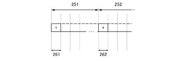
図4では、表示部への書き込み期間と保持期間(1フレーム期間ともいう)の関係につ
いて示している。図4において、期間251、252が保持期間に相当し、期間261、
262が表示部への書き込み期間に相当する。前述の高純度の酸化物半導体層を具備する
トランジスタは、保持期間を長く取ることができるため、特に静止画の表示を行う際に、
画素への書き込み回数を著しく低減することができる。そのため、表示の切り替えが少な
い静止画等の表示では、低消費電力化を図ることができる。
FIG. 4 shows the relationship between the writing period to the display portion and the holding period (also referred to as one frame period). In FIG. 4,
262 corresponds to the writing period to the display portion. Since the above-described transistor including a high-purity oxide semiconductor layer can have a long retention period, particularly when a still image is displayed,
The number of writes to pixels can be significantly reduced. Therefore, low power consumption can be achieved in the case of displaying a still image or the like in which display switching is small.
なお、静止画表示において、保持期間中の駆動用トランジスタのゲートに印加されてい
る電圧の保持率を考慮して、適宜リフレッシュ動作してもよい。例えば、駆動用トランジ
スタのゲートに信号を書き込んだ直後における電圧の値(初期値)に対して所定のレベル
まで電圧が下がったタイミングでリフレッシュ動作を行えばよい。所定のレベルとする電
圧は、初期値に対してチラツキを感じない程度に設定することが好ましい。具体的には、
表示対象が映像の場合、初期値に対して1.0%低い状態、好ましくは0.3%低い状態
となる毎に、リフレッシュ動作(再度の書き込み)を行うのが好ましい。また、表示対象
が文字の場合、初期値に対して10%低い状態、好ましくは3%低い状態となる毎に、リ
フレッシュ動作(再度の書き込み)を行うのが好ましい。
Note that in still image display, a refresh operation may be performed as appropriate in consideration of the retention rate of the voltage applied to the gate of the driving transistor during the retention period. For example, the refresh operation may be performed at the timing when the voltage drops to a predetermined level with respect to the voltage value (initial value) immediately after writing the signal to the gate of the driving transistor. It is preferable to set the voltage at the predetermined level to the extent that flickering does not occur with respect to the initial value. In particular,
When the object to be displayed is an image, it is preferable to perform a refresh operation (write again) each time the initial value is 1.0% lower, preferably 0.3% lower. Further, when the object to be displayed is characters, it is preferable to perform a refresh operation (write again) each time the initial value is reduced by 10%, preferably by 3%.
次に、発光素子6404の駆動方法の一例として、アナログ階調駆動を行う方法を説明
する。第2のトランジスタ6402のゲートに発光素子6404の順方向電圧+第2のト
ランジスタ6402のVth以上の電圧をかける。ここで、発光素子6404の順方向電
圧とは、所望の輝度とする場合の電圧を指し、少なくとも順方向しきい値電圧を含む。例
えば、第2のトランジスタ6402が飽和領域で動作するようなビデオ信号(映像信号)
を入力することで、発光素子6404に電流を流すことができる。なお、第2のトランジ
スタ6402を飽和領域で動作させるためには、電源線6407の電位を第2のトランジ
スタ6402のゲート電位よりも高くするとよい。ビデオ信号をアナログとすることで、
発光素子6404にビデオ信号に応じた電流を流し、アナログ階調駆動を行うことができ
る。
Next, as an example of a method for driving the
By inputting , a current can be supplied to the
Analog gradation driving can be performed by flowing a current corresponding to a video signal to the
また、電圧入力電圧駆動方式によれば、複数の画素を用いた面積階調表示や、発光色が異
なる複数の画素(例えばR、G、B)の組み合わせによる色表現、(例えば、R+G、G
+B、R+B、R+G+B)等が可能である。電圧入力電圧駆動方式の場合には、第2の
トランジスタ6402のゲートには、第2のトランジスタ6402が十分にオンするか、
オフするかの二つの状態となるような信号を入力する。つまり、第2のトランジスタ64
02は線形領域で動作させる。なお、第2のトランジスタ6402を線形領域で動作させ
るためには、電源線6407の電圧を第2のトランジスタ6402のゲート電位よりも低
くするとよい。具体的には、電源線の電位に第2のトランジスタ6402のしきい値電圧
を加えた値以上の電位を与える電圧信号を信号線6405に入力すればよい。
Further, according to the voltage input voltage driving method, area gradation display using a plurality of pixels, color expression by a combination of a plurality of pixels (for example, R, G, B) emitting different colors (for example, R+G, G
+B, R+B, R+G+B), etc. are possible. In the case of the voltage input voltage driving method, the gate of the
A signal is input so as to be in two states of turning off. That is, the second transistor 64
02 operates in the linear region. Note that the voltage of the
なお、発光素子6404をアナログ階調駆動する場合も、電圧入力電圧駆動する場合も、
スイッチング用トランジスタ6401のオフ電流が例えば1×10-16A以下に抑制さ
れているため、第2のトランジスタ6402のゲート電位の保持期間が長い。したがって
、少ない画像信号の書き込み回数でも、表示部での静止画の表示を行うことができる。信
号の書き込みを行う頻度を低減することができるため、低消費電力化を図ることができる
。また、図2に示す画素構成は、これに限定されない。例えば、図2に示す画素に新たに
スイッチ、抵抗素子、容量素子、トランジスタ又は論理回路等を追加してもよい。
In addition, when the
Since the off-state current of the
特に、発光素子の一例として、エレクトロルミネッセンスを利用する発光素子が挙げら
れる。エレクトロルミネッセンスを利用する発光素子は、発光材料が有機化合物であるか
、無機化合物であるかによって区別され、一般的に、前者は有機EL素子、後者は無機E
L素子と呼ばれている。
In particular, as an example of the light-emitting element, there is a light-emitting element utilizing electroluminescence. Light-emitting elements that utilize electroluminescence are classified according to whether the light-emitting material is an organic compound or an inorganic compound. Generally, the former is an organic EL element and the latter is an inorganic E
It is called an L element.
有機EL素子は、一対の電極(陽極及び陰極)と、一対の電極間に設けられた有機化合
物を含む層を有する。陽極の電位を陰極の電位より高くして、有機化合物を含む層に陽極
から正孔を、陰極から電子を注入する。電子および正孔(キャリア)が有機化合物を含む
層にて再結合する際に発光する。
An organic EL element has a pair of electrodes (an anode and a cathode) and a layer containing an organic compound provided between the pair of electrodes. By making the potential of the anode higher than that of the cathode, holes are injected from the anode into the layer containing the organic compound, and electrons are injected from the cathode. Light is emitted when electrons and holes (carriers) recombine in a layer containing an organic compound.
無機EL素子は、その素子構成により、分散型無機EL素子と薄膜型無機EL素子とに
分類される。分散型無機EL素子は、発光材料の粒子をバインダ中に分散させた発光層を
有するものであり、発光メカニズムはドナー準位とアクセプター準位を利用するドナー-
アクセプター再結合型発光である。薄膜型無機EL素子は、発光層を誘電体層で挟み込み
、さらにそれを電極で挟んだ構造であり、発光メカニズムは金属イオンの内殻電子遷移を
利用する局在型発光である。
Inorganic EL elements are classified into dispersion type inorganic EL elements and thin film type inorganic EL elements according to the element structure. A dispersion-type inorganic EL device has a light-emitting layer in which particles of a light-emitting material are dispersed in a binder.
This is acceptor recombination type emission. A thin-film inorganic EL device has a structure in which a light-emitting layer is sandwiched between dielectric layers, which are further sandwiched between electrodes, and the light-emitting mechanism is localized light emission utilizing inner-shell electronic transition of metal ions.
なお、本実施の形態では、発光素子として有機EL素子を用いて説明するが、本発明は
この構成に限定されるものではない。すなわち、本発明は発光素子として無機EL素子を
用いることも可能である。
Note that although an organic EL element is used as a light-emitting element in this embodiment mode, the present invention is not limited to this structure. That is, the present invention can also use an inorganic EL element as a light emitting element.
次に、発光素子を有する表示装置の断面構造について図5を用いて説明する。なお、図
5(A)、図5(B)、図5(C)に例示された駆動用トランジスタ7001、7011
、7021は、高純度の酸化物半導体層を用いたトランジスタとしてもよいし、シリコン
層を用いたトランジスタとしてもよい。本実施の形態においては、駆動用トランジスタ7
001、7011、7021の活性層として高純度の酸化物半導体層を用いた場合につい
て説明する。
Next, a cross-sectional structure of a display device having light-emitting elements will be described with reference to FIG. Note that the driving
, 7021 may be a transistor using a high-purity oxide semiconductor layer or a transistor using a silicon layer. In this embodiment, the driving transistor 7
001, 7011, and 7021 in which a high-purity oxide semiconductor layer is used as an active layer will be described.
本実施の形態で例示する発光素子は、一対の電極(第1の電極及び第2の電極)の間に
EL層(エレクトロルミネッセンス層)が挟まれた構成を有する。第1の電極及び第2の
電極は、一方が陽極として機能し、他方が陰極として機能する。
The light-emitting element described as an example in this embodiment has a structure in which an EL layer (electroluminescent layer) is sandwiched between a pair of electrodes (a first electrode and a second electrode). One of the first electrode and the second electrode functions as an anode and the other functions as a cathode.
陽極として用いる材料は、仕事関数の大きい(具体的には4.0eV以上)金属、合金
、導電性化合物、またはこれらの混合物等が好ましい。具体的には、酸化インジウム-酸
化スズ(ITO:Indium Tin Oxide)、ケイ素若しくは酸化ケイ素を含
有した酸化インジウム-酸化スズ、酸化インジウム-酸化亜鉛(IZO:Indium
Zinc Oxide)、酸化タングステン及び酸化亜鉛を含有した酸化インジウム(I
WZO)等が挙げられる。この他、金(Au)、白金(Pt)、ニッケル(Ni)、タン
グステン(W)、クロム(Cr)、モリブデン(Mo)、鉄(Fe)、コバルト(Co)
、銅(Cu)、パラジウム(Pd)、または金属材料の窒化物(例えば、窒化チタン)等
が挙げられる。
The material used as the anode is preferably a metal, an alloy, a conductive compound, a mixture thereof, or the like having a large work function (specifically, 4.0 eV or more). Specifically, indium oxide-tin oxide (ITO: Indium Tin Oxide), indium oxide containing silicon or silicon oxide-tin oxide, indium oxide-zinc oxide (IZO: Indium
Zinc Oxide), indium oxide containing tungsten oxide and zinc oxide (I
WZO) and the like. In addition, gold (Au), platinum (Pt), nickel (Ni), tungsten (W), chromium (Cr), molybdenum (Mo), iron (Fe), cobalt (Co)
, copper (Cu), palladium (Pd), or nitrides of metal materials (eg, titanium nitride).
陰極として用いる材料は、仕事関数の小さい(具体的には3.8eV以下)金属、合金
、電気伝導性化合物、またはこれらの混合物等が好ましい。具体的には、元素周期表の第
1族または第2族に属する元素、すなわちリチウム(Li)やセシウム(Cs)等のアル
カリ金属、マグネシウム(Mg)、カルシウム(Ca)、ストロンチウム(Sr)等のア
ルカリ土類金属が挙げられる。また、アルカリ金属またはアルカリ土類金属を含む合金(
例えばMgAg、AlLi)を用いることもできる。また、ユウロピウム(Eu)、イッ
テルビウム(Yb)等の希土類金属、または希土類金属を含む合金を用いることもできる
。
また、EL層の一部として、第2の電極に接する電子注入層を設ける場合、仕事関数の大
小に関わらず、Al、Ag、ITO等の様々な導電性材料を第2の電極として用いること
ができる。これら導電性材料は、スパッタリング法やインクジェット法、スピンコート法
等を用いて成膜することが可能である。
The material used as the cathode is preferably a metal, an alloy, an electrically conductive compound, or a mixture thereof with a small work function (specifically, 3.8 eV or less). Specifically, elements belonging to
For example, MgAg, AlLi) can also be used. In addition, rare earth metals such as europium (Eu) and ytterbium (Yb), or alloys containing rare earth metals can also be used.
Further, when providing an electron injection layer in contact with the second electrode as part of the EL layer, various conductive materials such as Al, Ag, and ITO can be used as the second electrode regardless of the magnitude of the work function. can be done. These conductive materials can be deposited using a sputtering method, an inkjet method, a spin coating method, or the like.
EL層は、単層構造で構成されることも可能であるが、通常積層構造から構成される。
EL層の積層構造については特に限定されず、電子輸送性の高い物質を含む層(電子輸送
層)または正孔輸送性の高い物質を含む層(正孔輸送層)、電子注入性の高い物質を含む
層(電子注入層)、正孔注入性の高い物質を含む層(正孔注入層)、バイポーラ性(電子
及び正孔の輸送性の高い物質)の物質を含む層、発光物質を含む層(発光層)等を適宜組
み合わせて構成すればよい。例えば、正孔注入層、正孔輸送層、発光層、電子輸送層、電
子注入層等を適宜組み合わせて構成することができる。また、電荷発生層として機能する
中間層で区切られた複数のEL層を、第1の電極と第2の電極の間に設けた構成であって
もよい。
Although the EL layer can have a single-layer structure, it usually has a laminated structure.
The layered structure of the EL layer is not particularly limited, and a layer containing a substance with high electron transport properties (electron transport layer), a layer containing a substance with high hole transport properties (hole transport layer), or a substance with high electron injection properties. layer (electron injection layer), layer containing a substance with high hole injection property (hole injection layer), layer containing a bipolar substance (substance with high electron and hole transportability), containing a light-emitting substance Layers (light-emitting layers) and the like may be appropriately combined. For example, a hole-injection layer, a hole-transport layer, a light-emitting layer, an electron-transport layer, an electron-injection layer, and the like can be appropriately combined. Alternatively, a structure in which a plurality of EL layers separated by an intermediate layer functioning as a charge generation layer is provided between the first electrode and the second electrode may be employed.
また、発光素子から光を取り出すために、第1の電極又は第2の電極の少なくとも一方
を、透光性を有する導電膜で形成する。基板上に形成された発光素子が発する光を取り出
す方向により発光素子を分類すると、基板の発光素子が形成された側の面から取り出す上
面射出、基板の発光素子が形成された側と反対側の面から取り出す下面射出、基板の発光
素子が形成された側の面及びその反対側の面の双方から取り出す両面射出の3つの代表的
な構造の発光素子がある。本発明は、どの射出構造の発光素子にも適用することができる
。
At least one of the first electrode and the second electrode is formed using a light-transmitting conductive film in order to extract light from the light-emitting element. Light-emitting elements are classified according to the direction in which light emitted from the light-emitting element formed on the substrate is extracted. There are three representative structures of light emitting devices: bottom emission from the surface and dual emission from both the surface of the substrate on which the light emitting elements are formed and the opposite side thereof. The present invention can be applied to light-emitting devices with any emission structure.
また、第1の電極上にEL層を積層する場合、第1の電極の周縁部を隔壁で覆う。隔壁
は、例えばポリイミド、アクリル樹脂、ポリアミド、エポキシ樹脂等の有機樹脂膜、無機
絶縁膜または有機ポリシロキサンを用いて形成すればよいが、例えば感光性の樹脂材料を
用いて隔壁を形成することが好ましい。感光性の樹脂材料を用いた場合は、隔壁の開口部
の側壁が連続した曲率を持った傾斜面となる上、レジストマスクを形成する工程を削減で
きる。
Further, in the case of stacking the EL layer over the first electrode, the peripheral portion of the first electrode is covered with a partition wall. The partition may be formed using, for example, an organic resin film such as polyimide, acrylic resin, polyamide, or epoxy resin, an inorganic insulating film, or organic polysiloxane. For example, the partition can be formed using a photosensitive resin material. preferable. When a photosensitive resin material is used, the side wall of the opening of the partition becomes an inclined surface with a continuous curvature, and the step of forming a resist mask can be eliminated.
なお、基板と発光素子の間にカラーフィルタを形成することもできる。カラーフィルタ
はインクジェット法等の液滴吐出法や、印刷法、フォトリソグラフィ技術を用いたエッチ
ング方法等でそれぞれ形成すればよい。
Note that a color filter can be formed between the substrate and the light emitting element. The color filter may be formed by a droplet discharge method such as an inkjet method, a printing method, an etching method using a photolithography technique, or the like.
また、カラーフィルタ上にオーバーコート層を形成し、さらに保護絶縁層を形成すると
よい。オーバーコート層を設けると、カラーフィルタに起因する凹凸を平坦にできる。保
護絶縁膜を形成すると、不純物がカラーフィルタから発光素子に拡散する現象を防止でき
る。
Further, it is preferable to form an overcoat layer over the color filter and further form a protective insulating layer. By providing the overcoat layer, unevenness caused by the color filter can be flattened. Forming the protective insulating film can prevent a phenomenon in which impurities diffuse from the color filter to the light emitting element.
なお、トランジスタ上の保護絶縁層、オーバーコート層及び絶縁層の上に発光素子を形
成する場合、保護絶縁層、オーバーコート層及び絶縁層を貫通し、トランジスタのソース
電極またはドレイン電極に達するコンタクトホールを形成する。特に、当該コンタクトホ
ールを上述の隔壁と重なる位置にレイアウトして形成すると、開口率の低減を抑制できる
ため好ましい。
Note that when a light-emitting element is formed over a protective insulating layer, an overcoat layer, and an insulating layer over a transistor, a contact hole penetrates through the protective insulating layer, the overcoat layer, and the insulating layer and reaches the source electrode or drain electrode of the transistor. to form In particular, it is preferable to lay out and form the contact hole so as to overlap with the above-described partition wall because reduction in the aperture ratio can be suppressed.
次に、下面射出構造の発光素子を有する画素の構成の一例について説明する。画素に設
けた駆動用トランジスタ7011と、発光素子7012を含む切断面の断面図を図5(A
)に示す。
Next, an example of a structure of a pixel including a light-emitting element with a bottom emission structure will be described. FIG. 5A is a cross-sectional view of a cross-sectional view including a
).
駆動用トランジスタ7011は、基板上に、絶縁層、酸化物半導体層、ソース電極及び
ドレイン電極、ゲート絶縁層、ゲート電極を有し、ソース電極及びドレイン電極にそれぞ
れ配線層が電気的に接続して設けられている。
The driving
また、駆動用トランジスタ7011を覆って絶縁層7031が形成され、絶縁層703
1上に開口部を有するカラーフィルタ7033が設けられている。透光性を有する導電膜
7017は、カラーフィルタ7033を覆って形成されたオーバーコート層7034及び
保護絶縁層7035上に形成されている。なお、駆動用トランジスタ7011のドレイン
電極と導電膜7017は、オーバーコート層7034、保護絶縁層7035、及び絶縁層
7031に形成された開口部を介して電気的に接続している。なお、導電膜7017上に
発光素子7012の第1の電極7013が接して設けられている。
In addition, an insulating
1 is provided with a
発光素子7012は、EL層7014を第1の電極7013と第2の電極7015の間
に挟んで有する。
A light-emitting
透光性を有する導電膜7017としては、酸化タングステンを含むインジウム酸化物、
酸化タングステンを含むインジウム亜鉛酸化物、酸化チタンを含むインジウム酸化物、酸
化チタンを含むインジウム錫酸化物、インジウム錫酸化物(以下、ITOという。)、イ
ンジウム亜鉛酸化物、酸化ケイ素を添加したインジウム錫酸化物等からなる膜を用いるこ
とができる。
As the light-transmitting conductive film 7017, indium oxide containing tungsten oxide,
Indium zinc oxide containing tungsten oxide, indium oxide containing titanium oxide, indium tin oxide containing titanium oxide, indium tin oxide (hereinafter referred to as ITO), indium zinc oxide, indium tin with silicon oxide added A film made of oxide or the like can be used.
ここでは、発光素子7012の第1の電極7013を陰極として用いる場合について説
明する。第1の電極7013を陰極として用いる場合は仕事関数が小さい金属が好適であ
る。図5(A)では、第1の電極7013の膜厚は、光を透過する程度(好ましくは、5
nm~30nm程度)とする。例えば20nmの膜厚を有するアルミニウム膜もしくはM
g-Ag合金膜を第1の電極7013に用いる。
Here, the case where the first electrode 7013 of the
nm to 30 nm). For example, an aluminum film having a thickness of 20 nm or M
A g-Ag alloy film is used for the first electrode 7013 .
なお、透光性を有する導電膜とアルミニウム膜を積層成膜した後、選択的にエッチング
して透光性を有する導電膜7017と第1の電極7013を形成してもよく、この場合、
同じマスクを用いてエッチングすることができ、好ましい。
Note that the light-transmitting conductive film 7017 and the first electrode 7013 may be formed by selectively etching after stacking a light-transmitting conductive film and an aluminum film.
Etching can be performed using the same mask, which is preferable.
また、EL層7014上に形成する第2の電極7015としては、仕事関数が大きい材
料が好ましい。また、第2の電極7015上に遮蔽膜7016、例えば光を遮光する金属
、光を反射する金属等を用いる。本実施の形態では、第2の電極7015としてITO膜
を用い、遮蔽膜7016としてTi膜を用いる。
For the
また、カラーフィルタ7033をオーバーコート層7034で覆い、さらに保護絶縁層
7035で覆う。なお、図5(A)ではオーバーコート層7034は薄い膜厚で図示した
が、オーバーコート層7034は、カラーフィルタ7033に起因する凹凸を平坦化して
いる。
In addition, the
また、オーバーコート層7034及び保護絶縁層7035に形成され、且つ、ドレイン
電極7030に達するコンタクトホールは、隔壁7019と重なる位置に配置されている
。
In addition, a contact hole formed in the
図5(A)に示した画素構造の場合、発光素子7012が発した光は、矢印で示すよう
に第1の電極7013側に射出し、カラーフィルタ7033を透過して表示装置の外にで
る。
In the case of the pixel structure shown in FIG. 5A, light emitted from the
なお、駆動用トランジスタ7011のゲート電極、ソース電極、及びドレイン電極とし
て透光性を有する導電膜を用い、駆動用トランジスタ7011のチャネル形成領域として
、透光性を有する高純度の酸化物半導体層を用いることが好ましい。この場合、図5(A
)に示すように、発光素子7012から発せられる光は、カラーフィルタ7033を通過
して射出されるだけでなく、駆動用トランジスタ7011も通過して射出されることとな
り、開口率を向上させることができる。さらに、駆動用トランジスタ7011のチャネル
形成領域として、透光性を有する高純度の酸化物半導体層を用いることにより、駆動用ト
ランジスタ7011のオフ電流を極めて少なくすることができるため、従来に比較して保
持容量を形成するための電極の面積を縮小することができる。したがって、さらに開口率
を向上させることができる。
Note that a light-transmitting conductive film is used as the gate electrode, the source electrode, and the drain electrode of the driving
), the light emitted from the
次に、両面射出構造の発光素子を有する画素の構成について説明する。画素に設けた駆
動用トランジスタ7021と、発光素子7022を含む切断面の断面図を図5(B)に示
す。
Next, the configuration of a pixel having a light emitting element with a dual emission structure will be described. A cross-sectional view including a
駆動用トランジスタ7021は、基板上に、絶縁層、酸化物半導体層、ソース電極及び
ドレイン電極、ゲート絶縁層、ゲート電極を有し、ソース電極及びドレイン電極にそれぞ
れ配線層が電気的に接続して設けられている。
The driving
また、駆動用トランジスタ7021を覆って絶縁層7041が形成され、絶縁層704
1上に開口部を有するカラーフィルタ7043が設けられている。透光性を有する導電膜
7027は、カラーフィルタ7043を覆って形成されたオーバーコート層7044及び
絶縁層7045上に形成されている。なお、駆動用トランジスタ7021のドレイン電極
と導電膜7027は、オーバーコート層7044、絶縁層7045、及び絶縁層7041
に形成された開口部を介して電気的に接続している。なお、導電膜7027上に発光素子
7022の第1の電極7023が接して設けられている。
In addition, an insulating
1 is provided with a
are electrically connected through an opening formed in the Note that the
発光素子7022は、EL層7024を第1の電極7023と第2の電極7025の間
に挟んで有する。
A light-emitting
ここでは、発光素子7022の第1の電極7023を陰極として用いる場合について説
明する。なお、透光性を有する導電膜7027は図5(A)に示す導電膜7017と同様
に形成すればよく、また、第1の電極7023は図5(A)に示す第1の電極7013と
同様に形成すればよく、また、EL層7024は図5(A)に示すEL層7014と同様
に形成すればよいため、ここでは詳細な説明を割愛する。
Here, the case where the
EL層7024上に形成する第2の電極7025は、ここでは陽極として機能するため
、仕事関数が大きい材料、例えば、ITO、IZO、ZnO等の透明導電性材料が好まし
い。本実施の形態では、第2の電極7025としてITOを形成する。
Since the
また、カラーフィルタ7043、オーバーコート層7044及び保護絶縁層7045は
、図5(A)で例示した画素が有するカラーフィルタ7033、オーバーコート層703
4及び保護絶縁層7035とそれぞれ同様に形成すればよい。
Further, the
4 and the protective insulating
図5(B)に示した素子構造の場合、発光素子7022から発せられる光は、矢印で示
すように第1の電極7023側と第2の電極7025側の両方に射出し、第1の電極70
23側の光はカラーフィルタ7043を透過して表示装置の外にでる。
In the element structure shown in FIG. 5B, light emitted from the light-emitting
The light on the 23 side passes through the
なお、図5(B)ではゲート電極、ソース電極、及びドレイン電極として透光性を有す
る導電膜を用いて駆動用トランジスタ7021を構成する例を示している。従って、発光
素子7022から発せられる光の一部は、カラーフィルタ7043と駆動用トランジスタ
7021を通過して射出する。
Note that FIG. 5B shows an example in which the
また、オーバーコート層7044及び保護絶縁層7045に形成され、且つ、ドレイン
電極7040に達するコンタクトホールは、隔壁7029と重なる位置に配置されている
。ドレイン電極に達するコンタクトホールと、隔壁7029とを重ねるレイアウトとする
ことで第2の電極7025側の開口率と第1の電極7023側の開口率をほぼ同一とする
ことができる。
A contact hole formed in the
ただし、両面射出構造の発光素子のどちらの表示面もフルカラー表示とする場合、第2
の電極7025側からの光はカラーフィルタ7043を通過しないため、別途カラーフィ
ルタを備えた封止基板を第2の電極7025上方に設けることが好ましい。
However, when both display surfaces of the light emitting element of the double emission structure are used for full color display, the second
Since the light from the
次に、上面射出構造の発光素子を有する画素の構成について説明する。画素に設けた駆
動用トランジスタ7001と、発光素子7002を含む切断面の断面図を図5(C)に示
す。
Next, the structure of a pixel having a light emitting element with a top emission structure will be described. FIG. 5C shows a cross-sectional view including a
駆動用トランジスタ7001は、基板上に、絶縁層、酸化物半導体層、ソース電極及び
ドレイン電極、ゲート絶縁層、ゲート電極を有し、ソース電極及びドレイン電極にそれぞ
れ配線層が電気的に接続して設けられている。
The driving
また、駆動用トランジスタ7001を覆って絶縁層7051が形成され、絶縁層705
1上に開口部を有する絶縁層7053が設けられている。第1の電極7003は、絶縁層
7053を覆って形成された絶縁層7055上に形成されている。なお、駆動用トランジ
スタ7001のドレイン電極と第1の電極7003は、絶縁層7055、及び絶縁層70
51に形成された開口部を介して電気的に接続している。
An insulating
1, an insulating
It is electrically connected through an opening formed in 51 .
なお、絶縁層7053は、ポリイミド、アクリル樹脂、ベンゾシクロブテン樹脂、ポリ
アミド、エポキシ等の樹脂材料を用いることができる。また上記樹脂材料の他に、低誘電
率材料(low-k材料)、シロキサン系樹脂、PSG(リンガラス)、BPSG(リン
ボロンガラス)等を用いることができる。なお、これらの材料で形成される絶縁膜を複数
積層させることで、絶縁層7053を形成してもよい。絶縁層7053の形成法は、特に
限定されず、その材料に応じて、スパッタ法、SOG法、スピンコート、ディップ、スプ
レー塗布、液滴吐出法(インクジェット法、スクリーン印刷、オフセット印刷等)、ドク
ターナイフ、ロールコーター、カーテンコーター、ナイフコーター等を用いることができ
る。絶縁層7053を形成することで、例えば駆動用トランジスタに起因する凹凸を平坦
にできる。また、絶縁層7055及び絶縁層7053に形成され、且つ、ドレイン電極7
050に達するコンタクトホールは、隔壁7009と重なる位置に配置されている。
Note that for the insulating
A contact hole reaching 050 is arranged at a position overlapping with the
発光素子7002は、EL層7004を第1の電極7003と第2の電極7005の間
に挟んで有する。図5(C)に例示する発光素子7002においては、第1の電極700
3を陰極として用いる場合について説明する。
A light-emitting
3 is used as a cathode.
第1の電極7003は図5(A)に示す第1の電極7013と同様の材料を適用すれば
よいが、図5(C)に示す上面射出構造の発光素子においては、第1の電極7003は透
光性を有さず、むしろ高い反射率を有する電極であることが好ましい。高い反射率を有す
る電極を用いることで、発光の取り出し効率を高めることができる。
A material similar to that of the first electrode 7013 shown in FIG. 5A may be used for the
第1の電極7003としては、例えばアルミニウム膜もしくはアルミニウムを主成分と
する合金膜、またはアルミニウム膜にチタン膜を積層したものが好ましい。図5(C)で
は、Ti膜、アルミニウム膜、Ti膜の順に積層した積層膜を第1の電極7003に用い
る。
As the
また、EL層7004は図5(A)に示すEL層7014と同様に形成すればよく、ま
た、第2の電極7005は図5(B)に示す第2の電極7025と同様に形成すればよい
ため、ここでは詳細な説明を割愛する。
Further, the
図5(C)に示した素子構造の場合、発光素子7002から発せられる光は、矢印で示
すように第2の電極7005側に射出する。
In the element structure shown in FIG. 5C, light emitted from the
図5(C)の構造を用いてフルカラー表示を行う場合、例えば発光素子7002を緑色
発光素子とし、隣り合う一方の発光素子を赤色発光素子とし、もう一方の発光素子を青色
発光素子とする。また、3種類の発光素子だけでなく白色素子を加えた4種類の発光素子
でフルカラー表示ができる発光表示装置を作製してもよい。
When full color display is performed using the structure of FIG. 5C, for example, the
また、図5(C)の構造に配置する複数の発光素子を全て白色発光素子として、発光素
子7002を含むそれぞれの発光素子の上方にカラーフィルタ等を有する封止基板を配置
する構成とし、フルカラー表示ができる発光表示装置を作製してもよい。白色等の単色の
発光を示す材料を形成し、カラーフィルタや色変換層を組み合わせることによりフルカラ
ー表示を行うことができる。
Further, all the plurality of light-emitting elements arranged in the structure in FIG. 5C are white light-emitting elements, and a sealing substrate having a color filter or the like is arranged above each light-emitting element including the light-emitting
また、必要に応じて、円偏光板等の光学フィルムを設けてもよい。 Moreover, you may provide optical films, such as a circularly-polarizing plate, as needed.
次に、表示装置の一形態に相当する発光表示パネル(発光パネルともいう)の外観及び
断面について、図6を用いて説明する。図6(A)は、第1の基板上に形成されたトラン
ジスタ及び発光素子を、第2の基板との間にシール材によって封止した、パネルの平面図
であり、図6(B)は、図6(A)のH-Iにおける断面図に相当する。
Next, the appearance and cross section of a light-emitting display panel (also referred to as a light-emitting panel), which is one mode of a display device, will be described with reference to FIGS. FIG. 6A is a plan view of a panel in which a transistor and a light-emitting element formed over a first substrate are sealed between them and a second substrate with a sealing material, and FIG. , corresponds to a cross-sectional view taken along line HI of FIG. 6(A).
第1の基板4501上に設けられた画素部4502、信号線駆動回路4503a、45
03b、及び走査線駆動回路4504a、4504bを囲むようにして、シール材450
5が設けられている。また画素部4502、信号線駆動回路4503a、4503b、及
び走査線駆動回路4504a、4504bの上に第2の基板4506が設けられている。
よって画素部4502、信号線駆動回路4503a、4503b、及び走査線駆動回路4
504a、4504bは、第1の基板4501とシール材4505と第2の基板4506
とによって、充填材4507と共に密封されている。このように画素部4502、信号線
駆動回路4503a、4503b、及び走査線駆動回路4504a、4504bが外気に
曝されないように気密性が高く、脱ガスの少ない保護フィルム(貼り合わせフィルム、紫
外線硬化樹脂フィルム等)やカバー材でパッケージング(封入)することが好ましい。
A
03b, and scanning
5 is provided. A
Therefore, the
504a and 4504b are the
It is sealed together with the
また、第1の基板4501上に設けられた画素部4502、信号線駆動回路4503a
、4503b、及び走査線駆動回路4504a、4504bは、トランジスタを複数有し
ており、図6(B)では、画素部4502に含まれるトランジスタ4510と、信号線駆
動回路4503aに含まれるトランジスタ4509とを例示している。トランジスタ45
09、4510上には絶縁層4542-4545が設けられている。また、絶縁層454
2-4545に設けられたコンタクトホールを介して、トランジスタ4510のソース電
極またはドレイン電極4848と発光素子4511の第1の電極層4517が電気的に接
続されている。
A
, 4503b, and scan
09, 4510 are provided with insulating layers 4542-4545. Also, the insulating layer 454
A source or drain electrode 4848 of the
本実施の形態においては、信号線駆動回路4503aに含まれるトランジスタ4509
、及び画素部4502に含まれるトランジスタ4510として、高純度の酸化物半導体層
を有するトランジスタをそれぞれ用いる。
In this embodiment mode, the
, and the
絶縁層4542上において、駆動回路用のトランジスタ4509の酸化物半導体層のチ
ャネル形成領域と重なる位置に導電層4540が設けられている。導電層4540を酸化
物半導体層のチャネル形成領域と重なる位置に設けることによって、BTストレス試験(
バイアス・温度ストレス試験)前後におけるトランジスタ4509のしきい値電圧の変化
量を低減することができる。なお、本明細書中で、BTストレス試験(バイアス・温度ス
トレス試験)とは、トランジスタに高温雰囲気下で、高ゲート電圧を印加する試験のこと
を指す。また、導電層4540は、電位がトランジスタ4509のゲート電極と同じでも
よいし、異なっていても良く、第2のゲート電極として機能させることもできる。また、
導電層4540の電位がGND、0V、またはフローティング状態であってもよい。
A
The amount of change in the threshold voltage of the
The potential of the
発光素子4511の構成は、第1の電極層4517、電界発光層4512、第2の電極
層4513の積層構造であるが、ここに示す構成に限定されない。発光素子4511から
取り出す光の方向等に合わせて、発光素子4511の構成は適宜変えることができる。
The structure of the light-emitting
隔壁4520は、有機樹脂膜、無機絶縁膜または有機ポリシロキサンを用いて形成する
。特に感光性の材料を用い、隔壁4520の側壁が連続した曲率を持って形成される傾斜
面となるように形成することが好ましい。
The
電界発光層4512は、単数の層で構成されていても、複数の層が積層されるように構
成されていてもどちらでもよい。
The
発光素子4511に酸素、水素、水分、二酸化炭素等が侵入しないように、第2の電極
層4513及び隔壁4520上に保護膜を形成してもよい。保護膜としては、窒化珪素膜
、窒化酸化珪素膜、DLC膜等を形成することができる。
A protective film may be formed over the
また、信号線駆動回路4503a、4503b、走査線駆動回路4504a、4504
b、または画素部4502に与えられる各種信号及び電位は、FPC4518a、451
8bから供給されている。
Signal
b, or various signals and potentials applied to the
8b.
接続端子電極4515は、発光素子4511が有する第1の電極層4517と同じ導電
膜から形成されている。また、端子電極4516は、トランジスタ4509、4510が
有するソース電極及びドレイン電極と同じ導電膜から形成されている。
The
接続端子電極4515は、FPC4518aが有する端子と、異方性導電膜4519を
介して電気的に接続されている。
The
発光素子4511からの光の取り出し方向に位置する基板は透光性でなければならない
。その場合には、ガラス板、プラスチック板、ポリエステルフィルムまたはアクリルフィ
ルムのような透光性を有する材料を用いる。
A substrate positioned in a direction in which light is extracted from the
また、充填材4507としては窒素やアルゴン等の不活性な気体の他に、紫外線硬化樹
脂または熱硬化樹脂を用いることができ、PVC(ポリビニルクロライド)、アクリル、
ポリイミド、エポキシ樹脂、シリコーン樹脂、PVB(ポリビニルブチラル)またはEV
A(エチレンビニルアセテート)を用いることができる。例えば充填材として窒素を用い
ればよい。
As the
Polyimide, epoxy resin, silicone resin, PVB (polyvinyl butyral) or EV
A (ethylene vinyl acetate) can be used. For example, nitrogen may be used as the filler.
また、必要に応じて、発光素子の射出面に偏光板、又は円偏光板(楕円偏光板を含む)
、位相差板(λ/4板、λ/2板)、カラーフィルタ等の光学フィルムを適宜設けてもよ
い。また、偏光板又は円偏光板に反射防止膜を設けてもよい。例えば、表面の凹凸により
反射光を拡散し、映り込みを低減できるアンチグレア処理を施すことができる。
In addition, if necessary, a polarizing plate or a circularly polarizing plate (including an elliptically polarizing plate) is placed on the exit surface of the light-emitting element.
, a retardation plate (λ/4 plate, λ/2 plate), and an optical film such as a color filter may be provided as appropriate. Also, an antireflection film may be provided on the polarizing plate or the circularly polarizing plate. For example, anti-glare treatment can be applied to diffuse reflected light by unevenness of the surface and reduce glare.
なお、本発明は、図6の構成に限定されない。すなわち、信号線駆動回路4503a、
4503b、及び走査線駆動回路4504a、4504bは、別途用意された基板上に単
結晶半導体膜又は多結晶半導体膜によって形成された駆動回路で実装されていてもよい。
また、信号線駆動回路のみ、或いは一部、又は走査線駆動回路のみ、或いは一部のみを別
途形成して実装されていてもよい。
Note that the present invention is not limited to the configuration of FIG. That is, the signal
The 4503b and the scanning
Alternatively, only or part of the signal line driver circuit, or only or part of the scanning line driver circuit may be separately formed and mounted.
(実施の形態2)
本実施の形態では、表示装置の消費電力を更に抑制する構成について説明する。具体的
には、表示装置の画素部における消費電力を抑制することに加え、表示装置の駆動回路部
における消費電力を抑制する構成について説明する。
(Embodiment 2)
In this embodiment mode, a structure for further reducing power consumption of a display device will be described. Specifically, a structure for suppressing power consumption in a driver circuit portion of a display device in addition to suppressing power consumption in a pixel portion of the display device will be described.
図7は、表示装置のブロック図の一例を示すものである。ただし、本発明は図7の構成
に限定されるものではない。
FIG. 7 shows an example of a block diagram of a display device. However, the present invention is not limited to the configuration of FIG.
図7に示す表示装置1000は、表示パネル1001、信号生成回路1002、記憶回
路1003、比較回路1004、選択回路1005、表示制御回路1006を有する。ま
た、表示パネル1001は、駆動回路部1007、画素部1008を有する。また、駆動
回路部1007は、ゲート線駆動回路1009A、信号線駆動回路1009Bを有する。
また、ゲート線駆動回路1009A、信号線駆動回路1009Bは、複数の画素を有する
画素部1008を駆動する機能を有する。
A
Further, the gate
画素部1008を構成するトランジスタには、実施の形態1で説明したものを用いる。
すなわち、スイッチング用トランジスタとして、高純度の酸化物半導体層を有するnチャ
ネル型のトランジスタを用いる。なお、駆動用トランジスタは、高純度の酸化物半導体層
を用いた構成としてもよいし、シリコン層を用いた構成としてもよいが、本実施の形態に
おいては、駆動用トランジスタにも高純度の酸化物半導体層を有するnチャネル型のトラ
ンジスタを適用する場合について説明する。
As the transistor forming the
That is, an n-channel transistor including a highly purified oxide semiconductor layer is used as a switching transistor. Note that the driving transistor may have a structure using a high-purity oxide semiconductor layer or a structure using a silicon layer. A case of applying an n-channel transistor having a semiconductor layer will be described.
本実施の形態においては、画素部1008を構成するトランジスタの一つであるスイッ
チング用トランジスタとして、高純度の酸化物半導体層を有するnチャネル型のトランジ
スタを用いることにより、画像信号等のデータの保持時間を長く取ることができる。この
ため、静止画等の表示を行う際に、信号の書き込みを行う頻度を低減できる。したがって
、表示装置の低消費電力化を図ることができる。
In this embodiment, an n-channel transistor including a high-purity oxide semiconductor layer is used as a switching transistor which is one of transistors included in the
さらに、本実施の形態においては、静止画表示を行う際に、画素部に含まれる全ての信
号線及び/または全ての走査線に供給される信号の出力を停止するように駆動回路部を動
作させることにより、画素部だけでなく駆動回路部の消費電力も抑制することができる。
すなわち、表示装置が静止画像を表示する期間の間に、前記画素部に含まれる全ての信号
線及び/または全ての走査線に供給される信号の出力が停止される期間を有する。本実施
の形態においては、駆動回路部の低消費電力化を実現するための一構成として、表示装置
1000が信号生成回路1002、記憶回路1003、比較回路1004、選択回路10
05、表示制御回路1006を有する。
Further, in this embodiment mode, when displaying a still image, the driver circuit portion is operated so as to stop outputting signals supplied to all signal lines and/or all scanning lines included in the pixel portion. Thus, power consumption of not only the pixel portion but also the driver circuit portion can be suppressed.
That is, a period during which the display device displays a still image includes a period during which output of signals supplied to all signal lines and/or all scanning lines included in the pixel portion is stopped. In this embodiment mode, the
05, it has a
信号生成回路1002は、ゲート線駆動回路1009A、及び信号線駆動回路1009
Bを駆動するために必要な信号(制御信号)を生成する機能を有する。そして、信号生成
回路1002は、配線を介して制御信号を駆動回路部1007に出力するとともに、配線
を介して画像信号(ビデオ電圧、ビデオ信号、ビデオデータともいう)を記憶回路100
3に出力する機能を有する。換言すれば、信号生成回路1002は、駆動回路部1007
を駆動するための制御信号、及び画素部に供給する画像信号を生成し出力するための回路
である。
The
It has a function of generating a signal (control signal) necessary for driving B. The
It has a function to output to 3. In other words, the
and a circuit for generating and outputting an image signal to be supplied to the pixel portion.
具体的には、信号生成回路1002は、制御信号として、ゲート線駆動回路1009A
、及び信号線駆動回路1009Bに電源電圧である高電源電位Vdd、低電源電位Vss
を供給し、ゲート線駆動回路1009Aには、ゲート線駆動回路用のスタートパルスSP
、クロック信号CKを供給し、信号線駆動回路1009Bには、信号線駆動回路用のスタ
ートパルスSP、クロック信号CKを供給する。また信号生成回路1002は、動画像ま
たは静止画を表示するための画像信号Dataを記憶回路1003に出力する。
Specifically, the
, and a high power supply potential Vdd and a low power supply potential Vss which are power supply voltages to the signal
is supplied to the gate
, supplies a clock signal CK, and supplies a start pulse SP for the signal line driver circuit and a clock signal CK to the signal
なお、動画像は、複数のフレームに時分割した複数の画像を高速に切り替えることで人
間の目に動画像として認識される画像のことをいう。具体的には、1秒間に60回(60
フレーム)以上画像を切り替えることで、人間の目にはちらつきが少なく動画像と認識さ
れる、連続する画像信号のことである。一方静止画は、動画像と異なり、複数のフレーム
期間に時分割した複数の画像を高速に切り替えて動作させるものの、連続するフレーム期
間、例えばnフレーム目と、(n+1)フレーム目とで画像信号が変化しない画像信号の
ことをいう。
Note that a moving image is an image recognized as a moving image by human eyes by switching at high speed a plurality of images time-divided into a plurality of frames. Specifically, 60 times per second (60
It is a continuous image signal that is recognized as a moving image with little flicker by the human eye by switching images over a frame). On the other hand, unlike a moving image, a still image is operated by switching a plurality of images time-divided into a plurality of frame periods at high speed. is an image signal that does not change.
なお、信号生成回路1002は、他にも画像信号、ラッチ信号等を生成する機能を有し
ていてもよい。また、信号生成回路1002は、ゲート線駆動回路1009A及び/また
は信号線駆動回路1009Bに対し、各駆動回路のパルス信号の出力を停止するためのリ
セット信号Res信号を出力する機能を有していてもよい。また、各信号は第1のクロッ
ク信号、第2のクロック信号といったように複数の信号で構成される信号であってもよい
。
Note that the
なお、高電源電位Vddとは、基準電位より高い電位のことであり、低電源電位とは基
準電位以下の電位のことをいう。なお高電源電位及び低電源電位ともに、トランジスタが
動作できる程度の電位であることが望ましい。
Note that the high power supply potential Vdd is higher than the reference potential, and the low power supply potential is lower than the reference potential. Note that both the high power supply potential and the low power supply potential are preferably potentials at which the transistor can operate.
なお、電圧とは、ある電位と、基準の電位(例えばグラウンド電位)との電位差のこと
を示す場合が多い。よって、電圧、電位、電位差を、各々、電位、電圧、電圧と言い換え
ることが可能である。
Note that voltage often indicates a potential difference between a certain potential and a reference potential (for example, ground potential). Therefore, voltage, potential, and potential difference can be replaced with potential, voltage, and voltage, respectively.
また、信号生成回路1002から記憶回路1003への画像信号の出力がアナログの信
号の場合には、A/Dコンバータ等を介してデジタルの信号に変換して、記憶回路100
3に出力する構成とすればよい。
Further, when the image signal output from the
3 may be used.
記憶回路1003は、複数のフレームに関する画像信号を記憶するための複数のフレー
ムメモリ1010を有する。なおフレームメモリは、例えばDRAM(Dynamic
Random Access Memory)、SRAM(Static Random
Access Memory)等の記憶素子を用いて構成すればよい。
The
Random Access Memory), SRAM (Static Random
A storage element such as an access memory may be used.
なお、フレームメモリ1010は、フレーム期間毎に画像信号を記憶する構成であれば
よく、フレームメモリの数について特に限定されるものではない。またフレームメモリ1
010の画像信号は、比較回路1004及び選択回路1005により選択的に読み出され
るものである。
Note that the number of
The 010 image signal is selectively read out by the
比較回路1004は、記憶回路1003に記憶された連続するフレーム期間の画像信号
を選択的に読み出して、当該画像信号の比較を行い、差分を検出するための回路である。
当該比較回路1004での画像信号の比較により差分が検出された場合、当該差分が検出
された連続するフレーム期間では動画像であると判断される。一方、比較回路1004で
の画像信号の比較により差分が検出されなかった場合、当該差分が検出されなかった連続
するフレーム期間では静止画であると判断される。すなわち、比較回路1004での差分
の検出によって、連続するフレーム期間の画像信号が、動画像を表示するための画像信号
であるか、または静止画を表示するための画像信号であるか、の判断がなされるものであ
る。なお、当該比較により得られる差分の検出は、一定のレベルを超えたときに差分を検
出したと判断されるように設定してもよい。
The
When a difference is detected by comparison of image signals in the
選択回路1005は、複数のスイッチ、例えばトランジスタで形成されるスイッチを設
け、動画像を表示するための画像信号が比較回路での差分の検出により判断された際に、
当該画像信号が記憶されたフレームメモリ1010より画像信号を選択して表示制御回路
1006に出力するための回路である。なお比較回路1004で比較したフレーム間の画
像信号の差分が検出されなければ、連続するフレーム間で表示される画像は静止画であり
、この場合、連続するフレーム期間のうち、後者の画像信号について表示制御回路100
6に出力しない構成とすればよい。
The
This is a circuit for selecting an image signal from the
6 is not output.
表示制御回路1006は、画像信号、高電源電位Vdd、低電源電位Vss、スタート
パルスSP、クロック信号CK、及びリセット信号Resの制御信号に関して、駆動回路
部1007への供給または停止を切り替える為の回路である。具体的には、比較回路10
04により動画像と判断、すなわち連続フレーム期間の画像信号の差分が抽出された場合
には、画像信号が選択回路1005より表示制御回路1006に供給される。そして、表
示制御回路1006を介して駆動回路部1007に画像信号が供給される。また、制御信
号が表示制御回路1006を介して駆動回路部1007に供給されることとなる。一方、
比較回路1004により静止画と判断、すなわち連続フレーム期間の画像信号の差分を抽
出しない場合には、画像信号が選択回路1005より供給されないため、表示制御回路1
006より駆動回路部1007に画像信号が供給されない。また、制御信号の駆動回路部
1007への供給を表示制御回路1006が停止することとなる。
The
04 determines that the image is a moving image, that is, when the difference between the image signals in the continuous frame period is extracted, the image signal is supplied from the
When the
006 does not supply an image signal to the
なお、静止画と判断される場合において、静止画と判断される期間が短い場合には、制
御信号のうち、高電源電位Vdd、低電源電位Vssの停止を行わない構成としてもよい
。この場合、頻繁に高電源電位Vdd、低電源電位Vssの停止及び再開を行うことによ
る消費電力の増大を低減することができるため、好ましい。
Note that when the image is determined to be a still image, if the period during which the image is determined to be a still image is short, the high power supply potential Vdd and the low power supply potential Vss of the control signals may not be stopped. This is preferable because an increase in power consumption due to frequent stopping and restarting of the high power supply potential Vdd and the low power supply potential Vss can be reduced.
なお、画像信号及び制御信号の停止は、画素部1008の各画素で画像信号を保持でき
る期間にわたって行うことが望ましく、各画素での保持期間の後に再度画像信号を供給す
るよう、表示制御回路1006が先に供給した画像信号及び制御信号を再度供給するよう
にする構成とすればよい。
Note that the image signal and the control signal are preferably stopped for a period in which each pixel in the
なお、信号の供給とは、配線に所定の電位を供給することをいう。また、信号の停止と
は、配線への所定の電位の供給を停止し、所定の固定電位が供給される配線、例えば低電
源電位Vssが供給された配線に電気的に接続することをいう。または、信号の停止とは
、所定の電位が供給されている配線との電気的な接続を切断し、浮遊状態とすることをい
う。
Note that supplying a signal means supplying a predetermined potential to a wiring. Stopping a signal means stopping supply of a predetermined potential to a wiring and electrically connecting to a wiring supplied with a predetermined fixed potential, for example, a wiring supplied with a low power supply potential Vss. Alternatively, stopping a signal means cutting off an electrical connection with a wiring to which a predetermined potential is supplied to bring the element into a floating state.
上述のように映像信号を比較して動画像か静止画かを判定し、クロック信号やスタート
パルス等の制御信号の駆動回路部への供給の再開または停止を選択的に行うことで、駆動
回路部1007における消費電力を抑制することができる。
As described above, the video signal is compared to determine whether it is a moving image or a still image. Power consumption in the
次に、駆動回路部1007のゲート線駆動回路1009A、信号線駆動回路1009B
を構成するシフトレジスタの構成について図8に一例を示す。
Next, a gate
FIG. 8 shows an example of the configuration of the shift register that constitutes the .
図8(A)に示すシフトレジスタは、第1のパルス出力回路10_1乃至第Nのパルス
出力回路10_N(Nは3以上の自然数)を有している。図8(A)に示すシフトレジス
タの第1のパルス出力回路10_1乃至第Nのパルス出力回路10_Nには、第1の配線
11より第1のクロック信号CK1、第2の配線12より第2のクロック信号CK2、第
3の配線13より第3のクロック信号CK3、第4の配線14より第4のクロック信号C
K4が供給される。また第1のパルス出力回路10_1では、第5の配線15からのスタ
ートパルスSP1(第1のスタートパルス)が入力される。また2段目以降の第nのパル
ス出力回路10_n(nは、2以上N以下の自然数)では、一段前段のパルス出力回路か
らの信号(前段信号OUT(n-1)(SR)という)が入力される。また第1のパルス
出力回路10_1では、2段後段の第3のパルス出力回路10_3からの信号が入力され
る。同様に、2段目以降の第nのパルス出力回路10_nでは、2段後段の第(n+2)
のパルス出力回路10_(n+2)からの信号(後段信号OUT(n+2)(SR)とい
う)が入力される。従って、各段のパルス出力回路からは、後段及び/または二つ前の段
のパルス出力回路に入力するための第1の出力信号(OUT(1)(SR)~OUT(N
)(SR))、別の配線等に入力される第2の出力信号(OUT(1)~OUT(N))
が出力される。なお、図8(A)に示すように、シフトレジスタの最終段の2つの段には
、後段信号OUT(n+2)(SR)が入力されないため、一例としては、別途第6の配
線17より第2のスタートパルスSP2、第7の配線18より第3のスタートパルスSP
3をそれぞれ入力する構成でもよい。または、別途シフトレジスタの内部で生成された信
号であってもよい。例えば、画素部へのパルス出力に寄与しない第(N+1)のパルス出
力回路10_(N+1)、第(N+2)のパルス出力回路10_(N+2)を設け(ダミ
ー段ともいう)、当該ダミー段より第2のスタートパルス(SP2)及び第3のスタート
パルス(SP3)に相当する信号を生成する構成としてもよい。
The shift register illustrated in FIG. 8A includes a first pulse output circuit 10_1 to an Nth pulse output circuit 10_N (N is a natural number of 3 or more). The first pulse output circuit 10_1 to the Nth pulse output circuit 10_N of the shift register shown in FIG. Clock signal CK2, third clock signal CK3 from
K4 is supplied. A start pulse SP1 (first start pulse) from the
A signal (referred to as a post-stage signal OUT(n+2)(SR)) from the pulse output circuit 10_(n+2) is input. Therefore, from the pulse output circuit of each stage, the first output signals (OUT(1)(SR) to OUT(N
) (SR)), second output signals (OUT(1) to OUT(N)) input to separate wirings, etc.
is output. As shown in FIG. 8A, since the latter stage signal OUT(n+2) (SR) is not input to the last two stages of the shift register, as an example, the
3 may be input. Alternatively, it may be a signal generated inside the shift register separately. For example, the (N+1)th pulse output circuit 10_(N+1) and the (N+2)th pulse output circuit 10_(N+2) that do not contribute to the pulse output to the pixel portion are provided (also referred to as a dummy stage), and the 2 start pulse (SP2) and a third start pulse (SP3).
第1のクロック信号(CK1)乃至第4のクロック信号(CK4)は、図9に示すよう
に、一定の間隔でH信号とL信号を繰り返す信号である。また、第1のクロック信号(C
K1)乃至第4のクロック信号(CK4)は、順に1/4周期分遅延している。本実施の
形態では、第1のクロック信号(CK1)乃至第4のクロック信号(CK4)を利用して
、パルス出力回路の駆動の制御等を行う。なお、クロック信号CKは、入力される駆動回
路に応じて、GCK、SCKということもあるが、ここではCKとして説明を行う。
The first clock signal (CK1) to the fourth clock signal (CK4) are signals that repeat H signal and L signal at regular intervals, as shown in FIG. Also, the first clock signal (C
K1) to the fourth clock signal (CK4) are delayed by 1/4 period in order. In this embodiment mode, driving control of the pulse output circuit and the like are performed using the first clock signal (CK1) to the fourth clock signal (CK4). Note that the clock signal CK may be GCK or SCK depending on the drive circuit to which it is input, but here it will be explained as CK.
第1のパルス出力回路10_1乃至第Nのパルス出力回路10_Nの各々は、第1の入
力端子21、第2の入力端子22、第3の入力端子23、第4の入力端子24、第5の入
力端子25、第1の出力端子26、第2の出力端子27を有している(図8(B)参照)
。
Each of the first pulse output circuit 10_1 to the Nth pulse output circuit 10_N has a
.
第1の入力端子21、第2の入力端子22及び第3の入力端子23は、第1の配線11
~第4の配線14のいずれかと電気的に接続されている。例えば、図8(A)、(B)に
おいて、第1のパルス出力回路10_1は、第1の入力端子21が第1の配線11と電気
的に接続され、第2の入力端子22が第2の配線12と電気的に接続され、第3の入力端
子23が第3の配線13と電気的に接続されている。また、第2のパルス出力回路10_
2は、第1の入力端子21が第2の配線12と電気的に接続され、第2の入力端子22が
第3の配線13と電気的に接続され、第3の入力端子23が第4の配線14と電気的に接
続されている。
The
to any of the
2, the
また図8(A)、(B)において、第1のパルス出力回路10_1は、第4の入力端子
24にスタートパルスが入力され、第5の入力端子25に後段信号OUT(3)(SR)
が入力され、第1の出力端子26より第1の出力信号OUT(1)(SR)が出力され、
第2の出力端子27より第2の出力信号OUT(1)が出力されていることとなる。
8A and 8B, the first pulse output circuit 10_1 has a
is input, a first output signal OUT (1) (SR) is output from the
A second output signal OUT(1) is output from the
次に、パルス出力回路の具体的な回路構成の一例について、図8(C)で説明する。 Next, an example of a specific circuit configuration of the pulse output circuit will be described with reference to FIG.
図8(C)において第1のトランジスタ31は、第1端子が電源線51に電気的に接続
され、第2端子が第9のトランジスタ39の第1端子に電気的に接続され、ゲートが第4
の入力端子24に電気的に接続されている。第2のトランジスタ32は、第1端子が電源
線52に電気的に接続され、第2端子が第9のトランジスタ39の第1端子に電気的に接
続され、ゲートが第4のトランジスタ34のゲートに電気的に接続されている。第3のト
ランジスタ33は、第1端子が第1の入力端子21に電気的に接続され、第2端子が第1
の出力端子26に電気的に接続されている。第4のトランジスタ34は、第1端子が電源
線52に電気的に接続され、第2端子が第1の出力端子26に電気的に接続されている。
第5のトランジスタ35は、第1端子が電源線52に電気的に接続され、第2端子が第2
のトランジスタ32のゲート及び第4のトランジスタ34のゲートに電気的に接続され、
ゲートが第4の入力端子24に電気的に接続されている。第6のトランジスタ36は、第
1端子が電源線51に電気的に接続され、第2端子が第2のトランジスタ32のゲート及
び第4のトランジスタ34のゲートに電気的に接続され、ゲートが第5の入力端子25に
電気的に接続されている。第7のトランジスタ37は、第1端子が電源線51に電気的に
接続され、第2端子が第8のトランジスタ38の第2端子に電気的に接続され、ゲートが
第3の入力端子23に電気的に接続されている。第8のトランジスタ38は、第1端子が
第2のトランジスタ32のゲート及び第4のトランジスタ34のゲートに電気的に接続さ
れ、ゲートが第2の入力端子22に電気的に接続されている。第9のトランジスタ39は
、第1端子が第1のトランジスタ31の第2端子及び第2のトランジスタ32の第2端子
に電気的に接続され、第2端子が第3のトランジスタ33のゲート及び第10のトランジ
スタ40のゲートに電気的に接続され、ゲートが電源線51に電気的に接続されている。
第10のトランジスタ40は、第1端子が第1の入力端子21に電気的に接続され、第2
端子が第2の出力端子27に電気的に接続され、ゲートが第9のトランジスタ39の第2
端子に電気的に接続されている。第11のトランジスタ41は、第1端子が電源線52に
電気的に接続され、第2端子が第2の出力端子27に電気的に接続され、ゲートが第2の
トランジスタ32のゲート及び第4のトランジスタ34のゲートに電気的に接続されてい
る。
In FIG. 8C, the
is electrically connected to the
is electrically connected to the
The
electrically connected to the gate of the
A gate is electrically connected to the
The
terminal is electrically connected to the
electrically connected to the terminal. The
図8(C)において、第3のトランジスタ33のゲート、第10のトランジスタ40の
ゲート、及び第9のトランジスタ39の第2端子の接続箇所をノードNAとする。また、
第2のトランジスタ32のゲート、第4のトランジスタ34のゲート、第5のトランジス
タ35の第2端子、第6のトランジスタ36の第2端子、第8のトランジスタ38の第1
端子、及び第11のトランジスタ41のゲートの接続箇所をノードNBとする。
In FIG. 8C, the connection point of the gate of the
The gate of the
A connection point between the terminal and the gate of the
図8(C)におけるパルス出力回路が第1のパルス出力回路10_1の場合、第1の入
力端子21には第1のクロック信号CK1が入力され、第2の入力端子22には第2のク
ロック信号CK2が入力され、第3の入力端子23には第3のクロック信号CK3が入力
され、第4の入力端子24にはスタートパルスSP1が入力され、第5の入力端子25に
は後段信号OUT(3)(SR)が入力され、第1の出力端子26からはOUT(1)(
SR)が出力され、第2の出力端子27からはOUT(1)が出力されることとなる。
When the pulse output circuit in FIG. 8C is the first pulse output circuit 10_1, the first clock signal CK1 is input to the
SR) is output, and OUT(1) is output from the
ここで、図8(C)に示したパルス出力回路を複数具備するシフトレジスタのタイミン
グチャートについて図9に示す。なおシフトレジスタがゲート線駆動回路である場合、図
9中の期間61は垂直帰線期間であり、期間62はゲート選択期間に相当する。
Here, FIG. 9 shows a timing chart of a shift register including a plurality of pulse output circuits shown in FIG. 8C. When the shift register is the gate line driving circuit, the
図8、図9で一例として示した、nチャネル型のトランジスタを複数用いて作製した駆
動回路において、静止画表示及び動画像表示を行う際の、各配線の電位の供給または停止
の手順について説明する。
A procedure for supplying or stopping a potential to each wiring when still image display and moving image display are performed in a driver circuit manufactured using a plurality of n-channel transistors, which is shown as an example in FIGS. do.
まず、駆動回路部1007の動作を停止する場合には、まず表示制御回路1006は、
スタートパルスSPを停止する。次いで、スタートパルスSPの停止後、パルス出力がシ
フトレジスタの最終段まで達した後に、各クロック信号CKを停止する。次いで、電源電
圧の高電源電位Vdd、及び低電源電位Vssを停止する(図11(A)参照)。また駆
動回路部1007の動作を再開する場合には、まず表示制御回路1006は、電源電圧の
高電源電位Vdd、及び低電源電位Vssを駆動回路部1007に供給する。次いで、ク
ロック信号CKを供給し、次いでスタートパルスSPの供給を再開する(図11(B)参
照)。
First, when stopping the operation of the
Stop the start pulse SP. Next, after the start pulse SP is stopped and the pulse output reaches the final stage of the shift register, each clock signal CK is stopped. Next, the high power supply potential Vdd and the low power supply potential Vss of the power supply voltage are stopped (see FIG. 11A). When restarting the operation of the
次に、図8、図9で一例として示した、nチャネル型のトランジスタを複数用いて作製
した駆動回路において、静止画表示から動画像表示を行う動作、または駆動用トランジス
タのゲートに印加する電圧の再書き込みを行う動作(以下、リフレッシュ動作ともいう)
の際の、駆動回路部への各配線の電位の供給または停止の手順の詳細について、図28を
参照して説明する。図28は、シフトレジスタに高電源電位(VDD)を供給する配線、
低電電源電位(VSS)を供給する配線、スタートパルス(SP)を供給する配線、及び
第1のクロック信号(CK1)を供給する配線乃至第4のクロック信号(CK4)を供給
する配線の、フレーム期間(T1)の前後における電位の変化を示す図である。
Next, in a driver circuit manufactured using a plurality of n-channel transistors, which are shown as examples in FIGS. rewrite operation (hereinafter also referred to as refresh operation)
Details of a procedure for supplying or stopping the potential of each wiring to the driver circuit portion at this time will be described with reference to FIG. FIG. 28 shows wiring for supplying a high power supply potential (VDD) to the shift register;
wiring for supplying a low voltage power supply potential (VSS), wiring for supplying a start pulse (SP), and wiring for supplying a first clock signal (CK1) to a wiring for supplying a fourth clock signal (CK4), FIG. 4 is a diagram showing changes in potential before and after a frame period (T1);
本実施の形態の表示装置では、駆動回路部を常時動作する動画像の表示と静止画の表示
のみならず、リフレッシュ動作のために駆動回路部を常時動作することなく、静止画の表
示を行うことができる。そのため、図28に示すように、シフトレジスタに対し、高電源
電位(VDD)、第1のクロック信号(CK1)乃至第4のクロック信号(CK4)、及
びスタートパルス等の制御信号が供給される期間、並びに制御信号が供給されない期間が
存在する。なお、図28に示す期間T1は、制御信号が供給される期間、すなわち動画像
を表示する期間及びリフレッシュ動作を行う期間に相当する。また図28に示す期間T2
は、制御信号が供給されない期間、すなわち静止画を表示する期間に相当する。
In the display device of the present embodiment, not only a moving image display and a still image display in which the driver circuit portion is always operated, but also a still image display is performed without constantly operating the driver circuit portion for refresh operation. be able to. Therefore, as shown in FIG. 28, the shift register is supplied with a high power supply potential (VDD), a first clock signal (CK1) to a fourth clock signal (CK4), and control signals such as a start pulse. There are periods, as well as periods during which no control signal is supplied. Note that the period T1 shown in FIG. 28 corresponds to the period during which the control signal is supplied, that is, the period during which the moving image is displayed and the period during which the refresh operation is performed. Also, period T2 shown in FIG.
corresponds to a period during which no control signal is supplied, that is, a period during which a still image is displayed.
図28において高電源電位(VDD)が供給される期間は、期間T1に限らず、期間T
1と期間T2にわたる期間にかけて設けられている。また図28において、第1のクロッ
ク信号(CK1)乃至第4のクロック信号(CK4)が供給される期間は、高電源電位(
VDD)が供給された後から、高電源電位(VDD)が停止する前までにかけて設けられ
ている。
In FIG. 28, the period in which the high power supply potential (VDD) is supplied is not limited to the period T1, and the period T
1 and T2. Further, in FIG. 28, the high power supply potential (
VDD) is supplied to before the high power supply potential (VDD) is stopped.
また図28に示すように、第1のクロック信号(CK1)乃至第4のクロック信号(C
K4)は、期間T1が始まる前には一旦高電位の信号としてから一定周期のクロック信号
の発振を開始し、期間T1が終わった後には低電位の信号としてからクロック信号の発振
を終了する構成とすればよい。
Also, as shown in FIG. 28, the first clock signal (CK1) to the fourth clock signal (C
In K4), before the period T1 begins, the clock signal is changed to a high potential signal to start oscillating the clock signal at a constant cycle, and after the period T1 ends, the signal is changed to a low potential signal and oscillation of the clock signal ends. And it is sufficient.
上述したように、本実施の形態の表示装置では、期間T2ではシフトレジスタに高電源
電位(VDD)、第1のクロック信号(CK1)乃至第4のクロック信号(CK4)、及
びスタートパルス等の制御信号の供給を停止する。そして、制御信号の供給が停止する期
間においては、各トランジスタの導通または非導通を制御して動作しシフトレジスタより
出力されるパルス信号も停止する。そのため、シフトレジスタにおいて消費される電力、
及び当該シフトレジスタによって駆動される画素部において消費される電力を低減するこ
とが可能になる。
As described above, in the display device of this embodiment, the high power supply potential (VDD), the first clock signal (CK1) to the fourth clock signal (CK4), the start pulse, etc. are applied to the shift register in the period T2. Stop supplying the control signal. During the period in which the supply of the control signal is stopped, the pulse signal output from the shift register is also stopped by controlling the conduction or non-conduction of each transistor. Therefore, the power consumed in the shift register,
Also, power consumed in a pixel portion driven by the shift register can be reduced.
なお上述のリフレッシュ動作は、表示される静止画の画質の劣化が生じる可能性を考慮
して、定期的に行うことが好ましい。本実施の形態の表示装置は、各画素が有する駆動用
トランジスタのゲートに印加する電圧を制御するスイッチング素子として、上述した高純
度の酸化物半導体を具備するトランジスタを適用している。これにより、オフ電流を極端
に低減することができるため、各画素が有する駆動用トランジスタのゲートに印加される
電圧の変動を低減することが可能である。つまり静止画表示の際、シフトレジスタの動作
が停止する期間が長期間に亘っても、画質の劣化を低減することができる。一例としては
、当該期間が3分であったとしても表示される静止画の品質を維持することが可能である
。例えば、1秒間に60回の再書き込みを行う表示装置と、3分間に1回のリフレッシュ
動作を行う表示装置とを比較すると、約1/10000にまで消費電力を低減することが
可能である。
Note that the above-described refresh operation is preferably performed periodically in consideration of the possibility of deterioration in image quality of the displayed still image. In the display device of this embodiment, the transistor including the above-described high-purity oxide semiconductor is used as a switching element that controls the voltage applied to the gate of the driving transistor included in each pixel. As a result, off-state current can be extremely reduced, so that variation in voltage applied to the gate of the driving transistor included in each pixel can be reduced. In other words, when a still image is displayed, deterioration of image quality can be reduced even if the operation of the shift register is stopped for a long period of time. As an example, it is possible to maintain the quality of the displayed still image even if the period is three minutes. For example, power consumption can be reduced to about 1/10000 when comparing a display device that performs rewriting 60 times per second and a display device that performs refresh operation once every 3 minutes.
なお、上述の高電源電位(VDD)の停止とは、図28に示すように、低電位電源(V
SS)と等電位とすることである、なお、高電源電位(VDD)の停止は、高電源電位が
供給される配線の電位を浮遊状態とすることであってもよい。
It should be noted that, as shown in FIG.
SS). Note that stopping the high power supply potential (VDD) may be floating the potential of the wiring to which the high power supply potential is supplied.
なお、高電源電位(VDD)が供給される配線の電位を増加させる、すなわち期間T1
の前に低電源電位(VSS)より高電源電位(VDD)に増加させる際には、当該配線の
電位の変化が緩やかになるように制御することが好ましい。当該配線の電位の変化の勾配
が急峻であると、当該電位の変化がノイズとなり、シフトレジスタから不正パルスが出力
される可能性がある。当該シフトレジスタが、ゲート線駆動回路が有するシフトレジスタ
である場合、不正パルスは、トランジスタをオンさせる信号となる。そのため、当該不正
パルスによって、駆動用トランジスタのゲートに印加される電圧が変化し、静止画の画像
が変化する可能性があるためである。上述した内容を鑑み、図28では、高電源電位(V
DD)となる信号の立ち上がりが立ち下がりよりも緩やかになる例について図示している
。特に、本実施の形態の表示装置においては、画素部において静止画を表示している際に
、シフトレジスタに対する高電源電位(VDD)の供給の停止及び再供給が適宜行われる
構成となる。つまり、高電源電位(VDD)を供給する配線の電位の変化が、ノイズとし
て画素部に影響した場合、当該ノイズは表示画像の劣化に直結する。そのため、本実施の
形態の表示装置においては、当該配線の電位の変化(特に、電位の増加)がノイズとして
画素部に侵入しないよう制御することが重要となる。
Note that the potential of the wiring to which the high power supply potential (VDD) is supplied is increased, that is, during the period T1.
When increasing the power supply potential (VDD) from the low power supply potential (VSS) to the high power supply potential (VDD) before , it is preferable to control the change in the potential of the wiring to be gentle. If the gradient of the change in the potential of the wiring is steep, the change in the potential may cause noise, and an incorrect pulse may be output from the shift register. When the shift register is included in the gate line driver circuit, the illegal pulse serves as a signal to turn on the transistor. Therefore, the illegal pulse may change the voltage applied to the gate of the driving transistor and change the still image. In view of the above-mentioned contents, in FIG. 28, the high power supply potential (V
DD) in which the rising edge is gentler than the falling edge. In particular, in the display device of this embodiment mode, supply of the high power supply potential (VDD) to the shift register is stopped and resupplied as appropriate when a still image is displayed in the pixel portion. In other words, when a change in potential of a wiring that supplies a high power supply potential (VDD) affects a pixel portion as noise, the noise directly leads to deterioration of a displayed image. Therefore, in the display device of this embodiment mode, it is important to perform control so that a change in the potential of the wiring (especially, an increase in the potential) does not enter the pixel portion as noise.
なお、図8、図9の説明では、リセット信号Resを供給しない駆動回路の構成につい
て示したが、リセット信号Resを供給する構成について図10に示し説明する。
8 and 9, the configuration of the drive circuit that does not supply the reset signal Res is shown, but the configuration that supplies the reset signal Res is shown in FIG. 10 and explained.
図10(A)に示すシフトレジスタは、第1のパルス出力回路10_1乃至第Nのパル
ス出力回路10_N(Nは3以上の自然数)を有している。図10(A)に示すシフトレ
ジスタの第1のパルス出力回路10_1乃至第Nのパルス出力回路10_Nには、第1の
配線11より第1のクロック信号CK1、第2の配線12より第2のクロック信号CK2
、第3の配線13より第3のクロック信号CK3、第4の配線14より第4のクロック信
号CK4が供給される。また第1のパルス出力回路10_1では、第5の配線15からの
スタートパルスSP1(第1のスタートパルス)が入力される。また2段目以降の第nの
パルス出力回路10_n(nは、2以上N以下の自然数)では、一段前段のパルス出力回
路からの信号(前段信号OUT(n-1)(SR)という)が入力される。また第1のパ
ルス出力回路10_1では、2段後段の第3のパルス出力回路10_3からの信号が入力
される。同様に、2段目以降の第nのパルス出力回路10_nでは、2段後段の第(n+
2)のパルス出力回路10_(n+2)からの信号(後段信号OUT(n+2)(SR)
という)が入力される。従って各段のパルス出力回路からは、後段及び/または二つ前段
のパルス出力回路に入力するための第1の出力信号OUT((1)(SR)~OUT(N
)(SR))、別の配線等に入力される第2の出力信号(OUT(1)~OUT(N))
が出力される。また各段のパルス出力回路には、第6の配線16よりリセット信号Res
が供給される。
The shift register illustrated in FIG. 10A includes a first pulse output circuit 10_1 to an Nth pulse output circuit 10_N (N is a natural number of 3 or more). The first pulse output circuit 10_1 to the Nth pulse output circuit 10_N of the shift register shown in FIG. Clock signal CK2
, the
2) signal from pulse output circuit 10_(n+2) (latter-stage signal OUT(n+2)(SR)
) is entered. Therefore, from the pulse output circuit of each stage, the first output signals OUT((1)(SR) to OUT(N
) (SR)), second output signals (OUT(1) to OUT(N)) input to separate wirings, etc.
is output. A reset signal Res is connected to the pulse output circuit of each stage from the
is supplied.
なお、図10に示すパルス出力回路が図8で示したパルス出力回路と異なる点は、リセ
ット信号Resを供給する第6の配線16を有する点にあり、他の箇所に関する点は上記
図8の説明と同様である。
The pulse output circuit shown in FIG. 10 differs from the pulse output circuit shown in FIG. 8 in that it has a
第1のパルス出力回路10_1~第Nのパルス出力回路10_Nの各々は、第1の入力
端子21、第2の入力端子22、第3の入力端子23、第4の入力端子24、第5の入力
端子25、第1の出力端子26、第2の出力端子27、第6の入力端子28を有している
(図10(B)参照)。
Each of the first pulse output circuit 10_1 to the Nth pulse output circuit 10_N has a
第1の入力端子21、第2の入力端子22及び第3の入力端子23は、第1の配線11
~第4の配線14のいずれかと電気的に接続されている。例えば、図10(A)、(B)
において、第1のパルス出力回路10_1は、第1の入力端子21が第1の配線11と電
気的に接続され、第2の入力端子22が第2の配線12と電気的に接続され、第3の入力
端子23が第3の配線13と電気的に接続されている。また、第2のパルス出力回路10
_2は、第1の入力端子21が第2の配線12と電気的に接続され、第2の入力端子22
が第3の配線13と電気的に接続され、第3の入力端子23が第4の配線14と電気的に
接続されている。
The
to any of the
, the
_2 has the
is electrically connected to the
また、図10(A)、(B)において、第1のパルス出力回路10_1は、第4の入力
端子24にスタートパルスが入力され、第5の入力端子25に後段信号OUT(3)(S
R)が入力され、第1の出力端子26より第1の出力信号OUT(1)(SR)が出力さ
れ、第2の出力端子27より第2の出力信号OUT(1)が出力され、第6の入力端子2
8よりリセット信号Resが入力されていることとなる。
10A and 10B, the first pulse output circuit 10_1 has a
R) is input, the first output signal OUT(1) (SR) is output from the
8, the reset signal Res is input.
次に、パルス出力回路の具体的な回路構成の一例について、図10(C)で説明する。 Next, an example of a specific circuit configuration of the pulse output circuit is described with reference to FIG.
図10(C)において第1のトランジスタ31は、第1端子が電源線51に電気的に接
続され、第2端子が第9のトランジスタ39の第1端子に電気的に接続され、ゲートが第
4の入力端子24に電気的に接続されている。第2のトランジスタ32は、第1端子が電
源線52に電気的に接続され、第2端子が第9のトランジスタ39の第1端子に電気的に
接続され、ゲートが第4のトランジスタ34のゲートに電気的に接続されている。第3の
トランジスタ33は、第1端子が第1の入力端子21に電気的に接続され、第2端子が第
1の出力端子26に電気的に接続されている。第4のトランジスタ34は、第1端子が電
源線52に電気的に接続され、第2端子が第1の出力端子26に電気的に接続されている
。第5のトランジスタ35は、第1端子が電源線52に電気的に接続され、第2端子が第
2のトランジスタ32のゲート及び第4のトランジスタ34のゲートに電気的に接続され
、ゲートが第4の入力端子24に電気的に接続されている。第6のトランジスタ36は、
第1端子が電源線51に電気的に接続され、第2端子が第2のトランジスタ32のゲート
及び第4のトランジスタ34のゲートに電気的に接続され、ゲートが第5の入力端子25
に電気的に接続されている。第7のトランジスタ37は、第1端子が電源線51に電気的
に接続され、第2端子が第8のトランジスタ38の第2端子に電気的に接続され、ゲート
が第3の入力端子23に電気的に接続されている。第8のトランジスタ38は、第1端子
が第2のトランジスタ32のゲート及び第4のトランジスタ34のゲートに電気的に接続
され、ゲートが第2の入力端子22に電気的に接続されている。第9のトランジスタ39
は、第1端子が第1のトランジスタ31の第2端子及び第2のトランジスタ32の第2端
子に電気的に接続され、第2端子が第3のトランジスタ33のゲート及び第10のトラン
ジスタ40のゲートに電気的に接続され、ゲートが電源線51に電気的に接続されている
。第10のトランジスタ40は、第1端子が第1の入力端子21に電気的に接続され、第
2端子が第2の出力端子27に電気的に接続され、ゲートが第9のトランジスタ39の第
2端子に電気的に接続されている。第11のトランジスタ41は、第1端子が電源線52
に電気的に接続され、第2端子が第2の出力端子27に電気的に接続され、ゲートが第2
のトランジスタ32のゲート及び第4のトランジスタ34のゲートに電気的に接続されて
いる。また第2のトランジスタ32のゲート、第4のトランジスタ34のゲート、第5の
トランジスタ35の第2端子、第6のトランジスタ36の第2端子、第8のトランジスタ
38の第1端子、及び第11のトランジスタ41のゲートは、リセット信号Resを供給
するための配線53に電気的に接続されている。なおリセット信号Resは、第2のトラ
ンジスタ32のゲート、第4のトランジスタ34のゲート、第5のトランジスタ35の第
2端子、第6のトランジスタ36の第2端子、第8のトランジスタ38の第1端子、及び
第11のトランジスタ41のゲートの電位に高電源電位レベルの信号を供給することによ
り、パルス出力回路からの出力を強制的に低電源電位レベルの信号に落とすための信号で
ある。
In FIG. 10C, the
The first terminal is electrically connected to the
is electrically connected to The
has a first terminal electrically connected to the second terminal of the
, the second terminal is electrically connected to the
and the gate of the
図10(C)において、第3のトランジスタ33のゲート、第10のトランジスタ40
のゲート、及び第9のトランジスタ39の第2端子の接続箇所をノードNAとする。また
、第2のトランジスタ32のゲート、第4のトランジスタ34のゲート、第5のトランジ
スタ35の第2端子、第6のトランジスタ36の第2端子、第8のトランジスタ38の第
1端子、及び第11のトランジスタ41のゲートの接続箇所をノードNBとする。
In FIG. 10C, the gate of the
and the second terminal of the
図10(C)におけるパルス出力回路が第1のパルス出力回路10_1の場合、第1の
入力端子21には第1のクロック信号CK1が入力され、第2の入力端子22には第2の
クロック信号CK2が入力され、第3の入力端子23には第3のクロック信号CK3が入
力され、第4の入力端子24にはスタートパルスSPが入力され、第5の入力端子25に
は後段信号OUT(3)(SR)が入力され、第1の出力端子26からはOUT(1)(
SR)が出力され、第2の出力端子27からはOUT(1)が出力され、第6の入力端子
28にはリセット信号Resが入力される。
When the pulse output circuit in FIG. 10C is the first pulse output circuit 10_1, the
SR) is output, OUT(1) is output from the
なお、図10(C)に示したパルス出力回路を複数具備するシフトレジスタのタイミン
グチャートについては、図9に示すタイミングチャートと同様である。
Note that the timing chart of the shift register provided with a plurality of pulse output circuits shown in FIG. 10C is similar to the timing chart shown in FIG.
図10で、一例として示した、nチャネル型のトランジスタを複数用いて作製した駆動
回路において、静止画及び動画像表示をおこなう際の、各配線の電位の供給または停止の
手順について説明する。
A procedure for supplying or stopping a potential to each wiring when displaying a still image or a moving image in a driver circuit manufactured using a plurality of n-channel transistors, which is shown as an example in FIG. 10, will be described.
まず駆動回路部1007の動作を停止する場合には、まず表示制御回路1006は、ス
タートパルスSPを停止する。次いで、スタートパルスSPの停止後、パルス出力がシフ
トレジスタの最終段まで達した後に、各クロック信号CKを停止する。次いで、リセット
信号Resを供給する。次いで、電源電圧の高電源電位Vdd、及び低電源電位Vssを
停止する(図11(C)参照)。また駆動回路部1007の動作を再開する場合には、ま
ず表示制御回路1006は、電源電圧の高電源電位Vdd、及び低電源電位Vssを駆動
回路部1007に供給する。次いで、リセット信号Resを供給する。次いで、クロック
信号CKを供給し、次いでスタートパルスSPの供給を再開する(図11(D)参照)。
First, when stopping the operation of the
図10で説明したように図8、図9の構成に加えてリセット信号を供給する構成とする
ことにより、静止画と動画像の切り替えの際の信号の遅延等による誤動作を低減すること
ができるため好適である。
As described with reference to FIG. 10, by supplying a reset signal in addition to the configurations of FIGS. 8 and 9, it is possible to reduce erroneous operation due to signal delay or the like when switching between a still image and a moving image. It is suitable for
また、静止画で表示させる場合において、駆動回路部を構成するトランジスタ上に設け
た共通電位電極を共通電位線から切り離してフローティング状態にしても良い。そして、
静止画モードの後、駆動回路を再度動作させる際には、共通電位電極を共通電位線に接続
する。このようにすると駆動回路部のトランジスタの誤動作を防止することができる。
Further, in the case of displaying a still image, the common potential electrode provided over the transistor included in the driver circuit portion may be separated from the common potential line and placed in a floating state. and,
After the still image mode, when the driving circuit is operated again, the common potential electrode is connected to the common potential line. By doing so, it is possible to prevent malfunction of the transistors in the drive circuit section.
図12(A)は、そのような表示パネル1800の一例を示し、図12(B)はその断
面構造を説明する図である。
表示パネル1800には駆動回路1802、1804及び画素部1806が設けられてい
る。駆動回路1802が設けられる領域に重畳して共通電位電極1808が配設されてい
る。共通電位電極1808と共通電位端子1812の間には、両者の接続/非接続を制御
するスイッチ素子1810が設けられている。
FIG. 12A shows an example of such a
A
図12(B)に示すように、共通電位電極1808は駆動回路のトランジスタ1803
上に配設されている。共通電位電極1808がトランジスタ1803上に設けられること
により、トランジスタ1803は静電遮蔽され、しきい値電圧の変動や寄生チャネルが生
成するのを防いでいる。
As shown in FIG. 12B, the common
placed on top. By providing the common
スイッチ素子1810は、このトランジスタ1803と同じ構成のものを用いることが
できる。これらの素子は、オフ状態でのリーク電流が極めて小さいので、表示パネルの動
作を安定化させるのに寄与する。すなわち、静止画で表示する場合において、スイッチ素
子1810をオフにして共通電位電極をフローティング状態にさせた場合でも、電位を一
定に保つ効果がある。
A
このように、バンドギャップの広い酸化物半導体により構成されるトランジスタを用い
ると共に、共通電位電極を設けて外部電場を遮蔽することで、駆動回路の動作を停止させ
た状態でも静止画を表示させることができる。また、共通電位電極の電位を駆動回路の動
作に合わせて適切に制御することにより、表示パネルの動作の安定化を図ることができる
。
In this way, by using a transistor formed of an oxide semiconductor with a wide bandgap and providing a common potential electrode to shield an external electric field, a still image can be displayed even when the operation of the driver circuit is stopped. can be done. Further, by appropriately controlling the potential of the common potential electrode in accordance with the operation of the driver circuit, the operation of the display panel can be stabilized.
以上説明したように、高純度の酸化物半導体を用いたトランジスタを各画素に具備する
ことにより、保持容量で電圧を保持できる期間を従来に比較して長く取ることができ、静
止画等を表示する際の低消費電力化を図ることができる。さらに、静止画表示を行う際に
、画素部に含まれる全ての信号線及び/または全ての走査線に供給される信号の出力を停
止するように駆動回路部を動作させることにより、画素部だけでなく駆動回路部の消費電
力も抑制することができる。
As described above, each pixel is provided with a transistor using a high-purity oxide semiconductor, so that the period in which a voltage can be held in a storage capacitor can be longer than in the past, and a still image or the like can be displayed. Low power consumption can be achieved when Further, when a still image is displayed, by operating the drive circuit portion to stop outputting signals supplied to all signal lines and/or all scanning lines included in the pixel portion, only the pixel portion In addition, the power consumption of the drive circuit section can also be suppressed.
(実施の形態3)
本実施の形態では、実施の形態1で説明した第1のトランジスタ6401の構造の一例
、及びその作製方法の一例について説明する。すなわち、高純度の酸化物半導体を用いた
トランジスタの構造の一例、及びその作製方法の一例について説明する。
(Embodiment 3)
In this embodiment, an example of the structure of the
まず、図13(A)、図13(B)にトランジスタの平面及び断面構造の一例を示す。
図13(A)はトップゲート構造のトランジスタ410の平面図であり、図13(B)は
図13(A)の線C1-C2における断面図である。
First, FIGS. 13A and 13B show examples of planar and cross-sectional structures of transistors.
13A is a plan view of a
トランジスタ410は、基板400上に、絶縁層407、酸化物半導体層412、第1
の電極(ソース電極及びドレイン電極の一方)415a、第2の電極(ソース電極及びド
レイン電極の他方)415b、ゲート絶縁層402、及びゲート電極411を有し、第1
の電極415a、第2の電極415bにはそれぞれ第1の配線414a、第2の配線41
4bが接して設けられ、電気的に接続されている。
The
electrode (one of source electrode and drain electrode) 415a, second electrode (other of source electrode and drain electrode) 415b,
A
4b are provided in contact and are electrically connected.
なお、図13(A)に示すトランジスタ410はシングルゲート構造のトランジスタを
示しているが、本発明はこの構成に限定されるものではなく、ゲート電極を複数有し、チ
ャネル形成領域を複数有するマルチゲート構造のトランジスタとしてもよい。
Note that although the
次に、図14(A)乃至(E)を用いながら、トランジスタ410を作製する工程につ
いて説明する。
Next, a process for manufacturing the
まず、基板400上に下地膜となる絶縁層407を形成する。
First, an insulating
基板400として使用可能な基板に大きな制限はないが、少なくとも後の加熱処理に耐
えうる程度の耐熱性を有していることが必要となる。後の加熱処理の温度が高い場合には
、歪み点が730℃以上のものを用いるとよい。基板400の具体例としては、ガラス基
板、結晶化ガラス基板、セラミック基板、石英基板、サファイア基板、プラスチック基板
等が挙げられる。また、ガラス基板の具体的な材料例としては、アルミノシリケートガラ
ス、アルミノホウケイ酸ガラス、バリウムホウケイ酸ガラスが挙げられる。
There is no particular limitation on the substrate that can be used as the
絶縁層407としては、酸化シリコン層、酸化窒化シリコン層、酸化アルミニウム層、
または酸化窒化アルミニウム層などの酸化物絶縁層を用いると好ましい。絶縁層407の
形成方法としては、プラズマCVD法、スパッタリング法等を用いることができるが、絶
縁層407中に水素が多量に含まれないようにするためには、スパッタリング法で絶縁層
407を成膜することが好ましい。本実施の形態においては、絶縁層407としてスパッ
タリング法により酸化シリコン層を形成する。具体的には、基板400を処理室へ搬送し
た後、水素及び水分が除去された高純度酸素を含むスパッタガスを導入し、シリコンまた
はシリコン酸化物のターゲットを用いて、基板400上に絶縁層407として酸化シリコ
ン層を成膜する。なお、成膜時の基板400は室温でもよいし、加熱されていてもよい。
As the insulating
Alternatively, an oxide insulating layer such as an aluminum oxynitride layer is preferably used. As a method for forming the insulating
成膜条件の具体例としては、ターゲットとして石英(好ましくは合成石英)を用い、基
板温度108℃、基板400とターゲット間の距離(T-S間距離)を60mm、圧力0
.4Pa、高周波電源1.5kW、酸素及びアルゴン(酸素流量25sccm:アルゴン
流量25sccm=1:1)雰囲気下でRFスパッタリング法により酸化シリコン膜を成
膜する。膜厚は100nmとする。なお、ターゲットとして石英(好ましくは合成石英)
に代えてシリコンターゲットを用いることもできる。また、スパッタガスとして酸素及び
アルゴンの混合ガスに代えて酸素ガスを用いてもよい。ここで、絶縁層407を成膜する
際に用いるスパッタガスは、水素、水、水酸基又は水素化物などの不純物の濃度がppm
レベル、好ましくはppbレベルまで除去された高純度ガスを用いる。
As a specific example of film formation conditions, quartz (preferably synthetic quartz) is used as a target, the substrate temperature is 108° C., the distance between the
. A silicon oxide film is formed by RF sputtering under an atmosphere of 4 Pa, a high frequency power supply of 1.5 kW, oxygen and argon (oxygen flow rate: 25 sccm: argon flow rate: 25 sccm=1:1). The film thickness is 100 nm. Quartz (preferably synthetic quartz) is used as the target.
A silicon target can also be used instead of . Also, oxygen gas may be used as the sputtering gas instead of the mixed gas of oxygen and argon. Here, the sputtering gas used for forming the insulating
A high purity gas that has been removed to a level, preferably a ppb level, is used.
また、絶縁層407の成膜時において、処理室内の残留水分を除去しつつ絶縁層407
を成膜することにより、絶縁層407に水素、水酸基又は水分が含まれないようにするこ
とが好ましい。
In addition, when the insulating
is preferably formed so that the insulating
処理室内の残留水分を除去するためには、吸着型の真空ポンプを用いればよい。例えば
、クライオポンプ、イオンポンプ、チタンサブリメーションポンプを用いることできる。
また、排気手段としては、ターボポンプにコールドトラップを加えることが好ましい。ク
ライオポンプを用いて排気した処理室は、水素原子や、水(H2O)等の水素原子を含む
化合物等が排気されるため、当該処理室で成膜した絶縁層407は、水素原子が極力取り
込まれにくく好ましい。
An adsorption-type vacuum pump may be used to remove residual moisture in the processing chamber. For example, cryopumps, ion pumps, and titanium sublimation pumps can be used.
Moreover, as an evacuation means, it is preferable to add a cold trap to the turbo pump. Hydrogen atoms, compounds containing hydrogen atoms such as water (H 2 O), and the like are evacuated from a processing chamber that is evacuated using a cryopump. It is preferable because it is difficult to be taken in as much as possible.
スパッタリング法には、スパッタ用電源に高周波電源を用いるRFスパッタリング法、
直流電源を用いるDCスパッタリング法、パルス的にバイアスを与えるパルスDCスパッ
タリング法がある。RFスパッタリング法は主に絶縁膜を成膜する場合に用いられ、DC
スパッタリング法は主に金属膜を成膜する場合に用いられる。
The sputtering method includes an RF sputtering method using a high-frequency power source as a power source for sputtering,
There are a DC sputtering method using a DC power source and a pulse DC sputtering method in which a bias is applied in pulses. The RF sputtering method is mainly used for forming insulating films, and DC sputtering is used.
The sputtering method is mainly used when forming a metal film.
また、材料の異なるターゲットを複数設置可能な多元スパッタ装置もある。多元スパッ
タ装置は、同一チャンバーで異なる材料膜を積層成膜することも、同一チャンバーで複数
種類の材料を同時に放電させて成膜することもできる。
There is also a multi-target sputtering apparatus in which a plurality of targets made of different materials can be installed. The multi-source sputtering apparatus can deposit films of different materials in the same chamber, and can deposit films by simultaneously discharging a plurality of materials in the same chamber.
また、チャンバー内部に磁石機構を備えたマグネトロンスパッタリング法を用いるスパ
ッタ装置や、グロー放電を使わずマイクロ波を用いて発生させたプラズマを用いるECR
スパッタリング法を用いるスパッタ装置を用いることができる。
In addition, a sputtering device that uses a magnetron sputtering method equipped with a magnet mechanism inside the chamber, and an ECR that uses plasma generated using microwaves without using glow discharge.
A sputtering device using a sputtering method can be used.
また、スパッタリング法を用いる成膜方法としては、成膜中にターゲット物質とスパッ
タガス成分とを化学反応させ、それらの化合物薄膜を形成するリアクティブスパッタリン
グ法や、成膜中に基板にも電圧をかけるバイアススパッタリング法もある。
As a film formation method using the sputtering method, there is a reactive sputtering method in which a target material and a sputtering gas component are chemically reacted during film formation to form a compound thin film, and a voltage is applied to a substrate during film formation. There is also a bias sputtering method that applies
また、絶縁層407は単層構造に限定されず、積層構造でもよい。例えば、基板400
側から窒化シリコン層、窒化酸化シリコン層、窒化アルミニウム層、又は窒化酸化アルミ
ニウムなどの窒化物絶縁層と、上記酸化物絶縁層との積層構造としてもよい。
Further, the insulating
A stacked-layer structure of a nitride insulating layer such as a silicon nitride layer, a silicon nitride oxide layer, an aluminum nitride layer, or an aluminum nitride oxide layer and the oxide insulating layer may be used from the side.
例えば、酸化シリコン層と基板との間に水素及び水分が除去された高純度窒素を含むス
パッタガスを導入し、シリコンターゲットを用いて窒化シリコン層を成膜する。この場合
においても、酸化シリコン層と同様に、処理室内の残留水分を除去しつつ窒化シリコン層
を成膜することが好ましい。また、窒化シリコン層を形成する場合も、成膜時に基板を加
熱してもよい。
For example, a sputtering gas containing high-purity nitrogen from which hydrogen and moisture are removed is introduced between the silicon oxide layer and the substrate, and a silicon target is used to form a silicon nitride layer. Also in this case, similarly to the silicon oxide layer, it is preferable to form the silicon nitride layer while removing moisture remaining in the treatment chamber. Also, when forming a silicon nitride layer, the substrate may be heated during film formation.
絶縁層407として窒化シリコン層と酸化シリコン層とを積層する場合、窒化シリコン
層と酸化シリコン層を同じ処理室において、共通のシリコンターゲットを用いて成膜する
ことができる。先に窒素を含むスパッタガスを導入して、処理室内に装着されたシリコン
ターゲットを用いて窒化シリコン層を形成し、次にスパッタガスを酸素を含むスパッタガ
スに切り替えて同じシリコンターゲットを用いて酸化シリコン層を成膜する。この方法を
用いる場合、窒化シリコン層と酸化シリコン層とを大気に曝露せずに連続して形成するこ
とができるため、窒化シリコン層表面に水素や水分などの不純物が吸着することを防止で
きる。
In the case of stacking a silicon nitride layer and a silicon oxide layer as the insulating
次に、絶縁層407上に酸化物半導体層をスパッタリング法により形成する。
Next, an oxide semiconductor layer is formed over the insulating
酸化物半導体層に水素、水酸基及び水分が極力含まれないようにするために、成膜の前
処理として、スパッタリング装置の予備加熱室で絶縁層407が形成された基板400を
予備加熱し、基板400に吸着した水素、水分などの不純物を脱離し排気することが好ま
しい。なお、予備加熱室に設ける排気手段はクライオポンプが好ましい。また、この予備
加熱は、後に形成するゲート絶縁層402の成膜前の基板400に対して行うことが好ま
しい。また、後に形成する第1の電極415a及び第2の電極415bまで形成した基板
400に対しても同様に行うことが好ましい。ただし、これらの予備加熱の処理は省略し
てもよい。
In order to prevent the oxide semiconductor layer from containing hydrogen, hydroxyl groups, and moisture as much as possible, the
なお、酸化物半導体層をスパッタリング法により成膜する前に、アルゴンガスを導入し
てプラズマを発生させる逆スパッタを行い、絶縁層407の表面に付着しているゴミを除
去することも好ましい。逆スパッタとは、ターゲット側に電圧を印加せず、アルゴン雰囲
気下で基板側に高周波電源を用いて電圧を印加することによって基板近傍にプラズマを形
成し、表面を改質する方法である。なお、アルゴン雰囲気に代えて窒素、ヘリウム、酸素
等を用いてもよい。
Note that it is also preferable to remove dust attached to the surface of the insulating
酸化物半導体層のターゲットとしては、酸化亜鉛を主成分とする金属酸化物のターゲッ
トを用いることができる。また、金属酸化物のターゲットの他の例としては、In、Ga
、及びZnを含む金属酸化物ターゲット(組成比として、In2O3:Ga2O3:Zn
O=1:1:1[mol%]、In:Ga:Zn=1:1:0.5[atom%])を用
いることができる。また、In、Ga、及びZnを含む金属酸化物のターゲットとして、
In:Ga:Zn=1:1:1[atom%]、又はIn:Ga:Zn=1:1:2[a
tom%]の組成比を有するターゲットを用いることもできる。また、SiO2を2重量
%以上10重量%以下含むターゲットを用いることもできる。金属酸化物ターゲットの充
填率は90%以上100%以下、好ましくは95%以上99.9%以下である。充填率の
高い金属酸化物ターゲットを用いることにより、成膜した酸化物半導体層を緻密な膜とす
ることができる。
As a target for the oxide semiconductor layer, a metal oxide target containing zinc oxide as a main component can be used. Other examples of metal oxide targets include In, Ga
, and a metal oxide target containing Zn (composition ratio: In 2 O 3 : Ga 2 O 3 : Zn
O=1:1:1 [mol %], In:Ga:Zn=1:1:0.5 [atom %]) can be used. In addition, as a target for metal oxides containing In, Ga, and Zn,
In:Ga:Zn=1:1:1 [atom%] or In:Ga:Zn=1:1:2 [a
tom %] can also be used. A target containing SiO 2 in an amount of 2% by weight or more and 10% by weight or less can also be used. The filling rate of the metal oxide target is 90% or more and 100% or less, preferably 95% or more and 99.9% or less. By using a metal oxide target with a high filling rate, a dense oxide semiconductor layer can be formed.
なお、酸化物半導体層の成膜の際は、希ガス(代表的にはアルゴン)雰囲気下、酸素雰
囲気下、または希ガス(代表的にはアルゴン)及び酸素雰囲気下とすればよい。ここで、
酸化物半導体層を成膜する際に用いるスパッタガスは、水素、水、水酸基又は水素化物な
どの不純物の濃度がppmレベル、好ましくはppbレベルまで除去された高純度ガスを
用いる。
Note that the oxide semiconductor layer may be formed under a rare gas (typically argon) atmosphere, an oxygen atmosphere, or an atmosphere containing a rare gas (typically argon) and oxygen. here,
A high-purity gas in which the concentration of impurities such as hydrogen, water, hydroxyl groups, or hydrides is removed to the ppm level, preferably the ppb level, is used as a sputtering gas used for forming the oxide semiconductor layer.
酸化物半導体層は、減圧状態に保持された処理室内に基板を保持し、処理室内の残留水
分を除去しつつ水素及び水分が除去されたスパッタガスを導入し、金属酸化物をターゲッ
トとして基板400上に成膜する。処理室内の残留水分を除去するためには、吸着型の真
空ポンプを用いることが好ましい。例えば、クライオポンプ、イオンポンプ、チタンサブ
リメーションポンプを用いることが好ましい。また、排気手段としては、ターボポンプに
コールドトラップを加えたものであってもよい。クライオポンプを用いて排気した処理室
は、例えば、水素原子、水(H2O)など水素原子を含む化合物(より好ましくは炭素原
子を含む化合物も)等が排気されるため、当該処理室で成膜した酸化物半導体層に含まれ
る不純物の濃度を低減できる。また、酸化物半導体層成膜時に基板を室温状態のままとす
るか、または400℃未満の温度に加熱してもよい。
The oxide semiconductor layer is formed by holding the substrate in a treatment chamber kept under reduced pressure, introducing a sputtering gas from which hydrogen and moisture are removed while removing residual moisture in the treatment chamber, and forming the
酸化物半導体層の成膜条件の一例としては、基板温度室温、基板とターゲットの間との
距離を110mm、圧力0.4Pa、直流(DC)電源0.5kW、酸素及びアルゴン(
酸素流量15sccm:アルゴン流量30sccm)雰囲気下の条件が挙げられる。なお
、パルス直流(DC)電源を用いると、成膜時に発生する粉状物質(パーティクル、ゴミ
ともいう)が軽減でき、膜厚分布も均一となるために好ましい。酸化物半導体層の膜厚は
、膜厚2nm以上200nm以下とすればよく、好ましくは5nm以上30nm以下とす
る。なお、適用する酸化物半導体の材料により適切な厚みは異なり、材料に応じて適宜厚
みを選択すればよい。
An example of deposition conditions for the oxide semiconductor layer is a substrate temperature of room temperature, a distance between the substrate and the target of 110 mm, a pressure of 0.4 Pa, a direct current (DC) power supply of 0.5 kW, oxygen and argon (
oxygen flow rate: 15 sccm: argon flow rate: 30 sccm). Note that use of a pulsed direct current (DC) power supply is preferable because powdery substances (also referred to as particles or dust) generated during film formation can be reduced and the film thickness distribution can be uniform. The thickness of the oxide semiconductor layer may be 2 nm or more and 200 nm or less, preferably 5 nm or more and 30 nm or less. Note that the appropriate thickness differs depending on the material of the oxide semiconductor to be applied, and the thickness may be selected as appropriate according to the material.
以上の方法により形成される酸化物半導体層の具体例としては、四元系金属酸化物であ
るIn-Sn-Ga-Zn-Oや、三元系金属酸化物であるIn-Ga-Zn-O、In
-Sn-Zn-O、In-Al-Zn-O、Sn-Ga-Zn-O、Al-Ga-Zn-
O、Sn-Al-Zn-Oや、二元系金属酸化物であるIn-Zn-O、Sn-Zn-O
、Al-Zn-O、Zn-Mg-O、Sn-Mg-O、In-Mg-Oや、In-O、S
n-O、Zn-Oなどの酸化物半導体層を用いることができる。また、上記酸化物半導体
層はSiを含んでいてもよい。また、これらの酸化物半導体層は、非晶質であってもよい
し、結晶質であってもよい。または、非単結晶であってもよいし、単結晶であってもよい
。本実施の形態では、In-Ga-Zn-Oをターゲットとして用いたスパッタリング法
により、非晶質のIn-Ga-Zn-O膜を成膜する。
Specific examples of the oxide semiconductor layer formed by the above method include In—Sn—Ga—Zn—O, which is a quaternary metal oxide, and In—Ga—Zn—, which is a ternary metal oxide. O, In
-Sn-Zn-O, In-Al-Zn-O, Sn-Ga-Zn-O, Al-Ga-Zn-
O, Sn--Al--Zn--O, and binary metal oxides In--Zn--O and Sn--Zn--O
, Al—Zn—O, Zn—Mg—O, Sn—Mg—O, In—Mg—O, In—O, S
An oxide semiconductor layer of n—O, Zn—O, or the like can be used. Further, the oxide semiconductor layer may contain Si. Further, these oxide semiconductor layers may be amorphous or crystalline. Alternatively, it may be non-single crystal or single crystal. In this embodiment mode, an amorphous In--Ga--Zn--O film is formed by a sputtering method using In--Ga--Zn--O as a target.
また、酸化物半導体層として、InMO3(ZnO)m(m>0)で表記される薄膜を
用いることもできる。ここで、Mは、Ga、Al、MnおよびCoから選ばれた一または
複数の金属元素である。例えば、Mとして、Ga、Ga及びAl、Ga及びMn、または
Ga及びCoが挙げられる。なお、InMO3(ZnO)m(m>0)で表記される構造
の酸化物半導体膜のうち、MとしてGaを含む構造の酸化物半導体を、上記したIn-G
a-Zn-O酸化物半導体とよぶことができる。
Alternatively, a thin film represented by InMO 3 (ZnO) m (m>0) can be used as the oxide semiconductor layer. Here, M is one or more metal elements selected from Ga, Al, Mn and Co. For example, M includes Ga, Ga and Al, Ga and Mn, or Ga and Co. Note that among the oxide semiconductor films having a structure represented by InMO 3 (ZnO) m (m>0), the oxide semiconductor having a structure containing Ga as M is the In—G
It can be called an a-Zn-O oxide semiconductor.
次に、酸化物半導体層を第1のフォトリソグラフィ工程により島状の酸化物半導体層4
12に加工する(図14(A)参照。)。なお、島状の酸化物半導体層412を形成する
ためのレジストマスクをインクジェット法で形成してもよい。レジストマスクをインクジ
ェット法で形成するとフォトマスクを使用しないため、製造コストを低減できる。
Next, the oxide semiconductor layer is formed into island-shaped
12 (see FIG. 14(A)). Note that a resist mask for forming the island-shaped
なお、酸化物半導体層のエッチングは、ドライエッチングでもウェットエッチングでも
よく、両方を用いてもよい。
Note that the etching of the oxide semiconductor layer may be dry etching, wet etching, or both.
ドライエッチングを行う場合、平行平板型RIE(Reactive Ion Etc
hing)法や、ICP(Inductively Coupled Plasma:誘
導結合型プラズマ)エッチング法を用いることができる。所望の加工形状にエッチングで
きるように、エッチング条件(コイル型の電極に印加される電力量、基板側の電極に印加
される電力量、基板側の電極温度等)を適宜調節する。
When performing dry etching, a parallel plate type RIE (Reactive Ion Etc.
hing) method or ICP (Inductively Coupled Plasma) etching method can be used. Etching conditions (amount of electric power applied to the coil-shaped electrode, amount of electric power applied to the electrode on the substrate side, temperature of the electrode on the substrate side, etc.) are appropriately adjusted so that the desired processed shape can be etched.
ドライエッチングに用いるエッチングガスとしては、塩素を含むガス(塩素系ガス、例
えば塩素(Cl2)、塩化硼素(BCl3)、塩化珪素(SiCl4)、四塩化炭素(C
Cl4)など)が好ましいが、フッ素を含むガス(フッ素系ガス、例えば四弗化炭素(C
F4)、六弗化硫黄(SF6)、三弗化窒素(NF3)、トリフルオロメタン(CHF3
)など)、臭化水素(HBr)、酸素(O2)、これらのガスにヘリウム(He)やアル
ゴン(Ar)などの希ガスを添加したガス等を用いることもできる。
Etching gases used for dry etching include gases containing chlorine (chlorine-based gases such as chlorine (Cl 2 ), boron chloride (BCl 3 ), silicon chloride (SiCl 4 ), carbon tetrachloride (C
Cl 4 ), etc.) are preferred, but gases containing fluorine (fluorine-based gases such as carbon tetrafluoride (C
F 4 ), sulfur hexafluoride (SF 6 ), nitrogen trifluoride (NF 3 ), trifluoromethane (CHF 3
), hydrogen bromide (HBr), oxygen (O 2 ), and a gas obtained by adding a rare gas such as helium (He) or argon (Ar) to these gases.
ウェットエッチングに用いるエッチング液としては、燐酸と酢酸と硝酸を混ぜた溶液、
アンモニア過水(例えば、体積比で31重量%過酸化水素水:28重量%アンモニア水:
水=5:2:2となるように混合した溶液)などを用いることができる。また、ITO0
7N(関東化学社製)を用いてもよい。エッチングの条件(エッチング液、エッチング時
間、温度等)については、酸化物半導体の材料に合わせて適宜調節すればよい。
The etchant used for wet etching is a mixed solution of phosphoric acid, acetic acid, and nitric acid.
Ammonia hydrogen peroxide (for example, volume ratio of 31 wt% hydrogen peroxide water: 28 wt% ammonia water:
A solution mixed so that water = 5:2:2), etc. can be used. Also, ITO0
7N (manufactured by Kanto Kagaku Co., Ltd.) may also be used. Etching conditions (etching solution, etching time, temperature, and the like) may be adjusted as appropriate according to the material of the oxide semiconductor.
また、ウェットエッチングを行う場合、エッチング液はエッチングされた材料とともに
洗浄によって除去される。その除去された材料を含むエッチング液の廃液を精製し、含ま
れる材料を再利用してもよい。当該エッチング後の廃液から酸化物半導体層に含まれる材
料(例えば、インジウム等のレアメタル)を回収して再利用することにより、資源を有効
活用することができる。
Also, when performing wet etching, the etchant is removed by washing together with the etched material. The etchant effluent containing the removed material may be purified and the contained material may be reused. By recovering and reusing a material (for example, a rare metal such as indium) contained in the oxide semiconductor layer from the waste liquid after the etching, resources can be effectively utilized.
本実施の形態では、エッチング液として燐酸と酢酸と硝酸を混ぜた溶液を用いたウェッ
トエッチング法により、酸化物半導体層を島状の酸化物半導体層412に加工する。
In this embodiment, the oxide semiconductor layer is processed into the island-shaped
次に、酸化物半導体層412に第1の加熱処理を行う。第1の加熱処理の温度は、40
0℃以上750℃以下、好ましくは400℃以上基板の歪み点未満とする。ここでは、加
熱処理装置の一つである電気炉に基板を導入し、酸化物半導体層に対して窒素雰囲気下4
50℃において1時間の加熱処理を行った後、大気に触れさせないことで、酸化物半導体
層への水や水素の再混入を防ぐ。この第1の加熱処理によって酸化物半導体層412から
水素、水、及び水酸基等を除去することができる。
Next, first heat treatment is performed on the
0° C. or higher and 750° C. or lower, preferably 400° C. or higher and lower than the strain point of the substrate. Here, the substrate is introduced into an electric furnace which is one of the heat treatment apparatuses, and the oxide semiconductor layer is heated under a nitrogen atmosphere.
After the heat treatment is performed at 50° C. for 1 hour, the oxide semiconductor layer is prevented from being mixed with water or hydrogen again by preventing exposure to the air. Hydrogen, water, a hydroxyl group, and the like can be removed from the
なお、加熱処理装置は電気炉に限られず、抵抗発熱体などの発熱体からの熱伝導または
熱輻射によって、被処理物を加熱する装置を備えていてもよい。例えば、GRTA(Ga
s Rapid Thermal Anneal)装置、LRTA(Lamp Rapi
d Thermal Anneal)装置等のRTA(Rapid Thermal A
nneal)装置を用いることができる。LRTA装置は、ハロゲンランプ、メタルハラ
イドランプ、キセノンアークランプ、カーボンアークランプ、高圧ナトリウムランプ、高
圧水銀ランプなどのランプから発する光(電磁波)の輻射により、被処理物を加熱する装
置である。GRTA装置は、高温のガスを用いて加熱処理を行う装置である。気体として
は、不活性ガス(代表的には、アルゴン等の希ガス)または窒素ガスを用いることができ
る。
Note that the heat treatment apparatus is not limited to an electric furnace, and may be provided with a device that heats an object to be treated by heat conduction or heat radiation from a heating element such as a resistance heating element. For example, GRTA(Ga
s Rapid Thermal Anneal) device, LRTA (Lamp Rapi
RTA (Rapid Thermal A, such as d Thermal Anneal) equipment
nneal) device can be used. An LRTA apparatus is an apparatus that heats an object by radiation of light (electromagnetic waves) emitted from lamps such as halogen lamps, metal halide lamps, xenon arc lamps, carbon arc lamps, high pressure sodium lamps, and high pressure mercury lamps. The GRTA apparatus is an apparatus that performs heat treatment using high-temperature gas. As the gas, an inert gas (typically, a rare gas such as argon) or nitrogen gas can be used.
例えば、第1の加熱処理として、650℃~700℃の高温に加熱した不活性ガス中に
基板を移動させて入れ、数分間加熱した後、基板を移動させて高温に加熱した不活性ガス
中から出すGRTAを行ってもよい。GRTAを用いることにより、短時間での高温加熱
処理が可能となる。
For example, as the first heat treatment, the substrate is moved into an inert gas heated to a high temperature of 650° C. to 700° C., heated for several minutes, and then moved into the inert gas heated to a high temperature. GRTA from . The use of GRTA enables high-temperature heat treatment in a short period of time.
第1の加熱処理の際の雰囲気には、水、水素などが含まれないようにすることが好まし
い。または、加熱処理装置の装置内に導入する窒素、ヘリウム、ネオン、アルゴン等のガ
スの純度を、6N(99.9999%)以上、好ましくは7N(99.99999%)以
上、(即ち不純物濃度を1ppm以下、好ましくは0.1ppm以下)とすることが好ま
しい。
The atmosphere in the first heat treatment preferably does not contain water, hydrogen, or the like. Alternatively, the purity of the gas such as nitrogen, helium, neon, argon, etc. introduced into the heat treatment apparatus is 6N (99.9999%) or higher, preferably 7N (99.99999%) or higher (that is, the impurity concentration is 1 ppm or less, preferably 0.1 ppm or less).
なお、第1の加熱処理の条件、または酸化物半導体層の材料によっては、第1の加熱処
理により島状の酸化物半導体層412が結晶化し、微結晶化または多結晶化する場合もあ
る。例えば、結晶化率が80%以上の微結晶の酸化物半導体層となる場合もある。ただし
、第1の加熱処理を行っても島状の酸化物半導体層412が結晶化せず、非晶質の酸化物
半導体層となる場合もある。また、非晶質の酸化物半導体層の中に微結晶部(粒径1nm
以上20nm以下(代表的には2nm以上4nm以下))が混在する酸化物半導体層とな
る場合もある。
Note that depending on the conditions of the first heat treatment or the material of the oxide semiconductor layer, the island-shaped
and 20 nm or less (typically, 2 nm or more and 4 nm or less)) may be mixed in the oxide semiconductor layer.
また、酸化物半導体層に対する第1の加熱処理は、島状の酸化物半導体層に加工する前
の酸化物半導体層に行ってもよい。この場合、第1の加熱処理後に、加熱処理装置から基
板を取り出し、フォトリソグラフィ工程を行う。
Alternatively, the oxide semiconductor layer may be subjected to the first heat treatment before being processed into an island-shaped oxide semiconductor layer. In this case, after the first heat treatment, the substrate is taken out from the heat treatment apparatus and a photolithography process is performed.
第1の加熱処理においては、酸化物半導体層中から水素、水、及び水酸基等の不純物を
除去することを主な目的としているが、この加熱処理の際に酸化物半導体層中に酸素欠損
が生じてしまうおそれがある。このため、第1の加熱処理の後に、加酸化処理を行うこと
が好ましい。加酸化処理の具体例としては、第1の加熱処理の後、連続して酸素雰囲気ま
たは窒素及び酸素を含む雰囲気(窒素:酸素の体積比=4:1)での加熱処理を行う方法
が挙げられる。また、酸素雰囲気下でのプラズマ処理を行う方法を用いることもできる。
The main purpose of the first heat treatment is to remove impurities such as hydrogen, water, and hydroxyl groups from the oxide semiconductor layer; It may occur. Therefore, oxidation treatment is preferably performed after the first heat treatment. As a specific example of the heat treatment, a method of continuously performing heat treatment in an oxygen atmosphere or an atmosphere containing nitrogen and oxygen (volume ratio of nitrogen:oxygen=4:1) after the first heat treatment can be mentioned. be done. A method of performing plasma treatment in an oxygen atmosphere can also be used.
酸化物半導体層に対する脱水化、脱水素化の効果を奏する加熱処理は、酸化物半導体層
成膜後、酸化物半導体層上にソース電極及びドレイン電極を積層させた後、ソース電極及
びドレイン電極上にゲート絶縁層を形成した後、のいずれで行っても良い。
The heat treatment for dehydrating and dehydrogenating the oxide semiconductor layer is performed after the oxide semiconductor layer is formed, the source electrode and the drain electrode are stacked on the oxide semiconductor layer, and then the source electrode and the drain electrode are heated. may be performed either after the gate insulating layer is formed.
次に、絶縁層407及び酸化物半導体層412上に、導電膜を形成する。導電膜は、ス
パッタリング法や真空蒸着法により形成すればよい。導電膜の材料としては、Al、Cu
、Cr、Ta、Ti、Mo、W、Yなどの金属材料、該金属材料を成分とする合金材料、
導電性を有する金属酸化物等が挙げられる。導電性を有する金属酸化物としては、酸化イ
ンジウム(In2O3)、酸化スズ(SnO2)、酸化亜鉛(ZnO)、酸化インジウム
酸化スズ合金(In2O3―SnO2、ITOと略記する)、酸化インジウム酸化亜鉛合
金(In2O3―ZnO)または前記金属酸化物材料にシリコン若しくは酸化シリコンを
含ませたものを用いることができる。また、Si、Ti、Ta、W、Mo、Cr、Nd、
Sc、YなどAl膜に生ずるヒロックやウィスカーの発生を防止する元素が添加されたA
l材料を用いてもよく、この場合、耐熱性を向上させることができる。
Next, a conductive film is formed over the insulating
, metal materials such as Cr, Ta, Ti, Mo, W, and Y, alloy materials containing the metal materials as components,
Examples thereof include metal oxides having electrical conductivity. Examples of conductive metal oxides include indium oxide (In 2 O 3 ), tin oxide (SnO 2 ), zinc oxide (ZnO), and indium tin oxide alloy (In 2 O 3 —SnO 2 , abbreviated as ITO). ), an indium zinc oxide alloy (In 2 O 3 —ZnO), or a metal oxide material containing silicon or silicon oxide. In addition, Si, Ti, Ta, W, Mo, Cr, Nd,
A to which elements such as Sc and Y are added to prevent the generation of hillocks and whiskers that occur in the Al film
1 material may be used, in which case the heat resistance can be improved.
また、導電膜は、単層構造としてもよいし、2層以上の積層構造としてもよい。例えば
、シリコンを含むアルミニウム膜の単層構造、アルミニウム膜上にチタン膜を積層した2
層構造、Ti膜上に重ねてアルミニウム膜を積層し、さらにその上にTi膜を積層した3
層構造が挙げられる。また、Al、Cuなどの金属層と、Cr、Ta、Ti、Mo、Wな
どの高融点金属層とが積層された構成としてもよい。
Further, the conductive film may have a single-layer structure or a laminated structure of two or more layers. For example, a single-layer structure of an aluminum film containing silicon, and a 2-layer structure in which a titanium film is laminated on an aluminum film
Layer structure: 3 in which an aluminum film is laminated on a Ti film, and a Ti film is further laminated thereon.
A layer structure is mentioned. Alternatively, a metal layer such as Al or Cu and a high melting point metal layer such as Cr, Ta, Ti, Mo or W may be laminated.
次に、第2のフォトリソグラフィ工程により導電膜上にレジストマスクを形成し、選択
的にエッチングを行って第1の電極415a及び第2の電極415bを形成した後、レジ
ストマスクを除去する(図14(B)参照。)。第1の電極415aはソース電極及びド
レイン電極の一方として機能し、第2の電極415bはソース電極及びドレイン電極の他
方として機能する。ここで、第1の電極415a及び第2の電極415bの端部がテーパ
形状となるようにエッチングすると、上に積層するゲート絶縁層の被覆性が向上するため
好ましい。なお、第1の電極415a、第2の電極415bを形成するためのレジストマ
スクをインクジェット法で形成してもよい。レジストマスクをインクジェット法で形成す
るとフォトマスクを使用しないため、製造コストを低減できる。
Next, a resist mask is formed over the conductive film by a second photolithography step, etching is performed selectively to form the
本実施の形態では第1の電極415a、第2の電極415bとしてスパッタリング法に
より膜厚150nmのチタン膜を形成する。
In this embodiment mode, a 150-nm-thick titanium film is formed by a sputtering method as the
また、導電膜のエッチングの際には、酸化物半導体層412が除去されてその下の絶縁
層407が露出しないようにそれぞれの材料及びエッチング条件を適宜調節する必要があ
る。そこで、本実施の形態では、酸化物半導体層412としてIn-Ga-Zn-O系の
酸化物半導体を用い、導電膜としてチタン膜を用い、エッチャントとしてアンモニア過水
(アンモニア、水、過酸化水素水の混合液)を用いることにより、酸化物半導体層412
の一部がエッチングされないようにしているが、本発明はこの構成に限定されない。すな
わち、第2のフォトリソグラフィ工程により、酸化物半導体層412の一部をエッチング
し、溝部(凹部)を有する酸化物半導体層とすることもできる。
In etching the conductive film, each material and etching conditions need to be adjusted as appropriate so that the
is not etched, but the present invention is not limited to this configuration. That is, part of the
第2のフォトリソグラフィ工程でのレジストマスク形成時の露光には、紫外線やKrF
レーザ光、またはArFレーザ光を用いればよい。酸化物半導体層412上で隣り合う第
1の電極の下端部と第2の電極の下端部との間隔幅によって、後に形成されるトランジス
タのチャネル長Lが決定される。なお、チャネル長L=25nm未満の露光を行う場合に
は、数nm~数10nmと極めて波長が短い超紫外線(Extreme Ultravi
olet)を用いて第2のフォトリソグラフィ工程でのレジストマスク形成時の露光を行
う。超紫外線による露光は、解像度が高く焦点深度も大きい。このため、後に形成される
トランジスタのチャネル長Lを10nm以上1000nm以下とすることも可能である。
この場合、トランジスタの動作速度を高速化でき、さらにオフ電流値が極めて小さいため
、トランジスタの低消費電力化を図ることができる。
Ultraviolet rays and KrF are used for exposure when forming a resist mask in the second photolithography process.
Laser light or ArF laser light may be used. The channel length L of a transistor to be formed later is determined by the distance between the bottom ends of the first electrode and the second electrode that are adjacent to each other on the
olet) is used to perform exposure for forming a resist mask in the second photolithography process. Ultra-ultraviolet exposure provides high resolution and a large depth of focus. Therefore, it is possible to set the channel length L of a transistor to be formed later to 10 nm or more and 1000 nm or less.
In this case, the operating speed of the transistor can be increased, and the off current value is extremely small, so that the power consumption of the transistor can be reduced.
次に、絶縁層407、酸化物半導体層412、第1の電極415a、第2の電極415
b上にゲート絶縁層402を形成する(図14(C)参照。)。
Next, the insulating
A
ゲート絶縁層402は、プラズマCVD法又はスパッタリング法等を用いて、酸化シリ
コン層、窒化シリコン層、酸化窒化シリコン層、窒化酸化シリコン層、又は酸化アルミニ
ウム層を単層又は積層して形成することができる。
The
ゲート絶縁層402を形成する際は、水素が含まれないようにすることが好ましい。こ
のため、成膜時の雰囲気において水素を極力減らすことが可能なスパッタリング法でゲー
ト絶縁層402を成膜することが好ましい。スパッタリング法により酸化シリコン膜を成
膜する場合には、ターゲットとしてシリコンターゲット又は石英ターゲットを用い、スパ
ッタガスとして酸素、または酸素及びアルゴンの混合ガスを用いて行う。
It is preferable not to contain hydrogen when the
また、ゲート絶縁層402は、第1の電極415a、第2の電極415b側から順に酸
化シリコン層と窒化シリコン層を積層した構造とすることもできる。例えば、第1のゲー
ト絶縁層として膜厚5nm以上300nm以下の酸化シリコン層(SiOx(x>0))
を形成し、第1のゲート絶縁層上に第2のゲート絶縁層として膜厚50nm以上200n
m以下の窒化シリコン層(SiNy(y>0))を積層して、膜厚100nmのゲート絶
縁層としてもよい。本実施の形態では、圧力0.4Pa、高周波電源1.5kW、酸素及
びアルゴン(酸素流量25sccm:アルゴン流量25sccm=1:1)雰囲気下でR
Fスパッタリング法により膜厚100nmの酸化シリコン層を形成する。
Alternatively, the
is formed as a second gate insulating layer with a thickness of 50 nm or more and 200 nm on the first gate insulating layer.
A silicon nitride layer (SiN y (y>0)) having a thickness of m or less may be stacked to form a gate insulating layer having a thickness of 100 nm. In the present embodiment, the pressure is 0.4 Pa, the high-frequency power source is 1.5 kW, and the R
A silicon oxide layer with a thickness of 100 nm is formed by a F sputtering method.
次に、第3のフォトリソグラフィ工程によりレジストマスクを形成し、選択的にエッチ
ングを行ってゲート絶縁層402の一部を除去することにより、第1の電極415a、第
2の電極415bに達する開口421a、421bを形成する(図14(D)参照。)。
なお、レジストマスクをインクジェット法で形成する場合、フォトマスクを使用しないた
め、製造コストを低減できる。
Next, a resist mask is formed by a third photolithography step, and etching is performed selectively to remove part of the
Note that when the resist mask is formed by an inkjet method, a photomask is not used; thus, manufacturing cost can be reduced.
次に、ゲート絶縁層402、及び開口421a、421b上に導電膜を形成した後、第
4のフォトリソグラフィ工程によりゲート電極411、第1の配線414a、第2の配線
414bを形成する。
Next, after forming a conductive film over the
ゲート電極411、第1の配線414a、第2の配線414bの材料は、モリブデン、
チタン、クロム、タンタル、タングステン、アルミニウム、銅、ネオジム、スカンジウム
等の金属材料、又はこれらを主成分とする合金材料を用いて、単層又は積層して形成する
ことができる。ゲート電極411、第1の配線414a、及び第2の配線414bの2層
構造の具体例としては、アルミニウム層上にモリブデン層が積層された構造、銅層上にモ
リブデン層が積層された構造、銅層上に窒化チタン層若しくは窒化タンタル層が積層され
た構造、または窒化チタン層上にモリブデン層が積層された構造が挙げられる。また、3
層構造の具体例としては、タングステン層または窒化タングステン層と、アルミニウム及
びシリコンの合金またはアルミニウム及びチタンの合金層と、窒化チタンまたはチタン層
とが積層された構造が挙げられる。なお、透光性を有する導電膜を用いてゲート電極層を
形成することもできる。透光性を有する導電膜の具体例としては、透光性を有する導電性
酸化物からなる膜が挙げられる。
The material of the
A metal material such as titanium, chromium, tantalum, tungsten, aluminum, copper, neodymium, or scandium, or an alloy material containing these as main components can be used to form a single layer or stacked layers. Specific examples of the two-layer structure of the
A specific example of the layer structure is a structure in which a tungsten layer or a tungsten nitride layer, an aluminum and silicon alloy or aluminum and titanium alloy layer, and a titanium nitride or titanium layer are stacked. Note that the gate electrode layer can also be formed using a light-transmitting conductive film. A specific example of the light-transmitting conductive film is a film formed of a light-transmitting conductive oxide.
本実施の形態ではゲート電極411、第1の配線414a、第2の配線414bとして
スパッタリング法により膜厚150nmのチタン膜を形成する。
In this embodiment mode, a 150-nm-thick titanium film is formed by a sputtering method as the
次に、不活性ガス雰囲気下、または酸素ガス雰囲気下で第2の加熱処理(好ましくは2
00℃以上400℃以下、例えば250℃以上350℃以下)を行う。本実施の形態では
、窒素雰囲気下で250℃、1時間の第2の加熱処理を行う。なお、第2の加熱処理は、
トランジスタ410上に保護絶縁層や平坦化絶縁層を形成してから行ってもよい。
Next, in an inert gas atmosphere or in an oxygen gas atmosphere, a second heat treatment (preferably 2
00° C. or higher and 400° C. or lower, for example, 250° C. or higher and 350° C. or lower). In this embodiment mode, the second heat treatment is performed at 250° C. for 1 hour in a nitrogen atmosphere. In addition, the second heat treatment is
This may be performed after a protective insulating layer or a planarization insulating layer is formed over the
また、大気中、100℃以上200℃以下、1時間以上30時間以下での加熱処理を更
に行ってもよい。この加熱処理は、一定の加熱温度を保持して加熱してもよいし、室温か
ら、100℃以上200℃以下の加熱温度への昇温と、加熱温度から室温までの降温を複
数回繰り返して行ってもよい。また、この加熱処理を酸化物絶縁層の形成前に減圧下で行
ってもよい。減圧下で加熱処理を行うと、加熱時間を短縮することができるので好ましい
。
In addition, heat treatment may be further performed at 100° C. to 200° C. for 1 hour to 30 hours in the air. In this heat treatment, the heating may be performed while maintaining a constant heating temperature, or by repeatedly raising the temperature from room temperature to a heating temperature of 100° C. or higher and 200° C. or lower and lowering the temperature from the heating temperature to room temperature a plurality of times. you can go Alternatively, this heat treatment may be performed under reduced pressure before the oxide insulating layer is formed. Heat treatment under reduced pressure is preferable because the heating time can be shortened.
以上の工程により、水素、水分、水素化物、水酸化物の濃度が低減された、高純度の酸
化物半導体層412を有するトランジスタ410を形成することができる(図14(E)
参照。)。トランジスタ410は、実施の形態1で説明した第1のトランジスタ6401
等として適用することができる。
Through the above steps, the
reference. ). The
and so on.
また、トランジスタ410上に保護絶縁層や、平坦化のための平坦化絶縁層を設けても
よい。保護絶縁層としては、酸化シリコン層、窒化シリコン層、酸化窒化シリコン層、窒
化酸化シリコン層、又は酸化アルミニウム層を単層又は積層して形成することができる。
また、平坦化絶縁層としては、ポリイミド、アクリル樹脂、ベンゾシクロブテン樹脂、ポ
リアミド、エポキシ樹脂等の、耐熱性を有する有機材料を用いることができる。また上記
有機材料の他に、低誘電率材料(low-k材料)、シロキサン系樹脂、PSG(リンガ
ラス)、BPSG(リンボロンガラス)等を用いることもできる。また、これらの材料で
形成される絶縁膜を複数積層させることで平坦化絶縁層を形成してもよい。
A protective insulating layer or a planarization insulating layer for planarization may be provided over the
For the planarization insulating layer, a heat-resistant organic material such as polyimide, acrylic resin, benzocyclobutene resin, polyamide, or epoxy resin can be used. In addition to the above organic materials, low dielectric constant materials (low-k materials), siloxane-based resins, PSG (phosphorus glass), BPSG (boron boron glass), and the like can also be used. Alternatively, the planarization insulating layer may be formed by stacking a plurality of insulating films formed using any of these materials.
ここで、シロキサン系樹脂とは、シロキサン系材料を出発材料として形成されたSi-
O-Si結合を含む樹脂に相当する。シロキサン系樹脂は置換基としては有機基(例えば
アルキル基やアリール基)やフルオロ基を用いても良い。また、有機基はフルオロ基を有
していても良い。
Here, the siloxane-based resin refers to a Si-
It corresponds to a resin containing O—Si bonds. The siloxane-based resin may use an organic group (for example, an alkyl group or an aryl group) or a fluoro group as a substituent. Moreover, the organic group may have a fluoro group.
平坦化絶縁層の形成法は、特に限定されず、その材料に応じて、スパッタ法、SOG法
、スピンコート、ディップ、スプレー塗布、液滴吐出法(インクジェット法、スクリーン
印刷、オフセット印刷等)、ドクターナイフ、ロールコーター、カーテンコーター、ナイ
フコーター等を用いることができる。
The method of forming the planarizing insulating layer is not particularly limited, and depending on the material, sputtering method, SOG method, spin coating, dipping, spray coating, droplet discharge method (inkjet method, screen printing, offset printing, etc.), A doctor knife, roll coater, curtain coater, knife coater and the like can be used.
上述したように、酸化物半導体層を成膜するに際し、反応雰囲気中の残留水分を除去す
ることで、酸化物半導体層中の水素及び水素化物の濃度を低減することができる。
As described above, the concentration of hydrogen and hydride in the oxide semiconductor layer can be reduced by removing residual moisture in the reaction atmosphere when the oxide semiconductor layer is formed.
本実施の形態で説明した酸化物半導体層を有するトランジスタを表示装置の表示部を構
成する画素に用いることにより、オフ電流を低減することができる。そのため、保持容量
で電圧を保持できる期間を長く取ることができ、静止画等を表示する際の消費電力を抑制
することができる。また静止画の表示をする際制御信号を停止することにより低消費電力
化を図ることができる。また静止画と動画像との切り替えを誤動作なく行うことができる
。
By using the transistor including the oxide semiconductor layer described in this embodiment for a pixel included in a display portion of a display device, off-state current can be reduced. Therefore, the period in which the voltage can be held in the storage capacitor can be increased, and power consumption in displaying a still image or the like can be suppressed. Further, power consumption can be reduced by stopping the control signal when displaying a still image. Further, switching between a still image and a moving image can be performed without malfunction.
(実施の形態4)
本実施の形態では、実施の形態1で説明した第1のトランジスタ6401の構造の一例
、及びその作製方法の一例について説明する。すなわち、高純度の酸化物半導体を用いた
トランジスタの構造の一例、及びその作製方法の一例について図15を用いながら説明す
る。
(Embodiment 4)
In this embodiment, an example of the structure of the
図15(A)乃至(E)にトランジスタの断面構造の一例を示す。図15(E)に示す
トランジスタ390は、ボトムゲート構造の一つであり逆スタガ型のトランジスタともい
う。このトランジスタ390を、実施の形態1で説明した第1のトランジスタ6401等
に用いることができる。なお、トランジスタ390はシングルゲート構造のトランジスタ
を示しているが、本発明はこの構成に限定されるものではなく、ゲート電極を複数有し、
チャネル形成領域を複数有するマルチゲート構造のトランジスタとしてもよい。
15A to 15E show an example of a cross-sectional structure of a transistor. A
A multi-gate transistor having a plurality of channel formation regions may be used.
以下、図15(A)乃至(E)を用い、基板394上にトランジスタ390を作製する
方法について説明する。
A method for manufacturing the
まず、基板394上に導電膜を形成した後、第1のフォトリソグラフィ工程によりゲー
ト電極391を形成する。形成されたゲート電極の端部はテーパ形状であると、上に積層
するゲート絶縁層の被覆性が向上するため好ましい。なお、レジストマスクをインクジェ
ット法で形成してもよい。レジストマスクをインクジェット法で形成するとフォトマスク
を使用しないため、製造コストを低減できる。
First, after forming a conductive film over a
ここで、基板394の材料については、実施の形態3で説明した基板400と同様のも
のを採用することができる。また、ゲート電極391の材料や成膜方法等は、実施の形態
3で説明したゲート電極411と同様のものを採用することができる。
Here, as the material of the
なお、基板394とゲート電極391との間に、下地膜となる絶縁膜を設けてもよい。
下地膜は、基板394からの不純物元素の拡散を防止する機能があり、窒化シリコン膜、
酸化シリコン膜、窒化酸化シリコン膜、または酸化窒化シリコン膜から選ばれた一からな
る単層構造、またはこれらから選ばれた複数の膜による積層構造により形成すればよい。
Note that an insulating film serving as a base film may be provided between the
The base film has a function of preventing impurity elements from diffusing from the
A single-layer structure consisting of one selected from a silicon oxide film, a silicon nitride oxide film, or a silicon oxynitride film, or a laminated structure including a plurality of films selected from these films may be used.
次に、ゲート電極391上にゲート絶縁層397を形成する。
Next, a
ゲート絶縁層397は、プラズマCVD法またはスパッタリング法等を用いて、酸化シ
リコン層、窒化シリコン層、酸化窒化シリコン層、窒化酸化シリコン層、または酸化アル
ミニウム層を単層または積層して形成することができる。なお、ゲート絶縁層397中に
水素が多量に含まれないようにするために、スパッタリング法でゲート絶縁層397を成
膜することが好ましい。スパッタリング法により酸化シリコン膜を成膜する場合には、タ
ーゲットとしてシリコンターゲットまたは石英ターゲットを用い、スパッタガスとして酸
素または、酸素及びアルゴンの混合ガスを用いて行う。
The
ゲート絶縁層397は、ゲート電極391側から順に窒化シリコン層と酸化シリコン層
を積層した構造とすることもできる。例えば、第1のゲート絶縁層としてスパッタリング
法により膜厚50nm以上200nm以下の窒化シリコン層(SiNy(y>0))を形
成し、第1のゲート絶縁層上に第2のゲート絶縁層として膜厚5nm以上300nm以下
の酸化シリコン層(SiOx(x>0))を積層して、膜厚100nmのゲート絶縁層と
すればよい。
The
次に、ゲート絶縁層397上に、膜厚2nm以上200nm以下の酸化物半導体層393
を形成する(図15(A)参照。)。
Next, an
is formed (see FIG. 15(A)).
ここで、酸化物半導体層393の材料や成膜方法等は、実施の形態3で説明した酸化物
半導体層(島状の酸化物半導体層412)と同様のものを採用することができる。
Here, for the material, the film formation method, and the like of the
例えば、酸化物半導体層393をスパッタリング法により形成する際の成膜条件の一例
としては、基板とターゲットの間との距離を100mm、圧力0.6Pa、直流(DC)
電源0.5kW、酸素(酸素流量比率100%)雰囲気下の条件が挙げられる。なお、パ
ルス直流(DC)電源を用いると、成膜時に発生する粉状物質(パーティクル、ゴミとも
いう)が軽減でき、膜厚分布も均一となるために好ましい。酸化物半導体層393の膜厚
は、膜厚2nm以上200nm以下とすればよく、好ましくは5nm以上30nm以下と
する。なお、適用する酸化物半導体の材料により適切な厚みは異なり、材料に応じて適宜
厚みを選択すればよい。
For example, as an example of film formation conditions when forming the
The conditions include a power supply of 0.5 kW and an atmosphere of oxygen (oxygen flow rate ratio 100%). Note that use of a pulsed direct current (DC) power supply is preferable because powdery substances (also referred to as particles or dust) generated during film formation can be reduced and the film thickness distribution can be uniform. The thickness of the
なお、酸化物半導体層393を成膜する前に、アルゴンガスを導入してプラズマを発生
させる逆スパッタを行い、ゲート絶縁層397の表面に付着しているゴミを除去すること
が好ましい。
Note that, before the
また、ゲート絶縁層397、酸化物半導体層393に水素、水酸基及び水分がなるべく
含まれないようにするために、成膜の前処理として、スパッタリング装置の予備加熱室で
ゲート電極391が形成された基板394、またはゲート絶縁層397までが形成された
基板394を予備加熱し、基板394に吸着した水素、水分などの不純物を脱離し排気す
ることが好ましい。予備加熱の温度としては、100℃以上400℃以下、好ましくは1
50℃以上300℃以下とすればよい。また、予備加熱室に設ける排気手段はクライオポ
ンプが好ましい。また、この予備加熱は、保護絶縁層396の成膜前に、第1の電極39
5a及び第2の電極395bまで形成した基板394に対して同様に行ってもよい。
In order to prevent the
The temperature should be 50° C. or higher and 300° C. or lower. Further, a cryopump is preferably used as the evacuation means provided in the preheating chamber. In addition, this preheating is performed before forming the protective insulating
5a and the
次に、酸化物半導体層を第2のフォトリソグラフィ工程により島状の酸化物半導体層3
99に加工する(図15(B)参照。)。なお、島状の酸化物半導体層399の加工方法
については、実施の形態3で説明した島状の酸化物半導体層412を形成する際の加工方
法と同様のものを採用することができる。
Next, the oxide semiconductor layer is formed into island-shaped
99 (see FIG. 15(B)). Note that as a processing method for the island-shaped
なお、次工程の導電膜を形成する前に逆スパッタを行い、酸化物半導体層399及びゲ
ート絶縁層397の表面に付着しているレジスト残渣などを除去することが好ましい。
Note that reverse sputtering is preferably performed before forming the conductive film in the next step to remove resist residues and the like attached to the surfaces of the
次に、ゲート絶縁層397及び酸化物半導体層399上に導電膜を形成する。導電膜の
成膜方法は、スパッタリング法や真空蒸着法等を用いればよい。また、導電膜の材料とし
ては、Al、Cr、Cu、Ta、Ti、Mo、Wからから選ばれた元素、またはこれらの
元素を成分とする合金、またはこれらの元素を複数組み合わせた合金等を用いることがで
きる。また、マンガン、マグネシウム、ジルコニウム、ベリリウム、トリウムのいずれか
一または複数から選択された材料を用いてもよい。また、透光性を有する導電膜を用いて
もよい。透光性を有する導電膜の具体例としては、透光性を有する導電性酸化物からなる
膜が挙げられる。
Next, a conductive film is formed over the
また、導電膜は、単層構造でもよいし、2層以上の積層構造としてもよい。例えば、シ
リコンを含むアルミニウム膜の単層構造、アルミニウム膜上にチタン膜を積層する2層構
造、Ti膜と、そのTi膜上に重ねてアルミニウム膜を積層し、さらにその上にTi膜を
成膜する3層構造などが挙げられる。
Further, the conductive film may have a single-layer structure or a laminated structure of two or more layers. For example, a single-layer structure of an aluminum film containing silicon, a two-layer structure of laminating a titanium film on an aluminum film, a Ti film, an aluminum film laminated on the Ti film, and a Ti film formed thereon. A three-layer structure that forms a film, etc., can be mentioned.
次に、第3のフォトリソグラフィ工程により導電膜上にレジストマスクを形成し、選択
的にエッチングを行って第1の電極395a、第2の電極395bを形成した後、レジス
トマスクを除去する(図15(C)参照。)。ここで、導電膜のエッチングの際には、酸
化物半導体層399が除去されてその下のゲート絶縁層397が露出しないようにそれぞ
れの材料及びエッチング条件を適宜調節する必要がある。そこで、本実施の形態では、酸
化物半導体層399としてIn-Ga-Zn-O系の酸化物半導体を用い、導電膜として
チタン膜を用い、エッチャントとしてアンモニア過水(アンモニア、水、過酸化水素水の
混合液)を用いることにより、酸化物半導体層399の一部がエッチングされないように
しているが、本発明はこの構成に限定されない。すなわち、第3のフォトリソグラフィ工
程により、酸化物半導体層399の一部をエッチングし、溝部(凹部)を有する酸化物半
導体層とすることもできる。
Next, a resist mask is formed over the conductive film by a third photolithography step, and etching is selectively performed to form a
第3のフォトリソグラフィ工程でのレジストマスク形成時の露光には、紫外線やKrF
レーザ光、またはArFレーザ光を用いればよい。酸化物半導体層399上で隣り合う第
1の電極395aの下端部と第2の電極395bの下端部との間隔幅によって、後に形成
されるトランジスタのチャネル長Lが決定される。なお、チャネル長L=25nm未満の
露光を行う場合には、数nm~数10nmと極めて波長が短い超紫外線(Extreme
Ultraviolet)を用いて第3のフォトリソグラフィ工程でのレジストマスク
形成時の露光を行う。超紫外線による露光は、解像度が高く焦点深度も大きい。このため
、後に形成されるトランジスタのチャネル長Lを10nm以上1000nm以下とするこ
とも可能であり、回路の動作速度を高速化でき、さらにオフ電流値が極めて小さいため、
トランジスタの低消費電力化を図ることができる。
Ultraviolet rays and KrF are used for exposure when forming a resist mask in the third photolithography process.
Laser light or ArF laser light may be used. The channel length L of a transistor to be formed later is determined by the distance between the lower ends of the
Ultraviolet) is used to perform exposure for forming a resist mask in the third photolithography step. Ultra-ultraviolet exposure provides high resolution and a large depth of focus. Therefore, the channel length L of a transistor formed later can be 10 nm or more and 1000 nm or less, and the operation speed of the circuit can be increased.
Low power consumption of the transistor can be achieved.
また、フォトリソグラフィ工程で用いるフォトマスク数及び工程数を削減するため、透
過した光が複数の強度となる露光マスクである多階調マスクによって形成されたレジスト
マスクを用いてエッチング工程を行ってもよい。多階調マスクを用いて形成したレジスト
マスクは複数の膜厚を有する形状となり、エッチングを行うことでさらに形状を変形する
ことができるため、異なるパターンに加工する複数のエッチング工程に用いることができ
る。よって、一枚の多階調マスクによって、少なくとも二種類以上の異なるパターンに対
応するレジストマスクを形成することができる。よって露光マスク数を削減することがで
き、対応するフォトリソグラフィ工程も削減できるため、工程の簡略化が可能となる。
Further, in order to reduce the number of photomasks and steps used in the photolithography process, the etching process may be performed using a resist mask formed by a multi-tone mask, which is an exposure mask in which transmitted light has a plurality of intensities. good. A resist mask formed using a multi-tone mask has a shape with a plurality of film thicknesses and can be further deformed by etching, so that it can be used in a plurality of etching steps for processing different patterns. . Therefore, with one multi-tone mask, resist masks corresponding to at least two different patterns can be formed. Therefore, the number of exposure masks can be reduced, and the corresponding photolithography process can be reduced, so that the process can be simplified.
また、N2O、N2、またはArなどのガスを用いたプラズマ処理によって露出してい
る酸化物半導体層399の表面に付着した吸着水などを除去してもよい。また、酸素とア
ルゴンの混合ガスを用いてプラズマ処理を行ってもよい。本実施の形態では、上記いずれ
かのプラズマ処理を行う。
Alternatively, adsorbed water or the like attached to the exposed surface of the
次に、プラズマ処理を行った後、大気に触れることなく、露出されている酸化物半導体
層399、第1の電極395a、及び第2の電極395bに接する保護絶縁膜396を形
成する(図15(D)参照。)。このとき、酸化物半導体層399及び保護絶縁層396
に水素、水酸基または水分が含まれないようにするため、処理室内の残留水分を除去しつ
つ保護絶縁層396を成膜することが好ましい。処理室内の残留水分を除去するためには
、吸着型の真空ポンプを用いることが好ましい。例えば、クライオポンプ、イオンポンプ
、チタンサブリメーションポンプを用いることが好ましい。また、排気手段としては、タ
ーボポンプにコールドトラップを加えたものであってもよい。クライオポンプを用いて排
気した処理室は、例えば、水素原子や、水(H2O)など水素原子を含む化合物等が排気
されるため、当該処理室で成膜した保護絶縁層396に含まれる不純物の濃度を低減でき
る。
Next, after plasma treatment, a protective
It is preferable that the protective insulating
本実施の形態では、保護絶縁層396として酸化物絶縁層を形成する。保護絶縁層39
6の形成方法として、島状の酸化物半導体層399、第1の電極395a、及び第2の電
極395bが形成された基板394を室温状態のまま、または100℃未満の温度に加熱
し、水素及び水分が除去された高純度酸素を含むスパッタガスを導入し、シリコン半導体
のターゲットを用いて、酸化シリコン層を成膜する。なお、酸化物絶縁層として、酸化シ
リコン層に代えて、酸化窒化シリコン層、酸化アルミニウム層、または酸化窒化アルミニ
ウム層などを用いることもできる。
In this embodiment, an oxide insulating layer is formed as the protective insulating
6, the
例えば、純度が6Nであり、ボロンがドープされたシリコンターゲット(抵抗値0.0
1Ωcm)を用い、基板とターゲット間の距離(T-S間距離)を89mm、圧力0.4
Pa、直流(DC)電源6kW、酸素(酸素流量比率100%)雰囲気下でパルスDCス
パッタリング法により、酸化シリコン層を成膜する。酸化シリコン層の膜厚は300nm
とする。なお、シリコンターゲットに代えて石英(好ましくは合成石英)を用いることも
できる。スパッタガスは、酸素、または酸素及びアルゴンの混合ガスを用いればよい。
For example, a silicon target with a purity of 6N and doped with boron (with a resistance value of 0.0
1 Ωcm), the distance between the substrate and the target (the distance between TS) is 89 mm, and the pressure is 0.4.
A silicon oxide layer is formed by a pulsed DC sputtering method under an atmosphere of Pa, a direct current (DC) power supply of 6 kW, and an oxygen (oxygen flow rate ratio of 100%) atmosphere. The film thickness of the silicon oxide layer is 300 nm
and Note that quartz (preferably synthetic quartz) can be used instead of the silicon target. As the sputtering gas, oxygen or a mixed gas of oxygen and argon may be used.
さらに、保護絶縁層396と酸化物半導体層399とが接した状態で100℃乃至40
0℃で加熱処理を行うことが好ましい。この加熱処理により、酸化物半導体層399中に
含まれる水素、水分、水酸基または水素化物などの不純物を保護絶縁層396に拡散させ
、酸化物半導体層399中に含まれる該不純物をより低減させることができる。
Further, the temperature was adjusted to 100° C. to 40° C. while the protective insulating
Heat treatment is preferably performed at 0°C. By this heat treatment, impurities contained in the
以上の工程により、水素、水分、水酸基または水素化物の濃度が低減された酸化物半導
体層392を有するトランジスタ390を形成することができる(図15(E)参照。)
。本実施の形態で説明したように、酸化物半導体層を成膜するに際し、反応雰囲気中の残
留水分を除去することにより、該酸化物半導体層中の水素及び水素化物の濃度を低減する
ことができる。この結果、真性又は実質的に真性な半導体が得られる。
Through the above steps, the
. As described in this embodiment, when the oxide semiconductor layer is formed, the concentration of hydrogen and hydride in the oxide semiconductor layer can be reduced by removing residual moisture in the reaction atmosphere. can. This results in an intrinsic or substantially intrinsic semiconductor.
なお、保護絶縁層396上に絶縁層をさらに設けてもよい。本実施の形態では、保護絶
縁層396上に絶縁層398を形成する。絶縁層398としては、窒化シリコン膜、窒化
酸化シリコン膜、窒化アルミニウム膜、または窒化酸化アルミニウム膜などを用いればよ
い。
Note that an insulating layer may be further provided over the protective insulating
絶縁層398の形成方法としては、保護絶縁層396まで形成された基板394を10
0℃~400℃の温度に加熱し、水素及び水分が除去された高純度窒素を含むスパッタガ
スを導入し、シリコン半導体のターゲットを用いて窒化シリコン膜を成膜する。この場合
においても、保護絶縁層396と同様に、処理室内の残留水分を除去しつつ絶縁層398
を成膜することが好ましい。絶縁層398の成膜時に100℃~400℃に基板394を
加熱することにより、酸化物半導体層399中に含まれる水素または水分を絶縁層398
に拡散させることができる。この場合、保護絶縁層396の形成直後に加熱処理を行わな
くてもよい。
As a method for forming the insulating
It is heated to a temperature of 0° C. to 400° C., a sputtering gas containing high-purity nitrogen from which hydrogen and moisture are removed is introduced, and a silicon semiconductor target is used to form a silicon nitride film. In this case, as with the protective insulating
is preferably deposited. By heating the
can be diffused into In this case, heat treatment does not have to be performed immediately after the protective insulating
また、保護絶縁層396として酸化シリコン層を形成し、絶縁層398として窒化シリ
コン層を形成する場合、酸化シリコン層と窒化シリコン層を同じ処理室において、共通の
シリコンターゲットを用いて成膜することができる。先に酸素を含むエッチングガスを導
入して、処理室内に装着されたシリコンターゲットを用いて酸化シリコン層を形成し、次
にエッチングガスを窒素を含むエッチングガスに切り替えて同じシリコンターゲットを用
いて窒化シリコン層を成膜する。酸化シリコン層と窒化シリコン層とを大気に曝露せずに
連続して形成することができるため、酸化シリコン層表面に水素や水分などの不純物が吸
着することを防止できる。なお、保護絶縁層396として酸化シリコン層を形成し、絶縁
層398として窒化シリコン層を積層した後、酸化物半導体層中に含まれる水素若しくは
水分を酸化物絶縁層に拡散させるための加熱処理(温度100℃乃至400℃)を行うこ
とがさらに好ましい。
In the case where a silicon oxide layer is formed as the protective insulating
保護絶縁層396の形成後、さらに大気中、100℃以上200℃以下、1時間以上3
0時間以下での加熱処理を行ってもよい。この加熱処理は一定の加熱温度を保持して加熱
してもよいし、室温から、100℃以上200℃以下の加熱温度への昇温と、加熱温度か
ら室温までの降温を複数回くりかえして行ってもよい。また、この加熱処理を、酸化物絶
縁層の形成前に、減圧下で行ってもよい。減圧下で加熱処理を行うと、加熱時間を短縮す
ることができる。
After the protective insulating
Heat treatment may be performed for 0 hours or less. This heat treatment may be performed while maintaining a constant heating temperature, or by repeatedly raising the temperature from room temperature to a heating temperature of 100° C. or higher and 200° C. or lower and lowering the temperature from the heating temperature to room temperature multiple times. may Further, this heat treatment may be performed under reduced pressure before the oxide insulating layer is formed. When the heat treatment is performed under reduced pressure, the heating time can be shortened.
上記の工程は、400℃以下の温度で行われるため、厚さが1mm以下で、一辺が1m
を超えるガラス基板を用いる製造工程にも適用することができる。また、400℃以下の
処理温度で全ての工程を行うことができるので、表示パネルを製造するためのエネルギー
消費を低減することができる。
Since the above process is performed at a temperature of 400 ° C or less, the thickness is 1 mm or less and one side is 1 m
It can also be applied to a manufacturing process using a glass substrate exceeding In addition, since all processes can be performed at a processing temperature of 400° C. or less, energy consumption for manufacturing the display panel can be reduced.
本実施の形態で説明した酸化物半導体層を有するトランジスタを表示装置の表示部を構
成する画素に用いることにより、オフ電流を低減することができる。そのため、保持容量
で電圧を保持できる期間を長く取ることができ、静止画等を表示する際の消費電力を抑制
することができる。また静止画の表示をする際制御信号を停止することにより低消費電力
化を図ることができる。また静止画と動画像との切り替えを誤動作なく行うことができる
。
By using the transistor including the oxide semiconductor layer described in this embodiment for a pixel included in a display portion of a display device, off-state current can be reduced. Therefore, the period in which the voltage can be held in the storage capacitor can be increased, and power consumption in displaying a still image or the like can be suppressed. Further, power consumption can be reduced by stopping the control signal when displaying a still image. Further, switching between a still image and a moving image can be performed without malfunction.
(実施の形態5)
本実施の形態では、実施の形態1で説明した第1のトランジスタ6401の構造の一例、
及びその作製方法の一例について説明する。すなわち、高純度の酸化物半導体を用いたト
ランジスタの構造の一例、及びその作製方法の一例について図16を用いながら説明する
。
(Embodiment 5)
In this embodiment, an example of the structure of the
and an example of a manufacturing method thereof will be described. That is, an example of a structure of a transistor including a high-purity oxide semiconductor and an example of a manufacturing method thereof will be described with reference to FIGS.
図16(A)乃至(D)にトランジスタの断面構造の一例を示す。図16(A)乃至(D
)に示すトランジスタ360は、チャネル保護型(チャネルストップ型ともいう)と呼ば
れるボトムゲート構造の一つであり逆スタガ型のトランジスタともいう。このトランジス
タ360を、実施の形態1で説明した第1のトランジスタ6401として用いることがで
きる。なお、トランジスタ360はシングルゲート構造のトランジスタを示しているが、
本発明はこの構成に限定されるものではなく、ゲート電極を複数有し、チャネル形成領域
を複数有するマルチゲート構造のトランジスタとしてもよい。
16A to 16D show an example of a cross-sectional structure of a transistor. 16(A) to (D)
) has a bottom-gate structure called a channel-protective (also called a channel-stop) transistor and is also called an inverted staggered transistor. The
The present invention is not limited to this structure, and a multi-gate transistor having a plurality of gate electrodes and a plurality of channel formation regions may be used.
以下、図16(A)乃至(D)を用い、基板320上にトランジスタ360を作製する
方法について説明する。
A method for manufacturing the
まず、基板320上に導電膜を形成した後、第1のフォトリソグラフィ工程によりゲー
ト電極361を形成する。基板320の材料については、実施の形態4で説明した基板3
94と同様のものを採用することができる。また、ゲート電極361の材料や成膜方法等
は、実施の形態4で説明したゲート電極391と同様のものを採用することができる。
First, after forming a conductive film over the
94 can be adopted. Further, as the material, the film formation method, and the like of the
次に、ゲート電極361上にゲート絶縁層322を形成する。ゲート絶縁層322の材
料については、実施の形態4で説明したゲート絶縁層397と同様のものを採用すること
ができる。本実施の形態では、ゲート絶縁層322としてプラズマCVD法により膜厚1
00nm以下の酸化窒化珪素層を形成する。
Next, a
A silicon oxynitride layer of 00 nm or less is formed.
次に、ゲート絶縁層322上に、膜厚2nm以上200nm以下の酸化物半導体層を形
成し、第2のフォトリソグラフィ工程により島状の酸化物半導体層に加工する。島状の酸
化物半導体層の材料や成膜方法、加工方法等は、実施の形態4で説明した島状の酸化物半
導体層399と同様のものを採用することができる。本実施の形態では、酸化物半導体層
としてIn-Ga-Zn-O系の酸化物半導体ターゲットを用いてスパッタ法により成膜
する。
Next, an oxide semiconductor layer with a thickness of 2 nm to 200 nm is formed over the
次に、酸化物半導体層の脱水化または脱水素化を行う。脱水化または脱水素化を行う第
1の加熱処理の温度は、400℃以上750℃以下、好ましくは400℃以上基板の歪み
点未満とする。ここでは、加熱処理装置の一つである電気炉に基板を導入し、酸化物半導
体層に対して窒素雰囲気下450℃において1時間の加熱処理を行った後、大気に触れさ
せないことで、酸化物半導体層への水や水素の再混入を防ぎ、酸化物半導体層332を得
る(図16(A)参照。)。
Next, dehydration or dehydrogenation of the oxide semiconductor layer is performed. The temperature of the first heat treatment for dehydration or dehydrogenation is 400° C. or higher and 750° C. or lower, preferably 400° C. or higher and lower than the strain point of the substrate. Here, the substrate is introduced into an electric furnace, which is one of the heat treatment apparatuses, and the oxide semiconductor layer is subjected to heat treatment at 450° C. for 1 hour in a nitrogen atmosphere, and then the oxide semiconductor layer is not exposed to the air, so that the oxide semiconductor layer is oxidized. The
次に、N2O、N2、またはArなどのガスを用いたプラズマ処理を行う。このプラズ
マ処理によって露出している酸化物半導体層の表面に付着した吸着水などを除去する。ま
たは、酸素とアルゴンの混合ガスを用いてプラズマ処理を行ってもよい。
Next, plasma treatment is performed using a gas such as N 2 O, N 2 , or Ar. Adsorbed water and the like attached to the exposed surface of the oxide semiconductor layer are removed by this plasma treatment. Alternatively, plasma treatment may be performed using a mixed gas of oxygen and argon.
次に、ゲート絶縁層322、及び酸化物半導体層332上に、酸化物絶縁層を形成した
後、第3のフォトリソグラフィ工程によりレジストマスクを形成し、選択的にエッチング
を行って酸化物絶縁層366を形成した後、レジストマスクを除去する。
Next, after an oxide insulating layer is formed over the
本実施の形態では、酸化物絶縁層366として膜厚200nmの酸化珪素膜をスパッタ
法を用いて成膜する。成膜時の基板温度は、室温以上300℃以下とすればよく、本実施
の形態では100℃とする。酸化珪素膜のスパッタ法による成膜は、希ガス(代表的には
アルゴン)雰囲気下、酸素雰囲気下、または希ガス(代表的にはアルゴン)及び酸素雰囲
気下において行うことができる。また、ターゲットとして酸化珪素ターゲットまたは珪素
ターゲットを用いることができる。例えば、珪素ターゲットを用いて、酸素及び窒素雰囲
気下でスパッタ法により酸化珪素膜を形成することができる。酸化物半導体層に接して形
成する酸化物絶縁層366は、水分や、水素イオンや、OH-などの不純物を含まず、こ
れらが外部から侵入することをブロックする無機絶縁膜を用い、代表的には酸化シリコン
膜、酸化窒化シリコン膜、酸化アルミニウム膜、または酸化窒化アルミニウム膜などを用
いることができる。
In this embodiment, a 200-nm-thick silicon oxide film is formed as the
このとき、酸化物半導体層332及び酸化物絶縁層366に水素、水酸基または水分が
含まれないようにするため、処理室内の残留水分を除去しつつ酸化物絶縁層366を成膜
することが好ましい。なお、処理室内の残留水分の除去方法については、他の実施の形態
で説明した方法を用いることができる。
At this time, the
次に、不活性ガス雰囲気下、または酸素ガス雰囲気下で第2の加熱処理(好ましくは2
00℃以上400℃以下、例えば250℃以上350℃以下)を行うことが好ましい。例
えば、窒素雰囲気下で250℃、1時間の第2の加熱処理を行う。第2の加熱処理を行う
と、酸化物半導体層の一部(チャネル形成領域)が酸化物絶縁層366と接した状態で加
熱される。
Next, in an inert gas atmosphere or in an oxygen gas atmosphere, a second heat treatment (preferably 2
00° C. or higher and 400° C. or lower, for example, 250° C. or higher and 350° C. or lower). For example, second heat treatment is performed at 250° C. for 1 hour in a nitrogen atmosphere. When the second heat treatment is performed, part of the oxide semiconductor layer (the channel formation region) is heated while being in contact with the
本実施の形態では、酸化物絶縁層366によって覆われていない領域の酸化物半導体層
332を、窒素、不活性ガス雰囲気下、または減圧下で加熱処理を行う。酸化物絶縁層3
66によって覆われていない領域の酸化物半導体層332は、窒素、不活性ガス雰囲気下
、または減圧下で加熱処理を行うと、脱水素化と同時に酸素欠乏状態となることで低抵抗
化することができる。例えば、窒素雰囲気下で250℃、1時間の加熱処理を行うとよい
。
In this embodiment, a region of the
When heat treatment is performed in a nitrogen or inert gas atmosphere or under reduced pressure, a region of the
酸化物絶縁層366が設けられた酸化物半導体層332に対する窒素雰囲気下の加熱処
理によって、酸化物半導体層332の露出領域は低抵抗化し、抵抗の異なる領域(図16
(B)においては斜線領域及び白地領域で示す)を有する酸化物半導体層362となる。
By heat treatment in a nitrogen atmosphere on the
In (B), the
次に、ゲート絶縁層322、酸化物半導体層362、及び酸化物絶縁層366上に、導
電膜を形成した後、第4のフォトリソグラフィ工程によりレジストマスクを形成し、選択
的にエッチングを行って第1の電極365a、第2の電極365bを形成した後、レジス
トマスクを除去する(図16(C)参照。)。
Next, after forming a conductive film over the
第1の電極365a、第2の電極365bの材料としては、Al、Cr、Cu、Ta、
Ti、Mo、Wからから選ばれた元素、または上述した元素を成分とする合金か、上述し
た元素を組み合わせた合金膜等が挙げられる。また、金属導電膜は、単層構造でもよいし
、2層以上の積層構造としてもよい。
Materials for the
An element selected from Ti, Mo, and W, an alloy containing the above-described elements, or an alloy film obtained by combining the above-described elements can be used. Further, the metal conductive film may have a single layer structure or a laminated structure of two or more layers.
以上の工程を経ることによって、成膜後の酸化物半導体層に対して脱水化または脱水素
化のための加熱処理を行って低抵抗化した後、酸化物半導体層の一部を選択的に酸素過剰
な状態とする。その結果、ゲート電極361と重なるチャネル形成領域363は、I型と
なり、第1の電極365aに重なる低抵抗ソース領域364aと、第2の電極365bに
重なる低抵抗ドレイン領域364bとが自己整合的に形成される。以上の工程により、ト
ランジスタ360が形成される。
Through the above steps, the oxide semiconductor layer after deposition is subjected to heat treatment for dehydration or dehydrogenation to reduce the resistance, and then part of the oxide semiconductor layer is selectively removed. Oxygen excess. As a result, the
さらに大気中、100℃以上200℃以下、1時間以上30時間以下での加熱処理を行
ってもよい。本実施の形態では150℃で10時間加熱処理を行う。この加熱処理は一定
の加熱温度を保持して加熱してもよいし、室温から、100℃以上200℃以下の加熱温
度への昇温と、加熱温度から室温までの降温を複数回くりかえして行ってもよい。また、
この加熱処理を、酸化物絶縁膜の形成前に、減圧下で行ってもよい。減圧下で加熱処理を
行うと、加熱時間を短縮することができる。
Further, heat treatment may be performed in the atmosphere at 100° C. to 200° C. for 1 hour to 30 hours. In this embodiment mode, heat treatment is performed at 150° C. for 10 hours. This heat treatment may be performed while maintaining a constant heating temperature, or by repeatedly raising the temperature from room temperature to a heating temperature of 100° C. or higher and 200° C. or lower and lowering the temperature from the heating temperature to room temperature multiple times. may again,
This heat treatment may be performed under reduced pressure before the oxide insulating film is formed. When the heat treatment is performed under reduced pressure, the heating time can be shortened.
なお、第2の電極365b(及び第1の電極365a)と重畳した酸化物半導体層にお
いて低抵抗ドレイン領域364b(または低抵抗ソース領域364a)を形成することに
より、トランジスタの信頼性の向上を図ることができる。具体的には、低抵抗ドレイン領
域364bを形成することで、ドレイン電極から低抵抗ドレイン領域364b、チャネル
形成領域363にかけて、導電性を段階的に変化させうるような構造とすることができる
。そのため、第2の電極365bに高電源電位VDDを供給する配線に接続して動作させ
る場合、ゲート電極361と第2の電極365bとの間に高電界が印加されても低抵抗ド
レイン領域がバッファとなり局所的な高電界が印加されず、トランジスタの耐圧を向上さ
せた構成とすることができる。
Note that the reliability of the transistor is improved by forming the low-
次に、第1の電極365a、第2の電極365b、酸化物絶縁層366上に保護絶縁層
323を形成する。本実施の形態では、保護絶縁層323を、窒化珪素膜を用いて形成す
る(図16(D)参照。)。
Next, a protective
本実施の形態で説明した酸化物半導体層を有するトランジスタを表示装置の表示部を構
成する画素に用いることにより、オフ電流を低減することができる。そのため、保持容量
で電圧を保持できる期間を長く取ることができ、静止画等を表示する際の消費電力を抑制
することができる。また、静止画の表示をする際制御信号を停止することにより低消費電
力化を図ることができる。また静止画と動画像との切り替えを誤動作なく行うことができ
る。
By using the transistor including the oxide semiconductor layer described in this embodiment for a pixel included in a display portion of a display device, off-state current can be reduced. Therefore, the period in which the voltage can be held in the storage capacitor can be increased, and power consumption in displaying a still image or the like can be suppressed. Further, power consumption can be reduced by stopping the control signal when displaying a still image. Further, switching between a still image and a moving image can be performed without malfunction.
(実施の形態6)
本実施の形態は、本明細書で開示する表示装置に適用できるトランジスタの他の例を示
す。本実施の形態で示すトランジスタ350は、実施の形態1の画素部の各画素に用いる
トランジスタ6401等に用いることができる。
(Embodiment 6)
This embodiment shows another example of a transistor that can be applied to the display device disclosed in this specification. The
図17(D)に示すトランジスタ350はシングルゲート構造のトランジスタを示して
いるが、本発明はこの構成に限定されるものではなく、ゲート電極を複数有し、チャネル
形成領域を複数有するマルチゲート構造のトランジスタとしてもよい。
A
以下、図17(A)乃至(D)を用い、基板340上にトランジスタ350を作製する
工程を説明する。
A process for manufacturing the
まず、基板340上に導電膜を形成した後、第1のフォトリソグラフィ工程によりゲー
ト電極351を形成する。本実施の形態では、ゲート電極351として、膜厚150nm
のタングステン膜を、スパッタ法を用いて形成する。
First, after forming a conductive film over the
A tungsten film is formed using a sputtering method.
次に、ゲート電極351上にゲート絶縁層342を形成する。本実施の形態では、ゲー
ト絶縁層342としてプラズマCVD法により膜厚100nm以下の酸化窒化珪素膜を形
成する。
Next, a
次に、ゲート絶縁層342に導電膜を形成し、第2のフォトリソグラフィ工程により導
電膜上にレジストマスクを形成し、選択的にエッチングを行ってソース電極355a、ド
レイン電極355bを形成した後、レジストマスクを除去する(図17(A)参照。)。
Next, a conductive film is formed over the
次に酸化物半導体層345を形成する(図17(B)参照。)。本実施の形態では、酸
化物半導体層345としてIn-Ga-Zn-O系の金属酸化物ターゲットを用いてスパ
ッタ法により成膜する。続いて、酸化物半導体層345を第3のフォトリソグラフィ工程
により島状の酸化物半導体層に加工する。
Next, an
酸化物半導体層345を成膜する工程においては、処理室内の残留水分を除去しつつ酸
化物半導体層345を成膜することにより、酸化物半導体層345に水素、水酸基または
水分が含まれないようにすることが好ましい。処理室内の残留水分の除去方法については
、他の実施の形態で説明した方法を用いることができる。
In the step of forming the
次に、酸化物半導体層の脱水化または脱水素化を行うために、第1の加熱処理を行う。
第1の加熱処理の温度は、400℃以上750℃以下、好ましくは400℃以上基板の歪
み点未満とする。ここでは、加熱処理装置の一つである電気炉に基板を導入し、酸化物半
導体層に対して窒素雰囲気下450℃において1時間の加熱処理を行った後、大気に触れ
させないことで、酸化物半導体層への水や水素の再混入を防ぎ、酸化物半導体層346を
得る(図17(C)参照。)。
Next, first heat treatment is performed to dehydrate or dehydrogenate the oxide semiconductor layer.
The temperature of the first heat treatment is 400° C. or higher and 750° C. or lower, preferably 400° C. or higher and lower than the strain point of the substrate. Here, the substrate is introduced into an electric furnace, which is one of the heat treatment apparatuses, and the oxide semiconductor layer is subjected to heat treatment at 450° C. for 1 hour in a nitrogen atmosphere, and then the oxide semiconductor layer is not exposed to the air, so that the oxide semiconductor layer is oxidized. The
また、第1の加熱処理として、650℃~700℃の高温に加熱した不活性ガス中に基
板を移動させて入れ、数分間加熱した後、基板を移動させて高温に加熱した不活性ガス中
から出すGRTAを行ってもよい。
Further, as the first heat treatment, the substrate is moved into an inert gas heated to a high temperature of 650° C. to 700° C., heated for several minutes, and then moved into the inert gas heated to a high temperature. GRTA from .
次に、酸化物半導体層346に接する酸化物絶縁層356を形成する。酸化物絶縁層3
56は、少なくとも1nm以上の膜厚とし、酸化物絶縁層356に水、水素等の不純物を
混入させない方法(例えば、スパッタ法)を適宜用いて形成することができる。酸化物絶
縁層356に水素が含まれると、その水素の酸化物半導体層への侵入、または水素による
酸化物半導体層中の酸素の引き抜きが生じ、酸化物半導体層のバックチャネルが低抵抗化
(N型化)してしまい、寄生チャネルが形成されるおそれがある。このため、酸化物絶縁
層356はできるだけ水素を含まない膜になるような成膜方法を用いることが重要である
。
Next, an
56 has a thickness of at least 1 nm and can be formed by a method (eg, a sputtering method) as appropriate which does not allow impurities such as water and hydrogen to enter the
なお、酸化物絶縁層356の材料や成膜方法等については、実施の形態4における保護
絶縁層396と同様のものを採用することができる。
Note that for the material, the deposition method, and the like of the
次に、不活性ガス雰囲気下、または酸素ガス雰囲気下で第2の加熱処理(好ましくは2
00℃以上400℃以下、例えば250℃以上350℃以下)を行う。例えば、窒素雰囲
気下で250℃、1時間の第2の加熱処理を行う。第2の加熱処理を行うと、酸化物半導
体層が酸化物絶縁層356と接した状態で加熱される。
Next, in an inert gas atmosphere or in an oxygen gas atmosphere, a second heat treatment (preferably 2
00° C. or higher and 400° C. or lower, for example, 250° C. or higher and 350° C. or lower). For example, second heat treatment is performed at 250° C. for 1 hour in a nitrogen atmosphere. When the second heat treatment is performed, the oxide semiconductor layer is heated while being in contact with the
以上の工程を経ることによって、成膜後の酸化物半導体層に対して脱水化または脱水素
化のための加熱処理を行って低抵抗化した後、酸化物半導体層を酸素過剰な状態とする。
その結果、I型の酸化物半導体層352が形成される。以上の工程により、トランジスタ
350が形成される。
Through the above steps, the oxide semiconductor layer after deposition is subjected to heat treatment for dehydration or dehydrogenation to reduce resistance, and then the oxide semiconductor layer is brought into an oxygen-excess state. .
As a result, an i-type
さらに大気中、100℃以上200℃以下、1時間以上30時間以下での加熱処理を行
ってもよい。本実施の形態では150℃で10時間加熱処理を行う。この加熱処理は一定
の加熱温度を保持して加熱してもよいし、室温から、100℃以上200℃以下の加熱温
度への昇温と、加熱温度から室温までの降温を複数回くりかえして行ってもよい。また、
この加熱処理を、酸化物絶縁膜の形成前に、減圧下で行ってもよい。減圧下で加熱処理を
行うと、加熱時間を短縮することができる。この加熱処理によって、酸化物半導体層から
酸化物絶縁層中に水素がとりこまれ、ノーマリーオフとなるトランジスタを得ることがで
きる。よって表示装置の信頼性を向上できる。
Further, heat treatment may be performed in the atmosphere at 100° C. to 200° C. for 1 hour to 30 hours. In this embodiment mode, heat treatment is performed at 150° C. for 10 hours. This heat treatment may be performed while maintaining a constant heating temperature, or by repeatedly raising the temperature from room temperature to a heating temperature of 100° C. or higher and 200° C. or lower and lowering the temperature from the heating temperature to room temperature multiple times. may again,
This heat treatment may be performed under reduced pressure before the oxide insulating film is formed. When the heat treatment is performed under reduced pressure, the heating time can be shortened. By this heat treatment, hydrogen is taken into the oxide insulating layer from the oxide semiconductor layer, so that a normally-off transistor can be obtained. Therefore, the reliability of the display device can be improved.
なお、酸化物絶縁層356上に絶縁層をさらに設けてもよい。本実施の形態では、酸化
物絶縁層356上に絶縁層343を形成する(図17(D)参照。)。絶縁層343の材
料や成膜方法等については、実施の形態4における保護絶縁層398と同様のものを採用
することができる。
Note that an insulating layer may be further provided over the
また、絶縁層343上の表面を平坦化する目的で、平坦化絶縁層を設けてもよい。
A planarization insulating layer may be provided for the purpose of planarizing the surface of the insulating
本実施の形態で説明した酸化物半導体層を有するトランジスタを表示装置の表示部を構
成する画素に用いることにより、オフ電流を低減することができる。そのため、保持容量
で電圧を保持できる期間を長く取ることができ、静止画等を表示する際の消費電力を抑制
することができる。また、静止画の表示をする際制御信号を停止することにより低消費電
力化を図ることができる。また静止画と動画像との切り替えを誤動作なく行うことができ
る。
By using the transistor including the oxide semiconductor layer described in this embodiment for a pixel included in a display portion of a display device, off-state current can be reduced. Therefore, the period in which the voltage can be held in the storage capacitor can be increased, and power consumption in displaying a still image or the like can be suppressed. Further, power consumption can be reduced by stopping the control signal when displaying a still image. Further, switching between a still image and a moving image can be performed without malfunction.
(実施の形態7)
本実施の形態では、画素部に蓄光層を設けた表示装置の一態様について説明する。
(Embodiment 7)
In this embodiment mode, one mode of a display device in which a light-storing layer is provided in a pixel portion will be described.
図18は下面射出構造の画素部の断面図であり、画素に設けられたトランジスタ(駆動
用のトランジスタ)7211と、トランジスタ7211と電気的に接続された発光素子7
212を含む切断面の断面図である。
FIG. 18 is a cross-sectional view of a pixel portion having a bottom emission structure.
212 is a cross-sectional view of a cut plane containing 212; FIG.
トランジスタ7211は、基板上に、絶縁層、酸化物半導体層、ソース電極層及びドレ
イン電極層、ゲート絶縁層、ゲート電極層を有し、ソース電極層及びドレイン電極層にそ
れぞれ配線層が電気的に接続して設けられている。
The
また、トランジスタ7211を覆って絶縁層7231が形成され、絶縁層7231上に
開口部を有する蓄光層7233が設けられている。また、蓄光層7233を覆って形成さ
れたオーバーコート層7234及び絶縁層7235上に、透光性を有する導電膜7217
が形成されている。なお、トランジスタ7211のドレイン電極7230と導電膜721
7は、蓄光層7233、オーバーコート層7234、絶縁層7235、及び絶縁層723
1に形成された開口部を介して電気的に接続している。また、導電膜7217上に発光素
子7212の第1の電極7213が接して設けられている。なお、発光素子7212は、
EL層7214を第1の電極7213と第2の電極7215の間に挟んだ構造を有し、第
2の電極7015上には遮蔽膜7216が設けられている。
An insulating
is formed. Note that the
7, a
It is electrically connected through an opening formed in 1. A
It has a structure in which an
なお、トランジスタ7211、及び発光素子7212は実施の形態3乃至6にて説明し
た方法を用いて作製することができるため、ここでは詳細な説明を省略する。
Note that since the
蓄光層7233は蓄光材料を含み、隣接する発光素子が発する光を蓄える。隣接する発
光素子が発光を中断した後も、蓄光層7233に含まれる蓄光材料が発光を継続する。本
実施の形態では蓄光材料として銅付活硫化亜鉛(ZnS:Cu)を用いる。また、硫化ス
トロンチウム(SrS)等の硫化物を母体として付活剤を添加した蛍光体や、希土類を付
活したアルカリ土類アルミン酸塩などを用いることもできる。希土類を付活したアルカリ
土類アルミン酸塩の具体例としては、CaAl2O4:Eu、CaAl2O4:Nd、S
r4Al14O25:Eu、Sr4Al14O25:Dy、SrAl2O4:Eu、及び
SrAl2O4:Dyが挙げられる。なお、蓄光材料として無機粒子を用いる場合、粒径
が1nm以下であると蓄光性が失われるおそれがある。また、粒径が10μm以上である
場合は、蓄光層の平坦性が損なわれるおそれがあり、発光素子の作製が困難になる。この
ため、粒径は1nm以上10μm以下とすることが好ましい。
The light-
r4Al14O25 : Eu , Sr4Al14O25 : Dy , SrAl2O4 : Eu , and SrAl2O4 : Dy . When inorganic particles are used as the phosphorescent material, if the particle size is 1 nm or less, the phosphorescent properties may be lost. Moreover, when the particle size is 10 μm or more, the flatness of the phosphorescent layer may be impaired, making it difficult to manufacture a light-emitting device. Therefore, the particle size is preferably 1 nm or more and 10 μm or less.
蓄光層7233が発光を継続する時間は、蓄光材料の種類によって変えることができる
。すなわち、蓄光材料の種類によって発光を継続する時間、所謂残光時間が異なるため、
用途に応じて材料を選択すればよい。例えば、表示内容を頻繁に書き換える必要が無い用
途に用いる表示装置を具備する電子機器(例えば、電子ペーパー)には、残光時間が長い
蓄光材料を選択して用いることが好ましい。また、比較的頻繁に表示を書き換える必要が
ある用途に用いる表示装置を具備する電子機器(例えば、テレビ受像器)は、残光時間の
短い蓄光材料を選択して用いることが好ましい。
The length of time that the
The material should be selected according to the application. For example, it is preferable to select and use a luminous material having a long afterglow time for an electronic device (for example, electronic paper) equipped with a display device used for applications in which the display contents do not need to be frequently rewritten. In addition, it is preferable to select and use a luminous material with a short afterglow time for an electronic device (for example, a television receiver) equipped with a display device used for applications requiring rewriting of the display relatively frequently.
また、蓄光層7233はバインダポリマーを含んでいてもよい。この場合、蓄光材料を
分散した分散液を用いたインクジェット法などの液滴吐出法、印刷法、スピンコート法、
フォトリソグラフィ技術を用いたエッチング方法などを適宜選択して形成することができ
る。
Also, the
An etching method using a photolithography technique or the like can be selected as appropriate.
また、蓄光層7233表面の凹凸を平坦化するために、蓄光層7233の表面をオーバ
ーコート層7234で覆うことが好ましい。また、オーバーコート層7234を絶縁層7
235で覆うことが好ましい。なお、図18においては、オーバーコート層7234及び
保護絶縁層7235に形成され、且つ、ドレイン電極7230に達するコンタクトホール
は、隔壁7219と重なる位置に配置されている。
In addition, the surface of the light-
235 is preferred. Note that in FIG. 18 , a contact hole formed in the
また、蓄光層7233を設ける位置は、表示装置の使用者と発光素子との間に限定され
ない。例えば、透光性を有する一対の電極間にEL層を挟んだ両面射出構造の発光素子は
透光性を有する。このように発光素子が透光性を有する場合は、蓄光層7233を表示装
置の使用者からみて発光層の背面側に配置することができる。換言すれば、蓄光層と表示
装置の使用者との間に発光素子を配置することも可能である。発光素子を表示装置の使用
者と蓄光層の間に配置する場合、蓄光層が必ずしも透光性を有する必要がないため、蓄光
材料の選択の幅を広げることができる。具体的には、粒径が100μm以下の蓄光材料を
利用できるようになる。
Further, the position where the
以上説明したように、本実施の形態で説明した表示装置は、高純度の酸化物半導体層を
有するトランジスタに加えて、蓄光層を画素部に含む。このような表示装置は、オフ電流
が低減したトランジスタを画素に有することに加え、蓄光層を画素に有することで発光素
子の発光間隔が長くてもちらつき(フリッカー)が目立たないという特徴を有する。すな
わち、本実施の形態で説明した表示装置は、消費電力を抑制するとともに、静止画の表示
品位に優れたものとすることができる。
As described above, the display device described in this embodiment includes the light-storing layer in the pixel portion in addition to the transistor including the high-purity oxide semiconductor layer. Such a display device has a feature that, in addition to having a transistor with reduced off-state current in a pixel, flicker is inconspicuous even when the light emission interval of the light emitting element is long because the pixel has a phosphorescent layer. That is, the display device described in this embodiment can reduce power consumption and have excellent still image display quality.
(実施の形態8)
本実施の形態においては、上記実施の形態で説明した表示装置を具備する電子機器の具
体例について説明する。ただし、本発明に適用可能な電子機器は、下記に示す具体例に限
定されるものではない。
(Embodiment 8)
In this embodiment, specific examples of electronic devices each including the display device described in the above embodiment will be described. However, electronic devices applicable to the present invention are not limited to the specific examples shown below.
図19(A)に示す電子機器は携帯型遊技機であり、筐体9630、表示部9631、
スピーカ9633、操作キー9635、接続端子9636、記録媒体読込部9672等を
有する。また、携帯型遊技機は、記録媒体に記録されているプログラム又はデータを読み
出して表示部に表示する機能、他の携帯型遊技機と無線通信を行って情報を共有する機能
等を有していてもよい。なお、携帯型遊技機が有する機能はこれに限定されず、様々な機
能を有することができる。
An electronic device illustrated in FIG. 19A is a portable game machine including a
It has a
図19(B)に示す電子機器はデジタルカメラであり、筐体9630、表示部9631
、スピーカ9633、操作キー9635、接続端子9636、シャッターボタン9676
、受像部9677等を有する。デジタルカメラは、静止画を撮影する機能、動画を撮影す
る機能、撮影した画像を自動または手動で補正する機能、撮影した画像情報を記憶素子に
保存する機能、撮影した画像情報を表示部に表示する機能、テレビ受像機能等を有してい
てもよい。なお、デジタルカメラが有する機能はこれに限定されず、様々な機能を有する
ことができる。
An electronic device illustrated in FIG. 19B is a digital camera including a
,
, an
図19(C)に示す電子機器はテレビ受像器であり、筐体9630、表示部9631、
スピーカ9633、操作キー9635、接続端子9636等を有する。テレビ受像機は、
テレビ用電波を処理して画像信号に変換する機能、画像信号を処理して表示に適した信号
に変換する機能、画像信号のフレーム周波数を変換する機能等を有していてもよい。なお
、テレビ受像機が有する機能はこれに限定されず、様々な機能を有することができる。
The electronic device illustrated in FIG. 19C is a television receiver and includes a
It has a
It may have a function of processing television radio waves and converting them into image signals, a function of processing image signals and converting them into signals suitable for display, a function of converting the frame frequency of image signals, and the like. Note that the functions of the television receiver are not limited to this, and can have various functions.
図20(A)に示す電子機器はコンピュータであり、筐体9630、表示部9631、
スピーカ9633、操作キー9635、接続端子9636、ポインティングデバイス96
81、外部接続ポート9680等を有する。コンピュータは、様々な情報(静止画、動画
、テキスト画像など)を表示部に表示する機能、様々なソフトウェア(プログラム)によ
って処理を制御する機能、無線通信又は有線通信などの通信機能、通信機能を用いて様々
なコンピュータネットワークに接続する機能、通信機能を用いて様々なデータの送信又は
受信を行う機能等を有していてもよい。なお、コンピュータが有する機能はこれに限定さ
れず、様々な機能を有することができる。
The electronic device illustrated in FIG. 20A is a computer and includes a
81, an
図20(B)に示す電子機器は携帯電話機であり、筐体9630、表示部9631、ス
ピーカ9633、操作キー9635、マイクロフォン9638等を有する。携帯電話機は
、様々な情報(静止画、動画、テキスト画像など)を表示する機能、カレンダー、日付又
は時刻などを表示部に表示する機能、表示部に表示した情報を操作又は編集する機能、様
々なソフトウェア(プログラム)によって処理を制御する機能等を有していてもよい。な
お、携帯電話機が有する機能はこれに限定されず、様々な機能を有することができる。
The electronic device shown in FIG. 20B is a mobile phone and includes a
図20(C)に示す電子機器は電子ペーパーであり、筐体9630、表示部9631、
操作キー9635等を有する。電子ペーパーは、様々な情報(静止画、動画、テキスト画
像など)を表示する機能、カレンダー、日付又は時刻などを表示部に表示する機能、表示
部に表示した情報を操作又は編集する機能、様々なソフトウェア(プログラム)によって
処理を制御する機能等を有していてもよい。なお、電子ペーパーが有する機能はこれに限
定されず、様々な機能を有することができる。また、電子ペーパーを用いる用途の具体例
としては、電子書籍(電子ブック、e-bookともいう。)、ポスター、電車等の乗り
物の車内広告等が挙げられる。
An electronic device illustrated in FIG. 20C is electronic paper and includes a
It has
図20(D)に示す電子機器はデジタルフォトフレームであり、筐体9701に表示部
9703が組み込まれている。表示部9703は各種画像を表示することが可能であり、
例えばデジタルカメラなどで撮影した画像データを表示させることで、通常の写真立てと
同様に機能させることができる。
The electronic device shown in FIG. 20D is a digital photo frame in which a
For example, by displaying image data taken by a digital camera or the like, it can be made to function in the same way as a normal photo frame.
デジタルフォトフレームは、操作部、外部接続用端子(USB端子、USBケーブルな
どの各種ケーブルと接続可能な端子など)、記録媒体挿入部等を有する。これらの構成は
、表示部と同一面に組み込まれていてもよいが、側面や裏面に備えるとデザイン性が向上
するため好ましい。例えば、デジタルフォトフレームの記録媒体挿入部に、デジタルカメ
ラで撮影した画像データを記憶したメモリを挿入して画像データを取り込み、取り込んだ
画像データを表示部9703に表示させることができる。
The digital photo frame has an operation section, an external connection terminal (a USB terminal, a terminal connectable to various cables such as a USB cable, etc.), a recording medium insertion section, and the like. These structures may be incorporated on the same surface as the display unit, but it is preferable to provide them on the side surface or the back surface because the design is improved. For example, a memory in which image data captured by a digital camera is stored can be inserted into a recording medium insertion portion of a digital photo frame, image data can be captured, and the captured image data can be displayed on the
また、デジタルフォトフレームは、無線で情報の送受信が可能な機能を有していてもよ
い。この場合、無線により所望の画像データをデジタルフォトフレームに取り込み、表示
させることができる。なお、デジタルフォトフレームが有する機能はこれらに限定されず
、様々な機能を有することができる。
Also, the digital photo frame may have a function of wirelessly transmitting and receiving information. In this case, desired image data can be captured wirelessly in the digital photo frame and displayed. Note that the functions of the digital photo frame are not limited to these, and can have various functions.
本発明の一態様である表示装置をこれらの電子機器に適用することにより、静止画等を
表示する際の低消費電力化を図ることができる。したがって、動画よりも静止画を表示す
る機会の多いデジタルカメラ、電子ペーパー、デジタルフォトフレーム等の電子機器に本
発明の一態様である表示装置を適用した場合、消費電力低減の効果が顕著に現れるため、
特に好ましい。
By applying the display device of one embodiment of the present invention to these electronic devices, power consumption can be reduced when a still image or the like is displayed. Therefore, when the display device of one embodiment of the present invention is applied to an electronic device such as a digital camera, electronic paper, or a digital photo frame, which often displays still images rather than moving images, the effect of reducing power consumption is remarkable. For,
Especially preferred.
1000 表示装置
1001 表示パネル
1002 信号生成回路
1003 記憶回路
1004 比較回路
1005 選択回路
1006 表示制御回路
1007 駆動回路部
1008 画素部
1009A ゲート線駆動回路
1009B 信号線駆動回路
1010 フレームメモリ
1000
Claims (2)
前記第1のトランジスタのソースまたはドレインは、前記発光素子に電気的に接続され、
前記第2のトランジスタのソースまたはドレインは、前記第1のトランジスタのゲートと電気的に接続され、
前記容量素子は、前記第1のトランジスタのゲートと電気的に接続される表示装置であって、
前記第1のトランジスタは、多結晶のシリコン層にチャネル形成領域を有し、
前記第2のトランジスタは、酸化物半導体層にチャネル形成領域を有し、
前記酸化物半導体層は、インジウム、ガリウム、及び亜鉛を有し、
前記第2のトランジスタのソースまたはドレインとしての機能を有する第1の導電層は、前記酸化物半導体層の下に配置され、
前記酸化物半導体層は、酸化物絶縁層が上面に接している領域を有する表示装置。 a pixel having a light-emitting element, a first transistor, a second transistor, and a capacitor;
the source or drain of the first transistor is electrically connected to the light emitting element;
the source or drain of the second transistor is electrically connected to the gate of the first transistor;
The capacitive element is a display device electrically connected to the gate of the first transistor,
The first transistor has a channel formation region in a polycrystalline silicon layer,
The second transistor has a channel formation region in an oxide semiconductor layer,
the oxide semiconductor layer contains indium, gallium, and zinc;
a first conductive layer functioning as a source or drain of the second transistor is disposed under the oxide semiconductor layer;
A display device in which the oxide semiconductor layer has a region in which an oxide insulating layer is in contact with the top surface.
前記第1のトランジスタは、多結晶のシリコン層にチャネル形成領域を有し、
前記第2のトランジスタは、酸化物半導体層にチャネル形成領域を有し、
前記酸化物半導体層は、インジウム、ガリウム、及び亜鉛を有し、
前記第2のトランジスタのソースまたはドレインとしての機能を有する第1の導電層は、前記酸化物半導体層の下に配置され、
前記酸化物半導体層は、酸化物絶縁層が上面に接している領域を有する表示装置。 a light-emitting element, a first transistor having a function of controlling current supply to the light-emitting element according to an image signal, a second transistor having a function of holding the potential of the gate of the first transistor, and the and a capacitive element having a function of holding the potential of the gate of one transistor in a pixel,
The first transistor has a channel formation region in a polycrystalline silicon layer,
The second transistor has a channel formation region in an oxide semiconductor layer,
the oxide semiconductor layer contains indium, gallium, and zinc;
a first conductive layer functioning as a source or drain of the second transistor is disposed under the oxide semiconductor layer;
A display device in which the oxide semiconductor layer has a region in which an oxide insulating layer is in contact with the top surface.
Priority Applications (8)
| Application Number | Priority Date | Filing Date | Title |
|---|---|---|---|
| JP2022152549A JP7315768B2 (en) | 2009-11-13 | 2022-09-26 | Display device |
| JP2023115015A JP7463602B2 (en) | 2009-11-13 | 2023-07-13 | Display device |
| JP2023168367A JP7554334B2 (en) | 2009-11-13 | 2023-09-28 | Display device |
| JP2023195396A JP2024019186A (en) | 2009-11-13 | 2023-11-16 | Display device driving method |
| JP2023195394A JP7645342B2 (en) | 2009-11-13 | 2023-11-16 | Semiconductor Device |
| JP2024052113A JP7599598B2 (en) | 2009-11-13 | 2024-03-27 | Display device |
| JP2024189857A JP7645428B2 (en) | 2009-11-13 | 2024-10-29 | Display device |
| JP2025033125A JP2025078728A (en) | 2009-11-13 | 2025-03-03 | display device |
Applications Claiming Priority (5)
| Application Number | Priority Date | Filing Date | Title |
|---|---|---|---|
| JP2009259818 | 2009-11-13 | ||
| JP2009259818 | 2009-11-13 | ||
| JP2009278995 | 2009-12-08 | ||
| JP2009278995 | 2009-12-08 | ||
| JP2019190976A JP2020034926A (en) | 2009-11-13 | 2019-10-18 | Display device |
Related Parent Applications (1)
| Application Number | Title | Priority Date | Filing Date |
|---|---|---|---|
| JP2019190976A Division JP2020034926A (en) | 2009-11-13 | 2019-10-18 | Display device |
Related Child Applications (1)
| Application Number | Title | Priority Date | Filing Date |
|---|---|---|---|
| JP2022152549A Division JP7315768B2 (en) | 2009-11-13 | 2022-09-26 | Display device |
Publications (2)
| Publication Number | Publication Date |
|---|---|
| JP2022016433A JP2022016433A (en) | 2022-01-21 |
| JP7149397B2 true JP7149397B2 (en) | 2022-10-06 |
Family
ID=43991544
Family Applications (17)
| Application Number | Title | Priority Date | Filing Date |
|---|---|---|---|
| JP2010250760A Active JP5089755B2 (en) | 2009-11-13 | 2010-11-09 | Display device and electronic apparatus including the display device |
| JP2012196743A Withdrawn JP2013054357A (en) | 2009-11-13 | 2012-09-07 | Display device |
| JP2012265901A Active JP5827613B2 (en) | 2009-11-13 | 2012-12-05 | Display device |
| JP2015000892A Withdrawn JP2015111272A (en) | 2009-11-13 | 2015-01-06 | Display device |
| JP2016077961A Active JP6313357B2 (en) | 2009-11-13 | 2016-04-08 | Method for manufacturing display device |
| JP2018053709A Withdrawn JP2018124564A (en) | 2009-11-13 | 2018-03-22 | Display device |
| JP2019190976A Withdrawn JP2020034926A (en) | 2009-11-13 | 2019-10-18 | Display device |
| JP2019206016A Withdrawn JP2020042285A (en) | 2009-11-13 | 2019-11-14 | Display device |
| JP2021147575A Active JP7149397B2 (en) | 2009-11-13 | 2021-09-10 | Display device |
| JP2022152549A Active JP7315768B2 (en) | 2009-11-13 | 2022-09-26 | Display device |
| JP2023115015A Active JP7463602B2 (en) | 2009-11-13 | 2023-07-13 | Display device |
| JP2023168367A Active JP7554334B2 (en) | 2009-11-13 | 2023-09-28 | Display device |
| JP2023195396A Withdrawn JP2024019186A (en) | 2009-11-13 | 2023-11-16 | Display device driving method |
| JP2023195394A Active JP7645342B2 (en) | 2009-11-13 | 2023-11-16 | Semiconductor Device |
| JP2024052113A Active JP7599598B2 (en) | 2009-11-13 | 2024-03-27 | Display device |
| JP2024189857A Active JP7645428B2 (en) | 2009-11-13 | 2024-10-29 | Display device |
| JP2025033125A Pending JP2025078728A (en) | 2009-11-13 | 2025-03-03 | display device |
Family Applications Before (8)
| Application Number | Title | Priority Date | Filing Date |
|---|---|---|---|
| JP2010250760A Active JP5089755B2 (en) | 2009-11-13 | 2010-11-09 | Display device and electronic apparatus including the display device |
| JP2012196743A Withdrawn JP2013054357A (en) | 2009-11-13 | 2012-09-07 | Display device |
| JP2012265901A Active JP5827613B2 (en) | 2009-11-13 | 2012-12-05 | Display device |
| JP2015000892A Withdrawn JP2015111272A (en) | 2009-11-13 | 2015-01-06 | Display device |
| JP2016077961A Active JP6313357B2 (en) | 2009-11-13 | 2016-04-08 | Method for manufacturing display device |
| JP2018053709A Withdrawn JP2018124564A (en) | 2009-11-13 | 2018-03-22 | Display device |
| JP2019190976A Withdrawn JP2020034926A (en) | 2009-11-13 | 2019-10-18 | Display device |
| JP2019206016A Withdrawn JP2020042285A (en) | 2009-11-13 | 2019-11-14 | Display device |
Family Applications After (8)
| Application Number | Title | Priority Date | Filing Date |
|---|---|---|---|
| JP2022152549A Active JP7315768B2 (en) | 2009-11-13 | 2022-09-26 | Display device |
| JP2023115015A Active JP7463602B2 (en) | 2009-11-13 | 2023-07-13 | Display device |
| JP2023168367A Active JP7554334B2 (en) | 2009-11-13 | 2023-09-28 | Display device |
| JP2023195396A Withdrawn JP2024019186A (en) | 2009-11-13 | 2023-11-16 | Display device driving method |
| JP2023195394A Active JP7645342B2 (en) | 2009-11-13 | 2023-11-16 | Semiconductor Device |
| JP2024052113A Active JP7599598B2 (en) | 2009-11-13 | 2024-03-27 | Display device |
| JP2024189857A Active JP7645428B2 (en) | 2009-11-13 | 2024-10-29 | Display device |
| JP2025033125A Pending JP2025078728A (en) | 2009-11-13 | 2025-03-03 | display device |
Country Status (6)
| Country | Link |
|---|---|
| US (2) | US9520411B2 (en) |
| JP (17) | JP5089755B2 (en) |
| KR (15) | KR20220116369A (en) |
| CN (2) | CN105655351B (en) |
| TW (4) | TWI500007B (en) |
| WO (1) | WO2011058885A1 (en) |
Families Citing this family (104)
| Publication number | Priority date | Publication date | Assignee | Title |
|---|---|---|---|---|
| JP5504008B2 (en) | 2009-03-06 | 2014-05-28 | 株式会社半導体エネルギー研究所 | Semiconductor device |
| CN110824800B (en) | 2009-10-16 | 2022-07-26 | 株式会社半导体能源研究所 | display screen |
| WO2011052344A1 (en) * | 2009-10-30 | 2011-05-05 | Semiconductor Energy Laboratory Co., Ltd. | Liquid crystal display device, driving method of the same, and electronic appliance including the same |
| KR20220116369A (en) * | 2009-11-13 | 2022-08-22 | 가부시키가이샤 한도오따이 에네루기 켄큐쇼 | Display device and electronic device including the same |
| KR101825345B1 (en) | 2009-11-28 | 2018-02-05 | 가부시키가이샤 한도오따이 에네루기 켄큐쇼 | Stacked oxide material, semiconductor device, and method for manufacturing the semiconductor device |
| WO2011065210A1 (en) | 2009-11-28 | 2011-06-03 | Semiconductor Energy Laboratory Co., Ltd. | Stacked oxide material, semiconductor device, and method for manufacturing the semiconductor device |
| KR102304078B1 (en) | 2009-11-28 | 2021-09-23 | 가부시키가이샤 한도오따이 에네루기 켄큐쇼 | Semiconductor device and manufacturing method thereof |
| CN102640207A (en) | 2009-12-18 | 2012-08-15 | 株式会社半导体能源研究所 | Liquid crystal display device and driving method thereof |
| KR101842865B1 (en) * | 2009-12-28 | 2018-03-28 | 가부시키가이샤 한도오따이 에네루기 켄큐쇼 | Liquid crystal display device and electronic device |
| WO2011081041A1 (en) | 2009-12-28 | 2011-07-07 | Semiconductor Energy Laboratory Co., Ltd. | Semiconductor device and method for manufacturing the semiconductor device |
| CN105353551A (en) * | 2009-12-28 | 2016-02-24 | 株式会社半导体能源研究所 | Liquid crystal display device and electronic device |
| WO2011089832A1 (en) * | 2010-01-20 | 2011-07-28 | Semiconductor Energy Laboratory Co., Ltd. | Method for driving display device and liquid crystal display device |
| KR101842860B1 (en) | 2010-01-20 | 2018-03-28 | 가부시키가이샤 한도오따이 에네루기 켄큐쇼 | Method for driving display device |
| US9000438B2 (en) | 2010-02-26 | 2015-04-07 | Semiconductor Energy Laboratory Co., Ltd. | Semiconductor device and manufacturing method thereof |
| WO2011108346A1 (en) * | 2010-03-05 | 2011-09-09 | Semiconductor Energy Laboratory Co., Ltd. | Manufacturing method of oxide semiconductor film and manufacturing method of transistor |
| CN102213854B (en) | 2010-04-09 | 2015-08-05 | 株式会社半导体能源研究所 | Liquid crystal indicator and electronic equipment |
| WO2011125455A1 (en) * | 2010-04-09 | 2011-10-13 | Semiconductor Energy Laboratory Co., Ltd. | Oxide semiconductor memory device |
| US9349325B2 (en) | 2010-04-28 | 2016-05-24 | Semiconductor Energy Laboratory Co., Ltd. | Liquid crystal display device and electronic device |
| US8698852B2 (en) | 2010-05-20 | 2014-04-15 | Semiconductor Energy Laboratory Co., Ltd. | Display device and method for driving the same |
| TWI525818B (en) | 2010-11-30 | 2016-03-11 | 半導體能源研究所股份有限公司 | Semiconductor device and method of manufacturing the same |
| TWI614995B (en) | 2011-05-20 | 2018-02-11 | 半導體能源研究所股份有限公司 | Phase-locked loop and semiconductor device using the same |
| US8669781B2 (en) * | 2011-05-31 | 2014-03-11 | Semiconductor Energy Laboratory Co., Ltd. | Semiconductor device |
| US9024927B2 (en) * | 2011-06-15 | 2015-05-05 | Semiconductor Energy Laboratory Co., Ltd. | Display device and method for driving the same |
| US9252279B2 (en) * | 2011-08-31 | 2016-02-02 | Semiconductor Energy Laboratory Co., Ltd. | Semiconductor device and manufacturing method thereof |
| KR102504604B1 (en) | 2011-09-29 | 2023-02-27 | 가부시키가이샤 한도오따이 에네루기 켄큐쇼 | Semiconductor device |
| US10014068B2 (en) | 2011-10-07 | 2018-07-03 | Semiconductor Energy Laboratory Co., Ltd. | Semiconductor device |
| US8962386B2 (en) | 2011-11-25 | 2015-02-24 | Semiconductor Energy Laboratory Co., Ltd. | Semiconductor device and method for manufacturing the same |
| JP6033071B2 (en) * | 2011-12-23 | 2016-11-30 | 株式会社半導体エネルギー研究所 | Semiconductor device |
| JP5939812B2 (en) * | 2012-01-26 | 2016-06-22 | 株式会社半導体エネルギー研究所 | Method for manufacturing semiconductor device |
| US9859114B2 (en) * | 2012-02-08 | 2018-01-02 | Semiconductor Energy Laboratory Co., Ltd. | Oxide semiconductor device with an oxygen-controlling insulating layer |
| CN104170001B (en) * | 2012-03-13 | 2017-03-01 | 株式会社半导体能源研究所 | Light emitting device and driving method thereof |
| KR102082794B1 (en) | 2012-06-29 | 2020-02-28 | 가부시키가이샤 한도오따이 에네루기 켄큐쇼 | Method of driving display device, and display device |
| WO2014002607A1 (en) | 2012-06-29 | 2014-01-03 | シャープ株式会社 | Display device driving method, display device, and liquid crystal display device |
| JP5965338B2 (en) | 2012-07-17 | 2016-08-03 | 出光興産株式会社 | Sputtering target, oxide semiconductor thin film, and manufacturing method thereof |
| JP6284710B2 (en) * | 2012-10-18 | 2018-02-28 | 出光興産株式会社 | Sputtering target, oxide semiconductor thin film, and manufacturing method thereof |
| KR20150085035A (en) | 2012-11-15 | 2015-07-22 | 가부시키가이샤 한도오따이 에네루기 켄큐쇼 | Liquid crystal display device |
| JP2014130336A (en) | 2012-11-30 | 2014-07-10 | Semiconductor Energy Lab Co Ltd | Display device |
| KR102109166B1 (en) | 2013-01-15 | 2020-05-12 | 삼성디스플레이 주식회사 | Thin film transistor and display substrate having the same |
| CN105074808B (en) * | 2013-04-02 | 2017-07-11 | 夏普株式会社 | Display device and driving method thereof |
| JP6264090B2 (en) | 2013-07-31 | 2018-01-24 | 株式会社リコー | FIELD EFFECT TRANSISTOR AND METHOD FOR MANUFACTURING FIELD EFFECT TRANSISTOR |
| US9818765B2 (en) | 2013-08-26 | 2017-11-14 | Apple Inc. | Displays with silicon and semiconducting oxide thin-film transistors |
| US9583063B2 (en) | 2013-09-12 | 2017-02-28 | Semiconductor Energy Laboratory Co., Ltd. | Display device |
| JPWO2015063988A1 (en) * | 2013-10-30 | 2017-03-09 | 株式会社Joled | Display device power-off method and display device |
| KR102119572B1 (en) * | 2013-11-29 | 2020-06-05 | 엘지디스플레이 주식회사 | Thin film transistor array substrate and method for fabricating the same |
| US9991392B2 (en) * | 2013-12-03 | 2018-06-05 | Semiconductor Energy Laboratory Co., Ltd. | Semiconductor device and manufacturing method thereof |
| US10720482B2 (en) | 2014-01-27 | 2020-07-21 | Japan Display Inc. | Light emitting element display device |
| JP6258047B2 (en) | 2014-01-27 | 2018-01-10 | 株式会社ジャパンディスプレイ | Light emitting element display device |
| US9887253B2 (en) * | 2014-01-27 | 2018-02-06 | Japan Display Inc. | Light emitting element display device |
| KR102235597B1 (en) * | 2014-02-19 | 2021-04-05 | 삼성디스플레이 주식회사 | Organic light emitting display device and manufacturing method thereof |
| EP2911195B1 (en) | 2014-02-24 | 2020-05-27 | LG Display Co., Ltd. | Thin film transistor substrate and display using the same |
| US10325937B2 (en) | 2014-02-24 | 2019-06-18 | Lg Display Co., Ltd. | Thin film transistor substrate with intermediate insulating layer and display using the same |
| EP2911200B1 (en) | 2014-02-24 | 2020-06-03 | LG Display Co., Ltd. | Thin film transistor substrate and display using the same |
| US10985196B2 (en) | 2014-02-24 | 2021-04-20 | Lg Display Co., Ltd. | Thin film transistor substrate with intermediate insulating layer and display using the same |
| US9214508B2 (en) | 2014-02-24 | 2015-12-15 | Lg Display Co., Ltd. | Thin film transistor substrate with intermediate insulating layer and display using the same |
| EP2911199B1 (en) | 2014-02-24 | 2020-05-06 | LG Display Co., Ltd. | Thin film transistor substrate and display using the same |
| US10186528B2 (en) | 2014-02-24 | 2019-01-22 | Lg Display Co., Ltd. | Thin film transistor substrate and display using the same |
| EP2911202B1 (en) | 2014-02-24 | 2019-02-20 | LG Display Co., Ltd. | Thin film transistor substrate and display using the same |
| US9325308B2 (en) * | 2014-05-30 | 2016-04-26 | Delta Electronics, Inc. | Semiconductor device and cascode circuit |
| KR102298336B1 (en) * | 2014-06-20 | 2021-09-08 | 엘지디스플레이 주식회사 | Organic Light Emitting diode Display |
| JP6581825B2 (en) * | 2014-07-18 | 2019-09-25 | 株式会社半導体エネルギー研究所 | Display system |
| TW201614626A (en) | 2014-09-05 | 2016-04-16 | Semiconductor Energy Lab | Display device and electronic device |
| US9543370B2 (en) | 2014-09-24 | 2017-01-10 | Apple Inc. | Silicon and semiconducting oxide thin-film transistor displays |
| US9601517B2 (en) | 2014-10-01 | 2017-03-21 | Apple Inc. | Hybrid pixel control circuits for light-emitting diode display |
| US10706790B2 (en) | 2014-12-01 | 2020-07-07 | Semiconductor Energy Laboratory Co., Ltd. | Display device, display module including the display device, and electronic device including the display device or the display module |
| KR102829116B1 (en) * | 2014-12-31 | 2025-07-02 | 엘지디스플레이 주식회사 | Display backplane having multiple types of thin-film-transistors |
| JP6645738B2 (en) * | 2015-01-26 | 2020-02-14 | シナプティクス・ジャパン合同会社 | Display driver, display system, and display panel driving method |
| JP6681780B2 (en) | 2015-05-07 | 2020-04-15 | 株式会社半導体エネルギー研究所 | Display systems and electronic devices |
| KR20160144314A (en) | 2015-06-08 | 2016-12-16 | 가부시키가이샤 한도오따이 에네루기 켄큐쇼 | Imaging device, operation method thereof, and electronic device |
| KR102553553B1 (en) | 2015-06-12 | 2023-07-10 | 가부시키가이샤 한도오따이 에네루기 켄큐쇼 | Imaging device, method for operating the same, and electronic device |
| GB2549734B (en) | 2016-04-26 | 2020-01-01 | Facebook Tech Llc | A display |
| KR20180041772A (en) * | 2015-09-02 | 2018-04-24 | 아큘러스 브이알, 엘엘씨 | Assembly of semiconductor devices |
| JP6639170B2 (en) * | 2015-09-18 | 2020-02-05 | 株式会社カネカ | Insulating film for circuit board and method of manufacturing the same |
| KR102179378B1 (en) * | 2015-10-07 | 2020-11-18 | 엘지디스플레이 주식회사 | Thin Film Transistor Substrate And Display Using The Same |
| KR102179379B1 (en) * | 2015-10-07 | 2020-11-18 | 엘지디스플레이 주식회사 | Thin Film Transistor Substrate And Display Using The Same |
| US20170104033A1 (en) * | 2015-10-13 | 2017-04-13 | Shenzhen China Star Optoelectronics Technology Co., Ltd. | Array substrate and manufacturing method for the same |
| US9818344B2 (en) | 2015-12-04 | 2017-11-14 | Apple Inc. | Display with light-emitting diodes |
| KR102465381B1 (en) * | 2015-12-14 | 2022-11-10 | 삼성디스플레이 주식회사 | Organic light emitting device |
| WO2017115208A1 (en) | 2015-12-28 | 2017-07-06 | Semiconductor Energy Laboratory Co., Ltd. | Device, television system, and electronic device |
| KR102465003B1 (en) * | 2016-01-04 | 2022-11-10 | 삼성디스플레이 주식회사 | Display device |
| CN205282054U (en) * | 2016-01-05 | 2016-06-01 | 北京京东方显示技术有限公司 | A shift register unit, gate drive circuit and display panel |
| US10027896B2 (en) | 2016-01-15 | 2018-07-17 | Semiconductor Energy Laboratory Co., Ltd. | Image display system, operation method of the same, and electronic device |
| WO2017170219A1 (en) * | 2016-03-31 | 2017-10-05 | シャープ株式会社 | Active matrix substrate, manufacturing method therefor and display device |
| US10504204B2 (en) | 2016-07-13 | 2019-12-10 | Semiconductor Energy Laboratory Co., Ltd. | Electronic device |
| KR102458660B1 (en) | 2016-08-03 | 2022-10-26 | 가부시키가이샤 한도오따이 에네루기 켄큐쇼 | Display device and electronic device |
| KR20190104394A (en) | 2017-01-24 | 2019-09-09 | 가부시키가이샤 한도오따이 에네루기 켄큐쇼 | Display device and electronic device |
| WO2018193340A1 (en) * | 2017-04-20 | 2018-10-25 | 株式会社半導体エネルギー研究所 | Display panel, display device, input-output device, and information processing device |
| DE102017119872A1 (en) * | 2017-08-30 | 2019-02-28 | Osram Opto Semiconductors Gmbh | Method for producing an optoelectronic semiconductor component and optoelectronic semiconductor component |
| CN107452335B (en) * | 2017-09-22 | 2019-11-26 | 深圳市华星光电半导体显示技术有限公司 | A kind of pixel-driving circuit and driving method, OLED display panel |
| KR102795676B1 (en) | 2018-01-11 | 2025-04-11 | 어플라이드 머티어리얼스, 인코포레이티드 | Thin film transistor with small storage capacitor with metal oxide switch |
| CN111566722B (en) * | 2018-01-19 | 2022-07-15 | 株式会社半导体能源研究所 | display device |
| KR102738791B1 (en) * | 2018-05-18 | 2024-12-04 | 가부시키가이샤 한도오따이 에네루기 켄큐쇼 | Display device and method of driving the display device |
| US10515905B1 (en) * | 2018-06-18 | 2019-12-24 | Raytheon Company | Semiconductor device with anti-deflection layers |
| KR102657045B1 (en) * | 2018-07-17 | 2024-04-15 | 삼성디스플레이 주식회사 | Display apparatus and method of driving the display apparatus |
| CN109841183B (en) * | 2019-03-27 | 2022-06-10 | 京东方科技集团股份有限公司 | Pixel circuit, driving method thereof, array substrate and display device |
| JP7457255B2 (en) * | 2019-05-08 | 2024-03-28 | 日亜化学工業株式会社 | Image display device manufacturing method and image display device |
| KR102631015B1 (en) * | 2019-06-05 | 2024-01-30 | 엘지디스플레이 주식회사 | Foldable display and driving method thereof |
| KR102871340B1 (en) * | 2019-12-11 | 2025-10-16 | 삼성디스플레이 주식회사 | Display device and video wall display system including the same |
| KR102812175B1 (en) | 2020-05-08 | 2025-05-23 | 삼성디스플레이 주식회사 | Display device |
| US11296163B2 (en) * | 2020-05-27 | 2022-04-05 | Shenzhen China Star Optoelectronics Semiconductor Display Technology Co., Ltd. | OLED display panel and OLED display device |
| KR102731162B1 (en) * | 2020-07-06 | 2024-11-15 | 엘지디스플레이 주식회사 | Display device |
| KR20230050317A (en) | 2020-08-12 | 2023-04-14 | 가부시키가이샤 한도오따이 에네루기 켄큐쇼 | Display device, operation method thereof, and electronic device |
| CN113314575B (en) * | 2021-05-25 | 2023-04-07 | 厦门天马微电子有限公司 | Display panel, preparation method thereof and display device |
| WO2025100069A1 (en) * | 2023-11-07 | 2025-05-15 | 株式会社Nttドコモ | Display device |
| CN119274466B (en) * | 2024-11-19 | 2025-11-28 | 集创北方(珠海)科技有限公司 | Display control device and method and electronic equipment |
Citations (6)
| Publication number | Priority date | Publication date | Assignee | Title |
|---|---|---|---|---|
| JP2007096055A (en) | 2005-09-29 | 2007-04-12 | Semiconductor Energy Lab Co Ltd | Semiconductor device and manufacturing method of semiconductor device |
| JP2007123861A (en) | 2005-09-29 | 2007-05-17 | Semiconductor Energy Lab Co Ltd | Semiconductor device and manufacturing method thereof |
| JP2007286150A (en) | 2006-04-13 | 2007-11-01 | Idemitsu Kosan Co Ltd | Electro-optical device, current control TFT substrate, and manufacturing method thereof |
| JP2008089915A (en) | 2006-09-29 | 2008-04-17 | Semiconductor Energy Lab Co Ltd | Liquid crystal display |
| JP2009033145A (en) | 2007-06-29 | 2009-02-12 | Semiconductor Energy Lab Co Ltd | Semiconductor device |
| JP2009141342A (en) | 2007-11-15 | 2009-06-25 | Fujifilm Corp | Thin film field effect transistor and display device using the same |
Family Cites Families (220)
| Publication number | Priority date | Publication date | Assignee | Title |
|---|---|---|---|---|
| JPS5713777A (en) * | 1980-06-30 | 1982-01-23 | Shunpei Yamazaki | Semiconductor device and manufacture thereof |
| US5091334A (en) * | 1980-03-03 | 1992-02-25 | Semiconductor Energy Laboratory Co., Ltd. | Semiconductor device |
| US5859443A (en) * | 1980-06-30 | 1999-01-12 | Semiconductor Energy Laboratory Co., Ltd. | Semiconductor device |
| US5262350A (en) * | 1980-06-30 | 1993-11-16 | Semiconductor Energy Laboratory Co., Ltd. | Forming a non single crystal semiconductor layer by using an electric current |
| JPS60198861A (en) | 1984-03-23 | 1985-10-08 | Fujitsu Ltd | Thin film transistor |
| JPH0244256B2 (en) | 1987-01-28 | 1990-10-03 | Kagaku Gijutsucho Mukizaishitsu Kenkyushocho | INGAZN2O5DESHIMESARERUROTSUHOSHOKEINOSOJOKOZOOJUSURUKAGOBUTSUOYOBISONOSEIZOHO |
| JPH0244260B2 (en) | 1987-02-24 | 1990-10-03 | Kagaku Gijutsucho Mukizaishitsu Kenkyushocho | INGAZN5O8DESHIMESARERUROTSUHOSHOKEINOSOJOKOZOOJUSURUKAGOBUTSUOYOBISONOSEIZOHO |
| JPS63210023A (en) | 1987-02-24 | 1988-08-31 | Natl Inst For Res In Inorg Mater | Compound having a hexagonal layered structure represented by InGaZn↓4O↓7 and its manufacturing method |
| JPH0244258B2 (en) | 1987-02-24 | 1990-10-03 | Kagaku Gijutsucho Mukizaishitsu Kenkyushocho | INGAZN3O6DESHIMESARERUROTSUHOSHOKEINOSOJOKOZOOJUSURUKAGOBUTSUOYOBISONOSEIZOHO |
| JPH0244262B2 (en) | 1987-02-27 | 1990-10-03 | Kagaku Gijutsucho Mukizaishitsu Kenkyushocho | INGAZN6O9DESHIMESARERUROTSUHOSHOKEINOSOJOKOZOOJUSURUKAGOBUTSUOYOBISONOSEIZOHO |
| JPH0244263B2 (en) | 1987-04-22 | 1990-10-03 | Kagaku Gijutsucho Mukizaishitsu Kenkyushocho | INGAZN7O10DESHIMESARERUROTSUHOSHOKEINOSOJOKOZOOJUSURUKAGOBUTSUOYOBISONOSEIZOHO |
| JPH01238073A (en) * | 1988-03-18 | 1989-09-22 | Toshiba Corp | Light emitting device |
| US5849601A (en) * | 1990-12-25 | 1998-12-15 | Semiconductor Energy Laboratory Co., Ltd. | Electro-optical device and method for manufacturing the same |
| JP2838318B2 (en) * | 1990-11-30 | 1998-12-16 | 株式会社半導体エネルギー研究所 | Photosensitive device and manufacturing method thereof |
| KR940008180B1 (en) * | 1990-12-27 | 1994-09-07 | 가부시끼가이샤 한도다이 에네르기 겐꾸쇼 | Liquid crystal electro-optical device and its driving method |
| US5289030A (en) * | 1991-03-06 | 1994-02-22 | Semiconductor Energy Laboratory Co., Ltd. | Semiconductor device with oxide layer |
| JPH05251705A (en) | 1992-03-04 | 1993-09-28 | Fuji Xerox Co Ltd | Thin-film transistor |
| JPH05275735A (en) | 1992-03-30 | 1993-10-22 | Hamamatsu Photonics Kk | Optically controlled switch |
| JPH06196705A (en) | 1992-12-24 | 1994-07-15 | Hitachi Ltd | Reverse conduction type insulated gate bipolar transistor and manufacturing method thereof |
| JP3476241B2 (en) * | 1994-02-25 | 2003-12-10 | 株式会社半導体エネルギー研究所 | Display method of active matrix type display device |
| JPH07297406A (en) | 1994-04-21 | 1995-11-10 | Tdk Corp | Vertical thin film semiconductor device |
| JP3402400B2 (en) * | 1994-04-22 | 2003-05-06 | 株式会社半導体エネルギー研究所 | Manufacturing method of semiconductor integrated circuit |
| US6943764B1 (en) * | 1994-04-22 | 2005-09-13 | Semiconductor Energy Laboratory Co., Ltd. | Driver circuit for an active matrix display device |
| TW475079B (en) | 1994-05-24 | 2002-02-01 | Semiconductor Energy Lab | Liquid crystal display device |
| US5949397A (en) * | 1994-08-16 | 1999-09-07 | Semiconductor Energy Laboratory Co., Ltd. | Peripheral driver circuit of Liquid crystal electro-optical device |
| CN1169009C (en) * | 1994-11-17 | 2004-09-29 | 精工爱普生株式会社 | Display device, driving method of display device, and electronic apparatus |
| JP2894229B2 (en) * | 1995-01-13 | 1999-05-24 | 株式会社デンソー | Matrix type liquid crystal display |
| JP3479375B2 (en) | 1995-03-27 | 2003-12-15 | 科学技術振興事業団 | Metal oxide semiconductor device in which a pn junction is formed with a thin film transistor made of a metal oxide semiconductor such as cuprous oxide, and methods for manufacturing the same |
| KR100394896B1 (en) | 1995-08-03 | 2003-11-28 | 코닌클리케 필립스 일렉트로닉스 엔.브이. | A semiconductor device including a transparent switching element |
| JP3625598B2 (en) | 1995-12-30 | 2005-03-02 | 三星電子株式会社 | Manufacturing method of liquid crystal display device |
| JP3305946B2 (en) * | 1996-03-07 | 2002-07-24 | 株式会社東芝 | Liquid crystal display |
| TW455725B (en) * | 1996-11-08 | 2001-09-21 | Seiko Epson Corp | Driver of liquid crystal panel, liquid crystal device, and electronic equipment |
| JP3883641B2 (en) * | 1997-03-27 | 2007-02-21 | 株式会社半導体エネルギー研究所 | Contact structure and active matrix display device |
| KR100265767B1 (en) * | 1998-04-20 | 2000-09-15 | 윤종용 | Power-saving driving circuit & method |
| JP4170454B2 (en) | 1998-07-24 | 2008-10-22 | Hoya株式会社 | Article having transparent conductive oxide thin film and method for producing the same |
| JP3846057B2 (en) * | 1998-09-03 | 2006-11-15 | セイコーエプソン株式会社 | Electro-optical device drive circuit, electro-optical device, and electronic apparatus |
| JP2000150861A (en) | 1998-11-16 | 2000-05-30 | Tdk Corp | Oxide thin film |
| JP3276930B2 (en) | 1998-11-17 | 2002-04-22 | 科学技術振興事業団 | Transistor and semiconductor device |
| JP2000268969A (en) * | 1999-03-17 | 2000-09-29 | Tdk Corp | Organic electroluminescent element |
| TW460731B (en) | 1999-09-03 | 2001-10-21 | Ind Tech Res Inst | Electrode structure and production method of wide viewing angle LCD |
| JP3767292B2 (en) * | 1999-12-22 | 2006-04-19 | セイコーエプソン株式会社 | Driving method of display device |
| JP3766926B2 (en) * | 2000-04-28 | 2006-04-19 | シャープ株式会社 | Display device driving method, display device using the same, and portable device |
| JP4137394B2 (en) | 2000-10-05 | 2008-08-20 | シャープ株式会社 | Display device drive method, display device using the same, and portable device equipped with the display device |
| US7321353B2 (en) * | 2000-04-28 | 2008-01-22 | Sharp Kabushiki Kaisha | Display device method of driving same and electronic device mounting same |
| TW521256B (en) | 2000-05-18 | 2003-02-21 | Semiconductor Energy Lab | Electronic device and method of driving the same |
| JP2002014320A (en) | 2000-06-30 | 2002-01-18 | Toshiba Corp | Driving method of liquid crystal display device |
| JP2002140036A (en) | 2000-08-23 | 2002-05-17 | Semiconductor Energy Lab Co Ltd | Portable information device and its driving method |
| JP4089858B2 (en) | 2000-09-01 | 2008-05-28 | 国立大学法人東北大学 | Semiconductor device |
| US7053874B2 (en) * | 2000-09-08 | 2006-05-30 | Semiconductor Energy Laboratory Co., Ltd. | Light emitting device and driving method thereof |
| KR20020038482A (en) | 2000-11-15 | 2002-05-23 | 모리시타 요이찌 | Thin film transistor array, method for producing the same, and display panel using the same |
| JP2002169499A (en) * | 2000-11-30 | 2002-06-14 | Sanyo Electric Co Ltd | Driving method of display panel and driving controller of display panel |
| TW525216B (en) * | 2000-12-11 | 2003-03-21 | Semiconductor Energy Lab | Semiconductor device, and manufacturing method thereof |
| JP2002207462A (en) | 2001-01-11 | 2002-07-26 | Toshiba Corp | Driving method of liquid crystal display element |
| JP3730159B2 (en) | 2001-01-12 | 2005-12-21 | シャープ株式会社 | Display device driving method and display device |
| JP3997731B2 (en) | 2001-03-19 | 2007-10-24 | 富士ゼロックス株式会社 | Method for forming a crystalline semiconductor thin film on a substrate |
| JP2002289859A (en) * | 2001-03-23 | 2002-10-04 | Minolta Co Ltd | Thin film transistor |
| JP4869516B2 (en) * | 2001-08-10 | 2012-02-08 | 株式会社半導体エネルギー研究所 | Semiconductor device |
| JP4090716B2 (en) | 2001-09-10 | 2008-05-28 | 雅司 川崎 | Thin film transistor and matrix display device |
| JP3925839B2 (en) | 2001-09-10 | 2007-06-06 | シャープ株式会社 | Semiconductor memory device and test method thereof |
| TW574529B (en) * | 2001-09-28 | 2004-02-01 | Tokyo Shibaura Electric Co | Organic electro-luminescence display device |
| EP1443130B1 (en) * | 2001-11-05 | 2011-09-28 | Japan Science and Technology Agency | Natural superlattice homologous single crystal thin film, method for preparation thereof, and device using said single crystal thin film |
| JP4164562B2 (en) | 2002-09-11 | 2008-10-15 | 独立行政法人科学技術振興機構 | Transparent thin film field effect transistor using homologous thin film as active layer |
| JP4014895B2 (en) * | 2001-11-28 | 2007-11-28 | 東芝松下ディスプレイテクノロジー株式会社 | Display device and driving method thereof |
| JP4784959B2 (en) | 2002-02-19 | 2011-10-05 | Hoya株式会社 | Field effect transistor type light emitting device |
| JP4083486B2 (en) | 2002-02-21 | 2008-04-30 | 独立行政法人科学技術振興機構 | Method for producing LnCuO (S, Se, Te) single crystal thin film |
| JP2003249656A (en) | 2002-02-22 | 2003-09-05 | Canon Inc | Organic thin film transistor device and method of manufacturing the same |
| US7109961B2 (en) * | 2002-03-13 | 2006-09-19 | Semiconductor Energy Laboratory Co., Ltd. | Electric circuit, latch circuit, display apparatus and electronic equipment |
| JP2003271075A (en) * | 2002-03-13 | 2003-09-25 | Toshiba Corp | Display device |
| CN1445821A (en) | 2002-03-15 | 2003-10-01 | 三洋电机株式会社 | Forming method of ZnO film and ZnO semiconductor layer, semiconductor element and manufacturing method thereof |
| JP3933591B2 (en) | 2002-03-26 | 2007-06-20 | 淳二 城戸 | Organic electroluminescent device |
| US7339187B2 (en) | 2002-05-21 | 2008-03-04 | State Of Oregon Acting By And Through The Oregon State Board Of Higher Education On Behalf Of Oregon State University | Transistor structures |
| JP2003344823A (en) | 2002-05-23 | 2003-12-03 | Sharp Corp | Liquid crystal display device and liquid crystal display driving method |
| JP2004022625A (en) | 2002-06-13 | 2004-01-22 | Murata Mfg Co Ltd | Semiconductor device and method of manufacturing the semiconductor device |
| US7105868B2 (en) | 2002-06-24 | 2006-09-12 | Cermet, Inc. | High-electron mobility transistor with zinc oxide |
| KR100482162B1 (en) * | 2002-08-28 | 2005-04-14 | 엘지.필립스 엘시디 주식회사 | A method for manufacturing of Thin Film Transistor using a driving circuit for one body Liquid Crystal Display Device |
| AU2003260885A1 (en) | 2002-10-01 | 2004-04-23 | Koninklijke Philips Electronics N.V. | Electroluminescent display with improved light outcoupling |
| US7067843B2 (en) | 2002-10-11 | 2006-06-27 | E. I. Du Pont De Nemours And Company | Transparent oxide semiconductor thin film transistors |
| JP2003208111A (en) | 2002-10-17 | 2003-07-25 | Matsushita Electric Ind Co Ltd | Organic EL display device, liquid crystal display device, and semiconductor device for display device |
| JP2004226522A (en) * | 2003-01-21 | 2004-08-12 | Hitachi Displays Ltd | Display device and driving method thereof |
| JP4166105B2 (en) | 2003-03-06 | 2008-10-15 | シャープ株式会社 | Semiconductor device and manufacturing method thereof |
| JP2004273732A (en) | 2003-03-07 | 2004-09-30 | Sharp Corp | Active matrix substrate and manufacturing method thereof |
| KR100945577B1 (en) * | 2003-03-11 | 2010-03-08 | 삼성전자주식회사 | Driving device of liquid crystal display and method thereof |
| JP4108633B2 (en) | 2003-06-20 | 2008-06-25 | シャープ株式会社 | THIN FILM TRANSISTOR, MANUFACTURING METHOD THEREOF, AND ELECTRONIC DEVICE |
| JP4480968B2 (en) * | 2003-07-18 | 2010-06-16 | 株式会社半導体エネルギー研究所 | Display device |
| JP4393812B2 (en) * | 2003-07-18 | 2010-01-06 | 株式会社半導体エネルギー研究所 | Display device and electronic device |
| US7262463B2 (en) | 2003-07-25 | 2007-08-28 | Hewlett-Packard Development Company, L.P. | Transistor including a deposited channel region having a doped portion |
| TW200522721A (en) * | 2003-08-28 | 2005-07-01 | Samsung Electronics Co Ltd | Signal processing device and method, and display device including singal processing device |
| US7291967B2 (en) * | 2003-08-29 | 2007-11-06 | Semiconductor Energy Laboratory Co., Ltd. | Light emitting element including a barrier layer and a manufacturing method thereof |
| JP2005167164A (en) | 2003-12-05 | 2005-06-23 | Mitsui Chemicals Inc | Transistor and manufacturing method thereof |
| JP2005190797A (en) * | 2003-12-25 | 2005-07-14 | Seiko Epson Corp | Organic EL device and electronic device |
| US7282782B2 (en) | 2004-03-12 | 2007-10-16 | Hewlett-Packard Development Company, L.P. | Combined binary oxide semiconductor device |
| US20070194379A1 (en) | 2004-03-12 | 2007-08-23 | Japan Science And Technology Agency | Amorphous Oxide And Thin Film Transistor |
| US7297977B2 (en) | 2004-03-12 | 2007-11-20 | Hewlett-Packard Development Company, L.P. | Semiconductor device |
| US7145174B2 (en) | 2004-03-12 | 2006-12-05 | Hewlett-Packard Development Company, Lp. | Semiconductor device |
| US7211825B2 (en) | 2004-06-14 | 2007-05-01 | Yi-Chi Shih | Indium oxide-based thin film transistors and circuits |
| JP2006024610A (en) | 2004-07-06 | 2006-01-26 | Sony Corp | Thin film transistor and display device |
| JP2006100760A (en) | 2004-09-02 | 2006-04-13 | Casio Comput Co Ltd | Thin film transistor and manufacturing method thereof |
| JP2006084758A (en) | 2004-09-16 | 2006-03-30 | Seiko Epson Corp | Electro-optical device drive circuit and method, electro-optical device, and electronic apparatus |
| US7285501B2 (en) | 2004-09-17 | 2007-10-23 | Hewlett-Packard Development Company, L.P. | Method of forming a solution processed device |
| US7298084B2 (en) | 2004-11-02 | 2007-11-20 | 3M Innovative Properties Company | Methods and displays utilizing integrated zinc oxide row and column drivers in conjunction with organic light emitting diodes |
| JP2006133673A (en) * | 2004-11-09 | 2006-05-25 | Casio Comput Co Ltd | Display drive device, display device, and drive control method for display drive device |
| EP2453480A2 (en) | 2004-11-10 | 2012-05-16 | Canon Kabushiki Kaisha | Amorphous oxide and field effect transistor |
| JP5126729B2 (en) | 2004-11-10 | 2013-01-23 | キヤノン株式会社 | Image display device |
| AU2005302963B2 (en) | 2004-11-10 | 2009-07-02 | Cannon Kabushiki Kaisha | Light-emitting device |
| US7863611B2 (en) | 2004-11-10 | 2011-01-04 | Canon Kabushiki Kaisha | Integrated circuits utilizing amorphous oxides |
| US7791072B2 (en) * | 2004-11-10 | 2010-09-07 | Canon Kabushiki Kaisha | Display |
| US7829444B2 (en) | 2004-11-10 | 2010-11-09 | Canon Kabushiki Kaisha | Field effect transistor manufacturing method |
| EP1815530B1 (en) | 2004-11-10 | 2021-02-17 | Canon Kabushiki Kaisha | Field effect transistor employing an amorphous oxide |
| US7453065B2 (en) | 2004-11-10 | 2008-11-18 | Canon Kabushiki Kaisha | Sensor and image pickup device |
| JP5053537B2 (en) | 2004-11-10 | 2012-10-17 | キヤノン株式会社 | Semiconductor device using amorphous oxide |
| US7579224B2 (en) | 2005-01-21 | 2009-08-25 | Semiconductor Energy Laboratory Co., Ltd. | Method for manufacturing a thin film semiconductor device |
| TWI481024B (en) | 2005-01-28 | 2015-04-11 | 半導體能源研究所股份有限公司 | Semiconductor device, electronic device, and method of manufacturing semiconductor device |
| TWI412138B (en) | 2005-01-28 | 2013-10-11 | 半導體能源研究所股份有限公司 | Semiconductor device, electronic device, and method of manufacturing semiconductor device |
| US7858451B2 (en) | 2005-02-03 | 2010-12-28 | Semiconductor Energy Laboratory Co., Ltd. | Electronic device, semiconductor device and manufacturing method thereof |
| US7948171B2 (en) | 2005-02-18 | 2011-05-24 | Semiconductor Energy Laboratory Co., Ltd. | Light emitting device |
| US20060197092A1 (en) | 2005-03-03 | 2006-09-07 | Randy Hoffman | System and method for forming conductive material on a substrate |
| KR101315381B1 (en) * | 2005-03-09 | 2013-10-07 | 삼성디스플레이 주식회사 | Liquid crystal display |
| US8681077B2 (en) | 2005-03-18 | 2014-03-25 | Semiconductor Energy Laboratory Co., Ltd. | Semiconductor device, and display device, driving method and electronic apparatus thereof |
| US7544967B2 (en) | 2005-03-28 | 2009-06-09 | Massachusetts Institute Of Technology | Low voltage flexible organic/transparent transistor for selective gas sensing, photodetecting and CMOS device applications |
| US7645478B2 (en) | 2005-03-31 | 2010-01-12 | 3M Innovative Properties Company | Methods of making displays |
| US8300031B2 (en) | 2005-04-20 | 2012-10-30 | Semiconductor Energy Laboratory Co., Ltd. | Semiconductor device comprising transistor having gate and drain connected through a current-voltage conversion element |
| JP2006323097A (en) * | 2005-05-18 | 2006-11-30 | Toshiba Matsushita Display Technology Co Ltd | Liquid crystal display apparatus |
| US8847861B2 (en) * | 2005-05-20 | 2014-09-30 | Semiconductor Energy Laboratory Co., Ltd. | Active matrix display device, method for driving the same, and electronic device |
| JP2006344849A (en) | 2005-06-10 | 2006-12-21 | Casio Comput Co Ltd | Thin film transistor |
| JP4984439B2 (en) * | 2005-06-13 | 2012-07-25 | セイコーエプソン株式会社 | Light emitting device and manufacturing method thereof |
| US7691666B2 (en) | 2005-06-16 | 2010-04-06 | Eastman Kodak Company | Methods of making thin film transistors comprising zinc-oxide-based semiconductor materials and transistors made thereby |
| US7402506B2 (en) | 2005-06-16 | 2008-07-22 | Eastman Kodak Company | Methods of making thin film transistors comprising zinc-oxide-based semiconductor materials and transistors made thereby |
| US7507618B2 (en) | 2005-06-27 | 2009-03-24 | 3M Innovative Properties Company | Method for making electronic devices using metal oxide nanoparticles |
| CN1901668B (en) | 2005-07-19 | 2012-05-23 | 腾讯科技(深圳)有限公司 | Multiple person video frequency data display processing method and system |
| JP5352047B2 (en) | 2005-07-27 | 2013-11-27 | 株式会社半導体エネルギー研究所 | Display device and electronic device |
| TWI417844B (en) | 2005-07-27 | 2013-12-01 | Semiconductor Energy Lab | Display device, and driving method and electronic device thereof |
| KR100711890B1 (en) | 2005-07-28 | 2007-04-25 | 삼성에스디아이 주식회사 | OLED display and manufacturing method thereof |
| JP2007059128A (en) | 2005-08-23 | 2007-03-08 | Canon Inc | Organic EL display device and manufacturing method thereof |
| JP4280736B2 (en) | 2005-09-06 | 2009-06-17 | キヤノン株式会社 | Semiconductor element |
| JP4850457B2 (en) | 2005-09-06 | 2012-01-11 | キヤノン株式会社 | Thin film transistor and thin film diode |
| JP4560502B2 (en) | 2005-09-06 | 2010-10-13 | キヤノン株式会社 | Field effect transistor |
| JP5116225B2 (en) | 2005-09-06 | 2013-01-09 | キヤノン株式会社 | Manufacturing method of oxide semiconductor device |
| JP2007073705A (en) | 2005-09-06 | 2007-03-22 | Canon Inc | Oxide semiconductor channel thin film transistor and method for manufacturing the same |
| CN101258607B (en) * | 2005-09-06 | 2011-01-05 | 佳能株式会社 | Field-effect transistor using amorphous oxide film as channel layer, method for manufacturing field-effect transistor using amorphous oxide film as channel layer, and method for manufacturing amorphous oxide film |
| EP3614442A3 (en) * | 2005-09-29 | 2020-03-25 | Semiconductor Energy Laboratory Co., Ltd. | Semiconductor device having oxide semiconductor layer and manufactoring method thereof |
| JP5037808B2 (en) | 2005-10-20 | 2012-10-03 | キヤノン株式会社 | Field effect transistor using amorphous oxide, and display device using the transistor |
| CN101667544B (en) | 2005-11-15 | 2012-09-05 | 株式会社半导体能源研究所 | Semiconductor device and method of manufacturing a semiconductor device |
| JP5395994B2 (en) | 2005-11-18 | 2014-01-22 | 出光興産株式会社 | Semiconductor thin film, manufacturing method thereof, and thin film transistor |
| JP5376750B2 (en) * | 2005-11-18 | 2013-12-25 | 出光興産株式会社 | Semiconductor thin film, manufacturing method thereof, thin film transistor, active matrix drive display panel |
| US7998372B2 (en) | 2005-11-18 | 2011-08-16 | Idemitsu Kosan Co., Ltd. | Semiconductor thin film, method for manufacturing the same, thin film transistor, and active-matrix-driven display panel |
| TWI292281B (en) | 2005-12-29 | 2008-01-01 | Ind Tech Res Inst | Pixel structure of active organic light emitting diode and method of fabricating the same |
| US7867636B2 (en) | 2006-01-11 | 2011-01-11 | Murata Manufacturing Co., Ltd. | Transparent conductive film and method for manufacturing the same |
| JP4977478B2 (en) | 2006-01-21 | 2012-07-18 | 三星電子株式会社 | ZnO film and method of manufacturing TFT using the same |
| US7576394B2 (en) | 2006-02-02 | 2009-08-18 | Kochi Industrial Promotion Center | Thin film transistor including low resistance conductive thin films and manufacturing method thereof |
| JP2007206651A (en) | 2006-02-06 | 2007-08-16 | Toshiba Corp | Image display apparatus and method |
| US7977169B2 (en) | 2006-02-15 | 2011-07-12 | Kochi Industrial Promotion Center | Semiconductor device including active layer made of zinc oxide with controlled orientations and manufacturing method thereof |
| JP5110803B2 (en) | 2006-03-17 | 2012-12-26 | キヤノン株式会社 | FIELD EFFECT TRANSISTOR USING OXIDE FILM FOR CHANNEL AND METHOD FOR MANUFACTURING THE SAME |
| US7616179B2 (en) * | 2006-03-31 | 2009-11-10 | Canon Kabushiki Kaisha | Organic EL display apparatus and driving method therefor |
| JP4956030B2 (en) | 2006-03-31 | 2012-06-20 | キヤノン株式会社 | Organic EL display device and driving method thereof |
| KR20070101595A (en) | 2006-04-11 | 2007-10-17 | 삼성전자주식회사 | ZnO TFT |
| US20070252928A1 (en) | 2006-04-28 | 2007-11-01 | Toppan Printing Co., Ltd. | Structure, transmission type liquid crystal display, reflection type display and manufacturing method thereof |
| US7807515B2 (en) | 2006-05-25 | 2010-10-05 | Fuji Electric Holding Co., Ltd. | Oxide semiconductor, thin-film transistor and method for producing the same |
| JP5028033B2 (en) | 2006-06-13 | 2012-09-19 | キヤノン株式会社 | Oxide semiconductor film dry etching method |
| JP2008033066A (en) * | 2006-07-28 | 2008-02-14 | Sony Corp | Display operation control device, display device, electronic device, display operation control method, and computer program |
| CN101496089B (en) * | 2006-07-31 | 2012-07-18 | 夏普株式会社 | Display controller, display device, display system, and control method for display device |
| JP4999400B2 (en) | 2006-08-09 | 2012-08-15 | キヤノン株式会社 | Oxide semiconductor film dry etching method |
| JP4609797B2 (en) | 2006-08-09 | 2011-01-12 | Nec液晶テクノロジー株式会社 | Thin film device and manufacturing method thereof |
| JP5127183B2 (en) | 2006-08-23 | 2013-01-23 | キヤノン株式会社 | Thin film transistor manufacturing method using amorphous oxide semiconductor film |
| JP4332545B2 (en) * | 2006-09-15 | 2009-09-16 | キヤノン株式会社 | Field effect transistor and manufacturing method thereof |
| KR101279596B1 (en) * | 2006-09-18 | 2013-06-28 | 삼성디스플레이 주식회사 | Array substrate and display apparatus having the same |
| JP4274219B2 (en) | 2006-09-27 | 2009-06-03 | セイコーエプソン株式会社 | Electronic devices, organic electroluminescence devices, organic thin film semiconductor devices |
| JP5164357B2 (en) | 2006-09-27 | 2013-03-21 | キヤノン株式会社 | Semiconductor device and manufacturing method of semiconductor device |
| US7622371B2 (en) | 2006-10-10 | 2009-11-24 | Hewlett-Packard Development Company, L.P. | Fused nanocrystal thin film semiconductor and method |
| JP2008134625A (en) * | 2006-10-26 | 2008-06-12 | Semiconductor Energy Lab Co Ltd | Semiconductor device, display device and electronic apparatus |
| TWI442368B (en) | 2006-10-26 | 2014-06-21 | Semiconductor Energy Lab | Electronic device, display device, and semiconductor device, and driving method thereof |
| US7772021B2 (en) | 2006-11-29 | 2010-08-10 | Samsung Electronics Co., Ltd. | Flat panel displays comprising a thin-film transistor having a semiconductive oxide in its channel and methods of fabricating the same for use in flat panel displays |
| JP2008140684A (en) | 2006-12-04 | 2008-06-19 | Toppan Printing Co Ltd | Color EL display and manufacturing method thereof |
| JP5105842B2 (en) * | 2006-12-05 | 2012-12-26 | キヤノン株式会社 | Display device using oxide semiconductor and manufacturing method thereof |
| KR101303578B1 (en) | 2007-01-05 | 2013-09-09 | 삼성전자주식회사 | Etching method of thin film |
| JP5508662B2 (en) * | 2007-01-12 | 2014-06-04 | 株式会社半導体エネルギー研究所 | Display device |
| US8207063B2 (en) | 2007-01-26 | 2012-06-26 | Eastman Kodak Company | Process for atomic layer deposition |
| EP1950804A2 (en) * | 2007-01-26 | 2008-07-30 | Samsung Electronics Co., Ltd. | Display device and manufacturing method of the same |
| KR20080073944A (en) * | 2007-02-07 | 2008-08-12 | 엘지전자 주식회사 | Hybrid organic EL device and method for manufacturing same |
| TWI478347B (en) | 2007-02-09 | 2015-03-21 | Idemitsu Kosan Co | A thin film transistor, a thin film transistor substrate, and an image display device, and an image display device, and a semiconductor device |
| US8129714B2 (en) | 2007-02-16 | 2012-03-06 | Idemitsu Kosan Co., Ltd. | Semiconductor, semiconductor device, complementary transistor circuit device |
| JP4910779B2 (en) | 2007-03-02 | 2012-04-04 | 凸版印刷株式会社 | Organic EL display and manufacturing method thereof |
| KR100851215B1 (en) | 2007-03-14 | 2008-08-07 | 삼성에스디아이 주식회사 | Thin film transistor and organic light emitting display device using same |
| JP5466939B2 (en) | 2007-03-23 | 2014-04-09 | 出光興産株式会社 | Semiconductor device, polycrystalline semiconductor thin film, method for manufacturing polycrystalline semiconductor thin film, field effect transistor, and method for manufacturing field effect transistor |
| WO2008126879A1 (en) | 2007-04-09 | 2008-10-23 | Canon Kabushiki Kaisha | Light-emitting apparatus and production method thereof |
| JP5197058B2 (en) * | 2007-04-09 | 2013-05-15 | キヤノン株式会社 | Light emitting device and manufacturing method thereof |
| US7795613B2 (en) | 2007-04-17 | 2010-09-14 | Toppan Printing Co., Ltd. | Structure with transistor |
| JP5282419B2 (en) * | 2007-04-18 | 2013-09-04 | ソニー株式会社 | Semiconductor device and manufacturing method thereof |
| KR101325053B1 (en) | 2007-04-18 | 2013-11-05 | 삼성디스플레이 주식회사 | Thin film transistor substrate and manufacturing method thereof |
| KR20080094300A (en) | 2007-04-19 | 2008-10-23 | 삼성전자주식회사 | Thin film transistors and methods of manufacturing the same and flat panel displays comprising thin film transistors |
| KR101334181B1 (en) | 2007-04-20 | 2013-11-28 | 삼성전자주식회사 | Thin Film Transistor having selectively crystallized channel layer and method of manufacturing the same |
| US8274078B2 (en) * | 2007-04-25 | 2012-09-25 | Canon Kabushiki Kaisha | Metal oxynitride semiconductor containing zinc |
| US8325310B2 (en) * | 2007-05-18 | 2012-12-04 | Semiconductor Energy Laboratory Co., Ltd. | Liquid crystal display device and manufacturing method thereof |
| JP4989309B2 (en) | 2007-05-18 | 2012-08-01 | 株式会社半導体エネルギー研究所 | Liquid crystal display |
| KR101345376B1 (en) | 2007-05-29 | 2013-12-24 | 삼성전자주식회사 | Fabrication method of ZnO family Thin film transistor |
| JP5242083B2 (en) | 2007-06-13 | 2013-07-24 | 出光興産株式会社 | Crystalline oxide semiconductor and thin film transistor using the same |
| JP2010103451A (en) * | 2007-11-26 | 2010-05-06 | Fujifilm Corp | Thin film field-effect type transistor and field light-emitting device using it |
| TW200949822A (en) * | 2007-11-26 | 2009-12-01 | Tpo Displays Corp | Display system and method for reducing power consumption of same |
| EP2071441A1 (en) | 2007-12-03 | 2009-06-17 | Semiconductor Energy Laboratory Co., Ltd. | Mobile phone |
| US8202365B2 (en) * | 2007-12-17 | 2012-06-19 | Fujifilm Corporation | Process for producing oriented inorganic crystalline film, and semiconductor device using the oriented inorganic crystalline film |
| KR20090070324A (en) * | 2007-12-27 | 2009-07-01 | 엘지디스플레이 주식회사 | LCD and its driving method |
| CN101855703B (en) * | 2007-12-27 | 2013-03-13 | 夏普株式会社 | Methods for manufacturing semiconductor device |
| JP5213458B2 (en) * | 2008-01-08 | 2013-06-19 | キヤノン株式会社 | Amorphous oxide and field effect transistor |
| WO2009093625A1 (en) | 2008-01-23 | 2009-07-30 | Idemitsu Kosan Co., Ltd. | Field-effect transistor, method for manufacturing field-effect transistor, display device using field-effect transistor, and semiconductor device |
| JP2009206508A (en) * | 2008-01-31 | 2009-09-10 | Canon Inc | Thin film transistor and display |
| KR100963003B1 (en) * | 2008-02-05 | 2010-06-10 | 삼성모바일디스플레이주식회사 | Thin film transistor, its manufacturing method, and flat panel display device comprising thin film transistor |
| JP5305696B2 (en) * | 2008-03-06 | 2013-10-02 | キヤノン株式会社 | Semiconductor device processing method |
| JP5467728B2 (en) | 2008-03-14 | 2014-04-09 | 富士フイルム株式会社 | Thin film field effect transistor and method of manufacturing the same |
| JP5181164B2 (en) * | 2008-03-17 | 2013-04-10 | ユー・ディー・シー アイルランド リミテッド | Organic electroluminescence display |
| JP2009258275A (en) | 2008-04-15 | 2009-11-05 | Sony Corp | Display device and output buffer circuit |
| JP5325446B2 (en) * | 2008-04-16 | 2013-10-23 | 株式会社日立製作所 | Semiconductor device and manufacturing method thereof |
| JP4623179B2 (en) | 2008-09-18 | 2011-02-02 | ソニー株式会社 | Thin film transistor and manufacturing method thereof |
| JP5451280B2 (en) | 2008-10-09 | 2014-03-26 | キヤノン株式会社 | Wurtzite crystal growth substrate, manufacturing method thereof, and semiconductor device |
| JP5606682B2 (en) | 2009-01-29 | 2014-10-15 | 富士フイルム株式会社 | Thin film transistor, method for manufacturing polycrystalline oxide semiconductor thin film, and method for manufacturing thin film transistor |
| JP4571221B1 (en) * | 2009-06-22 | 2010-10-27 | 富士フイルム株式会社 | IGZO-based oxide material and method for producing IGZO-based oxide material |
| JP4415062B1 (en) * | 2009-06-22 | 2010-02-17 | 富士フイルム株式会社 | THIN FILM TRANSISTOR AND METHOD FOR PRODUCING THIN FILM TRANSISTOR |
| US9715845B2 (en) * | 2009-09-16 | 2017-07-25 | Semiconductor Energy Laboratory Co., Ltd. | Semiconductor display device |
| WO2011046010A1 (en) * | 2009-10-16 | 2011-04-21 | Semiconductor Energy Laboratory Co., Ltd. | Liquid crystal display device and electronic device including the liquid crystal display device |
| CN110824800B (en) * | 2009-10-16 | 2022-07-26 | 株式会社半导体能源研究所 | display screen |
| WO2011052344A1 (en) * | 2009-10-30 | 2011-05-05 | Semiconductor Energy Laboratory Co., Ltd. | Liquid crystal display device, driving method of the same, and electronic appliance including the same |
| KR20220116369A (en) | 2009-11-13 | 2022-08-22 | 가부시키가이샤 한도오따이 에네루기 켄큐쇼 | Display device and electronic device including the same |
-
2010
- 2010-10-22 KR KR1020227027831A patent/KR20220116369A/en not_active Ceased
- 2010-10-22 KR KR1020237022769A patent/KR102705608B1/en active Active
- 2010-10-22 WO PCT/JP2010/069226 patent/WO2011058885A1/en not_active Ceased
- 2010-10-22 KR KR1020187036878A patent/KR101987790B1/en active Active
- 2010-10-22 CN CN201610009295.8A patent/CN105655351B/en active Active
- 2010-10-22 KR KR1020207002295A patent/KR102187753B1/en active Active
- 2010-10-22 KR KR1020197015903A patent/KR102072118B1/en active Active
- 2010-10-22 KR KR1020237043428A patent/KR20230173233A/en not_active Ceased
- 2010-10-22 KR KR1020217037333A patent/KR102433801B1/en active Active
- 2010-10-22 CN CN201080051723.4A patent/CN102598095B/en active Active
- 2010-10-22 KR KR1020207002294A patent/KR102188443B1/en active Active
- 2010-10-22 KR KR1020257037168A patent/KR20250162944A/en active Pending
- 2010-10-22 KR KR1020187003094A patent/KR20180014255A/en not_active Ceased
- 2010-10-22 KR KR1020127014970A patent/KR101826832B1/en not_active Expired - Fee Related
- 2010-10-22 KR KR1020217012853A patent/KR102329497B1/en active Active
- 2010-10-22 KR KR1020237043430A patent/KR20230174763A/en not_active Ceased
- 2010-10-22 KR KR1020207034560A patent/KR102248564B1/en active Active
- 2010-10-22 KR KR1020237043429A patent/KR20230173750A/en not_active Ceased
- 2010-11-09 TW TW099138507A patent/TWI500007B/en active
- 2010-11-09 JP JP2010250760A patent/JP5089755B2/en active Active
- 2010-11-09 TW TW104120730A patent/TWI562106B/en active
- 2010-11-09 TW TW106111196A patent/TWI622032B/en active
- 2010-11-09 TW TW105128051A patent/TWI588796B/en active
- 2010-11-12 US US12/945,475 patent/US9520411B2/en active Active
-
2012
- 2012-09-07 JP JP2012196743A patent/JP2013054357A/en not_active Withdrawn
- 2012-12-05 JP JP2012265901A patent/JP5827613B2/en active Active
-
2015
- 2015-01-06 JP JP2015000892A patent/JP2015111272A/en not_active Withdrawn
-
2016
- 2016-04-08 JP JP2016077961A patent/JP6313357B2/en active Active
- 2016-12-08 US US15/372,839 patent/US10332912B2/en active Active
-
2018
- 2018-03-22 JP JP2018053709A patent/JP2018124564A/en not_active Withdrawn
-
2019
- 2019-10-18 JP JP2019190976A patent/JP2020034926A/en not_active Withdrawn
- 2019-11-14 JP JP2019206016A patent/JP2020042285A/en not_active Withdrawn
-
2021
- 2021-09-10 JP JP2021147575A patent/JP7149397B2/en active Active
-
2022
- 2022-09-26 JP JP2022152549A patent/JP7315768B2/en active Active
-
2023
- 2023-07-13 JP JP2023115015A patent/JP7463602B2/en active Active
- 2023-09-28 JP JP2023168367A patent/JP7554334B2/en active Active
- 2023-11-16 JP JP2023195396A patent/JP2024019186A/en not_active Withdrawn
- 2023-11-16 JP JP2023195394A patent/JP7645342B2/en active Active
-
2024
- 2024-03-27 JP JP2024052113A patent/JP7599598B2/en active Active
- 2024-10-29 JP JP2024189857A patent/JP7645428B2/en active Active
-
2025
- 2025-03-03 JP JP2025033125A patent/JP2025078728A/en active Pending
Patent Citations (6)
| Publication number | Priority date | Publication date | Assignee | Title |
|---|---|---|---|---|
| JP2007096055A (en) | 2005-09-29 | 2007-04-12 | Semiconductor Energy Lab Co Ltd | Semiconductor device and manufacturing method of semiconductor device |
| JP2007123861A (en) | 2005-09-29 | 2007-05-17 | Semiconductor Energy Lab Co Ltd | Semiconductor device and manufacturing method thereof |
| JP2007286150A (en) | 2006-04-13 | 2007-11-01 | Idemitsu Kosan Co Ltd | Electro-optical device, current control TFT substrate, and manufacturing method thereof |
| JP2008089915A (en) | 2006-09-29 | 2008-04-17 | Semiconductor Energy Lab Co Ltd | Liquid crystal display |
| JP2009033145A (en) | 2007-06-29 | 2009-02-12 | Semiconductor Energy Lab Co Ltd | Semiconductor device |
| JP2009141342A (en) | 2007-11-15 | 2009-06-25 | Fujifilm Corp | Thin film field effect transistor and display device using the same |
Also Published As
Similar Documents
| Publication | Publication Date | Title |
|---|---|---|
| JP7149397B2 (en) | Display device | |
| JP7337230B2 (en) | Display device |
Legal Events
| Date | Code | Title | Description |
|---|---|---|---|
| A621 | Written request for application examination |
Free format text: JAPANESE INTERMEDIATE CODE: A621 Effective date: 20210915 |
|
| A977 | Report on retrieval |
Free format text: JAPANESE INTERMEDIATE CODE: A971007 Effective date: 20220803 |
|
| TRDD | Decision of grant or rejection written | ||
| A01 | Written decision to grant a patent or to grant a registration (utility model) |
Free format text: JAPANESE INTERMEDIATE CODE: A01 Effective date: 20220920 |
|
| A61 | First payment of annual fees (during grant procedure) |
Free format text: JAPANESE INTERMEDIATE CODE: A61 Effective date: 20220926 |
|
| R150 | Certificate of patent or registration of utility model |
Ref document number: 7149397 Country of ref document: JP Free format text: JAPANESE INTERMEDIATE CODE: R150 |
|
| R250 | Receipt of annual fees |
Free format text: JAPANESE INTERMEDIATE CODE: R250 |