JP6358564B2 - 搬送システム、露光装置、搬送方法、露光方法及びデバイス製造方法、並びに吸引装置 - Google Patents
搬送システム、露光装置、搬送方法、露光方法及びデバイス製造方法、並びに吸引装置 Download PDFInfo
- Publication number
- JP6358564B2 JP6358564B2 JP2014550208A JP2014550208A JP6358564B2 JP 6358564 B2 JP6358564 B2 JP 6358564B2 JP 2014550208 A JP2014550208 A JP 2014550208A JP 2014550208 A JP2014550208 A JP 2014550208A JP 6358564 B2 JP6358564 B2 JP 6358564B2
- Authority
- JP
- Japan
- Prior art keywords
- wafer
- suction
- suction member
- transport system
- support member
- Prior art date
- Legal status (The legal status is an assumption and is not a legal conclusion. Google has not performed a legal analysis and makes no representation as to the accuracy of the status listed.)
- Active
Links
Images

Classifications
-
- B—PERFORMING OPERATIONS; TRANSPORTING
- B25—HAND TOOLS; PORTABLE POWER-DRIVEN TOOLS; MANIPULATORS
- B25J—MANIPULATORS; CHAMBERS PROVIDED WITH MANIPULATION DEVICES
- B25J11/00—Manipulators not otherwise provided for
- B25J11/0095—Manipulators transporting wafers
-
- G—PHYSICS
- G03—PHOTOGRAPHY; CINEMATOGRAPHY; ANALOGOUS TECHNIQUES USING WAVES OTHER THAN OPTICAL WAVES; ELECTROGRAPHY; HOLOGRAPHY
- G03F—PHOTOMECHANICAL PRODUCTION OF TEXTURED OR PATTERNED SURFACES, e.g. FOR PRINTING, FOR PROCESSING OF SEMICONDUCTOR DEVICES; MATERIALS THEREFOR; ORIGINALS THEREFOR; APPARATUS SPECIALLY ADAPTED THEREFOR
- G03F7/00—Photomechanical, e.g. photolithographic, production of textured or patterned surfaces, e.g. printing surfaces; Materials therefor, e.g. comprising photoresists; Apparatus specially adapted therefor
- G03F7/70—Microphotolithographic exposure; Apparatus therefor
- G03F7/70691—Handling of masks or workpieces
- G03F7/707—Chucks, e.g. chucking or un-chucking operations or structural details
-
- B—PERFORMING OPERATIONS; TRANSPORTING
- B25—HAND TOOLS; PORTABLE POWER-DRIVEN TOOLS; MANIPULATORS
- B25J—MANIPULATORS; CHAMBERS PROVIDED WITH MANIPULATION DEVICES
- B25J15/00—Gripping heads and other end effectors
- B25J15/06—Gripping heads and other end effectors with vacuum or magnetic holding means
- B25J15/0616—Gripping heads and other end effectors with vacuum or magnetic holding means with vacuum
-
- G—PHYSICS
- G03—PHOTOGRAPHY; CINEMATOGRAPHY; ANALOGOUS TECHNIQUES USING WAVES OTHER THAN OPTICAL WAVES; ELECTROGRAPHY; HOLOGRAPHY
- G03F—PHOTOMECHANICAL PRODUCTION OF TEXTURED OR PATTERNED SURFACES, e.g. FOR PRINTING, FOR PROCESSING OF SEMICONDUCTOR DEVICES; MATERIALS THEREFOR; ORIGINALS THEREFOR; APPARATUS SPECIALLY ADAPTED THEREFOR
- G03F7/00—Photomechanical, e.g. photolithographic, production of textured or patterned surfaces, e.g. printing surfaces; Materials therefor, e.g. comprising photoresists; Apparatus specially adapted therefor
- G03F7/20—Exposure; Apparatus therefor
-
- G—PHYSICS
- G03—PHOTOGRAPHY; CINEMATOGRAPHY; ANALOGOUS TECHNIQUES USING WAVES OTHER THAN OPTICAL WAVES; ELECTROGRAPHY; HOLOGRAPHY
- G03F—PHOTOMECHANICAL PRODUCTION OF TEXTURED OR PATTERNED SURFACES, e.g. FOR PRINTING, FOR PROCESSING OF SEMICONDUCTOR DEVICES; MATERIALS THEREFOR; ORIGINALS THEREFOR; APPARATUS SPECIALLY ADAPTED THEREFOR
- G03F7/00—Photomechanical, e.g. photolithographic, production of textured or patterned surfaces, e.g. printing surfaces; Materials therefor, e.g. comprising photoresists; Apparatus specially adapted therefor
- G03F7/70—Microphotolithographic exposure; Apparatus therefor
- G03F7/70691—Handling of masks or workpieces
- G03F7/70716—Stages
-
- G—PHYSICS
- G03—PHOTOGRAPHY; CINEMATOGRAPHY; ANALOGOUS TECHNIQUES USING WAVES OTHER THAN OPTICAL WAVES; ELECTROGRAPHY; HOLOGRAPHY
- G03F—PHOTOMECHANICAL PRODUCTION OF TEXTURED OR PATTERNED SURFACES, e.g. FOR PRINTING, FOR PROCESSING OF SEMICONDUCTOR DEVICES; MATERIALS THEREFOR; ORIGINALS THEREFOR; APPARATUS SPECIALLY ADAPTED THEREFOR
- G03F7/00—Photomechanical, e.g. photolithographic, production of textured or patterned surfaces, e.g. printing surfaces; Materials therefor, e.g. comprising photoresists; Apparatus specially adapted therefor
- G03F7/70—Microphotolithographic exposure; Apparatus therefor
- G03F7/70691—Handling of masks or workpieces
- G03F7/70733—Handling masks and workpieces, e.g. exchange of workpiece or mask, transport of workpiece or mask
- G03F7/7075—Handling workpieces outside exposure position, e.g. SMIF box
-
- G—PHYSICS
- G03—PHOTOGRAPHY; CINEMATOGRAPHY; ANALOGOUS TECHNIQUES USING WAVES OTHER THAN OPTICAL WAVES; ELECTROGRAPHY; HOLOGRAPHY
- G03F—PHOTOMECHANICAL PRODUCTION OF TEXTURED OR PATTERNED SURFACES, e.g. FOR PRINTING, FOR PROCESSING OF SEMICONDUCTOR DEVICES; MATERIALS THEREFOR; ORIGINALS THEREFOR; APPARATUS SPECIALLY ADAPTED THEREFOR
- G03F7/00—Photomechanical, e.g. photolithographic, production of textured or patterned surfaces, e.g. printing surfaces; Materials therefor, e.g. comprising photoresists; Apparatus specially adapted therefor
- G03F7/70—Microphotolithographic exposure; Apparatus therefor
- G03F7/70691—Handling of masks or workpieces
- G03F7/70783—Handling stress or warp of chucks, masks or workpieces, e.g. to compensate for imaging errors or considerations related to warpage of masks or workpieces due to their own weight
-
- H—ELECTRICITY
- H10—SEMICONDUCTOR DEVICES; ELECTRIC SOLID-STATE DEVICES NOT OTHERWISE PROVIDED FOR
- H10P—GENERIC PROCESSES OR APPARATUS FOR THE MANUFACTURE OR TREATMENT OF DEVICES COVERED BY CLASS H10
- H10P72/00—Handling or holding of wafers, substrates or devices during manufacture or treatment thereof
- H10P72/06—Apparatus for monitoring, sorting, marking, testing or measuring
- H10P72/0606—Position monitoring, e.g. misposition detection or presence detection
-
- H—ELECTRICITY
- H10—SEMICONDUCTOR DEVICES; ELECTRIC SOLID-STATE DEVICES NOT OTHERWISE PROVIDED FOR
- H10P—GENERIC PROCESSES OR APPARATUS FOR THE MANUFACTURE OR TREATMENT OF DEVICES COVERED BY CLASS H10
- H10P72/00—Handling or holding of wafers, substrates or devices during manufacture or treatment thereof
- H10P72/06—Apparatus for monitoring, sorting, marking, testing or measuring
- H10P72/0616—Monitoring of warpages, curvatures, damages, defects or the like
-
- H—ELECTRICITY
- H10—SEMICONDUCTOR DEVICES; ELECTRIC SOLID-STATE DEVICES NOT OTHERWISE PROVIDED FOR
- H10P—GENERIC PROCESSES OR APPARATUS FOR THE MANUFACTURE OR TREATMENT OF DEVICES COVERED BY CLASS H10
- H10P72/00—Handling or holding of wafers, substrates or devices during manufacture or treatment thereof
- H10P72/50—Handling or holding of wafers, substrates or devices during manufacture or treatment thereof for positioning, orientation or alignment
- H10P72/53—Handling or holding of wafers, substrates or devices during manufacture or treatment thereof for positioning, orientation or alignment using optical controlling means
-
- H—ELECTRICITY
- H10—SEMICONDUCTOR DEVICES; ELECTRIC SOLID-STATE DEVICES NOT OTHERWISE PROVIDED FOR
- H10P—GENERIC PROCESSES OR APPARATUS FOR THE MANUFACTURE OR TREATMENT OF DEVICES COVERED BY CLASS H10
- H10P72/00—Handling or holding of wafers, substrates or devices during manufacture or treatment thereof
- H10P72/70—Handling or holding of wafers, substrates or devices during manufacture or treatment thereof for supporting or gripping
- H10P72/76—Handling or holding of wafers, substrates or devices during manufacture or treatment thereof for supporting or gripping using mechanical means, e.g. clamps or pinches
- H10P72/7604—Handling or holding of wafers, substrates or devices during manufacture or treatment thereof for supporting or gripping using mechanical means, e.g. clamps or pinches the wafers being placed on a susceptor, stage or support
- H10P72/7612—Handling or holding of wafers, substrates or devices during manufacture or treatment thereof for supporting or gripping using mechanical means, e.g. clamps or pinches the wafers being placed on a susceptor, stage or support characterised by lifting arrangements, e.g. lift pins
-
- H—ELECTRICITY
- H10—SEMICONDUCTOR DEVICES; ELECTRIC SOLID-STATE DEVICES NOT OTHERWISE PROVIDED FOR
- H10P—GENERIC PROCESSES OR APPARATUS FOR THE MANUFACTURE OR TREATMENT OF DEVICES COVERED BY CLASS H10
- H10P72/00—Handling or holding of wafers, substrates or devices during manufacture or treatment thereof
- H10P72/70—Handling or holding of wafers, substrates or devices during manufacture or treatment thereof for supporting or gripping
- H10P72/76—Handling or holding of wafers, substrates or devices during manufacture or treatment thereof for supporting or gripping using mechanical means, e.g. clamps or pinches
- H10P72/7604—Handling or holding of wafers, substrates or devices during manufacture or treatment thereof for supporting or gripping using mechanical means, e.g. clamps or pinches the wafers being placed on a susceptor, stage or support
- H10P72/7622—Handling or holding of wafers, substrates or devices during manufacture or treatment thereof for supporting or gripping using mechanical means, e.g. clamps or pinches the wafers being placed on a susceptor, stage or support characterised by supporting substrates others than wafers, e.g. chips
-
- H—ELECTRICITY
- H10—SEMICONDUCTOR DEVICES; ELECTRIC SOLID-STATE DEVICES NOT OTHERWISE PROVIDED FOR
- H10P—GENERIC PROCESSES OR APPARATUS FOR THE MANUFACTURE OR TREATMENT OF DEVICES COVERED BY CLASS H10
- H10P72/00—Handling or holding of wafers, substrates or devices during manufacture or treatment thereof
- H10P72/70—Handling or holding of wafers, substrates or devices during manufacture or treatment thereof for supporting or gripping
- H10P72/78—Handling or holding of wafers, substrates or devices during manufacture or treatment thereof for supporting or gripping using vacuum or suction, e.g. Bernoulli chucks
-
- H—ELECTRICITY
- H10—SEMICONDUCTOR DEVICES; ELECTRIC SOLID-STATE DEVICES NOT OTHERWISE PROVIDED FOR
- H10P—GENERIC PROCESSES OR APPARATUS FOR THE MANUFACTURE OR TREATMENT OF DEVICES COVERED BY CLASS H10
- H10P76/00—Manufacture or treatment of masks on semiconductor bodies, e.g. by lithography or photolithography
- H10P76/20—Manufacture or treatment of masks on semiconductor bodies, e.g. by lithography or photolithography of masks comprising organic materials
- H10P76/204—Manufacture or treatment of masks on semiconductor bodies, e.g. by lithography or photolithography of masks comprising organic materials of organic photoresist masks
- H10P76/2041—Photolithographic processes
Landscapes
- Physics & Mathematics (AREA)
- General Physics & Mathematics (AREA)
- Engineering & Computer Science (AREA)
- Robotics (AREA)
- Mechanical Engineering (AREA)
- Exposure And Positioning Against Photoresist Photosensitive Materials (AREA)
- Container, Conveyance, Adherence, Positioning, Of Wafer (AREA)
- Exposure Of Semiconductors, Excluding Electron Or Ion Beam Exposure (AREA)
Description
Claims (43)
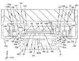
- 板状の物体を物体載置部が設けられた物体載置部材に搬送する搬送システムであって、
前記物体と対向する対向部を有し、該対向部と前記物体との間に気体流を形成して前記物体に対する吸引力を発生させる吸引部材と、
前記吸引部材によって吸引されている前記物体の形状に関する情報を求める計測装置と、
前記吸引部材を前記物体載置部に対して接近又は離間する上下方向に相対移動させる駆動装置と、
前記計測装置で求められた前記情報を用いて、前記物体が所定の形状で前記物体載置部に載置されるように前記吸引部材と前記駆動装置との少なくとも一方を制御する制御装置と、を備える搬送システム。 - 前記吸引部材は、前記対向部から気体を噴き出して前記気体流を形成する請求項1に記載の搬送システム。
- 前記制御装置は、前記物体の少なくとも一面が所定の平坦度となるように前記吸引部材と前記駆動装置との少なくとも一方を制御する請求項1又は2に記載の搬送システム。
- 前記制御装置は、前記計測装置で求められた前記情報を用いて、前記気体流を制御する請求項3に記載の搬送システム。
- 前記吸引部材は、前記一面に前記吸引力を作用させ、
前記計測装置は、前記一面の面形状に関する情報を求める請求項3又は4に記載の搬送システム。 - 前記計測装置は、前記一面と該一面に対向する前記吸引部材との間隔を測定する請求項3〜5のいずれか一項に記載の搬送システム。
- 前記計測装置は、静電容量センサを含む請求項1〜6のいずれか一項に記載の搬送システム。
- 前記計測装置は、前記物体の一面の複数個所それぞれについて前記一面と交差する方向の位置に関する情報を求める複数のセンサを有する請求項1〜7のいずれか一項に記載の搬送システム。
- 前記吸引部材は、その下面の複数箇所に配置され、それぞれ前記物体を非接触で保持する複数のチャック部材を有する請求項1〜8のいずれか一項に記載の搬送システム。
- 前記チャック部材は、ベルヌーイ効果を利用して前記物体を非接触で保持するベルヌーイ・チャックを含む請求項9に記載の搬送システム。
- 前記物体を下方から支持した状態で前記物体載置部に対して前記上下方向に相対移動可能な支持部材を更に備え、
前記制御装置は、前記計測装置で求められた前記情報を用いて、前記吸引部材の前記上下方向の移動と前記支持部材の前記上下方向の移動との少なくとも一方を制御する請求項1〜10のいずれか一項に記載の搬送システム。 - 前記支持部材は、前記物体載置部材に設けられている請求項11に記載の搬送システム。
- 前記支持部材は、前記物体を支持した状態で前記吸引部材に対して前記上下方向と交差する方向に移動可能である請求項11に記載の搬送システム。
- 前記制御装置は、前記計測装置が求めた前記情報を用いて、前記吸引部材と前記支持部材とのうちの一方の部材が前記上下方向に移動する際の移動速度を調整する請求項11〜13のいずれか一項に記載の搬送システム。
- 前記一方の部材は、前記支持部材である請求項14に記載の搬送システム。
- 前記支持部材は、前記物体の中央部を下方から支持した状態で前記物体載置部に対して前記上下方向に相対移動可能であり、
前記計測装置により前記物体の外周縁部が中央部に比べて上側に反っていることが検出された場合、前記制御装置は、前記支持部材の前記相対移動の速度を、前記吸引部材より遅くする請求項11又は12に記載の搬送システム。 - 前記支持部材は、前記物体の中央部を下方から支持した状態で前記物体載置部に対して前記上下方向に相対移動可能であり、
前記計測装置により前記物体の外周縁部が中央部に比べて下側に反っていることが検出された場合、前記制御装置は、前記支持部材の前記相対移動の速度を、前記吸引部材より速くする請求項11又は12に記載の搬送システム。 - 前記制御装置は、前記物体に対する前記吸引部材による吸引と、前記物体に対する前記支持部材による支持と、が行われている状態で前記吸引部材の前記上下方向の移動と前記支持部材の前記上下方向の移動とを制御する請求項11〜17のいずれか一項に記載の搬送システム。
- 前記吸引部材に吸引された前記物体の一部と接触するとともに、前記支持部材により前記物体が支持されたとき前記接触を解除する接触部材をさらに備える請求項11〜18のいずれか一項に記載の搬送システム。
- 前記吸引部材が上下方向に移動するときの該吸引部材の上下動をガイドし、かつ前記吸引部材の重量の少なくとも一部を支持する重量支持装置を更に備える請求項1〜19のいずれか一項に記載の搬送システム。
- 前記接触部材は、前記吸引部材の下面に対向する第1位置と前記吸引部材に対向しない第2位置との間で移動可能で、かつ前記上下方向に移動可能である請求項20に記載の搬送システム。
- 前記上下方向と交差する所定平面内での前記物体の位置に関する情報を計測する計測系をさらに備え、
前記接触部材には、反射部が設けられ、前記接触部材が前記第1位置にあるとき、前記計測系の計測光が前記反射部によって反射される請求項21に記載の搬送システム。 - 前記物体載置部材には、前記物体が前記物体載置部に載置され、前記接触部材が前記第2位置にあるとき、前記計測系の計測光を反射する第2の反射部が設けられている請求項22に記載の搬送システム。
- 前記吸引部材により保持されるのに先だって、前記物体載置部材の上方の前記吸引部材の下方に、前記物体を搬送する搬送部材をさらに備える請求項1〜23のいずれか一項に記載の搬送システム。
- 物体上にパターンを形成する露光装置であって、
請求項1〜24のいずれか一項に記載の搬送システムと、
前記搬送システムにより前記物体載置部材上に搬送された前記物体をエネルギビームで露光して、前記パターンを形成するパターン生成装置と、を備える露光装置。 - 前記パターン生成装置は、前記エネルギビームを前記物体に向けて射出する光学系を含み、
前記吸引部材は、前記光学系とは振動的に分離されている請求項25に記載の露光装置。 - 請求項25又は26に記載の露光装置を用いて物体を露光することと、
露光された前記物体を現像することと、を含むデバイス製造方法。 - 板状の物体を物体載置部が設けられた物体載置部材に搬送する搬送方法であって、
前記物体載置部材の上方にて、吸引部材により前記物体を上方から非接触で吸引することと、
駆動装置によって前記吸引部材を前記物体載置部に対して上下方向に相対移動させること、
前記吸引部材によって吸引された前記物体の複数個所に関し、それぞれ前記上下方向の位置に関する情報を求めることと、
求められた前記情報を用いて、前記物体が所定の形状で前記物体載置部に載置されるように前記吸引部材と前記駆動装置との少なくとも一方を制御することと、を含む搬送方法。 - 前記物体を支持部材によって下方から支持した状態で前記物体載置部に対して前記上下方向に相対移動させること、を更に含み、
前記制御することでは、求められた前記情報を用いて、前記吸引部材の前記上下方向の移動と前記支持部材の前記上下方向の移動との少なくとも一方を制御する請求項28に記載の搬送方法。 - 前記制御することでは、前記複数の位置に関する情報が所定値となるように、前記吸引部材の前記上下方向の移動と前記支持部材の前記上下方向の移動とを独立に制御する請求項29に記載の搬送方法。
- 前記複数の位置に関する情報は、前記物体の中央部側の少なくとも1点と外周部近傍の少なくとも3点とを含む複数点で求められる請求項30に記載の搬送方法。
- 前記制御することでは、前記情報に基づいて、前記吸引部材と前記支持部材とのうちの一方の部材が上下方向に移動する際の移動速度を制御する請求項28〜31のいずれか一項に記載の搬送方法。
- 前記支持部材によって前記物体を支持するのに先立って、吸引部材により吸引されている前記物体の一部を接触部材に接触させることと、
前記物体が前記支持部材により下方から支持された後、前記接触部材による前記物体に対する接触を解除することと、をさらに含む請求項29〜32のいずれか一項に記載の搬送方法。 - 前記吸引部材及び前記支持部材が下降中に、前記物体の前記上下方向と交差する所定平面内の位置情報を計測することをさらに含む請求項29〜33のいずれか一項に記載の搬送方法。
- 前記吸引部材により保持されるのに先だって、前記物体載置部材の上方でかつ前記吸引部材の下方に、搬送部材により前記物体を搬送することをさらに含む請求項28〜34のいずれか一項に記載の搬送方法。
- 請求項28〜35のいずれか一項に記載の搬送方法によって前記物体載置部材上に板状の前記物体を搬送することと、
搬送後に前記物体載置部材に保持されている前記物体をエネルギビームで露光し、前記物体上にパターンを形成することと、を含む露光方法。 - 請求項36に記載の露光方法により物体を露光することと、
露光された前記物体を現像することと、を含むデバイス製造方法。 - 板状の物体を吸引する吸引装置であって、
前記物体と対向する対向部を有し、該対向部から気体を噴き出して前記物体に対する吸引力を発生させる吸引部材と、
前記吸引部材によって吸引されている前記物体の形状に関する情報を求める計測装置と、
前記計測装置で求められた情報を用いて前記気体の流れを制御する制御装置と、を備える吸引装置。 - 前記吸引部材は、前記物体の一面に前記吸引力を作用させ、
前記計測装置は、前記物体の一面の面形状に関する情報を求める請求項38に記載の吸引装置。 - 前記計測装置は、前記物体の一面と該一面と対向する前記吸引部材との間隔を測定する請求項38又は39に記載の吸引装置。
- 前記計測装置は、静電容量センサを含む請求項40に記載の吸引装置。
- 前記計測装置は、前記物体の一面の複数個所それぞれについて前記一面と交差する方向の位置に関する情報を求める複数のセンサを有する請求項38又は39に記載の吸引装置。
- 前記制御装置は、前記気体の流れを制御して前記物体の形状を所定の状態にする請求項38〜42のいずれか一項に記載の吸引装置。
Applications Claiming Priority (3)
| Application Number | Priority Date | Filing Date | Title |
|---|---|---|---|
| US201261731892P | 2012-11-30 | 2012-11-30 | |
| US61/731,892 | 2012-11-30 | ||
| PCT/JP2013/081852 WO2014084229A1 (ja) | 2012-11-30 | 2013-11-27 | 搬送システム、露光装置、搬送方法、露光方法及びデバイス製造方法、並びに吸引装置 |
Related Child Applications (1)
| Application Number | Title | Priority Date | Filing Date |
|---|---|---|---|
| JP2018107671A Division JP6607286B2 (ja) | 2012-11-30 | 2018-06-05 | 搬送システム、露光装置、搬送方法、露光方法及びデバイス製造方法 |
Publications (2)
| Publication Number | Publication Date |
|---|---|
| JPWO2014084229A1 JPWO2014084229A1 (ja) | 2017-01-05 |
| JP6358564B2 true JP6358564B2 (ja) | 2018-07-18 |
Family
ID=50827865
Family Applications (6)
| Application Number | Title | Priority Date | Filing Date |
|---|---|---|---|
| JP2014550208A Active JP6358564B2 (ja) | 2012-11-30 | 2013-11-27 | 搬送システム、露光装置、搬送方法、露光方法及びデバイス製造方法、並びに吸引装置 |
| JP2018107671A Active JP6607286B2 (ja) | 2012-11-30 | 2018-06-05 | 搬送システム、露光装置、搬送方法、露光方法及びデバイス製造方法 |
| JP2019189302A Active JP6981458B2 (ja) | 2012-11-30 | 2019-10-16 | 搬送システム、露光装置、搬送方法、露光方法及びデバイス製造方法 |
| JP2021186320A Active JP7243797B2 (ja) | 2012-11-30 | 2021-11-16 | 搬送システム、露光装置、及び搬送方法 |
| JP2023032530A Pending JP2023078199A (ja) | 2012-11-30 | 2023-03-03 | 搬送システム、露光装置、及び搬送方法 |
| JP2024209537A Active JP7758139B2 (ja) | 2012-11-30 | 2024-12-02 | 搬送システム、露光装置、及び搬送方法 |
Family Applications After (5)
| Application Number | Title | Priority Date | Filing Date |
|---|---|---|---|
| JP2018107671A Active JP6607286B2 (ja) | 2012-11-30 | 2018-06-05 | 搬送システム、露光装置、搬送方法、露光方法及びデバイス製造方法 |
| JP2019189302A Active JP6981458B2 (ja) | 2012-11-30 | 2019-10-16 | 搬送システム、露光装置、搬送方法、露光方法及びデバイス製造方法 |
| JP2021186320A Active JP7243797B2 (ja) | 2012-11-30 | 2021-11-16 | 搬送システム、露光装置、及び搬送方法 |
| JP2023032530A Pending JP2023078199A (ja) | 2012-11-30 | 2023-03-03 | 搬送システム、露光装置、及び搬送方法 |
| JP2024209537A Active JP7758139B2 (ja) | 2012-11-30 | 2024-12-02 | 搬送システム、露光装置、及び搬送方法 |
Country Status (8)
| Country | Link |
|---|---|
| US (6) | US9821469B2 (ja) |
| EP (2) | EP2950329B1 (ja) |
| JP (6) | JP6358564B2 (ja) |
| KR (4) | KR102523729B1 (ja) |
| CN (4) | CN104956465B (ja) |
| HK (1) | HK1216357A1 (ja) |
| TW (4) | TWI667725B (ja) |
| WO (1) | WO2014084229A1 (ja) |
Families Citing this family (39)
| Publication number | Priority date | Publication date | Assignee | Title |
|---|---|---|---|---|
| WO2014084229A1 (ja) | 2012-11-30 | 2014-06-05 | 株式会社ニコン | 搬送システム、露光装置、搬送方法、露光方法及びデバイス製造方法、並びに吸引装置 |
| JP6286024B2 (ja) * | 2014-03-07 | 2018-02-28 | 富士フイルム株式会社 | トランジスタの製造方法 |
| GB2530982B (en) * | 2014-09-30 | 2018-10-24 | M Solv Ltd | Bernoulli process head |
| JP6485687B2 (ja) * | 2014-12-25 | 2019-03-20 | 株式会社ニコン | 保持装置、物体支持装置及び露光装置、並びにデバイス製造方法 |
| KR101657079B1 (ko) * | 2015-03-16 | 2016-09-13 | 주식회사 테스 | 기판처리장치의 수평조절장치 및 이를 이용한 수평조절방법 |
| US9929121B2 (en) * | 2015-08-31 | 2018-03-27 | Kulicke And Soffa Industries, Inc. | Bonding machines for bonding semiconductor elements, methods of operating bonding machines, and techniques for improving UPH on such bonding machines |
| CN105159035B (zh) * | 2015-09-22 | 2018-05-18 | 上海华力微电子有限公司 | 一种改善晶圆形变的曝光载片台 |
| JP6587138B2 (ja) * | 2015-12-02 | 2019-10-09 | 株式会社ニコン | 物体支持装置及び露光装置 |
| JP6568828B2 (ja) * | 2016-08-01 | 2019-08-28 | 株式会社Kokusai Electric | ティーチング治具、基板処理装置及びティーチング方法 |
| JP6689160B2 (ja) * | 2016-08-24 | 2020-04-28 | 株式会社ディスコ | 板状物搬送装置及び加工装置 |
| KR20220138030A (ko) * | 2016-11-09 | 2022-10-12 | 도쿄엘렉트론가부시키가이샤 | 접합 장치, 접합 시스템, 접합 방법 및 컴퓨터 기억 매체 |
| KR101898073B1 (ko) * | 2016-11-29 | 2018-09-17 | 주식회사 이오테크닉스 | 레이저 마킹 장치 및 이에 사용되는 관절 구조물 보관 장치 |
| JP6797063B2 (ja) * | 2017-04-14 | 2020-12-09 | 東京エレクトロン株式会社 | ピン制御方法及び基板処理装置 |
| US11360400B2 (en) | 2017-05-19 | 2022-06-14 | Massachusetts Institute Of Technology | Transport system having a magnetically levitated transportation stage |
| US10522385B2 (en) * | 2017-09-26 | 2019-12-31 | Taiwan Semiconductor Manufacturing Co., Ltd. | Wafer table with dynamic support pins |
| JP7009306B2 (ja) * | 2018-05-21 | 2022-01-25 | 株式会社ディスコ | 切削装置 |
| KR20190134275A (ko) | 2018-05-25 | 2019-12-04 | 주식회사 넥서스원 | 웨이퍼의 에지 영역 검사 시스템 및 검사 방법 |
| US10831110B2 (en) * | 2018-05-29 | 2020-11-10 | Taiwan Semiconductor Manufacturing Company Ltd. | Lithographic overlay correction and lithographic process |
| JP7110005B2 (ja) * | 2018-06-20 | 2022-08-01 | キヤノン株式会社 | 基板回転装置、基板回転方法、リソグラフィ装置、および物品製造方法 |
| US10763154B2 (en) * | 2018-08-28 | 2020-09-01 | Applied Materials, Inc. | Measurement of flatness of a susceptor of a display CVD chamber |
| JP7267111B2 (ja) * | 2019-05-31 | 2023-05-01 | 東京エレクトロン株式会社 | 位置決め機構及び位置決め方法 |
| US11209373B2 (en) * | 2019-06-21 | 2021-12-28 | Kla Corporation | Six degree of freedom workpiece stage |
| JP6822534B2 (ja) * | 2019-09-12 | 2021-01-27 | 株式会社ニコン | 物体支持装置及び露光装置 |
| JP7149249B2 (ja) * | 2019-10-31 | 2022-10-06 | Towa株式会社 | 搬送モジュール、切断装置及び切断品の製造方法 |
| JP7419030B2 (ja) * | 2019-11-18 | 2024-01-22 | キヤノン株式会社 | 保持装置、露光装置、及び物品の製造方法 |
| CN113050380B (zh) * | 2019-12-27 | 2021-12-10 | 上海微电子装备(集团)股份有限公司 | 浸没头的集成工装及其集成方法和光刻机 |
| KR102136084B1 (ko) | 2020-06-16 | 2020-08-13 | 주식회사 넥서스원 | 웨이퍼의 에지 영역 검사 시스템 |
| KR102136085B1 (ko) | 2020-06-16 | 2020-07-23 | 주식회사 넥서스원 | 웨이퍼의 에지 영역 검사장치 |
| US11740564B2 (en) * | 2020-06-18 | 2023-08-29 | Taiwan Semiconductor Manufacturing Company, Ltd. | Lithography apparatus and method using the same |
| JP7608106B2 (ja) * | 2020-10-05 | 2025-01-06 | キオクシア株式会社 | 半導体製造装置 |
| CN116250073A (zh) * | 2020-10-08 | 2023-06-09 | Asml荷兰有限公司 | 衬底保持器、包括衬底保持器的承载件系统、和光刻设备 |
| US11551970B2 (en) * | 2020-10-22 | 2023-01-10 | Innolux Corporation | Method for manufacturing an electronic device |
| US20230395409A1 (en) * | 2020-11-13 | 2023-12-07 | Massachusetts Institute Of Technology | Reticle exchange device with reticle levitation |
| EP4105720A1 (en) * | 2021-06-16 | 2022-12-21 | ASML Netherlands B.V. | Substrate holder and method |
| JP7698543B2 (ja) * | 2021-09-28 | 2025-06-25 | キヤノン株式会社 | ステージ装置、リソグラフィ装置及び物品の製造方法 |
| CN114505817B (zh) * | 2022-03-11 | 2024-04-19 | 深圳市凯威达电子有限公司 | 一种智能照明驱动芯片生产用可精准定位的插接装置 |
| CN115057233B (zh) * | 2022-06-09 | 2024-01-09 | 河北光兴半导体技术有限公司 | 一种掰断装置及掰断方法 |
| CN115547915B (zh) * | 2022-11-28 | 2023-02-14 | 四川上特科技有限公司 | 一种晶圆曝光夹具及曝光装置 |
| JP7681200B1 (ja) * | 2024-02-28 | 2025-05-21 | キヤノン株式会社 | 基板保持装置、基板処理装置、基板保持方法、基板処理方法、および物品製造方法 |
Family Cites Families (90)
| Publication number | Priority date | Publication date | Assignee | Title |
|---|---|---|---|---|
| DE3110341C2 (de) * | 1980-03-19 | 1983-11-17 | Hitachi, Ltd., Tokyo | Verfahren und Vorrichtung zum Ausrichten eines dünnen Substrats in der Bildebene eines Kopiergerätes |
| JPS57117238A (en) | 1981-01-14 | 1982-07-21 | Nippon Kogaku Kk <Nikon> | Exposing and baking device for manufacturing integrated circuit with illuminometer |
| JPH0669027B2 (ja) * | 1983-02-21 | 1994-08-31 | 株式会社日立製作所 | 半導体ウエハの薄膜形成方法 |
| JPS63260129A (ja) * | 1987-04-17 | 1988-10-27 | Hitachi Electronics Eng Co Ltd | 露光装置 |
| US5196745A (en) | 1991-08-16 | 1993-03-23 | Massachusetts Institute Of Technology | Magnetic positioning device |
| JPH05102287A (ja) * | 1991-10-02 | 1993-04-23 | Hitachi Ltd | 板状物搬送装置 |
| JPH06302550A (ja) | 1993-04-13 | 1994-10-28 | Hitachi Ltd | 半導体製造装置 |
| US6624433B2 (en) | 1994-02-22 | 2003-09-23 | Nikon Corporation | Method and apparatus for positioning substrate and the like |
| SG102627A1 (en) | 1996-11-28 | 2004-03-26 | Nikon Corp | Lithographic device |
| WO1998028665A1 (en) | 1996-12-24 | 1998-07-02 | Koninklijke Philips Electronics N.V. | Two-dimensionally balanced positioning device with two object holders, and lithographic device provided with such a positioning device |
| EP0866375A3 (en) * | 1997-03-17 | 2000-05-24 | Nikon Corporation | Article positioning apparatus and exposing apparatus having the same |
| JPH10256355A (ja) * | 1997-03-17 | 1998-09-25 | Nikon Corp | 位置決めデバイス、基板保持装置、及び該装置を備えた露光装置 |
| JPH1116816A (ja) | 1997-06-25 | 1999-01-22 | Nikon Corp | 投影露光装置、該装置を用いた露光方法、及び該装置を用いた回路デバイスの製造方法 |
| US6208407B1 (en) | 1997-12-22 | 2001-03-27 | Asm Lithography B.V. | Method and apparatus for repetitively projecting a mask pattern on a substrate, using a time-saving height measurement |
| KR100841147B1 (ko) | 1998-03-11 | 2008-06-24 | 가부시키가이샤 니콘 | 레이저 장치, 자외광 조사 장치 및 방법, 물체의 패턴 검출장치 및 방법 |
| EP1077393A2 (en) * | 1999-08-19 | 2001-02-21 | Canon Kabushiki Kaisha | Substrate attracting and holding system for use in exposure apparatus |
| US6771350B2 (en) | 2000-02-25 | 2004-08-03 | Nikon Corporation | Exposure apparatus and exposure method capable of controlling illumination distribution |
| JP2001332609A (ja) * | 2000-03-13 | 2001-11-30 | Nikon Corp | 基板保持装置及び露光装置 |
| US20020041377A1 (en) | 2000-04-25 | 2002-04-11 | Nikon Corporation | Aerial image measurement method and unit, optical properties measurement method and unit, adjustment method of projection optical system, exposure method and apparatus, making method of exposure apparatus, and device manufacturing method |
| KR100855527B1 (ko) * | 2001-02-13 | 2008-09-01 | 가부시키가이샤 니콘 | 유지장치, 유지방법, 노광장치 및 디바이스 제조방법 |
| EP1364257A1 (en) | 2001-02-27 | 2003-11-26 | ASML US, Inc. | Simultaneous imaging of two reticles |
| JP3761444B2 (ja) * | 2001-10-23 | 2006-03-29 | 富士通株式会社 | 半導体装置の製造方法 |
| JP4018958B2 (ja) * | 2001-10-30 | 2007-12-05 | 大日本スクリーン製造株式会社 | 基板処理装置 |
| KR100927560B1 (ko) | 2002-01-29 | 2009-11-23 | 가부시키가이샤 니콘 | 이미지 형성 상태 조정 시스템, 노광 방법 및 노광 장치, 그리고 프로그램 및 정보 기록 매체 |
| JP4353454B2 (ja) | 2002-06-21 | 2009-10-28 | 大日本スクリーン製造株式会社 | 熱処理装置 |
| JP3920720B2 (ja) * | 2002-03-29 | 2007-05-30 | 株式会社荏原製作所 | 基板受渡し方法、基板受渡し機構及び基板研磨装置 |
| JP2003297901A (ja) * | 2002-04-05 | 2003-10-17 | Supurauto:Kk | 基板処理システムおよびその処理方法 |
| CN1296261C (zh) * | 2002-06-22 | 2007-01-24 | 鸿富锦精密工业(深圳)有限公司 | 真空夹具及其使用方法 |
| JP2004158847A (ja) * | 2002-10-17 | 2004-06-03 | Advanced Lcd Technologies Development Center Co Ltd | 薄い基板上にパターンを形成する装置およびその方法 |
| CN101241317B (zh) * | 2002-12-10 | 2010-11-17 | 株式会社尼康 | 曝光装置以及器件制造方法 |
| JP2004235622A (ja) * | 2003-01-09 | 2004-08-19 | Disco Abrasive Syst Ltd | 板状物の搬送装置 |
| JP2004296777A (ja) * | 2003-03-27 | 2004-10-21 | Oki Electric Ind Co Ltd | ワーク吸着装置及びワーク吸着方法 |
| JP4023543B2 (ja) * | 2003-05-29 | 2007-12-19 | 東京エレクトロン株式会社 | 基板搬送装置および基板搬送方法ならびに真空処理装置 |
| JP4754196B2 (ja) * | 2003-08-25 | 2011-08-24 | 東京エレクトロン株式会社 | 減圧処理室内の部材清浄化方法および基板処理装置 |
| JP4130167B2 (ja) * | 2003-10-06 | 2008-08-06 | 日東電工株式会社 | 半導体ウエハの剥離方法 |
| CN100445049C (zh) * | 2003-11-21 | 2008-12-24 | 三星钻石工业股份有限公司 | 真空吸头、使用该真空吸头的真空吸附装置和工作台 |
| EP2717295B1 (en) | 2003-12-03 | 2018-07-18 | Nikon Corporation | Exposure apparatus, exposure method, and method for producing a device |
| KR101111363B1 (ko) | 2003-12-15 | 2012-04-12 | 가부시키가이샤 니콘 | 투영노광장치 및 스테이지 장치, 그리고 노광방법 |
| JP4575727B2 (ja) | 2004-08-23 | 2010-11-04 | 川崎重工業株式会社 | 基板状態検出装置、ロボットハンド及び基板搬送用ロボット |
| JP4495552B2 (ja) | 2004-09-09 | 2010-07-07 | 萩原エンジニアリング株式会社 | 搬送装置 |
| JP4541824B2 (ja) * | 2004-10-14 | 2010-09-08 | リンテック株式会社 | 非接触型吸着保持装置 |
| JP4570037B2 (ja) * | 2005-03-17 | 2010-10-27 | 株式会社アルバック | 基板搬送システム |
| JP2007114570A (ja) * | 2005-10-21 | 2007-05-10 | Nikon Corp | 基板ホルダ、露光装置及びデバイスの製造方法 |
| US7643130B2 (en) * | 2005-11-04 | 2010-01-05 | Nuflare Technology, Inc. | Position measuring apparatus and positional deviation measuring method |
| JP2007214336A (ja) * | 2006-02-09 | 2007-08-23 | Nikon Corp | 保持装置、保持方法、ステージ装置、露光装置、デバイスの製造方法 |
| CN101980084B (zh) | 2006-02-21 | 2013-01-23 | 株式会社尼康 | 曝光装置、曝光方法及组件制造方法 |
| US7659964B2 (en) | 2006-03-28 | 2010-02-09 | Taiwan Semiconductor Manufacturing Co., Ltd. | Level adjustment systems and adjustable pin chuck thereof |
| JP2007299864A (ja) * | 2006-04-28 | 2007-11-15 | Nikon Corp | 保持方法及び保持装置、パターン形成方法及びパターン形成装置、デバイス製造方法 |
| JP4642787B2 (ja) * | 2006-05-09 | 2011-03-02 | 東京エレクトロン株式会社 | 基板搬送装置及び縦型熱処理装置 |
| EP1865220B1 (de) * | 2006-06-10 | 2014-03-19 | Integrated Dynamics Engineering GmbH | Aktives Schwingungsisolationssystem mit verbesserter Wirkung gegen seismische Schwingungen |
| JP2008047696A (ja) * | 2006-08-16 | 2008-02-28 | Disco Abrasive Syst Ltd | ウエーハ搬送方法および研削装置 |
| TWI547771B (zh) | 2006-08-31 | 2016-09-01 | 尼康股份有限公司 | Mobile body drive system and moving body driving method, pattern forming apparatus and method, exposure apparatus and method, component manufacturing method, and method of determining |
| KR101011491B1 (ko) * | 2006-11-02 | 2011-01-31 | 도쿄엘렉트론가부시키가이샤 | 미소 구조체의 검사 장치, 미소 구조체의 검사 방법 및 기판 유지 장치 |
| WO2008056735A1 (en) | 2006-11-09 | 2008-05-15 | Nikon Corporation | Holding unit, position detecting system and exposure system, moving method, position detecting method, exposure method, adjusting method of detection system, and device producing method |
| JP5080090B2 (ja) * | 2007-01-15 | 2012-11-21 | リンテック株式会社 | 保持装置及び保持方法 |
| JP4564022B2 (ja) * | 2007-01-16 | 2010-10-20 | 東京エレクトロン株式会社 | 基板搬送装置及び縦型熱処理装置 |
| JP4740414B2 (ja) * | 2007-04-24 | 2011-08-03 | 東京エレクトロン株式会社 | 基板搬送装置 |
| JP2008288347A (ja) * | 2007-05-16 | 2008-11-27 | Canon Inc | 露光装置及びデバイス製造方法 |
| KR100877102B1 (ko) | 2007-05-28 | 2009-01-09 | 주식회사 하이닉스반도체 | 열처리 장치 및 이를 이용한 열처리 방법 |
| KR101232234B1 (ko) * | 2007-06-21 | 2013-02-12 | 에이에스엠엘 네델란즈 비.브이. | 클램핑 디바이스 및 대상물 로딩 방법 |
| JP2009028863A (ja) * | 2007-07-27 | 2009-02-12 | Ihi Corp | 非接触搬送装置 |
| JP2009049119A (ja) * | 2007-08-17 | 2009-03-05 | Nikon Corp | ベース部材とその製造方法及びステージ装置並びに露光装置 |
| JP4922870B2 (ja) * | 2007-08-31 | 2012-04-25 | 株式会社アルバック | 基板リフト装置 |
| NL1036290A1 (nl) | 2007-12-19 | 2009-06-22 | Asml Netherlands Bv | Lithographic apparatus. |
| JP5241276B2 (ja) * | 2008-03-10 | 2013-07-17 | キヤノン株式会社 | 露光装置 |
| JP4983661B2 (ja) * | 2008-03-14 | 2012-07-25 | 富士通セミコンダクター株式会社 | 半導体装置の製造方法 |
| DE102008023907A1 (de) * | 2008-05-16 | 2009-12-03 | Innolas Systems Gmbh | Bernoulli-Greifvorrichtung zum Greifen und Handhaben von plattenförmigen Elementen, insbesondere von Waferelementen |
| KR101227918B1 (ko) | 2008-05-22 | 2013-01-30 | 무라다기카이가부시끼가이샤 | 천정반송차 |
| US20090311419A1 (en) * | 2008-06-12 | 2009-12-17 | Anita Foerster | Method and apparatus for resist development |
| JP5261085B2 (ja) | 2008-09-05 | 2013-08-14 | 東京エレクトロン株式会社 | 基板載置機構、基板処理装置、基板載置機構の制御方法及び記憶媒体 |
| JP2010067867A (ja) * | 2008-09-11 | 2010-03-25 | Nikon Corp | 露光方法及び装置、並びにデバイス製造方法 |
| US8325325B2 (en) | 2008-09-22 | 2012-12-04 | Nikon Corporation | Movable body apparatus, movable body drive method, exposure apparatus, exposure method, and device manufacturing method |
| US8994923B2 (en) | 2008-09-22 | 2015-03-31 | Nikon Corporation | Movable body apparatus, exposure apparatus, exposure method, and device manufacturing method |
| JP5287491B2 (ja) * | 2009-05-18 | 2013-09-11 | 株式会社島津製作所 | 基板吸着装置 |
| US8970820B2 (en) * | 2009-05-20 | 2015-03-03 | Nikon Corporation | Object exchange method, exposure method, carrier system, exposure apparatus, and device manufacturing method |
| US20100313954A1 (en) | 2009-06-16 | 2010-12-16 | Emcore Solar Power, Inc. | Concentrated Photovoltaic System Receiver for III-V Semiconductor Solar Cells |
| US20110085150A1 (en) | 2009-09-30 | 2011-04-14 | Nikon Corporation | Exposure apparatus, exposure method, and device manufacturing method |
| US20110123913A1 (en) * | 2009-11-19 | 2011-05-26 | Nikon Corporation | Exposure apparatus, exposing method, and device fabricating method |
| JP5683930B2 (ja) * | 2010-01-29 | 2015-03-11 | Hoya株式会社 | マスクブランク用基板、マスクブランク、転写用マスク及び半導体デバイスの製造方法 |
| KR102172551B1 (ko) * | 2010-02-17 | 2020-11-02 | 가부시키가이샤 니콘 | 반송 장치, 반송 방법, 노광 장치, 및 디바이스 제조 방법 |
| JP2012038874A (ja) * | 2010-08-06 | 2012-02-23 | Hitachi High-Technologies Corp | 液晶露光装置 |
| US20120064460A1 (en) | 2010-09-07 | 2012-03-15 | Nikon Corporation | Movable body apparatus, object processing device, exposure apparatus, flat-panel display manufacturing method, and device manufacturing method |
| NL2007634A (en) * | 2010-12-13 | 2012-06-15 | Asml Netherlands Bv | Lithographic apparatus and method. |
| JP5323867B2 (ja) * | 2011-01-19 | 2013-10-23 | 東京エレクトロン株式会社 | 基板反転装置、基板反転方法、剥離システム、プログラム及びコンピュータ記憶媒体 |
| JP5963453B2 (ja) * | 2011-03-15 | 2016-08-03 | 株式会社荏原製作所 | 検査装置 |
| WO2012140988A1 (ja) * | 2011-04-12 | 2012-10-18 | 東京エレクトロン株式会社 | 剥離方法、剥離装置及び剥離システム |
| CN103199049B (zh) * | 2012-01-04 | 2015-09-09 | 沈阳芯源微电子设备有限公司 | 一种可兼容不同尺寸晶圆的伯努利承片台 |
| JP5952059B2 (ja) * | 2012-04-04 | 2016-07-13 | 東京エレクトロン株式会社 | 基板処理装置および基板保持方法 |
| KR101390391B1 (ko) * | 2012-05-21 | 2014-05-27 | 엔젯 주식회사 | 정전기력을 이용하는 3차원 형상 표면 인쇄장치 |
| WO2014084229A1 (ja) | 2012-11-30 | 2014-06-05 | 株式会社ニコン | 搬送システム、露光装置、搬送方法、露光方法及びデバイス製造方法、並びに吸引装置 |
-
2013
- 2013-11-27 WO PCT/JP2013/081852 patent/WO2014084229A1/ja not_active Ceased
- 2013-11-27 KR KR1020227007257A patent/KR102523729B1/ko active Active
- 2013-11-27 KR KR1020157017386A patent/KR102211380B1/ko active Active
- 2013-11-27 CN CN201380071862.7A patent/CN104956465B/zh active Active
- 2013-11-27 CN CN202110238869.XA patent/CN113035768B/zh active Active
- 2013-11-27 EP EP13859307.4A patent/EP2950329B1/en active Active
- 2013-11-27 CN CN202410408382.5A patent/CN118280908A/zh active Pending
- 2013-11-27 KR KR1020217002828A patent/KR102373075B1/ko active Active
- 2013-11-27 US US14/648,280 patent/US9821469B2/en active Active
- 2013-11-27 JP JP2014550208A patent/JP6358564B2/ja active Active
- 2013-11-27 EP EP21209861.0A patent/EP4009356A1/en active Pending
- 2013-11-27 CN CN201810418024.7A patent/CN108732871B/zh active Active
- 2013-11-27 HK HK16104043.1A patent/HK1216357A1/en unknown
- 2013-11-27 KR KR1020237012898A patent/KR102744481B1/ko active Active
- 2013-11-29 TW TW106136125A patent/TWI667725B/zh active
- 2013-11-29 TW TW108122353A patent/TWI703666B/zh active
- 2013-11-29 TW TW102143679A patent/TWI606540B/zh active
- 2013-11-29 TW TW109124507A patent/TWI748563B/zh active
-
2017
- 2017-06-29 US US15/637,069 patent/US10081108B2/en active Active
-
2018
- 2018-05-09 US US15/974,965 patent/US10384350B2/en active Active
- 2018-06-05 JP JP2018107671A patent/JP6607286B2/ja active Active
-
2019
- 2019-06-20 US US16/446,979 patent/US10744648B2/en active Active
- 2019-10-16 JP JP2019189302A patent/JP6981458B2/ja active Active
-
2020
- 2020-07-10 US US16/925,386 patent/US11097426B2/en active Active
-
2021
- 2021-07-21 US US17/381,491 patent/US11511438B2/en active Active
- 2021-11-16 JP JP2021186320A patent/JP7243797B2/ja active Active
-
2023
- 2023-03-03 JP JP2023032530A patent/JP2023078199A/ja active Pending
-
2024
- 2024-12-02 JP JP2024209537A patent/JP7758139B2/ja active Active
Also Published As
Similar Documents
| Publication | Publication Date | Title |
|---|---|---|
| JP7243797B2 (ja) | 搬送システム、露光装置、及び搬送方法 | |
| CN108336011B (zh) | 搬入方法、搬送系统及曝光装置、和器件制造方法 |
Legal Events
| Date | Code | Title | Description |
|---|---|---|---|
| A621 | Written request for application examination |
Free format text: JAPANESE INTERMEDIATE CODE: A621 Effective date: 20161102 |
|
| A131 | Notification of reasons for refusal |
Free format text: JAPANESE INTERMEDIATE CODE: A131 Effective date: 20170627 |
|
| A601 | Written request for extension of time |
Free format text: JAPANESE INTERMEDIATE CODE: A601 Effective date: 20170825 |
|
| A521 | Request for written amendment filed |
Free format text: JAPANESE INTERMEDIATE CODE: A523 Effective date: 20171012 |
|
| A131 | Notification of reasons for refusal |
Free format text: JAPANESE INTERMEDIATE CODE: A131 Effective date: 20180207 |
|
| A601 | Written request for extension of time |
Free format text: JAPANESE INTERMEDIATE CODE: A601 Effective date: 20180409 |
|
| A521 | Request for written amendment filed |
Free format text: JAPANESE INTERMEDIATE CODE: A523 Effective date: 20180518 |
|
| TRDD | Decision of grant or rejection written | ||
| A01 | Written decision to grant a patent or to grant a registration (utility model) |
Free format text: JAPANESE INTERMEDIATE CODE: A01 Effective date: 20180528 |
|
| R150 | Certificate of patent or registration of utility model |
Ref document number: 6358564 Country of ref document: JP Free format text: JAPANESE INTERMEDIATE CODE: R150 |
|
| A61 | First payment of annual fees (during grant procedure) |
Free format text: JAPANESE INTERMEDIATE CODE: A61 Effective date: 20180610 |
|
| R250 | Receipt of annual fees |
Free format text: JAPANESE INTERMEDIATE CODE: R250 |
|
| R250 | Receipt of annual fees |
Free format text: JAPANESE INTERMEDIATE CODE: R250 |
|
| R250 | Receipt of annual fees |
Free format text: JAPANESE INTERMEDIATE CODE: R250 |
|
| R250 | Receipt of annual fees |
Free format text: JAPANESE INTERMEDIATE CODE: R250 |
|
| R250 | Receipt of annual fees |
Free format text: JAPANESE INTERMEDIATE CODE: R250 |