JP5957553B2 - Semiconductor device - Google Patents
Semiconductor device Download PDFInfo
- Publication number
- JP5957553B2 JP5957553B2 JP2015033863A JP2015033863A JP5957553B2 JP 5957553 B2 JP5957553 B2 JP 5957553B2 JP 2015033863 A JP2015033863 A JP 2015033863A JP 2015033863 A JP2015033863 A JP 2015033863A JP 5957553 B2 JP5957553 B2 JP 5957553B2
- Authority
- JP
- Japan
- Prior art keywords
- transistor
- oxide semiconductor
- semiconductor layer
- electrode
- insulating layer
- Prior art date
- Legal status (The legal status is an assumption and is not a legal conclusion. Google has not performed a legal analysis and makes no representation as to the accuracy of the status listed.)
- Expired - Fee Related
Links
- 239000004065 semiconductor Substances 0.000 title claims description 535
- 239000003990 capacitor Substances 0.000 claims description 112
- 230000015572 biosynthetic process Effects 0.000 claims description 82
- 239000013078 crystal Substances 0.000 claims description 42
- 229910052710 silicon Inorganic materials 0.000 claims description 37
- 239000010703 silicon Substances 0.000 claims description 37
- 229910052733 gallium Inorganic materials 0.000 claims description 23
- 229910052725 zinc Inorganic materials 0.000 claims description 8
- 229910052738 indium Inorganic materials 0.000 claims description 6
- 239000010410 layer Substances 0.000 description 608
- 238000010438 heat treatment Methods 0.000 description 129
- 239000000463 material Substances 0.000 description 101
- 239000000758 substrate Substances 0.000 description 95
- 238000000034 method Methods 0.000 description 92
- 239000010408 film Substances 0.000 description 89
- 239000001257 hydrogen Substances 0.000 description 77
- 229910052739 hydrogen Inorganic materials 0.000 description 77
- 229910052760 oxygen Inorganic materials 0.000 description 68
- 239000012298 atmosphere Substances 0.000 description 63
- 239000001301 oxygen Substances 0.000 description 62
- QVGXLLKOCUKJST-UHFFFAOYSA-N atomic oxygen Chemical compound [O] QVGXLLKOCUKJST-UHFFFAOYSA-N 0.000 description 61
- 239000011229 interlayer Substances 0.000 description 61
- 239000012535 impurity Substances 0.000 description 60
- UFHFLCQGNIYNRP-UHFFFAOYSA-N Hydrogen Chemical compound [H][H] UFHFLCQGNIYNRP-UHFFFAOYSA-N 0.000 description 59
- 239000007789 gas Substances 0.000 description 57
- 229910007541 Zn O Inorganic materials 0.000 description 50
- XKRFYHLGVUSROY-UHFFFAOYSA-N Argon Chemical compound [Ar] XKRFYHLGVUSROY-UHFFFAOYSA-N 0.000 description 48
- 238000005530 etching Methods 0.000 description 45
- XUIMIQQOPSSXEZ-UHFFFAOYSA-N Silicon Chemical compound [Si] XUIMIQQOPSSXEZ-UHFFFAOYSA-N 0.000 description 36
- XLYOFNOQVPJJNP-UHFFFAOYSA-N water Substances O XLYOFNOQVPJJNP-UHFFFAOYSA-N 0.000 description 35
- 229910001868 water Inorganic materials 0.000 description 35
- XLOMVQKBTHCTTD-UHFFFAOYSA-N Zinc monoxide Chemical compound [Zn]=O XLOMVQKBTHCTTD-UHFFFAOYSA-N 0.000 description 34
- IJGRMHOSHXDMSA-UHFFFAOYSA-N Atomic nitrogen Chemical compound N#N IJGRMHOSHXDMSA-UHFFFAOYSA-N 0.000 description 33
- 239000010936 titanium Substances 0.000 description 29
- 229910052719 titanium Inorganic materials 0.000 description 28
- RTAQQCXQSZGOHL-UHFFFAOYSA-N Titanium Chemical compound [Ti] RTAQQCXQSZGOHL-UHFFFAOYSA-N 0.000 description 27
- 238000004544 sputter deposition Methods 0.000 description 27
- 229910052786 argon Inorganic materials 0.000 description 25
- 229910044991 metal oxide Inorganic materials 0.000 description 23
- 150000004706 metal oxides Chemical group 0.000 description 23
- 230000001681 protective effect Effects 0.000 description 22
- 229910052751 metal Inorganic materials 0.000 description 21
- 229910052782 aluminium Inorganic materials 0.000 description 20
- 230000006870 function Effects 0.000 description 19
- 229910052581 Si3N4 Inorganic materials 0.000 description 18
- 150000002431 hydrogen Chemical class 0.000 description 18
- HQVNEWCFYHHQES-UHFFFAOYSA-N silicon nitride Chemical compound N12[Si]34N5[Si]62N3[Si]51N64 HQVNEWCFYHHQES-UHFFFAOYSA-N 0.000 description 18
- 238000004519 manufacturing process Methods 0.000 description 17
- 239000011787 zinc oxide Substances 0.000 description 17
- 239000011261 inert gas Substances 0.000 description 16
- 239000002184 metal Substances 0.000 description 16
- 229910052757 nitrogen Inorganic materials 0.000 description 16
- 239000004020 conductor Substances 0.000 description 15
- 150000002736 metal compounds Chemical group 0.000 description 15
- 230000008569 process Effects 0.000 description 15
- XAGFODPZIPBFFR-UHFFFAOYSA-N aluminium Chemical compound [Al] XAGFODPZIPBFFR-UHFFFAOYSA-N 0.000 description 13
- 238000005229 chemical vapour deposition Methods 0.000 description 13
- 230000002349 favourable effect Effects 0.000 description 12
- 229910052734 helium Inorganic materials 0.000 description 12
- VYPSYNLAJGMNEJ-UHFFFAOYSA-N silicon dioxide Inorganic materials O=[Si]=O VYPSYNLAJGMNEJ-UHFFFAOYSA-N 0.000 description 12
- WFKWXMTUELFFGS-UHFFFAOYSA-N tungsten Chemical compound [W] WFKWXMTUELFFGS-UHFFFAOYSA-N 0.000 description 12
- 229910052721 tungsten Inorganic materials 0.000 description 12
- 239000010937 tungsten Substances 0.000 description 12
- NRTOMJZYCJJWKI-UHFFFAOYSA-N Titanium nitride Chemical compound [Ti]#N NRTOMJZYCJJWKI-UHFFFAOYSA-N 0.000 description 11
- 239000001307 helium Substances 0.000 description 11
- SWQJXJOGLNCZEY-UHFFFAOYSA-N helium atom Chemical compound [He] SWQJXJOGLNCZEY-UHFFFAOYSA-N 0.000 description 11
- 230000014759 maintenance of location Effects 0.000 description 11
- 229910052814 silicon oxide Inorganic materials 0.000 description 11
- 239000011701 zinc Substances 0.000 description 11
- 229910019092 Mg-O Inorganic materials 0.000 description 10
- 229910019395 Mg—O Inorganic materials 0.000 description 10
- 238000001312 dry etching Methods 0.000 description 10
- 229910010271 silicon carbide Inorganic materials 0.000 description 10
- 150000002500 ions Chemical class 0.000 description 9
- 239000011572 manganese Substances 0.000 description 9
- 239000000203 mixture Substances 0.000 description 9
- 230000010287 polarization Effects 0.000 description 9
- RYGMFSIKBFXOCR-UHFFFAOYSA-N Copper Chemical compound [Cu] RYGMFSIKBFXOCR-UHFFFAOYSA-N 0.000 description 8
- 150000001875 compounds Chemical class 0.000 description 8
- 229910052802 copper Inorganic materials 0.000 description 8
- 239000010949 copper Substances 0.000 description 8
- 230000007423 decrease Effects 0.000 description 8
- 230000000694 effects Effects 0.000 description 8
- 125000002887 hydroxy group Chemical group [H]O* 0.000 description 8
- 229910052748 manganese Inorganic materials 0.000 description 8
- 229910052754 neon Inorganic materials 0.000 description 8
- GKAOGPIIYCISHV-UHFFFAOYSA-N neon atom Chemical compound [Ne] GKAOGPIIYCISHV-UHFFFAOYSA-N 0.000 description 8
- 238000012545 processing Methods 0.000 description 8
- 208000005156 Dehydration Diseases 0.000 description 7
- 230000004888 barrier function Effects 0.000 description 7
- 230000007547 defect Effects 0.000 description 7
- 230000018044 dehydration Effects 0.000 description 7
- 238000006297 dehydration reaction Methods 0.000 description 7
- 238000006356 dehydrogenation reaction Methods 0.000 description 7
- 229910000449 hafnium oxide Inorganic materials 0.000 description 7
- WIHZLLGSGQNAGK-UHFFFAOYSA-N hafnium(4+);oxygen(2-) Chemical compound [O-2].[O-2].[Hf+4] WIHZLLGSGQNAGK-UHFFFAOYSA-N 0.000 description 7
- 239000012299 nitrogen atmosphere Substances 0.000 description 7
- TWNQGVIAIRXVLR-UHFFFAOYSA-N oxo(oxoalumanyloxy)alumane Chemical compound O=[Al]O[Al]=O TWNQGVIAIRXVLR-UHFFFAOYSA-N 0.000 description 7
- BPUBBGLMJRNUCC-UHFFFAOYSA-N oxygen(2-);tantalum(5+) Chemical compound [O-2].[O-2].[O-2].[O-2].[O-2].[Ta+5].[Ta+5] BPUBBGLMJRNUCC-UHFFFAOYSA-N 0.000 description 7
- HBMJWWWQQXIZIP-UHFFFAOYSA-N silicon carbide Chemical compound [Si+]#[C-] HBMJWWWQQXIZIP-UHFFFAOYSA-N 0.000 description 7
- 239000002356 single layer Substances 0.000 description 7
- 229910052715 tantalum Inorganic materials 0.000 description 7
- GUVRBAGPIYLISA-UHFFFAOYSA-N tantalum atom Chemical compound [Ta] GUVRBAGPIYLISA-UHFFFAOYSA-N 0.000 description 7
- 229910001936 tantalum oxide Inorganic materials 0.000 description 7
- 238000001039 wet etching Methods 0.000 description 7
- QGZKDVFQNNGYKY-UHFFFAOYSA-N Ammonia Chemical compound N QGZKDVFQNNGYKY-UHFFFAOYSA-N 0.000 description 6
- MYMOFIZGZYHOMD-UHFFFAOYSA-N Dioxygen Chemical compound O=O MYMOFIZGZYHOMD-UHFFFAOYSA-N 0.000 description 6
- 229910005191 Ga 2 O 3 Inorganic materials 0.000 description 6
- 238000002425 crystallisation Methods 0.000 description 6
- 230000008025 crystallization Effects 0.000 description 6
- 238000010586 diagram Methods 0.000 description 6
- 229910001882 dioxygen Inorganic materials 0.000 description 6
- 239000011521 glass Substances 0.000 description 6
- 239000011810 insulating material Substances 0.000 description 6
- 239000011241 protective layer Substances 0.000 description 6
- 230000005855 radiation Effects 0.000 description 6
- VYZAMTAEIAYCRO-UHFFFAOYSA-N Chromium Chemical compound [Cr] VYZAMTAEIAYCRO-UHFFFAOYSA-N 0.000 description 5
- ZOKXTWBITQBERF-UHFFFAOYSA-N Molybdenum Chemical compound [Mo] ZOKXTWBITQBERF-UHFFFAOYSA-N 0.000 description 5
- PXHVJJICTQNCMI-UHFFFAOYSA-N Nickel Chemical compound [Ni] PXHVJJICTQNCMI-UHFFFAOYSA-N 0.000 description 5
- OAICVXFJPJFONN-UHFFFAOYSA-N Phosphorus Chemical compound [P] OAICVXFJPJFONN-UHFFFAOYSA-N 0.000 description 5
- 229910045601 alloy Inorganic materials 0.000 description 5
- 239000000956 alloy Substances 0.000 description 5
- 229910052804 chromium Inorganic materials 0.000 description 5
- 239000011651 chromium Substances 0.000 description 5
- 238000000151 deposition Methods 0.000 description 5
- 238000002955 isolation Methods 0.000 description 5
- 239000007769 metal material Substances 0.000 description 5
- 229910052750 molybdenum Inorganic materials 0.000 description 5
- 239000011733 molybdenum Substances 0.000 description 5
- 229910052698 phosphorus Inorganic materials 0.000 description 5
- 239000011574 phosphorus Substances 0.000 description 5
- 238000009832 plasma treatment Methods 0.000 description 5
- 238000002360 preparation method Methods 0.000 description 5
- QTBSBXVTEAMEQO-UHFFFAOYSA-N Acetic acid Chemical compound CC(O)=O QTBSBXVTEAMEQO-UHFFFAOYSA-N 0.000 description 4
- 108010083687 Ion Pumps Proteins 0.000 description 4
- 229910052779 Neodymium Inorganic materials 0.000 description 4
- 239000012300 argon atmosphere Substances 0.000 description 4
- 229910052785 arsenic Inorganic materials 0.000 description 4
- RQNWIZPPADIBDY-UHFFFAOYSA-N arsenic atom Chemical compound [As] RQNWIZPPADIBDY-UHFFFAOYSA-N 0.000 description 4
- 239000000969 carrier Substances 0.000 description 4
- 238000006243 chemical reaction Methods 0.000 description 4
- 239000000460 chlorine Substances 0.000 description 4
- 238000004891 communication Methods 0.000 description 4
- 125000004435 hydrogen atom Chemical group [H]* 0.000 description 4
- QEFYFXOXNSNQGX-UHFFFAOYSA-N neodymium atom Chemical compound [Nd] QEFYFXOXNSNQGX-UHFFFAOYSA-N 0.000 description 4
- 238000005268 plasma chemical vapour deposition Methods 0.000 description 4
- 229910052706 scandium Inorganic materials 0.000 description 4
- SIXSYDAISGFNSX-UHFFFAOYSA-N scandium atom Chemical compound [Sc] SIXSYDAISGFNSX-UHFFFAOYSA-N 0.000 description 4
- 238000000859 sublimation Methods 0.000 description 4
- 230000008022 sublimation Effects 0.000 description 4
- 229910052718 tin Inorganic materials 0.000 description 4
- ZOXJGFHDIHLPTG-UHFFFAOYSA-N Boron Chemical compound [B] ZOXJGFHDIHLPTG-UHFFFAOYSA-N 0.000 description 3
- OKTJSMMVPCPJKN-UHFFFAOYSA-N Carbon Chemical compound [C] OKTJSMMVPCPJKN-UHFFFAOYSA-N 0.000 description 3
- ZAMOUSCENKQFHK-UHFFFAOYSA-N Chlorine atom Chemical compound [Cl] ZAMOUSCENKQFHK-UHFFFAOYSA-N 0.000 description 3
- DGAQECJNVWCQMB-PUAWFVPOSA-M Ilexoside XXIX Chemical compound C[C@@H]1CC[C@@]2(CC[C@@]3(C(=CC[C@H]4[C@]3(CC[C@@H]5[C@@]4(CC[C@@H](C5(C)C)OS(=O)(=O)[O-])C)C)[C@@H]2[C@]1(C)O)C)C(=O)O[C@H]6[C@@H]([C@H]([C@@H]([C@H](O6)CO)O)O)O.[Na+] DGAQECJNVWCQMB-PUAWFVPOSA-M 0.000 description 3
- MWUXSHHQAYIFBG-UHFFFAOYSA-N Nitric oxide Chemical compound O=[N] MWUXSHHQAYIFBG-UHFFFAOYSA-N 0.000 description 3
- 229910004298 SiO 2 Inorganic materials 0.000 description 3
- 229910020923 Sn-O Inorganic materials 0.000 description 3
- 230000009471 action Effects 0.000 description 3
- 229910021529 ammonia Inorganic materials 0.000 description 3
- 229910052796 boron Inorganic materials 0.000 description 3
- 229910052799 carbon Inorganic materials 0.000 description 3
- 229910052801 chlorine Inorganic materials 0.000 description 3
- 238000009792 diffusion process Methods 0.000 description 3
- 229910001873 dinitrogen Inorganic materials 0.000 description 3
- 239000000428 dust Substances 0.000 description 3
- 229910052736 halogen Inorganic materials 0.000 description 3
- 150000002367 halogens Chemical class 0.000 description 3
- 150000004678 hydrides Chemical class 0.000 description 3
- 238000009413 insulation Methods 0.000 description 3
- QSHDDOUJBYECFT-UHFFFAOYSA-N mercury Chemical compound [Hg] QSHDDOUJBYECFT-UHFFFAOYSA-N 0.000 description 3
- 229910052753 mercury Inorganic materials 0.000 description 3
- 229910001507 metal halide Inorganic materials 0.000 description 3
- 150000005309 metal halides Chemical class 0.000 description 3
- 239000013081 microcrystal Substances 0.000 description 3
- 238000000206 photolithography Methods 0.000 description 3
- 238000007747 plating Methods 0.000 description 3
- 238000001004 secondary ion mass spectrometry Methods 0.000 description 3
- 239000011734 sodium Substances 0.000 description 3
- 229910052708 sodium Inorganic materials 0.000 description 3
- 238000005477 sputtering target Methods 0.000 description 3
- 229910052724 xenon Inorganic materials 0.000 description 3
- FHNFHKCVQCLJFQ-UHFFFAOYSA-N xenon atom Chemical compound [Xe] FHNFHKCVQCLJFQ-UHFFFAOYSA-N 0.000 description 3
- YCKRFDGAMUMZLT-UHFFFAOYSA-N Fluorine atom Chemical compound [F] YCKRFDGAMUMZLT-UHFFFAOYSA-N 0.000 description 2
- XPDWGBQVDMORPB-UHFFFAOYSA-N Fluoroform Chemical compound FC(F)F XPDWGBQVDMORPB-UHFFFAOYSA-N 0.000 description 2
- GYHNNYVSQQEPJS-UHFFFAOYSA-N Gallium Chemical compound [Ga] GYHNNYVSQQEPJS-UHFFFAOYSA-N 0.000 description 2
- 206010021143 Hypoxia Diseases 0.000 description 2
- XEEYBQQBJWHFJM-UHFFFAOYSA-N Iron Chemical compound [Fe] XEEYBQQBJWHFJM-UHFFFAOYSA-N 0.000 description 2
- NBIIXXVUZAFLBC-UHFFFAOYSA-N Phosphoric acid Chemical compound OP(O)(O)=O NBIIXXVUZAFLBC-UHFFFAOYSA-N 0.000 description 2
- 229910006404 SnO 2 Inorganic materials 0.000 description 2
- 230000008901 benefit Effects 0.000 description 2
- 230000001413 cellular effect Effects 0.000 description 2
- 230000008859 change Effects 0.000 description 2
- 229910017052 cobalt Inorganic materials 0.000 description 2
- 239000010941 cobalt Substances 0.000 description 2
- GUTLYIVDDKVIGB-UHFFFAOYSA-N cobalt atom Chemical compound [Co] GUTLYIVDDKVIGB-UHFFFAOYSA-N 0.000 description 2
- 230000008878 coupling Effects 0.000 description 2
- 238000010168 coupling process Methods 0.000 description 2
- 238000005859 coupling reaction Methods 0.000 description 2
- 230000008021 deposition Effects 0.000 description 2
- 230000009977 dual effect Effects 0.000 description 2
- 230000005684 electric field Effects 0.000 description 2
- 230000005669 field effect Effects 0.000 description 2
- 238000011049 filling Methods 0.000 description 2
- 229910052731 fluorine Inorganic materials 0.000 description 2
- 239000011737 fluorine Substances 0.000 description 2
- 230000014509 gene expression Effects 0.000 description 2
- 238000009616 inductively coupled plasma Methods 0.000 description 2
- 238000004949 mass spectrometry Methods 0.000 description 2
- 230000007246 mechanism Effects 0.000 description 2
- 239000011259 mixed solution Substances 0.000 description 2
- 238000002156 mixing Methods 0.000 description 2
- 229910021421 monocrystalline silicon Inorganic materials 0.000 description 2
- 229910052759 nickel Inorganic materials 0.000 description 2
- 150000004767 nitrides Chemical class 0.000 description 2
- 238000000059 patterning Methods 0.000 description 2
- 230000000704 physical effect Effects 0.000 description 2
- BASFCYQUMIYNBI-UHFFFAOYSA-N platinum Chemical compound [Pt] BASFCYQUMIYNBI-UHFFFAOYSA-N 0.000 description 2
- 229910021420 polycrystalline silicon Inorganic materials 0.000 description 2
- 238000005036 potential barrier Methods 0.000 description 2
- 230000009467 reduction Effects 0.000 description 2
- 239000000243 solution Substances 0.000 description 2
- 238000004528 spin coating Methods 0.000 description 2
- 239000000126 substance Substances 0.000 description 2
- 230000003746 surface roughness Effects 0.000 description 2
- VZGDMQKNWNREIO-UHFFFAOYSA-N tetrachloromethane Chemical compound ClC(Cl)(Cl)Cl VZGDMQKNWNREIO-UHFFFAOYSA-N 0.000 description 2
- 239000010409 thin film Substances 0.000 description 2
- VXEGSRKPIUDPQT-UHFFFAOYSA-N 4-[4-(4-methoxyphenyl)piperazin-1-yl]aniline Chemical compound C1=CC(OC)=CC=C1N1CCN(C=2C=CC(N)=CC=2)CC1 VXEGSRKPIUDPQT-UHFFFAOYSA-N 0.000 description 1
- 241000465531 Annea Species 0.000 description 1
- CPELXLSAUQHCOX-UHFFFAOYSA-M Bromide Chemical compound [Br-] CPELXLSAUQHCOX-UHFFFAOYSA-M 0.000 description 1
- UOACKFBJUYNSLK-XRKIENNPSA-N Estradiol Cypionate Chemical compound O([C@H]1CC[C@H]2[C@H]3[C@@H](C4=CC=C(O)C=C4CC3)CC[C@@]21C)C(=O)CCC1CCCC1 UOACKFBJUYNSLK-XRKIENNPSA-N 0.000 description 1
- CPELXLSAUQHCOX-UHFFFAOYSA-N Hydrogen bromide Chemical compound Br CPELXLSAUQHCOX-UHFFFAOYSA-N 0.000 description 1
- MHAJPDPJQMAIIY-UHFFFAOYSA-N Hydrogen peroxide Chemical compound OO MHAJPDPJQMAIIY-UHFFFAOYSA-N 0.000 description 1
- FYYHWMGAXLPEAU-UHFFFAOYSA-N Magnesium Chemical compound [Mg] FYYHWMGAXLPEAU-UHFFFAOYSA-N 0.000 description 1
- PWHULOQIROXLJO-UHFFFAOYSA-N Manganese Chemical compound [Mn] PWHULOQIROXLJO-UHFFFAOYSA-N 0.000 description 1
- GRYLNZFGIOXLOG-UHFFFAOYSA-N Nitric acid Chemical compound O[N+]([O-])=O GRYLNZFGIOXLOG-UHFFFAOYSA-N 0.000 description 1
- 239000004642 Polyimide Substances 0.000 description 1
- 229910018503 SF6 Inorganic materials 0.000 description 1
- 229910003902 SiCl 4 Inorganic materials 0.000 description 1
- BLRPTPMANUNPDV-UHFFFAOYSA-N Silane Chemical compound [SiH4] BLRPTPMANUNPDV-UHFFFAOYSA-N 0.000 description 1
- 229910000577 Silicon-germanium Inorganic materials 0.000 description 1
- 229910020833 Sn-Al-Zn Inorganic materials 0.000 description 1
- 229910020994 Sn-Zn Inorganic materials 0.000 description 1
- 229910009069 Sn—Zn Inorganic materials 0.000 description 1
- QCWXUUIWCKQGHC-UHFFFAOYSA-N Zirconium Chemical compound [Zr] QCWXUUIWCKQGHC-UHFFFAOYSA-N 0.000 description 1
- 229910009369 Zn Mg Inorganic materials 0.000 description 1
- 229910007573 Zn-Mg Inorganic materials 0.000 description 1
- LEVVHYCKPQWKOP-UHFFFAOYSA-N [Si].[Ge] Chemical compound [Si].[Ge] LEVVHYCKPQWKOP-UHFFFAOYSA-N 0.000 description 1
- AZWHFTKIBIQKCA-UHFFFAOYSA-N [Sn+2]=O.[O-2].[In+3] Chemical compound [Sn+2]=O.[O-2].[In+3] AZWHFTKIBIQKCA-UHFFFAOYSA-N 0.000 description 1
- NIXOWILDQLNWCW-UHFFFAOYSA-N acrylic acid group Chemical group C(C=C)(=O)O NIXOWILDQLNWCW-UHFFFAOYSA-N 0.000 description 1
- 229910000147 aluminium phosphate Inorganic materials 0.000 description 1
- 238000004380 ashing Methods 0.000 description 1
- 230000006399 behavior Effects 0.000 description 1
- 229910052790 beryllium Inorganic materials 0.000 description 1
- ATBAMAFKBVZNFJ-UHFFFAOYSA-N beryllium atom Chemical compound [Be] ATBAMAFKBVZNFJ-UHFFFAOYSA-N 0.000 description 1
- 125000004432 carbon atom Chemical group C* 0.000 description 1
- 239000000470 constituent Substances 0.000 description 1
- 238000001816 cooling Methods 0.000 description 1
- 229910021419 crystalline silicon Inorganic materials 0.000 description 1
- 230000000994 depressogenic effect Effects 0.000 description 1
- 238000013461 design Methods 0.000 description 1
- 238000009826 distribution Methods 0.000 description 1
- 238000001704 evaporation Methods 0.000 description 1
- 238000000605 extraction Methods 0.000 description 1
- 238000007667 floating Methods 0.000 description 1
- 230000009477 glass transition Effects 0.000 description 1
- 229910003437 indium oxide Inorganic materials 0.000 description 1
- PJXISJQVUVHSOJ-UHFFFAOYSA-N indium(iii) oxide Chemical compound [O-2].[O-2].[O-2].[In+3].[In+3] PJXISJQVUVHSOJ-UHFFFAOYSA-N 0.000 description 1
- 238000003780 insertion Methods 0.000 description 1
- 230000037431 insertion Effects 0.000 description 1
- 239000012212 insulator Substances 0.000 description 1
- 230000010354 integration Effects 0.000 description 1
- 229910052742 iron Inorganic materials 0.000 description 1
- 229910052743 krypton Inorganic materials 0.000 description 1
- 229910052749 magnesium Inorganic materials 0.000 description 1
- 239000011777 magnesium Substances 0.000 description 1
- WPBNNNQJVZRUHP-UHFFFAOYSA-L manganese(2+);methyl n-[[2-(methoxycarbonylcarbamothioylamino)phenyl]carbamothioyl]carbamate;n-[2-(sulfidocarbothioylamino)ethyl]carbamodithioate Chemical compound [Mn+2].[S-]C(=S)NCCNC([S-])=S.COC(=O)NC(=S)NC1=CC=CC=C1NC(=S)NC(=O)OC WPBNNNQJVZRUHP-UHFFFAOYSA-L 0.000 description 1
- QKCGXXHCELUCKW-UHFFFAOYSA-N n-[4-[4-(dinaphthalen-2-ylamino)phenyl]phenyl]-n-naphthalen-2-ylnaphthalen-2-amine Chemical compound C1=CC=CC2=CC(N(C=3C=CC(=CC=3)C=3C=CC(=CC=3)N(C=3C=C4C=CC=CC4=CC=3)C=3C=C4C=CC=CC4=CC=3)C3=CC4=CC=CC=C4C=C3)=CC=C21 QKCGXXHCELUCKW-UHFFFAOYSA-N 0.000 description 1
- 229910017604 nitric acid Inorganic materials 0.000 description 1
- 238000005121 nitriding Methods 0.000 description 1
- -1 or the like Substances 0.000 description 1
- 230000003647 oxidation Effects 0.000 description 1
- 238000007254 oxidation reaction Methods 0.000 description 1
- 230000001590 oxidative effect Effects 0.000 description 1
- 150000002926 oxygen Chemical class 0.000 description 1
- 230000003071 parasitic effect Effects 0.000 description 1
- 239000002245 particle Substances 0.000 description 1
- 230000035515 penetration Effects 0.000 description 1
- 229910052697 platinum Inorganic materials 0.000 description 1
- 238000007517 polishing process Methods 0.000 description 1
- 229920001721 polyimide Polymers 0.000 description 1
- 230000002250 progressing effect Effects 0.000 description 1
- 239000010453 quartz Substances 0.000 description 1
- 229910052594 sapphire Inorganic materials 0.000 description 1
- 239000010980 sapphire Substances 0.000 description 1
- 229910000077 silane Inorganic materials 0.000 description 1
- 239000005049 silicon tetrachloride Substances 0.000 description 1
- SFZCNBIFKDRMGX-UHFFFAOYSA-N sulfur hexafluoride Chemical compound FS(F)(F)(F)(F)F SFZCNBIFKDRMGX-UHFFFAOYSA-N 0.000 description 1
- 229960000909 sulfur hexafluoride Drugs 0.000 description 1
- TXEYQDLBPFQVAA-UHFFFAOYSA-N tetrafluoromethane Chemical compound FC(F)(F)F TXEYQDLBPFQVAA-UHFFFAOYSA-N 0.000 description 1
- XOLBLPGZBRYERU-UHFFFAOYSA-N tin dioxide Chemical compound O=[Sn]=O XOLBLPGZBRYERU-UHFFFAOYSA-N 0.000 description 1
- 229910001887 tin oxide Inorganic materials 0.000 description 1
- 150000003608 titanium Chemical class 0.000 description 1
- FAQYAMRNWDIXMY-UHFFFAOYSA-N trichloroborane Chemical compound ClB(Cl)Cl FAQYAMRNWDIXMY-UHFFFAOYSA-N 0.000 description 1
- 238000001771 vacuum deposition Methods 0.000 description 1
- 229910052727 yttrium Inorganic materials 0.000 description 1
- VWQVUPCCIRVNHF-UHFFFAOYSA-N yttrium atom Chemical compound [Y] VWQVUPCCIRVNHF-UHFFFAOYSA-N 0.000 description 1
- OYQCBJZGELKKPM-UHFFFAOYSA-N zinc indium(3+) oxygen(2-) Chemical compound [O-2].[Zn+2].[O-2].[In+3] OYQCBJZGELKKPM-UHFFFAOYSA-N 0.000 description 1
- 229910052726 zirconium Inorganic materials 0.000 description 1
Images


Classifications
-
- H—ELECTRICITY
- H03—ELECTRONIC CIRCUITRY
- H03K—PULSE TECHNIQUE
- H03K19/00—Logic circuits, i.e. having at least two inputs acting on one output; Inverting circuits
- H03K19/02—Logic circuits, i.e. having at least two inputs acting on one output; Inverting circuits using specified components
- H03K19/173—Logic circuits, i.e. having at least two inputs acting on one output; Inverting circuits using specified components using elementary logic circuits as components
- H03K19/1733—Controllable logic circuits
-
- G—PHYSICS
- G11—INFORMATION STORAGE
- G11C—STATIC STORES
- G11C14/00—Digital stores characterised by arrangements of cells having volatile and non-volatile storage properties for back-up when the power is down
- G11C14/0054—Digital stores characterised by arrangements of cells having volatile and non-volatile storage properties for back-up when the power is down in which the volatile element is a SRAM cell
- G11C14/0063—Digital stores characterised by arrangements of cells having volatile and non-volatile storage properties for back-up when the power is down in which the volatile element is a SRAM cell and the nonvolatile element is an EEPROM element, e.g. a floating gate or MNOS transistor
-
- H—ELECTRICITY
- H01—ELECTRIC ELEMENTS
- H01L—SEMICONDUCTOR DEVICES NOT COVERED BY CLASS H10
- H01L21/00—Processes or apparatus adapted for the manufacture or treatment of semiconductor or solid state devices or of parts thereof
- H01L21/70—Manufacture or treatment of devices consisting of a plurality of solid state components formed in or on a common substrate or of parts thereof; Manufacture of integrated circuit devices or of parts thereof
- H01L21/77—Manufacture or treatment of devices consisting of a plurality of solid state components or integrated circuits formed in, or on, a common substrate
- H01L21/78—Manufacture or treatment of devices consisting of a plurality of solid state components or integrated circuits formed in, or on, a common substrate with subsequent division of the substrate into plural individual devices
- H01L21/82—Manufacture or treatment of devices consisting of a plurality of solid state components or integrated circuits formed in, or on, a common substrate with subsequent division of the substrate into plural individual devices to produce devices, e.g. integrated circuits, each consisting of a plurality of components
- H01L21/8258—Manufacture or treatment of devices consisting of a plurality of solid state components or integrated circuits formed in, or on, a common substrate with subsequent division of the substrate into plural individual devices to produce devices, e.g. integrated circuits, each consisting of a plurality of components the substrate being a semiconductor, using a combination of technologies covered by H01L21/8206, H01L21/8213, H01L21/822, H01L21/8252, H01L21/8254 or H01L21/8256
-
- H—ELECTRICITY
- H01—ELECTRIC ELEMENTS
- H01L—SEMICONDUCTOR DEVICES NOT COVERED BY CLASS H10
- H01L21/00—Processes or apparatus adapted for the manufacture or treatment of semiconductor or solid state devices or of parts thereof
- H01L21/70—Manufacture or treatment of devices consisting of a plurality of solid state components formed in or on a common substrate or of parts thereof; Manufacture of integrated circuit devices or of parts thereof
- H01L21/77—Manufacture or treatment of devices consisting of a plurality of solid state components or integrated circuits formed in, or on, a common substrate
- H01L21/78—Manufacture or treatment of devices consisting of a plurality of solid state components or integrated circuits formed in, or on, a common substrate with subsequent division of the substrate into plural individual devices
- H01L21/82—Manufacture or treatment of devices consisting of a plurality of solid state components or integrated circuits formed in, or on, a common substrate with subsequent division of the substrate into plural individual devices to produce devices, e.g. integrated circuits, each consisting of a plurality of components
- H01L21/84—Manufacture or treatment of devices consisting of a plurality of solid state components or integrated circuits formed in, or on, a common substrate with subsequent division of the substrate into plural individual devices to produce devices, e.g. integrated circuits, each consisting of a plurality of components the substrate being other than a semiconductor body, e.g. being an insulating body
-
- H—ELECTRICITY
- H01—ELECTRIC ELEMENTS
- H01L—SEMICONDUCTOR DEVICES NOT COVERED BY CLASS H10
- H01L27/00—Devices consisting of a plurality of semiconductor or other solid-state components formed in or on a common substrate
- H01L27/02—Devices consisting of a plurality of semiconductor or other solid-state components formed in or on a common substrate including semiconductor components specially adapted for rectifying, oscillating, amplifying or switching and having at least one potential-jump barrier or surface barrier; including integrated passive circuit elements with at least one potential-jump barrier or surface barrier
- H01L27/04—Devices consisting of a plurality of semiconductor or other solid-state components formed in or on a common substrate including semiconductor components specially adapted for rectifying, oscillating, amplifying or switching and having at least one potential-jump barrier or surface barrier; including integrated passive circuit elements with at least one potential-jump barrier or surface barrier the substrate being a semiconductor body
- H01L27/06—Devices consisting of a plurality of semiconductor or other solid-state components formed in or on a common substrate including semiconductor components specially adapted for rectifying, oscillating, amplifying or switching and having at least one potential-jump barrier or surface barrier; including integrated passive circuit elements with at least one potential-jump barrier or surface barrier the substrate being a semiconductor body including a plurality of individual components in a non-repetitive configuration
- H01L27/0688—Integrated circuits having a three-dimensional layout
-
- H—ELECTRICITY
- H01—ELECTRIC ELEMENTS
- H01L—SEMICONDUCTOR DEVICES NOT COVERED BY CLASS H10
- H01L27/00—Devices consisting of a plurality of semiconductor or other solid-state components formed in or on a common substrate
- H01L27/02—Devices consisting of a plurality of semiconductor or other solid-state components formed in or on a common substrate including semiconductor components specially adapted for rectifying, oscillating, amplifying or switching and having at least one potential-jump barrier or surface barrier; including integrated passive circuit elements with at least one potential-jump barrier or surface barrier
- H01L27/04—Devices consisting of a plurality of semiconductor or other solid-state components formed in or on a common substrate including semiconductor components specially adapted for rectifying, oscillating, amplifying or switching and having at least one potential-jump barrier or surface barrier; including integrated passive circuit elements with at least one potential-jump barrier or surface barrier the substrate being a semiconductor body
- H01L27/08—Devices consisting of a plurality of semiconductor or other solid-state components formed in or on a common substrate including semiconductor components specially adapted for rectifying, oscillating, amplifying or switching and having at least one potential-jump barrier or surface barrier; including integrated passive circuit elements with at least one potential-jump barrier or surface barrier the substrate being a semiconductor body including only semiconductor components of a single kind
- H01L27/085—Devices consisting of a plurality of semiconductor or other solid-state components formed in or on a common substrate including semiconductor components specially adapted for rectifying, oscillating, amplifying or switching and having at least one potential-jump barrier or surface barrier; including integrated passive circuit elements with at least one potential-jump barrier or surface barrier the substrate being a semiconductor body including only semiconductor components of a single kind including field-effect components only
- H01L27/088—Devices consisting of a plurality of semiconductor or other solid-state components formed in or on a common substrate including semiconductor components specially adapted for rectifying, oscillating, amplifying or switching and having at least one potential-jump barrier or surface barrier; including integrated passive circuit elements with at least one potential-jump barrier or surface barrier the substrate being a semiconductor body including only semiconductor components of a single kind including field-effect components only the components being field-effect transistors with insulated gate
-
- H—ELECTRICITY
- H01—ELECTRIC ELEMENTS
- H01L—SEMICONDUCTOR DEVICES NOT COVERED BY CLASS H10
- H01L27/00—Devices consisting of a plurality of semiconductor or other solid-state components formed in or on a common substrate
- H01L27/02—Devices consisting of a plurality of semiconductor or other solid-state components formed in or on a common substrate including semiconductor components specially adapted for rectifying, oscillating, amplifying or switching and having at least one potential-jump barrier or surface barrier; including integrated passive circuit elements with at least one potential-jump barrier or surface barrier
- H01L27/12—Devices consisting of a plurality of semiconductor or other solid-state components formed in or on a common substrate including semiconductor components specially adapted for rectifying, oscillating, amplifying or switching and having at least one potential-jump barrier or surface barrier; including integrated passive circuit elements with at least one potential-jump barrier or surface barrier the substrate being other than a semiconductor body, e.g. an insulating body
- H01L27/1203—Devices consisting of a plurality of semiconductor or other solid-state components formed in or on a common substrate including semiconductor components specially adapted for rectifying, oscillating, amplifying or switching and having at least one potential-jump barrier or surface barrier; including integrated passive circuit elements with at least one potential-jump barrier or surface barrier the substrate being other than a semiconductor body, e.g. an insulating body the substrate comprising an insulating body on a semiconductor body, e.g. SOI
-
- H—ELECTRICITY
- H01—ELECTRIC ELEMENTS
- H01L—SEMICONDUCTOR DEVICES NOT COVERED BY CLASS H10
- H01L27/00—Devices consisting of a plurality of semiconductor or other solid-state components formed in or on a common substrate
- H01L27/02—Devices consisting of a plurality of semiconductor or other solid-state components formed in or on a common substrate including semiconductor components specially adapted for rectifying, oscillating, amplifying or switching and having at least one potential-jump barrier or surface barrier; including integrated passive circuit elements with at least one potential-jump barrier or surface barrier
- H01L27/12—Devices consisting of a plurality of semiconductor or other solid-state components formed in or on a common substrate including semiconductor components specially adapted for rectifying, oscillating, amplifying or switching and having at least one potential-jump barrier or surface barrier; including integrated passive circuit elements with at least one potential-jump barrier or surface barrier the substrate being other than a semiconductor body, e.g. an insulating body
- H01L27/1214—Devices consisting of a plurality of semiconductor or other solid-state components formed in or on a common substrate including semiconductor components specially adapted for rectifying, oscillating, amplifying or switching and having at least one potential-jump barrier or surface barrier; including integrated passive circuit elements with at least one potential-jump barrier or surface barrier the substrate being other than a semiconductor body, e.g. an insulating body comprising a plurality of TFTs formed on a non-semiconducting substrate, e.g. driving circuits for AMLCDs
- H01L27/1222—Devices consisting of a plurality of semiconductor or other solid-state components formed in or on a common substrate including semiconductor components specially adapted for rectifying, oscillating, amplifying or switching and having at least one potential-jump barrier or surface barrier; including integrated passive circuit elements with at least one potential-jump barrier or surface barrier the substrate being other than a semiconductor body, e.g. an insulating body comprising a plurality of TFTs formed on a non-semiconducting substrate, e.g. driving circuits for AMLCDs with a particular composition, shape or crystalline structure of the active layer
- H01L27/1225—Devices consisting of a plurality of semiconductor or other solid-state components formed in or on a common substrate including semiconductor components specially adapted for rectifying, oscillating, amplifying or switching and having at least one potential-jump barrier or surface barrier; including integrated passive circuit elements with at least one potential-jump barrier or surface barrier the substrate being other than a semiconductor body, e.g. an insulating body comprising a plurality of TFTs formed on a non-semiconducting substrate, e.g. driving circuits for AMLCDs with a particular composition, shape or crystalline structure of the active layer with semiconductor materials not belonging to the group IV of the periodic table, e.g. InGaZnO
-
- H—ELECTRICITY
- H01—ELECTRIC ELEMENTS
- H01L—SEMICONDUCTOR DEVICES NOT COVERED BY CLASS H10
- H01L27/00—Devices consisting of a plurality of semiconductor or other solid-state components formed in or on a common substrate
- H01L27/02—Devices consisting of a plurality of semiconductor or other solid-state components formed in or on a common substrate including semiconductor components specially adapted for rectifying, oscillating, amplifying or switching and having at least one potential-jump barrier or surface barrier; including integrated passive circuit elements with at least one potential-jump barrier or surface barrier
- H01L27/12—Devices consisting of a plurality of semiconductor or other solid-state components formed in or on a common substrate including semiconductor components specially adapted for rectifying, oscillating, amplifying or switching and having at least one potential-jump barrier or surface barrier; including integrated passive circuit elements with at least one potential-jump barrier or surface barrier the substrate being other than a semiconductor body, e.g. an insulating body
- H01L27/1214—Devices consisting of a plurality of semiconductor or other solid-state components formed in or on a common substrate including semiconductor components specially adapted for rectifying, oscillating, amplifying or switching and having at least one potential-jump barrier or surface barrier; including integrated passive circuit elements with at least one potential-jump barrier or surface barrier the substrate being other than a semiconductor body, e.g. an insulating body comprising a plurality of TFTs formed on a non-semiconducting substrate, e.g. driving circuits for AMLCDs
- H01L27/1255—Devices consisting of a plurality of semiconductor or other solid-state components formed in or on a common substrate including semiconductor components specially adapted for rectifying, oscillating, amplifying or switching and having at least one potential-jump barrier or surface barrier; including integrated passive circuit elements with at least one potential-jump barrier or surface barrier the substrate being other than a semiconductor body, e.g. an insulating body comprising a plurality of TFTs formed on a non-semiconducting substrate, e.g. driving circuits for AMLCDs integrated with passive devices, e.g. auxiliary capacitors
-
- H—ELECTRICITY
- H01—ELECTRIC ELEMENTS
- H01L—SEMICONDUCTOR DEVICES NOT COVERED BY CLASS H10
- H01L29/00—Semiconductor devices adapted for rectifying, amplifying, oscillating or switching, or capacitors or resistors with at least one potential-jump barrier or surface barrier, e.g. PN junction depletion layer or carrier concentration layer; Details of semiconductor bodies or of electrodes thereof ; Multistep manufacturing processes therefor
- H01L29/66—Types of semiconductor device ; Multistep manufacturing processes therefor
- H01L29/68—Types of semiconductor device ; Multistep manufacturing processes therefor controllable by only the electric current supplied, or only the electric potential applied, to an electrode which does not carry the current to be rectified, amplified or switched
- H01L29/76—Unipolar devices, e.g. field effect transistors
- H01L29/772—Field effect transistors
- H01L29/78—Field effect transistors with field effect produced by an insulated gate
- H01L29/786—Thin film transistors, i.e. transistors with a channel being at least partly a thin film
- H01L29/7869—Thin film transistors, i.e. transistors with a channel being at least partly a thin film having a semiconductor body comprising an oxide semiconductor material, e.g. zinc oxide, copper aluminium oxide, cadmium stannate
-
- H—ELECTRICITY
- H03—ELECTRONIC CIRCUITRY
- H03K—PULSE TECHNIQUE
- H03K3/00—Circuits for generating electric pulses; Monostable, bistable or multistable circuits
- H03K3/02—Generators characterised by the type of circuit or by the means used for producing pulses
- H03K3/353—Generators characterised by the type of circuit or by the means used for producing pulses by the use, as active elements, of field-effect transistors with internal or external positive feedback
- H03K3/356—Bistable circuits
- H03K3/356008—Bistable circuits ensuring a predetermined initial state when the supply voltage has been applied; storing the actual state when the supply voltage fails
-
- H—ELECTRICITY
- H03—ELECTRONIC CIRCUITRY
- H03K—PULSE TECHNIQUE
- H03K3/00—Circuits for generating electric pulses; Monostable, bistable or multistable circuits
- H03K3/02—Generators characterised by the type of circuit or by the means used for producing pulses
- H03K3/353—Generators characterised by the type of circuit or by the means used for producing pulses by the use, as active elements, of field-effect transistors with internal or external positive feedback
- H03K3/356—Bistable circuits
- H03K3/356017—Bistable circuits using additional transistors in the input circuit
- H03K3/356052—Bistable circuits using additional transistors in the input circuit using pass gates
- H03K3/35606—Bistable circuits using additional transistors in the input circuit using pass gates with synchronous operation
-
- G—PHYSICS
- G11—INFORMATION STORAGE
- G11C—STATIC STORES
- G11C16/00—Erasable programmable read-only memories
- G11C16/02—Erasable programmable read-only memories electrically programmable
-
- H—ELECTRICITY
- H10—SEMICONDUCTOR DEVICES; ELECTRIC SOLID-STATE DEVICES NOT OTHERWISE PROVIDED FOR
- H10B—ELECTRONIC MEMORY DEVICES
- H10B41/00—Electrically erasable-and-programmable ROM [EEPROM] devices comprising floating gates
- H10B41/70—Electrically erasable-and-programmable ROM [EEPROM] devices comprising floating gates the floating gate being an electrode shared by two or more components
Description
開示する発明は、電源を切っても記憶している論理状態が消えない不揮発性の論理回路及
びそれを用いた半導体装置に関する。特に、不揮発性のラッチ回路及びそれを用いた半導
体装置に関する。
The disclosed invention relates to a nonvolatile logic circuit in which a stored logic state does not disappear even when power is turned off, and a semiconductor device using the nonvolatile logic circuit. In particular, the present invention relates to a nonvolatile latch circuit and a semiconductor device using the same.
電源を切っても記憶が消えない「不揮発」という性質を論理回路に取り入れた不揮発性ロ
ジック回路を有する集積回路が提案されている。例えば、不揮発性ロジック回路として強
誘電体素子を用いた不揮発性のラッチ回路が提案されている(特許文献1)。
There has been proposed an integrated circuit having a non-volatile logic circuit that incorporates the property of “non-volatility” into a logic circuit that does not erase the memory even when the power is turned off. For example, a nonvolatile latch circuit using a ferroelectric element as a nonvolatile logic circuit has been proposed (Patent Document 1).
しかし、強誘電体素子を用いた不揮発性のラッチ回路は、書き換え回数の信頼性や低電圧
化に課題がある。また、強誘電体素子は、素子に印加される電界によって分極し、この分
極が残ることで情報を記憶する。しかし、この残留分極が小さいと、ばらつきの影響が大
きくなったり、高精度の読み出し回路が必要になったりする。
However, a nonvolatile latch circuit using a ferroelectric element has problems in reliability of the number of rewrites and a reduction in voltage. A ferroelectric element is polarized by an electric field applied to the element, and information is stored by the polarization remaining. However, if this remanent polarization is small, the influence of variation becomes large, or a highly accurate readout circuit is required.
このような問題に鑑み本発明の一形態は、新規な不揮発性のラッチ回路及びそれを用いた
半導体装置を提供することを課題の一とする。
In view of such a problem, an object of one embodiment of the present invention is to provide a novel nonvolatile latch circuit and a semiconductor device using the same.
本発明の一形態は、第1の素子の出力は第2の素子の入力に電気的に接続され、第2の素
子の出力は第2のトランジスタを介して第1の素子の入力に電気的に接続されるループ構
造を有するラッチ回路であって、チャネル形成領域を構成する半導体材料として酸化物半
導体を用いたトランジスタをスイッチング素子として用い、またこのトランジスタのソー
ス電極又はドレイン電極に電気的に接続された容量を有することで、ラッチ回路のデータ
を保持することができる。これにより不揮発性のラッチ回路を構成することができる。上
記酸化物半導体を用いたトランジスタを用いて、容量に書き込まれたデータを保持するこ
とができる。容量は、ラッチ回路が有するループ構造の所定の位置に電気的に接続されて
いる。従って、不揮発性のラッチ回路は、ラッチ回路が有するデータに応じた電荷を自動
的に容量に蓄積し、書き込みを行う構成を有している。
In one embodiment of the present invention, the output of the first element is electrically connected to the input of the second element, and the output of the second element is electrically connected to the input of the first element through the second transistor. A latch circuit having a loop structure connected to the transistor, using a transistor using an oxide semiconductor as a semiconductor material constituting a channel formation region as a switching element, and electrically connected to a source electrode or a drain electrode of the transistor The latched circuit can retain data of the latch circuit. Thus, a nonvolatile latch circuit can be configured. Data written in the capacitor can be held using the transistor including the oxide semiconductor. The capacitor is electrically connected to a predetermined position of the loop structure included in the latch circuit. Therefore, the nonvolatile latch circuit has a configuration in which charges corresponding to data included in the latch circuit are automatically accumulated in a capacitor and written.
すなわち本発明の一形態は、チャネル形成領域を構成する半導体材料として酸化物半導体
を用いた第1のトランジスタと第2のトランジスタとをスイッチング素子として用いたラ
ッチ回路であって、第1のトランジスタと第2のトランジスタのソース電極及びドレイン
電極の一方にそれぞれ電気的に接続された容量を有している。上記ラッチ回路は、第1の
素子の出力は第2の素子の入力に電気的に接続され、第2の素子の出力は第2のトランジ
スタを介して第1の素子の入力に電気的に接続されるループ構造を有している。第1の素
子の入力は、第1のトランジスタを介して入力信号が与えられる配線に電気的に接続され
ている。第1の素子の出力は、出力信号が与えられる配線に電気的に接続されている。す
なわち、第1のトランジスタは、入力信号が与えられる配線と第1の素子の入力との間に
設けられ、第2のトランジスタは、第2の素子の出力と第1の素子の入力との間に設けら
れている。
In other words, one embodiment of the present invention is a latch circuit in which a first transistor and an second transistor using an oxide semiconductor as semiconductor materials forming a channel formation region are used as switching elements. Each capacitor has a capacitor electrically connected to one of the source electrode and the drain electrode of the second transistor. In the latch circuit, the output of the first element is electrically connected to the input of the second element, and the output of the second element is electrically connected to the input of the first element via the second transistor. Loop structure. The input of the first element is electrically connected to a wiring to which an input signal is given through the first transistor. The output of the first element is electrically connected to a wiring to which an output signal is given. That is, the first transistor is provided between a wiring to which an input signal is applied and the input of the first element, and the second transistor is between the output of the second element and the input of the first element. Is provided.
上記において、容量の一方の電極は、第2のトランジスタのソース電極及びドレイン電極
の一方及び第1の素子の入力に電気的に接続されている。また、この容量の一方の電極は
、第1のトランジスタのソース電極及びドレイン電極の一方に電気的に接続されている。
第2のトランジスタのソース電極及びドレイン電極の他方は、第2の素子の出力に電気的
に接続されている。第1のトランジスタのソース電極及びドレイン電極の他方は、入力信
号が与えられる配線に電気的に接続されている。
In the above, one electrode of the capacitor is electrically connected to one of the source electrode and the drain electrode of the second transistor and the input of the first element. One electrode of this capacitor is electrically connected to one of the source electrode and the drain electrode of the first transistor.
The other of the source electrode and the drain electrode of the second transistor is electrically connected to the output of the second element. The other of the source electrode and the drain electrode of the first transistor is electrically connected to a wiring to which an input signal is supplied.
上記において、第1の素子は少なくとも第3のトランジスタを有している。この第3のト
ランジスタのゲートは第1の素子の入力に電気的に接続されており、第3のトランジスタ
のゲートは、第2のトランジスタのソース電極及びドレイン電極の一方に電気的に接続さ
れている。また、第3のトランジスタのゲートは、第1のトランジスタのソース電極及び
ドレイン電極の一方に電気的に接続されている。
In the above, the first element includes at least the third transistor. The gate of the third transistor is electrically connected to the input of the first element, and the gate of the third transistor is electrically connected to one of the source electrode and the drain electrode of the second transistor. Yes. The gate of the third transistor is electrically connected to one of the source electrode and the drain electrode of the first transistor.
上記において、ラッチ回路のデータを保持する容量として、第2のトランジスタと第1の
素子の入力との間に設けられた容量を用いることができる。また、ラッチ回路のデータを
保持する容量として、第3のトランジスタのゲート容量を用いることができる。また、ラ
ッチ回路のデータを保持する容量として、第1の素子が有する第3のトランジスタ以外の
トランジスタのゲート容量を用いることができる。上記容量は組み合わせて用いることが
できる。また第3のトランジスタのゲート容量だけを用い、それ以外の容量を用いない構
成とすることもできる。
In the above, a capacitor provided between the second transistor and the input of the first element can be used as a capacitor for holding data in the latch circuit. In addition, the gate capacitor of the third transistor can be used as a capacitor for holding data in the latch circuit. In addition, as a capacitor for holding data in the latch circuit, a gate capacitor of a transistor other than the third transistor included in the first element can be used. The above capacities can be used in combination. In addition, only the gate capacitance of the third transistor can be used and no other capacitance can be used.
上記において、第1のトランジスタと第2のトランジスタは、容量に書き込まれたデータ
を保持させる機能を有している。容量は、ラッチ回路が有するループ構造の所定の位置に
電気的に接続されている。従って、不揮発性のラッチ回路は、ラッチ回路が有するデータ
に応じた電荷を自動的に容量に蓄積し、書き込みを行う構成を有している。
In the above, the first transistor and the second transistor have a function of holding data written in the capacitor. The capacitor is electrically connected to a predetermined position of the loop structure included in the latch circuit. Therefore, the nonvolatile latch circuit has a configuration in which charges corresponding to data included in the latch circuit are automatically accumulated in a capacitor and written.
上記において、第1の素子と第2の素子とは、入力された信号を反転したものが出力とな
る素子を用いることができる。例えば、第1の素子と第2の素子として、インバータ、N
AND(ナンド)、NOR(ノア)、クロックドインバータ等を用いることができる。例
えば、第1の素子としてインバータを用い、第2の素子としてインバータを用いることが
できる。また例えば、第1の素子としてNANDを用い、第2の素子としてクロックドイ
ンバータを用いることができる。
In the above, the first element and the second element can be elements whose output is an inverted version of an input signal. For example, as the first element and the second element, an inverter, N
AND (NAND), NOR (NOA), a clocked inverter, etc. can be used. For example, an inverter can be used as the first element, and an inverter can be used as the second element. Further, for example, a NAND can be used as the first element, and a clocked inverter can be used as the second element.
上記において、第1のトランジスタと第2のトランジスタのそれぞれのチャネル形成領域
を構成する酸化物半導体層として、四元系金属酸化物であるIn−Sn−Ga−Zn−O
や、三元系金属酸化物であるIn−Ga−Zn−O、In−Sn−Zn−O、In−Al
−Zn−O、Sn−Ga−Zn−O、Al−Ga−Zn−O、Sn−Al−Zn−Oや、
二元系金属酸化物であるIn−Zn−O、Sn−Zn−O、Al−Zn−O、Zn−Mg
−O、Sn−Mg−O、In−Mg−Oや、In−O、Sn−O、Zn−Oなどを用いた
酸化物半導体層を適用することができる。また、上記酸化物半導体材料にSiO2を含ま
せても良い。
In the above, an In—Sn—Ga—Zn—O that is a quaternary metal oxide is used as the oxide semiconductor layer included in each channel formation region of the first transistor and the second transistor.
And ternary metal oxides In—Ga—Zn—O, In—Sn—Zn—O, In—Al
-Zn-O, Sn-Ga-Zn-O, Al-Ga-Zn-O, Sn-Al-Zn-O,
Binary metal oxides In-Zn-O, Sn-Zn-O, Al-Zn-O, Zn-Mg
An oxide semiconductor layer using -O, Sn-Mg-O, In-Mg-O, In-O, Sn-O, Zn-O, or the like can be used. In addition, SiO 2 may be included in the oxide semiconductor material.
上記において、例えば、In−Sn−Ga−Zn−O系酸化物半導体とは、少なくともI
n、Sn、Ga、Znを含む酸化物半導体という意味であり、それぞれの金属元素の組成
比に制限はなく、また、In、Sn、Ga、Zn以外の金属元素が含まれていてもよい。
In the above, for example, an In—Sn—Ga—Zn—O-based oxide semiconductor means at least I
It means an oxide semiconductor containing n, Sn, Ga, and Zn, and there is no limitation on the composition ratio of each metal element, and a metal element other than In, Sn, Ga, and Zn may be contained.
また、酸化物半導体層として、InMO3(ZnO)m(m>0、且つ自然数でない)で
表記される材料を含む膜を用いることができる。ここで、Mは、Ga、Al、Mnおよび
Coから選ばれた一または複数の金属元素を示す。例えば、Mとしては、Ga、Gaおよ
びAl、GaおよびMn、GaおよびCoなどを適用することができる。
As the oxide semiconductor layer, a film containing a material represented by InMO 3 (ZnO) m (m> 0 is not a natural number) can be used. Here, M represents one or more metal elements selected from Ga, Al, Mn, and Co. For example, Ga, Ga and Al, Ga and Mn, Ga and Co, etc. can be applied as M.
上記において、酸化物半導体層の水素濃度は5×10¹⁹/cm3以下、望ましくは5×
1018/cm3以下、より望ましくは5×1017/cm3以下、より望ましくは1×
1016/cm3未満とすることができる。また、酸化物半導体層のキャリア濃度は1×
1014/cm3未満、望ましくは1×1012/cm3未満、より望ましくは1×10
11/cm3未満とすることができる。
In the above, the hydrogen concentration of the oxide semiconductor layer is 5 × 10 19 / cm 3 or less, preferably 5 ×
10 18 / cm 3 or less, more desirably 5 × 10 17 / cm 3 or less, more desirably 1 ×
It can be less than 10 16 / cm 3 . The carrier concentration of the oxide semiconductor layer is 1 ×
Less than 10 14 / cm 3 , desirably less than 1 × 10 12 / cm 3 , more desirably 1 × 10
It can be less than 11 / cm 3 .
上記において、酸化物半導体を用いたトランジスタは、ボトムゲート型であっても良いし
、トップゲート型であっても良いし、ボトムコンタクト型であっても良い。ボトムゲート
型トランジスタは、絶縁表面上のゲート電極と、ゲート電極上のゲート絶縁膜と、ゲート
絶縁膜上においてゲート電極と重なる酸化物半導体層と、酸化物半導体層上のソース電極
、ドレイン電極と、ソース電極、ドレイン電極及び酸化物半導体層上の絶縁膜とを有する
。トップゲート型トランジスタは、絶縁表面上の酸化物半導体層と、酸化物半導体層上の
ゲート絶縁膜と、ゲート絶縁膜上において酸化物半導体膜と重なり、なおかつ導電膜とし
て機能するゲート電極と、ドレイン電極、ソース電極と、酸化物半導体層上の絶縁膜とを
有することができる。また、別のトップゲート型トランジスタは、絶縁表面上の酸化物半
導体層と、酸化物半導体層上のドレイン電極、ソース電極と、酸化物半導体層、ドレイン
電極及びソース電極上のゲート絶縁膜と、ゲート絶縁膜上において酸化物半導体層と重な
り、なおかつ導電膜として機能するゲート電極とを有することができる。ボトムコンタク
ト型トランジスタは、絶縁表面上のゲート電極と、ゲート電極上のゲート絶縁膜と、ゲー
ト絶縁膜上のソース電極、ドレイン電極と、ソース電極、ドレイン電極上にあり、なおか
つゲート絶縁膜上においてゲート電極と重なる酸化物半導体層と、ソース電極、ドレイン
電極及び酸化物半導体層上の絶縁膜とを有する。
In the above, the transistor including an oxide semiconductor may be a bottom gate type, a top gate type, or a bottom contact type. A bottom-gate transistor includes a gate electrode over an insulating surface, a gate insulating film over the gate electrode, an oxide semiconductor layer overlapping with the gate electrode over the gate insulating film, a source electrode and a drain electrode over the oxide semiconductor layer A source electrode, a drain electrode, and an insulating film over the oxide semiconductor layer. The top-gate transistor includes an oxide semiconductor layer over an insulating surface, a gate insulating film over the oxide semiconductor layer, a gate electrode that overlaps with the oxide semiconductor film over the gate insulating film and functions as a conductive film, and a drain An electrode, a source electrode, and an insulating film over the oxide semiconductor layer can be included. Another top-gate transistor includes an oxide semiconductor layer over an insulating surface, a drain electrode over the oxide semiconductor layer, a source electrode, an oxide semiconductor layer, a gate insulating film over the drain electrode and the source electrode, A gate electrode which overlaps with the oxide semiconductor layer over the gate insulating film and functions as a conductive film can be provided. A bottom contact transistor is formed on a gate electrode on an insulating surface, a gate insulating film on the gate electrode, a source electrode on the gate insulating film, a drain electrode, a source electrode and a drain electrode, and on the gate insulating film. The oxide semiconductor layer overlaps with the gate electrode, and the insulating film over the source electrode, the drain electrode, and the oxide semiconductor layer.
上記酸化物半導体材料により形成された酸化物半導体層をチャネル形成領域に用いたトラ
ンジスタ(第1のトランジスタ、第2のトランジスタ)は、例えばチャネル幅Wが1×1
04μmでチャネル長が3μmの素子であっても、室温(例えば20℃)でのオフ電流が
10−13A以下、サブスレッショルドスイング値(S値)が0.1V/dec.程度(
ゲート絶縁膜厚100nm)の特性が得られる。また上記トランジスタは、ゲート電極と
ソース電極間の電圧がほぼ0Vの状態においてトランジスタがオフとなるノーマリーオフ
(nチャネル型の場合、しきい値電圧が正の値となること)の特性を有している。
A transistor using the oxide semiconductor layer formed using the oxide semiconductor material in a channel formation region (a first transistor and a second transistor) has a channel width W of 1 × 1, for example.
0 4 even channel length A device 3μm at [mu] m, at room temperature (e.g., 20 ° C.) the off current in the 10 -13 A or less, subthreshold swing (S value) is 0.1 V / dec. degree(
A characteristic of a gate insulating film thickness of 100 nm is obtained. In addition, the transistor has a normally-off characteristic in which the transistor is turned off when the voltage between the gate electrode and the source electrode is approximately 0 V (the n-channel transistor has a positive threshold voltage). doing.
従って、上記トランジスタは、ゲート電極とソース電極間の電圧がほぼ0Vの状態におけ
るオフ電流(リーク電流ともいう)が、シリコンをチャネル形成領域に用いたトランジス
タに比べて著しく小さいという特性を有している。例えば、上記のW=1×104μmの
トランジスタにおいてはチャネル幅1μmあたりに換算した室温でのリーク電流は10a
A以下(以後、本明細書では、室温での単位チャネル幅リーク電流が10aA/μm以下
、と表現する)、好ましくは1aA以下(1aA/μm以下)とすることができる。
Therefore, the transistor has a characteristic that an off-state current (also referred to as a leakage current) in a state where the voltage between the gate electrode and the source electrode is approximately 0 V is significantly smaller than a transistor using silicon for a channel formation region. Yes. For example, in the above-mentioned transistor of W = 1 × 10 4 μm, the leakage current at room temperature converted per channel width of 1 μm is 10a
(Hereinafter, the unit channel width leakage current at room temperature is expressed as 10 aA / μm or less), preferably 1 aA or less (1 aA / μm or less).
そのため、チャネル形成領域に酸化物半導体層を用いたトランジスタをスイッチング素子
として用いることで、ラッチ回路への電源電圧の供給が停止された後も、容量に蓄積され
た電荷をそのまま保持し続けることができる。すなわち、容量に書き込まれたデータをそ
のまま保持し続けることができる。
Therefore, by using a transistor including an oxide semiconductor layer for a channel formation region as a switching element, electric charge accumulated in a capacitor can be held as it is even after supply of power supply voltage to the latch circuit is stopped. it can. That is, the data written in the capacity can be held as it is.
例えば、リフレッシュタイムは、シリコンをチャネル形成領域に用いたトランジスタを用
いて構成されたDRAMよりも遙かに長時間とすることが可能であり、不揮発性メモリと
同程度のメモリ保有性(データ保持性)を有することができる。また、ラッチ回路への電
源電圧の供給が再び開始された後には、容量に保持されたデータを読み出すことができる
。これにより、電源電圧の供給の停止前の論理状態に復元することができる。
For example, the refresh time can be much longer than that of a DRAM configured using a transistor in which silicon is used for a channel formation region, and has a memory retention (data retention) similar to that of a nonvolatile memory. ). In addition, after the supply of the power supply voltage to the latch circuit is started again, data held in the capacitor can be read. Thereby, it is possible to restore the logic state before the supply of the power supply voltage is stopped.
また、上記トランジスタは温度特性も良好であり、高温でもオフ電流が十分低く、オン電
流が十分高いものを得ることができる。例えば、トランジスタのVg−Id特性は−25
℃〜150℃の範囲において、オン電流、移動度、S値の温度依存性が少ないというデー
タが得られている。また、オフ電流は上記温度範囲において、1×10⁻¹³A以下と極
めて小さいデータが得られている。
Further, the transistor has favorable temperature characteristics, and a transistor with a sufficiently low off-state current and a sufficiently high on-state current can be obtained even at high temperatures. For example, the Vg-Id characteristic of a transistor is -25.
Data indicating that the temperature dependence of the on-current, mobility, and S value is small in the range of from ° C to 150 ° C. Further, extremely small data of 1 × 10 −13 A or less is obtained in the temperature range.
上記特性は、トランジスタのチャネル形成領域に、水素濃度が十分に低減されて高純度化
され、キャリア濃度が十分に小さい、真性(i型)または実質的に真性(i型)にされた
酸化物半導体を用いることにより、得られたものと考えられる。すなわち、n型不純物で
ある水素を酸化物半導体から除去し、酸化物半導体の主成分以外の不純物が極力含まれな
いように高純度化することにより酸化物半導体を真性(i型)または実質的に真性(i型
)とした酸化物半導体を、トランジスタのチャネル形成領域に用いたものである。
The above characteristic is that an oxide which is made intrinsic (i-type) or substantially intrinsic (i-type) in which a hydrogen concentration is sufficiently reduced in a channel formation region of a transistor to be highly purified and a carrier concentration is sufficiently low. It is thought that it was obtained by using a semiconductor. In other words, n-type impurity hydrogen is removed from an oxide semiconductor, and the oxide semiconductor is intrinsic (i-type) or substantially purified by being highly purified so that impurities other than the main component of the oxide semiconductor are included as much as possible. In addition, an intrinsic (i-type) oxide semiconductor is used for a channel formation region of a transistor.
なお、本明細書では、キャリア濃度が1×10¹¹/cm3未満の半導体を「真性」ある
いは「i型」、それ以上であるが、1×10¹²/cm3未満のものを、「実質的に真性
」あるいは「実質的にi型」と呼ぶ。
In this specification, a semiconductor having a carrier concentration of less than 1 × 10 11 / cm 3 is “intrinsic” or “i-type”, and a semiconductor having a carrier concentration of less than 1 × 10 12 / cm 3 "Intrinsic" or "substantially i-type".
このような、真性(i型)、あるいは、実質的に真性(i型)の酸化物半導体を用いたト
ランジスタは、チャネル幅Wが1μmあたりのオフ電流が10aA(1×10⁻¹⁷A)
/μm以下、より好ましくは1aA(1×10−18A)/μm以下とすることができる
。
Such a transistor using an intrinsic (i-type) or substantially intrinsic (i-type) oxide semiconductor has an off current of 10 aA (1 × 10 −17 A) per channel width W of 1 μm.
/ Μm or less, more preferably 1 aA (1 × 10 −18 A) / μm or less.
このように、本発明の一形態は、チャネル形成領域を構成する半導体材料として酸化物半
導体を用いたトランジスタをスイッチング素子として用いることで、温度動作範囲が広く
高温でも安定に動作し、電源を切っても記憶している論理状態が消えない不揮発性のラッ
チ回路を提供するものである。
As described above, according to one embodiment of the present invention, a transistor using an oxide semiconductor as a semiconductor material included in a channel formation region is used as a switching element. However, the present invention provides a nonvolatile latch circuit in which the stored logic state does not disappear.
上記において、不揮発性のラッチ回路を用いることで、さまざまな論理回路を提供するこ
とができる。また、上記論理回路を用いたさまざまな半導体装置を提供することができる
。例えば、論理回路が有する複数のブロック回路のうち、使用しない一又は複数のブロッ
ク回路への電源電圧の供給を停止することができる。上記不揮発性のラッチ回路を用いる
ことで、ブロック回路への電源電圧の供給を停止した後も、ブロック回路の論理状態を記
憶しつづけることができる。また、ブロック回路への電源電圧の供給が再び開始された後
に、記憶している論理状態を読み出すことができる。これにより、電源電圧の供給の停止
前の論理状態に復元することができる。
In the above, various logic circuits can be provided by using a nonvolatile latch circuit. In addition, various semiconductor devices using the logic circuit can be provided. For example, supply of power supply voltage to one or a plurality of block circuits that are not used among a plurality of block circuits included in the logic circuit can be stopped. By using the nonvolatile latch circuit, the logic state of the block circuit can be stored even after the supply of the power supply voltage to the block circuit is stopped. In addition, the stored logic state can be read after the supply of the power supply voltage to the block circuit is started again. Thereby, it is possible to restore the logic state before the supply of the power supply voltage is stopped.
なお、本明細書等において「上」や「下」などの用語は、構成要素の位置関係が「直上」
または「直下」であることを限定するものではない。例えば、「ゲート絶縁層上のゲート
電極」の表現であれば、ゲート絶縁層とゲート電極との間に他の構成要素を含むものを除
外しない。また、「上」「下」の用語は説明の便宜のために用いる表現に過ぎず、特に言
及する場合を除き、その上下を入れ替えたものも含む。
In this specification and the like, terms such as “above” and “below” indicate that the positional relationship between the components is “directly above”.
It is not limited to “directly”. For example, the expression “a gate electrode over a gate insulating layer” does not exclude the case where another component is included between the gate insulating layer and the gate electrode. In addition, the terms “upper” and “lower” are merely expressions used for convenience of explanation, and include terms in which the top and bottom are interchanged unless otherwise specified.
また、本明細書等において「電極」や「配線」の用語は、これらの構成要素を機能的に限
定するものではない。例えば、「電極」は「配線」の一部として用いられることがあり、
その逆もまた同様である。さらに、「電極」や「配線」の用語は、複数の「電極」や「配
線」が一体となって形成されている場合などをも含む。
Further, in this specification and the like, the terms “electrode” and “wiring” do not functionally limit these components. For example, an “electrode” may be used as part of a “wiring”
The reverse is also true. Furthermore, the terms “electrode” and “wiring” include a case where a plurality of “electrodes” and “wirings” are integrally formed.
また、「ソース」や「ドレイン」の機能は、異なる極性のトランジスタを採用する場合や
、回路動作において電流の方向が変化する場合などには入れ替わることがある。このため
、本明細書においては、「ソース」や「ドレイン」の用語は、入れ替えて用いることがで
きるものとする。
In addition, the functions of “source” and “drain” may be switched when transistors having different polarities are employed or when the direction of current changes in circuit operation. Therefore, in this specification, the terms “source” and “drain” can be used interchangeably.
また、本明細書等において、「電気的に接続」には、「何らかの電気的作用を有するもの
」を介して接続されている場合が含まれる。ここで、「何らかの電気的作用を有するもの
」は、接続対象間での電気信号の授受を可能とするものであれば、特に制限を受けない。
In addition, in this specification and the like, “electrically connected” includes a case of being connected via “thing having some electric action”. Here, the “thing having some electric action” is not particularly limited as long as it can exchange electric signals between connection targets.
例えば、「何らかの電気的作用を有するもの」には、電極や配線はもちろんのこと、トラ
ンジスタなどのスイッチング素子、抵抗素子、インダクタ、キャパシタ、その他の各種機
能を有する素子などが含まれる。
For example, “thing having some electrical action” includes not only electrodes and wirings but also switching elements such as transistors, resistance elements, inductors, capacitors, and other elements having various functions.
また、一般に「SOI基板」は絶縁表面上にシリコン半導体層が設けられた構成の基板を
いうが、本明細書等においては、絶縁表面上にシリコン以外の材料からなる半導体層が設
けられた構成の基板をも含む概念として用いる。つまり、「SOI基板」が有する半導体
層は、シリコン半導体層に限定されない。
In general, an “SOI substrate” refers to a substrate having a structure in which a silicon semiconductor layer is provided on an insulating surface. In this specification and the like, a structure in which a semiconductor layer made of a material other than silicon is provided on an insulating surface. It is used as a concept including the substrate. That is, the semiconductor layer included in the “SOI substrate” is not limited to the silicon semiconductor layer.
また、「SOI基板」における基板は、シリコンウェハなどの半導体基板に限らず、ガラ
ス基板や石英基板、サファイア基板、金属基板などの非半導体基板をも含む。つまり、導
体基板や絶縁体基板上に半導体材料からなる層を有するものも、広く「SOI基板」に含
まれる。
The substrate in the “SOI substrate” is not limited to a semiconductor substrate such as a silicon wafer, but also includes a non-semiconductor substrate such as a glass substrate, a quartz substrate, a sapphire substrate, and a metal substrate. That is, a substrate having a layer made of a semiconductor material on a conductor substrate or an insulator substrate is widely included in the “SOI substrate”.
さらに、本明細書等において、「半導体基板」は、半導体材料のみからなる基板を指すに
留まらず、半導体材料を含む基板全般を示すものとする。つまり、本明細書等においては
「SOI基板」も広く「半導体基板」に含まれる。
Furthermore, in this specification and the like, the “semiconductor substrate” is not limited to a substrate made of only a semiconductor material, but refers to all substrates including a semiconductor material. That is, in this specification and the like, “SOI substrate” is also widely included in “semiconductor substrate”.
本発明の一形態によれば、チャネル形成領域を構成する半導体材料として、水素濃度が十
分に低減されて高純度化され、キャリア濃度が十分に小さい、真性(i型)または実質的
に真性(i型)な酸化物半導体を用いたトランジスタをスイッチング素子として用い、ま
た、このトランジスタのソース電極又はドレイン電極に電気的に接続された容量を有する
ことで、温度動作範囲が広く高温でも安定に動作し、電源を切っても記憶している論理状
態が消えない不揮発性のラッチ回路あるいはリフレッシュ期間が十分に長いデータ保持性
を有するラッチ回路を実現することができる。また、容量に蓄積された電荷がそのままデ
ータとして保持されるため、残留分極成分をデータとする場合と比較して、ばらつきに強
く、またデータの読み出しを容易に行うことができる。
According to one embodiment of the present invention, as a semiconductor material forming the channel formation region, the hydrogen concentration is sufficiently reduced to be highly purified, and the carrier concentration is sufficiently small. A transistor using an i-type oxide semiconductor is used as a switching element, and has a capacitor electrically connected to the source electrode or drain electrode of the transistor, so that the temperature operation range is wide and the transistor operates stably even at high temperatures. In addition, a nonvolatile latch circuit in which the stored logic state does not disappear even when the power is turned off or a latch circuit having a data retention property with a sufficiently long refresh period can be realized. In addition, since the electric charge accumulated in the capacitor is held as data as it is, it is more resistant to variation than the case where the residual polarization component is used as data, and data can be easily read out.
上記不揮発性のラッチ回路を用いることで、さまざまな論理回路を実現することが可能で
ある。例えば、不揮発性のラッチ回路を用いた論理回路では、使用しないブロックの電源
をオフにすることで消費電力を低減することができる。また、電源をオフにしても論理状
態を記憶していることから、電源をオンにした時のシステム起動や、電源をオフにした時
のシステム終了を高速に、かつ低電力で行うことが可能である。
By using the nonvolatile latch circuit, various logic circuits can be realized. For example, in a logic circuit using a nonvolatile latch circuit, power consumption can be reduced by turning off power to a block that is not used. In addition, since the logic state is stored even when the power is turned off, system startup when the power is turned on and system termination when the power is turned off can be performed at high speed and with low power. It is.
本発明の実施の形態について、図面を参照して以下に説明する。ただし、本発明は以下
の説明に限定されるものではない。本発明の趣旨およびその範囲から逸脱することなくそ
の形態および詳細を様々に変更し得ることは、当業者であれば容易に理解されるからであ
る。したがって、本発明は以下に示す実施の形態の記載内容のみに限定して解釈されるも
のではない。なお、図面を用いて本発明の構成を説明するにあたり、同じものを指す符号
は異なる図面間でも共通して用いる。
Embodiments of the present invention will be described below with reference to the drawings. However, the present invention is not limited to the following description. It will be readily understood by those skilled in the art that various changes in form and details can be made without departing from the spirit and scope of the present invention. Therefore, the present invention should not be construed as being limited to the description of the embodiments given below. Note that in describing the structure of the present invention with reference to the drawings, the same portions are denoted by the same reference numerals in different drawings.
なお、各実施の形態の図面等において示す各構成の、大きさ、層の厚さ、または領域は
、明瞭化のために誇張されて表記している場合がある。よって、必ずしもそのスケールに
限定されない。
Note that the size, the layer thickness, or the region of each structure illustrated in the drawings and the like in the embodiments is exaggerated for simplicity in some cases. Therefore, it is not necessarily limited to the scale.
なお、本明細書にて用いる第1、第2、第3といった序数を用いた用語は、構成要素を
識別するために便宜上付したものであり、その数を限定するものではない。
In addition, the term using the ordinal numbers such as first, second, and third used in this specification is given for convenience in order to identify the constituent elements, and the number is not limited.
(実施の形態1)
本実施の形態は、開示する発明の一態様である不揮発性のラッチ回路の構成、動作、不
揮発性のラッチ回路が有する素子の構成、作製方法等について、図1、図2、図3乃至図
6、図7乃至図10を参照して説明する。
(Embodiment 1)
In this embodiment, the structure and operation of a nonvolatile latch circuit which is one embodiment of the disclosed invention, the structure of a device included in the nonvolatile latch circuit, a manufacturing method, and the like are described with reference to FIGS. 6 and will be described with reference to FIGS.
<不揮発性のラッチ回路の構成、動作>
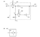
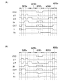
図1は、不揮発性のラッチ回路400の構成を示している。図1に示す不揮発性のラッチ
回路400は、第1の素子(D1)412の出力が第2の素子(D2)413の入力に電
気的に接続され、第2の素子(D2)413の出力が第2のトランジスタ432を介して
第1の素子(D1)412の入力に電気的に接続されるループ構造を有している。
<Configuration and operation of nonvolatile latch circuit>
FIG. 1 shows a configuration of a
第1の素子(D1)412の入力は、第1のトランジスタ431を介して入力信号が与え
られる配線414に電気的に接続されている。第1の素子(D1)412の出力は、出力
信号が与えられる配線415に電気的に接続されている。入力信号が与えられる配線41
4は、前段の回路から不揮発性のラッチ回路400へ入力される信号が与えられる配線で
ある。出力信号が与えられる配線415は、不揮発性のラッチ回路400から後段の回路
へ出力される信号が与えられる配線である。
An input of the first element (D1) 412 is electrically connected to a
第1の素子(D1)412の入力が複数ある場合は、そのうちの一を、第1のトランジス
タ431を介して入力信号が与えられる配線414に電気的に接続することができる。第
2の素子(D2)413の入力が複数ある場合は、そのうちの一を第1の素子(D1)4
12の出力に電気的に接続することができる。
In the case where there are a plurality of inputs of the first element (D1) 412, one of them can be electrically connected to the
It can be electrically connected to 12 outputs.
第1の素子(D1)412は、入力された信号を反転したものが出力となる素子を用いる
ことができる。例えば、第1の素子(D1)412には、インバータ、NAND(ナンド
)、NOR(ノア)、クロックドインバータ等を用いることができる。また、第2の素子
(D2)413は、入力された信号を反転したものが出力となる素子を用いることができ
る。例えば、第2の素子(D2)413には、インバータ、NAND(ナンド)、NOR
(ノア)、クロックドインバータ等を用いることができる。
As the first element (D1) 412, an element in which an inverted signal is output can be used. For example, for the first element (D1) 412, an inverter, NAND (NAND), NOR (NOR), a clocked inverter, or the like can be used. As the second element (D2) 413, an element in which an input signal is inverted and an output is used can be used. For example, the second element (D2) 413 includes an inverter, NAND (NAND), NOR
(Noah), a clocked inverter, or the like can be used.
上記不揮発性のラッチ回路400は、チャネル形成領域を構成する半導体材料として酸化
物半導体を用いた第1のトランジスタ431と第2のトランジスタ432をスイッチング
素子として用いている。また上記不揮発性のラッチ回路400は、この第1のトランジス
タ431と第2のトランジスタ432のソース電極又はドレイン電極にそれぞれ電気的に
接続された容量404を有している。すなわち、第1のトランジスタ431のソース電極
及びドレイン電極の一方に容量404の一方の電極が電気的に接続され、第2のトランジ
スタ432のソース電極及びドレイン電極の一方に容量404の一方の電極が電気的に接
続されている。第1のトランジスタ431のソース電極及びドレイン電極の他方は、入力
信号が与えられる配線に電気的に接続されている。第2のトランジスタ432のソース電
極及びドレイン電極の他方は、第2の素子の出力に電気的に接続されている。容量404
の他方の電極には電位Vcが与えられる。
In the
The other electrode is supplied with a potential Vc.
上記において、不揮発性のラッチ回路400が有する第1の素子412は、少なくとも第
3のトランジスタ421を有している。この第3のトランジスタ421のゲートは第1の
素子412の入力に電気的に接続されている。すなわち、第3のトランジスタ421のゲ
ートは、第2のトランジスタ432のソース電極及びドレイン電極の一方に電気的に接続
されている。また、第3のトランジスタ421のゲートは、第1のトランジスタ431の
ソース電極及びドレイン電極の一方に電気的に接続されている。
In the above, the
また、第1のトランジスタ431と第2のトランジスタ432はそれぞれ、図1に示す構
成に代えて、図2(A)又は図2(B)に示す構成とすることができる。
The
図2(A)に示すトランジスタは、第1のゲート電極と第2のゲート電極を有している。
第2のゲート電極は、チャネル形成領域を構成する酸化物半導体層を間にして第1のゲー
ト電極と反対側に設けられている。第1のゲート電極は信号が与えられる配線に電気的に
接続されている。第2のゲート電極は、所定の電位が与えられる配線に電気的に接続され
ている。例えば、第2のゲート電極は、負の電位或いは接地電位(GND)が与えられる
配線に電気的に接続されている。
The transistor illustrated in FIG. 2A includes a first gate electrode and a second gate electrode.
The second gate electrode is provided on the opposite side to the first gate electrode with an oxide semiconductor layer forming a channel formation region interposed therebetween. The first gate electrode is electrically connected to a wiring to which a signal is supplied. The second gate electrode is electrically connected to a wiring to which a predetermined potential is applied. For example, the second gate electrode is electrically connected to a wiring to which a negative potential or a ground potential (GND) is applied.
図2(A)に示すトランジスタを用いた不揮発性のラッチ回路では、図1に示す不揮発性
のラッチ回路が有する効果に加えて、トランジスタの電気的特性(例えば、しきい値電圧
)の調節が容易になるという効果が得られる。例えば、トランジスタの第2のゲート電極
に負電位を与えることで、トランジスタを容易にノーマリーオフとする(すなわち、第1
のゲート電極とソース電極間の電圧がほぼ0Vの状態においてトランジスタをオフとする
)ことができる。
In the nonvolatile latch circuit using the transistor illustrated in FIG. 2A, in addition to the effects of the nonvolatile latch circuit illustrated in FIG. 1, the electrical characteristics (eg, threshold voltage) of the transistor are adjusted. The effect that it becomes easy is acquired. For example, by applying a negative potential to the second gate electrode of the transistor, the transistor can be easily normally off (ie, the first gate electrode).
The transistor can be turned off when the voltage between the gate electrode and the source electrode is approximately 0V.
図2(B)に示すトランジスタは、第1のゲート電極と第2のゲート電極を有している。
第2のゲート電極は、チャネル形成領域を構成する酸化物半導体層を間にして第1のゲー
ト電極と反対側に設けられている。第2のゲート電極は、第1のゲート電極に電気的に接
続されている。
The transistor illustrated in FIG. 2B includes a first gate electrode and a second gate electrode.
The second gate electrode is provided on the opposite side to the first gate electrode with an oxide semiconductor layer forming a channel formation region interposed therebetween. The second gate electrode is electrically connected to the first gate electrode.
図2(B)に示すトランジスタを用いた不揮発性のラッチ回路では、図1に示す不揮発性
のラッチ回路が有する効果に加えて、トランジスタの電流量を増加できるという効果が得
られる。
In the nonvolatile latch circuit using the transistor illustrated in FIG. 2B, in addition to the effect of the nonvolatile latch circuit illustrated in FIG. 1, an effect that the current amount of the transistor can be increased is obtained.
図1又は図2に示す構成を有する不揮発性のラッチ回路は、以下のように、データの書き
込み、保持、読み出しが可能である。なお、以下では、図1の構成を元に説明するが、他
の構成の場合も同様である。
The nonvolatile latch circuit having the configuration shown in FIG. 1 or 2 can write, hold, and read data as follows. In the following, description will be made based on the configuration of FIG. 1, but the same applies to other configurations.
上で説明したとおり、不揮発性のラッチ回路400は、第1の素子(D1)412の出力
が第2の素子(D2)413の入力に電気的に接続され、第2の素子(D2)413の出
力が第2のトランジスタ432を介して第1の素子(D1)412の入力に電気的に接続
されるループ構造を有している。このループ構造の所定の位置に、容量404及び第3の
トランジスタ421のゲート容量が電気的に接続されている。具体的には、第1の素子(
D1)412の入力に、容量404の一方の電極及び第3のトランジスタ421のゲート
が電気的に接続されている。このように容量404及び第3のトランジスタ421のゲー
ト容量は、不揮発性のラッチ回路400が有するループ構造の所定の位置に電気的に接続
されている。これにより、容量404及び第3のトランジスタ421のゲート容量には、
ラッチ回路へデータを書き込む度に、データに応じた電荷が蓄積される。つまり、ラッチ
回路400が有するデータは自動的に不揮発性ラッチに書き込まれる(書き込み)。デー
タの書き換えも同様に行うことができる。
As described above, the
D1) One electrode of the
Each time data is written to the latch circuit, charges corresponding to the data are accumulated. That is, the data included in the
容量404及び第3のトランジスタ421のゲート容量に書き込まれたデータの保持、す
なわち、これらの容量に蓄積された電荷の保持は、第1のトランジスタ431と第2のト
ランジスタ432のゲートにそれぞれのトランジスタがオフとなる電位を与え、それぞれ
のトランジスタをオフすることにより行うことができる(保持)。
The data written in the gate capacitance of the
ここで、第1のトランジスタ431及び第2のトランジスタ432として、チャネル形成
領域に酸化物半導体層を用い、ノーマリーオフの特性を有し、かつオフ電流が非常に小さ
いトランジスタを用いることにより、ラッチ回路400が有する少なくとも第1の素子(
D1)412、第2の素子(D2)413の電源電圧の供給を停止した後も、容量に蓄積
された電荷をそのまま保持し続けることができる。これにより、上記電源電圧の供給を停
止した後も、ラッチ回路400の論理状態を記憶しつづけることができる。
Here, as the
D1) 412 and the second element (D2) 413 can continue to hold the charge accumulated in the capacitor even after the supply of power supply voltage is stopped. Thus, the logic state of the
容量404及び第3のトランジスタ421のゲート容量は、第1の素子(D1)412の
入力に電気的に接続されている。従って、ラッチ回路400が有する少なくとも第1の素
子(D1)412の電源電圧の供給が再び開始された後は、容量404及び第3のトラン
ジスタ421のゲート容量に蓄積された電荷に応じて、出力信号OUTの電位が決まる。
つまり、容量404及び第3のトランジスタ421のゲート容量に書き込まれたデータの
読み出しを行うことができる(読み出し)。
The
That is, data written to the
上記において、第1のトランジスタ431と第2のトランジスタ432のそれぞれのチャ
ネル形成領域を構成する酸化物半導体層として、四元系金属酸化物であるIn−Sn−G
a−Zn−Oや、三元系金属酸化物であるIn−Ga−Zn−O、In−Sn−Zn−O
、In−Al−Zn−O、Sn−Ga−Zn−O、Al−Ga−Zn−O、Sn−Al−
Zn−Oや、二元系金属酸化物であるIn−Zn−O、Sn−Zn−O、Al−Zn−O
、Zn−Mg−O、Sn−Mg−O、In−Mg−Oや、In−O、Sn−O、Zn−O
などを用いた酸化物半導体層を適用することができる。また、上記酸化物半導体材料にS
iO2を含ませても良い。
In the above, an In—Sn—G that is a quaternary metal oxide is used as an oxide semiconductor layer included in each channel formation region of the
a-Zn-O, In-Ga-Zn-O and In-Sn-Zn-O which are ternary metal oxides
In-Al-Zn-O, Sn-Ga-Zn-O, Al-Ga-Zn-O, Sn-Al-
Zn-O, binary metal oxides In-Zn-O, Sn-Zn-O, Al-Zn-O
Zn-Mg-O, Sn-Mg-O, In-Mg-O, In-O, Sn-O, Zn-O
An oxide semiconductor layer using any of the above can be used. In addition, the oxide semiconductor material includes S.
iO 2 may be included.
上記において、例えば、In−Sn−Ga−Zn−O系酸化物半導体とは、少なくともI
n、Sn、Ga、Znを含む酸化物半導体という意味であり、それぞれの金属元素の組成
比に制限はなく、また、In、Sn、Ga、Zn以外の金属元素が含まれていてもよい。
In the above, for example, an In—Sn—Ga—Zn—O-based oxide semiconductor means at least I
It means an oxide semiconductor containing n, Sn, Ga, and Zn, and there is no limitation on the composition ratio of each metal element, and a metal element other than In, Sn, Ga, and Zn may be contained.
また、酸化物半導体層として、InMO3(ZnO)m(m>0、且つ自然数でない)で
表記される材料を含む膜を用いることができる。ここで、Mは、Ga、Al、Mnおよび
Coから選ばれた一または複数の金属元素を示す。例えば、Mとしては、Ga、Gaおよ
びAl、GaおよびMn、GaおよびCoなどを適用することができる。
As the oxide semiconductor layer, a film containing a material represented by InMO 3 (ZnO) m (m> 0 is not a natural number) can be used. Here, M represents one or more metal elements selected from Ga, Al, Mn, and Co. For example, Ga, Ga and Al, Ga and Mn, Ga and Co, etc. can be applied as M.
上記において、酸化物半導体層の水素濃度は5×10¹⁹/cm3以下、望ましくは5×
1018/cm3以下、より望ましくは5×1017/cm3以下、より望ましくは1×
1016/cm3未満とすることができる。また、酸化物半導体層のキャリア濃度は1×
1014/cm3未満、望ましくは1×1012/cm3未満、より望ましくは1×10
11/cm3未満とすることができる。
In the above, the hydrogen concentration of the oxide semiconductor layer is 5 × 10 19 / cm 3 or less, preferably 5 ×
10 18 / cm 3 or less, more desirably 5 × 10 17 / cm 3 or less, more desirably 1 ×
It can be less than 10 16 / cm 3 . The carrier concentration of the oxide semiconductor layer is 1 ×
Less than 10 14 / cm 3 , desirably less than 1 × 10 12 / cm 3 , more desirably 1 × 10
It can be less than 11 / cm 3 .
上記において、酸化物半導体を用いたトランジスタ431、トランジスタ432は、ボト
ムゲート型であっても良いし、トップゲート型であっても良い。また、ボトムコンタクト
型であっても良いし、トップコンタクト型であっても良い。ボトムゲート型トランジスタ
は、少なくとも絶縁表面上のゲート電極と、ゲート電極上のゲート絶縁膜と、ゲート絶縁
膜上においてゲート電極と重なるチャネル形成領域となる酸化物半導体層とを有する。ト
ップゲート型トランジスタは、少なくとも絶縁表面上のチャネル形成領域となる酸化物半
導体層と、酸化物半導体層上のゲート絶縁膜と、ゲート絶縁膜上において酸化物半導体膜
と重なるゲート電極とを有する。ボトムコンタクト型トランジスタは、ソース電極及びド
レイン電極上にチャネル形成領域となる酸化物半導体層を有する。トップコンタクト型ト
ランジスタは、チャネル形成領域となる酸化物半導体層上にソース電極及びドレイン電極
を有する。
In the above, the
上記酸化物半導体材料により形成された酸化物半導体層をチャネル形成領域に用いたトラ
ンジスタ(第1のトランジスタ431、第2のトランジスタ432)は、例えば、チャネ
ル幅Wが1×104μmでチャネル長が3μmの素子であっても、ドレイン電極に印加す
るドレイン電圧Vdが+1V又は+10Vの場合に、ゲート電極に印加するゲート電圧V
gが−5Vから−20Vの範囲では、室温でのオフ電流が10−13A以下、サブスレッ
ショルドスイング値(S値)が0.1V/dec.程度(ゲート絶縁膜厚100nm)の
特性が得られる。また上記トランジスタは、ゲート電極とソース電極間の電圧がほぼ0V
の状態においてトランジスタがオフとなるノーマリーオフ(nチャネル型の場合、しきい
値電圧が正の値となること)の特性を有している。
A transistor using the oxide semiconductor layer formed using the oxide semiconductor material for a channel formation region (the
When g is in the range of −5 V to −20 V, the off-current at room temperature is 10 −13 A or less, and the subthreshold swing value (S value) is 0.1 V / dec. The characteristic of the extent (gate insulating
In this state, the transistor is normally off (in the n-channel type, the threshold voltage is a positive value).
従って、上記トランジスタは、ゲート電極とソース電極間の電圧がほぼ0Vの状態におけ
るオフ電流(リーク電流ともいう)が、シリコンをチャネル形成領域に用いたトランジス
タに比べて著しく小さいという特性を有している。例えば、上記のW=1×104μmの
トランジスタにおいてはチャネル幅1μmあたりに換算した室温でのリーク電流は10a
A/μm以下となる。
Therefore, the transistor has a characteristic that an off-state current (also referred to as a leakage current) in a state where the voltage between the gate electrode and the source electrode is approximately 0 V is significantly smaller than a transistor using silicon for a channel formation region. Yes. For example, in the above-mentioned transistor of W = 1 × 10 4 μm, the leakage current at room temperature converted per channel width of 1 μm is 10a
A / μm or less.
そのため、チャネル形成領域に酸化物半導体層を用いたトランジスタをスイッチング素子
として用いることで、ラッチ回路への電源電圧の供給が停止された後も、容量に蓄積され
た電荷をそのまま保持し続けることができる。すなわち、容量に書き込まれたデータをそ
のまま保持し続けることができる。
Therefore, by using a transistor including an oxide semiconductor layer for a channel formation region as a switching element, electric charge accumulated in a capacitor can be held as it is even after supply of power supply voltage to the latch circuit is stopped. it can. That is, the data written in the capacity can be held as it is.
例えば、リフレッシュタイムは、シリコンをチャネル形成領域に用いたトランジスタを用
いて構成されたDRAMよりも遙かに長時間とすることが可能であり、不揮発性メモリと
同程度のメモリ保有性(データ保持性)を有することができる。また、ラッチ回路への電
源電圧の供給が再び開始された後には、容量に保持されたデータを読み出すことができる
。これにより、電源電圧の供給の停止前の論理状態に復元することができる。
For example, the refresh time can be much longer than that of a DRAM configured using a transistor in which silicon is used for a channel formation region, and has a memory retention (data retention) similar to that of a nonvolatile memory. ). In addition, after the supply of the power supply voltage to the latch circuit is started again, data held in the capacitor can be read. Thereby, it is possible to restore the logic state before the supply of the power supply voltage is stopped.
また、上記トランジスタは温度特性も良好であり、高温でもオフ電流が十分低く、オン電
流が十分高いものを得ることができる。例えば、トランジスタのVg−Id特性は−25
℃〜150℃の範囲において、オン電流、移動度、S値の温度依存性が少ないというデー
タが得られている。また、オフ電流は上記温度範囲において、1×10⁻¹³A以下と極
めて小さいデータが得られている。
Further, the transistor has favorable temperature characteristics, and a transistor with a sufficiently low off-state current and a sufficiently high on-state current can be obtained even at high temperatures. For example, the Vg-Id characteristic of a transistor is -25.
Data indicating that the temperature dependence of the on-current, mobility, and S value is small in the range of from ° C to 150 ° C. Further, extremely small data of 1 × 10 −13 A or less is obtained in the temperature range.
上記特性は、トランジスタのチャネル形成領域に、水素濃度が十分に低減されて高純度化
され、キャリア濃度が十分に小さい、真性(i型)または実質的に真性(i型)にされた
酸化物半導体を用いることにより、得られたものと考えられる。すなわち、n型不純物で
ある水素を酸化物半導体から除去し、酸化物半導体の主成分以外の不純物が極力含まれな
いように高純度化することにより酸化物半導体を真性(i型)または実質的に真性(i型
)とした酸化物半導体を、トランジスタのチャネル形成領域に用いたものである。
The above characteristic is that an oxide which is made intrinsic (i-type) or substantially intrinsic (i-type) in which a hydrogen concentration is sufficiently reduced in a channel formation region of a transistor to be highly purified and a carrier concentration is sufficiently low. It is thought that it was obtained by using a semiconductor. In other words, n-type impurity hydrogen is removed from an oxide semiconductor, and the oxide semiconductor is intrinsic (i-type) or substantially purified by being highly purified so that impurities other than the main component of the oxide semiconductor are included as much as possible. In addition, an intrinsic (i-type) oxide semiconductor is used for a channel formation region of a transistor.
なお、本明細書では、キャリア濃度が1×10¹¹/cm3未満の半導体を「真性」ある
いは「i型」、それ以上であるが、1×10¹²/cm3未満のものを、「実質的に真性
」あるいは「実質的にi型」と呼ぶ。
In this specification, a semiconductor having a carrier concentration of less than 1 × 10 11 / cm 3 is “intrinsic” or “i-type”, and a semiconductor having a carrier concentration of less than 1 × 10 12 / cm 3 "Intrinsic" or "substantially i-type".
このような、真性(i型)、あるいは、実質的に真性(i型)の酸化物半導体を用いたト
ランジスタは、チャネル幅Wが1μmあたりのオフ電流が10aA(1×10⁻¹⁷A)
/μm以下、より好ましくは1aA(1×10−18A)/μm以下とすることができる
。
Such a transistor using an intrinsic (i-type) or substantially intrinsic (i-type) oxide semiconductor has an off current of 10 aA (1 × 10 −17 A) per channel width W of 1 μm.
/ Μm or less, more preferably 1 aA (1 × 10 −18 A) / μm or less.
このように、本実施の形態は、チャネル形成領域を構成する半導体材料として上記酸化物
半導体を用いた第1のトランジスタ431、第2のトランジスタ432をスイッチング素
子として用いることで、温度動作範囲が広く高温でも安定に動作し、電源を切っても記憶
している論理状態が消えない不揮発性のラッチ回路を提供するものである。
As described above, in this embodiment, the
なお、酸化物半導体層中の水素濃度は、二次イオン質量分析法(SIMS:Second
ary Ion Mass Spectrometry)で測定したものである。
Note that the hydrogen concentration in the oxide semiconductor layer is determined by secondary ion mass spectrometry (SIMS).
measured by ary Ion Mass Spectrometry).
<不揮発性のラッチ回路が有する素子の構成>
不揮発性のラッチ回路400が有する素子のうち、酸化物半導体を用いた第1のトランジ
スタ431と第2のトランジスタ432以外の素子は、半導体材料として酸化物半導体以
外の材料を用いることができる。酸化物半導体以外の材料としては、単結晶シリコン、結
晶性シリコンなどを用いることができる。例えば、第1のトランジスタ431と第2のト
ランジスタ432以外の素子は、半導体材料を含む基板に設けることができる。半導体材
料を含む基板としては、シリコンウェハ、SOI(Silicon on Insula
tor)基板、絶縁表面上のシリコン膜などを用いることができる。酸化物半導体以外の
材料を用いることにより、高速動作が可能となる。
<Structure of element of nonvolatile latch circuit>
Among the elements included in the
tor) A substrate, a silicon film on an insulating surface, or the like can be used. By using a material other than an oxide semiconductor, high-speed operation is possible.
例えば、第1の素子(D1)412が有する第3のトランジスタ421を、酸化物半導体
以外の材料(例えばシリコン)を用いて形成することができる。また、第1の素子(D1
)412、第2の素子(D2)413が有する他の素子についても、酸化物半導体以外の
材料(例えばシリコン)を用いて形成することができる。
For example, the
) 412 and other elements included in the second element (D2) 413 can also be formed using a material other than an oxide semiconductor (eg, silicon).
また、不揮発性のラッチ回路400が有する容量404などの素子は、酸化物半導体を用
いたトランジスタ(第1のトランジスタ431、第2のトランジスタ432)又は酸化物
半導体以外の材料(例えばシリコン)を用いたトランジスタを構成する半導体層、絶縁層
、導電層あるいは配線を構成する導電層などと同じ層に、同じ材料を用いて形成すること
ができる。
For the element such as the
例えば、下部に酸化物半導体以外の材料を用いた第3のトランジスタ421を有し、上部
に酸化物半導体を用いた第1のトランジスタ431、第2のトランジスタ432を有する
構成とすることができる。これにより、両者の特性を併せ持つ優れた不揮発性のラッチ回
路を作製することができる。
For example, the structure can include a
図3は、上記不揮発性のラッチ回路が有する素子の構成の一例を示す。図3(A)は、下
部に酸化物半導体以外の材料を用いたトランジスタ421を有し、上部に酸化物半導体を
用いたトランジスタ402を有するものである。トランジスタ402は、第1のトランジ
スタ431、第2のトランジスタ432として用いられる。トランジスタ421は、第3
のトランジスタ421として用いられる。
FIG. 3 illustrates an example of a structure of an element included in the nonvolatile latch circuit. FIG. 3A illustrates a
The
図3(A)には断面を、図3(B)には平面をそれぞれ示す。ここで、図3(A)は、図
3(B)の線A1−A2および線B1−B2における断面に相当する。図3(A)および
図3(B)は、下部に酸化物半導体以外の材料を用いたトランジスタ421を有し、上部
に酸化物半導体を用いたトランジスタ402を有するものである。
3A shows a cross section, and FIG. 3B shows a plane. Here, FIG. 3A corresponds to a cross section taken along line A1-A2 and line B1-B2 in FIG. 3A and 3B each include a
トランジスタ421は、半導体材料を含む基板100に設けられたチャネル形成領域11
6と、チャネル形成領域116を挟むように設けられた不純物領域114および高濃度不
純物領域120(これらをあわせて単に不純物領域とも呼ぶ)と、チャネル形成領域11
6上に設けられたゲート絶縁層108aと、ゲート絶縁層108a上に設けられたゲート
電極110aと、不純物領域114と電気的に接続するソース電極またはドレイン電極1
30a、および、ソース電極またはドレイン電極130bを有する(図3(A)参照)。
The
6, an
6, a
30a and a source or
ここで、ゲート電極110aの側面にはサイドウォール絶縁層118が設けられている。
また、基板100の、平面で見てサイドウォール絶縁層118と重ならない領域には、高
濃度不純物領域120を有し、高濃度不純物領域120と接する金属化合物領域124を
有する。また、基板100上にはトランジスタ421を囲むように素子分離絶縁層106
が設けられており、トランジスタ421を覆うように、層間絶縁層126および層間絶縁
層128が設けられている。なお、半導体素子が高度に微細化される場合は、サイドウォ
ール絶縁層118を有さない構成とすることもできる。
Here, a
In addition, a region of the
An interlayer insulating
ソース電極またはドレイン電極130a、ソース電極またはドレイン電極130bは、層
間絶縁層126および層間絶縁層128に形成された開口を通じて、金属化合物領域12
4と電気的に接続されている。つまり、ソース電極またはドレイン電極130a、ソース
電極またはドレイン電極130bは、金属化合物領域124を介して高濃度不純物領域1
20および不純物領域114と電気的に接続されている。
The source or
4 is electrically connected. That is, the source or
20 and the
トランジスタ402は、層間絶縁層128上に設けられたゲート電極136dと、ゲート
電極136d上に設けられたゲート絶縁層138と、ゲート絶縁層138上に設けられた
酸化物半導体層140と、酸化物半導体層140上に設けられ、酸化物半導体層140と
電気的に接続されているソース電極またはドレイン電極142a、ソース電極またはドレ
イン電極142bと、を有する(図3(A)参照)。
The
また、トランジスタ402の上には、酸化物半導体層140の一部と接するように、保護
絶縁層144が設けられており、保護絶縁層144上には層間絶縁層146が設けられて
いる。ここで、保護絶縁層144および層間絶縁層146には、ソース電極またはドレイ
ン電極142a、ソース電極またはドレイン電極142bにまで達する開口が設けられて
おり、当該開口を通じて、電極150d、電極150eが、ソース電極またはドレイン電
極142a、ソース電極またはドレイン電極142bに接して形成されている。
Further, a protective
また、電極150d、電極150eの形成と同時に、ゲート絶縁層138、保護絶縁層1
44、層間絶縁層146に設けられた開口を通じて、電極136a、電極136b、電極
136cに接する電極150a、電極150b、電極150cが形成されている。なおト
ランジスタ402としてボトムゲート型のトランジスタの例を示したが、これに限定され
ない。トップゲート型のトランジスタであっても良い。
Simultaneously with the formation of the
44. Through an opening provided in the
また、層間絶縁層146上には絶縁層152が設けられており、当該絶縁層152に埋め
込まれるように、電極154a、電極154b、電極154c、電極154dが設けられ
ている。ここで、電極154aは電極150aと接しており、電極154bは電極150
bと接しており、電極154cは電極150cおよび電極150dと接しており、電極1
54dは電極150eと接している。
An insulating
b, the
54d is in contact with the
つまり、トランジスタ402のソース電極またはドレイン電極142aは、電極130c
、電極136c、電極150c、電極154c、電極150dを介して、他の要素(酸化
物半導体以外の材料を用いたトランジスタなど)と電気的に接続されている(図3(A)
参照)。さらに、トランジスタ402のソース電極またはドレイン電極142bは、電極
150e、電極154dを介して、他の要素に電気的に接続されている。なお、接続に係
る電極(電極130c、電極136c、電極150c、電極154c、電極150d等)
の構成は、上記に限定されず、適宜追加、省略等が可能である。
That is, the source or
And electrically connected to other elements (such as a transistor using a material other than an oxide semiconductor) through the
reference). Further, the source or
The configuration is not limited to the above, and can be added or omitted as appropriate.
上記では、接続関係に係る一例を示したが、開示する発明の一態様はこれに限定されない
。
In the above, an example of connection relations is shown, but one embodiment of the disclosed invention is not limited thereto.
ここで、酸化物半導体層140は水素などの不純物が十分に除去され、高純度化されたも
のであることが望ましい。具体的には、二次イオン質量分析法(SIMS:Second
ary Ion Mass Spectrometry)で測定した酸化物半導体層14
0の水素濃度が5×10¹⁹/cm3以下、望ましくは5×1018/cm3以下、より
望ましくは5×10¹⁷/cm3以下、より望ましくは1×1016/cm3未満となる
ようにする。
Here, it is preferable that the
oxide semiconductor layer 14 measured by ary Ion Mass Spectrometry)
The hydrogen concentration of 0 is 5 × 10 19 / cm 3 or less, desirably 5 × 10 18 / cm 3 or less, more desirably 5 × 10 17 / cm 3 or less, and more desirably less than 1 × 10 16 / cm 3. Like that.
なお、水素濃度が十分に低減され、高純度化された酸化物半導体層140では、一般的な
シリコンウェハ(リンやボロンなどの不純物元素が微量に添加されたシリコンウェハ)に
おけるキャリア濃度(1×10¹⁴/cm3程度)と比較して、十分に小さいキャリア濃
度の値(例えば、1×10¹²/cm3未満、望ましくは、1×1011/cm3未満)
をとる。
Note that in the highly purified
Take.
このように、i型化または実質的にi型化された酸化物半導体を用いることで、極めて優
れたオフ電流特性のトランジスタ402を得ることができる。例えば、チャネル幅Wが1
×104μmでチャネル長が3μmの素子であっても、ドレイン電極に印加するドレイン
電圧Vdが+1V又は+10Vの場合に、ゲート電極に印加するゲート電圧Vgが−5V
から−20Vの範囲では、室温でのオフ電流は1×10⁻¹³A以下の特性を有している
。また、上記トランジスタは、ノーマリーオフのトランジスタ特性を有している。
In this manner, by using an i-type or substantially i-type oxide semiconductor, the
Even in an element having a channel length of 3 μm and × 10 4 μm, when the drain voltage Vd applied to the drain electrode is +1 V or +10 V, the gate voltage Vg applied to the gate electrode is −5 V
To −20V, the off-state current at room temperature has a characteristic of 1 × 10 −13 A or less. The transistor has normally-off transistor characteristics.
従って、ゲート電極とソース電極間の電圧がほぼ0Vの状態におけるオフ電流(リーク電
流ともいう)が、シリコンをチャネル形成領域に用いたトランジスタに比べて著しく小さ
いという特性を有している。例えば、チャネル幅1μmあたりに換算した室温でのリーク
電流は10aA/μm以下とすることができる。
Therefore, the off-state current (also referred to as leakage current) in a state where the voltage between the gate electrode and the source electrode is approximately 0 V is significantly smaller than that of a transistor using silicon for a channel formation region. For example, the leakage current at room temperature converted per channel width of 1 μm can be 10 aA / μm or less.
また、トランジスタ402は温度特性も良好であり、高温でもオフ電流が十分低く、オン
電流が十分高いものを得ることができる。例えば、トランジスタのVg−Id特性は−2
5℃〜150℃の範囲において、オン電流、移動度、S値の温度依存性が少ないというデ
ータが得られている。また、オフ電流は上記温度範囲において、1×10⁻¹³A以下と
極めて小さいデータが得られている。
In addition, the
In the range of 5 ° C. to 150 ° C., data indicating that the temperature dependence of on-current, mobility, and S value is small is obtained. Further, extremely small data of 1 × 10 −13 A or less is obtained in the temperature range.
このような、真性(i型)、あるいは、実質的に真性(i型)の酸化物半導体を用いたト
ランジスタは、チャネル幅Wが1μmあたりのオフ電流が10aA(1×10⁻¹⁷A)
/μm以下、より好ましくは1aA(1×10−18A)/μm以下とすることができる
。
Such a transistor using an intrinsic (i-type) or substantially intrinsic (i-type) oxide semiconductor has an off current of 10 aA (1 × 10 −17 A) per channel width W of 1 μm.
/ Μm or less, more preferably 1 aA (1 × 10 −18 A) / μm or less.
このように、水素濃度が十分に低減されて高純度化された酸化物半導体層140を適用し
、トランジスタ402のオフ電流を低減することにより、新たな構成の半導体装置を実現
することができる。
In this manner, by applying the highly purified
<不揮発性のラッチ回路が有する素子の作製方法>
次に、上記不揮発性のラッチ回路が有する素子の作製方法の一例について説明する。以下
では、はじめにトランジスタ421の作製方法について図4を参照して説明し、その後、
トランジスタ402の作製方法について図5または図6を参照して説明する。以下に示す
作製方法により、上記不揮発性のラッチ回路が有する素子を作製することができる。なお
、図4では、図3(A)におけるA1−A2に相当する断面のみを示す。また、図5また
は図6では、図3(A)におけるA1−A2およびB1−B2に相当する断面を示す。
<Method for Manufacturing Element of Nonvolatile Latch Circuit>
Next, an example of a method for manufacturing an element included in the nonvolatile latch circuit will be described. Hereinafter, a method for manufacturing the
A method for manufacturing the
<下部トランジスタの作製方法>
まず、半導体材料を含む基板100を用意する(図4(A)参照)。半導体材料を含む基
板100としては、シリコンや炭化シリコンなどの単結晶半導体基板、多結晶半導体基板
、シリコンゲルマニウムなどの化合物半導体基板、SOI基板などを適用することができ
る。ここでは、半導体材料を含む基板100として、単結晶シリコン基板を用いる場合の
一例について示すものとする。
<Production method of lower transistor>
First, the
なお、一般に「SOI基板」は、絶縁表面上にシリコン半導体層が設けられた構成の基板
をいうが、本明細書等においては、絶縁表面上にシリコン以外の材料からなる半導体層が
設けられた構成の基板をも含む概念として用いる。つまり、「SOI基板」が有する半導
体層は、シリコン半導体層に限定されない。また、SOI基板には、ガラス基板などの絶
縁基板上に半導体層が設けられた構成のものが含まれるものとする。
In general, an “SOI substrate” refers to a substrate having a structure in which a silicon semiconductor layer is provided on an insulating surface. In this specification and the like, a semiconductor layer made of a material other than silicon is provided on an insulating surface. It is used as a concept including the substrate of the configuration. That is, the semiconductor layer included in the “SOI substrate” is not limited to the silicon semiconductor layer. The SOI substrate includes a substrate in which a semiconductor layer is provided over an insulating substrate such as a glass substrate.
基板100上には、素子分離絶縁層を形成するためのマスクとなる保護層102を形成す
る(図4(A)参照)。保護層102としては、例えば、酸化シリコンや窒化シリコン、
窒化酸化シリコンなどを材料とする絶縁層を用いることができる。なお、この工程の前後
において、トランジスタのしきい値電圧を制御するために、n型の導電性を付与する不純
物元素やp型の導電性を付与する不純物元素を基板100に添加してもよい。半導体がシ
リコンの場合、n型の導電性を付与する不純物としては、例えば、リンや砒素などを用い
ることができる。また、p型の導電性を付与する不純物としては、例えば、硼素、アルミ
ニウム、ガリウムなどを用いることができる。
A
An insulating layer formed using silicon nitride oxide or the like can be used. Note that an impurity element imparting n-type conductivity or an impurity element imparting p-type conductivity may be added to the
次に、上記の保護層102をマスクとしてエッチングを行い、保護層102に覆われてい
ない領域(露出している領域)の基板100の一部を除去する。これにより分離された半
導体領域104が形成される(図4(B)参照)。当該エッチングには、ドライエッチン
グを用いるのが好適であるが、ウェットエッチングを用いても良い。エッチングガスやエ
ッチング液は、被エッチング材料に応じて適宜選択することができる。
Next, etching is performed using the
次に、半導体領域104を覆うように絶縁層を形成し、半導体領域104に重畳する領域
の絶縁層を選択的に除去することで、素子分離絶縁層106を形成する(図4(B)参照
)。当該絶縁層は、酸化シリコンや窒化シリコン、窒化酸化シリコンなどを用いて形成さ
れる。絶縁層の除去方法としては、CMPなどの研磨処理やエッチング処理などがあるが
、そのいずれを用いても良い。なお、半導体領域104の形成後、または、素子分離絶縁
層106の形成後には、上記保護層102を除去する。
Next, an insulating layer is formed so as to cover the
次に、半導体領域104上に絶縁層を形成し、当該絶縁層上に導電材料を含む層を形成す
る。
Next, an insulating layer is formed over the
絶縁層は後のゲート絶縁層となるものであり、CVD法やスパッタリング法等を用いて得
られる酸化シリコン、窒化酸化シリコン、窒化シリコン、酸化ハフニウム、酸化アルミニ
ウム、酸化タンタル等を含む膜の単層構造または積層構造とすると良い。他に、高密度プ
ラズマ処理や熱酸化処理によって、半導体領域104の表面を酸化、窒化することにより
、上記絶縁層を形成してもよい。高密度プラズマ処理は、例えば、He、Ar、Kr、X
eなどの希ガス、酸素、酸化窒素、アンモニア、窒素、水素などの混合ガスを用いて行う
ことができる。また、絶縁層の厚さは特に限定されないが、例えば、1nm以上100n
m以下とすることができる。
The insulating layer will be a gate insulating layer later, and is a single layer of a film containing silicon oxide, silicon nitride oxide, silicon nitride, hafnium oxide, aluminum oxide, tantalum oxide, or the like obtained by using a CVD method or a sputtering method. A structure or a stacked structure is preferable. In addition, the insulating layer may be formed by oxidizing and nitriding the surface of the
This can be performed using a rare gas such as e, or a mixed gas of oxygen, nitrogen oxide, ammonia, nitrogen, hydrogen, or the like. Further, the thickness of the insulating layer is not particularly limited, but for example, 1 nm or more and 100 n
m or less.
導電材料を含む層は、アルミニウムや銅、チタン、タンタル、タングステン等の金属材料
を用いて形成することができる。また、導電性を付与する不純物元素を含む多結晶シリコ
ンなどの半導体材料を用いて、導電材料を含む層を形成しても良い。形成方法も特に限定
されず、蒸着法、CVD法、スパッタリング法、スピンコート法などの各種成膜方法を用
いることができる。なお、本実施の形態では、導電材料を含む層を、金属材料を用いて形
成する場合の一例について示すものとする。
The layer including a conductive material can be formed using a metal material such as aluminum, copper, titanium, tantalum, or tungsten. Alternatively, the layer including a conductive material may be formed using a semiconductor material such as polycrystalline silicon containing an impurity element imparting conductivity. There is no particular limitation on the formation method, and various film formation methods such as an evaporation method, a CVD method, a sputtering method, and a spin coating method can be used. Note that in this embodiment, an example of the case where the layer including a conductive material is formed using a metal material is described.
その後、上記絶縁層および導電材料を含む層を選択的にエッチングして、ゲート絶縁層1
08a、ゲート電極110aを形成する(図4(C)参照)。
Thereafter, the
08a and a
次に、ゲート電極110aを覆う絶縁層112を形成する(図4(C)参照)。そして、
半導体領域104にリン(P)又はヒ素(As)などを添加して、接合深さの浅い不純物
領域114を形成する(図4(C)参照)。なお、ここではn型トランジスタを形成する
ためにリンやヒ素を添加しているが、p型トランジスタを形成する場合には、硼素(B)
やアルミニウム(Al)などの不純物元素を添加すればよい。
Next, the insulating
An
Or an impurity element such as aluminum (Al) may be added.
なお、不純物領域114の形成により、半導体領域104のゲート絶縁層108a下部に
は、チャネル形成領域116が形成される(図4(C)参照)。ここで、添加する不純物
の濃度は適宜設定することができるが、半導体素子が高度に微細化される場合には、その
濃度を高くすることが望ましい。また、ここでは、絶縁層112を形成した後に不純物領
域114を形成する工程を採用しているが、不純物領域114を形成した後に絶縁層11
2を形成する工程としても良い。
Note that with the formation of the
2 may be formed.
次に、サイドウォール絶縁層118を形成する(図4(D)参照)。サイドウォール絶縁
層118は、絶縁層112を覆うように絶縁層を形成した後に、当該絶縁層に異方性の高
いエッチング処理を適用することで、自己整合的に形成することができる。また、この際
に、絶縁層112を部分的にエッチングして、ゲート電極110aの上面と、不純物領域
114の上面を露出させると良い。なお、半導体素子が高度に微細化される場合は、サイ
ドウォール絶縁層118を有さない構成とすることもできる。
Next, a
次に、ゲート電極110a、不純物領域114、サイドウォール絶縁層118等を覆うよ
うに、絶縁層を形成する。そして、不純物領域114と接する領域に、リン(P)やヒ素
(As)などを添加して、高濃度不純物領域120を形成する。その後、上記絶縁層を除
去し、ゲート電極110a、サイドウォール絶縁層118、高濃度不純物領域120等を
覆うように金属層122を形成する(図4(E)参照)。
Next, an insulating layer is formed so as to cover the
当該金属層122は、真空蒸着法やスパッタリング法、スピンコート法などの各種成膜方
法を用いて形成することができる。金属層122は、半導体領域104を構成する半導体
材料と反応して低抵抗な金属化合物となる金属材料を用いて形成することが望ましい。こ
のような金属材料としては、例えば、チタン、タンタル、タングステン、ニッケル、コバ
ルト、白金等がある。
The
次に、熱処理を施して、上記金属層122と半導体材料とを反応させる。これにより、高
濃度不純物領域120に接する金属化合物領域124が形成される(図4(F)参照)。
なお、ゲート電極110aとして多結晶シリコンなどを用いる場合には、ゲート電極11
0aの金属層122と接触する部分にも、金属化合物領域が形成されることになる。
Next, heat treatment is performed to react the
In the case where polycrystalline silicon or the like is used as the
A metal compound region is also formed in the portion in contact with the
上記熱処理としては、例えば、フラッシュランプの照射による熱処理を用いることができ
る。もちろん、その他の熱処理方法を用いても良いが、金属化合物の形成に係る化学反応
の制御性を向上させるためには、ごく短時間の熱処理が実現できる方法を用いることが望
ましい。なお、上記の金属化合物領域は、金属材料と半導体材料との反応により形成され
るものであり、十分に導電性が高められた領域である。当該金属化合物領域を形成するこ
とで、電気抵抗を十分に低減し、素子特性を向上させることができる。なお、金属化合物
領域124を形成した後には、金属層122は除去する。
As the heat treatment, for example, heat treatment by flash lamp irradiation can be used. Of course, other heat treatment methods may be used, but in order to improve the controllability of the chemical reaction related to the formation of the metal compound, it is desirable to use a method capable of realizing a heat treatment for a very short time. Note that the metal compound region is formed by a reaction between a metal material and a semiconductor material, and is a region in which conductivity is sufficiently increased. By forming the metal compound region, the electrical resistance can be sufficiently reduced and the device characteristics can be improved. Note that the
次に、上述の工程により形成された各構成を覆うように、層間絶縁層126、層間絶縁層
128を形成する(図4(G)参照)。層間絶縁層126や層間絶縁層128は、酸化シ
リコン、窒化酸化シリコン、窒化シリコン、酸化ハフニウム、酸化アルミニウム、酸化タ
ンタル等の無機絶縁材料を含む材料を用いて形成することができる。また、ポリイミド、
アクリル等の有機絶縁材料を用いて形成することも可能である。なお、ここでは、層間絶
縁層126と層間絶縁層128の二層構造としているが、層間絶縁層の構成はこれに限定
されない。層間絶縁層128の形成後には、その表面を、CMPやエッチング処理などに
よって平坦化しておくことが望ましい。
Next, an
It can also be formed using an organic insulating material such as acrylic. Note that although a two-layer structure of the interlayer insulating
その後、上記層間絶縁層に、金属化合物領域124にまで達する開口を形成し、当該開口
に、ソース電極またはドレイン電極130a、ソース電極またはドレイン電極130bを
形成する(図4(H)参照)。ソース電極またはドレイン電極130aやソース電極また
はドレイン電極130bは、例えば、開口を含む領域にPVD法やCVD法などを用いて
導電層を形成した後、エッチング処理やCMPといった方法を用いて、上記導電層の一部
を除去することにより形成することができる。
After that, an opening reaching the
なお、上記導電層の一部を除去してソース電極またはドレイン電極130aやソース電極
またはドレイン電極130bを形成する際には、その表面が平坦になるように加工するこ
とが望ましい。例えば、開口を含む領域にチタン膜や窒化チタン膜を薄く形成した後に、
開口に埋め込むようにタングステン膜を形成する場合には、その後のCMPによって、不
要なタングステン、チタン、窒化チタンなどを除去すると共に、その表面の平坦性を向上
させることができる。このように、ソース電極またはドレイン電極130a、ソース電極
またはドレイン電極130bを含む表面を平坦化することにより、後の工程において、良
好な電極、配線、絶縁層、半導体層などを形成することが可能となる。
Note that when the source or
When a tungsten film is formed so as to be embedded in the opening, unnecessary tungsten, titanium, titanium nitride, or the like can be removed and the flatness of the surface can be improved by subsequent CMP. In this manner, by planarizing the surface including the source or
ソース電極またはドレイン電極130a、ソース電極またはドレイン電極130bとして
用いることができる材料について特に限定はなく、各種導電材料を用いることができる。
例えば、モリブデン、チタン、クロム、タンタル、タングステン、アルミニウム、銅、ネ
オジム、スカンジウムなどの導電性材料を用いることができる。また、ここでは、金属化
合物領域124と接触するソース電極またはドレイン電極130aやソース電極またはド
レイン電極130bのみを示しているが、この工程において、図3における電極130c
などをあわせて形成することができる。
There is no particular limitation on a material that can be used for the source or
For example, a conductive material such as molybdenum, titanium, chromium, tantalum, tungsten, aluminum, copper, neodymium, or scandium can be used. Although only the source or
Etc. can be formed together.
具体的には、例えば、開口を含む領域にPVD法によりチタン膜を薄く形成し、CVD法
により窒化チタン膜を薄く形成した後に、開口に埋め込むようにタングステン膜を形成す
る方法を適用することができる。ここで、PVD法により形成されるチタン膜は、金属化
合物領域の表面に形成されうる酸化膜を還元し、金属化合物領域との接触抵抗を低減させ
る機能を有する。また、その後に形成される窒化チタン膜は、導電性材料の拡散を抑制す
るバリア機能を備える。また、チタンや窒化チタンなどによるバリア膜を形成した後に、
メッキ法により銅膜を形成してもよい。なお、いわゆるシングルダマシン法に限らず、デ
ュアルダマシン法を適用してもよい。
Specifically, for example, a method in which a titanium film is thinly formed in a region including an opening by a PVD method, a titanium nitride film is thinly formed by a CVD method, and then a tungsten film is formed so as to be embedded in the opening is applied. it can. Here, the titanium film formed by the PVD method has a function of reducing an oxide film that can be formed on the surface of the metal compound region and reducing contact resistance with the metal compound region. The titanium nitride film formed thereafter has a barrier function that suppresses diffusion of the conductive material. In addition, after forming a barrier film such as titanium or titanium nitride,
A copper film may be formed by a plating method. The dual damascene method may be applied instead of the so-called single damascene method.
以上により、半導体材料を含む基板100を用いたトランジスタ421が形成される。な
お、上記工程の後には、さらに電極や配線、絶縁層などを形成しても良い。配線の構造と
して、層間絶縁層および導電層の積層構造でなる多層配線構造を採用することにより、高
度に集積化した半導体装置を提供することができる。
Through the above steps, the
<上部トランジスタの作製方法>
次に、図5および図6を用いて、層間絶縁層128上にトランジスタ402を作製する工
程について説明する。なお、図5および図6は、層間絶縁層128上の各種電極や、トラ
ンジスタ402などの作製工程を示すものであるから、トランジスタ402の下部に存在
するトランジスタ421等については省略している。
<Method for manufacturing upper transistor>
Next, a process for manufacturing the
まず、層間絶縁層128、ソース電極またはドレイン電極130a、ソース電極またはド
レイン電極130b、電極130c上に絶縁層132を形成する(図5(A)参照)。そ
して、絶縁層132に対し、ソース電極またはドレイン電極130a、ソース電極または
ドレイン電極130b、および、電極130cにまで達する開口を形成する。そして、当
該開口に埋め込むように導電層134を形成する(図5(B)参照)。その後、エッチン
グ処理やCMPといった方法を用いて上記導電層134の一部を除去し、絶縁層132を
露出させて、電極136a、電極136b、電極136c、ゲート電極136dを形成す
る(図5(C)参照)。
First, the insulating
絶縁層132はPVD法やCVD法などを用いて形成することができる。また、酸化シリ
コン、窒化酸化シリコン、窒化シリコン、酸化ハフニウム、酸化アルミニウム、酸化タン
タル等の無機絶縁材料を含む材料を用いて形成することができる。
The insulating
絶縁層132の開口は、マスクを用いたエッチングなどの方法で形成することができる。
当該マスクは、フォトマスクを用いた露光などの方法によって形成することが可能である
。エッチングとしてはウェットエッチング、ドライエッチングのいずれを用いても良いが
、微細加工の観点からは、ドライエッチングを用いることが好適である。
The opening of the insulating
The mask can be formed by a method such as exposure using a photomask. As the etching, either wet etching or dry etching may be used. From the viewpoint of fine processing, it is preferable to use dry etching.
導電層134の形成は、PVD法やCVD法などの成膜法を用いて行うことができる。導
電層の形成に用いることができる材料としては、モリブデン、チタン、クロム、タンタル
、タングステン、アルミニウム、銅、ネオジム、スカンジウムなどの導電性材料や、これ
らの合金、化合物(例えば窒化物)などが挙げられる(図5(B)参照)。
The
より具体的には、例えば、開口を含む領域にPVD法によりチタン膜を薄く形成し、CV
D法により窒化チタン膜を薄く形成した後に、開口に埋め込むようにタングステン膜を形
成する方法を適用することができる。ここで、PVD法により形成されるチタン膜は、下
部電極(ここではソース電極またはドレイン電極130a、ソース電極またはドレイン電
極130b、電極130cなど)の表面に形成されうる酸化膜を還元し、下部電極との接
触抵抗を低減させる機能を有する。
More specifically, for example, a thin titanium film is formed by PVD in a region including the opening, and CV
A method of forming a tungsten film so as to be embedded in the opening after forming a thin titanium nitride film by the D method can be applied. Here, the titanium film formed by the PVD method reduces the oxide film that can be formed on the surface of the lower electrode (here, the source or
また、その後に形成される窒化チタン膜は、導電性材料の拡散を抑制するバリア機能を備
える。また、チタンや窒化チタンなどによるバリア膜を形成した後に、メッキ法により銅
膜を形成してもよい。なお、いわゆるシングルダマシン法に限らず、デュアルダマシン法
などを適用してもよい。
The titanium nitride film formed thereafter has a barrier function that suppresses diffusion of the conductive material. Further, after forming a barrier film made of titanium, titanium nitride, or the like, a copper film may be formed by a plating method. Note that the present invention is not limited to the so-called single damascene method, and a dual damascene method or the like may be applied.
導電層134を形成した後には、エッチング処理やCMPといった方法を用いて導電層1
34の一部を除去し、絶縁層132を露出させて、電極136a、電極136b、電極1
36c、ゲート電極136dを形成することができる(図5(C)参照)。なお、上記導
電層134の一部を除去して電極136a、電極136b、電極136c、ゲート電極1
36dを形成する際には、表面が平坦になるように加工することが望ましい。このように
、絶縁層132、電極136a、電極136b、電極136c、ゲート電極136dの表
面を平坦化することにより、後の工程において、良好な電極、配線、絶縁層、半導体層な
どを形成することが可能となる。
After the
34 is removed, the insulating
36c and a
When forming 36d, it is desirable to process so that the surface may become flat. In this manner, by planarizing the surfaces of the insulating
次に、絶縁層132、電極136a、電極136b、電極136c、ゲート電極136d
を覆うように、ゲート絶縁層138を形成する(図5(D)参照)。ゲート絶縁層138
は、CVD法やスパッタリング法等を用いて形成することができる。また、ゲート絶縁層
138は、酸化珪素、窒化珪素、酸化窒化珪素、窒化酸化珪素、酸化アルミニウム、酸化
ハフニウム、酸化タンタルなどを含むように形成するのが好適である。なお、ゲート絶縁
層138は、単層構造としても良いし、積層構造としても良い。
Next, the insulating
A
Can be formed using a CVD method, a sputtering method, or the like. The
例えば、原料ガスとして、シラン(SiH4)、酸素、窒素を用いたプラズマCVD法に
より、酸化窒化珪素でなるゲート絶縁層138を形成することができる。ゲート絶縁層1
38の厚さは特に限定されないが、例えば、10nm以上500nm以下とすることがで
きる。積層構造の場合は、例えば、膜厚50nm以上200nm以下の第1のゲート絶縁
層と、第1のゲート絶縁層上の膜厚5nm以上300nm以下の第2のゲート絶縁層の積
層とすると好適である。
For example, the
Although the thickness of 38 is not specifically limited, For example, it is 10 nm or more and 500 nm or less. In the case of a stacked structure, for example, it is preferable to stack a first gate insulating layer with a thickness of 50 nm to 200 nm and a second gate insulating layer with a thickness of 5 nm to 300 nm on the first gate insulating layer. is there.
なお、ゲート絶縁層138に水素や水などが含まれると、水素の酸化物半導体層への侵入
や、水素による酸化物半導体層中の酸素の引き抜きなどが生じ、トランジスタの特性が悪
化するおそれがある。よって、ゲート絶縁層138は、できるだけ水素や水を含まないよ
うに形成することが望ましい。
Note that when the
例えば、スパッタリング法などを用いる場合には、処理室内の残留水分を除去した状態で
ゲート絶縁層138を形成することが望ましい。また、処理室内の残留水分を除去するた
めには、クライオポンプ、イオンポンプ、チタンサブリメーションポンプなどの、吸着型
の真空ポンプを用いることが望ましい。ターボポンプにコールドトラップを加えたものを
用いてもよい。クライオポンプなどを用いて排気した処理室は、水素や水などが十分に除
去されているため、ゲート絶縁層138に含まれる不純物の濃度を低減することができる
。
For example, in the case of using a sputtering method or the like, it is preferable to form the
また、ゲート絶縁層138を形成する際には、水素や水などの不純物が、1ppm以下(
望ましくは1ppb以下)にまで低減された高純度ガスを用いることが望ましい。
Further, when the
It is desirable to use a high purity gas reduced to 1 ppb or less.
なお、不純物を除去することによりi型化または実質的にi型化された酸化物半導体(高
純度化された酸化物半導体)は、界面準位や界面電荷に対して極めて敏感であるため、こ
のような酸化物半導体を酸化物半導体層に用いる場合には、ゲート絶縁層との界面の特性
が重要である。つまり、高純度化された酸化物半導体層に接するゲート絶縁層138には
、高品質化が要求されることになる。
Note that an i-type or substantially i-type oxide semiconductor (a highly purified oxide semiconductor) by removing impurities is extremely sensitive to interface states and interface charges. In the case where such an oxide semiconductor is used for the oxide semiconductor layer, the characteristics of the interface with the gate insulating layer are important. That is, the
例えば、μ波(周波数2.45GHz)を用いた高密度プラズマCVD法は、緻密で絶縁
耐圧の高い高品質なゲート絶縁層138を形成できる点で好適である。高純度化された酸
化物半導体層と高品質ゲート絶縁層とが密接することにより、界面準位を低減して界面特
性を良好なものとすることができるからである。
For example, a high-density plasma CVD method using a μ wave (frequency: 2.45 GHz) is preferable in that a high-quality
もちろん、ゲート絶縁層として良質な絶縁層を形成できるものであれば、高純度化された
酸化物半導体層を用いる場合であっても、スパッタリング法やプラズマCVD法など他の
方法を適用することができる。また、形成後の熱処理によって、膜質や界面特性が改質さ
れる絶縁層を適用しても良い。いずれにしても、ゲート絶縁層138としての膜質が良好
であると共に、酸化物半導体層との界面準位密度を低減し、良好な界面を形成できるもの
を形成すれば良い。
Of course, as long as a high-quality insulating layer can be formed as the gate insulating layer, another method such as a sputtering method or a plasma CVD method can be applied even when a highly purified oxide semiconductor layer is used. it can. Alternatively, an insulating layer whose film quality and interface characteristics are modified by heat treatment after formation may be used. In any case, a film which has favorable film quality as the
次いで、ゲート絶縁層138上に、酸化物半導体層を形成し、マスクを用いたエッチング
などの方法によって該酸化物半導体層を加工して、島状の酸化物半導体層140を形成す
る(図5(E)参照)。
Next, an oxide semiconductor layer is formed over the
上記酸化物半導体層としては、四元系金属酸化物であるIn−Sn−Ga−Zn−O系や
、三元系金属酸化物であるIn−Ga−Zn−O系、In−Sn−Zn−O系、In−A
l−Zn−O系、Sn−Ga−Zn−O系、Al−Ga−Zn−O系、Sn−Al−Zn
−O系や、二元系金属酸化物であるIn−Zn−O系、Sn−Zn−O系、Al−Zn−
O系、Zn−Mg−O系、Sn−Mg−O系、In−Mg−O系や、In−O系、Sn−
O系、Zn−O系などの酸化物半導体を用いて形成することができる。また、上記酸化物
半導体にSiO2を含ませたものを用いても良い。
Examples of the oxide semiconductor layer include an In—Sn—Ga—Zn—O-based quaternary metal oxide, an In—Ga—Zn—O-based ternary metal oxide, and In—Sn—Zn. -O system, In-A
l-Zn-O, Sn-Ga-Zn-O, Al-Ga-Zn-O, Sn-Al-Zn
-O-based, binary metal oxides In-Zn-O-based, Sn-Zn-O-based, Al-Zn-
O, Zn—Mg—O, Sn—Mg—O, In—Mg—O, In—O, Sn—
It can be formed using an oxide semiconductor such as an O-based compound or a Zn-O-based compound. Alternatively, the oxide semiconductor containing SiO 2 may be used.
また、酸化物半導体層として、InMO3(ZnO)m(m>0、且つ自然数でない)で
表記される材料を含む薄膜を用いることができる。ここで、Mは、Ga、Al、Mnおよ
びCoから選ばれた一または複数の金属元素を示す。例えば、Mとしては、Ga、Gaお
よびAl、GaおよびMn、GaおよびCoなどを適用することができる。
As the oxide semiconductor layer, a thin film including a material represented by InMO 3 (ZnO) m (m> 0 and not a natural number) can be used. Here, M represents one or more metal elements selected from Ga, Al, Mn, and Co. For example, Ga, Ga and Al, Ga and Mn, Ga and Co, etc. can be applied as M.
本実施の形態では、酸化物半導体層としてIn−Ga−Zn−O系の金属酸化物ターゲッ
トを用いて、非晶質の酸化物半導体層をスパッタ法により形成することとする。なお、非
晶質の酸化物半導体層中にシリコンを添加することで、その結晶化を抑制することができ
るから、例えば、SiO2を2重量%以上10重量%以下含むターゲットを用いて酸化物
半導体層を形成しても良い。
In this embodiment, an amorphous oxide semiconductor layer is formed by a sputtering method using an In—Ga—Zn—O-based metal oxide target as the oxide semiconductor layer. Note that crystallization can be suppressed by adding silicon to the amorphous oxide semiconductor layer. Therefore, for example, an oxide using a target containing 2 wt% or more and 10 wt% or less of SiO 2 can be used. A semiconductor layer may be formed.
酸化物半導体層をスパッタリング法で作製するためのターゲットとしては、例えば、組成
比として、In2O3:Ga2O3:ZnO=1:1:1[mol比]などを用いること
ができる。その他に、In2O3:Ga2O3:ZnO=1:1:2[mol比]、また
はIn2O3:Ga2O3:ZnO=1:1:4[mol比]の組成比を有するターゲッ
トなどを用いても良い。金属酸化物ターゲットの充填率は90%以上100%以下、好ま
しくは95%以上(例えば99.9%)である。充填率の高い金属酸化物ターゲットを用
いることにより、緻密な酸化物半導体層が形成される。
As a target for forming the oxide semiconductor layer by a sputtering method, for example, In 2 O 3 : Ga 2 O 3 : ZnO = 1: 1: 1 [molar ratio] or the like can be used as a composition ratio. In addition, a composition ratio of In 2 O 3 : Ga 2 O 3 : ZnO = 1: 1: 2 [mol ratio] or In 2 O 3 : Ga 2 O 3 : ZnO = 1: 1: 4 [mol ratio]. You may use the target etc. which have. The filling rate of the metal oxide target is 90% or more and 100% or less, preferably 95% or more (for example, 99.9%). By using a metal oxide target with a high filling rate, a dense oxide semiconductor layer is formed.
酸化物半導体層の形成雰囲気は、希ガス(代表的にはアルゴン)雰囲気、酸素雰囲気、ま
たは、希ガス(代表的にはアルゴン)と酸素との混合雰囲気とするのが好適である。具体
的には、例えば、水素、水、水酸基、水素化物などの不純物が、1ppm以下(望ましく
は1ppb以下)にまで除去された高純度ガスを用いるのが好適である。
The atmosphere for forming the oxide semiconductor layer is preferably a rare gas (typically argon) atmosphere, an oxygen atmosphere, or a mixed atmosphere of a rare gas (typically argon) and oxygen. Specifically, for example, it is preferable to use a high-purity gas from which impurities such as hydrogen, water, hydroxyl group, and hydride are removed to 1 ppm or less (preferably 1 ppb or less).
酸化物半導体層の形成の際には、減圧状態に保持された処理室内に基板を保持し、基板温
度を100℃以上600℃以下好ましくは200℃以上400℃以下とする。基板を加熱
しながら酸化物半導体層を形成することにより、酸化物半導体層に含まれる不純物濃度を
低減することができる。また、スパッタリングによる損傷が軽減される。そして、処理室
内の残留水分を除去しつつ水素および水が除去されたスパッタガスを導入し、金属酸化物
をターゲットとして酸化物半導体層を形成する。
When forming the oxide semiconductor layer, the substrate is held in a treatment chamber kept under reduced pressure, and the substrate temperature is set to 100 ° C. to 600 ° C., preferably 200 ° C. to 400 ° C. By forming the oxide semiconductor layer while heating the substrate, the concentration of impurities contained in the oxide semiconductor layer can be reduced. Further, damage due to sputtering is reduced. Then, a sputtering gas from which hydrogen and water are removed is introduced while moisture remaining in the treatment chamber is removed, and an oxide semiconductor layer is formed using a metal oxide as a target.
処理室内の残留水分を除去するためには、吸着型の真空ポンプを用いることが好ましい。
例えば、クライオポンプ、イオンポンプ、チタンサブリメーションポンプを用いることが
できる。また、排気手段としては、ターボポンプにコールドトラップを加えたものであっ
てもよい。クライオポンプを用いて排気した成膜室においては、例えば、水素原子、水(
H2O)など水素原子を含む化合物(より好ましくは炭素原子を含む化合物も)等が排気
されるため、当該成膜室で形成した酸化物半導体層に含まれる不純物の濃度を低減できる
。
In order to remove moisture remaining in the treatment chamber, an adsorption-type vacuum pump is preferably used.
For example, a cryopump, an ion pump, or a titanium sublimation pump can be used. The exhaust means may be a turbo pump provided with a cold trap. In a film formation chamber evacuated using a cryopump, for example, hydrogen atoms, water (
Since a compound containing hydrogen atoms (more preferably a compound containing carbon atoms) or the like such as H 2 O) is exhausted, the concentration of impurities contained in the oxide semiconductor layer formed in the deposition chamber can be reduced.
形成条件としては、例えば、基板とターゲットの間との距離が100mm、圧力が0.6
Pa、直流(DC)電力が0.5kW、雰囲気が酸素(酸素流量比率100%)雰囲気、
といった条件を適用することができる。なお、パルス直流(DC)電源を用いると、ごみ
が軽減でき、膜厚分布も均一となるため、好ましい。酸化物半導体層の厚さは、2nm以
上200nm以下、好ましくは5nm以上30nm以下とする。なお、適用する酸化物半
導体材料により適切な厚さは異なるから、その厚さは用いる材料に応じて適宜選択すれば
よい。例えば、チャネル長が短い場合は、酸化物半導体層の厚さは5nm以上30nm以
下とすることができる。このように素子のサイズを小さくすることにより高集積化が図れ
るとともに、酸化物半導体層を薄くすることで短チャネル効果を抑制することができる。
As the formation conditions, for example, the distance between the substrate and the target is 100 mm, and the pressure is 0.6.
Pa, direct current (DC) power is 0.5 kW, atmosphere is oxygen (
These conditions can be applied. Note that a pulse direct current (DC) power source is preferable because dust can be reduced and the film thickness can be uniform. The thickness of the oxide semiconductor layer is 2 nm to 200 nm, preferably 5 nm to 30 nm. Note that an appropriate thickness varies depending on an oxide semiconductor material to be used, and the thickness may be selected as appropriate depending on a material to be used. For example, when the channel length is short, the thickness of the oxide semiconductor layer can be greater than or equal to 5 nm and less than or equal to 30 nm. Thus, high integration can be achieved by reducing the size of the element, and the short channel effect can be suppressed by reducing the thickness of the oxide semiconductor layer.
なお、酸化物半導体層をスパッタ法により形成する前には、アルゴンガスを導入してプラ
ズマを発生させる逆スパッタを行い、ゲート絶縁層138の表面に付着しているゴミを除
去するのが好適である。ここで、逆スパッタとは、通常のスパッタにおいては、スパッタ
ターゲットにイオンを衝突させるところ、逆に、処理表面にイオンを衝突させることによ
ってその表面を改質する方法のことをいう。処理表面にイオンを衝突させる方法としては
、アルゴン雰囲気下で処理表面側に高周波電圧を印加して、基板付近にプラズマを生成す
る方法などがある。なお、アルゴン雰囲気に代えて窒素、ヘリウム、酸素などを用いても
良い。
Note that before the oxide semiconductor layer is formed by a sputtering method, it is preferable to perform reverse sputtering in which argon gas is introduced to generate plasma to remove dust attached to the surface of the
上記酸化物半導体層のエッチングには、ドライエッチング、ウェットエッチングのいずれ
を用いても良い。もちろん、両方を組み合わせて用いることもできる。所望の形状にエッ
チングできるよう、材料に合わせてエッチング条件(エッチングガスやエッチング液、エ
ッチング時間、温度等)を適宜設定する。
For the etching of the oxide semiconductor layer, either dry etching or wet etching may be used. Of course, both can be used in combination. Etching conditions (such as an etching gas, an etchant, etching time, and temperature) are appropriately set depending on the material so that the film can be etched into a desired shape.
ドライエッチングに用いるエッチングガスには、例えば、塩素を含むガス(塩素系ガス、
例えば塩素(Cl2)、三塩化硼素(BCl3)、四塩化珪素(SiCl4)、四塩化炭
素(CCl4)など)などがある。また、フッ素を含むガス(フッ素系ガス、例えば四弗
化炭素(CF4)、六弗化硫黄(SF6)、三弗化窒素(NF3)、トリフルオロメタン
(CHF3)など)、臭化水素(HBr)、酸素(O2)、これらのガスにヘリウム(H
e)やアルゴン(Ar)などの希ガスを添加したガス、などを用いても良い。
As an etching gas used for dry etching, for example, a gas containing chlorine (chlorine-based gas,
Examples include chlorine (Cl 2 ), boron trichloride (BCl 3 ), silicon tetrachloride (SiCl 4 ), carbon tetrachloride (CCl 4 ), and the like. Gas containing fluorine (fluorine-based gas such as carbon tetrafluoride (CF 4 ), sulfur hexafluoride (SF 6 ), nitrogen trifluoride (NF 3 ), trifluoromethane (CHF 3 ), etc.), bromide Hydrogen (HBr), oxygen (O 2 ), and these gases include helium (H
e) or a gas to which a rare gas such as argon (Ar) is added may be used.
ドライエッチング法としては、平行平板型RIE(Reactive Ion Etch
ing)法や、ICP(Inductively Coupled Plasma:誘導
結合型プラズマ)エッチング法を用いることができる。所望の形状にエッチングできるよ
うに、エッチング条件(コイル型の電極に印加される電力量、基板側の電極に印加される
電力量、基板側の電極温度等)は適宜設定する。
As a dry etching method, parallel plate RIE (Reactive Ion Etch) is used.
ing) method or ICP (Inductively Coupled Plasma) etching method can be used. Etching conditions (such as the amount of power applied to the coil-type electrode, the amount of power applied to the electrode on the substrate side, and the electrode temperature on the substrate side) are set as appropriate so that the film can be etched into a desired shape.
ウェットエッチングに用いるエッチング液としては、燐酸と酢酸と硝酸を混ぜた溶液、ア
ンモニア過水(アンモニア、水、過酸化水素水の混合液)などを用いることができる。ま
た、ITO07N(関東化学社製)などのエッチング液を用いてもよい。
As an etchant used for wet etching, a mixed solution of phosphoric acid, acetic acid, and nitric acid, ammonia perwater (a mixed solution of ammonia, water, hydrogen peroxide solution), or the like can be used. An etching solution such as ITO07N (manufactured by Kanto Chemical Co., Inc.) may be used.
次いで、酸化物半導体層に第1の熱処理を行うことが望ましい。この第1の熱処理によっ
て酸化物半導体層の脱水化または脱水素化を行うことができる。第1の熱処理の温度は、
300℃以上800℃以下、好ましくは400℃以上700℃以下、より好ましくは45
0℃以上700℃以下、より好ましくは550℃以上700℃以下とすることができる。
Next, first heat treatment is preferably performed on the oxide semiconductor layer. By the first heat treatment, the oxide semiconductor layer can be dehydrated or dehydrogenated. The temperature of the first heat treatment is
300 ° C to 800 ° C, preferably 400 ° C to 700 ° C, more preferably 45 ° C
It can be set to 0 ° C. or higher and 700 ° C. or lower, more preferably 550 ° C. or higher and 700 ° C. or lower.
第1の熱処理の温度を350℃以上とすることにより酸化物半導体層の脱水化または脱水
素化が行え、膜中の水素濃度を低減することができる。また第1の熱処理の温度を450
℃以上とすることにより、膜中の水素濃度をさらに低減することができる。また第1の熱
処理の温度を550℃以上とすることにより、膜中の水素濃度をさらに低減することがで
きる。例えば、抵抗発熱体などを用いた電気炉に基板を導入し、酸化物半導体層140に
対して窒素雰囲気下450℃において1時間の熱処理を行う。この間、酸化物半導体層1
40は、大気に触れることなく、水や水素の再混入が行われないようにする。
By setting the temperature of the first heat treatment to 350 ° C. or higher, the oxide semiconductor layer can be dehydrated or dehydrogenated, and the hydrogen concentration in the film can be reduced. The temperature of the first heat treatment is 450.
By setting the temperature to higher than or equal to ° C., the hydrogen concentration in the film can be further reduced. In addition, by setting the temperature of the first heat treatment to 550 ° C. or higher, the hydrogen concentration in the film can be further reduced. For example, the substrate is introduced into an electric furnace using a resistance heating element and the
No. 40 prevents water and hydrogen from being mixed again without touching the atmosphere.
なお、熱処理装置は電気炉に限られず、加熱されたガスなどの媒体からの熱伝導、または
熱輻射によって、被処理物を加熱する装置であっても良い。例えば、GRTA(Gas
Rapid Thermal Anneal)装置、LRTA(Lamp Rapid
Thermal Anneal)装置等のRTA(Rapid Thermal Ann
eal)装置を用いることができる。
Note that the heat treatment apparatus is not limited to an electric furnace, and may be a device for heating an object to be processed by heat conduction or heat radiation from a medium such as a heated gas. For example, GRTA (Gas
Rapid Thermal Anneal), LRTA (Lamp Rapid)
RTA (Rapid Thermal Ann) such as Thermal Anneal)
eal) equipment can be used.
LRTA装置は、ハロゲンランプ、メタルハライドランプ、キセノンアークランプ、カー
ボンアークランプ、高圧ナトリウムランプ、高圧水銀ランプなどのランプから発する光(
電磁波)の輻射により、被処理物を加熱する装置である。GRTA装置は、高温のガスを
用いて熱処理を行う装置である。気体としては、アルゴンなどの希ガス、または窒素のよ
うな、熱処理によって被処理物と反応しない不活性気体が用いられる。
The LRTA equipment is a lamp (such as halogen lamp, metal halide lamp, xenon arc lamp, carbon arc lamp, high pressure sodium lamp, high pressure mercury lamp).
This is a device for heating an object to be processed by radiation of electromagnetic waves. The GRTA apparatus is an apparatus that performs heat treatment using a high-temperature gas. As the gas, an inert gas that does not react with an object to be processed by heat treatment, such as nitrogen or a rare gas such as argon, is used.
例えば、第1の熱処理として、650℃〜700℃の高温に加熱した不活性ガス中に基板
を投入し、数分間加熱した後、当該不活性ガス中から基板を取り出すGRTA処理を行っ
てもよい。GRTA処理を用いると短時間での高温熱処理が可能となる。また、短時間の
熱処理であるため、基板の歪み点を超える温度条件であっても適用が可能となる。例えば
、ガラス基板など、比較的耐熱性が低い基板を含むSOI基板を用いる場合、耐熱温度(
歪み点)を超える温度では基板のシュリンクが問題となるが、短時間の熱処理の場合には
これは問題とならない。
For example, as the first heat treatment, a GRTA treatment may be performed in which the substrate is put into an inert gas heated to a high temperature of 650 ° C. to 700 ° C., heated for several minutes, and then the substrate is taken out of the inert gas. . When GRTA treatment is used, high-temperature heat treatment can be performed in a short time. Further, since the heat treatment is performed for a short time, it can be applied even under a temperature condition exceeding the strain point of the substrate. For example, when using an SOI substrate including a substrate having a relatively low heat resistance such as a glass substrate, a heat resistant temperature (
At a temperature exceeding the strain point, shrinkage of the substrate becomes a problem, but this is not a problem in the case of heat treatment for a short time.
なお、第1の熱処理を行う不活性ガス雰囲気としては、窒素、または希ガス(ヘリウム、
ネオン、アルゴン等)を主成分とする雰囲気であって、水、水素などが含まれない雰囲気
を適用するのが望ましい。例えば、熱処理装置に導入する窒素、またはヘリウム、ネオン
、アルゴン等の希ガスの純度を、6N(99.9999%)以上、好ましくは7N(99
.99999%)以上(すなわち、不純物濃度が1ppm以下、好ましくは0.1ppm
以下)とする。
Note that as an inert gas atmosphere in which the first heat treatment is performed, nitrogen or a rare gas (helium,
It is desirable to apply an atmosphere mainly composed of neon, argon, etc. and not containing water, hydrogen, or the like. For example, the purity of nitrogen or a rare gas such as helium, neon, or argon introduced into the heat treatment apparatus is 6N (99.9999%) or more, preferably 7N (99
. 99999%) or more (that is, the impurity concentration is 1 ppm or less, preferably 0.1 ppm)
The following.
なお、処理中に、不活性ガス雰囲気を、酸素を含む雰囲気に切り替えても良い。例えば、
第1の加熱処理に電気炉を用いる場合、加熱処理の降温時に雰囲気を切り替えることがで
きる。例えば、加熱処理時(恒温時)の雰囲気は、窒素、または希ガス(ヘリウム、ネオ
ン、アルゴン等)などの不活性ガス雰囲気とし、降温時に酸素を含む雰囲気に切り替える
ことができる。酸素を含む雰囲気としては、酸素ガスまたは酸素ガスと窒素ガスを混合し
た気体を用いることができる。この酸素を含む雰囲気を用いる場合も、雰囲気中に、水、
水素などが含まれないことが好ましい。または、用いる酸素ガス、窒素ガスの純度を、6
N(99.9999%)以上、好ましくは7N(99.99999%)以上、(即ち不純
物濃度を1ppm以下、好ましくは0.1ppm以下)とすることが好ましい。酸素を含
む雰囲気において第1の熱処理を行うことで、酸素欠損に起因する欠陥を低減することが
できる。
Note that the inert gas atmosphere may be switched to an atmosphere containing oxygen during the treatment. For example,
When an electric furnace is used for the first heat treatment, the atmosphere can be switched when the temperature of the heat treatment is lowered. For example, the atmosphere during the heat treatment (constant temperature) can be an inert gas atmosphere such as nitrogen or a rare gas (such as helium, neon, or argon), and can be switched to an atmosphere containing oxygen when the temperature is lowered. As the atmosphere containing oxygen, oxygen gas or a gas obtained by mixing oxygen gas and nitrogen gas can be used. Even in the case of using this oxygen-containing atmosphere, water,
It is preferable that hydrogen and the like are not contained. Alternatively, the purity of the oxygen gas and nitrogen gas used is 6
N (99.9999%) or more, preferably 7N (99.99999%) or more (that is, the impurity concentration is 1 ppm or less, preferably 0.1 ppm or less). By performing the first heat treatment in an atmosphere containing oxygen, defects due to oxygen vacancies can be reduced.
第1の熱処理の条件、または酸化物半導体層の材料によっては、酸化物半導体層が結晶化
し、微結晶または多結晶となる場合もある。例えば、結晶化率が90%以上、または80
%以上の微結晶の酸化物半導体層となる場合もある。また、第1の熱処理の条件、または
酸化物半導体層の材料によっては、結晶成分を含まない非晶質の酸化物半導体層となる場
合もある。
Depending on the conditions of the first heat treatment or the material of the oxide semiconductor layer, the oxide semiconductor layer may be crystallized to be microcrystalline or polycrystalline. For example, the crystallization rate is 90% or more, or 80
% Or more of a microcrystalline oxide semiconductor layer. Further, depending on the conditions of the first heat treatment or the material of the oxide semiconductor layer, an amorphous oxide semiconductor layer which does not include a crystal component may be formed.
また、非晶質の酸化物半導体(例えば、酸化物半導体層の表面)に微結晶(粒径1nm以
上20nm以下(代表的には2nm以上4nm以下))が混在する酸化物半導体層となる
場合もある。
In the case where an oxide semiconductor layer in which microcrystals (particle diameter of 1 nm to 20 nm (typically 2 nm to 4 nm)) are mixed in an amorphous oxide semiconductor (for example, the surface of the oxide semiconductor layer) is used. There is also.
また、非晶質中に微結晶を配列させることで、酸化物半導体層の電気的特性を変化させる
ことも可能である。例えば、In−Ga−Zn−O系の金属酸化物ターゲットを用いて酸
化物半導体層を形成する場合には、電気的異方性を有するIn2Ga2ZnO7の結晶粒
が配向した微結晶部を形成することで、酸化物半導体層の電気的特性を変化させることが
できる。
In addition, electrical characteristics of the oxide semiconductor layer can be changed by aligning microcrystals in the amorphous phase. For example, in the case where an oxide semiconductor layer is formed using an In—Ga—Zn—O-based metal oxide target, microcrystals in which crystal grains of In 2 Ga 2 ZnO 7 having electrical anisotropy are oriented are aligned. By forming the portion, the electrical characteristics of the oxide semiconductor layer can be changed.
例えば、In2Ga2ZnO7のc軸が酸化物半導体層の表面に垂直な方向をとるように
配向させることで、酸化物半導体層の表面に平行な方向の導電性を向上させ、酸化物半導
体層の表面に垂直な方向の絶縁性を向上させることができる。また、このような微結晶部
は、酸化物半導体層中への水や水素などの不純物の侵入を抑制する機能を有する。
For example, by aligning the c-axis of In 2 Ga 2 ZnO 7 so as to be perpendicular to the surface of the oxide semiconductor layer, conductivity in a direction parallel to the surface of the oxide semiconductor layer is improved, and the oxide The insulation in the direction perpendicular to the surface of the semiconductor layer can be improved. In addition, such a microcrystalline portion has a function of suppressing entry of impurities such as water and hydrogen into the oxide semiconductor layer.
なお、上述の微結晶部を有する酸化物半導体層は、GRTA処理による酸化物半導体層の
表面加熱によって形成することができる。また、Znの含有量がInまたはGaの含有量
より小さいスパッタターゲットを用いることで、より好適に形成することが可能である。
Note that the oxide semiconductor layer having the microcrystalline portion can be formed by surface heating of the oxide semiconductor layer by GRTA treatment. In addition, it is possible to form the film more suitably by using a sputtering target having a Zn content smaller than that of In or Ga.
酸化物半導体層140に対する第1の熱処理は、島状の酸化物半導体層140に加工する
前の酸化物半導体層に行うこともできる。その場合には、第1の熱処理後に、加熱装置か
ら基板を取り出し、フォトリソグラフィ工程を行うことになる。
The first heat treatment for the
なお、上記熱処理は、酸化物半導体層140に対する脱水化、脱水素化の効果があるから
、脱水化処理、脱水素化処理などと呼ぶこともできる。このような脱水化処理、脱水素化
処理は、酸化物半導体層の形成後、酸化物半導体層140上にソース電極またはドレイン
電極を積層させた後、ソース電極またはドレイン電極上に保護絶縁層を形成した後、など
のタイミングにおいて行うことが可能である。また、このような脱水化処理、脱水素化処
理は、一回に限らず複数回行っても良い。
Note that the heat treatment can be referred to as dehydration treatment, dehydrogenation treatment, or the like because it has a dehydration and dehydrogenation effect on the
次に、酸化物半導体層140に接するように、ソース電極またはドレイン電極142a、
ソース電極またはドレイン電極142bを形成する(図5(F)参照)。ソース電極また
はドレイン電極142a、ソース電極またはドレイン電極142bは、酸化物半導体層1
40を覆うように導電層を形成した後、当該導電層を選択的にエッチングすることにより
形成することができる。
Next, the source or
A source or
After the conductive layer is formed so as to cover 40, the conductive layer can be selectively etched.
導電層は、スパッタ法をはじめとするPVD(Physical Vapor Depo
sition)法や、プラズマCVD法などのCVD(Chemical Vapor
Deposition)法を用いて形成することができる。また、導電層の材料としては
、アルミニウム、クロム、銅、タンタル、チタン、モリブデン、タングステンからから選
ばれた元素や、上述した元素を成分とする合金等を用いることができる。マンガン、マグ
ネシウム、ジルコニウム、ベリリウム、イットリウムのいずれか一または複数から選択さ
れた材料を用いてもよい。また、アルミニウムに、チタン、タンタル、タングステン、モ
リブデン、クロム、ネオジム、スカンジウムから選ばれた元素を単数、または複数組み合
わせた材料を用いてもよい。
The conductive layer is formed by PVD (Physical Vapor Depo) including sputtering.
(Chemical Vapor) such as the plasma CVD method.
It can be formed using the Deposition method. As a material for the conductive layer, an element selected from aluminum, chromium, copper, tantalum, titanium, molybdenum, and tungsten, an alloy containing the above-described element as a component, or the like can be used. A material selected from one or more of manganese, magnesium, zirconium, beryllium, and yttrium may be used. Alternatively, a material obtained by combining one or more elements selected from titanium, tantalum, tungsten, molybdenum, chromium, neodymium, and scandium with aluminum may be used.
また、導電層は、酸化物導電膜を用いて形成してもよい。酸化物導電膜としては、酸化イ
ンジウム(In2O3)、酸化スズ(SnO2)、酸化亜鉛(ZnO)、酸化インジウム
酸化スズ合金(In2O3―SnO2、ITOと略記する場合がある)、酸化インジウム
酸化亜鉛合金(In2O3―ZnO)、または、これらの金属酸化物材料にシリコン若し
くは酸化シリコンを含有させたものを用いることができる。
The conductive layer may be formed using an oxide conductive film. The oxide conductive film may be abbreviated as indium oxide (In 2 O 3 ), tin oxide (SnO 2 ), zinc oxide (ZnO), indium oxide tin oxide alloy (In 2 O 3 —SnO 2 , ITO). ), An indium oxide-zinc oxide alloy (In 2 O 3 —ZnO), or a metal oxide material containing silicon or silicon oxide can be used.
この場合、酸化物半導体層140に用いる材料と比較して、導電率が高いまたは抵抗率が
低い材料を酸化物導電膜に用いることが好ましい。酸化物導電膜の導電率は、キャリア濃
度を増やすことで高くすることができる。酸化物導電膜のキャリア濃度は、水素濃度を増
やすことで増やすことができる。また、酸化物導電膜のキャリア濃度は、酸素欠損を増や
すことで増やすことができる。
In this case, it is preferable to use a material having higher conductivity or lower resistivity than the material used for the
導電層は、単層構造であっても良いし、2層以上の積層構造としてもよい。例えば、シリ
コンを含むアルミニウム膜の単層構造、アルミニウム膜上にチタン膜が積層された2層構
造、チタン膜とアルミニウム膜とチタン膜とが積層された3層構造などが挙げられる。こ
こでは、チタン膜とアルミニウム膜とチタン膜の3層構造を適用することとする。
The conductive layer may have a single layer structure or a stacked structure of two or more layers. For example, a single-layer structure of an aluminum film containing silicon, a two-layer structure in which a titanium film is stacked on an aluminum film, and a three-layer structure in which a titanium film, an aluminum film, and a titanium film are stacked. Here, a three-layer structure of a titanium film, an aluminum film, and a titanium film is applied.
なお、酸化物半導体層140と導電層との間には、酸化物導電体層を形成してもよい。酸
化物導電体層と導電層は、連続して形成すること(連続成膜)が可能である。このような
酸化物導電層を設けることで、ソース領域またはドレイン領域の低抵抗化を図ることがで
きるため、トランジスタの高速動作が実現される。
Note that an oxide conductor layer may be formed between the
次に、導電層を選択的にエッチングして、ソース電極またはドレイン電極142a、ソー
ス電極またはドレイン電極142bを形成する(図5(F)参照)。エッチングに用いる
マスク形成時の露光には、紫外線やKrFレーザ光やArFレーザ光を用いるのが好適で
ある。
Next, the conductive layer is selectively etched, so that the source or
トランジスタのチャネル長(L)は、ソース電極またはドレイン電極142aの下端部と
、ソース電極またはドレイン電極142bの下端部との間隔によって決定される。なお、
チャネル長(L)が25nm未満となるような露光を行う場合には、数nm〜数10nm
と極めて波長が短い超紫外線(Extreme Ultraviolet)を用いてマス
ク形成の露光を行う。超紫外線による露光は、解像度が高く焦点深度も大きい。従って、
後に形成されるトランジスタのチャネル長(L)が25nm未満となるような設計をする
ことが可能であり、即ちチャネル長(L)を10nm以上1000nm以下とすることも
可能であり、回路の動作速度を高速化できる。さらにオフ電流値が極めて小さいため、消
費電力が大きくならずに済む。
The channel length (L) of the transistor is determined by the distance between the lower end portion of the source or
When performing exposure such that the channel length (L) is less than 25 nm, several nm to several tens of nm
Then, exposure for mask formation is performed using extreme ultraviolet (Extreme Ultraviolet) having an extremely short wavelength. Exposure by extreme ultraviolet light has a high resolution and a large depth of focus. Therefore,
It is possible to design such that the channel length (L) of a transistor to be formed later is less than 25 nm, that is, the channel length (L) can be 10 nm to 1000 nm, and the operation speed of the circuit Can be speeded up. Furthermore, since the off-current value is extremely small, power consumption does not need to be increased.
なお、導電層のエッチングの際には、酸化物半導体層140が除去されないように、それ
ぞれの材料およびエッチング条件を適宜調節する。なお、材料およびエッチング条件によ
っては、当該工程において、酸化物半導体層140の一部がエッチングされ、溝部(凹部
)を有する酸化物半導体層となることもある。
Note that each material and etching conditions are adjusted as appropriate so that the
また、上記マスクの使用数や工程数を削減するため、透過した光が複数の強度となる露光
マスクである多階調マスクによってレジストマスクを形成し、これを用いてエッチング工
程を行ってもよい。多階調マスクを用いて形成したレジストマスクは、複数の厚みを有す
る形状(階段状)となり、アッシングによりさらに変形させることができるため、異なる
パターンに加工する複数のエッチング工程に用いることができる。つまり、一枚の多階調
マスクによって、少なくとも二種類以上の異なるパターンに対応するレジストマスクを形
成することができる。よって、露光マスク数を削減することができ、対応するフォトリソ
グラフィ工程も削減できるため、工程の簡略化が図れる。
Further, in order to reduce the number of masks used and the number of processes, a resist mask may be formed using a multi-tone mask which is an exposure mask in which transmitted light has a plurality of intensities, and an etching process may be performed using the resist mask . A resist mask formed using a multi-tone mask has a shape (step shape) having a plurality of thicknesses, and can be further deformed by ashing; therefore, the resist mask can be used for a plurality of etching steps to be processed into different patterns. That is, a resist mask corresponding to at least two kinds of different patterns can be formed using one multi-tone mask. Therefore, the number of exposure masks can be reduced, and the corresponding photolithography process can be reduced, so that the process can be simplified.
なお、上述の工程の後には、N2O、N2、またはArなどのガスを用いたプラズマ処理
を行うのが好ましい。当該プラズマ処理によって、露出している酸化物半導体層の表面に
付着した水などが除去される。また、酸素とアルゴンの混合ガスを用いてプラズマ処理を
行ってもよい。
Note that plasma treatment using a gas such as N 2 O, N 2 , or Ar is preferably performed after the above steps. By the plasma treatment, water or the like attached to the exposed surface of the oxide semiconductor layer is removed. Further, plasma treatment may be performed using a mixed gas of oxygen and argon.
次に、大気に触れさせることなく、酸化物半導体層140の一部に接する保護絶縁層14
4を形成する(図5(G)参照)。
Next, the protective insulating layer 14 that is in contact with part of the
4 is formed (see FIG. 5G).
保護絶縁層144は、スパッタ法など、保護絶縁層144に水、水素等の不純物を混入さ
せない方法を適宜用いて形成することができる。また、その厚さは、少なくとも1nm以
上とする。保護絶縁層144に用いることができる材料としては、酸化珪素、窒化珪素、
酸化窒化珪素、窒化酸化珪素などがある。また、その構造は、単層構造としても良いし、
積層構造としても良い。保護絶縁層144を形成する際の基板温度は、室温以上300℃
以下とするのが好ましく、雰囲気は、希ガス(代表的にはアルゴン)雰囲気、酸素雰囲気
、または希ガス(代表的にはアルゴン)と酸素の混合雰囲気とするのが好適である。
The protective
There are silicon oxynitride, silicon nitride oxide, and the like. The structure may be a single layer structure,
A laminated structure may be used. The substrate temperature when forming the protective insulating
The atmosphere is preferably as follows, and the atmosphere is preferably a rare gas (typically argon) atmosphere, an oxygen atmosphere, or a mixed atmosphere of a rare gas (typically argon) and oxygen.
保護絶縁層144に水素が含まれると、その水素の酸化物半導体層への侵入や、水素によ
る酸化物半導体層中の酸素の引き抜きなどが生じ、酸化物半導体層のバックチャネル側が
低抵抗化してしまい、寄生チャネルが形成されるおそれがある。よって、保護絶縁層14
4はできるだけ水素を含まないように、形成方法においては水素を用いないことが重要で
ある。
When hydrogen is contained in the protective insulating
It is important not to use hydrogen in the formation method so that 4 contains hydrogen as little as possible.
また、処理室内の残留水分を除去しつつ保護絶縁層144を形成することが好ましい。酸
化物半導体層140および保護絶縁層144に水素、水酸基または水分が含まれないよう
にするためである。
In addition, the protective insulating
処理室内の残留水分を除去するためには、吸着型の真空ポンプを用いることが好ましい。
例えば、クライオポンプ、イオンポンプ、チタンサブリメーションポンプを用いることが
好ましい。また、排気手段としては、ターボポンプにコールドトラップを加えたものであ
ってもよい。クライオポンプを用いて排気した成膜室は、例えば、水素原子や、水(H2
O)など水素原子を含む化合物等が除去されているため、当該成膜室で形成した保護絶縁
層144に含まれる不純物の濃度を低減できる。
In order to remove moisture remaining in the treatment chamber, an adsorption-type vacuum pump is preferably used.
For example, it is preferable to use a cryopump, an ion pump, or a titanium sublimation pump. The exhaust means may be a turbo pump provided with a cold trap. The film formation chamber evacuated using a cryopump is, for example, a hydrogen atom or water (H 2
Since a compound containing a hydrogen atom such as O) is removed, the concentration of impurities contained in the protective insulating
保護絶縁層144を形成する際に用いるスパッタガスとしては、水素、水、水酸基または
水素化物などの不純物が、1ppm以下(望ましくは1ppb以下)にまで除去された高
純度ガスを用いることが好ましい。
As a sputtering gas used when forming the protective insulating
次いで、不活性ガス雰囲気下、または酸素ガス雰囲気下で第2の熱処理(好ましくは20
0℃以上400℃以下、例えば250℃以上350℃以下)を行うのが望ましい。例えば
、窒素雰囲気下で250℃、1時間の第2の熱処理を行う。第2の熱処理を行うと、トラ
ンジスタの電気的特性のばらつきを軽減することができる。
Next, a second heat treatment (preferably 20%) is performed in an inert gas atmosphere or an oxygen gas atmosphere.
It is desirable to perform 0 degree C or more and 400 degrees C or less, for example 250 degree C or more and 350 degrees C or less. For example, the second heat treatment is performed at 250 ° C. for 1 hour in a nitrogen atmosphere. When the second heat treatment is performed, variation in electrical characteristics of the transistor can be reduced.
また、大気中、100℃以上200℃以下、1時間以上30時間以下の熱処理を行っても
よい。この熱処理は一定の加熱温度を保持して行ってもよいし、室温から、100℃以上
200℃以下の加熱温度への昇温と、加熱温度から室温までの降温を複数回くりかえして
行ってもよい。また、この熱処理を、保護絶縁層の形成前に、減圧下で行ってもよい。減
圧下で熱処理を行うと、加熱時間を短縮することができる。なお、当該熱処理は、上記第
2の熱処理に代えて行っても良いし、第2の熱処理の前後などに行っても良い。
Moreover, you may perform the heat processing for 100 to 200 degreeC and 1 to 30 hours in air | atmosphere. This heat treatment may be performed while maintaining a constant heating temperature, or may be performed by repeatedly raising the temperature from room temperature to a heating temperature of 100 ° C. or more and 200 ° C. or less and lowering the temperature from the heating temperature to the room temperature a plurality of times. Good. Further, this heat treatment may be performed under reduced pressure before the formation of the protective insulating layer. When heat treatment is performed under reduced pressure, the heating time can be shortened. Note that the heat treatment may be performed instead of the second heat treatment, or may be performed before or after the second heat treatment.
次に、保護絶縁層144上に、層間絶縁層146を形成する(図6(A)参照)。層間絶
縁層146はPVD法やCVD法などを用いて形成することができる。また、酸化シリコ
ン、窒化酸化シリコン、窒化シリコン、酸化ハフニウム、酸化アルミニウム、酸化タンタ
ル等の無機絶縁材料を含む材料を用いて形成することができる。層間絶縁層146の形成
後には、その表面を、CMPやエッチングなどの方法によって平坦化しておくことが望ま
しい。
Next, an
次に、層間絶縁層146、保護絶縁層144、およびゲート絶縁層138に対し、電極1
36a、電極136b、電極136c、ソース電極またはドレイン電極142a、ソース
電極またはドレイン電極142bにまで達する開口を形成し、当該開口に埋め込むように
導電層148を形成する(図6(B)参照)。上記開口はマスクを用いたエッチングなど
の方法で形成することができる。当該マスクは、フォトマスクを用いた露光などの方法に
よって形成することが可能である。
Next, the
An opening reaching 36a, the
エッチングとしてはウェットエッチング、ドライエッチングのいずれを用いても良いが、
微細加工の観点からは、ドライエッチングを用いることが好適である。導電層148の形
成は、PVD法やCVD法などの成膜法を用いて行うことができる。導電層134の形成
に用いることができる材料としては、モリブデン、チタン、クロム、タンタル、タングス
テン、アルミニウム、銅、ネオジム、スカンジウムなどの導電性材料や、これらの合金、
化合物(例えば窒化物)などが挙げられる。
As etching, either wet etching or dry etching may be used.
From the viewpoint of microfabrication, it is preferable to use dry etching. The
Examples thereof include compounds (for example, nitrides).
具体的には、例えば、開口を含む領域にPVD法によりチタン膜を薄く形成し、CVD法
により窒化チタン膜を薄く形成した後に、開口に埋め込むようにタングステン膜を形成す
る方法を適用することができる。ここで、PVD法により形成されるチタン膜は、界面の
酸化膜を還元し、下部電極(ここでは、電極136a、電極136b、電極136c、ソ
ース電極またはドレイン電極142a、ソース電極またはドレイン電極142b)との接
触抵抗を低減させる機能を有する。また、その後に形成される窒化チタンは、導電性材料
の拡散を抑制するバリア機能を備える。また、チタンや窒化チタンなどによるバリア膜を
形成した後に、メッキ法により銅膜を形成してもよい。
Specifically, for example, a method in which a titanium film is thinly formed in a region including an opening by a PVD method, a titanium nitride film is thinly formed by a CVD method, and then a tungsten film is formed so as to be embedded in the opening is applied. it can. Here, the titanium film formed by the PVD method reduces the oxide film at the interface, and lower electrodes (here, electrode 136a,
導電層148を形成した後には、エッチングやCMPといった方法を用いて導電層148
の一部を除去し、層間絶縁層146を露出させて、電極150a、電極150b、電極1
50c、電極150d、電極150eを形成する(図6(C)参照)。なお、上記導電層
148の一部を除去して電極150a、電極150b、電極150c、電極150d、電
極150eを形成する際には、表面が平坦になるように加工することが望ましい。このよ
うに、層間絶縁層146、電極150a、電極150b、電極150c、電極150d、
電極150eの表面を平坦化することにより、後の工程において、良好な電極、配線、絶
縁層、半導体層などを形成することが可能となる。
After the
Are removed, the
50c, an
By planarizing the surface of the
さらに、絶縁層152を形成し、絶縁層152に、電極150a、電極150b、電極1
50c、電極150d、電極150eにまで達する開口を形成し、当該開口に埋め込むよ
うに導電層を形成した後、エッチングやCMPなどの方法を用いて導電層の一部を除去し
、絶縁層152を露出させて、電極154a、電極154b、電極154c、電極154
dを形成する(図6(D)参照)。当該工程は、電極150a等を形成する場合と同様で
あるから、詳細は省略する。
Further, an insulating
50c, the
d is formed (see FIG. 6D). Since this step is the same as the case of forming the
上述のような方法でトランジスタ402を作製した場合、酸化物半導体層140の水素濃
度は5×10¹⁹/cm3以下となり、また、トランジスタ402の室温でのオフ電流は
1×10⁻¹³A以下(チャネル幅1μmあたりに換算した室温でのリーク電流は10a
A/μm以下)となる。また、酸化物半導体層のキャリア濃度は1×1014/cm3未
満となる。このような、水素濃度が十分に低減され、酸素が供給され、高純度化された酸
化物半導体層140を適用することで、優れた特性のトランジスタ402を得ることがで
きる。また、下部に酸化物半導体以外の材料を用いたトランジスタ421を有し、上部に
酸化物半導体を用いたトランジスタ402を有するため、両者の特性を併せ持つ優れた特
性の不揮発性のラッチ回路及びそれを用いた半導体装置を作製することができる。
In the case where the
A / μm or less). In addition, the carrier concentration of the oxide semiconductor layer is less than 1 × 10 14 / cm 3 . By using the
なお、酸化物半導体層140への酸素の供給は、水素濃度を低減した直後に行う場合は、
酸化物半導体層に水素や水などが混入するおそれがないため、極めて良好な特性の酸化物
半導体層を実現することができるという点で好適である。もちろん、良好な特性の酸化物
半導体層を実現できるのであれば、水素濃度の低減処理と、酸素の供給処理は、連続的に
行われる必要はない。例えば、これらの処理の間に別の処理を含んでいても良い。また、
これらの処理を、同時に行っても良い。
Note that when oxygen is supplied to the
Since there is no possibility that hydrogen, water, or the like is mixed into the oxide semiconductor layer, it is preferable in that an oxide semiconductor layer with extremely favorable characteristics can be realized. Needless to say, if an oxide semiconductor layer with favorable characteristics can be realized, the hydrogen concentration reduction treatment and the oxygen supply treatment need not be performed continuously. For example, another process may be included between these processes. Also,
These processes may be performed simultaneously.
なお、酸化物半導体との比較対象たり得る半導体材料としては、炭化珪素(例えば、4H
−SiC)がある。酸化物半導体と4H−SiCはいくつかの共通点を有している。キャ
リア密度はその一例である。フェルミ・ディラック分布に従えば、酸化物半導体の少数キ
ャリアは10−7/cm3程度と見積もられるが、これは、4H−SiCにおける6.7
×10−11/cm3と同様、極めて低い値である。シリコンの真性キャリア密度(1.
4×10¹⁰/cm3程度)と比較すれば、その程度が並はずれていることが良く理解で
きる。
Note that as a semiconductor material that can be compared with an oxide semiconductor, silicon carbide (for example, 4H
-SiC). An oxide semiconductor and 4H—SiC have some common features. Carrier density is an example. According to the Fermi-Dirac distribution, the minority carrier of the oxide semiconductor is estimated to be about 10 −7 / cm 3 , which is 6.7 in 4H—SiC.
It is a very low value like x10 < -11 > / cm < 3 >. Intrinsic carrier density of silicon (1.
Compared to about 4 × 10 10 / cm 3 ), it can be well understood that the degree is extraordinary.
また、酸化物半導体のエネルギーバンドギャップは3.0〜3.5eVであり、4H−S
iCのエネルギーバンドギャップは3.26eVであるから、ワイドギャップ半導体とい
う点においても、酸化物半導体と炭化珪素とは共通している。
The energy band gap of the oxide semiconductor is 3.0 to 3.5 eV, and 4H-S
Since the energy band gap of iC is 3.26 eV, the oxide semiconductor and silicon carbide are common in terms of a wide gap semiconductor.
一方で、酸化物半導体と炭化珪素との間には極めて大きな相違点が存在する。それは、プ
ロセス温度である。炭化珪素を用いる半導体プロセスは一般に1500℃〜2000℃の
熱処理を必要とするから、他の半導体材料を用いた半導体素子との積層構造は困難である
。このような高い温度では、半導体基板や半導体素子などが破壊されてしまうためである
。他方、酸化物半導体は、300〜500℃(ガラス転位温度以下、最大でも700℃程
度)の熱処理で作製することが可能であり、他の半導体材料を用いて集積回路を形成した
上で、酸化物半導体による半導体素子を形成することが可能となる。
On the other hand, there is a very large difference between an oxide semiconductor and silicon carbide. It is the process temperature. Since a semiconductor process using silicon carbide generally requires heat treatment at 1500 ° C. to 2000 ° C., a stacked structure with a semiconductor element using another semiconductor material is difficult. This is because the semiconductor substrate and the semiconductor element are destroyed at such a high temperature. On the other hand, an oxide semiconductor can be manufactured by heat treatment at 300 to 500 ° C. (below the glass transition temperature, about 700 ° C. at the maximum). After an integrated circuit is formed using another semiconductor material, the oxide semiconductor is oxidized. A semiconductor element made of a physical semiconductor can be formed.
また、炭化珪素の場合と異なり、ガラス基板など、耐熱性の低い基板を用いることが可能
であるという利点を有する。さらに、高温での熱処理が不要という点で、炭化珪素と比較
してエネルギーコストを十分に低くすることができるという利点を有する。
Further, unlike silicon carbide, there is an advantage that a substrate having low heat resistance such as a glass substrate can be used. Furthermore, it has the advantage that the energy cost can be sufficiently reduced compared to silicon carbide in that heat treatment at a high temperature is unnecessary.
なお、酸化物半導体において、DOS(density of state)等の物性研
究は多くなされているが、これらの研究は、局在準位そのものを十分に減らすという思想
を含まない。開示する発明の一態様では、局在準位の原因たり得る水や水素を酸化物半導
体中より除去することで、高純度化した酸化物半導体を作製する。これは、局在準位その
ものを十分に減らすという思想に立脚するものである。そして、これによって極めて優れ
た工業製品の製造を可能とするものである。
Note that many studies on physical properties of oxide semiconductors such as DOS (Density of State) have been made, but these studies do not include the idea of sufficiently reducing the localized levels themselves. In one embodiment of the disclosed invention, a highly purified oxide semiconductor is manufactured by removing water or hydrogen that may cause a localized level from an oxide semiconductor. This is based on the idea of sufficiently reducing the localized level itself. This makes it possible to produce extremely excellent industrial products.
さらに、酸素欠乏により発生する金属の不対結合手に対して酸素を供給し、酸素欠陥によ
る局在準位を減少させることにより、いっそう高純度化された(i型の)酸化物半導体と
することが可能である。たとえば、チャネル形成領域に密接して酸素過剰の酸化膜を形成
し、当該酸化膜から酸素を供給して、酸素欠陥による局在準位を減少させることが可能で
ある。
Further, oxygen is supplied to a dangling bond of a metal generated due to oxygen deficiency, and the localized level due to the oxygen defect is reduced, whereby a further highly purified (i-type) oxide semiconductor is obtained. It is possible. For example, an oxygen-excess oxide film can be formed in close contact with the channel formation region, and oxygen can be supplied from the oxide film to reduce localized levels due to oxygen defects.
酸化物半導体の欠陥は、過剰な水素による伝導帯下0.1〜0.2eVの浅い準位や、酸
素の不足による深い準位、などに起因するものとされている。これらの欠陥を無くすため
に、水素を徹底的に除去し、酸素を十分に供給するという技術思想は正しいものであると
考えられる。
Defects in oxide semiconductors are attributed to a shallow level of 0.1 to 0.2 eV below the conduction band due to excess hydrogen, a deep level due to lack of oxygen, and the like. In order to eliminate these defects, it is considered that the technical idea of thoroughly removing hydrogen and supplying oxygen sufficiently is correct.
また、酸化物半導体は一般にn型とされているが、開示する発明の一態様では、不純物、
特に水や水素を除去することによりi型化を実現する。この点、シリコンなどのように不
純物を添加してのi型化ではなく、従来にない技術思想を含むものといえる。
Although an oxide semiconductor is generally n-type, in one embodiment of the disclosed invention, an impurity,
In particular, i-type is realized by removing water and hydrogen. In this respect, it can be said that it includes an unprecedented technical idea rather than i-type by adding impurities such as silicon.
また上記では、不揮発性のラッチ回路400が有する素子のうち、酸化物半導体を用いた
トランジスタ402以外の素子は、半導体材料として酸化物半導体以外の材料を用いる例
を示したが、開示する発明はこれに限定されるものではない。不揮発性のラッチ回路40
0が有する素子のうち、トランジスタ402以外の素子において、半導体材料として酸化
物半導体を用いることも可能である。
In the above, an example in which elements other than the
Among the elements included in 0, an oxide semiconductor can be used as a semiconductor material in elements other than the
<酸化物半導体を用いたトランジスタの電導機構>
酸化物半導体を用いたトランジスタの電導機構につき、図7乃至図10を用いて説明する
。なお、以下の説明では、理解の容易のため理想的な状況を仮定しており、そのすべてが
現実の様子を反映しているとは限らない。また、以下の説明はあくまでも一考察に過ぎず
、発明の有効性に影響を与えるものではないことを付記する。
<Conductive mechanism of transistor using oxide semiconductor>
A conduction mechanism of a transistor including an oxide semiconductor will be described with reference to FIGS. In the following description, an ideal situation is assumed for easy understanding, and not all of them reflect the actual situation. In addition, it is noted that the following description is merely a consideration and does not affect the effectiveness of the invention.
図7は、酸化物半導体を用いたトランジスタ(薄膜トランジスタ)の断面図である。ゲー
ト電極(GE1)上にゲート絶縁層(GI)を介して酸化物半導体層(OS)が設けられ
、その上にソース電極(S)およびドレイン電極(D)が設けられ、ソース電極(S)お
よびドレイン電極(D)を覆うように絶縁層が設けられている。
FIG. 7 is a cross-sectional view of a transistor (thin film transistor) including an oxide semiconductor. An oxide semiconductor layer (OS) is provided over the gate electrode (GE1) with a gate insulating layer (GI) interposed therebetween, and a source electrode (S) and a drain electrode (D) are provided thereon, and the source electrode (S) An insulating layer is provided so as to cover the drain electrode (D).
図8には、図7のA−A’断面におけるエネルギーバンド図(模式図)を示す。また、図
8中の黒丸(●)は電子を示し、白丸(○)は正孔を示し、それぞれは電荷(−q,+q
)を有している。ドレイン電極に正の電圧(VD>0)を印加した上で、破線はゲート電
極に電圧を印加しない場合(VG=0)、実線はゲート電極に正の電圧(VG>0)を印
加する場合を示す。ゲート電極に電圧を印加しない場合は高いポテンシャル障壁のために
電極から酸化物半導体側へキャリア(電子)が注入されず、電流を流さないオフ状態を示
す。一方、ゲートに正の電圧を印加するとポテンシャル障壁が低下し、電流を流すオン状
態を示す。
FIG. 8 shows an energy band diagram (schematic diagram) in the section AA ′ of FIG. In FIG. 8, black circles (●) indicate electrons, white circles (◯) indicate holes, and the charge (−q, + q
)have. When a positive voltage (V D > 0) is applied to the drain electrode and no voltage is applied to the gate electrode (V G = 0), a broken line indicates a positive voltage (V G > 0) to the gate electrode. The case of applying is shown. When no voltage is applied to the gate electrode, carriers (electrons) are not injected from the electrode to the oxide semiconductor side due to a high potential barrier, and an off state in which no current flows is shown. On the other hand, when a positive voltage is applied to the gate, the potential barrier is lowered, indicating an on state in which current flows.
図9には、図7におけるB−B’の断面におけるエネルギーバンド図(模式図)を示す。
図9(A)は、ゲート電極(GE1)に正の電圧(VG>0)が与えられた状態であり、
ソース電極とドレイン電極との間にキャリア(電子)が流れるオン状態を示している。ま
た、図9(B)は、ゲート電極(GE1)に負の電圧(VG<0)が印加された状態であ
り、オフ状態(少数キャリアは流れない状態)である場合を示す。
FIG. 9 shows an energy band diagram (schematic diagram) in the section BB ′ in FIG.
FIG. 9A shows a state in which a positive voltage (V G > 0) is applied to the gate electrode (GE1).
An on state in which carriers (electrons) flow between the source electrode and the drain electrode is shown. FIG. 9B illustrates a case where a negative voltage (V G <0) is applied to the gate electrode (GE1) and an off state (a state where minority carriers do not flow).
図10は、真空準位と金属の仕事関数(φM)、酸化物半導体の電子親和力(χ)の関係
を示す。常温において金属中の電子は縮退しており、フェルミ準位は伝導帯内に位置する
。一方、従来の酸化物半導体はn型であり、そのフェルミ準位(EF)は、バンドギャッ
プ中央に位置する真性フェルミ準位(Ei)から離れて、伝導帯寄りに位置している。な
お、酸化物半導体において水素の一部はドナーとなり、n型化する要因の一つであること
が知られている。
FIG. 10 shows the relationship between the vacuum level, the metal work function (φ M ), and the electron affinity (χ) of the oxide semiconductor. At room temperature, the electrons in the metal are degenerated and the Fermi level is located in the conduction band. On the other hand, a conventional oxide semiconductor is n-type, and its Fermi level (E F ) is located closer to the conduction band, away from the intrinsic Fermi level (E i ) located in the center of the band gap. Note that it is known that part of hydrogen in an oxide semiconductor serves as a donor and is one of factors that cause n-type conversion.
これに対して開示する発明の一態様に係る酸化物半導体は、n型化の要因である水素を酸
化物半導体から除去し、酸化物半導体の主成分以外の元素(不純物元素)が極力含まれな
いように高純度化することにより真性(i型)とし、または実質的に真性としたものであ
る。すなわち、不純物元素を添加してi型化するのでなく、水素や水等の不純物を極力除
去することにより、高純度化されたi型半導体(真性半導体)またはそれに近づけること
を特徴としている。これにより、フェルミ準位(EF)は真性フェルミ準位(Ei)と同
程度とすることができる。
In contrast, an oxide semiconductor according to one embodiment of the disclosed invention removes hydrogen which is a factor of n-type conversion from an oxide semiconductor and includes an element (impurity element) other than the main component of the oxide semiconductor as much as possible. It is made intrinsic (i-type) by being highly purified so that it does not exist, or substantially intrinsic. That is, the impurity element is not made i-type by adding an impurity element, but by removing impurities such as hydrogen and water as much as possible to obtain a highly purified i-type semiconductor (intrinsic semiconductor) or the like. Thereby, the Fermi level (E F ) can be set to the same level as the intrinsic Fermi level (E i ).
酸化物半導体のバンドギャップ(Eg)は3.15eVで、電子親和力(χ)は4.3e
Vと言われている。ソース電極およびドレイン電極を構成するチタン(Ti)の仕事関数
は、酸化物半導体の電子親和力(χ)とほぼ等しい。この場合、金属−酸化物半導体界面
において、電子に対してショットキー型の障壁は形成されない。
The band gap (E g ) of the oxide semiconductor is 3.15 eV, and the electron affinity (χ) is 4.3 e.
Said to be V. The work function of titanium (Ti) constituting the source electrode and the drain electrode is substantially equal to the electron affinity (χ) of the oxide semiconductor. In this case, no Schottky barrier is formed for electrons at the metal-oxide semiconductor interface.
このとき電子は、図9(A)で示すように、ゲート絶縁層と高純度化された酸化物半導体
との界面付近(酸化物半導体のエネルギー的に安定な最低部)を移動する。
At this time, as shown in FIG. 9A, electrons move in the vicinity of the interface between the gate insulating layer and the highly purified oxide semiconductor (the lowest energy-stable minimum portion of the oxide semiconductor).
また、図9(B)に示すように、ゲート電極(GE1)に負の電位が与えられると、少数
キャリアであるホールの数は実質的にゼロであるため、電流は限りなくゼロに近い値とな
る。
Further, as shown in FIG. 9B, when a negative potential is applied to the gate electrode (GE1), the number of holes that are minority carriers is substantially zero. It becomes.
このように酸化物半導体の主成分以外の元素(不純物元素)が極力含まれないように高純
度化することにより、真性(i型)または実質的に真性となるため、ゲート絶縁層との界
面特性が重要となる。そのため、ゲート絶縁層には、酸化物半導体と良好な界面を形成で
きるものが要求される。具体的には、例えば、VHF帯〜マイクロ波帯の電源周波数で生
成される高密度プラズマを用いたCVD法で作製される絶縁層や、スパッタリング法で作
製される絶縁層などを用いることが好ましい。
In this way, by purifying the element so that an element (impurity element) other than the main component of the oxide semiconductor is not included as much as possible, it becomes intrinsic (i-type) or substantially intrinsic, and thus the interface with the gate insulating layer Properties are important. Therefore, a gate insulating layer that can form a favorable interface with an oxide semiconductor is required. Specifically, for example, it is preferable to use an insulating layer manufactured by a CVD method using high-density plasma generated at a power supply frequency in the VHF band to a microwave band, an insulating layer manufactured by a sputtering method, or the like. .
酸化物半導体を高純度化しつつ、酸化物半導体とゲート絶縁層との界面を良好なものとす
ることにより、例えば、トランジスタのチャネル幅Wが1×104μm、チャネル長Lが
3μmの場合には、室温でのオフ電流が1×10⁻¹³A以下、サブスレッショルドスイ
ング値(S値)が0.1V/dec.(ゲート絶縁層の厚さ:100nm)が実現され得
る。
For example, when the transistor has a channel width W of 1 × 10 4 μm and a channel length L of 3 μm by improving the purity of the oxide semiconductor and improving the interface between the oxide semiconductor and the gate insulating layer. Has an off-current at room temperature of 1 × 10 −13 A or less and a subthreshold swing value (S value) of 0.1 V / dec. (Gate insulating layer thickness: 100 nm) can be realized.
このように、酸化物半導体の主成分以外の元素(不純物元素)が極力含まれないように高
純度化することにより、トランジスタの動作を良好なものとすることができる。
As described above, the operation of the transistor can be improved by increasing the purity so that an element (impurity element) other than the main component of the oxide semiconductor is not included as much as possible.
本実施の形態によれば、チャネル形成領域を構成する半導体材料として、水素濃度が十分
に低減されて高純度化され、キャリア濃度が十分に小さい、真性(i型)または実質的に
真性(i型)な酸化物半導体を用いたトランジスタをスイッチング素子として用い、また
このトランジスタのソース電極又はドレイン電極に電気的に接続された容量を有すること
で、温度動作範囲が広く高温でも安定に動作し、電源を切っても記憶している論理状態が
消えない不揮発性のラッチ回路あるいはリフレッシュ期間が十分に長いデータ保持性を有
するラッチ回路を実現することができる。また、容量に蓄積された電荷がそのままデータ
として保持されるため、残留分極成分をデータとする場合と比較して、ばらつきに強く、
またデータの読み出しを容易に行うことができる。
According to the present embodiment, as a semiconductor material constituting the channel formation region, the hydrogen concentration is sufficiently reduced to be highly purified, and the carrier concentration is sufficiently small. Intrinsic (i-type) or substantially intrinsic (i Using a transistor using a type oxide semiconductor as a switching element and having a capacitor electrically connected to the source electrode or drain electrode of this transistor, the temperature operation range is wide, and it operates stably even at high temperatures. A nonvolatile latch circuit in which the stored logic state does not disappear even when the power is turned off or a latch circuit having a data retention property with a sufficiently long refresh period can be realized. In addition, since the charge accumulated in the capacitor is held as data as it is, it is more resistant to variations than the case where the residual polarization component is used as data,
Further, data can be easily read out.
上記不揮発性のラッチ回路を用いることで、さまざまな論理回路を実現することが可能で
ある。例えば、不揮発性のラッチ回路を用いた論理回路では、使用しないブロックの電源
をオフにすることで消費電力を低減することができる。また、電源をオフにしても論理状
態を記憶していることから、電源をオンにした時のシステム起動や、電源をオフにした時
のシステム終了を高速に、かつ低電力で行うことが可能である。
By using the nonvolatile latch circuit, various logic circuits can be realized. For example, in a logic circuit using a nonvolatile latch circuit, power consumption can be reduced by turning off power to a block that is not used. In addition, since the logic state is stored even when the power is turned off, system startup when the power is turned on and system termination when the power is turned off can be performed at high speed and with low power. It is.
本実施の形態は、他の実施の形態と自由に組み合わせることができる。 This embodiment can be freely combined with any of the other embodiments.
(実施の形態2)
本実施の形態は、開示する発明の一態様である不揮発性のラッチ回路の構成、動作につい
て、図11(A)、図11(B)、図12を参照して説明する。
(Embodiment 2)
In this embodiment, the structure and operation of a nonvolatile latch circuit which is one embodiment of the disclosed invention will be described with reference to FIGS.
図11(A)は、不揮発性のラッチ回路400の構成を示している。図11(B)は、不
揮発性のラッチ回路400の一部の構成を示している。図12は、不揮発性のラッチ回路
400のタイミングチャートの例を示している。
FIG. 11A illustrates a configuration of the
図11(A)は、図1のラッチ回路400の構成において、第1の素子412として第1
のインバータを用い、第2の素子413として第2のインバータを用いた例である。第1
のトランジスタ431及び第2のトランジスタ432の構成は、実施の形態1と同様とす
ることができる。すなわち、第1のトランジスタ431及び第2のトランジスタ432と
して、チャネル形成領域に酸化物半導体層を用い、ノーマリーオフの特性を有し、かつオ
フ電流が非常に小さいトランジスタを用いることができる。
FIG. 11A shows a
This is an example in which a second inverter is used as the
The structures of the
図11に示す不揮発性のラッチ回路400は、第1の素子(第1のインバータ)412の
出力が第2の素子(第2のインバータ)413の入力に電気的に接続され、第2の素子(
第2のインバータ)413の出力が第2のトランジスタ432を介して第1の素子(第1
のインバータ)412の入力に電気的に接続されるループ構造を有している。
The
The output of the
Inverter 412) has a loop structure electrically connected to the input of 412.
第1の素子(第1のインバータ)412の入力は、第1のトランジスタ431を介して入
力信号が与えられる配線414に電気的に接続されている。第1の素子(第1のインバー
タ)412の出力は、出力信号が与えられる配線415に電気的に接続されている。入力
信号が与えられる配線414は、前段の回路から不揮発性のラッチ回路400へ入力され
る信号が与えられる配線である。出力信号が与えられる配線415は、不揮発性のラッチ
回路400から後段の回路へ出力される信号が与えられる配線である。
An input of the first element (first inverter) 412 is electrically connected to a
不揮発性のラッチ回路400は、チャネル形成領域を構成する半導体材料として酸化物半
導体を用いた第1のトランジスタ431と第2のトランジスタ432をスイッチング素子
として用いている。また上記不揮発性のラッチ回路400は、この第1のトランジスタ4
31と第2のトランジスタ432のソース電極又はドレイン電極にそれぞれ電気的に接続
された容量404を有している。すなわち、第1のトランジスタ431のソース電極及び
ドレイン電極の一方に容量404の一方の電極が電気的に接続され、第2のトランジスタ
432のソース電極及びドレイン電極の一方に容量404の一方の電極が電気的に接続さ
れている。第1のトランジスタ431のソース電極及びドレイン電極の他方は、入力信号
が与えられる配線414に電気的に接続されている。第2のトランジスタ432のソース
電極及びドレイン電極の他方は、第2の素子(第2のインバータ)413の出力に電気的
に接続されている。容量404の他方の電極には電位Vcが与えられる。第1の素子(第
1のインバータ)412の入力に接続されるノードをノードSと呼ぶことにする。
The
31 and a
図11(B)に示すように、不揮発性のラッチ回路400が有する第1の素子(第1のイ
ンバータ)412は、少なくとも第3のトランジスタ421を有している。この第3のト
ランジスタ421のゲートは第1の素子(第1のインバータ)412の入力に電気的に接
続されている。すなわち、第3のトランジスタ421のゲートは、第2のトランジスタ4
32のソース電極及びドレイン電極の一方に電気的に接続されている。また、第3のトラ
ンジスタ421のゲートは、第1のトランジスタ431のソース電極及びドレイン電極の
一方に電気的に接続されている。
As illustrated in FIG. 11B, the first element (first inverter) 412 included in the
It is electrically connected to one of 32 source and drain electrodes. The gate of the
また第1のトランジスタ431と第2のトランジスタ432はそれぞれ、図11に示す構
成に代えて、図2(A)又は図2(B)に示す構成とすることができる。
The
配線414には前段の回路から入力信号INの電位が与えられる。配線415の電位は出
力信号OUTとして後段の回路に与えられる。第1のトランジスタ431には信号φ1の
電位が与えられる。第2のトランジスタ432には信号φ2の電位が与えられる。信号φ
1にハイレベルの電位が与えられると、第1のトランジスタ431がオンとなる。信号φ
2にハイレベルの電位が与えられると、第2のトランジスタ432がオンとなる。なお、
第1のトランジスタ431、第2のトランジスタ432はいずれもn型トランジスタとし
て説明するが、p型トランジスタを採用してもよい。
The potential of the input signal IN is applied to the
When a high-level potential is applied to 1, the
When a high-level potential is applied to 2, the
Although both the
通常の動作期間において、ラッチ回路400が有する第1の素子(第1のインバータ)4
12、第2の素子(第2のインバータ)413にはそれぞれ、ハイレベルの電源電圧VD
D及びローレベルの電源電圧VSSが与えられている。
In a normal operation period, the first element (first inverter) 4 included in the
12, the second element (second inverter) 413 has a high-level power supply voltage VD, respectively.
D and a low-level power supply voltage VSS are applied.
不揮発性のラッチ回路400のデータの書き込み、保持、読み出しの動作について、図1
2を参照して説明する。図12は、不揮発性のラッチ回路400が動作状態の期間(動作
期間)と停止状態の期間(非動作期間)における、信号φ1、信号φ2、入力信号IN、
出力信号OUTの電位のタイミングチャートの例を示す。またラッチ回路400のノード
Sの電位、第1の素子(第1のインバータ)412、第2の素子(第2のインバータ)4
13の電源電圧VDDの電位を併せて示す。なお、容量404の他方の電極には所定の電
位Vcが与えられている。例えば接地電位が与えられている。
The data write, hold, and read operations of the
This will be described with reference to FIG. 12 illustrates a signal φ1, a signal φ2, an input signal IN, during a period in which the
An example of a timing chart of the potential of the output signal OUT is shown. In addition, the potential of the node S of the
13 also shows the power supply voltage VDD potential. Note that a predetermined potential Vc is applied to the other electrode of the
図12において、期間a、期間b、期間d、期間eはラッチ回路400が動作状態の期間
(動作期間)であり、第1の素子(第1のインバータ)412、第2の素子(第2のイン
バータ)413に電源電圧VDD、電源電圧VSSが供給されている。期間cはラッチ回
路400が停止状態の期間(非動作期間)であり、第1の素子(第1のインバータ)41
2、第2の素子(第2のインバータ)413への電源電圧の供給が停止され、電源電圧V
DDは低下する。期間a、期間eはラッチ回路400の通常の動作期間であり、信号φ1
、信号φ2に交互にハイレベル又はローレベルの電位が与えられている。信号φ1の電位
がハイレベルのときに信号φ2の電位はローレベルとなり、信号φ1の電位がローレベル
のときに信号φ2の電位はハイレベルとなる。すなわち、両者は反転した関係を有してい
る。期間bは、非動作期間に入る前の準備期間である。期間bを立ち下げ期間ともいう。
期間dは、非動作期間の後、電源が供給され、通常の動作期間に入るまでの準備期間であ
る。期間dを立ち上げ期間ともいう。
In FIG. 12, a period a, a period b, a period d, and a period e are periods in which the
2. Supply of the power supply voltage to the second element (second inverter) 413 is stopped, and the power supply voltage V
DD decreases. Periods a and e are normal operating periods of the
, A high level potential or a low level potential is alternately applied to the signal φ2. When the potential of the signal φ1 is high, the potential of the signal φ2 is low. When the potential of the signal φ1 is low, the potential of the signal φ2 is high. That is, both have an inverted relationship. The period b is a preparation period before entering the non-operation period. The period b is also referred to as a falling period.
The period d is a preparation period from when power is supplied to the normal operation period after the non-operation period. The period d is also referred to as a startup period.
通常の動作期間(期間a)では、信号φ1にハイレベル、信号φ2にローレベルの電位が
与えられると、第2のトランジスタ432がオフとなりラッチ回路400が有するループ
構造(インバータループともいう)が切断されると共に、第1のトランジスタ431がオ
ンとなり、入力信号の電位が第1の素子(第1のインバータ)412に入力される。入力
信号の電位は第1の素子(第1のインバータ)412で反転され、出力信号OUTとして
後段の回路に与えられる。信号φ1にハイレベルの電位が与えられるときに、入力信号の
電位がハイレベルであれば、ローレベルの電位を有する出力信号が得られる。信号φ1に
ハイレベルの電位が与えられるときに、入力信号の電位がローレベルであれば、ハイレベ
ルの電位を有する出力信号が得られる。
In a normal operation period (period a), when a high level potential is applied to the signal φ1 and a low level potential is applied to the signal φ2, the
信号φ1にローレベル、信号φ2にハイレベルの電位が与えられると、第1のトランジス
タ431がオフとなると共に、第2のトランジスタ432がオンとなりインバータループ
が形成され、出力信号OUTの電位が保持される(データがラッチされる。すなわちラッ
チ回路の論理状態が保持される。)。ノードSは、第1のインバータの入力の電位を示し
ており、通常の動作期間において出力信号OUTの電位を反転した電位を有している。
When a low level potential is applied to the signal φ1 and a high level potential is applied to the signal φ2, the
第1の素子(第1のインバータ)412の入力は、容量404の一方の電極及び第3のト
ランジスタ421のゲートに電気的に接続されている。これにより、容量404及び第3
のトランジスタ421のゲート容量には、ラッチ回路へデータを書き込む度に、データに
応じた電荷が蓄積される。つまり、ラッチ回路400が有するデータは自動的に不揮発性
ラッチに書き込まれる(書き込み)。容量404の一方の電極及び第3のトランジスタ4
21のゲート(ノードS)には、電位に応じた電荷が蓄積される。
The input of the first element (first inverter) 412 is electrically connected to one electrode of the
Each time data is written to the latch circuit, a charge corresponding to the data is accumulated in the gate capacitance of the
Charges corresponding to the potential are accumulated in the gate 21 (node S).
非動作期間に入る前の準備期間(期間b)では、信号φ1及び信号φ2にそれぞれ、第1
のトランジスタ431及び第2のトランジスタ432がオフとなる電位(ローレベルの電
位)が与えられ、第1のトランジスタ431及び第2のトランジスタ432がオフとなり
、ノードSはフローティングの状態になる。その結果、ノードSに蓄積された電荷が保持
される(保持)。
In the preparation period (period b) before entering the non-operation period, each of the signals φ1 and φ2
The
次に、第1の素子(第1のインバータ)412及び第2の素子(第2のインバータ)41
3の電源電圧の供給が停止され、電源電圧VDDが低下し、非動作期間(期間c)に入る
。非動作期間(期間c)では、入力信号IN、出力信号OUTはVDD−VSS間のどの
ような値をとっても構わない。ここで、第1のトランジスタ431及び第2のトランジス
タ432として、チャネル形成領域に酸化物半導体層を用い、ノーマリーオフの特性を有
し、かつオフ電流が非常に小さいトランジスタを用いることにより、ラッチ回路400の
電源電圧の供給を停止した後(期間c)においても、容量404及び第3のトランジスタ
421のゲート容量に蓄積された電荷(ノードSに蓄積された電荷)をそのまま保持し続
けることができる。これにより、ラッチ回路400の電源電圧の供給を停止した後も、ラ
ッチ回路400の論理状態を記憶しつづけることができる。なお、電源電圧VDDが低下
したときにノードSの電位は、電源電位との容量結合の影響により多少変動する場合があ
る。もちろん、ノードSに蓄積された電荷は保持されるので、電源電圧VDDが再び供給
されるともとの電位に回復する。
Next, a first element (first inverter) 412 and a second element (second inverter) 41
3 is stopped, the power supply voltage VDD decreases, and a non-operation period (period c) is entered. In the non-operation period (period c), the input signal IN and the output signal OUT may take any value between VDD and VSS. Here, as the
容量404及び第3のトランジスタ421のゲート容量は、第1の素子(第1のインバー
タ)412の入力に電気的に接続されている。従って、ラッチ回路400が有する少なく
とも第1の素子(第1のインバータ)412の電源電圧の供給が再び開始された後(期間
d)は、容量404及び第3のトランジスタ421のゲート容量に蓄積された電荷(書き
込まれたデータ)に応じて、出力信号OUTの電位が決まる。つまり、容量404及び第
3のトランジスタ421のゲート容量に書き込まれたデータの読み出しを行うことができ
る(読み出し)。これにより、ラッチ回路の論理状態を、非動作期間に入る前の論理状態
に戻すことができる。
The gates of the
次に、信号φ2にハイレベルの電位が与えられる。信号φ2にハイレベルの電位が与えら
れると、第2のトランジスタ432がオンとなりインバータループが形成される。インバ
ータループが形成されると、出力信号OUTおよびノードSにハイレベルもしくはローレ
ベルの電位が与えられ、保持される(データがラッチされる)。
Next, a high-level potential is applied to the signal φ2. When a high-level potential is applied to the signal φ2, the
例えば、電源供給を停止する期間が長い場合などにおいて、ノードS(容量404及び第
3のトランジスタ421のゲート容量)に蓄積された電荷が減少するなどにより、ノード
Sがハイレベルもしくはローレベルから多少ずれた電位となっていても、あらためてハイ
レベルもしくはローレベルの電位が供給される。その結果、ノードSの電位を変動前の状
態に戻す(再書き込みとも呼ぶ)ことができる。この動作は、特に、容量404及び第3
のトランジスタ421のゲート容量が小さい場合に有効である。なお、期間dにおいて、
信号φ2にハイレベルの電位を与える期間を設けなくてもよい。
For example, when the power supply is stopped for a long period of time, the charge accumulated in the node S (
This is effective when the gate capacitance of the
There is no need to provide a period for applying a high-level potential to the signal φ2.
次に、信号φ1、信号φ2に、ハイレベル、ローレベルの電位が与えられ、通常の動作状
態(期間e)となる。通常の動作期間(期間e)の開始時には、信号φ1、信号φ2は、
その前の通常の動作期間(期間a)の終了時と同じ電位(同じ状態)から開始してもよい
し、期間aの終了時とは反転した電位(次の状態)から開始しても構わない。
Next, high-level and low-level potentials are applied to the signals φ1 and φ2, and a normal operation state (period e) is established. At the start of the normal operation period (period e), the signal φ1 and the signal φ2 are
It may start from the same potential (same state) as at the end of the previous normal operation period (period a), or may start from the inverted potential (next state) from the end of period a. Absent.
本実施の形態によれば、チャネル形成領域を構成する半導体材料として、水素濃度が十分
に低減されて高純度化され、キャリア濃度が十分に小さい、真性(i型)または実質的に
真性(i型)な酸化物半導体を用いたトランジスタをスイッチング素子として用い、また
このトランジスタのソース電極又はドレイン電極に電気的に接続された容量を有すること
で、温度動作範囲が広く高温でも安定に動作し、電源を切っても記憶している論理状態が
消えない不揮発性のラッチ回路あるいはリフレッシュ期間が十分に長いデータ保持性を有
するラッチ回路を実現することができる。また、容量に蓄積された電荷がそのままデータ
として保持されるため、残留分極成分をデータとする場合と比較して、ばらつきに強く、
またデータの読み出しを容易に行うことができる。
According to the present embodiment, as a semiconductor material constituting the channel formation region, the hydrogen concentration is sufficiently reduced to be highly purified, and the carrier concentration is sufficiently small. Intrinsic (i-type) or substantially intrinsic (i Using a transistor using a type oxide semiconductor as a switching element and having a capacitor electrically connected to the source electrode or drain electrode of this transistor, the temperature operation range is wide, and it operates stably even at high temperatures. A nonvolatile latch circuit in which the stored logic state does not disappear even when the power is turned off or a latch circuit having a data retention property with a sufficiently long refresh period can be realized. In addition, since the charge accumulated in the capacitor is held as data as it is, it is more resistant to variations than the case where the residual polarization component is used as data,
Further, data can be easily read out.
上記不揮発性のラッチ回路を用いることで、さまざまな論理回路を実現することが可能で
ある。例えば、不揮発性のラッチ回路を用いた論理回路では、使用しないブロックの電源
をオフにすることで消費電力を低減することができる。また、電源をオフにしても論理状
態を記憶していることから、電源をオンにした時のシステム起動や、電源をオフにした時
のシステム終了を高速に、かつ低電力で行うことが可能である。
By using the nonvolatile latch circuit, various logic circuits can be realized. For example, in a logic circuit using a nonvolatile latch circuit, power consumption can be reduced by turning off power to a block that is not used. In addition, since the logic state is stored even when the power is turned off, system startup when the power is turned on and system termination when the power is turned off can be performed at high speed and with low power. It is.
本実施の形態は、他の実施の形態と自由に組み合わせることができる。 This embodiment can be freely combined with any of the other embodiments.
(実施の形態3)
本実施の形態は、開示する発明の一態様である不揮発性のラッチ回路の動作について、
図13(A)、図13(B)を参照して説明する。不揮発性のラッチ回路の構成は図11
と同じであり、タイミングチャートが図12とは異なる例を示している。
(Embodiment 3)
This embodiment describes the operation of a nonvolatile latch circuit which is one embodiment of the disclosed invention.
This will be described with reference to FIGS. 13 (A) and 13 (B). The configuration of the nonvolatile latch circuit is shown in FIG.
The timing chart shows an example different from FIG.
図13(A)は、不揮発性のラッチ回路400が動作状態の期間(動作期間)と停止状態
の期間(非動作期間)における、信号φ1、信号φ2、入力信号IN、出力信号OUTの
電位のタイミングチャートの例を示す。またラッチ回路400のノードSの電位、第1の
素子(第1のインバータ)412、第2の素子(第2のインバータ)413の電源電圧V
DDの電位、容量404の他方の電極の電位Vcを併せて示す。
FIG. 13A illustrates the potentials of the signal φ1, the signal φ2, the input signal IN, and the output signal OUT during a period in which the
The potential of DD and the potential Vc of the other electrode of the
図13(A)において、期間a、期間b、期間d、期間eはラッチ回路400が動作状態
の期間(動作期間)であり、第1の素子(第1のインバータ)412、第2の素子(第2
のインバータ)413に電源電圧VDD、電源電圧VSSが供給されている。期間cはラ
ッチ回路400が停止状態の期間(非動作期間)であり、第1の素子(第1のインバータ
)412、第2の素子(第2のインバータ)413への電源電圧の供給が停止され、電源
電圧VDDは低下する。期間a、期間eはラッチ回路400の通常の動作期間であり、信
号φ1、信号φ2に交互にハイレベル又はローレベルの電位が与えられている。信号φ1
の電位がハイレベルのときに信号φ2の電位はローレベルとなり、信号φ1の電位がロー
レベルのときに信号φ2の電位はハイレベルとなる。すなわち、両者は反転した関係を有
している。期間bは、非動作期間に入る前の準備期間である。期間bを立ち下げ期間とも
いう。期間dは、非動作期間の後、電源が供給され、通常の動作期間に入るまでの準備期
間である。期間dを立ち上げ期間ともいう。
In FIG. 13A, a period a, a period b, a period d, and a period e are periods in which the
Power source voltage VDD and power source voltage VSS are supplied to the
The potential of the signal φ2 is low when the potential of the signal φ2 is high, and the potential of the signal φ2 is high when the potential of the signal φ1 is low. That is, both have an inverted relationship. The period b is a preparation period before entering the non-operation period. The period b is also referred to as a falling period. The period d is a preparation period from when power is supplied to the normal operation period after the non-operation period. The period d is also referred to as a startup period.
図13(A)において、期間a、期間bの動作は、図12と同様である。次に、第1の素
子(第1のインバータ)412及び第2の素子(第2のインバータ)413の電源電圧の
供給が停止され、電源電圧VDDが低下し、非動作期間(期間c)に入る。非動作期間(
期間c)では、入力信号IN、出力信号OUTはVDD−VSS間のどのような値をとっ
ても構わない。ここで、第1のトランジスタ431及び第2のトランジスタ432として
、チャネル形成領域に酸化物半導体層を用い、ノーマリーオフの特性を有し、かつオフ電
流が非常に小さいトランジスタを用いることにより、ラッチ回路400の電源電圧の供給
を停止した後(期間c)においても、容量404及び第3のトランジスタ421のゲート
容量に蓄積された電荷(ノードSに蓄積された電荷)をそのまま保持し続けることができ
る。これにより、ラッチ回路400の電源電圧の供給を停止した後も、ラッチ回路400
の論理状態を記憶しつづけることができる。なお、電源電圧VDDが低下したときにノー
ドSの電位は、電源電位との容量結合の影響により多少変動する場合がある。もちろん、
ノードSに蓄積された電荷は保持されるので、電源電圧VDDが再び供給されるともとの
電位に回復する。
In FIG. 13A, operations in the period a and the period b are the same as those in FIG. Next, the supply of the power supply voltage to the first element (first inverter) 412 and the second element (second inverter) 413 is stopped, the power supply voltage VDD decreases, and during the non-operation period (period c) enter. Inactive period (
In the period c), the input signal IN and the output signal OUT may take any value between VDD and VSS. Here, as the
Can continue to memorize the logical state of Note that when the power supply voltage VDD decreases, the potential of the node S may slightly vary due to the influence of capacitive coupling with the power supply potential. of course,
Since the charge accumulated in the node S is held, the potential is restored to the original potential when the power supply voltage VDD is supplied again.
次に、容量404の他方の電極の電位Vcに所定の電位を与える。電位Vcは、ローレベ
ルの電位から上昇させ、ローレベルとハイレベルの間の電位にする。これにより、ノード
Sには、容量404の他方の電極の電位Vcの増分を加味した電位が与えられる。この状
態で第1の素子(第1のインバータ)412、第2の素子(第2のインバータ)413に
電源電圧が供給されると(期間d)、容量404及び第3のトランジスタ421のゲート
容量に蓄積された電荷に応じて、出力信号OUTの電位が決まる。つまり、容量404及
び第3のトランジスタ421のゲート容量に書き込まれたデータの読み出しを行うことが
できる(読み出し)。これにより、ラッチ回路の論理状態を、非動作期間に入る前の論理
状態に戻すことができる。
Next, a predetermined potential is applied to the potential Vc of the other electrode of the
上記のように、第1の素子(第1のインバータ)412の電源電圧の供給が再び開始され
容量404及び第3のトランジスタ421のゲート容量に蓄積された電荷(書き込まれた
データ)の読み出しを行うタイミングで、容量404の他方の電極の電位Vcに所定の電
位を与えることにより、読み出しをより安定に行うことが可能となる。例えば、電源供給
を停止する期間が長い場合など、容量404及び第3のトランジスタ421のゲート容量
に蓄積された電荷が減少すると、図13(B)に示すように、ノードSの電位がハイレベ
ルからずれて、読み出しの安定性が低下する可能性がある。このような振る舞いは、特に
、容量404及び第3のトランジスタ421のゲート容量が小さい場合に生じやすい。そ
のような場合であっても、図13(A)、図13(B)に示すように、容量404の他方
の電極の電位Vcに所定の電位を与えることで、容量404及び第3のトランジスタ42
1のゲート電極を適切な電位に制御することができる。その結果、安定した読み出しを行
うことが可能となる。つまり、より小さい容量に対しても動作が可能となり、小型化が可
能である。あるいは、データ保持期間をより長くすることが可能である。
As described above, the supply of the power supply voltage of the first element (first inverter) 412 is started again, and the charge (written data) stored in the
One gate electrode can be controlled to an appropriate potential. As a result, stable reading can be performed. That is, the operation is possible even with a smaller capacity, and the size can be reduced. Alternatively, the data holding period can be made longer.
次に、信号φ2にハイレベルの電位が与えられる。信号φ2にハイレベルの電位が与えら
れると、第2のトランジスタ432がオンとなりインバータループが形成される。インバ
ータループが形成されると、出力信号OUTおよびノードSにハイレベルもしくはローレ
ベルの電位が与えられ、保持される(データがラッチされる)。
Next, a high-level potential is applied to the signal φ2. When a high-level potential is applied to the signal φ2, the
このとき、ノードSがハイレベルもしくはローレベルから多少ずれた電位となっていても
、あらためてハイレベルもしくはローレベルの電位が供給される。その結果、ノードSの
電位を変動前の状態に戻す(再書き込みとも呼ぶ)ことができる。電位Vcは、ノードS
の電位を変動前に状態に戻した後(再書き込み後)、もとの電位に戻す。
At this time, even if the node S has a potential slightly deviated from the high level or the low level, a high level or low level potential is supplied again. As a result, the potential of the node S can be returned to the state before the change (also referred to as rewriting). The potential Vc is applied to the node S
After the potential is returned to the state before the fluctuation (after rewriting), it is returned to the original potential.
次に、信号φ1、信号φ2に、ハイレベル、ローレベルの電位が与えられ、通常の動作状
態(期間e)となる。通常の動作期間(期間e)の開始時には、信号φ1、信号φ2は、
その前の通常の動作期間(期間a)の終了時と同じ電位(同じ状態)から開始してもよい
し、期間aの終了時とは反転した電位(次の状態)から開始しても構わない。
Next, high-level and low-level potentials are applied to the signals φ1 and φ2, and a normal operation state (period e) is established. At the start of the normal operation period (period e), the signal φ1 and the signal φ2 are
It may start from the same potential (same state) as at the end of the previous normal operation period (period a), or may start from the inverted potential (next state) from the end of period a. Absent.
本実施の形態によれば、チャネル形成領域を構成する半導体材料として、水素濃度が十分
に低減されて高純度化され、キャリア濃度が十分に小さい、真性(i型)または実質的に
真性(i型)な酸化物半導体を用いたトランジスタをスイッチング素子として用い、また
このトランジスタのソース電極又はドレイン電極に電気的に接続された容量を有すること
で、温度動作範囲が広く高温でも安定に動作し、電源を切っても記憶している論理状態が
消えない不揮発性のラッチ回路あるいはリフレッシュ期間が十分に長いデータ保持性を有
するラッチ回路を実現することができる。また、容量に蓄積された電荷がそのままデータ
として保持されるため、残留分極成分をデータとする場合と比較して、ばらつきに強く、
またデータの読み出しを容易に行うことができる。
According to the present embodiment, as a semiconductor material constituting the channel formation region, the hydrogen concentration is sufficiently reduced to be highly purified, and the carrier concentration is sufficiently small. Intrinsic (i-type) or substantially intrinsic (i Using a transistor using a type oxide semiconductor as a switching element and having a capacitor electrically connected to the source electrode or drain electrode of this transistor, the temperature operation range is wide, and it operates stably even at high temperatures. A nonvolatile latch circuit in which the stored logic state does not disappear even when the power is turned off or a latch circuit having a data retention property with a sufficiently long refresh period can be realized. In addition, since the charge accumulated in the capacitor is held as data as it is, it is more resistant to variations than the case where the residual polarization component is used as data,
Further, data can be easily read out.
上記不揮発性のラッチ回路を用いることで、さまざまな論理回路を実現することが可能で
ある。例えば、不揮発性のラッチ回路を用いた論理回路では、使用しないブロックの電源
をオフにすることで消費電力を低減することができる。また、電源をオフにしても論理状
態を記憶していることから、電源をオンにした時のシステム起動や、電源をオフにした時
のシステム終了を高速に、かつ低電力で行うことが可能である。
By using the nonvolatile latch circuit, various logic circuits can be realized. For example, in a logic circuit using a nonvolatile latch circuit, power consumption can be reduced by turning off power to a block that is not used. In addition, since the logic state is stored even when the power is turned off, system startup when the power is turned on and system termination when the power is turned off can be performed at high speed and with low power. It is.
本実施の形態は、他の実施の形態と自由に組み合わせることができる。 This embodiment can be freely combined with any of the other embodiments.
(実施の形態4)
本実施の形態は、開示する発明の一態様である不揮発性のラッチ回路の構成について、
図1とは異なる例を図14を参照して説明する。図14は、不揮発性のラッチ回路400
の構成を示している。
(Embodiment 4)
This embodiment describes a structure of a nonvolatile latch circuit which is one embodiment of the disclosed invention.
An example different from FIG. 1 will be described with reference to FIG. FIG. 14 shows a
The structure of is shown.
図14は、第1の素子(D1)412の入力に電気的に接続される容量(図1の容量40
4)を有さない構成である。その他の構成は図1と同様である。すなわち、図14に示す
不揮発性のラッチ回路400は、第1の素子(D1)412の出力が第2の素子(D2)
413の入力に電気的に接続され、第2の素子(D2)413の出力が第2のトランジス
タ432を介して第1の素子(D1)412の入力に電気的に接続されるループ構造を有
している。
14 shows a capacitor (capacitor 40 in FIG. 1) that is electrically connected to the input of the first element (D1) 412.
It is a structure which does not have 4). Other configurations are the same as those in FIG. That is, in the
A loop structure in which the output of the second element (D2) 413 is electrically connected to the input of the first element (D1) 412 through the
第1の素子(D1)412の入力は、第1のトランジスタ431を介して入力信号が与え
られる配線414に電気的に接続されている。第1の素子(D1)412の出力は、出力
信号が与えられる配線415に電気的に接続されている。入力信号が与えられる配線41
4は、前段の回路から不揮発性のラッチ回路400へ入力される信号が与えられる配線で
ある。出力信号が与えられる配線415は、不揮発性のラッチ回路400から後段の回路
へ出力される信号が与えられる配線である。
An input of the first element (D1) 412 is electrically connected to a
上記不揮発性のラッチ回路400は、チャネル形成領域を構成する半導体材料として酸化
物半導体を用いた第1のトランジスタ431と第2のトランジスタ432をスイッチング
素子として用いている。第1のトランジスタ431及び第2のトランジスタ432の構成
は、実施の形態1と同様とすることができる。すなわち、第1のトランジスタ431及び
第2のトランジスタ432として、チャネル形成領域に酸化物半導体層を用い、ノーマリ
ーオフの特性を有し、かつオフ電流が非常に小さいトランジスタを用いることができる。
In the
上記において、不揮発性のラッチ回路400が有する第1の素子412は、少なくとも第
3のトランジスタ421を有している。この第3のトランジスタ421のゲートは第1の
素子412の入力に電気的に接続されている。すなわち、第3のトランジスタ421のゲ
ートは、第2のトランジスタ432のソース電極及びドレイン電極の一方に電気的に接続
されている。また、第3のトランジスタ421のゲートは、第1のトランジスタ431の
ソース電極及びドレイン電極の一方に電気的に接続されている。第1のトランジスタ43
1のソース電極及びドレイン電極の他方は、入力信号が与えられる配線に電気的に接続さ
れている。第2のトランジスタ432のソース電極及びドレイン電極の他方は、第2の素
子の出力に電気的に接続されている。
In the above, the
The other of the one source electrode and the drain electrode is electrically connected to a wiring to which an input signal is supplied. The other of the source electrode and the drain electrode of the
また第1のトランジスタ431と第2のトランジスタ432はそれぞれ、図14に示す構
成に代えて、図2(A)又は図2(B)に示す構成とすることができる。
The
図14に示す構成を有する不揮発性のラッチ回路は、以下のように、データの書き込み、
保持、読み出しが可能である。
The nonvolatile latch circuit having the configuration shown in FIG. 14 writes data as follows:
Holding and reading are possible.
上記のとおり、不揮発性のラッチ回路400は、第1の素子(D1)412の出力が第2
の素子(D2)413の入力に電気的に接続され、第2の素子(D2)413の出力が第
2のトランジスタ432を介して第1の素子(D1)412の入力に電気的に接続される
ループ構造を有している。このループ構造の所定の位置に、第3のトランジスタ421の
ゲート容量が電気的に接続されている。具体的には、第1の素子(D1)412の入力に
、第3のトランジスタ421のゲートが電気的に接続されている。このように第3のトラ
ンジスタ421のゲート容量は、不揮発性のラッチ回路400が有するループ構造の所定
の位置に電気的に接続されている。これにより、第3のトランジスタ421のゲート容量
には、ラッチ回路へデータを書き込む度に、データに応じた電荷が蓄積される。つまり、
ラッチ回路400が有するデータは自動的に不揮発性ラッチに書き込まれる(書き込み)
。データの書き換えも同様に行うことができる。
As described above, in the
The output of the second element (D2) 413 is electrically connected to the input of the first element (D1) 412 through the
The data included in the
. Data rewriting can be performed in the same manner.
第3のトランジスタ421のゲート容量に書き込まれたデータの保持、すなわち、これら
の容量に蓄積された電荷の保持は、第1のトランジスタ431と第2のトランジスタ43
2のゲートにそれぞれのトランジスタがオフとなる電位を与え、それぞれのトランジスタ
をオフすることにより行うことができる(保持)。
The
This can be done by applying a potential at which each transistor is turned off to the gate of 2 and turning off each transistor (holding).
ここで、第1のトランジスタ431及び第2のトランジスタ432として、チャネル形成
領域に酸化物半導体層を用い、ノーマリーオフの特性を有し、かつオフ電流が非常に小さ
いトランジスタを用いることにより、ラッチ回路400が有する少なくとも第1の素子(
D1)412、第2の素子(D2)413の電源電圧の供給を停止した後も、上記ゲート
容量に蓄積された電荷をそのまま保持し続けることができる。これにより、上記電源電圧
の供給を停止した後も、ラッチ回路400の論理状態を記憶しつづけることができる。
Here, as the
D1) 412 and the second element (D2) 413 can continue to hold the charge accumulated in the gate capacitance even after the supply of power supply voltage is stopped. Thus, the logic state of the
第3のトランジスタ421のゲート容量は、第1の素子(D1)412の入力に電気的に
接続されている。従って、ラッチ回路400が有する少なくとも第1の素子(D1)41
2の電源電圧の供給が再び開始された後は、第3のトランジスタ421のゲート容量に蓄
積された電荷に応じて、出力信号OUTの電位が決まる。つまり、第3のトランジスタ4
21のゲート容量に書き込まれたデータの読み出しを行うことができる(読み出し)。
The gate capacitance of the
After the supply of the power supply voltage of 2 is started again, the potential of the output signal OUT is determined according to the charge accumulated in the gate capacitance of the
Data written in the gate capacitance of 21 can be read (read).
本実施の形態によれば、チャネル形成領域を構成する半導体材料として、水素濃度が十分
に低減されて高純度化され、キャリア濃度が十分に小さい、真性(i型)または実質的に
真性(i型)な酸化物半導体を用いたトランジスタをスイッチング素子として用い、また
このトランジスタのソース電極又はドレイン電極に電気的に接続された容量を有すること
で、温度動作範囲が広く高温でも安定に動作し、電源を切っても記憶している論理状態が
消えない不揮発性のラッチ回路あるいはリフレッシュ期間が十分に長いデータ保持性を有
するラッチ回路を実現することができる。また、容量に蓄積された電荷がそのままデータ
として保持されるため、残留分極成分をデータとする場合と比較して、ばらつきに強く、
またデータの読み出しを容易に行うことができる。
According to the present embodiment, as a semiconductor material constituting the channel formation region, the hydrogen concentration is sufficiently reduced to be highly purified, and the carrier concentration is sufficiently small. Intrinsic (i-type) or substantially intrinsic (i Using a transistor using a type oxide semiconductor as a switching element and having a capacitor electrically connected to the source electrode or drain electrode of this transistor, the temperature operation range is wide, and it operates stably even at high temperatures. A nonvolatile latch circuit in which the stored logic state does not disappear even when the power is turned off or a latch circuit having a data retention property with a sufficiently long refresh period can be realized. In addition, since the charge accumulated in the capacitor is held as data as it is, it is more resistant to variations than the case where the residual polarization component is used as data,
Further, data can be easily read out.
上記不揮発性のラッチ回路を用いることで、さまざまな論理回路を実現することが可能で
ある。例えば、不揮発性のラッチ回路を用いた論理回路では、使用しないブロックの電源
をオフにすることで消費電力を低減することができる。また、電源をオフにしても論理状
態を記憶していることから、電源をオンにした時のシステム起動や、電源をオフにした時
のシステム終了を高速に、かつ低電力で行うことが可能である。
By using the nonvolatile latch circuit, various logic circuits can be realized. For example, in a logic circuit using a nonvolatile latch circuit, power consumption can be reduced by turning off power to a block that is not used. In addition, since the logic state is stored even when the power is turned off, system startup when the power is turned on and system termination when the power is turned off can be performed at high speed and with low power. It is.
本実施の形態は、他の実施の形態と自由に組み合わせることができる。 This embodiment can be freely combined with any of the other embodiments.
(実施の形態5)
本実施の形態は、開示する発明の一態様である不揮発性のラッチ回路の構成について、
図11とは異なる例を図15を参照して説明する。図15は、不揮発性のラッチ回路40
0の構成を示している。
(Embodiment 5)
This embodiment describes a structure of a nonvolatile latch circuit which is one embodiment of the disclosed invention.
An example different from FIG. 11 will be described with reference to FIG. 15 shows a nonvolatile latch circuit 40.
A configuration of 0 is shown.
図15は、ノードSに接続される容量(図11(A)の容量404)を有さない構成であ
る。その他の構成は図11と同様である。
FIG. 15 shows a configuration that does not have a capacitor connected to the node S (
また、図15は、図14のラッチ回路400の構成において、第1の素子412として第
1のインバータを用い、第2の素子413として第2のインバータを用いた例である。第
1のトランジスタ431及び第2のトランジスタ432の構成は、実施の形態1と同様と
することができる。すなわち、第1のトランジスタ431及び第2のトランジスタ432
として、チャネル形成領域に酸化物半導体層を用い、ノーマリーオフの特性を有し、かつ
オフ電流が非常に小さいトランジスタを用いることができる。
FIG. 15 is an example in which the first inverter is used as the
As an example, a transistor that uses an oxide semiconductor layer in a channel formation region, has normally-off characteristics, and has extremely low off-state current can be used.
図15に示す不揮発性のラッチ回路400は、第1の素子(第1のインバータ)412の
出力が第2の素子(第2のインバータ)413の入力に電気的に接続され、第2の素子(
第2のインバータ)413の出力が第2のトランジスタ432を介して第1の素子(第1
のインバータ)412の入力に電気的に接続されるループ構造を有している。
The
The output of the
Inverter 412) has a loop structure electrically connected to the input of 412.
第1の素子(第1のインバータ)412の入力は、第1のトランジスタ431を介して入
力信号が与えられる配線414に電気的に接続されている。第1の素子(第1のインバー
タ)412の出力は、出力信号が与えられる配線415に電気的に接続されている。入力
信号が与えられる配線414は、前段の回路から不揮発性のラッチ回路400へ入力され
る信号が与えられる配線である。出力信号が与えられる配線415は、不揮発性のラッチ
回路400から後段の回路へ出力される信号が与えられる配線である。
An input of the first element (first inverter) 412 is electrically connected to a
不揮発性のラッチ回路400は、チャネル形成領域を構成する半導体材料として酸化物半
導体を用いた第1のトランジスタ431と第2のトランジスタ432をスイッチング素子
として用いている。また不揮発性のラッチ回路400が有する第1の素子(第1のインバ
ータ)412は、少なくとも第3のトランジスタ421を有している。この第3のトラン
ジスタ421のゲートは第1の素子(第1のインバータ)412の入力に電気的に接続さ
れている。すなわち、第3のトランジスタ421のゲートは、第2のトランジスタ432
のソース電極及びドレイン電極の一方に電気的に接続されている。また、第3のトランジ
スタ421のゲートは、第1のトランジスタ431のソース電極及びドレイン電極の一方
に電気的に接続されている。第1のトランジスタ431のソース電極及びドレイン電極の
他方は、入力信号が与えられる配線414に電気的に接続されている。第2のトランジス
タ432のソース電極及びドレイン電極の他方は、第2の素子(第2のインバータ)41
3の出力に電気的に接続されている。第1の素子(第1のインバータ)412の入力に接
続されるノードをノードSと呼ぶことにする。
The
Are electrically connected to one of the source electrode and the drain electrode. The gate of the
3 is electrically connected to the output. A node connected to the input of the first element (first inverter) 412 will be referred to as a node S.
また第1のトランジスタ431と第2のトランジスタ432はそれぞれ、図15に示す構
成に代えて、図2(A)又は図2(B)に示す構成とすることができる。
The
不揮発性のラッチ回路400のデータの書き込み、保持、読み出しの動作については、図
11に示すラッチ回路400の動作(図12、図13及びその説明)と同様である。
Data write, hold, and read operations of the
本実施の形態によれば、チャネル形成領域を構成する半導体材料として、水素濃度が十分
に低減されて高純度化され、キャリア濃度が十分に小さい、真性(i型)または実質的に
真性(i型)な酸化物半導体を用いたトランジスタをスイッチング素子として用い、また
このトランジスタのソース電極又はドレイン電極に電気的に接続された容量を有すること
で、温度動作範囲が広く高温でも安定に動作し、電源を切っても記憶している論理状態が
消えない不揮発性のラッチ回路あるいはリフレッシュ期間が十分に長いデータ保持性を有
するラッチ回路を実現することができる。また、容量に蓄積された電荷がそのままデータ
として保持されるため、残留分極成分をデータとする場合と比較して、ばらつきに強く、
またデータの読み出しを容易に行うことができる。
According to the present embodiment, as a semiconductor material constituting the channel formation region, the hydrogen concentration is sufficiently reduced to be highly purified, and the carrier concentration is sufficiently small. Intrinsic (i-type) or substantially intrinsic (i Using a transistor using a type oxide semiconductor as a switching element and having a capacitor electrically connected to the source electrode or drain electrode of this transistor, the temperature operation range is wide, and it operates stably even at high temperatures. A nonvolatile latch circuit in which the stored logic state does not disappear even when the power is turned off or a latch circuit having a data retention property with a sufficiently long refresh period can be realized. In addition, since the charge accumulated in the capacitor is held as data as it is, it is more resistant to variations than the case where the residual polarization component is used as data,
Further, data can be easily read out.
上記不揮発性のラッチ回路を用いることで、さまざまな論理回路を実現することが可能で
ある。例えば、不揮発性のラッチ回路を用いた論理回路では、使用しないブロックの電源
をオフにすることで消費電力を低減することができる。また、電源をオフにしても論理状
態を記憶していることから、電源をオンにした時のシステム起動や、電源をオフにした時
のシステム終了を高速に、かつ低電力で行うことが可能である。
By using the nonvolatile latch circuit, various logic circuits can be realized. For example, in a logic circuit using a nonvolatile latch circuit, power consumption can be reduced by turning off power to a block that is not used. In addition, since the logic state is stored even when the power is turned off, system startup when the power is turned on and system termination when the power is turned off can be performed at high speed and with low power. It is.
本実施の形態は、他の実施の形態と自由に組み合わせることができる。 This embodiment can be freely combined with any of the other embodiments.
(実施の形態6)
本実施の形態は、開示する発明の一態様である不揮発性のラッチ回路を複数有する論理
回路の構成について、図16を参照して説明する。
(Embodiment 6)
In this embodiment, a structure of a logic circuit including a plurality of nonvolatile latch circuits which is one embodiment of the disclosed invention will be described with reference to FIGS.
図16(A)は、不揮発性のラッチ回路400を二つ有する論理回路の構成を示している
。この論理回路はD−FFと呼ばれ、例えば、CPUや各種論理回路内でレジスタとして
使用される。図16(B)は、不揮発性のラッチ回路400の一部の構成を示している。
FIG. 16A illustrates a structure of a logic circuit including two
図16(A)に示すラッチ回路400は、図1に示すラッチ回路400の構成において、
第1の素子としてNANDを用い、第2の素子としてクロックドインバータを用いた例で
ある。
A
This is an example in which a NAND is used as the first element and a clocked inverter is used as the second element.
すなわち、ラッチ回路400は、第1の素子(NAND)412の出力が第2の素子(ク
ロックドインバータ)413の入力に電気的に接続され、第2の素子(クロックドインバ
ータ)413の出力が第2のトランジスタ432を介して第1の素子(NAND)412
の入力に電気的に接続されるループ構造を有している。
That is, in the
A loop structure that is electrically connected to the input.
第1の素子(NAND)412の入力の一つには、第1のトランジスタ431を介して入
力信号が与えられる配線414に電気的に接続されている。第1の素子(NAND)41
2の出力は、出力信号が与えられる配線415に電気的に接続されている。第1の素子(
NAND)412の入力の他の一つには、信号RSTBが与えられる配線に電気的に接続
されている。第2の素子(クロックドインバータ)413にはクロック信号とクロック信
号の反転信号が与えられる。第1のトランジスタ431及び第2のトランジスタ432の
構成は、実施の形態1と同様とすることができる。すなわち、第1のトランジスタ431
及び第2のトランジスタ432として、チャネル形成領域に酸化物半導体層を用い、ノー
マリーオフの特性を有し、かつオフ電流が非常に小さいトランジスタを用いることができ
る。
One input of the first element (NAND) 412 is electrically connected to a
The output of 2 is electrically connected to a
The other input of the (NAND) 412 is electrically connected to a wiring to which a signal RSTB is applied. The second element (clocked inverter) 413 is supplied with a clock signal and an inverted signal of the clock signal. The structures of the
As the
上記不揮発性のラッチ回路400は、第1のトランジスタ431と第2のトランジスタ4
32をスイッチング素子として用いている。また上記不揮発性のラッチ回路400は、こ
の第1のトランジスタ431と第2のトランジスタ432のソース電極又はドレイン電極
にそれぞれ電気的に接続された容量404を有している。すなわち、第1のトランジスタ
431のソース電極及びドレイン電極の一方に容量404の一方の電極が電気的に接続さ
れ、第2のトランジスタ432のソース電極及びドレイン電極の一方に容量404の一方
の電極が電気的に接続されている。第1のトランジスタ431のソース電極及びドレイン
電極の他方は、入力信号が与えられる配線に電気的に接続されている。第2のトランジス
タ432のソース電極及びドレイン電極の他方は、第2の素子の出力に電気的に接続され
ている。容量404の他方の電極には電位Vcが与えられる。
The
32 is used as a switching element. The
上記において、不揮発性のラッチ回路400が有する第1の素子(NAND)412は、
図16(B)に示しように、少なくとも第3のトランジスタ421を有している。この第
3のトランジスタ421のゲートは第1の素子(NAND)412の入力に電気的に接続
されている。すなわち、第3のトランジスタ421のゲートは、第2のトランジスタ43
2のソース電極及びドレイン電極の一方に電気的に接続されている。また、第3のトラン
ジスタ421のゲートは、第1のトランジスタ431のソース電極及びドレイン電極の一
方に電気的に接続されている。
In the above, the first element (NAND) 412 included in the
As shown in FIG. 16B, at least the
2 is electrically connected to one of the source electrode and the drain electrode. The gate of the
また第1のトランジスタ431と第2のトランジスタ432はそれぞれ、図16(A)に
示す構成に代えて、図2(A)又は図2(B)に示す構成とすることができる。
Further, each of the
上記のとおり、不揮発性のラッチ回路400は、ループ構造の所定の位置に、容量404
及び第3のトランジスタ421のゲート容量が電気的に接続されている。具体的には、第
1の素子(NAND)412の入力に、容量404の一方の電極及び第3のトランジスタ
421のゲートが電気的に接続されている。このように容量404及び第3のトランジス
タ421のゲート容量は、不揮発性のラッチ回路400が有するループ構造の所定の位置
に電気的に接続されている。これにより、容量404及び第3のトランジスタ421のゲ
ート容量には、ラッチ回路へデータを書き込む度に、データに応じた電荷が蓄積される。
つまり、ラッチ回路400が有するデータは自動的に不揮発性ラッチに書き込まれる(書
き込み)。データの書き換えも同様に行うことができる。
As described above, the
The gate capacitance of the
That is, the data included in the
容量404及び第3のトランジスタ421のゲート容量に書き込まれたデータの保持、す
なわちこれらの容量に蓄積された電荷の保持は、第1のトランジスタ431と第2のトラ
ンジスタ432のゲートにそれぞれのトランジスタがオフとなる電位を与え、それぞれの
トランジスタをオフすることにより行うことができる(保持)。
The data written in the gate capacitance of the
ここで、第1のトランジスタ431及び第2のトランジスタ432として、チャネル形成
領域に酸化物半導体層を用い、ノーマリーオフの特性を有し、かつオフ電流が非常に小さ
いトランジスタを用いることにより、ラッチ回路400が有する少なくとも第1の素子(
NAND)412、第2の素子(クロックドインバータ)413の電源電圧の供給を停止
した後も、容量に蓄積された電荷をそのまま保持し続けることができる。これにより、上
記電源電圧の供給を停止した後も、ラッチ回路400の論理状態を記憶しつづけることが
できる。
Here, as the
NAND) 412 and the second element (clocked inverter) 413 can continue to hold the charge stored in the capacitor even after the supply of power supply voltage is stopped. Thus, the logic state of the
容量404及び第3のトランジスタ421のゲート容量は、第1の素子(NAND)41
2の入力に電気的に接続されている。従って、ラッチ回路400が有する少なくとも第1
の素子(NAND)412の電源電圧の供給が再び開始された後は、容量404及び第3
のトランジスタ421のゲート容量に蓄積された電荷に応じて、出力信号OUTの電位が
決まる。つまり、容量404及び第3のトランジスタ421のゲート容量に書き込まれた
データの読み出しを行うことができる(読み出し)。
The gate capacity of the
2 is electrically connected to the input. Accordingly, the
After the power supply voltage of the element (NAND) 412 is started again, the
The potential of the output signal OUT is determined in accordance with the charge accumulated in the gate capacitance of the
図16(A)に示す論理回路は、上記の不揮発性のラッチ回路400を二つ有している。
不揮発性のラッチ回路400は、前段の回路から入力信号の電位が与えられる配線414
に電気的に接続されている。不揮発性のラッチ回路400の出力信号の電位が与えられる
配線417は、不揮発性のラッチ回路400の入力信号の電位が与えられる配線416に
電気的に接続されている。不揮発性のラッチ回路400は、後段の回路に出力信号の電位
が与えられる配線415に電気的に接続されている。
A logic circuit illustrated in FIG. 16A includes two
The
Is electrically connected. The
図16(A)には、ラッチ回路400が有するデータを、容量404及び第3のトランジ
スタ421のゲート容量に保持させる例を示したが、第3のトランジスタ421のゲート
容量だけを用い、それ以外の容量(容量404)を用いない構成とすることもできる。そ
の場合は、ラッチ回路400は容量404を有さない構成とすることができる。
FIG. 16A illustrates an example in which the data included in the
また、図16(A)に示すラッチ回路400において、第2の素子(クロックドインバー
タ)413は、図16(C)に示す構成とすることもできる。図16(C)に示す第2の
素子(クロックドインバータ)413は、第2の素子(クロックドインバータ)413の
入力及び出力に電気的に接続されるトランジスタ442、トランジスタ443と、ハイレ
ベルの電源電圧VDDに電気的に接続されるトランジスタ441と、ローレベルの電源電
圧VSSに電気的に接続されるトランジスタ444とを有している。トランジスタ441
とトランジスタ444は、電源電圧の供給、停止を制御するスイッチとして機能している
。トランジスタ441とトランジスタ444のゲートには、クロック信号φとクロック信
号の反転信号φbが与えられる。
In the
The
ここで、図16(C)に示す第2の素子(クロックドインバータ)413が有するトラン
ジスタ441とトランジスタ444として、チャネル形成領域に酸化物半導体層を用い、
ノーマリーオフの特性を有し、かつオフ電流が非常に小さいトランジスタを用いることが
できる。このように、チャネル形成領域を構成する半導体材料として酸化物半導体を用い
たトランジスタを、第2の素子(クロックドインバータ)413の電源電圧の供給、停止
を制御するスイッチとして機能するトランジスタ441とトランジスタ444に用いるこ
とにより、ラッチ回路400の電流のパスを遮断することができる。図16(C)に示す
構成を用いた場合には、ラッチ回路が有する第2のトランジスタ432を用いない構成と
することもできる。すなわち、図16(C)に示す構成を用いた場合には、ラッチ回路4
00は第2のトランジスタ432を有さない構成とすることができる。
Here, as the
A transistor having normally-off characteristics and a very small off-state current can be used. In this manner, a transistor using an oxide semiconductor as a semiconductor material forming the channel formation region is replaced with a
00 can be configured without the
本実施の形態によれば、チャネル形成領域を構成する半導体材料として、水素濃度が十分
に低減されて高純度化され、キャリア濃度が十分に小さい、真性(i型)または実質的に
真性(i型)な酸化物半導体を用いたトランジスタをスイッチング素子として用い、また
このトランジスタのソース電極又はドレイン電極に電気的に接続された容量を有すること
で、温度動作範囲が広く高温でも安定に動作し、電源を切っても記憶している論理状態が
消えない不揮発性のラッチ回路あるいはリフレッシュ期間が十分に長いデータ保持性を有
するラッチ回路を実現することができる。また、容量に蓄積された電荷がそのままデータ
として保持されるため、残留分極成分をデータとする場合と比較して、ばらつきに強く、
またデータの読み出しを容易に行うことができる。
According to the present embodiment, as a semiconductor material constituting the channel formation region, the hydrogen concentration is sufficiently reduced to be highly purified, and the carrier concentration is sufficiently small. Intrinsic (i-type) or substantially intrinsic (i Using a transistor using a type oxide semiconductor as a switching element and having a capacitor electrically connected to the source electrode or drain electrode of this transistor, the temperature operation range is wide, and it operates stably even at high temperatures. A nonvolatile latch circuit in which the stored logic state does not disappear even when the power is turned off or a latch circuit having a data retention property with a sufficiently long refresh period can be realized. In addition, since the charge accumulated in the capacitor is held as data as it is, it is more resistant to variations than the case where the residual polarization component is used as data,
Further, data can be easily read out.
上記不揮発性のラッチ回路を用いることで、さまざまな論理回路を実現することが可能で
ある。例えば、不揮発性のラッチ回路を用いた論理回路では、使用しないブロックの電源
をオフにすることで消費電力を低減することができる。また、電源をオフにしても論理状
態を記憶していることから、電源をオンにした時のシステム起動や、電源をオフにした時
のシステム終了を高速に、かつ低電力で行うことが可能である。
By using the nonvolatile latch circuit, various logic circuits can be realized. For example, in a logic circuit using a nonvolatile latch circuit, power consumption can be reduced by turning off power to a block that is not used. In addition, since the logic state is stored even when the power is turned off, system startup when the power is turned on and system termination when the power is turned off can be performed at high speed and with low power. It is.
本実施の形態は、他の実施の形態と自由に組み合わせることができる。 This embodiment can be freely combined with any of the other embodiments.
(実施の形態7)
次に、先の実施の形態(実施の形態1、実施の形態2など)におけるトランジスタ402
として用いることができる、酸化物半導体を用いたトランジスタの作製方法の別の一例に
ついて、図17を参照して説明する。本実施の形態では、高純度化された酸化物半導体(
特に非晶質構造)を用いる場合について、詳細に説明する。なお、以下では、トップゲー
ト型のトランジスタを例に挙げて説明するが、トランジスタの構成をトップゲート型に限
る必要はない。
(Embodiment 7)
Next, the
Another example of a method for manufacturing a transistor including an oxide semiconductor that can be used as a semiconductor device will be described with reference to FIGS. In this embodiment, a highly purified oxide semiconductor (
The case of using an amorphous structure in particular will be described in detail. In the following description, a top-gate transistor is described as an example. However, the structure of the transistor is not necessarily limited to the top-gate transistor.
まず、下層基板200上に絶縁層202を形成する。それから、絶縁層202上に酸化物
半導体層206を形成する(図17(A)参照)。
First, the insulating
ここで、下層基板200は、先の実施の形態における、下部のトランジスタ421などが
形成された基板に相当する。その詳細については、先の実施の形態を参酌することができ
る。なお、下層基板200の表面は可能な限り平坦であることが好ましく、そのためにC
MP法等によって、表面の高低差を、5nm以下、好ましくは1nm以下、あるいは、表
面荒さの二乗和平方根(RMS)を2nm以下、好ましくは、0.4nm以下とするとよ
い。
Here, the
By the MP method or the like, the surface height difference is 5 nm or less, preferably 1 nm or less, or the square root of the surface roughness (RMS) is 2 nm or less, preferably 0.4 nm or less.
絶縁層202は下地として機能するものであり、先の実施の形態におけるゲート絶縁層1
38や保護絶縁層144などと同様に形成することができる。詳細については、先の実施
の形態を参酌すればよい。なお、絶縁層202は、できるだけ水素や水を含まないように
形成することが望ましい。
The insulating
38, the protective insulating
酸化物半導体層206は、四元系金属酸化物であるIn−Sn−Ga−Zn−O系や、三
元系金属酸化物であるIn−Ga−Zn−O系、In−Sn−Zn−O系、In−Al−
Zn−O系、Sn−Ga−Zn−O系、Al−Ga−Zn−O系、Sn−Al−Zn−O
系や、二元系金属酸化物であるIn−Zn−O系、Sn−Zn−O系、Al−Zn−O系
、Zn−Mg−O系、Sn−Mg−O系、In−Mg−O系や、In−O系、Sn−O系
、Zn−O系などの酸化物半導体を用いて形成することができる。
The
Zn-O, Sn-Ga-Zn-O, Al-Ga-Zn-O, Sn-Al-Zn-O
In-Zn-O-based, Sn-Zn-O-based, Al-Zn-O-based, Zn-Mg-O-based, Sn-Mg-O-based, In-Mg--, which are binary metal oxides An oxide semiconductor such as an O-based, In-O-based, Sn-O-based, or Zn-O-based oxide semiconductor can be used.
中でも、In−Ga−Zn−O系の酸化物半導体材料は、無電界時の抵抗が十分に高くオ
フ電流を十分に小さくすることが可能であり、また、電界効果移動度も高いため、半導体
装置に用いる半導体材料としては好適である。
Among them, an In—Ga—Zn—O-based oxide semiconductor material has a sufficiently high resistance when no electric field is applied and can have a sufficiently small off-state current. It is suitable as a semiconductor material used for the apparatus.
In−Ga−Zn−O系の酸化物半導体材料の代表例としては、InGaO3(ZnO)
m(m>0、且つ自然数でない)で表記されるものがある。また、Gaに代えてMを用い
、InMO3(ZnO)m(m>0、且つ自然数でない)のように表記される酸化物半導
体材料がある。ここで、Mは、ガリウム(Ga)、アルミニウム(Al)、鉄(Fe)、
ニッケル(Ni)、マンガン(Mn)、コバルト(Co)などから選ばれた一の金属元素
または複数の金属元素を示す。例えば、Mとしては、Ga、GaおよびAl、Gaおよび
Fe、GaおよびNi、GaおよびMn、GaおよびCoなどを適用することができる。
なお、上述の組成は結晶構造から導き出されるものであり、あくまでも一例に過ぎないこ
とを付記する。
As a typical example of the In—Ga—Zn—O-based oxide semiconductor material, InGaO 3 (ZnO)
There is one represented by m (m> 0 and not a natural number). In addition, there is an oxide semiconductor material in which M is used instead of Ga and is expressed as InMO 3 (ZnO) m (m> 0 and not a natural number). Here, M is gallium (Ga), aluminum (Al), iron (Fe),
One or more metal elements selected from nickel (Ni), manganese (Mn), cobalt (Co), and the like are shown. For example, as M, Ga, Ga and Al, Ga and Fe, Ga and Ni, Ga and Mn, Ga and Co, and the like can be applied.
It should be noted that the above composition is derived from the crystal structure and is merely an example.
本実施の形態では、非晶質構造の酸化物半導体層206を、In−Ga−Zn−O系の金
属酸化物ターゲットを用いるスパッタ法により形成することとする。
In this embodiment, the
酸化物半導体層206をスパッタリング法で作製するためのターゲットとしては、例えば
、In2O3:Ga2O3:ZnO=1:1:1[mol比]の組成比を有するターゲッ
トなどを用いても良い。また、In2O3:Ga2O3:ZnO=1:1:2[mol比
]の組成比を有するターゲットや、In2O3:Ga2O3:ZnO=1:1:4[mo
l比]の組成比を有するターゲットを用いることもできる。
As a target for forming the
It is also possible to use a target having a composition ratio of “l ratio”.
金属酸化物ターゲット中の酸化物半導体の相対密度は80%以上、好ましくは95%以上
、さらに好ましくは99.9%以上である。相対密度の高い金属酸化物ターゲットを用い
ることにより、緻密な構造の酸化物半導体層206を形成することが可能である。
The relative density of the oxide semiconductor in the metal oxide target is 80% or more, preferably 95% or more, and more preferably 99.9% or more. By using a metal oxide target having a high relative density, the
酸化物半導体層206の形成雰囲気は、希ガス(代表的にはアルゴン)雰囲気、酸素雰囲
気、または、希ガス(代表的にはアルゴン)と酸素との混合雰囲気とするのが好適である
。具体的には、例えば、水素、水、水酸基、水素化物などの不純物が、濃度数ppm以下
(例えば1ppm以下)、望ましくは濃度数ppb以下(例えば1ppb以下)にまで除
去された高純度ガス雰囲気を用いるのが好適である。
The atmosphere in which the
酸化物半導体層206の形成の際には、例えば、減圧状態に保持された処理室内に基板を
保持し、基板の温度が100℃以上550℃以下、好ましくは200℃以上400℃以下
となるように基板を熱する。そして、処理室内の水分を除去しつつ、水素や水などが除去
されたスパッタガスを導入し、上記ターゲットを用いて酸化物半導体層206を形成する
。基板を熱しながら酸化物半導体層206を形成することにより、酸化物半導体層206
に含まれる不純物を低減することができる。また、スパッタリングによる損傷を軽減する
ことができる。処理室内の水分を除去するためには、吸着型の真空ポンプを用いることが
好ましい。例えば、クライオポンプ、イオンポンプ、チタンサブリメーションポンプなど
を用いることができる。また、ターボポンプにコールドトラップを加えたものを用いても
よい。クライオポンプを用いて排気することで、処理室から水素や水などが除去されるた
め、酸化物半導体層206中の不純物濃度を低減できる。
When forming the
Impurities contained in can be reduced. Further, damage due to sputtering can be reduced. In order to remove moisture in the processing chamber, an adsorption-type vacuum pump is preferably used. For example, a cryopump, an ion pump, a titanium sublimation pump, or the like can be used. Further, a turbo pump provided with a cold trap may be used. By exhausting using a cryopump, hydrogen, water, and the like are removed from the treatment chamber, so that the impurity concentration in the
酸化物半導体層206の形成条件としては、例えば、基板とターゲットの間との距離が1
70mm、圧力が0.4Pa、直流(DC)電力が0.5kW、雰囲気が酸素(酸素10
0%)雰囲気、またはアルゴン(アルゴン100%)雰囲気、または酸素とアルゴンの混
合雰囲気、といった条件を適用することができる。なお、パルス直流(DC)電源を用い
ると、ごみ(成膜時に形成される粉状の物質など)を低減でき、膜厚分布も均一となるた
め好ましい。酸化物半導体層206の厚さは、2nm以上200nm以下、好ましくは5
nm以上30nm以下とする。ただし、適用する酸化物半導体材料や、半導体装置の用途
などにより適切な厚さは異なるから、その厚さは、用いる材料や用途などに応じて選択す
ればよい。
As a formation condition of the
70 mm, pressure 0.4 Pa, direct current (DC) power 0.5 kW, atmosphere is oxygen (oxygen 10
0%) atmosphere, argon (100% argon) atmosphere, or mixed atmosphere of oxygen and argon can be applied. Note that a pulsed direct current (DC) power source is preferable because dust (such as a powdery substance formed at the time of film formation) can be reduced and the film thickness can be uniform. The thickness of the
It is set to nm or more and 30 nm or less. However, an appropriate thickness differs depending on an oxide semiconductor material to be applied, a use of a semiconductor device, and the like, and the thickness may be selected according to a material to be used, a use, or the like.
なお、酸化物半導体層206をスパッタ法により形成する前には、アルゴンガスを導入し
てプラズマを発生させる逆スパッタを行い、絶縁層202の表面の付着物を除去するのが
好適である。ここで、逆スパッタとは、通常のスパッタにおいては、スパッタターゲット
にイオンを衝突させるところ、逆に、処理表面にイオンを衝突させることによってその表
面を改質する方法のことをいう。処理表面にイオンを衝突させる方法としては、アルゴン
雰囲気下で処理表面側に高周波電圧を印加して、基板付近にプラズマを生成する方法など
がある。なお、アルゴン雰囲気に代えて窒素、ヘリウム、酸素などによる雰囲気を適用し
てもよい。
Note that before the
次に、マスクを用いたエッチングなどの方法によって酸化物半導体層206を加工して、
島状の酸化物半導体層206aを形成する。
Next, the
An island-shaped
酸化物半導体層206のエッチングには、ドライエッチング、ウェットエッチングのいず
れを用いても良い。もちろん、その両方を組み合わせて用いることもできる。酸化物半導
体層を所望の形状にエッチングできるよう、材料に合わせてエッチング条件(エッチング
ガスやエッチング液、エッチング時間、温度等)は適宜設定する。詳細については、先の
実施の形態を参酌することができる。酸化物半導体層206のエッチングは、先の実施の
形態における酸化物半導体層のエッチングと同様に行うことができる。詳細については、
先の実施の形態を参酌すればよい。
For the etching of the
The previous embodiment may be taken into consideration.
その後、酸化物半導体層206aに対して、熱処理(第1の熱処理)を行うことが望まし
い。この第1の熱処理によって酸化物半導体層206a中の、過剰な水素(水や水酸基を
含む)を除去し、酸化物半導体層206aの構造を整え、酸化物半導体層206a中の欠
陥を低減することができる。第1の熱処理の温度は、例えば、300℃以上550℃以下
、または400℃以上550℃以下とする。
After that, heat treatment (first heat treatment) is preferably performed on the
熱処理は、例えば、抵抗発熱体などを用いた電気炉に下層基板200を導入し、窒素雰囲
気下、450℃、1時間の条件で行うことができる。この間、酸化物半導体層206aは
大気に触れさせず、水や水素の混入が生じないようにする。
The heat treatment can be performed, for example, by introducing the
熱処理装置は電気炉に限る必要はなく、加熱されたガスなどの媒体からの熱伝導、または
熱輻射によって、被処理物を加熱する装置を用いても良い。例えば、GRTA(Gas
Rapid Thermal Anneal)装置、LRTA(Lamp Rapid
Thermal Anneal)装置等のRTA(Rapid Thermal Ann
eal)装置を用いることができる。LRTA装置は、ハロゲンランプ、メタルハライド
ランプ、キセノンアークランプ、カーボンアークランプ、高圧ナトリウムランプ、高圧水
銀ランプなどのランプから発する光(電磁波)の輻射により、被処理物を加熱する装置で
ある。GRTA装置は、高温のガスを用いて熱処理を行う装置である。ガスとしては、ア
ルゴンなどの希ガス、または窒素のような、熱処理によって被処理物と反応しない不活性
気体が用いられる。
The heat treatment apparatus is not limited to an electric furnace, and an apparatus for heating an object to be processed by heat conduction or heat radiation from a medium such as a heated gas may be used. For example, GRTA (Gas
Rapid Thermal Anneal), LRTA (Lamp Rapid)
RTA (Rapid Thermal Ann) such as Thermal Anneal)
eal) equipment can be used. The LRTA apparatus is an apparatus that heats an object to be processed by radiation of light (electromagnetic waves) emitted from a lamp such as a halogen lamp, a metal halide lamp, a xenon arc lamp, a carbon arc lamp, a high pressure sodium lamp, or a high pressure mercury lamp. The GRTA apparatus is an apparatus that performs heat treatment using a high-temperature gas. As the gas, an inert gas that does not react with an object to be processed by heat treatment, such as nitrogen or a rare gas such as argon, is used.
例えば、第1の熱処理として、不活性ガス雰囲気中に基板を投入し、数分間熱した後、当
該不活性ガス雰囲気から基板を取り出すGRTA処理を行ってもよい。GRTA処理を用
いると短時間での高温熱処理が可能となる。また、短時間の熱処理であるため、基板の耐
熱温度を超える温度条件であっても適用が可能となる。
For example, as the first heat treatment, GRTA treatment may be performed in which a substrate is put in an inert gas atmosphere and heated for several minutes, and then the substrate is taken out from the inert gas atmosphere. When GRTA treatment is used, high-temperature heat treatment can be performed in a short time. Further, since the heat treatment is performed for a short time, it can be applied even under a temperature condition exceeding the heat resistance temperature of the substrate.
なお、処理中に、不活性ガスを、酸素を含むガスに切り替えても良い。酸素を含む雰囲気
において第1の熱処理を行うことで、酸素欠損に起因する欠陥を低減することができるた
めである。
Note that the inert gas may be switched to a gas containing oxygen during the treatment. This is because defects due to oxygen deficiency can be reduced by performing the first heat treatment in an atmosphere containing oxygen.
例えば、第1の加熱処理に電気炉を用いる場合、加熱処理の降温時に雰囲気を切り替える
ことができる。例えば、加熱処理時(恒温時)の雰囲気は、窒素、または希ガス(ヘリウ
ム、ネオン、アルゴン等)などの不活性ガス雰囲気とし、降温時に酸素を含む雰囲気に切
り替えることができる。酸素を含む雰囲気としては、酸素ガスまたは酸素ガスと窒素ガス
を混合した気体を用いることができる。
For example, when an electric furnace is used for the first heat treatment, the atmosphere can be switched when the temperature of the heat treatment is lowered. For example, the atmosphere during the heat treatment (constant temperature) can be an inert gas atmosphere such as nitrogen or a rare gas (such as helium, neon, or argon), and can be switched to an atmosphere containing oxygen when the temperature is lowered. As the atmosphere containing oxygen, oxygen gas or a gas obtained by mixing oxygen gas and nitrogen gas can be used.
なお、不活性ガス雰囲気としては、窒素、または希ガス(ヘリウム、ネオン、アルゴン等
)を主成分とする雰囲気であって、水、水素などが含まれない雰囲気を適用するのが望ま
しい。例えば、熱処理装置に導入する窒素や、ヘリウム、ネオン、アルゴン等の希ガスの
純度を、6N(99.9999%)以上、好ましくは7N(99.99999%)以上(
すなわち、不純物濃度が1ppm以下、好ましくは0.1ppm以下)とする。
Note that as the inert gas atmosphere, an atmosphere containing nitrogen or a rare gas (such as helium, neon, or argon) as a main component and not including water, hydrogen, or the like is preferably used. For example, the purity of nitrogen or a rare gas such as helium, neon, or argon introduced into the heat treatment apparatus is 6N (99.9999%) or more, preferably 7N (99.99999%) or more (
That is, the impurity concentration is 1 ppm or less, preferably 0.1 ppm or less.
いずれにしても、第1の熱処理によって不純物を低減し、i型化または実質的にi型化さ
れた酸化物半導体層206aを形成することで、極めて優れた特性のトランジスタを実現
することができる。
In any case, a transistor with extremely excellent characteristics can be realized by reducing impurities by the first heat treatment and forming the i-type or substantially i-type
なお、第1の熱処理は、島状の酸化物半導体層206aに加工する前の酸化物半導体層2
06に行うこともできる。その場合には、第1の熱処理後に、加熱装置から下層基板20
0を取り出し、フォトリソグラフィ工程を行うことになる。
Note that the first heat treatment is performed before the
It can also be done at 06. In that case, after the first heat treatment, the lower layer substrate 20 is moved from the heating device.
0 is taken out and a photolithography process is performed.
第1の熱処理には水素や水を除去する効果があるから、第1の熱処理を、脱水化処理、脱
水素化処理などと呼ぶこともできる。当該脱水化処理、脱水素化処理は、酸化物半導体層
の形成後、酸化物半導体層206a上にソース電極またはドレイン電極を積層させた後、
などのタイミングにおいて行うことも可能である。また、このような脱水化処理、脱水素
化処理は、一回に限らず複数回行っても良い。
Since the first heat treatment has an effect of removing hydrogen and water, the first heat treatment can also be called dehydration treatment, dehydrogenation treatment, or the like. The dehydration treatment and dehydrogenation treatment are performed after a source electrode or a drain electrode is stacked over the
It is also possible to carry out at such timing. Further, such dehydration treatment and dehydrogenation treatment are not limited to one time, and may be performed a plurality of times.
次に、酸化物半導体層206aに接するように導電層を形成する。そして、導電層を選択
的にエッチングして、ソース電極またはドレイン電極208a、ソース電極またはドレイ
ン電極208bを形成する(図17(B)参照)。当該工程は、先の実施の形態のソース
電極またはドレイン電極142aなどに関する工程と同様である。詳細については、先の
実施の形態を参酌することができる。
Next, a conductive layer is formed so as to be in contact with the
次に、酸化物半導体層206aの一部に接するゲート絶縁層212を形成する。(図17
(C)参照)。詳細については、先の実施の形態のゲート絶縁層に関する記載を参酌する
ことができる。
Next, the
(See (C)). For details, the description of the gate insulating layer in the above embodiment can be referred to.
ゲート絶縁層212の形成後には、不活性ガス雰囲気下、または酸素雰囲気下で第2の熱
処理を行うのが望ましい。熱処理の温度は、200℃以上450℃以下、望ましくは25
0℃以上350℃以下である。例えば、窒素雰囲気下で250℃、1時間の熱処理を行え
ばよい。第2の熱処理を行うことによって、トランジスタの電気的特性のばらつきを軽減
することができる。また、ゲート絶縁層212が酸素を含む場合、酸化物半導体層206
aに酸素を供給し、該酸化物半導体層206aの酸素欠損を低減して、i型(真性半導体
)またはi型に限りなく近い実質的にi型(真性)な酸化物半導体層を形成することもで
きる。
After the
It is 0 degreeC or more and 350 degrees C or less. For example, heat treatment may be performed at 250 ° C. for 1 hour in a nitrogen atmosphere. By performing the second heat treatment, variation in electrical characteristics of the transistor can be reduced. In the case where the
O is supplied to a to reduce oxygen vacancies in the
なお、本実施の形態では、ゲート絶縁層212の形成直後に第2の熱処理を行っているが
、第2の熱処理のタイミングはこれに特に限定されない。
Note that in this embodiment, the second heat treatment is performed immediately after the formation of the
次に、ゲート絶縁層212上の酸化物半導体層206aと重畳する領域にゲート電極21
4を形成する(図17(D)参照)。ゲート電極214は、ゲート絶縁層212上に導電
層を形成した後に、当該導電層を選択的にパターニングすることによって形成することが
できる。詳細については、先の実施の形態のゲート電極に関する記載を参酌することがで
きる。
Next, the gate electrode 21 is formed in a region overlapping with the
4 is formed (see FIG. 17D). The
次に、ゲート絶縁層212およびゲート電極214上に、層間絶縁層216および層間絶
縁層218を形成する(図17(E)参照)。層間絶縁層216および層間絶縁層218
は、PVD法やCVD法などを用いて形成することができる。また、酸化シリコン、酸窒
化シリコン、窒化シリコン、酸化ハフニウム、酸化アルミニウム、酸化タンタル等の無機
絶縁材料を含む材料を用いて形成することができる。なお、本実施の形態では、層間絶縁
層216と層間絶縁層218の積層構造としているが、開示する発明の一態様はこれに限
定されない。1層としても良いし、3層以上の積層構造としても良い。
Next, an
Can be formed using PVD, CVD, or the like. Alternatively, a material including an inorganic insulating material such as silicon oxide, silicon oxynitride, silicon nitride, hafnium oxide, aluminum oxide, or tantalum oxide can be used. Note that although a stacked structure of the interlayer insulating
なお、上記層間絶縁層218は、その表面が平坦になるように形成することが望ましい。
表面が平坦になるように層間絶縁層218を形成することで、層間絶縁層218上に、電
極や配線などを好適に形成することができるためである。
Note that the interlayer insulating
This is because an electrode, a wiring, or the like can be favorably formed over the interlayer insulating
以上により、高純度化された酸化物半導体層206aを用いたトランジスタ250が完成
する。
Through the above steps, the
図17(E)に示すトランジスタ250は、下層基板200上に絶縁層202を介して設
けられた酸化物半導体層206aと、酸化物半導体層206aと電気的に接続するソース
電極またはドレイン電極208a、ソース電極またはドレイン電極208bと、酸化物半
導体層206a、ソース電極またはドレイン電極208a、ソース電極またはドレイン電
極208bを覆うゲート絶縁層212と、ゲート絶縁層212上のゲート電極214と、
ゲート絶縁層212及びゲート電極214上の層間絶縁層216と、層間絶縁層216上
の層間絶縁層218とを有する。
A
An interlayer insulating
本実施の形態において示すトランジスタ250では、酸化物半導体層206aが高純度化
されているため、その水素濃度は、5×10¹⁹/cm3以下、望ましくは5×1018
/cm3以下、より望ましくは5×1017/cm3以下、より望ましくは1×1016
/cm3未満となる。また、酸化物半導体層206aのキャリア密度は、一般的なシリコ
ンウェハにおけるキャリア密度(1×10¹⁴/cm3程度)と比較して、十分に小さい
値(例えば、1×10¹²/cm3未満、望ましくは、1×1011/cm3未満)をと
る。そして、これにより、オフ電流が十分に小さくなる。例えば、ドレイン電圧Vdが+
1Vまたは+10Vの場合であって、ゲート電圧Vgが−5Vから−20Vの範囲では、
室温でのオフ電流は1×10⁻¹³A以下である。また、上記トランジスタは、ノーマリ
ーオフのトランジスタ特性を有している。従って、ゲート電極とソース電極間の電圧がほ
ぼ0Vの状態におけるオフ電流、すなわちリーク電流が、シリコンを用いたトランジスタ
に比べて著しく小さい。例えば室温での単位チャネル幅リーク電流は10aA/μm以下
となる。
In the
/ Cm 3 or less, more desirably 5 × 10 17 / cm 3 or less, more desirably 1 × 10 16
/ Cm 3 or less. In addition, the carrier density of the
In the case of 1V or + 10V and the gate voltage Vg is in the range of -5V to -20V,
The off-state current at room temperature is 1 × 10 −13 A or less. The transistor has normally-off transistor characteristics. Accordingly, the off-state current, that is, the leakage current when the voltage between the gate electrode and the source electrode is approximately 0 V, that is, the leakage current is significantly smaller than that of a transistor using silicon. For example, the unit channel width leakage current at room temperature is 10 aA / μm or less.
このように高純度化され、真性化された酸化物半導体層206aを用いることで、トラン
ジスタのオフ電流を十分に低減することができる。
In this manner, the off-state current of the transistor can be sufficiently reduced by using the
なお、本実施の形態では、先の実施の形態に示すトランジスタ402として、トランジス
タ250を用いる場合を説明したが、開示する発明をこれに限定して解釈する必要はない
。例えば、酸化物半導体の電気特性を十分に高めることで、集積回路を構成するトランジ
スタを含むすべてのトランジスタに酸化物半導体を用いることも可能である。そして、こ
のような場合には、先の実施の形態に示すように積層構造である必要もない。この場合、
例えば、ガラス基板などの基板を用いて半導体装置を形成することが可能である。
Note that although the case where the
For example, a semiconductor device can be formed using a substrate such as a glass substrate.
以上、本実施の形態に示す構成、方法などは、他の実施の形態に示す構成、方法などと適
宜組み合わせて用いることができる。
The structures, methods, and the like described in this embodiment can be combined as appropriate with any of the structures, methods, and the like described in the other embodiments.
(実施の形態8)
次に、先の実施の形態(実施の形態1、実施の形態2など)におけるトランジスタ402
として用いることが可能な、酸化物半導体を用いたトランジスタの作製方法の別の一例に
ついて、図18を参照して説明する。本実施の形態では、酸化物半導体層として、結晶領
域を有する第1の酸化物半導体層と、第1の酸化物半導体層の結晶領域から結晶成長させ
た第2の酸化物半導体層を用いる場合について、詳細に説明する。なお、以下では、トッ
プゲート型のトランジスタを例に挙げて説明するが、トランジスタの構成をトップゲート
型に限る必要はない。
(Embodiment 8)
Next, the
Another example of a method for manufacturing a transistor including an oxide semiconductor, which can be used as a semiconductor device, will be described with reference to FIGS. In this embodiment, as the oxide semiconductor layer, a first oxide semiconductor layer having a crystal region and a second oxide semiconductor layer grown from the crystal region of the first oxide semiconductor layer are used. Will be described in detail. In the following description, a top-gate transistor is described as an example. However, the structure of the transistor is not necessarily limited to the top-gate transistor.
まず、下層基板300上に絶縁層302を形成する。それから、絶縁層302上に第1の
酸化物半導体層を成膜し、第1の熱処理によって少なくとも第1の酸化物半導体層の表面
を含む領域を結晶化させて、第1の酸化物半導体層304を形成する(図18(A)参照
)。
First, the insulating
ここで、下層基板300は、先の実施の形態における、下部のトランジスタ421などが
形成された基板を指す。その詳細については、先の実施の形態を参酌することができる。
なお、下層基板300の表面の平坦性に関しては、本実施の形態では、特に重要視すべき
である。表面の平坦性は、結晶成長を均質におこなうために不可欠な要素であるためであ
る。好ましい結晶性の酸化物半導体層を得るには、表面の高低差を、1nm以下、好まし
くは0.2nm以下、あるいは、表面荒さの二乗和平方根(RMS)を0.5nm以下、
好ましくは、0.1nm以下とするとよい。
Here, the
Note that the flatness of the surface of the
Preferably, it is 0.1 nm or less.
絶縁層302は下地として機能するものであり、先の実施の形態におけるゲート絶縁層1
38や保護絶縁層144などと同様に形成することができる。詳細については、先の実施
の形態を参酌すればよい。なお、絶縁層302は、できるだけ水素や水を含まないように
形成することが望ましい。
The insulating
38, the protective insulating
第1の酸化物半導体層304は、先の実施の形態における酸化物半導体層206と同様に
形成することができる。第1の酸化物半導体層304及びその成膜方法の詳細については
、先の実施の形態を参酌すればよい。ただし、本実施の形態では、第1の熱処理によって
第1の酸化物半導体層を意図的に結晶化させるため、結晶化が生じやすい金属酸化物ター
ゲットを用いて第1の酸化物半導体層を形成することが望ましい。例えば、ZnOが挙げ
られる。また、In−Ga−Zn−O系酸化物であっても、例えば、Znの濃度の高いも
のは結晶化しやすく、Znの金属元素(In、Ga、Zn)に占める割合が60%以上の
ものは、この目的に用いるには好ましい。また、第1の酸化物半導体層304の厚さは、
3nm以上15nm以下とするのが望ましい。本実施の形態では一例として5nmの厚さ
とする。ただし、適用する酸化物半導体材料や半導体装置の用途などにより適切な厚さは
異なるので、その厚さは、用いる材料や用途などに応じて選択すればよい。
The first
It is desirable that the thickness be 3 nm or more and 15 nm or less. In this embodiment, the thickness is 5 nm as an example. However, since the appropriate thickness differs depending on the oxide semiconductor material to be applied and the use of the semiconductor device, the thickness may be selected according to the material to be used, the use, or the like.
第1の熱処理の温度は、450℃以上850℃以下、好ましくは550℃以上750℃以
下とする。また、熱処理の時間は、1分以上24時間以下とすることが望ましい。温度や
時間は酸化物半導体の種類や組成比によって異なる。また、第1の熱処理の雰囲気は、水
素や水などを含まない雰囲気とすることが望ましい。例えば、水が十分に除去された、窒
素、酸素、希ガス(ヘリウム、ネオン、アルゴン等)雰囲気とすることができる。
The temperature of the first heat treatment is 450 ° C. or higher and 850 ° C. or lower, preferably 550 ° C. or higher and 750 ° C. or lower. The heat treatment time is preferably 1 minute to 24 hours. The temperature and time vary depending on the type and composition ratio of the oxide semiconductor. The atmosphere of the first heat treatment is preferably an atmosphere that does not contain hydrogen, water, or the like. For example, an atmosphere of nitrogen, oxygen, or a rare gas (such as helium, neon, or argon) from which water has been sufficiently removed can be used.
熱処理装置は、電気炉の他、加熱されたガスなどの媒体からの熱伝導、または熱輻射によ
って、被処理物を加熱する装置を用いることができる。例えば、GRTA(Gas Ra
pid Thermal Anneal)装置、LRTA(Lamp Rapid Th
ermal Anneal)装置等のRTA(Rapid Thermal Annea
l)装置を用いることができる。LRTA装置は、ハロゲンランプ、メタルハライドラン
プ、キセノンアークランプ、カーボンアークランプ、高圧ナトリウムランプ、高圧水銀ラ
ンプなどのランプから発する光(電磁波)の輻射により、被処理物を加熱する装置である
。GRTA装置は、高温のガスを用いて熱処理を行う装置である。ガスとしては、アルゴ
ンなどの希ガス、または窒素のような、熱処理によって被処理物と反応しない不活性気体
が用いられる。
As the heat treatment apparatus, an apparatus for heating an object to be processed by heat conduction or heat radiation from a medium such as a heated gas in addition to an electric furnace can be used. For example, GRTA (Gas Ra
pid Thermal Anneal) device, LRTA (Lamp Rapid Th
RTA (Rapid Thermal Annea)
l) An apparatus can be used. The LRTA apparatus is an apparatus that heats an object to be processed by radiation of light (electromagnetic waves) emitted from a lamp such as a halogen lamp, a metal halide lamp, a xenon arc lamp, a carbon arc lamp, a high pressure sodium lamp, or a high pressure mercury lamp. The GRTA apparatus is an apparatus that performs heat treatment using a high-temperature gas. As the gas, an inert gas that does not react with an object to be processed by heat treatment, such as nitrogen or a rare gas such as argon, is used.
上述の第1の熱処理によって、少なくとも第1の酸化物半導体層の表面を含む領域が結晶
化する。当該結晶領域は、第1の酸化物半導体層表面から、第1の酸化物半導体層内部に
向かって結晶成長が進行することにより形成される領域である。なお、当該結晶領域は、
平均厚さが2nm以上10nm以下の板状結晶を含む場合がある。また、当該結晶領域は
、酸化物半導体層の表面に略平行なa−b面を有し、該表面に対して略垂直な方向にc軸
が配向する結晶を含む場合がある。ここで、略平行とは、平行方向から±10°以内の状
態をいうものとし、略垂直とは、垂直方向から±10°以内の状態を言うものとする。
By the first heat treatment described above, a region including at least the surface of the first oxide semiconductor layer is crystallized. The crystal region is a region formed by crystal growth progressing from the surface of the first oxide semiconductor layer toward the inside of the first oxide semiconductor layer. The crystal region is
There may be a case where a plate-like crystal having an average thickness of 2 nm to 10 nm is included. The crystal region may include a crystal having an ab plane substantially parallel to the surface of the oxide semiconductor layer and having a c-axis aligned in a direction substantially perpendicular to the surface. Here, “substantially parallel” means a state within ± 10 ° from the parallel direction, and “substantially perpendicular” means a state within ± 10 ° from the vertical direction.
また、第1の熱処理によって結晶領域を形成すると共に、第1の酸化物半導体層中の水素
(水や水酸基を含む)などを除去することが望ましい。水素などの除去を行う場合には、
純度が、6N(99.9999%)以上(即ち不純物の濃度が1ppm以下)の窒素、酸
素、希ガス(ヘリウム、ネオン、アルゴン等)雰囲気において第1の熱処理を行うと良い
。より望ましくは、純度が7N(99.99999%)以上(即ち不純物の濃度が0.1
ppm以下)の雰囲気である。また、H2Oが20ppm以下の超乾燥空気中で、好まし
くは、H2Oが1ppm以下の超乾燥空気中で、第1の熱処理を行っても良い。
In addition, it is preferable that a crystal region be formed by the first heat treatment and that hydrogen (including water and a hydroxyl group) in the first oxide semiconductor layer be removed. When removing hydrogen, etc.,
The first heat treatment may be performed in an atmosphere of nitrogen, oxygen, or a rare gas (such as helium, neon, or argon) having a purity of 6N (99.9999%) or more (that is, the impurity concentration is 1 ppm or less). More preferably, the purity is 7N (99.99999%) or more (that is, the impurity concentration is 0.1).
(ppm or less). Further, the first heat treatment may be performed in ultra-dry air with H 2 O of 20 ppm or less, preferably in ultra-dry air with H 2 O of 1 ppm or less.
また、第1の熱処理により結晶領域を形成すると共に、第1の酸化物半導体層に酸素を供
給することが望ましい。例えば、熱処理の雰囲気を酸素雰囲気などに変更することで、第
1の酸化物半導体層に酸素を供給することができる。
In addition, it is preferable that the crystal region be formed by the first heat treatment and oxygen be supplied to the first oxide semiconductor layer. For example, oxygen can be supplied to the first oxide semiconductor layer by changing the heat treatment atmosphere to an oxygen atmosphere or the like.
本実施の形態では、第1の熱処理として、窒素雰囲気下で700℃、1時間の熱処理を行
って酸化物半導体層から水素などを除去した後、雰囲気を酸素雰囲気に切り替えることで
、第1の酸化物半導体層内部に酸素を供給する。なお、第1の熱処理の主たる目的は結晶
領域の形成にあるから、水素などの除去や、酸素の供給を目的とする処理は別に行うこと
もできる。例えば、水素などを除去するため熱処理や、酸素を供給する処理を行った後に
、結晶化のための熱処理を行うことが可能である。
In this embodiment, as the first heat treatment, after heat treatment is performed at 700 ° C. for 1 hour in a nitrogen atmosphere to remove hydrogen or the like from the oxide semiconductor layer, the first heat treatment is performed by switching the atmosphere to an oxygen atmosphere. Oxygen is supplied into the oxide semiconductor layer. Note that since the main purpose of the first heat treatment is to form a crystal region, the treatment for removing hydrogen and supplying oxygen can be performed separately. For example, after heat treatment for removing hydrogen or the like or treatment for supplying oxygen, heat treatment for crystallization can be performed.
このような第1の熱処理によって、結晶領域を有し、水素(水や水酸基を含む)などが除
去され、酸素が供給された第1の酸化物半導体層304が得られる。
By such first heat treatment, a first
次に、少なくとも表面を含む領域に結晶領域を有する第1の酸化物半導体層304上に、
第2の酸化物半導体層305を形成する(図18(B)参照)。
Next, over the first
The second
第2の酸化物半導体層305は、先の実施の形態における酸化物半導体層206と同様に
形成することができる。第2の酸化物半導体層305及びその成膜方法の詳細については
、先の実施の形態を参酌すればよい。ただし、第2の酸化物半導体層305は、第1の酸
化物半導体層304より厚く形成することが望ましい。また、第1の酸化物半導体層30
4と第2の酸化物半導体層305の厚さの和が3nm以上50nm以下となるように、第
2の酸化物半導体層305を形成することが望ましい。なお、適用する酸化物半導体材料
や、半導体装置の用途などにより適切な厚さは異なるから、その厚さは、用いる材料や用
途などに応じて選択すればよい。
The second
The second
第2の酸化物半導体層305には、第1の酸化物半導体層304と同一主成分の材料で、
さらに結晶化後の格子定数が近接した材料(ミスマッチが1%以下)を用いることが望ま
しい。同一主成分の材料を用いる場合には、第2の酸化物半導体層305の結晶化におい
て、第1の酸化物半導体層304の結晶領域から結晶成長が進行しやすいためである。さ
らに、同一主成分材料である場合には、界面物性や電気的特性も良好になる。
The second
Furthermore, it is desirable to use a material having a close lattice constant after crystallization (mismatch is 1% or less). This is because when materials having the same main component are used, crystal growth easily proceeds from a crystal region of the first
なお、結晶化によって所望の膜質が得られる場合には、第1の酸化物半導体層304とは
異なる主成分の材料を用いて第2の酸化物半導体層305を形成しても良い。
Note that in the case where a desired film quality can be obtained by crystallization, the second
次に、第2の酸化物半導体層305に第2の熱処理を行い、第1の酸化物半導体層304
の結晶領域から結晶成長させて、第2の酸化物半導体層306を形成する(図18(C)
)参照)。
Next, second heat treatment is performed on the second
The second
)reference).
第2の熱処理の温度は、450℃以上850℃以下、好ましくは600℃以上700℃以
下とする。第2の熱処理の加熱時間は1分以上100時間以下とし、好ましくは5時間以
上20時間以下とし、代表的には10時間とする。なお、第2の熱処理においても、熱処
理の雰囲気には、水素や水などが含まれないことが望ましい。
The temperature of the second heat treatment is 450 ° C to 850 ° C, preferably 600 ° C to 700 ° C. The heating time of the second heat treatment is 1 minute to 100 hours, preferably 5 hours to 20 hours, and typically 10 hours. Note that also in the second heat treatment, it is desirable that the atmosphere of the heat treatment does not include hydrogen, water, or the like.
雰囲気の詳細および第2の熱処理による効果は、第1の熱処理と同様である。また、用い
ることができる熱処理装置も、第1の熱処理の場合と同様である。例えば、第2の熱処理
の昇温時には炉の内部を窒素雰囲気とし、冷却時には炉の内部を酸素雰囲気とすることで
、窒素雰囲気で水素などの除去を、酸素雰囲気で酸素の供給を行うことができる。
The details of the atmosphere and the effect of the second heat treatment are the same as those of the first heat treatment. The heat treatment apparatus that can be used is the same as in the case of the first heat treatment. For example, when the temperature of the second heat treatment is increased, the interior of the furnace is set to a nitrogen atmosphere, and when the cooling is performed, the interior of the furnace is set to an oxygen atmosphere so that hydrogen can be removed in the nitrogen atmosphere and oxygen can be supplied in the oxygen atmosphere. it can.
上述のような第2の熱処理を行うことにより、第1の酸化物半導体層304に形成された
結晶領域から第2の酸化物半導体層305全体に結晶成長を進行させて、第2の酸化物半
導体層306を形成することができる。また、水素(水や水酸基を含む)などが除去され
、酸素が供給された第2の酸化物半導体層306を形成することができる。また、第2の
熱処理によって、第1の酸化物半導体層304の結晶領域の配向性を高めることが可能で
ある。
By performing the second heat treatment as described above, crystal growth proceeds from the crystal region formed in the first
例えば、In−Ga−Zn−O系の酸化物半導体材料を第2の酸化物半導体層306に用
いる場合、第2の酸化物半導体層306は、InGaO3(ZnO)m(m>0、且つ自
然数でない)で表される結晶や、In2Ga2ZnO7(In:Ga:Zn:O=2:2
:1:7)で表される結晶などを含み得る。このような結晶は、第2の熱処理によって、
そのc軸が、第2の酸化物半導体層306の表面と略垂直な方向をとるように配向する。
For example, in the case where an In—Ga—Zn—O-based oxide semiconductor material is used for the second
1: 7) may be included. Such a crystal is obtained by the second heat treatment.
The c-axis is oriented so as to take a direction substantially perpendicular to the surface of the second
ここで、上述の結晶は、In、Ga、Znのいずれかを含有し、a軸(a−axis)お
よびb軸(b−axis)に平行な複数のレイヤーの積層構造として捉えることができる
。具体的には、上述の結晶は、Inを含有するレイヤーと、Inを含有しないレイヤー(
GaまたはZnを含有するレイヤー)が、c軸方向に積層された構造を有する。
Here, the crystal described above contains any of In, Ga, and Zn, and can be regarded as a stacked structure of a plurality of layers parallel to the a-axis (a-axis) and the b-axis (b-axis). Specifically, the above-described crystal includes a layer containing In and a layer containing no In (
A layer containing Ga or Zn) is stacked in the c-axis direction.
In−Ga−Zn−O系の酸化物半導体結晶では、Inを含有するレイヤー、すなわち、
a軸およびb軸に平行な方向における導電性は良好である。これは、In−Ga−Zn−
O系の酸化物半導体結晶では電気伝導が主としてInによって制御されること、および、
一のInの5s軌道が、隣接するInの5s軌道と重なりを有することにより、キャリア
パスが形成されることによる。
In an In—Ga—Zn—O-based oxide semiconductor crystal, a layer containing In, that is,
The conductivity in the direction parallel to the a axis and the b axis is good. This is because In—Ga—Zn—
In an O-based oxide semiconductor crystal, electrical conduction is mainly controlled by In, and
This is because a single In 5s orbit overlaps an adjacent In 5s orbit, thereby forming a carrier path.
また、第1の酸化物半導体層304が絶縁層302との界面に非晶質領域を有するような
構造の場合、第2の熱処理を行うことにより、第1の酸化物半導体層304の表面に形成
されている結晶領域から第1の酸化物半導体層の下方に向かって結晶成長が進行し、該非
晶質領域が結晶化される場合もある。なお、絶縁層302を構成する材料や、熱処理の条
件などによっては、該非晶質領域が残存する場合もある。
In the case where the first
第1の酸化物半導体層304と第2の酸化物半導体層305とに同一主成分の酸化物半導
体材料を用いる場合、図18(C)に示すように、第1の酸化物半導体層304と、第2
の酸化物半導体層306とが、同一の結晶構造を有する場合がある。このため、図18(
C)では点線で示したが、第1の酸化物半導体層304と第2の酸化物半導体層306の
境界が判別できなくなり、第1の酸化物半導体層304と第2の酸化物半導体層306を
同一の層と見なせる場合もある。
In the case where an oxide semiconductor material having the same main component is used for the first
The
C), as indicated by a dotted line, the boundary between the first
次に、マスクを用いたエッチングなどの方法によって第1の酸化物半導体層304及び第
2の酸化物半導体層306を加工して、島状の第1の酸化物半導体層304a及び第2の
酸化物半導体層306aを形成する(図18(D)参照)。
Next, the first
第1の酸化物半導体層304及び第2の酸化物半導体層306のエッチングには、ドライ
エッチング、ウェットエッチングのいずれを用いても良い。もちろん、その両方を組み合
わせて用いることもできる。酸化物半導体層を所望の形状にエッチングできるよう、材料
に合わせてエッチング条件(エッチングガスやエッチング液、エッチング時間、温度等)
は適宜設定する。第1の酸化物半導体層304及び第2の酸化物半導体層306のエッチ
ングは、先の実施の形態における酸化物半導体層のエッチングと同様に行うことができる
。詳細については、先の実施の形態を参酌すればよい。
For the etching of the first
Is set as appropriate. The etching of the first
なお、酸化物半導体層のうち、チャネル形成領域となる領域は、平坦な表面を有している
ことが望ましい。例えば、第2の酸化物半導体層表面の高低差は、ゲート電極と重畳する
領域(チャネル形成領域)において、1nm以下(好ましくは0.2nm以下)であると
好適である。
Note that a region serving as a channel formation region in the oxide semiconductor layer preferably has a flat surface. For example, the height difference of the surface of the second oxide semiconductor layer is preferably 1 nm or less (preferably 0.2 nm or less) in a region overlapping with the gate electrode (channel formation region).
次に、第2の酸化物半導体層306aに接するように導電層を形成する。それから、該導
電層を選択的にエッチングして、ソース電極またはドレイン電極308a、ソース電極ま
たはドレイン電極308bを形成する(図18(D)参照)。ソース電極またはドレイン
電極308a、ソース電極またはドレイン電極308bは、先の実施の形態におけるソー
ス電極またはドレイン電極142a、ソース電極またはドレイン電極142bと同様に形
成することができる。詳細については、先の実施の形態を参酌すればよい。
Next, a conductive layer is formed so as to be in contact with the second
また、図18(D)に示す工程で、第1の酸化物半導体層304aおよび第2の酸化物半
導体層306aの側面において、ソース電極またはドレイン電極308a、ソース電極ま
たはドレイン電極308bと接する結晶層が非晶質状態となることもある。
18D, a crystal layer in contact with the source or
次に、第2の酸化物半導体層306aの一部に接するゲート絶縁層312を形成する。ゲ
ート絶縁層312は、CVD法やスパッタリング法等を用いて形成することができる。そ
の後、ゲート絶縁層312上の、第1の酸化物半導体層304a及び第2の酸化物半導体
層306aと重畳する領域にゲート電極314を形成する。そして、ゲート絶縁層312
およびゲート電極314上に、層間絶縁層316および層間絶縁層318を形成する(図
18(E)参照)。ゲート絶縁層312、ゲート電極314、層間絶縁層316および層
間絶縁層318は、先の実施の形態におけるゲート絶縁層などと同様に形成することがで
きる。詳細については、先の実施の形態を参酌すればよい。
Next, the
Further, an
ゲート絶縁層312の形成後には、不活性ガス雰囲気下、または酸素雰囲気下で第3の熱
処理を行うのが望ましい。第3の熱処理の温度は、200℃以上450℃以下、望ましく
は250℃以上350℃以下である。例えば、酸素を含む雰囲気下で250℃、1時間の
熱処理を行えばよい。第3の熱処理を行うことによって、トランジスタの電気的特性のば
らつきを軽減することができる。また、ゲート絶縁層312が酸素を含む絶縁層である場
合、第2の酸化物半導体層306aに酸素を供給し、第2の酸化物半導体層306aの酸
素欠損を低減して、i型(真性半導体)またはi型に限りなく近い実質的にi型(真性)
な酸化物半導体層を形成することもできる。
After the
An oxide semiconductor layer can also be formed.
なお、本実施の形態では、ゲート絶縁層312の形成後に第3の熱処理を行っているが、
第3の熱処理のタイミングはこれに限定されない。また、第2の熱処理などのような、他
の処理によって第2の酸化物半導体層に酸素を供給している場合には、第3の熱処理は省
略しても良い。
Note that in this embodiment, the third heat treatment is performed after the
The timing of the third heat treatment is not limited to this. Further, in the case where oxygen is supplied to the second oxide semiconductor layer by another treatment such as the second heat treatment, the third heat treatment may be omitted.
ゲート電極314は、ゲート絶縁層312上に導電層を形成した後に、当該導電層を選択
的にパターニングすることによって形成することができる。詳細については、先の実施の
形態のゲート電極に関する記載を参酌することができる。
The
層間絶縁層316および層間絶縁層318は、PVD法やCVD法などを用いて形成する
ことができる。また、酸化シリコン、酸窒化シリコン、窒化シリコン、酸化ハフニウム、
酸化アルミニウム、酸化タンタル等の無機絶縁材料を含む材料を用いて形成することがで
きる。なお、本実施の形態では、層間絶縁層316と層間絶縁層318の積層構造として
いるが、開示する発明の一態様はこれに限定されない。1層としても良いし、3層以上の
積層構造としても良い。
The interlayer insulating
It can be formed using a material containing an inorganic insulating material such as aluminum oxide or tantalum oxide. Note that although a stacked structure of the interlayer insulating
なお、上記層間絶縁層318は、その表面が平坦になるように形成することが望ましい。
表面が平坦になるように層間絶縁層318を形成することで、層間絶縁層318上に、電
極や配線などを好適に形成することができるためである。
Note that the interlayer insulating
This is because an electrode, a wiring, or the like can be favorably formed over the interlayer insulating
以上により、第1の酸化物半導体層304a、および、第1の酸化物半導体層304aの
結晶領域から結晶成長させた第2の酸化物半導体層306aを用いたトランジスタ350
が完成する。
Through the above, the
Is completed.
図18(E)に示すトランジスタ350は、下層基板300上に絶縁層302を介して設
けられた第1の酸化物半導体層304aと、第1の酸化物半導体層304a上に設けられ
た第2の酸化物半導体層306aと、第2の酸化物半導体層306aと電気的に接続する
ソース電極またはドレイン電極308a、ソース電極またはドレイン電極308bと、第
2の酸化物半導体層306a、ソース電極またはドレイン電極308a、ソース電極また
はドレイン電極308bを覆うゲート絶縁層312と、ゲート絶縁層312上のゲート電
極314と、ゲート絶縁層312及びゲート電極314上の層間絶縁層316と、層間絶
縁層316上の層間絶縁層318とを有する。
A
本実施の形態において示すトランジスタ350では、第1の酸化物半導体層304aおよ
び第2の酸化物半導体層306aが高純度化されているため、その水素濃度は、5×10
19/cm3以下、望ましくは5×1018/cm3以下、より望ましくは5×1017
/cm3以下、より望ましくは1×1016/cm3未満となる。また、酸化物半導体層
のキャリア密度は、一般的なシリコンウェハにおけるキャリア密度(1×10¹⁴/cm
3程度)と比較して、十分に小さい値(例えば、1×10¹²/cm3未満、望ましくは
、1×10¹¹/cm3未満)をとる。そして、これにより、オフ電流が十分に小さくな
る。例えば、ドレイン電圧Vdが+1Vまたは+10Vの場合であって、ゲート電圧Vg
が−5Vから−20Vの範囲では、室温でのオフ電流は1×10⁻¹³A以下である。ま
た、上記トランジスタ350は、ノーマリーオフのトランジスタ特性を有している。従っ
て、ゲート電極とソース電極間の電圧がほぼ0Vの状態におけるオフ電流、すなわち、リ
ーク電流が、シリコンを用いたトランジスタに比べて著しく小さい。例えば、室温での単
位チャネル幅リーク電流は10aA/μm以下となる。
In the
19 / cm 3 or less, desirably 5 × 10 18 / cm 3 or less, more desirably 5 × 10 17
/ Cm 3 or less, more desirably less than 1 × 10 16 / cm 3 . The carrier density of the oxide semiconductor layer is set to a carrier density (1 × 10 14 / cm in a general silicon wafer).
And a sufficiently small value (for example, less than 1 × 10 12 / cm 3 , desirably less than 1 × 10 11 / cm 3 ). As a result, the off-state current becomes sufficiently small. For example, when the drain voltage Vd is +1 V or +10 V, the gate voltage Vg
In the range of −5V to −20V, the off-state current at room temperature is 1 × 10 −13 A or less. The
このように高純度化され、真性化された第1の酸化物半導体層304aおよび第2の酸化
物半導体層306aを用いることで、トランジスタのオフ電流を十分に低減することがで
きる。
By using the first
さらに、本実施の形態では、酸化物半導体層として、結晶領域を有する第1の酸化物半導
体層304aと、第1の酸化物半導体層304aの結晶領域から結晶成長させた第2の酸
化物半導体層306aを用いているため、電界効果移動度を向上させ、良好な電気特性を
有するトランジスタを実現することができる。
Further, in this embodiment, as the oxide semiconductor layer, a first
なお、本実施の形態では、先の実施の形態に示すトランジスタ402として、トランジス
タ350を用いる場合を説明したが、開示する発明をこれに限定して解釈する必要はない
。例えば、本実施の形態に示すトランジスタ350は、結晶領域を有する第1の酸化物半
導体層304a、および第1の酸化物半導体層304aの結晶領域から結晶成長させた第
2の酸化物半導体層306aを用いており、良好な電界効果移動度を有するので、集積回
路を構成するトランジスタを含むすべてのトランジスタに酸化物半導体を用いることが可
能である。そして、このような場合には、先の実施の形態に示すように積層構造である必
要もない。この場合、例えば、ガラス基板などの基板を用いて半導体装置を形成すること
が可能である。
Note that although the case where the
以上、本実施の形態に示す構成、方法などは、他の実施の形態に示す構成、方法などと適
宜組み合わせて用いることができる。
The structures, methods, and the like described in this embodiment can be combined as appropriate with any of the structures, methods, and the like described in the other embodiments.
(実施の形態9)
本実施の形態では、先の実施の形態で得られる不揮発性のラッチ回路を用いた半導体装置
を搭載した電子機器の例について図19を用いて説明する。先の実施の形態で得られる不
揮発性のラッチ回路を用いた半導体装置を搭載した電子機器は、従来にない優れた特性を
有するものである。このため、当該不揮発性のラッチ回路を用いた半導体装置を用いて新
たな構成の電子機器を提供することが可能である。なお、先の実施の形態に係る不揮発性
のラッチ回路を用いた半導体装置は、集積化されて回路基板などに実装され、各電子機器
の内部に搭載されることになる。
(Embodiment 9)
In this embodiment, an example of an electronic device mounted with a semiconductor device using the nonvolatile latch circuit obtained in the above embodiment will be described with reference to FIGS. An electronic device in which a semiconductor device using a nonvolatile latch circuit obtained in the above embodiment is mounted has excellent characteristics that are not found in the past. Therefore, an electronic device having a new structure can be provided using a semiconductor device including the nonvolatile latch circuit. Note that the semiconductor device using the nonvolatile latch circuit according to any of the above embodiments is integrated and mounted on a circuit board or the like and mounted inside each electronic device.
図19(A)は、先の実施の形態に係る不揮発性のラッチ回路を用いた半導体装置を含む
ノート型のパーソナルコンピュータであり、本体1301、筐体1302、表示部130
3、キーボード1304などによって構成されている。開示する発明に係る半導体装置を
パーソナルコンピュータに適用することで、優れた性能のパーソナルコンピュータを提供
することができる。
FIG. 19A illustrates a laptop personal computer including a semiconductor device using the nonvolatile latch circuit according to any of the above embodiments, which includes a
3 and a
図19(B)は、先の実施の形態に係る不揮発性のラッチ回路を用いた半導体装置を含む
携帯情報端末(PDA)であり、本体1311には表示部1313と、外部インターフェ
イス1315と、操作ボタン1314等が設けられている。また操作用の付属品としてス
タイラス1312がある。開示する発明に係る半導体装置を携帯情報端末(PDA)に適
用することで、優れた性能の携帯情報端末(PDA)を提供することができる。
FIG. 19B illustrates a personal digital assistant (PDA) including a semiconductor device using the nonvolatile latch circuit according to any of the above embodiments. The
図19(C)には、先の実施の形態に係る不揮発性のラッチ回路を用いた半導体装置を含
む電子ペーパーの一例として、電子書籍1320を示す。電子書籍1320は、筐体13
21および筐体1323の2つの筐体で構成されている。筐体1321および筐体132
3は、軸部1337により一体とされており、該軸部1337を軸として開閉動作を行う
ことができる。このような構成により、電子書籍1320は、紙の書籍のように用いるこ
とが可能である。
FIG. 19C illustrates an
21 and a housing 1323.
3 is united by a
筐体1321には表示部1325が組み込まれ、筐体1323には表示部1327が組み
込まれている。表示部1325および表示部1327は、続き画面を表示する構成として
もよいし、異なる画面を表示する構成としてもよい。異なる画面を表示する構成とするこ
とで、例えば右側の表示部(図19(C)では表示部1325)に文章を表示し、左側の
表示部(図19(C)では表示部1327)に画像を表示することができる。
A
また、図19(C)では、筐体1321に操作部などを備えた例を示している。例えば、
筐体1321は、電源スイッチ1331、操作キー1333、スピーカー1335などを
備えている。操作キー1333により、頁を送ることができる。なお、筐体の表示部と同
一面にキーボードやポインティングデバイスなどを備える構成としてもよい。また、筐体
の裏面や側面に、外部接続用端子(イヤホン端子、USB端子、またはACアダプタおよ
びUSBケーブルなどの各種ケーブルと接続可能な端子など)、記録媒体挿入部などを備
える構成としてもよい。さらに、電子書籍1320は、電子辞書としての機能を持たせた
構成としてもよい。
FIG. 19C illustrates an example in which the
The
また、電子書籍1320は、無線で情報を送受信できる構成としてもよい。無線により、
電子書籍サーバから、所望の書籍データなどを購入し、ダウンロードする構成とすること
も可能である。
Further, the
It is also possible to purchase desired book data from an electronic book server and download it.
なお、電子ペーパーは、情報を表示するものであればあらゆる分野に適用することが可能
である。例えば、電子書籍以外にも、ポスター、電車などの乗り物の車内広告、クレジッ
トカード等の各種カードにおける表示などに適用することができる。開示する発明に係る
半導体装置を電子ペーパーに適用することで、優れた性能の電子ペーパーを提供すること
ができる。
Note that electronic paper can be applied to any field as long as it displays information. For example, in addition to electronic books, the present invention can be applied to posters, advertisements on vehicles such as trains, and displays on various cards such as credit cards. By applying the semiconductor device according to the disclosed invention to electronic paper, electronic paper with excellent performance can be provided.
図19(D)は、先の実施の形態に係る不揮発性のラッチ回路を用いた半導体装置を含む
携帯電話機である。当該携帯電話機は、筐体1340および筐体1341の二つの筐体で
構成されている。筐体1341は、表示パネル1342、スピーカー1343、マイクロ
フォン1344、ポインティングデバイス1346、カメラ用レンズ1347、外部接続
端子1348などを備えている。また、筐体1341は、当該携帯電話機の充電を行う太
陽電池セル1349、外部メモリスロット1350などを備えている。また、アンテナは
筐体1341内部に内蔵されている。
FIG. 19D illustrates a cellular phone including a semiconductor device using the nonvolatile latch circuit according to any of the above embodiments. The mobile phone includes two housings, a
表示パネル1342はタッチパネル機能を備えており、図19(D)には映像表示されて
いる複数の操作キー1345を点線で示している。なお、当該携帯電話は、太陽電池セル
1349で出力される電圧を各回路に必要な電圧に昇圧するための昇圧回路を実装してい
る。また、上記構成に加えて、非接触ICチップ、小型記録装置などを内蔵した構成とす
ることもできる。
The
表示パネル1342は、使用形態に応じて表示の方向が適宜変化する。また、表示パネル
1342と同一面上にカメラ用レンズ1347を備えているため、テレビ電話が可能であ
る。スピーカー1343およびマイクロフォン1344は音声通話に限らず、テレビ電話
、録音、再生などが可能である。さらに、筐体1340と筐体1341はスライドし、図
19(D)のように展開している状態から重なり合った状態とすることができ、携帯に適
した小型化が可能である。
The display direction of the
外部接続端子1348はACアダプタやUSBケーブルなどの各種ケーブルと接続可能で
あり、充電やデータ通信が可能になっている。また、外部メモリスロット1350に記録
媒体を挿入し、より大量のデータの保存および移動に対応できる。また、上記機能に加え
て、赤外線通信機能、テレビ受信機能などを備えたものであってもよい。開示する発明に
係る半導体装置を携帯電話機に適用することで、優れた性能の携帯電話機を提供すること
ができる。
The
図19(E)は、先の実施の形態に係る不揮発性のラッチ回路を用いた半導体装置を含む
デジタルカメラである。当該デジタルカメラは、本体1361、表示部(A)1367、
接眼部1363、操作スイッチ1364、表示部(B)1365、バッテリー1366な
どによって構成されている。開示する発明に係る半導体装置をデジタルカメラに適用する
ことで、優れた性能のデジタルカメラを提供することができる。
FIG. 19E illustrates a digital camera including a semiconductor device using the nonvolatile latch circuit according to any of the above embodiments. The digital camera includes a
The
図19(F)は、先の実施の形態に係る不揮発性のラッチ回路を用いた半導体装置を含む
テレビジョン装置である。テレビジョン装置1370では、筐体1371に表示部137
3が組み込まれている。表示部1373により、映像を表示することが可能である。なお
、ここでは、スタンド1375により筐体1371を支持した構成を示している。
FIG. 19F illustrates a television set including a semiconductor device using the nonvolatile latch circuit according to any of the above embodiments. In the
3 is incorporated. Images can be displayed on the display portion 1373. Note that here, a structure in which the housing 1371 is supported by a
テレビジョン装置1370の操作は、筐体1371が備える操作スイッチや、別体のリモ
コン操作機1380により行うことができる。リモコン操作機1380が備える操作キー
1379により、チャンネルや音量の操作を行うことができ、表示部1373に表示され
る映像を操作することができる。また、リモコン操作機1380に、当該リモコン操作機
1380から出力する情報を表示する表示部1377を設ける構成としてもよい。
The
なお、テレビジョン装置1370は、受信機やモデムなどを備えた構成とするのが好適で
ある。受信機により、一般のテレビ放送の受信を行うことができる。また、モデムを介し
て有線または無線による通信ネットワークに接続することにより、一方向(送信者から受
信者)または双方向(送信者と受信者間、あるいは受信者間同士など)の情報通信を行う
ことが可能である。開示する発明に係る半導体装置をテレビジョン装置に適用することで
、優れた性能のテレビジョン装置を提供することができる。
Note that the
本実施の形態に示す構成、方法などは、他の実施の形態に示す構成、方法などと適宜組み
合わせて用いることができる
The structures, methods, and the like described in this embodiment can be combined as appropriate with any of the structures, methods, and the like described in the other embodiments.
100 基板
102 保護層
104 半導体領域
106 素子分離絶縁層
108a ゲート絶縁層
110a ゲート電極
112 絶縁層
114 不純物領域
116 チャネル形成領域
118 サイドウォール絶縁層
120 高濃度不純物領域
122 金属層
124 金属化合物領域
126 層間絶縁層
128 層間絶縁層
130a ソース電極又はドレイン電極
130b ソース電極又はドレイン電極
130c 電極
132 絶縁層
134 導電層
136a 電極
136b 電極
136c 電極
136d ゲート電極
138 ゲート絶縁層
140 酸化物半導体層
142a ソース電極又はドレイン電極
142b ソース電極又はドレイン電極
144 保護絶縁層
146 層間絶縁層
148 導電層
150a 電極
150b 電極
150c 電極
150d 電極
150e 電極
152 絶縁層
154a 電極
154b 電極
154c 電極
154d 電極
200 下層基板
202 絶縁層
206 酸化物半導体層
206a 酸化物半導体層
208a ソース電極又はドレイン電極
208b ソース電極又はドレイン電極
212 ゲート絶縁層
214 ゲート電極
216 層間絶縁層
218 層間絶縁層
250 トランジスタ
300 下層基板
302 絶縁層
304 酸化物半導体層
304a 酸化物半導体層
305 酸化物半導体層
306 酸化物半導体層
306a 酸化物半導体層
308a ソース電極又はドレイン電極
308b ソース電極又はドレイン電極
312 ゲート絶縁層
314 ゲート電極
316 層間絶縁層
318 層間絶縁層
350 トランジスタ
400 ラッチ回路
402 トランジスタ
404 容量
412 第1の素子
413 第2の素子
414 配線
415 配線
421 第3のトランジスタ
431 第1のトランジスタ
432 第2のトランジスタ
441 トランジスタ
442 トランジスタ
443 トランジスタ
444 トランジスタ
1301 本体
1302 筐体
1303 表示部
1304 キーボード
1311 本体
1312 スタイラス
1313 表示部
1314 操作ボタン
1315 外部インターフェイス
1320 電子書籍
1321 筐体
1323 筐体
1325 表示部
1327 表示部
1331 電源スイッチ
1333 操作キー
1335 スピーカー
1337 軸部
1340 筐体
1341 筐体
1342 表示パネル
1343 スピーカー
1344 マイクロフォン
1345 操作キー
1346 ポインティングデバイス
1347 カメラ用レンズ
1348 外部接続端子
1349 太陽電池セル
1350 外部メモリスロット
1361 本体
1363 接眼部
1364 操作スイッチ
1365 表示部(B)
1366 バッテリー
1367 表示部(A)
1370 テレビジョン装置
1371 筐体
1373 表示部
1375 スタンド
1377 表示部
1379 操作キー
1380 リモコン操作機
DESCRIPTION OF SYMBOLS 100 Substrate 102 Protective layer 104 Semiconductor region 106 Element isolation insulating layer 108a Gate insulating layer 110a Gate electrode 112 Insulating layer 114 Impurity region 116 Channel formation region 118 Side wall insulating layer 120 High concentration impurity region 122 Metal layer 124 Metal compound region 126 Interlayer insulation Layer 128 interlayer insulating layer 130a source or drain electrode 130b source or drain electrode 130c electrode 132 insulating layer 134 conductive layer 136a electrode 136b electrode 136c electrode 136d gate electrode 138 gate insulating layer 140 oxide semiconductor layer 142a source or drain electrode 142b Source or drain electrode 144 Protective insulating layer 146 Interlayer insulating layer 148 Conductive layer 150a Electrode 150b Electrode 150c Electrode 150d Electrode 150e Electrode 152 Insulating layer 15 4a electrode 154b electrode 154c electrode 154d electrode 200 lower layer substrate 202 insulating layer 206 oxide semiconductor layer 206a oxide semiconductor layer 208a source or drain electrode 208b source or drain electrode 212 gate insulating layer 214 gate electrode 216 interlayer insulating layer 218 interlayer insulating Layer 250 transistor 300 lower substrate 302 insulating layer 304 oxide semiconductor layer 304a oxide semiconductor layer 305 oxide semiconductor layer 306 oxide semiconductor layer 306a oxide semiconductor layer 308a source or drain electrode 308b source or drain electrode 312 gate insulating layer 314 Gate electrode 316 Interlayer insulating layer 318 Interlayer insulating layer 350 Transistor 400 Latch circuit 402 Transistor 404 Capacitance 412 First element 413 Second element 414 Wiring 415 Wiring 21 3rd transistor 431 1st transistor 432 2nd transistor 441 Transistor 442 Transistor 443 Transistor 444 Transistor 1301 Main body 1302 Case 1303 Display portion 1304 Keyboard 1311 Main body 1312 Stylus 1313 Display portion 1314 Operation button 1315 External interface 1320 Electronic book 1321 Housing 1323 Housing 1325 Display 1327 Display 1133 Power switch 1333 Operation key 1335 Speaker 1337 Shaft 1340 Housing 1341 Housing 1342 Display panel 1343 Speaker 1344 Microphone 1345 Operation key 1346 Pointing device 1347 Camera lens 1348 External connection terminal 1349 Solar cell 1350 External memory slot 1 61 body 1363 eyepiece 1364 operation switches 1365 display portion (B)
1366
1370 Television apparatus 1371 Case 1373
Claims (2)
第2の素子を有し、
第1のトランジスタを有し、
第2のトランジスタを有し、
容量を有し、
前記第1の素子の出力は、前記第2の素子の入力と電気的に接続され、
前記第2の素子の出力は、前記第2のトランジスタのソース及びドレインの一方と電気的に接続され、
前記第2のトランジスタのソース及びドレインの他方は、前記第1の素子の入力と電気的に接続され、
前記第1のトランジスタのソース及びドレインの一方は、前記第1の素子の入力と電気的に接続され、
前記第1のトランジスタのソース及びドレインの他方は、入力端子と電気的に接続され、
前記第1のトランジスタのソース及びドレインの一方は、前記容量の一方の電極と電気的に接続され、
前記第2のトランジスタのソース及びドレインの他方は、前記容量の一方の電極と電気的に接続され、
前記第1の素子の出力は、出力端子と電気的に接続され、
前記第1のトランジスタのソース及びドレインの一方は、前記第1の素子が有する第3のトランジスタのゲートと電気的に接続され、
前記第2のトランジスタのソース及びドレインの他方は、前記第1の素子が有する前記第3のトランジスタのゲートと電気的に接続され、
前記第1のトランジスタのチャネル形成領域は、酸化物半導体層を有し、
前記第2のトランジスタのチャネル形成領域は、酸化物半導体層を有し、
前記第3のトランジスタのチャネル形成領域は、シリコンを有し、
前記酸化物半導体層は、c軸が表面に対して略垂直な方向に配向した結晶を有することを特徴とする半導体装置。 Having a first element;
Having a second element;
Having a first transistor;
Having a second transistor;
Have capacity,
An output of the first element is electrically connected to an input of the second element;
An output of the second element is electrically connected to one of a source and a drain of the second transistor;
The other of the source and the drain of the second transistor is electrically connected to the input of the first element;
One of a source and a drain of the first transistor is electrically connected to an input of the first element;
The other of the source and the drain of the first transistor is electrically connected to an input terminal;
One of a source and a drain of the first transistor is electrically connected to one electrode of the capacitor;
The other of the source and the drain of the second transistor is electrically connected to one electrode of the capacitor;
An output of the first element is electrically connected to an output terminal;
One of a source and a drain of the first transistor is electrically connected to a gate of a third transistor included in the first element;
The other of the source and the drain of the second transistor is electrically connected to the gate of the third transistor included in the first element.
The channel formation region of the first transistor includes an oxide semiconductor layer,
The channel formation region of the second transistor includes an oxide semiconductor layer,
The channel formation region of the third transistor includes silicon,
The oxide semiconductor layer has a crystal whose c-axis is oriented in a direction substantially perpendicular to the surface.
前記酸化物半導体層は、Inと、Gaと、Znと、を有することを特徴とする半導体装置。 In claim 1,
The semiconductor device, wherein the oxide semiconductor layer includes In, Ga, and Zn.
Priority Applications (1)
| Application Number | Priority Date | Filing Date | Title |
|---|---|---|---|
| JP2015033863A JP5957553B2 (en) | 2009-12-18 | 2015-02-24 | Semiconductor device |
Applications Claiming Priority (3)
| Application Number | Priority Date | Filing Date | Title |
|---|---|---|---|
| JP2009288146 | 2009-12-18 | ||
| JP2009288146 | 2009-12-18 | ||
| JP2015033863A JP5957553B2 (en) | 2009-12-18 | 2015-02-24 | Semiconductor device |
Related Parent Applications (1)
| Application Number | Title | Priority Date | Filing Date |
|---|---|---|---|
| JP2010278822A Division JP5704910B2 (en) | 2009-12-18 | 2010-12-15 | Semiconductor device |
Related Child Applications (1)
| Application Number | Title | Priority Date | Filing Date |
|---|---|---|---|
| JP2016121723A Division JP6201007B2 (en) | 2009-12-18 | 2016-06-20 | Semiconductor device |
Publications (2)
| Publication Number | Publication Date |
|---|---|
| JP2015146424A JP2015146424A (en) | 2015-08-13 |
| JP5957553B2 true JP5957553B2 (en) | 2016-07-27 |
Family
ID=44150144
Family Applications (4)
| Application Number | Title | Priority Date | Filing Date |
|---|---|---|---|
| JP2010278822A Expired - Fee Related JP5704910B2 (en) | 2009-12-18 | 2010-12-15 | Semiconductor device |
| JP2012186118A Expired - Fee Related JP5256368B2 (en) | 2009-12-18 | 2012-08-27 | Semiconductor device |
| JP2015033863A Expired - Fee Related JP5957553B2 (en) | 2009-12-18 | 2015-02-24 | Semiconductor device |
| JP2016121723A Active JP6201007B2 (en) | 2009-12-18 | 2016-06-20 | Semiconductor device |
Family Applications Before (2)
| Application Number | Title | Priority Date | Filing Date |
|---|---|---|---|
| JP2010278822A Expired - Fee Related JP5704910B2 (en) | 2009-12-18 | 2010-12-15 | Semiconductor device |
| JP2012186118A Expired - Fee Related JP5256368B2 (en) | 2009-12-18 | 2012-08-27 | Semiconductor device |
Family Applications After (1)
| Application Number | Title | Priority Date | Filing Date |
|---|---|---|---|
| JP2016121723A Active JP6201007B2 (en) | 2009-12-18 | 2016-06-20 | Semiconductor device |
Country Status (6)
| Country | Link |
|---|---|
| US (2) | US8314637B2 (en) |
| JP (4) | JP5704910B2 (en) |
| KR (1) | KR101729933B1 (en) |
| CN (2) | CN104700890B (en) |
| TW (3) | TWI589121B (en) |
| WO (1) | WO2011074408A1 (en) |
Families Citing this family (90)
| Publication number | Priority date | Publication date | Assignee | Title |
|---|---|---|---|---|
| CN110061144A (en) | 2009-10-16 | 2019-07-26 | 株式会社半导体能源研究所 | Logic circuit and semiconductor devices |
| KR101720072B1 (en) | 2009-12-11 | 2017-03-27 | 가부시키가이샤 한도오따이 에네루기 켄큐쇼 | Nonvolatile latch circuit and logic circuit, and semiconductor device using the same |
| CN102804603B (en) * | 2010-01-20 | 2015-07-15 | 株式会社半导体能源研究所 | Signal processing circuit and method for driving the same |
| KR101862823B1 (en) | 2010-02-05 | 2018-05-30 | 가부시키가이샤 한도오따이 에네루기 켄큐쇼 | Semiconductor device and method of driving semiconductor device |
| KR101822962B1 (en) | 2010-02-05 | 2018-01-31 | 가부시키가이샤 한도오따이 에네루기 켄큐쇼 | Semiconductor device |
| WO2011096264A1 (en) * | 2010-02-05 | 2011-08-11 | Semiconductor Energy Laboratory Co., Ltd. | Semiconductor device and method of driving semiconductor device |
| WO2011096262A1 (en) | 2010-02-05 | 2011-08-11 | Semiconductor Energy Laboratory Co., Ltd. | Semiconductor device |
| KR102192753B1 (en) | 2010-03-08 | 2020-12-18 | 가부시키가이샤 한도오따이 에네루기 켄큐쇼 | Semiconductor device and method for manufacturing semiconductor device |
| WO2011114866A1 (en) | 2010-03-17 | 2011-09-22 | Semiconductor Energy Laboratory Co., Ltd. | Memory device and semiconductor device |
| WO2011122299A1 (en) * | 2010-03-31 | 2011-10-06 | Semiconductor Energy Laboratory Co., Ltd. | Driving method of liquid crystal display device |
| US8207025B2 (en) | 2010-04-09 | 2012-06-26 | Semiconductor Energy Laboratory Co., Ltd. | Manufacturing method of semiconductor device |
| JP5923248B2 (en) | 2010-05-20 | 2016-05-24 | 株式会社半導体エネルギー研究所 | Semiconductor device |
| US8928466B2 (en) | 2010-08-04 | 2015-01-06 | Semiconductor Energy Laboratory Co., Ltd. | Semiconductor device |
| JP5739257B2 (en) | 2010-08-05 | 2015-06-24 | 株式会社半導体エネルギー研究所 | Method for manufacturing semiconductor device |
| CN107947763B (en) * | 2010-08-06 | 2021-12-28 | 株式会社半导体能源研究所 | Semiconductor integrated circuit having a plurality of transistors |
| US8508276B2 (en) | 2010-08-25 | 2013-08-13 | Semiconductor Energy Laboratory Co., Ltd. | Semiconductor device including latch circuit |
| JP2013009285A (en) | 2010-08-26 | 2013-01-10 | Semiconductor Energy Lab Co Ltd | Signal processing circuit and method of driving the same |
| JP5727892B2 (en) | 2010-08-26 | 2015-06-03 | 株式会社半導体エネルギー研究所 | Semiconductor device |
| JP5647860B2 (en) * | 2010-10-28 | 2015-01-07 | 富士フイルム株式会社 | Thin film transistor and manufacturing method thereof |
| US9048142B2 (en) | 2010-12-28 | 2015-06-02 | Semiconductor Energy Laboratory Co., Ltd. | Semiconductor device |
| TWI562142B (en) | 2011-01-05 | 2016-12-11 | Semiconductor Energy Lab Co Ltd | Storage element, storage device, and signal processing circuit |
| JP5859839B2 (en) | 2011-01-14 | 2016-02-16 | 株式会社半導体エネルギー研究所 | Storage element driving method and storage element |
| JP5839474B2 (en) | 2011-03-24 | 2016-01-06 | 株式会社半導体エネルギー研究所 | Signal processing circuit |
| TWI567735B (en) | 2011-03-31 | 2017-01-21 | 半導體能源研究所股份有限公司 | Memory circuit, memory unit, and signal processing circuit |
| JP6001900B2 (en) | 2011-04-21 | 2016-10-05 | 株式会社半導体エネルギー研究所 | Signal processing circuit |
| US10079053B2 (en) | 2011-04-22 | 2018-09-18 | Semiconductor Energy Laboratory Co., Ltd. | Memory element and memory device |
| US9111795B2 (en) | 2011-04-29 | 2015-08-18 | Semiconductor Energy Laboratory Co., Ltd. | Semiconductor device with capacitor connected to memory element through oxide semiconductor film |
| US8446171B2 (en) | 2011-04-29 | 2013-05-21 | Semiconductor Energy Laboratory Co., Ltd. | Signal processing unit |
| JP5886128B2 (en) | 2011-05-13 | 2016-03-16 | 株式会社半導体エネルギー研究所 | Semiconductor device |
| JP5886127B2 (en) | 2011-05-13 | 2016-03-16 | 株式会社半導体エネルギー研究所 | Semiconductor device |
| KR102093909B1 (en) | 2011-05-19 | 2020-03-26 | 가부시키가이샤 한도오따이 에네루기 켄큐쇼 | Circuit and method of driving the same |
| KR102081792B1 (en) | 2011-05-19 | 2020-02-26 | 가부시키가이샤 한도오따이 에네루기 켄큐쇼 | Arithmetic circuit and method of driving the same |
| TWI559683B (en) | 2011-05-20 | 2016-11-21 | 半導體能源研究所股份有限公司 | Semiconductor integrated circuit |
| TWI570730B (en) * | 2011-05-20 | 2017-02-11 | 半導體能源研究所股份有限公司 | Semiconductor device |
| US9467047B2 (en) * | 2011-05-31 | 2016-10-11 | Semiconductor Energy Laboratory Co., Ltd. | DC-DC converter, power source circuit, and semiconductor device |
| JP6012263B2 (en) | 2011-06-09 | 2016-10-25 | 株式会社半導体エネルギー研究所 | Semiconductor memory device |
| CN103597545B (en) | 2011-06-09 | 2016-10-19 | 株式会社半导体能源研究所 | Cache memory and driving method thereof |
| JP6099368B2 (en) | 2011-11-25 | 2017-03-22 | 株式会社半導体エネルギー研究所 | Storage device |
| JP2013168926A (en) | 2012-01-18 | 2013-08-29 | Semiconductor Energy Lab Co Ltd | Circuit, sensor circuit, and semiconductor device using the sensor circuit |
| JP2014063557A (en) | 2012-02-24 | 2014-04-10 | Semiconductor Energy Lab Co Ltd | Storage element and semiconductor element |
| US9287370B2 (en) | 2012-03-02 | 2016-03-15 | Semiconductor Energy Laboratory Co., Ltd. | Memory device comprising a transistor including an oxide semiconductor and semiconductor device including the same |
| US8754693B2 (en) | 2012-03-05 | 2014-06-17 | Semiconductor Energy Laboratory Co., Ltd. | Latch circuit and semiconductor device |
| US9087573B2 (en) | 2012-03-13 | 2015-07-21 | Semiconductor Energy Laboratory Co., Ltd. | Memory device and driving method thereof |
| US9058892B2 (en) | 2012-03-14 | 2015-06-16 | Semiconductor Energy Laboratory Co., Ltd. | Semiconductor device and shift register |
| JP6004697B2 (en) * | 2012-03-27 | 2016-10-12 | 株式会社半導体エネルギー研究所 | Semiconductor device |
| US9349849B2 (en) * | 2012-03-28 | 2016-05-24 | Semiconductor Energy Laboratory Co., Ltd. | Semiconductor device and electronic device including the semiconductor device |
| US9324449B2 (en) * | 2012-03-28 | 2016-04-26 | Semiconductor Energy Laboratory Co., Ltd. | Driver circuit, signal processing unit having the driver circuit, method for manufacturing the signal processing unit, and display device |
| JP6108935B2 (en) * | 2012-04-27 | 2017-04-05 | 株式会社半導体エネルギー研究所 | Standard cells, semiconductor devices, and electronic equipment |
| JP6126419B2 (en) | 2012-04-30 | 2017-05-10 | 株式会社半導体エネルギー研究所 | Semiconductor devices, electronic equipment |
| JP2013250965A (en) | 2012-05-02 | 2013-12-12 | Semiconductor Energy Lab Co Ltd | Semiconductor device and driving method thereof |
| KR102087443B1 (en) | 2012-05-11 | 2020-03-10 | 가부시키가이샤 한도오따이 에네루기 켄큐쇼 | Semiconductor device and driving method of semiconductor device |
| US9001549B2 (en) | 2012-05-11 | 2015-04-07 | Semiconductor Energy Laboratory Co., Ltd. | Semiconductor device |
| JP6250955B2 (en) | 2012-05-25 | 2017-12-20 | 株式会社半導体エネルギー研究所 | Driving method of semiconductor device |
| US9135182B2 (en) | 2012-06-01 | 2015-09-15 | Semiconductor Energy Laboratory Co., Ltd. | Central processing unit and driving method thereof |
| JP6108960B2 (en) | 2012-06-01 | 2017-04-05 | 株式会社半導体エネルギー研究所 | Semiconductor devices and processing equipment |
| US8873308B2 (en) | 2012-06-29 | 2014-10-28 | Semiconductor Energy Laboratory Co., Ltd. | Signal processing circuit |
| US9335954B2 (en) | 2012-09-10 | 2016-05-10 | Texas Instruments Incorporated | Customizable backup and restore from nonvolatile logic array |
| JP6273112B2 (en) * | 2012-09-11 | 2018-01-31 | 株式会社半導体エネルギー研究所 | Flip-flop circuit and semiconductor device |
| WO2014073374A1 (en) | 2012-11-06 | 2014-05-15 | Semiconductor Energy Laboratory Co., Ltd. | Semiconductor device and driving method thereof |
| JP5807076B2 (en) | 2013-01-24 | 2015-11-10 | 株式会社半導体エネルギー研究所 | Semiconductor device |
| KR102112367B1 (en) | 2013-02-12 | 2020-05-18 | 가부시키가이샤 한도오따이 에네루기 켄큐쇼 | Semiconductor device |
| JP2014195243A (en) | 2013-02-28 | 2014-10-09 | Semiconductor Energy Lab Co Ltd | Semiconductor device |
| US9612795B2 (en) | 2013-03-14 | 2017-04-04 | Semiconductor Energy Laboratory Co., Ltd. | Data processing device, data processing method, and computer program |
| US9294075B2 (en) | 2013-03-14 | 2016-03-22 | Semiconductor Energy Laboratory Co., Ltd. | Semiconductor device |
| JP6298662B2 (en) | 2013-03-14 | 2018-03-20 | 株式会社半導体エネルギー研究所 | Semiconductor device |
| US9786350B2 (en) * | 2013-03-18 | 2017-10-10 | Semiconductor Energy Laboratory Co., Ltd. | Memory device |
| WO2014157019A1 (en) | 2013-03-25 | 2014-10-02 | Semiconductor Energy Laboratory Co., Ltd. | Semiconductor device |
| JP6316630B2 (en) | 2013-03-26 | 2018-04-25 | 株式会社半導体エネルギー研究所 | Semiconductor device |
| JP6333028B2 (en) * | 2013-04-19 | 2018-05-30 | 株式会社半導体エネルギー研究所 | Memory device and semiconductor device |
| JP6396671B2 (en) | 2013-04-26 | 2018-09-26 | 株式会社半導体エネルギー研究所 | Semiconductor device |
| JP6329843B2 (en) | 2013-08-19 | 2018-05-23 | 株式会社半導体エネルギー研究所 | Semiconductor device |
| US9349418B2 (en) | 2013-12-27 | 2016-05-24 | Semiconductor Energy Laboratory Co., Ltd. | Semiconductor device and method for driving the same |
| JP6542542B2 (en) | 2014-02-28 | 2019-07-10 | 株式会社半導体エネルギー研究所 | Semiconductor device |
| JP6442321B2 (en) * | 2014-03-07 | 2018-12-19 | 株式会社半導体エネルギー研究所 | Semiconductor device, driving method thereof, and electronic apparatus |
| US9337030B2 (en) | 2014-03-26 | 2016-05-10 | Intermolecular, Inc. | Method to grow in-situ crystalline IGZO using co-sputtering targets |
| JP2016015475A (en) | 2014-06-13 | 2016-01-28 | 株式会社半導体エネルギー研究所 | Semiconductor device and electronic apparatus |
| KR20160011004A (en) * | 2014-07-21 | 2016-01-29 | 에스케이하이닉스 주식회사 | Latch circuit and semiconductor device including the same |
| JP2016111677A (en) | 2014-09-26 | 2016-06-20 | 株式会社半導体エネルギー研究所 | Semiconductor device, wireless sensor and electronic device |
| JP6615565B2 (en) | 2014-10-24 | 2019-12-04 | 株式会社半導体エネルギー研究所 | Semiconductor device |
| JP6689062B2 (en) | 2014-12-10 | 2020-04-28 | 株式会社半導体エネルギー研究所 | Semiconductor device |
| TWI683365B (en) * | 2015-02-06 | 2020-01-21 | 日商半導體能源研究所股份有限公司 | Device, manufacturing method thereof, and electronic device |
| KR102582523B1 (en) | 2015-03-19 | 2023-09-26 | 가부시키가이샤 한도오따이 에네루기 켄큐쇼 | Semiconductor device and electronic device |
| US10334196B2 (en) | 2016-01-25 | 2019-06-25 | Semiconductor Energy Laboratory Co., Ltd. | Semiconductor device |
| KR102295315B1 (en) | 2016-04-15 | 2021-08-30 | 가부시키가이샤 한도오따이 에네루기 켄큐쇼 | Semiconductor devices, electronic components, and electronic devices |
| US10008502B2 (en) | 2016-05-04 | 2018-06-26 | Semiconductor Energy Laboratory Co., Ltd. | Memory device |
| TWI724231B (en) | 2016-09-09 | 2021-04-11 | 日商半導體能源硏究所股份有限公司 | Storage device, method for operating storage device, semiconductor device, electronic component, and electronic device |
| CN107180619B (en) * | 2017-07-26 | 2021-01-26 | 京东方科技集团股份有限公司 | Latch and driving method thereof, source electrode driving circuit and display device |
| US20190378794A1 (en) * | 2018-06-06 | 2019-12-12 | Intel Corporation | Bandgap reference diode using thin film transistors |
| US11462249B2 (en) * | 2020-06-30 | 2022-10-04 | Micron Technology, Inc. | System and method for reading and writing memory management data using a non-volatile cell based register |
| JP2020202005A (en) * | 2020-07-30 | 2020-12-17 | 株式会社半導体エネルギー研究所 | Semiconductor device |
Family Cites Families (153)
| Publication number | Priority date | Publication date | Assignee | Title |
|---|---|---|---|---|
| JPS5764933U (en) * | 1980-10-06 | 1982-04-17 | ||
| JPS60198861A (en) | 1984-03-23 | 1985-10-08 | Fujitsu Ltd | Thin film transistor |
| JPS62177794A (en) * | 1986-01-31 | 1987-08-04 | Hitachi Ltd | Semiconductor memory cell |
| JPH0244256B2 (en) | 1987-01-28 | 1990-10-03 | Kagaku Gijutsucho Mukizaishitsu Kenkyushocho | INGAZN2O5DESHIMESARERUROTSUHOSHOKEINOSOJOKOZOOJUSURUKAGOBUTSUOYOBISONOSEIZOHO |
| JPS63210023A (en) | 1987-02-24 | 1988-08-31 | Natl Inst For Res In Inorg Mater | Compound having laminar structure of hexagonal crystal system expressed by ingazn4o7 and its production |
| JPH0244260B2 (en) | 1987-02-24 | 1990-10-03 | Kagaku Gijutsucho Mukizaishitsu Kenkyushocho | INGAZN5O8DESHIMESARERUROTSUHOSHOKEINOSOJOKOZOOJUSURUKAGOBUTSUOYOBISONOSEIZOHO |
| JPH0244258B2 (en) | 1987-02-24 | 1990-10-03 | Kagaku Gijutsucho Mukizaishitsu Kenkyushocho | INGAZN3O6DESHIMESARERUROTSUHOSHOKEINOSOJOKOZOOJUSURUKAGOBUTSUOYOBISONOSEIZOHO |
| JPH0244262B2 (en) | 1987-02-27 | 1990-10-03 | Kagaku Gijutsucho Mukizaishitsu Kenkyushocho | INGAZN6O9DESHIMESARERUROTSUHOSHOKEINOSOJOKOZOOJUSURUKAGOBUTSUOYOBISONOSEIZOHO |
| JPH0244263B2 (en) | 1987-04-22 | 1990-10-03 | Kagaku Gijutsucho Mukizaishitsu Kenkyushocho | INGAZN7O10DESHIMESARERUROTSUHOSHOKEINOSOJOKOZOOJUSURUKAGOBUTSUOYOBISONOSEIZOHO |
| JPH03192915A (en) * | 1989-12-22 | 1991-08-22 | Nec Corp | Flip-flop |
| JPH05110392A (en) * | 1991-10-16 | 1993-04-30 | Hitachi Ltd | Integrated circuit provided with state latch circuit |
| JPH05251705A (en) | 1992-03-04 | 1993-09-28 | Fuji Xerox Co Ltd | Thin-film transistor |
| JP3479375B2 (en) | 1995-03-27 | 2003-12-15 | 科学技術振興事業団 | Metal oxide semiconductor device in which a pn junction is formed with a thin film transistor made of a metal oxide semiconductor such as cuprous oxide, and methods for manufacturing the same |
| JPH11505377A (en) | 1995-08-03 | 1999-05-18 | フィリップス エレクトロニクス ネムローゼ フェンノートシャップ | Semiconductor device |
| JP3625598B2 (en) | 1995-12-30 | 2005-03-02 | 三星電子株式会社 | Manufacturing method of liquid crystal display device |
| GB9614800D0 (en) * | 1996-07-13 | 1996-09-04 | Plessey Semiconductors Ltd | Programmable logic arrays |
| JP4103968B2 (en) | 1996-09-18 | 2008-06-18 | 株式会社半導体エネルギー研究所 | Insulated gate type semiconductor device |
| US6271542B1 (en) * | 1997-12-08 | 2001-08-07 | International Business Machines Corporation | Merged logic and memory combining thin film and bulk Si transistors |
| JP2000012864A (en) | 1998-06-22 | 2000-01-14 | Semiconductor Energy Lab Co Ltd | Manufacture of semiconductor device |
| JP4170454B2 (en) | 1998-07-24 | 2008-10-22 | Hoya株式会社 | Article having transparent conductive oxide thin film and method for producing the same |
| JP2000077982A (en) | 1998-08-27 | 2000-03-14 | Kobe Steel Ltd | Semiconductor integrated circuit |
| JP2000150861A (en) | 1998-11-16 | 2000-05-30 | Tdk Corp | Oxide thin film |
| JP3276930B2 (en) | 1998-11-17 | 2002-04-22 | 科学技術振興事業団 | Transistor and semiconductor device |
| JP2001053164A (en) * | 1999-08-04 | 2001-02-23 | Sony Corp | Semiconductor storage device |
| TW460731B (en) | 1999-09-03 | 2001-10-21 | Ind Tech Res Inst | Electrode structure and production method of wide viewing angle LCD |
| JP4089858B2 (en) | 2000-09-01 | 2008-05-28 | 国立大学法人東北大学 | Semiconductor device |
| KR20020038482A (en) | 2000-11-15 | 2002-05-23 | 모리시타 요이찌 | Thin film transistor array, method for producing the same, and display panel using the same |
| JP3997731B2 (en) | 2001-03-19 | 2007-10-24 | 富士ゼロックス株式会社 | Method for forming a crystalline semiconductor thin film on a substrate |
| JP2002289859A (en) | 2001-03-23 | 2002-10-04 | Minolta Co Ltd | Thin-film transistor |
| JP2002368226A (en) * | 2001-06-11 | 2002-12-20 | Sharp Corp | Semiconductor device, semiconductor memory device and manufacturing method, and portable information equipment |
| KR100418089B1 (en) * | 2001-06-21 | 2004-02-11 | 주식회사 하이닉스반도체 | Method of manufacturing a thin film transistor in a semiconductor device |
| JP3925839B2 (en) | 2001-09-10 | 2007-06-06 | シャープ株式会社 | Semiconductor memory device and test method thereof |
| JP4090716B2 (en) | 2001-09-10 | 2008-05-28 | 雅司 川崎 | Thin film transistor and matrix display device |
| US7061014B2 (en) | 2001-11-05 | 2006-06-13 | Japan Science And Technology Agency | Natural-superlattice homologous single crystal thin film, method for preparation thereof, and device using said single crystal thin film |
| JP4164562B2 (en) | 2002-09-11 | 2008-10-15 | 独立行政法人科学技術振興機構 | Transparent thin film field effect transistor using homologous thin film as active layer |
| JP3560949B2 (en) | 2001-11-19 | 2004-09-02 | ローム株式会社 | Data holding device and electronic circuit having data holding device |
| DE60232907D1 (en) | 2001-11-19 | 2009-08-20 | Rohm Co Ltd | |
| JP4091301B2 (en) * | 2001-12-28 | 2008-05-28 | 富士通株式会社 | Semiconductor integrated circuit and semiconductor memory |
| JP4083486B2 (en) | 2002-02-21 | 2008-04-30 | 独立行政法人科学技術振興機構 | Method for producing LnCuO (S, Se, Te) single crystal thin film |
| CN1445821A (en) | 2002-03-15 | 2003-10-01 | 三洋电机株式会社 | Forming method of ZnO film and ZnO semiconductor layer, semiconductor element and manufacturing method thereof |
| JP3933591B2 (en) | 2002-03-26 | 2007-06-20 | 淳二 城戸 | Organic electroluminescent device |
| JP3940014B2 (en) | 2002-03-29 | 2007-07-04 | 富士通株式会社 | Semiconductor integrated circuit, wireless tag, and contactless IC card |
| US7339187B2 (en) | 2002-05-21 | 2008-03-04 | State Of Oregon Acting By And Through The Oregon State Board Of Higher Education On Behalf Of Oregon State University | Transistor structures |
| JP4001229B2 (en) * | 2002-06-10 | 2007-10-31 | シャープ株式会社 | Semiconductor integrated circuit and semiconductor module |
| JP2004022625A (en) | 2002-06-13 | 2004-01-22 | Murata Mfg Co Ltd | Manufacturing method of semiconductor device and its manufacturing method |
| US7105868B2 (en) | 2002-06-24 | 2006-09-12 | Cermet, Inc. | High-electron mobility transistor with zinc oxide |
| US6998722B2 (en) * | 2002-07-08 | 2006-02-14 | Viciciv Technology | Semiconductor latches and SRAM devices |
| JP3986393B2 (en) | 2002-08-27 | 2007-10-03 | 富士通株式会社 | Integrated circuit device having nonvolatile data storage circuit |
| US7067843B2 (en) | 2002-10-11 | 2006-06-27 | E. I. Du Pont De Nemours And Company | Transparent oxide semiconductor thin film transistors |
| JP3737472B2 (en) * | 2002-12-02 | 2006-01-18 | ローム株式会社 | Data holding device and data holding method |
| US6788567B2 (en) * | 2002-12-02 | 2004-09-07 | Rohm Co., Ltd. | Data holding device and data holding method |
| JP4166105B2 (en) | 2003-03-06 | 2008-10-15 | シャープ株式会社 | Semiconductor device and manufacturing method thereof |
| JP2004273732A (en) | 2003-03-07 | 2004-09-30 | Sharp Corp | Active matrix substrate and its producing process |
| JP4108633B2 (en) | 2003-06-20 | 2008-06-25 | シャープ株式会社 | THIN FILM TRANSISTOR, MANUFACTURING METHOD THEREOF, AND ELECTRONIC DEVICE |
| US7262463B2 (en) | 2003-07-25 | 2007-08-28 | Hewlett-Packard Development Company, L.P. | Transistor including a deposited channel region having a doped portion |
| JP2005079360A (en) * | 2003-09-01 | 2005-03-24 | Renesas Technology Corp | Semiconductor integrated circuit |
| US7282782B2 (en) | 2004-03-12 | 2007-10-16 | Hewlett-Packard Development Company, L.P. | Combined binary oxide semiconductor device |
| US7297977B2 (en) | 2004-03-12 | 2007-11-20 | Hewlett-Packard Development Company, L.P. | Semiconductor device |
| KR101019337B1 (en) | 2004-03-12 | 2011-03-07 | 도꾸리쯔교세이호징 가가꾸 기쥬쯔 신꼬 기꼬 | Amorphous oxide and thin film transistor |
| US7145174B2 (en) | 2004-03-12 | 2006-12-05 | Hewlett-Packard Development Company, Lp. | Semiconductor device |
| US7211825B2 (en) | 2004-06-14 | 2007-05-01 | Yi-Chi Shih | Indium oxide-based thin film transistors and circuits |
| JP2006050208A (en) * | 2004-08-04 | 2006-02-16 | Denso Corp | Logic circuit corresponding to power source instantaneous interruption |
| JP2006100760A (en) | 2004-09-02 | 2006-04-13 | Casio Comput Co Ltd | Thin-film transistor and its manufacturing method |
| US7285501B2 (en) | 2004-09-17 | 2007-10-23 | Hewlett-Packard Development Company, L.P. | Method of forming a solution processed device |
| US7374984B2 (en) | 2004-10-29 | 2008-05-20 | Randy Hoffman | Method of forming a thin film component |
| US7298084B2 (en) | 2004-11-02 | 2007-11-20 | 3M Innovative Properties Company | Methods and displays utilizing integrated zinc oxide row and column drivers in conjunction with organic light emitting diodes |
| US7791072B2 (en) | 2004-11-10 | 2010-09-07 | Canon Kabushiki Kaisha | Display |
| CN101057333B (en) | 2004-11-10 | 2011-11-16 | 佳能株式会社 | Light emitting device |
| EP1815530B1 (en) | 2004-11-10 | 2021-02-17 | Canon Kabushiki Kaisha | Field effect transistor employing an amorphous oxide |
| US7863611B2 (en) | 2004-11-10 | 2011-01-04 | Canon Kabushiki Kaisha | Integrated circuits utilizing amorphous oxides |
| US7829444B2 (en) | 2004-11-10 | 2010-11-09 | Canon Kabushiki Kaisha | Field effect transistor manufacturing method |
| US7453065B2 (en) | 2004-11-10 | 2008-11-18 | Canon Kabushiki Kaisha | Sensor and image pickup device |
| US7601984B2 (en) | 2004-11-10 | 2009-10-13 | Canon Kabushiki Kaisha | Field effect transistor with amorphous oxide active layer containing microcrystals and gate electrode opposed to active layer through gate insulator |
| US7579224B2 (en) | 2005-01-21 | 2009-08-25 | Semiconductor Energy Laboratory Co., Ltd. | Method for manufacturing a thin film semiconductor device |
| TWI412138B (en) | 2005-01-28 | 2013-10-11 | Semiconductor Energy Lab | Semiconductor device, electronic device, and method of manufacturing semiconductor device |
| TWI569441B (en) | 2005-01-28 | 2017-02-01 | 半導體能源研究所股份有限公司 | Semiconductor device, electronic device, and method of manufacturing semiconductor device |
| US7858451B2 (en) | 2005-02-03 | 2010-12-28 | Semiconductor Energy Laboratory Co., Ltd. | Electronic device, semiconductor device and manufacturing method thereof |
| US7948171B2 (en) | 2005-02-18 | 2011-05-24 | Semiconductor Energy Laboratory Co., Ltd. | Light emitting device |
| US20060197092A1 (en) | 2005-03-03 | 2006-09-07 | Randy Hoffman | System and method for forming conductive material on a substrate |
| US8681077B2 (en) | 2005-03-18 | 2014-03-25 | Semiconductor Energy Laboratory Co., Ltd. | Semiconductor device, and display device, driving method and electronic apparatus thereof |
| US7544967B2 (en) | 2005-03-28 | 2009-06-09 | Massachusetts Institute Of Technology | Low voltage flexible organic/transparent transistor for selective gas sensing, photodetecting and CMOS device applications |
| US7645478B2 (en) | 2005-03-31 | 2010-01-12 | 3M Innovative Properties Company | Methods of making displays |
| US8300031B2 (en) | 2005-04-20 | 2012-10-30 | Semiconductor Energy Laboratory Co., Ltd. | Semiconductor device comprising transistor having gate and drain connected through a current-voltage conversion element |
| JP2006344849A (en) | 2005-06-10 | 2006-12-21 | Casio Comput Co Ltd | Thin film transistor |
| US7691666B2 (en) | 2005-06-16 | 2010-04-06 | Eastman Kodak Company | Methods of making thin film transistors comprising zinc-oxide-based semiconductor materials and transistors made thereby |
| US7402506B2 (en) | 2005-06-16 | 2008-07-22 | Eastman Kodak Company | Methods of making thin film transistors comprising zinc-oxide-based semiconductor materials and transistors made thereby |
| US7507618B2 (en) | 2005-06-27 | 2009-03-24 | 3M Innovative Properties Company | Method for making electronic devices using metal oxide nanoparticles |
| KR100711890B1 (en) | 2005-07-28 | 2007-04-25 | 삼성에스디아이 주식회사 | Organic Light Emitting Display and Fabrication Method for the same |
| US7323909B2 (en) * | 2005-07-29 | 2008-01-29 | Sequence Design, Inc. | Automatic extension of clock gating technique to fine-grained power gating |
| JP2007059128A (en) | 2005-08-23 | 2007-03-08 | Canon Inc | Organic electroluminescent display device and manufacturing method thereof |
| JP4280736B2 (en) | 2005-09-06 | 2009-06-17 | キヤノン株式会社 | Semiconductor element |
| JP5116225B2 (en) | 2005-09-06 | 2013-01-09 | キヤノン株式会社 | Manufacturing method of oxide semiconductor device |
| JP4560502B2 (en) * | 2005-09-06 | 2010-10-13 | キヤノン株式会社 | Field effect transistor |
| JP4850457B2 (en) | 2005-09-06 | 2012-01-11 | キヤノン株式会社 | Thin film transistor and thin film diode |
| JP2007073705A (en) | 2005-09-06 | 2007-03-22 | Canon Inc | Oxide-semiconductor channel film transistor and its method of manufacturing same |
| EP1770788A3 (en) | 2005-09-29 | 2011-09-21 | Semiconductor Energy Laboratory Co., Ltd. | Semiconductor device having oxide semiconductor layer and manufacturing method thereof |
| JP5064747B2 (en) | 2005-09-29 | 2012-10-31 | 株式会社半導体エネルギー研究所 | Semiconductor device, electrophoretic display device, display module, electronic device, and method for manufacturing semiconductor device |
| JP2007110254A (en) * | 2005-10-11 | 2007-04-26 | Sharp Corp | Integrated circuit |
| JP5037808B2 (en) | 2005-10-20 | 2012-10-03 | キヤノン株式会社 | Field effect transistor using amorphous oxide, and display device using the transistor |
| CN101577293B (en) | 2005-11-15 | 2012-09-19 | 株式会社半导体能源研究所 | Semiconductor device and method of manufacturing the same |
| JP5099740B2 (en) * | 2005-12-19 | 2012-12-19 | 財団法人高知県産業振興センター | Thin film transistor |
| TWI292281B (en) | 2005-12-29 | 2008-01-01 | Ind Tech Res Inst | Pixel structure of active organic light emitting diode and method of fabricating the same |
| US7867636B2 (en) | 2006-01-11 | 2011-01-11 | Murata Manufacturing Co., Ltd. | Transparent conductive film and method for manufacturing the same |
| JP4977478B2 (en) | 2006-01-21 | 2012-07-18 | 三星電子株式会社 | ZnO film and method of manufacturing TFT using the same |
| US7576394B2 (en) | 2006-02-02 | 2009-08-18 | Kochi Industrial Promotion Center | Thin film transistor including low resistance conductive thin films and manufacturing method thereof |
| JP5015473B2 (en) | 2006-02-15 | 2012-08-29 | 財団法人高知県産業振興センター | Thin film transistor array and manufacturing method thereof |
| US7977169B2 (en) | 2006-02-15 | 2011-07-12 | Kochi Industrial Promotion Center | Semiconductor device including active layer made of zinc oxide with controlled orientations and manufacturing method thereof |
| JP5110803B2 (en) * | 2006-03-17 | 2012-12-26 | キヤノン株式会社 | FIELD EFFECT TRANSISTOR USING OXIDE FILM FOR CHANNEL AND METHOD FOR MANUFACTURING THE SAME |
| JP5084160B2 (en) * | 2006-03-20 | 2012-11-28 | キヤノン株式会社 | Thin film transistor and display device |
| US8629490B2 (en) * | 2006-03-31 | 2014-01-14 | Semiconductor Energy Laboratory Co., Ltd. | Nonvolatile semiconductor storage device with floating gate electrode and control gate electrode |
| KR20070101595A (en) | 2006-04-11 | 2007-10-17 | 삼성전자주식회사 | Zno thin film transistor |
| US20070252928A1 (en) | 2006-04-28 | 2007-11-01 | Toppan Printing Co., Ltd. | Structure, transmission type liquid crystal display, reflection type display and manufacturing method thereof |
| JP5028033B2 (en) | 2006-06-13 | 2012-09-19 | キヤノン株式会社 | Oxide semiconductor film dry etching method |
| JP4609797B2 (en) | 2006-08-09 | 2011-01-12 | Nec液晶テクノロジー株式会社 | Thin film device and manufacturing method thereof |
| JP4999400B2 (en) | 2006-08-09 | 2012-08-15 | キヤノン株式会社 | Oxide semiconductor film dry etching method |
| US7663165B2 (en) * | 2006-08-31 | 2010-02-16 | Aptina Imaging Corporation | Transparent-channel thin-film transistor-based pixels for high-performance image sensors |
| JP4332545B2 (en) | 2006-09-15 | 2009-09-16 | キヤノン株式会社 | Field effect transistor and manufacturing method thereof |
| JP5164357B2 (en) | 2006-09-27 | 2013-03-21 | キヤノン株式会社 | Semiconductor device and manufacturing method of semiconductor device |
| JP4274219B2 (en) | 2006-09-27 | 2009-06-03 | セイコーエプソン株式会社 | Electronic devices, organic electroluminescence devices, organic thin film semiconductor devices |
| US7622371B2 (en) | 2006-10-10 | 2009-11-24 | Hewlett-Packard Development Company, L.P. | Fused nanocrystal thin film semiconductor and method |
| US7511343B2 (en) | 2006-10-12 | 2009-03-31 | Xerox Corporation | Thin film transistor |
| US7772021B2 (en) | 2006-11-29 | 2010-08-10 | Samsung Electronics Co., Ltd. | Flat panel displays comprising a thin-film transistor having a semiconductive oxide in its channel and methods of fabricating the same for use in flat panel displays |
| JP2008140684A (en) | 2006-12-04 | 2008-06-19 | Toppan Printing Co Ltd | Color el display, and its manufacturing method |
| KR101303578B1 (en) | 2007-01-05 | 2013-09-09 | 삼성전자주식회사 | Etching method of thin film |
| US8207063B2 (en) | 2007-01-26 | 2012-06-26 | Eastman Kodak Company | Process for atomic layer deposition |
| KR100851215B1 (en) | 2007-03-14 | 2008-08-07 | 삼성에스디아이 주식회사 | Thin film transistor and organic light-emitting dislplay device having the thin film transistor |
| US7795613B2 (en) | 2007-04-17 | 2010-09-14 | Toppan Printing Co., Ltd. | Structure with transistor |
| KR101325053B1 (en) | 2007-04-18 | 2013-11-05 | 삼성디스플레이 주식회사 | Thin film transistor substrate and manufacturing method thereof |
| KR20080094300A (en) | 2007-04-19 | 2008-10-23 | 삼성전자주식회사 | Thin film transistor and method of manufacturing the same and flat panel display comprising the same |
| KR101334181B1 (en) | 2007-04-20 | 2013-11-28 | 삼성전자주식회사 | Thin Film Transistor having selectively crystallized channel layer and method of manufacturing the same |
| CN101663762B (en) | 2007-04-25 | 2011-09-21 | 佳能株式会社 | Oxynitride semiconductor |
| JP5043499B2 (en) | 2007-05-02 | 2012-10-10 | 財団法人高知県産業振興センター | Electronic device and method for manufacturing electronic device |
| KR101345376B1 (en) | 2007-05-29 | 2013-12-24 | 삼성전자주식회사 | Fabrication method of ZnO family Thin film transistor |
| US20090002044A1 (en) * | 2007-06-29 | 2009-01-01 | Seiko Epson Corporation | Master-slave type flip-flop circuit |
| JP2009016891A (en) * | 2007-06-29 | 2009-01-22 | Seiko Epson Corp | Master-slave type flip-flop circuit |
| JP2009049859A (en) * | 2007-08-22 | 2009-03-05 | Seiko Epson Corp | Electric circuit, driving method of electric circuit, display device, and electronic equipment |
| WO2009028298A1 (en) * | 2007-08-31 | 2009-03-05 | Tokyo Institute Of Technology | Nonvolatile sram/latch circuit using spin-injection magnetization reversal mtj |
| US7982250B2 (en) * | 2007-09-21 | 2011-07-19 | Semiconductor Energy Laboratory Co., Ltd. | Semiconductor device |
| TW200921226A (en) | 2007-11-06 | 2009-05-16 | Wintek Corp | Panel structure and manufacture method thereof |
| JP5392885B2 (en) * | 2007-11-22 | 2014-01-22 | ローム株式会社 | ZnO-based semiconductor device |
| JP5430846B2 (en) | 2007-12-03 | 2014-03-05 | 株式会社半導体エネルギー研究所 | Method for manufacturing semiconductor device |
| JP5213422B2 (en) | 2007-12-04 | 2013-06-19 | キヤノン株式会社 | Oxide semiconductor element having insulating layer and display device using the same |
| US8202365B2 (en) | 2007-12-17 | 2012-06-19 | Fujifilm Corporation | Process for producing oriented inorganic crystalline film, and semiconductor device using the oriented inorganic crystalline film |
| JP5178492B2 (en) | 2007-12-27 | 2013-04-10 | 株式会社半導体エネルギー研究所 | Display device and electronic apparatus including the display device |
| JP5213458B2 (en) | 2008-01-08 | 2013-06-19 | キヤノン株式会社 | Amorphous oxide and field effect transistor |
| JP5305731B2 (en) * | 2008-05-12 | 2013-10-02 | キヤノン株式会社 | Method for controlling threshold voltage of semiconductor device |
| JP5202094B2 (en) | 2008-05-12 | 2013-06-05 | キヤノン株式会社 | Semiconductor device |
| JP4623179B2 (en) | 2008-09-18 | 2011-02-02 | ソニー株式会社 | Thin film transistor and manufacturing method thereof |
| JP5451280B2 (en) | 2008-10-09 | 2014-03-26 | キヤノン株式会社 | Wurtzite crystal growth substrate, manufacturing method thereof, and semiconductor device |
| JP5781720B2 (en) | 2008-12-15 | 2015-09-24 | ルネサスエレクトロニクス株式会社 | Semiconductor device and manufacturing method of semiconductor device |
| KR101754704B1 (en) | 2009-11-20 | 2017-07-06 | 가부시키가이샤 한도오따이 에네루기 켄큐쇼 | Nonvolatile latch circuit and logic circuit, and semiconductor device using the same |
| KR101720072B1 (en) | 2009-12-11 | 2017-03-27 | 가부시키가이샤 한도오따이 에네루기 켄큐쇼 | Nonvolatile latch circuit and logic circuit, and semiconductor device using the same |
| KR101874779B1 (en) | 2009-12-25 | 2018-07-06 | 가부시키가이샤 한도오따이 에네루기 켄큐쇼 | Memory device, semiconductor device, and electronic device |
-
2010
- 2010-11-24 KR KR1020127018817A patent/KR101729933B1/en active IP Right Grant
- 2010-11-24 CN CN201510101702.3A patent/CN104700890B/en not_active Expired - Fee Related
- 2010-11-24 CN CN201080057657.1A patent/CN102668377B/en not_active Expired - Fee Related
- 2010-11-24 WO PCT/JP2010/071421 patent/WO2011074408A1/en active Application Filing
- 2010-12-07 TW TW105120981A patent/TWI589121B/en not_active IP Right Cessation
- 2010-12-07 TW TW106110844A patent/TWI629870B/en active
- 2010-12-07 TW TW099142637A patent/TWI552526B/en not_active IP Right Cessation
- 2010-12-13 US US12/966,513 patent/US8314637B2/en active Active
- 2010-12-15 JP JP2010278822A patent/JP5704910B2/en not_active Expired - Fee Related
-
2012
- 2012-08-27 JP JP2012186118A patent/JP5256368B2/en not_active Expired - Fee Related
- 2012-11-02 US US13/667,292 patent/US9692421B2/en active Active
-
2015
- 2015-02-24 JP JP2015033863A patent/JP5957553B2/en not_active Expired - Fee Related
-
2016
- 2016-06-20 JP JP2016121723A patent/JP6201007B2/en active Active
Also Published As
| Publication number | Publication date |
|---|---|
| CN102668377B (en) | 2015-04-08 |
| TWI629870B (en) | 2018-07-11 |
| JP2011147121A (en) | 2011-07-28 |
| KR20120123342A (en) | 2012-11-08 |
| TW201639299A (en) | 2016-11-01 |
| CN102668377A (en) | 2012-09-12 |
| JP5256368B2 (en) | 2013-08-07 |
| TWI589121B (en) | 2017-06-21 |
| US9692421B2 (en) | 2017-06-27 |
| CN104700890A (en) | 2015-06-10 |
| JP2016201550A (en) | 2016-12-01 |
| JP2015146424A (en) | 2015-08-13 |
| WO2011074408A1 (en) | 2011-06-23 |
| US8314637B2 (en) | 2012-11-20 |
| JP6201007B2 (en) | 2017-09-20 |
| TW201145834A (en) | 2011-12-16 |
| US20130057315A1 (en) | 2013-03-07 |
| US20110148463A1 (en) | 2011-06-23 |
| JP2013055653A (en) | 2013-03-21 |
| TW201737628A (en) | 2017-10-16 |
| KR101729933B1 (en) | 2017-04-25 |
| JP5704910B2 (en) | 2015-04-22 |
| CN104700890B (en) | 2017-10-17 |
| TWI552526B (en) | 2016-10-01 |
Similar Documents
| Publication | Publication Date | Title |
|---|---|---|
| JP6201007B2 (en) | Semiconductor device | |
| JP6694009B2 (en) | Semiconductor device | |
| JP6377824B2 (en) | Semiconductor device | |
| JP6109372B2 (en) | Method for manufacturing semiconductor device |
Legal Events
| Date | Code | Title | Description |
|---|---|---|---|
| A977 | Report on retrieval |
Free format text: JAPANESE INTERMEDIATE CODE: A971007 Effective date: 20160516 |
|
| TRDD | Decision of grant or rejection written | ||
| A01 | Written decision to grant a patent or to grant a registration (utility model) |
Free format text: JAPANESE INTERMEDIATE CODE: A01 Effective date: 20160531 |
|
| A61 | First payment of annual fees (during grant procedure) |
Free format text: JAPANESE INTERMEDIATE CODE: A61 Effective date: 20160620 |
|
| R150 | Certificate of patent or registration of utility model |
Ref document number: 5957553 Country of ref document: JP Free format text: JAPANESE INTERMEDIATE CODE: R150 |
|
| R250 | Receipt of annual fees |
Free format text: JAPANESE INTERMEDIATE CODE: R250 |
|
| R250 | Receipt of annual fees |
Free format text: JAPANESE INTERMEDIATE CODE: R250 |
|
| LAPS | Cancellation because of no payment of annual fees |