JP5659033B2 - 半導体装置の製造方法 - Google Patents
半導体装置の製造方法 Download PDFInfo
- Publication number
- JP5659033B2 JP5659033B2 JP2011022621A JP2011022621A JP5659033B2 JP 5659033 B2 JP5659033 B2 JP 5659033B2 JP 2011022621 A JP2011022621 A JP 2011022621A JP 2011022621 A JP2011022621 A JP 2011022621A JP 5659033 B2 JP5659033 B2 JP 5659033B2
- Authority
- JP
- Japan
- Prior art keywords
- adhesive layer
- adhesive
- semiconductor wafer
- dicing
- semiconductor
- Prior art date
- Legal status (The legal status is an assumption and is not a legal conclusion. Google has not performed a legal analysis and makes no representation as to the accuracy of the status listed.)
- Expired - Fee Related
Links
Images


Classifications
-
- H—ELECTRICITY
- H10—SEMICONDUCTOR DEVICES; ELECTRIC SOLID-STATE DEVICES NOT OTHERWISE PROVIDED FOR
- H10P—GENERIC PROCESSES OR APPARATUS FOR THE MANUFACTURE OR TREATMENT OF DEVICES COVERED BY CLASS H10
- H10P54/00—Cutting or separating of wafers, substrates or parts of devices
-
- H—ELECTRICITY
- H10—SEMICONDUCTOR DEVICES; ELECTRIC SOLID-STATE DEVICES NOT OTHERWISE PROVIDED FOR
- H10W—GENERIC PACKAGES, INTERCONNECTIONS, CONNECTORS OR OTHER CONSTRUCTIONAL DETAILS OF DEVICES COVERED BY CLASS H10
- H10W72/00—Interconnections or connectors in packages
- H10W72/01—Manufacture or treatment
- H10W72/011—Apparatus therefor
- H10W72/0113—Apparatus for manufacturing die-attach connectors
Landscapes
- Dicing (AREA)
- Die Bonding (AREA)
- Container, Conveyance, Adherence, Positioning, Of Wafer (AREA)
Description
Claims (3)
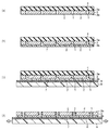
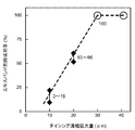
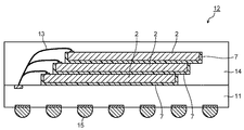
- ダイシング溝により個片化された複数のチップ領域を有し、素子形成面である第1の面に貼付された表面保護フィルムでウエハ形状が維持された半導体ウエハを用意する工程と、
液状接着剤を、前記ダイシング溝の少なくとも一部に充填しつつ、前記半導体ウエハの前記第1の面とは反対側の第2の面に塗布して接着剤層を形成する工程と、
粘着力を低下させることが可能な粘着層を有する支持シートを、前記半導体ウエハの前記第2の面に前記接着剤層を介して貼付する工程と、
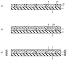
前記半導体ウエハから前記表面保護フィルムを剥離した後、前記支持シートを引き伸ばして前記ダイシング溝内に充填された接着剤を含めて前記接着剤層を割断する工程と、
前記支持シートを引き伸ばした状態を維持しつつ、前記半導体ウエハの第1の面と前記ダイシング溝内を洗浄する工程とを具備し、
前記洗浄工程の前に、前記粘着層の前記ダイシング溝に対応する部分の粘着力を選択的に低下させることを特徴とする半導体装置の製造方法。 - 請求項1記載の半導体装置の製造方法において、
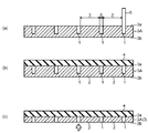
前記粘着層は紫外線硬化型樹脂からなり、
前記粘着層の前記ダイシング溝内に存在する部分に紫外線を選択的に照射し、前記粘着層の粘着力を選択的に低下させることを特徴とする半導体装置の製造方法。 - 請求項1または請求項2記載の半導体装置の製造方法において、
前記接着剤層の形成工程は、前記ダイシング溝内に前記液状接着剤を充填する第1の工程と、前記半導体ウエハの前記第2の面に前記液状接着剤を塗布する第2の工程とを備えることを特徴とする半導体装置の製造方法。
Priority Applications (4)
| Application Number | Priority Date | Filing Date | Title |
|---|---|---|---|
| JP2011022621A JP5659033B2 (ja) | 2011-02-04 | 2011-02-04 | 半導体装置の製造方法 |
| TW100131341A TWI462167B (zh) | 2011-02-04 | 2011-08-31 | 半導體裝置及其製造方法 |
| CN201110273231.6A CN102629594B (zh) | 2011-02-04 | 2011-09-15 | 半导体装置及其制造方法 |
| US13/233,203 US8513088B2 (en) | 2011-02-04 | 2011-09-15 | Semiconductor device and method for manufacturing the same |
Applications Claiming Priority (1)
| Application Number | Priority Date | Filing Date | Title |
|---|---|---|---|
| JP2011022621A JP5659033B2 (ja) | 2011-02-04 | 2011-02-04 | 半導体装置の製造方法 |
Publications (2)
| Publication Number | Publication Date |
|---|---|
| JP2012164739A JP2012164739A (ja) | 2012-08-30 |
| JP5659033B2 true JP5659033B2 (ja) | 2015-01-28 |
Family
ID=46587821
Family Applications (1)
| Application Number | Title | Priority Date | Filing Date |
|---|---|---|---|
| JP2011022621A Expired - Fee Related JP5659033B2 (ja) | 2011-02-04 | 2011-02-04 | 半導体装置の製造方法 |
Country Status (4)
| Country | Link |
|---|---|
| US (1) | US8513088B2 (ja) |
| JP (1) | JP5659033B2 (ja) |
| CN (1) | CN102629594B (ja) |
| TW (1) | TWI462167B (ja) |
Families Citing this family (41)
| Publication number | Priority date | Publication date | Assignee | Title |
|---|---|---|---|---|
| JP5537515B2 (ja) * | 2011-09-01 | 2014-07-02 | 株式会社東芝 | 積層型半導体装置の製造方法と製造装置 |
| JP6030938B2 (ja) * | 2012-12-07 | 2016-11-24 | リンテック株式会社 | シート貼付装置およびシート貼付方法 |
| JP6021687B2 (ja) * | 2013-02-25 | 2016-11-09 | 株式会社ディスコ | 積層ウェーハの加工方法 |
| CN103847032B (zh) * | 2014-03-20 | 2016-01-06 | 德清晶辉光电科技有限公司 | 一种大直径超薄石英晶片的生产工艺 |
| JP6215755B2 (ja) * | 2014-04-14 | 2017-10-18 | ルネサスエレクトロニクス株式会社 | 半導体装置 |
| JP6438304B2 (ja) * | 2015-01-09 | 2018-12-12 | 株式会社ディスコ | ウエーハの加工方法 |
| JP6438791B2 (ja) * | 2015-02-06 | 2018-12-19 | リンテック株式会社 | 半導体装置の製造方法 |
| JP6566703B2 (ja) * | 2015-04-27 | 2019-08-28 | 株式会社ディスコ | デバイスチップの製造方法 |
| US9679785B2 (en) * | 2015-07-27 | 2017-06-13 | Semtech Corporation | Semiconductor device and method of encapsulating semiconductor die |
| JP2017041574A (ja) * | 2015-08-21 | 2017-02-23 | 株式会社ディスコ | ウエーハの加工方法 |
| JP6492288B2 (ja) * | 2015-10-01 | 2019-04-03 | パナソニックIpマネジメント株式会社 | 素子チップの製造方法 |
| JP2017168736A (ja) | 2016-03-17 | 2017-09-21 | 株式会社ディスコ | ウエーハの加工方法 |
| US10204893B2 (en) | 2016-05-19 | 2019-02-12 | Invensas Bonding Technologies, Inc. | Stacked dies and methods for forming bonded structures |
| JP6751337B2 (ja) * | 2016-11-09 | 2020-09-02 | 株式会社ディスコ | 接着フィルムの破断方法 |
| JP2018085482A (ja) * | 2016-11-25 | 2018-05-31 | 積水化学工業株式会社 | 接着剤部付き分割後半導体ウェハ、及び半導体装置の製造方法 |
| JP6789083B2 (ja) * | 2016-11-25 | 2020-11-25 | 積水化学工業株式会社 | 接着剤部付き分割後半導体ウェハ、及び半導体装置の製造方法 |
| JP6773535B2 (ja) * | 2016-11-25 | 2020-10-21 | 積水化学工業株式会社 | 半導体装置の製造方法 |
| US20180182665A1 (en) | 2016-12-28 | 2018-06-28 | Invensas Bonding Technologies, Inc. | Processed Substrate |
| JP2018113281A (ja) * | 2017-01-06 | 2018-07-19 | 株式会社ディスコ | 樹脂パッケージ基板の加工方法 |
| JP6896472B2 (ja) * | 2017-03-23 | 2021-06-30 | 株式会社ディスコ | ウエーハの研磨方法及び研磨装置 |
| JP7086528B2 (ja) * | 2017-04-17 | 2022-06-20 | 株式会社アムコー・テクノロジー・ジャパン | 半導体素子及び半導体装置 |
| JP6949421B2 (ja) * | 2017-05-09 | 2021-10-13 | 株式会社ディスコ | 加工方法 |
| US10879212B2 (en) | 2017-05-11 | 2020-12-29 | Invensas Bonding Technologies, Inc. | Processed stacked dies |
| JP2018198241A (ja) * | 2017-05-23 | 2018-12-13 | 株式会社ディスコ | ウェーハの加工方法 |
| US10363629B2 (en) * | 2017-06-01 | 2019-07-30 | Applied Materials, Inc. | Mitigation of particle contamination for wafer dicing processes |
| JP6866038B2 (ja) * | 2017-06-21 | 2021-04-28 | 株式会社ディスコ | パッケージデバイスの製造方法 |
| CN107464780B (zh) * | 2017-08-01 | 2018-07-20 | 四川科尔威光电科技有限公司 | 一种优化侧壁金属化基板金属毛刺的切割方法 |
| CN107799394A (zh) * | 2017-09-26 | 2018-03-13 | 合肥新汇成微电子有限公司 | 一种半导体晶圆的保护方法 |
| JP6994965B2 (ja) * | 2018-01-29 | 2022-02-04 | 株式会社ディスコ | ダイボンド用樹脂の敷設方法 |
| US11276676B2 (en) | 2018-05-15 | 2022-03-15 | Invensas Bonding Technologies, Inc. | Stacked devices and methods of fabrication |
| CN108597989B (zh) * | 2018-05-29 | 2020-12-22 | 阜阳市恒祥生产力促进有限公司 | 一种半导体晶圆扩晶工艺 |
| WO2020010136A1 (en) | 2018-07-06 | 2020-01-09 | Invensas Bonding Technologies, Inc. | Molded direct bonded and interconnected stack |
| WO2020010265A1 (en) | 2018-07-06 | 2020-01-09 | Invensas Bonding Technologies, Inc. | Microelectronic assemblies |
| US12406959B2 (en) | 2018-07-26 | 2025-09-02 | Adeia Semiconductor Bonding Technologies Inc. | Post CMP processing for hybrid bonding |
| US11296044B2 (en) | 2018-08-29 | 2022-04-05 | Invensas Bonding Technologies, Inc. | Bond enhancement structure in microelectronics for trapping contaminants during direct-bonding processes |
| KR20210104742A (ko) | 2019-01-14 | 2021-08-25 | 인벤사스 본딩 테크놀로지스 인코포레이티드 | 접합 구조체 |
| US11296053B2 (en) | 2019-06-26 | 2022-04-05 | Invensas Bonding Technologies, Inc. | Direct bonded stack structures for increased reliability and improved yield in microelectronics |
| US12080672B2 (en) | 2019-09-26 | 2024-09-03 | Adeia Semiconductor Bonding Technologies Inc. | Direct gang bonding methods including directly bonding first element to second element to form bonded structure without adhesive |
| US11631647B2 (en) | 2020-06-30 | 2023-04-18 | Adeia Semiconductor Bonding Technologies Inc. | Integrated device packages with integrated device die and dummy element |
| CN114464088A (zh) * | 2022-01-07 | 2022-05-10 | 南京冠石科技股份有限公司 | 一种条型sus点胶注塑成品及其加工方法 |
| JP2025021317A (ja) * | 2023-07-31 | 2025-02-13 | 株式会社東芝 | 半導体装置の製造方法および半導体装置 |
Family Cites Families (18)
| Publication number | Priority date | Publication date | Assignee | Title |
|---|---|---|---|---|
| JPS5792848A (en) * | 1980-11-29 | 1982-06-09 | Nec Home Electronics Ltd | Manufacture of semiconductor pellet |
| JPH05206267A (ja) * | 1992-01-29 | 1993-08-13 | Fujitsu Ltd | 半導体装置の製造方法 |
| US5665446A (en) * | 1995-11-16 | 1997-09-09 | Minnesota Mining And Manufacturing Company | Laminate for precise application of graphics to a substrate |
| JP4301596B2 (ja) * | 1998-06-12 | 2009-07-22 | 三菱電機株式会社 | 電子デバイスの製造方法および該製造方法に用いるスリット滴下ノズル |
| JP2001284497A (ja) * | 2000-04-03 | 2001-10-12 | Fujitsu Ltd | 半導体装置及びその製造方法及び半導体チップ及びその製造方法 |
| JP4822482B2 (ja) * | 2001-05-23 | 2011-11-24 | シチズン電子株式会社 | 発光ダイオードおよびその製造方法 |
| KR100468748B1 (ko) * | 2002-07-12 | 2005-01-29 | 삼성전자주식회사 | 프리컷 다이싱 테이프와 범용 다이싱 테이프를 웨이퍼에 마운팅할 수 있는 다이싱 테이프 부착 장비 및 이를포함하는 인라인 시스템 |
| JP2004066017A (ja) * | 2002-08-01 | 2004-03-04 | Nippon Paint Co Ltd | ソルダーレジスト膜の形成方法 |
| JP3978514B2 (ja) * | 2002-12-24 | 2007-09-19 | 株式会社ナノテム | 発光素子の製造方法および発光素子 |
| JP4923398B2 (ja) | 2004-09-21 | 2012-04-25 | 日立化成工業株式会社 | 接着剤層付き半導体素子の製造方法 |
| JP2006120850A (ja) | 2004-10-21 | 2006-05-11 | Anritsu Corp | 半導体チップの製造方法 |
| JP2006332078A (ja) * | 2005-05-23 | 2006-12-07 | Matsushita Electric Ind Co Ltd | 半導体チップの製造方法 |
| JP2008114195A (ja) * | 2006-11-08 | 2008-05-22 | Tokyo Ohka Kogyo Co Ltd | 平坦化塗布方法 |
| US7833881B2 (en) * | 2007-03-02 | 2010-11-16 | Micron Technology, Inc. | Methods for fabricating semiconductor components and packaged semiconductor components |
| JP4859716B2 (ja) * | 2007-03-14 | 2012-01-25 | オンセミコンダクター・トレーディング・リミテッド | ウエハ及びその搬送システム |
| JP4818187B2 (ja) * | 2007-04-16 | 2011-11-16 | 株式会社東芝 | 半導体装置の製造方法 |
| JP2009152493A (ja) * | 2007-12-21 | 2009-07-09 | Shinko Electric Ind Co Ltd | 半導体装置の製造方法 |
| CN101567301B (zh) * | 2008-04-21 | 2010-09-29 | 力成科技股份有限公司 | 粘性晶粒由晶圆分离的形成方法 |
-
2011
- 2011-02-04 JP JP2011022621A patent/JP5659033B2/ja not_active Expired - Fee Related
- 2011-08-31 TW TW100131341A patent/TWI462167B/zh active
- 2011-09-15 US US13/233,203 patent/US8513088B2/en active Active
- 2011-09-15 CN CN201110273231.6A patent/CN102629594B/zh active Active
Also Published As
| Publication number | Publication date |
|---|---|
| TWI462167B (zh) | 2014-11-21 |
| CN102629594A (zh) | 2012-08-08 |
| JP2012164739A (ja) | 2012-08-30 |
| US20120199993A1 (en) | 2012-08-09 |
| TW201234447A (en) | 2012-08-16 |
| CN102629594B (zh) | 2014-11-12 |
| US8513088B2 (en) | 2013-08-20 |
Similar Documents
| Publication | Publication Date | Title |
|---|---|---|
| JP5659033B2 (ja) | 半導体装置の製造方法 | |
| JP4544231B2 (ja) | 半導体チップの製造方法 | |
| TWI463556B (zh) | Semiconductor device manufacturing method and manufacturing device | |
| US7932614B2 (en) | Method of thinning a semiconductor substrate | |
| JP6524594B2 (ja) | 素子チップの製造方法 | |
| TW201501222A (zh) | 半導體晶片之製造方法 | |
| JP6305355B2 (ja) | デバイスの製造方法 | |
| JP2011233711A (ja) | 半導体装置の製造方法 | |
| JP6162578B2 (ja) | ウェーハの分割方法 | |
| JP2008066653A (ja) | ウェーハ処理方法およびウェーハ処理装置 | |
| JP2009259999A (ja) | 熱硬化接着剤付き半導体チップの製造方法 | |
| CN107564950B (zh) | 晶圆、半导体封装件及其制造方法 | |
| JP5918639B2 (ja) | ウェーハの処理方法 | |
| JP2007180252A (ja) | 半導体装置の製造方法 | |
| JP5540842B2 (ja) | 半導体装置の製造方法 | |
| JP3173464B2 (ja) | 半導体装置の製造方法 | |
| JP2004179565A (ja) | 電子部品の製造方法及びダイシング方法、並びにこれらを実施するための製造装置 | |
| CN106298493A (zh) | 半导体装置的制造方法 | |
| TWI702646B (zh) | 晶圓切割微粒移除方法 | |
| JP2021015938A (ja) | 水溶性の樹脂シート及びウェーハの加工方法 | |
| JP5148298B2 (ja) | 半導体装置の製造方法 | |
| JP2017112269A (ja) | ウエーハの加工方法 | |
| JP2024154576A (ja) | ダイアタッチフィルム及び半導体装置の製造方法 | |
| CN112838056A (zh) | 一种用于制造半导体芯片的方法 | |
| CN120613270A (zh) | 一种封装体单元化分离方法 |
Legal Events
| Date | Code | Title | Description |
|---|---|---|---|
| A621 | Written request for application examination |
Free format text: JAPANESE INTERMEDIATE CODE: A621 Effective date: 20130215 |
|
| A977 | Report on retrieval |
Free format text: JAPANESE INTERMEDIATE CODE: A971007 Effective date: 20131209 |
|
| A131 | Notification of reasons for refusal |
Free format text: JAPANESE INTERMEDIATE CODE: A131 Effective date: 20140212 |
|
| A521 | Request for written amendment filed |
Free format text: JAPANESE INTERMEDIATE CODE: A523 Effective date: 20140409 |
|
| TRDD | Decision of grant or rejection written | ||
| A01 | Written decision to grant a patent or to grant a registration (utility model) |
Free format text: JAPANESE INTERMEDIATE CODE: A01 Effective date: 20141104 |
|
| A61 | First payment of annual fees (during grant procedure) |
Free format text: JAPANESE INTERMEDIATE CODE: A61 Effective date: 20141201 |
|
| R151 | Written notification of patent or utility model registration |
Ref document number: 5659033 Country of ref document: JP Free format text: JAPANESE INTERMEDIATE CODE: R151 |
|
| S111 | Request for change of ownership or part of ownership |
Free format text: JAPANESE INTERMEDIATE CODE: R313111 |
|
| R350 | Written notification of registration of transfer |
Free format text: JAPANESE INTERMEDIATE CODE: R350 |
|
| S111 | Request for change of ownership or part of ownership |
Free format text: JAPANESE INTERMEDIATE CODE: R313111 |
|
| R350 | Written notification of registration of transfer |
Free format text: JAPANESE INTERMEDIATE CODE: R350 |
|
| LAPS | Cancellation because of no payment of annual fees |