JP5659033B2 - Manufacturing method of semiconductor device - Google Patents
Manufacturing method of semiconductor device Download PDFInfo
- Publication number
- JP5659033B2 JP5659033B2 JP2011022621A JP2011022621A JP5659033B2 JP 5659033 B2 JP5659033 B2 JP 5659033B2 JP 2011022621 A JP2011022621 A JP 2011022621A JP 2011022621 A JP2011022621 A JP 2011022621A JP 5659033 B2 JP5659033 B2 JP 5659033B2
- Authority
- JP
- Japan
- Prior art keywords
- adhesive layer
- adhesive
- semiconductor wafer
- dicing
- semiconductor
- Prior art date
- Legal status (The legal status is an assumption and is not a legal conclusion. Google has not performed a legal analysis and makes no representation as to the accuracy of the status listed.)
- Expired - Fee Related
Links
Images


Classifications
-
- H—ELECTRICITY
- H10—SEMICONDUCTOR DEVICES; ELECTRIC SOLID-STATE DEVICES NOT OTHERWISE PROVIDED FOR
- H10P—GENERIC PROCESSES OR APPARATUS FOR THE MANUFACTURE OR TREATMENT OF DEVICES COVERED BY CLASS H10
- H10P54/00—Cutting or separating of wafers, substrates or parts of devices
-
- H—ELECTRICITY
- H10—SEMICONDUCTOR DEVICES; ELECTRIC SOLID-STATE DEVICES NOT OTHERWISE PROVIDED FOR
- H10W—GENERIC PACKAGES, INTERCONNECTIONS, CONNECTORS OR OTHER CONSTRUCTIONAL DETAILS OF DEVICES COVERED BY CLASS H10
- H10W72/00—Interconnections or connectors in packages
- H10W72/01—Manufacture or treatment
- H10W72/011—Apparatus therefor
- H10W72/0113—Apparatus for manufacturing die-attach connectors
Landscapes
- Dicing (AREA)
- Die Bonding (AREA)
- Container, Conveyance, Adherence, Positioning, Of Wafer (AREA)
Description
本発明の実施形態は半導体装置の製造方法に関する。 Embodiments described herein relate generally to a method for manufacturing a semiconductor device.
半導体装置(半導体チップ)の製造工程は、半導体ウエハの表面側にチップ領域に応じて半導体回路や配線層等を有する半導体素子部を形成する工程と、半導体ウエハをチップ領域(チップ形状)に応じて切断(個片化)する工程とに大別される。半導体ウエハを加工するにあたって、ウエハの薄厚化とチップの個片化とを兼ねる加工工程として、先ダイシングと呼ばれる工程が適用されている。先ダイシング工程においては、まず半導体ウエハに半導体素子部が形成された表面側からウエハ厚より浅く、チップ完成厚より深い溝を形成する。次いで、半導体ウエハの表面に保護フィルムを貼り付けた後、半導体ウエハの裏面を研削して半導体ウエハを各チップに個片化する。 The manufacturing process of the semiconductor device (semiconductor chip) includes a step of forming a semiconductor element portion having a semiconductor circuit, a wiring layer, etc. on the surface side of the semiconductor wafer according to the chip region, and a step of forming the semiconductor wafer in accordance with the chip region (chip shape) It is roughly divided into a process of cutting (dividing into pieces). In processing a semiconductor wafer, a process called pre-dicing is applied as a processing process that serves both as a thinning of the wafer and chip separation. In the first dicing step, first, a groove that is shallower than the wafer thickness and deeper than the finished chip thickness is formed from the surface side where the semiconductor element portion is formed on the semiconductor wafer. Next, after a protective film is attached to the front surface of the semiconductor wafer, the back surface of the semiconductor wafer is ground to separate the semiconductor wafer into individual chips.
次に、表面保護フィルムで全体形状が維持されている半導体ウエハの裏面に、シート状の接着剤フィルムと支持フィルムとを貼り付ける。接着剤フィルムは各チップの接着剤層として機能させるものであるため、各チップ形状に応じて切断(個片化)される。接着剤フィルムは、例えば表面保護フィルムを剥離した後、半導体ウエハの表面側からダイシング溝に沿ってレーザ光を照射することにより切断される。また、半導体ウエハが貼り付けられた支持フィルムを水平方向に引き伸ばし、チップ間に存在する接着剤フィルムを選択的に改質することによって、接着剤フィルムを切断する方法等も提案されている。 Next, a sheet-like adhesive film and a support film are attached to the back surface of the semiconductor wafer whose overall shape is maintained by the surface protective film. Since the adhesive film functions as an adhesive layer of each chip, it is cut (divided) according to the shape of each chip. The adhesive film is cut by, for example, irradiating laser light along the dicing grooves from the surface side of the semiconductor wafer after peeling off the surface protective film. In addition, a method of cutting the adhesive film by stretching the support film on which the semiconductor wafer is attached in the horizontal direction and selectively modifying the adhesive film existing between the chips has been proposed.
接着剤フィルムをレーザ光で切断する方法は、半導体ウエハの貼り付けを繰り返す中でチップの整列性が低下しやすいため、接着剤フィルムの切断速度が低下して切断工数が増大しやすい。また、接着剤フィルムをレーザ光で切断する際に発生する屑が半導体チップを汚染するおそれがある。接着剤フィルムを選択的に改質する方法は、改質に要するコストが切断コストを増大させやすく、また改質方法によっては接着剤フィルムの切断性を十分に高められないおそれもある。そこで、先ダイシング等によりチップ形状に個片化された半導体ウエハの裏面に接着剤層を形成するにあたって、接着剤層の切断性を高めると共に、接着剤層の切断時における半導体チップの汚染等を抑制することが求められている。 In the method of cutting the adhesive film with a laser beam, the alignment of the chips tends to be lowered while the semiconductor wafer is repeatedly attached, so that the cutting speed of the adhesive film is lowered and the number of cutting steps is easily increased. Moreover, there is a possibility that waste generated when cutting the adhesive film with laser light will contaminate the semiconductor chip. In the method of selectively modifying the adhesive film, the cost required for the modification tends to increase the cutting cost, and the cutting property of the adhesive film may not be sufficiently improved depending on the modification method. Therefore, when forming the adhesive layer on the back surface of the semiconductor wafer separated into chips by tip dicing or the like, the cutting ability of the adhesive layer is improved and the contamination of the semiconductor chip at the time of cutting the adhesive layer is reduced. There is a need to suppress it.
本発明が解決しようとする課題は、個片化された半導体チップを有する半導体ウエハの裏面に形成した接着剤層の切断性を高めて製造コストの低減を図ると共に、接着剤層の切断屑等による半導体チップの汚染等を抑制して製造歩留りを高めることを可能にした半導体装置の製造方法を提供することにある。 The problem to be solved by the present invention is to improve the cutting property of the adhesive layer formed on the back surface of the semiconductor wafer having the separated semiconductor chips to reduce the manufacturing cost, and to cut the adhesive layer, etc. It is an object of the present invention to provide a method for manufacturing a semiconductor device that can increase the manufacturing yield by suppressing contamination of the semiconductor chip due to the above.
実施形態の半導体装置の製造方法は、ダイシング溝により個片化された複数のチップ領域を有し、素子形成面である第1の面に貼付された表面保護フィルムでウエハ形状が維持された半導体ウエハを用意する工程と、液状接着剤をダイシング溝の少なくとも一部に充填しつつ、半導体ウエハの第1の面とは反対側の第2の面に塗布して接着剤層を形成する工程と、粘着力を低下させることが可能な粘着層を有する支持シートを、半導体ウエハの第2の面に接着剤層を介して貼付する工程と、半導体ウエハから表面保護フィルムを剥離した後、支持シートを引き伸ばしてダイシング溝内に充填された接着剤および接着剤層を割断する工程と、支持シートを引き伸ばした状態を維持しつつ、前記半導体ウエハの第1の面とダイシング溝内を洗浄する工程とを具備している。粘着層のダイシング溝に対応する部分の粘着力を、洗浄工程の前に選択的に低下させる。 A method of manufacturing a semiconductor device according to an embodiment includes a semiconductor having a plurality of chip regions separated by dicing grooves and having a wafer shape maintained by a surface protective film attached to a first surface that is an element formation surface A step of preparing a wafer, a step of applying an adhesive layer to a second surface opposite to the first surface of the semiconductor wafer while filling at least a part of the dicing groove with a liquid adhesive, and a step of forming an adhesive layer A step of attaching a support sheet having an adhesive layer capable of reducing the adhesive force to the second surface of the semiconductor wafer via an adhesive layer; and a support sheet after peeling the surface protective film from the semiconductor wafer. The first surface of the semiconductor wafer and the inside of the dicing groove are cleaned while maintaining the stretched state of the support sheet and the step of cleaving the adhesive and the adhesive layer filled in the dicing groove by stretching It is provided with a step. The adhesive strength of the portion corresponding to the dicing groove of the adhesive layer is selectively reduced before the cleaning step.
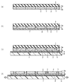
以下、実施形態の半導体装置の製造方法について、図面を参照して説明する。図1は実施形態による半導体装置の製造方法を示す図である。図2ないし図5は実施形態の半導体装置の製造方法における各工程を示す図である。まず、図1(a)に示すように、ダイシング溝1により個片化された複数のチップ領域2、2…を有する半導体ウエハ3を用意する。半導体ウエハ3は各チップ領域2に個片化されているものの、素子形成面である第1の面3aに貼付された表面保護フィルム4でウエハ形状が維持されている。このような半導体ウエハ3は、例えば先ダイシング工程により作製される。
Hereinafter, a method for manufacturing a semiconductor device according to an embodiment will be described with reference to the drawings. FIG. 1 is a diagram illustrating a method of manufacturing a semiconductor device according to an embodiment. 2 to 5 are diagrams showing each step in the semiconductor device manufacturing method of the embodiment. First, as shown in FIG. 1A, a
半導体ウエハ3の先ダイシング工程について、図2を参照して述べる。図2(a)に示すように、半導体回路や配線層等を有する半導体素子部が形成された半導体ウエハ3Aを用意する。半導体ウエハ3Aは素子形成面である第1の面(表面)3aとそれとは反対側の第2の面(裏面)3bとを有している。半導体ウエハ3Aは複数の複数のチップ領域2、2…を有しており、各チップ領域2の第1の面3a側には半導体回路や配線層等を有する半導体素子部が形成されている。複数のチップ領域2間にはダイシング領域5が設けられており、このダイシング領域5に沿って半導体ウエハ3Aを切断することによって、複数のチップ領域2、2…をそれぞれ個片化して半導体チップを作製する。
The tip dicing process of the
半導体ウエハ3Aを切断するにあたって、まず図2(a)に示すように、半導体ウエハ3Aに第1の面3a側からダイシング領域5に沿って溝1を形成する。半導体ウエハ3Aの溝1は、例えばダイシング領域5の幅に応じた刃厚を有するブレード6を用いて形成される。溝1の深さは半導体ウエハ3Aの厚さより浅く、かつ半導体チップの完成時の厚さより深く設定される。溝1はエッチング等で形成してもよい。このような深さの溝(ダイシング溝)1を半導体ウエハ3Aに形成することによって、複数のチップ領域2、2…はそれぞれ半導体チップの完成厚さに応じた状態に区分される。
When cutting the
次いで、図2(b)に示すように、ダイシング溝1を形成した半導体ウエハ3Aの第1の面3aに表面保護フィルム4を貼付する。表面保護フィルム4は後工程で半導体ウエハ3Aの第2の面(裏面)3bを研削する際に、チップ領域2に設けられた半導体素子部を保護すると共に、第2の面3bの研削工程でチップ領域2を個片化した後の半導体ウエハ3Aの形状を維持するものである。表面保護フィルム4としては、例えば粘着層を有するポリエチレンテレフタレート(PET)フィルムのような樹脂フィルムが用いられる。
Next, as shown in FIG. 2B, a surface protective film 4 is attached to the
次に、図2(c)に示すように、表面保護フィルム4を貼付した半導体ウエハ3Aの第2の面(裏面)3bを研削および研磨する。半導体ウエハ3Aの第2の面3bは、例えばラッピング定盤を用いて機械的に研削され、続いて研磨定盤を用いて研磨(例えばドライポリッシング)される。半導体ウエハ3Aの第2の面3bの研削・研磨工程は、第1の面3a側から形成したダイシング溝1に達するように実施される。このように、半導体ウエハ3Aの第2の面3bを研削することで、各チップ領域2はそれぞれ個片化される。
Next, as shown in FIG.2 (c), the 2nd surface (back surface) 3b of the
この段階において、各チップ領域2は個片化されているものの、表面保護フィルム4で保持されているため、全体的にはウエハ形状が維持されている。すなわち、図2(c)に示すように、ダイシング溝1により個片化された複数のチップ領域2、2…を有し、素子形成面である第1の面3aに貼付された表面保護フィルム4でウエハ形状が維持された半導体ウエハ3が作製される。個片化されたチップ領域2間には、ダイシング溝1の幅に相当する隙間が存在している。なお、半導体ウエハ3の作製工程は先ダイシング工程に限られるものではなく、レーザ光によるダイシング工程等を適用してもよい。
At this stage, although each
次に、図1(b)に示すように、表面保護フィルム4で全体形状が維持されている半導体ウエハ3の第2の面3bに、液状接着剤を塗布して接着剤層7を形成する。液状接着剤はダイシング溝1の少なくとも一部に充填しつつ、半導体ウエハ3の第2の面3bに塗布される。液状接着剤としては、例えばエポキシ樹脂やポリイミド樹脂のような熱硬化性樹脂の液状組成物が用いられる。また、光および熱硬化型の樹脂や水分蒸発と再湿により可逆的に硬化する(再活性接着)樹脂の液状組成物等を使用することも可能である。
Next, as shown in FIG. 1B, a liquid adhesive is applied to the
半導体ウエハ3の第2の面3bに液状接着剤を塗布する方法としては、例えばインクジェット法、スプレー法、ロールコーター法、スクリーン印刷法等を適用することができる。なかでも、半導体ウエハ3と非接触な状態で液状接着剤を塗布することが可能なインクジェット法やスプレー法を適用することがより好ましい。さらに、インクジェット法によれば膜厚の薄い液状接着剤の塗布層を比較的均一に形成することができるため、インクジェット法は半導体ウエハ3への液状接着剤の塗布方法として好適である。
As a method of applying the liquid adhesive to the
接着剤層7は、個片化した半導体チップ(チップ領域2)を配線基板や他の半導体チップ上に実装する際に接着層として機能するものであり、半導体チップの外形に応じて切断(個片化)されるものである。このような接着剤層7の厚さは1μm以上20μm以下とすることが好ましい。接着剤層7は、次工程の前に室温では粘着力(タック力)を示さない状態としておくことが好ましい。例えば、液状接着剤として熱硬化性樹脂の液状組成物(Aステージ)を用いた場合、接着剤層7は液状接着剤の塗布層を所定の温度で乾燥させて半硬化状態(Bステージ)としておくことが好ましい。熱硬化性以外の樹脂を用いた場合にも、硬化形態に応じた処理を施しておくことが好ましい。
The
ところで、予めダイシング溝1が形成されている半導体ウエハ3の第2の面3bに液状接着剤を塗布して接着剤層7を形成するにあたって、単に液状接着剤を半導体ウエハ3の全面に塗布しただけではダイシング溝1内に液状接着剤が流れ込むことで、各チップ領域2上の接着剤層7の膜厚を均一化することが難しい。例えば、膜厚が10μmの接着剤層7を形成しようとしたときに、液状接着剤を半導体ウエハ3の全面に塗布しただけでは、チップ領域(サイズ:11×13mm)2の中央部の厚さが20μm程度となり、かつ端部から50μmの位置での厚さが1〜2μm程度となってしまう。接着剤層7の膜厚が不均一であると、後工程のダイボンディング工程で接着不良が生じやすくなる。
By the way, in forming the
このような点に対して、ダイシング溝1内に液状接着剤を充填する第1の工程と、半導体ウエハ3の第2の面3bに液状接着剤を塗布する第2の工程とを有する接着剤層7の形成工程を適用することが好ましい。接着剤層7の形成工程について、図3を参照して述べる。まず、図3(a)に示すように、幅が30〜40μm程度のダイシング溝1内に液状接着剤7Aを充填する。この際、各チップ領域2は半導体ウエハ3(3A)のダイシング時に整列性が低下している(ダイシング溝1がずれている)おそれがあるため、ダイシング溝1の幅以上(例えば溝幅の1.5倍以上3倍以下)に塗布することによって、ダイシング溝1内に液状接着剤7Aを充填することが好ましい。
For such a point, an adhesive having a first step of filling the dicing
次に、図3(b)に示すように、ダイシング溝1内に液状接着剤7Aを充填した半導体ウエハ3の第2の面3b全体に液状接着剤7Aを塗布する。この段階において、液状接着剤7Aを半導体ウエハ3の全面に単に塗布した場合に比べて、各チップ領域2内の接着剤層7の膜厚の面内均一性を大幅に高めることができる。ただし、ダイシング溝1内に液状接着剤7Aを充填した際の第2の面3bへの盛り上がりや充填時における液状接着剤7Aのダイシング溝1からのずれ等によって、部分的に接着剤層7の膜厚が不均一になる場合がある。そのような場合には、図3(c)に示すように、液状接着剤7Aを塗布した半導体ウエハ3全体を揺動させて液状接着剤7Aの塗布厚を均一化する(液状接着剤7Aの塗布層の凹凸部分を平坦化する)ことが好ましい。
Next, as shown in FIG. 3B, the liquid adhesive 7A is applied to the entire
半導体ウエハ3を揺動させる方法としては、半導体ウエハ3を機械的に前後左右に揺らす、半導体ウエハ3に歳差運動を加える、半導体ウエハ3に超音波を印加する等が挙げられる。このような方法で半導体ウエハ3を揺動させることによって、液状接着剤7Aの塗布層の凹凸部分を平坦化し、接着剤層7の膜厚の面内均一性をより一層高める、例えば接着剤層7の膜厚の面内ばらつきを30%以下にすることが可能となる。膜厚の面内ばらつきは、チップ領域2内の接着剤層7の膜厚を測定して最大値と最小値を求め、[{(最大値−最小値)/(最大値+最小値)}×100(%)]の式から求める。
Examples of the method of swinging the
例えば、サイズが11×13mmのチップ領域2に膜厚が10μmの接着剤層7を形成する際に、まず幅が30〜40μmのダイシング溝1内に液状接着剤7Aを充填(充填幅=溝幅の1.5倍)した後、半導体ウエハ3の第2の面3bに液状接着剤7Aを塗布し、さらに半導体ウエハ3全体を揺動させた場合、チップ領域2の中央部の厚さを13μm程度とすることができ、さらにチップ領域2の端部の厚さを7μm程度とすることができる。この膜厚の面内ばらつき(膜厚の面内分布)を上式に当てはめて計算すると、{(13−7)/(13+7)}×100=30(%)となる。
For example, when the
チップ領域2内における接着剤層7の膜厚の面内均一性を高めることで、半導体チップのダイボンディング工程における接着不良を抑制することができる。さらに、ダイシング溝1内に接着剤を充填しつつ、接着剤層7の膜厚の面内均一性を高めることによって、後工程の接着剤層7の割断工程の成功率を向上させることが可能となる。すなわち、後述する引き伸ばし工程時において、ダイシング溝1内に充填された接着剤に割断の起点が生じるため、接着剤層7の割断性を高めることができる。加えて、ダイシング溝1内に充填された接着剤は、半導体チップの側面を保護する層として機能させることができる。
By increasing the in-plane uniformity of the film thickness of the
次に、図1(c)に示すように、粘着層8を有する支持シート9を、接着剤層7を介して半導体ウエハ3の第2の面3bに貼付する。支持シート9は粘着層8が接着剤層7と接するように半導体ウエハ3に貼付される。粘着層8は粘着力を低下させることが可能な材料からなり、例えば紫外線の照射により硬化して粘着力が低下する紫外線硬化型樹脂、レーザ光等の照射により硬化して粘着力が低下する光および熱硬化型樹脂、接着剤層7を構成する樹脂との熱膨張差に基づいて冷却時に粘着力が低下する樹脂等が使用される。粘着層8を有する支持シート9としては、例えば紫外線硬化型粘着テープ(例えば、ポリエチレンやポリプロピレンのようなポリオレフィン樹脂、ポリ塩化ビニル樹脂等からなる基材シートに紫外線硬化型樹脂からなる粘着層を形成したテープ)を用いることができる。
Next, as shown in FIG. 1C, a
図1(d)に示すように、半導体ウエハ3から表面保護フィルム4を剥離した後、支持シート9を水平方向(半導体ウエハ3の各面3a、3bに平行な方向)に引き伸ばす(エキスパンド)して、ダイシング溝1内に充填された接着剤を含めて接着剤層7を割断する。このように、接着剤層7をチップ領域2の形状に合わせて割断することによって、各チップ領域2に接着剤層7を形成する。すなわち、個片化された接着剤層7を有するチップ領域2、言い換えると個片形状の接着剤層7を有する半導体チップを作製する。
As shown in FIG. 1D, after the surface protective film 4 is peeled off from the
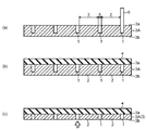
上述した接着剤層7の割断工程に先立って、粘着層8のダイシング溝1に対応する部分の粘着力を選択的に低下させる。例えば、粘着層8が紫外線硬化型樹脂からなる場合には、図4(a)に示すように、半導体ウエハ3の第1の面3a側から紫外線Xを照射する。半導体ウエハ3の第1の面3aに照射された紫外線Xは、各チップ領域2がマスクとなって紫外線Xを遮断するため、ダイシング溝1内のみを透過して粘着層8のダイシング溝1に対応する部分を選択的に硬化させる。すなわち、粘着層8のダイシング溝1に対応する部分の粘着力を選択的に低下させることができる。
Prior to the cleaving step of the
また、粘着層8として光および熱硬化型の樹脂を用いた場合には、例えばレーザ光をダイシング溝1内に照射することによって、粘着層8のダイシング溝1に対応する部分の粘着力を低下させる。この際、レーザ光のフォーカスを粘着層8に合わせることによって、ダイシング溝1内の接着剤層7を硬化させることなく、粘着層8のダイシング溝1に対応する部分のみを選択的に硬化させることができる。すなわち、粘着層8のダイシング溝1に対応する部分の粘着力を選択的に低下させることができる。他の樹脂を用いる場合にも粘着力の低下形態に応じた処理を適用することによって、粘着層8のダイシング溝1に対応する部分の粘着力を選択的に低下させる。
Further, when light and thermosetting resin are used as the
このように、粘着層8のダイシング溝1に対応する部分の粘着力を選択的に低下させた後に支持シート9を水平方向に引き伸ばすことで、図4(b)に示すように、接着剤層7の粘着層8からの接着状態が解除された部分、すなわちダイシング溝1内で粘着層8と界面を形成している部分に割断の起点Aが生じる。この状態から支持シート9の引き伸ばし量(エキスパンド量)を増加させることによって、図4(c)に示すように、ダイシング溝1内の接着剤を含めて接着剤層7を良好に割断することができる。すなわち、支持シート9の引き伸ばし(エキスパンド)によるダイシング溝1内の接着剤層7の割断性が向上し、これにより接着剤層7の割断成功率を高めることが可能となる。
Thus, after selectively reducing the adhesive force of the part corresponding to the dicing groove |
接着剤層7が例えば紫外線を透過しないような場合には、図5(a)に示すように、支持シート9を水平方向に引き伸ばして接着剤層7の一部を割断した後、支持シート9の引き伸ばし状態を維持しつつ、半導体ウエハ3の第1の面3a側から紫外線Xを照射する。接着剤層7の割断部を介して粘着層8に紫外線Xを照射し、粘着層8のダイシング溝1に対応する部分を選択的に硬化させて粘着力を低下させる。これによって、図5(b)に示すように、ダイシング溝1内に存在する接着剤層7の底部(粘着層8と界面を形成している部分)を良好に割断することができる。
In the case where the
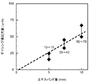
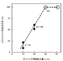
図6に支持シート9の引き伸ばし(エキスパンド)量とダイシング溝1の拡大量との関係を、また図7にダイシング溝1の拡大量と接着剤層7の割断成功率との関係を示す。図6および図7から明らかなように、粘着層8のダイシング溝1に対応する部分の粘着力を選択的に低下させた場合には、ダイシング溝1の拡大量を30μm以上とすることによって、接着剤層7の割断成功率を100%とすることができる。これはダイシング溝1の当初の溝幅には影響されない。すなわち、当初の溝幅にかかわらず、ダイシング溝1の拡大量を30μm以上とすることによって、接着剤層7の割断成功率が大幅に向上する。
FIG. 6 shows the relationship between the amount of expansion (expanding) of the
このように、粘着層8のダイシング溝1に対応する部分の粘着力を選択的に低下させることによって、支持シート9の引き伸ばし工程(エキスパンド工程)における接着剤層7の割断成功率を高めることができる。粘着層8のダイシング溝1に対応する部分の粘着力を選択的に低下させる工程は、支持シート9の引き伸ばし工程前、引き伸ばし工程時、あるいは引き伸ばし工程後のいずれの時期に実施してもよい。場合によっては、粘着シート等の段階(半導体ウエハ3への貼付前)において、粘着層8のダイシング溝1に対応する部分の粘着力を選択的に低下させておいてもよい。粘着層8の粘着力の選択的な低下工程は、後述する洗浄工程前に実施すればよい。
Thus, by selectively reducing the adhesive strength of the portion corresponding to the dicing
さらに、粘着層8のダイシング溝1に対応する部分の粘着力を選択的に低下させることで、接着剤層7の割断による不都合の発生を抑制することができる。粘着層8の粘着力を選択的に低下させない場合には、接着剤層7の割断時に飛散する樹脂片が増加する。加えて、ダイシング溝1内に割断が不十分な部分が生じやすいため、後工程の洗浄工程を実施してもダイシング溝1内に飛散した樹脂片や樹脂残渣等を除去できないおそれがある。ダイシング溝1内の接着剤層7は、図5(a)に示した状態から強制的に引きちぎられるため、割断エッジにバリ(ひげバリ等)が生じ、これが半導体チップのピックアップ時に脱落して電極パッド等を汚染して接続不良を生じさせる。このように、飛散した割断樹脂片や割断エッジに生じるバリ等が半導体チップの不良発生率を増加させる要因となる。
Furthermore, by selectively reducing the adhesive strength of the portion corresponding to the dicing
このような点に対して、粘着層8のダイシング溝1に対応する部分の粘着力を選択的に低下させることによって、接着剤層7(ダイシング溝1内の接着剤層7)の割断性が向上するため、割断時に飛散する樹脂片量を低減することができる。また、ダイシング溝1内に飛散した樹脂片や樹脂残渣等は、後工程の洗浄工程で十分に除去することができる。さらに、割断エッジにおけるバリ(ひげバリ等)の発生を抑制することができる。これらによって、飛散した樹脂片、樹脂残渣、割断エッジに生じたバリ等に起因する半導体チップの不良発生率を低下させることが可能となる。
For such a point, by selectively reducing the adhesive strength of the portion corresponding to the dicing
洗浄工程前に粘着層8の粘着力を選択的に低下させた場合(実施例)と粘着層8の粘着力の選択的な低下を実施しなかった場合(比較例)について、飛散した割断樹脂片やピックアップ時におけるバリの落下等による半導体チップの不良発生率を比較した。なお、いずれも後工程の洗浄工程を実施した。その結果、洗浄工程前に粘着層8の粘着力を選択的に低下させた場合には、半導体チップの不良発生率が0%であったのに対し、粘着層8の粘着力を選択的に低下させなかった場合には、半導体チップの不良発生率が16%にまで上昇した。このように、洗浄工程前に粘着層8の粘着力を選択的に低下させることによって、半導体チップの不良発生率を抑えることができる。この半導体チップの不良発生率の低減と上述した接着剤層7の割断成功率の向上とに基づいて、半導体チップやそれを用いた半導体装置の製造歩留りを大幅に向上させることが可能となる。
When the adhesive strength of the
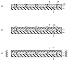
この後、支持シート9の引き伸ばし状態を維持しつつ、半導体ウエハ3の第1の面3aとダイシング溝1内を洗浄する。洗浄工程には、例えば二流体洗浄(加速した空気等の気体に純水等を混入して発生させたミスト(液滴)を、洗浄面に高速で衝突させて洗浄する方法)、超音波洗浄、高温水を使用した超音波洗浄、氷の吹き付けによる洗浄、加熱水蒸気による洗浄等を適用することが好ましい。これらの洗浄方法を適用することで、飛散した樹脂片等が効果的に除去される。さらに、支持シート9の引き伸ばし状態を維持したまま洗浄工程を実施することで、ダイシング溝1内の樹脂片や樹脂残渣等を効果的に除去することができる。従って、半導体チップの不良発生率が低下する。
Thereafter, the
洗浄工程はダイシング溝1内に存在する接着剤を全て除去するように実施してもよいが、チップ領域2の側面に残存する接着剤はそのまま残し、ダイシング溝1内に飛散した樹脂片や樹脂残渣のみを除去するように実施することが好ましい。接着剤層7の割断後にチップ領域2の側面に残存する接着剤は、半導体チップの保護層として機能するため、半導体チップの側面に存在させておくことが好ましい。これによって、半導体チップを樹脂封止する際のフィラーによる半導体チップの損傷等を抑制することができる。
The cleaning process may be performed so as to remove all the adhesive existing in the dicing
上述した各製造工程を経ることによって、チップ領域2にはその形状に応じた接着剤層7が形成される。すなわち、個片形状の接着剤層7を有する半導体チップ(2)が作製される。この実施形態の製造工程によれば、接着剤層7の割断性を向上させると共に、割断時に生じる樹脂片や樹脂残渣等を効果的に除去することを可能にしている。従って、接着剤層7のチップ領域2の形状に応じた切断工程(個片化工程)に要するコストを削減できると共に、割断時に生じる樹脂片、樹脂残渣、バリ等による半導体チップの製造歩留りの低下を抑制することができる。これらによって、例えば先ダイシングを適用した半導体チップの製造工程の低コスト化や高精度化等を実現することができ、さらに後工程の半導体チップの実装工程の信頼性等も向上させることが可能となる。
By passing through each manufacturing process mentioned above, the
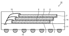
洗浄工程が終了した半導体ウエハ3は、通常の半導体装置の製造工程と同様に、半導体チップ2のピックアップ工程に送られる。すなわち、個片形状の接着剤層7を有する半導体チップ2は、支持シート9からピックアップされた後、例えば図8に示すように配線基板11上に実装される。半導体チップ2の実装は接着剤層7を用いて実施される。半導体チップ2を多段に積層する場合には、図8に示すように配線基板11上に実装された半導体チップ2上に、他の半導体チップ2を接着剤層7により順に積層する。
The
図8において、配線基板11と半導体チップ2とは金属ワイヤ13により電気的に接続されている。半導体チップ2は金属ワイヤ13等と共に封止樹脂層14により封止されている。配線基板11の下面側には外部電極15が設けられている。図8は配線基板11上に複数の半導体チップ2を階段状に積層した半導体装置12を示しているが、半導体装置12には各種公知の構成を適用することができる。例えば、半導体チップ2を実装する回路基材はリードフレームでもよく、また半導体チップ2の積層構造は電極パッドを露出させる交互積層や電極パッド上も他のチップで覆う直上積層等、種々の積層構造を適用することができる。これら以外の構成についても同様である。
In FIG. 8, the
なお、本発明のいくつかの実施形態を説明したが、これらの実施形態は例として提示したものであり、発明の範囲を限定することは意図していない。これら実施形態は、その他の様々な形態で実施し得るものであり、発明の要旨を逸脱しない範囲で、種々の省略、置き換え、変更を行うことができる。これら実施形態やその変形は、発明の範囲や要旨に含まれると同時に、特許請求の範囲に記載された発明とその均等の範囲に含まれる。 In addition, although several embodiment of this invention was described, these embodiment is shown as an example and is not intending limiting the range of invention. These embodiments can be implemented in various other forms, and various omissions, replacements, and changes can be made without departing from the scope of the invention. These embodiments and modifications thereof are included in the scope and gist of the invention, and at the same time included in the invention described in the claims and the equivalents thereof.
1…ダイシング溝、2…チップ領域、3,3A…半導体ウエハ、4…表面保護フィルム、7…接着剤層、7A…液状接着剤、8…粘着層、9…支持シート。
DESCRIPTION OF
Claims (3)
液状接着剤を、前記ダイシング溝の少なくとも一部に充填しつつ、前記半導体ウエハの前記第1の面とは反対側の第2の面に塗布して接着剤層を形成する工程と、
粘着力を低下させることが可能な粘着層を有する支持シートを、前記半導体ウエハの前記第2の面に前記接着剤層を介して貼付する工程と、
前記半導体ウエハから前記表面保護フィルムを剥離した後、前記支持シートを引き伸ばして前記ダイシング溝内に充填された接着剤を含めて前記接着剤層を割断する工程と、
前記支持シートを引き伸ばした状態を維持しつつ、前記半導体ウエハの第1の面と前記ダイシング溝内を洗浄する工程とを具備し、
前記洗浄工程の前に、前記粘着層の前記ダイシング溝に対応する部分の粘着力を選択的に低下させることを特徴とする半導体装置の製造方法。 Preparing a semiconductor wafer having a plurality of chip regions separated by dicing grooves and maintaining the wafer shape with a surface protective film attached to a first surface which is an element forming surface;
Applying a liquid adhesive to a second surface opposite to the first surface of the semiconductor wafer to form an adhesive layer while filling at least a part of the dicing groove;
A step of attaching a support sheet having an adhesive layer capable of reducing the adhesive force to the second surface of the semiconductor wafer via the adhesive layer;
Cleaving the adhesive layer including the adhesive filled in the dicing grooves by stretching the support sheet after peeling the surface protective film from the semiconductor wafer;
Cleaning the first surface of the semiconductor wafer and the dicing grooves while maintaining the stretched state of the support sheet,
A method of manufacturing a semiconductor device, wherein an adhesive force of a portion corresponding to the dicing groove of the adhesive layer is selectively reduced before the cleaning step.
前記粘着層は紫外線硬化型樹脂からなり、
前記粘着層の前記ダイシング溝内に存在する部分に紫外線を選択的に照射し、前記粘着層の粘着力を選択的に低下させることを特徴とする半導体装置の製造方法。 In the manufacturing method of the semiconductor device according to claim 1,
The adhesive layer is made of an ultraviolet curable resin,
A method of manufacturing a semiconductor device, wherein ultraviolet light is selectively irradiated to a portion of the adhesive layer existing in the dicing groove to selectively reduce the adhesive force of the adhesive layer.
前記接着剤層の形成工程は、前記ダイシング溝内に前記液状接着剤を充填する第1の工程と、前記半導体ウエハの前記第2の面に前記液状接着剤を塗布する第2の工程とを備えることを特徴とする半導体装置の製造方法。 In the manufacturing method of the semiconductor device of Claim 1 or Claim 2,
The adhesive layer forming step includes a first step of filling the dicing groove with the liquid adhesive and a second step of applying the liquid adhesive to the second surface of the semiconductor wafer. A method for manufacturing a semiconductor device, comprising:
Priority Applications (4)
| Application Number | Priority Date | Filing Date | Title |
|---|---|---|---|
| JP2011022621A JP5659033B2 (en) | 2011-02-04 | 2011-02-04 | Manufacturing method of semiconductor device |
| TW100131341A TWI462167B (en) | 2011-02-04 | 2011-08-31 | Semiconductor device and method of manufacturing same |
| CN201110273231.6A CN102629594B (en) | 2011-02-04 | 2011-09-15 | Semiconductor device and method for manufacturing the same |
| US13/233,203 US8513088B2 (en) | 2011-02-04 | 2011-09-15 | Semiconductor device and method for manufacturing the same |
Applications Claiming Priority (1)
| Application Number | Priority Date | Filing Date | Title |
|---|---|---|---|
| JP2011022621A JP5659033B2 (en) | 2011-02-04 | 2011-02-04 | Manufacturing method of semiconductor device |
Publications (2)
| Publication Number | Publication Date |
|---|---|
| JP2012164739A JP2012164739A (en) | 2012-08-30 |
| JP5659033B2 true JP5659033B2 (en) | 2015-01-28 |
Family
ID=46587821
Family Applications (1)
| Application Number | Title | Priority Date | Filing Date |
|---|---|---|---|
| JP2011022621A Expired - Fee Related JP5659033B2 (en) | 2011-02-04 | 2011-02-04 | Manufacturing method of semiconductor device |
Country Status (4)
| Country | Link |
|---|---|
| US (1) | US8513088B2 (en) |
| JP (1) | JP5659033B2 (en) |
| CN (1) | CN102629594B (en) |
| TW (1) | TWI462167B (en) |
Families Citing this family (41)
| Publication number | Priority date | Publication date | Assignee | Title |
|---|---|---|---|---|
| JP5537515B2 (en) * | 2011-09-01 | 2014-07-02 | 株式会社東芝 | Manufacturing method and manufacturing apparatus of stacked semiconductor device |
| JP6030938B2 (en) * | 2012-12-07 | 2016-11-24 | リンテック株式会社 | Sheet sticking device and sheet sticking method |
| JP6021687B2 (en) * | 2013-02-25 | 2016-11-09 | 株式会社ディスコ | Laminated wafer processing method |
| CN103847032B (en) * | 2014-03-20 | 2016-01-06 | 德清晶辉光电科技有限公司 | The production technology of the ultra-thin quartz wafer of a kind of major diameter |
| JP6215755B2 (en) * | 2014-04-14 | 2017-10-18 | ルネサスエレクトロニクス株式会社 | Semiconductor device |
| JP6438304B2 (en) * | 2015-01-09 | 2018-12-12 | 株式会社ディスコ | Wafer processing method |
| JP6438791B2 (en) * | 2015-02-06 | 2018-12-19 | リンテック株式会社 | Manufacturing method of semiconductor device |
| JP6566703B2 (en) * | 2015-04-27 | 2019-08-28 | 株式会社ディスコ | Device chip manufacturing method |
| US9679785B2 (en) * | 2015-07-27 | 2017-06-13 | Semtech Corporation | Semiconductor device and method of encapsulating semiconductor die |
| JP2017041574A (en) * | 2015-08-21 | 2017-02-23 | 株式会社ディスコ | Wafer processing method |
| JP6492288B2 (en) * | 2015-10-01 | 2019-04-03 | パナソニックIpマネジメント株式会社 | Device chip manufacturing method |
| JP2017168736A (en) | 2016-03-17 | 2017-09-21 | 株式会社ディスコ | Wafer processing method |
| US10204893B2 (en) | 2016-05-19 | 2019-02-12 | Invensas Bonding Technologies, Inc. | Stacked dies and methods for forming bonded structures |
| JP6751337B2 (en) * | 2016-11-09 | 2020-09-02 | 株式会社ディスコ | Method of breaking adhesive film |
| JP2018085482A (en) * | 2016-11-25 | 2018-05-31 | 積水化学工業株式会社 | Divided semiconductor wafer with adhesive part and method for manufacturing semiconductor device |
| JP6789083B2 (en) * | 2016-11-25 | 2020-11-25 | 積水化学工業株式会社 | Manufacturing method of split semiconductor wafer with adhesive and semiconductor device |
| JP6773535B2 (en) * | 2016-11-25 | 2020-10-21 | 積水化学工業株式会社 | Manufacturing method of semiconductor devices |
| US20180182665A1 (en) | 2016-12-28 | 2018-06-28 | Invensas Bonding Technologies, Inc. | Processed Substrate |
| JP2018113281A (en) * | 2017-01-06 | 2018-07-19 | 株式会社ディスコ | Processing method of resin package substrate |
| JP6896472B2 (en) * | 2017-03-23 | 2021-06-30 | 株式会社ディスコ | Wafer polishing method and polishing equipment |
| JP7086528B2 (en) * | 2017-04-17 | 2022-06-20 | 株式会社アムコー・テクノロジー・ジャパン | Semiconductor devices and semiconductor devices |
| JP6949421B2 (en) * | 2017-05-09 | 2021-10-13 | 株式会社ディスコ | Processing method |
| US10879212B2 (en) | 2017-05-11 | 2020-12-29 | Invensas Bonding Technologies, Inc. | Processed stacked dies |
| JP2018198241A (en) * | 2017-05-23 | 2018-12-13 | 株式会社ディスコ | Wafer processing method |
| US10363629B2 (en) * | 2017-06-01 | 2019-07-30 | Applied Materials, Inc. | Mitigation of particle contamination for wafer dicing processes |
| JP6866038B2 (en) * | 2017-06-21 | 2021-04-28 | 株式会社ディスコ | Manufacturing method of packaged device |
| CN107464780B (en) * | 2017-08-01 | 2018-07-20 | 四川科尔威光电科技有限公司 | A kind of cutting method of optimization sidewall metallization substrate metal burr |
| CN107799394A (en) * | 2017-09-26 | 2018-03-13 | 合肥新汇成微电子有限公司 | A kind of guard method of semiconductor crystal wafer |
| JP6994965B2 (en) * | 2018-01-29 | 2022-02-04 | 株式会社ディスコ | How to lay resin for die bond |
| US11276676B2 (en) | 2018-05-15 | 2022-03-15 | Invensas Bonding Technologies, Inc. | Stacked devices and methods of fabrication |
| CN108597989B (en) * | 2018-05-29 | 2020-12-22 | 阜阳市恒祥生产力促进有限公司 | A kind of semiconductor wafer crystal expansion process |
| WO2020010136A1 (en) | 2018-07-06 | 2020-01-09 | Invensas Bonding Technologies, Inc. | Molded direct bonded and interconnected stack |
| WO2020010265A1 (en) | 2018-07-06 | 2020-01-09 | Invensas Bonding Technologies, Inc. | Microelectronic assemblies |
| US12406959B2 (en) | 2018-07-26 | 2025-09-02 | Adeia Semiconductor Bonding Technologies Inc. | Post CMP processing for hybrid bonding |
| US11296044B2 (en) | 2018-08-29 | 2022-04-05 | Invensas Bonding Technologies, Inc. | Bond enhancement structure in microelectronics for trapping contaminants during direct-bonding processes |
| KR20210104742A (en) | 2019-01-14 | 2021-08-25 | 인벤사스 본딩 테크놀로지스 인코포레이티드 | junction structure |
| US11296053B2 (en) | 2019-06-26 | 2022-04-05 | Invensas Bonding Technologies, Inc. | Direct bonded stack structures for increased reliability and improved yield in microelectronics |
| US12080672B2 (en) | 2019-09-26 | 2024-09-03 | Adeia Semiconductor Bonding Technologies Inc. | Direct gang bonding methods including directly bonding first element to second element to form bonded structure without adhesive |
| US11631647B2 (en) | 2020-06-30 | 2023-04-18 | Adeia Semiconductor Bonding Technologies Inc. | Integrated device packages with integrated device die and dummy element |
| CN114464088A (en) * | 2022-01-07 | 2022-05-10 | 南京冠石科技股份有限公司 | A strip-shaped SUS dispensing injection product and its processing method |
| JP2025021317A (en) * | 2023-07-31 | 2025-02-13 | 株式会社東芝 | Semiconductor device manufacturing method and semiconductor device |
Family Cites Families (18)
| Publication number | Priority date | Publication date | Assignee | Title |
|---|---|---|---|---|
| JPS5792848A (en) * | 1980-11-29 | 1982-06-09 | Nec Home Electronics Ltd | Manufacture of semiconductor pellet |
| JPH05206267A (en) * | 1992-01-29 | 1993-08-13 | Fujitsu Ltd | Manufacture of semiconductor device |
| US5665446A (en) * | 1995-11-16 | 1997-09-09 | Minnesota Mining And Manufacturing Company | Laminate for precise application of graphics to a substrate |
| JP4301596B2 (en) * | 1998-06-12 | 2009-07-22 | 三菱電機株式会社 | Manufacturing method of electronic device and slit dropping nozzle used in the manufacturing method |
| JP2001284497A (en) * | 2000-04-03 | 2001-10-12 | Fujitsu Ltd | Semiconductor device and its manufacturing method, and semiconductor chip and its manufacturing method |
| JP4822482B2 (en) * | 2001-05-23 | 2011-11-24 | シチズン電子株式会社 | Light emitting diode and manufacturing method thereof |
| KR100468748B1 (en) * | 2002-07-12 | 2005-01-29 | 삼성전자주식회사 | Dicing tape mounter applicable a pre-cut dicing tape and general dicing tape and In-line system having the dicing tape mounter |
| JP2004066017A (en) * | 2002-08-01 | 2004-03-04 | Nippon Paint Co Ltd | Method of forming solder resist film |
| JP3978514B2 (en) * | 2002-12-24 | 2007-09-19 | 株式会社ナノテム | LIGHT EMITTING DEVICE MANUFACTURING METHOD AND LIGHT EMITTING DEVICE |
| JP4923398B2 (en) | 2004-09-21 | 2012-04-25 | 日立化成工業株式会社 | Manufacturing method of semiconductor element with adhesive layer |
| JP2006120850A (en) | 2004-10-21 | 2006-05-11 | Anritsu Corp | Manufacturing method of semiconductor chip |
| JP2006332078A (en) * | 2005-05-23 | 2006-12-07 | Matsushita Electric Ind Co Ltd | Manufacturing method of semiconductor chip |
| JP2008114195A (en) * | 2006-11-08 | 2008-05-22 | Tokyo Ohka Kogyo Co Ltd | Flattening application method |
| US7833881B2 (en) * | 2007-03-02 | 2010-11-16 | Micron Technology, Inc. | Methods for fabricating semiconductor components and packaged semiconductor components |
| JP4859716B2 (en) * | 2007-03-14 | 2012-01-25 | オンセミコンダクター・トレーディング・リミテッド | Wafer and its transfer system |
| JP4818187B2 (en) * | 2007-04-16 | 2011-11-16 | 株式会社東芝 | Manufacturing method of semiconductor device |
| JP2009152493A (en) * | 2007-12-21 | 2009-07-09 | Shinko Electric Ind Co Ltd | Manufacturing method of semiconductor device |
| CN101567301B (en) * | 2008-04-21 | 2010-09-29 | 力成科技股份有限公司 | Method for forming adhesive crystal grains separated from wafer |
-
2011
- 2011-02-04 JP JP2011022621A patent/JP5659033B2/en not_active Expired - Fee Related
- 2011-08-31 TW TW100131341A patent/TWI462167B/en active
- 2011-09-15 US US13/233,203 patent/US8513088B2/en active Active
- 2011-09-15 CN CN201110273231.6A patent/CN102629594B/en active Active
Also Published As
| Publication number | Publication date |
|---|---|
| TWI462167B (en) | 2014-11-21 |
| CN102629594A (en) | 2012-08-08 |
| JP2012164739A (en) | 2012-08-30 |
| US20120199993A1 (en) | 2012-08-09 |
| TW201234447A (en) | 2012-08-16 |
| CN102629594B (en) | 2014-11-12 |
| US8513088B2 (en) | 2013-08-20 |
Similar Documents
| Publication | Publication Date | Title |
|---|---|---|
| JP5659033B2 (en) | Manufacturing method of semiconductor device | |
| JP4544231B2 (en) | Manufacturing method of semiconductor chip | |
| TWI463556B (en) | Semiconductor device manufacturing method and manufacturing device | |
| US7932614B2 (en) | Method of thinning a semiconductor substrate | |
| JP6524594B2 (en) | Method of manufacturing element chip | |
| TW201501222A (en) | Semiconductor wafer manufacturing method | |
| JP6305355B2 (en) | Device manufacturing method | |
| JP2011233711A (en) | Method of manufacturing semiconductor device | |
| JP6162578B2 (en) | Wafer dividing method | |
| JP2008066653A (en) | Wafer processing method and wafer processing apparatus | |
| JP2009259999A (en) | Method of manufacturing semiconductor chip with thermosetting adhesive | |
| CN107564950B (en) | Wafer, semiconductor package and manufacturing method thereof | |
| JP5918639B2 (en) | Wafer processing method | |
| JP2007180252A (en) | Manufacturing method of semiconductor device | |
| JP5540842B2 (en) | Manufacturing method of semiconductor device | |
| JP3173464B2 (en) | Method for manufacturing semiconductor device | |
| JP2004179565A (en) | Electronic component manufacturing method and dicing method, and manufacturing apparatus for performing the same | |
| CN106298493A (en) | Manufacturing method of semiconductor device | |
| TWI702646B (en) | Wafer cutting particle removal method | |
| JP2021015938A (en) | Water-soluble resin sheet and wafer processing method | |
| JP5148298B2 (en) | Manufacturing method of semiconductor device | |
| JP2017112269A (en) | Wafer processing method | |
| JP2024154576A (en) | Die attach film and method for manufacturing semiconductor device | |
| CN112838056A (en) | A method for manufacturing a semiconductor chip | |
| CN120613270A (en) | A method for separating package units |
Legal Events
| Date | Code | Title | Description |
|---|---|---|---|
| A621 | Written request for application examination |
Free format text: JAPANESE INTERMEDIATE CODE: A621 Effective date: 20130215 |
|
| A977 | Report on retrieval |
Free format text: JAPANESE INTERMEDIATE CODE: A971007 Effective date: 20131209 |
|
| A131 | Notification of reasons for refusal |
Free format text: JAPANESE INTERMEDIATE CODE: A131 Effective date: 20140212 |
|
| A521 | Request for written amendment filed |
Free format text: JAPANESE INTERMEDIATE CODE: A523 Effective date: 20140409 |
|
| TRDD | Decision of grant or rejection written | ||
| A01 | Written decision to grant a patent or to grant a registration (utility model) |
Free format text: JAPANESE INTERMEDIATE CODE: A01 Effective date: 20141104 |
|
| A61 | First payment of annual fees (during grant procedure) |
Free format text: JAPANESE INTERMEDIATE CODE: A61 Effective date: 20141201 |
|
| R151 | Written notification of patent or utility model registration |
Ref document number: 5659033 Country of ref document: JP Free format text: JAPANESE INTERMEDIATE CODE: R151 |
|
| S111 | Request for change of ownership or part of ownership |
Free format text: JAPANESE INTERMEDIATE CODE: R313111 |
|
| R350 | Written notification of registration of transfer |
Free format text: JAPANESE INTERMEDIATE CODE: R350 |
|
| S111 | Request for change of ownership or part of ownership |
Free format text: JAPANESE INTERMEDIATE CODE: R313111 |
|
| R350 | Written notification of registration of transfer |
Free format text: JAPANESE INTERMEDIATE CODE: R350 |
|
| LAPS | Cancellation because of no payment of annual fees |