JP5330184B2 - 電子部品装置 - Google Patents
電子部品装置 Download PDFInfo
- Publication number
- JP5330184B2 JP5330184B2 JP2009232372A JP2009232372A JP5330184B2 JP 5330184 B2 JP5330184 B2 JP 5330184B2 JP 2009232372 A JP2009232372 A JP 2009232372A JP 2009232372 A JP2009232372 A JP 2009232372A JP 5330184 B2 JP5330184 B2 JP 5330184B2
- Authority
- JP
- Japan
- Prior art keywords
- interposer
- wiring board
- chip
- electronic component
- wiring
- Prior art date
- Legal status (The legal status is an assumption and is not a legal conclusion. Google has not performed a legal analysis and makes no representation as to the accuracy of the status listed.)
- Active
Links
Images


Classifications
-
- H—ELECTRICITY
- H10—SEMICONDUCTOR DEVICES; ELECTRIC SOLID-STATE DEVICES NOT OTHERWISE PROVIDED FOR
- H10W—GENERIC PACKAGES, INTERCONNECTIONS, CONNECTORS OR OTHER CONSTRUCTIONAL DETAILS OF DEVICES COVERED BY CLASS H10
- H10W70/00—Package substrates; Interposers; Redistribution layers [RDL]
- H10W70/60—Insulating or insulated package substrates; Interposers; Redistribution layers
- H10W70/62—Insulating or insulated package substrates; Interposers; Redistribution layers characterised by their interconnections
- H10W70/63—Vias, e.g. via plugs
- H10W70/635—Through-vias
-
- H—ELECTRICITY
- H10—SEMICONDUCTOR DEVICES; ELECTRIC SOLID-STATE DEVICES NOT OTHERWISE PROVIDED FOR
- H10W—GENERIC PACKAGES, INTERCONNECTIONS, CONNECTORS OR OTHER CONSTRUCTIONAL DETAILS OF DEVICES COVERED BY CLASS H10
- H10W40/00—Arrangements for thermal protection or thermal control
- H10W40/20—Arrangements for cooling
- H10W40/22—Arrangements for cooling characterised by their shape, e.g. having conical or cylindrical projections
-
- H—ELECTRICITY
- H10—SEMICONDUCTOR DEVICES; ELECTRIC SOLID-STATE DEVICES NOT OTHERWISE PROVIDED FOR
- H10W—GENERIC PACKAGES, INTERCONNECTIONS, CONNECTORS OR OTHER CONSTRUCTIONAL DETAILS OF DEVICES COVERED BY CLASS H10
- H10W70/00—Package substrates; Interposers; Redistribution layers [RDL]
- H10W70/60—Insulating or insulated package substrates; Interposers; Redistribution layers
- H10W70/67—Insulating or insulated package substrates; Interposers; Redistribution layers characterised by their insulating layers or insulating parts
- H10W70/69—Insulating materials thereof
- H10W70/698—Semiconductor materials that are electrically insulating, e.g. undoped silicon
-
- H—ELECTRICITY
- H10—SEMICONDUCTOR DEVICES; ELECTRIC SOLID-STATE DEVICES NOT OTHERWISE PROVIDED FOR
- H10W—GENERIC PACKAGES, INTERCONNECTIONS, CONNECTORS OR OTHER CONSTRUCTIONAL DETAILS OF DEVICES COVERED BY CLASS H10
- H10W90/00—Package configurations
- H10W90/701—Package configurations characterised by the relative positions of pads or connectors relative to package parts
-
- H—ELECTRICITY
- H10—SEMICONDUCTOR DEVICES; ELECTRIC SOLID-STATE DEVICES NOT OTHERWISE PROVIDED FOR
- H10W—GENERIC PACKAGES, INTERCONNECTIONS, CONNECTORS OR OTHER CONSTRUCTIONAL DETAILS OF DEVICES COVERED BY CLASS H10
- H10W72/00—Interconnections or connectors in packages
- H10W72/30—Die-attach connectors
- H10W72/351—Materials of die-attach connectors
- H10W72/352—Materials of die-attach connectors comprising metals or metalloids, e.g. solders
-
- H—ELECTRICITY
- H10—SEMICONDUCTOR DEVICES; ELECTRIC SOLID-STATE DEVICES NOT OTHERWISE PROVIDED FOR
- H10W—GENERIC PACKAGES, INTERCONNECTIONS, CONNECTORS OR OTHER CONSTRUCTIONAL DETAILS OF DEVICES COVERED BY CLASS H10
- H10W72/00—Interconnections or connectors in packages
- H10W72/30—Die-attach connectors
- H10W72/351—Materials of die-attach connectors
- H10W72/353—Materials of die-attach connectors not comprising solid metals or solid metalloids, e.g. ceramics
- H10W72/354—Materials of die-attach connectors not comprising solid metals or solid metalloids, e.g. ceramics comprising polymers
-
- H—ELECTRICITY
- H10—SEMICONDUCTOR DEVICES; ELECTRIC SOLID-STATE DEVICES NOT OTHERWISE PROVIDED FOR
- H10W—GENERIC PACKAGES, INTERCONNECTIONS, CONNECTORS OR OTHER CONSTRUCTIONAL DETAILS OF DEVICES COVERED BY CLASS H10
- H10W72/00—Interconnections or connectors in packages
- H10W72/851—Dispositions of multiple connectors or interconnections
- H10W72/874—On different surfaces
- H10W72/877—Bump connectors and die-attach connectors
-
- H—ELECTRICITY
- H10—SEMICONDUCTOR DEVICES; ELECTRIC SOLID-STATE DEVICES NOT OTHERWISE PROVIDED FOR
- H10W—GENERIC PACKAGES, INTERCONNECTIONS, CONNECTORS OR OTHER CONSTRUCTIONAL DETAILS OF DEVICES COVERED BY CLASS H10
- H10W72/00—Interconnections or connectors in packages
- H10W72/90—Bond pads, in general
- H10W72/921—Structures or relative sizes of bond pads
- H10W72/923—Bond pads having multiple stacked layers
-
- H—ELECTRICITY
- H10—SEMICONDUCTOR DEVICES; ELECTRIC SOLID-STATE DEVICES NOT OTHERWISE PROVIDED FOR
- H10W—GENERIC PACKAGES, INTERCONNECTIONS, CONNECTORS OR OTHER CONSTRUCTIONAL DETAILS OF DEVICES COVERED BY CLASS H10
- H10W72/00—Interconnections or connectors in packages
- H10W72/90—Bond pads, in general
- H10W72/951—Materials of bond pads
- H10W72/952—Materials of bond pads comprising metals or metalloids, e.g. PbSn, Ag or Cu
-
- H—ELECTRICITY
- H10—SEMICONDUCTOR DEVICES; ELECTRIC SOLID-STATE DEVICES NOT OTHERWISE PROVIDED FOR
- H10W—GENERIC PACKAGES, INTERCONNECTIONS, CONNECTORS OR OTHER CONSTRUCTIONAL DETAILS OF DEVICES COVERED BY CLASS H10
- H10W74/00—Encapsulations, e.g. protective coatings
- H10W74/10—Encapsulations, e.g. protective coatings characterised by their shape or disposition
- H10W74/15—Encapsulations, e.g. protective coatings characterised by their shape or disposition on active surfaces of flip-chip devices, e.g. underfills
-
- H—ELECTRICITY
- H10—SEMICONDUCTOR DEVICES; ELECTRIC SOLID-STATE DEVICES NOT OTHERWISE PROVIDED FOR
- H10W—GENERIC PACKAGES, INTERCONNECTIONS, CONNECTORS OR OTHER CONSTRUCTIONAL DETAILS OF DEVICES COVERED BY CLASS H10
- H10W90/00—Package configurations
- H10W90/701—Package configurations characterised by the relative positions of pads or connectors relative to package parts
- H10W90/721—Package configurations characterised by the relative positions of pads or connectors relative to package parts of bump connectors
- H10W90/724—Package configurations characterised by the relative positions of pads or connectors relative to package parts of bump connectors between a chip and a stacked insulating package substrate, interposer or RDL
-
- H—ELECTRICITY
- H10—SEMICONDUCTOR DEVICES; ELECTRIC SOLID-STATE DEVICES NOT OTHERWISE PROVIDED FOR
- H10W—GENERIC PACKAGES, INTERCONNECTIONS, CONNECTORS OR OTHER CONSTRUCTIONAL DETAILS OF DEVICES COVERED BY CLASS H10
- H10W90/00—Package configurations
- H10W90/701—Package configurations characterised by the relative positions of pads or connectors relative to package parts
- H10W90/731—Package configurations characterised by the relative positions of pads or connectors relative to package parts of die-attach connectors
- H10W90/734—Package configurations characterised by the relative positions of pads or connectors relative to package parts of die-attach connectors between a chip and a stacked insulating package substrate, interposer or RDL
Landscapes
- Production Of Multi-Layered Print Wiring Board (AREA)
- Cooling Or The Like Of Semiconductors Or Solid State Devices (AREA)
Description
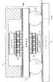
配線基板本体を構成する樹脂基板(有機基板)11の形態としては、少なくとも最外層の配線層が基板内部を通して相互に電気的に接続された形態のものであれば十分である。例えば、ビルドアップ法を用いた多層構造の配線基板を利用することができる。これは、ベース基材としてのコア基板(ガラスエポキシ基板等)を中心としてその両面に、絶縁層の形成、絶縁層におけるビアホールの形成、ビアホールの内部を含めた配線パターン(配線層)の形成を順次繰り返して積み上げていくものである。絶縁層の材料としては代表的にエポキシ樹脂が用いられ、配線層の材料としては銅(Cu)が用いられる。かかるプロセスを経て形成された最外層の配線層12,13は、基板内部の所要箇所に適宜形成された各配線層及び各配線層間を相互に接続するビアを介して電気的に接続されている。
「ロジック」チップ1を実装するためのインターポーザ20と、「メモリ」チップ2を実装するためのインターポーザ30は、サイズの違いこそあれ、基本的には同じプロセスを用いて作製することができる。
例えば、12インチの大きさのシリコンウエハに対し、その一方の面側に所要のデバイスプロセスを施して複数のデバイス(「ロジック」デバイス、又は「メモリ」デバイス)をアレイ状に作り込み、そのデバイスが形成されている側の面に窒化シリコン(SiN)やリンガラス(PSG)等からなるパッシベーション膜を形成し、各デバイス上に所要のパターンで形成されたアルミニウム(Al)の配線層の一部分に画定される電極パッドに対応する部分のパッシベーション膜をレーザ等により除去する。
先ず、「ロジック」チップ1に熱結合させるためのヒートスプレッダ3を用意する。例えば、大きさが30×30mm程度の厚めの銅板を用意し、この銅板の周囲に沿った部分を残して他の部分(中央部分)を、例えば、プレスやエッチング加工などにより、所要の深さまで凹部状に除去する。これにより、図示のようにその主要部分が板状に成形された板状部3aとその周囲に一体的に形成された側壁部3bとからなる構造体が出来上がる。さらに、この構造体の全面にニッケル(Ni)めっきを施すことで、所要のヒートスプレッダ3を得ることができる。
1a,2a…電極パッド(端子)、
3…ヒートスプレッダ(放熱部材)、
10(11)…配線基板(樹脂基板/有機基板)、
12, 13, 23,24,26,33,34,36…配線層、
12P,13P,23P,24P,26P,33P,34P,36P…パッド、
14,15,27,28,37,38…ソルダレジスト層(絶縁層/保護膜)、
16…はんだボール(外部接続端子)、
20,30…(シリコン)インターポーザ、
21,31…シリコン基板(基材)、
22,32…貫通電極、
25,35…絶縁層、
41,42,45,46…はんだバンプ(導電性部材)、
43,44,47,48…アンダーフィル樹脂、
50…インターポーザ実装配線基板(パッケージ)、
60,60a…半導体装置(電子部品装置)。
Claims (4)
- 両面に配線層を有し、該配線層が基板内部を通して相互に電気的に接続された配線基板と、
前記配線基板の一方の面側の配線層にバンプにより電気的に接続され、実装される第1の電子部品が有する熱膨張係数と同じ値もしくはこれに近似した値の熱膨張係数を有する第1のインターポーザと、
前記第1のインターポーザの前記配線基板に対向する側と反対側の面に実装された前記第1の電子部品と、
前記配線基板の他方の面側の配線層にバンプにより電気的に接続され、実装される第2の電子部品が有する熱膨張係数と同じ値もしくはこれに近似した値の熱膨張係数を有する第2のインターポーザと、
前記第2のインターポーザの前記配線基板に対向する側と反対側の面に実装された前記第2の電子部品と、
前記配線基板と、前記第1、第2のインターポーザとの間に充填されたアンダーフィル樹脂と、
前記第1の電子部品と熱的に結合され、かつ、前記第2の電子部品から熱的に遮断された放熱部材と
を備え、
前記第1の電子部品は、前記第2の電子部品と比べて動作時の発熱量が大きいデバイスであることを特徴とする電子部品装置。 - 前記第1、第2の各インターポーザは、その基材がシリコンから形成されており、前記配線基板は、その基材が樹脂から形成されていることを特徴とする請求項1に記載の電子部品装置。
- 前記第1、第2の各インターポーザは、前記配線基板を挟んで対向する位置に配設されていることを特徴とする請求項1又は2に記載の電子部品装置。
- 前記配線基板の前記第2のインターポーザが実装されている側の面に、外部接続端子が接合されていることを特徴とする請求項1乃至3のいずれか一項に記載の電子部品装置。
Priority Applications (2)
| Application Number | Priority Date | Filing Date | Title |
|---|---|---|---|
| JP2009232372A JP5330184B2 (ja) | 2009-10-06 | 2009-10-06 | 電子部品装置 |
| US12/897,082 US8379400B2 (en) | 2009-10-06 | 2010-10-04 | Interposer mounted wiring board and electronic component device |
Applications Claiming Priority (1)
| Application Number | Priority Date | Filing Date | Title |
|---|---|---|---|
| JP2009232372A JP5330184B2 (ja) | 2009-10-06 | 2009-10-06 | 電子部品装置 |
Publications (3)
| Publication Number | Publication Date |
|---|---|
| JP2011082293A JP2011082293A (ja) | 2011-04-21 |
| JP2011082293A5 JP2011082293A5 (ja) | 2012-08-16 |
| JP5330184B2 true JP5330184B2 (ja) | 2013-10-30 |
Family
ID=43823030
Family Applications (1)
| Application Number | Title | Priority Date | Filing Date |
|---|---|---|---|
| JP2009232372A Active JP5330184B2 (ja) | 2009-10-06 | 2009-10-06 | 電子部品装置 |
Country Status (2)
| Country | Link |
|---|---|
| US (1) | US8379400B2 (ja) |
| JP (1) | JP5330184B2 (ja) |
Families Citing this family (64)
| Publication number | Priority date | Publication date | Assignee | Title |
|---|---|---|---|---|
| US8557700B2 (en) | 2008-05-09 | 2013-10-15 | Invensas Corporation | Method for manufacturing a chip-size double side connection package |
| JP4998503B2 (ja) * | 2009-04-07 | 2012-08-15 | パナソニック株式会社 | 電子部品実装システムおよび電子部品実装方法 |
| US9254532B2 (en) | 2009-12-30 | 2016-02-09 | Intel Corporation | Methods of fabricating low melting point solder reinforced sealant and structures formed thereby |
| US8895380B2 (en) | 2010-11-22 | 2014-11-25 | Bridge Semiconductor Corporation | Method of making semiconductor assembly with built-in stiffener and semiconductor assembly manufactured thereby |
| KR101719636B1 (ko) * | 2011-01-28 | 2017-04-05 | 삼성전자 주식회사 | 반도체 장치 및 그 제조 방법 |
| US9627337B2 (en) * | 2011-03-31 | 2017-04-18 | Novatek Microelectronics Corp. | Integrated circuit device |
| TWI424544B (zh) * | 2011-03-31 | 2014-01-21 | 聯詠科技股份有限公司 | 積體電路裝置 |
| US8803269B2 (en) | 2011-05-05 | 2014-08-12 | Cisco Technology, Inc. | Wafer scale packaging platform for transceivers |
| US20130003336A1 (en) * | 2011-06-28 | 2013-01-03 | Delphi Technologies, Inc. | Machine placeable circuit board interposer |
| KR20130025205A (ko) * | 2011-09-01 | 2013-03-11 | 삼성전자주식회사 | 휴대용 데이터 저장 장치 |
| US8780576B2 (en) | 2011-09-14 | 2014-07-15 | Invensas Corporation | Low CTE interposer |
| JP5167516B1 (ja) * | 2011-11-30 | 2013-03-21 | 株式会社フジクラ | 部品内蔵基板及びその製造方法並びに部品内蔵基板実装体 |
| US9401308B2 (en) * | 2013-03-12 | 2016-07-26 | Taiwan Semiconductor Manufacturing Company, Ltd. | Packaging devices, methods of manufacture thereof, and packaging methods |
| US10015888B2 (en) | 2013-02-15 | 2018-07-03 | Taiwan Semiconductor Manufacturing Company, Ltd. | Interconnect joint protective layer apparatus and method |
| US9368398B2 (en) | 2012-01-12 | 2016-06-14 | Taiwan Semiconductor Manufacturing Company, Ltd. | Interconnect structure and method of fabricating same |
| US9589862B2 (en) | 2013-03-11 | 2017-03-07 | Taiwan Semiconductor Manufacturing Company, Ltd. | Interconnect structures and methods of forming same |
| US9607921B2 (en) | 2012-01-12 | 2017-03-28 | Taiwan Semiconductor Manufacturing Company, Ltd. | Package on package interconnect structure |
| US9257333B2 (en) | 2013-03-11 | 2016-02-09 | Taiwan Semiconductor Manufacturing Company, Ltd. | Interconnect structures and methods of forming same |
| US9263839B2 (en) | 2012-12-28 | 2016-02-16 | Taiwan Semiconductor Manufacturing Company, Ltd. | System and method for an improved fine pitch joint |
| JP5845105B2 (ja) * | 2012-02-17 | 2016-01-20 | キヤノン株式会社 | 電子部品の実装用基板と電子部品を実装した基板 |
| US9082776B2 (en) | 2012-08-24 | 2015-07-14 | Taiwan Semiconductor Manufacturing Company, Ltd. | Semiconductor package having protective layer with curved surface and method of manufacturing same |
| CN103050414B (zh) * | 2012-11-28 | 2016-06-29 | 贵州振华风光半导体有限公司 | 三维集成高密度厚薄膜多芯片组件的集成方法 |
| CN103107105B (zh) * | 2012-12-12 | 2015-06-24 | 贵州振华风光半导体有限公司 | 多芯片组件同质键合系统质量一致性改进方法 |
| US9312219B2 (en) * | 2012-12-28 | 2016-04-12 | Dyi-chung Hu | Interposer and packaging substrate having the interposer |
| US8884427B2 (en) | 2013-03-14 | 2014-11-11 | Invensas Corporation | Low CTE interposer without TSV structure |
| JP6196815B2 (ja) * | 2013-06-05 | 2017-09-13 | 新光電気工業株式会社 | 冷却装置及び半導体装置 |
| US20150016045A1 (en) * | 2013-07-11 | 2015-01-15 | Integrated Silicon Solution, Inc. | Memory assembly with processor matching pin-out |
| US9735082B2 (en) * | 2013-12-04 | 2017-08-15 | Taiwan Semiconductor Manufacturing Company, Ltd. | 3DIC packaging with hot spot thermal management features |
| US9318474B2 (en) * | 2013-12-16 | 2016-04-19 | Apple Inc. | Thermally enhanced wafer level fan-out POP package |
| US10431564B2 (en) | 2014-01-27 | 2019-10-01 | Mediatek Inc. | Structure and formation method of chip package structure |
| US20150262902A1 (en) | 2014-03-12 | 2015-09-17 | Invensas Corporation | Integrated circuits protected by substrates with cavities, and methods of manufacture |
| US9355997B2 (en) | 2014-03-12 | 2016-05-31 | Invensas Corporation | Integrated circuit assemblies with reinforcement frames, and methods of manufacture |
| US9165793B1 (en) | 2014-05-02 | 2015-10-20 | Invensas Corporation | Making electrical components in handle wafers of integrated circuit packages |
| US9741649B2 (en) | 2014-06-04 | 2017-08-22 | Invensas Corporation | Integrated interposer solutions for 2D and 3D IC packaging |
| US9252127B1 (en) | 2014-07-10 | 2016-02-02 | Invensas Corporation | Microelectronic assemblies with integrated circuits and interposers with cavities, and methods of manufacture |
| US9601464B2 (en) | 2014-07-10 | 2017-03-21 | Apple Inc. | Thermally enhanced package-on-package structure |
| EP3037810B1 (fr) * | 2014-12-23 | 2017-10-25 | EM Microelectronic-Marin SA | Capteur d'humidite ameliore |
| US9917026B2 (en) * | 2014-12-24 | 2018-03-13 | Renesas Electronics Corporation | Semiconductor device |
| KR101672622B1 (ko) | 2015-02-09 | 2016-11-03 | 앰코 테크놀로지 코리아 주식회사 | 반도체 디바이스 및 그 제조 방법 |
| US9478504B1 (en) | 2015-06-19 | 2016-10-25 | Invensas Corporation | Microelectronic assemblies with cavities, and methods of fabrication |
| US9859202B2 (en) * | 2015-06-24 | 2018-01-02 | Dyi-chung Hu | Spacer connector |
| CN106332499A (zh) * | 2015-06-26 | 2017-01-11 | 台达电子工业股份有限公司 | 一种用于芯片供电的组装结构、电子设备 |
| US10109593B2 (en) | 2015-07-23 | 2018-10-23 | Apple Inc. | Self shielded system in package (SiP) modules |
| US10163867B2 (en) | 2015-11-12 | 2018-12-25 | Amkor Technology, Inc. | Semiconductor package and manufacturing method thereof |
| US9892962B2 (en) | 2015-11-30 | 2018-02-13 | Taiwan Semiconductor Manufacturing Company, Ltd. | Wafer level chip scale package interconnects and methods of manufacture thereof |
| US9721903B2 (en) | 2015-12-21 | 2017-08-01 | Apple Inc. | Vertical interconnects for self shielded system in package (SiP) modules |
| EP3413349A4 (en) * | 2016-02-03 | 2019-09-11 | Shindengen Electric Manufacturing Co. Ltd. | SEMICONDUCTOR COMPONENT AND METHOD FOR PRODUCING SEMICONDUCTOR COMPONENT |
| JP6972523B2 (ja) * | 2016-09-13 | 2021-11-24 | セイコーエプソン株式会社 | 電子機器 |
| US10079194B1 (en) * | 2017-03-07 | 2018-09-18 | Novatek Microelectronics Corp. | Chip on film package |
| JP6903981B2 (ja) * | 2017-03-23 | 2021-07-14 | セイコーエプソン株式会社 | 検出装置 |
| US10181447B2 (en) | 2017-04-21 | 2019-01-15 | Invensas Corporation | 3D-interconnect |
| US10541209B2 (en) * | 2017-08-03 | 2020-01-21 | General Electric Company | Electronics package including integrated electromagnetic interference shield and method of manufacturing thereof |
| US10804115B2 (en) | 2017-08-03 | 2020-10-13 | General Electric Company | Electronics package with integrated interconnect structure and method of manufacturing thereof |
| US10541153B2 (en) * | 2017-08-03 | 2020-01-21 | General Electric Company | Electronics package with integrated interconnect structure and method of manufacturing thereof |
| US10410999B2 (en) | 2017-12-19 | 2019-09-10 | Amkor Technology, Inc. | Semiconductor device with integrated heat distribution and manufacturing method thereof |
| US20190198460A1 (en) * | 2017-12-21 | 2019-06-27 | AP Memory Technology Corp. | Circuit system having compact decoupling structure |
| US11195789B2 (en) * | 2018-11-30 | 2021-12-07 | International Business Machines Corporation | Integrated circuit module with a structurally balanced package using a bottom side interposer |
| JP7103520B2 (ja) * | 2019-06-25 | 2022-07-20 | 株式会社村田製作所 | 複合部品およびその製造方法 |
| JP7513117B2 (ja) * | 2020-12-24 | 2024-07-09 | 株式会社村田製作所 | 複合部品およびその製造方法 |
| JP7669236B2 (ja) * | 2021-09-03 | 2025-04-28 | 富士フイルム株式会社 | 半導体実装構造体 |
| US12040284B2 (en) | 2021-11-12 | 2024-07-16 | Invensas Llc | 3D-interconnect with electromagnetic interference (“EMI”) shield and/or antenna |
| CN114096078B (zh) * | 2021-11-25 | 2023-07-25 | 四川九洲电器集团有限责任公司 | 不耐高温器件的印制板保护罩制备方法、保护罩及应用 |
| US20240055311A1 (en) * | 2022-08-14 | 2024-02-15 | Taiwan Semiconductor Manufacturing Company, Ltd. | Semiconductor structure and manufacturing method thereof |
| US20250046690A1 (en) * | 2023-08-04 | 2025-02-06 | Avago Technologies International Sales Pte. Limited | Hybrid substrates and manufacturing methods thereof |
Family Cites Families (17)
| Publication number | Priority date | Publication date | Assignee | Title |
|---|---|---|---|---|
| JPH07263620A (ja) * | 1994-03-22 | 1995-10-13 | Hitachi Ltd | 半導体装置 |
| JPH10284544A (ja) * | 1997-04-10 | 1998-10-23 | Hitachi Ltd | 半導体装置およびその製造方法 |
| JP2000340736A (ja) * | 1999-05-26 | 2000-12-08 | Sony Corp | 半導体装置及びその実装構造、並びにこれらの製造方法 |
| JP2001203318A (ja) * | 1999-12-17 | 2001-07-27 | Texas Instr Inc <Ti> | 複数のフリップチップを備えた半導体アセンブリ |
| JP2002151648A (ja) * | 2000-11-07 | 2002-05-24 | Mitsubishi Electric Corp | 半導体モジュール |
| JP2002314031A (ja) * | 2001-04-13 | 2002-10-25 | Fujitsu Ltd | マルチチップモジュール |
| US6597575B1 (en) * | 2002-01-04 | 2003-07-22 | Intel Corporation | Electronic packages having good reliability comprising low modulus thermal interface materials |
| JP2004071719A (ja) | 2002-08-02 | 2004-03-04 | Sony Corp | インターポーザおよびその製造方法、並びに電子回路装置およびその製造方法 |
| JP2004079745A (ja) | 2002-08-16 | 2004-03-11 | Sony Corp | インターポーザおよびその製造方法、並びに電子回路装置およびその製造方法 |
| JP2004356619A (ja) * | 2003-03-19 | 2004-12-16 | Ngk Spark Plug Co Ltd | 中継基板、半導体素子付き中継基板、中継基板付き基板、半導体素子と中継基板と基板とからなる構造体 |
| JP4330367B2 (ja) * | 2003-04-03 | 2009-09-16 | 新光電気工業株式会社 | インターポーザー及びその製造方法ならびに電子装置 |
| JP2005167159A (ja) * | 2003-12-05 | 2005-06-23 | Toshiba Corp | 積層型半導体装置 |
| JP4205613B2 (ja) * | 2004-03-01 | 2009-01-07 | エルピーダメモリ株式会社 | 半導体装置 |
| JP4343044B2 (ja) * | 2004-06-30 | 2009-10-14 | 新光電気工業株式会社 | インターポーザ及びその製造方法並びに半導体装置 |
| JP4899406B2 (ja) * | 2005-10-12 | 2012-03-21 | 日本電気株式会社 | フリップチップ型半導体装置 |
| US7545029B2 (en) * | 2006-08-18 | 2009-06-09 | Tessera, Inc. | Stack microelectronic assemblies |
| US8018738B2 (en) * | 2008-06-02 | 2011-09-13 | Oracle America, Inc., | Voltage regulator attach for high current chip applications |
-
2009
- 2009-10-06 JP JP2009232372A patent/JP5330184B2/ja active Active
-
2010
- 2010-10-04 US US12/897,082 patent/US8379400B2/en active Active
Also Published As
| Publication number | Publication date |
|---|---|
| US20110080713A1 (en) | 2011-04-07 |
| US8379400B2 (en) | 2013-02-19 |
| JP2011082293A (ja) | 2011-04-21 |
Similar Documents
| Publication | Publication Date | Title |
|---|---|---|
| JP5330184B2 (ja) | 電子部品装置 | |
| CN100495694C (zh) | 半导体器件 | |
| US9214403B2 (en) | Stacked semiconductor package | |
| CN103094244B (zh) | 嵌埋穿孔中介层的封装基板及其制法 | |
| TWI531283B (zh) | 連接基板及層疊封裝結構 | |
| CN103515325B (zh) | 半导体封装件的制法 | |
| CN113035786A (zh) | 半导体结构及其制造方法 | |
| JP2008251912A (ja) | 半導体装置及びその製造方法 | |
| JP2011044654A (ja) | 半導体装置 | |
| CN104867908A (zh) | 倒装芯片堆叠封装 | |
| US12412869B2 (en) | Electronic structure having first and second thermal conductive materials covering conductive bumps and manufacturing method thereof, and electronic package having electronic structure and manufacturing method thereof | |
| US8957516B2 (en) | Low cost and high performance flip chip package | |
| JP2010245509A (ja) | 半導体装置 | |
| TW202217988A (zh) | 半導體裝置及製造方法 | |
| US20170025386A1 (en) | Semiconductor device | |
| JP2007242782A (ja) | 半導体装置及び電子装置 | |
| US20240194579A1 (en) | Electronic component module | |
| JP7251951B2 (ja) | 半導体装置及び半導体装置の製造方法 | |
| CN118398590B (zh) | 电子封装件及其封装基板与制法 | |
| JP4494249B2 (ja) | 半導体装置 | |
| JP4465891B2 (ja) | 半導体装置 | |
| TWI817728B (zh) | 內埋元件之封裝結構 | |
| TWI815639B (zh) | 電子封裝件及其製法 | |
| CN218827084U (zh) | 半导体封装装置 | |
| KR20200052802A (ko) | 응력 조절기를 가진 접속 회로기판 및 그의 플립 칩 조립체 |
Legal Events
| Date | Code | Title | Description |
|---|---|---|---|
| A521 | Request for written amendment filed |
Free format text: JAPANESE INTERMEDIATE CODE: A523 Effective date: 20120629 |
|
| A621 | Written request for application examination |
Free format text: JAPANESE INTERMEDIATE CODE: A621 Effective date: 20120629 |
|
| A977 | Report on retrieval |
Free format text: JAPANESE INTERMEDIATE CODE: A971007 Effective date: 20130222 |
|
| A131 | Notification of reasons for refusal |
Free format text: JAPANESE INTERMEDIATE CODE: A131 Effective date: 20130226 |
|
| A521 | Request for written amendment filed |
Free format text: JAPANESE INTERMEDIATE CODE: A523 Effective date: 20130417 |
|
| TRDD | Decision of grant or rejection written | ||
| A01 | Written decision to grant a patent or to grant a registration (utility model) |
Free format text: JAPANESE INTERMEDIATE CODE: A01 Effective date: 20130709 |
|
| A61 | First payment of annual fees (during grant procedure) |
Free format text: JAPANESE INTERMEDIATE CODE: A61 Effective date: 20130725 |
|
| R150 | Certificate of patent or registration of utility model |
Ref document number: 5330184 Country of ref document: JP Free format text: JAPANESE INTERMEDIATE CODE: R150 Free format text: JAPANESE INTERMEDIATE CODE: R150 |