JP5114130B2 - 配線基板及びその製造方法、及び半導体装置 - Google Patents
配線基板及びその製造方法、及び半導体装置 Download PDFInfo
- Publication number
- JP5114130B2 JP5114130B2 JP2007218146A JP2007218146A JP5114130B2 JP 5114130 B2 JP5114130 B2 JP 5114130B2 JP 2007218146 A JP2007218146 A JP 2007218146A JP 2007218146 A JP2007218146 A JP 2007218146A JP 5114130 B2 JP5114130 B2 JP 5114130B2
- Authority
- JP
- Japan
- Prior art keywords
- external connection
- resin
- wiring board
- layer
- wiring
- Prior art date
- Legal status (The legal status is an assumption and is not a legal conclusion. Google has not performed a legal analysis and makes no representation as to the accuracy of the status listed.)
- Active
Links
Images


Classifications
-
- H—ELECTRICITY
- H05—ELECTRIC TECHNIQUES NOT OTHERWISE PROVIDED FOR
- H05K—PRINTED CIRCUITS; CASINGS OR CONSTRUCTIONAL DETAILS OF ELECTRIC APPARATUS; MANUFACTURE OF ASSEMBLAGES OF ELECTRICAL COMPONENTS
- H05K3/00—Apparatus or processes for manufacturing printed circuits
- H05K3/22—Secondary treatment of printed circuits
- H05K3/28—Applying non-metallic protective coatings
-
- H—ELECTRICITY
- H05—ELECTRIC TECHNIQUES NOT OTHERWISE PROVIDED FOR
- H05K—PRINTED CIRCUITS; CASINGS OR CONSTRUCTIONAL DETAILS OF ELECTRIC APPARATUS; MANUFACTURE OF ASSEMBLAGES OF ELECTRICAL COMPONENTS
- H05K1/00—Printed circuits
- H05K1/02—Details
- H05K1/11—Printed elements for providing electric connections to or between printed circuits
-
- H—ELECTRICITY
- H05—ELECTRIC TECHNIQUES NOT OTHERWISE PROVIDED FOR
- H05K—PRINTED CIRCUITS; CASINGS OR CONSTRUCTIONAL DETAILS OF ELECTRIC APPARATUS; MANUFACTURE OF ASSEMBLAGES OF ELECTRICAL COMPONENTS
- H05K1/00—Printed circuits
- H05K1/02—Details
-
- H—ELECTRICITY
- H05—ELECTRIC TECHNIQUES NOT OTHERWISE PROVIDED FOR
- H05K—PRINTED CIRCUITS; CASINGS OR CONSTRUCTIONAL DETAILS OF ELECTRIC APPARATUS; MANUFACTURE OF ASSEMBLAGES OF ELECTRICAL COMPONENTS
- H05K1/00—Printed circuits
- H05K1/02—Details
- H05K1/11—Printed elements for providing electric connections to or between printed circuits
- H05K1/111—Pads for surface mounting, e.g. lay-out
- H05K1/112—Pads for surface mounting, e.g. lay-out directly combined with via connections
- H05K1/113—Via provided in pad; Pad over filled via
-
- H—ELECTRICITY
- H05—ELECTRIC TECHNIQUES NOT OTHERWISE PROVIDED FOR
- H05K—PRINTED CIRCUITS; CASINGS OR CONSTRUCTIONAL DETAILS OF ELECTRIC APPARATUS; MANUFACTURE OF ASSEMBLAGES OF ELECTRICAL COMPONENTS
- H05K2201/00—Indexing scheme relating to printed circuits covered by H05K1/00
- H05K2201/09—Shape and layout
- H05K2201/09209—Shape and layout details of conductors
- H05K2201/09372—Pads and lands
- H05K2201/09472—Recessed pad for surface mounting; Recessed electrode of component
-
- H—ELECTRICITY
- H05—ELECTRIC TECHNIQUES NOT OTHERWISE PROVIDED FOR
- H05K—PRINTED CIRCUITS; CASINGS OR CONSTRUCTIONAL DETAILS OF ELECTRIC APPARATUS; MANUFACTURE OF ASSEMBLAGES OF ELECTRICAL COMPONENTS
- H05K2203/00—Indexing scheme relating to apparatus or processes for manufacturing printed circuits covered by H05K3/00
- H05K2203/13—Moulding and encapsulation; Deposition techniques; Protective layers
- H05K2203/1305—Moulding and encapsulation
- H05K2203/1327—Moulding over PCB locally or completely
-
- H—ELECTRICITY
- H05—ELECTRIC TECHNIQUES NOT OTHERWISE PROVIDED FOR
- H05K—PRINTED CIRCUITS; CASINGS OR CONSTRUCTIONAL DETAILS OF ELECTRIC APPARATUS; MANUFACTURE OF ASSEMBLAGES OF ELECTRICAL COMPONENTS
- H05K3/00—Apparatus or processes for manufacturing printed circuits
- H05K3/10—Apparatus or processes for manufacturing printed circuits in which conductive material is applied to the insulating support in such a manner as to form the desired conductive pattern
- H05K3/20—Apparatus or processes for manufacturing printed circuits in which conductive material is applied to the insulating support in such a manner as to form the desired conductive pattern by affixing prefabricated conductor pattern
- H05K3/205—Apparatus or processes for manufacturing printed circuits in which conductive material is applied to the insulating support in such a manner as to form the desired conductive pattern by affixing prefabricated conductor pattern using a pattern electroplated or electroformed on a metallic carrier
-
- H—ELECTRICITY
- H05—ELECTRIC TECHNIQUES NOT OTHERWISE PROVIDED FOR
- H05K—PRINTED CIRCUITS; CASINGS OR CONSTRUCTIONAL DETAILS OF ELECTRIC APPARATUS; MANUFACTURE OF ASSEMBLAGES OF ELECTRICAL COMPONENTS
- H05K3/00—Apparatus or processes for manufacturing printed circuits
- H05K3/46—Manufacturing multilayer circuits
- H05K3/4644—Manufacturing multilayer circuits by building the multilayer layer by layer, i.e. build-up multilayer circuits
-
- H—ELECTRICITY
- H10—SEMICONDUCTOR DEVICES; ELECTRIC SOLID-STATE DEVICES NOT OTHERWISE PROVIDED FOR
- H10W—GENERIC PACKAGES, INTERCONNECTIONS, CONNECTORS OR OTHER CONSTRUCTIONAL DETAILS OF DEVICES COVERED BY CLASS H10
- H10W72/00—Interconnections or connectors in packages
- H10W72/90—Bond pads, in general
- H10W72/941—Dispositions of bond pads
- H10W72/9415—Dispositions of bond pads relative to the surface, e.g. recessed, protruding
-
- H—ELECTRICITY
- H10—SEMICONDUCTOR DEVICES; ELECTRIC SOLID-STATE DEVICES NOT OTHERWISE PROVIDED FOR
- H10W—GENERIC PACKAGES, INTERCONNECTIONS, CONNECTORS OR OTHER CONSTRUCTIONAL DETAILS OF DEVICES COVERED BY CLASS H10
- H10W74/00—Encapsulations, e.g. protective coatings
- H10W74/10—Encapsulations, e.g. protective coatings characterised by their shape or disposition
- H10W74/15—Encapsulations, e.g. protective coatings characterised by their shape or disposition on active surfaces of flip-chip devices, e.g. underfills
-
- H—ELECTRICITY
- H10—SEMICONDUCTOR DEVICES; ELECTRIC SOLID-STATE DEVICES NOT OTHERWISE PROVIDED FOR
- H10W—GENERIC PACKAGES, INTERCONNECTIONS, CONNECTORS OR OTHER CONSTRUCTIONAL DETAILS OF DEVICES COVERED BY CLASS H10
- H10W90/00—Package configurations
- H10W90/701—Package configurations characterised by the relative positions of pads or connectors relative to package parts
- H10W90/721—Package configurations characterised by the relative positions of pads or connectors relative to package parts of bump connectors
- H10W90/724—Package configurations characterised by the relative positions of pads or connectors relative to package parts of bump connectors between a chip and a stacked insulating package substrate, interposer or RDL
-
- H—ELECTRICITY
- H10—SEMICONDUCTOR DEVICES; ELECTRIC SOLID-STATE DEVICES NOT OTHERWISE PROVIDED FOR
- H10W—GENERIC PACKAGES, INTERCONNECTIONS, CONNECTORS OR OTHER CONSTRUCTIONAL DETAILS OF DEVICES COVERED BY CLASS H10
- H10W90/00—Package configurations
- H10W90/701—Package configurations characterised by the relative positions of pads or connectors relative to package parts
- H10W90/731—Package configurations characterised by the relative positions of pads or connectors relative to package parts of die-attach connectors
- H10W90/734—Package configurations characterised by the relative positions of pads or connectors relative to package parts of die-attach connectors between a chip and a stacked insulating package substrate, interposer or RDL
-
- Y—GENERAL TAGGING OF NEW TECHNOLOGICAL DEVELOPMENTS; GENERAL TAGGING OF CROSS-SECTIONAL TECHNOLOGIES SPANNING OVER SEVERAL SECTIONS OF THE IPC; TECHNICAL SUBJECTS COVERED BY FORMER USPC CROSS-REFERENCE ART COLLECTIONS [XRACs] AND DIGESTS
- Y10—TECHNICAL SUBJECTS COVERED BY FORMER USPC
- Y10T—TECHNICAL SUBJECTS COVERED BY FORMER US CLASSIFICATION
- Y10T29/00—Metal working
- Y10T29/49—Method of mechanical manufacture
- Y10T29/49002—Electrical device making
- Y10T29/49117—Conductor or circuit manufacturing
- Y10T29/49124—On flat or curved insulated base, e.g., printed circuit, etc.
- Y10T29/49155—Manufacturing circuit on or in base
- Y10T29/49158—Manufacturing circuit on or in base with molding of insulated base
Landscapes
- Engineering & Computer Science (AREA)
- Microelectronics & Electronic Packaging (AREA)
- Manufacturing & Machinery (AREA)
- Production Of Multi-Layered Print Wiring Board (AREA)
- Structure Of Printed Boards (AREA)
Description
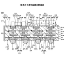
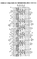
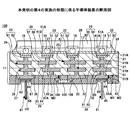
図2は、本発明の第1の実施の形態に係る半導体装置の断面図である。
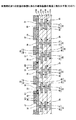
図14は、本発明の第2の実施の形態に係る半導体装置の断面図である。図14において、第1の実施の形態の半導体装置10と同一構成部分には同一符号を付す。
図15は、本発明の第3の実施の形態に係る半導体装置の断面図である。図15において、第1の実施の形態の半導体装置10と同一構成部分には同一符号を付す。
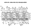
図16は、本発明の第4の実施の形態に係る半導体装置の断面図である。図16において、第2の実施の形態の半導体装置80と同一構成部分には同一符号を付す。
11,91,101 配線基板
12,13,92,105 電子部品
14,81 外部接続端子
16 バンプ
17 アンダーフィル樹脂
18,82,106 はんだ
21,27,31 樹脂層
21A,21B,27B,31B,33A,37A,51A 面
22,23 パッド
25,26,28,29 配線パターン
32,36,54,56,61,63 ビア
33,37 外部接続用パッド
41 ソルダーレジスト
41A,41B,66,67,94A,95A,95B 開口部
42 モールド樹脂
51 Au層
52 Ni層
55,57,62,64 配線
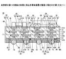
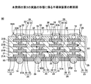
71 金属板
73 下部金型
74 上部金型
75,76 突出部
84 支持体
85 ピン本体
A 空間
B,C 突出量
D 切断位置
H1,H2 高さ
M1〜M3 厚さ
Claims (13)
- 積層されると共に、最下層又は最上層に配置された第1の樹脂層を有する複数の樹脂層と、前記複数の樹脂層に形成された配線パターンと、前記第1の樹脂層に設けられ、外部接続端子が配設される外部接続用パッドと、を備えた配線基板であって、
前記外部接続用パッドが設けられた側の前記第1の樹脂層の面に、前記外部接続用パッドを露出する開口部を有するようにモールド樹脂を設けると共に、
前記モールド樹脂の厚さを、前記外部接続用パッドに配設された前記外部接続端子よりも突出しない厚さにしたことを特徴とする配線基板。 - 積層された前記複数の樹脂層は、前記第1の樹脂層の反対側に配置された第2の樹脂層を有しており、
前記第2の樹脂層に、前記配線パターンを介して、前記外部接続用パッドと電気的に接続されると共に、電子部品が搭載される電子部品搭載用パッドを設けたことを特徴とする請求項1記載の配線基板。 - 前記外部接続端子が、はんだボール、または、ネイルヘッドとピン本体とを有するピン形状の端子であることを特徴とする請求項1または2記載の配線基板。
- 前記モールド樹脂の厚さが0.2mm〜0.3mmであることを特徴とする請求項1乃至3いずれか一項に記載の配線基板。
- 前記モールド樹脂内に電子部品が内蔵されていることを特徴とする請求項1乃至4いずれか一項に記載の配線基板。
- 前記配線基板がコアレス基板であることを特徴とする請求項1乃至5いずれか一項に記載の配線基板。
- 請求項1乃至6のうち、いずれか一項記載の配線基板と、
前記配線パターンと電気的に接続される電子部品と、を備えたことを特徴とする半導体装置。 - 積層されると共に、最下層又は最上層に配置された第1の樹脂層を有する複数の樹脂層と、前記複数の樹脂層に形成された配線パターンと、前記第1の樹脂層に設けられ、外部接続端子が配設される外部接続用パッドと、を備えた配線基板の製造方法であって、
前記最下層又は前記最上層に配置された前記第1の樹脂層の前記外部接続用パッドが設けられた側の面に、前記外部接続用パッドを露出するようにモールド樹脂を形成するモールド樹脂形成工程を、含み、
前記モールド樹脂形成工程では、前記モールド樹脂が前記外部接続用パッドに配設される前記外部接続端子よりも突出しない厚さに前記モールド樹脂を形成することを特徴とする配線基板の製造方法。 - 前記モールド樹脂は、トランスファーモールド法により形成することを特徴とする請求項8記載の配線基板の製造方法。
- 前記外部接続端子が、はんだボール、または、ネイルヘッドとピン本体とを有するピン形状の端子であることを特徴とする請求項8または9記載の配線基板の製造方法。
- 前記モールド樹脂の厚さが0.2mm〜0.3mmであることを特徴とする請求項8乃至10いずれか一項に記載の配線基板の製造方法。
- 前記モールド樹脂内に電子部品が内蔵されていることを特徴とする請求項8乃至11いずれか一項に記載の配線基板の製造方法。
- 前記配線基板がコアレス基板であることを特徴とする請求項8乃至12いずれか一項に記載の配線基板の製造方法。
Priority Applications (4)
| Application Number | Priority Date | Filing Date | Title |
|---|---|---|---|
| JP2007218146A JP5114130B2 (ja) | 2007-08-24 | 2007-08-24 | 配線基板及びその製造方法、及び半導体装置 |
| KR1020080080333A KR101412720B1 (ko) | 2007-08-24 | 2008-08-18 | 배선 기판, 그 제조 방법, 및 배선 기판을 가지는 반도체 장치 |
| TW097132053A TWI479971B (zh) | 2007-08-24 | 2008-08-22 | 佈線板,其製造方法及具有佈線板之半導體裝置 |
| US12/196,432 US8379401B2 (en) | 2007-08-24 | 2008-08-22 | Wiring board, method of manufacturing the same, and semiconductor device having wiring board |
Applications Claiming Priority (1)
| Application Number | Priority Date | Filing Date | Title |
|---|---|---|---|
| JP2007218146A JP5114130B2 (ja) | 2007-08-24 | 2007-08-24 | 配線基板及びその製造方法、及び半導体装置 |
Publications (2)
| Publication Number | Publication Date |
|---|---|
| JP2009054686A JP2009054686A (ja) | 2009-03-12 |
| JP5114130B2 true JP5114130B2 (ja) | 2013-01-09 |
Family
ID=40381945
Family Applications (1)
| Application Number | Title | Priority Date | Filing Date |
|---|---|---|---|
| JP2007218146A Active JP5114130B2 (ja) | 2007-08-24 | 2007-08-24 | 配線基板及びその製造方法、及び半導体装置 |
Country Status (4)
| Country | Link |
|---|---|
| US (1) | US8379401B2 (ja) |
| JP (1) | JP5114130B2 (ja) |
| KR (1) | KR101412720B1 (ja) |
| TW (1) | TWI479971B (ja) |
Families Citing this family (28)
| Publication number | Priority date | Publication date | Assignee | Title |
|---|---|---|---|---|
| TWI335070B (en) | 2007-03-23 | 2010-12-21 | Advanced Semiconductor Eng | Semiconductor package and the method of making the same |
| JP5290017B2 (ja) * | 2008-03-28 | 2013-09-18 | 日本特殊陶業株式会社 | 多層配線基板及びその製造方法 |
| US8217514B2 (en) * | 2008-04-07 | 2012-07-10 | Stats Chippac Ltd. | Integrated circuit packaging system with warpage control system and method of manufacture thereof |
| TWI473553B (zh) | 2008-07-03 | 2015-02-11 | 日月光半導體製造股份有限公司 | 晶片封裝結構 |
| TWI499024B (zh) | 2009-01-07 | 2015-09-01 | 日月光半導體製造股份有限公司 | 堆疊式多封裝構造裝置、半導體封裝構造及其製造方法 |
| US7851269B2 (en) * | 2009-02-19 | 2010-12-14 | Intel Corporation | Method of stiffening coreless package substrate |
| US8592691B2 (en) * | 2009-02-27 | 2013-11-26 | Ibiden Co., Ltd. | Printed wiring board |
| JP5306879B2 (ja) * | 2009-03-30 | 2013-10-02 | 日本特殊陶業株式会社 | 補強材付き配線基板 |
| US8198131B2 (en) | 2009-11-18 | 2012-06-12 | Advanced Semiconductor Engineering, Inc. | Stackable semiconductor device packages |
| TWI408785B (zh) | 2009-12-31 | 2013-09-11 | 日月光半導體製造股份有限公司 | 半導體封裝結構 |
| US8569894B2 (en) | 2010-01-13 | 2013-10-29 | Advanced Semiconductor Engineering, Inc. | Semiconductor package with single sided substrate design and manufacturing methods thereof |
| TWI419283B (zh) | 2010-02-10 | 2013-12-11 | 日月光半導體製造股份有限公司 | 封裝結構 |
| TWI411075B (zh) | 2010-03-22 | 2013-10-01 | 日月光半導體製造股份有限公司 | 半導體封裝件及其製造方法 |
| US8624374B2 (en) | 2010-04-02 | 2014-01-07 | Advanced Semiconductor Engineering, Inc. | Semiconductor device packages with fan-out and with connecting elements for stacking and manufacturing methods thereof |
| US8278746B2 (en) | 2010-04-02 | 2012-10-02 | Advanced Semiconductor Engineering, Inc. | Semiconductor device packages including connecting elements |
| TWI451546B (zh) | 2010-10-29 | 2014-09-01 | 日月光半導體製造股份有限公司 | 堆疊式封裝結構、其封裝結構及封裝結構之製造方法 |
| US9406658B2 (en) | 2010-12-17 | 2016-08-02 | Advanced Semiconductor Engineering, Inc. | Embedded component device and manufacturing methods thereof |
| JP6092117B2 (ja) * | 2010-12-24 | 2017-03-08 | エルジー イノテック カンパニー リミテッド | 印刷回路基板及びその製造方法 |
| US9171792B2 (en) | 2011-02-28 | 2015-10-27 | Advanced Semiconductor Engineering, Inc. | Semiconductor device packages having a side-by-side device arrangement and stacking functionality |
| US8952540B2 (en) * | 2011-06-30 | 2015-02-10 | Intel Corporation | In situ-built pin-grid arrays for coreless substrates, and methods of making same |
| JP2013048205A (ja) * | 2011-07-25 | 2013-03-07 | Ngk Spark Plug Co Ltd | 配線基板の製造方法 |
| US8802504B1 (en) * | 2013-03-14 | 2014-08-12 | Taiwan Semiconductor Manufacturing Company, Ltd. | 3D packages and methods for forming the same |
| US9299649B2 (en) * | 2013-02-08 | 2016-03-29 | Taiwan Semiconductor Manufacturing Company, Ltd. | 3D packages and methods for forming the same |
| JP5795415B1 (ja) * | 2014-08-29 | 2015-10-14 | 新光電気工業株式会社 | 配線基板及びその製造方法 |
| JP6319013B2 (ja) | 2014-09-24 | 2018-05-09 | 富士通株式会社 | 電子装置及び電子装置の製造方法 |
| KR102413224B1 (ko) * | 2015-10-01 | 2022-06-24 | 쑤저우 레킨 세미컨덕터 컴퍼니 리미티드 | 발광 소자, 발광 소자 제조방법 및 발광 모듈 |
| US11315862B2 (en) * | 2020-01-31 | 2022-04-26 | Taiwan Semiconductor Manufacturing Company, Ltd. | Semiconductor structure and manufacturing method thereof |
| CN115866922A (zh) * | 2021-09-24 | 2023-03-28 | 鹏鼎控股(深圳)股份有限公司 | 线路板连接结构及其制备方法 |
Family Cites Families (24)
| Publication number | Priority date | Publication date | Assignee | Title |
|---|---|---|---|---|
| US3646399A (en) * | 1970-03-04 | 1972-02-29 | Gen Electric | Printed circuit board construction |
| US5436412A (en) * | 1992-10-30 | 1995-07-25 | International Business Machines Corporation | Interconnect structure having improved metallization |
| JP2837355B2 (ja) * | 1994-09-09 | 1998-12-16 | 川崎製鉄株式会社 | 半導体icチップのパッケージ及びその製造方法並びにリード・フレーム |
| US5906042A (en) * | 1995-10-04 | 1999-05-25 | Prolinx Labs Corporation | Method and structure to interconnect traces of two conductive layers in a printed circuit board |
| JP3635219B2 (ja) * | 1999-03-11 | 2005-04-06 | 新光電気工業株式会社 | 半導体装置用多層基板及びその製造方法 |
| JP3585796B2 (ja) | 1999-12-17 | 2004-11-04 | 新光電気工業株式会社 | 多層配線基板の製造方法、及び半導体装置 |
| JP4070470B2 (ja) * | 2002-01-24 | 2008-04-02 | 新光電気工業株式会社 | 半導体装置用多層回路基板及びその製造方法並びに半導体装置 |
| US7474538B2 (en) * | 2002-05-27 | 2009-01-06 | Nec Corporation | Semiconductor device mounting board, method of manufacturing the same, method of inspecting the same, and semiconductor package |
| JP4119205B2 (ja) * | 2002-08-27 | 2008-07-16 | 富士通株式会社 | 多層配線基板 |
| JP3822549B2 (ja) * | 2002-09-26 | 2006-09-20 | 富士通株式会社 | 配線基板 |
| KR100537892B1 (ko) * | 2003-08-26 | 2005-12-21 | 삼성전자주식회사 | 칩 스택 패키지와 그 제조 방법 |
| JP4108643B2 (ja) * | 2004-05-12 | 2008-06-25 | 日本電気株式会社 | 配線基板及びそれを用いた半導体パッケージ |
| JP2005335464A (ja) * | 2004-05-25 | 2005-12-08 | Honda Motor Co Ltd | 車両の燃料供給構造 |
| JP2006041401A (ja) * | 2004-07-29 | 2006-02-09 | Sharp Corp | 半導体装置及びその製造方法 |
| JP2006093438A (ja) * | 2004-09-24 | 2006-04-06 | Denso Corp | プリント基板及びその製造方法 |
| US7626829B2 (en) * | 2004-10-27 | 2009-12-01 | Ibiden Co., Ltd. | Multilayer printed wiring board and manufacturing method of the multilayer printed wiring board |
| JP4473141B2 (ja) * | 2005-01-04 | 2010-06-02 | 日立オートモティブシステムズ株式会社 | 電子制御装置 |
| JP4072176B2 (ja) * | 2005-08-29 | 2008-04-09 | 新光電気工業株式会社 | 多層配線基板の製造方法 |
| JP4452222B2 (ja) * | 2005-09-07 | 2010-04-21 | 新光電気工業株式会社 | 多層配線基板及びその製造方法 |
| JP2007123524A (ja) * | 2005-10-27 | 2007-05-17 | Shinko Electric Ind Co Ltd | 電子部品内蔵基板 |
| CN102654409A (zh) * | 2006-04-28 | 2012-09-05 | 松下电器产业株式会社 | 电容式传感器 |
| JP4961848B2 (ja) * | 2006-06-12 | 2012-06-27 | 日本電気株式会社 | 金属ポストを有する配線基板、半導体装置及び半導体装置モジュールの製造方法 |
| DE102007034402B4 (de) * | 2006-12-14 | 2014-06-18 | Advanpack Solutions Pte. Ltd. | Halbleiterpackung und Herstellungsverfahren dafür |
| KR100827667B1 (ko) * | 2007-01-16 | 2008-05-07 | 삼성전자주식회사 | 기판 내에 반도체 칩을 갖는 반도체 패키지 및 이를제조하는 방법 |
-
2007
- 2007-08-24 JP JP2007218146A patent/JP5114130B2/ja active Active
-
2008
- 2008-08-18 KR KR1020080080333A patent/KR101412720B1/ko active Active
- 2008-08-22 TW TW097132053A patent/TWI479971B/zh active
- 2008-08-22 US US12/196,432 patent/US8379401B2/en active Active
Also Published As
| Publication number | Publication date |
|---|---|
| JP2009054686A (ja) | 2009-03-12 |
| US20090052150A1 (en) | 2009-02-26 |
| TWI479971B (zh) | 2015-04-01 |
| KR20090021076A (ko) | 2009-02-27 |
| TW200913844A (en) | 2009-03-16 |
| US8379401B2 (en) | 2013-02-19 |
| KR101412720B1 (ko) | 2014-06-26 |
Similar Documents
| Publication | Publication Date | Title |
|---|---|---|
| JP5114130B2 (ja) | 配線基板及びその製造方法、及び半導体装置 | |
| US9301391B2 (en) | Substrate structure, semiconductor package device, and manufacturing method of substrate structure | |
| JP4926692B2 (ja) | 配線基板及びその製造方法と半導体装置 | |
| JP4016039B2 (ja) | 配線基板および配線基板の製造方法 | |
| US20090135574A1 (en) | Wiring board, semiconductor device having wiring board, and method of manufacturing wiring board | |
| JP5280945B2 (ja) | 半導体装置及びその製造方法 | |
| US20100175917A1 (en) | Wiring board and method of manufacturing the same | |
| JP2006186321A (ja) | 回路基板の製造方法及び電子部品実装構造体の製造方法 | |
| JP2010283044A (ja) | 配線基板および配線基板の製造方法 | |
| JP2006049424A (ja) | 電子部品内蔵基板およびその製造方法 | |
| JP4558413B2 (ja) | 基板、半導体装置、基板の製造方法、及び半導体装置の製造方法 | |
| US20170033036A1 (en) | Printed wiring board, semiconductor package, and method for manufacturing printed wiring board | |
| JP2011249759A (ja) | 電子素子内蔵印刷回路基板及びその製造方法 | |
| KR101766476B1 (ko) | 캐비티 인쇄회로기판 제조 방법 | |
| JP5280032B2 (ja) | 配線基板 | |
| JP5357239B2 (ja) | 配線基板、半導体装置、及び配線基板の製造方法 | |
| US20170062370A1 (en) | Electronic component device | |
| JP2011014944A (ja) | 電子部品実装構造体の製造方法 | |
| JP5479638B2 (ja) | 配線基板 | |
| JP2009231635A (ja) | 配線基板及びその製造方法、及び半導体装置及びその製造方法 | |
| JP4750080B2 (ja) | 配線基板 | |
| JP2017135286A (ja) | 半導体装置及び半導体装置の製造方法 | |
| JP2005243850A (ja) | 多層プリント配線基板及びその製造方法 | |
| TW201220999A (en) | Printed circuit board and method for manufacturing the same | |
| JP4955259B2 (ja) | 配線基板、半導体装置、及び配線基板の製造方法 |
Legal Events
| Date | Code | Title | Description |
|---|---|---|---|
| A621 | Written request for application examination |
Free format text: JAPANESE INTERMEDIATE CODE: A621 Effective date: 20100531 |
|
| A977 | Report on retrieval |
Free format text: JAPANESE INTERMEDIATE CODE: A971007 Effective date: 20101118 |
|
| A131 | Notification of reasons for refusal |
Free format text: JAPANESE INTERMEDIATE CODE: A131 Effective date: 20120605 |
|
| A521 | Request for written amendment filed |
Free format text: JAPANESE INTERMEDIATE CODE: A523 Effective date: 20120802 |
|
| TRDD | Decision of grant or rejection written | ||
| A01 | Written decision to grant a patent or to grant a registration (utility model) |
Free format text: JAPANESE INTERMEDIATE CODE: A01 Effective date: 20121002 |
|
| A01 | Written decision to grant a patent or to grant a registration (utility model) |
Free format text: JAPANESE INTERMEDIATE CODE: A01 |
|
| A61 | First payment of annual fees (during grant procedure) |
Free format text: JAPANESE INTERMEDIATE CODE: A61 Effective date: 20121015 |
|
| FPAY | Renewal fee payment (event date is renewal date of database) |
Free format text: PAYMENT UNTIL: 20151019 Year of fee payment: 3 |
|
| R150 | Certificate of patent or registration of utility model |
Ref document number: 5114130 Country of ref document: JP Free format text: JAPANESE INTERMEDIATE CODE: R150 Free format text: JAPANESE INTERMEDIATE CODE: R150 |