JP2019501528A - 五置換ジシランを使用するケイ素含有フィルムの蒸着 - Google Patents
五置換ジシランを使用するケイ素含有フィルムの蒸着 Download PDFInfo
- Publication number
- JP2019501528A JP2019501528A JP2018530071A JP2018530071A JP2019501528A JP 2019501528 A JP2019501528 A JP 2019501528A JP 2018530071 A JP2018530071 A JP 2018530071A JP 2018530071 A JP2018530071 A JP 2018530071A JP 2019501528 A JP2019501528 A JP 2019501528A
- Authority
- JP
- Japan
- Prior art keywords
- silicon
- film
- forming composition
- range
- containing film
- Prior art date
- Legal status (The legal status is an assumption and is not a legal conclusion. Google has not performed a legal analysis and makes no representation as to the accuracy of the status listed.)
- Pending
Links
- 229910052710 silicon Inorganic materials 0.000 title claims abstract description 148
- 239000010703 silicon Substances 0.000 title claims abstract description 145
- XUIMIQQOPSSXEZ-UHFFFAOYSA-N Silicon Chemical group [Si] XUIMIQQOPSSXEZ-UHFFFAOYSA-N 0.000 title claims abstract description 81
- -1 pentasubstituted disilanes Chemical class 0.000 title abstract description 105
- 238000007740 vapor deposition Methods 0.000 title description 3
- 238000000034 method Methods 0.000 claims abstract description 98
- 238000000151 deposition Methods 0.000 claims abstract description 71
- 239000000758 substrate Substances 0.000 claims abstract description 70
- 239000000203 mixture Substances 0.000 claims description 188
- 239000000376 reactant Substances 0.000 claims description 67
- 229910052581 Si3N4 Inorganic materials 0.000 claims description 61
- HQVNEWCFYHHQES-UHFFFAOYSA-N silicon nitride Chemical compound N12[Si]34N5[Si]62N3[Si]51N64 HQVNEWCFYHHQES-UHFFFAOYSA-N 0.000 claims description 61
- 229910052801 chlorine Inorganic materials 0.000 claims description 56
- 229910052760 oxygen Inorganic materials 0.000 claims description 40
- 239000007789 gas Substances 0.000 claims description 37
- VYPSYNLAJGMNEJ-UHFFFAOYSA-N Silicium dioxide Chemical compound O=[Si]=O VYPSYNLAJGMNEJ-UHFFFAOYSA-N 0.000 claims description 35
- 238000006243 chemical reaction Methods 0.000 claims description 35
- 229910052814 silicon oxide Inorganic materials 0.000 claims description 33
- QVGXLLKOCUKJST-UHFFFAOYSA-N atomic oxygen Chemical compound [O] QVGXLLKOCUKJST-UHFFFAOYSA-N 0.000 claims description 29
- 239000001301 oxygen Substances 0.000 claims description 29
- 229910052799 carbon Inorganic materials 0.000 claims description 27
- 229910052757 nitrogen Inorganic materials 0.000 claims description 24
- CBENFWSGALASAD-UHFFFAOYSA-N Ozone Chemical compound [O-][O+]=O CBENFWSGALASAD-UHFFFAOYSA-N 0.000 claims description 19
- QJGQUHMNIGDVPM-UHFFFAOYSA-N nitrogen group Chemical group [N] QJGQUHMNIGDVPM-UHFFFAOYSA-N 0.000 claims description 19
- VEYJKODKHGEDMC-UHFFFAOYSA-N dichloro(trichlorosilyl)silicon Chemical compound Cl[Si](Cl)[Si](Cl)(Cl)Cl VEYJKODKHGEDMC-UHFFFAOYSA-N 0.000 claims description 18
- 229910021420 polycrystalline silicon Inorganic materials 0.000 claims description 9
- 229910021417 amorphous silicon Inorganic materials 0.000 claims description 8
- 238000002207 thermal evaporation Methods 0.000 claims 1
- RSMKAORBGALEHE-UHFFFAOYSA-N N-[dimethylamino-[tris(dimethylamino)silyl]silyl]-N-methylmethanamine Chemical compound CN(C)[SiH](N(C)C)[Si](N(C)C)(N(C)C)N(C)C RSMKAORBGALEHE-UHFFFAOYSA-N 0.000 abstract description 12
- 238000005019 vapor deposition process Methods 0.000 abstract description 3
- 239000000460 chlorine Substances 0.000 description 97
- 238000000231 atomic layer deposition Methods 0.000 description 76
- 230000008569 process Effects 0.000 description 70
- 230000008021 deposition Effects 0.000 description 61
- 239000002243 precursor Substances 0.000 description 47
- 229910052794 bromium Inorganic materials 0.000 description 40
- 229910052740 iodine Inorganic materials 0.000 description 39
- 229910052751 metal Inorganic materials 0.000 description 34
- 239000002184 metal Substances 0.000 description 34
- 229910004298 SiO 2 Inorganic materials 0.000 description 31
- 229910052739 hydrogen Inorganic materials 0.000 description 30
- 238000004833 X-ray photoelectron spectroscopy Methods 0.000 description 29
- 229910052752 metalloid Inorganic materials 0.000 description 28
- 150000002738 metalloids Chemical class 0.000 description 28
- ZMANZCXQSJIPKH-UHFFFAOYSA-N Triethylamine Chemical compound CCN(CC)CC ZMANZCXQSJIPKH-UHFFFAOYSA-N 0.000 description 27
- 238000002485 combustion reaction Methods 0.000 description 24
- 238000009826 distribution Methods 0.000 description 21
- IJGRMHOSHXDMSA-UHFFFAOYSA-N Atomic nitrogen Chemical compound N#N IJGRMHOSHXDMSA-UHFFFAOYSA-N 0.000 description 20
- 238000005229 chemical vapour deposition Methods 0.000 description 20
- 235000012431 wafers Nutrition 0.000 description 20
- 125000004178 (C1-C4) alkyl group Chemical group 0.000 description 19
- OKTJSMMVPCPJKN-UHFFFAOYSA-N Carbon Chemical compound [C] OKTJSMMVPCPJKN-UHFFFAOYSA-N 0.000 description 19
- 238000010926 purge Methods 0.000 description 19
- 239000012535 impurity Substances 0.000 description 17
- HBMJWWWQQXIZIP-UHFFFAOYSA-N silicon carbide Chemical compound [Si+]#[C-] HBMJWWWQQXIZIP-UHFFFAOYSA-N 0.000 description 15
- 229910010271 silicon carbide Inorganic materials 0.000 description 15
- 125000000217 alkyl group Chemical group 0.000 description 14
- 238000005137 deposition process Methods 0.000 description 14
- JLTRXTDYQLMHGR-UHFFFAOYSA-N trimethylaluminium Chemical compound C[Al](C)C JLTRXTDYQLMHGR-UHFFFAOYSA-N 0.000 description 14
- 239000011261 inert gas Substances 0.000 description 13
- PZKOFHKJGUNVTM-UHFFFAOYSA-N trichloro-[dichloro(trichlorosilyl)silyl]silane Chemical group Cl[Si](Cl)(Cl)[Si](Cl)(Cl)[Si](Cl)(Cl)Cl PZKOFHKJGUNVTM-UHFFFAOYSA-N 0.000 description 13
- 125000001449 isopropyl group Chemical group [H]C([H])([H])C([H])(*)C([H])([H])[H] 0.000 description 11
- 150000003254 radicals Chemical class 0.000 description 11
- 239000004065 semiconductor Substances 0.000 description 11
- QGZKDVFQNNGYKY-UHFFFAOYSA-N Ammonia Chemical group N QGZKDVFQNNGYKY-UHFFFAOYSA-N 0.000 description 10
- 150000004820 halides Chemical class 0.000 description 10
- 239000000463 material Substances 0.000 description 10
- 238000012360 testing method Methods 0.000 description 10
- 238000004519 manufacturing process Methods 0.000 description 9
- 238000000197 pyrolysis Methods 0.000 description 9
- ZAMOUSCENKQFHK-UHFFFAOYSA-N Chlorine atom Chemical compound [Cl] ZAMOUSCENKQFHK-UHFFFAOYSA-N 0.000 description 8
- 125000004429 atom Chemical group 0.000 description 8
- 239000012159 carrier gas Substances 0.000 description 8
- 150000001875 compounds Chemical class 0.000 description 8
- 239000007788 liquid Substances 0.000 description 8
- 238000000137 annealing Methods 0.000 description 7
- 239000003446 ligand Substances 0.000 description 7
- QTBSBXVTEAMEQO-UHFFFAOYSA-N Acetic acid Chemical compound CC(O)=O QTBSBXVTEAMEQO-UHFFFAOYSA-N 0.000 description 6
- XKRFYHLGVUSROY-UHFFFAOYSA-N Argon Chemical compound [Ar] XKRFYHLGVUSROY-UHFFFAOYSA-N 0.000 description 6
- RTZKZFJDLAIYFH-UHFFFAOYSA-N Diethyl ether Chemical compound CCOCC RTZKZFJDLAIYFH-UHFFFAOYSA-N 0.000 description 6
- ROSDSFDQCJNGOL-UHFFFAOYSA-N Dimethylamine Chemical compound CNC ROSDSFDQCJNGOL-UHFFFAOYSA-N 0.000 description 6
- OFBQJSOFQDEBGM-UHFFFAOYSA-N Pentane Chemical compound CCCCC OFBQJSOFQDEBGM-UHFFFAOYSA-N 0.000 description 6
- YXFVVABEGXRONW-UHFFFAOYSA-N Toluene Chemical compound CC1=CC=CC=C1 YXFVVABEGXRONW-UHFFFAOYSA-N 0.000 description 6
- DHVPLDUEYIAHOM-UHFFFAOYSA-N [SiH3][SiH](Br)Br Chemical group [SiH3][SiH](Br)Br DHVPLDUEYIAHOM-UHFFFAOYSA-N 0.000 description 6
- 150000001412 amines Chemical class 0.000 description 6
- 230000004888 barrier function Effects 0.000 description 6
- FXOCTISBMXDWGP-UHFFFAOYSA-N dichloro(silyl)silane Chemical group [SiH3][SiH](Cl)Cl FXOCTISBMXDWGP-UHFFFAOYSA-N 0.000 description 6
- SWHQGSHDNRXLCP-UHFFFAOYSA-N diiodo(silyl)silane Chemical group I[SiH]([SiH3])I SWHQGSHDNRXLCP-UHFFFAOYSA-N 0.000 description 6
- ZHQUEXQAGVKLPP-UHFFFAOYSA-N diiodosilyl(triiodo)silane Chemical group I[SiH]([Si](I)(I)I)I ZHQUEXQAGVKLPP-UHFFFAOYSA-N 0.000 description 6
- KPUWHANPEXNPJT-UHFFFAOYSA-N disiloxane Chemical class [SiH3]O[SiH3] KPUWHANPEXNPJT-UHFFFAOYSA-N 0.000 description 6
- VLKZOEOYAKHREP-UHFFFAOYSA-N n-Hexane Chemical compound CCCCCC VLKZOEOYAKHREP-UHFFFAOYSA-N 0.000 description 6
- 230000001590 oxidative effect Effects 0.000 description 6
- 125000006850 spacer group Chemical group 0.000 description 6
- LXEXBJXDGVGRAR-UHFFFAOYSA-N trichloro(trichlorosilyl)silane Chemical group Cl[Si](Cl)(Cl)[Si](Cl)(Cl)Cl LXEXBJXDGVGRAR-UHFFFAOYSA-N 0.000 description 6
- 229910021529 ammonia Inorganic materials 0.000 description 5
- 239000010432 diamond Substances 0.000 description 5
- OBUKPIPBHQGWTR-UHFFFAOYSA-N difluorosilyl(trifluoro)silane Chemical group F[SiH](F)[Si](F)(F)F OBUKPIPBHQGWTR-UHFFFAOYSA-N 0.000 description 5
- 239000001257 hydrogen Substances 0.000 description 5
- 150000004767 nitrides Chemical class 0.000 description 5
- 238000005979 thermal decomposition reaction Methods 0.000 description 5
- SCKGSKNTVOKXKZ-UHFFFAOYSA-N tribromo(dibromosilyl)silane Chemical group Br[SiH](Br)[Si](Br)(Br)Br SCKGSKNTVOKXKZ-UHFFFAOYSA-N 0.000 description 5
- 125000003903 2-propenyl group Chemical group [H]C([*])([H])C([H])=C([H])[H] 0.000 description 4
- QUSNBJAOOMFDIB-UHFFFAOYSA-N Ethylamine Chemical compound CCN QUSNBJAOOMFDIB-UHFFFAOYSA-N 0.000 description 4
- 229910052786 argon Inorganic materials 0.000 description 4
- 230000015572 biosynthetic process Effects 0.000 description 4
- 239000010949 copper Substances 0.000 description 4
- 238000000354 decomposition reaction Methods 0.000 description 4
- XBDQKXXYIPTUBI-UHFFFAOYSA-N dimethylselenoniopropionate Natural products CCC(O)=O XBDQKXXYIPTUBI-UHFFFAOYSA-N 0.000 description 4
- 238000004821 distillation Methods 0.000 description 4
- FFUAGWLWBBFQJT-UHFFFAOYSA-N hexamethyldisilazane Chemical group C[Si](C)(C)N[Si](C)(C)C FFUAGWLWBBFQJT-UHFFFAOYSA-N 0.000 description 4
- 238000011065 in-situ storage Methods 0.000 description 4
- BDAGIHXWWSANSR-UHFFFAOYSA-N methanoic acid Natural products OC=O BDAGIHXWWSANSR-UHFFFAOYSA-N 0.000 description 4
- 238000000623 plasma-assisted chemical vapour deposition Methods 0.000 description 4
- 238000001556 precipitation Methods 0.000 description 4
- 238000012545 processing Methods 0.000 description 4
- UHOVQNZJYSORNB-UHFFFAOYSA-N Benzene Chemical compound C1=CC=CC=C1 UHOVQNZJYSORNB-UHFFFAOYSA-N 0.000 description 3
- 101000871498 Homo sapiens m7GpppX diphosphatase Proteins 0.000 description 3
- UFHFLCQGNIYNRP-UHFFFAOYSA-N Hydrogen Chemical compound [H][H] UFHFLCQGNIYNRP-UHFFFAOYSA-N 0.000 description 3
- MIQYPPGTNIFAPO-CABCVRRESA-N PS(6:0/6:0) Chemical compound CCCCCC(=O)OC[C@@H](OC(=O)CCCCC)COP(O)(=O)OC[C@H](N)C(O)=O MIQYPPGTNIFAPO-CABCVRRESA-N 0.000 description 3
- CIBUDKJODXACBL-UHFFFAOYSA-N [SiH3][SiH2]Br Chemical group [SiH3][SiH2]Br CIBUDKJODXACBL-UHFFFAOYSA-N 0.000 description 3
- 238000001505 atmospheric-pressure chemical vapour deposition Methods 0.000 description 3
- 230000005587 bubbling Effects 0.000 description 3
- 239000003990 capacitor Substances 0.000 description 3
- FXMNVBZEWMANSQ-UHFFFAOYSA-N chloro(silyl)silane Chemical group [SiH3][SiH2]Cl FXMNVBZEWMANSQ-UHFFFAOYSA-N 0.000 description 3
- KOPOQZFJUQMUML-UHFFFAOYSA-N chlorosilane Chemical compound Cl[SiH3] KOPOQZFJUQMUML-UHFFFAOYSA-N 0.000 description 3
- 238000010586 diagram Methods 0.000 description 3
- 125000005265 dialkylamine group Chemical group 0.000 description 3
- ILZIHGWXTARXAO-UHFFFAOYSA-N dichloro(dichlorosilylmethyl)silane Chemical group Cl[SiH](Cl)C[SiH](Cl)Cl ILZIHGWXTARXAO-UHFFFAOYSA-N 0.000 description 3
- 239000001307 helium Substances 0.000 description 3
- 229910052734 helium Inorganic materials 0.000 description 3
- SWQJXJOGLNCZEY-UHFFFAOYSA-N helium atom Chemical compound [He] SWQJXJOGLNCZEY-UHFFFAOYSA-N 0.000 description 3
- 238000004050 hot filament vapor deposition Methods 0.000 description 3
- XUGPYSXPMMKZGO-UHFFFAOYSA-N iodo(silyl)silane Chemical group [SiH3][SiH2]I XUGPYSXPMMKZGO-UHFFFAOYSA-N 0.000 description 3
- 102100033718 m7GpppX diphosphatase Human genes 0.000 description 3
- 230000009257 reactivity Effects 0.000 description 3
- FZHAPNGMFPVSLP-UHFFFAOYSA-N silanamine Chemical compound [SiH3]N FZHAPNGMFPVSLP-UHFFFAOYSA-N 0.000 description 3
- 239000011734 sodium Substances 0.000 description 3
- 125000000999 tert-butyl group Chemical group [H]C([H])([H])C(*)(C([H])([H])[H])C([H])([H])[H] 0.000 description 3
- MSQITEWLCPTJBF-UHFFFAOYSA-N trichloro-[dichloro-[dichloro(trichlorosilyl)silyl]silyl]silane Chemical group Cl[Si](Cl)(Cl)[Si](Cl)(Cl)[Si](Cl)(Cl)[Si](Cl)(Cl)Cl MSQITEWLCPTJBF-UHFFFAOYSA-N 0.000 description 3
- APLLVYZLAPKPFW-UHFFFAOYSA-N trichloro-[dichloro-[dichloro-[dichloro(trichlorosilyl)silyl]silyl]silyl]silane Chemical group Cl[Si](Cl)(Cl)[Si](Cl)(Cl)[Si](Cl)(Cl)[Si](Cl)(Cl)[Si](Cl)(Cl)Cl APLLVYZLAPKPFW-UHFFFAOYSA-N 0.000 description 3
- CIEKVFFSPFYSHN-UHFFFAOYSA-N triiodo(triiodosilyl)silane Chemical group I[Si](I)(I)[Si](I)(I)I CIEKVFFSPFYSHN-UHFFFAOYSA-N 0.000 description 3
- 239000012808 vapor phase Substances 0.000 description 3
- HBEDSQVIWPRPAY-UHFFFAOYSA-N 2,3-dihydrobenzofuran Chemical compound C1=CC=C2OCCC2=C1 HBEDSQVIWPRPAY-UHFFFAOYSA-N 0.000 description 2
- OSWFIVFLDKOXQC-UHFFFAOYSA-N 4-(3-methoxyphenyl)aniline Chemical compound COC1=CC=CC(C=2C=CC(N)=CC=2)=C1 OSWFIVFLDKOXQC-UHFFFAOYSA-N 0.000 description 2
- ZCYVEMRRCGMTRW-UHFFFAOYSA-N 7553-56-2 Chemical compound [I] ZCYVEMRRCGMTRW-UHFFFAOYSA-N 0.000 description 2
- 239000005046 Chlorosilane Substances 0.000 description 2
- IMNFDUFMRHMDMM-UHFFFAOYSA-N N-Heptane Chemical compound CCCCCCC IMNFDUFMRHMDMM-UHFFFAOYSA-N 0.000 description 2
- KDLHZDBZIXYQEI-UHFFFAOYSA-N Palladium Chemical compound [Pd] KDLHZDBZIXYQEI-UHFFFAOYSA-N 0.000 description 2
- 235000011054 acetic acid Nutrition 0.000 description 2
- 125000001931 aliphatic group Chemical group 0.000 description 2
- 229910052782 aluminium Inorganic materials 0.000 description 2
- 238000004458 analytical method Methods 0.000 description 2
- 238000000998 batch distillation Methods 0.000 description 2
- 230000009286 beneficial effect Effects 0.000 description 2
- 230000033228 biological regulation Effects 0.000 description 2
- 125000000484 butyl group Chemical group [H]C([*])([H])C([H])([H])C([H])([H])C([H])([H])[H] 0.000 description 2
- 150000001735 carboxylic acids Chemical class 0.000 description 2
- 239000003054 catalyst Substances 0.000 description 2
- VWBWKXZFNDNPLX-UHFFFAOYSA-N chloro(ethylsilylsilyl)silane Chemical group Cl[SiH2][SiH2][SiH2]CC VWBWKXZFNDNPLX-UHFFFAOYSA-N 0.000 description 2
- SLLGVCUQYRMELA-UHFFFAOYSA-N chlorosilicon Chemical group Cl[Si] SLLGVCUQYRMELA-UHFFFAOYSA-N 0.000 description 2
- 230000000052 comparative effect Effects 0.000 description 2
- 239000000356 contaminant Substances 0.000 description 2
- 238000011109 contamination Methods 0.000 description 2
- 125000006165 cyclic alkyl group Chemical group 0.000 description 2
- 125000004122 cyclic group Chemical group 0.000 description 2
- RUSXXJKVMARGOF-UHFFFAOYSA-N cyclohexane;heptane Chemical compound C1CCCCC1.CCCCCCC RUSXXJKVMARGOF-UHFFFAOYSA-N 0.000 description 2
- DIOQZVSQGTUSAI-UHFFFAOYSA-N decane Chemical compound CCCCCCCCCC DIOQZVSQGTUSAI-UHFFFAOYSA-N 0.000 description 2
- 230000007423 decrease Effects 0.000 description 2
- 239000003989 dielectric material Substances 0.000 description 2
- PZPGRFITIJYNEJ-UHFFFAOYSA-N disilane Chemical class [SiH3][SiH3] PZPGRFITIJYNEJ-UHFFFAOYSA-N 0.000 description 2
- SNRUBQQJIBEYMU-UHFFFAOYSA-N dodecane Chemical compound CCCCCCCCCCCC SNRUBQQJIBEYMU-UHFFFAOYSA-N 0.000 description 2
- 230000009977 dual effect Effects 0.000 description 2
- 125000001495 ethyl group Chemical group [H]C([H])([H])C([H])([H])* 0.000 description 2
- 238000001704 evaporation Methods 0.000 description 2
- 230000008020 evaporation Effects 0.000 description 2
- 235000019253 formic acid Nutrition 0.000 description 2
- 238000010438 heat treatment Methods 0.000 description 2
- 150000002431 hydrogen Chemical class 0.000 description 2
- 239000011630 iodine Substances 0.000 description 2
- HSZCZNFXUDYRKD-UHFFFAOYSA-M lithium iodide Chemical compound [Li+].[I-] HSZCZNFXUDYRKD-UHFFFAOYSA-M 0.000 description 2
- 238000004518 low pressure chemical vapour deposition Methods 0.000 description 2
- WPBNNNQJVZRUHP-UHFFFAOYSA-L manganese(2+);methyl n-[[2-(methoxycarbonylcarbamothioylamino)phenyl]carbamothioyl]carbamate;n-[2-(sulfidocarbothioylamino)ethyl]carbamodithioate Chemical compound [Mn+2].[S-]C(=S)NCCNC([S-])=S.COC(=O)NC(=S)NC1=CC=CC=C1NC(=S)NC(=O)OC WPBNNNQJVZRUHP-UHFFFAOYSA-L 0.000 description 2
- 238000005259 measurement Methods 0.000 description 2
- 125000002496 methyl group Chemical group [H]C([H])([H])* 0.000 description 2
- OWKFQWAGPHVFRF-UHFFFAOYSA-N n-(diethylaminosilyl)-n-ethylethanamine Chemical group CCN(CC)[SiH2]N(CC)CC OWKFQWAGPHVFRF-UHFFFAOYSA-N 0.000 description 2
- NGBPGLNJSMULPS-UHFFFAOYSA-N n-[[chloro-bis(dimethylamino)silyl]-bis(dimethylamino)silyl]-n-methylmethanamine Chemical compound CN(C)[Si](Cl)(N(C)C)[Si](N(C)C)(N(C)C)N(C)C NGBPGLNJSMULPS-UHFFFAOYSA-N 0.000 description 2
- 238000005457 optimization Methods 0.000 description 2
- 239000007800 oxidant agent Substances 0.000 description 2
- 238000000059 patterning Methods 0.000 description 2
- 238000009832 plasma treatment Methods 0.000 description 2
- BASFCYQUMIYNBI-UHFFFAOYSA-N platinum Chemical compound [Pt] BASFCYQUMIYNBI-UHFFFAOYSA-N 0.000 description 2
- 235000019260 propionic acid Nutrition 0.000 description 2
- 125000001436 propyl group Chemical group [H]C([*])([H])C([H])([H])C([H])([H])[H] 0.000 description 2
- IUVKMZGDUIUOCP-BTNSXGMBSA-N quinbolone Chemical compound O([C@H]1CC[C@H]2[C@H]3[C@@H]([C@]4(C=CC(=O)C=C4CC3)C)CC[C@@]21C)C1=CCCC1 IUVKMZGDUIUOCP-BTNSXGMBSA-N 0.000 description 2
- 229910000077 silane Inorganic materials 0.000 description 2
- 150000004756 silanes Chemical class 0.000 description 2
- LIVNPJMFVYWSIS-UHFFFAOYSA-N silicon monoxide Chemical compound [Si-]#[O+] LIVNPJMFVYWSIS-UHFFFAOYSA-N 0.000 description 2
- 239000007787 solid Substances 0.000 description 2
- 239000002904 solvent Substances 0.000 description 2
- VOITXYVAKOUIBA-UHFFFAOYSA-N triethylaluminium Chemical compound CC[Al](CC)CC VOITXYVAKOUIBA-UHFFFAOYSA-N 0.000 description 2
- LALRXNPLTWZJIJ-UHFFFAOYSA-N triethylborane Chemical compound CCB(CC)CC LALRXNPLTWZJIJ-UHFFFAOYSA-N 0.000 description 2
- WXRGABKACDFXMG-UHFFFAOYSA-N trimethylborane Chemical compound CB(C)C WXRGABKACDFXMG-UHFFFAOYSA-N 0.000 description 2
- XCZXGTMEAKBVPV-UHFFFAOYSA-N trimethylgallium Chemical compound C[Ga](C)C XCZXGTMEAKBVPV-UHFFFAOYSA-N 0.000 description 2
- GIRKRMUMWJFNRI-UHFFFAOYSA-N tris(dimethylamino)silicon Chemical group CN(C)[Si](N(C)C)N(C)C GIRKRMUMWJFNRI-UHFFFAOYSA-N 0.000 description 2
- VEDJZFSRVVQBIL-UHFFFAOYSA-N trisilane Chemical compound [SiH3][SiH2][SiH3] VEDJZFSRVVQBIL-UHFFFAOYSA-N 0.000 description 2
- XLYOFNOQVPJJNP-UHFFFAOYSA-N water Substances O XLYOFNOQVPJJNP-UHFFFAOYSA-N 0.000 description 2
- 239000010963 304 stainless steel Substances 0.000 description 1
- AMKGKYQBASDDJB-UHFFFAOYSA-N 9$l^{2}-borabicyclo[3.3.1]nonane Chemical compound C1CCC2CCCC1[B]2 AMKGKYQBASDDJB-UHFFFAOYSA-N 0.000 description 1
- WKBOTKDWSSQWDR-UHFFFAOYSA-N Bromine atom Chemical compound [Br] WKBOTKDWSSQWDR-UHFFFAOYSA-N 0.000 description 1
- 239000004215 Carbon black (E152) Substances 0.000 description 1
- 229910052684 Cerium Inorganic materials 0.000 description 1
- RYGMFSIKBFXOCR-UHFFFAOYSA-N Copper Chemical compound [Cu] RYGMFSIKBFXOCR-UHFFFAOYSA-N 0.000 description 1
- XDTMQSROBMDMFD-UHFFFAOYSA-N Cyclohexane Chemical compound C1CCCCC1 XDTMQSROBMDMFD-UHFFFAOYSA-N 0.000 description 1
- 229910052692 Dysprosium Inorganic materials 0.000 description 1
- 229910052691 Erbium Inorganic materials 0.000 description 1
- 229910052688 Gadolinium Inorganic materials 0.000 description 1
- 229910001218 Gallium arsenide Inorganic materials 0.000 description 1
- DGAQECJNVWCQMB-PUAWFVPOSA-M Ilexoside XXIX Chemical compound C[C@@H]1CC[C@@]2(CC[C@@]3(C(=CC[C@H]4[C@]3(CC[C@@H]5[C@@]4(CC[C@@H](C5(C)C)OS(=O)(=O)[O-])C)C)[C@@H]2[C@]1(C)O)C)C(=O)O[C@H]6[C@@H]([C@H]([C@@H]([C@H](O6)CO)O)O)O.[Na+] DGAQECJNVWCQMB-PUAWFVPOSA-M 0.000 description 1
- FYYHWMGAXLPEAU-UHFFFAOYSA-N Magnesium Chemical compound [Mg] FYYHWMGAXLPEAU-UHFFFAOYSA-N 0.000 description 1
- CTQNGGLPUBDAKN-UHFFFAOYSA-N O-Xylene Chemical compound CC1=CC=CC=C1C CTQNGGLPUBDAKN-UHFFFAOYSA-N 0.000 description 1
- 229920000144 PEDOT:PSS Polymers 0.000 description 1
- 229920001609 Poly(3,4-ethylenedioxythiophene) Polymers 0.000 description 1
- ZLMJMSJWJFRBEC-UHFFFAOYSA-N Potassium Chemical compound [K] ZLMJMSJWJFRBEC-UHFFFAOYSA-N 0.000 description 1
- 229910052777 Praseodymium Inorganic materials 0.000 description 1
- YZCKVEUIGOORGS-IGMARMGPSA-N Protium Chemical compound [1H] YZCKVEUIGOORGS-IGMARMGPSA-N 0.000 description 1
- KJTLSVCANCCWHF-UHFFFAOYSA-N Ruthenium Chemical compound [Ru] KJTLSVCANCCWHF-UHFFFAOYSA-N 0.000 description 1
- 229910000589 SAE 304 stainless steel Inorganic materials 0.000 description 1
- RTAQQCXQSZGOHL-UHFFFAOYSA-N Titanium Chemical compound [Ti] RTAQQCXQSZGOHL-UHFFFAOYSA-N 0.000 description 1
- 238000003848 UV Light-Curing Methods 0.000 description 1
- 229910052769 Ytterbium Inorganic materials 0.000 description 1
- 230000002378 acidificating effect Effects 0.000 description 1
- 239000000443 aerosol Substances 0.000 description 1
- 150000003973 alkyl amines Chemical class 0.000 description 1
- XAGFODPZIPBFFR-UHFFFAOYSA-N aluminium Chemical compound [Al] XAGFODPZIPBFFR-UHFFFAOYSA-N 0.000 description 1
- 229910052785 arsenic Inorganic materials 0.000 description 1
- 230000008901 benefit Effects 0.000 description 1
- 229910052797 bismuth Inorganic materials 0.000 description 1
- JCXGWMGPZLAOME-UHFFFAOYSA-N bismuth atom Chemical compound [Bi] JCXGWMGPZLAOME-UHFFFAOYSA-N 0.000 description 1
- GDTBXPJZTBHREO-UHFFFAOYSA-N bromine Substances BrBr GDTBXPJZTBHREO-UHFFFAOYSA-N 0.000 description 1
- 239000006227 byproduct Substances 0.000 description 1
- 229910002091 carbon monoxide Inorganic materials 0.000 description 1
- 150000001768 cations Chemical class 0.000 description 1
- ZMIGMASIKSOYAM-UHFFFAOYSA-N cerium Chemical compound [Ce][Ce][Ce][Ce][Ce][Ce][Ce][Ce][Ce][Ce][Ce][Ce][Ce][Ce][Ce][Ce][Ce][Ce][Ce][Ce][Ce][Ce][Ce][Ce][Ce][Ce][Ce][Ce][Ce][Ce][Ce][Ce][Ce][Ce][Ce][Ce][Ce][Ce] ZMIGMASIKSOYAM-UHFFFAOYSA-N 0.000 description 1
- 229910052802 copper Inorganic materials 0.000 description 1
- 238000005260 corrosion Methods 0.000 description 1
- 230000007797 corrosion Effects 0.000 description 1
- 125000000113 cyclohexyl group Chemical group [H]C1([H])C([H])([H])C([H])([H])C([H])(*)C([H])([H])C1([H])[H] 0.000 description 1
- 125000001511 cyclopentyl group Chemical group [H]C1([H])C([H])([H])C([H])([H])C([H])(*)C1([H])[H] 0.000 description 1
- 125000001559 cyclopropyl group Chemical group [H]C1([H])C([H])([H])C1([H])* 0.000 description 1
- 238000011161 development Methods 0.000 description 1
- 229910003460 diamond Inorganic materials 0.000 description 1
- CEJLBZWIKQJOAT-UHFFFAOYSA-N dichloroisocyanuric acid Chemical compound ClN1C(=O)NC(=O)N(Cl)C1=O CEJLBZWIKQJOAT-UHFFFAOYSA-N 0.000 description 1
- HQWPLXHWEZZGKY-UHFFFAOYSA-N diethylzinc Chemical compound CC[Zn]CC HQWPLXHWEZZGKY-UHFFFAOYSA-N 0.000 description 1
- 125000002147 dimethylamino group Chemical group [H]C([H])([H])N(*)C([H])([H])[H] 0.000 description 1
- AXAZMDOAUQTMOW-UHFFFAOYSA-N dimethylzinc Chemical compound C[Zn]C AXAZMDOAUQTMOW-UHFFFAOYSA-N 0.000 description 1
- 239000002019 doping agent Substances 0.000 description 1
- 238000001035 drying Methods 0.000 description 1
- KBQHZAAAGSGFKK-UHFFFAOYSA-N dysprosium atom Chemical compound [Dy] KBQHZAAAGSGFKK-UHFFFAOYSA-N 0.000 description 1
- 230000000694 effects Effects 0.000 description 1
- 238000001227 electron beam curing Methods 0.000 description 1
- 238000005538 encapsulation Methods 0.000 description 1
- 238000005516 engineering process Methods 0.000 description 1
- UYAHIZSMUZPPFV-UHFFFAOYSA-N erbium Chemical compound [Er] UYAHIZSMUZPPFV-UHFFFAOYSA-N 0.000 description 1
- 238000011156 evaluation Methods 0.000 description 1
- 238000002474 experimental method Methods 0.000 description 1
- 239000012530 fluid Substances 0.000 description 1
- 125000000524 functional group Chemical group 0.000 description 1
- UIWYJDYFSGRHKR-UHFFFAOYSA-N gadolinium atom Chemical compound [Gd] UIWYJDYFSGRHKR-UHFFFAOYSA-N 0.000 description 1
- 229910052732 germanium Inorganic materials 0.000 description 1
- GNPVGFCGXDBREM-UHFFFAOYSA-N germanium atom Chemical compound [Ge] GNPVGFCGXDBREM-UHFFFAOYSA-N 0.000 description 1
- 239000011521 glass Substances 0.000 description 1
- PCHJSUWPFVWCPO-UHFFFAOYSA-N gold Chemical compound [Au] PCHJSUWPFVWCPO-UHFFFAOYSA-N 0.000 description 1
- 229910052737 gold Inorganic materials 0.000 description 1
- 239000010931 gold Substances 0.000 description 1
- 229910052736 halogen Inorganic materials 0.000 description 1
- 125000005843 halogen group Chemical group 0.000 description 1
- 229910000856 hastalloy Inorganic materials 0.000 description 1
- SPRIOUNJHPCKPV-UHFFFAOYSA-N hydridoaluminium Chemical compound [AlH] SPRIOUNJHPCKPV-UHFFFAOYSA-N 0.000 description 1
- 229930195733 hydrocarbon Natural products 0.000 description 1
- 150000002430 hydrocarbons Chemical class 0.000 description 1
- 125000004435 hydrogen atom Chemical group [H]* 0.000 description 1
- 229910001026 inconel Inorganic materials 0.000 description 1
- 238000009616 inductively coupled plasma Methods 0.000 description 1
- 238000002347 injection Methods 0.000 description 1
- 239000007924 injection Substances 0.000 description 1
- IDIOJRGTRFRIJL-UHFFFAOYSA-N iodosilane Chemical compound I[SiH3] IDIOJRGTRFRIJL-UHFFFAOYSA-N 0.000 description 1
- BUZRAOJSFRKWPD-UHFFFAOYSA-N isocyanatosilane Chemical class [SiH3]N=C=O BUZRAOJSFRKWPD-UHFFFAOYSA-N 0.000 description 1
- 238000002955 isolation Methods 0.000 description 1
- 229910052747 lanthanoid Inorganic materials 0.000 description 1
- 150000002602 lanthanoids Chemical class 0.000 description 1
- 229910052746 lanthanum Inorganic materials 0.000 description 1
- FZLIPJUXYLNCLC-UHFFFAOYSA-N lanthanum atom Chemical compound [La] FZLIPJUXYLNCLC-UHFFFAOYSA-N 0.000 description 1
- 239000007791 liquid phase Substances 0.000 description 1
- 239000012280 lithium aluminium hydride Substances 0.000 description 1
- 238000011068 loading method Methods 0.000 description 1
- 229910052749 magnesium Inorganic materials 0.000 description 1
- 239000011777 magnesium Substances 0.000 description 1
- 239000011572 manganese Substances 0.000 description 1
- AUHZEENZYGFFBQ-UHFFFAOYSA-N mesitylene Substances CC1=CC(C)=CC(C)=C1 AUHZEENZYGFFBQ-UHFFFAOYSA-N 0.000 description 1
- 125000001827 mesitylenyl group Chemical group [H]C1=C(C(*)=C(C([H])=C1C([H])([H])[H])C([H])([H])[H])C([H])([H])[H] 0.000 description 1
- 150000002739 metals Chemical class 0.000 description 1
- FCFRXVHQYCYAOT-UHFFFAOYSA-N n-[bis(dimethylamino)-[tris(dimethylamino)silyl]silyl]-n-methylmethanamine Chemical compound CN(C)[Si](N(C)C)(N(C)C)[Si](N(C)C)(N(C)C)N(C)C FCFRXVHQYCYAOT-UHFFFAOYSA-N 0.000 description 1
- 229910000510 noble metal Inorganic materials 0.000 description 1
- 239000003960 organic solvent Substances 0.000 description 1
- 238000010422 painting Methods 0.000 description 1
- 229910052763 palladium Inorganic materials 0.000 description 1
- 230000000737 periodic effect Effects 0.000 description 1
- HKOOXMFOFWEVGF-UHFFFAOYSA-N phenylhydrazine Chemical compound NNC1=CC=CC=C1 HKOOXMFOFWEVGF-UHFFFAOYSA-N 0.000 description 1
- 229940067157 phenylhydrazine Drugs 0.000 description 1
- PARWUHTVGZSQPD-UHFFFAOYSA-N phenylsilane Chemical compound [SiH3]C1=CC=CC=C1 PARWUHTVGZSQPD-UHFFFAOYSA-N 0.000 description 1
- 229910052698 phosphorus Inorganic materials 0.000 description 1
- 229920003023 plastic Polymers 0.000 description 1
- 229910052697 platinum Inorganic materials 0.000 description 1
- 229920001467 poly(styrenesulfonates) Polymers 0.000 description 1
- 229920005591 polysilicon Polymers 0.000 description 1
- 229910052700 potassium Inorganic materials 0.000 description 1
- 239000011591 potassium Substances 0.000 description 1
- PUDIUYLPXJFUGB-UHFFFAOYSA-N praseodymium atom Chemical compound [Pr] PUDIUYLPXJFUGB-UHFFFAOYSA-N 0.000 description 1
- 239000002244 precipitate Substances 0.000 description 1
- DNXIASIHZYFFRO-UHFFFAOYSA-N pyrazoline Chemical compound C1CN=NC1 DNXIASIHZYFFRO-UHFFFAOYSA-N 0.000 description 1
- 238000004151 rapid thermal annealing Methods 0.000 description 1
- 230000009467 reduction Effects 0.000 description 1
- 239000011819 refractory material Substances 0.000 description 1
- 229910052703 rhodium Inorganic materials 0.000 description 1
- 239000010948 rhodium Substances 0.000 description 1
- MHOVAHRLVXNVSD-UHFFFAOYSA-N rhodium atom Chemical compound [Rh] MHOVAHRLVXNVSD-UHFFFAOYSA-N 0.000 description 1
- 229910052707 ruthenium Inorganic materials 0.000 description 1
- 238000001878 scanning electron micrograph Methods 0.000 description 1
- 125000002914 sec-butyl group Chemical group [H]C([H])([H])C([H])([H])C([H])(*)C([H])([H])[H] 0.000 description 1
- 150000003376 silicon Chemical class 0.000 description 1
- SBEQWOXEGHQIMW-UHFFFAOYSA-N silicon Chemical compound [Si].[Si] SBEQWOXEGHQIMW-UHFFFAOYSA-N 0.000 description 1
- 239000000377 silicon dioxide Substances 0.000 description 1
- 239000002210 silicon-based material Substances 0.000 description 1
- 229910052708 sodium Inorganic materials 0.000 description 1
- 239000012279 sodium borohydride Substances 0.000 description 1
- 229910000033 sodium borohydride Inorganic materials 0.000 description 1
- 239000007790 solid phase Substances 0.000 description 1
- 239000000243 solution Substances 0.000 description 1
- 238000001179 sorption measurement Methods 0.000 description 1
- 239000010421 standard material Substances 0.000 description 1
- 239000000126 substance Substances 0.000 description 1
- 238000003786 synthesis reaction Methods 0.000 description 1
- 230000002194 synthesizing effect Effects 0.000 description 1
- UVVUGWBBCDFNSD-UHFFFAOYSA-N tetraisocyanatosilane Chemical compound O=C=N[Si](N=C=O)(N=C=O)N=C=O UVVUGWBBCDFNSD-UHFFFAOYSA-N 0.000 description 1
- 238000002230 thermal chemical vapour deposition Methods 0.000 description 1
- 229910052719 titanium Inorganic materials 0.000 description 1
- 239000010936 titanium Substances 0.000 description 1
- ABDDAHLAEXNYRC-UHFFFAOYSA-N trichloro(trichlorosilylmethyl)silane Chemical group Cl[Si](Cl)(Cl)C[Si](Cl)(Cl)Cl ABDDAHLAEXNYRC-UHFFFAOYSA-N 0.000 description 1
- ZDHXKXAHOVTTAH-UHFFFAOYSA-N trichlorosilane Chemical compound Cl[SiH](Cl)Cl ZDHXKXAHOVTTAH-UHFFFAOYSA-N 0.000 description 1
- 239000005052 trichlorosilane Substances 0.000 description 1
- WFKWXMTUELFFGS-UHFFFAOYSA-N tungsten Chemical compound [W] WFKWXMTUELFFGS-UHFFFAOYSA-N 0.000 description 1
- 229910052721 tungsten Inorganic materials 0.000 description 1
- 239000010937 tungsten Substances 0.000 description 1
- 238000003466 welding Methods 0.000 description 1
- 239000008096 xylene Substances 0.000 description 1
- NAWDYIZEMPQZHO-UHFFFAOYSA-N ytterbium Chemical compound [Yb] NAWDYIZEMPQZHO-UHFFFAOYSA-N 0.000 description 1
- 229910052727 yttrium Inorganic materials 0.000 description 1
- VWQVUPCCIRVNHF-UHFFFAOYSA-N yttrium atom Chemical compound [Y] VWQVUPCCIRVNHF-UHFFFAOYSA-N 0.000 description 1
Images


Classifications
-
- H—ELECTRICITY
- H01—ELECTRIC ELEMENTS
- H01L—SEMICONDUCTOR DEVICES NOT COVERED BY CLASS H10
- H01L21/00—Processes or apparatus adapted for the manufacture or treatment of semiconductor or solid state devices or of parts thereof
- H01L21/02—Manufacture or treatment of semiconductor devices or of parts thereof
- H01L21/02104—Forming layers
- H01L21/02107—Forming insulating materials on a substrate
- H01L21/02225—Forming insulating materials on a substrate characterised by the process for the formation of the insulating layer
- H01L21/0226—Forming insulating materials on a substrate characterised by the process for the formation of the insulating layer formation by a deposition process
- H01L21/02263—Forming insulating materials on a substrate characterised by the process for the formation of the insulating layer formation by a deposition process deposition from the gas or vapour phase
- H01L21/02271—Forming insulating materials on a substrate characterised by the process for the formation of the insulating layer formation by a deposition process deposition from the gas or vapour phase deposition by decomposition or reaction of gaseous or vapour phase compounds, i.e. chemical vapour deposition
- H01L21/0228—Forming insulating materials on a substrate characterised by the process for the formation of the insulating layer formation by a deposition process deposition from the gas or vapour phase deposition by decomposition or reaction of gaseous or vapour phase compounds, i.e. chemical vapour deposition deposition by cyclic CVD, e.g. ALD, ALE, pulsed CVD
-
- C—CHEMISTRY; METALLURGY
- C23—COATING METALLIC MATERIAL; COATING MATERIAL WITH METALLIC MATERIAL; CHEMICAL SURFACE TREATMENT; DIFFUSION TREATMENT OF METALLIC MATERIAL; COATING BY VACUUM EVAPORATION, BY SPUTTERING, BY ION IMPLANTATION OR BY CHEMICAL VAPOUR DEPOSITION, IN GENERAL; INHIBITING CORROSION OF METALLIC MATERIAL OR INCRUSTATION IN GENERAL
- C23C—COATING METALLIC MATERIAL; COATING MATERIAL WITH METALLIC MATERIAL; SURFACE TREATMENT OF METALLIC MATERIAL BY DIFFUSION INTO THE SURFACE, BY CHEMICAL CONVERSION OR SUBSTITUTION; COATING BY VACUUM EVAPORATION, BY SPUTTERING, BY ION IMPLANTATION OR BY CHEMICAL VAPOUR DEPOSITION, IN GENERAL
- C23C16/00—Chemical coating by decomposition of gaseous compounds, without leaving reaction products of surface material in the coating, i.e. chemical vapour deposition [CVD] processes
- C23C16/22—Chemical coating by decomposition of gaseous compounds, without leaving reaction products of surface material in the coating, i.e. chemical vapour deposition [CVD] processes characterised by the deposition of inorganic material, other than metallic material
- C23C16/24—Deposition of silicon only
-
- C—CHEMISTRY; METALLURGY
- C23—COATING METALLIC MATERIAL; COATING MATERIAL WITH METALLIC MATERIAL; CHEMICAL SURFACE TREATMENT; DIFFUSION TREATMENT OF METALLIC MATERIAL; COATING BY VACUUM EVAPORATION, BY SPUTTERING, BY ION IMPLANTATION OR BY CHEMICAL VAPOUR DEPOSITION, IN GENERAL; INHIBITING CORROSION OF METALLIC MATERIAL OR INCRUSTATION IN GENERAL
- C23C—COATING METALLIC MATERIAL; COATING MATERIAL WITH METALLIC MATERIAL; SURFACE TREATMENT OF METALLIC MATERIAL BY DIFFUSION INTO THE SURFACE, BY CHEMICAL CONVERSION OR SUBSTITUTION; COATING BY VACUUM EVAPORATION, BY SPUTTERING, BY ION IMPLANTATION OR BY CHEMICAL VAPOUR DEPOSITION, IN GENERAL
- C23C16/00—Chemical coating by decomposition of gaseous compounds, without leaving reaction products of surface material in the coating, i.e. chemical vapour deposition [CVD] processes
- C23C16/22—Chemical coating by decomposition of gaseous compounds, without leaving reaction products of surface material in the coating, i.e. chemical vapour deposition [CVD] processes characterised by the deposition of inorganic material, other than metallic material
- C23C16/30—Deposition of compounds, mixtures or solid solutions, e.g. borides, carbides, nitrides
- C23C16/32—Carbides
- C23C16/325—Silicon carbide
-
- C—CHEMISTRY; METALLURGY
- C23—COATING METALLIC MATERIAL; COATING MATERIAL WITH METALLIC MATERIAL; CHEMICAL SURFACE TREATMENT; DIFFUSION TREATMENT OF METALLIC MATERIAL; COATING BY VACUUM EVAPORATION, BY SPUTTERING, BY ION IMPLANTATION OR BY CHEMICAL VAPOUR DEPOSITION, IN GENERAL; INHIBITING CORROSION OF METALLIC MATERIAL OR INCRUSTATION IN GENERAL
- C23C—COATING METALLIC MATERIAL; COATING MATERIAL WITH METALLIC MATERIAL; SURFACE TREATMENT OF METALLIC MATERIAL BY DIFFUSION INTO THE SURFACE, BY CHEMICAL CONVERSION OR SUBSTITUTION; COATING BY VACUUM EVAPORATION, BY SPUTTERING, BY ION IMPLANTATION OR BY CHEMICAL VAPOUR DEPOSITION, IN GENERAL
- C23C16/00—Chemical coating by decomposition of gaseous compounds, without leaving reaction products of surface material in the coating, i.e. chemical vapour deposition [CVD] processes
- C23C16/22—Chemical coating by decomposition of gaseous compounds, without leaving reaction products of surface material in the coating, i.e. chemical vapour deposition [CVD] processes characterised by the deposition of inorganic material, other than metallic material
- C23C16/30—Deposition of compounds, mixtures or solid solutions, e.g. borides, carbides, nitrides
- C23C16/34—Nitrides
- C23C16/345—Silicon nitride
-
- C—CHEMISTRY; METALLURGY
- C23—COATING METALLIC MATERIAL; COATING MATERIAL WITH METALLIC MATERIAL; CHEMICAL SURFACE TREATMENT; DIFFUSION TREATMENT OF METALLIC MATERIAL; COATING BY VACUUM EVAPORATION, BY SPUTTERING, BY ION IMPLANTATION OR BY CHEMICAL VAPOUR DEPOSITION, IN GENERAL; INHIBITING CORROSION OF METALLIC MATERIAL OR INCRUSTATION IN GENERAL
- C23C—COATING METALLIC MATERIAL; COATING MATERIAL WITH METALLIC MATERIAL; SURFACE TREATMENT OF METALLIC MATERIAL BY DIFFUSION INTO THE SURFACE, BY CHEMICAL CONVERSION OR SUBSTITUTION; COATING BY VACUUM EVAPORATION, BY SPUTTERING, BY ION IMPLANTATION OR BY CHEMICAL VAPOUR DEPOSITION, IN GENERAL
- C23C16/00—Chemical coating by decomposition of gaseous compounds, without leaving reaction products of surface material in the coating, i.e. chemical vapour deposition [CVD] processes
- C23C16/22—Chemical coating by decomposition of gaseous compounds, without leaving reaction products of surface material in the coating, i.e. chemical vapour deposition [CVD] processes characterised by the deposition of inorganic material, other than metallic material
- C23C16/30—Deposition of compounds, mixtures or solid solutions, e.g. borides, carbides, nitrides
- C23C16/36—Carbonitrides
-
- C—CHEMISTRY; METALLURGY
- C23—COATING METALLIC MATERIAL; COATING MATERIAL WITH METALLIC MATERIAL; CHEMICAL SURFACE TREATMENT; DIFFUSION TREATMENT OF METALLIC MATERIAL; COATING BY VACUUM EVAPORATION, BY SPUTTERING, BY ION IMPLANTATION OR BY CHEMICAL VAPOUR DEPOSITION, IN GENERAL; INHIBITING CORROSION OF METALLIC MATERIAL OR INCRUSTATION IN GENERAL
- C23C—COATING METALLIC MATERIAL; COATING MATERIAL WITH METALLIC MATERIAL; SURFACE TREATMENT OF METALLIC MATERIAL BY DIFFUSION INTO THE SURFACE, BY CHEMICAL CONVERSION OR SUBSTITUTION; COATING BY VACUUM EVAPORATION, BY SPUTTERING, BY ION IMPLANTATION OR BY CHEMICAL VAPOUR DEPOSITION, IN GENERAL
- C23C16/00—Chemical coating by decomposition of gaseous compounds, without leaving reaction products of surface material in the coating, i.e. chemical vapour deposition [CVD] processes
- C23C16/22—Chemical coating by decomposition of gaseous compounds, without leaving reaction products of surface material in the coating, i.e. chemical vapour deposition [CVD] processes characterised by the deposition of inorganic material, other than metallic material
- C23C16/30—Deposition of compounds, mixtures or solid solutions, e.g. borides, carbides, nitrides
- C23C16/40—Oxides
- C23C16/401—Oxides containing silicon
- C23C16/402—Silicon dioxide
-
- C—CHEMISTRY; METALLURGY
- C23—COATING METALLIC MATERIAL; COATING MATERIAL WITH METALLIC MATERIAL; CHEMICAL SURFACE TREATMENT; DIFFUSION TREATMENT OF METALLIC MATERIAL; COATING BY VACUUM EVAPORATION, BY SPUTTERING, BY ION IMPLANTATION OR BY CHEMICAL VAPOUR DEPOSITION, IN GENERAL; INHIBITING CORROSION OF METALLIC MATERIAL OR INCRUSTATION IN GENERAL
- C23C—COATING METALLIC MATERIAL; COATING MATERIAL WITH METALLIC MATERIAL; SURFACE TREATMENT OF METALLIC MATERIAL BY DIFFUSION INTO THE SURFACE, BY CHEMICAL CONVERSION OR SUBSTITUTION; COATING BY VACUUM EVAPORATION, BY SPUTTERING, BY ION IMPLANTATION OR BY CHEMICAL VAPOUR DEPOSITION, IN GENERAL
- C23C16/00—Chemical coating by decomposition of gaseous compounds, without leaving reaction products of surface material in the coating, i.e. chemical vapour deposition [CVD] processes
- C23C16/44—Chemical coating by decomposition of gaseous compounds, without leaving reaction products of surface material in the coating, i.e. chemical vapour deposition [CVD] processes characterised by the method of coating
- C23C16/455—Chemical coating by decomposition of gaseous compounds, without leaving reaction products of surface material in the coating, i.e. chemical vapour deposition [CVD] processes characterised by the method of coating characterised by the method used for introducing gases into reaction chamber or for modifying gas flows in reaction chamber
- C23C16/45523—Pulsed gas flow or change of composition over time
- C23C16/45525—Atomic layer deposition [ALD]
- C23C16/45553—Atomic layer deposition [ALD] characterized by the use of precursors specially adapted for ALD
-
- H—ELECTRICITY
- H01—ELECTRIC ELEMENTS
- H01L—SEMICONDUCTOR DEVICES NOT COVERED BY CLASS H10
- H01L21/00—Processes or apparatus adapted for the manufacture or treatment of semiconductor or solid state devices or of parts thereof
- H01L21/02—Manufacture or treatment of semiconductor devices or of parts thereof
- H01L21/02104—Forming layers
- H01L21/02107—Forming insulating materials on a substrate
- H01L21/02109—Forming insulating materials on a substrate characterised by the type of layer, e.g. type of material, porous/non-porous, pre-cursors, mixtures or laminates
- H01L21/02112—Forming insulating materials on a substrate characterised by the type of layer, e.g. type of material, porous/non-porous, pre-cursors, mixtures or laminates characterised by the material of the layer
- H01L21/02123—Forming insulating materials on a substrate characterised by the type of layer, e.g. type of material, porous/non-porous, pre-cursors, mixtures or laminates characterised by the material of the layer the material containing silicon
- H01L21/02164—Forming insulating materials on a substrate characterised by the type of layer, e.g. type of material, porous/non-porous, pre-cursors, mixtures or laminates characterised by the material of the layer the material containing silicon the material being a silicon oxide, e.g. SiO2
-
- H—ELECTRICITY
- H01—ELECTRIC ELEMENTS
- H01L—SEMICONDUCTOR DEVICES NOT COVERED BY CLASS H10
- H01L21/00—Processes or apparatus adapted for the manufacture or treatment of semiconductor or solid state devices or of parts thereof
- H01L21/02—Manufacture or treatment of semiconductor devices or of parts thereof
- H01L21/02104—Forming layers
- H01L21/02107—Forming insulating materials on a substrate
- H01L21/02109—Forming insulating materials on a substrate characterised by the type of layer, e.g. type of material, porous/non-porous, pre-cursors, mixtures or laminates
- H01L21/02112—Forming insulating materials on a substrate characterised by the type of layer, e.g. type of material, porous/non-porous, pre-cursors, mixtures or laminates characterised by the material of the layer
- H01L21/02123—Forming insulating materials on a substrate characterised by the type of layer, e.g. type of material, porous/non-porous, pre-cursors, mixtures or laminates characterised by the material of the layer the material containing silicon
- H01L21/02167—Forming insulating materials on a substrate characterised by the type of layer, e.g. type of material, porous/non-porous, pre-cursors, mixtures or laminates characterised by the material of the layer the material containing silicon the material being a silicon carbide not containing oxygen, e.g. SiC, SiC:H or silicon carbonitrides
-
- H—ELECTRICITY
- H01—ELECTRIC ELEMENTS
- H01L—SEMICONDUCTOR DEVICES NOT COVERED BY CLASS H10
- H01L21/00—Processes or apparatus adapted for the manufacture or treatment of semiconductor or solid state devices or of parts thereof
- H01L21/02—Manufacture or treatment of semiconductor devices or of parts thereof
- H01L21/02104—Forming layers
- H01L21/02107—Forming insulating materials on a substrate
- H01L21/02109—Forming insulating materials on a substrate characterised by the type of layer, e.g. type of material, porous/non-porous, pre-cursors, mixtures or laminates
- H01L21/02112—Forming insulating materials on a substrate characterised by the type of layer, e.g. type of material, porous/non-porous, pre-cursors, mixtures or laminates characterised by the material of the layer
- H01L21/02123—Forming insulating materials on a substrate characterised by the type of layer, e.g. type of material, porous/non-porous, pre-cursors, mixtures or laminates characterised by the material of the layer the material containing silicon
- H01L21/0217—Forming insulating materials on a substrate characterised by the type of layer, e.g. type of material, porous/non-porous, pre-cursors, mixtures or laminates characterised by the material of the layer the material containing silicon the material being a silicon nitride not containing oxygen, e.g. SixNy or SixByNz
-
- H—ELECTRICITY
- H01—ELECTRIC ELEMENTS
- H01L—SEMICONDUCTOR DEVICES NOT COVERED BY CLASS H10
- H01L21/00—Processes or apparatus adapted for the manufacture or treatment of semiconductor or solid state devices or of parts thereof
- H01L21/02—Manufacture or treatment of semiconductor devices or of parts thereof
- H01L21/02104—Forming layers
- H01L21/02107—Forming insulating materials on a substrate
- H01L21/02109—Forming insulating materials on a substrate characterised by the type of layer, e.g. type of material, porous/non-porous, pre-cursors, mixtures or laminates
- H01L21/02205—Forming insulating materials on a substrate characterised by the type of layer, e.g. type of material, porous/non-porous, pre-cursors, mixtures or laminates the layer being characterised by the precursor material for deposition
- H01L21/02208—Forming insulating materials on a substrate characterised by the type of layer, e.g. type of material, porous/non-porous, pre-cursors, mixtures or laminates the layer being characterised by the precursor material for deposition the precursor containing a compound comprising Si
- H01L21/02211—Forming insulating materials on a substrate characterised by the type of layer, e.g. type of material, porous/non-porous, pre-cursors, mixtures or laminates the layer being characterised by the precursor material for deposition the precursor containing a compound comprising Si the compound being a silane, e.g. disilane, methylsilane or chlorosilane
-
- H—ELECTRICITY
- H01—ELECTRIC ELEMENTS
- H01L—SEMICONDUCTOR DEVICES NOT COVERED BY CLASS H10
- H01L21/00—Processes or apparatus adapted for the manufacture or treatment of semiconductor or solid state devices or of parts thereof
- H01L21/02—Manufacture or treatment of semiconductor devices or of parts thereof
- H01L21/02104—Forming layers
- H01L21/02107—Forming insulating materials on a substrate
- H01L21/02225—Forming insulating materials on a substrate characterised by the process for the formation of the insulating layer
- H01L21/02227—Forming insulating materials on a substrate characterised by the process for the formation of the insulating layer formation by a process other than a deposition process
- H01L21/0223—Forming insulating materials on a substrate characterised by the process for the formation of the insulating layer formation by a process other than a deposition process formation by oxidation, e.g. oxidation of the substrate
- H01L21/02233—Forming insulating materials on a substrate characterised by the process for the formation of the insulating layer formation by a process other than a deposition process formation by oxidation, e.g. oxidation of the substrate of the semiconductor substrate or a semiconductor layer
- H01L21/02236—Forming insulating materials on a substrate characterised by the process for the formation of the insulating layer formation by a process other than a deposition process formation by oxidation, e.g. oxidation of the substrate of the semiconductor substrate or a semiconductor layer group IV semiconductor
-
- H—ELECTRICITY
- H01—ELECTRIC ELEMENTS
- H01L—SEMICONDUCTOR DEVICES NOT COVERED BY CLASS H10
- H01L21/00—Processes or apparatus adapted for the manufacture or treatment of semiconductor or solid state devices or of parts thereof
- H01L21/02—Manufacture or treatment of semiconductor devices or of parts thereof
- H01L21/02104—Forming layers
- H01L21/02107—Forming insulating materials on a substrate
- H01L21/02225—Forming insulating materials on a substrate characterised by the process for the formation of the insulating layer
- H01L21/02227—Forming insulating materials on a substrate characterised by the process for the formation of the insulating layer formation by a process other than a deposition process
- H01L21/02247—Forming insulating materials on a substrate characterised by the process for the formation of the insulating layer formation by a process other than a deposition process formation by nitridation, e.g. nitridation of the substrate
-
- H—ELECTRICITY
- H01—ELECTRIC ELEMENTS
- H01L—SEMICONDUCTOR DEVICES NOT COVERED BY CLASS H10
- H01L21/00—Processes or apparatus adapted for the manufacture or treatment of semiconductor or solid state devices or of parts thereof
- H01L21/02—Manufacture or treatment of semiconductor devices or of parts thereof
- H01L21/02104—Forming layers
- H01L21/02107—Forming insulating materials on a substrate
- H01L21/02225—Forming insulating materials on a substrate characterised by the process for the formation of the insulating layer
- H01L21/0226—Forming insulating materials on a substrate characterised by the process for the formation of the insulating layer formation by a deposition process
- H01L21/02263—Forming insulating materials on a substrate characterised by the process for the formation of the insulating layer formation by a deposition process deposition from the gas or vapour phase
- H01L21/02271—Forming insulating materials on a substrate characterised by the process for the formation of the insulating layer formation by a deposition process deposition from the gas or vapour phase deposition by decomposition or reaction of gaseous or vapour phase compounds, i.e. chemical vapour deposition
- H01L21/02274—Forming insulating materials on a substrate characterised by the process for the formation of the insulating layer formation by a deposition process deposition from the gas or vapour phase deposition by decomposition or reaction of gaseous or vapour phase compounds, i.e. chemical vapour deposition in the presence of a plasma [PECVD]
-
- H—ELECTRICITY
- H01—ELECTRIC ELEMENTS
- H01L—SEMICONDUCTOR DEVICES NOT COVERED BY CLASS H10
- H01L21/00—Processes or apparatus adapted for the manufacture or treatment of semiconductor or solid state devices or of parts thereof
- H01L21/02—Manufacture or treatment of semiconductor devices or of parts thereof
- H01L21/02104—Forming layers
- H01L21/02107—Forming insulating materials on a substrate
- H01L21/02225—Forming insulating materials on a substrate characterised by the process for the formation of the insulating layer
- H01L21/0226—Forming insulating materials on a substrate characterised by the process for the formation of the insulating layer formation by a deposition process
- H01L21/02263—Forming insulating materials on a substrate characterised by the process for the formation of the insulating layer formation by a deposition process deposition from the gas or vapour phase
- H01L21/02271—Forming insulating materials on a substrate characterised by the process for the formation of the insulating layer formation by a deposition process deposition from the gas or vapour phase deposition by decomposition or reaction of gaseous or vapour phase compounds, i.e. chemical vapour deposition
- H01L21/02277—Forming insulating materials on a substrate characterised by the process for the formation of the insulating layer formation by a deposition process deposition from the gas or vapour phase deposition by decomposition or reaction of gaseous or vapour phase compounds, i.e. chemical vapour deposition the reactions being activated by other means than plasma or thermal, e.g. photo-CVD
-
- H—ELECTRICITY
- H01—ELECTRIC ELEMENTS
- H01L—SEMICONDUCTOR DEVICES NOT COVERED BY CLASS H10
- H01L21/00—Processes or apparatus adapted for the manufacture or treatment of semiconductor or solid state devices or of parts thereof
- H01L21/02—Manufacture or treatment of semiconductor devices or of parts thereof
- H01L21/02104—Forming layers
- H01L21/02365—Forming inorganic semiconducting materials on a substrate
- H01L21/02518—Deposited layers
- H01L21/02521—Materials
- H01L21/02524—Group 14 semiconducting materials
- H01L21/02529—Silicon carbide
-
- H—ELECTRICITY
- H01—ELECTRIC ELEMENTS
- H01L—SEMICONDUCTOR DEVICES NOT COVERED BY CLASS H10
- H01L21/00—Processes or apparatus adapted for the manufacture or treatment of semiconductor or solid state devices or of parts thereof
- H01L21/02—Manufacture or treatment of semiconductor devices or of parts thereof
- H01L21/02104—Forming layers
- H01L21/02365—Forming inorganic semiconducting materials on a substrate
- H01L21/02518—Deposited layers
- H01L21/02521—Materials
- H01L21/02524—Group 14 semiconducting materials
- H01L21/02532—Silicon, silicon germanium, germanium
-
- H—ELECTRICITY
- H01—ELECTRIC ELEMENTS
- H01L—SEMICONDUCTOR DEVICES NOT COVERED BY CLASS H10
- H01L21/00—Processes or apparatus adapted for the manufacture or treatment of semiconductor or solid state devices or of parts thereof
- H01L21/02—Manufacture or treatment of semiconductor devices or of parts thereof
- H01L21/02104—Forming layers
- H01L21/02365—Forming inorganic semiconducting materials on a substrate
- H01L21/02612—Formation types
- H01L21/02617—Deposition types
- H01L21/0262—Reduction or decomposition of gaseous compounds, e.g. CVD
-
- H—ELECTRICITY
- H01—ELECTRIC ELEMENTS
- H01L—SEMICONDUCTOR DEVICES NOT COVERED BY CLASS H10
- H01L21/00—Processes or apparatus adapted for the manufacture or treatment of semiconductor or solid state devices or of parts thereof
- H01L21/02—Manufacture or treatment of semiconductor devices or of parts thereof
- H01L21/04—Manufacture or treatment of semiconductor devices or of parts thereof the devices having potential barriers, e.g. a PN junction, depletion layer or carrier concentration layer
- H01L21/18—Manufacture or treatment of semiconductor devices or of parts thereof the devices having potential barriers, e.g. a PN junction, depletion layer or carrier concentration layer the devices having semiconductor bodies comprising elements of Group IV of the Periodic Table or AIIIBV compounds with or without impurities, e.g. doping materials
- H01L21/30—Treatment of semiconductor bodies using processes or apparatus not provided for in groups H01L21/20 - H01L21/26
- H01L21/31—Treatment of semiconductor bodies using processes or apparatus not provided for in groups H01L21/20 - H01L21/26 to form insulating layers thereon, e.g. for masking or by using photolithographic techniques; After treatment of these layers; Selection of materials for these layers
- H01L21/3205—Deposition of non-insulating-, e.g. conductive- or resistive-, layers on insulating layers; After-treatment of these layers
- H01L21/32055—Deposition of semiconductive layers, e.g. poly - or amorphous silicon layers
Landscapes
- Engineering & Computer Science (AREA)
- Chemical & Material Sciences (AREA)
- Physics & Mathematics (AREA)
- Condensed Matter Physics & Semiconductors (AREA)
- General Physics & Mathematics (AREA)
- Manufacturing & Machinery (AREA)
- Computer Hardware Design (AREA)
- Microelectronics & Electronic Packaging (AREA)
- Power Engineering (AREA)
- Chemical Kinetics & Catalysis (AREA)
- General Chemical & Material Sciences (AREA)
- Materials Engineering (AREA)
- Mechanical Engineering (AREA)
- Metallurgy (AREA)
- Organic Chemistry (AREA)
- Inorganic Chemistry (AREA)
- Plasma & Fusion (AREA)
- Chemical Vapour Deposition (AREA)
- Formation Of Insulating Films (AREA)
- Crystallography & Structural Chemistry (AREA)
- Acyclic And Carbocyclic Compounds In Medicinal Compositions (AREA)
Abstract
【選択図】図13
Description
本出願は、全ての目的に関して、参照によって全体的に本明細書に組み込まれる、2015年12月28日出願の米国特許出願第14/979,816号明細書の利益を請求する。
●五置換ジシラン前駆体が、ペンタクロロジシラン(PCDSまたはSi2HCl5)である;
●五置換ジシラン前駆体が、ペンタヨードジシラン(Si2HI5)である;
●五置換ジシラン前駆体が、ペンタブロモジシラン(Si2HBr5)である;
●五置換ジシラン前駆体が、ペンタフルオロジシラン(Si2HF5)である;
●五置換ジシラン前駆体が、ペンタキス(ジメチルアミノ)ジシラン[Si2H(NMe2)5]である;
●Si含有フィルム形成組成物が、約99%w/w〜約100%w/wの五置換ジシラン前駆体を含んでなる;
●Si含有フィルム形成組成物が、約95%w/w〜約100%w/wの五置換ジシラン前駆体を含んでなる;
●Si含有フィルム形成組成物が、約0%w/w〜約5%w/wの不純物を含んでなる;
●Si含有フィルム形成組成物が、約0.0%w/w〜約2.0%w/wの不純物を含んでなる;
●Si含有フィルム形成組成物が、約0.0%w/w〜約1.0%w/wの不純物を含んでなる;
●不純物が、式Si2HxXy(式中、X=Cl、Br、IまたはNR2であり、R=HまたはC1−C4アルキル基であり、x=0、2または3であり、かつx+y=6である)を有する六、四および三置換ジシラン;式SiX4(式中、X=Cl、Br、IまたはNR2であり、かつR=HまたはC1−C4アルキル基である)を有する四置換シラン;式SiHX3(式中、X=Cl、Br、IまたはNR2であり、かつR=HまたはC1−C4アルキル基)を有する三置換シラン;式Si3HxXy(式中、X=Cl、Br、IまたはNR2であり、R=HまたはC1−C4アルキル基であり、x+y=8であり、かつx=1〜6である)を有する部分的に置換されたトリシラン;式SiHX2−O−SiX3(式中、X=Cl、Br、IまたはNR2であり、かつR=HまたはC1〜C4アルキル基である)を有するシロキサン;式HxXySi−O−SiHxXy(式中、X=Cl、Br、IまたはNR2であり、R=HまたはC1−C4アルキル基であり、x=0、2または3であり、かつx+y=3である)を有するシロキサン;式SiHxXy−O−SiHxXy(式中、X=Cl、Br、IまたはNR2であり、R=HまたはC1−C4アルキル基、水素であり、x+y=3であり、かつx=0または1である)を有するシロキサン;式HxXySi−O−(Si2HaXb)(式中、X=Cl、Br、IまたはNR2であり、R=HまたはC1−C4アルキル基であり、x+y=3であり、a+b=6であり、x=1〜3であり、かつa=0、2または3である)を有するシロキサン;式HxXySi−O−SiHaXb−O−SiHxXy(式中、X=Cl、Br、IまたはNR2であり、R=HまたはC1−C4アルキル基であり、x+y=3であり、a+b=2であり、x=1〜3であり、かつa=0〜2である)を有するシロキサン;ヨウ素;臭素;塩素;ジメチルアミンまたはエチルアミンなどのジアルキルアミン;THF;エーテル;ペンタン;ヘキサン;シクロヘキサン;ヘプタン;ベンゼン;トルエン;またはその組合せを含む;
●Si含有フィルム形成組成物が、約0.0%w/w〜約1.0%w/wの、式Si2X6(式中、X=Cl、Br、IまたはNR2であり、R=HまたはC1〜C4アルキル基である)を有する六置換ジシランを含んでなる;
●Si含有フィルム形成組成物が、約0.0%w/w〜約1.0%w/wの、式Si2H2X4(式中、X=Cl、Br、IまたはNR2であり、R=HまたはC1−C4アルキル基である)を有する四置換ジシランを含んでなる;
●Si含有フィルム形成組成物が、約0.0%w/w〜約1.0%w/wの、式Si2H3X3(式中、X=Cl、Br、IまたはNR2であり、R=HまたはC1−C4アルキル基である)を有する三置換ジシランを含んでなる;
●Si含有フィルム形成組成物が、約0.0%w/w〜約1.0%w/wの、式SiX4(式中、X=Cl、Br、IまたはNR2であり、かつR=HまたはC1−C4アルキル基である)を有する四置換シランを含んでなる;
●Si含有フィルム形成組成物が、約0.0%w/w〜約1.0%w/wの、式SiHX3(式中、X=Cl、Br、IまたはNR2であり、かつR=HまたはC1−C4アルキル基である)を有する三置換シランを含んでなる;
●Si含有フィルム形成組成物が、約0.0%w/w〜約1.0%w/wの、式Si3HxXy(式中、X=Cl、Br、IまたはNR2であり、R=HまたはC1−C4アルキル基であり、x+y=8であり、かつx=1〜6である)を有する部分的に置換されたトリシランを含んでなる;
●Si含有フィルム形成組成物が、約0.0%w/w〜約1.0%w/wの、式SiHX2−O−SiX3(式中、X=Cl、Br、IまたはNR2であり、かつR=HまたはC1−C4アルキル基である)を有するシロキサンを含んでなる;
●Si含有フィルム形成組成物が、約0.0%w/w〜約1.0%w/wの、式HxXySi−O−SiHxXy(式中、X=Cl、Br、IまたはNR2であり、R=HまたはC1−C4アルキル基であり、x=0、2または3であり、かつx+y=3である)を有するシロキサンを含んでなる;
●Si含有フィルム形成組成物が、約0.0%w/w〜約1.0%w/wの、式SiHxXy−O−SiHxXy(式中、X=Cl、Br、IまたはNR2であり、R=HまたはC1−C4アルキル基、水素であり、x+y=3であり、かつx=0または1である)を有するシロキサンを含んでなる;
●Si含有フィルム形成組成物が、約0.0%w/w〜約1.0%w/wの、式HxXySi−O−(Si2HaXb)(式中、X=Cl、Br、IまたはNR2であり、R=HまたはC1−C4アルキル基であり、x+y=3であり、a+b=5であり、x=1〜3であり、かつa=0、2または3である)を有するシロキサンを含んでなる;
●Si含有フィルム形成組成物が、約0.0%w/w〜約1.0%w/wの、式HxXySi−O−SiHaXb−O−SiHxXy(式中、X=Cl、Br、IまたはNR2であり、R=HまたはC1−C4アルキル基であり、x+y=3であり、a+b=2であり、x=1〜3であり、かつa=0〜2である)を有するシロキサンを含んでなる;
●Si含有フィルム形成組成物が、約0.0%w/w〜約1.0%w/wの、ジメチルアミンまたはエチルアミンなどのジアルキルアミンを含んでなる;
●Si含有フィルム形成組成物が、約0.0%w/w〜約1.0%w/wのTHFを含んでなる;
●Si含有フィルム形成組成物が、約0.0%w/w〜約1.0%w/wのエーテルを含んでなる;
●Si含有フィルム形成組成物が、約0.0%w/w〜約1.0%w/wのペンタンを含んでなる;
●Si含有フィルム形成組成物が、約0.0%w/w〜約1.0%w/wのヘキサンを含んでなる;
●Si含有フィルム形成組成物が、約0.0%w/w〜約1.0%w/wのシクロヘキサンを含んでなる;
●Si含有フィルム形成組成物が、約0.0%w/w〜約1.0%w/wのヘプタンを含んでなる;
●Si含有フィルム形成組成物が、約0.0%w/w〜約1.0%w/wのベンゼンを含んでなる;
●Si含有フィルム形成組成物が、約0.0%w/w〜約1.0%w/wのトルエンを含んでなる;
●Si含有フィルム形成組成物が、約0ppbw〜約1ppmwの金属不純物を含んでなる;
●Si含有フィルム形成組成物が、約0ppbw〜約500ppbwの金属不純物を含んでなる;
●蒸着プロセスが、原子層析出(ALD)プロセスである;
●蒸着プロセスが、化学蒸着(CVD)プロセスである;
●反応器中に酸素含有反応物を導入することをさらに含んでなる;
●酸素含有反応物が、O2、O3、H2O、H2O2、NO、N2O、NO2、カルボン酸、ギ酸、酢酸、プロピオン酸、その酸素含有ラジカル、またはその混合物である;
●酸素含有反応物が、O2、O3、H2O、その酸素含有ラジカル、またはその混合物である;
●酸素含有反応物が、O2、O3、その酸素含有ラジカル、またはその混合物である;
●酸素含有反応物が、O3およびO2の混合物である;
●混合物が、少なくとも5%v/vのO3を含んでなる;
●酸素含有反応物が、O2中O3の7.2%v/v混合物である;
●ケイ素含有フィルムが、酸化ケイ素である;
●ケイ素含有フィルムが、希釈HF溶液(0.5〜1%のHF)を使用する溶着によって析出された酸化ケイ素のウェットエッチレートの10倍以下のウェットエッチレートを有する;
●ケイ素含有フィルムが、約450℃〜約800℃の範囲の温度において析出される;
●ケイ素含有フィルムが、約500℃〜約800℃の範囲の温度において析出される;
●ケイ素含有フィルムが、約500℃〜約700℃の範囲の温度において析出される;
●ケイ素含有フィルムが、プラズマを使用することなく析出される;
●熱ALDプロセスが、約550℃〜約600℃の範囲の温度において酸化ケイ素フィルムを析出する;
●熱ALDプロセスが、約100℃〜約400℃の範囲の温度において酸化ケイ素フィルムを析出する;
●ケイ素含有フィルムが、約0.75トル(100Pa)〜約1.25トル(167Pa)の範囲の圧力において析出される;
●プラズマALDプロセスが、約室温〜約400℃の範囲の温度において酸化ケイ素フィルムを析出する;
●ケイ素含有フィルムが、約0原子%〜約5原子%の炭素を含有する;
●ケイ素含有フィルムが、約0原子%〜約2.5原子%の炭素を含有する;
●ケイ素含有フィルムが、約0原子%〜約1原子%の炭素を含有する;
●ケイ素含有フィルムが、約0原子%〜約1原子%の窒素を含有する;
●ケイ素含有フィルムが、約0原子%〜約1原子%の塩素を含有する;
●酸化ケイ素フィルムが、1:7のアスペクト比に関して、約70%〜約100%の段差被覆を示す;
●酸化ケイ素フィルムが、1:20のアスペクト比に関して、約70%〜約100%の段差被覆を示す;
●酸化ケイ素フィルムが、1:7のアスペクト比に関して、約90%〜約100%の段差被覆を示す;
●酸化ケイ素フィルムが、1:20のアスペクト比に関して、約90%〜約100%の段差被覆を示す;
●基体が、約10:1〜約100:1の範囲のアスペクト比を有するホールまたはトレンチを含んでなる;
●基体が、約10:1〜約40:1の範囲のアスペクト比を有するホールまたはトレンチを含んでなる;
●ケイ素含有フィルムが、約80%〜約100%の範囲のホールまたはトレンチの段差被覆を得る;
●ケイ素含有フィルムが、約0.75Å(0.075nm)〜約1Å(0.1nm)の範囲のサイクルあたりの成長を有する;
●反応器中に窒素含有反応物を導入することをさらに含んでなる;
●窒素含有反応物が、NH3、N2H4、N(SiH3)3、N(CH3)H2、N(C2H5)H2、N(CH3)2H、N(C2H5)2H、N(CH3)3、N(C2H5)3、(SiMe3)2NH、(CH3)HNNH2、(CH3)2NNH2、その窒素含有ラジカル種、およびその混合物である;
●窒素含有反応物が、NH3である;
●ケイ素含有フィルムが、窒化ケイ素である;
●窒化ケイ素フィルムが、約450℃〜約650℃の範囲の温度において析出される;
●窒化ケイ素フィルムが、約0.1トル(13Pa)〜約100トル(13,332Pa)の範囲の圧力において析出される;
●窒化ケイ素フィルムが、約4.75トル(633Pa)〜約5.25トル(700Pa)の範囲の圧力において析出される;
●窒化ケイ素フィルムが、プラズマを使用することなく析出される;
●窒化ケイ素フィルムが、約0.3Å(0.03nm)〜約2Å(0.2nm)の範囲のサイクルあたりの成長を有する;
●ケイ素含有フィルムが約1Å(0.1nm)〜約2Å(0.2nm)の範囲のサイクルあたりの成長を有する;
●窒化ケイ素フィルムが、約1.7〜約2.2の範囲の屈折率を有する;
●窒化ケイ素フィルムが、約1.8〜約2.1の範囲の屈折率を有する;
●窒化ケイ素フィルムが、約2.0〜約2.1の範囲の屈折率を有する;
●反応器中に、アミン、アルキルアミノシランまたはジシラザンを導入することをさらに含んでなる;
●アミンがアンモニアである;
●アルキルアミノシランが、ビス(ジエチルアミノ)シランである;
●アルキルアミノシランが、トリス(ジメチルアミノ)シランである;
●ジシラザンが、ヘキサメチルジシラザンである;
●ケイ素含有フィルムが、炭素ドープされた窒化ケイ素フィルムである;
●炭素ドープされた窒化ケイ素フィルムが、約5原子%〜約40原子%の炭素濃度を有する;
●炭素ドープされた窒化ケイ素フィルムが、約20原子%〜約60原子%の窒素濃度を有する;
●炭素ドープされた窒化ケイ素フィルムが、約0原子%〜約5原子%の酸素濃度を有する;
●プロセスが、プラズマ強化原子層析出(PEALD)プロセスである;
●反応器中に窒素含有反応物を導入することをさらに含んでなる;
●窒素含有反応物が、N2、NH3、N2H4、N(SiH3)3、N(CH3)H2、N(C2H5)H2、N(CH3)2H、N(C2H5)2H、N(CH3)3、N(C2H5)3、(SiMe3)2NH、(CH3)HNNH2、(CH3)2NNH2、N2およびH2の混合物、その窒素含有ラジカル種、ならびにその混合物である;
●窒素含有反応物が、NH3、N2、N2およびH2の混合物、ならびにその混合物である;
●N2およびH2の混合物が、約0%v/v〜約70%v/vのH2を含有する;
●N2およびH2の混合物が、約50%v/vのH2を含有する;
●ケイ素含有フィルムが、炭素ドープされた窒化ケイ素フィルムである;
●PEALDプロセスが、約100℃〜約350℃の範囲の温度において、炭素ドープされた窒化ケイ素フィルムを析出する;
●炭素ドープされた窒化ケイ素フィルムが、約1.6〜約2.1の範囲の屈折率を有する;
●炭素ドープされた窒化ケイ素フィルムが、約1原子%〜約15原子%の範囲の炭素濃度を有する;
●ケイ素含有フィルムが、非晶質または多結晶質ケイ素フィルムである;
●非晶質または多結晶質ケイ素フィルムが、約550℃〜約800℃の範囲の温度において析出される;
●非晶質または多結晶質ケイ素フィルムが、約0.1トル(13Pa)〜約100トル(13,332Pa)の範囲の圧力において析出される;
●反応器中に不活性気体を導入することをさらに含んでなる;
●反応器中に還元気体を導入することをさらに含んでなる;
●ケイ素フィルムが、約0原子%〜約5原子%の炭素を含有する;
●ケイ素フィルムが、約0原子%〜約1原子%の窒素を含有する;
●ケイ素フィルムが、約0原子%〜約1原子%の塩素を含有する;
●ケイ素フィルムが、非晶質ケイ素フィルムである;
●ケイ素フィルムが、多結晶質ケイ素フィルムである;
●基体が、約1:10〜約1:100の範囲のアスペクト比を有するホールまたはトレンチを含んでなる;
●基体が、約1:10〜約1:40の範囲のアスペクト比を有するホールまたはトレンチを含んでなる;あるいは
●ケイ素フィルムが、約80%〜約100%の範囲のホールまたはトレンチの段差被覆を得る。
●Si含有フィルム形成組成物が、約99%w/w〜約100%w/wのハロゲン化ケイ素を含んでなる;
●Si含有フィルム形成組成物が、約95%w/w〜約100%w/wのハロゲン化ケイ素を含んでなる;
●Si含有フィルム形成組成物が、約0%w/w〜約5%w/wの不純物を含んでなる;
●Si含有フィルム形成組成物が、約0.0%w/w〜約2.0%w/wの不純物を含んでなる;
●Si含有フィルム形成組成物が、約0.0%w/w〜約1.0%w/wの不純物を含んでなる;
●不純物が、六置換ジシラン;アルキルアミン;ジアルキルアミン;アルキルイミン;ヨードシラン;アミノシラン;ヨウ化リチウム,ナトリウム,またはカリウム;ヨウ素;THF;エーテル;ペンタン;シクロヘキサン;ヘプタン;ベンゼン;トルエン;ハロゲン化金属化合物を含む;
●Si含有フィルム形成組成物が、約0ppbw〜約1ppmwの金属不純物を含んでなる;
●Si含有フィルム形成組成物が、約0ppbw〜約500ppbwの金属不純物を含んでなる;
●ハロゲン化ケイ素が、少なくとも1つのハロゲン原子を含有する;
●ハロゲン化ケイ素が、少なくとも1つのケイ素−ハロゲン結合を含有する;
●ハロゲン化ケイ素が、式SiX4(式中、各Xは、独立して、Cl、Br、I、HまたはRであり、かつRは脂肪族基である)を有する;
●ハロゲン化ケイ素が、SiCl3Hである;
●ハロゲン化ケイ素が、SiH2Cl2である;
●ハロゲン化ケイ素が、SiH3Clである;
●ハロゲン化ケイ素が、SiI2H2である;
●ハロゲン化ケイ素が、SiHMeI2である;
●ハロゲン化ケイ素が、SiMe2I2である;
●ハロゲン化ケイ素が、SiHxCl3−x(CH2Cl)(式中、x=0〜3である)である;
●ハロゲン化ケイ素が、SiH3(CH2Cl)である;
●ハロゲン化ケイ素が、SiH2Cl(CH2Cl)である;
●ハロゲン化ケイ素が、SiHCl2(CH2Cl)である;
●ハロゲン化ケイ素が、SiCl3(CH2Cl)である;
●ハロゲン化ケイ素が、式Si2X6(式中、各Xは、独立して、Cl、Br、IまたはHである)を有する;
●ハロゲン化ケイ素が、ペンタクロロジシランである;
●ハロゲン化ケイ素が、ペンタブロモジシランである;
●ハロゲン化ケイ素が、ペンタヨードジシランである;
●ハロゲン化ケイ素が、ペンタフルオロジシランである;
●ハロゲン化ケイ素が、ヘキサクロロジシラン;
●ハロゲン化ケイ素が、ヘキサヨードジシランである;
●ハロゲン化ケイ素が、モノクロロジシランである;
●ハロゲン化ケイ素が、モノブロモジシランである;
●ハロゲン化ケイ素が、モノヨードジシランである;
●ハロゲン化ケイ素が、1,1−ジクロロジシラン[Cl2HSi−SiH3]である;
●ハロゲン化ケイ素が、ジブロモジシラン[H2BrSi−SiBrH2]である;
●ハロゲン化ケイ素が、ジヨードジシラン[H2ISi−SiIH2]である;
●ハロゲン化ケイ素が、ジクロロジシラン[H3Si−SiHCl2]である;
●ハロゲン化ケイ素が、ジブロモジシラン[H3Si−SiHBr2]である;
●ハロゲン化ケイ素が、ジヨードジシラン[H3Si−SiHI2]である;
●ハロゲン化ケイ素が、式X3Si−CH2−SiX3(式中、各Xは、独立して、Cl、Br、IまたはHである)を有する;
●ハロゲン化ケイ素が、ビス(ジクロロシリル)メタン[(SiClH2)2CH2]である;
●ハロゲン化ケイ素が、モノクロロトリシラペンタン[H3Si−CH2−SiH2Cl]である;
●ハロゲン化ケイ素が、式X3Si−CH2−CH2−SiX3(式中、各Xは、独立して、Cl、Br、IまたはHである)を有する;
●ハロゲン化ケイ素が、式X3Si−CH2−SiX2−CH2−SiX3(式中、各Xは、独立して、ClまたはHであるが、ただし少なくとも1つの末端XはClである)を有する;
●ハロゲン化ケイ素が、式Cl3Si−CH2−SiCl2−CH2−SiCl3を有する;
●ハロゲン化ケイ素が、式H3Si−CH2−SiH2−CH2−SiClH2を有する;
●ハロゲン化ケイ素が、式(−SiX2−CH2−)3(式中、各Xは、独立して、Cl、BrまたはIである)を有する;
●ハロゲン化ケイ素が、式(−SiHX−CH2−)3(式中、各Xは、独立して、Cl、BrまたはIである)を有する;
●ハロゲン化ケイ素が、オクタクロロトリシラン(OCTS)である;
●ハロゲン化ケイ素が、デカクロロテトラシラン(Si4Cl10)である;
●ハロゲン化ケイ素が、ドデカクロロペンタシラン(DCPSまたはSi5Cl12)である;
●アルキル置換金属またはメタロイドが、式AlR3(式中、各Rは、独立して、H、Me、Et、nPr、iPr、nBu、iBuまたはR2であるが、ただしR3=H3である場合、分子は、アミンまたはボロヒドリドによって付加されてもよい)を有する;
●アルキル置換金属またはメタロイドが、トリエチルアルミニウムである;
●アルキル置換金属またはメタロイドが、トリメチルアルミニウムである;
●アルキル置換金属またはメタロイドが、AlH3・NH3である;
●アルキル置換金属またはメタロイドが、式BR3(式中、各Rは、独立して、アルキルまたはアリル基である)を有する;
●アルキル置換金属またはメタロイドが、トリエチルホウ素である;
●アルキル置換金属またはメタロイドが、トリメチルホウ素である;
●アルキル置換金属またはメタロイドが、式AlClR2(式中、各Rは、独立して、H、Me、Et、nPr、iPr、nBuまたはiBuあるいはNR2である)を有する;
●アルキル置換金属またはメタロイドが、式BXR2(式中、Xは、Cl、BrまたはIであり、かつ各Rは、独立して、アルキルまたはアリル基である)を有する;
●アルキル置換金属またはメタロイドが、式ZnR2(式中、各Rは、独立して、Me、Et、nPr、iPr、nBuまたはiBuである)を有する;
●アルキル置換金属またはメタロイドが、式GaR3(式中、各Rは、独立して、Me、Et、nPr、iPr、nBu、iBuまたはNR2である)を有する;
●アルキル置換金属またはメタロイドが、トリメチルガリウムである;ならびに
●アルキル置換金属またはメタロイドが、式InR3(式中、各Rは、独立して、Me、Et、nPr、iPr、nBu、iBuまたはNR2である)を有する。
●Si含有フィルム形成組成物は、10ppmw未満の金属汚染物全濃度を有し;
●入口導管端部の端部は、Si含有フィルム形成組成物の表面上に配置され、かつ出口導管の端部は、Si含有フィルム形成組成物の表面下に配置され;
●入口導管端部の端部はSi含有フィルム形成組成物の表面下に配置され、かつ出口導管の端部は、Si含有フィルム形成組成物上に配置され;
●入口および出口上にダイアフラムバルブをさらに含んでなり;
●キャニスターの内面上に1層またはそれ以上のバリア層をさらに含んでなり;
●キャニスターの内面上に1〜4層のバリア層をさらに含んでなり;
●キャニスターの内面上に1層または2層のバリア層をさらに含んでなり;
●各バリア層が、酸化ケイ素層、窒化ケイ素層、酸窒化ケイ素層、炭窒化ケイ素、酸炭窒化ケイ素層またはその組合せを含んでなり;
●各バリア層が、5〜1000nmの厚さであり;
●各バリア層が、50〜500nmの厚さであり;
●Si含有フィルム形成組成物が、ペンタクロロジシラン(PCDSまたはSi2HCl5)を含んでなる;
●Si含有フィルム形成組成物が、ペンタヨードジシラン(Si2HI5)を含んでなる;
●Si含有フィルム形成組成物が、ペンタブロモジシラン(Si2HBr5)を含んでなる;
●Si含有フィルム形成組成物が、ペンタフルオロジシラン(Si2HF5)を含んでなる;
●Si含有フィルム形成組成物が、ペンタキス(ジメチルアミノ)ジシラン[Si2H(NMe2)5]を含んでなる;
●Si含有フィルム形成組成物が、SiCl3Hを含んでなる;
●Si含有フィルム形成組成物が、SiH2Cl2を含んでなる;
●Si含有フィルム形成組成物が、SiH3Clを含んでなる;
●Si含有フィルム形成組成物が、SiI2H2を含んでなる;
●Si含有フィルム形成組成物が、SiHMeI2を含んでなる;
●Si含有フィルム形成組成物が、SiMe2I2を含んでなる;
●Si含有フィルム形成組成物が、SiHxCl3−x(CH2Cl)(式中、X=0〜3である)を含んでなる;
●Si含有フィルム形成組成物が、SiH3(CH2Cl)を含んでなる;
●Si含有フィルム形成組成物が、SiH2Cl(CH2Cl)を含んでなる;
●Si含有フィルム形成組成物が、SiHCl2(CH2Cl)を含んでなる;
●Si含有フィルム形成組成物が、SiCl3(CH2Cl)を含んでなる;
●Si含有フィルム形成組成物が、式Si2X6(式中、各Xは、独立して、Cl、Br、IまたはHである)を有するハロゲン化ケイ素を含んでなる;
●Si含有フィルム形成組成物が、ペンタクロロジシランを含んでなる;
●Si含有フィルム形成組成物が、ペンタブロモジシランを含んでなる;
●Si含有フィルム形成組成物が、ペンタヨードジシランを含んでなる;
●Si含有フィルム形成組成物が、ペンタフルオロジシランを含んでなる;
●Si含有フィルム形成組成物が、ヘキサクロロジシランを含んでなる;
●Si含有フィルム形成組成物が、ヘキサヨードジシランを含んでなる;
●Si含有フィルム形成組成物が、モノクロロジシランを含んでなる;
●Si含有フィルム形成組成物が、モノブロモジシランを含んでなる;
●Si含有フィルム形成組成物が、モノヨードジシランを含んでなる;
●Si含有フィルム形成組成物が、1,1−ジクロロジシラン[Cl2HSi−SiH3]を含んでなる;
●Si含有フィルム形成組成物が、ジブロモジシラン[H2BrSi−SiBrH2]を含んでなる;
●Si含有フィルム形成組成物が、ジヨードジシラン[H2ISi−SiIH2]を含んでなる;
●Si含有フィルム形成組成物が、ジクロロジシラン[H3Si−SiHCl2]を含んでなる;
●Si含有フィルム形成組成物が、ジブロモジシラン[H3Si−SiHBr2]を含んでなる;
●Si含有フィルム形成組成物が、ジヨードジシラン[H3Si−SiHI2]を含んでなる;
●Si含有フィルム形成組成物が、式X3Si−CH2−SiX3(式中、各Xは、独立して、Cl、Br、IまたはHである)を有するハロゲン化ケイ素を含んでなる;
●Si含有フィルム形成組成物が、ビス(ジクロロシリル)メタン[(SiClH2)2CH2]を含んでなる;
●Si含有フィルム形成組成物が、モノクロロトリシラペンタン[H3Si−CH2−SiH2Cl]を含んでなる;
●Si含有フィルム形成組成物が、式X3Si−CH2−CH2−SiX3(式中、各Xは、独立して、Cl、Br、IまたはHである)を有するハロゲン化物を含んでなる;
●Si含有フィルム形成組成物が、式X3Si−CH2−SiX2−CH2−SiX3(式中、各Xは、独立して、ClまたはHであるが、ただし少なくとも1つの末端Xは、Clを含んでなる)を有するハロゲン化ケイ素を含んでなる;
●Si含有フィルム形成組成物が、式Cl3Si−CH2−SiCl2−CH2−SiCl3を有するハロゲン化ケイ素を含んでなる;
●Si含有フィルム形成組成物が、式H3Si−CH2−SiH2−CH2−SiClH2を有するハロゲン化ケイ素を含んでなる;
●Si含有フィルム形成組成物が、式(−SiX2−CH2−)3(式中、各Xは、独立して、Cl、BrまたはIである)を有するハロゲン化ケイ素を含んでなる;
●Si含有フィルム形成組成物が、式(−SiHX−CH2−)3(式中、各Xは、独立して、Cl、BrまたはIである)を有するハロゲン化ケイ素を含んでなる;
●Si含有フィルム形成組成物が、オクタクロロトリシラン(OCTS)を含んでなる;
●Si含有フィルム形成組成物が、デカクロロテトラシラン(Si4Cl10)を含んでなる;ならびに
●Si含有フィルム形成組成物が、ドデカクロロペンタシラン(DCPSまたはSi5Cl12)を含んでなる。
特定の略語、記号および用語は、次の明細および請求項全体で使用され、かつ次のものを含む。
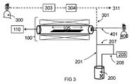
図3は、次の試験のために使用された析出装置の概略図である。装置は、基体クーポン105を含有する中空管反応器100を含む。ポンプ110によって、含有物を中空管反応器100から取り出す。
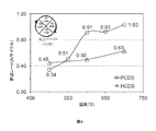
ヘキサクロロジシラン(HCDSまたはSi2Cl6)の比較熱分解試験を、4つの異なる温度(400、500、600および700℃)において、30分間、SiO2基体上で、図3の析出装置において実行した。熱壁管反応器を1トルに保持し、キャリア気体として50sccmのN2を使用して、反応チャンバー中へHCDSの4sccmの連続流を用いた。
Si基体上で、500〜700℃の温度範囲において酸化剤としてO3を用いて、PCDSを使用してSiO2 ALDを実行した。図3の反応燃焼室を1トルで制御し、そして50sccmのN2を連続的に流した。ALDプロセスは、次のステップを含んだ:1)10秒間、反応チャンバー中に4sccmのPCDSのパルスを供給し、2)90秒間、50sccmのN2によって過剰量の前駆体をパージし、3)10秒、約7.2%のO3/O2(O2:100sccm)を供給し、4)30秒間、50sccmのN2によって過剰量のO3/O2をパージする。析出された層が、フィルム特徴に関して適切な厚さ(すなわち、100Å以上)を達成するまで、順序1)〜4)を200サイクル繰り返した。この方法は、PCDSと同一のALDプロセス条件で、PCDSをHCDSで置き換えて繰り返した。PCDSを使用する4つの別個のクーポン基体位置(円形)およびHCDSを使用する4つの別個のクーポン基体位置(三角形)からの平均析出レートを図6に示す。
実施例2の結果に基づき、SiO2 ALD成長挙動のPCDSパルス時間依存性は、2つの温度、550℃および600℃において試験され、そして結果を図7に示す。PCDSのパルス時間が550℃(ひし形)および600℃(正方形)の両方において変動したことを除き、実施例2における温度依存性試験のために使用されたものと同一プロセス条件をこの評価に適応した。両温度において、安定な平均析出レートが、600℃においてクーポン:0.91〜0.94Å/サイクルおよび550℃において0.50〜0.52Å/サイクルで、3〜5の位置から、10〜15秒のPCDSのパルス時間で観察される。安定な析出レートは、ALD飽和の特徴であると考えられる。
550、600、650および700℃においてSi基体上でPCDSから実施例2において析出されたSiO2 ALDフィルムに関して、フィルム組成物を試験するために、XPS分析が実行された。図8a〜dは、5元素、Si、Cl、C、NおよびOのXPS深さ分布の結果を示す。Cl、CおよびNは、フィルムで検出されなかった。XPSスパッタエネルギーは、550℃および600℃において析出されたものよりも、650℃および700℃において析出されたフィルムに関して、より高く設定された。結果として、650℃および700℃において析出されたフィルムのエッチ時間に関する分析結果は、550℃および600℃において析出されたフィルムの同等のエッチ時間よりも、より深く侵入する。
ALDによって析出されたSiO2フィルムの段差被覆は、600℃において、8マイクロメートルの深さを有するアスペクト比(AR)=40を有するホールを有するパターンウエハ上で試験された。図3の反応燃焼室を1トルで制御し、そして50sccmのN2を連続的に流した。ALDプロセスは、次のステップを含んだ:1)10秒間、反応チャンバー中に4sccmのPCDSのパルスを供給し、2)90秒間、50sccmのN2によって過剰量の前駆体をパージし、3)10秒、約7.2%のO3/O2(O2:100sccm)を供給し、4)10秒間、50sccmのN2によって過剰量のO3/O2をパージする。順序1)〜4)を350サイクル繰り返した。図9および9a〜cは、全ホール(図9)および図9内の3つの異なる位置:(図9a)上部段差被覆=93%、(図9b)中央(上部から約2マイクロメートルの深さ)段差被覆=77%および(図9c)低部段差被覆=73%における得られた段差被覆を示す走査電子顕微鏡写真である。
SiO2フィルムは、PCDS、酸化剤としてH2Oおよび触媒としてトリエチルアミン(TEA)を用いるALDを使用して析出された。図3の反応燃焼室を5トル、50〜100℃の温度で制御し、そして200sccmのArを連続的に流した。析出プロセスは、次のステップを含んだ:1)10秒間、反応燃焼室中に1sccmのPCDSおよび50sccmのTEAのパルスを導入し、2)10秒間、1slmのArによって過剰量のPCDSおよびTEAをパージし、3)20秒、燃焼室に15sccmのH2Oおよび50sccmのTEAおよび1slmのArを導入し、4)20秒間、1slmのArによって過剰量のH2OおよびTEAをパージする。順序1)〜4)を300サイクル繰り返した。
SiNフィルムは、Si供給源としてPCDS(円形)またはHCDS(正方形)、および窒化物形成供給源としてアンモニア(NH3)を使用して、CVDによって析出された。図3の反応燃焼室を1トルで制御し、温度を450℃〜600℃で変動させ、そして100sccmのArを連続的に流した。析出された層が適切な厚さに達するまで、1sccmのSi供給源および25sccmのNH3の混合気体流を60〜120分間、反応燃焼室に供給した。図12は、HCDS+NH3よりも、PCDS+NH3によって得られた析出レート(白抜き)および屈折率(黒塗り)を例示するグラフである。
SiNフィルムは、Si供給源としてPCDS(円形)、HCDS(正方形)またはOCTS(オクタクロロトリシラン)(三角形)、および窒化物形成供給源としてアンモニア(NH3)を使用して、ALDによって析出された。図3の反応燃焼室を5トルで制御し、温度を350℃〜600℃で変動させ、そして100sccmのArを連続的に流した。析出プロセスは、次のステップを含む:1)10秒間、反応燃焼室中に1sccmのSi供給源のパルスを導入し、2)10秒間、1slmのArによって反応燃焼室から過剰量のSi供給源をパージし、3)反応燃焼室に50sccmのNH3を導入し、4)20秒間、1slmのArによって過剰量のNH3をパージする。析出された層が、100Å以上の適切な厚さを達成するまで、順序1)〜4)を200〜400サイクル繰り返した。
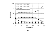
SiCフィルムは、Si供給源としてPCDSまたはHCDS、および炭素供給源としてトリメチルアルミニウム(TMA)を使用して、ALDによって析出された。図3の反応燃焼室を8トルで制御し、温度を350℃〜400℃で変動させ、そして10sccmのN2を連続的に流した。析出プロセスは、次のステップを含む:1)15秒間、反応燃焼室中に0.8sccmのSi供給源のパルスを導入し、2)30秒間、25sccmのN2によって反応燃焼室から過剰量のSi供給源をパージし、3)反応燃焼室に1.8sccmのTMAを導入し、4)60秒間、25sccmのN2によって反応燃焼室から過剰量のTMAをパージする。析出された層が、100Å以上の適切な厚さを達成するまで、順序1)〜4)を290サイクル繰り返した。図15は、400℃においてPCDSを使用して析出されたSiCフィルムのXPS深さ分布が、O、Al、Cl不純物を含むことを示す。図16は、測定位置に基づく、フィルムの厚さ(白抜き)および屈折率(黒塗り)を示す。このグラフは、HCDS(三角形)+TMAによる場合よりも、PCDS(正方形)+TMAで、より高い屈折率が得られたことを例示する。より高い屈折率を有するフィルム(すなわち、PCDS+TMAから)は、より低い屈折率を有するもの(すなわち、HCDS+TMAから)よりも高密度であり得、ウェットエッチ抵抗を増強し得る。
図17は、実施例10の試験のために使用された析出装置の概略図である。この装置は、ウエハ段階101を含有する反応器100を含む。ウエハは、ポンプ108に接続しているロードロックチャンバー102によってウエハ段階101に移される。シャワーヘッド103は、反応器100の上部に位置し、プラズマは、RF発生器106によって発生し得る。乾燥ポンプ105によって、反応器100の含有物が除去される。
Claims (15)
- 基体上に酸化ケイ素フィルムを析出する熱ALD法であって、
a)前記基体を含有する反応器を、約500℃〜約800℃の範囲の温度および約0.1〜約10トル(13Pa〜1,333Pa)の範囲の圧力に設定することと;
b)前記反応チャンバー中にペンタクロロジシランの蒸気を導入して、前記基体上でケイ素含有層を形成することと;
c)酸素含有反応物と、前記ケイ素含有層とを反応させて、約0.4Å(0.04nm)〜約1.5Å(0.15nm)の範囲のサイクルあたりの成長を有する酸化ケイ素フィルムの層を形成することと;
d)ステップb)およびc)を繰り返すことと
を含んでなる、方法。 - 前記酸素含有反応物が、オゾンおよび酸素の混合物である、請求項1に記載の方法。
- 前記混合物が、少なくとも5%v/vのオゾンを含んでなる、請求項2に記載の方法。
- 前記基体が、約10:1〜約100:1のアスペクト比を有するホールまたはトレンチを含んでなり、前記ホールまたはトレンチ上で約80%〜約100%の段差被覆の前記酸化ケイ素フィルムを得ることをさらに含んでなる、請求項1〜3のいずれか一項に記載の方法。
- 前記酸化ケイ素フィルムが、プラズマを使用せずに析出される、請求項1〜4のいずれか一項に記載の方法。
- 前記サイクルあたりの成長が、約0.75Å(0.075nm)〜約1Å(0.1nm)の範囲である、請求項1〜5のいずれか一項に記載の方法。
- 基体上に窒化ケイ素フィルムを析出する熱ALD法であって、
a)前記基体を含有する反応器を、約450℃〜約650℃の範囲の温度および約0.1〜約100トル(13Pa〜13,332Pa)の範囲の圧力に設定することと;
b)前記反応チャンバー中にペンタクロロジシランの蒸気を導入して、前記基体上でケイ素含有層を形成することと;
c)窒素含有反応物と、前記ケイ素含有層とを反応させて、約0.3Å(0.03nm)〜約2Å(0.2nm)の範囲のサイクルあたりの成長および約1.8〜2.1の範囲の屈折率を有する窒化ケイ素フィルムの層を形成することと;
d)ステップb)およびc)を繰り返すことと
を含んでなる、方法。 - 前記窒素含有反応物がNH3である、請求項7に記載の方法。
- 前記窒化ケイ素フィルムが、プラズマを使用せずに析出される、請求項7または8に記載の方法。
- 基体上に非晶質または多結晶質ケイ素フィルムを析出する熱蒸着法であって、
a)前記基体を含有する反応器を、約550℃〜約800℃の範囲の温度および約0.1〜約100トル(13Pa〜13,332Pa)の範囲の圧力に設定することと;
b)前記反応チャンバー中にペンタクロロジシランの蒸気を導入して、前記基体上で前記ケイ素フィルムを形成することと
を含んでなる、方法。 - 還元気体を導入することをさらに含んでなる、請求項10に記載の方法。
- 前記ケイ素フィルムが約0原子%〜5原子%のC;約0原子%〜1原子%のN;および約0原子%〜1原子%のClを含有する、請求項10または11に記載の方法。
- 前記ケイ素フィルムが非晶質ケイ素フィルムである、請求項10〜12のいずれか一項に記載の方法。
- 前記ケイ素フィルムが多ケイ素フィルムである、請求項10〜12のいずれか一項に記載の方法。
- 前記基体が、約10:1〜約100:1のアスペクト比を有するホールまたはトレンチを含んでなり、前記ホールまたはトレンチ上で約80%〜約100%の段差被覆の前記ケイ素フィルムを得ることをさらに含んでなる、請求項10〜14のいずれか一項に記載の方法。
Applications Claiming Priority (3)
| Application Number | Priority Date | Filing Date | Title |
|---|---|---|---|
| US14/979,816 | 2015-12-28 | ||
| US14/979,816 US9633838B2 (en) | 2015-12-28 | 2015-12-28 | Vapor deposition of silicon-containing films using penta-substituted disilanes |
| PCT/IB2016/001962 WO2017115147A2 (en) | 2015-12-28 | 2016-12-16 | Vapor disposition of silicon-containing films using penta-substituted disilanes |
Publications (2)
| Publication Number | Publication Date |
|---|---|
| JP2019501528A true JP2019501528A (ja) | 2019-01-17 |
| JP2019501528A5 JP2019501528A5 (ja) | 2020-01-23 |
Family
ID=55749599
Family Applications (1)
| Application Number | Title | Priority Date | Filing Date |
|---|---|---|---|
| JP2018530071A Pending JP2019501528A (ja) | 2015-12-28 | 2016-12-16 | 五置換ジシランを使用するケイ素含有フィルムの蒸着 |
Country Status (7)
| Country | Link |
|---|---|
| US (3) | US9633838B2 (ja) |
| EP (1) | EP3400607A4 (ja) |
| JP (1) | JP2019501528A (ja) |
| KR (1) | KR20180099716A (ja) |
| CN (1) | CN108475636B (ja) |
| SG (1) | SG11201805070TA (ja) |
| WO (1) | WO2017115147A2 (ja) |
Families Citing this family (347)
| Publication number | Priority date | Publication date | Assignee | Title |
|---|---|---|---|---|
| US10378106B2 (en) | 2008-11-14 | 2019-08-13 | Asm Ip Holding B.V. | Method of forming insulation film by modified PEALD |
| US9394608B2 (en) | 2009-04-06 | 2016-07-19 | Asm America, Inc. | Semiconductor processing reactor and components thereof |
| US8802201B2 (en) | 2009-08-14 | 2014-08-12 | Asm America, Inc. | Systems and methods for thin-film deposition of metal oxides using excited nitrogen-oxygen species |
| US9312155B2 (en) | 2011-06-06 | 2016-04-12 | Asm Japan K.K. | High-throughput semiconductor-processing apparatus equipped with multiple dual-chamber modules |
| US10364496B2 (en) | 2011-06-27 | 2019-07-30 | Asm Ip Holding B.V. | Dual section module having shared and unshared mass flow controllers |
| US10854498B2 (en) | 2011-07-15 | 2020-12-01 | Asm Ip Holding B.V. | Wafer-supporting device and method for producing same |
| US20130023129A1 (en) | 2011-07-20 | 2013-01-24 | Asm America, Inc. | Pressure transmitter for a semiconductor processing environment |
| US9017481B1 (en) | 2011-10-28 | 2015-04-28 | Asm America, Inc. | Process feed management for semiconductor substrate processing |
| US9659799B2 (en) | 2012-08-28 | 2017-05-23 | Asm Ip Holding B.V. | Systems and methods for dynamic semiconductor process scheduling |
| US10714315B2 (en) | 2012-10-12 | 2020-07-14 | Asm Ip Holdings B.V. | Semiconductor reaction chamber showerhead |
| US20160376700A1 (en) | 2013-02-01 | 2016-12-29 | Asm Ip Holding B.V. | System for treatment of deposition reactor |
| US9484191B2 (en) | 2013-03-08 | 2016-11-01 | Asm Ip Holding B.V. | Pulsed remote plasma method and system |
| US9589770B2 (en) | 2013-03-08 | 2017-03-07 | Asm Ip Holding B.V. | Method and systems for in-situ formation of intermediate reactive species |
| US9240412B2 (en) | 2013-09-27 | 2016-01-19 | Asm Ip Holding B.V. | Semiconductor structure and device and methods of forming same using selective epitaxial process |
| US10804094B2 (en) | 2016-05-06 | 2020-10-13 | Applied Materials, Inc. | Methods of depositing SiCON with C, O and N compositional control |
| US11549181B2 (en) | 2013-11-22 | 2023-01-10 | Applied Materials, Inc. | Methods for atomic layer deposition of SiCO(N) using halogenated silylamides |
| JP6495025B2 (ja) | 2014-01-31 | 2019-04-03 | ラム リサーチ コーポレーションLam Research Corporation | 真空統合ハードマスク処理および装置 |
| US10683571B2 (en) | 2014-02-25 | 2020-06-16 | Asm Ip Holding B.V. | Gas supply manifold and method of supplying gases to chamber using same |
| US10167557B2 (en) | 2014-03-18 | 2019-01-01 | Asm Ip Holding B.V. | Gas distribution system, reactor including the system, and methods of using the same |
| US11015245B2 (en) | 2014-03-19 | 2021-05-25 | Asm Ip Holding B.V. | Gas-phase reactor and system having exhaust plenum and components thereof |
| US10858737B2 (en) | 2014-07-28 | 2020-12-08 | Asm Ip Holding B.V. | Showerhead assembly and components thereof |
| US9890456B2 (en) | 2014-08-21 | 2018-02-13 | Asm Ip Holding B.V. | Method and system for in situ formation of gas-phase compounds |
| US10941490B2 (en) | 2014-10-07 | 2021-03-09 | Asm Ip Holding B.V. | Multiple temperature range susceptor, assembly, reactor and system including the susceptor, and methods of using the same |
| US9657845B2 (en) | 2014-10-07 | 2017-05-23 | Asm Ip Holding B.V. | Variable conductance gas distribution apparatus and method |
| KR102263121B1 (ko) | 2014-12-22 | 2021-06-09 | 에이에스엠 아이피 홀딩 비.브이. | 반도체 소자 및 그 제조 방법 |
| US10529542B2 (en) | 2015-03-11 | 2020-01-07 | Asm Ip Holdings B.V. | Cross-flow reactor and method |
| US10276355B2 (en) | 2015-03-12 | 2019-04-30 | Asm Ip Holding B.V. | Multi-zone reactor, system including the reactor, and method of using the same |
| US10458018B2 (en) | 2015-06-26 | 2019-10-29 | Asm Ip Holding B.V. | Structures including metal carbide material, devices including the structures, and methods of forming same |
| US10600673B2 (en) | 2015-07-07 | 2020-03-24 | Asm Ip Holding B.V. | Magnetic susceptor to baseplate seal |
| US10083836B2 (en) | 2015-07-24 | 2018-09-25 | Asm Ip Holding B.V. | Formation of boron-doped titanium metal films with high work function |
| US9960072B2 (en) | 2015-09-29 | 2018-05-01 | Asm Ip Holding B.V. | Variable adjustment for precise matching of multiple chamber cavity housings |
| US10211308B2 (en) | 2015-10-21 | 2019-02-19 | Asm Ip Holding B.V. | NbMC layers |
| US10322384B2 (en) | 2015-11-09 | 2019-06-18 | Asm Ip Holding B.V. | Counter flow mixer for process chamber |
| US11139308B2 (en) | 2015-12-29 | 2021-10-05 | Asm Ip Holding B.V. | Atomic layer deposition of III-V compounds to form V-NAND devices |
| US10468251B2 (en) | 2016-02-19 | 2019-11-05 | Asm Ip Holding B.V. | Method for forming spacers using silicon nitride film for spacer-defined multiple patterning |
| US10529554B2 (en) | 2016-02-19 | 2020-01-07 | Asm Ip Holding B.V. | Method for forming silicon nitride film selectively on sidewalls or flat surfaces of trenches |
| US10501866B2 (en) | 2016-03-09 | 2019-12-10 | Asm Ip Holding B.V. | Gas distribution apparatus for improved film uniformity in an epitaxial system |
| US10343920B2 (en) | 2016-03-18 | 2019-07-09 | Asm Ip Holding B.V. | Aligned carbon nanotubes |
| US9892913B2 (en) | 2016-03-24 | 2018-02-13 | Asm Ip Holding B.V. | Radial and thickness control via biased multi-port injection settings |
| US10865475B2 (en) | 2016-04-21 | 2020-12-15 | Asm Ip Holding B.V. | Deposition of metal borides and silicides |
| US10190213B2 (en) | 2016-04-21 | 2019-01-29 | Asm Ip Holding B.V. | Deposition of metal borides |
| US10032628B2 (en) | 2016-05-02 | 2018-07-24 | Asm Ip Holding B.V. | Source/drain performance through conformal solid state doping |
| US10367080B2 (en) | 2016-05-02 | 2019-07-30 | Asm Ip Holding B.V. | Method of forming a germanium oxynitride film |
| US10480070B2 (en) | 2016-05-12 | 2019-11-19 | Versum Materials Us, Llc | Delivery container with flow distributor |
| KR102592471B1 (ko) | 2016-05-17 | 2023-10-20 | 에이에스엠 아이피 홀딩 비.브이. | 금속 배선 형성 방법 및 이를 이용한 반도체 장치의 제조 방법 |
| US11453943B2 (en) | 2016-05-25 | 2022-09-27 | Asm Ip Holding B.V. | Method for forming carbon-containing silicon/metal oxide or nitride film by ALD using silicon precursor and hydrocarbon precursor |
| US10388509B2 (en) | 2016-06-28 | 2019-08-20 | Asm Ip Holding B.V. | Formation of epitaxial layers via dislocation filtering |
| US9859151B1 (en) | 2016-07-08 | 2018-01-02 | Asm Ip Holding B.V. | Selective film deposition method to form air gaps |
| US10612137B2 (en) | 2016-07-08 | 2020-04-07 | Asm Ip Holdings B.V. | Organic reactants for atomic layer deposition |
| US10714385B2 (en) | 2016-07-19 | 2020-07-14 | Asm Ip Holding B.V. | Selective deposition of tungsten |
| US20180033614A1 (en) * | 2016-07-27 | 2018-02-01 | Versum Materials Us, Llc | Compositions and Methods Using Same for Carbon Doped Silicon Containing Films |
| KR102354490B1 (ko) | 2016-07-27 | 2022-01-21 | 에이에스엠 아이피 홀딩 비.브이. | 기판 처리 방법 |
| US10395919B2 (en) | 2016-07-28 | 2019-08-27 | Asm Ip Holding B.V. | Method and apparatus for filling a gap |
| KR102532607B1 (ko) | 2016-07-28 | 2023-05-15 | 에이에스엠 아이피 홀딩 비.브이. | 기판 가공 장치 및 그 동작 방법 |
| US9887082B1 (en) | 2016-07-28 | 2018-02-06 | Asm Ip Holding B.V. | Method and apparatus for filling a gap |
| US9812320B1 (en) | 2016-07-28 | 2017-11-07 | Asm Ip Holding B.V. | Method and apparatus for filling a gap |
| US9865455B1 (en) * | 2016-09-07 | 2018-01-09 | Lam Research Corporation | Nitride film formed by plasma-enhanced and thermal atomic layer deposition process |
| CN109790036B (zh) * | 2016-09-28 | 2022-11-04 | 美国陶氏有机硅公司 | 氯二硅氮烷 |
| US10410943B2 (en) | 2016-10-13 | 2019-09-10 | Asm Ip Holding B.V. | Method for passivating a surface of a semiconductor and related systems |
| US10643826B2 (en) | 2016-10-26 | 2020-05-05 | Asm Ip Holdings B.V. | Methods for thermally calibrating reaction chambers |
| US11532757B2 (en) | 2016-10-27 | 2022-12-20 | Asm Ip Holding B.V. | Deposition of charge trapping layers |
| US10643904B2 (en) | 2016-11-01 | 2020-05-05 | Asm Ip Holdings B.V. | Methods for forming a semiconductor device and related semiconductor device structures |
| US10714350B2 (en) | 2016-11-01 | 2020-07-14 | ASM IP Holdings, B.V. | Methods for forming a transition metal niobium nitride film on a substrate by atomic layer deposition and related semiconductor device structures |
| US10229833B2 (en) | 2016-11-01 | 2019-03-12 | Asm Ip Holding B.V. | Methods for forming a transition metal nitride film on a substrate by atomic layer deposition and related semiconductor device structures |
| US10435790B2 (en) | 2016-11-01 | 2019-10-08 | Asm Ip Holding B.V. | Method of subatmospheric plasma-enhanced ALD using capacitively coupled electrodes with narrow gap |
| US10134757B2 (en) | 2016-11-07 | 2018-11-20 | Asm Ip Holding B.V. | Method of processing a substrate and a device manufactured by using the method |
| KR102546317B1 (ko) | 2016-11-15 | 2023-06-21 | 에이에스엠 아이피 홀딩 비.브이. | 기체 공급 유닛 및 이를 포함하는 기판 처리 장치 |
| US10340135B2 (en) | 2016-11-28 | 2019-07-02 | Asm Ip Holding B.V. | Method of topologically restricted plasma-enhanced cyclic deposition of silicon or metal nitride |
| KR20180068582A (ko) | 2016-12-14 | 2018-06-22 | 에이에스엠 아이피 홀딩 비.브이. | 기판 처리 장치 |
| US11581186B2 (en) | 2016-12-15 | 2023-02-14 | Asm Ip Holding B.V. | Sequential infiltration synthesis apparatus |
| US11447861B2 (en) | 2016-12-15 | 2022-09-20 | Asm Ip Holding B.V. | Sequential infiltration synthesis apparatus and a method of forming a patterned structure |
| KR20180070971A (ko) | 2016-12-19 | 2018-06-27 | 에이에스엠 아이피 홀딩 비.브이. | 기판 처리 장치 |
| US10269558B2 (en) * | 2016-12-22 | 2019-04-23 | Asm Ip Holding B.V. | Method of forming a structure on a substrate |
| US10867788B2 (en) | 2016-12-28 | 2020-12-15 | Asm Ip Holding B.V. | Method of forming a structure on a substrate |
| US10049882B1 (en) * | 2017-01-25 | 2018-08-14 | Samsung Electronics Co., Ltd. | Method for fabricating semiconductor device including forming a dielectric layer on a structure having a height difference using ALD |
| US10655221B2 (en) | 2017-02-09 | 2020-05-19 | Asm Ip Holding B.V. | Method for depositing oxide film by thermal ALD and PEALD |
| US10468261B2 (en) | 2017-02-15 | 2019-11-05 | Asm Ip Holding B.V. | Methods for forming a metallic film on a substrate by cyclical deposition and related semiconductor device structures |
| US10224224B2 (en) | 2017-03-10 | 2019-03-05 | Micromaterials, LLC | High pressure wafer processing systems and related methods |
| US10283353B2 (en) | 2017-03-29 | 2019-05-07 | Asm Ip Holding B.V. | Method of reforming insulating film deposited on substrate with recess pattern |
| US10529563B2 (en) | 2017-03-29 | 2020-01-07 | Asm Ip Holdings B.V. | Method for forming doped metal oxide films on a substrate by cyclical deposition and related semiconductor device structures |
| KR102271768B1 (ko) * | 2017-04-07 | 2021-06-30 | 어플라이드 머티어리얼스, 인코포레이티드 | 반응성 어닐링을 사용하는 갭충전 |
| KR102457289B1 (ko) | 2017-04-25 | 2022-10-21 | 에이에스엠 아이피 홀딩 비.브이. | 박막 증착 방법 및 반도체 장치의 제조 방법 |
| US10892156B2 (en) | 2017-05-08 | 2021-01-12 | Asm Ip Holding B.V. | Methods for forming a silicon nitride film on a substrate and related semiconductor device structures |
| US10446393B2 (en) | 2017-05-08 | 2019-10-15 | Asm Ip Holding B.V. | Methods for forming silicon-containing epitaxial layers and related semiconductor device structures |
| US10770286B2 (en) | 2017-05-08 | 2020-09-08 | Asm Ip Holdings B.V. | Methods for selectively forming a silicon nitride film on a substrate and related semiconductor device structures |
| US10796912B2 (en) | 2017-05-16 | 2020-10-06 | Lam Research Corporation | Eliminating yield impact of stochastics in lithography |
| US10622214B2 (en) | 2017-05-25 | 2020-04-14 | Applied Materials, Inc. | Tungsten defluorination by high pressure treatment |
| US10847360B2 (en) * | 2017-05-25 | 2020-11-24 | Applied Materials, Inc. | High pressure treatment of silicon nitride film |
| US10242885B2 (en) * | 2017-05-26 | 2019-03-26 | Applied Materials, Inc. | Selective dry etching of metal films comprising multiple metal oxides |
| US10504742B2 (en) | 2017-05-31 | 2019-12-10 | Asm Ip Holding B.V. | Method of atomic layer etching using hydrogen plasma |
| US10886123B2 (en) | 2017-06-02 | 2021-01-05 | Asm Ip Holding B.V. | Methods for forming low temperature semiconductor layers and related semiconductor device structures |
| JP7190450B2 (ja) | 2017-06-02 | 2022-12-15 | アプライド マテリアルズ インコーポレイテッド | 炭化ホウ素ハードマスクのドライストリッピング |
| US11306395B2 (en) | 2017-06-28 | 2022-04-19 | Asm Ip Holding B.V. | Methods for depositing a transition metal nitride film on a substrate by atomic layer deposition and related deposition apparatus |
| US10685834B2 (en) | 2017-07-05 | 2020-06-16 | Asm Ip Holdings B.V. | Methods for forming a silicon germanium tin layer and related semiconductor device structures |
| KR20190009245A (ko) | 2017-07-18 | 2019-01-28 | 에이에스엠 아이피 홀딩 비.브이. | 반도체 소자 구조물 형성 방법 및 관련된 반도체 소자 구조물 |
| US11018002B2 (en) | 2017-07-19 | 2021-05-25 | Asm Ip Holding B.V. | Method for selectively depositing a Group IV semiconductor and related semiconductor device structures |
| US11374112B2 (en) | 2017-07-19 | 2022-06-28 | Asm Ip Holding B.V. | Method for depositing a group IV semiconductor and related semiconductor device structures |
| US10541333B2 (en) | 2017-07-19 | 2020-01-21 | Asm Ip Holding B.V. | Method for depositing a group IV semiconductor and related semiconductor device structures |
| US10605530B2 (en) | 2017-07-26 | 2020-03-31 | Asm Ip Holding B.V. | Assembly of a liner and a flange for a vertical furnace as well as the liner and the vertical furnace |
| US10312055B2 (en) | 2017-07-26 | 2019-06-04 | Asm Ip Holding B.V. | Method of depositing film by PEALD using negative bias |
| US10590535B2 (en) | 2017-07-26 | 2020-03-17 | Asm Ip Holdings B.V. | Chemical treatment, deposition and/or infiltration apparatus and method for using the same |
| TWI791547B (zh) * | 2017-07-31 | 2023-02-11 | 中國大陸商南大光電半導體材料有限公司 | 製備五氯二矽烷之方法及包含五氯二矽烷之經純化的反應產物 |
| TWI784022B (zh) | 2017-07-31 | 2022-11-21 | 中國大陸商南大光電半導體材料有限公司 | 1,1,1-參(二甲胺基)二矽烷及其製備方法 |
| JP6840051B2 (ja) * | 2017-08-02 | 2021-03-10 | 東京エレクトロン株式会社 | タングステン膜上へシリコン酸化膜を形成する方法および装置 |
| US10692741B2 (en) | 2017-08-08 | 2020-06-23 | Asm Ip Holdings B.V. | Radiation shield |
| US10770336B2 (en) | 2017-08-08 | 2020-09-08 | Asm Ip Holding B.V. | Substrate lift mechanism and reactor including same |
| US10249524B2 (en) | 2017-08-09 | 2019-04-02 | Asm Ip Holding B.V. | Cassette holder assembly for a substrate cassette and holding member for use in such assembly |
| US11139191B2 (en) | 2017-08-09 | 2021-10-05 | Asm Ip Holding B.V. | Storage apparatus for storing cassettes for substrates and processing apparatus equipped therewith |
| US11769682B2 (en) | 2017-08-09 | 2023-09-26 | Asm Ip Holding B.V. | Storage apparatus for storing cassettes for substrates and processing apparatus equipped therewith |
| CN111095513B (zh) | 2017-08-18 | 2023-10-31 | 应用材料公司 | 高压高温退火腔室 |
| US10276411B2 (en) | 2017-08-18 | 2019-04-30 | Applied Materials, Inc. | High pressure and high temperature anneal chamber |
| USD900036S1 (en) | 2017-08-24 | 2020-10-27 | Asm Ip Holding B.V. | Heater electrical connector and adapter |
| US11830730B2 (en) | 2017-08-29 | 2023-11-28 | Asm Ip Holding B.V. | Layer forming method and apparatus |
| US11056344B2 (en) | 2017-08-30 | 2021-07-06 | Asm Ip Holding B.V. | Layer forming method |
| KR102491945B1 (ko) | 2017-08-30 | 2023-01-26 | 에이에스엠 아이피 홀딩 비.브이. | 기판 처리 장치 |
| US11295980B2 (en) | 2017-08-30 | 2022-04-05 | Asm Ip Holding B.V. | Methods for depositing a molybdenum metal film over a dielectric surface of a substrate by a cyclical deposition process and related semiconductor device structures |
| SG11202001450UA (en) | 2017-09-12 | 2020-03-30 | Applied Materials Inc | Apparatus and methods for manufacturing semiconductor structures using protective barrier layer |
| US10607895B2 (en) | 2017-09-18 | 2020-03-31 | Asm Ip Holdings B.V. | Method for forming a semiconductor device structure comprising a gate fill metal |
| KR102630301B1 (ko) | 2017-09-21 | 2024-01-29 | 에이에스엠 아이피 홀딩 비.브이. | 침투성 재료의 순차 침투 합성 방법 처리 및 이를 이용하여 형성된 구조물 및 장치 |
| US10844484B2 (en) | 2017-09-22 | 2020-11-24 | Asm Ip Holding B.V. | Apparatus for dispensing a vapor phase reactant to a reaction chamber and related methods |
| US10658205B2 (en) * | 2017-09-28 | 2020-05-19 | Asm Ip Holdings B.V. | Chemical dispensing apparatus and methods for dispensing a chemical to a reaction chamber |
| DE102018110837A1 (de) | 2017-09-29 | 2019-04-04 | Taiwan Semiconductor Manufacturing Co., Ltd. | Prozesse zur Bildung von Merkmalen mit einem niedrigen K-Wert und dadurch gebildete Aufbauten |
| US10304677B2 (en) | 2017-09-29 | 2019-05-28 | Taiwan Semiconductor Manufacturing Co., Ltd. | Low-k feature formation processes and structures formed thereby |
| US10403504B2 (en) | 2017-10-05 | 2019-09-03 | Asm Ip Holding B.V. | Method for selectively depositing a metallic film on a substrate |
| US10319588B2 (en) | 2017-10-10 | 2019-06-11 | Asm Ip Holding B.V. | Method for depositing a metal chalcogenide on a substrate by cyclical deposition |
| US10923344B2 (en) | 2017-10-30 | 2021-02-16 | Asm Ip Holding B.V. | Methods for forming a semiconductor structure and related semiconductor structures |
| US10643867B2 (en) | 2017-11-03 | 2020-05-05 | Applied Materials, Inc. | Annealing system and method |
| EP4321649A3 (en) | 2017-11-11 | 2024-05-15 | Micromaterials LLC | Gas delivery system for high pressure processing chamber |
| KR102443047B1 (ko) | 2017-11-16 | 2022-09-14 | 에이에스엠 아이피 홀딩 비.브이. | 기판 처리 장치 방법 및 그에 의해 제조된 장치 |
| US10910262B2 (en) | 2017-11-16 | 2021-02-02 | Asm Ip Holding B.V. | Method of selectively depositing a capping layer structure on a semiconductor device structure |
| CN111373519B (zh) | 2017-11-16 | 2021-11-23 | 应用材料公司 | 高压蒸气退火处理设备 |
| CN111432920A (zh) | 2017-11-17 | 2020-07-17 | 应用材料公司 | 用于高压处理系统的冷凝器系统 |
| US11022879B2 (en) | 2017-11-24 | 2021-06-01 | Asm Ip Holding B.V. | Method of forming an enhanced unexposed photoresist layer |
| KR102597978B1 (ko) | 2017-11-27 | 2023-11-06 | 에이에스엠 아이피 홀딩 비.브이. | 배치 퍼니스와 함께 사용하기 위한 웨이퍼 카세트를 보관하기 위한 보관 장치 |
| US11639811B2 (en) | 2017-11-27 | 2023-05-02 | Asm Ip Holding B.V. | Apparatus including a clean mini environment |
| US10510852B2 (en) * | 2017-11-28 | 2019-12-17 | Taiwan Semiconductor Manufacturing Company, Ltd. | Low-k feature formation processes and structures formed thereby |
| US10290508B1 (en) | 2017-12-05 | 2019-05-14 | Asm Ip Holding B.V. | Method for forming vertical spacers for spacer-defined patterning |
| EP3514128A1 (en) * | 2018-01-18 | 2019-07-24 | Heraeus GMSI LLC | Process for manufacturing a silicon carbide coated body |
| EP3514129A1 (en) * | 2018-01-18 | 2019-07-24 | Heraeus GMSI LLC | Process for manufacturing a silicon carbide coated body |
| US10872771B2 (en) | 2018-01-16 | 2020-12-22 | Asm Ip Holding B. V. | Method for depositing a material film on a substrate within a reaction chamber by a cyclical deposition process and related device structures |
| TW202325889A (zh) | 2018-01-19 | 2023-07-01 | 荷蘭商Asm 智慧財產控股公司 | 沈積方法 |
| US11482412B2 (en) | 2018-01-19 | 2022-10-25 | Asm Ip Holding B.V. | Method for depositing a gap-fill layer by plasma-assisted deposition |
| USD903477S1 (en) | 2018-01-24 | 2020-12-01 | Asm Ip Holdings B.V. | Metal clamp |
| WO2019147400A1 (en) | 2018-01-24 | 2019-08-01 | Applied Materials, Inc. | Seam healing using high pressure anneal |
| US11018047B2 (en) | 2018-01-25 | 2021-05-25 | Asm Ip Holding B.V. | Hybrid lift pin |
| USD880437S1 (en) | 2018-02-01 | 2020-04-07 | Asm Ip Holding B.V. | Gas supply plate for semiconductor manufacturing apparatus |
| US10535516B2 (en) | 2018-02-01 | 2020-01-14 | Asm Ip Holdings B.V. | Method for depositing a semiconductor structure on a surface of a substrate and related semiconductor structures |
| US11081345B2 (en) | 2018-02-06 | 2021-08-03 | Asm Ip Holding B.V. | Method of post-deposition treatment for silicon oxide film |
| WO2019158960A1 (en) | 2018-02-14 | 2019-08-22 | Asm Ip Holding B.V. | A method for depositing a ruthenium-containing film on a substrate by a cyclical deposition process |
| US10896820B2 (en) | 2018-02-14 | 2021-01-19 | Asm Ip Holding B.V. | Method for depositing a ruthenium-containing film on a substrate by a cyclical deposition process |
| US10731249B2 (en) | 2018-02-15 | 2020-08-04 | Asm Ip Holding B.V. | Method of forming a transition metal containing film on a substrate by a cyclical deposition process, a method for supplying a transition metal halide compound to a reaction chamber, and related vapor deposition apparatus |
| KR102636427B1 (ko) | 2018-02-20 | 2024-02-13 | 에이에스엠 아이피 홀딩 비.브이. | 기판 처리 방법 및 장치 |
| US10658181B2 (en) | 2018-02-20 | 2020-05-19 | Asm Ip Holding B.V. | Method of spacer-defined direct patterning in semiconductor fabrication |
| US10975470B2 (en) | 2018-02-23 | 2021-04-13 | Asm Ip Holding B.V. | Apparatus for detecting or monitoring for a chemical precursor in a high temperature environment |
| US11473195B2 (en) | 2018-03-01 | 2022-10-18 | Asm Ip Holding B.V. | Semiconductor processing apparatus and a method for processing a substrate |
| US11629406B2 (en) | 2018-03-09 | 2023-04-18 | Asm Ip Holding B.V. | Semiconductor processing apparatus comprising one or more pyrometers for measuring a temperature of a substrate during transfer of the substrate |
| WO2019173006A1 (en) | 2018-03-09 | 2019-09-12 | Applied Materials, Inc. | High pressure annealing process for metal containing materials |
| US11114283B2 (en) | 2018-03-16 | 2021-09-07 | Asm Ip Holding B.V. | Reactor, system including the reactor, and methods of manufacturing and using same |
| KR102646467B1 (ko) | 2018-03-27 | 2024-03-11 | 에이에스엠 아이피 홀딩 비.브이. | 기판 상에 전극을 형성하는 방법 및 전극을 포함하는 반도체 소자 구조 |
| US11230766B2 (en) | 2018-03-29 | 2022-01-25 | Asm Ip Holding B.V. | Substrate processing apparatus and method |
| US10510536B2 (en) | 2018-03-29 | 2019-12-17 | Asm Ip Holding B.V. | Method of depositing a co-doped polysilicon film on a surface of a substrate within a reaction chamber |
| US11088002B2 (en) | 2018-03-29 | 2021-08-10 | Asm Ip Holding B.V. | Substrate rack and a substrate processing system and method |
| KR102501472B1 (ko) | 2018-03-30 | 2023-02-20 | 에이에스엠 아이피 홀딩 비.브이. | 기판 처리 방법 |
| US10714331B2 (en) | 2018-04-04 | 2020-07-14 | Applied Materials, Inc. | Method to fabricate thermally stable low K-FinFET spacer |
| US10950429B2 (en) | 2018-05-08 | 2021-03-16 | Applied Materials, Inc. | Methods of forming amorphous carbon hard mask layers and hard mask layers formed therefrom |
| TWI811348B (zh) | 2018-05-08 | 2023-08-11 | 荷蘭商Asm 智慧財產控股公司 | 藉由循環沉積製程於基板上沉積氧化物膜之方法及相關裝置結構 |
| TWI816783B (zh) | 2018-05-11 | 2023-10-01 | 荷蘭商Asm 智慧財產控股公司 | 用於基板上形成摻雜金屬碳化物薄膜之方法及相關半導體元件結構 |
| US10566188B2 (en) | 2018-05-17 | 2020-02-18 | Applied Materials, Inc. | Method to improve film stability |
| KR102596988B1 (ko) | 2018-05-28 | 2023-10-31 | 에이에스엠 아이피 홀딩 비.브이. | 기판 처리 방법 및 그에 의해 제조된 장치 |
| US10704141B2 (en) | 2018-06-01 | 2020-07-07 | Applied Materials, Inc. | In-situ CVD and ALD coating of chamber to control metal contamination |
| US11718913B2 (en) | 2018-06-04 | 2023-08-08 | Asm Ip Holding B.V. | Gas distribution system and reactor system including same |
| US11270899B2 (en) | 2018-06-04 | 2022-03-08 | Asm Ip Holding B.V. | Wafer handling chamber with moisture reduction |
| US11286562B2 (en) | 2018-06-08 | 2022-03-29 | Asm Ip Holding B.V. | Gas-phase chemical reactor and method of using same |
| KR102568797B1 (ko) | 2018-06-21 | 2023-08-21 | 에이에스엠 아이피 홀딩 비.브이. | 기판 처리 시스템 |
| US10797133B2 (en) | 2018-06-21 | 2020-10-06 | Asm Ip Holding B.V. | Method for depositing a phosphorus doped silicon arsenide film and related semiconductor device structures |
| JP2021529254A (ja) | 2018-06-27 | 2021-10-28 | エーエスエム・アイピー・ホールディング・ベー・フェー | 金属含有材料ならびに金属含有材料を含む膜および構造体を形成するための周期的堆積方法 |
| CN112292477A (zh) | 2018-06-27 | 2021-01-29 | Asm Ip私人控股有限公司 | 用于形成含金属的材料的循环沉积方法及包含含金属的材料的膜和结构 |
| US10612136B2 (en) | 2018-06-29 | 2020-04-07 | ASM IP Holding, B.V. | Temperature-controlled flange and reactor system including same |
| KR20200002519A (ko) | 2018-06-29 | 2020-01-08 | 에이에스엠 아이피 홀딩 비.브이. | 박막 증착 방법 및 반도체 장치의 제조 방법 |
| US10388513B1 (en) | 2018-07-03 | 2019-08-20 | Asm Ip Holding B.V. | Method for depositing silicon-free carbon-containing film as gap-fill layer by pulse plasma-assisted deposition |
| US10755922B2 (en) * | 2018-07-03 | 2020-08-25 | Asm Ip Holding B.V. | Method for depositing silicon-free carbon-containing film as gap-fill layer by pulse plasma-assisted deposition |
| US10767789B2 (en) | 2018-07-16 | 2020-09-08 | Asm Ip Holding B.V. | Diaphragm valves, valve components, and methods for forming valve components |
| US10748783B2 (en) | 2018-07-25 | 2020-08-18 | Applied Materials, Inc. | Gas delivery module |
| US10483099B1 (en) | 2018-07-26 | 2019-11-19 | Asm Ip Holding B.V. | Method for forming thermally stable organosilicon polymer film |
| US11043373B2 (en) * | 2018-07-31 | 2021-06-22 | Taiwan Semiconductor Manufacturing Company, Ltd. | Interconnect system with improved low-k dielectrics |
| US10675581B2 (en) | 2018-08-06 | 2020-06-09 | Applied Materials, Inc. | Gas abatement apparatus |
| US11053591B2 (en) | 2018-08-06 | 2021-07-06 | Asm Ip Holding B.V. | Multi-port gas injection system and reactor system including same |
| US10883175B2 (en) | 2018-08-09 | 2021-01-05 | Asm Ip Holding B.V. | Vertical furnace for processing substrates and a liner for use therein |
| US10829852B2 (en) | 2018-08-16 | 2020-11-10 | Asm Ip Holding B.V. | Gas distribution device for a wafer processing apparatus |
| US11430674B2 (en) | 2018-08-22 | 2022-08-30 | Asm Ip Holding B.V. | Sensor array, apparatus for dispensing a vapor phase reactant to a reaction chamber and related methods |
| US11072858B2 (en) * | 2018-09-05 | 2021-07-27 | Nova Engineering Films, Inc. | Pulsing mixture of precursor and supercritical fluid to treat substrate surface |
| KR20200030162A (ko) | 2018-09-11 | 2020-03-20 | 에이에스엠 아이피 홀딩 비.브이. | 박막 증착 방법 |
| US11024523B2 (en) | 2018-09-11 | 2021-06-01 | Asm Ip Holding B.V. | Substrate processing apparatus and method |
| US11049751B2 (en) | 2018-09-14 | 2021-06-29 | Asm Ip Holding B.V. | Cassette supply system to store and handle cassettes and processing apparatus equipped therewith |
| CN110970344A (zh) | 2018-10-01 | 2020-04-07 | Asm Ip控股有限公司 | 衬底保持设备、包含所述设备的系统及其使用方法 |
| US11232963B2 (en) | 2018-10-03 | 2022-01-25 | Asm Ip Holding B.V. | Substrate processing apparatus and method |
| US20210380418A1 (en) * | 2018-10-05 | 2021-12-09 | Versum Materials Us, Llc | High temperature atomic layer deposition of silicon-containing film |
| KR102592699B1 (ko) | 2018-10-08 | 2023-10-23 | 에이에스엠 아이피 홀딩 비.브이. | 기판 지지 유닛 및 이를 포함하는 박막 증착 장치와 기판 처리 장치 |
| US10847365B2 (en) | 2018-10-11 | 2020-11-24 | Asm Ip Holding B.V. | Method of forming conformal silicon carbide film by cyclic CVD |
| US10811256B2 (en) | 2018-10-16 | 2020-10-20 | Asm Ip Holding B.V. | Method for etching a carbon-containing feature |
| US11631680B2 (en) | 2018-10-18 | 2023-04-18 | Applied Materials, Inc. | Methods and apparatus for smoothing dynamic random access memory bit line metal |
| US10700072B2 (en) * | 2018-10-18 | 2020-06-30 | Applied Materials, Inc. | Cap layer for bit line resistance reduction |
| KR102546322B1 (ko) | 2018-10-19 | 2023-06-21 | 에이에스엠 아이피 홀딩 비.브이. | 기판 처리 장치 및 기판 처리 방법 |
| KR102605121B1 (ko) | 2018-10-19 | 2023-11-23 | 에이에스엠 아이피 홀딩 비.브이. | 기판 처리 장치 및 기판 처리 방법 |
| USD948463S1 (en) | 2018-10-24 | 2022-04-12 | Asm Ip Holding B.V. | Susceptor for semiconductor substrate supporting apparatus |
| US10381219B1 (en) | 2018-10-25 | 2019-08-13 | Asm Ip Holding B.V. | Methods for forming a silicon nitride film |
| JP7179172B6 (ja) | 2018-10-30 | 2022-12-16 | アプライド マテリアルズ インコーポレイテッド | 半導体用途の構造体をエッチングするための方法 |
| US11087997B2 (en) | 2018-10-31 | 2021-08-10 | Asm Ip Holding B.V. | Substrate processing apparatus for processing substrates |
| KR20200051105A (ko) | 2018-11-02 | 2020-05-13 | 에이에스엠 아이피 홀딩 비.브이. | 기판 지지 유닛 및 이를 포함하는 기판 처리 장치 |
| US11572620B2 (en) | 2018-11-06 | 2023-02-07 | Asm Ip Holding B.V. | Methods for selectively depositing an amorphous silicon film on a substrate |
| US11031242B2 (en) | 2018-11-07 | 2021-06-08 | Asm Ip Holding B.V. | Methods for depositing a boron doped silicon germanium film |
| KR20210076999A (ko) | 2018-11-14 | 2021-06-24 | 램 리써치 코포레이션 | 차세대 리소그래피에서 유용한 하드 마스크들을 제조하기 위한 방법들 |
| CN112996950B (zh) | 2018-11-16 | 2024-04-05 | 应用材料公司 | 使用增强扩散工艺的膜沉积 |
| US10818758B2 (en) | 2018-11-16 | 2020-10-27 | Asm Ip Holding B.V. | Methods for forming a metal silicate film on a substrate in a reaction chamber and related semiconductor device structures |
| US10847366B2 (en) | 2018-11-16 | 2020-11-24 | Asm Ip Holding B.V. | Methods for depositing a transition metal chalcogenide film on a substrate by a cyclical deposition process |
| US11211243B2 (en) * | 2018-11-21 | 2021-12-28 | Taiwan Semiconductor Manufacturing Company, Ltd. | Method of filling gaps with carbon and nitrogen doped film |
| CN111211088B (zh) * | 2018-11-21 | 2023-04-25 | 台湾积体电路制造股份有限公司 | 半导体器件及其形成方法 |
| US10559458B1 (en) | 2018-11-26 | 2020-02-11 | Asm Ip Holding B.V. | Method of forming oxynitride film |
| US11217444B2 (en) | 2018-11-30 | 2022-01-04 | Asm Ip Holding B.V. | Method for forming an ultraviolet radiation responsive metal oxide-containing film |
| KR102636428B1 (ko) | 2018-12-04 | 2024-02-13 | 에이에스엠 아이피 홀딩 비.브이. | 기판 처리 장치를 세정하는 방법 |
| WO2020117462A1 (en) | 2018-12-07 | 2020-06-11 | Applied Materials, Inc. | Semiconductor processing system |
| US11158513B2 (en) | 2018-12-13 | 2021-10-26 | Asm Ip Holding B.V. | Methods for forming a rhenium-containing film on a substrate by a cyclical deposition process and related semiconductor device structures |
| JP2020096183A (ja) | 2018-12-14 | 2020-06-18 | エーエスエム・アイピー・ホールディング・ベー・フェー | 窒化ガリウムの選択的堆積を用いてデバイス構造体を形成する方法及びそのためのシステム |
| KR20210104123A (ko) * | 2018-12-21 | 2021-08-24 | 레르 리키드 쏘시에떼 아노님 뿌르 레뜌드 에렉스뿔라따시옹 데 프로세데 조르즈 클로드 | 550℃ 이상의 온도에서 ald를 사용하여 si-함유 막을 증착시키기 위한 전구체 및 방법 |
| TWI819180B (zh) | 2019-01-17 | 2023-10-21 | 荷蘭商Asm 智慧財產控股公司 | 藉由循環沈積製程於基板上形成含過渡金屬膜之方法 |
| KR20200091543A (ko) | 2019-01-22 | 2020-07-31 | 에이에스엠 아이피 홀딩 비.브이. | 기판 처리 장치 |
| CN111524788B (zh) | 2019-02-01 | 2023-11-24 | Asm Ip私人控股有限公司 | 氧化硅的拓扑选择性膜形成的方法 |
| KR102626263B1 (ko) | 2019-02-20 | 2024-01-16 | 에이에스엠 아이피 홀딩 비.브이. | 처리 단계를 포함하는 주기적 증착 방법 및 이를 위한 장치 |
| KR102638425B1 (ko) | 2019-02-20 | 2024-02-21 | 에이에스엠 아이피 홀딩 비.브이. | 기판 표면 내에 형성된 오목부를 충진하기 위한 방법 및 장치 |
| US11482533B2 (en) | 2019-02-20 | 2022-10-25 | Asm Ip Holding B.V. | Apparatus and methods for plug fill deposition in 3-D NAND applications |
| JP2020136677A (ja) | 2019-02-20 | 2020-08-31 | エーエスエム・アイピー・ホールディング・ベー・フェー | 基材表面内に形成された凹部を充填するための周期的堆積方法および装置 |
| JP2020133004A (ja) | 2019-02-22 | 2020-08-31 | エーエスエム・アイピー・ホールディング・ベー・フェー | 基材を処理するための基材処理装置および方法 |
| US11742198B2 (en) | 2019-03-08 | 2023-08-29 | Asm Ip Holding B.V. | Structure including SiOCN layer and method of forming same |
| KR20200108243A (ko) | 2019-03-08 | 2020-09-17 | 에이에스엠 아이피 홀딩 비.브이. | SiOC 층을 포함한 구조체 및 이의 형성 방법 |
| KR20200108242A (ko) | 2019-03-08 | 2020-09-17 | 에이에스엠 아이피 홀딩 비.브이. | 실리콘 질화물 층을 선택적으로 증착하는 방법, 및 선택적으로 증착된 실리콘 질화물 층을 포함하는 구조체 |
| JP2020167398A (ja) | 2019-03-28 | 2020-10-08 | エーエスエム・アイピー・ホールディング・ベー・フェー | ドアオープナーおよびドアオープナーが提供される基材処理装置 |
| KR20200116855A (ko) | 2019-04-01 | 2020-10-13 | 에이에스엠 아이피 홀딩 비.브이. | 반도체 소자를 제조하는 방법 |
| US11447864B2 (en) | 2019-04-19 | 2022-09-20 | Asm Ip Holding B.V. | Layer forming method and apparatus |
| KR20200125453A (ko) | 2019-04-24 | 2020-11-04 | 에이에스엠 아이피 홀딩 비.브이. | 기상 반응기 시스템 및 이를 사용하는 방법 |
| KR20200130118A (ko) | 2019-05-07 | 2020-11-18 | 에이에스엠 아이피 홀딩 비.브이. | 비정질 탄소 중합체 막을 개질하는 방법 |
| KR20200130121A (ko) | 2019-05-07 | 2020-11-18 | 에이에스엠 아이피 홀딩 비.브이. | 딥 튜브가 있는 화학물질 공급원 용기 |
| KR20200130652A (ko) | 2019-05-10 | 2020-11-19 | 에이에스엠 아이피 홀딩 비.브이. | 표면 상에 재료를 증착하는 방법 및 본 방법에 따라 형성된 구조 |
| JP2020188255A (ja) | 2019-05-16 | 2020-11-19 | エーエスエム アイピー ホールディング ビー.ブイ. | ウェハボートハンドリング装置、縦型バッチ炉および方法 |
| USD947913S1 (en) | 2019-05-17 | 2022-04-05 | Asm Ip Holding B.V. | Susceptor shaft |
| USD975665S1 (en) | 2019-05-17 | 2023-01-17 | Asm Ip Holding B.V. | Susceptor shaft |
| USD935572S1 (en) | 2019-05-24 | 2021-11-09 | Asm Ip Holding B.V. | Gas channel plate |
| USD922229S1 (en) | 2019-06-05 | 2021-06-15 | Asm Ip Holding B.V. | Device for controlling a temperature of a gas supply unit |
| KR20200141002A (ko) | 2019-06-06 | 2020-12-17 | 에이에스엠 아이피 홀딩 비.브이. | 배기 가스 분석을 포함한 기상 반응기 시스템을 사용하는 방법 |
| KR20200143254A (ko) | 2019-06-11 | 2020-12-23 | 에이에스엠 아이피 홀딩 비.브이. | 개질 가스를 사용하여 전자 구조를 형성하는 방법, 상기 방법을 수행하기 위한 시스템, 및 상기 방법을 사용하여 형성되는 구조 |
| USD944946S1 (en) | 2019-06-14 | 2022-03-01 | Asm Ip Holding B.V. | Shower plate |
| USD931978S1 (en) | 2019-06-27 | 2021-09-28 | Asm Ip Holding B.V. | Showerhead vacuum transport |
| KR20210005515A (ko) | 2019-07-03 | 2021-01-14 | 에이에스엠 아이피 홀딩 비.브이. | 기판 처리 장치용 온도 제어 조립체 및 이를 사용하는 방법 |
| JP2021015791A (ja) | 2019-07-09 | 2021-02-12 | エーエスエム アイピー ホールディング ビー.ブイ. | 同軸導波管を用いたプラズマ装置、基板処理方法 |
| CN112216646A (zh) | 2019-07-10 | 2021-01-12 | Asm Ip私人控股有限公司 | 基板支撑组件及包括其的基板处理装置 |
| KR20210010307A (ko) | 2019-07-16 | 2021-01-27 | 에이에스엠 아이피 홀딩 비.브이. | 기판 처리 장치 |
| KR20210010820A (ko) | 2019-07-17 | 2021-01-28 | 에이에스엠 아이피 홀딩 비.브이. | 실리콘 게르마늄 구조를 형성하는 방법 |
| KR20210010816A (ko) | 2019-07-17 | 2021-01-28 | 에이에스엠 아이피 홀딩 비.브이. | 라디칼 보조 점화 플라즈마 시스템 및 방법 |
| US11643724B2 (en) | 2019-07-18 | 2023-05-09 | Asm Ip Holding B.V. | Method of forming structures using a neutral beam |
| CN112242296A (zh) | 2019-07-19 | 2021-01-19 | Asm Ip私人控股有限公司 | 形成拓扑受控的无定形碳聚合物膜的方法 |
| TW202113936A (zh) | 2019-07-29 | 2021-04-01 | 荷蘭商Asm Ip私人控股有限公司 | 用於利用n型摻雜物及/或替代摻雜物選擇性沉積以達成高摻雜物併入之方法 |
| CN112309899A (zh) | 2019-07-30 | 2021-02-02 | Asm Ip私人控股有限公司 | 基板处理设备 |
| CN112309900A (zh) | 2019-07-30 | 2021-02-02 | Asm Ip私人控股有限公司 | 基板处理设备 |
| US11587815B2 (en) | 2019-07-31 | 2023-02-21 | Asm Ip Holding B.V. | Vertical batch furnace assembly |
| US11227782B2 (en) | 2019-07-31 | 2022-01-18 | Asm Ip Holding B.V. | Vertical batch furnace assembly |
| US11587814B2 (en) | 2019-07-31 | 2023-02-21 | Asm Ip Holding B.V. | Vertical batch furnace assembly |
| CN112323048B (zh) | 2019-08-05 | 2024-02-09 | Asm Ip私人控股有限公司 | 用于化学源容器的液位传感器 |
| USD965524S1 (en) | 2019-08-19 | 2022-10-04 | Asm Ip Holding B.V. | Susceptor support |
| USD965044S1 (en) | 2019-08-19 | 2022-09-27 | Asm Ip Holding B.V. | Susceptor shaft |
| JP2021031769A (ja) | 2019-08-21 | 2021-03-01 | エーエスエム アイピー ホールディング ビー.ブイ. | 成膜原料混合ガス生成装置及び成膜装置 |
| USD979506S1 (en) | 2019-08-22 | 2023-02-28 | Asm Ip Holding B.V. | Insulator |
| USD930782S1 (en) | 2019-08-22 | 2021-09-14 | Asm Ip Holding B.V. | Gas distributor |
| USD949319S1 (en) | 2019-08-22 | 2022-04-19 | Asm Ip Holding B.V. | Exhaust duct |
| KR20210024423A (ko) | 2019-08-22 | 2021-03-05 | 에이에스엠 아이피 홀딩 비.브이. | 홀을 구비한 구조체를 형성하기 위한 방법 |
| USD940837S1 (en) | 2019-08-22 | 2022-01-11 | Asm Ip Holding B.V. | Electrode |
| US11286558B2 (en) | 2019-08-23 | 2022-03-29 | Asm Ip Holding B.V. | Methods for depositing a molybdenum nitride film on a surface of a substrate by a cyclical deposition process and related semiconductor device structures including a molybdenum nitride film |
| KR20210024420A (ko) | 2019-08-23 | 2021-03-05 | 에이에스엠 아이피 홀딩 비.브이. | 비스(디에틸아미노)실란을 사용하여 peald에 의해 개선된 품질을 갖는 실리콘 산화물 막을 증착하기 위한 방법 |
| US11186909B2 (en) | 2019-08-26 | 2021-11-30 | Applied Materials, Inc. | Methods of depositing low-K films |
| US11296209B2 (en) * | 2019-08-27 | 2022-04-05 | Taiwan Semiconductor Manufacturing Company, Ltd. | RF switch device with a sidewall spacer having a low dielectric constant |
| KR20210029090A (ko) | 2019-09-04 | 2021-03-15 | 에이에스엠 아이피 홀딩 비.브이. | 희생 캡핑 층을 이용한 선택적 증착 방법 |
| KR20210029663A (ko) | 2019-09-05 | 2021-03-16 | 에이에스엠 아이피 홀딩 비.브이. | 기판 처리 장치 |
| US11562901B2 (en) | 2019-09-25 | 2023-01-24 | Asm Ip Holding B.V. | Substrate processing method |
| CN112593212B (zh) | 2019-10-02 | 2023-12-22 | Asm Ip私人控股有限公司 | 通过循环等离子体增强沉积工艺形成拓扑选择性氧化硅膜的方法 |
| TW202129060A (zh) | 2019-10-08 | 2021-08-01 | 荷蘭商Asm Ip控股公司 | 基板處理裝置、及基板處理方法 |
| TW202115273A (zh) | 2019-10-10 | 2021-04-16 | 荷蘭商Asm Ip私人控股有限公司 | 形成光阻底層之方法及包括光阻底層之結構 |
| KR20210045930A (ko) | 2019-10-16 | 2021-04-27 | 에이에스엠 아이피 홀딩 비.브이. | 실리콘 산화물의 토폴로지-선택적 막의 형성 방법 |
| US11637014B2 (en) | 2019-10-17 | 2023-04-25 | Asm Ip Holding B.V. | Methods for selective deposition of doped semiconductor material |
| KR20210047808A (ko) | 2019-10-21 | 2021-04-30 | 에이에스엠 아이피 홀딩 비.브이. | 막을 선택적으로 에칭하기 위한 장치 및 방법 |
| US11646205B2 (en) | 2019-10-29 | 2023-05-09 | Asm Ip Holding B.V. | Methods of selectively forming n-type doped material on a surface, systems for selectively forming n-type doped material, and structures formed using same |
| KR20210054983A (ko) | 2019-11-05 | 2021-05-14 | 에이에스엠 아이피 홀딩 비.브이. | 도핑된 반도체 층을 갖는 구조체 및 이를 형성하기 위한 방법 및 시스템 |
| CN110854075B (zh) * | 2019-11-13 | 2022-10-18 | 上海华力集成电路制造有限公司 | Cmos器件制造方法 |
| US11501968B2 (en) | 2019-11-15 | 2022-11-15 | Asm Ip Holding B.V. | Method for providing a semiconductor device with silicon filled gaps |
| KR20210062561A (ko) | 2019-11-20 | 2021-05-31 | 에이에스엠 아이피 홀딩 비.브이. | 기판의 표면 상에 탄소 함유 물질을 증착하는 방법, 상기 방법을 사용하여 형성된 구조물, 및 상기 구조물을 형성하기 위한 시스템 |
| US11450529B2 (en) | 2019-11-26 | 2022-09-20 | Asm Ip Holding B.V. | Methods for selectively forming a target film on a substrate comprising a first dielectric surface and a second metallic surface |
| CN112951697A (zh) | 2019-11-26 | 2021-06-11 | Asm Ip私人控股有限公司 | 基板处理设备 |
| CN112885692A (zh) | 2019-11-29 | 2021-06-01 | Asm Ip私人控股有限公司 | 基板处理设备 |
| CN112885693A (zh) | 2019-11-29 | 2021-06-01 | Asm Ip私人控股有限公司 | 基板处理设备 |
| JP2021090042A (ja) | 2019-12-02 | 2021-06-10 | エーエスエム アイピー ホールディング ビー.ブイ. | 基板処理装置、基板処理方法 |
| KR20210070898A (ko) | 2019-12-04 | 2021-06-15 | 에이에스엠 아이피 홀딩 비.브이. | 기판 처리 장치 |
| JP2021097227A (ja) | 2019-12-17 | 2021-06-24 | エーエスエム・アイピー・ホールディング・ベー・フェー | 窒化バナジウム層および窒化バナジウム層を含む構造体を形成する方法 |
| US11527403B2 (en) | 2019-12-19 | 2022-12-13 | Asm Ip Holding B.V. | Methods for filling a gap feature on a substrate surface and related semiconductor structures |
| JP2021109175A (ja) | 2020-01-06 | 2021-08-02 | エーエスエム・アイピー・ホールディング・ベー・フェー | ガス供給アセンブリ、その構成要素、およびこれを含む反応器システム |
| KR102539806B1 (ko) | 2020-01-15 | 2023-06-05 | 램 리써치 코포레이션 | 포토레지스트 부착 및 선량 감소를 위한 하부층 |
| US20210225633A1 (en) * | 2020-01-17 | 2021-07-22 | Asm Ip Holding B.V. | FORMATION OF SiOCN THIN FILMS |
| KR20210095050A (ko) | 2020-01-20 | 2021-07-30 | 에이에스엠 아이피 홀딩 비.브이. | 박막 형성 방법 및 박막 표면 개질 방법 |
| TW202130846A (zh) | 2020-02-03 | 2021-08-16 | 荷蘭商Asm Ip私人控股有限公司 | 形成包括釩或銦層的結構之方法 |
| TW202146882A (zh) | 2020-02-04 | 2021-12-16 | 荷蘭商Asm Ip私人控股有限公司 | 驗證一物品之方法、用於驗證一物品之設備、及用於驗證一反應室之系統 |
| US11776846B2 (en) | 2020-02-07 | 2023-10-03 | Asm Ip Holding B.V. | Methods for depositing gap filling fluids and related systems and devices |
| US11901222B2 (en) | 2020-02-17 | 2024-02-13 | Applied Materials, Inc. | Multi-step process for flowable gap-fill film |
| US11781243B2 (en) | 2020-02-17 | 2023-10-10 | Asm Ip Holding B.V. | Method for depositing low temperature phosphorous-doped silicon |
| TW202203344A (zh) | 2020-02-28 | 2022-01-16 | 荷蘭商Asm Ip控股公司 | 專用於零件清潔的系統 |
| US11876356B2 (en) | 2020-03-11 | 2024-01-16 | Asm Ip Holding B.V. | Lockout tagout assembly and system and method of using same |
| KR20210116240A (ko) | 2020-03-11 | 2021-09-27 | 에이에스엠 아이피 홀딩 비.브이. | 조절성 접합부를 갖는 기판 핸들링 장치 |
| CN113394086A (zh) | 2020-03-12 | 2021-09-14 | Asm Ip私人控股有限公司 | 用于制造具有目标拓扑轮廓的层结构的方法 |
| KR20210124042A (ko) | 2020-04-02 | 2021-10-14 | 에이에스엠 아이피 홀딩 비.브이. | 박막 형성 방법 |
| TW202146689A (zh) | 2020-04-03 | 2021-12-16 | 荷蘭商Asm Ip控股公司 | 阻障層形成方法及半導體裝置的製造方法 |
| TW202145344A (zh) | 2020-04-08 | 2021-12-01 | 荷蘭商Asm Ip私人控股有限公司 | 用於選擇性蝕刻氧化矽膜之設備及方法 |
| US11821078B2 (en) | 2020-04-15 | 2023-11-21 | Asm Ip Holding B.V. | Method for forming precoat film and method for forming silicon-containing film |
| CN113555279A (zh) | 2020-04-24 | 2021-10-26 | Asm Ip私人控股有限公司 | 形成含氮化钒的层的方法及包含其的结构 |
| KR20210132600A (ko) | 2020-04-24 | 2021-11-04 | 에이에스엠 아이피 홀딩 비.브이. | 바나듐, 질소 및 추가 원소를 포함한 층을 증착하기 위한 방법 및 시스템 |
| TW202146831A (zh) | 2020-04-24 | 2021-12-16 | 荷蘭商Asm Ip私人控股有限公司 | 垂直批式熔爐總成、及用於冷卻垂直批式熔爐之方法 |
| KR20210134226A (ko) | 2020-04-29 | 2021-11-09 | 에이에스엠 아이피 홀딩 비.브이. | 고체 소스 전구체 용기 |
| KR20210134869A (ko) | 2020-05-01 | 2021-11-11 | 에이에스엠 아이피 홀딩 비.브이. | Foup 핸들러를 이용한 foup의 빠른 교환 |
| KR20210141379A (ko) | 2020-05-13 | 2021-11-23 | 에이에스엠 아이피 홀딩 비.브이. | 반응기 시스템용 레이저 정렬 고정구 |
| TW202147383A (zh) | 2020-05-19 | 2021-12-16 | 荷蘭商Asm Ip私人控股有限公司 | 基材處理設備 |
| KR20210145078A (ko) | 2020-05-21 | 2021-12-01 | 에이에스엠 아이피 홀딩 비.브이. | 다수의 탄소 층을 포함한 구조체 및 이를 형성하고 사용하는 방법 |
| KR20210145080A (ko) | 2020-05-22 | 2021-12-01 | 에이에스엠 아이피 홀딩 비.브이. | 과산화수소를 사용하여 박막을 증착하기 위한 장치 |
| TW202201602A (zh) | 2020-05-29 | 2022-01-01 | 荷蘭商Asm Ip私人控股有限公司 | 基板處理方法 |
| CN111816556B (zh) * | 2020-06-03 | 2024-01-23 | 中国科学院微电子研究所 | 晶体管及制备方法 |
| TW202218133A (zh) | 2020-06-24 | 2022-05-01 | 荷蘭商Asm Ip私人控股有限公司 | 形成含矽層之方法 |
| TW202217953A (zh) | 2020-06-30 | 2022-05-01 | 荷蘭商Asm Ip私人控股有限公司 | 基板處理方法 |
| KR20220010438A (ko) | 2020-07-17 | 2022-01-25 | 에이에스엠 아이피 홀딩 비.브이. | 포토리소그래피에 사용하기 위한 구조체 및 방법 |
| TW202204662A (zh) | 2020-07-20 | 2022-02-01 | 荷蘭商Asm Ip私人控股有限公司 | 用於沉積鉬層之方法及系統 |
| TW202212623A (zh) | 2020-08-26 | 2022-04-01 | 荷蘭商Asm Ip私人控股有限公司 | 形成金屬氧化矽層及金屬氮氧化矽層的方法、半導體結構、及系統 |
| USD990534S1 (en) | 2020-09-11 | 2023-06-27 | Asm Ip Holding B.V. | Weighted lift pin |
| USD1012873S1 (en) | 2020-09-24 | 2024-01-30 | Asm Ip Holding B.V. | Electrode for semiconductor processing apparatus |
| TW202229613A (zh) | 2020-10-14 | 2022-08-01 | 荷蘭商Asm Ip私人控股有限公司 | 於階梯式結構上沉積材料的方法 |
| TW202217037A (zh) | 2020-10-22 | 2022-05-01 | 荷蘭商Asm Ip私人控股有限公司 | 沉積釩金屬的方法、結構、裝置及沉積總成 |
| TW202223136A (zh) | 2020-10-28 | 2022-06-16 | 荷蘭商Asm Ip私人控股有限公司 | 用於在基板上形成層之方法、及半導體處理系統 |
| US11447865B2 (en) | 2020-11-17 | 2022-09-20 | Applied Materials, Inc. | Deposition of low-κ films |
| KR20220076343A (ko) | 2020-11-30 | 2022-06-08 | 에이에스엠 아이피 홀딩 비.브이. | 기판 처리 장치의 반응 챔버 내에 배열되도록 구성된 인젝터 |
| US11946137B2 (en) | 2020-12-16 | 2024-04-02 | Asm Ip Holding B.V. | Runout and wobble measurement fixtures |
| TW202231903A (zh) | 2020-12-22 | 2022-08-16 | 荷蘭商Asm Ip私人控股有限公司 | 過渡金屬沉積方法、過渡金屬層、用於沉積過渡金屬於基板上的沉積總成 |
| USD980814S1 (en) | 2021-05-11 | 2023-03-14 | Asm Ip Holding B.V. | Gas distributor for substrate processing apparatus |
| USD1023959S1 (en) | 2021-05-11 | 2024-04-23 | Asm Ip Holding B.V. | Electrode for substrate processing apparatus |
| USD981973S1 (en) | 2021-05-11 | 2023-03-28 | Asm Ip Holding B.V. | Reactor wall for substrate processing apparatus |
| USD980813S1 (en) | 2021-05-11 | 2023-03-14 | Asm Ip Holding B.V. | Gas flow control plate for substrate processing apparatus |
| USD990441S1 (en) | 2021-09-07 | 2023-06-27 | Asm Ip Holding B.V. | Gas flow control plate |
Citations (9)
| Publication number | Priority date | Publication date | Assignee | Title |
|---|---|---|---|---|
| JP2006351689A (ja) * | 2005-06-14 | 2006-12-28 | Tokyo Electron Ltd | シリコン酸化膜の形成方法、シリコン酸化膜の形成装置及びプログラム |
| JP2010010497A (ja) * | 2008-06-29 | 2010-01-14 | Tokyo Electron Ltd | 成膜方法、成膜装置及び記憶媒体 |
| JP2011029284A (ja) * | 2009-07-22 | 2011-02-10 | Tokyo Electron Ltd | 成膜方法及び成膜装置 |
| JP2013055240A (ja) * | 2011-09-05 | 2013-03-21 | Hitachi Kokusai Electric Inc | 半導体装置の製造方法、及び基板処理装置 |
| JP2013179321A (ja) * | 2009-11-27 | 2013-09-09 | Tokyo Electron Ltd | 成膜方法および成膜装置 |
| JP2013236073A (ja) * | 2012-04-12 | 2013-11-21 | Air Products & Chemicals Inc | 酸化ケイ素薄膜の高温原子層堆積 |
| US20150235834A1 (en) * | 2012-11-07 | 2015-08-20 | Up Chemical Co., Ltd. | Method for manufacturing silicon-containing thin film |
| JP2015525773A (ja) * | 2012-07-20 | 2015-09-07 | レール・リキード−ソシエテ・アノニム・プール・レテュード・エ・レクスプロワタシオン・デ・プロセデ・ジョルジュ・クロード | Ald/cvdシリコン含有膜用のオルガノシラン前駆体 |
| WO2016191194A1 (en) * | 2015-05-22 | 2016-12-01 | Dow Corning Corporation | Pentachlorosilane |
Family Cites Families (27)
| Publication number | Priority date | Publication date | Assignee | Title |
|---|---|---|---|---|
| JPS62229930A (ja) * | 1986-03-31 | 1987-10-08 | Toshiba Corp | エピタキシヤル成長法 |
| JP2001352087A (ja) * | 2000-06-07 | 2001-12-21 | Tokuyama Corp | シリコン膜及びその製造方法 |
| US6528430B2 (en) * | 2001-05-01 | 2003-03-04 | Samsung Electronics Co., Ltd. | Method of forming silicon containing thin films by atomic layer deposition utilizing Si2C16 and NH3 |
| JP2003204063A (ja) * | 2002-01-10 | 2003-07-18 | Toshiba Corp | 半導体装置及びその製造方法 |
| US6451641B1 (en) * | 2002-02-27 | 2002-09-17 | Advanced Micro Devices, Inc. | Non-reducing process for deposition of polysilicon gate electrode over high-K gate dielectric material |
| KR100468729B1 (ko) | 2002-04-25 | 2005-01-29 | 삼성전자주식회사 | Hcd 소스를 이용하여 실리콘 산화막을 원자층 증착하는방법 |
| US7540920B2 (en) | 2002-10-18 | 2009-06-02 | Applied Materials, Inc. | Silicon-containing layer deposition with silicon compounds |
| US7125815B2 (en) * | 2003-07-07 | 2006-10-24 | Micron Technology, Inc. | Methods of forming a phosphorous doped silicon dioxide comprising layer |
| US20050181633A1 (en) * | 2004-02-17 | 2005-08-18 | Hochberg Arthur K. | Precursors for depositing silicon-containing films and processes thereof |
| US20060121192A1 (en) | 2004-12-02 | 2006-06-08 | Jurcik Benjamin J | Liquid precursor refill system |
| US9370881B2 (en) * | 2005-03-02 | 2016-06-21 | The Trustees Of Boston College | Structures and methods of replicating the same |
| KR100660890B1 (ko) * | 2005-11-16 | 2006-12-26 | 삼성전자주식회사 | Ald를 이용한 이산화실리콘막 형성 방법 |
| US8377511B2 (en) | 2006-04-03 | 2013-02-19 | L'air Liquide Societe Anonyme Pour L'etude Et L'exploitation Des Procedes Georges Claude | Method for depositing silicon nitride films and/or silicon oxynitride films by chemical vapor deposition |
| US20080026149A1 (en) * | 2006-05-31 | 2008-01-31 | Asm America, Inc. | Methods and systems for selectively depositing si-containing films using chloropolysilanes |
| US8501637B2 (en) * | 2007-12-21 | 2013-08-06 | Asm International N.V. | Silicon dioxide thin films by ALD |
| US7858535B2 (en) * | 2008-05-02 | 2010-12-28 | Micron Technology, Inc. | Methods of reducing defect formation on silicon dioxide formed by atomic layer deposition (ALD) processes and methods of fabricating semiconductor structures |
| JP5839514B2 (ja) * | 2010-02-15 | 2016-01-06 | 東京エレクトロン株式会社 | 成膜方法、成膜装置、および成膜装置の使用方法 |
| KR101226876B1 (ko) * | 2010-04-01 | 2013-01-28 | 레르 리키드 쏘시에떼 아노님 뿌르 레?드 에렉스뿔라따시옹 데 프로세데 조르즈 클로드 | 아미노-금속 및 할로겐화 금속 전구체의 조합을 사용한 금속 질화물 함유 필름 퇴적 |
| WO2012039833A2 (en) | 2010-09-24 | 2012-03-29 | Applied Materials, Inc. | Low temperature silicon carbide deposition process |
| WO2012057889A1 (en) * | 2010-10-29 | 2012-05-03 | Applied Materials, Inc. | Atomic layer deposition film with tunable refractive index and absorption coefficient and methods of making |
| CN103228827B (zh) * | 2010-11-17 | 2015-01-21 | 新日铁住金株式会社 | 外延碳化硅单晶基板的制造方法 |
| US20140179985A1 (en) * | 2012-12-21 | 2014-06-26 | Marcus ANDERSSON | Prosthesis adapter |
| JP6068130B2 (ja) * | 2012-12-25 | 2017-01-25 | 株式会社日立国際電気 | 半導体装置の製造方法、基板処理装置およびプログラム |
| JP6088886B2 (ja) | 2013-03-29 | 2017-03-01 | 株式会社Jsol | イベント準備促進アドバイスシステム及びその方法 |
| TW201509799A (zh) * | 2013-07-19 | 2015-03-16 | Air Liquide | 用於ald/cvd含矽薄膜應用之六配位含矽前驅物 |
| JP6267080B2 (ja) * | 2013-10-07 | 2018-01-24 | 東京エレクトロン株式会社 | シリコン窒化物膜の成膜方法および成膜装置 |
| US9576790B2 (en) * | 2013-10-16 | 2017-02-21 | Asm Ip Holding B.V. | Deposition of boron and carbon containing materials |
-
2015
- 2015-12-28 US US14/979,816 patent/US9633838B2/en active Active
-
2016
- 2016-12-16 JP JP2018530071A patent/JP2019501528A/ja active Pending
- 2016-12-16 CN CN201680076386.1A patent/CN108475636B/zh active Active
- 2016-12-16 SG SG11201805070TA patent/SG11201805070TA/en unknown
- 2016-12-16 WO PCT/IB2016/001962 patent/WO2017115147A2/en active Application Filing
- 2016-12-16 KR KR1020187019584A patent/KR20180099716A/ko active IP Right Grant
- 2016-12-16 EP EP16881337.6A patent/EP3400607A4/en active Pending
-
2017
- 2017-03-15 US US15/459,158 patent/US20170186597A1/en not_active Abandoned
-
2018
- 2018-08-21 US US16/107,069 patent/US20190027357A1/en not_active Abandoned
Patent Citations (9)
| Publication number | Priority date | Publication date | Assignee | Title |
|---|---|---|---|---|
| JP2006351689A (ja) * | 2005-06-14 | 2006-12-28 | Tokyo Electron Ltd | シリコン酸化膜の形成方法、シリコン酸化膜の形成装置及びプログラム |
| JP2010010497A (ja) * | 2008-06-29 | 2010-01-14 | Tokyo Electron Ltd | 成膜方法、成膜装置及び記憶媒体 |
| JP2011029284A (ja) * | 2009-07-22 | 2011-02-10 | Tokyo Electron Ltd | 成膜方法及び成膜装置 |
| JP2013179321A (ja) * | 2009-11-27 | 2013-09-09 | Tokyo Electron Ltd | 成膜方法および成膜装置 |
| JP2013055240A (ja) * | 2011-09-05 | 2013-03-21 | Hitachi Kokusai Electric Inc | 半導体装置の製造方法、及び基板処理装置 |
| JP2013236073A (ja) * | 2012-04-12 | 2013-11-21 | Air Products & Chemicals Inc | 酸化ケイ素薄膜の高温原子層堆積 |
| JP2015525773A (ja) * | 2012-07-20 | 2015-09-07 | レール・リキード−ソシエテ・アノニム・プール・レテュード・エ・レクスプロワタシオン・デ・プロセデ・ジョルジュ・クロード | Ald/cvdシリコン含有膜用のオルガノシラン前駆体 |
| US20150235834A1 (en) * | 2012-11-07 | 2015-08-20 | Up Chemical Co., Ltd. | Method for manufacturing silicon-containing thin film |
| WO2016191194A1 (en) * | 2015-05-22 | 2016-12-01 | Dow Corning Corporation | Pentachlorosilane |
Also Published As
| Publication number | Publication date |
|---|---|
| SG11201805070TA (en) | 2018-07-30 |
| EP3400607A2 (en) | 2018-11-14 |
| US20190027357A1 (en) | 2019-01-24 |
| CN108475636B (zh) | 2023-08-15 |
| WO2017115147A3 (en) | 2017-08-10 |
| US20170186597A1 (en) | 2017-06-29 |
| WO2017115147A2 (en) | 2017-07-06 |
| EP3400607A4 (en) | 2019-07-31 |
| CN108475636A (zh) | 2018-08-31 |
| US9633838B2 (en) | 2017-04-25 |
| US20160111272A1 (en) | 2016-04-21 |
| KR20180099716A (ko) | 2018-09-05 |
Similar Documents
| Publication | Publication Date | Title |
|---|---|---|
| CN108475636B (zh) | 使用五取代的二硅烷气相沉积含硅膜 | |
| JP7320544B2 (ja) | Si含有膜形成組成物およびその使用方法 | |
| KR102658085B1 (ko) | 알킬아미노 치환 할로카보실란 전구체 | |
| CN110872703B (zh) | 用于制备含硅和氮的膜的方法 | |
| WO2019108330A1 (en) | Titanium-containing film forming compositions for vapor deposition of titanium-containing films | |
| EP3307744B1 (en) | Vapor deposition processes for forming silicon- and oxygen-containing thin films | |
| JP2019500497A5 (ja) | ||
| CN112805405A (zh) | 用于制备含硅和氮的膜的方法 | |
| EP3307745B1 (en) | Vapor deposition processes for forming silicon- and nitrogen-containing thin films |
Legal Events
| Date | Code | Title | Description |
|---|---|---|---|
| RD03 | Notification of appointment of power of attorney |
Free format text: JAPANESE INTERMEDIATE CODE: A7423 Effective date: 20180619 |
|
| RD04 | Notification of resignation of power of attorney |
Free format text: JAPANESE INTERMEDIATE CODE: A7424 Effective date: 20180620 |
|
| A521 | Request for written amendment filed |
Free format text: JAPANESE INTERMEDIATE CODE: A523 Effective date: 20191205 |
|
| A621 | Written request for application examination |
Free format text: JAPANESE INTERMEDIATE CODE: A621 Effective date: 20191205 |
|
| A131 | Notification of reasons for refusal |
Free format text: JAPANESE INTERMEDIATE CODE: A131 Effective date: 20201222 |
|
| A02 | Decision of refusal |
Free format text: JAPANESE INTERMEDIATE CODE: A02 Effective date: 20210713 |