JP7190450B2 - 炭化ホウ素ハードマスクのドライストリッピング - Google Patents
炭化ホウ素ハードマスクのドライストリッピング Download PDFInfo
- Publication number
- JP7190450B2 JP7190450B2 JP2019564959A JP2019564959A JP7190450B2 JP 7190450 B2 JP7190450 B2 JP 7190450B2 JP 2019564959 A JP2019564959 A JP 2019564959A JP 2019564959 A JP2019564959 A JP 2019564959A JP 7190450 B2 JP7190450 B2 JP 7190450B2
- Authority
- JP
- Japan
- Prior art keywords
- process gas
- boron carbide
- pressure vessel
- substrate
- substrates
- Prior art date
- Legal status (The legal status is an assumption and is not a legal conclusion. Google has not performed a legal analysis and makes no representation as to the accuracy of the status listed.)
- Active
Links
- 229910052580 B4C Inorganic materials 0.000 title claims description 67
- INAHAJYZKVIDIZ-UHFFFAOYSA-N boron carbide Chemical compound B12B3B4C32B41 INAHAJYZKVIDIZ-UHFFFAOYSA-N 0.000 title claims description 67
- 238000000034 method Methods 0.000 claims description 109
- 239000000758 substrate Substances 0.000 claims description 107
- 239000007789 gas Substances 0.000 claims description 77
- 238000012545 processing Methods 0.000 claims description 47
- JKWMSGQKBLHBQQ-UHFFFAOYSA-N diboron trioxide Chemical compound O=BOB=O JKWMSGQKBLHBQQ-UHFFFAOYSA-N 0.000 claims description 25
- 239000007800 oxidant agent Substances 0.000 claims description 24
- CURLTUGMZLYLDI-UHFFFAOYSA-N Carbon dioxide Chemical compound O=C=O CURLTUGMZLYLDI-UHFFFAOYSA-N 0.000 claims description 12
- 230000001590 oxidative effect Effects 0.000 claims description 12
- QVGXLLKOCUKJST-UHFFFAOYSA-N atomic oxygen Chemical compound [O] QVGXLLKOCUKJST-UHFFFAOYSA-N 0.000 claims description 10
- KGBXLFKZBHKPEV-UHFFFAOYSA-N boric acid Chemical compound OB(O)O KGBXLFKZBHKPEV-UHFFFAOYSA-N 0.000 claims description 10
- 239000007795 chemical reaction product Substances 0.000 claims description 10
- VGTPKLINSHNZRD-UHFFFAOYSA-N oxoborinic acid Chemical compound OB=O VGTPKLINSHNZRD-UHFFFAOYSA-N 0.000 claims description 10
- 239000001301 oxygen Substances 0.000 claims description 10
- 229910052760 oxygen Inorganic materials 0.000 claims description 10
- XLYOFNOQVPJJNP-ZSJDYOACSA-N Heavy water Chemical compound [2H]O[2H] XLYOFNOQVPJJNP-ZSJDYOACSA-N 0.000 claims description 8
- MHAJPDPJQMAIIY-UHFFFAOYSA-N Hydrogen peroxide Chemical group OO MHAJPDPJQMAIIY-UHFFFAOYSA-N 0.000 claims description 8
- 238000009833 condensation Methods 0.000 claims description 8
- 230000005494 condensation Effects 0.000 claims description 8
- 238000010438 heat treatment Methods 0.000 claims description 8
- XLYOFNOQVPJJNP-UHFFFAOYSA-N water Chemical compound O XLYOFNOQVPJJNP-UHFFFAOYSA-N 0.000 claims description 7
- QGZKDVFQNNGYKY-UHFFFAOYSA-N Ammonia Chemical compound N QGZKDVFQNNGYKY-UHFFFAOYSA-N 0.000 claims description 6
- UGFAIRIUMAVXCW-UHFFFAOYSA-N Carbon monoxide Chemical compound [O+]#[C-] UGFAIRIUMAVXCW-UHFFFAOYSA-N 0.000 claims description 6
- 239000001569 carbon dioxide Substances 0.000 claims description 6
- 229910002092 carbon dioxide Inorganic materials 0.000 claims description 6
- 229910002091 carbon monoxide Inorganic materials 0.000 claims description 6
- UFHFLCQGNIYNRP-UHFFFAOYSA-N Hydrogen Chemical compound [H][H] UFHFLCQGNIYNRP-UHFFFAOYSA-N 0.000 claims description 5
- CBENFWSGALASAD-UHFFFAOYSA-N Ozone Chemical compound [O-][O+]=O CBENFWSGALASAD-UHFFFAOYSA-N 0.000 claims description 4
- 150000002978 peroxides Chemical class 0.000 claims description 4
- 229910021529 ammonia Inorganic materials 0.000 claims description 3
- 150000001875 compounds Chemical class 0.000 claims description 3
- 239000001257 hydrogen Substances 0.000 claims description 3
- 229910052739 hydrogen Inorganic materials 0.000 claims description 3
- XLYOFNOQVPJJNP-UHFFFAOYSA-M hydroxide Chemical compound [OH-] XLYOFNOQVPJJNP-UHFFFAOYSA-M 0.000 claims description 3
- 239000004065 semiconductor Substances 0.000 description 18
- 239000000047 product Substances 0.000 description 15
- 238000002955 isolation Methods 0.000 description 12
- 239000000203 mixture Substances 0.000 description 11
- 239000000565 sealant Substances 0.000 description 8
- 238000001816 cooling Methods 0.000 description 7
- 239000010935 stainless steel Substances 0.000 description 7
- 239000012530 fluid Substances 0.000 description 6
- 239000004327 boric acid Substances 0.000 description 5
- PXHVJJICTQNCMI-UHFFFAOYSA-N Nickel Chemical compound [Ni] PXHVJJICTQNCMI-UHFFFAOYSA-N 0.000 description 4
- 239000012809 cooling fluid Substances 0.000 description 4
- 238000005530 etching Methods 0.000 description 4
- 238000002347 injection Methods 0.000 description 4
- 239000007924 injection Substances 0.000 description 4
- 239000000463 material Substances 0.000 description 4
- 239000002826 coolant Substances 0.000 description 3
- 230000003647 oxidation Effects 0.000 description 3
- 238000007254 oxidation reaction Methods 0.000 description 3
- 238000000059 patterning Methods 0.000 description 3
- 229920002120 photoresistant polymer Polymers 0.000 description 3
- -1 polytetrafluoroethylene Polymers 0.000 description 3
- 229910001220 stainless steel Inorganic materials 0.000 description 3
- 229910000851 Alloy steel Inorganic materials 0.000 description 2
- OKTJSMMVPCPJKN-UHFFFAOYSA-N Carbon Chemical compound [C] OKTJSMMVPCPJKN-UHFFFAOYSA-N 0.000 description 2
- ZAMOUSCENKQFHK-UHFFFAOYSA-N Chlorine atom Chemical compound [Cl] ZAMOUSCENKQFHK-UHFFFAOYSA-N 0.000 description 2
- PXGOKWXKJXAPGV-UHFFFAOYSA-N Fluorine Chemical compound FF PXGOKWXKJXAPGV-UHFFFAOYSA-N 0.000 description 2
- 229920006169 Perfluoroelastomer Polymers 0.000 description 2
- 230000015572 biosynthetic process Effects 0.000 description 2
- 238000009529 body temperature measurement Methods 0.000 description 2
- 239000000460 chlorine Substances 0.000 description 2
- 229910052801 chlorine Inorganic materials 0.000 description 2
- 230000007797 corrosion Effects 0.000 description 2
- 238000005260 corrosion Methods 0.000 description 2
- 238000010586 diagram Methods 0.000 description 2
- 239000003989 dielectric material Substances 0.000 description 2
- 229910052731 fluorine Inorganic materials 0.000 description 2
- 239000011737 fluorine Substances 0.000 description 2
- 229910000856 hastalloy Inorganic materials 0.000 description 2
- 239000007791 liquid phase Substances 0.000 description 2
- 229910052751 metal Inorganic materials 0.000 description 2
- 239000002184 metal Substances 0.000 description 2
- 229910052759 nickel Inorganic materials 0.000 description 2
- 239000012071 phase Substances 0.000 description 2
- 210000002381 plasma Anatomy 0.000 description 2
- 229920000642 polymer Polymers 0.000 description 2
- 229920001343 polytetrafluoroethylene Polymers 0.000 description 2
- 239000004810 polytetrafluoroethylene Substances 0.000 description 2
- 239000000243 solution Substances 0.000 description 2
- 238000001039 wet etching Methods 0.000 description 2
- 229920000049 Carbon (fiber) Polymers 0.000 description 1
- 229910000792 Monel Inorganic materials 0.000 description 1
- 229910052581 Si3N4 Inorganic materials 0.000 description 1
- VYPSYNLAJGMNEJ-UHFFFAOYSA-N Silicium dioxide Chemical compound O=[Si]=O VYPSYNLAJGMNEJ-UHFFFAOYSA-N 0.000 description 1
- XUIMIQQOPSSXEZ-UHFFFAOYSA-N Silicon Chemical compound [Si] XUIMIQQOPSSXEZ-UHFFFAOYSA-N 0.000 description 1
- 229910052782 aluminium Inorganic materials 0.000 description 1
- XAGFODPZIPBFFR-UHFFFAOYSA-N aluminium Chemical compound [Al] XAGFODPZIPBFFR-UHFFFAOYSA-N 0.000 description 1
- 230000005540 biological transmission Effects 0.000 description 1
- 229910052799 carbon Inorganic materials 0.000 description 1
- 239000004917 carbon fiber Substances 0.000 description 1
- 239000000919 ceramic Substances 0.000 description 1
- 238000006243 chemical reaction Methods 0.000 description 1
- 239000003795 chemical substances by application Substances 0.000 description 1
- 239000002131 composite material Substances 0.000 description 1
- 230000001627 detrimental effect Effects 0.000 description 1
- 229920002313 fluoropolymer Polymers 0.000 description 1
- 239000004811 fluoropolymer Substances 0.000 description 1
- 239000008246 gaseous mixture Substances 0.000 description 1
- 229910002804 graphite Inorganic materials 0.000 description 1
- 239000010439 graphite Substances 0.000 description 1
- 239000013529 heat transfer fluid Substances 0.000 description 1
- 229910001026 inconel Inorganic materials 0.000 description 1
- 238000004519 manufacturing process Methods 0.000 description 1
- VNWKTOKETHGBQD-UHFFFAOYSA-N methane Chemical compound C VNWKTOKETHGBQD-UHFFFAOYSA-N 0.000 description 1
- 238000012986 modification Methods 0.000 description 1
- 230000004048 modification Effects 0.000 description 1
- 238000007789 sealing Methods 0.000 description 1
- 239000003566 sealing material Substances 0.000 description 1
- 229910052710 silicon Inorganic materials 0.000 description 1
- 239000010703 silicon Substances 0.000 description 1
- HQVNEWCFYHHQES-UHFFFAOYSA-N silicon nitride Chemical compound N12[Si]34N5[Si]62N3[Si]51N64 HQVNEWCFYHHQES-UHFFFAOYSA-N 0.000 description 1
- 229910052814 silicon oxide Inorganic materials 0.000 description 1
- 239000007787 solid Substances 0.000 description 1
- 239000000126 substance Substances 0.000 description 1
- 238000012546 transfer Methods 0.000 description 1
- 239000012808 vapor phase Substances 0.000 description 1
- 230000035899 viability Effects 0.000 description 1
Images


Classifications
-
- H—ELECTRICITY
- H01—ELECTRIC ELEMENTS
- H01L—SEMICONDUCTOR DEVICES NOT COVERED BY CLASS H10
- H01L21/00—Processes or apparatus adapted for the manufacture or treatment of semiconductor or solid state devices or of parts thereof
- H01L21/70—Manufacture or treatment of devices consisting of a plurality of solid state components formed in or on a common substrate or of parts thereof; Manufacture of integrated circuit devices or of parts thereof
- H01L21/71—Manufacture of specific parts of devices defined in group H01L21/70
- H01L21/768—Applying interconnections to be used for carrying current between separate components within a device comprising conductors and dielectrics
- H01L21/76838—Applying interconnections to be used for carrying current between separate components within a device comprising conductors and dielectrics characterised by the formation and the after-treatment of the conductors
- H01L21/76841—Barrier, adhesion or liner layers
- H01L21/76853—Barrier, adhesion or liner layers characterized by particular after-treatment steps
- H01L21/76865—Selective removal of parts of the layer
-
- H—ELECTRICITY
- H01—ELECTRIC ELEMENTS
- H01L—SEMICONDUCTOR DEVICES NOT COVERED BY CLASS H10
- H01L21/00—Processes or apparatus adapted for the manufacture or treatment of semiconductor or solid state devices or of parts thereof
- H01L21/02—Manufacture or treatment of semiconductor devices or of parts thereof
- H01L21/04—Manufacture or treatment of semiconductor devices or of parts thereof the devices having potential barriers, e.g. a PN junction, depletion layer or carrier concentration layer
- H01L21/18—Manufacture or treatment of semiconductor devices or of parts thereof the devices having potential barriers, e.g. a PN junction, depletion layer or carrier concentration layer the devices having semiconductor bodies comprising elements of Group IV of the Periodic Table or AIIIBV compounds with or without impurities, e.g. doping materials
- H01L21/30—Treatment of semiconductor bodies using processes or apparatus not provided for in groups H01L21/20 - H01L21/26
- H01L21/31—Treatment of semiconductor bodies using processes or apparatus not provided for in groups H01L21/20 - H01L21/26 to form insulating layers thereon, e.g. for masking or by using photolithographic techniques; After treatment of these layers; Selection of materials for these layers
- H01L21/3105—After-treatment
- H01L21/311—Etching the insulating layers by chemical or physical means
- H01L21/31105—Etching inorganic layers
- H01L21/31111—Etching inorganic layers by chemical means
- H01L21/31116—Etching inorganic layers by chemical means by dry-etching
- H01L21/31122—Etching inorganic layers by chemical means by dry-etching of layers not containing Si, e.g. PZT, Al2O3
-
- C—CHEMISTRY; METALLURGY
- C23—COATING METALLIC MATERIAL; COATING MATERIAL WITH METALLIC MATERIAL; CHEMICAL SURFACE TREATMENT; DIFFUSION TREATMENT OF METALLIC MATERIAL; COATING BY VACUUM EVAPORATION, BY SPUTTERING, BY ION IMPLANTATION OR BY CHEMICAL VAPOUR DEPOSITION, IN GENERAL; INHIBITING CORROSION OF METALLIC MATERIAL OR INCRUSTATION IN GENERAL
- C23C—COATING METALLIC MATERIAL; COATING MATERIAL WITH METALLIC MATERIAL; SURFACE TREATMENT OF METALLIC MATERIAL BY DIFFUSION INTO THE SURFACE, BY CHEMICAL CONVERSION OR SUBSTITUTION; COATING BY VACUUM EVAPORATION, BY SPUTTERING, BY ION IMPLANTATION OR BY CHEMICAL VAPOUR DEPOSITION, IN GENERAL
- C23C16/00—Chemical coating by decomposition of gaseous compounds, without leaving reaction products of surface material in the coating, i.e. chemical vapour deposition [CVD] processes
- C23C16/22—Chemical coating by decomposition of gaseous compounds, without leaving reaction products of surface material in the coating, i.e. chemical vapour deposition [CVD] processes characterised by the deposition of inorganic material, other than metallic material
- C23C16/30—Deposition of compounds, mixtures or solid solutions, e.g. borides, carbides, nitrides
- C23C16/32—Carbides
-
- C—CHEMISTRY; METALLURGY
- C23—COATING METALLIC MATERIAL; COATING MATERIAL WITH METALLIC MATERIAL; CHEMICAL SURFACE TREATMENT; DIFFUSION TREATMENT OF METALLIC MATERIAL; COATING BY VACUUM EVAPORATION, BY SPUTTERING, BY ION IMPLANTATION OR BY CHEMICAL VAPOUR DEPOSITION, IN GENERAL; INHIBITING CORROSION OF METALLIC MATERIAL OR INCRUSTATION IN GENERAL
- C23C—COATING METALLIC MATERIAL; COATING MATERIAL WITH METALLIC MATERIAL; SURFACE TREATMENT OF METALLIC MATERIAL BY DIFFUSION INTO THE SURFACE, BY CHEMICAL CONVERSION OR SUBSTITUTION; COATING BY VACUUM EVAPORATION, BY SPUTTERING, BY ION IMPLANTATION OR BY CHEMICAL VAPOUR DEPOSITION, IN GENERAL
- C23C16/00—Chemical coating by decomposition of gaseous compounds, without leaving reaction products of surface material in the coating, i.e. chemical vapour deposition [CVD] processes
- C23C16/22—Chemical coating by decomposition of gaseous compounds, without leaving reaction products of surface material in the coating, i.e. chemical vapour deposition [CVD] processes characterised by the deposition of inorganic material, other than metallic material
- C23C16/30—Deposition of compounds, mixtures or solid solutions, e.g. borides, carbides, nitrides
- C23C16/38—Borides
-
- H—ELECTRICITY
- H01—ELECTRIC ELEMENTS
- H01L—SEMICONDUCTOR DEVICES NOT COVERED BY CLASS H10
- H01L21/00—Processes or apparatus adapted for the manufacture or treatment of semiconductor or solid state devices or of parts thereof
- H01L21/02—Manufacture or treatment of semiconductor devices or of parts thereof
- H01L21/02041—Cleaning
- H01L21/02043—Cleaning before device manufacture, i.e. Begin-Of-Line process
- H01L21/02046—Dry cleaning only
-
- H—ELECTRICITY
- H01—ELECTRIC ELEMENTS
- H01L—SEMICONDUCTOR DEVICES NOT COVERED BY CLASS H10
- H01L21/00—Processes or apparatus adapted for the manufacture or treatment of semiconductor or solid state devices or of parts thereof
- H01L21/02—Manufacture or treatment of semiconductor devices or of parts thereof
- H01L21/02041—Cleaning
- H01L21/02057—Cleaning during device manufacture
- H01L21/0206—Cleaning during device manufacture during, before or after processing of insulating layers
-
- H—ELECTRICITY
- H01—ELECTRIC ELEMENTS
- H01L—SEMICONDUCTOR DEVICES NOT COVERED BY CLASS H10
- H01L21/00—Processes or apparatus adapted for the manufacture or treatment of semiconductor or solid state devices or of parts thereof
- H01L21/02—Manufacture or treatment of semiconductor devices or of parts thereof
- H01L21/02104—Forming layers
- H01L21/02107—Forming insulating materials on a substrate
- H01L21/02109—Forming insulating materials on a substrate characterised by the type of layer, e.g. type of material, porous/non-porous, pre-cursors, mixtures or laminates
- H01L21/02112—Forming insulating materials on a substrate characterised by the type of layer, e.g. type of material, porous/non-porous, pre-cursors, mixtures or laminates characterised by the material of the layer
- H01L21/02123—Forming insulating materials on a substrate characterised by the type of layer, e.g. type of material, porous/non-porous, pre-cursors, mixtures or laminates characterised by the material of the layer the material containing silicon
- H01L21/02126—Forming insulating materials on a substrate characterised by the type of layer, e.g. type of material, porous/non-porous, pre-cursors, mixtures or laminates characterised by the material of the layer the material containing silicon the material containing Si, O, and at least one of H, N, C, F, or other non-metal elements, e.g. SiOC, SiOC:H or SiONC
- H01L21/02129—Forming insulating materials on a substrate characterised by the type of layer, e.g. type of material, porous/non-porous, pre-cursors, mixtures or laminates characterised by the material of the layer the material containing silicon the material containing Si, O, and at least one of H, N, C, F, or other non-metal elements, e.g. SiOC, SiOC:H or SiONC the material being boron or phosphorus doped silicon oxides, e.g. BPSG, BSG or PSG
-
- H—ELECTRICITY
- H01—ELECTRIC ELEMENTS
- H01L—SEMICONDUCTOR DEVICES NOT COVERED BY CLASS H10
- H01L21/00—Processes or apparatus adapted for the manufacture or treatment of semiconductor or solid state devices or of parts thereof
- H01L21/02—Manufacture or treatment of semiconductor devices or of parts thereof
- H01L21/02104—Forming layers
- H01L21/02107—Forming insulating materials on a substrate
- H01L21/02296—Forming insulating materials on a substrate characterised by the treatment performed before or after the formation of the layer
- H01L21/02299—Forming insulating materials on a substrate characterised by the treatment performed before or after the formation of the layer pre-treatment
- H01L21/02312—Forming insulating materials on a substrate characterised by the treatment performed before or after the formation of the layer pre-treatment treatment by exposure to a gas or vapour
-
- H—ELECTRICITY
- H01—ELECTRIC ELEMENTS
- H01L—SEMICONDUCTOR DEVICES NOT COVERED BY CLASS H10
- H01L21/00—Processes or apparatus adapted for the manufacture or treatment of semiconductor or solid state devices or of parts thereof
- H01L21/02—Manufacture or treatment of semiconductor devices or of parts thereof
- H01L21/04—Manufacture or treatment of semiconductor devices or of parts thereof the devices having potential barriers, e.g. a PN junction, depletion layer or carrier concentration layer
- H01L21/18—Manufacture or treatment of semiconductor devices or of parts thereof the devices having potential barriers, e.g. a PN junction, depletion layer or carrier concentration layer the devices having semiconductor bodies comprising elements of Group IV of the Periodic Table or AIIIBV compounds with or without impurities, e.g. doping materials
- H01L21/30—Treatment of semiconductor bodies using processes or apparatus not provided for in groups H01L21/20 - H01L21/26
- H01L21/31—Treatment of semiconductor bodies using processes or apparatus not provided for in groups H01L21/20 - H01L21/26 to form insulating layers thereon, e.g. for masking or by using photolithographic techniques; After treatment of these layers; Selection of materials for these layers
- H01L21/3105—After-treatment
- H01L21/311—Etching the insulating layers by chemical or physical means
- H01L21/31105—Etching inorganic layers
- H01L21/31111—Etching inorganic layers by chemical means
- H01L21/31116—Etching inorganic layers by chemical means by dry-etching
-
- H—ELECTRICITY
- H01—ELECTRIC ELEMENTS
- H01L—SEMICONDUCTOR DEVICES NOT COVERED BY CLASS H10
- H01L21/00—Processes or apparatus adapted for the manufacture or treatment of semiconductor or solid state devices or of parts thereof
- H01L21/02—Manufacture or treatment of semiconductor devices or of parts thereof
- H01L21/04—Manufacture or treatment of semiconductor devices or of parts thereof the devices having potential barriers, e.g. a PN junction, depletion layer or carrier concentration layer
- H01L21/18—Manufacture or treatment of semiconductor devices or of parts thereof the devices having potential barriers, e.g. a PN junction, depletion layer or carrier concentration layer the devices having semiconductor bodies comprising elements of Group IV of the Periodic Table or AIIIBV compounds with or without impurities, e.g. doping materials
- H01L21/30—Treatment of semiconductor bodies using processes or apparatus not provided for in groups H01L21/20 - H01L21/26
- H01L21/31—Treatment of semiconductor bodies using processes or apparatus not provided for in groups H01L21/20 - H01L21/26 to form insulating layers thereon, e.g. for masking or by using photolithographic techniques; After treatment of these layers; Selection of materials for these layers
- H01L21/3105—After-treatment
- H01L21/311—Etching the insulating layers by chemical or physical means
- H01L21/31144—Etching the insulating layers by chemical or physical means using masks
-
- H—ELECTRICITY
- H01—ELECTRIC ELEMENTS
- H01L—SEMICONDUCTOR DEVICES NOT COVERED BY CLASS H10
- H01L21/00—Processes or apparatus adapted for the manufacture or treatment of semiconductor or solid state devices or of parts thereof
- H01L21/67—Apparatus specially adapted for handling semiconductor or electric solid state devices during manufacture or treatment thereof; Apparatus specially adapted for handling wafers during manufacture or treatment of semiconductor or electric solid state devices or components ; Apparatus not specifically provided for elsewhere
- H01L21/67005—Apparatus not specifically provided for elsewhere
- H01L21/67011—Apparatus for manufacture or treatment
- H01L21/67017—Apparatus for fluid treatment
-
- H—ELECTRICITY
- H01—ELECTRIC ELEMENTS
- H01L—SEMICONDUCTOR DEVICES NOT COVERED BY CLASS H10
- H01L21/00—Processes or apparatus adapted for the manufacture or treatment of semiconductor or solid state devices or of parts thereof
- H01L21/67—Apparatus specially adapted for handling semiconductor or electric solid state devices during manufacture or treatment thereof; Apparatus specially adapted for handling wafers during manufacture or treatment of semiconductor or electric solid state devices or components ; Apparatus not specifically provided for elsewhere
- H01L21/67005—Apparatus not specifically provided for elsewhere
- H01L21/67011—Apparatus for manufacture or treatment
- H01L21/67098—Apparatus for thermal treatment
- H01L21/67103—Apparatus for thermal treatment mainly by conduction
-
- H—ELECTRICITY
- H01—ELECTRIC ELEMENTS
- H01L—SEMICONDUCTOR DEVICES NOT COVERED BY CLASS H10
- H01L21/00—Processes or apparatus adapted for the manufacture or treatment of semiconductor or solid state devices or of parts thereof
- H01L21/67—Apparatus specially adapted for handling semiconductor or electric solid state devices during manufacture or treatment thereof; Apparatus specially adapted for handling wafers during manufacture or treatment of semiconductor or electric solid state devices or components ; Apparatus not specifically provided for elsewhere
- H01L21/67005—Apparatus not specifically provided for elsewhere
- H01L21/67011—Apparatus for manufacture or treatment
- H01L21/67098—Apparatus for thermal treatment
- H01L21/67109—Apparatus for thermal treatment mainly by convection
-
- H—ELECTRICITY
- H01—ELECTRIC ELEMENTS
- H01L—SEMICONDUCTOR DEVICES NOT COVERED BY CLASS H10
- H01L21/00—Processes or apparatus adapted for the manufacture or treatment of semiconductor or solid state devices or of parts thereof
- H01L21/67—Apparatus specially adapted for handling semiconductor or electric solid state devices during manufacture or treatment thereof; Apparatus specially adapted for handling wafers during manufacture or treatment of semiconductor or electric solid state devices or components ; Apparatus not specifically provided for elsewhere
- H01L21/67005—Apparatus not specifically provided for elsewhere
- H01L21/67011—Apparatus for manufacture or treatment
- H01L21/67155—Apparatus for manufacturing or treating in a plurality of work-stations
- H01L21/6719—Apparatus for manufacturing or treating in a plurality of work-stations characterized by the construction of the processing chambers, e.g. modular processing chambers
-
- H—ELECTRICITY
- H01—ELECTRIC ELEMENTS
- H01L—SEMICONDUCTOR DEVICES NOT COVERED BY CLASS H10
- H01L21/00—Processes or apparatus adapted for the manufacture or treatment of semiconductor or solid state devices or of parts thereof
- H01L21/67—Apparatus specially adapted for handling semiconductor or electric solid state devices during manufacture or treatment thereof; Apparatus specially adapted for handling wafers during manufacture or treatment of semiconductor or electric solid state devices or components ; Apparatus not specifically provided for elsewhere
- H01L21/67005—Apparatus not specifically provided for elsewhere
- H01L21/67242—Apparatus for monitoring, sorting or marking
- H01L21/67248—Temperature monitoring
-
- H—ELECTRICITY
- H01—ELECTRIC ELEMENTS
- H01L—SEMICONDUCTOR DEVICES NOT COVERED BY CLASS H10
- H01L21/00—Processes or apparatus adapted for the manufacture or treatment of semiconductor or solid state devices or of parts thereof
- H01L21/67—Apparatus specially adapted for handling semiconductor or electric solid state devices during manufacture or treatment thereof; Apparatus specially adapted for handling wafers during manufacture or treatment of semiconductor or electric solid state devices or components ; Apparatus not specifically provided for elsewhere
- H01L21/677—Apparatus specially adapted for handling semiconductor or electric solid state devices during manufacture or treatment thereof; Apparatus specially adapted for handling wafers during manufacture or treatment of semiconductor or electric solid state devices or components ; Apparatus not specifically provided for elsewhere for conveying, e.g. between different workstations
- H01L21/67739—Apparatus specially adapted for handling semiconductor or electric solid state devices during manufacture or treatment thereof; Apparatus specially adapted for handling wafers during manufacture or treatment of semiconductor or electric solid state devices or components ; Apparatus not specifically provided for elsewhere for conveying, e.g. between different workstations into and out of processing chamber
- H01L21/67754—Apparatus specially adapted for handling semiconductor or electric solid state devices during manufacture or treatment thereof; Apparatus specially adapted for handling wafers during manufacture or treatment of semiconductor or electric solid state devices or components ; Apparatus not specifically provided for elsewhere for conveying, e.g. between different workstations into and out of processing chamber horizontal transfer of a batch of workpieces
-
- H—ELECTRICITY
- H01—ELECTRIC ELEMENTS
- H01L—SEMICONDUCTOR DEVICES NOT COVERED BY CLASS H10
- H01L21/00—Processes or apparatus adapted for the manufacture or treatment of semiconductor or solid state devices or of parts thereof
- H01L21/70—Manufacture or treatment of devices consisting of a plurality of solid state components formed in or on a common substrate or of parts thereof; Manufacture of integrated circuit devices or of parts thereof
- H01L21/71—Manufacture of specific parts of devices defined in group H01L21/70
- H01L21/768—Applying interconnections to be used for carrying current between separate components within a device comprising conductors and dielectrics
- H01L21/76838—Applying interconnections to be used for carrying current between separate components within a device comprising conductors and dielectrics characterised by the formation and the after-treatment of the conductors
- H01L21/76841—Barrier, adhesion or liner layers
- H01L21/76853—Barrier, adhesion or liner layers characterized by particular after-treatment steps
- H01L21/76861—Post-treatment or after-treatment not introducing additional chemical elements into the layer
- H01L21/76864—Thermal treatment
Landscapes
- Engineering & Computer Science (AREA)
- Physics & Mathematics (AREA)
- Condensed Matter Physics & Semiconductors (AREA)
- General Physics & Mathematics (AREA)
- Manufacturing & Machinery (AREA)
- Computer Hardware Design (AREA)
- Microelectronics & Electronic Packaging (AREA)
- Power Engineering (AREA)
- Chemical & Material Sciences (AREA)
- Chemical Kinetics & Catalysis (AREA)
- General Chemical & Material Sciences (AREA)
- Inorganic Chemistry (AREA)
- Materials Engineering (AREA)
- Mechanical Engineering (AREA)
- Metallurgy (AREA)
- Organic Chemistry (AREA)
- Drying Of Semiconductors (AREA)
- Cleaning Or Drying Semiconductors (AREA)
Description
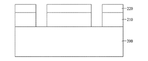
[0002] メモリデバイス、論理デバイス、マイクロプロセッサなどの半導体デバイスの形成は、ハードマスクの形成を含む。ハードマスクは、エッチングされる下位の基板上にブランケット層として形成される。フォトレジストのパターニングされた層は、パターンとしてフォトレジスト層を用いてハードマスクがエッチングされる前に、ハードマスクの上に形成される。ハードマスクが下位の基板をエッチングするためのソロパターンとして残るように、ハードマスクのパターニング後、フォトレジスト層は除去される。ハードマスクは下位の基板上に形成され、エッチングされ、次に基板から除去される別個の層であるが、エッチング処理に対する耐性が改善されていることに加えて、コストが安いため、ハードマスクを望ましいものにしている。ホウ素がドープされた炭素及び炭化ホウ素の膜は一般的に、パターニング性能が優れているため、高品質のハードマスクを生成することが知られている。
2BC + 5H2O → B2O3 + 2CO + 5H2 ………(i)
2BC + 7H2O → B2O3 + 2CO2 + 7H2 ……(ii)
三酸化ホウ素(B2O3)は次に過剰な蒸気と反応して、化学反応式(iii)及び(iv)に示したように、ホウ酸(H3BO3)及びメタホウ酸(HBO2)を産生する。
B2O3 + H2O → 2HBO2 …………………………… (iii)
B2O3 + 3H2O → 2H3BO3 ………………………… (iv)
ホウ酸及びメタホウ酸は揮発性の生成物である。ホウ酸及びメタホウ酸は水素ガス、一酸化炭素及び二酸化炭素と混合して、炭化ホウ素と水蒸気との間の反応生成物の気体混合物を形成する。
Claims (18)
- 基板の上に堆積した炭化ホウ素層をストリッピングする方法であって、
前記炭化ホウ素層が上部に堆積している前記基板を圧力容器の処理領域に装填することと、
500Torrから60barの圧力で、酸化剤を含む処理ガスであって、プラズマを含まない処理ガスに前記基板を曝露することと、
前記処理ガスの凝結点を超える温度まで前記圧力容器の前記処理領域を加熱することと、
前記処理ガスと前記炭化ホウ素層との間の一又は複数の反応生成物を前記圧力容器から除去することと、
を含む方法。 - 前記基板を前記処理ガスに曝露することは、
前記基板を10barを超える圧力で蒸気に曝露することを含む、請求項1に記載の方法。 - 前記酸化剤は、オゾン、酸素、水蒸気、重水、アンモニア、過酸化物、水酸化物含有化合物、酸素同位体及び水素同位体からなる群から選択される、請求項1に記載の方法。
- 前記基板は、前記基板上に堆積した炭化ホウ素の量と完全に反応するのに必要な量の酸化剤を超える量の酸化剤に曝露される、請求項1に記載の方法。
- 前記圧力容器の前記処理領域は、300°Cから700°Cの温度まで加熱される、請求項1に記載の方法。
- 前記処理ガスは、5%の乾燥蒸気から100%の乾燥蒸気を含む、請求項1に記載の方法。
- 複数の基板の上に堆積した炭化ホウ素層をストリッピングする方法であって、
上部に堆積した前記炭化ホウ素層をそれぞれ有する前記複数の基板を、圧力容器の処理領域に同時に装填することと、
500Torrから60barの圧力で、酸化剤を含む処理ガスに前記複数の基板を曝露することと、
前記処理ガスの凝結点を超える温度まで前記圧力容器の前記処理領域を加熱することと、
前記処理ガスと前記炭化ホウ素層との間の一又は複数の反応生成物を前記圧力容器から除去することと、
を含む方法。 - 前記複数の基板を前記処理ガスに曝露することは、
前記複数の基板を10barを超える圧力で蒸気に曝露することを含む、請求項7に記載の方法。 - 前記酸化剤は、オゾン、酸素、水蒸気、重水、アンモニア、過酸化物、水酸化物含有化合物、酸素同位体及び水素同位体からなる群から選択される、請求項7に記載の方法。
- 前記複数の基板は、前記複数の基板上に堆積した炭化ホウ素の量と完全に反応するのに必要な量の酸化剤を超える量の酸化剤に曝露される、請求項7に記載の方法。
- 前記圧力容器の前記処理領域は、300°Cから700°Cの温度まで加熱される、請求項7に記載の方法。
- 前記処理ガスは、5%の乾燥蒸気から100%の乾燥蒸気を含む、請求項7に記載の方法。
- 複数の基板の上に堆積した炭化ホウ素層をストリッピングする方法であって、
上部に堆積した前記炭化ホウ素層をそれぞれ有する前記複数の基板を、圧力容器の処理領域に同時に装填することと、
10barから60barの圧力で、蒸気を含む処理ガスに前記複数の基板を曝露することと、
前記処理ガスの凝結点を超える温度まで前記圧力容器の前記処理領域を加熱することと、
前記処理ガスと前記炭化ホウ素層との間の一又は複数の反応生成物を前記圧力容器から除去することと、
を含む方法。 - 前記処理ガスは、5%の過熱蒸気から100%の過熱蒸気を含む、請求項13に記載の方法。
- 前記酸化剤は、過酸化水素である、請求項3に記載の方法。
- 前記一又は複数の反応生成物は、三酸化ホウ素、二酸化炭素、一酸化炭素、水素、ホウ酸及びメタホウ酸を含む、請求項1に記載の方法。
- 前記酸化剤は、過酸化水素である、請求項9に記載の方法。
- 前記一又は複数の反応生成物は、三酸化ホウ素、二酸化炭素、一酸化炭素、水素、ホウ酸及びメタホウ酸を含む、請求項7に記載の方法。
Applications Claiming Priority (5)
| Application Number | Priority Date | Filing Date | Title |
|---|---|---|---|
| US201762514554P | 2017-06-02 | 2017-06-02 | |
| US62/514,554 | 2017-06-02 | ||
| US201862648073P | 2018-03-26 | 2018-03-26 | |
| US62/648,073 | 2018-03-26 | ||
| PCT/US2018/035210 WO2018222771A1 (en) | 2017-06-02 | 2018-05-30 | Dry stripping of boron carbide hardmask |
Publications (3)
| Publication Number | Publication Date |
|---|---|
| JP2020522882A JP2020522882A (ja) | 2020-07-30 |
| JP2020522882A5 JP2020522882A5 (ja) | 2021-07-26 |
| JP7190450B2 true JP7190450B2 (ja) | 2022-12-15 |
Family
ID=64455587
Family Applications (1)
| Application Number | Title | Priority Date | Filing Date |
|---|---|---|---|
| JP2019564959A Active JP7190450B2 (ja) | 2017-06-02 | 2018-05-30 | 炭化ホウ素ハードマスクのドライストリッピング |
Country Status (6)
| Country | Link |
|---|---|
| US (1) | US10529585B2 (ja) |
| JP (1) | JP7190450B2 (ja) |
| KR (1) | KR102574914B1 (ja) |
| CN (1) | CN110678973B (ja) |
| TW (1) | TWI763858B (ja) |
| WO (1) | WO2018222771A1 (ja) |
Families Citing this family (16)
| Publication number | Priority date | Publication date | Assignee | Title |
|---|---|---|---|---|
| US10622214B2 (en) | 2017-05-25 | 2020-04-14 | Applied Materials, Inc. | Tungsten defluorination by high pressure treatment |
| CN111095513B (zh) | 2017-08-18 | 2023-10-31 | 应用材料公司 | 高压高温退火腔室 |
| US10276411B2 (en) | 2017-08-18 | 2019-04-30 | Applied Materials, Inc. | High pressure and high temperature anneal chamber |
| KR102659317B1 (ko) | 2017-09-12 | 2024-04-18 | 어플라이드 머티어리얼스, 인코포레이티드 | 보호 배리어 층을 사용하여 반도체 구조들을 제조하기 위한 장치 및 방법들 |
| KR102396319B1 (ko) | 2017-11-11 | 2022-05-09 | 마이크로머티어리얼즈 엘엘씨 | 고압 프로세싱 챔버를 위한 가스 전달 시스템 |
| KR20200075892A (ko) | 2017-11-17 | 2020-06-26 | 어플라이드 머티어리얼스, 인코포레이티드 | 고압 처리 시스템을 위한 컨덴서 시스템 |
| EP3762962A4 (en) | 2018-03-09 | 2021-12-08 | Applied Materials, Inc. | HIGH PRESSURE ANNEALING PROCESS FOR METAL-BASED MATERIALS |
| US10950429B2 (en) | 2018-05-08 | 2021-03-16 | Applied Materials, Inc. | Methods of forming amorphous carbon hard mask layers and hard mask layers formed therefrom |
| CN112385125A (zh) * | 2018-07-09 | 2021-02-19 | 西门子能源美国公司 | 超临界co2冷却的电机 |
| US10748783B2 (en) | 2018-07-25 | 2020-08-18 | Applied Materials, Inc. | Gas delivery module |
| WO2020117462A1 (en) | 2018-12-07 | 2020-06-11 | Applied Materials, Inc. | Semiconductor processing system |
| CN113130384A (zh) * | 2020-01-16 | 2021-07-16 | 中芯国际集成电路制造(天津)有限公司 | 半导体结构的形成方法 |
| US11901222B2 (en) | 2020-02-17 | 2024-02-13 | Applied Materials, Inc. | Multi-step process for flowable gap-fill film |
| US11600507B2 (en) * | 2020-09-09 | 2023-03-07 | Applied Materials, Inc. | Pedestal assembly for a substrate processing chamber |
| US20220230887A1 (en) * | 2021-01-15 | 2022-07-21 | Applied Materials, Inc. | Methods and apparatus for processing a substrate |
| KR20240053429A (ko) * | 2022-10-17 | 2024-04-24 | 피에스케이 주식회사 | 기판 처리 장치 및 기판 처리 방법 |
Citations (4)
| Publication number | Priority date | Publication date | Assignee | Title |
|---|---|---|---|---|
| JP2009515366A (ja) | 2005-11-08 | 2009-04-09 | 東京エレクトロン株式会社 | バッチ式フォトレジスト乾式剥離・アッシングシステム及び方法 |
| JP2014516205A (ja) | 2011-05-12 | 2014-07-07 | アプライド マテリアルズ インコーポレイテッド | ホウ素炭素膜をドライストリッピングする方法 |
| US20140216498A1 (en) | 2013-02-06 | 2014-08-07 | Kwangduk Douglas Lee | Methods of dry stripping boron-carbon films |
| JP2018511166A (ja) | 2015-04-02 | 2018-04-19 | アプライド マテリアルズ インコーポレイテッドApplied Materials,Incorporated | パターニングのためのマスクエッチング |
Family Cites Families (200)
| Publication number | Priority date | Publication date | Assignee | Title |
|---|---|---|---|---|
| US4524587A (en) | 1967-01-10 | 1985-06-25 | Kantor Frederick W | Rotary thermodynamic apparatus and method |
| JPH0748489B2 (ja) | 1987-07-27 | 1995-05-24 | 富士通株式会社 | プラズマ処理装置 |
| US5114513A (en) | 1988-10-27 | 1992-05-19 | Omron Tateisi Electronics Co. | Optical device and manufacturing method thereof |
| JP2730695B2 (ja) | 1989-04-10 | 1998-03-25 | 忠弘 大見 | タングステン膜の成膜装置 |
| US5175123A (en) | 1990-11-13 | 1992-12-29 | Motorola, Inc. | High-pressure polysilicon encapsulated localized oxidation of silicon |
| US5050540A (en) | 1991-01-29 | 1991-09-24 | Arne Lindberg | Method of gas blanketing a boiler |
| JPH05139870A (ja) * | 1991-11-25 | 1993-06-08 | Hitachi Chem Co Ltd | 炭化硼素被覆炭素材料 |
| US5319212A (en) | 1992-10-07 | 1994-06-07 | Genus, Inc. | Method of monitoring ion beam current in ion implantation apparatus for use in manufacturing semiconductors |
| US5607002A (en) | 1993-04-28 | 1997-03-04 | Advanced Delivery & Chemical Systems, Inc. | Chemical refill system for high purity chemicals |
| JPH0733565A (ja) * | 1993-07-20 | 1995-02-03 | Toyo Tanso Kk | 炭化ホウ素被覆炭素材料及びその製造方法 |
| US5880041A (en) | 1994-05-27 | 1999-03-09 | Motorola Inc. | Method for forming a dielectric layer using high pressure |
| US5620524A (en) | 1995-02-27 | 1997-04-15 | Fan; Chiko | Apparatus for fluid delivery in chemical vapor deposition systems |
| US5858051A (en) | 1995-05-08 | 1999-01-12 | Toshiba Machine Co., Ltd. | Method of manufacturing optical waveguide |
| US5895274A (en) | 1996-01-22 | 1999-04-20 | Micron Technology, Inc. | High-pressure anneal process for integrated circuits |
| KR980012044A (ko) | 1996-03-01 | 1998-04-30 | 히가시 데츠로 | 기판건조장치 및 기판건조방법 |
| US5998305A (en) * | 1996-03-29 | 1999-12-07 | Praxair Technology, Inc. | Removal of carbon from substrate surfaces |
| US5738915A (en) | 1996-09-19 | 1998-04-14 | Lambda Technologies, Inc. | Curing polymer layers on semiconductor substrates using variable frequency microwave energy |
| US6444037B1 (en) | 1996-11-13 | 2002-09-03 | Applied Materials, Inc. | Chamber liner for high temperature processing chamber |
| US6082950A (en) | 1996-11-18 | 2000-07-04 | Applied Materials, Inc. | Front end wafer staging with wafer cassette turntables and on-the-fly wafer center finding |
| US6136664A (en) | 1997-08-07 | 2000-10-24 | International Business Machines Corporation | Filling of high aspect ratio trench isolation |
| US5963817A (en) | 1997-10-16 | 1999-10-05 | International Business Machines Corporation | Bulk and strained silicon on insulator using local selective oxidation |
| JP3199006B2 (ja) | 1997-11-18 | 2001-08-13 | 日本電気株式会社 | 層間絶縁膜の形成方法および絶縁膜形成装置 |
| US6442980B2 (en) | 1997-11-26 | 2002-09-03 | Chart Inc. | Carbon dioxide dry cleaning system |
| JPH11171669A (ja) * | 1997-12-15 | 1999-06-29 | Ngk Insulators Ltd | 炭化硼素皮膜の製造方法 |
| US6846739B1 (en) | 1998-02-27 | 2005-01-25 | Micron Technology, Inc. | MOCVD process using ozone as a reactant to deposit a metal oxide barrier layer |
| US6719516B2 (en) | 1998-09-28 | 2004-04-13 | Applied Materials, Inc. | Single wafer load lock with internal wafer transport |
| US20030101938A1 (en) | 1998-10-27 | 2003-06-05 | Applied Materials, Inc. | Apparatus for the deposition of high dielectric constant films |
| US6612317B2 (en) | 2000-04-18 | 2003-09-02 | S.C. Fluids, Inc | Supercritical fluid delivery and recovery system for semiconductor wafer processing |
| US6334266B1 (en) | 1999-09-20 | 2002-01-01 | S.C. Fluids, Inc. | Supercritical fluid drying system and method of use |
| EP1077477B1 (en) | 1999-08-17 | 2008-12-17 | Applied Materials, Inc. | Surface treatment of C-doped SiO2 film to enhance film stability during O2 ashing |
| US6299753B1 (en) | 1999-09-01 | 2001-10-09 | Applied Materials, Inc. | Double pressure vessel chemical dispenser unit |
| US6500603B1 (en) | 1999-11-11 | 2002-12-31 | Mitsui Chemicals, Inc. | Method for manufacturing polymer optical waveguide |
| US6150286A (en) | 2000-01-03 | 2000-11-21 | Advanced Micro Devices, Inc. | Method of making an ultra thin silicon nitride film |
| US6541367B1 (en) | 2000-01-18 | 2003-04-01 | Applied Materials, Inc. | Very low dielectric constant plasma-enhanced CVD films |
| US6319766B1 (en) | 2000-02-22 | 2001-11-20 | Applied Materials, Inc. | Method of tantalum nitride deposition by tantalum oxide densification |
| JP2001250787A (ja) | 2000-03-06 | 2001-09-14 | Hitachi Kokusai Electric Inc | 基板処理装置および基板処理方法 |
| US20040025908A1 (en) | 2000-04-18 | 2004-02-12 | Stephen Douglas | Supercritical fluid delivery system for semiconductor wafer processing |
| US7166524B2 (en) | 2000-08-11 | 2007-01-23 | Applied Materials, Inc. | Method for ion implanting insulator material to reduce dielectric constant |
| US6852167B2 (en) | 2001-03-01 | 2005-02-08 | Micron Technology, Inc. | Methods, systems, and apparatus for uniform chemical-vapor depositions |
| US6797336B2 (en) | 2001-03-22 | 2004-09-28 | Ambp Tech Corporation | Multi-component substances and processes for preparation thereof |
| TW544797B (en) | 2001-04-17 | 2003-08-01 | Kobe Steel Ltd | High-pressure processing apparatus |
| US7080651B2 (en) | 2001-05-17 | 2006-07-25 | Dainippon Screen Mfg. Co., Ltd. | High pressure processing apparatus and method |
| EP1271636A1 (en) | 2001-06-22 | 2003-01-02 | Infineon Technologies AG | Thermal oxidation process control by controlling oxidation agent partial pressure |
| US6781801B2 (en) | 2001-08-10 | 2004-08-24 | Seagate Technology Llc | Tunneling magnetoresistive sensor with spin polarized current injection |
| US6619304B2 (en) | 2001-09-13 | 2003-09-16 | Micell Technologies, Inc. | Pressure chamber assembly including non-mechanical drive means |
| US20030098069A1 (en) | 2001-11-26 | 2003-05-29 | Sund Wesley E. | High purity fluid delivery system |
| US6848458B1 (en) | 2002-02-05 | 2005-02-01 | Novellus Systems, Inc. | Apparatus and methods for processing semiconductor substrates using supercritical fluids |
| US6632325B2 (en) | 2002-02-07 | 2003-10-14 | Applied Materials, Inc. | Article for use in a semiconductor processing chamber and method of fabricating same |
| US7589029B2 (en) * | 2002-05-02 | 2009-09-15 | Micron Technology, Inc. | Atomic layer deposition and conversion |
| US7638727B2 (en) | 2002-05-08 | 2009-12-29 | Btu International Inc. | Plasma-assisted heat treatment |
| US7521089B2 (en) | 2002-06-13 | 2009-04-21 | Tokyo Electron Limited | Method and apparatus for controlling the movement of CVD reaction byproduct gases to adjacent process chambers |
| US20070243317A1 (en) | 2002-07-15 | 2007-10-18 | Du Bois Dale R | Thermal Processing System and Configurable Vertical Chamber |
| US20070212850A1 (en) | 2002-09-19 | 2007-09-13 | Applied Materials, Inc. | Gap-fill depositions in the formation of silicon containing dielectric materials |
| US7335609B2 (en) | 2004-08-27 | 2008-02-26 | Applied Materials, Inc. | Gap-fill depositions introducing hydroxyl-containing precursors in the formation of silicon containing dielectric materials |
| JP2004127958A (ja) | 2002-09-30 | 2004-04-22 | Kyoshin Engineering:Kk | 高圧アニール水蒸気処理を行なう装置及び方法 |
| US20040060519A1 (en) | 2002-10-01 | 2004-04-01 | Seh America Inc. | Quartz to quartz seal using expanded PTFE gasket material |
| US6889508B2 (en) | 2002-10-02 | 2005-05-10 | The Boc Group, Inc. | High pressure CO2 purification and supply system |
| US20040112409A1 (en) | 2002-12-16 | 2004-06-17 | Supercritical Sysems, Inc. | Fluoride in supercritical fluid for photoresist and residue removal |
| EP1597752A2 (en) | 2003-02-04 | 2005-11-23 | Applied Materials, Inc. | Tailoring nitrogen profile in silicon oxynitride using rapid thermal annealing with ammonia under ultra-low pressure |
| JP3956049B2 (ja) | 2003-03-07 | 2007-08-08 | 東京エレクトロン株式会社 | タングステン膜の形成方法 |
| US6939794B2 (en) | 2003-06-17 | 2005-09-06 | Micron Technology, Inc. | Boron-doped amorphous carbon film for use as a hard etch mask during the formation of a semiconductor device |
| WO2005007283A2 (en) | 2003-07-08 | 2005-01-27 | Sundew Technologies, Llc | Apparatus and method for downstream pressure control and sub-atmospheric reactive gas abatement |
| JP4173781B2 (ja) | 2003-08-13 | 2008-10-29 | 株式会社神戸製鋼所 | 高圧処理方法 |
| US20050136684A1 (en) | 2003-12-23 | 2005-06-23 | Applied Materials, Inc. | Gap-fill techniques |
| US7158221B2 (en) | 2003-12-23 | 2007-01-02 | Applied Materials, Inc. | Method and apparatus for performing limited area spectral analysis |
| US20050250347A1 (en) | 2003-12-31 | 2005-11-10 | Bailey Christopher M | Method and apparatus for maintaining by-product volatility in deposition process |
| US7030468B2 (en) | 2004-01-16 | 2006-04-18 | International Business Machines Corporation | Low k and ultra low k SiCOH dielectric films and methods to form the same |
| US20050187647A1 (en) | 2004-02-19 | 2005-08-25 | Kuo-Hua Wang | Intelligent full automation controlled flow for a semiconductor furnace tool |
| JP4393268B2 (ja) | 2004-05-20 | 2010-01-06 | 株式会社神戸製鋼所 | 微細構造体の乾燥方法 |
| US20050269291A1 (en) | 2004-06-04 | 2005-12-08 | Tokyo Electron Limited | Method of operating a processing system for treating a substrate |
| US7521378B2 (en) | 2004-07-01 | 2009-04-21 | Micron Technology, Inc. | Low temperature process for polysilazane oxidation/densification |
| US7491658B2 (en) | 2004-10-13 | 2009-02-17 | International Business Machines Corporation | Ultra low k plasma enhanced chemical vapor deposition processes using a single bifunctional precursor containing both a SiCOH matrix functionality and organic porogen functionality |
| US20060156979A1 (en) | 2004-11-22 | 2006-07-20 | Applied Materials, Inc. | Substrate processing apparatus using a batch processing chamber |
| JP5531284B2 (ja) | 2005-02-22 | 2014-06-25 | エスピーティーエス テクノロジーズ リミテッド | 副チャンバアセンブリを備えるエッチング用チャンバ |
| WO2006101315A1 (en) | 2005-03-21 | 2006-09-28 | Pkl Co., Ltd. | Device and method for cleaning photomask |
| US20060226117A1 (en) | 2005-03-29 | 2006-10-12 | Bertram Ronald T | Phase change based heating element system and method |
| US20120060868A1 (en) | 2005-06-07 | 2012-03-15 | Donald Gray | Microscale fluid delivery system |
| ES2317159T3 (es) | 2005-06-10 | 2009-04-16 | Obducat Ab | Replicacion de modelo con sello intermedio. |
| JP4747693B2 (ja) | 2005-06-28 | 2011-08-17 | 住友電気工業株式会社 | 樹脂体を形成する方法、光導波路のための構造を形成する方法、および光学部品を形成する方法 |
| US7361231B2 (en) | 2005-07-01 | 2008-04-22 | Ekc Technology, Inc. | System and method for mid-pressure dense phase gas and ultrasonic cleaning |
| US8148271B2 (en) | 2005-08-05 | 2012-04-03 | Hitachi Kokusai Electric Inc. | Substrate processing apparatus, coolant gas supply nozzle and semiconductor device manufacturing method |
| US7534080B2 (en) | 2005-08-26 | 2009-05-19 | Ascentool, Inc. | Vacuum processing and transfer system |
| KR100696178B1 (ko) | 2005-09-13 | 2007-03-20 | 한국전자통신연구원 | 광 도파로 마스터 및 그 제조 방법 |
| US8926731B2 (en) | 2005-09-13 | 2015-01-06 | Rasirc | Methods and devices for producing high purity steam |
| CN101268012B (zh) | 2005-10-07 | 2012-12-26 | 株式会社尼康 | 微小构造体及其制造方法 |
| US20070187386A1 (en) | 2006-02-10 | 2007-08-16 | Poongsan Microtec Corporation | Methods and apparatuses for high pressure gas annealing |
| US7578258B2 (en) | 2006-03-03 | 2009-08-25 | Lam Research Corporation | Methods and apparatus for selective pre-coating of a plasma processing chamber |
| JP2007242791A (ja) | 2006-03-07 | 2007-09-20 | Hitachi Kokusai Electric Inc | 基板処理装置 |
| US8062408B2 (en) | 2006-05-08 | 2011-11-22 | The Board Of Trustees Of The University Of Illinois | Integrated vacuum absorption steam cycle gas separation |
| US7825038B2 (en) | 2006-05-30 | 2010-11-02 | Applied Materials, Inc. | Chemical vapor deposition of high quality flow-like silicon dioxide using a silicon containing precursor and atomic oxygen |
| US20080169183A1 (en) | 2007-01-16 | 2008-07-17 | Varian Semiconductor Equipment Associates, Inc. | Plasma Source with Liner for Reducing Metal Contamination |
| JP2008192642A (ja) | 2007-01-31 | 2008-08-21 | Tokyo Electron Ltd | 基板処理装置 |
| US20080233404A1 (en) | 2007-03-22 | 2008-09-25 | 3M Innovative Properties Company | Microreplication tools and patterns using laser induced thermal embossing |
| JP5135856B2 (ja) | 2007-03-31 | 2013-02-06 | 東京エレクトロン株式会社 | トラップ装置、排気系及びこれを用いた処理システム |
| KR101442238B1 (ko) | 2007-07-26 | 2014-09-23 | 주식회사 풍산마이크로텍 | 고압 산소 열처리를 통한 반도체 소자의 제조방법 |
| US7951728B2 (en) | 2007-09-24 | 2011-05-31 | Applied Materials, Inc. | Method of improving oxide growth rate of selective oxidation processes |
| US7803722B2 (en) | 2007-10-22 | 2010-09-28 | Applied Materials, Inc | Methods for forming a dielectric layer within trenches |
| US7867923B2 (en) | 2007-10-22 | 2011-01-11 | Applied Materials, Inc. | High quality silicon oxide films by remote plasma CVD from disilane precursors |
| US7541297B2 (en) | 2007-10-22 | 2009-06-02 | Applied Materials, Inc. | Method and system for improving dielectric film quality for void free gap fill |
| US7651959B2 (en) | 2007-12-03 | 2010-01-26 | Asm Japan K.K. | Method for forming silazane-based dielectric film |
| US7776740B2 (en) | 2008-01-22 | 2010-08-17 | Tokyo Electron Limited | Method for integrating selective low-temperature ruthenium deposition into copper metallization of a semiconductor device |
| JP4815464B2 (ja) | 2008-03-31 | 2011-11-16 | 株式会社日立製作所 | 微細構造転写スタンパ及び微細構造転写装置 |
| US7655532B1 (en) | 2008-07-25 | 2010-02-02 | Taiwan Semiconductor Manufacturing Company, Ltd. | STI film property using SOD post-treatment |
| JP2010056541A (ja) | 2008-07-31 | 2010-03-11 | Semiconductor Energy Lab Co Ltd | 半導体装置およびその作製方法 |
| US8153533B2 (en) | 2008-09-24 | 2012-04-10 | Lam Research | Methods and systems for preventing feature collapse during microelectronic topography fabrication |
| US7891228B2 (en) | 2008-11-18 | 2011-02-22 | Mks Instruments, Inc. | Dual-mode mass flow verification and mass flow delivery system and method |
| US8557712B1 (en) | 2008-12-15 | 2013-10-15 | Novellus Systems, Inc. | PECVD flowable dielectric gap fill |
| JP2010205854A (ja) | 2009-03-02 | 2010-09-16 | Fujitsu Semiconductor Ltd | 半導体装置の製造方法 |
| US20100304027A1 (en) | 2009-05-27 | 2010-12-02 | Applied Materials, Inc. | Substrate processing system and methods thereof |
| JP4415062B1 (ja) | 2009-06-22 | 2010-02-17 | 富士フイルム株式会社 | 薄膜トランジスタ及び薄膜トランジスタの製造方法 |
| KR20110000960A (ko) | 2009-06-29 | 2011-01-06 | 삼성전자주식회사 | 반도체 칩, 스택 모듈, 메모리 카드 및 그 제조 방법 |
| US8741788B2 (en) | 2009-08-06 | 2014-06-03 | Applied Materials, Inc. | Formation of silicon oxide using non-carbon flowable CVD processes |
| JP2011066100A (ja) | 2009-09-16 | 2011-03-31 | Bridgestone Corp | 光硬化性転写シート、及びこれを用いた凹凸パターンの形成方法 |
| US8449942B2 (en) | 2009-11-12 | 2013-05-28 | Applied Materials, Inc. | Methods of curing non-carbon flowable CVD films |
| WO2011062043A1 (en) | 2009-11-20 | 2011-05-26 | Semiconductor Energy Laboratory Co., Ltd. | Method for manufacturing semiconductor device |
| US20110151677A1 (en) | 2009-12-21 | 2011-06-23 | Applied Materials, Inc. | Wet oxidation process performed on a dielectric material formed from a flowable cvd process |
| CN102754193A (zh) | 2010-01-06 | 2012-10-24 | 应用材料公司 | 使用氧化物衬垫的可流动电介质 |
| SG182333A1 (en) | 2010-01-07 | 2012-08-30 | Applied Materials Inc | In-situ ozone cure for radical-component cvd |
| KR101775608B1 (ko) | 2010-01-21 | 2017-09-19 | 파워다인, 인코포레이티드 | 탄소질 물질로부터의 스팀의 발생 방법 |
| US8293658B2 (en) | 2010-02-17 | 2012-10-23 | Asm America, Inc. | Reactive site deactivation against vapor deposition |
| JP2013521650A (ja) | 2010-03-05 | 2013-06-10 | アプライド マテリアルズ インコーポレイテッド | ラジカル成分cvdによる共形層 |
| CN101871043B (zh) | 2010-06-25 | 2012-07-18 | 东莞市康汇聚线材科技有限公司 | 一种退火炉蒸汽发生器及其控制方法 |
| US8318584B2 (en) | 2010-07-30 | 2012-11-27 | Applied Materials, Inc. | Oxide-rich liner layer for flowable CVD gapfill |
| JP2012049446A (ja) | 2010-08-30 | 2012-03-08 | Toshiba Corp | 超臨界乾燥方法及び超臨界乾燥システム |
| EP2426720A1 (en) | 2010-09-03 | 2012-03-07 | Applied Materials, Inc. | Staggered thin film transistor and method of forming the same |
| TW201216331A (en) | 2010-10-05 | 2012-04-16 | Applied Materials Inc | Ultra high selectivity doped amorphous carbon strippable hardmask development and integration |
| JP5806827B2 (ja) | 2011-03-18 | 2015-11-10 | 東京エレクトロン株式会社 | ゲートバルブ装置及び基板処理装置並びにその基板処理方法 |
| JP5450494B2 (ja) | 2011-03-25 | 2014-03-26 | 株式会社東芝 | 半導体基板の超臨界乾燥方法 |
| CN103502853A (zh) | 2011-03-25 | 2014-01-08 | 李谞荣 | 光波电路及其制造方法 |
| JP6048400B2 (ja) | 2011-03-30 | 2016-12-21 | 大日本印刷株式会社 | 超臨界乾燥装置及び超臨界乾燥方法 |
| US20120252210A1 (en) | 2011-03-30 | 2012-10-04 | Tokyo Electron Limited | Method for modifying metal cap layers in semiconductor devices |
| US9653327B2 (en) | 2011-05-12 | 2017-05-16 | Applied Materials, Inc. | Methods of removing a material layer from a substrate using water vapor treatment |
| US8466073B2 (en) | 2011-06-03 | 2013-06-18 | Applied Materials, Inc. | Capping layer for reduced outgassing |
| GB201110117D0 (en) | 2011-06-16 | 2011-07-27 | Fujifilm Mfg Europe Bv | method and device for manufacturing a barrie layer on a flexible substrate |
| US9029228B2 (en) * | 2011-10-19 | 2015-05-12 | SunEdision Semiconductor Limited (UEN201334164H) | Direct and sequential formation of monolayers of boron nitride and graphene on substrates |
| JPWO2013065771A1 (ja) | 2011-11-01 | 2015-04-02 | 株式会社日立国際電気 | 半導体装置の製造方法、半導体装置の製造装置及び記録媒体 |
| JP2013122493A (ja) | 2011-12-09 | 2013-06-20 | Furukawa Electric Co Ltd:The | 光分岐素子および光分岐回路 |
| JP2013154315A (ja) | 2012-01-31 | 2013-08-15 | Ricoh Co Ltd | 薄膜形成装置、薄膜形成方法、電気−機械変換素子、液体吐出ヘッド、およびインクジェット記録装置 |
| US8993458B2 (en) | 2012-02-13 | 2015-03-31 | Applied Materials, Inc. | Methods and apparatus for selective oxidation of a substrate |
| US8871656B2 (en) | 2012-03-05 | 2014-10-28 | Applied Materials, Inc. | Flowable films using alternative silicon precursors |
| US20130337171A1 (en) | 2012-06-13 | 2013-12-19 | Qualcomm Mems Technologies, Inc. | N2 purged o-ring for chamber in chamber ald system |
| KR101224520B1 (ko) | 2012-06-27 | 2013-01-22 | (주)이노시티 | 프로세스 챔버 |
| KR20140003776A (ko) * | 2012-06-28 | 2014-01-10 | 주식회사 메카로닉스 | 고 저항 산화아연 박막의 제조방법 |
| WO2014011954A1 (en) | 2012-07-13 | 2014-01-16 | Northwestern University | Multifunctional graphene coated scanning tips |
| JP2014019912A (ja) | 2012-07-19 | 2014-02-03 | Tokyo Electron Ltd | タングステン膜の成膜方法 |
| US8846448B2 (en) | 2012-08-10 | 2014-09-30 | Taiwan Semiconductor Manufacturing Co., Ltd. | Warpage control in a package-on-package structure |
| WO2014030371A1 (ja) | 2012-08-24 | 2014-02-27 | 独立行政法人科学技術振興機構 | ゲルマニウム層上に窒化酸化アルミニウム膜を備える半導体構造およびその製造方法 |
| KR102002782B1 (ko) | 2012-09-10 | 2019-07-23 | 삼성전자주식회사 | 팽창성 부재를 사용하는 반도체 장치의 제조 방법 |
| JP2014060256A (ja) | 2012-09-18 | 2014-04-03 | Tokyo Electron Ltd | 処理システム |
| US9157730B2 (en) | 2012-10-26 | 2015-10-13 | Applied Materials, Inc. | PECVD process |
| SG2013083241A (en) | 2012-11-08 | 2014-06-27 | Novellus Systems Inc | Conformal film deposition for gapfill |
| US20150322286A1 (en) | 2012-11-27 | 2015-11-12 | The Regents Of The University Of California | Polymerized Metal-Organic Material for Printable Photonic Devices |
| JP2014141739A (ja) | 2012-12-27 | 2014-08-07 | Tokyo Electron Ltd | 金属マンガン膜の成膜方法、処理システム、電子デバイスの製造方法および電子デバイス |
| MY171887A (en) | 2013-02-19 | 2019-11-06 | Applied Materials Inc | Hdd patterning using flowable cvd film |
| KR101443792B1 (ko) | 2013-02-20 | 2014-09-26 | 국제엘렉트릭코리아 주식회사 | 건식 기상 식각 장치 |
| KR20140106977A (ko) | 2013-02-27 | 2014-09-04 | 삼성전자주식회사 | 고성능 금속 산화물 반도체 박막 트랜지스터 및 그 제조방법 |
| US9354508B2 (en) | 2013-03-12 | 2016-05-31 | Applied Materials, Inc. | Planarized extreme ultraviolet lithography blank, and manufacturing and lithography systems therefor |
| US9680095B2 (en) | 2013-03-13 | 2017-06-13 | Macronix International Co., Ltd. | Resistive RAM and fabrication method |
| US20140271097A1 (en) | 2013-03-15 | 2014-09-18 | Applied Materials, Inc. | Processing systems and methods for halide scavenging |
| US10224258B2 (en) | 2013-03-22 | 2019-03-05 | Applied Materials, Inc. | Method of curing thermoplastics with microwave energy |
| US10172189B2 (en) | 2013-04-26 | 2019-01-01 | Applied Materials, Inc. | Method and apparatus for microwave treatment of dielectric films |
| JP6068633B2 (ja) | 2013-05-31 | 2017-01-25 | 株式会社日立国際電気 | 基板処理装置、半導体装置の製造方法及び炉口蓋体 |
| JP6196481B2 (ja) | 2013-06-24 | 2017-09-13 | 株式会社荏原製作所 | 排ガス処理装置 |
| KR101542803B1 (ko) | 2013-07-09 | 2015-08-07 | 주식회사 네오세미텍 | 고온고압 송풍식 퍼지수단을 구비한 진공챔버 및 이를 이용한 세정방법 |
| US9178103B2 (en) | 2013-08-09 | 2015-11-03 | Tsmc Solar Ltd. | Apparatus and method for forming chalcogenide semiconductor absorber materials with sodium impurities |
| WO2015023404A1 (en) | 2013-08-16 | 2015-02-19 | Applied Materials, Inc. | Tungsten deposition with tungsten hexafluoride (wf6) etchback |
| US9548200B2 (en) | 2013-08-21 | 2017-01-17 | Applied Materials, Inc. | Variable frequency microwave (VFM) processes and applications in semiconductor thin film fabrications |
| JP6226648B2 (ja) | 2013-09-04 | 2017-11-08 | 昭和電工株式会社 | SiCエピタキシャルウェハの製造方法 |
| JP6129712B2 (ja) | 2013-10-24 | 2017-05-17 | 信越化学工業株式会社 | 過熱水蒸気処理装置 |
| US9406547B2 (en) | 2013-12-24 | 2016-08-02 | Intel Corporation | Techniques for trench isolation using flowable dielectric materials |
| CN103745978B (zh) | 2014-01-03 | 2016-08-17 | 京东方科技集团股份有限公司 | 显示装置、阵列基板及其制作方法 |
| US9257527B2 (en) | 2014-02-14 | 2016-02-09 | International Business Machines Corporation | Nanowire transistor structures with merged source/drain regions using auxiliary pillars |
| US9818603B2 (en) | 2014-03-06 | 2017-11-14 | Taiwan Semiconductor Manufacturing Company, Ltd. | Semiconductor devices and methods of manufacture thereof |
| KR101571715B1 (ko) | 2014-04-23 | 2015-11-25 | 주식회사 풍산 | 고압 열처리를 이용한 스핀 온 글래스 절연막 형성방법 |
| CN104047676A (zh) | 2014-06-14 | 2014-09-17 | 马根昌 | 改良式对冲消声器 |
| CN104089491B (zh) | 2014-07-03 | 2015-11-04 | 肇庆宏旺金属实业有限公司 | 退火炉的余热回收利用系统 |
| KR102287344B1 (ko) * | 2014-07-25 | 2021-08-06 | 삼성전자주식회사 | 하드마스크 조성물 및 이를 이용한 패턴의 형성방법 |
| US9257314B1 (en) | 2014-07-31 | 2016-02-09 | Poongsan Corporation | Methods and apparatuses for deuterium recovery |
| WO2016038664A1 (ja) | 2014-09-08 | 2016-03-17 | 三菱電機株式会社 | 半導体アニール装置 |
| US9773865B2 (en) | 2014-09-22 | 2017-09-26 | International Business Machines Corporation | Self-forming spacers using oxidation |
| US9362107B2 (en) | 2014-09-30 | 2016-06-07 | Applied Materials, Inc. | Flowable low-k dielectric gapfill treatment |
| US20160118391A1 (en) | 2014-10-22 | 2016-04-28 | SanDisk Technologies, Inc. | Deuterium anneal of semiconductor channels in a three-dimensional memory structure |
| KR102332415B1 (ko) | 2014-10-24 | 2021-12-01 | 버슘머트리얼즈 유에스, 엘엘씨 | 실리콘-함유 막을 증착시키기 위한 조성물 및 이를 사용하는 방법 |
| US9543141B2 (en) | 2014-12-09 | 2017-01-10 | Taiwan Semiconductor Manufacturing Co., Ltd | Method for curing flowable layer |
| WO2016130956A1 (en) | 2015-02-13 | 2016-08-18 | Alexander Otto | Multifilament superconducting wire with high resistance sleeves |
| KR101681190B1 (ko) | 2015-05-15 | 2016-12-02 | 세메스 주식회사 | 기판 건조 장치 및 방법 |
| US10945313B2 (en) | 2015-05-27 | 2021-03-09 | Applied Materials, Inc. | Methods and apparatus for a microwave batch curing process |
| US9646850B2 (en) | 2015-07-06 | 2017-05-09 | Globalfoundries Inc. | High-pressure anneal |
| US9484406B1 (en) | 2015-09-03 | 2016-11-01 | Applied Materials, Inc. | Method for fabricating nanowires for horizontal gate all around devices for semiconductor applications |
| US9716142B2 (en) | 2015-10-12 | 2017-07-25 | International Business Machines Corporation | Stacked nanowires |
| US9754840B2 (en) | 2015-11-16 | 2017-09-05 | Taiwan Semiconductor Manufacturing Company, Ltd. | Horizontal gate-all-around device having wrapped-around source and drain |
| US9633838B2 (en) | 2015-12-28 | 2017-04-25 | L'Air Liquide, Société Anonyme pour l'Etude et l'Exploitation des Procédés Georges Claude | Vapor deposition of silicon-containing films using penta-substituted disilanes |
| JP6856651B2 (ja) | 2016-01-05 | 2021-04-07 | アプライド マテリアルズ インコーポレイテッドApplied Materials,Incorporated | 半導体アプリケーション用の水平ゲートオールアラウンドデバイスのためのナノワイヤ製造方法 |
| US9570551B1 (en) | 2016-02-05 | 2017-02-14 | International Business Machines Corporation | Replacement III-V or germanium nanowires by unilateral confined epitaxial growth |
| JP6240695B2 (ja) | 2016-03-02 | 2017-11-29 | 株式会社日立国際電気 | 基板処理装置、半導体装置の製造方法及びプログラム |
| US11326253B2 (en) | 2016-04-27 | 2022-05-10 | Applied Materials, Inc. | Atomic layer deposition of protective coatings for semiconductor process chamber components |
| TWI680535B (zh) | 2016-06-14 | 2019-12-21 | 美商應用材料股份有限公司 | 金屬及含金屬化合物之氧化體積膨脹 |
| US9876019B1 (en) | 2016-07-13 | 2018-01-23 | Globalfoundries Singapore Pte. Ltd. | Integrated circuits with programmable memory and methods for producing the same |
| CN109791913A (zh) | 2016-09-30 | 2019-05-21 | 应用材料公司 | 形成自对准通孔的方法 |
| US10224224B2 (en) | 2017-03-10 | 2019-03-05 | Micromaterials, LLC | High pressure wafer processing systems and related methods |
-
2018
- 2018-05-30 JP JP2019564959A patent/JP7190450B2/ja active Active
- 2018-05-30 KR KR1020197036359A patent/KR102574914B1/ko active IP Right Grant
- 2018-05-30 WO PCT/US2018/035210 patent/WO2018222771A1/en active Application Filing
- 2018-05-30 CN CN201880035089.1A patent/CN110678973B/zh active Active
- 2018-05-31 TW TW107118593A patent/TWI763858B/zh active
- 2018-06-01 US US15/995,698 patent/US10529585B2/en active Active
Patent Citations (4)
| Publication number | Priority date | Publication date | Assignee | Title |
|---|---|---|---|---|
| JP2009515366A (ja) | 2005-11-08 | 2009-04-09 | 東京エレクトロン株式会社 | バッチ式フォトレジスト乾式剥離・アッシングシステム及び方法 |
| JP2014516205A (ja) | 2011-05-12 | 2014-07-07 | アプライド マテリアルズ インコーポレイテッド | ホウ素炭素膜をドライストリッピングする方法 |
| US20140216498A1 (en) | 2013-02-06 | 2014-08-07 | Kwangduk Douglas Lee | Methods of dry stripping boron-carbon films |
| JP2018511166A (ja) | 2015-04-02 | 2018-04-19 | アプライド マテリアルズ インコーポレイテッドApplied Materials,Incorporated | パターニングのためのマスクエッチング |
Also Published As
| Publication number | Publication date |
|---|---|
| KR20200004399A (ko) | 2020-01-13 |
| US20180350621A1 (en) | 2018-12-06 |
| CN110678973A (zh) | 2020-01-10 |
| TW201903837A (zh) | 2019-01-16 |
| JP2020522882A (ja) | 2020-07-30 |
| CN110678973B (zh) | 2023-09-19 |
| WO2018222771A1 (en) | 2018-12-06 |
| KR102574914B1 (ko) | 2023-09-04 |
| US10529585B2 (en) | 2020-01-07 |
| TWI763858B (zh) | 2022-05-11 |
Similar Documents
| Publication | Publication Date | Title |
|---|---|---|
| JP7190450B2 (ja) | 炭化ホウ素ハードマスクのドライストリッピング | |
| JP7184810B6 (ja) | 基板に堆積された膜の品質改善 | |
| US20180033643A1 (en) | Methods and apparatus for using alkyl amines for the selective removal of metal nitride | |
| JP5202372B2 (ja) | 成膜装置のメタル汚染低減方法、半導体装置の製造方法、記憶媒体及び成膜装置 | |
| US8372212B2 (en) | Supercritical drying method and apparatus for semiconductor substrates | |
| JP5682290B2 (ja) | 炭素含有薄膜のスリミング方法及び酸化装置 | |
| WO2019036145A2 (en) | HIGH PRESSURE AND HIGH TEMPERATURE RECOVERY CHAMBER | |
| TW201943075A (zh) | 製造熱穩定之低介電常數鰭式場效電晶體間隔物之方法 | |
| US6171104B1 (en) | Oxidation treatment method and apparatus | |
| US6667244B1 (en) | Method for etching sidewall polymer and other residues from the surface of semiconductor devices | |
| JP2023138317A (ja) | ガスクリーニング方法、半導体装置の製造方法、基板処理方法、プログラム及び基板処理装置 | |
| US10217627B2 (en) | Methods of non-destructive post tungsten etch residue removal | |
| JP2006041482A (ja) | 被処理体の酸化方法、酸化装置及び記憶媒体 | |
| US20220139693A1 (en) | Method of manufacturing semiconductor device, surface treatment method, substrate processing apparatus, and recording medium | |
| US20220298628A1 (en) | Nozzle Cleaning Method, Substrate Processing Method, Method of Manufacturing Semiconductor Device, Substrate Processing Apparatus and Non-transitory Computer-readable Recording Medium | |
| TW411526B (en) | Method and device for forming gate oxide layers | |
| WO1992006488A1 (en) | Vapor supplier and its control method | |
| JP2023506400A (ja) | 少なくとも1つの半導体基板を処理するための装置および方法 | |
| JP2003282553A (ja) | 基板処理装置 | |
| JPH04254328A (ja) | 半導体装置の製造方法 | |
| JP2006004985A (ja) | 基板処理装置 | |
| KR20030084032A (ko) | 반도체 제조 장치의 로드락 챔버 |
Legal Events
| Date | Code | Title | Description |
|---|---|---|---|
| A521 | Request for written amendment filed |
Free format text: JAPANESE INTERMEDIATE CODE: A523 Effective date: 20210527 |
|
| A621 | Written request for application examination |
Free format text: JAPANESE INTERMEDIATE CODE: A621 Effective date: 20210527 |
|
| A977 | Report on retrieval |
Free format text: JAPANESE INTERMEDIATE CODE: A971007 Effective date: 20220616 |
|
| A131 | Notification of reasons for refusal |
Free format text: JAPANESE INTERMEDIATE CODE: A131 Effective date: 20220705 |
|
| A521 | Request for written amendment filed |
Free format text: JAPANESE INTERMEDIATE CODE: A523 Effective date: 20220930 |
|
| TRDD | Decision of grant or rejection written | ||
| A01 | Written decision to grant a patent or to grant a registration (utility model) |
Free format text: JAPANESE INTERMEDIATE CODE: A01 Effective date: 20221108 |
|
| A61 | First payment of annual fees (during grant procedure) |
Free format text: JAPANESE INTERMEDIATE CODE: A61 Effective date: 20221205 |
|
| R150 | Certificate of patent or registration of utility model |
Ref document number: 7190450 Country of ref document: JP Free format text: JAPANESE INTERMEDIATE CODE: R150 |