JP2014165210A - モジュール基板 - Google Patents
モジュール基板 Download PDFInfo
- Publication number
- JP2014165210A JP2014165210A JP2013032450A JP2013032450A JP2014165210A JP 2014165210 A JP2014165210 A JP 2014165210A JP 2013032450 A JP2013032450 A JP 2013032450A JP 2013032450 A JP2013032450 A JP 2013032450A JP 2014165210 A JP2014165210 A JP 2014165210A
- Authority
- JP
- Japan
- Prior art keywords
- board
- sub
- external electrode
- substrate
- module substrate
- Prior art date
- Legal status (The legal status is an assumption and is not a legal conclusion. Google has not performed a legal analysis and makes no representation as to the accuracy of the status listed.)
- Pending
Links
Images


Classifications
-
- H—ELECTRICITY
- H05—ELECTRIC TECHNIQUES NOT OTHERWISE PROVIDED FOR
- H05K—PRINTED CIRCUITS; CASINGS OR CONSTRUCTIONAL DETAILS OF ELECTRIC APPARATUS; MANUFACTURE OF ASSEMBLAGES OF ELECTRICAL COMPONENTS
- H05K1/00—Printed circuits
- H05K1/02—Details
- H05K1/14—Structural association of two or more printed circuits
- H05K1/144—Stacked arrangements of planar printed circuit boards
-
- H—ELECTRICITY
- H05—ELECTRIC TECHNIQUES NOT OTHERWISE PROVIDED FOR
- H05K—PRINTED CIRCUITS; CASINGS OR CONSTRUCTIONAL DETAILS OF ELECTRIC APPARATUS; MANUFACTURE OF ASSEMBLAGES OF ELECTRICAL COMPONENTS
- H05K1/00—Printed circuits
- H05K1/02—Details
- H05K1/11—Printed elements for providing electric connections to or between printed circuits
- H05K1/111—Pads for surface mounting, e.g. lay-out
-
- H—ELECTRICITY
- H05—ELECTRIC TECHNIQUES NOT OTHERWISE PROVIDED FOR
- H05K—PRINTED CIRCUITS; CASINGS OR CONSTRUCTIONAL DETAILS OF ELECTRIC APPARATUS; MANUFACTURE OF ASSEMBLAGES OF ELECTRICAL COMPONENTS
- H05K1/00—Printed circuits
- H05K1/02—Details
- H05K1/14—Structural association of two or more printed circuits
- H05K1/141—One or more single auxiliary printed circuits mounted on a main printed circuit, e.g. modules, adapters
-
- H—ELECTRICITY
- H10—SEMICONDUCTOR DEVICES; ELECTRIC SOLID-STATE DEVICES NOT OTHERWISE PROVIDED FOR
- H10W—GENERIC PACKAGES, INTERCONNECTIONS, CONNECTORS OR OTHER CONSTRUCTIONAL DETAILS OF DEVICES COVERED BY CLASS H10
- H10W90/00—Package configurations
- H10W90/401—Package configurations characterised by multiple insulating or insulated package substrates, interposers or RDLs
-
- H—ELECTRICITY
- H10—SEMICONDUCTOR DEVICES; ELECTRIC SOLID-STATE DEVICES NOT OTHERWISE PROVIDED FOR
- H10W—GENERIC PACKAGES, INTERCONNECTIONS, CONNECTORS OR OTHER CONSTRUCTIONAL DETAILS OF DEVICES COVERED BY CLASS H10
- H10W90/00—Package configurations
- H10W90/701—Package configurations characterised by the relative positions of pads or connectors relative to package parts
-
- H—ELECTRICITY
- H05—ELECTRIC TECHNIQUES NOT OTHERWISE PROVIDED FOR
- H05K—PRINTED CIRCUITS; CASINGS OR CONSTRUCTIONAL DETAILS OF ELECTRIC APPARATUS; MANUFACTURE OF ASSEMBLAGES OF ELECTRICAL COMPONENTS
- H05K2201/00—Indexing scheme relating to printed circuits covered by H05K1/00
- H05K2201/10—Details of components or other objects attached to or integrated in a printed circuit board
- H05K2201/10227—Other objects, e.g. metallic pieces
- H05K2201/10378—Interposers
-
- Y—GENERAL TAGGING OF NEW TECHNOLOGICAL DEVELOPMENTS; GENERAL TAGGING OF CROSS-SECTIONAL TECHNOLOGIES SPANNING OVER SEVERAL SECTIONS OF THE IPC; TECHNICAL SUBJECTS COVERED BY FORMER USPC CROSS-REFERENCE ART COLLECTIONS [XRACs] AND DIGESTS
- Y02—TECHNOLOGIES OR APPLICATIONS FOR MITIGATION OR ADAPTATION AGAINST CLIMATE CHANGE
- Y02P—CLIMATE CHANGE MITIGATION TECHNOLOGIES IN THE PRODUCTION OR PROCESSING OF GOODS
- Y02P70/00—Climate change mitigation technologies in the production process for final industrial or consumer products
- Y02P70/50—Manufacturing or production processes characterised by the final manufactured product
Landscapes
- Engineering & Computer Science (AREA)
- Microelectronics & Electronic Packaging (AREA)
- Combinations Of Printed Boards (AREA)
Priority Applications (2)
| Application Number | Priority Date | Filing Date | Title |
|---|---|---|---|
| JP2013032450A JP2014165210A (ja) | 2013-02-21 | 2013-02-21 | モジュール基板 |
| US14/184,958 US9468104B2 (en) | 2013-02-21 | 2014-02-20 | Module board |
Applications Claiming Priority (1)
| Application Number | Priority Date | Filing Date | Title |
|---|---|---|---|
| JP2013032450A JP2014165210A (ja) | 2013-02-21 | 2013-02-21 | モジュール基板 |
Publications (2)
| Publication Number | Publication Date |
|---|---|
| JP2014165210A true JP2014165210A (ja) | 2014-09-08 |
| JP2014165210A5 JP2014165210A5 (enExample) | 2016-04-07 |
Family
ID=51350999
Family Applications (1)
| Application Number | Title | Priority Date | Filing Date |
|---|---|---|---|
| JP2013032450A Pending JP2014165210A (ja) | 2013-02-21 | 2013-02-21 | モジュール基板 |
Country Status (2)
| Country | Link |
|---|---|
| US (1) | US9468104B2 (enExample) |
| JP (1) | JP2014165210A (enExample) |
Cited By (1)
| Publication number | Priority date | Publication date | Assignee | Title |
|---|---|---|---|---|
| JP2020512688A (ja) * | 2017-03-09 | 2020-04-23 | 華為技術有限公司Huawei Technologies Co.,Ltd. | 消費者向け電子製品のメインボードおよび端末 |
Families Citing this family (4)
| Publication number | Priority date | Publication date | Assignee | Title |
|---|---|---|---|---|
| US9363892B2 (en) * | 2013-07-19 | 2016-06-07 | Google Technology Holdings LLC | Circuit assembly and corresponding methods |
| DE102015220676A1 (de) * | 2015-10-22 | 2017-04-27 | Zf Friedrichshafen Ag | Leiterplatte und Anordnung mit einer Leiterplatte |
| DE102017206099A1 (de) * | 2017-04-10 | 2018-10-11 | BSH Hausgeräte GmbH | Leiterplatten-Anordnung sowie Verfahren zur Herstellung einer Leiterplatten-Anordnung |
| US11553616B2 (en) * | 2018-12-07 | 2023-01-10 | Delta Electronics, Inc. | Module with power device |
Citations (2)
| Publication number | Priority date | Publication date | Assignee | Title |
|---|---|---|---|---|
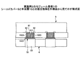
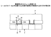
| JPH06111869A (ja) * | 1992-09-29 | 1994-04-22 | Fujitsu Ltd | 表面実装用端子 |
| JP2007066936A (ja) * | 2005-08-29 | 2007-03-15 | Matsushita Electric Ind Co Ltd | 高周波モジュールとその製造方法 |
Family Cites Families (35)
| Publication number | Priority date | Publication date | Assignee | Title |
|---|---|---|---|---|
| EP0732107A3 (en) * | 1995-03-16 | 1997-05-07 | Toshiba Kk | Shielding device for a circuit substrate |
| US6525414B2 (en) * | 1997-09-16 | 2003-02-25 | Matsushita Electric Industrial Co., Ltd. | Semiconductor device including a wiring board and semiconductor elements mounted thereon |
| US6137164A (en) * | 1998-03-16 | 2000-10-24 | Texas Instruments Incorporated | Thin stacked integrated circuit device |
| SG77652A1 (en) * | 1998-03-18 | 2001-01-16 | Hitachi Cable | Semiconductor device lead-patterning substrate and electronics device and method for fabricating same |
| JP2001167969A (ja) * | 1999-12-06 | 2001-06-22 | Tdk Corp | 三次元搭載用多端子積層セラミックコンデンサ |
| US6528870B2 (en) * | 2000-01-28 | 2003-03-04 | Kabushiki Kaisha Toshiba | Semiconductor device having a plurality of stacked wiring boards |
| EP1189282A4 (en) * | 2000-03-21 | 2006-02-15 | Mitsubishi Electric Corp | SEMICONDUCTOR ARRANGEMENT, METHOD FOR THE PRODUCTION OF ELECTRONIC SWITCHING, ELECTRONIC SWITCHING, AND PORTABLE INFORMATION TERMINAL |
| US6528408B2 (en) * | 2001-05-21 | 2003-03-04 | Micron Technology, Inc. | Method for bumped die and wire bonded board-on-chip package |
| US7087988B2 (en) * | 2002-07-30 | 2006-08-08 | Kabushiki Kaisha Toshiba | Semiconductor packaging apparatus |
| JP2004303944A (ja) | 2003-03-31 | 2004-10-28 | Matsushita Electric Ind Co Ltd | モジュール基板及びその製造方法 |
| PL200759B1 (pl) * | 2003-04-25 | 2009-02-27 | Adb Polska Sp | Zestaw płytek z obwodami drukowanymi |
| JP2005277355A (ja) * | 2004-03-26 | 2005-10-06 | Sanyo Electric Co Ltd | 回路装置 |
| JP2005286057A (ja) * | 2004-03-29 | 2005-10-13 | Sanyo Electric Co Ltd | 回路装置およびその製造方法 |
| JP4421436B2 (ja) * | 2004-09-30 | 2010-02-24 | 太陽誘電株式会社 | 面実装コイル部品 |
| JP4864419B2 (ja) * | 2005-10-28 | 2012-02-01 | 株式会社東芝 | プリント回路板および電子機器 |
| JP4740765B2 (ja) * | 2006-02-24 | 2011-08-03 | エルピーダメモリ株式会社 | 半導体装置及びその製造方法 |
| JP2007281276A (ja) * | 2006-04-10 | 2007-10-25 | Nec Electronics Corp | 半導体装置 |
| US20070241441A1 (en) * | 2006-04-17 | 2007-10-18 | Stats Chippac Ltd. | Multichip package system |
| JP2007294560A (ja) * | 2006-04-24 | 2007-11-08 | Nec Electronics Corp | 半導体装置およびその製造方法 |
| JP5154262B2 (ja) * | 2008-02-26 | 2013-02-27 | 太陽誘電株式会社 | 電子部品 |
| TWI362732B (en) * | 2008-04-07 | 2012-04-21 | Nanya Technology Corp | Multi-chip stack package |
| KR20100046760A (ko) * | 2008-10-28 | 2010-05-07 | 삼성전자주식회사 | 반도체 패키지 |
| CN102369600B (zh) * | 2009-04-02 | 2014-09-10 | 株式会社村田制作所 | 电路基板 |
| JP5234521B2 (ja) * | 2009-08-21 | 2013-07-10 | Tdk株式会社 | 電子部品及びその製造方法 |
| JP2011171427A (ja) * | 2010-02-17 | 2011-09-01 | Canon Inc | 積層型半導体装置 |
| US8847376B2 (en) * | 2010-07-23 | 2014-09-30 | Tessera, Inc. | Microelectronic elements with post-assembly planarization |
| JP2012079876A (ja) * | 2010-09-30 | 2012-04-19 | Fujitsu Ltd | 電子装置の製造方法及び電子装置 |
| JP2012104790A (ja) * | 2010-10-12 | 2012-05-31 | Elpida Memory Inc | 半導体装置 |
| JP5788166B2 (ja) * | 2010-11-02 | 2015-09-30 | 新光電気工業株式会社 | 接続端子構造及びその製造方法、並びにソケット |
| JP5360158B2 (ja) * | 2011-08-05 | 2013-12-04 | 株式会社村田製作所 | チップ部品構造体 |
| US8436457B2 (en) * | 2011-10-03 | 2013-05-07 | Invensas Corporation | Stub minimization for multi-die wirebond assemblies with parallel windows |
| JP5887414B2 (ja) * | 2011-10-03 | 2016-03-16 | インヴェンサス・コーポレイション | 平行な窓を有するマルチダイのワイヤボンドアセンブリのスタブ最小化 |
| US9462732B2 (en) * | 2013-03-13 | 2016-10-04 | Laird Technologies, Inc. | Electromagnetic interference shielding (EMI) apparatus including a frame with drawn latching features |
| JP6336714B2 (ja) * | 2013-05-27 | 2018-06-06 | 富士通コンポーネント株式会社 | 電子装置 |
| JP2015195263A (ja) * | 2014-03-31 | 2015-11-05 | マイクロン テクノロジー, インク. | 半導体装置及びその製造方法 |
-
2013
- 2013-02-21 JP JP2013032450A patent/JP2014165210A/ja active Pending
-
2014
- 2014-02-20 US US14/184,958 patent/US9468104B2/en not_active Expired - Fee Related
Patent Citations (2)
| Publication number | Priority date | Publication date | Assignee | Title |
|---|---|---|---|---|
| JPH06111869A (ja) * | 1992-09-29 | 1994-04-22 | Fujitsu Ltd | 表面実装用端子 |
| JP2007066936A (ja) * | 2005-08-29 | 2007-03-15 | Matsushita Electric Ind Co Ltd | 高周波モジュールとその製造方法 |
Cited By (1)
| Publication number | Priority date | Publication date | Assignee | Title |
|---|---|---|---|---|
| JP2020512688A (ja) * | 2017-03-09 | 2020-04-23 | 華為技術有限公司Huawei Technologies Co.,Ltd. | 消費者向け電子製品のメインボードおよび端末 |
Also Published As
| Publication number | Publication date |
|---|---|
| US9468104B2 (en) | 2016-10-11 |
| US20140233191A1 (en) | 2014-08-21 |
Similar Documents
| Publication | Publication Date | Title |
|---|---|---|
| US9082550B2 (en) | Electronic component | |
| US20110149543A1 (en) | Printed wiring board connection structure | |
| JP4433058B2 (ja) | 電子装置及びその製造方法 | |
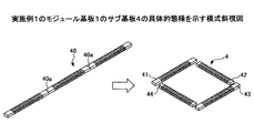
| JP2014165210A (ja) | モジュール基板 | |
| JP2007048976A (ja) | プリント回路板、およびプリント回路板を備えた電子機器 | |
| JP2021158225A (ja) | シールドケース及び電子回路モジュール | |
| TW201605002A (zh) | 半導體封裝 | |
| JP2015135906A (ja) | プリント配線板および情報処理装置 | |
| JP5300994B2 (ja) | 電子機器 | |
| JP2013157565A (ja) | 電子機器 | |
| JP2016082022A (ja) | 回路モジュール | |
| JPWO2020021743A1 (ja) | プリント回路板 | |
| JP5300995B2 (ja) | 電子機器 | |
| JP5908508B2 (ja) | プリント基板 | |
| CN102169877A (zh) | 电路模块、包括电路模块的电子设备及电路模块制造方法 | |
| KR101473478B1 (ko) | 인쇄회로 기판의 모듈 실장 구조 | |
| JP3185456U (ja) | 余剰はんだによる部品の実装不良を抑制するプリント配線板 | |
| JP2012099751A (ja) | プリント回路板 | |
| JP6124258B2 (ja) | 電子回路ユニット及び電子回路ユニットの製造方法 | |
| JP2011103368A (ja) | 実装基板、電子機器および実装基板の製造方法 | |
| JP6378906B2 (ja) | 電子回路モジュール用基板、電子回路モジュール用基板のための多面取り基板、及び電子回路モジュール用基板の製造方法 | |
| JP2005038929A (ja) | 面実装型電子回路モジュール | |
| JP2008098398A (ja) | 回路装置及びその製造方法 | |
| JP4748455B2 (ja) | 電子部品モジュール | |
| JP2016054190A (ja) | 表面実装型パッケージ及び表面実装型パッケージとバイパスコンデンサの配線方法 |
Legal Events
| Date | Code | Title | Description |
|---|---|---|---|
| A521 | Request for written amendment filed |
Free format text: JAPANESE INTERMEDIATE CODE: A523 Effective date: 20160218 |
|
| A621 | Written request for application examination |
Free format text: JAPANESE INTERMEDIATE CODE: A621 Effective date: 20160218 |
|
| A977 | Report on retrieval |
Free format text: JAPANESE INTERMEDIATE CODE: A971007 Effective date: 20161215 |
|
| A131 | Notification of reasons for refusal |
Free format text: JAPANESE INTERMEDIATE CODE: A131 Effective date: 20161220 |
|
| A02 | Decision of refusal |
Free format text: JAPANESE INTERMEDIATE CODE: A02 Effective date: 20170620 |