JP2014123748A - Light-emitting device - Google Patents
Light-emitting device Download PDFInfo
- Publication number
- JP2014123748A JP2014123748A JP2014003953A JP2014003953A JP2014123748A JP 2014123748 A JP2014123748 A JP 2014123748A JP 2014003953 A JP2014003953 A JP 2014003953A JP 2014003953 A JP2014003953 A JP 2014003953A JP 2014123748 A JP2014123748 A JP 2014123748A
- Authority
- JP
- Japan
- Prior art keywords
- layer
- insulating layer
- oxide semiconductor
- oxide
- halogen element
- Prior art date
- Legal status (The legal status is an assumption and is not a legal conclusion. Google has not performed a legal analysis and makes no representation as to the accuracy of the status listed.)
- Granted
Links
Images


Classifications
-
- H—ELECTRICITY
- H10—SEMICONDUCTOR DEVICES; ELECTRIC SOLID-STATE DEVICES NOT OTHERWISE PROVIDED FOR
- H10P—GENERIC PROCESSES OR APPARATUS FOR THE MANUFACTURE OR TREATMENT OF DEVICES COVERED BY CLASS H10
- H10P14/00—Formation of materials, e.g. in the shape of layers or pillars
- H10P14/20—Formation of materials, e.g. in the shape of layers or pillars of semiconductor materials
- H10P14/38—Formation of materials, e.g. in the shape of layers or pillars of semiconductor materials characterised by treatments done after the formation of the materials
-
- H—ELECTRICITY
- H10—SEMICONDUCTOR DEVICES; ELECTRIC SOLID-STATE DEVICES NOT OTHERWISE PROVIDED FOR
- H10D—INORGANIC ELECTRIC SEMICONDUCTOR DEVICES
- H10D30/00—Field-effect transistors [FET]
- H10D30/01—Manufacture or treatment
- H10D30/021—Manufacture or treatment of FETs having insulated gates [IGFET]
- H10D30/031—Manufacture or treatment of FETs having insulated gates [IGFET] of thin-film transistors [TFT]
-
- H—ELECTRICITY
- H10—SEMICONDUCTOR DEVICES; ELECTRIC SOLID-STATE DEVICES NOT OTHERWISE PROVIDED FOR
- H10D—INORGANIC ELECTRIC SEMICONDUCTOR DEVICES
- H10D30/00—Field-effect transistors [FET]
- H10D30/60—Insulated-gate field-effect transistors [IGFET]
- H10D30/67—Thin-film transistors [TFT]
- H10D30/6704—Thin-film transistors [TFT] having supplementary regions or layers in the thin films or in the insulated bulk substrates for controlling properties of the device
-
- H—ELECTRICITY
- H10—SEMICONDUCTOR DEVICES; ELECTRIC SOLID-STATE DEVICES NOT OTHERWISE PROVIDED FOR
- H10D—INORGANIC ELECTRIC SEMICONDUCTOR DEVICES
- H10D30/00—Field-effect transistors [FET]
- H10D30/60—Insulated-gate field-effect transistors [IGFET]
- H10D30/67—Thin-film transistors [TFT]
- H10D30/6729—Thin-film transistors [TFT] characterised by the electrodes
- H10D30/6737—Thin-film transistors [TFT] characterised by the electrodes characterised by the electrode materials
- H10D30/6739—Conductor-insulator-semiconductor electrodes
-
- H—ELECTRICITY
- H10—SEMICONDUCTOR DEVICES; ELECTRIC SOLID-STATE DEVICES NOT OTHERWISE PROVIDED FOR
- H10D—INORGANIC ELECTRIC SEMICONDUCTOR DEVICES
- H10D30/00—Field-effect transistors [FET]
- H10D30/60—Insulated-gate field-effect transistors [IGFET]
- H10D30/67—Thin-film transistors [TFT]
- H10D30/674—Thin-film transistors [TFT] characterised by the active materials
- H10D30/6755—Oxide semiconductors, e.g. zinc oxide, copper aluminium oxide or cadmium stannate
-
- H—ELECTRICITY
- H10—SEMICONDUCTOR DEVICES; ELECTRIC SOLID-STATE DEVICES NOT OTHERWISE PROVIDED FOR
- H10D—INORGANIC ELECTRIC SEMICONDUCTOR DEVICES
- H10D99/00—Subject matter not provided for in other groups of this subclass
-
- H—ELECTRICITY
- H10—SEMICONDUCTOR DEVICES; ELECTRIC SOLID-STATE DEVICES NOT OTHERWISE PROVIDED FOR
- H10P—GENERIC PROCESSES OR APPARATUS FOR THE MANUFACTURE OR TREATMENT OF DEVICES COVERED BY CLASS H10
- H10P14/00—Formation of materials, e.g. in the shape of layers or pillars
- H10P14/20—Formation of materials, e.g. in the shape of layers or pillars of semiconductor materials
- H10P14/34—Deposited materials, e.g. layers
- H10P14/3402—Deposited materials, e.g. layers characterised by the chemical composition
- H10P14/3434—Deposited materials, e.g. layers characterised by the chemical composition being oxide semiconductor materials
-
- H—ELECTRICITY
- H10—SEMICONDUCTOR DEVICES; ELECTRIC SOLID-STATE DEVICES NOT OTHERWISE PROVIDED FOR
- H10P—GENERIC PROCESSES OR APPARATUS FOR THE MANUFACTURE OR TREATMENT OF DEVICES COVERED BY CLASS H10
- H10P14/00—Formation of materials, e.g. in the shape of layers or pillars
- H10P14/60—Formation of materials, e.g. in the shape of layers or pillars of insulating materials
- H10P14/63—Formation of materials, e.g. in the shape of layers or pillars of insulating materials characterised by the formation processes
- H10P14/6326—Deposition processes
- H10P14/6328—Deposition from the gas or vapour phase
- H10P14/6329—Deposition from the gas or vapour phase using physical ablation of a target, e.g. physical vapour deposition or pulsed laser deposition
-
- H—ELECTRICITY
- H10—SEMICONDUCTOR DEVICES; ELECTRIC SOLID-STATE DEVICES NOT OTHERWISE PROVIDED FOR
- H10W—GENERIC PACKAGES, INTERCONNECTIONS, CONNECTORS OR OTHER CONSTRUCTIONAL DETAILS OF DEVICES COVERED BY CLASS H10
- H10W42/00—Arrangements for protection of devices
-
- H—ELECTRICITY
- H10—SEMICONDUCTOR DEVICES; ELECTRIC SOLID-STATE DEVICES NOT OTHERWISE PROVIDED FOR
- H10P—GENERIC PROCESSES OR APPARATUS FOR THE MANUFACTURE OR TREATMENT OF DEVICES COVERED BY CLASS H10
- H10P14/00—Formation of materials, e.g. in the shape of layers or pillars
- H10P14/20—Formation of materials, e.g. in the shape of layers or pillars of semiconductor materials
- H10P14/22—Formation of materials, e.g. in the shape of layers or pillars of semiconductor materials using physical deposition, e.g. vacuum deposition or sputtering
-
- H—ELECTRICITY
- H10—SEMICONDUCTOR DEVICES; ELECTRIC SOLID-STATE DEVICES NOT OTHERWISE PROVIDED FOR
- H10P—GENERIC PROCESSES OR APPARATUS FOR THE MANUFACTURE OR TREATMENT OF DEVICES COVERED BY CLASS H10
- H10P14/00—Formation of materials, e.g. in the shape of layers or pillars
- H10P14/20—Formation of materials, e.g. in the shape of layers or pillars of semiconductor materials
- H10P14/34—Deposited materials, e.g. layers
- H10P14/3402—Deposited materials, e.g. layers characterised by the chemical composition
- H10P14/3424—Deposited materials, e.g. layers characterised by the chemical composition being Group IIB-VIA materials
- H10P14/3426—Oxides
Landscapes
- Thin Film Transistor (AREA)
- Electroluminescent Light Sources (AREA)
- Liquid Crystal (AREA)
- Formation Of Insulating Films (AREA)
- Semiconductor Integrated Circuits (AREA)
- Physical Deposition Of Substances That Are Components Of Semiconductor Devices (AREA)
- Physical Vapour Deposition (AREA)
- Devices For Indicating Variable Information By Combining Individual Elements (AREA)
- Physics & Mathematics (AREA)
- Optics & Photonics (AREA)
Abstract
【課題】安定した電気的特性を有する酸化物半導体を用いた半導体装置を提供することを
目的の一つとする。
【解決手段】フッ素や塩素に代表されるハロゲン元素により、酸化物半導体層に含まれる
水素や水分(水素原子や、H2Oなど水素原子を含む化合物)などの不純物を、酸化物半
導体層より排除し、上記酸化物半導体層中の不純物濃度を低減する。ハロゲン元素は酸化
物半導体層と接して設けられるゲート絶縁層及び/又は絶縁層に含ませて形成することが
でき、またハロゲン元素を含むガス雰囲気下でのプラズマ処理によって酸化物半導体層に
付着させてもよい。
【選択図】図1An object is to provide a semiconductor device using an oxide semiconductor having stable electrical characteristics.
An impurity such as hydrogen or moisture (a hydrogen atom or a compound containing a hydrogen atom such as H 2 O) contained in an oxide semiconductor layer is removed from an oxide semiconductor layer by a halogen element typified by fluorine or chlorine. And eliminating the impurity concentration in the oxide semiconductor layer. The halogen element can be formed to be included in the gate insulating layer and / or the insulating layer provided in contact with the oxide semiconductor layer, and can be attached to the oxide semiconductor layer by plasma treatment in a gas atmosphere containing the halogen element. May be.
[Selection] Figure 1
Description
酸化物半導体を用いる半導体装置及びその作製方法に関する。 The present invention relates to a semiconductor device using an oxide semiconductor and a manufacturing method thereof.
なお、本明細書中において半導体装置とは、半導体特性を利用することで機能しうる装置
全般を指し、電気光学装置、半導体回路および電子機器は全て半導体装置である。
Note that in this specification, a semiconductor device refers to all devices that can function by utilizing semiconductor characteristics, and an electro-optical device, a semiconductor circuit, and an electronic device are all semiconductor devices.
絶縁表面を有する基板上に形成された半導体薄膜を用いて薄膜トランジスタ(TFT)を
構成する技術が注目されている。薄膜トランジスタは液晶テレビに代表されるような表示
装置に用いられている。薄膜トランジスタに適用可能な半導体薄膜としてシリコン系半導
体材料が公知であるが、その他の材料として酸化物半導体が注目されている。
A technique for forming a thin film transistor (TFT) using a semiconductor thin film formed over a substrate having an insulating surface has attracted attention. Thin film transistors are used in display devices typified by liquid crystal televisions. A silicon-based semiconductor material is known as a semiconductor thin film applicable to a thin film transistor, but an oxide semiconductor has attracted attention as another material.
酸化物半導体の材料としては、酸化亜鉛又は酸化亜鉛を成分とするものが知られている。
そして、電子キャリア濃度が1018/cm3未満である非晶質酸化物(酸化物半導体)
なるもので形成された薄膜トランジスタが開示されている(特許文献1乃至3参照。)。
As materials for oxide semiconductors, zinc oxide or a material containing zinc oxide as a component is known.
An amorphous oxide (oxide semiconductor) having an electron carrier concentration of less than 10 18 / cm 3
There is disclosed a thin film transistor formed of the above (see
しかしながら酸化物半導体は薄膜形成工程において化学量論的組成からのずれが生じてし
まう。例えば、酸素の過不足によって酸化物半導体の電気伝導度が変化してしまう。また
、酸化物半導体の薄膜形成中に混入する水素や水分が酸素(O)−水素(H)結合を形成
して電子供与体となり、電気伝導度を変化させる要因となる。さらにO−Hは極性分子な
ので、酸化物半導体によって作製される薄膜トランジスタのような能動デバイスに対して
特性の変動要因となる。
However, the oxide semiconductor is deviated from the stoichiometric composition in the thin film formation process. For example, the electrical conductivity of an oxide semiconductor changes due to excess or deficiency of oxygen. In addition, hydrogen or moisture mixed during the formation of an oxide semiconductor thin film forms an oxygen (O) -hydrogen (H) bond to become an electron donor, which causes a change in electrical conductivity. Furthermore, since O—H is a polar molecule, it becomes a variable factor of characteristics for an active device such as a thin film transistor manufactured using an oxide semiconductor.
このような問題に鑑み本発明の一形態は、安定した電気的特性を有する酸化物半導体を用
いた半導体装置を提供することを目的とする。
In view of such a problem, an object of one embodiment of the present invention is to provide a semiconductor device including an oxide semiconductor having stable electrical characteristics.
酸化物半導体層を用いる薄膜トランジスタの電気的特性変動を抑止するために、酸化物半
導体層及び、該酸化物半導体層と接して形成される絶縁層との界面において、変動要因と
なる水素、水分、水酸基又は水素化物(水素化合物ともいう)などの不純物を排除する。
In order to suppress fluctuations in electrical characteristics of a thin film transistor using an oxide semiconductor layer, hydrogen, moisture, which cause fluctuations, at the interface between the oxide semiconductor layer and an insulating layer formed in contact with the oxide semiconductor layer, Eliminates impurities such as hydroxyl groups or hydrides (also referred to as hydrogen compounds).
フッ素や塩素に代表されるハロゲン元素により、酸化物半導体層に含まれる水素や水分(
水素原子や、H2Oなど水素原子を含む化合物)などの不純物を、酸化物半導体層より排
除し、上記酸化物半導体層中の不純物濃度を低減する。本明細書において、ハロゲン元素
とは周期表において第17族元素(フッ素(F)、塩素(Cl)、臭素(Br)、ヨウ素
(I)など)のことを意味し、代表的には、フッ素、塩素を用いることができ、用いるハ
ロゲン元素は一種でも複数種でもよい。
Hydrogen and moisture contained in the oxide semiconductor layer (such as fluorine and chlorine)
Impurities such as hydrogen atoms and compounds containing hydrogen atoms such as H 2 O are excluded from the oxide semiconductor layer, and the impurity concentration in the oxide semiconductor layer is reduced. In this specification, a halogen element means a group 17 element (fluorine (F), chlorine (Cl), bromine (Br), iodine (I), etc.) in the periodic table. Chlorine can be used, and one or more halogen elements can be used.
ハロゲン元素は酸化物半導体層と接して設けられるゲート絶縁層、保護絶縁層となる絶縁
層に含ませて形成することができ、またハロゲン元素を含むガス雰囲気下でのプラズマ処
理によって酸化物半導体層に付着させてもよい。
The halogen element can be formed by being included in a gate insulating layer provided in contact with the oxide semiconductor layer and an insulating layer serving as a protective insulating layer, and can be formed by plasma treatment in a gas atmosphere containing a halogen element. It may be attached to.
ハロゲン元素は成膜中にゲート絶縁層や絶縁層に含まれるように、成膜ガス(スパッタガ
ス)に導入してもよいし、前工程におけるクリーニング処理によって処理室に残留したハ
ロゲン元素を用いて膜中に含ませてもよい。また、成膜後にゲート絶縁層や絶縁層に添加
してもよい。また、プラズマ処理によって酸化物半導体層との界面に付着させてもよい。
ゲート絶縁層や絶縁層にハロゲン元素を含ませる場合、ゲート絶縁層や絶縁層中における
ハロゲン元素濃度は5×10¹⁸atoms/cm3乃至1×1020atoms/cm
3程度とすればよい。
The halogen element may be introduced into a deposition gas (sputtering gas) so as to be included in the gate insulating layer or the insulating layer during the film formation, or the halogen element remaining in the treatment chamber by the cleaning process in the previous process is used. It may be included in the film. Further, it may be added to the gate insulating layer or the insulating layer after film formation. Alternatively, the oxide semiconductor layer may be attached to the interface with plasma treatment.
When the gate insulating layer or the insulating layer contains a halogen element, the halogen element concentration in the gate insulating layer or the insulating layer is 5 × 10 18 atoms /
What is necessary is just about 3 .
上記いずれかの方法でハロゲン元素により、酸化物半導体層に含まれる水素、水分、水酸
基又は水素化物などの不純物を、ゲート絶縁層、及び/又は絶縁層に拡散させ、上記酸化
物半導体層中の不純物濃度を低減させる。
An impurity such as hydrogen, moisture, a hydroxyl group, or a hydride contained in the oxide semiconductor layer is diffused into the gate insulating layer and / or the insulating layer by the halogen element by any of the above methods, and the oxide semiconductor layer Reduce impurity concentration.
また、絶縁層は酸素過剰とし、不対結合手に代表される欠陥を多く含むことが好ましい。
欠陥を多く含む絶縁層は、主に水素に対して束縛エネルギーがより大きくなり、酸化物半
導体層から絶縁層への拡散がより促進され、絶縁層において不純物が安定化させることが
できるため好ましい。
The insulating layer is preferably oxygen-excess and contains many defects typified by dangling bonds.
An insulating layer containing a large number of defects is preferable because binding energy is mainly larger than that of hydrogen, diffusion from the oxide semiconductor layer to the insulating layer is further promoted, and impurities can be stabilized in the insulating layer.
また、ゲート絶縁層、酸化物半導体層、又は酸化物半導体層に接する絶縁層を、クライオ
ポンプを用いて排気して不純物濃度が低減された成膜室内で、成膜すればよい。
The gate insulating layer, the oxide semiconductor layer, or the insulating layer in contact with the oxide semiconductor layer may be formed in a deposition chamber in which the impurity concentration is reduced by evacuation using a cryopump.
また、ゲート絶縁層、酸化物半導体層、及び酸化物半導体層に接する絶縁層を、成膜する
際に用いるスパッタガス(ハロゲン元素を含むガスも含め)も水素、水、水酸基又は水素
化物などの不純物が、濃度ppm程度、濃度ppb程度まで除去された高純度ガスを用い
ることが好ましい。
A sputtering gas (including a gas containing a halogen element) used for forming the gate insulating layer, the oxide semiconductor layer, and the insulating layer in contact with the oxide semiconductor layer is also hydrogen, water, a hydroxyl group, hydride, or the like. It is preferable to use a high purity gas from which impurities are removed to a concentration of about ppm and a concentration of about ppb.
本明細書で開示する発明の構成の一形態は、ゲート電極層と、ゲート電極層上にハロゲン
元素を含むゲート絶縁層と、ハロゲン元素を含むゲート絶縁層上に酸化物半導体層と、酸
化物半導体層上にソース電極層及びドレイン電極層と、酸化物半導体層、ソース電極層及
びドレイン電極層上に酸化物半導体層の一部と接する絶縁層を有する半導体装置である。
One embodiment of the structure of the invention disclosed in this specification includes a gate electrode layer, a gate insulating layer containing a halogen element over the gate electrode layer, an oxide semiconductor layer over the gate insulating layer containing a halogen element, and an oxide A semiconductor device includes a source electrode layer and a drain electrode layer over a semiconductor layer, and an oxide semiconductor layer, and an insulating layer in contact with part of the oxide semiconductor layer over the source electrode layer and the drain electrode layer.
本明細書で開示する発明の構成の他の一形態は、ゲート電極層と、ゲート電極層上にゲー
ト絶縁層と、ゲート絶縁層上に酸化物半導体層と、酸化物半導体層上にソース電極層及び
ドレイン電極層と、酸化物半導体層、ソース電極層及びドレイン電極層上に酸化物半導体
層の一部と接するハロゲン元素を含む絶縁層を有する半導体装置である。
Another embodiment of the structure of the invention disclosed in this specification includes a gate electrode layer, a gate insulating layer over the gate electrode layer, an oxide semiconductor layer over the gate insulating layer, and a source electrode over the oxide semiconductor layer. The semiconductor device includes a layer and a drain electrode layer, and an insulating layer containing a halogen element in contact with part of the oxide semiconductor layer over the oxide semiconductor layer, the source electrode layer, and the drain electrode layer.
本明細書で開示する発明の構成の他の一形態は、ゲート電極層と、ゲート電極層上にハロ
ゲン元素を含むゲート絶縁層と、ハロゲン元素を含むゲート絶縁層上に酸化物半導体層と
、酸化物半導体層上にソース電極層及びドレイン電極層と、酸化物半導体層、ソース電極
層及びドレイン電極層上に酸化物半導体層の一部と接するハロゲン元素を含む絶縁層を有
する半導体装置である。
Another embodiment of the structure of the invention disclosed in this specification includes a gate electrode layer, a gate insulating layer containing a halogen element over the gate electrode layer, an oxide semiconductor layer over the gate insulating layer containing a halogen element, A semiconductor device includes a source electrode layer and a drain electrode layer over an oxide semiconductor layer, and an insulating layer containing a halogen element in contact with part of the oxide semiconductor layer over the oxide semiconductor layer and the source electrode layer and the drain electrode layer. .
上記構成において、さらに絶縁層を覆う保護絶縁層を有する構成であってもよい。また、
ゲート絶縁層を積層構造とし、ゲート電極層側から窒化物絶縁層、酸化物絶縁層からなる
積層としてもよい。この場合、少なくとも酸化物半導体層と接する酸化物絶縁層にハロゲ
ン元素を含ませるとよい。
In the above structure, a structure having a protective insulating layer covering the insulating layer may be used. Also,
The gate insulating layer may have a stacked structure, and may include a nitride insulating layer and an oxide insulating layer from the gate electrode layer side. In this case, it is preferable that a halogen element be included in at least the oxide insulating layer in contact with the oxide semiconductor layer.
本明細書で開示する発明の構成の他の一形態は、基板上にゲート電極層を形成し、該基板
をハロゲン元素を含むガスを用いてクリーニング処理し減圧状態に保持された第1の処理
室に導入し、ゲート電極層を覆うハロゲン元素を含むゲート絶縁層を形成した後、該基板
を減圧状態に保持された第2の処理室に導入し、第2の処理室内の残留水分を除去しつつ
水素及び水分が除去されたスパッタガスを導入し、第2の処理室内に装着された金属酸化
物のターゲットを用いてハロゲン元素を含むゲート絶縁層上に酸化物半導体層を形成し、
酸化物半導体層上にソース電極層及びドレイン電極層を形成した後、該基板を第3の処理
室に導入し、第3の処理室内の残留水分を除去しつつ水素及び水分が除去された酸素を含
むスパッタガスを導入し、第3の処理室内に装着されたシリコンを含むターゲットを用い
て、酸化物半導体層上に、絶縁層を形成し、該基板を100℃乃至400℃の温度に加熱
して酸化物半導体層中に含まれる水素若しくは水分をハロゲン元素を含むゲート絶縁層側
に拡散させる半導体装置の作製方法である。
Another embodiment of the structure of the invention disclosed in this specification is a first process in which a gate electrode layer is formed over a substrate, the substrate is cleaned using a gas containing a halogen element, and the substrate is kept under reduced pressure. After introducing into the chamber and forming a gate insulating layer containing a halogen element covering the gate electrode layer, the substrate is introduced into the second processing chamber held under reduced pressure to remove residual moisture in the second processing chamber. Then, a sputtering gas from which hydrogen and moisture have been removed is introduced, and an oxide semiconductor layer is formed over the gate insulating layer containing a halogen element using a metal oxide target mounted in the second treatment chamber.
After the source electrode layer and the drain electrode layer are formed over the oxide semiconductor layer, the substrate is introduced into the third treatment chamber, and oxygen from which hydrogen and moisture are removed while moisture remaining in the third treatment chamber is removed. An insulating layer is formed over the oxide semiconductor layer with the use of a target containing silicon mounted in the third treatment chamber, and the substrate is heated to a temperature of 100 ° C. to 400 ° C. Thus, a method for manufacturing a semiconductor device in which hydrogen or moisture contained in an oxide semiconductor layer is diffused to the gate insulating layer side containing a halogen element.
上記構成において、酸化物半導体層中に含まれる水素若しくは水分をハロゲン元素を含む
ゲート絶縁層側に拡散させる加熱処理は、ハロゲン元素を含むゲート絶縁層上に酸化物半
導体層が形成した後であればいつ行ってもよく、絶縁層の形成前に行ってもよい。
In the above structure, heat treatment for diffusing hydrogen or moisture contained in the oxide semiconductor layer to the gate insulating layer containing a halogen element may be performed after the oxide semiconductor layer is formed over the gate insulating layer containing a halogen element. It may be performed at any time or before the formation of the insulating layer.
本明細書で開示する発明の構成の他の一形態は、基板上にゲート電極層及び該ゲート電極
層を覆うゲート絶縁層を形成した後、該基板を減圧状態に保持された第1の処理室に導入
し、第1の処理室内の残留水分を除去しつつ水素及び水分が除去されたスパッタガスを導
入し、第1の処理室内に装着された金属酸化物のターゲットを用いてゲート絶縁層上に酸
化物半導体層を形成し、酸化物半導体層上にソース電極層及びドレイン電極層を形成した
後、該基板を第2の処理室に導入し、第2の処理室内の残留水分を除去しつつ水素及び水
分が除去された酸素及びハロゲン元素を含むスパッタガスを導入し、第2の処理室内に装
着されたシリコンを含むターゲットを用いて、酸化物半導体層上に、ハロゲン元素を含む
絶縁層を形成し、該基板を100℃乃至400℃の温度に加熱して酸化物半導体層中に含
まれる水素若しくは水分をハロゲン元素を含む絶縁層側に拡散させる半導体装置の作製方
法である。
Another embodiment of the structure of the invention disclosed in this specification is a first treatment in which a gate electrode layer and a gate insulating layer covering the gate electrode layer are formed over the substrate, and then the substrate is held under reduced pressure. The gate insulating layer is introduced into the chamber by introducing a sputtering gas from which hydrogen and moisture have been removed while removing residual moisture in the first processing chamber, and using a metal oxide target mounted in the first processing chamber. An oxide semiconductor layer is formed over the source electrode layer and the drain electrode layer over the oxide semiconductor layer, and then the substrate is introduced into the second treatment chamber to remove residual moisture in the second treatment chamber. However, a sputtering gas containing oxygen and a halogen element from which hydrogen and moisture have been removed is introduced, and an insulation containing a halogen element is formed over the oxide semiconductor layer using a target containing silicon mounted in the second treatment chamber. Layer is formed and the substrate is The 0 ℃ to 400 ° C. hydrogen or moisture contained heated in the oxide semiconductor layer to a temperature which is a method for manufacturing a semiconductor device to diffuse the insulating layer side containing a halogen element.
本明細書で開示する発明の構成の他の一形態は、基板上にゲート電極層及び該ゲート電極
層を覆うゲート絶縁層を形成した後、該基板を減圧状態に保持された第1の処理室に導入
し、第1の処理室内の残留水分を除去しつつ水素及び水分が除去されたスパッタガスを導
入し、第1の処理室内に装着された金属酸化物のターゲットを用いてゲート絶縁層上に酸
化物半導体層を形成し、酸化物半導体層上にソース電極層及びドレイン電極層を形成した
後、酸化物半導体層にハロゲン元素を含むガス雰囲気下でプラズマ処理を行い酸化物半導
体層表面にハロゲン元素を付着させ、該基板を第2の処理室に導入し、第2の処理室内の
残留水分を除去しつつ水素及び水分が除去された酸素を含むスパッタガスを導入し、第2
の処理室内に装着されたシリコンを含むターゲットを用いて、酸化物半導体層上に、絶縁
層を形成し、該基板を100℃乃至400℃の温度に加熱して酸化物半導体層中に含まれ
る水素若しくは水分を絶縁層側に拡散させる半導体装置の作製方法である。
Another embodiment of the structure of the invention disclosed in this specification is a first treatment in which a gate electrode layer and a gate insulating layer covering the gate electrode layer are formed over the substrate, and then the substrate is held under reduced pressure. The gate insulating layer is introduced into the chamber by introducing a sputtering gas from which hydrogen and moisture have been removed while removing residual moisture in the first processing chamber, and using a metal oxide target mounted in the first processing chamber. An oxide semiconductor layer is formed over the oxide semiconductor layer, a source electrode layer and a drain electrode layer are formed over the oxide semiconductor layer, and then the oxide semiconductor layer is subjected to plasma treatment in a gas atmosphere containing a halogen element. A halogen element is attached to the substrate, the substrate is introduced into the second treatment chamber, a sputtering gas containing hydrogen and oxygen from which moisture has been removed is introduced while removing residual moisture in the second treatment chamber,
An insulating layer is formed over the oxide semiconductor layer using a silicon-containing target mounted in the treatment chamber, and the substrate is heated to a temperature of 100 ° C. to 400 ° C. to be contained in the oxide semiconductor layer. This is a method for manufacturing a semiconductor device in which hydrogen or moisture is diffused to the insulating layer side.
上記半導体装置の作製方法において、絶縁層を形成する際の基板温度は0℃乃至50℃の
温度とすることができる。
In the above method for manufacturing a semiconductor device, the substrate temperature when forming the insulating layer can be set to 0 ° C. to 50 ° C.
上記半導体装置の作製方法において、ゲート絶縁層、及び/又は酸化物半導体層、及び/
又は絶縁層を作製する際に、第1の処理室及び/又は第2の処理室及び/又は第3の処理
室の排気は吸着型の真空ポンプを用いることが好ましい。例えば、クライオポンプ、イオ
ンポンプ、チタンサブリメーションポンプを用いることが好ましい。上記吸着型の真空ポ
ンプは、ゲート絶縁層、及び/又は酸化物半導体層、及び/又は絶縁層に含まれる水素、
水、水酸基又は水素化物の量を低減するように作用する。
In the above method for manufacturing a semiconductor device, a gate insulating layer and / or an oxide semiconductor layer, and / or
Alternatively, when the insulating layer is formed, an adsorption-type vacuum pump is preferably used for exhausting the first processing chamber and / or the second processing chamber and / or the third processing chamber. For example, it is preferable to use a cryopump, an ion pump, or a titanium sublimation pump. The adsorption-type vacuum pump includes a gate insulating layer and / or an oxide semiconductor layer, and / or hydrogen contained in the insulating layer,
It acts to reduce the amount of water, hydroxyl groups or hydrides.
上記半導体装置の作製方法において、酸化物半導体層を成膜するためのターゲットは、酸
化亜鉛を主成分として含むものを用いることができる。また、ターゲットとして、インジ
ウム、ガリウム、亜鉛を含む金属酸化物を用いることができる。
In the above method for manufacturing a semiconductor device, a target for forming an oxide semiconductor layer can be a target containing zinc oxide as a main component. As the target, a metal oxide containing indium, gallium, and zinc can be used.
上記半導体装置の作製方法において、絶縁層として酸化シリコン層を成膜するためのシリ
コンを含むターゲットは、シリコン半導体のターゲット又は合成石英のターゲットを用い
ることができる。
In the above method for manufacturing a semiconductor device, a silicon semiconductor target or a synthetic quartz target can be used as a target containing silicon for forming a silicon oxide layer as an insulating layer.
上記各構成は、上記課題の少なくとも一つを解決する。 Each of the above configurations solves at least one of the above problems.
なお、酸化物半導体層としては、InMO3(ZnO)m(m>0)で表記される薄膜で
あり、その薄膜を酸化物半導体層として用いた薄膜トランジスタを作製する。なお、Mは
、Ga、Fe、Ni、Mn及びCoから選ばれた一の金属元素または複数の金属元素を示
す。例えばMとして、Gaの場合があることの他、GaとNiまたはGaとFeなど、G
a以外の上記金属元素が含まれる場合がある。また、上記酸化物半導体において、Mとし
て含まれる金属元素の他に、不純物元素としてFe、Niその他の遷移金属元素、または
該遷移金属の酸化物が含まれているものがある。本明細書においては、InMO3(Zn
O)m(m>0)で表記される構造の酸化物半導体層のうち、MとしてGaを含む構造の
酸化物半導体をIn−Ga−Zn−O系酸化物半導体とよび、その薄膜をIn−Ga−Z
n−O系非単結晶膜とも呼ぶ。
Note that the oxide semiconductor layer is a thin film represented by InMO 3 (ZnO) m (m> 0), and a thin film transistor using the thin film as an oxide semiconductor layer is manufactured. Note that M represents one metal element or a plurality of metal elements selected from Ga, Fe, Ni, Mn, and Co. For example, as M, there may be a case of Ga, Ga and Ni or Ga and Fe, etc.
The metal element other than a may be contained. In addition to the metal element contained as M, some of the above oxide semiconductors contain Fe, Ni, other transition metal elements, or oxides of the transition metal as impurity elements. In this specification, InMO 3 (Zn
Among oxide semiconductor layers having a structure represented by O) m (m> 0), an oxide semiconductor having a structure containing Ga as M is referred to as an In—Ga—Zn—O-based oxide semiconductor, and a thin film thereof is referred to as In. -Ga-Z
Also called an n-O non-single crystal film.
また、酸化物半導体層に適用する金属酸化物として上記の他にも、In−Sn−O系、I
n−Sn−Zn−O系、In−Al−Zn−O系、Sn−Ga−Zn−O系、Al−Ga
−Zn−O系、Sn−Al−Zn−O系、In−Zn−O系、Sn−Zn−O系、Al−
Zn−O系、In−O系、Sn−O系、Zn−O系の金属酸化物を適用することができる
。また上記金属酸化物からなる酸化物半導体層に酸化シリコンを含ませてもよい。
In addition to the above, as a metal oxide used for the oxide semiconductor layer, an In—Sn—O-based material, I
n-Sn-Zn-O, In-Al-Zn-O, Sn-Ga-Zn-O, Al-Ga
-Zn-O, Sn-Al-Zn-O, In-Zn-O, Sn-Zn-O, Al-
A Zn—O-based, In—O-based, Sn—O-based, or Zn—O-based metal oxide can be used. Further, silicon oxide may be included in the oxide semiconductor layer formed of the metal oxide.
また、酸化物半導体層とソース電極及びドレイン電極の間に、酸化物導電層を形成しても
よい。酸化物導電層とソース電極及びドレイン電極を形成するための金属層は、連続成膜
が可能である。
Further, an oxide conductive layer may be formed between the oxide semiconductor layer and the source and drain electrodes. The metal layer for forming the oxide conductive layer and the source and drain electrodes can be continuously formed.
また、薄膜トランジスタは静電気などにより破壊されやすいため、ゲート線またはソース
線に対して、画素部の薄膜トランジスタの保護用の保護回路を同一基板上に設けることが
好ましい。保護回路は、酸化物半導体層を用いた非線形素子を用いて構成することが好ま
しい。
In addition, since the thin film transistor is easily broken by static electricity or the like, it is preferable to provide a protective circuit for protecting the thin film transistor in the pixel portion over the same substrate with respect to the gate line or the source line. The protective circuit is preferably formed using a non-linear element using an oxide semiconductor layer.
なお、第1、第2として付される序数詞は便宜上用いるものであり、工程順又は積層順を
示すものではない。また、本明細書において発明を特定するための事項として固有の名称
を示すものではない。
In addition, the ordinal numbers attached as the first and second are used for convenience and do not indicate the order of steps or the order of lamination. In addition, a specific name is not shown as a matter for specifying the invention in this specification.
安定した電気的特性を有する酸化物半導体を用いた半導体装置を提供することができる。 A semiconductor device including an oxide semiconductor having stable electrical characteristics can be provided.
以下では、本発明の実施の形態について図面を用いて詳細に説明する。ただし、本発明は
以下の説明に限定されず、その形態および詳細を様々に変更し得ることは、当業者であれ
ば容易に理解される。また、本発明は以下に示す実施の形態の記載内容に限定して解釈さ
れるものではない。
Hereinafter, embodiments of the present invention will be described in detail with reference to the drawings. However, the present invention is not limited to the following description, and it will be easily understood by those skilled in the art that modes and details can be variously changed. In addition, the present invention is not construed as being limited to the description of the embodiments below.
(実施の形態1)
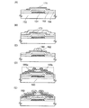
本実施の形態の半導体装置及び半導体装置の作製方法の一形態を、図1を用いて説明する
。本実施の形態で示す半導体装置は薄膜トランジスタである。
(Embodiment 1)
One embodiment of a semiconductor device and a method for manufacturing the semiconductor device of this embodiment will be described with reference to FIGS. The semiconductor device described in this embodiment is a thin film transistor.
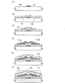
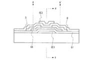
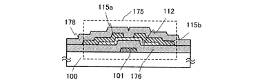
図1(A)乃至(F)に半導体装置の断面構造の一例を示す。図1(A)乃至(F)に示
す薄膜トランジスタ110は、ボトムゲート構造の一つであり逆スタガ型薄膜トランジス
タともいう。
1A to 1F illustrate an example of a cross-sectional structure of a semiconductor device. A
図1(A)乃至(F)に示す薄膜トランジスタ110は、絶縁表面を有する基板100上
に、ゲート電極層101、ゲート絶縁層131、ゲート絶縁層132、酸化物半導体層1
12、ソース電極層115a、及びドレイン電極層115bを含む。また、薄膜トランジ
スタ110を覆い、酸化物半導体層112に接する酸化物絶縁層116が設けられ、さら
にその上に保護絶縁層103が積層されている。
1A to 1F includes a
12, a
酸化物半導体層を用いる薄膜トランジスタの電気的特性変動を抑止するために、酸化物半
導体層及び、該酸化物半導体層と接して形成されるゲート絶縁層及び/又は絶縁層との界
面において、変動要因となる水素、水分、水酸基又は水素化物(水素化合物ともいう)な
どの不純物を排除する。具体的には、酸化物半導体層及び、該酸化物半導体層と接して形
成される絶縁層との界面における水素濃度は5×10¹⁹atoms/cm3以下、好ま
しくは1×10¹⁹atoms/cm3以下とすることが望ましい。
In order to suppress variation in electrical characteristics of a thin film transistor using an oxide semiconductor layer, a variation factor is generated at the interface between the oxide semiconductor layer and the gate insulating layer and / or the insulating layer formed in contact with the oxide semiconductor layer. Impurities such as hydrogen, moisture, hydroxyl groups or hydrides (also referred to as hydrogen compounds) are eliminated. Specifically, the hydrogen concentration at the interface between the oxide semiconductor layer and the insulating layer formed in contact with the oxide semiconductor layer is 5 × 10 19 atoms / cm 3 or less, preferably 1 × 10 19 atoms / cm 3. 3 or less is desirable.
フッ素や塩素に代表されるハロゲン元素により、酸化物半導体層に含まれる水素や水分(
水素原子や、H2Oなど水素原子を含む化合物)などの不純物を、酸化物半導体層より排
除し、上記酸化物半導体層中の不純物濃度を低減する。ゲート絶縁層や絶縁層にハロゲン
元素を含ませる場合、ゲート絶縁層や絶縁層中におけるハロゲン元素濃度は5×10¹⁸
atoms/cm3乃至1×1020atoms/cm3程度とすればよい。
Hydrogen and moisture contained in the oxide semiconductor layer (such as fluorine and chlorine)
Impurities such as hydrogen atoms and compounds containing hydrogen atoms such as H 2 O are excluded from the oxide semiconductor layer, and the impurity concentration in the oxide semiconductor layer is reduced. When the gate insulating layer or the insulating layer contains a halogen element, the halogen element concentration in the gate insulating layer or the insulating layer is 5 × 10 18.
Atoms /
なお、前記水素濃度及びハロゲン元素濃度は二次イオン質量分析(SIMS:Secon
dary Ion Mass Spectrometry)による各濃度の定量結果であ
る。
The hydrogen concentration and the halogen element concentration are measured by secondary ion mass spectrometry (SIMS: Secon).
It is a quantification result of each density | concentration by (dary Ion Mass Spectrometry).
ハロゲン元素は酸化物半導体層と接して設けられるゲート絶縁層、絶縁層に含ませて形成
することができ、またハロゲン元素を含むガス雰囲気下でのプラズマ処理によって酸化物
半導体層に付着させてもよい。上記ハロゲン元素を半導体装置に含ませる方法(成膜時に
ゲート絶縁層に含ませる、成膜時に絶縁層に含ませる、プラズマ処理により絶縁層との界
面に付着させる)は、少なくとも1つ以上行えばよく、もちろん複数行ってもよい。
The halogen element can be formed so as to be included in the gate insulating layer and the insulating layer provided in contact with the oxide semiconductor layer, or may be attached to the oxide semiconductor layer by plasma treatment in a gas atmosphere containing the halogen element. Good. At least one or more methods for including the halogen element in the semiconductor device (including in the gate insulating layer during film formation, included in the insulating layer during film formation, and attached to the interface with the insulating layer by plasma treatment) may be performed. Of course, you can go multiple times.
上記少なくともいずれかの方法でハロゲン元素により、酸化物半導体層に含まれる水素、
水分、水酸基又は水素化物などの不純物を、ゲート絶縁層、及び/又は絶縁層に拡散させ
、上記酸化物半導体層中の不純物濃度を低減させる。
Hydrogen contained in the oxide semiconductor layer by a halogen element by at least one of the above methods,
Impurities such as moisture, hydroxyl, or hydride are diffused into the gate insulating layer and / or the insulating layer, so that the impurity concentration in the oxide semiconductor layer is reduced.
ハロゲン元素が水素などの不純物に与える影響を結合エネルギーの計算により検証した。
ハロゲン元素としてはフッ素(F)、ハロゲン元素が含まれる絶縁層としては酸化シリコ
ン(SiOx)を用いた。
The effect of halogen elements on impurities such as hydrogen was verified by calculating the binding energy.
Fluorine (F) was used as the halogen element, and silicon oxide (SiO x ) was used as the insulating layer containing the halogen element.
なお、計算には、Gauss基底を用いた密度汎関数法(DFT)を用いた。DFTでは
、交換相関相互作用を電子密度で表現された一電子ポテンシャルの汎関数(関数の関数の
意)で近似しているため、計算は高速かつ高精度である。ここでは、混合汎関数であるB
3LYPを用いて、交換と相関エネルギーに係る各パラメータの重みを規定した。また、
基底関数として、6−311G(それぞれの原子価軌道に三つの短縮関数を用いたtri
ple split valence基底系の基底関数)を全ての原子に適用した。上述
の基底関数により、例えば、水素原子であれば、1s〜3sの軌道が考慮され、また、酸
素原子であれば、1s〜4s、2p〜4pの軌道が考慮されることになる。さらに、計算
精度向上のため、分極基底系として、水素原子にはp関数を、水素原子以外にはd関数を
加えた。なお、量子化学計算プログラムとしては、Gaussian 03を使用した。
計算は、ハイパフォーマンスコンピュータ(SGI社製、Altix4700)を用いて
行った。
For the calculation, a density functional method (DFT) using a Gauss basis was used. In DFT, the exchange correlation interaction is approximated by a functional (meaning function function) of a one-electron potential expressed in electron density, so that the calculation is fast and accurate. Here, B is a mixed functional
3LYP was used to define the weight of each parameter related to exchange and correlation energy. Also,
As a basis function, 6-311G (tri using three shortening functions for each valence orbital)
ple split valence basis set) was applied to all atoms. With the above-mentioned basis functions, for example, orbits of 1s to 3s are considered for hydrogen atoms, and orbits of 1s to 4s and 2p to 4p are considered for oxygen atoms. Furthermore, in order to improve calculation accuracy, a p function was added to hydrogen atoms and a d function was added to other than hydrogen atoms as a polarization basis set. Note that Gaussian 03 was used as the quantum chemistry calculation program.
The calculation was performed using a high performance computer (manufactured by SGI, Altix 4700).
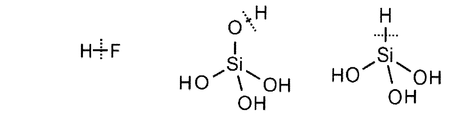
以下では、フッ素が点在した酸化シリコン(SiO2)中に、水素がマイグレーションし
た場合に、水素がフッ素に結合するか、SiO2中の酸素に結合するか、SiO2中のシ
リコンに結合するかについて計算を行った。具体的には、フッ素を添加したSiO2中に
水素が存在するとき、水素がフッ素、酸素とシリコンのどの原子と結合を形成すると安定
化するかを計算した。図30に計算モデルの模式図を示す。また、表1にH−F、H−O
、H−Si結合の結合エネルギーを示す。
In the following, in the silicon oxide with fluorine interspersed (SiO 2), when the hydrogen has migrated, whether hydrogen is bonded to a fluorine, or bonded to the oxygen in SiO 2, is bonded to the silicon in SiO 2 Calculations were made. Specifically, when hydrogen is present in SiO 2 to which fluorine has been added, it was calculated which atom of which fluorine, oxygen and silicon would form a bond when hydrogen was bonded. FIG. 30 shows a schematic diagram of a calculation model. Table 1 shows HF, HO.
, Shows the bond energy of the H-Si bond.

表1に示すように、水素は酸素やシリコンと結合するよりも、フッ素と結合しやすい事が
わかる。よって、フッ素が添加されたSiOxを層間膜に用いる事で、加熱処理によりマ
イグレーションしている水素はSiOx中のフッ素と結合して安定化し、捉えられやすい
と言える。
As shown in Table 1, it can be seen that hydrogen is more likely to bind to fluorine than to oxygen or silicon. Therefore, it can be said that by using SiO x to which fluorine is added for the interlayer film, hydrogen migrated by the heat treatment is combined with fluorine in SiO x to be stabilized and easily captured.
フッ素や塩素に代表されるハロゲン元素は電気陰性度が大きいために、不純物である水素
の電気陰性度との差が大きく、ハロゲン元素と水素とはイオン結合の結合力が大きく作用
する。
Since halogen elements typified by fluorine and chlorine have a large electronegativity, there is a large difference from the electronegativity of hydrogen, which is an impurity, and the binding force of ionic bonds acts greatly between halogen elements and hydrogen.
従って、ゲート絶縁層又は/及び絶縁層に含まれるハロゲン元素により、酸化物半導体層
中の水素や水分(水素原子や、H2Oなど水素原子を含む化合物)などの不純物をゲート
絶縁層又は/及び絶縁層へより効果的に拡散し、酸化物半導体層中より排除することがで
きる。
Therefore, an impurity such as hydrogen or moisture (a hydrogen atom or a compound containing a hydrogen atom such as H 2 O) in the oxide semiconductor layer is removed from the gate insulating layer or / and the halogen element contained in the gate insulating layer or / and the insulating layer. And more effectively diffused into the insulating layer and eliminated from the oxide semiconductor layer.
本実施の形態では、ゲート絶縁層にハロゲン元素を含ませる例であり、酸化物半導体層1
12に接して設けられるゲート絶縁層132はハロゲン元素を含む。
In this embodiment, the gate insulating layer is an example in which a halogen element is included, and the
The
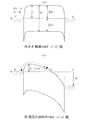
図25は、酸化物半導体を用いた逆スタガ型の薄膜トランジスタの縦断面図を示す。ゲー
ト電極(GE1)上にゲート絶縁膜(GI)を介して酸化物半導体層(OS)が設けられ
、その上にソース電極(S)及びドレイン電極(D)が設けられている。
FIG. 25 is a longitudinal sectional view of an inverted staggered thin film transistor using an oxide semiconductor. An oxide semiconductor layer (OS) is provided over the gate electrode (GE1) through a gate insulating film (GI), and a source electrode (S) and a drain electrode (D) are provided thereover.
図26は、図25に示すA−A’断面におけるエネルギーバンド図(模式図)を示す。図
26(A)はソースとドレインの間の電圧を等電位(VD=0V)とした場合を示し、図
26(B)はソースに対しドレインに正の電位(VD>0)を加えた場合を示す。
26 shows an energy band diagram (schematic diagram) in the section AA ′ shown in FIG. FIG. 26A shows the case where the voltage between the source and the drain is equipotential (VD = 0V), and FIG. 26B shows the case where a positive potential (VD> 0) is applied to the drain with respect to the source. Indicates.
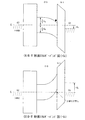
図27は、図25におけるB−B’の断面におけるエネルギーバンド図(模式図)である
。図27(A)はゲート(G1)に正の電位(+VG)が印加された状態であり、ソース
とドレインと間にキャリア(電子)が流れるオン状態を示している。また、図27(B)
は、ゲート(G1)に負の電位(−VG)が印加された状態であり、オフ状態(少数キャ
リアは流れない)である場合を示す。
FIG. 27 is an energy band diagram (schematic diagram) in the section taken along line BB ′ in FIG. FIG. 27A shows a state where a positive potential (+ VG) is applied to the gate (G1), and shows an on state in which carriers (electrons) flow between the source and the drain. In addition, FIG.
Indicates a state in which a negative potential (−VG) is applied to the gate (G1) and an off state (minority carriers do not flow).
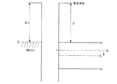
図28は、真空準位と金属の仕事関数(φM)、酸化物半導体の電子親和力(χ)の関係
を示す。
FIG. 28 shows the relationship between the vacuum level, the metal work function (φM), and the electron affinity (χ) of the oxide semiconductor.
常温において金属中の電子は縮退しており、フェルミ準位は伝導帯内に位置する。一方、
従来の酸化物半導体は一般にn型であり、その場合のフェルミ準位(EF)は、バンドギ
ャップ中央に位置する真性フェルミ準位(Ei)から離れて、伝導帯寄りに位置している
。なお、酸化物半導体において水素はドナーでありn型化する一つの要因であることが知
られている。
At room temperature, the electrons in the metal are degenerated and the Fermi level is located in the conduction band. on the other hand,
Conventional oxide semiconductors are generally n-type, and the Fermi level (E F ) in that case is away from the intrinsic Fermi level (Ei) located at the center of the band gap and closer to the conduction band. Note that in an oxide semiconductor, hydrogen is a donor and is known to be one factor of becoming n-type.
これに対して本発明に係る酸化物半導体は、n型不純物である水素を酸化物半導体から除
去し、酸化物半導体の主成分以外の不純物が極力含まれないように高純度化することによ
り真性(i型)とし、又は真性型とせんとしたものである。すなわち、不純物を添加して
i型化するのでなく、水素や水等の不純物を極力除去したことにより、高純度化されたi
型(真性半導体)又はそれに近づけることを特徴としている。そうすることにより、フェ
ルミ準位(EF)は真性フェルミ準位(Ei)と同じレベルにまですることができる。
On the other hand, the oxide semiconductor according to the present invention is intrinsic by removing hydrogen, which is an n-type impurity, from the oxide semiconductor and purifying it so that impurities other than the main component of the oxide semiconductor are contained as much as possible. (I-type) or intrinsic type. In other words, i-type purified by removing impurities such as hydrogen and water as much as possible without adding impurities to make i-type.
It is characterized by its type (intrinsic semiconductor) or its proximity. By doing so, the Fermi level (E F ) can be brought to the same level as the intrinsic Fermi level (Ei).
酸化物半導体のバンドギャップ(Eg)が3.15eVである場合、電子親和力(χ)は
4.3eVと言われている。ソース電極及びドレイン電極を構成するチタン(Ti)の仕
事関数は、酸化物半導体の電子親和力(χ)とほぼ等しい。この場合、金属−酸化物半導
体界面において、電子に対してショットキー型の障壁は形成されない。
When the band gap (Eg) of an oxide semiconductor is 3.15 eV, the electron affinity (χ) is said to be 4.3 eV. The work function of titanium (Ti) constituting the source electrode and the drain electrode is substantially equal to the electron affinity (χ) of the oxide semiconductor. In this case, no Schottky barrier is formed for electrons at the metal-oxide semiconductor interface.
すなわち、金属の仕事関数(φM)と酸化物半導体の電子親和力(χ)がほぼ等しい場合
、両者が接触すると図26(A)で示すようなエネルギーバンド図(模式図)が示される
。
That is, when the work function (φM) of the metal and the electron affinity (χ) of the oxide semiconductor are approximately equal, an energy band diagram (schematic diagram) as shown in FIG.
図26(B)において黒丸(●)は電子を示し、ドレインに正の電位が印加されると、電
子はバリア(h)をこえて酸化物半導体に注入され、ドレインに向かって流れる。この場
合、バリア(h)の高さは、ゲート電圧とドレイン電圧に依存して変化するが、正のドレ
イン電圧が印加された場合には、電圧印加のない図26(A)のバリアの高さすなわちバ
ンドギャップ(Eg)の1/2よりもバリア(h)の高さは小さい値となる。
In FIG. 26B, black circles (●) indicate electrons, and when a positive potential is applied to the drain, the electrons are injected into the oxide semiconductor over the barrier (h) and flow toward the drain. In this case, the height of the barrier (h) changes depending on the gate voltage and the drain voltage. However, when a positive drain voltage is applied, the height of the barrier in FIG. That is, the height of the barrier (h) is smaller than ½ of the band gap (Eg).
このとき電子は、図27(A)で示すようにゲート絶縁膜と高純度化された酸化物半導体
との界面における、酸化物半導体側のエネルギー的に安定な最低部を移動する。
At this time, as shown in FIG. 27A, electrons move through the lowest part of the oxide semiconductor side, which is stable in terms of energy, at the interface between the gate insulating film and the highly purified oxide semiconductor.
また、図27(B)において、ゲート電極(G1)に負の電位(逆バイアス)が印加され
ると、少数キャリアであるホールは実質的にゼロであるため、電流は限りなくゼロに近い
値となる。
In FIG. 27B, when a negative potential (reverse bias) is applied to the gate electrode (G1), the number of holes that are minority carriers is substantially zero; It becomes.
例えば、薄膜トランジスタのチャネル幅Wが1×104μmでチャネル長が3μmの素子
であっても、オフ電流が10−13A以下であり、サブスレッショルドスイング値(S値
)が0.1V/dec.(ゲート絶縁膜厚100nm)が得られる。
For example, even if the thin film transistor has a channel width W of 1 × 10 4 μm and a channel length of 3 μm, the off-current is 10 −13 A or less, and the subthreshold swing value (S value) is 0.1 V / dec. . (Gate insulating
このように、酸化物半導体の主成分以外の不純物が極力含まれないように高純度化するこ
とにより、薄膜トランジスタの動作を良好なものとすることができる。
In this manner, the operation of the thin film transistor can be improved by purification so that impurities other than the main component of the oxide semiconductor are included as much as possible.
また、薄膜トランジスタ110はシングルゲート構造の薄膜トランジスタを用いて説明す
るが、必要に応じて、チャネル形成領域を複数有するマルチゲート構造の薄膜トランジス
タも形成することができる。
Although the
以下、図1(A)乃至(F)を用い、基板100上に薄膜トランジスタ110を作製する
工程を説明する。
Hereinafter, a process for manufacturing the
まず、絶縁表面を有する基板100上に導電膜を形成した後、第1のフォトリソグラフィ
工程及びエッチング工程によりゲート電極層101を形成する(図1(A)参照。)。形
成されたゲート電極層の端部はテーパ形状であると、上に積層するゲート絶縁層の被覆性
が向上するため好ましい。なお、レジストマスクをインクジェット法で形成してもよい。
レジストマスクをインクジェット法で形成するとフォトマスクを使用しないため、製造コ
ストを低減できる。
First, after a conductive film is formed over the
When the resist mask is formed by an ink-jet method, a manufacturing cost can be reduced because a photomask is not used.
絶縁表面を有する基板100に使用することができる基板に大きな制限はないが、少なく
とも、後の加熱処理に耐えうる程度の耐熱性を有していることが必要となる。バリウムホ
ウケイ酸ガラスやアルミノホウケイ酸ガラスなどのガラス基板を用いることができる。
There is no particular limitation on a substrate that can be used as the
また、ガラス基板としては、後の加熱処理の温度が高い場合には、歪み点が730℃以上
のものを用いると良い。また、ガラス基板には、例えば、アルミノシリケートガラス、ア
ルミノホウケイ酸ガラス、バリウムホウケイ酸ガラスなどのガラス材料が用いられている
。なお、酸化ホウ酸と比較して酸化バリウム(BaO)を多く含ませることで、より実用
的な耐熱ガラスが得られる。このため、B2O3よりBaOを多く含むガラス基板を用い
ることが好ましい。
As the glass substrate, a glass substrate having a strain point of 730 ° C. or higher is preferably used when the temperature of the subsequent heat treatment is high. For the glass substrate, for example, a glass material such as aluminosilicate glass, aluminoborosilicate glass, or barium borosilicate glass is used. In addition, a more practical heat-resistant glass can be obtained by containing more barium oxide (BaO) than boric oxide. For this reason, it is preferable to use a glass substrate containing more BaO than B 2 O 3 .
なお、上記のガラス基板に代えて、セラミック基板、石英基板、サファイア基板などの絶
縁体でなる基板を用いても良い。他にも、結晶化ガラスなどを用いることができる。また
、プラスチック基板等も適宜用いることができる。
Note that a substrate formed of an insulator such as a ceramic substrate, a quartz substrate, or a sapphire substrate may be used instead of the glass substrate. In addition, crystallized glass or the like can be used. A plastic substrate or the like can also be used as appropriate.
下地膜となる絶縁膜を基板100とゲート電極層101との間に設けてもよい。下地膜は
、基板100からの不純物元素の拡散を防止する機能があり、窒化シリコン膜、酸化シリ
コン膜、窒化酸化シリコン膜、又は酸化窒化シリコン膜から選ばれた一又は複数の膜によ
る積層構造により形成することができる。
An insulating film serving as a base film may be provided between the
また、ゲート電極層101の材料は、モリブデン、チタン、クロム、タンタル、タングス
テン、アルミニウム、銅、ネオジム、スカンジウム等の金属材料又はこれらを主成分とす
る合金材料を用いて、単層で又は積層して形成することができる。
The material of the
例えば、ゲート電極層101の2層の積層構造としては、アルミニウム層上にモリブデン
層が積層された2層の積層構造、または銅層上にモリブデン層を積層した2層構造、また
は銅層上に窒化チタン層若しくは窒化タンタル層を積層した2層構造、窒化チタン層とモ
リブデン層とを積層した2層構造とすることが好ましい。3層の積層構造としては、タン
グステン層または窒化タングステン層と、アルミニウムとシリコンの合金層またはアルミ
ニウムとチタンの合金層と、窒化チタン層またはチタン層とを積層した積層や、モリブデ
ン層、アルミニウム層、モリブデン層の3層を用いることができる。なお、透光性を有す
る導電膜を用いてゲート電極層を形成することもできる。透光性を有する導電膜としては
、透光性導電性酸化物等をその例に挙げることができる。
For example, the two-layer structure of the
次いで、ゲート電極層101上にゲート絶縁層を形成する。本実施の形態では、ゲート絶
縁層にハロゲン元素を含ませて形成する。ゲート絶縁層が積層構造の場合、少なくとも酸
化物半導体層に接するゲート絶縁層にハロゲン元素を含ませる。
Next, a gate insulating layer is formed over the
ゲート絶縁層は、プラズマCVD法又はスパッタリング法等を用いて、酸化シリコン層、
窒化シリコン層、酸化窒化シリコン層、窒化酸化シリコン層、又は酸化アルミニウム層を
単層で又は積層して形成することができる。スパッタリング法により酸化シリコン層を成
膜する場合には、ターゲットとしてシリコンターゲット又は石英ターゲットを用い、スパ
ッタガスとして酸素又は、酸素及びアルゴンの混合ガスを用いて行う。
The gate insulating layer is formed using a silicon oxide layer, a plasma CVD method, a sputtering method, or the like.
A silicon nitride layer, a silicon oxynitride layer, a silicon nitride oxide layer, or an aluminum oxide layer can be formed as a single layer or a stacked layer. In the case of forming a silicon oxide layer by a sputtering method, a silicon target or a quartz target is used as a target, and oxygen or a mixed gas of oxygen and argon is used as a sputtering gas.
ここで、不純物を除去することによりi型化又は実質的にi型化された酸化物半導体(高
純度化された酸化物半導体)は界面準位、界面電荷に対して極めて敏感であるため、ゲー
ト絶縁層との界面は重要である。そのため高純度化された酸化物半導体に接するゲート絶
縁層(GI)は、高品質化が要求される。
Here, by removing impurities, an i-type or substantially i-type oxide semiconductor (a highly purified oxide semiconductor) is extremely sensitive to interface states and interface charges. The interface with the gate insulating layer is important. Therefore, the gate insulating layer (GI) in contact with the highly purified oxide semiconductor is required to have high quality.
例えば、μ波(2.45GHz)を用いた高密度プラズマCVDは、緻密で絶縁耐圧の高
い高品質な絶縁層を形成できるので好ましい。高純度化された酸化物半導体と高品質ゲー
ト絶縁層とが密接することにより、界面準位を低減して界面特性を良好なものとすること
ができるからである。
For example, high-density plasma CVD using μ-wave (2.45 GHz) is preferable because a high-quality insulating layer with high density and high withstand voltage can be formed. This is because when the highly purified oxide semiconductor and the high-quality gate insulating layer are in close contact with each other, the interface state can be reduced and interface characteristics can be improved.
もちろん、ゲート絶縁層として良質な絶縁層を形成できるものであれば、スパッタリング
法やプラズマCVD法など他の成膜方法を適用することができる。また、成膜後の熱処理
によってゲート絶縁層の膜質、酸化物半導体との界面特性が改質される絶縁層であっても
良い。いずれにしても、ゲート絶縁層としての膜質が良好であることは勿論のこと、酸化
物半導体との界面準位密度を低減し、良好な界面を形成できるものであれば良い。
Needless to say, another film formation method such as a sputtering method or a plasma CVD method can be used as long as a high-quality insulating layer can be formed as the gate insulating layer. Alternatively, an insulating layer in which the film quality of the gate insulating layer and the interface characteristics with the oxide semiconductor are modified by heat treatment after film formation may be used. In any case, any film can be used as long as it can reduce the interface state density with an oxide semiconductor and form a favorable interface as well as the film quality as a gate insulating layer is good.
さらに、85℃、2×10⁶V/cm、12時間のゲートバイアス・熱ストレス試験(B
T試験)においては、不純物が酸化物半導体に添加されていると、不純物と酸化物半導体
の主成分との結合手が、強電界(B:バイアス)と高温(T:温度)により切断され、生
成された不対結合手がしきい値電圧(Vth)のドリフトを誘発することとなる。
Furthermore, a gate bias / thermal stress test (B for 12 hours at 85 ° C., 2 × 10 6 V / cm
In the T test), when an impurity is added to the oxide semiconductor, a bond between the impurity and the main component of the oxide semiconductor is cut by a strong electric field (B: bias) and a high temperature (T: temperature), The generated dangling bond induces a threshold voltage (Vth) drift.
これに対して、本明細書に開示する発明は、酸化物半導体の不純物、特に水素や水等を極
力除去し、上記のようにゲート絶縁層との界面特性を良好にすることにより、BT試験に
対しても安定な薄膜トランジスタを得ることを可能としている。
In contrast, the invention disclosed in this specification removes impurities of oxide semiconductors, particularly hydrogen and water, as much as possible, and improves the interface characteristics with the gate insulating layer as described above, thereby performing the BT test. It is possible to obtain a stable thin film transistor.
本実施の形態では、ゲート電極層101側からゲート絶縁層131、ゲート絶縁層132
の積層構造でゲート絶縁層を形成する(図1(B)参照。)。積層するゲート絶縁層は、
ゲート電極層101側から窒化シリコン層と酸化シリコン層の積層構造を用いることがで
きる。ゲート絶縁層131としてスパッタリング法により膜厚50nm以上200nm以
下の窒化シリコン層(SiNy(y>0))を形成し、ゲート絶縁層131上にゲート絶
縁層132として膜厚5nm以上300nm以下のハロゲン元素を含む酸化シリコン層(
SiOx(x>0))を積層して、膜厚100nmのゲート絶縁層とする。
In this embodiment, the
A gate insulating layer is formed with the stacked structure (see FIG. 1B). The gate insulating layer to be stacked is
A stacked structure of a silicon nitride layer and a silicon oxide layer can be used from the
SiO x (x> 0)) is stacked to form a gate insulating layer having a thickness of 100 nm.
ハロゲン元素は成膜中にゲート絶縁層に含まれるように、成膜ガス(スパッタガス)に導
入してもよいし、前工程におけるクリーニング処理によって処理室に残留したハロゲン元
素を用いて膜中に含ませてもよい。また、成膜後にゲート絶縁層に添加してもよい。
The halogen element may be introduced into a deposition gas (sputtering gas) so as to be included in the gate insulating layer during the film formation, or the halogen element remaining in the processing chamber by the cleaning process in the previous process may be used in the film. It may be included. Further, it may be added to the gate insulating layer after film formation.
成膜ガス(スパッタガス)として成膜中に導入されるハロゲン元素を含むガスとしては、
NF3などを用いることができる。また、成膜を行う処理室のクリーニング処理に上記N
F3のようなハロゲン元素を含むガスを用いて、処理室内に残留するフッ素などのハロゲ
ン元素を成膜時にゲート絶縁層に含ませるように成膜することができる。上記のように成
膜と同時にハロゲン元素をゲート絶縁層に添加すると、工程数を増加させずに、ハロゲン
元素を含むゲート絶縁層を形成できる利点がある。
As a gas containing a halogen element introduced during film formation as a film formation gas (sputtering gas),
NF 3 or the like can be used. Further, the above N is used for the cleaning process of the processing chamber for film formation.
Using a gas containing a halogen element such as F 3 , a film can be formed so that a halogen element such as fluorine remaining in the treatment chamber is included in the gate insulating layer at the time of film formation. When a halogen element is added to the gate insulating layer simultaneously with film formation as described above, there is an advantage that a gate insulating layer containing a halogen element can be formed without increasing the number of steps.
ハロゲン元素を含むガスとしては、フッ素を含むガス(フッ素系ガス、例えば四弗化炭素
(CF4)、弗化硫黄(SF6)、弗化窒素(NF3)、トリフルオロメタン(CHF3
)など)、塩素を含むガス(塩素系ガス、例えば塩素(Cl2)、塩化硼素(BCl3)
、塩化珪素(SiCl4)、四塩化炭素(CCl4)など)などを適宜用いることができ
る。
Examples of the gas containing a halogen element include a gas containing fluorine (fluorine-based gas such as carbon tetrafluoride (CF 4 ), sulfur fluoride (SF 6 ), nitrogen fluoride (NF 3 ), trifluoromethane (CHF 3
)), Gases containing chlorine (chlorine-based gases such as chlorine (Cl 2 ), boron chloride (BCl 3 ))
, Silicon chloride (SiCl 4 ), carbon tetrachloride (CCl 4 ) and the like can be used as appropriate.
また、ゲート絶縁層を、成膜する際に用いる成膜ガス(ハロゲン元素を含むガスも含め)
も水素、水、水酸基又は水素化物などの不純物が、濃度ppm程度、濃度ppb程度まで
除去された高純度ガスを用いることが好ましい。
In addition, a deposition gas (including a gas containing a halogen element) used when the gate insulating layer is formed
It is also preferable to use a high purity gas from which impurities such as hydrogen, water, hydroxyl group or hydride are removed to a concentration of about ppm and a concentration of about ppb.
また、ゲート絶縁層131、ゲート絶縁層132に水素、水酸基及び水分がなるべく含ま
れないようにするために、成膜の前処理として、スパッタリング装置の予備加熱室でゲー
ト電極層101が形成された基板100を200℃以上の温度で加熱し、基板100に吸
着した不純物を除去することが好ましい。
In order to prevent the
次いで、ゲート絶縁層131、ゲート絶縁層132上に、膜厚2nm以上200nm以下
の酸化物半導体膜を形成する。
Next, an oxide semiconductor film with a thickness of 2 nm to 200 nm is formed over the
なお、酸化物半導体膜をスパッタリング法により成膜する前に、アルゴンガスを導入して
プラズマを発生させる逆スパッタを行い、ゲート絶縁層132の表面に付着しているゴミ
を除去することが好ましい。逆スパッタとは、ターゲット側に電圧を印加せずに、アルゴ
ン雰囲気下で基板側にRF電源を用いて電圧を印加して基板近傍にプラズマを形成して表
面を改質する方法である。なお、アルゴン雰囲気に代えて窒素、ヘリウム、酸素などを用
いてもよい。
Note that before the oxide semiconductor film is formed by a sputtering method, it is preferable that reverse sputtering in which an argon gas is introduced to generate plasma is performed to remove dust attached to the surface of the
酸化物半導体膜はスパッタリング法により成膜する。酸化物半導体膜は、In−Ga−Z
n−O系非単結晶膜、In−Sn−Zn−O系、In−Al−Zn−O系、Sn−Ga−
Zn−O系、Al−Ga−Zn−O系、Sn−Al−Zn−O系、In−Zn−O系、S
n−Zn−O系、Al−Zn−O系、In−O系、Sn−O系、Zn−O系の酸化物半導
体膜を用いる。本実施の形態では、酸化物半導体膜をIn−Ga−Zn−O系酸化物半導
体ターゲットを用いてスパッタリング法により成膜する。また、酸化物半導体膜は、スパ
ッタガスとして希ガス(代表的にはアルゴン)、酸素、又は希ガス(代表的にはアルゴン
)及び酸素を用いることができ、該スパッタガスの雰囲気下においてスパッタリング法に
より形成することができる。また、スパッタリング法を用いる場合、SiO2を2重量%
以上10重量%以下含むターゲットを用いて成膜を行ってもよい。
The oxide semiconductor film is formed by a sputtering method. An oxide semiconductor film is formed of In-Ga-Z.
n-O-based non-single-crystal film, In-Sn-Zn-O-based, In-Al-Zn-O-based, Sn-Ga-
Zn-O, Al-Ga-Zn-O, Sn-Al-Zn-O, In-Zn-O, S
An n-Zn-O-based, Al-Zn-O-based, In-O-based, Sn-O-based, or Zn-O-based oxide semiconductor film is used. In this embodiment, the oxide semiconductor film is formed by a sputtering method with the use of an In—Ga—Zn—O-based oxide semiconductor target. For the oxide semiconductor film, a rare gas (typically argon), oxygen, or a rare gas (typically argon) and oxygen can be used as a sputtering gas. A sputtering method is performed in an atmosphere of the sputtering gas. Can be formed. Further, when the sputtering method is used, SiO 2 is 2% by weight.
You may form into a film using the target containing 10 weight% or less above.
酸化物半導体膜を、成膜する際に用いるスパッタガスは水素、水、水酸基又は水素化物な
どの不純物が、濃度ppm程度、濃度ppb程度まで除去された高純度ガスを用いること
が好ましい。
As a sputtering gas used for forming the oxide semiconductor film, a high-purity gas from which impurities such as hydrogen, water, a hydroxyl group, or hydride are removed to a concentration of about ppm and a concentration of ppb is preferably used.
酸化物半導体膜をスパッタリング法で作製するためのターゲットとして、酸化亜鉛を主成
分とする金属酸化物のターゲットを用いることができる。また、金属酸化物のターゲット
の他の例としては、In、Ga、及びZnを含む酸化物半導体ターゲット(組成比として
、In2O3:Ga2O3:ZnO=1:1:1[mol数比]、In:Ga:Zn=1
:1:0.5[at.比])を用いることができる。また、In、Ga、及びZnを含む
酸化物半導体ターゲットとして、In:Ga:Zn=1:1:1[atom比]、又はI
n:Ga:Zn=1:1:2[atom比]の組成比を有するターゲットを用いることも
できる。酸化物半導体ターゲットの充填率は90%以上100%以下、好ましくは95%
以上99.9%以下である。充填率の高い酸化物半導体ターゲットを用いることにより、
成膜した酸化物半導体膜は緻密な膜となる。
As a target for forming the oxide semiconductor film by a sputtering method, a metal oxide target containing zinc oxide as a main component can be used. As another example of the metal oxide target, an oxide semiconductor target containing In, Ga, and Zn (composition ratio: In 2 O 3 : Ga 2 O 3 : ZnO = 1: 1: 1 [mol Number ratio], In: Ga: Zn = 1
: 1: 0.5 [at. Ratio]). As an oxide semiconductor target containing In, Ga, and Zn, In: Ga: Zn = 1: 1: 1 [atom ratio] or I
A target having a composition ratio of n: Ga: Zn = 1: 1: 2 [atom ratio] can also be used. The filling rate of the oxide semiconductor target is 90% to 100%, preferably 95%
It is 99.9% or less. By using an oxide semiconductor target with a high filling rate,
The formed oxide semiconductor film becomes a dense film.
減圧状態に保持された処理室内に基板を保持し、基板を400℃未満の温度に加熱する。
そして、処理室内の残留水分を除去しつつ水素及び水分が除去されたスパッタガスを導入
し、金属酸化物をターゲットとして基板100上に酸化物半導体膜を成膜する。処理室内
の残留水分を除去するためには、吸着型の真空ポンプを用いることが好ましい。例えば、
クライオポンプ、イオンポンプ、チタンサブリメーションポンプを用いることが好ましい
。また、排気手段としては、ターボ分子ポンプにコールドトラップを加えたものであって
もよい。クライオポンプを用いて排気した成膜室は、例えば、水素原子や、H2Oなど水
素原子を含む化合物や、炭素原子を含む化合物等が排気されるため、当該成膜室で成膜し
た酸化物半導体膜に含まれる不純物の濃度を低減できる。
The substrate is held in a processing chamber kept under reduced pressure, and the substrate is heated to a temperature of less than 400 ° C.
Then, a sputtering gas from which hydrogen and moisture are removed is introduced while moisture remaining in the treatment chamber is removed, and an oxide semiconductor film is formed over the
It is preferable to use a cryopump, an ion pump, or a titanium sublimation pump. Further, the exhaust means may be a turbo molecular pump provided with a cold trap. In the film formation chamber evacuated using a cryopump, for example, hydrogen atoms, compounds containing hydrogen atoms such as H 2 O, and compounds containing carbon atoms are exhausted. The concentration of impurities contained in the physical semiconductor film can be reduced.
成膜条件の一例としては、基板とターゲットの間との距離を100mm、圧力0.6Pa
、直流(DC)電源0.5kW、酸素(酸素流量比率100%)雰囲気下の条件が適用さ
れる。なお、パルス直流(DC)電源を用いると、ごみが軽減でき、膜厚分布も均一とな
るために好ましい。酸化物半導体膜は好ましくは5nm以上30nm以下とする。なお、
適用する酸化物半導体材料により適切な厚みは異なり、材料に応じて適宜厚みを選択すれ
ばよい。
As an example of film formation conditions, the distance between the substrate and the target is 100 mm, and the pressure is 0.6 Pa.
A condition under a direct current (DC) power supply of 0.5 kW and an oxygen (
The appropriate thickness differs depending on the oxide semiconductor material to be applied, and the thickness may be selected as appropriate depending on the material.
上記のようにして酸化物半導体膜をスパッタリング法で成膜することで、二次イオン質量
分析(SIMS:Secondary Ion Mass Spectrometry)
による水素濃度の定量結果が5×10¹⁹atoms/cm3以下、好ましくは1×10
19atoms/cm3以下(さらに好ましくは5×1018atoms/cm3以下)
、に抑制された酸化物半導体膜を得ることができる。
By forming the oxide semiconductor film by a sputtering method as described above, secondary ion mass spectrometry (SIMS) is performed.
The hydrogen concentration quantification result is 5 × 10 19 atoms / cm 3 or less, preferably 1 × 10
19 atoms / cm 3 or less (more preferably 5 × 10 18 atoms / cm 3 or less)
Thus, an oxide semiconductor film suppressed by the above can be obtained.
酸化物半導体膜は、成膜時に膜にダメージを与えないようなスパッタリング条件で成膜す
る。また、基板を400℃未満の温度として成膜することによって、高温の加熱処理によ
る酸化物半導体膜の変質(例えば、In−Ga−Zn−O系非単結晶膜であれば、ZnO
が膜の外部に析出してしまうなど)を防止することができる。
The oxide semiconductor film is formed under sputtering conditions that do not damage the film during film formation. In addition, by forming the substrate at a temperature lower than 400 ° C., the oxide semiconductor film may be altered by high-temperature heat treatment (for example, ZnO in the case of an In—Ga—Zn—O-based non-single-crystal film).
Can be deposited on the outside of the film).
スパッタリング法にはスパッタ用電源に高周波電源を用いるRFスパッタリング法と、D
Cスパッタリング法があり、さらにパルス的にバイアスを与えるパルスDCスパッタリン
グ法もある。RFスパッタリング法は主に絶縁膜を成膜する場合に用いられ、DCスパッ
タリング法は主に金属膜を成膜する場合に用いられる。
The sputtering method includes an RF sputtering method using a high frequency power source as a sputtering power source, and D
There is a C sputtering method, and there is also a pulse DC sputtering method in which a bias is applied in a pulse manner. The RF sputtering method is mainly used when an insulating film is formed, and the DC sputtering method is mainly used when a metal film is formed.
また、材料の異なるターゲットを複数設置できる多元スパッタ装置もある。多元スパッタ
装置は、同一チャンバーで異なる材料膜を積層成膜することも、同一チャンバーで複数種
類の材料を同時に放電させて成膜することもできる。
There is also a multi-source sputtering apparatus in which a plurality of targets of different materials can be installed. The multi-source sputtering apparatus can be formed by stacking different material films in the same chamber, or by simultaneously discharging a plurality of types of materials in the same chamber.
また、チャンバー内部に磁石機構を備えたマグネトロンスパッタリング法を用いるスパッ
タ装置や、グロー放電を使わずマイクロ波を用いて発生させたプラズマを用いるECRス
パッタリング法を用いるスパッタ装置がある。
Further, there are a sputtering apparatus using a magnetron sputtering method having a magnet mechanism inside a chamber, and a sputtering apparatus using an ECR sputtering method using plasma generated using microwaves without using glow discharge.
また、スパッタリング法を用いる成膜方法として、成膜中にターゲット物質とスパッタガ
ス成分とを化学反応させてそれらの化合物薄膜を形成するリアクティブスパッタリング法
や、成膜中に基板にも電圧をかけるバイアススパッタリング法もある。
In addition, as a film formation method using a sputtering method, a reactive sputtering method in which a target material and a sputtering gas component are chemically reacted during film formation to form a compound thin film thereof, or a voltage is applied to the substrate during film formation. There is also a bias sputtering method.
次いで、酸化物半導体膜を第2のフォトリソグラフィ工程及びエッチング工程により島状
の酸化物半導体層121に加工する(図1(C)参照。)。また、島状の酸化物半導体層
121を形成するためのレジストマスクをインクジェット法で形成してもよい。レジスト
マスクをインクジェット法で形成するとフォトマスクを使用しないため、製造コストを低
減できる。
Next, the oxide semiconductor film is processed into an island-shaped
また、ゲート絶縁層132にコンタクトホールを形成する場合、その工程は酸化物半導体
層121の形成時に行うことができる。
In the case where a contact hole is formed in the
なお、ここでの酸化物半導体膜のエッチングは、ドライエッチングでもウェットエッチン
グでもよく、両方を用いてもよい。
Note that the etching of the oxide semiconductor film here may be either dry etching or wet etching, or both.
ドライエッチングに用いるエッチングガスとしては、塩素を含むガス(塩素系ガス、例え
ば塩素(Cl2)、塩化硼素(BCl3)、塩化珪素(SiCl4)、四塩化炭素(CC
l4)など)が好ましい。
As an etching gas used for dry etching, a gas containing chlorine (chlorine-based gas such as chlorine (Cl 2 ), boron chloride (BCl 3 ), silicon chloride (SiCl 4 ), carbon tetrachloride (CC
l 4 ) etc. are preferred.
また、フッ素を含むガス(フッ素系ガス、例えば四弗化炭素(CF4)、弗化硫黄(SF
6)、弗化窒素(NF3)、トリフルオロメタン(CHF3)など)、臭化水素(HBr
)、酸素(O2)、これらのガスにヘリウム(He)やアルゴン(Ar)などの希ガスを
添加したガス、などを用いることができる。
Gases containing fluorine (fluorine-based gases such as carbon tetrafluoride (CF 4 ), sulfur fluoride (SF
6 ), nitrogen fluoride (NF 3 ), trifluoromethane (CHF 3 ), etc.), hydrogen bromide (HBr
), Oxygen (O 2 ), a gas obtained by adding a rare gas such as helium (He) or argon (Ar) to these gases, or the like can be used.
ドライエッチング法としては、平行平板型RIE(Reactive Ion Etch
ing)法や、ICP(Inductively Coupled Plasma:誘導
結合型プラズマ)エッチング法を用いることができる。所望の加工形状にエッチングでき
るように、エッチング条件(コイル型の電極に印加される電力量、基板側の電極に印加さ
れる電力量、基板側の電極温度等)を適宜調節する。
As a dry etching method, parallel plate RIE (Reactive Ion Etch) is used.
ing) method or ICP (Inductively Coupled Plasma) etching method can be used. Etching conditions (such as the amount of power applied to the coil-type electrode, the amount of power applied to the substrate-side electrode, the substrate-side electrode temperature, etc.) are adjusted as appropriate so that the desired processed shape can be etched.
ウェットエッチングに用いるエッチング液としては、燐酸と酢酸と硝酸を混ぜた溶液、ア
ンモニア過水(31重量%過酸化水素水:28重量%アンモニア水:水=5:2:2)な
どを用いることができる。また、ITO07N(関東化学社製)を用いてもよい。
As an etchant used for wet etching, a mixed solution of phosphoric acid, acetic acid, and nitric acid, ammonia perwater (31 wt% hydrogen peroxide solution: 28 wt% ammonia water: water = 5: 2: 2), or the like may be used. it can. In addition, ITO07N (manufactured by Kanto Chemical Co., Inc.) may be used.
また、ウェットエッチング後のエッチング液はエッチングされた材料とともに洗浄によっ
て除去される。その除去された材料を含むエッチング液の廃液を精製し、含まれる材料を
再利用してもよい。当該エッチング後の廃液から酸化物半導体層に含まれるインジウム等
の材料を回収して再利用することにより、資源を有効活用し低コスト化することができる
。
In addition, the etchant after the wet etching is removed by cleaning together with the etched material. The waste solution of the etching solution containing the removed material may be purified and the contained material may be reused. By recovering and reusing materials such as indium contained in the oxide semiconductor layer from the waste liquid after the etching, resources can be effectively used and costs can be reduced.
所望の加工形状にエッチングできるように、材料に合わせてエッチング条件(エッチング
液、エッチング時間、温度等)を適宜調節する。
Etching conditions (such as an etchant, etching time, and temperature) are adjusted as appropriate depending on the material so that the material can be etched into a desired shape.
なお、次工程の導電膜を形成する前に逆スパッタを行い、酸化物半導体層121及びゲー
ト絶縁層132の表面に付着しているレジスト残渣などを除去することが好ましい。
Note that before the conductive film in the next step is formed, reverse sputtering is preferably performed to remove a resist residue or the like attached to the surfaces of the
次いで、ゲート絶縁層132、及び酸化物半導体層121上に、導電膜を形成する。導電
膜をスパッタリング法や真空蒸着法で形成すればよい。導電膜の材料としては、Al、C
r、Cu、Ta、Ti、Mo、Wから選ばれた元素、または上述した元素を成分とする合
金か、上述した元素を組み合わせた合金膜等が挙げられる。また、マンガン、マグネシウ
ム、ジルコニウム、ベリリウム、トリウムのいずれか一または複数から選択された材料を
用いてもよい。また、金属導電膜は、単層構造でも、2層以上の積層構造としてもよい。
例えば、シリコンを含むアルミニウム膜の単層構造、アルミニウム膜上にチタン膜を積層
する2層構造、Ti膜と、そのTi膜上に重ねてアルミニウム膜を積層し、さらにその上
にTi膜を成膜する3層構造などが挙げられる。また、Alに、チタン(Ti)、タンタ
ル(Ta)、タングステン(W)、モリブデン(Mo)、クロム(Cr)、ネオジム(N
d)、スカンジウム(Sc)から選ばれた元素を単数、又は複数組み合わせた膜、合金膜
、もしくは窒化膜を用いてもよい。
Next, a conductive film is formed over the
Examples thereof include an element selected from r, Cu, Ta, Ti, Mo, and W, an alloy containing the above element as a component, or an alloy film in which the above elements are combined. Further, a material selected from one or more of manganese, magnesium, zirconium, beryllium, and thorium may be used. The metal conductive film may have a single layer structure or a stacked structure of two or more layers.
For example, a single layer structure of an aluminum film containing silicon, a two-layer structure in which a titanium film is stacked on an aluminum film, a Ti film, an aluminum film stacked on the Ti film, and a Ti film formed on the Ti film. Examples include a three-layer structure. In addition, Al, titanium (Ti), tantalum (Ta), tungsten (W), molybdenum (Mo), chromium (Cr), neodymium (N
d) A film, an alloy film, or a nitride film in which one or more elements selected from scandium (Sc) are combined may be used.
第3のフォトリソグラフィ工程により導電膜上にレジストマスクを形成し、選択的にエッ
チングを行ってソース電極層115a、ドレイン電極層115bを形成した後、レジスト
マスクを除去する(図1(D)参照。)。
A resist mask is formed over the conductive film by a third photolithography step, and selective etching is performed to form the
なお、導電膜のエッチングの際に、酸化物半導体層121は除去されないようにそれぞれ
の材料及びエッチング条件を適宜調節する。
Note that each material and etching conditions are adjusted as appropriate so that the
本実施の形態では、導電膜としてTi膜を用いて、酸化物半導体層121にはIn−Ga
−Zn−O系酸化物を用いて、エッチャントとして過水アンモニア水(アンモニア、水、
過酸化水素水の混合液)を用いる。
In this embodiment, a Ti film is used as the conductive film, and the
-Zn-O-based oxides, and as an etchant, superaqueous ammonia water (ammonia, water,
A mixed solution of hydrogen peroxide water).
なお、第3のフォトリソグラフィ工程後のエッチング工程では、酸化物半導体層121は
一部のみがエッチングされ、溝部(凹部)を有する酸化物半導体層となることもある。ま
た、ソース電極層115a、ドレイン電極層115bを形成するためのレジストマスクを
インクジェット法で形成してもよい。レジストマスクをインクジェット法で形成するとフ
ォトマスクを使用しないため、製造コストを低減できる。
Note that in the etching step after the third photolithography step, only part of the
また、フォトリソグラフィ工程で用いるフォトマスク数及び工程数を削減するため、透過
した光が複数の強度となる露光マスクである多階調マスクによって形成されたレジストマ
スクを用いてエッチング工程を行ってもよい。多階調マスクを用いて形成したレジストマ
スクは複数の膜厚を有する形状となり、エッチングを行うことでさらに形状を変形するこ
とができるため、異なるパターンに加工する複数のエッチング工程に用いることができる
。よって、一枚の多階調マスクによって、少なくとも二種類以上の異なるパターンに対応
するレジストマスクを形成することができる。よって露光マスク数を削減することができ
、対応するフォトリソグラフィ工程も削減できるため、工程の簡略化が可能となる。
In order to reduce the number of photomasks used in the photolithography process and the number of processes, the etching process may be performed using a resist mask formed by a multi-tone mask that is an exposure mask in which transmitted light has a plurality of intensities. Good. A resist mask formed using a multi-tone mask has a shape with a plurality of thicknesses, and the shape can be further deformed by etching. Therefore, the resist mask can be used for a plurality of etching processes for processing into different patterns. . Therefore, a resist mask corresponding to at least two kinds of different patterns can be formed by using one multi-tone mask. Therefore, the number of exposure masks can be reduced, and the corresponding photolithography process can be reduced, so that the process can be simplified.
N2O、N2、またはArなどのガスを用いたプラズマ処理によって露出している酸化物
半導体層の表面に付着した吸着水などを除去してもよい。また、酸素とアルゴンの混合ガ
スを用いてプラズマ処理を行ってもよい。
The adsorbed water attached to the surface of the oxide semiconductor layer exposed by plasma treatment using a gas such as N 2 O, N 2 , or Ar may be removed. Further, plasma treatment may be performed using a mixed gas of oxygen and argon.
プラズマ処理を行った場合、大気に触れることなく、酸化物半導体層の一部に接する保護
絶縁膜となる酸化物絶縁層として酸化物絶縁層116を形成する。本実施の形態では、酸
化物半導体層121がソース電極層115a、ドレイン電極層115bと重ならない領域
において、酸化物半導体層121と酸化物絶縁層116とが接するように形成する(図1
(E)参照。)。
In the case where plasma treatment is performed, the
See (E). ).
酸化物絶縁層116として、島状の酸化物半導体層121、ソース電極層115a、ドレ
イン電極層115bまで形成された基板100を100℃未満の温度に加熱し、水素及び
水分が除去された高純度酸素を含むスパッタガスを導入しシリコン半導体のターゲットを
用いて、酸化シリコン層を成膜する。なお、酸化物絶縁層116は、欠陥を含む酸化シリ
コン層となるように形成すると好ましい。
The
酸化物絶縁層116を、成膜する際に用いるスパッタガスは水素、水、水酸基又は水素化
物などの不純物が、濃度ppm程度、濃度ppb程度まで除去された高純度ガスを用いる
ことが好ましい。
As a sputtering gas used for forming the
例えば、純度が6Nであり、ボロンがドープされたシリコンターゲット(抵抗値0.01
Ωcm)を用い、ターゲットと基板との間の距離(T−S間距離)を89mm、圧力0.
4Pa、直流(DC)電源6kW、酸素(酸素流量比率100%)雰囲気下でパルスDC
スパッタリング法により酸化シリコン層を成膜する。膜厚は300nmとする。なお、シ
リコンターゲットに代えて石英(好ましくは合成石英)を酸化シリコン層を成膜するため
のターゲットとして用いることができる。なお、スパッタガスとして酸素又は、酸素及び
アルゴンの混合ガスを用いて行う。
For example, a silicon target having a purity of 6N and doped with boron (resistance value 0.01
Ωcm), the distance between the target and the substrate (T-S distance) is 89 mm, the pressure is 0.
4Pa, DC (DC) power supply 6kW, pulsed DC in oxygen (
A silicon oxide layer is formed by a sputtering method. The film thickness is 300 nm. Note that quartz (preferably synthetic quartz) can be used instead of the silicon target as a target for forming the silicon oxide layer. Note that oxygen or a mixed gas of oxygen and argon is used as a sputtering gas.
この場合において、処理室内の残留水分を除去しつつ酸化物絶縁層116を成膜すること
が好ましい。酸化物半導体層121及び酸化物絶縁層116に水素、水酸基又は水分が含
まれないようにするためである。
In this case, it is preferable that the
なお、酸化物絶縁層116としては、酸化シリコン層に代えて、酸化窒化シリコン層、酸
化アルミニウム層、または酸化窒化アルミニウム層などを用いることもできる。
Note that as the
次に、ハロゲン元素を含む酸化物絶縁層であるゲート絶縁層132と酸化物半導体層12
1とを接した状態で100℃乃至400℃で加熱処理を行う。この加熱処理によって酸化
物半導体層121中に含まれる水素若しくは水分をハロゲン元素を含む酸化物絶縁層であ
るゲート絶縁層132に拡散させることができる。ゲート絶縁層132はハロゲン元素を
含むため、島状の酸化物半導体層121に含まれる水素、水酸基又水分等の不純物は、酸
化物半導体層121とゲート絶縁層132が接する界面を介して、ゲート絶縁層132に
拡散する。具体的には、酸化物半導体層121に含まれる水素原子や、H2Oなど水素原
子を含む化合物や、炭素原子を含む化合物等がゲート絶縁層132に拡散し移動し易くな
る。
Next, the
Heat treatment is performed at 100 ° C. to 400 ° C. while being in contact with 1. By this heat treatment, hydrogen or moisture contained in the
また、酸化物絶縁層116は酸素過剰とし、不対結合手に代表される欠陥を多く含むこと
が好ましい。欠陥を多く含む酸化物絶縁層116は、主に水素に対して束縛エネルギーが
より大きくなり、酸化物半導体層から酸化物絶縁層116への拡散がより促進され、酸化
物絶縁層116において不純物が安定化させることができるため好ましい。
The
以上の工程で、水素や水分などの不純物を排除し、水素や水分などの不純物を極低濃度と
することによって、酸化物半導体層表層部のバックチャネル側での寄生チャネルの発生を
抑えることができる。
Through the above steps, impurities such as hydrogen and moisture are eliminated, and impurities such as hydrogen and moisture are reduced to a very low concentration, so that generation of parasitic channels on the back channel side of the oxide semiconductor layer surface layer portion can be suppressed. it can.
従って水素及び水素化物の濃度が低減された酸化物半導体層112を有する薄膜トランジ
スタ110を形成することができる(図1(F)参照。)。
Accordingly, the
上記のように酸化物半導体膜を成膜するに際し、反応雰囲気中の残留水分を除去すること
で、該酸化物半導体膜中の水素及び水素化物の濃度を低減することができる。それにより
酸化物半導体膜の安定化を図ることができる。
When the oxide semiconductor film is formed as described above, residual moisture in the reaction atmosphere is removed, whereby the concentration of hydrogen and hydride in the oxide semiconductor film can be reduced. Accordingly, stabilization of the oxide semiconductor film can be achieved.
酸化物絶縁層上に保護絶縁層を設けてもよい。本実施の形態では、保護絶縁層103を酸
化物絶縁層116上に形成する。保護絶縁層103としては、窒化シリコン膜、窒化酸化
シリコン膜、または窒化アルミニウム膜などを用いる。
A protective insulating layer may be provided over the oxide insulating layer. In this embodiment, the protective insulating
保護絶縁層103として、酸化物絶縁層116まで形成された基板100を100℃〜4
00℃の温度に加熱し、水素及び水分が除去された高純度窒素を含むスパッタガスを導入
しシリコン半導体のターゲットを用いて窒化シリコン膜を成膜する。この場合においても
、酸化物絶縁層116と同様に、処理室内の残留水分を除去しつつ保護絶縁層103を成
膜することが好ましい。
The
A silicon nitride film is formed using a silicon semiconductor target by introducing a sputtering gas containing high-purity nitrogen from which hydrogen and moisture have been removed by heating to 00 ° C. In this case as well, like the
保護絶縁層103を形成する場合、保護絶縁層103の成膜時に100℃〜400℃に基
板100を加熱することで、酸化物半導体層中に含まれる水素若しくは水分をハロゲン元
素を含むゲート絶縁層に拡散させることができる。よって上記酸化物絶縁層116の形成
後に加熱処理を行わなくてもよい。
In the case where the protective insulating
酸化物絶縁層116と保護絶縁層103として窒化シリコン層を積層する場合、酸化シリ
コン層と窒化シリコン層を同じ処理室において、共通のシリコンターゲットを用いて成膜
することができる。先に酸素を含むスパッタリングガスを導入して、処理室内に装着され
たシリコンターゲットを用いて酸化シリコン層を形成し、次にスパッタリングガスを窒素
を含むスパッタリングガスに切り替えて同じシリコンターゲットを用いて窒化シリコン層
を成膜する。酸化シリコン層と窒化シリコン層とを大気に曝露せずに連続して形成するこ
とができるため、酸化シリコン層表面に水素や水分などの不純物が吸着することを防止す
ることができる。この場合、酸化物絶縁層116と保護絶縁層103として窒化シリコン
層を積層した後、酸化物半導体層中に含まれる水素若しくは水分をハロゲン元素を含むゲ
ート絶縁層に拡散させる加熱処理(温度100℃乃至400℃)を行えばよい。
In the case where a silicon nitride layer is stacked as the
保護絶縁層の形成後、さらに大気中、100℃以上200℃以下、1時間以上30時間以
下での加熱処理を行ってもよい。この加熱処理は一定の加熱温度を保持して加熱してもよ
いし、室温から、100℃以上200℃の加熱温度への昇温と、加熱温度から室温までの
降温を複数回くりかえして行ってもよい。また、この加熱処理を、酸化物絶縁膜の形成前
に、減圧下で行ってもよい。減圧下で加熱処理を行うと、加熱時間を短縮することができ
る。この加熱処理よって、ノーマリーオフとなる薄膜トランジスタを得ることができる。
よって半導体装置の信頼性を向上できる。
After the protective insulating layer is formed, heat treatment may be further performed in the air at 100 ° C. to 200 ° C. for 1 hour to 30 hours. This heat treatment may be performed while maintaining a constant heating temperature, or by repeatedly raising the temperature from room temperature to a heating temperature of 100 ° C. or more and 200 ° C., and lowering the temperature from the heating temperature to the room temperature a plurality of times. Also good. Further, this heat treatment may be performed under reduced pressure before formation of the oxide insulating film. When the heat treatment is performed under reduced pressure, the heating time can be shortened. Through this heat treatment, a normally-off thin film transistor can be obtained.
Therefore, the reliability of the semiconductor device can be improved.
基板を加熱して窒化シリコン層を成膜することで、酸化物半導体層からハロゲン元素を含
むゲート絶縁層に水素、水分を拡散させつつ、同時に外気から水分の侵入を防ぐバリア膜
を設けることができる。
By forming a silicon nitride layer by heating the substrate, it is possible to provide a barrier film that diffuses hydrogen and moisture from the oxide semiconductor layer to the gate insulating layer containing a halogen element and at the same time prevents moisture from entering from the outside air. it can.
また、ゲート絶縁層上にチャネル形成領域とする酸化物半導体層を成膜するに際し、反応
雰囲気中の残留水分を除去することで、該酸化物半導体層中の水素及び水素化物の濃度を
低減することができる。また、酸化物半導体層に接してハロゲン元素を含むゲート絶縁層
を設けることで酸化物半導体層中の水素、水分を酸化シリコン膜へ拡散させ酸化物半導体
層の水素及び水素化合物の濃度を低減することができる。
In addition, when an oxide semiconductor layer serving as a channel formation region is formed over the gate insulating layer, residual moisture in the reaction atmosphere is removed, so that the concentration of hydrogen and hydride in the oxide semiconductor layer is reduced. be able to. In addition, by providing a gate insulating layer containing a halogen element in contact with the oxide semiconductor layer, hydrogen and moisture in the oxide semiconductor layer are diffused into the silicon oxide film, so that the concentration of hydrogen and a hydrogen compound in the oxide semiconductor layer is reduced. be able to.
図23は酸化物半導体膜及び酸化物半導体膜を用いた半導体装置の作製に用いることので
きる成膜装置1000の一例を示す。
FIG. 23 illustrates an example of a
成膜装置1000は、ローダー室1110と、アンローダー室1120を有し、それぞれ
処理前の基板を収納するカセット1111と、処理済みの基板を収納するカセット112
1が設置されている。ローダー室1110と、アンローダー室1120の間には第1の搬
送室1100があり、基板を搬送する搬送手段1101が設置されている。
The
1 is installed. There is a
成膜装置1000は第2の搬送室1200を有している。第2の搬送室1200には搬送
手段1201が設置され、ゲートバルブを介して周囲に4つの処理室(第1の処理室12
10、第2の処理室1220、第3の処理室1230、及び第4の処理室1240)と接
続されている。なお、第1の処理室1210はゲートバルブを介して、一方が第1の搬送
室1100と接続され、他方が第2の搬送室1200と接続されている。
The
10, a
第2の搬送室1200、第1の処理室1210、第2の処理室1220、第3の処理室1
230、及び第4の処理室1240には、それぞれ排気手段1205、排気手段1215
、排気手段1225、排気手段1235、及び排気手段1245が設けられている。また
、これらの排気手段は各処理室の使用用途に応じて適宜排気装置を選定すればよいが、特
にクライオポンプを備えた排気手段が好ましい。また、ターボ分子ポンプにコールドトラ
ップを備えた手段であってもよい。
230 and the
, Exhaust means 1225, exhaust means 1235, and exhaust means 1245 are provided. In addition, an exhaust device may be appropriately selected as the exhaust unit according to the use application of each processing chamber, but an exhaust unit including a cryopump is particularly preferable. Alternatively, a turbo molecular pump may be provided with a cold trap.
酸化物半導体膜を成膜する場合、酸化物半導体膜を成膜する処理室はもちろんのこと、酸
化物半導体膜に接する膜、及び酸化物半導体膜の成膜前後の工程において、処理室内に残
留する水分が不純物として混入しないよう、クライオポンプなどの排気手段を用いること
が好ましい。
In the case of forming an oxide semiconductor film, the process chamber in which the oxide semiconductor film is formed, the film in contact with the oxide semiconductor film, and the process before and after the formation of the oxide semiconductor film remain in the process chamber. It is preferable to use an evacuation means such as a cryopump so that the moisture to be mixed is not mixed as an impurity.
第1の処理室1210には、基板加熱手段1211が設けられている。また、第1の処理
室1210は、大気圧状態の第1の搬送室1100から減圧状態の第2の搬送室1200
に、基板を搬送する受け渡し室の役割を有している。受け渡し室を設けることにより、第
2の搬送室1200を大気による汚染から守ることができる。
A substrate heating means 1211 is provided in the
In addition, it has a role of a delivery chamber for transporting the substrate. By providing the delivery chamber, the
第2の処理室1220、第3の処理室1230、及び第4の処理室1240には、それぞ
れスパッタリング法により窒化シリコン膜、酸化シリコン膜、酸化物半導体膜を成膜する
ための構成が備えられている。すなわち、各処理室にはターゲット、基板加熱手段が備え
られ、スパッタガスを導入するガス供給手段、グロー放電生成手段が付加されている。
The
成膜装置1000の動作の一例について説明する。ここでは、ゲート電極層101が形成
された基板にゲート絶縁層と酸化物半導体層を連続成膜する方法について説明する。
An example of the operation of the
搬送手段1101が、カセット1111から第1の処理室1210に、ゲート電極層10
1が形成された基板100を搬送する。次いで、ゲートバルブを閉じ第1の処理室121
0で基板100を予備加熱し、基板に吸着した不純物を脱離させ排気する。不純物は、例
えば、水素原子や、H2Oなど水素原子を含む化合物や、炭素原子を含む化合物などであ
る。
The transfer means 1101 is transferred from the
The
The
次いで、基板100を第2の処理室1220に搬送して窒化シリコン層を成膜し、その後
基板100を第3の処理室1230に搬送してハロゲン元素を含む酸化シリコン層を成膜
してゲート絶縁層131、132を形成する。第2の処理室1220、及び第3の処理室
1230はクライオポンプ等により排気され、成膜室内の不純物濃度が低減されていると
好ましい。不純物が低減された処理室内で積層された窒化シリコン膜と酸化シリコン膜は
、含有する水素、水酸基又は水分等が抑制されたゲート絶縁層131、132として用い
る。
Next, the
ゲート絶縁層132にハロゲン元素を含ませる工程は、成膜中に、第3の処理室1230
にハロゲン元素を含むガスを導入してゲート絶縁層132の膜中にハロゲン元素を含ませ
ることができる。また、ゲート絶縁層132を成膜する第3の処理室1230をハロゲン
元素を含むガスを用いてクリーニング処理し、第3の処理室1230にハロゲン元素を残
留させた状態で基板100を搬送して、その残留させたハロゲン元素を取り込むようにゲ
ート絶縁層132を成膜し、ハロゲン元素を含ませてもよい。
The step of including a halogen element in the
A gas containing a halogen element can be introduced into the
次いで、基板100を第4の処理室1240に搬送する。第4の処理室1240は、酸化
物半導体用のターゲットを備えており、排気手段としてクライオポンプを有している。第
4の処理室1240では、酸化物半導体層を成膜する。
Next, the
第4の処理室1240において酸化物半導体膜を形成する方法を図22を用いて説明する
。図22に示すように第4の処理室1240は排気室5002を介してメインバルブによ
って排気手段1245と接続され、電源5003、ドライポンプ5001、カソード50
05、ステージ昇降機構5006、基板ステージ5007、ゲートバルブ5008、冷却
水5009、流量調節器5010、ガスタンク5011を有しており、基板ステージ50
07上に基板100が保持され、カソード5005側に酸化物半導体用のターゲット50
04が装着されている。
A method for forming an oxide semiconductor film in the
05,
The
04 is installed.
第4の処理室1240はまずドライポンプ5001によって排気室5002を介して排気
され、減圧化される。次にクライオポンプである排気手段1245によって排気され、第
4の処理室1240内の水素、水分、水素化物、水素化合物などの不純物を排気する。な
お、クライオポンプに代えて、ターボ分子ポンプを用い、当該ターボ分子ポンプの吸気口
上に水分等を吸着させるべくコールドトラップを設ける構成としても良い。
The
ゲート絶縁層132まで形成された基板100をゲートバルブ5008を通って第4の処
理室1240へ搬送し、基板ステージ5007上に保持する。ガスタンク5011から流
量調節器5010によって流量を制御しながらスパッタガスを第4の処理室1240内に
導入し、電源5003よりカソードに電圧を印加してプラズマを発生させ、ターゲット5
004を用いて基板100上に酸化物半導体膜を形成する。
The
An oxide semiconductor film is formed over the
図22では第4の処理室を例として説明したが、本明細書における成膜装置のどの処理室
においても図22の方法が適宜適用できる。
Although the fourth treatment chamber is described as an example in FIG. 22, the method of FIG. 22 can be appropriately applied to any treatment chamber of the film formation apparatus in this specification.
第4の処理室1240では室内に残留する水分がクライオポンプにより除去され、酸化物
半導体膜の水素濃度を低減することができる。また、酸化物半導体膜は基板を加熱しなが
ら成膜する。クライオポンプにより処理室内に残留する水分を除去しながらスパッタ成膜
を行うことで、酸化物半導体膜を成膜する際の基板温度は400℃以下とすることができ
る。
In the
以上のようにして、成膜装置1000によってゲート絶縁層132から酸化物半導体膜を
連続して形成することができる。なお、図23では、3つ以上の処理室が搬送室を介して
接続する構成を有しているがこれに限られない。例えば、基板の搬入口と搬出口を有し、
各処理室が互いに接続する構成、所謂インライン型の構成としてもよい。
As described above, the oxide semiconductor film can be continuously formed from the
A configuration in which the processing chambers are connected to each other, that is, a so-called inline configuration may be employed.
図24は、図1(E)(F)で示すように島状の酸化物半導体層121上に、酸化物絶縁
層116及び保護絶縁層103を形成するための成膜装置3000の一例を示す。
FIG. 24 illustrates an example of a
成膜装置3000は、ローダー室3110と、アンローダー室3120を有し、それぞれ
処理前の基板を収納するカセット3111と、処理済みの基板を収納するカセット312
1が設置されている。
The
1 is installed.
また、成膜装置3000は第1の搬送室3100を有している。第1の搬送室3100に
は搬送手段3101が設置され、ゲートバルブを介して周囲に5つの処理室(第1の処理
室3210、第2の処理室3220、第3の処理室3230、第4の処理室3240、及
び第5の処理室3250)と接続されている。
In addition, the
ローダー室3110、アンローダー室3120、第1の搬送室3100、第1の処理室3
210、第2の処理室3220、第3の処理室3230、第4の処理室3240、及び第
5の処理室3250には、それぞれ排気手段3115、排気手段3125、排気手段31
05、排気手段3215、排気手段3225、排気手段3235、排気手段3245、及
び排気手段3255が設けられており、減圧状態を実現できる。また、これらの排気手段
は各処理室の使用用途に応じて適宜排気装置を選定すればよいが、特にクライオポンプを
備えた排気手段が好ましい。また、ターボ分子ポンプにコールドトラップを備えた手段で
あってもよい。
210, the
05, an exhaust means 3215, an exhaust means 3225, an exhaust means 3235, an exhaust means 3245, and an exhaust means 3255 are provided, and a reduced pressure state can be realized. In addition, an exhaust device may be appropriately selected as the exhaust unit according to the use application of each processing chamber, but an exhaust unit including a cryopump is particularly preferable. Alternatively, a turbo molecular pump may be provided with a cold trap.
ローダー室3110、及びアンローダー室3120は第1の搬送室3100に、基板を搬
送する受け渡し室の役割を有している。受け渡し室を設けることにより、第1の搬送室3
100を大気による汚染から守ることができる。
The
100 can be protected from air pollution.
第1の処理室3210及び第4の処理室3240には、それぞれ基板加熱手段3211、
及び基板加熱手段3241が設けられている。第2の処理室3220、第3の処理室32
30には、それぞれスパッタリング法により酸化シリコン膜、窒化シリコン膜を成膜する
ための構成が備えられている。すなわち、各処理室にはターゲット、基板加熱手段が備え
られ、スパッタガスを導入するガス供給手段、グロー放電生成手段が付加されている。ま
た、第5の処理室3250には冷却手段3251が設けられている。
In the
And a substrate heating means 3241 is provided.
30 includes a configuration for forming a silicon oxide film and a silicon nitride film by sputtering. That is, each processing chamber is provided with a target and a substrate heating means, and a gas supply means for introducing a sputtering gas and a glow discharge generating means are added. The
成膜装置3000の動作の一例について説明する。ここでは、島状の酸化物半導体層12
1上に、酸化物絶縁層116及び保護絶縁層103を形成する方法について説明する。
An example of the operation of the
1, a method for forming the
はじめに、ローダー室3110を排気し、ローダー室3110の圧力が第1の搬送室31
00の圧力と概略等しくなったら、ゲートバルブを開き第1の搬送室3100を介してロ
ーダー室3110から第1の処理室3210へ基板100を搬送する。
First, the
When the pressure becomes approximately equal to 00, the gate valve is opened, and the
次いで、基板100を第1の処理室3210の基板加熱手段3211で予備加熱し、基板
に吸着した不純物を脱離し排気することが好ましい。不純物としては、例えば、水素原子
や、H2Oなど水素原子を含む化合物や、炭素原子を含む化合物などである。なお、予備
加熱の温度としては、100℃以上400℃以下好ましくは150℃以上300℃以下で
ある。なお、第1の処理室3210に設ける排気手段はクライオポンプが好ましい。基板
100に吸着していた不純物が予備加熱により脱離し、第1の処理室3210内に拡散す
るため、クライオポンプを用いて不純物を第1の処理室3210から排出する必要がある
。なお、この予備加熱の処理は省略することもできる。
Next, the
次いで、基板100を第2の処理室3220に搬送し、酸化物絶縁層116を成膜する。
例えば、酸化物絶縁層116として酸化シリコン膜を成膜する。第2の処理室3220は
クライオポンプ等により排気され、処理室内の不純物濃度が低減されている。不純物が低
減された処理室内で成膜された酸化物絶縁膜は、不純物濃度が抑制される。具体的には、
酸化物絶縁膜に含まれる水素濃度を低減することができる。また、酸化物絶縁層116は
基板100を加熱しながら成膜しても良いが、酸化物絶縁層116に欠陥を含ませるため
0℃乃至50℃程度の温度、好ましくは室温で成膜することが望ましい。
Next, the
For example, a silicon oxide film is formed as the
The concentration of hydrogen contained in the oxide insulating film can be reduced. The
スパッタリング法により酸化物絶縁層116として酸化シリコン膜を成膜する場合、ター
ゲットとして石英ターゲットまたはシリコンターゲットを用いることができる。シリコン
ターゲットを用いて、酸素、及び希ガス雰囲気下でスパッタリング法により成膜した酸化
シリコン膜は、シリコン原子または酸素原子の不対結合手(ダングリングボンド)を含ま
せることができる。
In the case where a silicon oxide film is formed as the
酸化物絶縁層にハロゲン元素を含ませる場合は、酸化物絶縁層にハロゲン元素を含ませる
工程は、成膜中に、第2の処理室3220にハロゲン元素を含むガスを導入して酸化物絶
縁層の膜中にハロゲン元素を含ませることができる。また、酸化物絶縁層を成膜する第2
の処理室3220をハロゲン元素を含むガスを用いてクリーニング処理し、第2の処理室
3220にハロゲン元素を残留させた状態で基板100を搬送して、その残留させたハロ
ゲン元素を取り込むように酸化物絶縁層を成膜し、ハロゲン元素を含ませてもよい。
In the case where the oxide insulating layer includes a halogen element, the step of including the halogen element in the oxide insulating layer is performed by introducing a gas containing a halogen element into the
The
次いで、基板100を第3の処理室3230に搬送し、酸化物絶縁層116上に保護絶縁
層103を成膜する。保護絶縁層103としては、不純物元素の拡散を防止する機能があ
ればよく、例えば窒化シリコン膜、窒化酸化シリコン膜などにより形成することができる
。また、第3の処理室3230はクライオポンプ等により排気され、処理室内の不純物濃
度が低減されている状態が好ましい。
Next, the
保護絶縁層103は薄膜トランジスタ110の外部から不純物が拡散し、侵入することを
防止する。不純物は、水素、H2Oなど水素原子を含む化合物や、炭素原子を含む化合物
などである。
The protective
スパッタリング法により保護絶縁層103として窒化シリコン膜を成膜する場合、例えば
、シリコンターゲットを用い、第3の処理室3230に窒素とアルゴンの混合ガスを導入
して、反応性スパッタリングにより成膜を行う。基板温度を、100℃以上400℃以下
例えば200℃以上350℃以下として成膜する。加熱しながら成膜することにより、水
素、水酸基又は水分など水素原子を含む不純物をハロゲン元素を含むゲート絶縁層132
に拡散させ、島状の酸化物半導体層121における当該不純物濃度を低減させることがで
きる。特に、水素原子の拡散が促進される200℃以上350℃以下の温度範囲が好適で
ある。
In the case where a silicon nitride film is formed as the protective insulating
Thus, the impurity concentration in the island-shaped
また、酸化物絶縁層116と保護絶縁層103として窒化シリコン層を積層する場合、酸
化シリコン層と窒化シリコン層を同じ処理室において、共通のシリコンターゲットを用い
て成膜することができる。先に酸素を含むスパッタリングガスを導入して、処理室内に装
着されたシリコンターゲットを用いて酸化シリコン層を形成し、次にスパッタリングガス
を窒素を含むスパッタリングガスに切り替えて同じシリコンターゲットを用いて窒化シリ
コン層を成膜する。酸化シリコン層と窒化シリコン層とを大気に曝露せずに連続して形成
することができるため、酸化シリコン層表面に水素や水分などの不純物が吸着することを
防止することができる。この場合、酸化物絶縁層116と保護絶縁層103として窒化シ
リコン層を積層した後、酸化物半導体層中に含まれる水素若しくは水分をハロゲン元素を
含むゲート絶縁層132に拡散させる加熱処理(温度100℃乃至400℃)を行えばよ
い。
In the case where a silicon nitride layer is stacked as the
なお、水素、水酸基又は水分など水素原子を含む不純物をハロゲン元素を含むゲート絶縁
層132に拡散させ、島状の酸化物半導体層121における当該不純物濃度を低減させる
ために、保護絶縁層103を成膜した後に加熱処理を行っても良い。
Note that the protective insulating
例えば、図24で示すように、基板100を第4の処理室3240に搬送し成膜後の加熱
処理を行う。成膜後の加熱処理において基板温度を100℃以上400℃以下とする。加
熱処理により、酸化物半導体層に含まれる不純物を島状の酸化物半導体層121とハロゲ
ン元素を含むゲート絶縁層132が接する界面を介して、ハロゲン元素を含むゲート絶縁
層132に拡散し易くなる。具体的には、島状の酸化物半導体層121に含まれる水素原
子や、H2Oなど水素原子を含む化合物がハロゲン元素を含むゲート絶縁層132に拡散
移動し易くなる。その結果、酸化物半導体層の不純物濃度が低減される。
For example, as shown in FIG. 24, the
また、酸化物半導体層中に含まれる水素若しくは水分をハロゲン元素を含むゲート絶縁層
132に拡散させる加熱処理は、酸化物絶縁層116の形成前に行ってもよい。
The heat treatment for diffusing hydrogen or moisture contained in the oxide semiconductor layer into the
加熱処理の後は、基板100を第5の処理室3250に搬送する。成膜後の加熱処理の基
板温度Tから、再び水等の不純物が入らないよう、十分低い温度まで冷却する。具体的に
は加熱処理の基板温度Tよりも100℃以上下がるまで徐冷する。冷却は、ヘリウム、ネ
オン、アルゴン等を第5の処理室3250に導入して行ってもよい。なお、冷却に用いる
窒素、またはヘリウム、ネオン、アルゴン等の希ガスに、水、水素などが含まれないこと
が好ましい。または、窒素、またはヘリウム、ネオン、アルゴン等の希ガスの純度を、6
N(99.9999%)以上、好ましくは7N(99.99999%)以上、(即ち不純
物濃度を1ppm以下、好ましくは0.1ppm以下)とすることが好ましい。
After the heat treatment, the
N (99.9999%) or more, preferably 7N (99.99999%) or more (that is, the impurity concentration is 1 ppm or less, preferably 0.1 ppm or less).
クライオポンプを設けた排気手段を適用した成膜装置3000を用いることで、処理室内
の不純物を低減できる。処理室の内壁に吸着していた不純物が脱離し、成膜中の基板や、
膜の中に不純物が混入する不具合を低減できる。また、予備加熱中の雰囲気から脱離する
不純物を排気して、基板に再吸着される現象を防ぐことができる。
By using the
It is possible to reduce a problem that impurities are mixed into the film. In addition, impurities desorbed from the preheating atmosphere can be exhausted to prevent the phenomenon of being re-adsorbed on the substrate.
このようにして形成した酸化物半導体層は、含まれる不純物濃度を低減できる。従って、
例えば、本実施の形態で例示する成膜装置を用いて形成したゲート絶縁層及び酸化物絶縁
層が接して設けられた酸化物半導体層をチャネル形成領域に適用した薄膜トランジスタは
、ゲート電極に電圧を印加しない状態、所謂オフ状態において、チャネル形成領域のキャ
リア濃度が低減されているため、オフ電流が少なく、良好な特性を示す。
The oxide semiconductor layer formed in this manner can reduce the concentration of impurities contained therein. Therefore,
For example, in a thin film transistor in which an oxide semiconductor layer provided in contact with a gate insulating layer and an oxide insulating layer formed using the film formation apparatus described in this embodiment is applied to a channel formation region, a voltage is applied to the gate electrode. In a state where no voltage is applied, that is, a so-called off-state, the carrier concentration in the channel formation region is reduced, so that off-state current is small and good characteristics are exhibited.
なお、図24では、3つ以上の処理室が搬送室を介して接続する構成を例示したがこれに
限られない。例えば、基板の搬入口と搬出口を有し、各処理室が互いに接続する構成、所
謂インライン型の構成としてもよい。
Note that although FIG. 24 illustrates a configuration in which three or more processing chambers are connected via the transfer chamber, the present invention is not limited to this. For example, the substrate may have a carry-in port and a carry-out port, and the processing chambers may be connected to each other, that is, a so-called inline configuration.
本実施の形態を用いた工程は、液晶表示パネル、エレクトロルミネセンス表示パネル、電
子インクを用いた表示装置などのバックプレーン(薄膜トランジスタが形成された基板)
の製造に用いることができる。本実施の形態を用いた工程は、400℃以下の温度で行わ
れるため、厚さが1mm以下で、一辺が1mを超えるガラス基板を用いる製造工程にも適
用することができる。また、400℃以下の処理温度で全ての工程を行うことができるの
で、表示パネルを製造するために多大なエネルギーを消費しないで済む。
The process using this embodiment is performed by using a backplane (a substrate on which a thin film transistor is formed) such as a liquid crystal display panel, an electroluminescence display panel, and a display device using electronic ink.
Can be used in the manufacture of Since the process using this embodiment is performed at a temperature of 400 ° C. or lower, it can also be applied to a manufacturing process using a glass substrate having a thickness of 1 mm or less and a side exceeding 1 m. In addition, since all the steps can be performed at a processing temperature of 400 ° C. or less, it is not necessary to consume a great deal of energy for manufacturing the display panel.
以上のように、酸化物半導体層を用いる薄膜トランジスタを有する半導体装置において、
安定な電気特性を有し信頼性の高い半導体装置を提供することができる。
As described above, in a semiconductor device including a thin film transistor using an oxide semiconductor layer,
A highly reliable semiconductor device having stable electrical characteristics can be provided.
(実施の形態2)
本実施の形態は、本明細書で開示する半導体装置に適用できる薄膜トランジスタの他の例
を示す。上記実施の形態と同一部分又は同様な機能を有する部分、及び工程は、上記実施
の形態を適用することができ、繰り返しの説明は省略する。また同じ箇所の詳細な説明は
省略する。
(Embodiment 2)
This embodiment shows another example of a thin film transistor that can be applied to the semiconductor device disclosed in this specification. The above embodiment can be applied to the same portion as the above embodiment or a portion having a function similar to that of the above embodiment, and a process is not described repeatedly. Detailed descriptions of the same parts are omitted.
図2(A)乃至(F)に半導体装置の断面構造の一例を示す。図2(A)乃至(F)に示
す薄膜トランジスタ130は、ボトムゲート構造の一つであり逆スタガ型薄膜トランジス
タともいう。
2A to 2F illustrate an example of a cross-sectional structure of a semiconductor device. A
図2(A)乃至(F)に示す薄膜トランジスタ130は、絶縁表面を有する基板100上
に、ゲート電極層101、ゲート絶縁層131、ゲート絶縁層102、酸化物半導体層1
12、ソース電極層115a、及びドレイン電極層115bを含む。また、薄膜トランジ
スタ130を覆い、酸化物半導体層112に接する酸化物絶縁層136が設けられ、さら
にその上に保護絶縁層103が積層されている。
2A to 2F includes a
12, a
酸化物半導体層を用いる薄膜トランジスタの電気的特性変動を抑止するために、酸化物半
導体層及び、該酸化物半導体層と接して形成される酸化物絶縁層(酸化シリコン層)との
界面において、変動要因となる水素、水分、水酸基又は水素化物(水素化合物ともいう)
などの不純物を排除する。具体的には、酸化物半導体層及び、該酸化物半導体層と接して
形成される酸化物絶縁層との界面における水素濃度は5×10¹⁹atoms/cm3以
下、好ましくは1×10¹⁹atoms/cm3以下とすることが望ましい。
In order to suppress fluctuation in electrical characteristics of a thin film transistor using an oxide semiconductor layer, fluctuation occurs at an interface between the oxide semiconductor layer and an oxide insulating layer (silicon oxide layer) formed in contact with the oxide semiconductor layer. Factors such as hydrogen, moisture, hydroxyl groups, or hydrides (also called hydrogen compounds)
Eliminate impurities such as. Specifically, the hydrogen concentration at the interface between the oxide semiconductor layer and the oxide insulating layer formed in contact with the oxide semiconductor layer is 5 × 10 19 atoms / cm 3 or less, preferably 1 × 10 19 atoms. / Cm 3 or less is desirable.
フッ素や塩素に代表されるハロゲン元素により、酸化物半導体層に含まれる水素や水分(
水素原子や、H2Oなど水素原子を含む化合物)などの不純物を、酸化物半導体層より排
除し、上記酸化物半導体層中の不純物濃度を低減する。ゲート絶縁層や酸化物絶縁層にハ
ロゲン元素を含ませる場合、ゲート絶縁層や酸化物絶縁層中におけるハロゲン元素濃度は
5×10¹⁸atoms/cm3乃至1×1020atoms/cm3程度とすればよい
。
Hydrogen and moisture contained in the oxide semiconductor layer (such as fluorine and chlorine)
Impurities such as hydrogen atoms and compounds containing hydrogen atoms such as H 2 O are excluded from the oxide semiconductor layer, and the impurity concentration in the oxide semiconductor layer is reduced. In the case where a halogen element is contained in the gate insulating layer or the oxide insulating layer, the halogen element concentration in the gate insulating layer or the oxide insulating layer is about 5 × 10 18 atoms /
フッ素や塩素に代表されるハロゲン元素は電気陰性度が大きいために、不純物である水素
の電気陰性度との差が大きく、ハロゲン元素と水素とはイオン結合の結合力が大きく作用
する。従って、ゲート絶縁層又は/及び酸化物絶縁層に含まれるハロゲン元素により、酸
化物半導体層中の水素や水分(水素原子や、H2Oなど水素原子を含む化合物)などの不
純物をゲート絶縁層又は/及び酸化物絶縁層へより効果的に拡散し、酸化物半導体層中よ
り排除することができる。
Since halogen elements typified by fluorine and chlorine have a large electronegativity, there is a large difference from the electronegativity of hydrogen, which is an impurity, and the binding force of ionic bonds acts greatly between halogen elements and hydrogen. Accordingly, impurities such as hydrogen and moisture (a compound containing a hydrogen atom such as hydrogen atom or H 2 O) in the oxide semiconductor layer are removed from the gate insulating layer by a halogen element contained in the gate insulating layer and / or the oxide insulating layer. Alternatively, it can diffuse more effectively into the oxide insulating layer and be excluded from the oxide semiconductor layer.
ハロゲン元素は酸化物半導体層と接して設けられるゲート絶縁層、酸化物絶縁層に含ませ
て形成することができ、またハロゲン元素を含むガス雰囲気下でのプラズマ処理によって
酸化物半導体層に付着させてもよい。上記ハロゲン元素を半導体装置に含ませる方法(成
膜時にゲート絶縁層に含ませる、成膜時に酸化物絶縁層に含ませる、プラズマ処理により
酸化物絶縁層との界面に付着させる)は、少なくとも1つ以上行えばよく、もちろん複数
行ってもよい。
The halogen element can be formed to be included in the gate insulating layer and the oxide insulating layer provided in contact with the oxide semiconductor layer, and can be attached to the oxide semiconductor layer by plasma treatment in a gas atmosphere containing the halogen element. May be. The method of including the halogen element in the semiconductor device (including in the gate insulating layer during film formation, included in the oxide insulating layer during film formation, and attached to the interface with the oxide insulating layer by plasma treatment) is at least 1 One or more may be performed and, of course, a plurality may be performed.
上記少なくともいずれかの方法でハロゲン元素により、酸化物半導体層に含まれる水素、
水分、水酸基又は水素化物などの不純物を、ゲート絶縁層、及び/又は酸化物絶縁層に拡
散させ、上記酸化物半導体層中の不純物濃度を低減させる。
Hydrogen contained in the oxide semiconductor layer by a halogen element by at least one of the above methods,
Impurities such as moisture, hydroxyl, or hydride are diffused into the gate insulating layer and / or the oxide insulating layer, so that the impurity concentration in the oxide semiconductor layer is reduced.
本実施の形態では、保護絶縁層となる酸化物絶縁層136にハロゲン元素を含ませる例で
あり、酸化物半導体層112に接して設けられる酸化物絶縁層136はハロゲン元素を含
む。
In this embodiment, the
また、薄膜トランジスタ130はシングルゲート構造の薄膜トランジスタを用いて説明し
たが、必要に応じて、チャネル形成領域を複数有するマルチゲート構造の薄膜トランジス
タも形成することができる。
Although the
以下、図2(A)乃至(F)を用い、基板100上に薄膜トランジスタ130を作製する
工程を説明する。
Hereinafter, a process for manufacturing the
まず、絶縁表面を有する基板100上に導電膜を形成した後、第1のフォトリソグラフィ
工程によりゲート電極層101を形成する(図2(A)参照。)。
First, after a conductive film is formed over the
次いで、ゲート電極層101上にゲート絶縁層131、ゲート絶縁層102を形成する。
Next, the
ゲート絶縁層は、プラズマCVD法又はスパッタリング法等を用いて、酸化シリコン層、
窒化シリコン層、酸化窒化シリコン層、窒化酸化シリコン層、酸化アルミニウム層、酸化
窒化アルミニウム層、窒化酸化アルミニウム層を単層で又は積層して形成することができ
る。μ波(2.45GHz)を用いた高密度プラズマCVDは、緻密で絶縁耐圧の高い高
品質な絶縁層を形成できるので好ましい。
The gate insulating layer is formed using a silicon oxide layer, a plasma CVD method, a sputtering method, or the like.
The silicon nitride layer, the silicon oxynitride layer, the silicon nitride oxide layer, the aluminum oxide layer, the aluminum oxynitride layer, and the aluminum nitride oxide layer can be formed as a single layer or a stacked layer. High-density plasma CVD using μ-wave (2.45 GHz) is preferable because a high-quality insulating layer with high density and high withstand voltage can be formed.
本実施の形態では、ゲート電極層101側からゲート絶縁層131、ゲート絶縁層102
の積層構造でゲート絶縁層を形成する(図2(B)参照。)。積層するゲート絶縁層は、
ゲート電極層101側から窒化シリコン層と酸化シリコン層の積層構造を用いることがで
きる。ゲート絶縁層131としてスパッタリング法により膜厚50nm以上200nm以
下の窒化シリコン層(SiNy(y>0))を形成し、ゲート絶縁層131上にゲート絶
縁層102として膜厚5nm以上300nm以下の酸化シリコン層(SiOx(x>0)
)を積層して、膜厚100nmのゲート絶縁層とする。
In this embodiment, the
A gate insulating layer is formed with the stacked structure (see FIG. 2B). The gate insulating layer to be stacked is
A stacked structure of a silicon nitride layer and a silicon oxide layer can be used from the
) To form a gate insulating layer having a thickness of 100 nm.
また、ゲート絶縁層131、102を、成膜する際に用いる成膜ガス(ハロゲン元素を含
むガスも含め)も水素、水、水酸基又は水素化物などの不純物が、濃度ppm程度、濃度
ppb程度まで除去された高純度ガスを用いることが好ましい。
In addition, a film forming gas (including a gas containing a halogen element) used for forming the
次いで、ゲート絶縁層131、ゲート絶縁層102上に、酸化物半導体膜を形成し、第2
のフォトリソグラフィ工程及びエッチング工程により島状の酸化物半導体層121に加工
する(図2(C)参照。)。本実施の形態では、酸化物半導体膜としてIn−Ga−Zn
−O系酸化物半導体ターゲットを用いてスパッタリング法により成膜する。
Next, an oxide semiconductor film is formed over the
The island-shaped
A film is formed by a sputtering method using a -O-based oxide semiconductor target.
次いで、ゲート絶縁層102、及び酸化物半導体層121上に、導電膜を形成する。第3
のフォトリソグラフィ工程により導電膜上にレジストマスクを形成し、選択的にエッチン
グを行ってソース電極層115a、ドレイン電極層115bを形成した後、レジストマス
クを除去する(図2(D)参照。)。
Next, a conductive film is formed over the
A resist mask is formed over the conductive film by the photolithography step, and selective etching is performed to form the
次いで、ゲート絶縁層102、酸化物半導体層121、ソース電極層115a、及びドレ
イン電極層115b上に、酸化物絶縁層136を形成する(図2(E)参照。)。
Next, an
また、酸化物半導体層を用いる薄膜トランジスタの電気的特性変動を抑止するために、本
実施の形態では、酸化物絶縁層136としてハロゲン元素を含む酸化絶縁層(フッ素を含
む酸化シリコン層)を形成する。
In this embodiment, an oxide insulating layer containing a halogen element (a silicon oxide layer containing fluorine) is formed as the
本実施の形態では、酸化物絶縁層136として、ソース電極層115a、及びドレイン電
極層115bまで形成された基板100を100℃未満の温度に加熱し、水素及び水分が
除去された高純度酸素及びハロゲン元素を含むスパッタガスを導入しシリコン半導体のタ
ーゲットを用いて、ハロゲン元素を含む酸化シリコン層を成膜する。
In this embodiment, as the
ハロゲン元素は成膜中に、酸化物絶縁層136に含まれるように、成膜ガス(スパッタガ
ス)に導入してもよいし、前工程におけるクリーニング処理によって処理室に残留したハ
ロゲン元素を用いて膜中に含ませてもよい。また、成膜後にゲート絶縁層や酸化物絶縁層
に添加してもよい。
During the film formation, the halogen element may be introduced into a film formation gas (sputtering gas) so as to be included in the
成膜ガス(スパッタガス)として成膜中に導入されるハロゲン元素を含むガスとしては、
NF3などを用いることができる。また、成膜を行う処理室のクリーニング処理に上記N
F3のようなハロゲン元素を含むガスを用いて、処理室内に残留するフッ素などのハロゲ
ン元素を成膜時に、酸化物絶縁層136に含ませるように成膜することができる。
As a gas containing a halogen element introduced during film formation as a film formation gas (sputtering gas),
NF 3 or the like can be used. Further, the above N is used for the cleaning process of the processing chamber for film formation.
A gas containing a halogen element such as F 3 can be used so that a halogen element such as fluorine remaining in the treatment chamber is included in the
ハロゲン元素を含むガスとしては、フッ素を含むガス(フッ素系ガス、例えば四弗化炭素
(CF4)、弗化硫黄(SF6)、弗化窒素(NF3)、トリフルオロメタン(CHF3
)など)、塩素を含むガス(塩素系ガス、例えば塩素(Cl2)、塩化硼素(BCl3)
、塩化珪素(SiCl4)、四塩化炭素(CCl4)など)などを適宜用いることができ
る。
Examples of the gas containing a halogen element include a gas containing fluorine (fluorine-based gas such as carbon tetrafluoride (CF 4 ), sulfur fluoride (SF 6 ), nitrogen fluoride (NF 3 ), trifluoromethane (CHF 3
)), Gases containing chlorine (chlorine-based gases such as chlorine (Cl 2 ), boron chloride (BCl 3 ))
, Silicon chloride (SiCl 4 ), carbon tetrachloride (CCl 4 ) and the like can be used as appropriate.
また、酸化物絶縁層136を、成膜する際に用いる成膜ガス(ハロゲン元素を含むガスも
含め)も水素、水、水酸基又は水素化物などの不純物が、濃度ppm程度、濃度ppb程
度まで除去された高純度ガスを用いることが好ましい。
In addition, a film formation gas (including a gas containing a halogen element) used for forming the
この場合において、処理室内の残留水分を除去しつつ酸化物絶縁層136を成膜すること
が好ましい。酸化物半導体層121及び酸化物絶縁層136に水素、水酸基又は水分が含
まれないようにするためである。
In this case, the
なお、酸化物絶縁層136は、酸化シリコン層に代えて、酸化窒化シリコン層、酸化アル
ミニウム層、または酸化窒化アルミニウムなどを用いることもできる。
Note that the
次に、ハロゲン元素を含む酸化物絶縁層136と酸化物半導体層121とを接した状態で
100℃乃至400℃で加熱処理を行う。この加熱処理によって酸化物半導体層121中
に含まれる水素若しくは水分をハロゲン元素を含む酸化物絶縁層136に拡散させること
ができる。酸化物絶縁層136はハロゲン元素を含むため、島状の酸化物半導体層121
に含まれる水素、水酸基又水分等の不純物は、酸化物半導体層121と酸化物絶縁層13
6が接する界面を介して、酸化物絶縁層136に拡散する。具体的には、酸化物半導体層
121に含まれる水素原子や、H2Oなど水素原子を含む化合物や、炭素原子を含む化合
物等が酸化物絶縁層136に拡散し移動し易くなる。
Next, heat treatment is performed at 100 ° C. to 400 ° C. with the
Impurities such as hydrogen, hydroxyl groups, and moisture contained in the
It diffuses into the
また、酸化物絶縁層136は酸素過剰とし、不対結合手に代表される欠陥を多く含むこと
が好ましい。欠陥を多く含む酸化物絶縁層136は、主に水素に対して束縛エネルギーが
より大きくなり、酸化物半導体層から酸化物絶縁層136への拡散がより促進され、酸化
物絶縁層136において不純物が安定化させることができるため好ましい。
The
次いで、保護絶縁層103を酸化物絶縁層136上に形成する。保護絶縁層103として
は、窒化シリコン膜、窒化酸化シリコン膜、または窒化アルミニウムなどを用いる。保護
絶縁層103として、酸化物絶縁層136まで形成された基板100を100℃〜400
℃の温度に加熱し、水素及び水分が除去された高純度窒素を含むスパッタガスを導入しシ
リコン半導体のターゲットを用いて窒化シリコン膜を成膜する。
Next, the protective insulating
A silicon nitride film is formed using a silicon semiconductor target by introducing a sputtering gas containing high-purity nitrogen from which hydrogen and moisture have been removed by heating to a temperature of ° C.
以上の工程で、水素や水分などの不純物を排除し、水素や水分などの不純物を極低濃度と
することによって、酸化物半導体層表層部のバックチャネル側での寄生チャネルの発生を
抑えることができる。
Through the above steps, impurities such as hydrogen and moisture are eliminated, and impurities such as hydrogen and moisture are reduced to a very low concentration, so that generation of parasitic channels on the back channel side of the oxide semiconductor layer surface layer portion can be suppressed. it can.
従って水素及び水素化物の濃度が低減された酸化物半導体層112を有する薄膜トランジ
スタ130を形成することができる(図2(F)参照。)。
Accordingly, the
ハロゲン元素を含む酸化物絶縁層136を酸化物半導体層112に接して設けることによ
り、酸化物半導体層112中の水素、水酸基又は水分など水素原子を含む不純物は、ハロ
ゲン元素を含む酸化物絶縁層136に拡散でき、酸化物半導体層112における電気特性
の変動要因となる当該不純物濃度を低減させることができる。
By providing the
以上のように、酸化物半導体層を用いる薄膜トランジスタを有する半導体装置において、
安定な電気特性を有し信頼性の高い半導体装置を提供することができる。
As described above, in a semiconductor device including a thin film transistor using an oxide semiconductor layer,
A highly reliable semiconductor device having stable electrical characteristics can be provided.
(実施の形態3)
本実施の形態は、本明細書で開示する半導体装置に適用できる薄膜トランジスタの他の例
を示す。上記実施の形態と同一部分又は同様な機能を有する部分、及び工程は、上記実施
の形態を適用することができ、繰り返しの説明は省略する。また同じ箇所の詳細な説明は
省略する。
(Embodiment 3)
This embodiment shows another example of a thin film transistor that can be applied to the semiconductor device disclosed in this specification. The above embodiment can be applied to the same portion as the above embodiment or a portion having a function similar to that of the above embodiment, and a process is not described repeatedly. Detailed descriptions of the same parts are omitted.
図3(A)乃至(F)に半導体装置の断面構造の一例を示す。図3(A)乃至(F)に示
す薄膜トランジスタ135は、ボトムゲート構造の一つであり逆スタガ型薄膜トランジス
タともいう。
3A to 3F illustrate an example of a cross-sectional structure of the semiconductor device. A
図3(A)乃至(F)に示す薄膜トランジスタ135は、絶縁表面を有する基板100上
に、ゲート電極層101、ゲート絶縁層131、ゲート絶縁層132、酸化物半導体層1
12、ソース電極層115a、及びドレイン電極層115bを含む。また、薄膜トランジ
スタ135を覆い、酸化物半導体層112に接する酸化物絶縁層136が設けられ、さら
にその上に保護絶縁層103が積層されている。
3A to 3F includes a
12, a
酸化物半導体層を用いる薄膜トランジスタの電気的特性変動を抑止するために、酸化物半
導体層及び、該酸化物半導体層と接して形成される酸化物絶縁層(酸化シリコン層)との
界面において、変動要因となる水素、水分、水酸基又は水素化物(水素化合物ともいう)
などの不純物を排除する。具体的には、酸化物半導体層及び、該酸化物半導体層と接して
形成される酸化物絶縁層との界面における水素濃度は5×10¹⁹atoms/cm3以
下、好ましくは1×10¹⁹atoms/cm3以下とすることが望ましい。
In order to suppress fluctuation in electrical characteristics of a thin film transistor using an oxide semiconductor layer, fluctuation occurs at an interface between the oxide semiconductor layer and an oxide insulating layer (silicon oxide layer) formed in contact with the oxide semiconductor layer. Factors such as hydrogen, moisture, hydroxyl groups, or hydrides (also called hydrogen compounds)
Eliminate impurities such as. Specifically, the hydrogen concentration at the interface between the oxide semiconductor layer and the oxide insulating layer formed in contact with the oxide semiconductor layer is 5 × 10 19 atoms / cm 3 or less, preferably 1 × 10 19 atoms. / Cm 3 or less is desirable.
フッ素や塩素に代表されるハロゲン元素により、酸化物半導体層に含まれる水素や水分(
水素原子や、H2Oなど水素原子を含む化合物)などの不純物を、酸化物半導体層より排
除し、上記酸化物半導体層中の不純物濃度を低減する。ゲート絶縁層や酸化物絶縁層にハ
ロゲン元素を含ませる場合、ゲート絶縁層や酸化物絶縁層中におけるハロゲン元素濃度は
5×10¹⁸atoms/cm3乃至1×1020atoms/cm3程度とすればよい
。
Hydrogen and moisture contained in the oxide semiconductor layer (such as fluorine and chlorine)
Impurities such as hydrogen atoms and compounds containing hydrogen atoms such as H 2 O are excluded from the oxide semiconductor layer, and the impurity concentration in the oxide semiconductor layer is reduced. In the case where a halogen element is contained in the gate insulating layer or the oxide insulating layer, the halogen element concentration in the gate insulating layer or the oxide insulating layer is about 5 × 10 18 atoms /
フッ素や塩素に代表されるハロゲン元素は電気陰性度が大きいために、不純物である水素
の電気陰性度との差が大きく、ハロゲン元素と水素とはイオン結合の結合力が大きく作用
する。従って、ゲート絶縁層又は/及び酸化物絶縁層に含まれるハロゲン元素により、酸
化物半導体層中の水素や水分(水素原子や、H2Oなど水素原子を含む化合物)などの不
純物をゲート絶縁層又は/及び酸化物絶縁層へより効果的に拡散し、酸化物半導体層中よ
り排除することができる。
Since halogen elements typified by fluorine and chlorine have a large electronegativity, there is a large difference from the electronegativity of hydrogen, which is an impurity, and the binding force of ionic bonds acts greatly between halogen elements and hydrogen. Accordingly, impurities such as hydrogen and moisture (a compound containing a hydrogen atom such as hydrogen atom or H 2 O) in the oxide semiconductor layer are removed from the gate insulating layer by a halogen element contained in the gate insulating layer and / or the oxide insulating layer. Alternatively, it can diffuse more effectively into the oxide insulating layer and be excluded from the oxide semiconductor layer.
ハロゲン元素は酸化物半導体層と接して設けられるゲート絶縁層、酸化物絶縁層に含ませ
て形成することができ、またハロゲン元素を含むガス雰囲気下でのプラズマ処理によって
酸化物半導体層に付着させてもよい。上記ハロゲン元素を半導体装置に含ませる方法(成
膜時にゲート絶縁層に含ませる、成膜時に酸化物絶縁層に含ませる、プラズマ処理により
酸化物絶縁層との界面に付着させる)は、少なくとも1つ以上行えばよく、もちろん複数
行ってもよい。
The halogen element can be formed to be included in the gate insulating layer and the oxide insulating layer provided in contact with the oxide semiconductor layer, and can be attached to the oxide semiconductor layer by plasma treatment in a gas atmosphere containing the halogen element. May be. The method of including the halogen element in the semiconductor device (including in the gate insulating layer during film formation, included in the oxide insulating layer during film formation, and attached to the interface with the oxide insulating layer by plasma treatment) is at least 1 One or more may be performed and, of course, a plurality may be performed.
上記少なくともいずれかの方法でハロゲン元素により、酸化物半導体層に含まれる水素、
水分、水酸基又は水素化物などの不純物を、ゲート絶縁層、及び/又は酸化物絶縁層に拡
散させ、上記酸化物半導体層中の不純物濃度を低減させる。
Hydrogen contained in the oxide semiconductor layer by a halogen element by at least one of the above methods,
Impurities such as moisture, hydroxyl, or hydride are diffused into the gate insulating layer and / or the oxide insulating layer, so that the impurity concentration in the oxide semiconductor layer is reduced.
本実施の形態では、ゲート絶縁層132及び保護絶縁層となる酸化物絶縁層136にハロ
ゲン元素を含ませる例であり、酸化物半導体層112に接して設けられるゲート絶縁層1
32及び酸化物絶縁層136はハロゲン元素を含む。
In this embodiment, a halogen element is included in the
32 and the
また、薄膜トランジスタ135はシングルゲート構造の薄膜トランジスタを用いて説明し
たが、必要に応じて、チャネル形成領域を複数有するマルチゲート構造の薄膜トランジス
タも形成することができる。
Although the
以下、図3(A)乃至(F)を用い、基板100上に薄膜トランジスタ135を作製する
工程を説明する。
Hereinafter, a process for manufacturing the
まず、絶縁表面を有する基板100上に導電膜を形成した後、第1のフォトリソグラフィ
工程及びエッチング工程によりゲート電極層101を形成する(図3(A)参照。)。
First, after a conductive film is formed over the
次いで、ゲート電極層101上にゲート絶縁層131、ゲート絶縁層132を形成する。
本実施の形態では、ゲート絶縁層にハロゲン元素を含ませて形成する。ゲート絶縁層が積
層構造の場合、少なくとも酸化物半導体層に接するゲート絶縁層にハロゲン元素を含ませ
る。
Next, the
In this embodiment, the gate insulating layer is formed to contain a halogen element. In the case where the gate insulating layer has a stacked structure, a halogen element is included in at least the gate insulating layer in contact with the oxide semiconductor layer.
ゲート絶縁層は、プラズマCVD法又はスパッタリング法等を用いて、酸化シリコン層、
窒化シリコン層、酸化窒化シリコン層、窒化酸化シリコン層、酸化アルミニウム層、酸化
窒化アルミニウム層、窒化酸化アルミニウム層を単層で又は積層して形成することができ
る。μ波(2.45GHz)を用いた高密度プラズマCVDは、緻密で絶縁耐圧の高い高
品質な絶縁層を形成できるので好ましい。
The gate insulating layer is formed using a silicon oxide layer, a plasma CVD method, a sputtering method, or the like.
The silicon nitride layer, the silicon oxynitride layer, the silicon nitride oxide layer, the aluminum oxide layer, the aluminum oxynitride layer, and the aluminum nitride oxide layer can be formed as a single layer or a stacked layer. High-density plasma CVD using μ-wave (2.45 GHz) is preferable because a high-quality insulating layer with high density and high withstand voltage can be formed.
本実施の形態では、ゲート電極層101側からゲート絶縁層131、ゲート絶縁層132
の積層構造でゲート絶縁層を形成する(図3(B)参照。)。積層するゲート絶縁層は、
ゲート電極層101側から窒化シリコン層と酸化シリコン層の積層構造を用いることがで
きる。ゲート絶縁層131としてスパッタリング法により膜厚50nm以上200nm以
下の窒化シリコン層(SiNy(y>0))を形成し、ゲート絶縁層131上にゲート絶
縁層132として膜厚5nm以上300nm以下のハロゲン元素を含む酸化シリコン層(
SiOx(x>0))を積層して、膜厚100nmのゲート絶縁層とする。
In this embodiment, the
A gate insulating layer is formed with the stacked structure (see FIG. 3B). The gate insulating layer to be stacked is
A stacked structure of a silicon nitride layer and a silicon oxide layer can be used from the
SiO x (x> 0)) is stacked to form a gate insulating layer having a thickness of 100 nm.
成膜ガス(スパッタガス)として成膜中に導入されるハロゲン元素を含むガスとしては、
NF3などを用いることができる。また、成膜を行う処理室のクリーニング処理に上記N
F3のようなハロゲン元素を含むガスを用いて、処理室内に残留するフッ素などのハロゲ
ン元素を成膜時にゲート絶縁層に含ませるように成膜することができる。上記のように成
膜と同時にハロゲン元素をゲート絶縁層に添加すると、工程数を増加させずに、ハロゲン
元素を含むゲート絶縁層を形成できる利点がある。
As a gas containing a halogen element introduced during film formation as a film formation gas (sputtering gas),
NF 3 or the like can be used. Further, the above N is used for the cleaning process of the processing chamber for film formation.
Using a gas containing a halogen element such as F 3 , a film can be formed so that a halogen element such as fluorine remaining in the treatment chamber is included in the gate insulating layer at the time of film formation. When a halogen element is added to the gate insulating layer simultaneously with film formation as described above, there is an advantage that a gate insulating layer containing a halogen element can be formed without increasing the number of steps.
ハロゲン元素を含むガスとしては、フッ素を含むガス(フッ素系ガス、例えば四弗化炭素
(CF4)、弗化硫黄(SF6)、弗化窒素(NF3)、トリフルオロメタン(CHF3
)など)、塩素を含むガス(塩素系ガス、例えば塩素(Cl2)、塩化硼素(BCl3)
、塩化珪素(SiCl4)、四塩化炭素(CCl4)など)などを適宜用いることができ
る。
Examples of the gas containing a halogen element include a gas containing fluorine (fluorine-based gas such as carbon tetrafluoride (CF 4 ), sulfur fluoride (SF 6 ), nitrogen fluoride (NF 3 ), trifluoromethane (CHF 3
)), Gases containing chlorine (chlorine-based gases such as chlorine (Cl 2 ), boron chloride (BCl 3 ))
, Silicon chloride (SiCl 4 ), carbon tetrachloride (CCl 4 ) and the like can be used as appropriate.
また、ゲート絶縁層131、132を、成膜する際に用いる成膜ガス(ハロゲン元素を含
むガスも含め)も水素、水、水酸基又は水素化物などの不純物が、濃度ppm程度、濃度
ppb程度まで除去された高純度ガスを用いることが好ましい。
In addition, a film forming gas (including a gas containing a halogen element) used for forming the
次いで、ゲート絶縁層131、ゲート絶縁層132上に、酸化物半導体膜を形成し、第2
のフォトリソグラフィ工程及びエッチング工程により島状の酸化物半導体層121に加工
する(図3(C)参照。)。本実施の形態では、酸化物半導体膜としてIn−Ga−Zn
−O系酸化物半導体ターゲットを用いてスパッタリング法により成膜する。
Next, an oxide semiconductor film is formed over the
The island-shaped
A film is formed by a sputtering method using a -O-based oxide semiconductor target.
次いで、ゲート絶縁層132、及び酸化物半導体層121上に、導電膜を形成する。第3
のフォトリソグラフィ工程により導電膜上にレジストマスクを形成し、選択的にエッチン
グを行ってソース電極層115a、ドレイン電極層115bを形成した後、レジストマス
クを除去する(図3(D)参照。)。
Next, a conductive film is formed over the
A resist mask is formed over the conductive film by the photolithography step, and selective etching is performed to form the
次いで、ゲート絶縁層132、酸化物半導体層121、ソース電極層115a、及びドレ
イン電極層115b上に、酸化物絶縁層136を形成する(図3(E)参照。)。
Next, an
また、酸化物半導体層を用いる薄膜トランジスタの電気的特性変動を抑止するために、本
実施の形態では、酸化物絶縁層136としてハロゲン元素を含む酸化絶縁層(フッ素を含
む酸化シリコン層)を形成する。
In this embodiment, an oxide insulating layer containing a halogen element (a silicon oxide layer containing fluorine) is formed as the
本実施の形態では、酸化物絶縁層136として、ソース電極層115a、及びドレイン電
極層115bまで形成された基板100を100℃未満の温度に加熱し、水素及び水分が
除去された高純度酸素及びハロゲン元素を含むスパッタガスを導入しシリコン半導体のタ
ーゲットを用いて、ハロゲン元素を含む酸化シリコン層を成膜する。
In this embodiment, as the
ハロゲン元素は成膜中に、酸化物絶縁層136に含まれるように、成膜ガス(スパッタガ
ス)に導入してもよいし、前工程におけるクリーニング処理によって処理室に残留したハ
ロゲン元素を用いて膜中に含ませてもよい。また、成膜後にゲート絶縁層や酸化物絶縁層
に添加してもよい。
During the film formation, the halogen element may be introduced into a film formation gas (sputtering gas) so as to be included in the
成膜ガス(スパッタガス)として成膜中に導入されるハロゲン元素を含むガスとしては、
NF3などを用いることができる。また、成膜を行う処理室のクリーニング処理に上記N
F3のようなハロゲン元素を含むガスを用いて、処理室内に残留するフッ素などのハロゲ
ン元素を成膜時に、酸化物絶縁層136に含ませるように成膜することができる。
As a gas containing a halogen element introduced during film formation as a film formation gas (sputtering gas),
NF 3 or the like can be used. Further, the above N is used for the cleaning process of the processing chamber for film formation.
A gas containing a halogen element such as F 3 can be used so that a halogen element such as fluorine remaining in the treatment chamber is included in the
ハロゲン元素を含むガスとしては、フッ素を含むガス(フッ素系ガス、例えば四弗化炭素
(CF4)、弗化硫黄(SF6)、弗化窒素(NF3)、トリフルオロメタン(CHF3
)など)、塩素を含むガス(塩素系ガス、例えば塩素(Cl2)、塩化硼素(BCl3)
、塩化珪素(SiCl4)、四塩化炭素(CCl4)など)などを適宜用いることができ
る。
Examples of the gas containing a halogen element include a gas containing fluorine (fluorine-based gas such as carbon tetrafluoride (CF 4 ), sulfur fluoride (SF 6 ), nitrogen fluoride (NF 3 ), trifluoromethane (CHF 3
)), Gases containing chlorine (chlorine-based gases such as chlorine (Cl 2 ), boron chloride (BCl 3 ))
, Silicon chloride (SiCl 4 ), carbon tetrachloride (CCl 4 ) and the like can be used as appropriate.
また、酸化物絶縁層136を、成膜する際に用いる成膜ガス(ハロゲン元素を含むガスも
含め)も水素、水、水酸基又は水素化物などの不純物が、濃度ppm程度、濃度ppb程
度まで除去された高純度ガスを用いることが好ましい。
In addition, a film formation gas (including a gas containing a halogen element) used for forming the
この場合において、処理室内の残留水分を除去しつつ酸化物絶縁層136を成膜すること
が好ましい。酸化物半導体層121及び酸化物絶縁層136に水素、水酸基又は水分が含
まれないようにするためである。
In this case, the
なお、酸化物絶縁層136は、酸化シリコン層に代えて、酸化窒化シリコン層、酸化アル
ミニウム層、または酸化窒化アルミニウムなどを用いることもできる。
Note that the
次に、ハロゲン元素を含むゲート絶縁層132及びハロゲン元素を含む酸化物絶縁層13
6と酸化物半導体層121とを接した状態で100℃乃至400℃で加熱処理を行う。こ
の加熱処理によって酸化物半導体層121中に含まれる水素若しくは水分をハロゲン元素
を含むゲート絶縁層132及びハロゲン元素を含む酸化物絶縁層136に拡散させること
ができる。ゲート絶縁層132及び酸化物絶縁層136はハロゲン元素を含むため、島状
の酸化物半導体層121に含まれる水素、水酸基又水分等の不純物は、酸化物半導体層1
21とゲート絶縁層132又は酸化物絶縁層136が接する界面を介して、ゲート絶縁層
132又は酸化物絶縁層136に拡散する。具体的には、酸化物半導体層121に含まれ
る水素原子や、H2Oなど水素原子を含む化合物や、炭素原子を含む化合物等がゲート絶
縁層132及び酸化物絶縁層136に拡散し移動し易くなる。
Next, the
6 and the
21 diffuses into the
また、酸化物絶縁層136は酸素過剰とし、不対結合手に代表される欠陥を多く含むこと
が好ましい。欠陥を多く含む酸化物絶縁層136は、主に水素に対して束縛エネルギーが
より大きくなり、酸化物半導体層から酸化物絶縁層136への拡散がより促進され、酸化
物絶縁層136において不純物が安定化させることができるため好ましい。
The
次いで、保護絶縁層103を酸化物絶縁層136上に形成する。保護絶縁層103として
は、窒化シリコン膜、窒化酸化シリコン膜、または窒化アルミニウムなどを用いる。保護
絶縁層103として、酸化物絶縁層136まで形成された基板100を100℃〜400
℃の温度に加熱し、水素及び水分が除去された高純度窒素を含むスパッタガスを導入しシ
リコン半導体のターゲットを用いて窒化シリコン膜を成膜する。
Next, the protective insulating
A silicon nitride film is formed using a silicon semiconductor target by introducing a sputtering gas containing high-purity nitrogen from which hydrogen and moisture have been removed by heating to a temperature of ° C.
以上の工程で、水素や水分などの不純物を排除し、水素や水分などの不純物を極低濃度と
することによって、酸化物半導体層表層部のバックチャネル側での寄生チャネルの発生を
抑えることができる。
Through the above steps, impurities such as hydrogen and moisture are eliminated, and impurities such as hydrogen and moisture are reduced to a very low concentration, so that generation of parasitic channels on the back channel side of the oxide semiconductor layer surface layer portion can be suppressed. it can.
従って水素及び水素化物の濃度が低減された酸化物半導体層112を有する薄膜トランジ
スタ135を形成することができる(図3(F)参照。)。
Accordingly, the
ハロゲン元素を含むゲート絶縁層132及びハロゲン元素を含む酸化物絶縁層136を酸
化物半導体層112に接して設けることにより、酸化物半導体層112中の水素、水酸基
又は水分など水素原子を含む不純物は、ハロゲン元素を含むゲート絶縁層132及びハロ
ゲン元素を含む酸化物絶縁層136に拡散でき、酸化物半導体層112における電気特性
の変動要因となる当該不純物濃度を低減させることができる。
By providing the
以上のように、酸化物半導体層を用いる薄膜トランジスタを有する半導体装置において、
安定な電気特性を有し信頼性の高い半導体装置を提供することができる。
As described above, in a semiconductor device including a thin film transistor using an oxide semiconductor layer,
A highly reliable semiconductor device having stable electrical characteristics can be provided.
(実施の形態4)
本実施の形態は、本明細書で開示する半導体装置に適用できる薄膜トランジスタの他の例
を示す。上記実施の形態と同一部分又は同様な機能を有する部分、及び工程は、上記実施
の形態を適用することができ、繰り返しの説明は省略する。また同じ箇所の詳細な説明は
省略する。
(Embodiment 4)
This embodiment shows another example of a thin film transistor that can be applied to the semiconductor device disclosed in this specification. The above embodiment can be applied to the same portion as the above embodiment or a portion having a function similar to that of the above embodiment, and a process is not described repeatedly. Detailed descriptions of the same parts are omitted.
図4(A)乃至(D)に半導体装置の断面構造の一例を示す。図4(A)乃至(D)に示
す薄膜トランジスタ180は、ボトムゲート構造の一つであり逆スタガ型薄膜トランジス
タともいう。
4A to 4D illustrate an example of a cross-sectional structure of the semiconductor device. A
図4(A)乃至(D)に示す薄膜トランジスタ180は、絶縁表面を有する基板100上
に、ゲート電極層101、ゲート絶縁層131、ゲート絶縁層102、酸化物半導体層1
12、ソース電極層115a、及びドレイン電極層115bを含む。また、薄膜トランジ
スタ180を覆い、酸化物半導体層112に接する酸化物絶縁層116が設けられ、さら
にその上に保護絶縁層103が積層されている。
4A to 4D includes a
12, a
酸化物半導体層を用いる薄膜トランジスタの電気的特性変動を抑止するために、酸化物半
導体層及び、該酸化物半導体層と接して形成される酸化物絶縁層(酸化シリコン層)との
界面において、変動要因となる水素、水分、水酸基又は水素化物(水素化合物ともいう)
などの不純物を排除する。具体的には、酸化物半導体層及び、該酸化物半導体層と接して
形成される酸化物絶縁層との界面における水素濃度は5×10¹⁹atoms/cm3以
下、好ましくは1×10¹⁹atoms/cm3以下とすることが望ましい。
In order to suppress fluctuation in electrical characteristics of a thin film transistor using an oxide semiconductor layer, fluctuation occurs at an interface between the oxide semiconductor layer and an oxide insulating layer (silicon oxide layer) formed in contact with the oxide semiconductor layer. Factors such as hydrogen, moisture, hydroxyl groups, or hydrides (also called hydrogen compounds)
Eliminate impurities such as. Specifically, the hydrogen concentration at the interface between the oxide semiconductor layer and the oxide insulating layer formed in contact with the oxide semiconductor layer is 5 × 10 19 atoms / cm 3 or less, preferably 1 × 10 19 atoms. / Cm 3 or less is desirable.
フッ素や塩素に代表されるハロゲン元素により、酸化物半導体層に含まれる水素や水分(
水素原子や、H2Oなど水素原子を含む化合物)などの不純物を、酸化物半導体層より排
除し、上記酸化物半導体層中の不純物濃度を低減する。
Hydrogen and moisture contained in the oxide semiconductor layer (such as fluorine and chlorine)
Impurities such as hydrogen atoms and compounds containing hydrogen atoms such as H 2 O are excluded from the oxide semiconductor layer, and the impurity concentration in the oxide semiconductor layer is reduced.
フッ素や塩素に代表されるハロゲン元素は電気陰性度が大きいために、不純物である水素
の電気陰性度との差が大きく、ハロゲン元素と水素とはイオン結合の結合力が大きく作用
する。従って、ゲート絶縁層又は/及び酸化物絶縁層に含まれるハロゲン元素により、酸
化物半導体層中の水素や水分(水素原子や、H2Oなど水素原子を含む化合物)などの不
純物をゲート絶縁層又は/及び酸化物絶縁層へより効果的に拡散し、酸化物半導体層中よ
り排除することができる。
Since halogen elements typified by fluorine and chlorine have a large electronegativity, there is a large difference from the electronegativity of hydrogen, which is an impurity, and the binding force of ionic bonds acts greatly between halogen elements and hydrogen. Accordingly, impurities such as hydrogen and moisture (a compound containing a hydrogen atom such as hydrogen atom or H 2 O) in the oxide semiconductor layer are removed from the gate insulating layer by a halogen element contained in the gate insulating layer and / or the oxide insulating layer. Alternatively, it can diffuse more effectively into the oxide insulating layer and be excluded from the oxide semiconductor layer.
ハロゲン元素は酸化物半導体層と接して設けられるゲート絶縁層、酸化物絶縁層に含ませ
て形成することができ、またハロゲン元素を含むガス雰囲気下でのプラズマ処理によって
酸化物半導体層に付着させてもよい。上記ハロゲン元素を半導体装置に含ませる方法(成
膜時にゲート絶縁層に含ませる、成膜時に酸化物絶縁層に含ませる、プラズマ処理により
酸化物絶縁層との界面に付着させる)は、少なくとも1つ以上行えばよく、もちろん複数
行ってもよい。
The halogen element can be formed to be included in the gate insulating layer and the oxide insulating layer provided in contact with the oxide semiconductor layer, and can be attached to the oxide semiconductor layer by plasma treatment in a gas atmosphere containing the halogen element. May be. The method of including the halogen element in the semiconductor device (including in the gate insulating layer during film formation, included in the oxide insulating layer during film formation, and attached to the interface with the oxide insulating layer by plasma treatment) is at least 1 One or more may be performed and, of course, a plurality may be performed.
上記少なくともいずれかの方法でハロゲン元素により、酸化物半導体層に含まれる水素、
水分、水酸基又は水素化物などの不純物を、ゲート絶縁層、及び/又は酸化物絶縁層に拡
散させ、上記酸化物半導体層中の不純物濃度を低減させる。
Hydrogen contained in the oxide semiconductor layer by a halogen element by at least one of the above methods,
Impurities such as moisture, hydroxyl, or hydride are diffused into the gate insulating layer and / or the oxide insulating layer, so that the impurity concentration in the oxide semiconductor layer is reduced.
本実施の形態では、ハロゲン元素を含むガス雰囲気下でのプラズマ処理によって酸化物半
導体層112にハロゲン元素133を付着させる。
In this embodiment, the
また、薄膜トランジスタ180はシングルゲート構造の薄膜トランジスタを用いて説明し
たが、必要に応じて、チャネル形成領域を複数有するマルチゲート構造の薄膜トランジス
タも形成することができる。
Although the
以下、図4(A)乃至(D)を用い、基板100上に薄膜トランジスタ180を作製する
工程を説明する。
Hereinafter, a process of manufacturing the
まず、絶縁表面を有する基板100上に導電膜を形成した後、第1のフォトリソグラフィ
工程及びエッチング工程によりゲート電極層101を形成する。
First, after a conductive film is formed over the
次いで、ゲート電極層101上にゲート絶縁層131、ゲート絶縁層102の積層構造で
ゲート絶縁層を形成する。積層するゲート絶縁層は、ゲート電極層101側から窒化シリ
コン層と酸化シリコン層の積層構造を用いることができる。
Next, a gate insulating layer is formed over the
次いで、ゲート絶縁層131、ゲート絶縁層102上に、酸化物半導体膜を形成し、第2
のフォトリソグラフィ工程により島状の酸化物半導体層121に加工する。本実施の形態
では、酸化物半導体膜としてIn−Ga−Zn−O系酸化物半導体ターゲットを用いてス
パッタリング法により成膜する。
Next, an oxide semiconductor film is formed over the
The island-shaped
次いで、ゲート絶縁層102、及び酸化物半導体層121上に、導電膜を形成する。第3
のフォトリソグラフィ工程により導電膜上にレジストマスクを形成し、選択的にエッチン
グを行ってソース電極層115a、ドレイン電極層115bを形成した後、レジストマス
クを除去する(図4(A)参照。)。
Next, a conductive film is formed over the
A resist mask is formed over the conductive film by the photolithography step, and selective etching is performed to form the
次に、酸化物半導体層121上にハロゲン元素を含むガス雰囲気下でのプラズマ処理によ
って、ハロゲン元素133を酸化物半導体層121に付着させてもよい。
Next, the
ハロゲン元素を付着させるプラズマ処理は、ソース電極層115a、ドレイン電極層11
5bを形成する際のレジストマスクを除去する前に、形成した状態で行ってもよい。
The plasma treatment for attaching the halogen element is performed using the
Before removing the resist mask when forming 5b, it may be performed in the formed state.
ハロゲン元素を含むガスとしては、フッ素を含むガス(フッ素系ガス、例えば四弗化炭素
(CF4)、弗化硫黄(SF6)、弗化窒素(NF3)、トリフルオロメタン(CHF3
)など)、塩素を含むガス(塩素系ガス、例えば塩素(Cl2)、塩化硼素(BCl3)
、塩化珪素(SiCl4)、四塩化炭素(CCl4)など)などを適宜用いることができ
る。
Examples of the gas containing a halogen element include a gas containing fluorine (fluorine-based gas such as carbon tetrafluoride (CF 4 ), sulfur fluoride (SF 6 ), nitrogen fluoride (NF 3 ), trifluoromethane (CHF 3
)), Gases containing chlorine (chlorine-based gases such as chlorine (Cl 2 ), boron chloride (BCl 3 ))
, Silicon chloride (SiCl 4 ), carbon tetrachloride (CCl 4 ) and the like can be used as appropriate.
次いで、ゲート絶縁層102、酸化物半導体層121、ソース電極層115a、及びドレ
イン電極層115b上に、酸化物絶縁層116を形成する(図4(C)参照。)。
Next, the
本実施の形態では、酸化物絶縁層116として、ソース電極層115a、及びドレイン電
極層115bまで形成された基板100を100℃未満の温度に加熱し、水素及び水分が
除去された高純度酸素及びハロゲン元素を含むスパッタガスを導入しシリコン半導体のタ
ーゲットを用いて、ハロゲン元素を含む酸化シリコン層を成膜する。
In this embodiment, as the
次に、酸化物絶縁層116と酸化物半導体層121とをハロゲン元素133を界面に有し
て接した状態で100℃乃至400℃で加熱処理を行う。この加熱処理によって酸化物半
導体層121中に含まれる水素若しくは水分をハロゲン元素により酸化物絶縁層116に
拡散させることができる。界面に設けられたハロゲン元素のため、島状の酸化物半導体層
121に含まれる水素、水酸基又水分等の不純物は、酸化物半導体層121と酸化物絶縁
層116が接する界面を介して、酸化物絶縁層116に拡散する。具体的には、酸化物半
導体層121に含まれる水素原子や、H2Oなど水素原子を含む化合物や、炭素原子を含
む化合物等が酸化物絶縁層116に拡散し移動し易くなる。
Next, heat treatment is performed at 100 ° C. to 400 ° C. with the
次いで、保護絶縁層103を酸化物絶縁層116上に形成する。保護絶縁層103として
は、窒化シリコン膜、窒化酸化シリコン膜、または窒化アルミニウムなどを用いる。保護
絶縁層103として、酸化物絶縁層116まで形成された基板100を100℃〜400
℃の温度に加熱し、水素及び水分が除去された高純度窒素を含むスパッタガスを導入しシ
リコン半導体のターゲットを用いて窒化シリコン膜を成膜する。
Next, the protective insulating
A silicon nitride film is formed using a silicon semiconductor target by introducing a sputtering gas containing high-purity nitrogen from which hydrogen and moisture have been removed by heating to a temperature of ° C.
以上の工程で、水素や水分などの不純物を排除し、水素や水分などの不純物を極低濃度と
することによって、酸化物半導体層表層部のバックチャネル側での寄生チャネルの発生を
抑えることができる。
Through the above steps, impurities such as hydrogen and moisture are eliminated, and impurities such as hydrogen and moisture are reduced to a very low concentration, so that generation of parasitic channels on the back channel side of the oxide semiconductor layer surface layer portion can be suppressed. it can.
従って水素及び水素化物の濃度が低減された酸化物半導体層112を有する薄膜トランジ
スタ180を形成することができる(図4(D)参照。)。
Accordingly, the
ハロゲン元素を、酸化物絶縁層116と酸化物半導体層112の界面に設けることにより
、酸化物半導体層112中の水素、水酸基又は水分など水素原子を含む不純物は、ハロゲ
ン元素により酸化物絶縁層116に拡散でき、酸化物半導体層112における電気特性の
変動要因となる当該不純物濃度を低減させることができる。
By providing a halogen element at the interface between the
以上のように、酸化物半導体層を用いる薄膜トランジスタを有する半導体装置において、
安定な電気特性を有し信頼性の高い半導体装置を提供することができる。
As described above, in a semiconductor device including a thin film transistor using an oxide semiconductor layer,
A highly reliable semiconductor device having stable electrical characteristics can be provided.
本実施の形態は、他の実施の形態と適宜組み合わせて実施することが可能である。 This embodiment can be implemented in appropriate combination with any of the other embodiments.
(実施の形態5)
本実施の形態は、本明細書で開示する半導体装置に適用できる薄膜トランジスタの他の例
を示す。
(Embodiment 5)
This embodiment shows another example of a thin film transistor that can be applied to the semiconductor device disclosed in this specification.
本実施の形態の半導体装置及び半導体装置の作製方法の一形態を、図5を用いて説明する
。
One embodiment of a semiconductor device and a method for manufacturing the semiconductor device of this embodiment will be described with reference to FIGS.
図5(A)乃至(E)に半導体装置の断面構造の一例を示す。図5(A)乃至(E)に示
す薄膜トランジスタ160は、チャネル保護型(チャネルストップ型ともいう)と呼ばれ
るボトムゲート構造の一つであり逆スタガ型薄膜トランジスタともいう。
FIGS. 5A to 5E illustrate an example of a cross-sectional structure of a semiconductor device. A
酸化物半導体層を用いる薄膜トランジスタの電気的特性変動を抑止するために、酸化物半
導体層及び、該酸化物半導体層と接して形成される酸化物絶縁層(酸化シリコン層)との
界面において、変動要因となる水素、水分、水酸基又は水素化物(水素化合物ともいう)
などの不純物を排除する。具体的には、酸化物半導体層及び、該酸化物半導体層と接して
形成される酸化物絶縁層との界面における水素濃度は5×10¹⁹atoms/cm3以
下、好ましくは1×10¹⁹atoms/cm3以下とすることが望ましい。
In order to suppress fluctuation in electrical characteristics of a thin film transistor using an oxide semiconductor layer, fluctuation occurs at an interface between the oxide semiconductor layer and an oxide insulating layer (silicon oxide layer) formed in contact with the oxide semiconductor layer. Factors such as hydrogen, moisture, hydroxyl groups, or hydrides (also called hydrogen compounds)
Eliminate impurities such as. Specifically, the hydrogen concentration at the interface between the oxide semiconductor layer and the oxide insulating layer formed in contact with the oxide semiconductor layer is 5 × 10 19 atoms / cm 3 or less, preferably 1 × 10 19 atoms. / Cm 3 or less is desirable.
フッ素や塩素に代表されるハロゲン元素により、酸化物半導体層に含まれる水素や水分(
水素原子や、H2Oなど水素原子を含む化合物)などの不純物を、酸化物半導体層より排
除し、上記酸化物半導体層中の不純物濃度を低減する。
Hydrogen and moisture contained in the oxide semiconductor layer (such as fluorine and chlorine)
Impurities such as hydrogen atoms and compounds containing hydrogen atoms such as H 2 O are excluded from the oxide semiconductor layer, and the impurity concentration in the oxide semiconductor layer is reduced.
ハロゲン元素は酸化物半導体層と接して設けられるゲート絶縁層、酸化物絶縁層に含ませ
て形成することができ、またハロゲン元素を含むガス雰囲気下でのプラズマ処理によって
酸化物半導体層に付着させてもよい。上記ハロゲン元素を半導体装置に含ませる方法(成
膜時にゲート絶縁層に含ませる、成膜時に酸化物絶縁層に含ませる、プラズマ処理により
酸化物絶縁層との界面に付着させる)は、少なくとも1つ以上行えばよく、もちろん複数
行ってもよい。
The halogen element can be formed to be included in the gate insulating layer and the oxide insulating layer provided in contact with the oxide semiconductor layer, and can be attached to the oxide semiconductor layer by plasma treatment in a gas atmosphere containing the halogen element. May be. The method of including the halogen element in the semiconductor device (including in the gate insulating layer during film formation, included in the oxide insulating layer during film formation, and attached to the interface with the oxide insulating layer by plasma treatment) is at least 1 One or more may be performed and, of course, a plurality may be performed.
ゲート絶縁層や酸化物絶縁層にハロゲン元素を含ませる場合、ゲート絶縁層や酸化物絶縁
層中におけるハロゲン元素濃度は5×10¹⁸atoms/cm3乃至1×1020at
oms/cm3程度とすればよい。
In the case where a halogen element is contained in the gate insulating layer or the oxide insulating layer, the halogen element concentration in the gate insulating layer or the oxide insulating layer is 5 × 10 18 atoms /
It may be about oms / cm 3 .
上記少なくともいずれかの方法でハロゲン元素により、酸化物半導体層に含まれる水素、
水分、水酸基又は水素化物などの不純物を、ゲート絶縁層、及び/又は酸化物絶縁層に拡
散させ、上記酸化物半導体層中の不純物濃度を低減させる。
Hydrogen contained in the oxide semiconductor layer by a halogen element by at least one of the above methods,
Impurities such as moisture, hydroxyl, or hydride are diffused into the gate insulating layer and / or the oxide insulating layer, so that the impurity concentration in the oxide semiconductor layer is reduced.
また、薄膜トランジスタ160はシングルゲート構造の薄膜トランジスタを用いて説明し
たが、必要に応じて、チャネル形成領域を複数有するマルチゲート構造の薄膜トランジス
タも形成することができる。
Although the
以下、図5(A)乃至(E)を用い、基板150上に薄膜トランジスタ160を作製する
工程を説明する。
Hereinafter, a process of manufacturing the
まず、絶縁表面を有する基板150上に導電膜を形成した後、第1のフォトリソグラフィ
工程及びエッチング工程によりゲート電極層151を形成する。なお、レジストマスクを
インクジェット法で形成してもよい。レジストマスクをインクジェット法で形成するとフ
ォトマスクを使用しないため、製造コストを低減できる。
First, after a conductive film is formed over the
また、ゲート電極層151の材料は、モリブデン、チタン、クロム、タンタル、タングス
テン、アルミニウム、銅、ネオジム、スカンジウム等の金属材料又はこれらを主成分とす
る合金材料を用いて、単層で又は積層して形成することができる。
The material of the
次いで、ゲート電極層151上にゲート絶縁層154、152を形成する。ゲート絶縁層
152としてハロゲン元素を含む酸化物絶縁層を形成してもよい。
Next,
ハロゲン元素は成膜中にゲート絶縁層に含まれるように、成膜ガス(スパッタガス)に導
入してもよいし、前工程におけるクリーニング処理によって処理室に残留したハロゲン元
素を用いて膜中に含ませてもよい。また、成膜後にゲート絶縁層や酸化物絶縁層に添加し
てもよい。
The halogen element may be introduced into a deposition gas (sputtering gas) so as to be included in the gate insulating layer during the film formation, or the halogen element remaining in the processing chamber by the cleaning process in the previous process may be used in the film. It may be included. Further, it may be added to the gate insulating layer or the oxide insulating layer after film formation.
成膜ガス(スパッタガス)として成膜中に導入されるハロゲン元素を含むガスとしては、
NF3などを用いることができる。また、成膜を行う処理室のクリーニング処理に上記N
F3のようなハロゲン元素を含むガスを用いて、処理室内に残留するフッ素などのハロゲ
ン元素を成膜時にゲート絶縁層に含ませるように成膜することができる。
As a gas containing a halogen element introduced during film formation as a film formation gas (sputtering gas),
NF 3 or the like can be used. Further, the above N is used for the cleaning process of the processing chamber for film formation.
Using a gas containing a halogen element such as F 3 , a film can be formed so that a halogen element such as fluorine remaining in the treatment chamber is included in the gate insulating layer at the time of film formation.
本実施の形態では、ゲート絶縁層154としてスパッタリング法により窒化シリコン層、
ゲート絶縁層152としてスパッタリング法により酸化シリコン層を形成する。
In this embodiment, a silicon nitride layer is formed as the
A silicon oxide layer is formed as the
次いで、ゲート絶縁層152上に、酸化物半導体膜を形成し、第2のフォトリソグラフィ
工程及びエッチング工程により島状の酸化物半導体層171に加工する。本実施の形態で
は、酸化物半導体膜としてIn−Ga−Zn−O系酸化物半導体ターゲットを用いてスパ
ッタリング法により成膜する。
Next, an oxide semiconductor film is formed over the
減圧状態に保持された処理室内に基板を保持し、基板を400℃未満の温度に加熱する。
そして、処理室内の残留水分を除去しつつ水素及び水分が除去されたスパッタガスを導入
し、金属酸化物をターゲットとして基板150上に酸化物半導体膜を成膜する。処理室内
の残留水分を除去するためには、吸着型の真空ポンプを用いることが好ましい。例えば、
クライオポンプ、イオンポンプ、チタンサブリメーションポンプを用いることが好ましい
。また、排気手段としては、ターボ分子ポンプにコールドトラップを加えたものであって
もよい。クライオポンプを用いて排気した成膜室は、例えば、水素原子や、H2Oなど水
素原子を含む化合物や、炭素原子を含む化合物等が排気されるため、当該成膜室で成膜し
た酸化物半導体膜に含まれる不純物の濃度を低減できる。
The substrate is held in a processing chamber kept under reduced pressure, and the substrate is heated to a temperature of less than 400 ° C.
Then, a sputtering gas from which hydrogen and moisture are removed is introduced while moisture remaining in the treatment chamber is removed, and an oxide semiconductor film is formed over the
It is preferable to use a cryopump, an ion pump, or a titanium sublimation pump. Further, the exhaust means may be a turbo molecular pump provided with a cold trap. In the film formation chamber evacuated using a cryopump, for example, hydrogen atoms, compounds containing hydrogen atoms such as H 2 O, and compounds containing carbon atoms are exhausted. The concentration of impurities contained in the physical semiconductor film can be reduced.
成膜条件の一例としては、基板とターゲットの間との距離を100mm、圧力0.6Pa
、直流(DC)電源0.5kW、酸素(酸素流量比率100%)雰囲気下の条件が適用さ
れる。なお、パルス直流(DC)電源を用いると、ごみが軽減でき、膜厚分布も均一とな
るために好ましい。酸化物半導体膜は好ましくは5nm以上30nm以下とする。なお、
適用する酸化物半導体材料により適切な厚みは異なり、材料に応じて適宜厚みを選択すれ
ばよい。
As an example of film formation conditions, the distance between the substrate and the target is 100 mm, and the pressure is 0.6 Pa.
A condition under a direct current (DC) power supply of 0.5 kW and an oxygen (
The appropriate thickness differs depending on the oxide semiconductor material to be applied, and the thickness may be selected as appropriate depending on the material.
また、酸化物半導体層171上にフッ素や塩素などのハロゲン元素を含むガス雰囲気下で
のプラズマ処理によって、フッ素や塩素などのハロゲン元素を酸化物半導体層171に付
着させてもよい。
Alternatively, a halogen element such as fluorine or chlorine may be attached to the
次いで、ゲート絶縁層152、及び酸化物半導体層171上に、酸化物絶縁層173を形
成する(図5(B)参照。)。
Next, the
酸化物絶縁層173として、島状の酸化物半導体層171まで形成された基板150を室
温又は100℃未満の温度に加熱し、水素及び水分が除去された高純度酸素を含むスパッ
タガスを導入しシリコン半導体のターゲットを用いて、酸化シリコン層を成膜する。
As the
また、酸化物半導体層を用いる薄膜トランジスタの電気的特性変動を抑止するために、本
実施の形態では、酸化物絶縁層173としてハロゲン元素を含む酸化物絶縁層を形成する
。
In this embodiment, an oxide insulating layer containing a halogen element is formed as the
ハロゲン元素は成膜中に、酸化物絶縁層173に含まれるように、成膜ガス(スパッタガ
ス)に導入してもよいし、前工程におけるクリーニング処理によって処理室に残留したハ
ロゲン元素を用いて膜中に含ませてもよい。また、成膜後にゲート絶縁層や酸化物絶縁層
に添加してもよい。
During the film formation, the halogen element may be introduced into a film formation gas (sputtering gas) so as to be included in the
成膜ガス(スパッタガス)として成膜中に導入されるハロゲン元素を含むガスとしては、
NF3などを用いることができる。また、成膜を行う処理室のクリーニング処理に上記N
F3のようなハロゲン元素を含むガスを用いて、処理室内に残留するフッ素などのハロゲ
ン元素を成膜時に、酸化物絶縁層173に含ませるように成膜することができる。
As a gas containing a halogen element introduced during film formation as a film formation gas (sputtering gas),
NF 3 or the like can be used. Further, the above N is used for the cleaning process of the processing chamber for film formation.
A film containing a halogen element such as F 3 can be formed so that a halogen element such as fluorine remaining in the treatment chamber is included in the
また、酸化物絶縁層173において、酸素の不対結合手を欠陥として多く含む酸化物絶縁
層173であると、より酸化物半導体層171から、水素若しくは水素を含む不純物を、
酸化物絶縁層173に拡散させることができるために好ましい。
In the
This is preferable because the
例えば、純度が6Nであり、ボロンがドープされたシリコンターゲット(抵抗値0.01
Ωcm)を用い、ターゲットと基板との間の距離(T−S間距離)を89mm、圧力0.
4Pa、直流(DC)電源6kW、酸素(酸素流量比率100%)雰囲気下でパルスDC
スパッタリング法により酸化物絶縁層173を成膜する。膜厚は300nmとする。なお
、シリコンターゲットに代えて石英(好ましくは合成石英)を酸化物絶縁層173を成膜
するためのターゲットとして用いることができる。また、酸化物絶縁層173は基板15
0を加熱しながら成膜しても良いが、酸化物絶縁層173に欠陥を含ませるため0℃乃至
50℃程度の温度、好ましくは室温で成膜することが望ましい。
For example, a silicon target having a purity of 6N and doped with boron (resistance value 0.01
Ωcm), the distance between the target and the substrate (T-S distance) is 89 mm, the pressure is 0.
4Pa, DC (DC) power supply 6kW, pulsed DC in oxygen (
An
The film may be formed while heating 0, but it is desirable to form the film at a temperature of about 0 ° C. to 50 ° C., preferably room temperature, in order to include defects in the
この場合において、処理室内の残留水分を除去しつつ酸化物絶縁層173を成膜すること
が好ましい。酸化物半導体層171及び酸化物絶縁層173に水素、水酸基又は水分が含
まれないようにするためである。
In this case, the
なお、酸化物絶縁層173は、酸化シリコン層に代えて、酸化窒化シリコン層、酸化アル
ミニウム層、または酸化窒化アルミニウムなどを用いることもできる。
Note that the
次に、ハロゲン元素を含む酸化物絶縁層173と酸化物半導体層171とを接した状態で
100℃乃至400℃で加熱処理を行う。この加熱処理によって酸化物半導体層171中
に含まれる水素若しくは水分をハロゲン元素を含む酸化物絶縁層173に拡散させること
ができる。ハロゲン元素を含む酸化物絶縁層173はハロゲン元素を含むため、島状の酸
化物半導体層171に含まれる水素、水酸基又水分等の不純物は、酸化物半導体層171
と酸化物絶縁層173が接する界面を介して、酸化物絶縁層173に拡散する。具体的に
は、酸化物半導体層171に含まれる水素原子や、H2Oなど水素原子を含む化合物や、
炭素原子を含む化合物等が酸化物絶縁層173に拡散移動し易くなる。
Next, heat treatment is performed at 100 ° C. to 400 ° C. with the
And the
A compound containing a carbon atom or the like easily diffuses and moves to the
水素及び水素化物の濃度が低減された酸化物半導体層162を形成することができる。具
体的には、酸化物半導体層162及び酸化物絶縁層173との界面における水素濃度が5
×1019atoms/cm3以下、好ましくは1×1019atoms/cm3以下と
することができる。
The oxide semiconductor layer 162 in which the concentration of hydrogen and hydride is reduced can be formed. Specifically, the hydrogen concentration at the interface between the oxide semiconductor layer 162 and the
× 10 19 atoms / cm 3 or less, preferably 1 × 10 19 atoms / cm 3 or less.
酸化物絶縁層173上に第3のフォトリソグラフィ工程によりレジストマスクを形成し、
選択的にエッチングを行って酸化物絶縁層166を形成した後、レジストマスクを除去す
る(図5(C)参照。)。
A resist mask is formed over the
After selective etching to form the oxide insulating layer 166, the resist mask is removed (see FIG. 5C).
次いで、ゲート絶縁層154、152、酸化物半導体層162、及び酸化物絶縁層166
上に、導電膜を形成した後、第4のフォトリソグラフィ工程によりレジストマスクを形成
し、選択的にエッチングを行ってソース電極層165a、ドレイン電極層165bを形成
した後、レジストマスクを除去する(図5(D)参照。)。
Next, the
After a conductive film is formed thereon, a resist mask is formed by a fourth photolithography step, and selective etching is performed to form a
ソース電極層165a、ドレイン電極層165bの材料としては、Al、Cr、Cu、T
a、Ti、Mo、Wから選ばれた元素、または上述した元素を成分とする合金か、上述し
た元素を組み合わせた合金膜等が挙げられる。また、金属導電膜は、単層構造でも、2層
以上の積層構造としてもよい。
As the material of the
Examples thereof include an element selected from a, Ti, Mo, and W, an alloy containing the above element as a component, or an alloy film in which the above elements are combined. The metal conductive film may have a single layer structure or a stacked structure of two or more layers.
以上の工程で、水素及び水素化物の濃度が低減された酸化物半導体層162を有する薄膜
トランジスタ160を形成することができる(図5(D)参照。)。
Through the above steps, the
上記のように酸化物半導体膜を成膜するに際し、反応雰囲気中の残留水分を除去すること
で、該酸化物半導体膜中の水素及び水素化物の濃度を低減することができる。それにより
酸化物半導体膜の安定化を図ることができる。
When the oxide semiconductor film is formed as described above, residual moisture in the reaction atmosphere is removed, whereby the concentration of hydrogen and hydride in the oxide semiconductor film can be reduced. Accordingly, stabilization of the oxide semiconductor film can be achieved.
酸化物絶縁層上に保護絶縁層を設けてもよい。本実施の形態では、保護絶縁層153を酸
化物絶縁層166、ソース電極層165a、ドレイン電極層165b上に形成する。保護
絶縁層153としては、窒化シリコン膜、窒化酸化シリコン膜、または窒化アルミニウム
などを用いる。本実施の形態では、保護絶縁層153を、窒化シリコン膜を用いて形成す
る(図5(E)参照。)。
A protective insulating layer may be provided over the oxide insulating layer. In this embodiment, the protective insulating
なお、ソース電極層165a、ドレイン電極層165b、酸化物絶縁層166上にさらに
酸化物絶縁層を形成し、該酸化物絶縁層上に保護絶縁層153を積層してもよい。また、
保護絶縁層153上に平坦化絶縁層を形成してもよい。
Note that an oxide insulating layer may be further formed over the
A planarization insulating layer may be formed over the protective insulating
酸化物絶縁層上に、基板を加熱して窒化シリコン層を成膜することで、さらに酸化物半導
体層から該酸化物絶縁層に水素、水分を拡散させつつ、同時に外気から水分の侵入を防ぐ
バリア膜を設けることができる。
A silicon nitride layer is formed by heating the substrate over the oxide insulating layer, thereby further diffusing hydrogen and moisture from the oxide semiconductor layer to the oxide insulating layer, and at the same time preventing moisture from entering from the outside air A barrier film can be provided.
また、ゲート絶縁層上にチャネル形成領域とする酸化物半導体層を成膜するに際し、反応
雰囲気中の残留水分を除去することで、該酸化物半導体層中の水素及び水素化物の濃度を
低減することができる。また、酸化物半導体層に接してハロゲン元素を含む絶縁層を設け
ることで酸化物半導体層中の水素、水分をハロゲン元素を含む絶縁層へ拡散させ酸化物半
導体層の水素及び水素化合物の濃度を低減することができる。
In addition, when an oxide semiconductor layer serving as a channel formation region is formed over the gate insulating layer, residual moisture in the reaction atmosphere is removed, so that the concentration of hydrogen and hydride in the oxide semiconductor layer is reduced. be able to. In addition, by providing an insulating layer containing a halogen element in contact with the oxide semiconductor layer, hydrogen and moisture in the oxide semiconductor layer are diffused into the insulating layer containing a halogen element, so that the concentration of hydrogen and a hydrogen compound in the oxide semiconductor layer is increased. Can be reduced.
本実施の形態は、他の実施の形態と適宜組み合わせて実施することが可能である。 This embodiment can be implemented in appropriate combination with any of the other embodiments.
以上のように、酸化物半導体層を用いる薄膜トランジスタを有する半導体装置において、
安定な電気特性を有し信頼性の高い半導体装置を提供することができる。
As described above, in a semiconductor device including a thin film transistor using an oxide semiconductor layer,
A highly reliable semiconductor device having stable electrical characteristics can be provided.
(実施の形態6)
本実施の形態は、本明細書で開示する半導体装置に適用できる薄膜トランジスタの他の例
を示す。
(Embodiment 6)
This embodiment shows another example of a thin film transistor that can be applied to the semiconductor device disclosed in this specification.
本実施の形態の半導体装置及び半導体装置の作製方法の一形態を、図6を用いて説明する
。
One embodiment of a semiconductor device and a method for manufacturing the semiconductor device of this embodiment will be described with reference to FIGS.
酸化物半導体層を用いる薄膜トランジスタの電気的特性変動を抑止するために、酸化物半
導体層及び、該酸化物半導体層と接して形成される酸化物絶縁層(酸化シリコン層)との
界面において、変動要因となる水素、水分、水酸基又は水素化物(水素化合物ともいう)
などの不純物を排除する。具体的には、酸化物半導体層及び、該酸化物半導体層と接して
形成される酸化物絶縁層との界面における水素濃度は5×10¹⁹atoms/cm3以
下、好ましくは1×10¹⁹atoms/cm3以下とすることが望ましい。
In order to suppress fluctuation in electrical characteristics of a thin film transistor using an oxide semiconductor layer, fluctuation occurs at an interface between the oxide semiconductor layer and an oxide insulating layer (silicon oxide layer) formed in contact with the oxide semiconductor layer. Factors such as hydrogen, moisture, hydroxyl groups, or hydrides (also called hydrogen compounds)
Eliminate impurities such as. Specifically, the hydrogen concentration at the interface between the oxide semiconductor layer and the oxide insulating layer formed in contact with the oxide semiconductor layer is 5 × 10 19 atoms / cm 3 or less, preferably 1 × 10 19 atoms. / Cm 3 or less is desirable.
フッ素や塩素に代表されるハロゲン元素により、酸化物半導体層に含まれる水素や水分(
水素原子や、H2Oなど水素原子を含む化合物)などの不純物を、酸化物半導体層より排
除し、上記酸化物半導体層中の不純物濃度を低減する。
Hydrogen and moisture contained in the oxide semiconductor layer (such as fluorine and chlorine)
Impurities such as hydrogen atoms and compounds containing hydrogen atoms such as H 2 O are excluded from the oxide semiconductor layer, and the impurity concentration in the oxide semiconductor layer is reduced.
ハロゲン元素は酸化物半導体層と接して設けられるゲート絶縁層、酸化物絶縁層に含ませ
て形成することができ、またハロゲン元素を含むガス雰囲気下でのプラズマ処理によって
酸化物半導体層に付着させてもよい。上記ハロゲン元素を半導体装置に含ませる方法(成
膜時にゲート絶縁層に含ませる、成膜時に酸化物絶縁層に含ませる、プラズマ処理により
酸化物絶縁層との界面に付着させる)は、少なくとも1つ以上行えばよく、もちろん複数
行ってもよい。
The halogen element can be formed to be included in the gate insulating layer and the oxide insulating layer provided in contact with the oxide semiconductor layer, and can be attached to the oxide semiconductor layer by plasma treatment in a gas atmosphere containing the halogen element. May be. The method of including the halogen element in the semiconductor device (including in the gate insulating layer during film formation, included in the oxide insulating layer during film formation, and attached to the interface with the oxide insulating layer by plasma treatment) is at least 1 One or more may be performed and, of course, a plurality may be performed.
ゲート絶縁層や酸化物絶縁層にハロゲン元素を含ませる場合、ゲート絶縁層や酸化物絶縁
層中におけるハロゲン元素濃度は5×10¹⁸atoms/cm3乃至1×1020at
oms/cm3程度とすればよい。
In the case where a halogen element is contained in the gate insulating layer or the oxide insulating layer, the halogen element concentration in the gate insulating layer or the oxide insulating layer is 5 × 10 18 atoms /
It may be about oms / cm 3 .
上記少なくともいずれかの方法でハロゲン元素により、酸化物半導体層に含まれる水素、
水分、水酸基又は水素化物などの不純物を、ゲート絶縁層、及び/又は酸化物絶縁層に拡
散させ、上記酸化物半導体層中の不純物濃度を低減させる。
Hydrogen contained in the oxide semiconductor layer by a halogen element by at least one of the above methods,
Impurities such as moisture, hydroxyl, or hydride are diffused into the gate insulating layer and / or the oxide insulating layer, so that the impurity concentration in the oxide semiconductor layer is reduced.
また、薄膜トランジスタ190はシングルゲート構造の薄膜トランジスタを用いて説明し
たが、必要に応じて、チャネル形成領域を複数有するマルチゲート構造の薄膜トランジス
タも形成することができる。
Although the
以下、図6(A)乃至(C)を用い、基板140上に薄膜トランジスタ190を作製する
工程を説明する。
Hereinafter, a process of manufacturing the
まず、絶縁表面を有する基板140上に導電膜を形成した後、第1のフォトリソグラフィ
工程及びエッチング工程によりゲート電極層181を形成する。本実施の形態では、ゲー
ト電極層181として、膜厚150nmのタングステン膜を、スパッタリング法を用いて
形成する。
First, after a conductive film is formed over the
次いで、ゲート電極層181上にゲート絶縁層143、ゲート絶縁層142を形成する。
ゲート絶縁層142としてハロゲン元素を含む酸化物絶縁層を形成してもよい。
Next, the
An oxide insulating layer containing a halogen element may be formed as the
ハロゲン元素は成膜中にゲート絶縁層に含まれるように、成膜ガス(スパッタガス)に導
入してもよいし、前工程におけるクリーニング処理によって処理室に残留したハロゲン元
素を用いて膜中に含ませてもよい。また、成膜後にゲート絶縁層や酸化物絶縁層に添加し
てもよい。
The halogen element may be introduced into a deposition gas (sputtering gas) so as to be included in the gate insulating layer during the film formation, or the halogen element remaining in the processing chamber by the cleaning process in the previous process may be used in the film. It may be included. Further, it may be added to the gate insulating layer or the oxide insulating layer after film formation.
成膜ガス(スパッタガス)として成膜中に導入されるハロゲン元素を含むガスとしては、
NF3などを用いることができる。また、成膜を行う処理室のクリーニング処理に上記N
F3のようなハロゲン元素を含むガスを用いて、処理室内に残留するフッ素などのハロゲ
ン元素を成膜時にゲート絶縁層に含ませるように成膜することができる。
As a gas containing a halogen element introduced during film formation as a film formation gas (sputtering gas),
NF 3 or the like can be used. Further, the above N is used for the cleaning process of the processing chamber for film formation.
Using a gas containing a halogen element such as F 3 , a film can be formed so that a halogen element such as fluorine remaining in the treatment chamber is included in the gate insulating layer at the time of film formation.
本実施の形態では、プラズマCVD法によりゲート絶縁層143として窒化シリコン層、
ゲート絶縁層142として酸化シリコン層を形成する。
In this embodiment, a silicon nitride layer is formed as the
A silicon oxide layer is formed as the
次いで、ゲート絶縁層142に、導電膜を形成し、第2のフォトリソグラフィ工程により
導電膜上にレジストマスクを形成し、選択的にエッチングを行ってソース電極層195a
、ドレイン電極層195bを形成した後、レジストマスクを除去する。
Next, a conductive film is formed over the
After the
次に酸化物半導体膜を形成し、第3のフォトリソグラフィ工程及びエッチング工程により
島状の酸化物半導体層141に加工する(図6(A)参照。)。本実施の形態では、酸化
物半導体膜としてIn−Ga−Zn−O系酸化物半導体ターゲットを用いてスパッタリン
グ法により成膜する。
Next, an oxide semiconductor film is formed and processed into an island-shaped
減圧状態に保持された処理室内に基板を保持し、基板を400℃未満の温度に加熱する。
そして、処理室内の残留水分を除去しつつ水素及び水分が除去されたスパッタガスを導入
し、金属酸化物をターゲットとして基板140上に酸化物半導体膜を成膜する。処理室内
の残留水分を除去するためには、吸着型の真空ポンプを用いることが好ましい。例えば、
クライオポンプ、イオンポンプ、チタンサブリメーションポンプを用いることが好ましい
。また、排気手段としては、ターボ分子ポンプにコールドトラップを加えたものであって
もよい。クライオポンプを用いて排気した成膜室は、例えば、水素原子や、H2Oなど水
素原子を含む化合物や、炭素原子を含む化合物等が排気されるため、当該成膜室で成膜し
た酸化物半導体膜に含まれる不純物の濃度を低減できる。
The substrate is held in a processing chamber kept under reduced pressure, and the substrate is heated to a temperature of less than 400 ° C.
Then, a sputtering gas from which hydrogen and moisture are removed is introduced while moisture remaining in the treatment chamber is removed, and an oxide semiconductor film is formed over the
It is preferable to use a cryopump, an ion pump, or a titanium sublimation pump. Further, the exhaust means may be a turbo molecular pump provided with a cold trap. In the film formation chamber evacuated using a cryopump, for example, hydrogen atoms, compounds containing hydrogen atoms such as H 2 O, and compounds containing carbon atoms are exhausted. The concentration of impurities contained in the physical semiconductor film can be reduced.
成膜条件の一例としては、基板とターゲットとの間の距離を100mm、圧力0.6Pa
、直流(DC)電源0.5kW、酸素(酸素流量比率100%)雰囲気下の条件が適用さ
れる。なお、パルス直流(DC)電源を用いると、ごみが軽減でき、膜厚分布も均一とな
るために好ましい。酸化物半導体膜は好ましくは5nm以上30nm以下とする。なお、
適用する酸化物半導体材料により適切な厚みは異なり、材料に応じて適宜厚みを選択すれ
ばよい。
As an example of film formation conditions, the distance between the substrate and the target is 100 mm, and the pressure is 0.6 Pa.
A condition under a direct current (DC) power supply of 0.5 kW and an oxygen (
The appropriate thickness differs depending on the oxide semiconductor material to be applied, and the thickness may be selected as appropriate depending on the material.
また、酸化物半導体層141上にフッ素や塩素などのハロゲン元素を含むガス雰囲気下で
のプラズマ処理によって、フッ素や塩素などのハロゲン元素を酸化物半導体層141に付
着させてもよい。
Alternatively, a halogen element such as fluorine or chlorine may be attached to the
次いで、ゲート絶縁層142、酸化物半導体層141、ソース電極層195a、及びドレ
イン電極層195b上に、酸化物絶縁層196を形成する。
Next, the
酸化物絶縁層196として、島状の酸化物半導体層192まで形成された基板140を1
00℃未満の温度に加熱し、水素及び水分が除去された高純度酸素を含むスパッタガスを
導入しシリコン半導体のターゲットを用いて、酸化シリコン層を成膜する。
As the
A silicon oxide layer is formed using a silicon semiconductor target by heating to a temperature of less than 00 ° C., introducing a sputtering gas containing high-purity oxygen from which hydrogen and moisture have been removed.
また、酸化物半導体層を用いる薄膜トランジスタの電気的特性変動を抑止するために、本
実施の形態では、酸化物絶縁層196としてハロゲン元素を含む酸化絶縁層(フッ素を含
む酸化シリコン層)を形成する。
In this embodiment, an oxide insulating layer containing a halogen element (a silicon oxide layer containing fluorine) is formed as the
ハロゲン元素は成膜中に、酸化物絶縁層196に含まれるように、成膜ガス(スパッタガ
ス)に導入してもよいし、前工程におけるクリーニング処理によって処理室に残留したハ
ロゲン元素を用いて膜中に含ませてもよい。また、成膜後にゲート絶縁層や酸化物絶縁層
に添加してもよい。
The halogen element may be introduced into a deposition gas (sputtering gas) so as to be included in the
成膜ガス(スパッタガス)として成膜中に導入されるハロゲン元素を含むガスとしては、
NF3などを用いることができる。また、成膜を行う処理室のクリーニング処理に上記N
F3のようなハロゲン元素を含むガスを用いて、処理室内に残留するフッ素などのハロゲ
ン元素を成膜時に、酸化物絶縁層196に含ませるように成膜することができる。
As a gas containing a halogen element introduced during film formation as a film formation gas (sputtering gas),
NF 3 or the like can be used. Further, the above N is used for the cleaning process of the processing chamber for film formation.
A film containing a halogen element such as F 3 can be formed so that a halogen element such as fluorine remaining in the treatment chamber is included in the
また、酸化物絶縁層196において、酸素の不対結合手を欠陥として多く含む酸化物絶縁
層196であると、より酸化物半導体層141から、水素若しくは水素を含む不純物を、
酸化物絶縁層196に拡散させることができるために好ましい。
Further, in the
This is preferable because the
例えば、純度が6Nであり、ボロンがドープされたシリコンターゲット(抵抗値0.01
Ωcm)を用い、ターゲットと基板との間の距離(T−S間距離)を89mm、圧力0.
4Pa、直流(DC)電源6kW、酸素(酸素流量比率100%)雰囲気下でパルスDC
スパッタリング法により酸化物絶縁層196を成膜する。膜厚は300nmとする。なお
、シリコンターゲットに代えて石英(好ましくは合成石英)を酸化物絶縁層196を成膜
するためのターゲットとして用いることができる。また、酸化物絶縁層196は基板14
0を加熱しながら成膜しても良いが、酸化物絶縁層196に欠陥を含ませるため0℃乃至
50℃程度の温度、好ましくは室温で成膜することが望ましい。
For example, a silicon target having a purity of 6N and doped with boron (resistance value 0.01
Ωcm), the distance between the target and the substrate (T-S distance) is 89 mm, the pressure is 0.
4Pa, DC (DC) power supply 6kW, pulsed DC in oxygen (
An
The film may be formed while heating 0, but it is desirable to form the film at a temperature of about 0 ° C. to 50 ° C., preferably room temperature, in order to include defects in the
この場合において、処理室内の残留水分を除去しつつ酸化物絶縁層196を成膜すること
が好ましい。酸化物半導体層141及び酸化物絶縁層196に水素、水酸基又は水分が含
まれないようにするためである。
In this case, the
なお、酸化物絶縁層196は、酸化シリコン層に代えて、酸化窒化シリコン層、酸化アル
ミニウム層、または酸化窒化アルミニウムなどを用いることもできる。
Note that the
次いで、保護絶縁層183を酸化物絶縁層196上に形成する。保護絶縁層183として
は、窒化シリコン膜、窒化酸化シリコン膜、または窒化アルミニウムなどを用いる。保護
絶縁層183として、酸化物絶縁層196まで形成された基板140を100℃〜400
℃の温度に加熱し、水素及び水分が除去された高純度窒素を含むスパッタガスを導入しシ
リコン半導体のターゲットを用いて窒化シリコン膜を成膜する。
Next, the protective insulating
A silicon nitride film is formed using a silicon semiconductor target by introducing a sputtering gas containing high-purity nitrogen from which hydrogen and moisture have been removed by heating to a temperature of ° C.
保護絶縁層183の成膜時に100℃〜400℃に基板140を加熱することで、酸化物
半導体層中に含まれる水素若しくは水分をハロゲン元素を含む酸化物絶縁層196に拡散
させることができる。ハロゲン元素を含む酸化物絶縁層196はハロゲン元素を含むため
、島状の酸化物半導体層141に含まれる水素、水酸基又水分等の不純物は、酸化物半導
体層141とハロゲン元素を含む酸化物絶縁層196が接する界面を介して、ハロゲン元
素を含む酸化物絶縁層196に拡散する。具体的には、酸化物半導体層141に含まれる
水素原子や、H2Oなど水素原子を含む化合物や、炭素原子を含む化合物等がハロゲン元
素を含む酸化物絶縁層196に拡散移動し易くなる。
By heating the
以上の工程で、水素及び水素化物の濃度が低減された酸化物半導体層192を有する薄膜
トランジスタ190を形成することができる(図6(C)参照。)。具体的には、酸化物
半導体層141及び酸化物絶縁層196との界面における水素濃度が5×10¹⁹ato
ms/cm3以下、好ましくは1×1019atoms/cm3以下とすることができる
。
Through the above steps, the
ms / cm 3 or less, preferably 1 × 10 19 atoms / cm 3 or less.
本実施の形態は、他の実施の形態と適宜組み合わせて実施することが可能である。 This embodiment can be implemented in appropriate combination with any of the other embodiments.
以上のように、酸化物半導体層を用いる薄膜トランジスタを有する半導体装置において、
安定な電気特性を有し信頼性の高い半導体装置を提供することができる。
As described above, in a semiconductor device including a thin film transistor using an oxide semiconductor layer,
A highly reliable semiconductor device having stable electrical characteristics can be provided.
(実施の形態7)
本実施の形態は、本明細書で開示する半導体装置に適用できる薄膜トランジスタの例を示
す。
(Embodiment 7)
This embodiment shows an example of a thin film transistor which can be applied to the semiconductor device disclosed in this specification.
本実施の形態では、ゲート電極層、ソース電極層及びドレイン電極層に透光性を有する導
電材料を用いる例を示す。従って、他は上記実施の形態と同様に行うことができ、上記実
施の形態と同一部分又は同様な機能を有する部分、及び工程の繰り返しの説明は省略する
。また同じ箇所の詳細な説明は省略する。
In this embodiment, an example in which a light-transmitting conductive material is used for the gate electrode layer, the source electrode layer, and the drain electrode layer is described. Accordingly, other steps can be performed in the same manner as in the above embodiment mode, and the description of the same portion as in the above embodiment mode or a portion having the same function and the process is omitted. Detailed descriptions of the same parts are omitted.
例えば、ゲート電極層、ソース電極層、ドレイン電極層の材料として、可視光に対して透
光性を有する導電材料、例えばIn−Sn−O系、In−Sn−Zn−O系、In−Al
−Zn−O系、Sn−Ga−Zn−O系、Al−Ga−Zn−O系、Sn−Al−Zn−
O系、In−Zn−O系、Sn−Zn−O系、Al−Zn−O系、In−O系、Sn−O
系、Zn−O系の金属酸化物を適用することができ、膜厚は50nm以上300nm以下
の範囲内で適宜選択する。ゲート電極層、ソース電極層、ドレイン電極層に用いる金属酸
化物の成膜方法は、スパッタリング法や真空蒸着法(電子ビーム蒸着法など)や、アーク
放電イオンプレーティング法や、スプレー法を用いる。また、スパッタリング法を用いる
場合、SiO2を2重量%以上10重量%以下含むターゲットを用いて成膜を行い、透光
性を有する導電膜に結晶化を阻害するSiOx(X>0)を含ませ、後の工程で行う加熱
処理の際に酸化物半導体膜が結晶化してしまうのを抑制することが好ましい。
For example, as a material for the gate electrode layer, the source electrode layer, and the drain electrode layer, a conductive material that transmits visible light, such as an In—Sn—O-based material, an In—Sn—Zn—O-based material, or an In—Al-based material.
-Zn-O system, Sn-Ga-Zn-O system, Al-Ga-Zn-O system, Sn-Al-Zn-
O-based, In-Zn-O-based, Sn-Zn-O-based, Al-Zn-O-based, In-O-based, Sn-O
A Zn—O-based metal oxide can be used, and a film thickness is appropriately selected within a range of 50 nm to 300 nm. As a method for forming a metal oxide used for the gate electrode layer, the source electrode layer, and the drain electrode layer, a sputtering method, a vacuum evaporation method (such as an electron beam evaporation method), an arc discharge ion plating method, or a spray method is used. In the case of using a sputtering method, a film containing a target containing SiO 2 in an amount of 2% by weight to 10% by weight is formed, and the light-transmitting conductive film contains SiOx (X> 0) that inhibits crystallization. Note that it is preferable that the oxide semiconductor film be prevented from being crystallized in heat treatment performed in a later step.
なお、透光性を有する導電膜の組成比の単位は原子%とし、電子線マイクロアナライザー
(EPMA:Electron Probe X−ray MicroAnalyzer
)を用いた分析により評価するものとする。
Note that the unit of the composition ratio of the light-transmitting conductive film is atomic%, and an electron probe microanalyzer (EPMA: Electron Probe X-ray MicroAnalyzer).
).
また、薄膜トランジスタが配置される画素には、画素電極層、またはその他の電極層(容
量電極層など)や、その他の配線層(容量配線層など)に可視光に対して透光性を有する
導電膜を用いると、高開口率を有する表示装置を実現することができる。勿論、画素に存
在するゲート絶縁層、酸化物絶縁層、保護絶縁層、平坦化絶縁層も可視光に対して透光性
を有する膜を用いることが好ましい。
In addition, in a pixel in which a thin film transistor is provided, the pixel electrode layer, other electrode layer (capacitance electrode layer, or the like), or other wiring layer (capacitance wiring layer, or the like) has conductivity that transmits light to visible light. When a film is used, a display device having a high aperture ratio can be realized. Needless to say, it is preferable to use a film having a property of transmitting visible light for the gate insulating layer, the oxide insulating layer, the protective insulating layer, and the planarization insulating layer in the pixel.
本明細書において、可視光に対して透光性を有する膜とは可視光の透過率が75〜100
%である膜厚を有する膜を指し、その膜が導電性を有する場合は透明の導電膜とも呼ぶ。
また、ゲート電極層、ソース電極層、ドレイン電極層、画素電極層、またはその他の電極
層や、その他の配線層に適用する金属酸化物として、可視光に対して半透明の導電膜を用
いてもよい。可視光に対して半透明とは可視光の透過率が50〜75%であることを指す
。
In this specification, a film having a light-transmitting property with respect to visible light has a visible light transmittance of 75 to 100.
%, And when the film has conductivity, it is also called a transparent conductive film.
In addition, as a metal oxide applied to a gate electrode layer, a source electrode layer, a drain electrode layer, a pixel electrode layer, other electrode layers, or other wiring layers, a conductive film that is translucent to visible light is used. Also good. Translucent to visible light means that the visible light transmittance is 50 to 75%.
薄膜トランジスタに透光性を持たせると、開口率を向上させることができる。特に10イ
ンチ以下の小型の液晶表示パネルにおいて、ゲート配線の本数を増やすなどして表示画像
の高精細化を図るため、画素寸法を微細化しても、高い開口率を実現することができる。
また、薄膜トランジスタの構成部材に透光性を有する膜を用いることで、広視野角を実現
するため、1画素を複数のサブピクセルに分割しても高い開口率を実現することができる
。即ち、高密度の薄膜トランジスタ群を配置しても開口率を大きくとることができ、表示
領域の面積を十分に確保することができる。例えば、一つの画素内に2〜4個のサブピク
セルを有する場合、薄膜トランジスタが透光性を有するため、開口率を向上させることが
できる。また、薄膜トランジスタの構成部材と同工程で同材料を用いて保持容量を形成す
ると、保持容量も透光性とすることができるため、さらに開口率を向上させることができ
る。
When the thin film transistor has a light-transmitting property, the aperture ratio can be improved. In particular, in a small liquid crystal display panel of 10 inches or less, a high aperture ratio can be realized even if the pixel size is miniaturized in order to increase the display image by increasing the number of gate wirings.
In addition, by using a light-transmitting film as a constituent member of the thin film transistor, a wide viewing angle is realized, so that a high aperture ratio can be realized even if one pixel is divided into a plurality of subpixels. That is, even when a high-density thin film transistor group is arranged, the aperture ratio can be increased, and the display area can be sufficiently secured. For example, in the case where 2 to 4 subpixels are included in one pixel, an aperture ratio can be improved because a thin film transistor has a light-transmitting property. In addition, when a storage capacitor is formed using the same material in the same step as the constituent member of the thin film transistor, the storage capacitor can be light-transmitting, so that the aperture ratio can be further improved.
本実施の形態は、他の実施の形態と適宜組み合わせて実施することが可能である。 This embodiment can be implemented in appropriate combination with any of the other embodiments.
(実施の形態8)
本実施の形態は、本明細書で開示する半導体装置に適用できる薄膜トランジスタの例を示
す。
(Embodiment 8)
This embodiment shows an example of a thin film transistor which can be applied to the semiconductor device disclosed in this specification.
本実施の形態では、断面から見て酸化物半導体層を窒化物絶縁層で囲む例を図7に示す。
図7は、酸化物絶縁層の上面形状及び端部の位置が図23と異なる点、ゲート絶縁層の構
成が異なる点以外は同じであるため、同じ箇所には同じ符号を用い、同じ箇所の詳細な説
明は省略する。
In this embodiment, an example in which an oxide semiconductor layer is surrounded by a nitride insulating layer as viewed from a cross section is illustrated in FIGS.
7 is the same except that the top surface shape and end position of the oxide insulating layer are different from those in FIG. 23 and the configuration of the gate insulating layer is different. Therefore, the same reference numerals are used for the same portions, and the same portions are used. Detailed description is omitted.
図7に示す薄膜トランジスタ139はボトムゲート型の薄膜トランジスタであり、絶縁表
面を有する基板100上に、ゲート電極層101、窒化物絶縁層を用いたゲート絶縁層1
31、ハロゲン元素を含む酸化物絶縁層を用いたゲート絶縁層137、酸化物半導体層1
12、ソース電極層115a、及びドレイン電極層115bを含む。また、薄膜トランジ
スタ139を覆い、酸化物半導体層112のチャネル形成領域に接するハロゲン元素を含
む酸化物絶縁層138が設けられている。酸化物絶縁層138上にはさらに窒化物絶縁層
を用いた保護絶縁層103が形成されている。保護絶縁層103は窒化物絶縁層であるゲ
ート絶縁層131と接する構成とする。
A
31, a
12, a
本実施の形態では、薄膜トランジスタ139においてゲート絶縁層をゲート電極層側から
窒化物絶縁層と酸化物絶縁層との積層構造とする。また、窒化物絶縁層である保護絶縁層
103の形成前に、ハロゲン元素を含む酸化物絶縁層である酸化物絶縁層138と、ゲー
ト絶縁層137を選択的に除去し、窒化物絶縁層であるゲート絶縁層131が露出するよ
うに加工する。
In this embodiment, in the
少なくとも酸化物絶縁層138、ゲート絶縁層137の上面形状は、酸化物半導体層11
2の上面形状よりも広く、薄膜トランジスタ139を覆う上面形状とすることが好ましい
。
The top shape of at least the
The top surface shape is preferably wider than the top surface shape of 2 and covers the
さらに酸化物絶縁層138の上面と、酸化物絶縁層138及びゲート絶縁層137の側面
とを覆い、かつ窒化物絶縁層であるゲート絶縁層131に接して、窒化物絶縁層である保
護絶縁層103を形成する。
Further, the protective insulating layer that is a nitride insulating layer covers the top surface of the
窒化物絶縁層からなる保護絶縁層103及びゲート絶縁層131は、スパッタ法やプラズ
マCVD法で得られる窒化珪素膜、酸化窒化珪素膜、窒化アルミニウム膜、酸化窒化アル
ミニウム膜などの水分や、水素イオンや、OH−などの不純物を含まず、これらが外部か
ら侵入することをブロックする無機絶縁膜を用いる。
The protective
本実施の形態では、窒化物絶縁層からなる保護絶縁層103として、酸化物半導体層11
2の下面、上面、及び側面を囲むようにRFスパッタ法を用い、膜厚100nmの窒化珪
素層を設ける。
In this embodiment, the oxide semiconductor layer 11 is used as the protective insulating
A silicon nitride layer having a film thickness of 100 nm is provided using RF sputtering so as to surround the lower surface, the upper surface, and the side surface of 2.
図7に示す構造とすることで、酸化物半導体層は、接して囲う様に設けられるハロゲン元
素を含むゲート絶縁層137及び酸化物絶縁層138によって、水素、水分、水酸基又は
水素化物などの不純物は低減され、かつ窒化物絶縁層であるゲート絶縁層131及び保護
絶縁層103によってさらに外部を覆うように囲まれているので、保護絶縁層103の形
成後の製造プロセスにおいて、外部からの水分の侵入を防ぐことができる。また、半導体
装置、例えば表示装置としてデバイスが完成した後にも長期的に、外部からの水分の侵入
を防ぐことができデバイスの長期信頼性を向上することができる。
With the structure illustrated in FIG. 7, the oxide semiconductor layer can contain impurities such as hydrogen, moisture, a hydroxyl group, or hydride due to the
また、本実施の形態では一つの薄膜トランジスタを窒化物絶縁層で囲む構成を示したが特
に限定されず、複数の薄膜トランジスタを窒化物絶縁層で囲む構成としてもよいし、画素
部の複数の薄膜トランジスタをまとめて窒化物絶縁層で囲む構成としてもよい。少なくと
もアクティブマトリクス基板の画素部の周縁を囲むように保護絶縁層103とゲート絶縁
層131とが接する領域を設ける構成とすればよい。
In this embodiment mode, a structure in which one thin film transistor is surrounded by a nitride insulating layer is shown; however, there is no particular limitation, and a plurality of thin film transistors may be surrounded by a nitride insulating layer. It is good also as a structure enclosed in a nitride insulating layer collectively. A region where the protective insulating
本実施の形態は、他の実施の形態と適宜組み合わせて実施することが可能である。 This embodiment can be implemented in appropriate combination with any of the other embodiments.
(実施の形態9)
本実施の形態では、実施の形態1乃至8に示した半導体装置において、薄膜トランジスタ
と、エレクトロルミネッセンスを利用する発光素子とを用い、アクティブマトリクス型の
発光表示装置を作製する一例を示す。
(Embodiment 9)
In this embodiment, an example of manufacturing an active matrix light-emitting display device using the thin film transistor and a light-emitting element utilizing electroluminescence in the semiconductor device described in any of
エレクトロルミネッセンスを利用する発光素子は、発光材料が有機化合物であるか、無機
化合物であるかによって区別され、一般的に、前者は有機EL素子、後者は無機EL素子
と呼ばれている。
A light-emitting element using electroluminescence is distinguished depending on whether the light-emitting material is an organic compound or an inorganic compound. Generally, the former is called an organic EL element and the latter is called an inorganic EL element.
有機EL素子は、発光素子に電圧を印加することにより、一対の電極から電子および正孔
がそれぞれ発光性の有機化合物を含む層に注入され、電流が流れる。そして、それらキャ
リア(電子および正孔)が再結合することにより、発光性の有機化合物が励起状態を形成
し、その励起状態が基底状態に戻る際に発光する。このようなメカニズムから、このよう
な発光素子は、電流励起型の発光素子と呼ばれる。
In the organic EL element, by applying a voltage to the light emitting element, electrons and holes are respectively injected from the pair of electrodes into the layer containing the light emitting organic compound, and a current flows. Then, these carriers (electrons and holes) recombine, whereby the light-emitting organic compound forms an excited state, and emits light when the excited state returns to the ground state. Due to such a mechanism, such a light-emitting element is referred to as a current-excitation light-emitting element.
無機EL素子は、その素子構成により、分散型無機EL素子と薄膜型無機EL素子とに分
類される。分散型無機EL素子は、発光材料の粒子をバインダ中に分散させた発光層を有
するものであり、発光メカニズムはドナー準位とアクセプター準位を利用するドナー−ア
クセプター再結合型発光である。薄膜型無機EL素子は、発光層を誘電体層で挟み込み、
さらにそれを電極で挟んだ構造であり、発光メカニズムは金属イオンの内殻電子遷移を利
用する局在型発光である。なお、ここでは、発光素子として有機EL素子を用いて説明す
る。
Inorganic EL elements are classified into a dispersion-type inorganic EL element and a thin-film inorganic EL element depending on the element structure. The dispersion-type inorganic EL element has a light-emitting layer in which particles of a light-emitting material are dispersed in a binder, and the light emission mechanism is donor-acceptor recombination light emission using a donor level and an acceptor level. The thin-film inorganic EL element has a light emitting layer sandwiched between dielectric layers,
Furthermore, it has a structure in which it is sandwiched between electrodes, and the light emission mechanism is localized light emission that utilizes inner-shell electron transition of metal ions. Note that description is made here using an organic EL element as a light-emitting element.
図8は、半導体装置の例としてデジタル時間階調駆動を適用可能な画素構成の一例を示す
図である。
FIG. 8 is a diagram illustrating an example of a pixel configuration to which digital time grayscale driving can be applied as an example of a semiconductor device.
デジタル時間階調駆動を適用可能な画素の構成及び画素の動作について説明する。ここで
は酸化物半導体層をチャネル形成領域に用いるnチャネル型のトランジスタを1つの画素
に2つ用いる例を示す。
A structure and operation of a pixel to which digital time gray scale driving can be applied will be described. Here, an example is shown in which two n-channel transistors each using an oxide semiconductor layer for a channel formation region are used for one pixel.
画素6400は、スイッチング用トランジスタ6401、駆動用トランジスタ6402、
発光素子6404及び容量素子6403を有している。スイッチング用トランジスタ64
01はゲートが走査線6406に接続され、第1電極(ソース電極及びドレイン電極の一
方)が信号線6405に接続され、第2電極(ソース電極及びドレイン電極の他方)が駆
動用トランジスタ6402のゲートに接続されている。駆動用トランジスタ6402は、
ゲートが容量素子6403を介して電源線6407に接続され、第1電極が電源線640
7に接続され、第2電極が発光素子6404の第1電極(画素電極)に接続されている。
発光素子6404の第2電極は共通電極6408に相当する。共通電極6408は、同一
基板上に形成される共通電位線と電気的に接続される。
The
A light-emitting
In 01, the gate is connected to the
The gate is connected to the
7 and the second electrode is connected to the first electrode (pixel electrode) of the
The second electrode of the
なお、発光素子6404の第2電極(共通電極6408)には低電源電位が設定されてい
る。なお、低電源電位とは、電源線6407に設定される高電源電位を基準にして低電源
電位<高電源電位を満たす電位であり、低電源電位としては例えばGND、0Vなどが設
定されていても良い。この高電源電位と低電源電位との電位差を発光素子6404に印加
して、発光素子6404に電流を流して発光素子6404を発光させるため、高電源電位
と低電源電位との電位差が発光素子6404の順方向しきい値電圧以上となるようにそれ
ぞれの電位を設定する。
Note that a low power supply potential is set for the second electrode (the common electrode 6408) of the light-emitting
なお、容量素子6403は駆動用トランジスタ6402のゲート容量を代用して省略する
ことも可能である。駆動用トランジスタ6402のゲート容量については、チャネル領域
とゲート電極との間で容量が形成されていてもよい。
Note that the
ここで、電圧入力電圧駆動方式の場合には、駆動用トランジスタ6402のゲートには、
駆動用トランジスタ6402が十分にオンするか、オフするかの二つの状態となるような
ビデオ信号を入力する。つまり、駆動用トランジスタ6402は線形領域で動作させる。
駆動用トランジスタ6402は線形領域で動作させるため、電源線6407の電圧よりも
高い電圧を駆動用トランジスタ6402のゲートにかける。なお、信号線6405には、
(電源線電圧+駆動用トランジスタ6402のVth)以上の電圧をかける。
Here, in the case of the voltage input voltage driving method, the gate of the driving
A video signal is input so that the driving
Since the driving
A voltage equal to or higher than (power line voltage + Vth of driving transistor 6402) is applied.
また、デジタル時間階調駆動に代えて、アナログ階調駆動を行う場合、信号の入力を異な
らせることで、図8と同じ画素構成を用いることができる。
Further, in the case of performing analog grayscale driving instead of digital time grayscale driving, the same pixel configuration as that in FIG. 8 can be used by changing signal input.
アナログ階調駆動を行う場合、駆動用トランジスタ6402のゲートに発光素子6404
の順方向電圧+駆動用トランジスタ6402のVth以上の電圧をかける。発光素子64
04の順方向電圧とは、所望の輝度とする場合の電圧を指しており、少なくとも順方向し
きい値電圧を含む。なお、駆動用トランジスタ6402が飽和領域で動作するようなビデ
オ信号を入力することで、発光素子6404に電流を流すことができる。駆動用トランジ
スタ6402を飽和領域で動作させるため、電源線6407の電位は、駆動用トランジス
タ6402のゲート電位よりも高くする。ビデオ信号をアナログとすることで、発光素子
6404にビデオ信号に応じた電流を流し、アナログ階調駆動を行うことができる。
In the case of performing analog gradation driving, a
The forward voltage plus the voltage Vth of the driving
The forward voltage of 04 indicates a voltage in a case where a desired luminance is obtained, and includes at least a forward threshold voltage. Note that when a video signal that causes the driving
なお、図8に示す画素構成は、これに限定されない。例えば、図8に示す画素に新たにス
イッチ、抵抗素子、容量素子、トランジスタ又は論理回路などを追加してもよい。
Note that the pixel structure illustrated in FIG. 8 is not limited thereto. For example, a switch, a resistor, a capacitor, a transistor, a logic circuit, or the like may be newly added to the pixel illustrated in FIG.
次に、発光素子の構成について、図9を用いて説明する。ここでは、駆動用TFTがn型
の場合を例に挙げて、画素の断面構造について説明する。図9(A)(B)(C)の半導
体装置に用いられる駆動用TFT7001、7011、7021は、実施の形態1乃至8
で示す薄膜トランジスタを適用することができる。本実施の形態では実施の形態2及び実
施の形態7を適用する例を示し、実施の形態2及び実施の形態7と同様に作製できる、酸
化物半導体層を含む透光性の薄膜トランジスタを用いる例を示す。
Next, the structure of the light-emitting element will be described with reference to FIG. Here, the cross-sectional structure of the pixel will be described with an example in which the driving TFT is an n-type. The driving
The thin film transistor shown by can be applied. In this embodiment, an example in which
駆動用TFT7001、7011、7021においては、実施の形態2のようにハロゲン
元素を含む絶縁層7031、7041、7051を積層し、加熱処理することにより酸化
物半導体層中に含まれる水素や水は絶縁層7031、7041、7051に拡散され、酸
化物半導体層は水素や水が低減されている。従って、駆動用TFT7001、7011、
7021は電気的特性の安定な信頼性の高い薄膜トランジスタである。
In the driving
ハロゲン元素は酸化物半導体層と接して設けられるゲート絶縁層、絶縁層に含ませて形成
することができ、またハロゲン元素を含むガス雰囲気下でのプラズマ処理によって酸化物
半導体層に付着させてもよい。上記ハロゲン元素を半導体装置に含ませる方法(成膜時に
ゲート絶縁層に含ませる、成膜時に絶縁層に含ませる、プラズマ処理により絶縁層との界
面に付着させる)は、少なくとも1つ以上行えばよく、もちろん複数行ってもよい。
The halogen element can be formed so as to be included in the gate insulating layer and the insulating layer provided in contact with the oxide semiconductor layer, or may be attached to the oxide semiconductor layer by plasma treatment in a gas atmosphere containing the halogen element. Good. At least one or more methods for including the halogen element in the semiconductor device (including in the gate insulating layer during film formation, included in the insulating layer during film formation, and attached to the interface with the insulating layer by plasma treatment) may be performed. Of course, you can go multiple times.
発光素子は発光を取り出すために少なくとも陽極又は陰極の一方が透明であればよい。そ
して、基板上に薄膜トランジスタ及び発光素子を形成し、基板とは逆側の面から発光を取
り出す上面射出構造や、基板側の面から発光を取り出す下面射出構造や、基板側及び基板
とは反対側の面から発光を取り出す両面射出構造の発光素子があり、画素構成はどの射出
構造の発光素子にも適用することができる。
In order to extract light emitted from the light-emitting element, at least one of the anode and the cathode may be transparent. Then, a thin film transistor and a light emitting element are formed on the substrate, and a top emission structure that extracts light from a surface opposite to the substrate, a bottom emission structure that extracts light from a surface on the substrate side, and the substrate side and the side opposite to the substrate There is a light-emitting element having a dual emission structure in which light emission is extracted from the surface, and the pixel configuration can be applied to a light-emitting element having any emission structure.
下面射出構造の発光素子について図9(A)を用いて説明する。 A light-emitting element having a bottom emission structure will be described with reference to FIG.
駆動用TFT7011がn型で、発光素子7012から発せられる光が第1の電極701
3側に射出する場合の、画素の断面図を示す。図9(A)では、駆動用TFT7011の
ドレイン電極層と電気的に接続された透光性を有する導電膜7017上に、発光素子70
12の第1の電極7013が形成されており、第1の電極7013上にEL層7014、
第2の電極7015が順に積層されている。
The driving
FIG. 3 shows a cross-sectional view of a pixel in the case of emitting to the third side. In FIG. 9A, the light-emitting element 70 is formed over the light-transmitting
12
透光性を有する導電膜7017としては、酸化タングステンを含むインジウム酸化物、酸
化タングステンを含むインジウム亜鉛酸化物、酸化チタンを含むインジウム酸化物、酸化
チタンを含むインジウム錫酸化物、インジウム錫酸化物、インジウム亜鉛酸化物、酸化ケ
イ素を添加したインジウム錫酸化物などの透光性を有する導電膜を用いることができる。
As the light-transmitting
また、発光素子の第1の電極7013は様々な材料を用いることができる。例えば、第1
の電極7013を陰極として用いる場合には、仕事関数が小さい材料、具体的には、例え
ば、LiやCs等のアルカリ金属、およびMg、Ca、Sr等のアルカリ土類金属、およ
びこれらを含む合金(Mg:Ag、Al:Liなど)の他、YbやEr等の希土類金属等
が好ましい。図9(A)では、第1の電極7013の膜厚は、光を透過する程度(好まし
くは、5nm〜30nm程度)とする。例えば20nmの膜厚を有するアルミニウム膜を
、第1の電極7013として用いる。
In addition, various materials can be used for the
When the
なお、透光性を有する導電膜とアルミニウム膜を積層成膜した後、選択的にエッチングし
て透光性を有する導電膜7017と第1の電極7013を形成してもよく、この場合、同
じマスクを用いてエッチングすることができるため、好ましい。
Note that after the light-transmitting conductive film and the aluminum film are stacked, the light-transmitting
また、第1の電極7013の周縁部は、隔壁7019で覆う。隔壁7019は、ポリイミ
ド、アクリル、ポリアミド、エポキシ等の有機樹脂膜、無機絶縁膜または有機ポリシロキ
サンを用いて形成する。隔壁7019は、特に感光性の樹脂材料を用い、第1の電極70
13上に開口部を形成し、その開口部の側壁が連続した曲率を持って形成される傾斜面と
なるように形成することが好ましい。隔壁7019として感光性の樹脂材料を用いる場合
、レジストマスクを形成する工程を省略することができる。
In addition, the periphery of the
Preferably, an opening is formed on 13 and the side wall of the opening is formed to be an inclined surface formed with a continuous curvature. In the case where a photosensitive resin material is used for the
また、第1の電極7013及び隔壁7019上に形成するEL層7014は、少なくとも
発光層を含めば良く、単数の層で構成されていても、複数の層が積層されるように構成さ
れていてもどちらでも良い。EL層7014が複数の層で構成されている場合、陰極とし
て機能する第1の電極7013上に電子注入層、電子輸送層、発光層、ホール輸送層、ホ
ール注入層の順に積層する。なおこれらの層を全て設ける必要はない。
In addition, the
また、上記積層順に限定されず、第1の電極7013を陽極として機能させ、第1の電極
7013上にホール注入層、ホール輸送層、発光層、電子輸送層、電子注入層の順に積層
してもよい。ただし、消費電力を比較する場合、第1の電極7013を陰極として機能さ
せ、第1の電極7013上に電子注入層、電子輸送層、発光層、ホール輸送層、ホール注
入層の順に積層するほうが、駆動回路部の電圧上昇を抑制でき、消費電力を少なくできる
ため好ましい。
Further, the
また、EL層7014上に形成する第2の電極7015としては、様々な材料を用いるこ
とができる。例えば、第2の電極7015を陽極として用いる場合、仕事関数が大きい材
料、例えば、ZrN、Ti、W、Ni、Pt、Cr等や、ITO、IZO、ZnOなどの
透明導電性材料が好ましい。また、第2の電極7015上に遮蔽膜7016、例えば光を
遮光する金属、光を反射する金属等を用いる。本実施の形態では、第2の電極7015と
してITO膜を用い、遮蔽膜7016としてTi膜を用いる。
For the
第1の電極7013及び第2の電極7015で、発光層を含むEL層7014を挟んでい
る領域が発光素子7012に相当する。図9(A)に示した素子構造の場合、発光素子7
012から発せられる光は、矢印で示すように第1の電極7013側に射出する。
A region where the
Light emitted from 012 is emitted to the
なお、図9(A)ではゲート電極層として透光性を有する導電膜を用い、かつソース電極
層及びドレイン電極層に透光性を有するような薄膜を用いる例を示しており、発光素子7
012から発せられる光は、カラーフィルタ層7033を通過し、基板を通過して射出さ
せることができる。
Note that FIG. 9A illustrates an example in which a light-transmitting conductive film is used for the gate electrode layer and a light-transmitting thin film is used for the source electrode layer and the drain electrode layer.
Light emitted from 012 can be emitted through the
カラーフィルタ層7033はインクジェット法などの液滴吐出法や、印刷法、フォトリソ
グラフィ技術を用いたエッチング方法などでそれぞれ形成する。
The
また、カラーフィルタ層7033はオーバーコート層7034で覆われ、さらに保護絶縁
層7035によって覆う。なお、図9(A)ではオーバーコート層7034は薄い膜厚で
図示したが、オーバーコート層7034は、カラーフィルタ層7033に起因する凹凸を
平坦化する機能を有している。
The
また、保護絶縁層7035、絶縁層7032、及び絶縁層7031に形成され、且つ、ド
レイン電極層に達するコンタクトホールは、隔壁7019と重なる位置に配置する。
A contact hole which is formed in the protective insulating
次に、両面射出構造の発光素子について、図9(B)を用いて説明する。 Next, a light-emitting element having a dual emission structure will be described with reference to FIG.
図9(B)では、駆動用TFT7021のドレイン電極層と電気的に接続された透光性を
有する導電膜7027上に、発光素子7022の第1の電極7023が形成されており、
第1の電極7023上にEL層7024、第2の電極7025が順に積層されている。
In FIG. 9B, the
An
透光性を有する導電膜7027としては、酸化タングステンを含むインジウム酸化物、酸
化タングステンを含むインジウム亜鉛酸化物、酸化チタンを含むインジウム酸化物、酸化
チタンを含むインジウム錫酸化物、インジウム錫酸化物、インジウム亜鉛酸化物、酸化ケ
イ素を添加したインジウム錫酸化物などの透光性を有する導電膜を用いることができる。
As the light-transmitting
また、第1の電極7023は様々な材料を用いることができる。例えば、第1の電極70
23を陰極として用いる場合、仕事関数が小さい材料、具体的には、例えば、LiやCs
等のアルカリ金属、およびMg、Ca、Sr等のアルカリ土類金属、およびこれらを含む
合金(Mg:Ag、Al:Liなど)の他、YbやEr等の希土類金属等が好ましい。本
実施の形態では、第1の電極7023を陰極として用い、その膜厚は、光を透過する程度
(好ましくは、5nm〜30nm程度)とする。例えば20nmの膜厚を有するアルミニ
ウム膜を、陰極として用いる。
The
23 is used as a cathode, a material having a small work function, specifically, for example, Li or Cs
In addition to alkali metals such as Mg, Ca and Sr, and alloys containing these (Mg: Ag, Al: Li, etc.), rare earth metals such as Yb and Er are preferred. In this embodiment, the
なお、透光性を有する導電膜とアルミニウム膜を積層成膜した後、選択的にエッチングし
て透光性を有する導電膜7027と第1の電極7023を形成してもよく、この場合、同
じマスクを用いてエッチングすることができ、好ましい。
Note that after the light-transmitting conductive film and the aluminum film are stacked, the light-transmitting
また、第1の電極7023の周縁部は、隔壁7029で覆う。隔壁7029は、ポリイミ
ド、アクリル、ポリアミド、エポキシ等の有機樹脂膜、無機絶縁膜または有機ポリシロキ
サンを用いて形成する。隔壁7029は、特に感光性の樹脂材料を用い、第1の電極70
23上に開口部を形成し、その開口部の側壁が連続した曲率を持って形成される傾斜面と
なるように形成することが好ましい。隔壁7029として感光性の樹脂材料を用いる場合
、レジストマスクを形成する工程を省略することができる。
In addition, the peripheral edge portion of the
It is preferable that an opening is formed on 23 and the side wall of the opening is formed as an inclined surface formed with a continuous curvature. In the case where a photosensitive resin material is used for the
また、第1の電極7023及び隔壁7029上に形成するEL層7024は、発光層を含
めば良く、単数の層で構成されていても、複数の層が積層されるように構成されていても
どちらでも良い。EL層7024が複数の層で構成されている場合、陰極として機能する
第1の電極7023上に電子注入層、電子輸送層、発光層、ホール輸送層、ホール注入層
の順に積層する。なおこれらの層を全て設ける必要はない。
In addition, the
また、上記積層順に限定されず、第1の電極7023を陽極として用い、陽極上にホール
注入層、ホール輸送層、発光層、電子輸送層、電子注入層の順に積層してもよい。ただし
、消費電力を比較する場合、第1の電極7023を陰極として用い、陰極上に電子注入層
、電子輸送層、発光層、ホール輸送層、ホール注入層の順に積層するほうが消費電力が少
ないため好ましい。
The
また、EL層7024上に形成する第2の電極7025としては、様々な材料を用いるこ
とができる。例えば、第2の電極7025を陽極として用いる場合、仕事関数が大きい材
料、例えば、ITO、IZO、ZnOなどの透明導電性材料を好ましく用いることができ
る。本実施の形態では、第2の電極7025を陽極として用い、酸化シリコンを含むIT
O膜を形成する。
For the
An O film is formed.
第1の電極7023及び第2の電極7025で、発光層を含むEL層7024を挟んでい
る領域が発光素子7022に相当する。図9(B)に示した素子構造の場合、発光素子7
022から発せられる光は、矢印で示すように第2の電極7025側と第1の電極702
3側の両方に射出する。
A region where the
Light emitted from 022 is emitted from the
Inject on both sides.
なお、図9(B)ではゲート電極層として透光性を有する導電膜を用い、かつソース電極
層及びドレイン電極層に透光性を有するような薄膜を用いる例を示しており、発光素子7
022から第1の電極7023側に発せられる光は、カラーフィルタ層7043を通過し
、基板を通過して射出させることができる。
Note that FIG. 9B illustrates an example in which a light-transmitting conductive film is used for the gate electrode layer and a light-transmitting thin film is used for the source electrode layer and the drain electrode layer.
Light emitted from 022 to the
カラーフィルタ層7043はインクジェット法などの液滴吐出法や、印刷法、フォトリソ
グラフィ技術を用いたエッチング方法などでそれぞれ形成する。
The
また、カラーフィルタ層7043はオーバーコート層7044で覆われ、さらに保護絶縁
層7045によって覆う。
The
また、保護絶縁層7045、絶縁層7042及び、絶縁層7041に形成され、且つ、ド
レイン電極層に達するコンタクトホールは、隔壁7029と重なる位置に配置する。
In addition, a contact hole which is formed in the protective insulating
ただし、両面射出構造の発光素子を用い、どちらの表示面もフルカラー表示とする場合、
第2の電極7025側からの光はカラーフィルタ層7043を通過しないため、別途カラ
ーフィルタ層を備えた封止基板を第2の電極7025上方に設けることが好ましい。
However, when using a light emitting device with a dual emission structure and displaying both colors in full color,
Since light from the
次に、上面射出構造の発光素子について、図9(C)を用いて説明する。 Next, a light-emitting element having a top emission structure will be described with reference to FIG.
図9(C)に、駆動用TFT7001がn型で、発光素子7002から発せられる光が第
2の電極7005側に抜ける場合の、画素の断面図を示す。図9(C)では、駆動用TF
T7001のドレイン電極層と第1の電極7003と接しており、駆動用TFT7001
と発光素子7002の第1の電極7003とを電気的に接続している。第1の電極700
3上にEL層7004、第2の電極7005が順に積層されている。
FIG. 9C is a cross-sectional view of a pixel in the case where the driving
The drain electrode layer of T7001 and the
Are electrically connected to the
3, an
また、第1の電極7003は様々な材料を用いることができる。例えば、第1の電極70
03を陰極として用いる場合、仕事関数が小さい材料、具体的には、例えば、LiやCs
等のアルカリ金属、およびMg、Ca、Sr等のアルカリ土類金属、およびこれらを含む
合金(Mg:Ag、Al:Liなど)の他、YbやEr等の希土類金属等が好ましい。
The
When 03 is used as a cathode, a material having a low work function, specifically, for example, Li or Cs
In addition to alkali metals such as Mg, Ca and Sr, and alloys containing these (Mg: Ag, Al: Li, etc.), rare earth metals such as Yb and Er are preferred.
また、第1の電極7003の周縁部は、隔壁7009で覆う。隔壁7009は、ポリイミ
ド、アクリル、ポリアミド、エポキシ等の有機樹脂膜、無機絶縁膜または有機ポリシロキ
サンを用いて形成する。隔壁7009は、特に感光性の樹脂材料を用い、第1の電極70
03上に開口部を形成し、その開口部の側壁が連続した曲率を持って形成される傾斜面と
なるように形成することが好ましい。隔壁7009として感光性の樹脂材料を用いる場合
、レジストマスクを形成する工程を省略することができる。
In addition, the periphery of the
It is preferable that an opening is formed on 03 and the side wall of the opening is formed as an inclined surface formed with a continuous curvature. In the case where a photosensitive resin material is used for the
また、第1の電極7003及び隔壁7009上に形成するEL層7004は、少なくとも
発光層を含めば良く、単数の層で構成されていても、複数の層が積層されるように構成さ
れていてもどちらでも良い。EL層7004が複数の層で構成されている場合、陰極とし
て用いる第1の電極7003上に電子注入層、電子輸送層、発光層、ホール輸送層、ホー
ル注入層の順に積層する。なおこれらの層を全て設ける必要はない。
In addition, the
また、上記積層順に限定されず、陽極として用いる第1の電極7003上にホール注入層
、ホール輸送層、発光層、電子輸送層、電子注入層の順に積層してもよい。
The order of stacking is not limited, and a hole injection layer, a hole transport layer, a light-emitting layer, an electron transport layer, and an electron injection layer may be stacked in this order over the
図9(C)ではTi膜、アルミニウム膜、Ti膜の順に積層した積層膜上に、ホール注入
層、ホール輸送層、発光層、電子輸送層、電子注入層の順に積層し、その上にMg:Ag
合金薄膜とITOとの積層を形成する。
In FIG. 9C, a hole injection layer, a hole transport layer, a light emitting layer, an electron transport layer, and an electron injection layer are stacked in this order on a stacked film in which a Ti film, an aluminum film, and a Ti film are stacked in this order, and Mg is formed thereon. : Ag
A laminate of the alloy thin film and ITO is formed.
ただし、駆動用TFT7001がn型の場合、第1の電極7003上に電子注入層、電子
輸送層、発光層、ホール輸送層、ホール注入層の順に積層するほうが、駆動回路における
電圧上昇を抑制することができ、消費電力を少なくできるため好ましい。
However, when the driving
第2の電極7005は光を透過する透光性を有する導電性材料を用いて形成し、例えば酸
化タングステンを含むインジウム酸化物、酸化タングステンを含むインジウム亜鉛酸化物
、酸化チタンを含むインジウム酸化物、酸化チタンを含むインジウム錫酸化物、インジウ
ム錫酸化物、インジウム亜鉛酸化物、酸化ケイ素を添加したインジウム錫酸化物などの透
光性を有する導電膜を用いても良い。
The
第1の電極7003及び第2の電極7005で発光層を含むEL層7004を挟んでいる
領域が発光素子7002に相当する。図9(C)に示した画素の場合、発光素子7002
から発せられる光は、矢印で示すように第2の電極7005側に射出する。
A region where the
The light emitted from the light is emitted to the
また、図9(C)において、駆動用TFT7001のドレイン電極層は、絶縁層7051
、保護絶縁層7052、平坦化絶縁層7056、平坦化絶縁層7053、及び絶縁層70
55に設けられたコンタクトホールを介して第1の電極7003と電気的に接続する。平
坦化絶縁層7036、7046、7053、7056は、ポリイミド、アクリル、ベンゾ
シクロブテン、ポリアミド、エポキシ等の樹脂材料を用いることができる。また上記樹脂
材料の他に、低誘電率材料(low−k材料)、シロキサン系樹脂、PSG(リンガラス
)、BPSG(リンボロンガラス)等を用いることができる。なお、これらの材料で形成
される絶縁膜を複数積層させることで、平坦化絶縁層7036、7046、7053、7
056を形成してもよい。平坦化絶縁層7036、7046、7053、7056の形成
法は、特に限定されず、その材料に応じて、スパッタリング法、スピンコート法、ディッ
ピング法、スプレー塗布法、液滴吐出法(インクジェット法、スクリーン印刷、オフセッ
ト印刷等)、ロールコート法、カーテンコート法、ナイフコート法等を用いることができ
る。
In FIG. 9C, the drain electrode layer of the driving
,
The
056 may be formed. The formation method of the
また、第1の電極7003と、隣り合う画素の第1の電極とを絶縁するために隔壁700
9を設ける。隔壁7009は、ポリイミド、アクリル、ポリアミド、エポキシ等の有機樹
脂膜、無機絶縁膜または有機ポリシロキサンを用いて形成する。隔壁7009は、特に感
光性の樹脂材料を用い、第1の電極7003上に開口部を形成し、その開口部の側壁が連
続した曲率を持って形成される傾斜面となるように形成することが好ましい。隔壁700
9として感光性の樹脂材料を用いる場合、レジストマスクを形成する工程を省略すること
ができる。
A partition wall 700 is used to insulate the
9 is provided. A
When a photosensitive resin material is used as 9, the step of forming a resist mask can be omitted.
また、図9(C)の構造においては、フルカラー表示を行う場合、例えば発光素子700
2として緑色発光素子とし、隣り合う一方の発光素子を赤色発光素子とし、もう一方の発
光素子を青色発光素子とする。また、3種類の発光素子だけでなく白色発光素子を加えた
4種類の発光素子でフルカラー表示ができる発光表示装置を作製してもよい。
In the structure of FIG. 9C, when full color display is performed, for example, the light emitting element 700 is used.
2 is a green light emitting element, one adjacent light emitting element is a red light emitting element, and the other light emitting element is a blue light emitting element. In addition, a light-emitting display device capable of full color display may be manufactured using not only three types of light-emitting elements but also four types of light-emitting elements including white light-emitting elements.
また、図9(C)の構造においては、配置する複数の発光素子を全て白色発光素子として
、発光素子7002上方にカラーフィルタなどを有する封止基板を配置する構成とし、フ
ルカラー表示ができる発光表示装置を作製してもよい。白色などの単色の発光を示す材料
を形成し、カラーフィルタや色変換層を組み合わせることによりフルカラー表示を行うこ
とができる。
In the structure of FIG. 9C, a light-emitting display capable of full-color display has a structure in which a plurality of light-emitting elements to be arranged are all white light-emitting elements and a sealing substrate having a color filter or the like is disposed above the light-emitting
もちろん単色発光の表示を行ってもよい。例えば、白色発光を用いて照明装置を形成して
もよいし、単色発光を用いてエリアカラータイプの発光装置を形成してもよい。
Of course, monochromatic light emission may be displayed. For example, a lighting device may be formed using white light emission, or an area color type light emitting device may be formed using monochromatic light emission.
また、必要があれば、円偏光板などの偏光フィルムなどの光学フィルムを設けてもよい。 If necessary, an optical film such as a polarizing film such as a circularly polarizing plate may be provided.
なお、ここでは、発光素子として有機EL素子について述べたが、発光素子として無機E
L素子を設けることも可能である。
Note that although an organic EL element is described here as a light-emitting element, an inorganic E element is used as a light-emitting element.
An L element can also be provided.
なお、発光素子の駆動を制御する薄膜トランジスタ(駆動用TFT)と発光素子が電気的
に接続されている例を示したが、駆動用TFTと発光素子との間に電流制御用TFTが接
続されている構成であってもよい。
Although an example in which a thin film transistor (driving TFT) for controlling driving of a light emitting element and the light emitting element are electrically connected is shown, a current control TFT is connected between the driving TFT and the light emitting element. It may be a configuration.
本実施の形態は、他の実施の形態と適宜組み合わせて実施することが可能である。 This embodiment can be implemented in appropriate combination with any of the other embodiments.
(実施の形態10)
本実施の形態では、発光表示パネル(発光パネルともいう)の外観及び断面について、図
10を用いて説明する。図10(A)は、第1の基板上に形成された薄膜トランジスタ及
び発光素子を、第2の基板との間にシール材によって封止した、パネルの平面図であり、
図10(B)は、図10(A)のH−Iにおける断面図に相当する。
(Embodiment 10)
In this embodiment, the appearance and a cross section of a light-emitting display panel (also referred to as a light-emitting panel) will be described with reference to FIGS. FIG. 10A is a plan view of a panel in which a thin film transistor and a light-emitting element formed over a first substrate are sealed with a sealant between the second substrate and
FIG. 10B corresponds to a cross-sectional view taken along line HI in FIG.
第1の基板4501上に設けられた画素部4502、信号線駆動回路4503a、450
3b、及び走査線駆動回路4504a、4504bを囲むようにして、シール材4505
が設けられている。また画素部4502、信号線駆動回路4503a、4503b、及び
走査線駆動回路4504a、4504bの上に第2の基板4506が設けられている。よ
って画素部4502、信号線駆動回路4503a、4503b、及び走査線駆動回路45
04a、4504bは、第1の基板4501とシール材4505と第2の基板4506と
によって、充填材4507と共に密封されている。このように外気に曝されないように気
密性が高く、脱ガスの少ない保護フィルム(貼り合わせフィルム、紫外線硬化樹脂フィル
ム等)やカバー材でパッケージング(封入)することが好ましい。
A
3b and the scanning
Is provided. A
04a and 4504b are sealed together with a
また第1の基板4501上に設けられた画素部4502、信号線駆動回路4503a、4
503b、及び走査線駆動回路4504a、4504bは、薄膜トランジスタを複数有し
ており、図10(B)では、画素部4502に含まれる薄膜トランジスタ4510と、信
号線駆動回路4503aに含まれる薄膜トランジスタ4509とを例示している。
In addition, a
503b and the scan
薄膜トランジスタ4509、4510は、実施の形態1乃至8のいずれか一の薄膜トラン
ジスタを適宜用いることができ、同様な工程及び材料で形成することができる。薄膜トラ
ンジスタ4509、4510は、酸化物半導体層にハロゲン元素を含む酸化物絶縁層及び
/又はゲート絶縁層を接して形成し、加熱処理することにより酸化物半導体層中に含まれ
る水素や水は酸化物絶縁層及び/又はゲート絶縁層に拡散され、酸化物半導体層は水素や
水が低減されている。従って、薄膜トランジスタ4509、4510は電気的特性の安定
な信頼性の高い薄膜トランジスタである。
As the
ハロゲン元素は酸化物半導体層と接して設けられるゲート絶縁層、絶縁層に含ませて形成
することができ、またハロゲン元素を含むガス雰囲気下でのプラズマ処理によって酸化物
半導体層に付着させてもよい。上記ハロゲン元素を半導体装置に含ませる方法(成膜時に
ゲート絶縁層に含ませる、成膜時に絶縁層に含ませる、プラズマ処理により絶縁層との界
面に付着させる)は、少なくとも1つ以上行えばよく、もちろん複数行ってもよい。
The halogen element can be formed so as to be included in the gate insulating layer and the insulating layer provided in contact with the oxide semiconductor layer, or may be attached to the oxide semiconductor layer by plasma treatment in a gas atmosphere containing the halogen element. Good. At least one or more methods for including the halogen element in the semiconductor device (including in the gate insulating layer during film formation, included in the insulating layer during film formation, and attached to the interface with the insulating layer by plasma treatment) may be performed. Of course, you can go multiple times.
なお、駆動回路用の薄膜トランジスタ4509としては、薄膜トランジスタの酸化物半導
体層のチャネル形成領域と重なる位置に導電層を設けた構造とする。本実施の形態におい
て、薄膜トランジスタ4509、4510はnチャネル型薄膜トランジスタである。
Note that the
酸化物絶縁層4542上において駆動回路用の薄膜トランジスタ4509の酸化物半導体
層のチャネル形成領域と重なる位置に導電層4540が設けられている。導電層4540
を酸化物半導体層のチャネル形成領域と重なる位置に設けることによって、BT試験前後
における薄膜トランジスタ4509のしきい値電圧の変化量を低減することができる。ま
た、導電層4540は、電位が薄膜トランジスタ4509のゲート電極層と同じでもよい
し、異なっていても良く、第2のゲート電極層として機能させることもできる。また、導
電層4540の電位がGND、0V、或いはフローティング状態であってもよい。
A
Is provided in a position overlapping with the channel formation region of the oxide semiconductor layer, the amount of change in the threshold voltage of the
また、導電層4540は外部の電場を遮蔽する、すなわち外部の電場が内部(薄膜トラン
ジスタを含む回路部)に作用しないようにする機能(特に静電気に対する静電遮蔽機能)
も有する。導電層の4540の遮蔽機能により、静電気などの外部の電場の影響により薄
膜トランジスタの電気的な特性が変動することを防止することができる。
The
Also have. With the shielding function of the
また、薄膜トランジスタ4510の酸化物半導体層を覆う酸化物絶縁層4542が形成さ
れている。薄膜トランジスタ4510のソース電極層又はドレイン電極層は薄膜トランジ
スタ上に設けられた酸化物絶縁層4542及び絶縁層4551に形成された開口において
配線層4550と電気的に接続されている。配線層4550は第1の電極4517と接し
て形成されており、薄膜トランジスタ4510と第1の電極4517とは配線層4550
を介して電気的に接続されている。
In addition, an
It is electrically connected via.
酸化物絶縁層4542はハロゲン元素を含む場合、実施の形態2で示した酸化物絶縁層1
36と同様な材料及び方法で形成すればよい。
In the case where the
What is necessary is just to form by the material and method similar to 36.
発光素子4511の発光領域と重なるようにカラーフィルタ層4545が、絶縁層455
1上に形成される。
A
1 is formed.
また、カラーフィルタ層4545の表面凹凸を低減するため平坦化絶縁膜として機能する
オーバーコート層4543で覆う構成となっている。
In addition, the
また、オーバーコート層4543上に絶縁層4544が形成されている。絶縁層4544
は、実施の形態1で示した保護絶縁層103と同様に形成すればよく、例えば窒化シリコ
ン膜をスパッタリング法で形成すればよい。
An insulating
May be formed in a manner similar to that of the protective insulating
また4511は発光素子に相当し、発光素子4511が有する画素電極である第1電極4
517は、薄膜トランジスタ4510のソース電極層またはドレイン電極層と配線層45
50を介して電気的に接続されている。なお発光素子4511の構成は、第1電極451
7、電界発光層4512、第2電極4513の積層構造であるが、示した構成に限定され
ない。発光素子4511から取り出す光の方向などに合わせて、発光素子4511の構成
は適宜変えることができる。
4511 corresponds to a light emitting element, and the first electrode 4 which is a pixel electrode included in the
Reference numeral 517 denotes a source electrode layer or a drain electrode layer of the
50 is electrically connected. Note that the structure of the
7 is a stacked structure of the
隔壁4520は、有機樹脂膜、無機絶縁膜または有機ポリシロキサンを用いて形成する。
特に感光性の材料を用い、第1電極4517上に開口部を形成し、その開口部の側壁が連
続した曲率を持って形成される傾斜面となるように形成することが好ましい。
A
In particular, it is preferable to use a photosensitive material and form an opening on the
電界発光層4512は、単数の層で構成されていても、複数の層が積層されるように構成
されていてもどちらでも良い。
The
発光素子4511に酸素、水素、水分、二酸化炭素等が侵入しないように、第2電極45
13及び隔壁4520上に保護膜を形成してもよい。保護膜としては、窒化シリコン膜、
窒化酸化シリコン膜、DLC膜等を形成することができる。
The second electrode 45 prevents the oxygen, hydrogen, moisture, carbon dioxide and the like from entering the
13 and a
A silicon nitride oxide film, a DLC film, or the like can be formed.
また、信号線駆動回路4503a、4503b、走査線駆動回路4504a、4504b
、または画素部4502に与えられる各種信号及び電位は、FPC4518a、4518
bから供給されている。
In addition, signal
Alternatively, various signals and potentials supplied to the
b.
接続端子電極4515が、発光素子4511が有する第1電極4517と同じ導電膜から
形成され、端子電極4516は、薄膜トランジスタ4509のソース電極層及びドレイン
電極層と同じ導電膜から形成されている。
The
接続端子電極4515は、FPC4518aが有する端子と、異方性導電膜4519を介
して電気的に接続されている。
The
発光素子4511からの光の取り出し方向に位置する第2の基板は透光性でなければなら
ない。その場合には、ガラス板、プラスチック板、ポリエステルフィルムまたはアクリル
フィルムのような透光性を有する材料を用いる。
The second substrate located in the direction in which light is extracted from the light-emitting
また、充填材4507としては窒素やアルゴンなどの不活性な気体の他に、紫外線硬化樹
脂または熱硬化樹脂を用いることができ、PVC(ポリビニルクロライド)、アクリル、
ポリイミド、エポキシ樹脂、シリコーン樹脂、PVB(ポリビニルブチラル)またはEV
A(エチレンビニルアセテート)を用いることができる。例えば充填材として窒素を用い
ればよい。
Further, as the
Polyimide, epoxy resin, silicone resin, PVB (polyvinyl butyral) or EV
A (ethylene vinyl acetate) can be used. For example, nitrogen may be used as the filler.
また、必要であれば、発光素子の射出面に偏光板、又は円偏光板(楕円偏光板を含む)、
位相差板(λ/4板、λ/2板)などの光学フィルムを適宜設けてもよい。また、偏光板
又は円偏光板に反射防止膜を設けてもよい。例えば、表面の凹凸により反射光を拡散し、
映り込みを低減できるアンチグレア処理を施すことができる。
In addition, if necessary, a polarizing plate or a circularly polarizing plate (including an elliptical polarizing plate) on the emission surface of the light emitting element,
An optical film such as a retardation plate (λ / 4 plate, λ / 2 plate) may be provided as appropriate. Further, an antireflection film may be provided on the polarizing plate or the circularly polarizing plate. For example, the reflected light is diffused by surface irregularities,
Anti-glare processing that can reduce reflection can be performed.
シール材は、スクリーン印刷法、インクジェット装置またはディスペンス装置を用いて形
成することができる。シール材は、代表的には可視光硬化性、紫外線硬化性または熱硬化
性の樹脂を含む材料を用いることができる。また、フィラーを含んでもよい。
The sealing material can be formed using a screen printing method, an inkjet device, or a dispensing device. As the sealant, a material containing a visible light curable resin, an ultraviolet curable resin, or a thermosetting resin can be typically used. Moreover, a filler may be included.
信号線駆動回路4503a、4503b、及び走査線駆動回路4504a、4504bは
、別途用意された基板上に単結晶半導体膜又は多結晶半導体膜によって形成された駆動回
路で実装されていてもよい。また、信号線駆動回路のみ、或いは一部、又は走査線駆動回
路のみ、或いは一部のみを別途形成して実装しても良く、図10の構成に限定されない。
The signal
以上の工程により、半導体装置として信頼性の高い発光表示装置(表示パネル)を作製す
ることができる。
Through the above process, a highly reliable light-emitting display device (display panel) as a semiconductor device can be manufactured.
本実施の形態は、他の実施の形態と適宜組み合わせて実施することが可能である。 This embodiment can be implemented in appropriate combination with any of the other embodiments.
(実施の形態11)
半導体装置の一形態に相当する液晶表示パネルの外観及び断面について、図16を用いて
説明する。図16(A)(C)は、薄膜トランジスタ4010、4011、及び液晶素子
4013を、第1の基板4001と第2の基板4006との間にシール材4005によっ
て封止した、パネルの平面図であり、図16(B)は、図16(A)または図16(C)
のM−Nにおける断面図に相当する。
(Embodiment 11)
The appearance and a cross section of a liquid crystal display panel, which is one embodiment of a semiconductor device, will be described with reference to FIGS. 16A and 16C are plan views of a panel in which
Corresponds to a cross-sectional view taken along line MN.
第1の基板4001上に設けられた画素部4002と、走査線駆動回路4004とを囲む
ようにして、シール材4005が設けられている。また画素部4002と、走査線駆動回
路4004の上に第2の基板4006が設けられている。よって画素部4002と、走査
線駆動回路4004とは、第1の基板4001とシール材4005と第2の基板4006
とによって、液晶層4008と共に封止されている。また第1の基板4001上のシール
材4005によって囲まれている領域とは異なる領域に、別途用意された基板上に単結晶
半導体膜又は多結晶半導体膜で形成された信号線駆動回路4003が実装されている。
A
Are sealed together with the
なお、別途形成した駆動回路の接続方法は、特に限定されるものではなく、COG方法、
ワイヤボンディング方法、或いはTAB方法などを用いることができる。図16(A)は
、COG方法により信号線駆動回路4003を実装する例であり、図16(C)は、TA
B方法により信号線駆動回路4003を実装する例である。
Note that a connection method of a separately formed drive circuit is not particularly limited, and a COG method,
A wire bonding method, a TAB method, or the like can be used. FIG. 16A illustrates an example in which the signal
In this example, the signal
また第1の基板4001上に設けられた画素部4002と、走査線駆動回路4004は、
薄膜トランジスタを複数有しており、図16(B)では、画素部4002に含まれる薄膜
トランジスタ4010と、走査線駆動回路4004に含まれる薄膜トランジスタ4011
とを例示している。薄膜トランジスタ4010、4011上には絶縁層4041、404
2、4021が設けられている。
In addition, the
In FIG. 16B, a
And are illustrated. Insulating
2 and 4021 are provided.
薄膜トランジスタ4010、4011は、実施の形態1乃至8のいずれか一の薄膜トラン
ジスタを適宜用いることができ、同様な工程及び材料で形成することができる。薄膜トラ
ンジスタ4010、4011は、酸化物半導体層にハロゲン元素を含む絶縁層4041又
は/及びゲート絶縁層4020を接して形成し、加熱処理することにより酸化物半導体層
中に含まれる水素や水は酸化物絶縁層及び/又はゲート絶縁層に拡散され、酸化物半導体
層は水素や水が低減されている。従って、薄膜トランジスタ4010、4011は電気的
特性の安定な信頼性の高い薄膜トランジスタである。
As the
ハロゲン元素は酸化物半導体層と接して設けられるゲート絶縁層、絶縁層に含ませて形成
することができ、またハロゲン元素を含むガス雰囲気下でのプラズマ処理によって酸化物
半導体層に付着させてもよい。上記ハロゲン元素を半導体装置に含ませる方法(成膜時に
ゲート絶縁層に含ませる、成膜時に絶縁層に含ませる、プラズマ処理により絶縁層との界
面に付着させる)は、少なくとも1つ以上行えばよく、もちろん複数行ってもよい。
The halogen element can be formed so as to be included in the gate insulating layer and the insulating layer provided in contact with the oxide semiconductor layer, or may be attached to the oxide semiconductor layer by plasma treatment in a gas atmosphere containing the halogen element. Good. At least one or more methods for including the halogen element in the semiconductor device (including in the gate insulating layer during film formation, included in the insulating layer during film formation, and attached to the interface with the insulating layer by plasma treatment) may be performed. Of course, you can go multiple times.
絶縁層4021上において、駆動回路用の薄膜トランジスタ4011の酸化物半導体層の
チャネル形成領域と重なる位置に導電層4040が設けられている。導電層4040を酸
化物半導体層のチャネル形成領域と重なる位置に設けることによって、BT試験前後にお
ける薄膜トランジスタ4011のしきい値電圧の変化量を低減することができる。また、
導電層4040は、電位が薄膜トランジスタ4011のゲート電極層と同じでもよいし、
異なっていても良く、第2のゲート電極層として機能させることもできる。また、導電層
4040の電位がGND、0V、或いはフローティング状態であってもよい。
A
The
They may be different, and can function as the second gate electrode layer. Further, the potential of the
また、液晶素子4013が有する画素電極層4030は、薄膜トランジスタ4010のソ
ース電極層又はドレイン電極層と電気的に接続されている。そして液晶素子4013の対
向電極層4031は第2の基板4006上に形成されている。画素電極層4030と対向
電極層4031と液晶層4008とが重なっている部分が、液晶素子4013に相当する
。なお、画素電極層4030、対向電極層4031はそれぞれ配向膜として機能する絶縁
層4032、4033が設けられ、絶縁層4032、4033を介して液晶層4008を
挟持している。
In addition, the
なお、第1の基板4001、第2の基板4006としては、透光性基板を用いることがで
き、ガラス、セラミックス、プラスチックを用いることができる。プラスチックとしては
、FRP(Fiberglass−Reinforced Plastics)板、PV
F(ポリビニルフルオライド)フィルム、ポリエステルフィルム、またはアクリル樹脂フ
ィルムを用いることができる。
Note that a light-transmitting substrate can be used as the
An F (polyvinyl fluoride) film, a polyester film, or an acrylic resin film can be used.
また4035は絶縁膜を選択的にエッチングすることで得られる柱状のスペーサであり、
画素電極層4030と対向電極層4031との間の距離(セルギャップ)を制御するため
に設けられている。なお球状のスペーサを用いていても良い。また、対向電極層4031
は、薄膜トランジスタ4010と同一基板上に設けられる共通電位線と電気的に接続され
る。共通接続部を用いて、一対の基板間に配置される導電性粒子を介して対向電極層40
31と共通電位線とを電気的に接続することができる。なお、導電性粒子はシール材40
05に含有させる。
4035 is a columnar spacer obtained by selectively etching the insulating film,
It is provided to control the distance (cell gap) between the
Are electrically connected to a common potential line provided over the same substrate as the
31 and the common potential line can be electrically connected. The conductive particles are the sealing material 40.
05.
また、配向膜を用いないブルー相を示す液晶を用いてもよい。ブルー相は液晶相の一つで
あり、コレステリック液晶を昇温していくと、コレステリック相から等方相へ転移する直
前に発現する相である。ブルー相は狭い温度範囲でしか発現しないため、温度範囲を改善
するために5重量%以上のカイラル剤を混合させた液晶組成物を用いて液晶層4008に
用いる。ブルー相を示す液晶とカイラル剤とを含む液晶組成物は、応答速度が1msec
以下と短く、光学的等方性であるため配向処理が不要であり、視野角依存性が小さい。ま
た配向膜を設けなくてもよいのでラビング処理も不要となるため、ラビング処理によって
引き起こされる静電破壊を防止することができ、作製工程中の液晶表示装置の不良や破損
を軽減することができる。よって液晶表示装置の生産性を向上させることが可能となる。
特に、酸化物半導体層を用いる薄膜トランジスタは、静電気の影響により薄膜トランジス
タの電気的な特性が著しく変動して設計範囲を逸脱する恐れがある。よって酸化物半導体
層を用いる薄膜トランジスタを有する液晶表示装置にブルー相の液晶材料を用いることは
より効果的である。
Alternatively, a liquid crystal exhibiting a blue phase for which an alignment film is unnecessary may be used. The blue phase is one of the liquid crystal phases. When the temperature of the cholesteric liquid crystal is increased, the blue phase appears immediately before the transition from the cholesteric phase to the isotropic phase. Since the blue phase appears only in a narrow temperature range, a liquid crystal composition mixed with 5% by weight or more of a chiral agent is used for the
Since it is short as follows and is optically isotropic, alignment treatment is unnecessary, and viewing angle dependency is small. Further, since it is not necessary to provide an alignment film, a rubbing process is not required, so that electrostatic breakdown caused by the rubbing process can be prevented, and defects or breakage of the liquid crystal display device during the manufacturing process can be reduced. . Therefore, the productivity of the liquid crystal display device can be improved.
In particular, in a thin film transistor using an oxide semiconductor layer, the electrical characteristics of the thin film transistor may significantly fluctuate due to the influence of static electricity and deviate from the design range. Therefore, it is more effective to use a blue phase liquid crystal material for a liquid crystal display device including a thin film transistor using an oxide semiconductor layer.
なお透過型液晶表示装置の他に、半透過型液晶表示装置でも適用できる。 In addition to the transmissive liquid crystal display device, a transflective liquid crystal display device can also be applied.
また、液晶表示装置では、基板の外側(視認側)に偏光板を設け、内側に着色層、表示素
子に用いる電極層という順に設ける例を示すが、偏光板は基板の内側に設けてもよい。ま
た、偏光板と着色層の積層構造も本実施の形態に限定されず、偏光板及び着色層の材料や
作製工程条件によって適宜設定すればよい。また、表示部以外にブラックマトリクスとし
て機能する遮光膜を設けてもよい。
In the liquid crystal display device, a polarizing plate is provided on the outer side (viewing side) of the substrate, a colored layer is provided on the inner side, and an electrode layer used for the display element is provided in this order, but the polarizing plate may be provided on the inner side of the substrate. . In addition, the stacked structure of the polarizing plate and the colored layer is not limited to this embodiment mode, and may be set as appropriate depending on the material and manufacturing process conditions of the polarizing plate and the colored layer. In addition to the display portion, a light shielding film functioning as a black matrix may be provided.
薄膜トランジスタ4011、4010上には、酸化物半導体層に接して絶縁層4041が
形成されている。絶縁層4041はハロゲン元素を含む場合、実施の形態2で示した酸化
物絶縁層136と同様な材料及び方法で形成すればよい。ここでは、絶縁層4041とし
て、実施の形態2を用いてスパッタリング法によりハロゲン元素を含む酸化シリコン層を
形成する。また、絶縁層4041上に接して絶縁層4042を形成する。また、絶縁層4
042は実施の形態1で示した保護絶縁層103と同様に形成すればよく、例えば窒化シ
リコン層を用いることができる。また、絶縁層4042上に薄膜トランジスタの表面凹凸
を低減するため平坦化絶縁膜として機能する絶縁層4021で覆う構成となっている。
An insulating
042 may be formed in a manner similar to that of the protective insulating
また、平坦化絶縁膜として絶縁層4021を形成する。絶縁層4021としては、ポリイ
ミド、アクリル、ベンゾシクロブテン、ポリアミド、エポキシ等の、耐熱性を有する有機
材料を用いることができる。また上記有機材料の他に、低誘電率材料(low−k材料)
、シロキサン系樹脂、PSG(リンガラス)、BPSG(リンボロンガラス)等を用いる
ことができる。なお、これらの材料で形成される絶縁膜を複数積層させることで、絶縁層
4021を形成してもよい。
In addition, the insulating
Siloxane resin, PSG (phosphorus glass), BPSG (phosphorus boron glass), or the like can be used. Note that the insulating
絶縁層4021の形成法は、特に限定されず、その材料に応じて、スパッタリング法、ス
ピンコート法、ディッピング法、スプレー塗布法、液滴吐出法(インクジェット法、スク
リーン印刷、オフセット印刷等)、ロールコート法、カーテンコート法、ナイフコート法
等を用いることができる。絶縁層4021の焼成工程と半導体層のアニールを兼ねること
で効率よく半導体装置を作製することが可能となる。
The formation method of the insulating
画素電極層4030、対向電極層4031は、酸化タングステンを含むインジウム酸化物
、酸化タングステンを含むインジウム亜鉛酸化物、酸化チタンを含むインジウム酸化物、
酸化チタンを含むインジウム錫酸化物、インジウム錫酸化物(以下、ITOと示す。)、
インジウム亜鉛酸化物、酸化ケイ素を添加したインジウム錫酸化物などの透光性を有する
透光性の導電性材料を用いることができる。
The
Indium tin oxide containing titanium oxide, indium tin oxide (hereinafter referred to as ITO),
A light-transmitting conductive material such as indium zinc oxide or indium tin oxide to which silicon oxide is added can be used.
また、画素電極層4030、対向電極層4031として、導電性高分子(導電性ポリマー
ともいう)を含む導電性組成物を用いて形成することができる。導電性組成物を用いて形
成した画素電極は、シート抵抗が10000Ω/□以下、波長550nmにおける透光率
が70%以上であることが好ましい。また、導電性組成物に含まれる導電性高分子の抵抗
率が0.1Ω・cm以下であることが好ましい。
The
導電性高分子としては、いわゆるπ電子共役系導電性高分子が用いることができる。例え
ば、ポリアニリンまたはその誘導体、ポリピロールまたはその誘導体、ポリチオフェンま
たはその誘導体、若しくはこれらの2種以上の共重合体などがあげられる。
As the conductive polymer, a so-called π-electron conjugated conductive polymer can be used. For example, polyaniline or a derivative thereof, polypyrrole or a derivative thereof, polythiophene or a derivative thereof, or a copolymer of two or more kinds thereof can be given.
また別途形成された信号線駆動回路4003と、走査線駆動回路4004または画素部4
002に与えられる各種信号及び電位は、FPC4018から供給されている。
In addition, a separately formed signal
Various signals and potentials applied to 002 are supplied from the
接続端子電極4015が、液晶素子4013が有する画素電極層4030と同じ導電膜か
ら形成され、端子電極4016は、薄膜トランジスタ4010、4011のソース電極層
及びドレイン電極層と同じ導電膜で形成されている。
The
接続端子電極4015は、FPC4018が有する端子と、異方性導電膜4019を介し
て電気的に接続されている。
The
また図16においては、信号線駆動回路4003を別途形成し、第1の基板4001に実
装している例を示しているがこの構成に限定されない。走査線駆動回路を別途形成して実
装しても良いし、信号線駆動回路の一部または走査線駆動回路の一部のみを別途形成して
実装しても良い。
FIG. 16 illustrates an example in which the signal
また、ブラックマトリクス(遮光層)、偏光部材、位相差部材、反射防止部材などの光学
部材(光学基板)などは適宜設ける。例えば、偏光基板及び位相差基板による円偏光を用
いてもよい。また、光源としてバックライト、サイドライトなどを用いてもよい。
In addition, an optical member (an optical substrate) such as a black matrix (light-shielding layer), a polarizing member, a retardation member, or an antireflection member is provided as appropriate. For example, circularly polarized light using a polarizing substrate and a retardation substrate may be used. Further, a backlight, a sidelight, or the like may be used as the light source.
アクティブマトリクス型の液晶表示装置においては、マトリクス状に配置された画素電極
を駆動することによって、画面上に表示パターンが形成される。詳しくは選択された画素
電極と該画素電極に対応する対向電極との間に電圧が印加されることによって、画素電極
と対向電極との間に配置された液晶層の光学変調が行われ、この光学変調が表示パターン
として観察者に認識される。
In an active matrix liquid crystal display device, a display pattern is formed on a screen by driving pixel electrodes arranged in a matrix. Specifically, by applying a voltage between the selected pixel electrode and the counter electrode corresponding to the pixel electrode, optical modulation of the liquid crystal layer disposed between the pixel electrode and the counter electrode is performed. The optical modulation is recognized by the observer as a display pattern.
液晶表示装置の動画表示において、液晶分子自体の応答が遅いため、残像が生じる、また
は動画のぼけが生じるという問題がある。液晶表示装置の動画特性を改善するため、全面
黒表示を1フレームおきに行う、所謂、黒挿入と呼ばれる駆動技術がある。
In moving image display of a liquid crystal display device, there is a problem that an afterimage is generated or a moving image is blurred because the response of the liquid crystal molecules themselves is slow. In order to improve the moving image characteristics of a liquid crystal display device, there is a so-called black insertion driving technique in which black display is performed every other frame.
また、垂直同期周期を通常の1.5倍若しくは2倍以上にすることで応答速度を改善する
、所謂、倍速駆動と呼ばれる駆動技術もある。
There is also a so-called double speed drive technique that improves the response speed by increasing the vertical synchronization period to 1.5 times or more than the normal period.
また、液晶表示装置の動画特性を改善するため、バックライトとして複数のLED(発光
ダイオード)光源または複数のEL光源などを用いて面光源を構成し、面光源を構成して
いる各光源を独立して1フレーム期間内で間欠点灯駆動する駆動技術もある。面光源とし
て、3種類以上のLEDを用いてもよいし、白色発光のLEDを用いてもよい。独立して
複数のLEDを制御できるため、液晶層の光学変調の切り替えタイミングに合わせてLE
Dの発光タイミングを同期させることもできる。この駆動技術は、LEDを部分的に消灯
することができるため、特に一画面を占める黒い表示領域の割合が多い映像表示の場合に
は、消費電力の低減効果が図れる。
In addition, in order to improve the moving image characteristics of the liquid crystal display device, a surface light source is configured using a plurality of LED (light emitting diode) light sources or a plurality of EL light sources as a backlight, and each light source constituting the surface light source is independent. There is also a driving technique that performs intermittent lighting driving within one frame period. As the surface light source, three or more kinds of LEDs may be used, or white light emitting LEDs may be used. Since a plurality of LEDs can be controlled independently, the LE is matched to the optical modulation switching timing of the liquid crystal layer.
The light emission timing of D can also be synchronized. Since this driving technique can partially turn off the LED, an effect of reducing power consumption can be achieved particularly in the case of video display in which the ratio of the black display area occupying one screen is large.
これらの駆動技術を組み合わせることによって、液晶表示装置の動画特性などの表示特性
を従来よりも改善することができる。
By combining these driving techniques, the display characteristics such as the moving picture characteristics of the liquid crystal display device can be improved as compared with the related art.
また、薄膜トランジスタは静電気などにより破壊されやすいため、さらに画素部または駆
動回路と同一基板上に保護回路を設けることが好ましい。保護回路は、酸化物半導体層を
用いた非線形素子を用いて構成することが好ましい。例えば、保護回路は画素部と、走査
線入力端子及び信号線入力端子との間に配設されている。本実施の形態では複数の保護回
路を配設して、走査線、信号線及び容量バス線に静電気等によりサージ電圧が印加され、
画素トランジスタなどが破壊されないように構成されている。そのため、保護回路にはサ
ージ電圧が印加されたときに、共通配線に電荷を逃がすように構成する。また、保護回路
は、走査線に対して並列に配置された非線形素子によって構成されている。非線形素子は
、ダイオードのような二端子素子又はトランジスタのような三端子素子で構成される。例
えば、画素部の薄膜トランジスタと同じ工程で形成することも可能であり、例えばゲート
端子とドレイン端子を接続することによりダイオードと同様の特性を持たせることができ
る。
In addition, since the thin film transistor is easily broken by static electricity or the like, it is preferable that a protective circuit be provided over the same substrate as the pixel portion or the driver circuit. The protective circuit is preferably formed using a non-linear element using an oxide semiconductor layer. For example, the protection circuit is provided between the pixel portion and the scanning line input terminal and the signal line input terminal. In this embodiment, a plurality of protection circuits are provided, and a surge voltage is applied to the scanning lines, signal lines, and capacitor bus lines due to static electricity or the like,
The pixel transistor is configured so as not to be destroyed. For this reason, the protection circuit is configured to release charges to the common wiring when a surge voltage is applied. The protection circuit is configured by a non-linear element arranged in parallel to the scanning line. The nonlinear element is configured by a two-terminal element such as a diode or a three-terminal element such as a transistor. For example, it can be formed in the same process as the thin film transistor in the pixel portion. For example, by connecting a gate terminal and a drain terminal, characteristics similar to those of a diode can be provided.
また、液晶表示モジュールには、TN(Twisted Nematic)モード、IP
S(In−Plane−Switching)モード、FFS(Fringe Fiel
d Switching)モード、ASM(Axially Symmetric al
igned Micro−cell)モード、OCB(Optical Compens
ated Birefringence)モード、FLC(Ferroelectric
Liquid Crystal)モード、AFLC(AntiFerroelectr
ic Liquid Crystal)モードなどを用いることができる。
Also, the liquid crystal display module has a TN (Twisted Nematic) mode, IP
S (In-Plane-Switching) mode, FFS (Fringe Field)
d Switching) mode, ASM (Axial Symmetrical)
igned micro-cell (OCB) mode, OCB (Optical Compens)
aated birefringence mode, FLC (Ferroelectric)
Liquid Crystal mode, AFLC (Anti Ferroelectric)
ic Liquid Crystal) mode or the like can be used.
このように、本明細書に開示される半導体装置としては、特に限定されず、TN液晶、O
CB液晶、STN液晶、VA液晶、ECB型液晶、GH液晶、高分子分散型液晶、ディス
コティック液晶などを用いることができるが、中でもノーマリーブラック型の液晶パネル
、例えば垂直配向(VA)モードを採用した透過型の液晶表示装置とすることが好ましい
。垂直配向モードとしては、いくつか挙げられるが、例えば、MVA(Multi−Do
main Vertical Alignment)モード、PVA(Patterne
d Vertical Alignment)モード、ASVモードなどを用いることが
できる。
Thus, the semiconductor device disclosed in this specification is not particularly limited, and includes a TN liquid crystal, an O
CB liquid crystal, STN liquid crystal, VA liquid crystal, ECB liquid crystal, GH liquid crystal, polymer dispersed liquid crystal, discotic liquid crystal, and the like can be used. Among them, normally black liquid crystal panels such as vertical alignment (VA) mode are used. It is preferable to adopt a transmissive liquid crystal display device. There are several examples of the vertical alignment mode. For example, MVA (Multi-Do
main Vertical Alignment) mode, PVA (Patterne)
d Vertical Alignment) mode, ASV mode, or the like can be used.
以下にVA型の液晶表示装置の一例を示す。 An example of a VA liquid crystal display device is shown below.
VA型の液晶表示装置とは、液晶表示パネルの液晶分子の配列を制御する方式の一種であ
る。VA型の液晶表示装置は、電圧が印加されていないときにパネル面に対して液晶分子
が垂直方向を向く方式である。本実施の形態では、特に画素(ピクセル)をいくつかの領
域(サブピクセル)に分け、それぞれ別の方向に分子を倒すよう工夫されている。これを
マルチドメイン化あるいはマルチドメイン設計という。以下の説明では、マルチドメイン
設計が考慮された液晶表示装置について説明する。
A VA liquid crystal display device is a type of a method for controlling the alignment of liquid crystal molecules of a liquid crystal display panel. The VA liquid crystal display device is a method in which liquid crystal molecules face a vertical direction with respect to a panel surface when no voltage is applied. In the present embodiment, the pixel (pixel) is divided into several regions (sub-pixels), and each molecule is devised to tilt the molecules in different directions. This is called multi-domain or multi-domain design. In the following description, a liquid crystal display device considering multi-domain design will be described.
図12と図13は、VA型液晶表示パネルの画素構造を示している。図13は基板600
の平面図であり、図中に示す切断線Y−Zに対応する断面構造を図12に表している。以
下の説明ではこの両図を参照して説明する。
12 and 13 show a pixel structure of a VA liquid crystal display panel. FIG. 13 shows a
FIG. 12 shows a cross-sectional structure corresponding to the cutting line YZ shown in the figure. The following description will be given with reference to both the drawings.
この画素構造は、一つの画素に複数の画素電極層が有り、それぞれの画素電極層にTFT
が接続されている。各TFTは、異なるゲート信号で駆動されるように構成されている。
すなわち、マルチドメイン設計された画素において、個々の画素電極層に印加する信号を
、独立して制御する構成を有している。
In this pixel structure, a single pixel has a plurality of pixel electrode layers, and each pixel electrode layer has a TFT.
Is connected. Each TFT is configured to be driven by a different gate signal.
In other words, a multi-domain designed pixel has a configuration in which a signal applied to each pixel electrode layer is controlled independently.
画素電極層624は、酸化物絶縁層620、及び絶縁膜622をそれぞれ貫通するコンタ
クトホール623において、配線618でTFT628と接続している。また、画素電極
層626は、酸化物絶縁層620、及び絶縁膜622をそれぞれ貫通するコンタクトホー
ル627において、配線619でTFT629と接続している。TFT628のゲート配
線602と、TFT629のゲート配線603には、異なるゲート信号を与えることがで
きるように分離されている。一方、データ線として機能するソース電極層又はドレイン電
極層616は、TFT628とTFT629で共通に用いられている。なお、ゲート配線
602、ゲート配線603上にはゲート絶縁層606a、606bが形成されている。
The
TFT628とTFT629は実施の形態1乃至8のいずれか一の薄膜トランジスタを適
宜用いることができる。本実施の形態のTFT628及びTFT629においては、実施
の形態3で示した薄膜トランジスタと同様に酸化物半導体層と接するゲート絶縁層606
b及び酸化物絶縁層620にハロゲン元素を含む例である。ハロゲン元素を含むゲート絶
縁層及び酸化物絶縁層を接して形成し、加熱処理を行うことによって、酸化物半導体層に
含まれる水素、水分、水酸基又は水素化物などの不純物は低減されている。よって、TF
T628とTFT629は電気的特性の安定な信頼性の高いTFTである。
As the
In this example, b and the
T628 and
ハロゲン元素は酸化物半導体層と接して設けられるゲート絶縁層、絶縁層に含ませて形成
することができ、またハロゲン元素を含むガス雰囲気下でのプラズマ処理によって酸化物
半導体層に付着させてもよい。上記ハロゲン元素を半導体装置に含ませる方法(成膜時に
ゲート絶縁層に含ませる、成膜時に絶縁層に含ませる、プラズマ処理により絶縁層との界
面に付着させる)は、少なくとも1つ以上行えばよく、もちろん複数行ってもよい。
The halogen element can be formed so as to be included in the gate insulating layer and the insulating layer provided in contact with the oxide semiconductor layer, or may be attached to the oxide semiconductor layer by plasma treatment in a gas atmosphere containing the halogen element. Good. At least one or more methods for including the halogen element in the semiconductor device (including in the gate insulating layer during film formation, included in the insulating layer during film formation, and attached to the interface with the insulating layer by plasma treatment) may be performed. Of course, you can go multiple times.
また、容量配線690が設けられ、ゲート絶縁層606a、606bの積層を誘電体とし
、画素電極層または画素電極層と電気的に接続する容量電極と保持容量を形成する。
In addition, a
画素電極層624と画素電極層626の形状は異なっており、スリット625によって分
離されている。V字型に広がる画素電極層624の外側を囲むように画素電極層626が
形成されている。画素電極層624と画素電極層626に印加する電圧のタイミングを、
TFT628及びTFT629により異ならせることで、液晶の配向を制御している。こ
の画素構造の等価回路を図15に示す。TFT628とTFT629は、共にソース電極
層又はドレイン電極層616と接続している。ゲート配線602とゲート配線603に異
なるゲート信号を与えることで、液晶素子651と液晶素子652の動作を異ならせるこ
とができる。すなわち、TFT628とTFT629の動作を個別に制御することにより
、液晶の配向を精密に制御して視野角を広げることができる。
The
The alignment of the liquid crystal is controlled by making the
対向基板601には、遮光膜632、第2の着色膜636、対向電極層640が形成され
ている。また、第2の着色膜636と対向電極層640の間にはオーバーコート膜とも呼
ばれる平坦化膜637が形成され、液晶の配向乱れを防いでいる。図14に対向基板側の
構造を示す。対向電極層640は異なる画素間で共通化されている電極であるが、スリッ
ト641が形成されている。このスリット641と、画素電極層624及び画素電極層6
26側のスリットとを交互に咬み合うように配置することで、斜め電界が効果的に発生さ
せて液晶の配向を制御することができる。これにより、液晶が配向する方向を場所によっ
て異ならせることができ、視野角を広げている。
A
By arranging the slits on the 26th side so as to alternately bite, an oblique electric field can be effectively generated to control the orientation of the liquid crystal. Thereby, the direction in which the liquid crystal is aligned can be varied depending on the location, and the viewing angle is widened.
対向電極層640は画素部に設けられる第1の対向電極層であり、駆動回路部に設けられ
る開口パターンを有する第2の対向電極層と同電位である。開口パターンを有する第2の
対向電極層を駆動回路部に設けることによって、高信頼性及び低消費電力の半導体装置と
することができる。
The
画素電極層624と液晶層650と対向電極層640が重なり合うことで、第1の液晶素
子が形成されている。また、画素電極層626と液晶層650と対向電極層640が重な
り合うことで、第2の液晶素子が形成されている。また、一画素に第1の液晶素子と第2
の液晶素子が設けられたマルチドメイン構造である。
The
The multi-domain structure is provided with the liquid crystal element.
本実施の形態は、他の実施の形態と適宜組み合わせて実施することが可能である。 This embodiment can be implemented in appropriate combination with any of the other embodiments.
(実施の形態12)
本実施の形態では、本発明の一実施の形態である半導体装置として電子ペーパーの例を示
す。
(Embodiment 12)
In this embodiment, an example of electronic paper is described as a semiconductor device which is an embodiment of the present invention.
図11は、本発明の一実施の形態を適用した半導体装置の例としてアクティブマトリクス
型の電子ペーパーを示す。半導体装置に用いられる薄膜トランジスタ581としては、実
施の形態1乃至8のいずれか一の薄膜トランジスタを適宜用いることができ、同様な工程
及び材料で形成することができる。
FIG. 11 illustrates active matrix electronic paper as an example of a semiconductor device to which an embodiment of the present invention is applied. As the
本実施の形態の薄膜トランジスタ581においては、実施の形態1で示した薄膜トランジ
スタと同様に酸化物半導体層と接するゲート絶縁層582にハロゲン元素を含む例である
。ハロゲン元素を含むゲート絶縁層を接して形成し、加熱処理を行うことによって、酸化
物半導体層に含まれる水素、水分、水酸基又は水素化物などの不純物は低減されている。
よって、薄膜トランジスタ581は電気的特性の安定な信頼性の高い薄膜トランジスタで
ある。
The
Therefore, the
ハロゲン元素は酸化物半導体層と接して設けられるゲート絶縁層、絶縁層に含ませて形成
することができ、またハロゲン元素を含むガス雰囲気下でのプラズマ処理によって酸化物
半導体層に付着させてもよい。上記ハロゲン元素を半導体装置に含ませる方法(成膜時に
ゲート絶縁層に含ませる、成膜時に絶縁層に含ませる、プラズマ処理により絶縁層との界
面に付着させる)は、少なくとも1つ以上行えばよく、もちろん複数行ってもよい。
The halogen element can be formed so as to be included in the gate insulating layer and the insulating layer provided in contact with the oxide semiconductor layer, or may be attached to the oxide semiconductor layer by plasma treatment in a gas atmosphere containing the halogen element. Good. At least one or more methods for including the halogen element in the semiconductor device (including in the gate insulating layer during film formation, included in the insulating layer during film formation, and attached to the interface with the insulating layer by plasma treatment) may be performed. Of course, you can go multiple times.
図11の電子ペーパーは、ツイストボール表示方式を用いた表示装置の例である。ツイス
トボール表示方式とは、白と黒に塗り分けられた球形粒子を表示素子に用い、電極層であ
る第1の電極層及び第2の電極層の間に配置し、第1の電極層及び第2の電極層に電位差
を生じさせての球形粒子の向きを制御することにより、表示を行う方法である。
The electronic paper in FIG. 11 is an example of a display device using a twisting ball display system. The twist ball display method uses spherical particles that are painted in white and black as a display element, and is arranged between the first electrode layer and the second electrode layer, which are electrode layers, In this method, display is performed by controlling the orientation of the spherical particles by generating a potential difference in the second electrode layer.
基板580上に設けられた薄膜トランジスタ581はボトムゲート構造の薄膜トランジス
タであり、ソース電極層又はドレイン電極層は、酸化物絶縁層583、保護絶縁層584
、絶縁層585に形成される開口において第1の電極層587と接して電気的に接続され
ている。
A
The opening formed in the insulating
第1の電極層587と第2の電極層588との間には黒色領域590a及び白色領域59
0bを有し、周りに液体で満たされているキャビティ594を含む球形粒子が設けられて
おり、球形粒子の周囲は樹脂等の充填材595で充填されている(図11参照。)。本実
施の形態においては、第1の電極層587が画素電極に相当し、対向基板596に設けら
れる第2の電極層588が共通電極に相当する。
Between the
Spherical particles including a
また、ツイストボールの代わりに、電気泳動素子を用いることも可能である。透明な液体
と、正に帯電した白い微粒子と負に帯電した黒い微粒子とを封入した直径10μm〜20
0μm程度のマイクロカプセルを用いる。第1の電極層と第2の電極層との間に設けられ
るマイクロカプセルは、第1の電極層と第2の電極層によって、電場が与えられると、白
い微粒子と、黒い微粒子が逆の方向に移動し、白または黒を表示することができる。この
原理を応用した表示素子が電気泳動表示素子であり、一般的に電子ペーパーとよばれてい
る。電気泳動表示素子は、液晶表示素子に比べて反射率が高いため、補助ライトは不要で
あり、また消費電力が小さく、薄暗い場所でも表示部を認識することが可能である。また
、表示部に電源が供給されない場合であっても、一度表示した像を保持することが可能で
あるため、電波発信源から表示機能付き半導体装置(単に表示装置、又は表示装置を具備
する半導体装置ともいう)を遠ざけた場合であっても、表示された像を保存しておくこと
が可能となる。
Further, instead of the twisting ball, an electrophoretic element can be used. A diameter of 10 μm to 20 in which transparent liquid, positively charged white fine particles, and negatively charged black fine particles are enclosed.
Use microcapsules of about 0 μm. In the microcapsule provided between the first electrode layer and the second electrode layer, when an electric field is applied by the first electrode layer and the second electrode layer, the white particles and the black particles are in opposite directions. And can display white or black. A display element using this principle is an electrophoretic display element, and is generally called electronic paper. Since the electrophoretic display element has higher reflectance than the liquid crystal display element, an auxiliary light is unnecessary, power consumption is small, and the display portion can be recognized even in a dim place. Further, even when power is not supplied to the display portion, an image once displayed can be held; therefore, a semiconductor device with a display function from a radio wave source (simply a display device or a semiconductor having a display device) Even when the device is also moved away, the displayed image can be stored.
以上の工程により、半導体装置として信頼性の高い電子ペーパーを作製することができる
。
Through the above steps, highly reliable electronic paper as a semiconductor device can be manufactured.
本実施の形態は、他の実施の形態と適宜組み合わせて実施することが可能である。 This embodiment can be implemented in appropriate combination with any of the other embodiments.
(実施の形態13)
本明細書に開示する半導体装置は、さまざまな電子機器(遊技機も含む)に適用すること
ができる。電子機器としては、例えば、テレビジョン装置(テレビ、またはテレビジョン
受信機ともいう)、コンピュータ用などのモニタ、デジタルカメラ、デジタルビデオカメ
ラ、デジタルフォトフレーム、携帯電話機(携帯電話、携帯電話装置ともいう)、携帯型
ゲーム機、携帯情報端末、音響再生装置、パチンコ機などの大型ゲーム機などが挙げられ
る。
(Embodiment 13)
The semiconductor device disclosed in this specification can be applied to a variety of electronic devices (including game machines). Examples of the electronic device include a television device (also referred to as a television or a television receiver), a monitor for a computer, a digital camera, a digital video camera, a digital photo frame, a mobile phone (also referred to as a mobile phone or a mobile phone device). ), Large game machines such as portable game machines, portable information terminals, sound reproducing devices, and pachinko machines.
図17(A)は、携帯電話機の一例である携帯電話機1600を示している。携帯電話機
1600は、筐体1601に組み込まれた表示部1602の他、操作ボタン1603a、
1603b、外部接続ポート1604、スピーカ1605、マイク1606などを備えて
いる。
FIG. 17A illustrates a
1603b, an
図17(A)に示す携帯電話機1600は、表示部1602を指などで触れることで、情
報を入力ことができる。また、電話を掛ける、或いはメールを打つなどの操作は、表示部
1602を指などで触れることにより行うことができる。
A
表示部1602の画面は主として3つのモードがある。第1は、画像の表示を主とする表
示モードであり、第2は、文字等の情報の入力を主とする入力モードである。第3は表示
モードと入力モードの2つのモードが混合した表示+入力モードである。
There are mainly three screen modes of the
例えば、電話を掛ける、或いはメールを作成する場合は、表示部1602を文字の入力を
主とする文字入力モードとし、画面に表示させた文字の入力操作を行えばよい。この場合
、表示部1602の画面のほとんどにキーボードまたは番号ボタンを表示させることが好
ましい。
For example, when making a phone call or creating an e-mail, the
また、携帯電話機1600内部に、ジャイロ、加速度センサ等の傾きを検出するセンサを
有する検出装置を設けることで、携帯電話機1600の向き(縦か横か)を判断して、表
示部1602の画面表示を自動的に切り替えるようにすることができる。
Further, by providing a detection device having a sensor for detecting the inclination of a gyroscope, an acceleration sensor, or the like inside the
また、画面モードの切り替えは、表示部1602を触れること、又は筐体1601の操作
ボタン1603の操作により行われる。また、表示部1602に表示される画像の種類に
よって切り替えるようにすることもできる。例えば、表示部に表示する画像信号が動画の
データであれば表示モード、テキストデータであれば入力モードに切り替える。
Further, the screen mode is switched by touching the
また、入力モードにおいて、表示部1602の光センサで検出される信号を検知し、表示
部1602のタッチ操作による入力が一定期間ない場合には、画面のモードを入力モード
から表示モードに切り替えるように制御してもよい。
Further, in the input mode, when a signal detected by the optical sensor of the
表示部1602は、イメージセンサとして機能させることもできる。例えば、表示部16
02に掌や指を触れることで、掌紋、指紋等を撮像することで、本人認証を行うことがで
きる。また、表示部に近赤外光を発光するバックライトまたは近赤外光を発光するセンシ
ング用光源を用いれば、指静脈、掌静脈などを撮像することもできる。
The
By touching 02 with a palm or a finger, an image of a palm print, a fingerprint, or the like can be captured to perform personal authentication. In addition, if a backlight that emits near-infrared light or a sensing light source that emits near-infrared light is used for the display portion, finger veins, palm veins, and the like can be imaged.
表示部1602には、上記実施の形態に示す半導体装置を適用することができ、例えば画
素のスイッチング素子として、上記他の実施の形態に示す薄膜トランジスタを複数配置す
ることができる。
The semiconductor device described in any of the above embodiments can be applied to the
図17(B)も携帯電話機の一例である。図17(B)を一例とした携帯型情報端末は、
複数の機能を備えることができる。例えば電話機能に加えて、コンピュータを内蔵し、様
々なデータ処理機能を備えることもできる。
FIG. 17B is also an example of a mobile phone. A portable information terminal as an example of FIG.
Multiple functions can be provided. For example, in addition to the telephone function, a computer can be built in and various data processing functions can be provided.
図17(B)に示す携帯型情報端末は、筐体1800及び筐体1801の二つの筐体で構
成されている。筐体1800には、表示パネル1802、スピーカー1803、マイクロ
フォン1804、ポインティングデバイス1806、カメラ用レンズ1807、外部接続
端子1808などを備え、筐体1801には、キーボード1810、外部メモリスロット
1811などを備えている。また、アンテナは筐体1801内部に内蔵されている。
A portable information terminal illustrated in FIG. 17B includes two housings, a
また、表示パネル1802はタッチパネルを備えており、図17(B)には映像表示され
ている複数の操作キー1805を点線で示している。
The
また、上記構成に加えて、非接触ICチップ、小型記録装置などを内蔵していてもよい。 In addition to the above structure, a non-contact IC chip, a small recording device, or the like may be incorporated.
上記実施の形態に示す半導体装置は、表示パネル1802に用いることができ、使用形態
に応じて表示の方向が適宜変化する。また、表示パネル1802と同一面上にカメラ用レ
ンズ1807を備えているため、テレビ電話が可能である。スピーカー1803及びマイ
クロフォン1804は音声通話に限らず、テレビ電話、録音、再生などが可能である。さ
らに、筐体1800と筐体1801は、スライドし、図17(B)のように展開している
状態から重なり合った状態とすることができ、携帯に適した小型化が可能である。
The semiconductor device described in any of the above embodiments can be used for the
外部接続端子1808はACアダプタ及びUSBケーブルなどの各種ケーブルと接続可能
であり、充電及びパーソナルコンピュータなどとのデータ通信が可能である。また、外部
メモリスロット1811に記録媒体を挿入し、より大量のデータ保存及び移動に対応でき
る。
The
また、上記機能に加えて、赤外線通信機能、テレビ受信機能などを備えたものであっても
よい。
In addition to the above functions, an infrared communication function, a television reception function, or the like may be provided.
図18(A)は、テレビジョン装置の一例であるテレビジョン装置9600を示している
。テレビジョン装置9600は、筐体9601に表示部9603が組み込まれている。表
示部9603により、映像を表示することが可能である。また、ここでは、スタンド96
05により筐体9601を支持した構成を示している。
FIG. 18A illustrates a
05 shows a configuration in which the
テレビジョン装置9600の操作は、筐体9601が備える操作スイッチや、別体のリモ
コン操作機9610により行うことができる。リモコン操作機9610が備える操作キー
9609により、チャンネルや音量の操作を行うことができ、表示部9603に表示され
る映像を操作することができる。また、リモコン操作機9610に、当該リモコン操作機
9610から出力する情報を表示する表示部9607を設ける構成としてもよい。
The
なお、テレビジョン装置9600は、受信機やモデムなどを備えた構成とする。受信機に
より一般のテレビ放送の受信を行うことができ、さらにモデムを介して有線または無線に
よる通信ネットワークに接続することにより、一方向(送信者から受信者)または双方向
(送信者と受信者間、あるいは受信者間同士など)の情報通信を行うことも可能である。
Note that the
表示部9603には、上記実施の形態に示す半導体装置を適用することができ、例えば画
素のスイッチング素子として、上記他の実施の形態に示す薄膜トランジスタを複数配置す
ることができる。
The semiconductor device described in any of the above embodiments can be applied to the
図18(B)は、デジタルフォトフレームの一例であるデジタルフォトフレーム9700
を示している。例えば、デジタルフォトフレーム9700は、筐体9701に表示部97
03が組み込まれている。表示部9703は、各種画像を表示することが可能であり、例
えばデジタルカメラなどで撮影した画像データを表示させることで、通常の写真立てと同
様に機能させることができる。
FIG. 18B illustrates a
Is shown. For example, the
03 is incorporated. The
表示部9703には、上記実施の形態に示す半導体装置を適用することができ、例えば画
素のスイッチング素子として、上記他の実施の形態に示す薄膜トランジスタを複数配置す
ることができる。
The semiconductor device described in any of the above embodiments can be applied to the
なお、デジタルフォトフレーム9700は、操作部、外部接続用端子(USB端子、US
Bケーブルなどの各種ケーブルと接続可能な端子など)、記録媒体挿入部などを備える構
成とする。これらの構成は、表示部と同一面に組み込まれていてもよいが、側面や裏面に
備えるとデザイン性が向上するため好ましい。例えば、デジタルフォトフレーム9700
の記録媒体挿入部に、デジタルカメラで撮影した画像データを記憶したメモリを挿入して
画像データを取り込み、取り込んだ画像データを表示部9703に表示させることができ
る。
Note that the
A terminal that can be connected to various cables such as a B cable), a recording medium insertion portion, and the like. These configurations may be incorporated on the same surface as the display portion, but it is preferable to provide them on the side surface or the back surface because the design is improved. For example,
A memory storing image data photographed by a digital camera can be inserted into the recording medium insertion unit, and the image data can be captured, and the captured image data can be displayed on the
また、デジタルフォトフレーム9700は、無線で情報を送受信できる構成としてもよい
。無線により、所望の画像データを取り込み、表示させる構成とすることもできる。
Further, the
図19は携帯型遊技機であり、筐体9881と筐体9891の2つの筐体で構成されてお
り、連結部9893により、開閉可能に連結されている。筐体9881には表示部988
2が組み込まれ、筐体9891には表示部9883が組み込まれている。
FIG. 19 illustrates a portable game machine which includes two housings, a
2 and a
表示部9883には、上記実施の形態に示す半導体装置を適用することができ、例えば画
素のスイッチング素子として、上記他の実施の形態に示す薄膜トランジスタを複数配置す
ることができる。
The semiconductor device described in any of the above embodiments can be applied to the
また、図19に示す携帯型遊技機は、その他、スピーカ部9884、記録媒体挿入部98
86、LEDランプ9890、入力手段(操作キー9885、接続端子9887、センサ
9888(力、変位、位置、速度、加速度、角速度、回転数、距離、光、液、磁気、温度
、化学物質、音声、時間、硬度、電場、電流、電圧、電力、放射線、流量、湿度、傾度、
振動、におい又は赤外線を測定する機能を含むもの)、マイクロフォン9889)等を備
えている。もちろん、携帯型遊技機の構成は上述のものに限定されず、少なくとも本明細
書に開示する薄膜トランジスタを備えた構成であればよく、その他付属設備が適宜設けら
れた構成とすることができる。図19に示す携帯型遊技機は、記録媒体に記録されている
プログラム又はデータを読み出して表示部に表示する機能や、他の携帯型遊技機と無線通
信を行って情報を共有する機能を有する。なお、図19に示す携帯型遊技機が有する機能
はこれに限定されず、様々な機能を有することができる。
In addition, the portable game machine shown in FIG. 19 includes a
86,
Including a function of measuring vibration, smell or infrared rays), a microphone 9889) and the like. Needless to say, the structure of the portable game machine is not limited to that described above, and may be any structure as long as it includes at least the thin film transistor disclosed in this specification. The portable game machine shown in FIG. 19 has a function of reading a program or data recorded in a recording medium and displaying the program or data on a display unit, or a function of sharing information by performing wireless communication with another portable game machine. . Note that the functions of the portable game machine illustrated in FIG. 19 are not limited thereto, and the portable game machine can have various functions.
図21は、上記実施の形態を適用して形成される半導体装置の一例である発光装置を、室
内の照明装置3001として用いた例である。本明細書に示す発光装置は大面積化も可能
であるため、大面積の照明装置として用いることができる。また、上記実施の形態で示し
た発光装置は、卓上照明器具3002として用いることも可能である。なお、照明器具に
は天井固定型の照明器具、卓上照明器具の他にも、壁掛け型の照明器具、車内用照明、誘
導灯なども含まれる。
FIG. 21 illustrates an example in which a light-emitting device that is an example of a semiconductor device formed by applying the above embodiment is used as an
以上のように、実施の形態1乃至12のいずれか一で示した半導体装置は、上記のような
様々な電子機器の表示パネルに適用することができ、信頼性の高い電子機器を提供するこ
とができる。
As described above, the semiconductor device described in any one of
(実施の形態14)
本明細書に開示する半導体装置は、電子ペーパーとして適用することができる。電子ペー
パーは、情報を表示するものであればあらゆる分野の電子機器に用いることが可能である
。例えば、電子ペーパーを用いて、電子書籍(電子ブック)、ポスター、電車などの乗り
物の車内広告、クレジットカード等の各種カードにおける表示等に適用することができる
。電子機器の一例を図20に示す。
(Embodiment 14)
The semiconductor device disclosed in this specification can be applied as electronic paper. Electronic paper can be used for electronic devices in various fields as long as they display information. For example, the electronic paper can be applied to an electronic book (electronic book), a poster, an advertisement in a vehicle such as a train, and a display on various cards such as a credit card. An example of the electronic device is illustrated in FIG.
図20は、電子書籍の一例である電子書籍2700を示している。例えば、電子書籍27
00は、筐体2701および筐体2703の2つの筐体で構成されている。筐体2701
および筐体2703は、軸部2711により一体とされており、該軸部2711を軸とし
て開閉動作を行うことができる。このような構成により、紙の書籍のような動作を行うこ
とが可能となる。
FIG. 20 illustrates an
00 includes two housings, a
The
筐体2701には表示部2705が組み込まれ、筐体2703には表示部2707が組み
込まれている。表示部2705および表示部2707は、続き画面を表示する構成として
もよいし、異なる画面を表示する構成としてもよい。異なる画面を表示する構成とするこ
とで、例えば右側の表示部(図20では表示部2705)に文章を表示し、左側の表示部
(図20では表示部2707)に画像を表示することができる。
A
また、図20では、筐体2701に操作部などを備えた例を示している。例えば、筐体2
701において、電源2721、操作キー2723、スピーカ2725などを備えている
。操作キー2723により、頁を送ることができる。なお、筐体の表示部と同一面にキー
ボードやポインティングデバイスなどを備える構成としてもよい。また、筐体の裏面や側
面に、外部接続用端子(イヤホン端子、USB端子、またはACアダプタおよびUSBケ
ーブルなどの各種ケーブルと接続可能な端子など)、記録媒体挿入部などを備える構成と
してもよい。さらに、電子書籍2700は、電子辞書としての機能を持たせた構成として
もよい。
FIG. 20 illustrates an example in which the
701 includes a
また、電子書籍2700は、無線で情報を送受信できる構成としてもよい。無線により、
電子書籍サーバから、所望の書籍データなどを購入し、ダウンロードする構成とすること
も可能である。
Further, the
It is also possible to purchase desired book data from an electronic book server and download it.
本実施の形態は、他の実施の形態と適宜組み合わせて実施することが可能である。
(実施の形態15)
本実施の形態は、本明細書で開示する半導体装置に適用できる薄膜トランジスタの例を示
す。
This embodiment can be implemented in appropriate combination with any of the other embodiments.
(Embodiment 15)
This embodiment shows an example of a thin film transistor which can be applied to the semiconductor device disclosed in this specification.
本実施の形態では、酸化物半導体層に接するゲート絶縁層及び/又は保護絶縁層として窒
化物絶縁層を用いる構成の例を図29示す。よって、該構成が異なる点以外は同じである
ため、同じ箇所には同じ符号を用い、同じ箇所の詳細な説明は省略する。
In this embodiment, an example of a structure in which a nitride insulating layer is used as a gate insulating layer and / or a protective insulating layer in contact with an oxide semiconductor layer is illustrated in FIG. Therefore, since the configuration is the same except for the difference, the same reference numerals are used for the same portions, and detailed description of the same portions is omitted.
図29に示す薄膜トランジスタ175はボトムゲート型の薄膜トランジスタであり、絶縁
表面を有する基板100上に、ゲート電極層101、ゲート絶縁層176、酸化物半導体
層112、ソース電極層115a、及びドレイン電極層115bを含む。また、薄膜トラ
ンジスタ175を覆い、酸化物半導体層112のチャネル形成領域に接する保護絶縁層と
して絶縁層178が設けられている。
A
酸化物半導体層を用いる薄膜トランジスタの電気的特性変動を抑止するために、酸化物半
導体層及び、該酸化物半導体層と接して形成される絶縁層との界面において、変動要因と
なる水素、水分、水酸基又は水素化物(水素化合物ともいう)などの不純物を排除する。
具体的には、酸化物半導体層及び、該酸化物半導体層と接して形成される絶縁層との界面
における水素濃度は5×10¹⁹atoms/cm3以下、好ましくは1×1019at
oms/cm3以下とすることが望ましい。
In order to suppress fluctuations in electrical characteristics of a thin film transistor using an oxide semiconductor layer, hydrogen, moisture, which cause fluctuations, at the interface between the oxide semiconductor layer and an insulating layer formed in contact with the oxide semiconductor layer, Eliminates impurities such as hydroxyl groups or hydrides (also referred to as hydrogen compounds).
Specifically, the hydrogen concentration at the interface between the oxide semiconductor layer and the insulating layer formed in contact with the oxide semiconductor layer is 5 × 10 19 atoms / cm 3 or less, preferably 1 × 10 19 at
It is desirable to be oms / cm 3 or less.
フッ素や塩素に代表されるハロゲン元素により、酸化物半導体層に含まれる水素や水分(
水素原子や、H2Oなど水素原子を含む化合物)などの不純物を、酸化物半導体層より排
除し、上記酸化物半導体層中の不純物濃度を低減する。ゲート絶縁層や絶縁層にハロゲン
元素を含ませる場合、ゲート絶縁層や絶縁層中におけるハロゲン元素濃度は5×10¹⁸
atoms/cm3乃至1×1020atoms/cm3程度とすればよい。
Hydrogen and moisture contained in the oxide semiconductor layer (such as fluorine and chlorine)
Impurities such as hydrogen atoms and compounds containing hydrogen atoms such as H 2 O are excluded from the oxide semiconductor layer, and the impurity concentration in the oxide semiconductor layer is reduced. When the gate insulating layer or the insulating layer contains a halogen element, the halogen element concentration in the gate insulating layer or the insulating layer is 5 × 10 18.
Atoms /
ハロゲン元素は酸化物半導体層と接して設けられるゲート絶縁層、絶縁層に含ませて形成
することができ、またハロゲン元素を含むガス雰囲気下でのプラズマ処理によって酸化物
半導体層に付着させてもよい。上記ハロゲン元素を半導体装置に含ませる方法(成膜時に
ゲート絶縁層に含ませる、成膜時に絶縁層に含ませる、プラズマ処理により酸化物絶縁層
との界面に付着させる)は、少なくとも1つ以上行えばよく、もちろん複数行ってもよい
。
The halogen element can be formed so as to be included in the gate insulating layer and the insulating layer provided in contact with the oxide semiconductor layer, or may be attached to the oxide semiconductor layer by plasma treatment in a gas atmosphere containing the halogen element. Good. At least one or more methods of including the halogen element in the semiconductor device (including in the gate insulating layer during film formation, included in the insulating layer during film formation, and attached to the interface with the oxide insulating layer by plasma treatment) Of course, it is sufficient to do so.
上記少なくともいずれかの方法でハロゲン元素により、酸化物半導体層に含まれる水素、
水分、水酸基又は水素化物などの不純物を、ゲート絶縁層、及び/又は絶縁層に拡散させ
、上記酸化物半導体層中の不純物濃度を低減させる。
Hydrogen contained in the oxide semiconductor layer by a halogen element by at least one of the above methods,
Impurities such as moisture, hydroxyl, or hydride are diffused into the gate insulating layer and / or the insulating layer, so that the impurity concentration in the oxide semiconductor layer is reduced.
本実施の形態では、ゲート絶縁層176及び絶縁層178にハロゲン元素を含ませる例で
あり、酸化物半導体層112に接して設けられるゲート絶縁層176及び絶縁層178は
ハロゲン元素を含む。
In this embodiment, a halogen element is included in the
本実施の形態においては、酸化物半導体層と接するゲート絶縁層176及び/又は絶縁層
178として窒化物絶縁層を用いる。ゲート絶縁層176及び絶縁層178両方に窒化物
絶縁層を用いてもよいし、どちらか一方に用いて他方には酸化物絶縁層を用いてもよい。
ゲート絶縁層176に窒化物絶縁層、絶縁層178に酸化物絶縁層を用いる組みあわせ(
例えば、ゲート絶縁層176に窒化シリコン層、絶縁層178に酸化シリコン層)、ゲー
ト絶縁層176に酸化物絶縁層、絶縁層178に窒化物絶縁層(例えば、ゲート絶縁層1
76に酸化シリコン層、絶縁層178に窒化シリコン層)を用いる組みあわせなどとする
ことができる。
In this embodiment, a nitride insulating layer is used as the
Combination using a nitride insulating layer for the
For example, the
76 may be a combination using a silicon oxide layer (76) and a silicon nitride layer (insulating layer 178).
窒化物絶縁層を用いると外部からの水分の侵入を防ぐことができデバイスの長期信頼性を
向上することができる。
When the nitride insulating layer is used, moisture can be prevented from entering from the outside, and the long-term reliability of the device can be improved.
ゲート絶縁層176、絶縁層178は、プラズマCVD法又はスパッタリング法等を用い
ることができ、またμ波(2.45GHz)を用いた高密度プラズマCVDは、緻密で絶
縁耐圧の高い高品質な絶縁層を形成できるので好ましい。
The
ゲート絶縁層176、絶縁層178として用いることのできる窒化物絶縁層としては、窒
化シリコン層、窒化酸化シリコン層、窒化アルミニウム層、又は窒化酸化アルミニウム層
などの単層、又は積層を用いることができる。
As the nitride insulating layer that can be used as the
ゲート絶縁層176、絶縁層178として用いることのできる酸化物絶縁層としては、酸
化シリコン層、酸化窒化シリコン層、酸化アルミニウム層、又は酸化窒化アルミニウム層
などの単層、又は積層を用いることができる。
As the oxide insulating layer that can be used as the
本実施の形態では、ゲート絶縁層176を、μ波(2.45GHz)を用いた高密度プラ
ズマCVD法によりハロゲン元素を含む窒化シリコン層により形成し、絶縁層178をス
パッタリング法によりハロゲン元素を含む窒化シリコン層により形成する。
In this embodiment, the
ハロゲン元素を含むゲート絶縁層176及びハロゲン元素を含む絶縁層178を酸化物半
導体層112に接して設けることにより、酸化物半導体層112中の水素、水酸基又は水
分など水素原子を含む不純物は、ハロゲン元素を含むゲート絶縁層176及びハロゲン元
素を含む絶縁層178に拡散でき、酸化物半導体層112における電気特性の変動要因と
なる当該不純物濃度を低減させることができる。
By providing the
以上のように、酸化物半導体層を用いる薄膜トランジスタを有する半導体装置において、
安定な電気特性を有し信頼性の高い半導体装置を提供することができる。
As described above, in a semiconductor device including a thin film transistor using an oxide semiconductor layer,
A highly reliable semiconductor device having stable electrical characteristics can be provided.
本実施の形態は、他の実施の形態と適宜組み合わせて実施することが可能である。 This embodiment can be implemented in appropriate combination with any of the other embodiments.
Claims (6)
前記第1の絶縁層上の酸化物半導体層と、
前記酸化物半導体層上の第2の絶縁層と、
前記第2の絶縁層上のソース電極層と、
前記第2の絶縁層上のドレイン電極層と、を有し、
前記第2の絶縁層は、前記酸化物半導体層の一部と接しており、
前記第2の絶縁層は、ハロゲン元素の濃度が、5×10¹⁸atoms/cm3乃至1×1020atoms/cm3である領域を有することを特徴とする発光装置。 A first insulating layer on the gate electrode layer;
An oxide semiconductor layer on the first insulating layer;
A second insulating layer on the oxide semiconductor layer;
A source electrode layer on the second insulating layer;
A drain electrode layer on the second insulating layer,
The second insulating layer is in contact with a part of the oxide semiconductor layer;
The light-emitting device is characterized in that the second insulating layer has a region where the concentration of halogen element is 5 × 10 18 atoms / cm 3 to 1 × 10 20 atoms / cm 3 .
前記第1の絶縁層上の酸化物半導体層と、
前記酸化物半導体層上の第2の絶縁層と、
前記第2の絶縁層上のソース電極層と、
前記第2の絶縁層上のドレイン電極層と、を有し、
前記第2の絶縁層は、前記酸化物半導体層の一部と接しており、
前記第2の絶縁層は、ハロゲン元素の濃度が、5×10¹⁸atoms/cm3乃至1×1020atoms/cm3である領域を有し、
前記ハロゲン元素は、フッ素、塩素、臭素、又はヨウ素であることを特徴とする発光装置。 A first insulating layer on the gate electrode layer;
An oxide semiconductor layer on the first insulating layer;
A second insulating layer on the oxide semiconductor layer;
A source electrode layer on the second insulating layer;
A drain electrode layer on the second insulating layer,
The second insulating layer is in contact with a part of the oxide semiconductor layer;
The second insulating layer has a region having a halogen element concentration of 5 × 10 18 atoms / cm 3 to 1 × 10 20 atoms / cm 3 ,
The light-emitting device, wherein the halogen element is fluorine, chlorine, bromine, or iodine.
前記トランジスタは、
ゲート電極層上の第1の絶縁層と、
前記第1の絶縁層上の酸化物半導体層と、
前記酸化物半導体層上の第2の絶縁層と、
前記第2の絶縁層上のソース電極層と、
前記第2の絶縁層上のドレイン電極層と、を有し、
前記第2の絶縁層は、前記酸化物半導体層の一部と接しており、
前記第2の絶縁層は、ハロゲン元素の濃度が、5×10¹⁸atoms/cm3乃至1×1020atoms/cm3である領域を有し、
前記トランジスタは、前記発光素子と電気的に接続されていることを特徴とする発光装置。 A transistor and a light emitting element;
The transistor is
A first insulating layer on the gate electrode layer;
An oxide semiconductor layer on the first insulating layer;
A second insulating layer on the oxide semiconductor layer;
A source electrode layer on the second insulating layer;
A drain electrode layer on the second insulating layer,
The second insulating layer is in contact with a part of the oxide semiconductor layer;
The second insulating layer has a region having a halogen element concentration of 5 × 10 18 atoms / cm 3 to 1 × 10 20 atoms / cm 3 ,
The light-emitting device is characterized in that the transistor is electrically connected to the light-emitting element.
前記トランジスタは、
ゲート電極層上の第1の絶縁層と、
前記第1の絶縁層上の酸化物半導体層と、
前記酸化物半導体層上の第2の絶縁層と、
前記第2の絶縁層上のソース電極層と、
前記第2の絶縁層上のドレイン電極層と、を有し、
前記第2の絶縁層は、前記酸化物半導体層の一部と接しており、
前記第2の絶縁層は、ハロゲン元素の濃度が、5×10¹⁸atoms/cm3乃至1×1020atoms/cm3である領域を有し、
前記ハロゲン元素は、フッ素、塩素、臭素、又はヨウ素であり、
前記トランジスタは、前記発光素子と電気的に接続されていることを特徴とする発光装置。 A transistor and a light emitting element;
The transistor is
A first insulating layer on the gate electrode layer;
An oxide semiconductor layer on the first insulating layer;
A second insulating layer on the oxide semiconductor layer;
A source electrode layer on the second insulating layer;
A drain electrode layer on the second insulating layer,
The second insulating layer is in contact with a part of the oxide semiconductor layer;
The second insulating layer has a region having a halogen element concentration of 5 × 10 18 atoms / cm 3 to 1 × 10 20 atoms / cm 3 ,
The halogen element is fluorine, chlorine, bromine, or iodine,
The light-emitting device is characterized in that the transistor is electrically connected to the light-emitting element.
前記酸化物半導体層は、インジウム、ガリウム、又は亜鉛を有することを特徴とする発光装置。 In any one of Claims 1 thru | or 4,
The light-emitting device, wherein the oxide semiconductor layer contains indium, gallium, or zinc.
前記ハロゲン元素の濃度の値は、二次イオン質量分析によるものであることを特徴とする発光装置。 In any one of Claims 1 thru | or 5,
The light-emitting device, wherein the halogen element concentration value is determined by secondary ion mass spectrometry.
Priority Applications (1)
| Application Number | Priority Date | Filing Date | Title |
|---|---|---|---|
| JP2014003953A JP5566546B2 (en) | 2009-10-21 | 2014-01-14 | Light emitting device |
Applications Claiming Priority (3)
| Application Number | Priority Date | Filing Date | Title |
|---|---|---|---|
| JP2009242777 | 2009-10-21 | ||
| JP2009242777 | 2009-10-21 | ||
| JP2014003953A JP5566546B2 (en) | 2009-10-21 | 2014-01-14 | Light emitting device |
Related Parent Applications (1)
| Application Number | Title | Priority Date | Filing Date |
|---|---|---|---|
| JP2010233285A Division JP5460552B2 (en) | 2009-10-21 | 2010-10-18 | Semiconductor device |
Related Child Applications (1)
| Application Number | Title | Priority Date | Filing Date |
|---|---|---|---|
| JP2014124029A Division JP5870159B2 (en) | 2009-10-21 | 2014-06-17 | Semiconductor device |
Publications (2)
| Publication Number | Publication Date |
|---|---|
| JP2014123748A true JP2014123748A (en) | 2014-07-03 |
| JP5566546B2 JP5566546B2 (en) | 2014-08-06 |
Family
ID=43878611
Family Applications (11)
| Application Number | Title | Priority Date | Filing Date |
|---|---|---|---|
| JP2010233285A Active JP5460552B2 (en) | 2009-10-21 | 2010-10-18 | Semiconductor device |
| JP2012182999A Active JP5220944B2 (en) | 2009-10-21 | 2012-08-22 | Semiconductor device |
| JP2014003953A Active JP5566546B2 (en) | 2009-10-21 | 2014-01-14 | Light emitting device |
| JP2014124029A Active JP5870159B2 (en) | 2009-10-21 | 2014-06-17 | Semiconductor device |
| JP2014234203A Withdrawn JP2015084426A (en) | 2009-10-21 | 2014-11-19 | Semiconductor device |
| JP2014234201A Active JP5959604B2 (en) | 2009-10-21 | 2014-11-19 | Method for manufacturing semiconductor device |
| JP2016122772A Active JP6154049B2 (en) | 2009-10-21 | 2016-06-21 | Method for manufacturing semiconductor device |
| JP2017107685A Expired - Fee Related JP6334033B2 (en) | 2009-10-21 | 2017-05-31 | Method for manufacturing semiconductor device |
| JP2018084378A Withdrawn JP2018113491A (en) | 2009-10-21 | 2018-04-25 | Semiconductor device |
| JP2019222311A Withdrawn JP2020057798A (en) | 2009-10-21 | 2019-12-09 | Semiconductor device |
| JP2022066031A Active JP7394909B2 (en) | 2009-10-21 | 2022-04-13 | semiconductor equipment |
Family Applications Before (2)
| Application Number | Title | Priority Date | Filing Date |
|---|---|---|---|
| JP2010233285A Active JP5460552B2 (en) | 2009-10-21 | 2010-10-18 | Semiconductor device |
| JP2012182999A Active JP5220944B2 (en) | 2009-10-21 | 2012-08-22 | Semiconductor device |
Family Applications After (8)
| Application Number | Title | Priority Date | Filing Date |
|---|---|---|---|
| JP2014124029A Active JP5870159B2 (en) | 2009-10-21 | 2014-06-17 | Semiconductor device |
| JP2014234203A Withdrawn JP2015084426A (en) | 2009-10-21 | 2014-11-19 | Semiconductor device |
| JP2014234201A Active JP5959604B2 (en) | 2009-10-21 | 2014-11-19 | Method for manufacturing semiconductor device |
| JP2016122772A Active JP6154049B2 (en) | 2009-10-21 | 2016-06-21 | Method for manufacturing semiconductor device |
| JP2017107685A Expired - Fee Related JP6334033B2 (en) | 2009-10-21 | 2017-05-31 | Method for manufacturing semiconductor device |
| JP2018084378A Withdrawn JP2018113491A (en) | 2009-10-21 | 2018-04-25 | Semiconductor device |
| JP2019222311A Withdrawn JP2020057798A (en) | 2009-10-21 | 2019-12-09 | Semiconductor device |
| JP2022066031A Active JP7394909B2 (en) | 2009-10-21 | 2022-04-13 | semiconductor equipment |
Country Status (5)
| Country | Link |
|---|---|
| US (3) | US8642412B2 (en) |
| JP (11) | JP5460552B2 (en) |
| KR (3) | KR101847656B1 (en) |
| TW (2) | TWI562245B (en) |
| WO (1) | WO2011048959A1 (en) |
Families Citing this family (79)
| Publication number | Priority date | Publication date | Assignee | Title |
|---|---|---|---|---|
| JP3176648B2 (en) | 1991-04-23 | 2001-06-18 | 三菱長崎機工株式会社 | Ring forming machine |
| KR101847656B1 (en) * | 2009-10-21 | 2018-05-24 | 가부시키가이샤 한도오따이 에네루기 켄큐쇼 | Semiconductor device and method for manufacturing the same |
| CN102668096B (en) * | 2009-10-30 | 2015-04-29 | 株式会社半导体能源研究所 | Semiconductor device and method for manufacturing the same |
| KR102341927B1 (en) | 2010-03-05 | 2021-12-23 | 가부시키가이샤 한도오따이 에네루기 켄큐쇼 | Display device |
| KR20130008037A (en) * | 2010-03-05 | 2013-01-21 | 가부시키가이샤 한도오따이 에네루기 켄큐쇼 | Method for manufacturing semiconductor device |
| WO2011118741A1 (en) | 2010-03-26 | 2011-09-29 | Semiconductor Energy Laboratory Co., Ltd. | Method for manufacturing semiconductor device |
| CN105789321B (en) * | 2010-03-26 | 2019-08-20 | 株式会社半导体能源研究所 | The manufacturing method of semiconductor device |
| WO2011132625A1 (en) | 2010-04-23 | 2011-10-27 | Semiconductor Energy Laboratory Co., Ltd. | Manufacturing method of semiconductor device |
| DE112011101395B4 (en) | 2010-04-23 | 2014-10-16 | Semiconductor Energy Laboratory Co., Ltd. | Method for producing a semiconductor device |
| WO2011142467A1 (en) | 2010-05-14 | 2011-11-17 | Semiconductor Energy Laboratory Co., Ltd. | Method for manufacturing semiconductor device |
| US9496405B2 (en) | 2010-05-20 | 2016-11-15 | Semiconductor Energy Laboratory Co., Ltd. | Method for manufacturing semiconductor device including step of adding cation to oxide semiconductor layer |
| US8629438B2 (en) | 2010-05-21 | 2014-01-14 | Semiconductor Energy Laboratory Co., Ltd. | Semiconductor device and manufacturing method thereof |
| WO2011145484A1 (en) | 2010-05-21 | 2011-11-24 | Semiconductor Energy Laboratory Co., Ltd. | Semiconductor device |
| US8441010B2 (en) * | 2010-07-01 | 2013-05-14 | Semiconductor Energy Laboratory Co., Ltd. | Semiconductor device |
| US8642380B2 (en) * | 2010-07-02 | 2014-02-04 | Semiconductor Energy Laboratory Co., Ltd. | Manufacturing method of semiconductor device |
| JP5778960B2 (en) * | 2011-03-29 | 2015-09-16 | 株式会社Joled | Display panel, display device and electronic device |
| JP5766491B2 (en) * | 2011-04-11 | 2015-08-19 | 株式会社Joled | Luminescent panel, display device and electronic device |
| JP6004308B2 (en) * | 2011-08-12 | 2016-10-05 | Nltテクノロジー株式会社 | Thin film device |
| CN102629574A (en) * | 2011-08-22 | 2012-08-08 | 京东方科技集团股份有限公司 | Oxide TFT array substrate and manufacturing method thereof and electronic device |
| KR101506303B1 (en) * | 2011-09-29 | 2015-03-26 | 가부시키가이샤 한도오따이 에네루기 켄큐쇼 | Semiconductor device and method for manufacturing the same |
| KR20130043063A (en) | 2011-10-19 | 2013-04-29 | 가부시키가이샤 한도오따이 에네루기 켄큐쇼 | Semiconductor device and manufacturing method thereof |
| JP6045285B2 (en) | 2011-10-24 | 2016-12-14 | 株式会社半導体エネルギー研究所 | Method for manufacturing semiconductor device |
| KR101976212B1 (en) | 2011-10-24 | 2019-05-07 | 가부시키가이샤 한도오따이 에네루기 켄큐쇼 | Semiconductor device and method for manufacturing the same |
| JP5933895B2 (en) | 2011-11-10 | 2016-06-15 | 株式会社半導体エネルギー研究所 | Semiconductor device and manufacturing method of semiconductor device |
| TWI621185B (en) | 2011-12-01 | 2018-04-11 | 半導體能源研究所股份有限公司 | Semiconductor device and method of manufacturing semiconductor device |
| KR102412138B1 (en) * | 2012-01-25 | 2022-06-22 | 가부시키가이샤 한도오따이 에네루기 켄큐쇼 | Semiconductor device and method for manufacturing semiconductor device |
| JP2013201428A (en) * | 2012-02-23 | 2013-10-03 | Semiconductor Energy Lab Co Ltd | Semiconductor device manufacturing method |
| JP6035195B2 (en) * | 2012-05-01 | 2016-11-30 | 株式会社半導体エネルギー研究所 | Method for manufacturing semiconductor device |
| US10134852B2 (en) | 2012-06-29 | 2018-11-20 | Semiconductor Energy Laboratory Co., Ltd. | Semiconductor device |
| TWI495943B (en) * | 2012-07-10 | 2015-08-11 | Innocom Tech Shenzhen Co Ltd | Liquid crystal panel, driving method thereof, and liquid crystal display containing the same |
| KR102008956B1 (en) * | 2012-07-18 | 2019-08-09 | 삼성디스플레이 주식회사 | Display device and manufacturing method thereof |
| KR20250175003A (en) * | 2012-07-20 | 2025-12-15 | 가부시키가이샤 한도오따이 에네루기 켄큐쇼 | Display device |
| TWI782259B (en) * | 2012-10-24 | 2022-11-01 | 日商半導體能源研究所股份有限公司 | Semiconductor device and method for manufacturing the same |
| CN103022149B (en) * | 2012-12-14 | 2015-06-10 | 京东方科技集团股份有限公司 | Thin film transistor, array base plate, manufacturing method and display device |
| CN105051906B (en) * | 2013-03-15 | 2018-12-07 | 应用材料公司 | Buffer layer of metal oxide semiconductor for TFT |
| JP6108898B2 (en) | 2013-03-19 | 2017-04-05 | 株式会社東芝 | Display device, thin film transistor, method for manufacturing display device, and method for manufacturing thin film transistor |
| TWI679772B (en) | 2013-05-16 | 2019-12-11 | 日商半導體能源研究所股份有限公司 | Semiconductor device |
| KR102290801B1 (en) * | 2013-06-21 | 2021-08-17 | 가부시키가이샤 한도오따이 에네루기 켄큐쇼 | Semiconductor device and manufacturing method thereof |
| JP6326270B2 (en) * | 2013-06-28 | 2018-05-16 | 株式会社神戸製鋼所 | Thin film transistor and manufacturing method thereof |
| US20150079727A1 (en) * | 2013-09-17 | 2015-03-19 | Intermolecular, Inc. | Amorphous IGZO Devices and Methods for Forming the Same |
| CN103500711B (en) * | 2013-10-15 | 2017-06-06 | 深圳市华星光电技术有限公司 | The manufacture method of thin film transistor (TFT) |
| KR20150060448A (en) * | 2013-11-26 | 2015-06-03 | 삼성디스플레이 주식회사 | Thin film transistor display panel and manufacturing method thereof |
| JP6486660B2 (en) * | 2013-11-27 | 2019-03-20 | 株式会社半導体エネルギー研究所 | Display device |
| JP6556998B2 (en) * | 2013-11-28 | 2019-08-07 | 株式会社半導体エネルギー研究所 | Display device |
| JP2016027597A (en) * | 2013-12-06 | 2016-02-18 | 株式会社半導体エネルギー研究所 | Semiconductor device |
| CN104752516A (en) * | 2013-12-27 | 2015-07-01 | 昆山工研院新型平板显示技术中心有限公司 | Oxide semiconductor thin film transistor (TFT) and manufacture method thereof |
| CN103730373B (en) * | 2013-12-31 | 2016-09-07 | 京东方科技集团股份有限公司 | The preparation method of a kind of semiconductor devices and semiconductor devices |
| KR101536174B1 (en) * | 2014-02-11 | 2015-07-14 | 연세대학교 산학협력단 | Method of manufacturing semiconductor device capable of suppressing oxygen diffusion |
| JP6412322B2 (en) * | 2014-03-13 | 2018-10-24 | 東京エレクトロン株式会社 | Semiconductor device, manufacturing method thereof, and manufacturing apparatus thereof |
| JP6375654B2 (en) * | 2014-03-17 | 2018-08-22 | 株式会社デンソー | Organic transistor |
| US9871097B2 (en) | 2014-06-20 | 2018-01-16 | Joled Inc. | Thin film transistor, method for manufacturing thin film transistor, and organic EL display device |
| JP6392061B2 (en) * | 2014-10-01 | 2018-09-19 | 東京エレクトロン株式会社 | Electronic device, manufacturing method thereof, and manufacturing apparatus thereof |
| WO2016063160A1 (en) * | 2014-10-20 | 2016-04-28 | Semiconductor Energy Laboratory Co., Ltd. | Semiconductor device, manufacturing method thereof, display device, and display module |
| WO2016063159A1 (en) | 2014-10-20 | 2016-04-28 | Semiconductor Energy Laboratory Co., Ltd. | Semiconductor device and manufacturing method thereof, module, and electronic device |
| WO2016067161A1 (en) * | 2014-10-28 | 2016-05-06 | 株式会社半導体エネルギー研究所 | Semiconductor device and manufacturing method for same |
| CN111477657B (en) | 2014-10-28 | 2024-03-05 | 株式会社半导体能源研究所 | Functional panel, manufacturing method, module and data processing device of functional panel |
| WO2016079639A1 (en) * | 2014-11-20 | 2016-05-26 | 株式会社半導体エネルギー研究所 | Semiconductor device, circuit board, and electronic device |
| US20160155849A1 (en) * | 2014-12-02 | 2016-06-02 | Semiconductor Energy Laboratory Co., Ltd. | Semiconductor device, method for manufacturing semiconductor device, module, and electronic device |
| US10056497B2 (en) * | 2015-04-15 | 2018-08-21 | Semiconductor Energy Laboratory Co., Ltd. | Semiconductor device and manufacturing method thereof |
| US10192995B2 (en) | 2015-04-28 | 2019-01-29 | Semiconductor Energy Laboratory Co., Ltd. | Semiconductor device and manufacturing method thereof |
| CN107690696A (en) * | 2015-06-30 | 2018-02-13 | 硅显示技术有限公司 | Oxide semiconductor thin-film transistor and its manufacture method |
| WO2017013691A1 (en) * | 2015-07-17 | 2017-01-26 | 株式会社Joled | Thin film transistor and method for manufacturing thin film transistor |
| WO2017018271A1 (en) * | 2015-07-27 | 2017-02-02 | シャープ株式会社 | Semiconductor device and method for manufacturing same |
| CN105137660A (en) * | 2015-09-25 | 2015-12-09 | 京东方科技集团股份有限公司 | Device and method for removing impurities in optical alignment film |
| JP2017076788A (en) * | 2015-10-12 | 2017-04-20 | 株式会社半導体エネルギー研究所 | Method for manufacturing semiconductor device |
| US10121759B2 (en) * | 2015-11-04 | 2018-11-06 | Kulicke And Soffa Industries, Inc. | On-bonder automatic overhang die optimization tool for wire bonding and related methods |
| CN115172467A (en) | 2016-02-18 | 2022-10-11 | 株式会社半导体能源研究所 | Semiconductor device, method for manufacturing the same, display device, and electronic apparatus |
| KR101874822B1 (en) * | 2016-04-01 | 2018-07-06 | 주식회사 테스 | Method for selective etching of silicon oxide film |
| JP6179912B2 (en) * | 2016-06-10 | 2017-08-16 | Tianma Japan株式会社 | Thin film device and manufacturing method thereof |
| KR102661549B1 (en) * | 2016-11-30 | 2024-04-26 | 엘지디스플레이 주식회사 | Display device, and method of fabricating the same |
| KR102627305B1 (en) * | 2016-12-30 | 2024-01-18 | 한양대학교 산학협력단 | Thin film trnasistor substrate and display device |
| KR102393552B1 (en) | 2017-11-09 | 2022-05-02 | 엘지디스플레이 주식회사 | Thin film trnasistor having hydrogen blocking layer and display device comprising the same |
| JP6753450B2 (en) * | 2018-11-12 | 2020-09-09 | セイコーエプソン株式会社 | Substrates for electro-optical devices, electro-optic devices, electronic devices |
| JP7147953B2 (en) * | 2019-02-25 | 2022-10-05 | 株式会社ニコン | Semiconductor device, pH sensor, biosensor, and method for manufacturing semiconductor device |
| TWI692816B (en) * | 2019-05-22 | 2020-05-01 | 友達光電股份有限公司 | Display device and method for manufacturing the same |
| JP7182577B2 (en) * | 2020-03-24 | 2022-12-02 | 株式会社Kokusai Electric | Substrate processing method, semiconductor device manufacturing method, substrate processing apparatus, and program |
| JP7418703B2 (en) * | 2020-07-01 | 2024-01-22 | 日新電機株式会社 | thin film transistor |
| JP2022038209A (en) | 2020-08-26 | 2022-03-10 | キオクシア株式会社 | Semiconductor device |
| US12225735B2 (en) * | 2022-06-07 | 2025-02-11 | Taiwan Semiconductor Manufacturing Company, Ltd. | Selector for memory device |
Citations (3)
| Publication number | Priority date | Publication date | Assignee | Title |
|---|---|---|---|---|
| JP2007073558A (en) * | 2005-09-02 | 2007-03-22 | Kochi Prefecture Sangyo Shinko Center | Thin film transistor manufacturing method |
| JP2007220816A (en) * | 2006-02-15 | 2007-08-30 | Kochi Prefecture Sangyo Shinko Center | Thin film transistor and manufacturing method thereof |
| JP2007250982A (en) * | 2006-03-17 | 2007-09-27 | Canon Inc | Thin film transistor and display device using oxide semiconductor |
Family Cites Families (163)
| Publication number | Priority date | Publication date | Assignee | Title |
|---|---|---|---|---|
| JPS60198861A (en) | 1984-03-23 | 1985-10-08 | Fujitsu Ltd | Thin film transistor |
| JPH0244256B2 (en) | 1987-01-28 | 1990-10-03 | Kagaku Gijutsucho Mukizaishitsu Kenkyushocho | INGAZN2O5DESHIMESARERUROTSUHOSHOKEINOSOJOKOZOOJUSURUKAGOBUTSUOYOBISONOSEIZOHO |
| JPS63210023A (en) | 1987-02-24 | 1988-08-31 | Natl Inst For Res In Inorg Mater | Compound having a hexagonal layered structure represented by InGaZn↓4O↓7 and its manufacturing method |
| JPH0244258B2 (en) | 1987-02-24 | 1990-10-03 | Kagaku Gijutsucho Mukizaishitsu Kenkyushocho | INGAZN3O6DESHIMESARERUROTSUHOSHOKEINOSOJOKOZOOJUSURUKAGOBUTSUOYOBISONOSEIZOHO |
| JPH0244260B2 (en) | 1987-02-24 | 1990-10-03 | Kagaku Gijutsucho Mukizaishitsu Kenkyushocho | INGAZN5O8DESHIMESARERUROTSUHOSHOKEINOSOJOKOZOOJUSURUKAGOBUTSUOYOBISONOSEIZOHO |
| JPH0244262B2 (en) | 1987-02-27 | 1990-10-03 | Kagaku Gijutsucho Mukizaishitsu Kenkyushocho | INGAZN6O9DESHIMESARERUROTSUHOSHOKEINOSOJOKOZOOJUSURUKAGOBUTSUOYOBISONOSEIZOHO |
| JPH0244263B2 (en) | 1987-04-22 | 1990-10-03 | Kagaku Gijutsucho Mukizaishitsu Kenkyushocho | INGAZN7O10DESHIMESARERUROTSUHOSHOKEINOSOJOKOZOOJUSURUKAGOBUTSUOYOBISONOSEIZOHO |
| TW237562B (en) * | 1990-11-09 | 1995-01-01 | Semiconductor Energy Res Co Ltd | |
| JP3071851B2 (en) * | 1991-03-25 | 2000-07-31 | 株式会社半導体エネルギー研究所 | Electro-optical device |
| JPH0567782A (en) * | 1991-09-09 | 1993-03-19 | Hitachi Ltd | Thin film transistor and its manufacture |
| JPH05251705A (en) | 1992-03-04 | 1993-09-28 | Fuji Xerox Co Ltd | Thin-film transistor |
| JP3564505B2 (en) * | 1993-02-19 | 2004-09-15 | 株式会社半導体エネルギー研究所 | Method for manufacturing semiconductor device |
| US7465679B1 (en) | 1993-02-19 | 2008-12-16 | Semiconductor Energy Laboratory Co., Ltd. | Insulating film and method of producing semiconductor device |
| KR0143873B1 (en) | 1993-02-19 | 1998-08-17 | 순페이 야마자끼 | Insulating film and semiconductor device and method of manufacturing semiconductor device |
| JP2796049B2 (en) * | 1993-11-26 | 1998-09-10 | 菱電セミコンダクタシステムエンジニアリング株式会社 | Thin film transistor and method of manufacturing the same |
| JP3117872B2 (en) * | 1994-06-02 | 2000-12-18 | 株式会社半導体エネルギー研究所 | Manufacturing method of thin film semiconductor integrated circuit |
| JP3468848B2 (en) * | 1994-06-09 | 2003-11-17 | 株式会社半導体エネルギー研究所 | Thin film transistor and method for manufacturing the same, and liquid crystal display device and method for manufacturing the same |
| JP3479375B2 (en) | 1995-03-27 | 2003-12-15 | 科学技術振興事業団 | Metal oxide semiconductor device in which a pn junction is formed with a thin film transistor made of a metal oxide semiconductor such as cuprous oxide, and methods for manufacturing the same |
| DE69635107D1 (en) * | 1995-08-03 | 2005-09-29 | Koninkl Philips Electronics Nv | SEMICONDUCTOR ARRANGEMENT WITH A TRANSPARENT CIRCUIT ELEMENT |
| JP3625598B2 (en) * | 1995-12-30 | 2005-03-02 | 三星電子株式会社 | Manufacturing method of liquid crystal display device |
| US6100562A (en) * | 1996-03-17 | 2000-08-08 | Semiconductor Energy Laboratory Co., Ltd. | Method of manufacturing a semiconductor device |
| JPH10303128A (en) | 1997-04-30 | 1998-11-13 | Fujitsu Ltd | Film formation method |
| JP4170454B2 (en) | 1998-07-24 | 2008-10-22 | Hoya株式会社 | Article having transparent conductive oxide thin film and method for producing the same |
| JP2000150861A (en) * | 1998-11-16 | 2000-05-30 | Tdk Corp | Oxide thin film |
| JP3276930B2 (en) * | 1998-11-17 | 2002-04-22 | 科学技術振興事業団 | Transistor and semiconductor device |
| TW460731B (en) * | 1999-09-03 | 2001-10-21 | Ind Tech Res Inst | Electrode structure and production method of wide viewing angle LCD |
| JP3241708B2 (en) * | 2000-08-07 | 2001-12-25 | 株式会社半導体エネルギー研究所 | Active matrix display |
| JP4089858B2 (en) | 2000-09-01 | 2008-05-28 | 国立大学法人東北大学 | Semiconductor device |
| KR20020038482A (en) * | 2000-11-15 | 2002-05-23 | 모리시타 요이찌 | Thin film transistor array, method for producing the same, and display panel using the same |
| JP3997731B2 (en) * | 2001-03-19 | 2007-10-24 | 富士ゼロックス株式会社 | Method for forming a crystalline semiconductor thin film on a substrate |
| JP2002289859A (en) | 2001-03-23 | 2002-10-04 | Minolta Co Ltd | Thin film transistor |
| JP2002368009A (en) * | 2001-06-05 | 2002-12-20 | Matsushita Electric Ind Co Ltd | Thin film transistor and liquid crystal display |
| JP4090716B2 (en) | 2001-09-10 | 2008-05-28 | 雅司 川崎 | Thin film transistor and matrix display device |
| JP3925839B2 (en) | 2001-09-10 | 2007-06-06 | シャープ株式会社 | Semiconductor memory device and test method thereof |
| JP4164562B2 (en) | 2002-09-11 | 2008-10-15 | 独立行政法人科学技術振興機構 | Transparent thin film field effect transistor using homologous thin film as active layer |
| WO2003040441A1 (en) * | 2001-11-05 | 2003-05-15 | Japan Science And Technology Agency | Natural superlattice homologous single crystal thin film, method for preparation thereof, and device using said single crystal thin film |
| JP4083486B2 (en) * | 2002-02-21 | 2008-04-30 | 独立行政法人科学技術振興機構 | Method for producing LnCuO (S, Se, Te) single crystal thin film |
| US7049190B2 (en) * | 2002-03-15 | 2006-05-23 | Sanyo Electric Co., Ltd. | Method for forming ZnO film, method for forming ZnO semiconductor layer, method for fabricating semiconductor device, and semiconductor device |
| JP3933591B2 (en) * | 2002-03-26 | 2007-06-20 | 淳二 城戸 | Organic electroluminescent device |
| US7339187B2 (en) * | 2002-05-21 | 2008-03-04 | State Of Oregon Acting By And Through The Oregon State Board Of Higher Education On Behalf Of Oregon State University | Transistor structures |
| JP2004022625A (en) * | 2002-06-13 | 2004-01-22 | Murata Mfg Co Ltd | Semiconductor device and method of manufacturing the semiconductor device |
| US7105868B2 (en) * | 2002-06-24 | 2006-09-12 | Cermet, Inc. | High-electron mobility transistor with zinc oxide |
| US7067843B2 (en) * | 2002-10-11 | 2006-06-27 | E. I. Du Pont De Nemours And Company | Transparent oxide semiconductor thin film transistors |
| JP4166105B2 (en) | 2003-03-06 | 2008-10-15 | シャープ株式会社 | Semiconductor device and manufacturing method thereof |
| JP2004273732A (en) | 2003-03-07 | 2004-09-30 | Sharp Corp | Active matrix substrate and manufacturing method thereof |
| JP2004311702A (en) * | 2003-04-07 | 2004-11-04 | Sumitomo Heavy Ind Ltd | Thin film transistor and manufacturing method thereof |
| JP4108633B2 (en) * | 2003-06-20 | 2008-06-25 | シャープ株式会社 | THIN FILM TRANSISTOR, MANUFACTURING METHOD THEREOF, AND ELECTRONIC DEVICE |
| US7262463B2 (en) * | 2003-07-25 | 2007-08-28 | Hewlett-Packard Development Company, L.P. | Transistor including a deposited channel region having a doped portion |
| JP3923458B2 (en) * | 2003-09-10 | 2007-05-30 | 株式会社半導体エネルギー研究所 | Semiconductor device |
| US8247965B2 (en) * | 2003-11-14 | 2012-08-21 | Semiconductor Energy Laboratory Co., Ltd. | Light emitting display device and method for manufacturing the same |
| JP4877867B2 (en) * | 2003-11-14 | 2012-02-15 | 株式会社半導体エネルギー研究所 | Method for manufacturing display device |
| JP2005167019A (en) * | 2003-12-03 | 2005-06-23 | Sharp Corp | CVD apparatus used for forming transistor and gate insulating film thereof |
| US7282782B2 (en) * | 2004-03-12 | 2007-10-16 | Hewlett-Packard Development Company, L.P. | Combined binary oxide semiconductor device |
| US7145174B2 (en) * | 2004-03-12 | 2006-12-05 | Hewlett-Packard Development Company, Lp. | Semiconductor device |
| EP1737044B1 (en) | 2004-03-12 | 2014-12-10 | Japan Science and Technology Agency | Amorphous oxide and thin film transistor |
| US7297977B2 (en) * | 2004-03-12 | 2007-11-20 | Hewlett-Packard Development Company, L.P. | Semiconductor device |
| US7211825B2 (en) * | 2004-06-14 | 2007-05-01 | Yi-Chi Shih | Indium oxide-based thin film transistors and circuits |
| JP4854994B2 (en) * | 2004-06-28 | 2012-01-18 | 株式会社半導体エネルギー研究所 | Wiring substrate manufacturing method and thin film transistor manufacturing method |
| US8158517B2 (en) * | 2004-06-28 | 2012-04-17 | Semiconductor Energy Laboratory Co., Ltd. | Method for manufacturing wiring substrate, thin film transistor, display device and television device |
| JP2006100760A (en) * | 2004-09-02 | 2006-04-13 | Casio Comput Co Ltd | Thin film transistor and manufacturing method thereof |
| US7285501B2 (en) * | 2004-09-17 | 2007-10-23 | Hewlett-Packard Development Company, L.P. | Method of forming a solution processed device |
| US7298084B2 (en) * | 2004-11-02 | 2007-11-20 | 3M Innovative Properties Company | Methods and displays utilizing integrated zinc oxide row and column drivers in conjunction with organic light emitting diodes |
| CN102945857B (en) * | 2004-11-10 | 2015-06-03 | 佳能株式会社 | Amorphous oxide and field effect transistor |
| US7791072B2 (en) * | 2004-11-10 | 2010-09-07 | Canon Kabushiki Kaisha | Display |
| US7453065B2 (en) * | 2004-11-10 | 2008-11-18 | Canon Kabushiki Kaisha | Sensor and image pickup device |
| WO2006051995A1 (en) * | 2004-11-10 | 2006-05-18 | Canon Kabushiki Kaisha | Field effect transistor employing an amorphous oxide |
| JP5138163B2 (en) | 2004-11-10 | 2013-02-06 | キヤノン株式会社 | Field effect transistor |
| JP5118810B2 (en) | 2004-11-10 | 2013-01-16 | キヤノン株式会社 | Field effect transistor |
| US7863611B2 (en) * | 2004-11-10 | 2011-01-04 | Canon Kabushiki Kaisha | Integrated circuits utilizing amorphous oxides |
| US7829444B2 (en) * | 2004-11-10 | 2010-11-09 | Canon Kabushiki Kaisha | Field effect transistor manufacturing method |
| JP5126729B2 (en) | 2004-11-10 | 2013-01-23 | キヤノン株式会社 | Image display device |
| RU2358354C2 (en) * | 2004-11-10 | 2009-06-10 | Кэнон Кабусики Кайся | Light-emitting device |
| US7579224B2 (en) * | 2005-01-21 | 2009-08-25 | Semiconductor Energy Laboratory Co., Ltd. | Method for manufacturing a thin film semiconductor device |
| TWI505473B (en) * | 2005-01-28 | 2015-10-21 | 半導體能源研究所股份有限公司 | Semiconductor device, electronic device, and method of manufacturing semiconductor device |
| TWI569441B (en) * | 2005-01-28 | 2017-02-01 | 半導體能源研究所股份有限公司 | Semiconductor device, electronic device, and method of manufacturing semiconductor device |
| US7858451B2 (en) * | 2005-02-03 | 2010-12-28 | Semiconductor Energy Laboratory Co., Ltd. | Electronic device, semiconductor device and manufacturing method thereof |
| US7948171B2 (en) * | 2005-02-18 | 2011-05-24 | Semiconductor Energy Laboratory Co., Ltd. | Light emitting device |
| US20060197092A1 (en) * | 2005-03-03 | 2006-09-07 | Randy Hoffman | System and method for forming conductive material on a substrate |
| US8681077B2 (en) * | 2005-03-18 | 2014-03-25 | Semiconductor Energy Laboratory Co., Ltd. | Semiconductor device, and display device, driving method and electronic apparatus thereof |
| US7544967B2 (en) * | 2005-03-28 | 2009-06-09 | Massachusetts Institute Of Technology | Low voltage flexible organic/transparent transistor for selective gas sensing, photodetecting and CMOS device applications |
| US7645478B2 (en) * | 2005-03-31 | 2010-01-12 | 3M Innovative Properties Company | Methods of making displays |
| US8300031B2 (en) * | 2005-04-20 | 2012-10-30 | Semiconductor Energy Laboratory Co., Ltd. | Semiconductor device comprising transistor having gate and drain connected through a current-voltage conversion element |
| JP3970891B2 (en) * | 2005-06-06 | 2007-09-05 | 株式会社半導体エネルギー研究所 | Semiconductor device |
| JP2006344849A (en) | 2005-06-10 | 2006-12-21 | Casio Comput Co Ltd | Thin film transistor |
| US7691666B2 (en) * | 2005-06-16 | 2010-04-06 | Eastman Kodak Company | Methods of making thin film transistors comprising zinc-oxide-based semiconductor materials and transistors made thereby |
| US7402506B2 (en) * | 2005-06-16 | 2008-07-22 | Eastman Kodak Company | Methods of making thin film transistors comprising zinc-oxide-based semiconductor materials and transistors made thereby |
| TWI267195B (en) * | 2005-06-20 | 2006-11-21 | Au Optronics Corp | Switching device for a pixel electrode and methods for fabricating the same |
| US7507618B2 (en) | 2005-06-27 | 2009-03-24 | 3M Innovative Properties Company | Method for making electronic devices using metal oxide nanoparticles |
| KR100711890B1 (en) * | 2005-07-28 | 2007-04-25 | 삼성에스디아이 주식회사 | OLED display and manufacturing method thereof |
| JP2007059128A (en) * | 2005-08-23 | 2007-03-08 | Canon Inc | Organic EL display device and manufacturing method thereof |
| JP4560502B2 (en) | 2005-09-06 | 2010-10-13 | キヤノン株式会社 | Field effect transistor |
| JP4280736B2 (en) * | 2005-09-06 | 2009-06-17 | キヤノン株式会社 | Semiconductor element |
| JP2007073705A (en) | 2005-09-06 | 2007-03-22 | Canon Inc | Oxide semiconductor channel thin film transistor and method for manufacturing the same |
| JP4850457B2 (en) * | 2005-09-06 | 2012-01-11 | キヤノン株式会社 | Thin film transistor and thin film diode |
| JP5116225B2 (en) * | 2005-09-06 | 2013-01-09 | キヤノン株式会社 | Manufacturing method of oxide semiconductor device |
| CN101258607B (en) | 2005-09-06 | 2011-01-05 | 佳能株式会社 | Field-effect transistor using amorphous oxide film as channel layer, method for manufacturing field-effect transistor using amorphous oxide film as channel layer, and method for manufacturing amorphous oxide film |
| JP5064747B2 (en) * | 2005-09-29 | 2012-10-31 | 株式会社半導体エネルギー研究所 | Semiconductor device, electrophoretic display device, display module, electronic device, and method for manufacturing semiconductor device |
| EP1995787A3 (en) | 2005-09-29 | 2012-01-18 | Semiconductor Energy Laboratory Co, Ltd. | Semiconductor device having oxide semiconductor layer and manufacturing method therof |
| JP5037808B2 (en) | 2005-10-20 | 2012-10-03 | キヤノン株式会社 | Field effect transistor using amorphous oxide, and display device using the transistor |
| KR101050767B1 (en) * | 2005-11-15 | 2011-07-20 | 가부시키가이샤 한도오따이 에네루기 켄큐쇼 | Method of Manufacturing a Semiconductor Device |
| TWI292281B (en) * | 2005-12-29 | 2008-01-01 | Ind Tech Res Inst | Pixel structure of active organic light emitting diode and method of fabricating the same |
| US7867636B2 (en) | 2006-01-11 | 2011-01-11 | Murata Manufacturing Co., Ltd. | Transparent conductive film and method for manufacturing the same |
| JP4977478B2 (en) | 2006-01-21 | 2012-07-18 | 三星電子株式会社 | ZnO film and method of manufacturing TFT using the same |
| US7576394B2 (en) | 2006-02-02 | 2009-08-18 | Kochi Industrial Promotion Center | Thin film transistor including low resistance conductive thin films and manufacturing method thereof |
| US7977169B2 (en) | 2006-02-15 | 2011-07-12 | Kochi Industrial Promotion Center | Semiconductor device including active layer made of zinc oxide with controlled orientations and manufacturing method thereof |
| JP2007242895A (en) | 2006-03-08 | 2007-09-20 | Mitsubishi Electric Corp | Thin film transistor device and manufacturing method thereof |
| KR20070101595A (en) * | 2006-04-11 | 2007-10-17 | 삼성전자주식회사 | ZnO TFT |
| JP5135709B2 (en) * | 2006-04-28 | 2013-02-06 | 凸版印刷株式会社 | Thin film transistor and manufacturing method thereof |
| US20070252928A1 (en) | 2006-04-28 | 2007-11-01 | Toppan Printing Co., Ltd. | Structure, transmission type liquid crystal display, reflection type display and manufacturing method thereof |
| JP4277874B2 (en) * | 2006-05-23 | 2009-06-10 | エプソンイメージングデバイス株式会社 | Manufacturing method of electro-optical device |
| CN101356652B (en) * | 2006-06-02 | 2012-04-18 | 日本财团法人高知县产业振兴中心 | Semiconductor device including an oxide semiconductor thin film layer of zinc oxide and manufacturing method thereof |
| JP5028033B2 (en) | 2006-06-13 | 2012-09-19 | キヤノン株式会社 | Oxide semiconductor film dry etching method |
| JP4999400B2 (en) | 2006-08-09 | 2012-08-15 | キヤノン株式会社 | Oxide semiconductor film dry etching method |
| JP4609797B2 (en) | 2006-08-09 | 2011-01-12 | Nec液晶テクノロジー株式会社 | Thin film device and manufacturing method thereof |
| JP4332545B2 (en) * | 2006-09-15 | 2009-09-16 | キヤノン株式会社 | Field effect transistor and manufacturing method thereof |
| JP4274219B2 (en) | 2006-09-27 | 2009-06-03 | セイコーエプソン株式会社 | Electronic devices, organic electroluminescence devices, organic thin film semiconductor devices |
| JP5164357B2 (en) | 2006-09-27 | 2013-03-21 | キヤノン株式会社 | Semiconductor device and manufacturing method of semiconductor device |
| US7622371B2 (en) | 2006-10-10 | 2009-11-24 | Hewlett-Packard Development Company, L.P. | Fused nanocrystal thin film semiconductor and method |
| US7772021B2 (en) * | 2006-11-29 | 2010-08-10 | Samsung Electronics Co., Ltd. | Flat panel displays comprising a thin-film transistor having a semiconductive oxide in its channel and methods of fabricating the same for use in flat panel displays |
| JP2008140684A (en) * | 2006-12-04 | 2008-06-19 | Toppan Printing Co Ltd | Color EL display and manufacturing method thereof |
| JP5305630B2 (en) * | 2006-12-05 | 2013-10-02 | キヤノン株式会社 | Manufacturing method of bottom gate type thin film transistor and manufacturing method of display device |
| JP5105842B2 (en) * | 2006-12-05 | 2012-12-26 | キヤノン株式会社 | Display device using oxide semiconductor and manufacturing method thereof |
| KR101303578B1 (en) * | 2007-01-05 | 2013-09-09 | 삼성전자주식회사 | Etching method of thin film |
| US8207063B2 (en) * | 2007-01-26 | 2012-06-26 | Eastman Kodak Company | Process for atomic layer deposition |
| TWI478347B (en) * | 2007-02-09 | 2015-03-21 | 出光興產股份有限公司 | A thin film transistor, a thin film transistor substrate, and an image display device, and an image display device, and a semiconductor device |
| KR100851215B1 (en) * | 2007-03-14 | 2008-08-07 | 삼성에스디아이 주식회사 | Thin film transistor and organic light emitting display device using same |
| WO2008126879A1 (en) | 2007-04-09 | 2008-10-23 | Canon Kabushiki Kaisha | Light-emitting apparatus and production method thereof |
| JP5197058B2 (en) | 2007-04-09 | 2013-05-15 | キヤノン株式会社 | Light emitting device and manufacturing method thereof |
| US7795613B2 (en) * | 2007-04-17 | 2010-09-14 | Toppan Printing Co., Ltd. | Structure with transistor |
| KR101325053B1 (en) * | 2007-04-18 | 2013-11-05 | 삼성디스플레이 주식회사 | Thin film transistor substrate and manufacturing method thereof |
| KR20080094300A (en) * | 2007-04-19 | 2008-10-23 | 삼성전자주식회사 | Thin film transistors and methods of manufacturing the same and flat panel displays comprising thin film transistors |
| KR101334181B1 (en) * | 2007-04-20 | 2013-11-28 | 삼성전자주식회사 | Thin Film Transistor having selectively crystallized channel layer and method of manufacturing the same |
| US8274078B2 (en) * | 2007-04-25 | 2012-09-25 | Canon Kabushiki Kaisha | Metal oxynitride semiconductor containing zinc |
| KR20080095538A (en) * | 2007-04-25 | 2008-10-29 | 엘지전자 주식회사 | Thin film transistor and method for manufacturing same, flat panel display device comprising same |
| KR101334182B1 (en) * | 2007-05-28 | 2013-11-28 | 삼성전자주식회사 | Fabrication method of ZnO family Thin film transistor |
| KR101345376B1 (en) | 2007-05-29 | 2013-12-24 | 삼성전자주식회사 | Fabrication method of ZnO family Thin film transistor |
| US8566502B2 (en) | 2008-05-29 | 2013-10-22 | Vmware, Inc. | Offloading storage operations to storage hardware using a switch |
| KR101402189B1 (en) | 2007-06-22 | 2014-06-02 | 삼성전자주식회사 | Oxide thin film transistor and etchant of Zn oxide |
| KR101576813B1 (en) | 2007-08-17 | 2015-12-11 | 가부시키가이샤 한도오따이 에네루기 켄큐쇼 | Display device |
| JP5213422B2 (en) * | 2007-12-04 | 2013-06-19 | キヤノン株式会社 | Oxide semiconductor element having insulating layer and display device using the same |
| JP5215158B2 (en) * | 2007-12-17 | 2013-06-19 | 富士フイルム株式会社 | Inorganic crystalline alignment film, method for manufacturing the same, and semiconductor device |
| US8461583B2 (en) | 2007-12-25 | 2013-06-11 | Idemitsu Kosan Co., Ltd. | Oxide semiconductor field effect transistor and method for manufacturing the same |
| KR101412761B1 (en) | 2008-01-18 | 2014-07-02 | 삼성디스플레이 주식회사 | Thin film transistor substrate and manufacturing method thereof |
| WO2009093625A1 (en) * | 2008-01-23 | 2009-07-30 | Idemitsu Kosan Co., Ltd. | Field-effect transistor, method for manufacturing field-effect transistor, display device using field-effect transistor, and semiconductor device |
| JP5467728B2 (en) * | 2008-03-14 | 2014-04-09 | 富士フイルム株式会社 | Thin film field effect transistor and method of manufacturing the same |
| US8945981B2 (en) * | 2008-07-31 | 2015-02-03 | Semiconductor Energy Laboratory Co., Ltd. | Semiconductor device and manufacturing method thereof |
| TWI450399B (en) * | 2008-07-31 | 2014-08-21 | 半導體能源研究所股份有限公司 | Semiconductor device and method of manufacturing same |
| TWI626744B (en) * | 2008-07-31 | 2018-06-11 | 半導體能源研究所股份有限公司 | Semiconductor device and method of manufacturing semiconductor device |
| TWI642113B (en) * | 2008-08-08 | 2018-11-21 | 半導體能源研究所股份有限公司 | Semiconductor device manufacturing method |
| JP5627071B2 (en) * | 2008-09-01 | 2014-11-19 | 株式会社半導体エネルギー研究所 | Method for manufacturing semiconductor device |
| JP4623179B2 (en) * | 2008-09-18 | 2011-02-02 | ソニー株式会社 | Thin film transistor and manufacturing method thereof |
| EP2172804B1 (en) * | 2008-10-03 | 2016-05-11 | Semiconductor Energy Laboratory Co, Ltd. | Display device |
| JP5451280B2 (en) * | 2008-10-09 | 2014-03-26 | キヤノン株式会社 | Wurtzite crystal growth substrate, manufacturing method thereof, and semiconductor device |
| KR101631454B1 (en) * | 2008-10-31 | 2016-06-17 | 가부시키가이샤 한도오따이 에네루기 켄큐쇼 | Logic circuit |
| KR101782176B1 (en) * | 2009-07-18 | 2017-09-26 | 가부시키가이샤 한도오따이 에네루기 켄큐쇼 | Semiconductor device and method for manufacturing the same |
| CN104681447A (en) * | 2009-09-04 | 2015-06-03 | 株式会社半导体能源研究所 | Manufacturing Method Of Semiconductor Device |
| KR20120093864A (en) * | 2009-10-09 | 2012-08-23 | 가부시키가이샤 한도오따이 에네루기 켄큐쇼 | Semiconductor device |
| KR101847656B1 (en) * | 2009-10-21 | 2018-05-24 | 가부시키가이샤 한도오따이 에네루기 켄큐쇼 | Semiconductor device and method for manufacturing the same |
| KR101995704B1 (en) * | 2009-11-20 | 2019-07-03 | 가부시키가이샤 한도오따이 에네루기 켄큐쇼 | Method for manufacturing semiconductor device |
| JP5731244B2 (en) * | 2010-03-26 | 2015-06-10 | 株式会社半導体エネルギー研究所 | Method for manufacturing semiconductor device |
| US8207025B2 (en) * | 2010-04-09 | 2012-06-26 | Semiconductor Energy Laboratory Co., Ltd. | Manufacturing method of semiconductor device |
| US8629438B2 (en) * | 2010-05-21 | 2014-01-14 | Semiconductor Energy Laboratory Co., Ltd. | Semiconductor device and manufacturing method thereof |
| TWI521612B (en) * | 2011-03-11 | 2016-02-11 | 半導體能源研究所股份有限公司 | Semiconductor device manufacturing method |
-
2010
- 2010-10-01 KR KR1020127006654A patent/KR101847656B1/en active Active
- 2010-10-01 KR KR1020177004916A patent/KR20170024130A/en not_active Ceased
- 2010-10-01 KR KR1020137010433A patent/KR101291488B1/en active Active
- 2010-10-01 WO PCT/JP2010/067697 patent/WO2011048959A1/en not_active Ceased
- 2010-10-14 TW TW104124539A patent/TWI562245B/en active
- 2010-10-14 TW TW099135075A patent/TWI514571B/en active
- 2010-10-18 US US12/906,175 patent/US8642412B2/en active Active
- 2010-10-18 JP JP2010233285A patent/JP5460552B2/en active Active
-
2012
- 2012-08-22 JP JP2012182999A patent/JP5220944B2/en active Active
-
2014
- 2014-01-14 JP JP2014003953A patent/JP5566546B2/en active Active
- 2014-01-28 US US14/165,917 patent/US20140138683A1/en not_active Abandoned
- 2014-06-17 JP JP2014124029A patent/JP5870159B2/en active Active
- 2014-11-19 JP JP2014234203A patent/JP2015084426A/en not_active Withdrawn
- 2014-11-19 JP JP2014234201A patent/JP5959604B2/en active Active
- 2014-11-24 US US14/551,754 patent/US9679768B2/en active Active
-
2016
- 2016-06-21 JP JP2016122772A patent/JP6154049B2/en active Active
-
2017
- 2017-05-31 JP JP2017107685A patent/JP6334033B2/en not_active Expired - Fee Related
-
2018
- 2018-04-25 JP JP2018084378A patent/JP2018113491A/en not_active Withdrawn
-
2019
- 2019-12-09 JP JP2019222311A patent/JP2020057798A/en not_active Withdrawn
-
2022
- 2022-04-13 JP JP2022066031A patent/JP7394909B2/en active Active
Patent Citations (3)
| Publication number | Priority date | Publication date | Assignee | Title |
|---|---|---|---|---|
| JP2007073558A (en) * | 2005-09-02 | 2007-03-22 | Kochi Prefecture Sangyo Shinko Center | Thin film transistor manufacturing method |
| JP2007220816A (en) * | 2006-02-15 | 2007-08-30 | Kochi Prefecture Sangyo Shinko Center | Thin film transistor and manufacturing method thereof |
| JP2007250982A (en) * | 2006-03-17 | 2007-09-27 | Canon Inc | Thin film transistor and display device using oxide semiconductor |
Also Published As
Similar Documents
| Publication | Publication Date | Title |
|---|---|---|
| JP7394909B2 (en) | semiconductor equipment | |
| JP7199501B2 (en) | Display device | |
| JP6329303B2 (en) | Semiconductor device | |
| JP6277228B2 (en) | Semiconductor device |
Legal Events
| Date | Code | Title | Description |
|---|---|---|---|
| A521 | Request for written amendment filed |
Free format text: JAPANESE INTERMEDIATE CODE: A523 Effective date: 20140424 |
|
| TRDD | Decision of grant or rejection written | ||
| A01 | Written decision to grant a patent or to grant a registration (utility model) |
Free format text: JAPANESE INTERMEDIATE CODE: A01 Effective date: 20140520 |
|
| A61 | First payment of annual fees (during grant procedure) |
Free format text: JAPANESE INTERMEDIATE CODE: A61 Effective date: 20140617 |
|
| R150 | Certificate of patent or registration of utility model |
Ref document number: 5566546 Country of ref document: JP Free format text: JAPANESE INTERMEDIATE CODE: R150 |
|
| R250 | Receipt of annual fees |
Free format text: JAPANESE INTERMEDIATE CODE: R250 |
|
| R250 | Receipt of annual fees |
Free format text: JAPANESE INTERMEDIATE CODE: R250 |
|
| R250 | Receipt of annual fees |
Free format text: JAPANESE INTERMEDIATE CODE: R250 |
|
| R250 | Receipt of annual fees |
Free format text: JAPANESE INTERMEDIATE CODE: R250 |
|
| R250 | Receipt of annual fees |
Free format text: JAPANESE INTERMEDIATE CODE: R250 |
|
| R250 | Receipt of annual fees |
Free format text: JAPANESE INTERMEDIATE CODE: R250 |
|
| R250 | Receipt of annual fees |
Free format text: JAPANESE INTERMEDIATE CODE: R250 |
|
| R250 | Receipt of annual fees |
Free format text: JAPANESE INTERMEDIATE CODE: R250 |
|
| R250 | Receipt of annual fees |
Free format text: JAPANESE INTERMEDIATE CODE: R250 |