JP2013229587A - 半導体装置、及び当該半導体装置を有する電子機器 - Google Patents
半導体装置、及び当該半導体装置を有する電子機器 Download PDFInfo
- Publication number
- JP2013229587A JP2013229587A JP2013065395A JP2013065395A JP2013229587A JP 2013229587 A JP2013229587 A JP 2013229587A JP 2013065395 A JP2013065395 A JP 2013065395A JP 2013065395 A JP2013065395 A JP 2013065395A JP 2013229587 A JP2013229587 A JP 2013229587A
- Authority
- JP
- Japan
- Prior art keywords
- film
- oxide
- transistor
- insulating film
- channel formation
- Prior art date
- Legal status (The legal status is an assumption and is not a legal conclusion. Google has not performed a legal analysis and makes no representation as to the accuracy of the status listed.)
- Granted
Links
- 239000004065 semiconductor Substances 0.000 title claims abstract description 359
- 239000001301 oxygen Substances 0.000 claims abstract description 179
- 229910052760 oxygen Inorganic materials 0.000 claims abstract description 179
- QVGXLLKOCUKJST-UHFFFAOYSA-N atomic oxygen Chemical compound [O] QVGXLLKOCUKJST-UHFFFAOYSA-N 0.000 claims abstract description 178
- 230000015572 biosynthetic process Effects 0.000 claims abstract description 143
- 230000004888 barrier function Effects 0.000 claims abstract description 86
- 239000000463 material Substances 0.000 claims description 61
- 239000011701 zinc Substances 0.000 claims description 54
- 229910052751 metal Inorganic materials 0.000 claims description 41
- 239000002184 metal Substances 0.000 claims description 39
- 229910052782 aluminium Inorganic materials 0.000 claims description 24
- XAGFODPZIPBFFR-UHFFFAOYSA-N aluminium Chemical compound [Al] XAGFODPZIPBFFR-UHFFFAOYSA-N 0.000 claims description 24
- 229910044991 metal oxide Inorganic materials 0.000 claims description 24
- 150000004706 metal oxides Chemical class 0.000 claims description 24
- 229910052710 silicon Inorganic materials 0.000 claims description 22
- 239000010703 silicon Substances 0.000 claims description 22
- 239000003990 capacitor Substances 0.000 claims description 15
- 150000004767 nitrides Chemical class 0.000 claims description 15
- 229910052715 tantalum Inorganic materials 0.000 claims description 13
- GUVRBAGPIYLISA-UHFFFAOYSA-N tantalum atom Chemical compound [Ta] GUVRBAGPIYLISA-UHFFFAOYSA-N 0.000 claims description 13
- KJTLSVCANCCWHF-UHFFFAOYSA-N Ruthenium Chemical compound [Ru] KJTLSVCANCCWHF-UHFFFAOYSA-N 0.000 claims description 12
- 229910052738 indium Inorganic materials 0.000 claims description 12
- 229910052741 iridium Inorganic materials 0.000 claims description 12
- GKOZUEZYRPOHIO-UHFFFAOYSA-N iridium atom Chemical compound [Ir] GKOZUEZYRPOHIO-UHFFFAOYSA-N 0.000 claims description 12
- 229910052707 ruthenium Inorganic materials 0.000 claims description 12
- 229910052735 hafnium Inorganic materials 0.000 claims description 10
- VBJZVLUMGGDVMO-UHFFFAOYSA-N hafnium atom Chemical compound [Hf] VBJZVLUMGGDVMO-UHFFFAOYSA-N 0.000 claims description 10
- 230000000149 penetrating effect Effects 0.000 claims description 8
- 229910052725 zinc Inorganic materials 0.000 claims description 8
- APFVFJFRJDLVQX-UHFFFAOYSA-N indium atom Chemical compound [In] APFVFJFRJDLVQX-UHFFFAOYSA-N 0.000 claims description 4
- HCHKCACWOHOZIP-UHFFFAOYSA-N Zinc Chemical compound [Zn] HCHKCACWOHOZIP-UHFFFAOYSA-N 0.000 claims description 2
- 238000009792 diffusion process Methods 0.000 abstract description 11
- 206010021143 Hypoxia Diseases 0.000 abstract description 3
- 239000010408 film Substances 0.000 description 600
- 238000000034 method Methods 0.000 description 70
- 230000015654 memory Effects 0.000 description 53
- 238000010438 heat treatment Methods 0.000 description 50
- 239000000758 substrate Substances 0.000 description 35
- 238000004544 sputter deposition Methods 0.000 description 26
- 238000003860 storage Methods 0.000 description 26
- 239000013078 crystal Substances 0.000 description 25
- 239000012535 impurity Substances 0.000 description 25
- 239000000203 mixture Substances 0.000 description 25
- 239000007789 gas Substances 0.000 description 22
- XUIMIQQOPSSXEZ-UHFFFAOYSA-N Silicon Chemical compound [Si] XUIMIQQOPSSXEZ-UHFFFAOYSA-N 0.000 description 21
- VYPSYNLAJGMNEJ-UHFFFAOYSA-N Silicium dioxide Chemical compound O=[Si]=O VYPSYNLAJGMNEJ-UHFFFAOYSA-N 0.000 description 17
- 239000001257 hydrogen Substances 0.000 description 17
- 229910052739 hydrogen Inorganic materials 0.000 description 17
- 229910052814 silicon oxide Inorganic materials 0.000 description 17
- 239000010936 titanium Substances 0.000 description 17
- RTAQQCXQSZGOHL-UHFFFAOYSA-N Titanium Chemical compound [Ti] RTAQQCXQSZGOHL-UHFFFAOYSA-N 0.000 description 16
- 239000010410 layer Substances 0.000 description 16
- 229910052719 titanium Inorganic materials 0.000 description 16
- 238000005268 plasma chemical vapour deposition Methods 0.000 description 14
- XLOMVQKBTHCTTD-UHFFFAOYSA-N Zinc monoxide Chemical compound [Zn]=O XLOMVQKBTHCTTD-UHFFFAOYSA-N 0.000 description 13
- TWNQGVIAIRXVLR-UHFFFAOYSA-N oxo(oxoalumanyloxy)alumane Chemical compound O=[Al]O[Al]=O TWNQGVIAIRXVLR-UHFFFAOYSA-N 0.000 description 13
- XKRFYHLGVUSROY-UHFFFAOYSA-N Argon Chemical compound [Ar] XKRFYHLGVUSROY-UHFFFAOYSA-N 0.000 description 12
- UFHFLCQGNIYNRP-UHFFFAOYSA-N Hydrogen Chemical compound [H][H] UFHFLCQGNIYNRP-UHFFFAOYSA-N 0.000 description 12
- 238000004519 manufacturing process Methods 0.000 description 12
- 238000000151 deposition Methods 0.000 description 11
- 229910052721 tungsten Inorganic materials 0.000 description 11
- 239000010937 tungsten Substances 0.000 description 11
- XLYOFNOQVPJJNP-UHFFFAOYSA-N water Substances O XLYOFNOQVPJJNP-UHFFFAOYSA-N 0.000 description 11
- GQPLMRYTRLFLPF-UHFFFAOYSA-N Nitrous Oxide Chemical compound [O-][N+]#N GQPLMRYTRLFLPF-UHFFFAOYSA-N 0.000 description 10
- 230000006870 function Effects 0.000 description 10
- 238000011282 treatment Methods 0.000 description 10
- 125000004429 atom Chemical group 0.000 description 9
- 229910052733 gallium Inorganic materials 0.000 description 9
- 239000011229 interlayer Substances 0.000 description 9
- 239000002356 single layer Substances 0.000 description 9
- 239000010409 thin film Substances 0.000 description 9
- WFKWXMTUELFFGS-UHFFFAOYSA-N tungsten Chemical compound [W] WFKWXMTUELFFGS-UHFFFAOYSA-N 0.000 description 9
- IJGRMHOSHXDMSA-UHFFFAOYSA-N Atomic nitrogen Chemical compound N#N IJGRMHOSHXDMSA-UHFFFAOYSA-N 0.000 description 8
- 230000008021 deposition Effects 0.000 description 8
- MYMOFIZGZYHOMD-UHFFFAOYSA-N Dioxygen Chemical compound O=O MYMOFIZGZYHOMD-UHFFFAOYSA-N 0.000 description 7
- 229910052581 Si3N4 Inorganic materials 0.000 description 7
- 229910001882 dioxygen Inorganic materials 0.000 description 7
- 239000013081 microcrystal Substances 0.000 description 7
- 230000035699 permeability Effects 0.000 description 7
- 230000008569 process Effects 0.000 description 7
- HQVNEWCFYHHQES-UHFFFAOYSA-N silicon nitride Chemical compound N12[Si]34N5[Si]62N3[Si]51N64 HQVNEWCFYHHQES-UHFFFAOYSA-N 0.000 description 7
- 229910052786 argon Inorganic materials 0.000 description 6
- 239000012298 atmosphere Substances 0.000 description 6
- 239000004020 conductor Substances 0.000 description 6
- 230000007547 defect Effects 0.000 description 6
- 150000002431 hydrogen Chemical class 0.000 description 6
- 230000003647 oxidation Effects 0.000 description 6
- 238000007254 oxidation reaction Methods 0.000 description 6
- -1 oxygen ions Chemical class 0.000 description 6
- 238000009832 plasma treatment Methods 0.000 description 6
- 238000004151 rapid thermal annealing Methods 0.000 description 6
- 229910001925 ruthenium oxide Inorganic materials 0.000 description 6
- WOCIAKWEIIZHES-UHFFFAOYSA-N ruthenium(iv) oxide Chemical compound O=[Ru]=O WOCIAKWEIIZHES-UHFFFAOYSA-N 0.000 description 6
- 239000003381 stabilizer Substances 0.000 description 6
- 239000011787 zinc oxide Substances 0.000 description 6
- RYGMFSIKBFXOCR-UHFFFAOYSA-N Copper Chemical compound [Cu] RYGMFSIKBFXOCR-UHFFFAOYSA-N 0.000 description 5
- ZOKXTWBITQBERF-UHFFFAOYSA-N Molybdenum Chemical compound [Mo] ZOKXTWBITQBERF-UHFFFAOYSA-N 0.000 description 5
- 229910052802 copper Inorganic materials 0.000 description 5
- 239000010949 copper Substances 0.000 description 5
- 230000018044 dehydration Effects 0.000 description 5
- 238000006297 dehydration reaction Methods 0.000 description 5
- 238000006356 dehydrogenation reaction Methods 0.000 description 5
- 238000002955 isolation Methods 0.000 description 5
- 229910052750 molybdenum Inorganic materials 0.000 description 5
- 239000011733 molybdenum Substances 0.000 description 5
- 239000001272 nitrous oxide Substances 0.000 description 5
- MZLGASXMSKOWSE-UHFFFAOYSA-N tantalum nitride Chemical compound [Ta]#N MZLGASXMSKOWSE-UHFFFAOYSA-N 0.000 description 5
- 229910018137 Al-Zn Inorganic materials 0.000 description 4
- 229910018573 Al—Zn Inorganic materials 0.000 description 4
- OAICVXFJPJFONN-UHFFFAOYSA-N Phosphorus Chemical compound [P] OAICVXFJPJFONN-UHFFFAOYSA-N 0.000 description 4
- 229910020994 Sn-Zn Inorganic materials 0.000 description 4
- 229910009069 Sn—Zn Inorganic materials 0.000 description 4
- 230000009471 action Effects 0.000 description 4
- 238000000231 atomic layer deposition Methods 0.000 description 4
- 150000001875 compounds Chemical class 0.000 description 4
- PMHQVHHXPFUNSP-UHFFFAOYSA-M copper(1+);methylsulfanylmethane;bromide Chemical compound Br[Cu].CSC PMHQVHHXPFUNSP-UHFFFAOYSA-M 0.000 description 4
- 238000005530 etching Methods 0.000 description 4
- 229910000449 hafnium oxide Inorganic materials 0.000 description 4
- WIHZLLGSGQNAGK-UHFFFAOYSA-N hafnium(4+);oxygen(2-) Chemical compound [O-2].[O-2].[Hf+4] WIHZLLGSGQNAGK-UHFFFAOYSA-N 0.000 description 4
- 150000002739 metals Chemical class 0.000 description 4
- 238000001451 molecular beam epitaxy Methods 0.000 description 4
- 229910052757 nitrogen Inorganic materials 0.000 description 4
- 239000011368 organic material Substances 0.000 description 4
- 229910052698 phosphorus Inorganic materials 0.000 description 4
- 239000011574 phosphorus Substances 0.000 description 4
- 229920001721 polyimide Polymers 0.000 description 4
- 239000009719 polyimide resin Substances 0.000 description 4
- VYZAMTAEIAYCRO-UHFFFAOYSA-N Chromium Chemical compound [Cr] VYZAMTAEIAYCRO-UHFFFAOYSA-N 0.000 description 3
- NRTOMJZYCJJWKI-UHFFFAOYSA-N Titanium nitride Chemical compound [Ti]#N NRTOMJZYCJJWKI-UHFFFAOYSA-N 0.000 description 3
- 239000000956 alloy Substances 0.000 description 3
- GPBUGPUPKAGMDK-UHFFFAOYSA-N azanylidynemolybdenum Chemical compound [Mo]#N GPBUGPUPKAGMDK-UHFFFAOYSA-N 0.000 description 3
- 229910052804 chromium Inorganic materials 0.000 description 3
- 239000011651 chromium Substances 0.000 description 3
- 238000010586 diagram Methods 0.000 description 3
- AJNVQOSZGJRYEI-UHFFFAOYSA-N digallium;oxygen(2-) Chemical compound [O-2].[O-2].[O-2].[Ga+3].[Ga+3] AJNVQOSZGJRYEI-UHFFFAOYSA-N 0.000 description 3
- HTXDPTMKBJXEOW-UHFFFAOYSA-N dioxoiridium Chemical compound O=[Ir]=O HTXDPTMKBJXEOW-UHFFFAOYSA-N 0.000 description 3
- 238000001704 evaporation Methods 0.000 description 3
- 229910001195 gallium oxide Inorganic materials 0.000 description 3
- 238000002513 implantation Methods 0.000 description 3
- 229910003437 indium oxide Inorganic materials 0.000 description 3
- PJXISJQVUVHSOJ-UHFFFAOYSA-N indium(iii) oxide Chemical compound [O-2].[O-2].[O-2].[In+3].[In+3] PJXISJQVUVHSOJ-UHFFFAOYSA-N 0.000 description 3
- 238000009413 insulation Methods 0.000 description 3
- 238000005468 ion implantation Methods 0.000 description 3
- 229910000457 iridium oxide Inorganic materials 0.000 description 3
- 239000007769 metal material Substances 0.000 description 3
- 238000005498 polishing Methods 0.000 description 3
- XOLBLPGZBRYERU-UHFFFAOYSA-N tin dioxide Chemical compound O=[Sn]=O XOLBLPGZBRYERU-UHFFFAOYSA-N 0.000 description 3
- 229910001887 tin oxide Inorganic materials 0.000 description 3
- 229920000178 Acrylic resin Polymers 0.000 description 2
- 239000004925 Acrylic resin Substances 0.000 description 2
- 229910018120 Al-Ga-Zn Inorganic materials 0.000 description 2
- ZOXJGFHDIHLPTG-UHFFFAOYSA-N Boron Chemical compound [B] ZOXJGFHDIHLPTG-UHFFFAOYSA-N 0.000 description 2
- 102100040844 Dual specificity protein kinase CLK2 Human genes 0.000 description 2
- 101000749291 Homo sapiens Dual specificity protein kinase CLK2 Proteins 0.000 description 2
- 229910052779 Neodymium Inorganic materials 0.000 description 2
- PXHVJJICTQNCMI-UHFFFAOYSA-N Nickel Chemical compound [Ni] PXHVJJICTQNCMI-UHFFFAOYSA-N 0.000 description 2
- 229910020868 Sn-Ga-Zn Inorganic materials 0.000 description 2
- 229910006404 SnO 2 Inorganic materials 0.000 description 2
- 229910052785 arsenic Inorganic materials 0.000 description 2
- RQNWIZPPADIBDY-UHFFFAOYSA-N arsenic atom Chemical compound [As] RQNWIZPPADIBDY-UHFFFAOYSA-N 0.000 description 2
- 229910052796 boron Inorganic materials 0.000 description 2
- 229910052799 carbon Inorganic materials 0.000 description 2
- 238000005229 chemical vapour deposition Methods 0.000 description 2
- 239000000460 chlorine Substances 0.000 description 2
- 239000000470 constituent Substances 0.000 description 2
- 229910021419 crystalline silicon Inorganic materials 0.000 description 2
- 238000001312 dry etching Methods 0.000 description 2
- 230000009977 dual effect Effects 0.000 description 2
- 238000011049 filling Methods 0.000 description 2
- 229910052734 helium Inorganic materials 0.000 description 2
- 239000001307 helium Substances 0.000 description 2
- SWQJXJOGLNCZEY-UHFFFAOYSA-N helium atom Chemical compound [He] SWQJXJOGLNCZEY-UHFFFAOYSA-N 0.000 description 2
- 125000002887 hydroxy group Chemical group [H]O* 0.000 description 2
- 239000011261 inert gas Substances 0.000 description 2
- 230000010354 integration Effects 0.000 description 2
- 150000002500 ions Chemical class 0.000 description 2
- MRELNEQAGSRDBK-UHFFFAOYSA-N lanthanum(3+);oxygen(2-) Chemical compound [O-2].[O-2].[O-2].[La+3].[La+3] MRELNEQAGSRDBK-UHFFFAOYSA-N 0.000 description 2
- 229910021421 monocrystalline silicon Inorganic materials 0.000 description 2
- QEFYFXOXNSNQGX-UHFFFAOYSA-N neodymium atom Chemical compound [Nd] QEFYFXOXNSNQGX-UHFFFAOYSA-N 0.000 description 2
- 125000004430 oxygen atom Chemical group O* 0.000 description 2
- 229910021420 polycrystalline silicon Inorganic materials 0.000 description 2
- 230000005855 radiation Effects 0.000 description 2
- 230000000717 retained effect Effects 0.000 description 2
- 238000004528 spin coating Methods 0.000 description 2
- 239000000126 substance Substances 0.000 description 2
- JBQYATWDVHIOAR-UHFFFAOYSA-N tellanylidenegermanium Chemical compound [Te]=[Ge] JBQYATWDVHIOAR-UHFFFAOYSA-N 0.000 description 2
- 229910000838 Al alloy Inorganic materials 0.000 description 1
- OKTJSMMVPCPJKN-UHFFFAOYSA-N Carbon Chemical compound [C] OKTJSMMVPCPJKN-UHFFFAOYSA-N 0.000 description 1
- 229910052684 Cerium Inorganic materials 0.000 description 1
- ZAMOUSCENKQFHK-UHFFFAOYSA-N Chlorine atom Chemical compound [Cl] ZAMOUSCENKQFHK-UHFFFAOYSA-N 0.000 description 1
- 102100040862 Dual specificity protein kinase CLK1 Human genes 0.000 description 1
- 229910052692 Dysprosium Inorganic materials 0.000 description 1
- 229910052691 Erbium Inorganic materials 0.000 description 1
- 229910052693 Europium Inorganic materials 0.000 description 1
- PXGOKWXKJXAPGV-UHFFFAOYSA-N Fluorine Chemical compound FF PXGOKWXKJXAPGV-UHFFFAOYSA-N 0.000 description 1
- 229910052688 Gadolinium Inorganic materials 0.000 description 1
- GYHNNYVSQQEPJS-UHFFFAOYSA-N Gallium Chemical compound [Ga] GYHNNYVSQQEPJS-UHFFFAOYSA-N 0.000 description 1
- JMASRVWKEDWRBT-UHFFFAOYSA-N Gallium nitride Chemical compound [Ga]#N JMASRVWKEDWRBT-UHFFFAOYSA-N 0.000 description 1
- 229910052689 Holmium Inorganic materials 0.000 description 1
- 101000749294 Homo sapiens Dual specificity protein kinase CLK1 Proteins 0.000 description 1
- DGAQECJNVWCQMB-PUAWFVPOSA-M Ilexoside XXIX Chemical compound C[C@@H]1CC[C@@]2(CC[C@@]3(C(=CC[C@H]4[C@]3(CC[C@@H]5[C@@]4(CC[C@@H](C5(C)C)OS(=O)(=O)[O-])C)C)[C@@H]2[C@]1(C)O)C)C(=O)O[C@H]6[C@@H]([C@H]([C@@H]([C@H](O6)CO)O)O)O.[Na+] DGAQECJNVWCQMB-PUAWFVPOSA-M 0.000 description 1
- 108010083687 Ion Pumps Proteins 0.000 description 1
- 229910052765 Lutetium Inorganic materials 0.000 description 1
- BPQQTUXANYXVAA-UHFFFAOYSA-N Orthosilicate Chemical compound [O-][Si]([O-])([O-])[O-] BPQQTUXANYXVAA-UHFFFAOYSA-N 0.000 description 1
- 229910052777 Praseodymium Inorganic materials 0.000 description 1
- 229910052772 Samarium Inorganic materials 0.000 description 1
- 229910004298 SiO 2 Inorganic materials 0.000 description 1
- BQCADISMDOOEFD-UHFFFAOYSA-N Silver Chemical compound [Ag] BQCADISMDOOEFD-UHFFFAOYSA-N 0.000 description 1
- 229910020833 Sn-Al-Zn Inorganic materials 0.000 description 1
- 229910020944 Sn-Mg Inorganic materials 0.000 description 1
- 229910052771 Terbium Inorganic materials 0.000 description 1
- 229910052775 Thulium Inorganic materials 0.000 description 1
- ATJFFYVFTNAWJD-UHFFFAOYSA-N Tin Chemical compound [Sn] ATJFFYVFTNAWJD-UHFFFAOYSA-N 0.000 description 1
- GWEVSGVZZGPLCZ-UHFFFAOYSA-N Titan oxide Chemical compound O=[Ti]=O GWEVSGVZZGPLCZ-UHFFFAOYSA-N 0.000 description 1
- 229910052769 Ytterbium Inorganic materials 0.000 description 1
- QCWXUUIWCKQGHC-UHFFFAOYSA-N Zirconium Chemical compound [Zr] QCWXUUIWCKQGHC-UHFFFAOYSA-N 0.000 description 1
- 229910009369 Zn Mg Inorganic materials 0.000 description 1
- 229910007573 Zn-Mg Inorganic materials 0.000 description 1
- 230000003213 activating effect Effects 0.000 description 1
- 229910045601 alloy Inorganic materials 0.000 description 1
- 238000004458 analytical method Methods 0.000 description 1
- 229910052787 antimony Inorganic materials 0.000 description 1
- WATWJIUSRGPENY-UHFFFAOYSA-N antimony atom Chemical compound [Sb] WATWJIUSRGPENY-UHFFFAOYSA-N 0.000 description 1
- 239000012300 argon atmosphere Substances 0.000 description 1
- UMIVXZPTRXBADB-UHFFFAOYSA-N benzocyclobutene Chemical compound C1=CC=C2CCC2=C1 UMIVXZPTRXBADB-UHFFFAOYSA-N 0.000 description 1
- 230000005540 biological transmission Effects 0.000 description 1
- 150000001721 carbon Chemical group 0.000 description 1
- 239000000969 carrier Substances 0.000 description 1
- GWXLDORMOJMVQZ-UHFFFAOYSA-N cerium Chemical compound [Ce] GWXLDORMOJMVQZ-UHFFFAOYSA-N 0.000 description 1
- 230000008859 change Effects 0.000 description 1
- 229910052801 chlorine Inorganic materials 0.000 description 1
- 238000000576 coating method Methods 0.000 description 1
- 238000002425 crystallisation Methods 0.000 description 1
- 230000008025 crystallization Effects 0.000 description 1
- 230000003247 decreasing effect Effects 0.000 description 1
- 238000003795 desorption Methods 0.000 description 1
- 230000008034 disappearance Effects 0.000 description 1
- 238000009826 distribution Methods 0.000 description 1
- 239000000428 dust Substances 0.000 description 1
- KBQHZAAAGSGFKK-UHFFFAOYSA-N dysprosium atom Chemical compound [Dy] KBQHZAAAGSGFKK-UHFFFAOYSA-N 0.000 description 1
- 230000000694 effects Effects 0.000 description 1
- UYAHIZSMUZPPFV-UHFFFAOYSA-N erbium Chemical compound [Er] UYAHIZSMUZPPFV-UHFFFAOYSA-N 0.000 description 1
- OGPBJKLSAFTDLK-UHFFFAOYSA-N europium atom Chemical compound [Eu] OGPBJKLSAFTDLK-UHFFFAOYSA-N 0.000 description 1
- 230000006355 external stress Effects 0.000 description 1
- 230000005669 field effect Effects 0.000 description 1
- 229910052731 fluorine Inorganic materials 0.000 description 1
- 239000011737 fluorine Substances 0.000 description 1
- UIWYJDYFSGRHKR-UHFFFAOYSA-N gadolinium atom Chemical compound [Gd] UIWYJDYFSGRHKR-UHFFFAOYSA-N 0.000 description 1
- 229910052736 halogen Inorganic materials 0.000 description 1
- 150000002367 halogens Chemical class 0.000 description 1
- 229910001385 heavy metal Inorganic materials 0.000 description 1
- KJZYNXUDTRRSPN-UHFFFAOYSA-N holmium atom Chemical compound [Ho] KJZYNXUDTRRSPN-UHFFFAOYSA-N 0.000 description 1
- 150000004678 hydrides Chemical class 0.000 description 1
- 125000004435 hydrogen atom Chemical group [H]* 0.000 description 1
- GPRLSGONYQIRFK-UHFFFAOYSA-N hydron Chemical compound [H+] GPRLSGONYQIRFK-UHFFFAOYSA-N 0.000 description 1
- AMGQUBHHOARCQH-UHFFFAOYSA-N indium;oxotin Chemical compound [In].[Sn]=O AMGQUBHHOARCQH-UHFFFAOYSA-N 0.000 description 1
- 239000012212 insulator Substances 0.000 description 1
- 229910052742 iron Inorganic materials 0.000 description 1
- 229910052747 lanthanoid Inorganic materials 0.000 description 1
- 150000002602 lanthanoids Chemical class 0.000 description 1
- 229910052746 lanthanum Inorganic materials 0.000 description 1
- FZLIPJUXYLNCLC-UHFFFAOYSA-N lanthanum atom Chemical compound [La] FZLIPJUXYLNCLC-UHFFFAOYSA-N 0.000 description 1
- 238000001307 laser spectroscopy Methods 0.000 description 1
- 239000004973 liquid crystal related substance Substances 0.000 description 1
- OHSVLFRHMCKCQY-UHFFFAOYSA-N lutetium atom Chemical compound [Lu] OHSVLFRHMCKCQY-UHFFFAOYSA-N 0.000 description 1
- 229910052748 manganese Inorganic materials 0.000 description 1
- QSHDDOUJBYECFT-UHFFFAOYSA-N mercury Chemical compound [Hg] QSHDDOUJBYECFT-UHFFFAOYSA-N 0.000 description 1
- 229910052753 mercury Inorganic materials 0.000 description 1
- 229910001507 metal halide Inorganic materials 0.000 description 1
- 150000005309 metal halides Chemical class 0.000 description 1
- 239000002159 nanocrystal Substances 0.000 description 1
- 229910052754 neon Inorganic materials 0.000 description 1
- GKAOGPIIYCISHV-UHFFFAOYSA-N neon atom Chemical compound [Ne] GKAOGPIIYCISHV-UHFFFAOYSA-N 0.000 description 1
- 229910052759 nickel Inorganic materials 0.000 description 1
- 229910052758 niobium Inorganic materials 0.000 description 1
- 239000010955 niobium Substances 0.000 description 1
- GUCVJGMIXFAOAE-UHFFFAOYSA-N niobium atom Chemical compound [Nb] GUCVJGMIXFAOAE-UHFFFAOYSA-N 0.000 description 1
- SIWVEOZUMHYXCS-UHFFFAOYSA-N oxo(oxoyttriooxy)yttrium Chemical compound O=[Y]O[Y]=O SIWVEOZUMHYXCS-UHFFFAOYSA-N 0.000 description 1
- BPUBBGLMJRNUCC-UHFFFAOYSA-N oxygen(2-);tantalum(5+) Chemical compound [O-2].[O-2].[O-2].[O-2].[O-2].[Ta+5].[Ta+5] BPUBBGLMJRNUCC-UHFFFAOYSA-N 0.000 description 1
- RVTZCBVAJQQJTK-UHFFFAOYSA-N oxygen(2-);zirconium(4+) Chemical compound [O-2].[O-2].[Zr+4] RVTZCBVAJQQJTK-UHFFFAOYSA-N 0.000 description 1
- 239000002245 particle Substances 0.000 description 1
- 238000000059 patterning Methods 0.000 description 1
- 230000002093 peripheral effect Effects 0.000 description 1
- 238000007747 plating Methods 0.000 description 1
- PUDIUYLPXJFUGB-UHFFFAOYSA-N praseodymium atom Chemical compound [Pr] PUDIUYLPXJFUGB-UHFFFAOYSA-N 0.000 description 1
- 229910001404 rare earth metal oxide Inorganic materials 0.000 description 1
- 230000009467 reduction Effects 0.000 description 1
- 239000003870 refractory metal Substances 0.000 description 1
- 239000011347 resin Substances 0.000 description 1
- 229920005989 resin Polymers 0.000 description 1
- KZUNJOHGWZRPMI-UHFFFAOYSA-N samarium atom Chemical compound [Sm] KZUNJOHGWZRPMI-UHFFFAOYSA-N 0.000 description 1
- 229910052706 scandium Inorganic materials 0.000 description 1
- SIXSYDAISGFNSX-UHFFFAOYSA-N scandium atom Chemical compound [Sc] SIXSYDAISGFNSX-UHFFFAOYSA-N 0.000 description 1
- VSZWPYCFIRKVQL-UHFFFAOYSA-N selanylidenegallium;selenium Chemical compound [Se].[Se]=[Ga].[Se]=[Ga] VSZWPYCFIRKVQL-UHFFFAOYSA-N 0.000 description 1
- 238000000926 separation method Methods 0.000 description 1
- 229910052709 silver Inorganic materials 0.000 description 1
- 239000004332 silver Substances 0.000 description 1
- 239000011734 sodium Substances 0.000 description 1
- 229910052708 sodium Inorganic materials 0.000 description 1
- 238000004611 spectroscopical analysis Methods 0.000 description 1
- 230000035882 stress Effects 0.000 description 1
- 238000000859 sublimation Methods 0.000 description 1
- 230000008022 sublimation Effects 0.000 description 1
- 239000002344 surface layer Substances 0.000 description 1
- 229910001936 tantalum oxide Inorganic materials 0.000 description 1
- 239000013077 target material Substances 0.000 description 1
- GZCRRIHWUXGPOV-UHFFFAOYSA-N terbium atom Chemical compound [Tb] GZCRRIHWUXGPOV-UHFFFAOYSA-N 0.000 description 1
- FRNOGLGSGLTDKL-UHFFFAOYSA-N thulium atom Chemical compound [Tm] FRNOGLGSGLTDKL-UHFFFAOYSA-N 0.000 description 1
- OGIDPMRJRNCKJF-UHFFFAOYSA-N titanium oxide Inorganic materials [Ti]=O OGIDPMRJRNCKJF-UHFFFAOYSA-N 0.000 description 1
- 230000007704 transition Effects 0.000 description 1
- WQJQOUPTWCFRMM-UHFFFAOYSA-N tungsten disilicide Chemical compound [Si]#[W]#[Si] WQJQOUPTWCFRMM-UHFFFAOYSA-N 0.000 description 1
- 229910021342 tungsten silicide Inorganic materials 0.000 description 1
- 229910052724 xenon Inorganic materials 0.000 description 1
- FHNFHKCVQCLJFQ-UHFFFAOYSA-N xenon atom Chemical compound [Xe] FHNFHKCVQCLJFQ-UHFFFAOYSA-N 0.000 description 1
- NAWDYIZEMPQZHO-UHFFFAOYSA-N ytterbium Chemical compound [Yb] NAWDYIZEMPQZHO-UHFFFAOYSA-N 0.000 description 1
- 229910052727 yttrium Inorganic materials 0.000 description 1
- VWQVUPCCIRVNHF-UHFFFAOYSA-N yttrium atom Chemical compound [Y] VWQVUPCCIRVNHF-UHFFFAOYSA-N 0.000 description 1
- YVTHLONGBIQYBO-UHFFFAOYSA-N zinc indium(3+) oxygen(2-) Chemical compound [O--].[Zn++].[In+3] YVTHLONGBIQYBO-UHFFFAOYSA-N 0.000 description 1
- 229910052726 zirconium Inorganic materials 0.000 description 1
- 229910001928 zirconium oxide Inorganic materials 0.000 description 1
Images


Classifications
-
- H—ELECTRICITY
- H01—ELECTRIC ELEMENTS
- H01L—SEMICONDUCTOR DEVICES NOT COVERED BY CLASS H10
- H01L29/00—Semiconductor devices specially adapted for rectifying, amplifying, oscillating or switching and having potential barriers; Capacitors or resistors having potential barriers, e.g. a PN-junction depletion layer or carrier concentration layer; Details of semiconductor bodies or of electrodes thereof ; Multistep manufacturing processes therefor
- H01L29/66—Types of semiconductor device ; Multistep manufacturing processes therefor
- H01L29/68—Types of semiconductor device ; Multistep manufacturing processes therefor controllable by only the electric current supplied, or only the electric potential applied, to an electrode which does not carry the current to be rectified, amplified or switched
- H01L29/76—Unipolar devices, e.g. field effect transistors
- H01L29/772—Field effect transistors
- H01L29/78—Field effect transistors with field effect produced by an insulated gate
- H01L29/786—Thin film transistors, i.e. transistors with a channel being at least partly a thin film
- H01L29/7869—Thin film transistors, i.e. transistors with a channel being at least partly a thin film having a semiconductor body comprising an oxide semiconductor material, e.g. zinc oxide, copper aluminium oxide, cadmium stannate
-
- H—ELECTRICITY
- H01—ELECTRIC ELEMENTS
- H01L—SEMICONDUCTOR DEVICES NOT COVERED BY CLASS H10
- H01L23/00—Details of semiconductor or other solid state devices
- H01L23/52—Arrangements for conducting electric current within the device in operation from one component to another, i.e. interconnections, e.g. wires, lead frames
- H01L23/522—Arrangements for conducting electric current within the device in operation from one component to another, i.e. interconnections, e.g. wires, lead frames including external interconnections consisting of a multilayer structure of conductive and insulating layers inseparably formed on the semiconductor body
- H01L23/532—Arrangements for conducting electric current within the device in operation from one component to another, i.e. interconnections, e.g. wires, lead frames including external interconnections consisting of a multilayer structure of conductive and insulating layers inseparably formed on the semiconductor body characterised by the materials
- H01L23/53204—Conductive materials
- H01L23/53209—Conductive materials based on metals, e.g. alloys, metal silicides
- H01L23/53257—Conductive materials based on metals, e.g. alloys, metal silicides the principal metal being a refractory metal
-
- H—ELECTRICITY
- H01—ELECTRIC ELEMENTS
- H01L—SEMICONDUCTOR DEVICES NOT COVERED BY CLASS H10
- H01L27/00—Devices consisting of a plurality of semiconductor or other solid-state components formed in or on a common substrate
- H01L27/02—Devices consisting of a plurality of semiconductor or other solid-state components formed in or on a common substrate including semiconductor components specially adapted for rectifying, oscillating, amplifying or switching and having potential barriers; including integrated passive circuit elements having potential barriers
- H01L27/12—Devices consisting of a plurality of semiconductor or other solid-state components formed in or on a common substrate including semiconductor components specially adapted for rectifying, oscillating, amplifying or switching and having potential barriers; including integrated passive circuit elements having potential barriers the substrate being other than a semiconductor body, e.g. an insulating body
- H01L27/1214—Devices consisting of a plurality of semiconductor or other solid-state components formed in or on a common substrate including semiconductor components specially adapted for rectifying, oscillating, amplifying or switching and having potential barriers; including integrated passive circuit elements having potential barriers the substrate being other than a semiconductor body, e.g. an insulating body comprising a plurality of TFTs formed on a non-semiconducting substrate, e.g. driving circuits for AMLCDs
- H01L27/1222—Devices consisting of a plurality of semiconductor or other solid-state components formed in or on a common substrate including semiconductor components specially adapted for rectifying, oscillating, amplifying or switching and having potential barriers; including integrated passive circuit elements having potential barriers the substrate being other than a semiconductor body, e.g. an insulating body comprising a plurality of TFTs formed on a non-semiconducting substrate, e.g. driving circuits for AMLCDs with a particular composition, shape or crystalline structure of the active layer
- H01L27/1225—Devices consisting of a plurality of semiconductor or other solid-state components formed in or on a common substrate including semiconductor components specially adapted for rectifying, oscillating, amplifying or switching and having potential barriers; including integrated passive circuit elements having potential barriers the substrate being other than a semiconductor body, e.g. an insulating body comprising a plurality of TFTs formed on a non-semiconducting substrate, e.g. driving circuits for AMLCDs with a particular composition, shape or crystalline structure of the active layer with semiconductor materials not belonging to the group IV of the periodic table, e.g. InGaZnO
-
- H—ELECTRICITY
- H01—ELECTRIC ELEMENTS
- H01L—SEMICONDUCTOR DEVICES NOT COVERED BY CLASS H10
- H01L27/00—Devices consisting of a plurality of semiconductor or other solid-state components formed in or on a common substrate
- H01L27/02—Devices consisting of a plurality of semiconductor or other solid-state components formed in or on a common substrate including semiconductor components specially adapted for rectifying, oscillating, amplifying or switching and having potential barriers; including integrated passive circuit elements having potential barriers
- H01L27/12—Devices consisting of a plurality of semiconductor or other solid-state components formed in or on a common substrate including semiconductor components specially adapted for rectifying, oscillating, amplifying or switching and having potential barriers; including integrated passive circuit elements having potential barriers the substrate being other than a semiconductor body, e.g. an insulating body
- H01L27/1214—Devices consisting of a plurality of semiconductor or other solid-state components formed in or on a common substrate including semiconductor components specially adapted for rectifying, oscillating, amplifying or switching and having potential barriers; including integrated passive circuit elements having potential barriers the substrate being other than a semiconductor body, e.g. an insulating body comprising a plurality of TFTs formed on a non-semiconducting substrate, e.g. driving circuits for AMLCDs
- H01L27/124—Devices consisting of a plurality of semiconductor or other solid-state components formed in or on a common substrate including semiconductor components specially adapted for rectifying, oscillating, amplifying or switching and having potential barriers; including integrated passive circuit elements having potential barriers the substrate being other than a semiconductor body, e.g. an insulating body comprising a plurality of TFTs formed on a non-semiconducting substrate, e.g. driving circuits for AMLCDs with a particular composition, shape or layout of the wiring layers specially adapted to the circuit arrangement, e.g. scanning lines in LCD pixel circuits
-
- H—ELECTRICITY
- H01—ELECTRIC ELEMENTS
- H01L—SEMICONDUCTOR DEVICES NOT COVERED BY CLASS H10
- H01L29/00—Semiconductor devices specially adapted for rectifying, amplifying, oscillating or switching and having potential barriers; Capacitors or resistors having potential barriers, e.g. a PN-junction depletion layer or carrier concentration layer; Details of semiconductor bodies or of electrodes thereof ; Multistep manufacturing processes therefor
- H01L29/66—Types of semiconductor device ; Multistep manufacturing processes therefor
- H01L29/66007—Multistep manufacturing processes
- H01L29/66969—Multistep manufacturing processes of devices having semiconductor bodies not comprising group 14 or group 13/15 materials
-
- H—ELECTRICITY
- H01—ELECTRIC ELEMENTS
- H01L—SEMICONDUCTOR DEVICES NOT COVERED BY CLASS H10
- H01L29/00—Semiconductor devices specially adapted for rectifying, amplifying, oscillating or switching and having potential barriers; Capacitors or resistors having potential barriers, e.g. a PN-junction depletion layer or carrier concentration layer; Details of semiconductor bodies or of electrodes thereof ; Multistep manufacturing processes therefor
- H01L29/66—Types of semiconductor device ; Multistep manufacturing processes therefor
- H01L29/68—Types of semiconductor device ; Multistep manufacturing processes therefor controllable by only the electric current supplied, or only the electric potential applied, to an electrode which does not carry the current to be rectified, amplified or switched
- H01L29/76—Unipolar devices, e.g. field effect transistors
- H01L29/772—Field effect transistors
- H01L29/78—Field effect transistors with field effect produced by an insulated gate
Landscapes
- Engineering & Computer Science (AREA)
- Power Engineering (AREA)
- Microelectronics & Electronic Packaging (AREA)
- Physics & Mathematics (AREA)
- Condensed Matter Physics & Semiconductors (AREA)
- General Physics & Mathematics (AREA)
- Computer Hardware Design (AREA)
- Ceramic Engineering (AREA)
- Chemical & Material Sciences (AREA)
- Crystallography & Structural Chemistry (AREA)
- Manufacturing & Machinery (AREA)
- Thin Film Transistor (AREA)
- Semiconductor Memories (AREA)
- Internal Circuitry In Semiconductor Integrated Circuit Devices (AREA)
- Metal-Oxide And Bipolar Metal-Oxide Semiconductor Integrated Circuits (AREA)
- Non-Volatile Memory (AREA)
- Electrodes Of Semiconductors (AREA)
Abstract
【解決手段】半導体装置として、酸化物半導体膜をチャネル形成領域として含むトランジスタにおいて、チャネル形成領域に接して酸素放出型の酸化物絶縁膜を形成し、該酸化物絶縁膜より酸化物半導体膜に酸素を供給する。また、チャネル形成領域の外周には酸素バリア膜を形成することで、トランジスタに接続された配線、及び電極等への酸素の拡散を抑制することができる。
【選択図】図1
Description
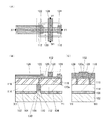
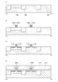
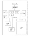
本実施の形態では、半導体装置の一形態を、図1乃至図4を用いて説明する。本実施の形態では、半導体装置の一例として積層型の半導体装置の断面図を示す。
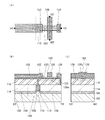
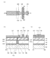
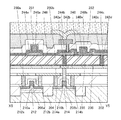
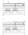
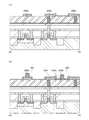
本実施の形態では、実施の形態1に示す半導体装置と異なる形態であり、より詳細な構成について図5を用いて説明し、その後、図6乃至図11を用いて図5に示した半導体装置の作製方法について説明する。
本実施の形態では、実施の形態2の図5に示す半導体装置を使用し、電力が供給されない状況でも記憶内容の保持が可能で、且つ書き込み回数にも制限が無い半導体装置の回路構成の一例について説明する。
本実施の形態では、実施の形態2で示した半導体装置及び実施の形態3で示した回路構成を用い、複数の回路により構成された記憶処理装置について、図13を用いて説明を行う。
本実施の形態では、本発明の一態様の半導体装置を記憶回路に適用し、記憶回路の一例であるCPUの構成について説明する。
本実施の形態においては、本発明の一態様に係る半導体装置を用いることで、消費電力の低い電子機器について説明を行う。
104 ソース領域
106 ドレイン領域
108 第1のチャネル形成領域
110 第1のゲート絶縁膜
112 第1のゲート電極
114 層間絶縁膜
115 酸素バリア膜
116 酸化物絶縁膜
117 バックゲート電極
118 酸素バリア膜
120 酸化物半導体膜
120a 第2のチャネル形成領域
121 酸化物半導体膜
121a 第2のチャネル形成領域
122 ソース電極
123 酸素バリア膜
124 ドレイン電極
126 第2のゲート絶縁膜
127 第2のゲート絶縁膜
128 第2のゲート電極
129 第2のゲート電極
150 第1のトランジスタ
152 第2のトランジスタ
160 第1のトランジスタ
162 第2のトランジスタ
170 第1のトランジスタ
172 第2のトランジスタ
180 第1のトランジスタ
182 第2のトランジスタ
202 半導体基板
204 素子分離領域
206 pウェル領域
208a 第1のゲート絶縁膜
208b 第1のゲート絶縁膜
210a 第1のゲート電極
210b 第1のゲート電極
212 第1のチャネル形成領域
212a ソース領域
212b ドレイン領域
214 第1のチャネル形成領域
214a ソース領域
214b ドレイン領域
216 絶縁膜
218 絶縁膜
220a コンタクトプラグ
220b コンタクトプラグ
220c コンタクトプラグ
220d コンタクトプラグ
222a 絶縁膜
222d 絶縁膜
224a 配線
224c 配線
226a 絶縁膜
226b 絶縁膜
228 コンタクトプラグ
232 配線
234a 絶縁膜
234b 絶縁膜
236 酸素バリア膜
238 酸化物絶縁膜
240 酸化物半導体膜
240a 第2のチャネル形成領域
242 酸素バリア膜
242a 酸素バリア膜
242b 酸素バリア膜
242c 酸素バリア膜
242d 酸素バリア膜
244a 電極
244b ソース電極
244c ドレイン電極
246 第2のゲート絶縁膜
248a 電極
248b 第2のゲート電極
250 絶縁膜
252 絶縁膜
254 電極
256a 絶縁膜
256b 絶縁膜
258 配線
260 絶縁膜
280a 第1のp型トランジスタ
280b 第1のn型トランジスタ
280c 第1のn型トランジスタ
281 容量素子
282 第2のトランジスタ
350 記憶処理装置
351 演算回路
352 演算回路
353 記憶回路
354 記憶回路
355 記憶回路
356 制御回路
357 電源制御回路
901 RF回路
902 アナログベースバンド回路
903 デジタルベースバンド回路
904 バッテリー
905 電源回路
906 アプリケーションプロセッサ
907 CPU
908 DSP
910 フラッシュメモリ
911 ディスプレイコントローラ
912 メモリ回路
913 ディスプレイ
914 表示部
915 ソースドライバ
916 ゲートドライバ
917 音声回路
918 キーボード
919 タッチセンサ
1001 バッテリー
1002 電源回路
1003 マイクロプロセッサ
1004 フラッシュメモリ
1005 音声回路
1006 キーボード
1007 メモリ回路
1008 タッチパネル
1009 ディスプレイ
1010 ディスプレイコントローラ
1011 CPU
1012 DSP
1013 インターフェース
9900 基板
9901 ALU
9902 ALU・Controller
9903 Instruction・Decoder
9904 Interrupt・Controller
9905 Timing・Controller
9906 Register
9907 Register・Controller
9908 Bus・I/F
9909 ROM
9920 ROM・I/F
Claims (10)
- 第1の半導体材料により形成された第1のチャネル形成領域を含む第1のトランジスタと、
前記第1のトランジスタの上方に設けられ、第2の半導体材料により形成された第2のチャネル形成領域を含む第2のトランジスタと、
前記第1のトランジスタと前記第2のトランジスタの間に設けられた酸化物絶縁膜と、を有し、
前記酸化物絶縁膜は、少なくとも前記第2のチャネル形成領域と接して設けられ、
前記第2のチャネル形成領域の外周に、前記酸化物絶縁膜を貫通する酸素バリア膜を有する
ことを特徴とする半導体装置。 - 第1の半導体材料により形成された第1のチャネル形成領域と、
前記第1のチャネル形成領域上に形成された第1のゲート絶縁膜と、
前記第1のゲート絶縁膜と接し、前記第1のチャネル形成領域と重畳する位置に形成された第1のゲート電極と、
前記第1のチャネル形成領域を挟むように形成されたソース領域及びドレイン領域と、を含む第1のトランジスタと、
第2の半導体材料により形成された第2のチャネル形成領域と、
前記第2のチャネル形成領域上に形成された第2のゲート絶縁膜と、
前記第2のゲート絶縁膜と接し、前記第2のチャネル形成領域と重畳する位置に形成された第2のゲート電極と、
前記第2のチャネル形成領域と電気的に接続されたソース電極及びドレイン電極と、
を含む第2のトランジスタと、
前記第1のトランジスタと前記第2のトランジスタの間に設けられた酸化物絶縁膜と、を有し、
前記酸化物絶縁膜は、少なくとも前記第2のチャネル形成領域と接して設けられ、
前記第2のチャネル形成領域の外周に、前記酸化物絶縁膜を貫通する酸素バリア膜を有する
ことを特徴とする半導体装置。 - 請求項1または請求項2において、
さらに、前記第2のトランジスタと同一平面上に設けられた容量素子を、有する
ことを特徴とする半導体装置。 - 請求項1乃至請求項3のいずれか一において、
前記酸化物絶縁膜を貫通して、前記第1のトランジスタと前記第2のトランジスタを電気的に接続する接続電極を、有する
ことを特徴とする半導体装置。 - 請求項4において、
前記接続電極は、前記酸素バリア膜と接して設けられる
ことを特徴とする半導体装置。 - 請求項1乃至請求項5のいずれか一において、
前記酸素バリア膜は、アルミニウム、ルテニウム、イリジウム、ハフニウム、及びタンタルの中から選ばれた金属膜、金属酸化膜、または金属窒化膜である
ことを特徴とする半導体装置。 - 請求項1乃至請求項6のいずれか一において、
前記第1の半導体材料は、シリコンを含む材料である
ことを特徴とする半導体装置。 - 請求項1乃至請求項7のいずれか一において、
前記第2の半導体材料は、酸化物半導体である
ことを特徴とする半導体装置。 - 請求項8において、
前記酸化物半導体膜は、少なくともインジウムまたは亜鉛を含む
ことを特徴とする半導体装置。 - 請求項1乃至請求項9のいずれか一に記載の半導体装置を有する電子機器。
Priority Applications (1)
| Application Number | Priority Date | Filing Date | Title |
|---|---|---|---|
| JP2013065395A JP6081838B2 (ja) | 2012-03-28 | 2013-03-27 | 半導体装置、及び当該半導体装置を有する電子機器 |
Applications Claiming Priority (3)
| Application Number | Priority Date | Filing Date | Title |
|---|---|---|---|
| JP2012073827 | 2012-03-28 | ||
| JP2012073827 | 2012-03-28 | ||
| JP2013065395A JP6081838B2 (ja) | 2012-03-28 | 2013-03-27 | 半導体装置、及び当該半導体装置を有する電子機器 |
Related Child Applications (1)
| Application Number | Title | Priority Date | Filing Date |
|---|---|---|---|
| JP2017007420A Division JP6330065B2 (ja) | 2012-03-28 | 2017-01-19 | 半導体装置 |
Publications (3)
| Publication Number | Publication Date |
|---|---|
| JP2013229587A true JP2013229587A (ja) | 2013-11-07 |
| JP2013229587A5 JP2013229587A5 (ja) | 2016-03-31 |
| JP6081838B2 JP6081838B2 (ja) | 2017-02-15 |
Family
ID=49547958
Family Applications (4)
| Application Number | Title | Priority Date | Filing Date |
|---|---|---|---|
| JP2013065395A Expired - Fee Related JP6081838B2 (ja) | 2012-03-28 | 2013-03-27 | 半導体装置、及び当該半導体装置を有する電子機器 |
| JP2017007420A Expired - Fee Related JP6330065B2 (ja) | 2012-03-28 | 2017-01-19 | 半導体装置 |
| JP2018082170A Active JP6630394B2 (ja) | 2012-03-28 | 2018-04-23 | 半導体装置 |
| JP2019221355A Withdrawn JP2020039004A (ja) | 2012-03-28 | 2019-12-06 | 半導体装置 |
Family Applications After (3)
| Application Number | Title | Priority Date | Filing Date |
|---|---|---|---|
| JP2017007420A Expired - Fee Related JP6330065B2 (ja) | 2012-03-28 | 2017-01-19 | 半導体装置 |
| JP2018082170A Active JP6630394B2 (ja) | 2012-03-28 | 2018-04-23 | 半導体装置 |
| JP2019221355A Withdrawn JP2020039004A (ja) | 2012-03-28 | 2019-12-06 | 半導体装置 |
Country Status (2)
| Country | Link |
|---|---|
| US (2) | US9349849B2 (ja) |
| JP (4) | JP6081838B2 (ja) |
Cited By (9)
| Publication number | Priority date | Publication date | Assignee | Title |
|---|---|---|---|---|
| WO2015097589A1 (en) * | 2013-12-26 | 2015-07-02 | Semiconductor Energy Laboratory Co., Ltd. | Semiconductor device |
| JP2015179839A (ja) * | 2014-02-28 | 2015-10-08 | 株式会社半導体エネルギー研究所 | 半導体装置、該半導体装置を有する表示装置、該表示装置を有する表示モジュール、並びに該半導体装置、該表示装置、及び該表示モジュールを有する電子機器 |
| JP2016001722A (ja) * | 2014-04-08 | 2016-01-07 | 株式会社半導体エネルギー研究所 | 半導体装置及び該半導体装置を含む電子機器 |
| JP2016006855A (ja) * | 2014-05-30 | 2016-01-14 | 株式会社半導体エネルギー研究所 | 半導体装置とその作製方法、電子機器 |
| WO2017072627A1 (ja) * | 2015-10-28 | 2017-05-04 | 株式会社半導体エネルギー研究所 | 半導体装置、モジュール、電子機器および半導体装置の作製方法 |
| JP2017183718A (ja) * | 2016-03-25 | 2017-10-05 | 株式会社半導体エネルギー研究所 | トランジスタ、半導体装置、および電子機器 |
| JP2020057807A (ja) * | 2014-05-27 | 2020-04-09 | 株式会社半導体エネルギー研究所 | 半導体装置 |
| JP2022028780A (ja) * | 2013-10-22 | 2022-02-16 | 株式会社半導体エネルギー研究所 | 半導体装置 |
| JP2022082655A (ja) * | 2015-01-16 | 2022-06-02 | 株式会社半導体エネルギー研究所 | 半導体装置 |
Families Citing this family (17)
| Publication number | Priority date | Publication date | Assignee | Title |
|---|---|---|---|---|
| TWI614813B (zh) | 2013-01-21 | 2018-02-11 | 半導體能源研究所股份有限公司 | 半導體裝置的製造方法 |
| TWI631711B (zh) * | 2013-05-01 | 2018-08-01 | 半導體能源研究所股份有限公司 | 半導體裝置 |
| JP2015032717A (ja) * | 2013-08-02 | 2015-02-16 | 株式会社東芝 | 固体撮像装置およびカメラモジュール |
| WO2015060133A1 (en) | 2013-10-22 | 2015-04-30 | Semiconductor Energy Laboratory Co., Ltd. | Semiconductor device |
| KR102529174B1 (ko) | 2013-12-27 | 2023-05-08 | 가부시키가이샤 한도오따이 에네루기 켄큐쇼 | 반도체 장치 |
| CN104167448B (zh) * | 2014-08-05 | 2017-06-30 | 京东方科技集团股份有限公司 | 薄膜晶体管及其制备方法、阵列基板和显示装置 |
| US9722091B2 (en) | 2014-09-12 | 2017-08-01 | Semiconductor Energy Laboratory Co., Ltd. | Method for manufacturing semiconductor device |
| TWI732383B (zh) | 2015-02-06 | 2021-07-01 | 日商半導體能源研究所股份有限公司 | 裝置及其製造方法以及電子裝置 |
| KR102582523B1 (ko) | 2015-03-19 | 2023-09-26 | 가부시키가이샤 한도오따이 에네루기 켄큐쇼 | 반도체 장치 및 전자 기기 |
| JP2016225614A (ja) * | 2015-05-26 | 2016-12-28 | 株式会社半導体エネルギー研究所 | 半導体装置 |
| US10978489B2 (en) | 2015-07-24 | 2021-04-13 | Semiconductor Energy Laboratory Co., Ltd. | Semiconductor device, display panel, method for manufacturing semiconductor device, method for manufacturing display panel, and information processing device |
| TW202236685A (zh) | 2015-10-30 | 2022-09-16 | 日商半導體能源研究所股份有限公司 | 電容器、半導體裝置、模組以及電子裝置的製造方法 |
| WO2017103737A1 (en) | 2015-12-18 | 2017-06-22 | Semiconductor Energy Laboratory Co., Ltd. | Display panel, input/output device, data processing device, and method for manufacturing display panel |
| US9666491B1 (en) * | 2016-06-16 | 2017-05-30 | United Microelectronics Corp. | Method of forming semiconductor device |
| KR102596126B1 (ko) * | 2016-10-19 | 2023-10-31 | 삼성디스플레이 주식회사 | 표시 장치 및 그 제조방법 |
| JP7293190B2 (ja) | 2018-03-16 | 2023-06-19 | 株式会社半導体エネルギー研究所 | 半導体装置 |
| KR20210085942A (ko) * | 2019-12-31 | 2021-07-08 | 엘지디스플레이 주식회사 | 박막 트랜지스터 및 이를 포함하는 표시장치 |
Citations (5)
| Publication number | Priority date | Publication date | Assignee | Title |
|---|---|---|---|---|
| JP2008270313A (ja) * | 2007-04-17 | 2008-11-06 | Matsushita Electric Ind Co Ltd | 半導体記憶素子 |
| JP2010114413A (ja) * | 2008-10-08 | 2010-05-20 | Sony Corp | 薄膜トランジスタおよび表示装置 |
| JP2011243976A (ja) * | 2010-04-23 | 2011-12-01 | Semiconductor Energy Lab Co Ltd | 半導体装置の作製方法 |
| JP2012015498A (ja) * | 2010-06-04 | 2012-01-19 | Semiconductor Energy Lab Co Ltd | 半導体装置 |
| JP2012053971A (ja) * | 2010-08-06 | 2012-03-15 | Semiconductor Energy Lab Co Ltd | 半導体装置 |
Family Cites Families (131)
| Publication number | Priority date | Publication date | Assignee | Title |
|---|---|---|---|---|
| JPS60198861A (ja) | 1984-03-23 | 1985-10-08 | Fujitsu Ltd | 薄膜トランジスタ |
| JPH0244256B2 (ja) | 1987-01-28 | 1990-10-03 | Kagaku Gijutsucho Mukizaishitsu Kenkyushocho | Ingazn2o5deshimesarerurotsuhoshokeinosojokozoojusurukagobutsuoyobisonoseizoho |
| JPH0244258B2 (ja) | 1987-02-24 | 1990-10-03 | Kagaku Gijutsucho Mukizaishitsu Kenkyushocho | Ingazn3o6deshimesarerurotsuhoshokeinosojokozoojusurukagobutsuoyobisonoseizoho |
| JPS63210023A (ja) | 1987-02-24 | 1988-08-31 | Natl Inst For Res In Inorg Mater | InGaZn↓4O↓7で示される六方晶系の層状構造を有する化合物およびその製造法 |
| JPH0244260B2 (ja) | 1987-02-24 | 1990-10-03 | Kagaku Gijutsucho Mukizaishitsu Kenkyushocho | Ingazn5o8deshimesarerurotsuhoshokeinosojokozoojusurukagobutsuoyobisonoseizoho |
| JPH0244262B2 (ja) | 1987-02-27 | 1990-10-03 | Kagaku Gijutsucho Mukizaishitsu Kenkyushocho | Ingazn6o9deshimesarerurotsuhoshokeinosojokozoojusurukagobutsuoyobisonoseizoho |
| JPH0244263B2 (ja) | 1987-04-22 | 1990-10-03 | Kagaku Gijutsucho Mukizaishitsu Kenkyushocho | Ingazn7o10deshimesarerurotsuhoshokeinosojokozoojusurukagobutsuoyobisonoseizoho |
| JPH05251705A (ja) | 1992-03-04 | 1993-09-28 | Fuji Xerox Co Ltd | 薄膜トランジスタ |
| JP3479375B2 (ja) | 1995-03-27 | 2003-12-15 | 科学技術振興事業団 | 亜酸化銅等の金属酸化物半導体による薄膜トランジスタとpn接合を形成した金属酸化物半導体装置およびそれらの製造方法 |
| DE69635107D1 (de) | 1995-08-03 | 2005-09-29 | Koninkl Philips Electronics Nv | Halbleiteranordnung mit einem transparenten schaltungselement |
| JP3625598B2 (ja) | 1995-12-30 | 2005-03-02 | 三星電子株式会社 | 液晶表示装置の製造方法 |
| JPH11145138A (ja) | 1997-11-10 | 1999-05-28 | Hitachi Ltd | 半導体装置およびその製造方法 |
| JP4170454B2 (ja) | 1998-07-24 | 2008-10-22 | Hoya株式会社 | 透明導電性酸化物薄膜を有する物品及びその製造方法 |
| JP2000150861A (ja) | 1998-11-16 | 2000-05-30 | Tdk Corp | 酸化物薄膜 |
| JP3276930B2 (ja) | 1998-11-17 | 2002-04-22 | 科学技術振興事業団 | トランジスタ及び半導体装置 |
| TW460731B (en) | 1999-09-03 | 2001-10-21 | Ind Tech Res Inst | Electrode structure and production method of wide viewing angle LCD |
| JP4089858B2 (ja) | 2000-09-01 | 2008-05-28 | 国立大学法人東北大学 | 半導体デバイス |
| KR20020038482A (ko) | 2000-11-15 | 2002-05-23 | 모리시타 요이찌 | 박막 트랜지스터 어레이, 그 제조방법 및 그것을 이용한표시패널 |
| JP3997731B2 (ja) | 2001-03-19 | 2007-10-24 | 富士ゼロックス株式会社 | 基材上に結晶性半導体薄膜を形成する方法 |
| JP2002289859A (ja) | 2001-03-23 | 2002-10-04 | Minolta Co Ltd | 薄膜トランジスタ |
| JP2002289810A (ja) | 2001-03-28 | 2002-10-04 | Toshiba Corp | 半導体装置およびその製造方法 |
| JP4090716B2 (ja) | 2001-09-10 | 2008-05-28 | 雅司 川崎 | 薄膜トランジスタおよびマトリクス表示装置 |
| JP3925839B2 (ja) | 2001-09-10 | 2007-06-06 | シャープ株式会社 | 半導体記憶装置およびその試験方法 |
| EP1443130B1 (en) | 2001-11-05 | 2011-09-28 | Japan Science and Technology Agency | Natural superlattice homologous single crystal thin film, method for preparation thereof, and device using said single crystal thin film |
| JP4164562B2 (ja) | 2002-09-11 | 2008-10-15 | 独立行政法人科学技術振興機構 | ホモロガス薄膜を活性層として用いる透明薄膜電界効果型トランジスタ |
| JP4083486B2 (ja) | 2002-02-21 | 2008-04-30 | 独立行政法人科学技術振興機構 | LnCuO(S,Se,Te)単結晶薄膜の製造方法 |
| US7049190B2 (en) | 2002-03-15 | 2006-05-23 | Sanyo Electric Co., Ltd. | Method for forming ZnO film, method for forming ZnO semiconductor layer, method for fabricating semiconductor device, and semiconductor device |
| JP3933591B2 (ja) | 2002-03-26 | 2007-06-20 | 淳二 城戸 | 有機エレクトロルミネッセント素子 |
| US7339187B2 (en) | 2002-05-21 | 2008-03-04 | State Of Oregon Acting By And Through The Oregon State Board Of Higher Education On Behalf Of Oregon State University | Transistor structures |
| JP2004022625A (ja) | 2002-06-13 | 2004-01-22 | Murata Mfg Co Ltd | 半導体デバイス及び該半導体デバイスの製造方法 |
| US7105868B2 (en) | 2002-06-24 | 2006-09-12 | Cermet, Inc. | High-electron mobility transistor with zinc oxide |
| US6611449B1 (en) | 2002-09-24 | 2003-08-26 | Infineon Technologies Aktiengesellschaft | Contact for memory cells |
| US7067843B2 (en) | 2002-10-11 | 2006-06-27 | E. I. Du Pont De Nemours And Company | Transparent oxide semiconductor thin film transistors |
| JP2004241690A (ja) | 2003-02-07 | 2004-08-26 | Oki Electric Ind Co Ltd | スタック型セル及びその製造方法 |
| JP4166105B2 (ja) | 2003-03-06 | 2008-10-15 | シャープ株式会社 | 半導体装置およびその製造方法 |
| JP2004273732A (ja) | 2003-03-07 | 2004-09-30 | Sharp Corp | アクティブマトリクス基板およびその製造方法 |
| JP2004281965A (ja) * | 2003-03-19 | 2004-10-07 | Matsushita Electric Ind Co Ltd | 半導体装置及びその製造方法 |
| JP3930453B2 (ja) | 2003-05-06 | 2007-06-13 | 株式会社東芝 | 半導体装置 |
| JP4108633B2 (ja) | 2003-06-20 | 2008-06-25 | シャープ株式会社 | 薄膜トランジスタおよびその製造方法ならびに電子デバイス |
| KR100725690B1 (ko) * | 2003-07-08 | 2007-06-07 | 마츠시타 덴끼 산교 가부시키가이샤 | 반도체장치 및 그 제조방법 |
| US7262463B2 (en) | 2003-07-25 | 2007-08-28 | Hewlett-Packard Development Company, L.P. | Transistor including a deposited channel region having a doped portion |
| JP2005101213A (ja) | 2003-09-24 | 2005-04-14 | Toshiba Corp | 半導体装置の製造方法 |
| JP4357289B2 (ja) | 2003-12-26 | 2009-11-04 | Okiセミコンダクタ株式会社 | 半導体装置の製造方法及び半導体装置 |
| US7282782B2 (en) | 2004-03-12 | 2007-10-16 | Hewlett-Packard Development Company, L.P. | Combined binary oxide semiconductor device |
| US7297977B2 (en) | 2004-03-12 | 2007-11-20 | Hewlett-Packard Development Company, L.P. | Semiconductor device |
| US7145174B2 (en) | 2004-03-12 | 2006-12-05 | Hewlett-Packard Development Company, Lp. | Semiconductor device |
| EP2246894B2 (en) | 2004-03-12 | 2018-10-10 | Japan Science and Technology Agency | Method for fabricating a thin film transistor having an amorphous oxide as a channel layer |
| JP2005327989A (ja) | 2004-05-17 | 2005-11-24 | Toshiba Corp | 半導体装置及びその製造方法 |
| US7211825B2 (en) | 2004-06-14 | 2007-05-01 | Yi-Chi Shih | Indium oxide-based thin film transistors and circuits |
| JP2006100760A (ja) | 2004-09-02 | 2006-04-13 | Casio Comput Co Ltd | 薄膜トランジスタおよびその製造方法 |
| US7285501B2 (en) | 2004-09-17 | 2007-10-23 | Hewlett-Packard Development Company, L.P. | Method of forming a solution processed device |
| US7298084B2 (en) | 2004-11-02 | 2007-11-20 | 3M Innovative Properties Company | Methods and displays utilizing integrated zinc oxide row and column drivers in conjunction with organic light emitting diodes |
| KR100998527B1 (ko) | 2004-11-10 | 2010-12-07 | 고쿠리츠다이가쿠호진 토쿄고교 다이가꾸 | 비정질 산화물 및 전계 효과 트랜지스터 |
| US7453065B2 (en) | 2004-11-10 | 2008-11-18 | Canon Kabushiki Kaisha | Sensor and image pickup device |
| US7829444B2 (en) | 2004-11-10 | 2010-11-09 | Canon Kabushiki Kaisha | Field effect transistor manufacturing method |
| RU2358354C2 (ru) | 2004-11-10 | 2009-06-10 | Кэнон Кабусики Кайся | Светоизлучающее устройство |
| US7791072B2 (en) | 2004-11-10 | 2010-09-07 | Canon Kabushiki Kaisha | Display |
| US7863611B2 (en) | 2004-11-10 | 2011-01-04 | Canon Kabushiki Kaisha | Integrated circuits utilizing amorphous oxides |
| JP5118812B2 (ja) | 2004-11-10 | 2013-01-16 | キヤノン株式会社 | 電界効果型トランジスタ |
| US7579224B2 (en) | 2005-01-21 | 2009-08-25 | Semiconductor Energy Laboratory Co., Ltd. | Method for manufacturing a thin film semiconductor device |
| TWI562380B (en) | 2005-01-28 | 2016-12-11 | Semiconductor Energy Lab Co Ltd | Semiconductor device, electronic device, and method of manufacturing semiconductor device |
| US7608531B2 (en) | 2005-01-28 | 2009-10-27 | Semiconductor Energy Laboratory Co., Ltd. | Semiconductor device, electronic device, and method of manufacturing semiconductor device |
| US7858451B2 (en) | 2005-02-03 | 2010-12-28 | Semiconductor Energy Laboratory Co., Ltd. | Electronic device, semiconductor device and manufacturing method thereof |
| US7948171B2 (en) | 2005-02-18 | 2011-05-24 | Semiconductor Energy Laboratory Co., Ltd. | Light emitting device |
| US20060197092A1 (en) | 2005-03-03 | 2006-09-07 | Randy Hoffman | System and method for forming conductive material on a substrate |
| US8681077B2 (en) | 2005-03-18 | 2014-03-25 | Semiconductor Energy Laboratory Co., Ltd. | Semiconductor device, and display device, driving method and electronic apparatus thereof |
| WO2006105077A2 (en) | 2005-03-28 | 2006-10-05 | Massachusetts Institute Of Technology | Low voltage thin film transistor with high-k dielectric material |
| US7645478B2 (en) | 2005-03-31 | 2010-01-12 | 3M Innovative Properties Company | Methods of making displays |
| US8300031B2 (en) | 2005-04-20 | 2012-10-30 | Semiconductor Energy Laboratory Co., Ltd. | Semiconductor device comprising transistor having gate and drain connected through a current-voltage conversion element |
| JP2006344849A (ja) | 2005-06-10 | 2006-12-21 | Casio Comput Co Ltd | 薄膜トランジスタ |
| US7402506B2 (en) | 2005-06-16 | 2008-07-22 | Eastman Kodak Company | Methods of making thin film transistors comprising zinc-oxide-based semiconductor materials and transistors made thereby |
| US7691666B2 (en) | 2005-06-16 | 2010-04-06 | Eastman Kodak Company | Methods of making thin film transistors comprising zinc-oxide-based semiconductor materials and transistors made thereby |
| US7507618B2 (en) | 2005-06-27 | 2009-03-24 | 3M Innovative Properties Company | Method for making electronic devices using metal oxide nanoparticles |
| KR100711890B1 (ko) | 2005-07-28 | 2007-04-25 | 삼성에스디아이 주식회사 | 유기 발광표시장치 및 그의 제조방법 |
| JP2007059128A (ja) | 2005-08-23 | 2007-03-08 | Canon Inc | 有機el表示装置およびその製造方法 |
| JP4850457B2 (ja) | 2005-09-06 | 2012-01-11 | キヤノン株式会社 | 薄膜トランジスタ及び薄膜ダイオード |
| JP5116225B2 (ja) | 2005-09-06 | 2013-01-09 | キヤノン株式会社 | 酸化物半導体デバイスの製造方法 |
| JP2007073705A (ja) | 2005-09-06 | 2007-03-22 | Canon Inc | 酸化物半導体チャネル薄膜トランジスタおよびその製造方法 |
| JP4280736B2 (ja) | 2005-09-06 | 2009-06-17 | キヤノン株式会社 | 半導体素子 |
| JP5078246B2 (ja) | 2005-09-29 | 2012-11-21 | 株式会社半導体エネルギー研究所 | 半導体装置、及び半導体装置の作製方法 |
| EP1998375A3 (en) | 2005-09-29 | 2012-01-18 | Semiconductor Energy Laboratory Co, Ltd. | Semiconductor device having oxide semiconductor layer and manufacturing method |
| JP5064747B2 (ja) | 2005-09-29 | 2012-10-31 | 株式会社半導体エネルギー研究所 | 半導体装置、電気泳動表示装置、表示モジュール、電子機器、及び半導体装置の作製方法 |
| JP5037808B2 (ja) | 2005-10-20 | 2012-10-03 | キヤノン株式会社 | アモルファス酸化物を用いた電界効果型トランジスタ、及び該トランジスタを用いた表示装置 |
| KR101358954B1 (ko) | 2005-11-15 | 2014-02-06 | 가부시키가이샤 한도오따이 에네루기 켄큐쇼 | 다이오드 및 액티브 매트릭스 표시장치 |
| US20070114616A1 (en) * | 2005-11-23 | 2007-05-24 | Dirk Manger | Field effect transistor and method of manufacturing the same |
| TWI292281B (en) | 2005-12-29 | 2008-01-01 | Ind Tech Res Inst | Pixel structure of active organic light emitting diode and method of fabricating the same |
| US7365009B2 (en) * | 2006-01-04 | 2008-04-29 | United Microelectronics Corp. | Structure of metal interconnect and fabrication method thereof |
| US7867636B2 (en) | 2006-01-11 | 2011-01-11 | Murata Manufacturing Co., Ltd. | Transparent conductive film and method for manufacturing the same |
| JP4977478B2 (ja) | 2006-01-21 | 2012-07-18 | 三星電子株式会社 | ZnOフィルム及びこれを用いたTFTの製造方法 |
| US7576394B2 (en) | 2006-02-02 | 2009-08-18 | Kochi Industrial Promotion Center | Thin film transistor including low resistance conductive thin films and manufacturing method thereof |
| US7977169B2 (en) | 2006-02-15 | 2011-07-12 | Kochi Industrial Promotion Center | Semiconductor device including active layer made of zinc oxide with controlled orientations and manufacturing method thereof |
| KR20070101595A (ko) | 2006-04-11 | 2007-10-17 | 삼성전자주식회사 | ZnO TFT |
| US20070252928A1 (en) | 2006-04-28 | 2007-11-01 | Toppan Printing Co., Ltd. | Structure, transmission type liquid crystal display, reflection type display and manufacturing method thereof |
| JP5028033B2 (ja) | 2006-06-13 | 2012-09-19 | キヤノン株式会社 | 酸化物半導体膜のドライエッチング方法 |
| JP4882548B2 (ja) * | 2006-06-30 | 2012-02-22 | 富士通セミコンダクター株式会社 | 半導体装置及びその製造方法 |
| JP4609797B2 (ja) | 2006-08-09 | 2011-01-12 | Nec液晶テクノロジー株式会社 | 薄膜デバイス及びその製造方法 |
| JP4999400B2 (ja) | 2006-08-09 | 2012-08-15 | キヤノン株式会社 | 酸化物半導体膜のドライエッチング方法 |
| JP4332545B2 (ja) | 2006-09-15 | 2009-09-16 | キヤノン株式会社 | 電界効果型トランジスタ及びその製造方法 |
| JP4274219B2 (ja) | 2006-09-27 | 2009-06-03 | セイコーエプソン株式会社 | 電子デバイス、有機エレクトロルミネッセンス装置、有機薄膜半導体装置 |
| JP5164357B2 (ja) | 2006-09-27 | 2013-03-21 | キヤノン株式会社 | 半導体装置及び半導体装置の製造方法 |
| US7622371B2 (en) | 2006-10-10 | 2009-11-24 | Hewlett-Packard Development Company, L.P. | Fused nanocrystal thin film semiconductor and method |
| US7772021B2 (en) | 2006-11-29 | 2010-08-10 | Samsung Electronics Co., Ltd. | Flat panel displays comprising a thin-film transistor having a semiconductive oxide in its channel and methods of fabricating the same for use in flat panel displays |
| JP2008140684A (ja) | 2006-12-04 | 2008-06-19 | Toppan Printing Co Ltd | カラーelディスプレイおよびその製造方法 |
| KR101303578B1 (ko) | 2007-01-05 | 2013-09-09 | 삼성전자주식회사 | 박막 식각 방법 |
| US8207063B2 (en) | 2007-01-26 | 2012-06-26 | Eastman Kodak Company | Process for atomic layer deposition |
| KR100851215B1 (ko) | 2007-03-14 | 2008-08-07 | 삼성에스디아이 주식회사 | 박막 트랜지스터 및 이를 이용한 유기 전계 발광표시장치 |
| US7795613B2 (en) | 2007-04-17 | 2010-09-14 | Toppan Printing Co., Ltd. | Structure with transistor |
| KR101325053B1 (ko) | 2007-04-18 | 2013-11-05 | 삼성디스플레이 주식회사 | 박막 트랜지스터 기판 및 이의 제조 방법 |
| KR20080094300A (ko) | 2007-04-19 | 2008-10-23 | 삼성전자주식회사 | 박막 트랜지스터 및 그 제조 방법과 박막 트랜지스터를포함하는 평판 디스플레이 |
| KR101334181B1 (ko) | 2007-04-20 | 2013-11-28 | 삼성전자주식회사 | 선택적으로 결정화된 채널층을 갖는 박막 트랜지스터 및 그제조 방법 |
| CN101663762B (zh) | 2007-04-25 | 2011-09-21 | 佳能株式会社 | 氧氮化物半导体 |
| KR101334182B1 (ko) * | 2007-05-28 | 2013-11-28 | 삼성전자주식회사 | ZnO 계 박막 트랜지스터의 제조방법 |
| KR101345376B1 (ko) | 2007-05-29 | 2013-12-24 | 삼성전자주식회사 | ZnO 계 박막 트랜지스터 및 그 제조방법 |
| US8202365B2 (en) | 2007-12-17 | 2012-06-19 | Fujifilm Corporation | Process for producing oriented inorganic crystalline film, and semiconductor device using the oriented inorganic crystalline film |
| US7943988B2 (en) * | 2008-09-05 | 2011-05-17 | Freescale Semiconductor, Inc. | Power MOSFET with a gate structure of different material |
| JP4623179B2 (ja) | 2008-09-18 | 2011-02-02 | ソニー株式会社 | 薄膜トランジスタおよびその製造方法 |
| JP5451280B2 (ja) | 2008-10-09 | 2014-03-26 | キヤノン株式会社 | ウルツ鉱型結晶成長用基板およびその製造方法ならびに半導体装置 |
| CN105762152B (zh) * | 2009-10-29 | 2021-03-09 | 株式会社半导体能源研究所 | 半导体器件 |
| EP2494692B1 (en) * | 2009-10-30 | 2016-11-23 | Semiconductor Energy Laboratory Co. Ltd. | Logic circuit and semiconductor device |
| IN2012DN04871A (ja) * | 2009-12-11 | 2015-09-25 | Semiconductor Energy Laoboratory Co Ltd | |
| KR101913111B1 (ko) * | 2009-12-18 | 2018-10-31 | 가부시키가이샤 한도오따이 에네루기 켄큐쇼 | 반도체 장치 |
| CN104700890B (zh) * | 2009-12-18 | 2017-10-17 | 株式会社半导体能源研究所 | 非易失性锁存电路和逻辑电路以及使用它们的半导体器件 |
| WO2011080999A1 (en) * | 2009-12-28 | 2011-07-07 | Semiconductor Energy Laboratory Co., Ltd. | Semiconductor device |
| US8415731B2 (en) | 2010-01-20 | 2013-04-09 | Semiconductor Energy Laboratory Co., Ltd. | Semiconductor storage device with integrated capacitor and having transistor overlapping sections |
| KR20120120330A (ko) | 2010-01-29 | 2012-11-01 | 가부시키가이샤 한도오따이 에네루기 켄큐쇼 | 반도체 장치 |
| DE112011100841B4 (de) * | 2010-03-08 | 2021-11-25 | Semiconductor Energy Laboratory Co., Ltd. | Halbleitervorrichtung und verfahren zur herstellung der halbleitervorrichtung |
| KR101850567B1 (ko) | 2010-07-16 | 2018-04-19 | 가부시키가이샤 한도오따이 에네루기 켄큐쇼 | 반도체 장치 |
| TWI570920B (zh) | 2011-01-26 | 2017-02-11 | 半導體能源研究所股份有限公司 | 半導體裝置及其製造方法 |
| TWI620328B (zh) | 2011-01-26 | 2018-04-01 | 半導體能源研究所股份有限公司 | 半導體裝置及其製造方法 |
| US9012905B2 (en) | 2011-04-08 | 2015-04-21 | Semiconductor Energy Laboratory Co., Ltd. | Semiconductor device including transistor comprising oxide semiconductor and method for manufacturing the same |
| US9093538B2 (en) * | 2011-04-08 | 2015-07-28 | Semiconductor Energy Laboratory Co., Ltd. | Semiconductor device and method for manufacturing the same |
-
2013
- 2013-03-15 US US13/833,342 patent/US9349849B2/en active Active
- 2013-03-27 JP JP2013065395A patent/JP6081838B2/ja not_active Expired - Fee Related
-
2016
- 2016-04-26 US US15/138,539 patent/US10249766B2/en active Active
-
2017
- 2017-01-19 JP JP2017007420A patent/JP6330065B2/ja not_active Expired - Fee Related
-
2018
- 2018-04-23 JP JP2018082170A patent/JP6630394B2/ja active Active
-
2019
- 2019-12-06 JP JP2019221355A patent/JP2020039004A/ja not_active Withdrawn
Patent Citations (5)
| Publication number | Priority date | Publication date | Assignee | Title |
|---|---|---|---|---|
| JP2008270313A (ja) * | 2007-04-17 | 2008-11-06 | Matsushita Electric Ind Co Ltd | 半導体記憶素子 |
| JP2010114413A (ja) * | 2008-10-08 | 2010-05-20 | Sony Corp | 薄膜トランジスタおよび表示装置 |
| JP2011243976A (ja) * | 2010-04-23 | 2011-12-01 | Semiconductor Energy Lab Co Ltd | 半導体装置の作製方法 |
| JP2012015498A (ja) * | 2010-06-04 | 2012-01-19 | Semiconductor Energy Lab Co Ltd | 半導体装置 |
| JP2012053971A (ja) * | 2010-08-06 | 2012-03-15 | Semiconductor Energy Lab Co Ltd | 半導体装置 |
Cited By (18)
| Publication number | Priority date | Publication date | Assignee | Title |
|---|---|---|---|---|
| JP2022028780A (ja) * | 2013-10-22 | 2022-02-16 | 株式会社半導体エネルギー研究所 | 半導体装置 |
| JP7084540B2 (ja) | 2013-10-22 | 2022-06-14 | 株式会社半導体エネルギー研究所 | 半導体装置 |
| TWI701806B (zh) * | 2013-12-26 | 2020-08-11 | 日商半導體能源研究所股份有限公司 | 半導體裝置 |
| US9466615B2 (en) | 2013-12-26 | 2016-10-11 | Semiconductor Energy Laboratory Co., Ltd. | Semiconductor device |
| TWI673853B (zh) * | 2013-12-26 | 2019-10-01 | 日商半導體能源研究所股份有限公司 | 半導體裝置 |
| WO2015097589A1 (en) * | 2013-12-26 | 2015-07-02 | Semiconductor Energy Laboratory Co., Ltd. | Semiconductor device |
| JP2020113779A (ja) * | 2014-02-28 | 2020-07-27 | 株式会社半導体エネルギー研究所 | 半導体装置 |
| JP2015179839A (ja) * | 2014-02-28 | 2015-10-08 | 株式会社半導体エネルギー研究所 | 半導体装置、該半導体装置を有する表示装置、該表示装置を有する表示モジュール、並びに該半導体装置、該表示装置、及び該表示モジュールを有する電子機器 |
| US10693014B2 (en) | 2014-02-28 | 2020-06-23 | Semiconductor Energy Laboratory Co., Ltd. | Semiconductor device, display device including the semiconductor device, display module including the display device, and electronic appliance including the semiconductor device, the display device, and the display module |
| JP2016001722A (ja) * | 2014-04-08 | 2016-01-07 | 株式会社半導体エネルギー研究所 | 半導体装置及び該半導体装置を含む電子機器 |
| JP2020057807A (ja) * | 2014-05-27 | 2020-04-09 | 株式会社半導体エネルギー研究所 | 半導体装置 |
| US10658389B2 (en) | 2014-05-30 | 2020-05-19 | Semiconductor Energy Laboratory Co., Ltd. | Semiconductor device, manufacturing method thereof, and electronic device |
| JP2016006855A (ja) * | 2014-05-30 | 2016-01-14 | 株式会社半導体エネルギー研究所 | 半導体装置とその作製方法、電子機器 |
| JP2020161822A (ja) * | 2014-05-30 | 2020-10-01 | 株式会社半導体エネルギー研究所 | 半導体装置 |
| US11282860B2 (en) | 2014-05-30 | 2022-03-22 | Semiconductor Energy Laboratory Co., Ltd. | Semiconductor device, manufacturing method thereof, and electronic device |
| JP2022082655A (ja) * | 2015-01-16 | 2022-06-02 | 株式会社半導体エネルギー研究所 | 半導体装置 |
| WO2017072627A1 (ja) * | 2015-10-28 | 2017-05-04 | 株式会社半導体エネルギー研究所 | 半導体装置、モジュール、電子機器および半導体装置の作製方法 |
| JP2017183718A (ja) * | 2016-03-25 | 2017-10-05 | 株式会社半導体エネルギー研究所 | トランジスタ、半導体装置、および電子機器 |
Also Published As
| Publication number | Publication date |
|---|---|
| US10249766B2 (en) | 2019-04-02 |
| JP2017103474A (ja) | 2017-06-08 |
| JP2018117158A (ja) | 2018-07-26 |
| US9349849B2 (en) | 2016-05-24 |
| US20130299818A1 (en) | 2013-11-14 |
| JP6081838B2 (ja) | 2017-02-15 |
| JP2020039004A (ja) | 2020-03-12 |
| JP6630394B2 (ja) | 2020-01-15 |
| US20160240685A1 (en) | 2016-08-18 |
| JP6330065B2 (ja) | 2018-05-23 |
Similar Documents
| Publication | Publication Date | Title |
|---|---|---|
| JP6330065B2 (ja) | 半導体装置 | |
| JP6600063B2 (ja) | 半導体装置 | |
| JP6487088B2 (ja) | 半導体装置の作製方法 | |
| KR102493701B1 (ko) | 반도체 장치, 및 그 제작 방법 | |
| US9236428B2 (en) | Semiconductor element, method for manufacturing the semiconductor element, and semiconductor device including the semiconductor element | |
| JP6427211B2 (ja) | 半導体装置 | |
| US20130270616A1 (en) | Semiconductor device | |
| JP6049479B2 (ja) | 半導体装置 | |
| JP6553693B2 (ja) | 半導体装置 | |
| JP7474369B2 (ja) | 半導体装置 | |
| JP6088852B2 (ja) | 半導体装置の作製方法、及び半導体装置 | |
| JP6753986B2 (ja) | 半導体装置 | |
| JP6212153B2 (ja) | 半導体装置 |
Legal Events
| Date | Code | Title | Description |
|---|---|---|---|
| A521 | Request for written amendment filed |
Free format text: JAPANESE INTERMEDIATE CODE: A523 Effective date: 20160215 |
|
| A621 | Written request for application examination |
Free format text: JAPANESE INTERMEDIATE CODE: A621 Effective date: 20160215 |
|
| A977 | Report on retrieval |
Free format text: JAPANESE INTERMEDIATE CODE: A971007 Effective date: 20161227 |
|
| TRDD | Decision of grant or rejection written | ||
| A01 | Written decision to grant a patent or to grant a registration (utility model) |
Free format text: JAPANESE INTERMEDIATE CODE: A01 Effective date: 20170110 |
|
| A61 | First payment of annual fees (during grant procedure) |
Free format text: JAPANESE INTERMEDIATE CODE: A61 Effective date: 20170119 |
|
| R150 | Certificate of patent or registration of utility model |
Ref document number: 6081838 Country of ref document: JP Free format text: JAPANESE INTERMEDIATE CODE: R150 |
|
| R250 | Receipt of annual fees |
Free format text: JAPANESE INTERMEDIATE CODE: R250 |
|
| LAPS | Cancellation because of no payment of annual fees |