JP2011514597A - 変化するシート抵抗を有するタッチスクリーンセンサ - Google Patents
変化するシート抵抗を有するタッチスクリーンセンサ Download PDFInfo
- Publication number
- JP2011514597A JP2011514597A JP2010548859A JP2010548859A JP2011514597A JP 2011514597 A JP2011514597 A JP 2011514597A JP 2010548859 A JP2010548859 A JP 2010548859A JP 2010548859 A JP2010548859 A JP 2010548859A JP 2011514597 A JP2011514597 A JP 2011514597A
- Authority
- JP
- Japan
- Prior art keywords
- micropattern
- area
- conductive
- sheet resistance
- touch screen
- Prior art date
- Legal status (The legal status is an assumption and is not a legal conclusion. Google has not performed a legal analysis and makes no representation as to the accuracy of the status listed.)
- Withdrawn
Links
Images


Classifications
-
- G—PHYSICS
- G06—COMPUTING; CALCULATING OR COUNTING
- G06F—ELECTRIC DIGITAL DATA PROCESSING
- G06F3/00—Input arrangements for transferring data to be processed into a form capable of being handled by the computer; Output arrangements for transferring data from processing unit to output unit, e.g. interface arrangements
- G06F3/01—Input arrangements or combined input and output arrangements for interaction between user and computer
- G06F3/03—Arrangements for converting the position or the displacement of a member into a coded form
- G06F3/041—Digitisers, e.g. for touch screens or touch pads, characterised by the transducing means
- G06F3/044—Digitisers, e.g. for touch screens or touch pads, characterised by the transducing means by capacitive means
-
- C—CHEMISTRY; METALLURGY
- C23—COATING METALLIC MATERIAL; COATING MATERIAL WITH METALLIC MATERIAL; CHEMICAL SURFACE TREATMENT; DIFFUSION TREATMENT OF METALLIC MATERIAL; COATING BY VACUUM EVAPORATION, BY SPUTTERING, BY ION IMPLANTATION OR BY CHEMICAL VAPOUR DEPOSITION, IN GENERAL; INHIBITING CORROSION OF METALLIC MATERIAL OR INCRUSTATION IN GENERAL
- C23F—NON-MECHANICAL REMOVAL OF METALLIC MATERIAL FROM SURFACE; INHIBITING CORROSION OF METALLIC MATERIAL OR INCRUSTATION IN GENERAL; MULTI-STEP PROCESSES FOR SURFACE TREATMENT OF METALLIC MATERIAL INVOLVING AT LEAST ONE PROCESS PROVIDED FOR IN CLASS C23 AND AT LEAST ONE PROCESS COVERED BY SUBCLASS C21D OR C22F OR CLASS C25
- C23F1/00—Etching metallic material by chemical means
- C23F1/02—Local etching
-
- C—CHEMISTRY; METALLURGY
- C23—COATING METALLIC MATERIAL; COATING MATERIAL WITH METALLIC MATERIAL; CHEMICAL SURFACE TREATMENT; DIFFUSION TREATMENT OF METALLIC MATERIAL; COATING BY VACUUM EVAPORATION, BY SPUTTERING, BY ION IMPLANTATION OR BY CHEMICAL VAPOUR DEPOSITION, IN GENERAL; INHIBITING CORROSION OF METALLIC MATERIAL OR INCRUSTATION IN GENERAL
- C23F—NON-MECHANICAL REMOVAL OF METALLIC MATERIAL FROM SURFACE; INHIBITING CORROSION OF METALLIC MATERIAL OR INCRUSTATION IN GENERAL; MULTI-STEP PROCESSES FOR SURFACE TREATMENT OF METALLIC MATERIAL INVOLVING AT LEAST ONE PROCESS PROVIDED FOR IN CLASS C23 AND AT LEAST ONE PROCESS COVERED BY SUBCLASS C21D OR C22F OR CLASS C25
- C23F1/00—Etching metallic material by chemical means
- C23F1/10—Etching compositions
- C23F1/14—Aqueous compositions
-
- G—PHYSICS
- G01—MEASURING; TESTING
- G01R—MEASURING ELECTRIC VARIABLES; MEASURING MAGNETIC VARIABLES
- G01R27/00—Arrangements for measuring resistance, reactance, impedance, or electric characteristics derived therefrom
- G01R27/02—Measuring real or complex resistance, reactance, impedance, or other two-pole characteristics derived therefrom, e.g. time constant
- G01R27/26—Measuring inductance or capacitance; Measuring quality factor, e.g. by using the resonance method; Measuring loss factor; Measuring dielectric constants ; Measuring impedance or related variables
- G01R27/2605—Measuring capacitance
-
- G—PHYSICS
- G06—COMPUTING; CALCULATING OR COUNTING
- G06F—ELECTRIC DIGITAL DATA PROCESSING
- G06F3/00—Input arrangements for transferring data to be processed into a form capable of being handled by the computer; Output arrangements for transferring data from processing unit to output unit, e.g. interface arrangements
- G06F3/01—Input arrangements or combined input and output arrangements for interaction between user and computer
- G06F3/03—Arrangements for converting the position or the displacement of a member into a coded form
- G06F3/041—Digitisers, e.g. for touch screens or touch pads, characterised by the transducing means
- G06F3/044—Digitisers, e.g. for touch screens or touch pads, characterised by the transducing means by capacitive means
- G06F3/0446—Digitisers, e.g. for touch screens or touch pads, characterised by the transducing means by capacitive means using a grid-like structure of electrodes in at least two directions, e.g. using row and column electrodes
-
- G—PHYSICS
- G06—COMPUTING; CALCULATING OR COUNTING
- G06F—ELECTRIC DIGITAL DATA PROCESSING
- G06F3/00—Input arrangements for transferring data to be processed into a form capable of being handled by the computer; Output arrangements for transferring data from processing unit to output unit, e.g. interface arrangements
- G06F3/01—Input arrangements or combined input and output arrangements for interaction between user and computer
- G06F3/03—Arrangements for converting the position or the displacement of a member into a coded form
- G06F3/041—Digitisers, e.g. for touch screens or touch pads, characterised by the transducing means
- G06F3/045—Digitisers, e.g. for touch screens or touch pads, characterised by the transducing means using resistive elements, e.g. a single continuous surface or two parallel surfaces put in contact
-
- G—PHYSICS
- G06—COMPUTING; CALCULATING OR COUNTING
- G06F—ELECTRIC DIGITAL DATA PROCESSING
- G06F2203/00—Indexing scheme relating to G06F3/00 - G06F3/048
- G06F2203/041—Indexing scheme relating to G06F3/041 - G06F3/045
- G06F2203/04108—Touchless 2D- digitiser, i.e. digitiser detecting the X/Y position of the input means, finger or stylus, also when it does not touch, but is proximate to the digitiser's interaction surface without distance measurement in the Z direction
-
- G—PHYSICS
- G06—COMPUTING; CALCULATING OR COUNTING
- G06F—ELECTRIC DIGITAL DATA PROCESSING
- G06F2203/00—Indexing scheme relating to G06F3/00 - G06F3/048
- G06F2203/041—Indexing scheme relating to G06F3/041 - G06F3/045
- G06F2203/04112—Electrode mesh in capacitive digitiser: electrode for touch sensing is formed of a mesh of very fine, normally metallic, interconnected lines that are almost invisible to see. This provides a quite large but transparent electrode surface, without need for ITO or similar transparent conductive material
-
- G—PHYSICS
- G06—COMPUTING; CALCULATING OR COUNTING
- G06F—ELECTRIC DIGITAL DATA PROCESSING
- G06F3/00—Input arrangements for transferring data to be processed into a form capable of being handled by the computer; Output arrangements for transferring data from processing unit to output unit, e.g. interface arrangements
- G06F3/01—Input arrangements or combined input and output arrangements for interaction between user and computer
- G06F3/03—Arrangements for converting the position or the displacement of a member into a coded form
- G06F3/041—Digitisers, e.g. for touch screens or touch pads, characterised by the transducing means
- G06F3/0412—Digitisers structurally integrated in a display
Abstract
【選択図】図18
Description
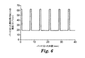
以下の記載による金薄膜の微小パターンが、無色のガラスの薄いシート(およそ1mmの厚さ)上に堆積される。微小パターン240が、図3及び図4に表される。金層の厚さ又は高さは、約100ナノメートルである。マイクロパターン240は、水平の細い配線242を含む一連の水平(x軸)メッシュバー241を伴い、配線242は、幅がおよそ2マイクロメートルである。これらの水平メッシュ配線242の4本が、より大きな構造の接触パッド260と電気に接続している。メッシュバーは、幅がおよそ6mmであった。したがって、13本の等間隔な配線244が、6mmの幅(y軸)を横断し、13本の等間隔な配線242が6mmの長さ(x軸)を横断し、配線の正方形グリッドのピッチは500マイクロメートルである。図4に描かれているように、いくつかの配線は、およそ25マイクロメートル(場所の特定の容易化のために、図では誇張されている)の断絶部250を有する。500マイクロメートルピッチにおける、2マイクロメートル幅の不透明配線を有する正方形グリッドでは、不透明配線の空間占有率は、0.80%であり、したがって、99.20%の開口をもたらす。同じ正方形グリッドであるが、500マイクロメートル毎に25マイクロメートルの断絶部を有するものでは、空間占有率は0.78%であり、したがって、99.22%の開口をもたらす。したがって、この設計は、99.22%の開口を有する1mm×6mm区域、及び99.20%の開口を有する6mm×6mm区域を含む。メッシュを有するガラス物品の平均可視透過率は、およそ0.92×0.992=91%である(0.92という係数は、パターンの導電体が堆積されていない領域における光透過率の界面反射損失に関連する)。水平バー方向に沿って、4本の金の配線によって互いに接続された、一連の完全なグリッド区域が存在する。スパッタ金薄膜に関し、5E−06Ωcmの実効バルク抵抗値を想定すると、2マイクロメートル幅、500マイクロメートル長の金薄膜の区分は、およそ125Ωの抵抗率を有する。完成したグリッドを有する区域は、バーの方向に電流が流れるために、およそ115Ω/スクエアの有効シート抵抗を有する。完成したグリッドを有する区域を接続する4本の配線は、区域間において、およそ62.5Ωの抵抗率を生じる。導電配線要素の上記の配置は、図6にプロットされるように、バー方向に沿って、空間的に異なる単位長さ当たりの抵抗を生じる。図5は、水平メッシュバーの配列の、同等の回路を例示する回路は、レジスタによって接続される、一連のプレートを有する。
以下の記載による金薄膜の微小パターンが、無色のガラスの薄いシート(およそ1ミリメートルの厚さ)上に堆積される。微小パターン340が、図7に描かれている。金の厚さは、約100ナノメートルである。微小パターン340は、一連の交互配置された楔形又は三角形の形状の透明導電性区域を有する。各楔形は、細い金属の配線342、344で作製されるメッシュからなり、配線342、344(図7a〜7c参照)は、およそ2マイクロメートルの幅である。メッシュの楔形は、その底辺においておよそ1センチメートルの幅であり、長さはおよそ6センチメートルである。配線342、344の正方形グリッドのピッチは、500マイクロメートルである。楔形内のメッシュの選択される区域(図7a〜図7b参照)内において、およそ25マイクロメートル長の断絶部350が、楔形内の局部的面抵抗(その長軸に沿って通過する電流のため)に影響を与えるように、意図的に設置される。図7a及び図7bに描かれているように、区域7a、及び7b(図7では、区域はおよそ1センチメートルで分離している)、断絶部350は、長軸方向において、シート抵抗を1.2倍超増加させるメッシュに含まれる。全体的な設計はまた、区域7c(図7cに描かれている)を含み、これは、区域7a及び7bから、電気的に絶縁され、離間しており、また区域7a及び7bのものよりも低いシート抵抗値のメッシュを有する。メッシュ区域7cは、99.20%の開口を有し、一方でメッシュ区域7a及び7bは、それぞれ、99.20%及び99.21%の開口率を有する。全体的な設計はまた、区域7a、7b、及び7cよりも大きなピッチのメッシュを有するが、同じ幅の配線を有する、区域7d及び7e(図7d及び7eに描かれている)を含み、より高いシート抵抗及び可視光透過率をもたらす。
タッチスクリーンセンサのための透明センサ素子400が、図9に例示される。センサ素子400は、互いに積層され、明確にするために図9では分離されて描かれている、パターン化された2つの導電層410、414(例えば、X軸層、及びY軸層)、光学的に透明な2つの接着剤層412、416、及び基部プレート418を含む。層410及び414は、透明導電メッシュバーを含み、ここで一方の層はx軸方向に配向され、他方の層はy軸方向に配向されている(図2参照)。基部プレート418は、面積が6センチメートル×6センチメートル、厚さが1mmのガラスのシートである。好適な、光学的に透明な接着剤は、ミネソタ州セントポールの3M Company製の、Optically Clear Laminating Adhesive 8141である。X層及びY層のそれぞれに関し、金属の微小パターンを有する透明なポリマーフィルムが使用される。以下の記載による金薄膜の微小パターンが、PETの薄いシート上に堆積される。好適なPET基材としては、厚さおよそ125マイクロメートルの、デラウェア州ウィルミントンのDuPont製のST504 PETが挙げられる。
タッチスクリーンセンサのための透明センサ素子が記載される。図9に描かれているように、センサ素子は、パターン化された2つの導電層、光学的に透明な2つの接着剤層、及び基部プレートを含む。基部プレートは、図9に描かれるように互いに積層される、面積が6センチメートル×6センチメートル、かつ厚さが1mmである、ガラスのシートである。好適な、光学的に透明な接着剤は、3M Company製の、Optically Clear Laminating Adhesive 8141である。X層及びY層のそれぞれに関し、金属の微小パターンを有する透明なポリマーフィルムが使用される。以下の記載による金薄膜の微小パターンが、PETの薄いシート上に堆積される。好適なPET基材としては、厚さおよそ125マイクロメートルの、DuPont製のST504 PETが挙げられる。
タッチスクリーンセンサのための透明センサ素子が記載される。図9に描かれているように、センサ素子は、パターン化された2つの導電層、光学的に透明な2つの接着剤層、及び基部プレートを含む。基部プレートは、図9に描かれるように互いに積層される、面積が6センチメートル×6センチメートル、かつ厚さが1mmである、ガラスのシートである。好適な、光学的に透明な接着剤は、3M Company製の、Optically Clear Laminating Adhesive 8141である。X層及びY層のそれぞれに関し、金属の微小パターンを有する透明なポリマーフィルムが使用される。以下の記載による金薄膜の微小パターンが、PETの薄いシート上に堆積される。好適なPET基材としては、厚さおよそ125マイクロメートルの、DuPont製のST504 PETが挙げられる。
同一出願人による米国特許仮出願第61/032,273号に記載されるマイクロコンタクト印刷及びエッチングを使用して、透明センサ素子が製作され、図16、図17、及び図18に概して示されるタッチセンサ駆動装置と組み合わされた。装置は次に、ディスプレイと接続されたコンピューター処理ユニットと一体化されて、装置を試験した。装置は、複数の、単独の又は同時的な指接触の位置を検出することができ、これは、ディスプレイに図形的に示された。
第1のパターン化された基材
厚さ125マイクロメートル(μm)を有するポリエチレンテレフタレート(PET)から作製される第1の可視光基材が、熱蒸着コーターを使用して、100nmの銀薄膜で蒸気コーティングされて、第1の銀金属化フィルムを生成した。PETは、デラウェア州ウィルミントンのE.I.du Pont de Nemoursから、製品番号ST504として市販されていた。銀は、ウィスコンシン州ミルウォーキーのCerac Inc.から、99.99%純度の3mmショットとして市販されていた。
第2のパターン化された基材は、第2の可視光基材を使用する第1のパターン化された基材として作製されて、第2の銀金属化フィルムを製造した。第2の非連続的な六角形メッシュパターンの間に置かれた、第2の連続的な六角形メッシュパターンを有する第2スタンプが製造された。
2層投影型静電容量タッチスクリーン透明センサ素子を製造するために、上記で作製された第1及び第2のパターン化された基材が、以下のように使用された。
透明センサ素子が、タッチセンサ駆動装置に接続された。ガラス表面に指接触が成された際、コンピューターモニターは、接触感知区域内で生じている接触の位置を、モニターの対応する位置における色の変化(白色から緑色)の形態でレンダリングした。ガラス表面に指2本の接触が同時に成された際、コンピューターモニターは、接触感知区域内で生じている接触の位置を、モニターの対応する位置における色の変化(白色から緑色)の形態でレンダリングした。ガラス表面に指3本の接触が同時に成された際、コンピューターモニターは、接触感知区域内で生じている接触の位置を、モニターの対応する位置における色の変化(白色から緑色)の形態でレンダリングした。
Claims (20)
- 可視光透明基材と、
前記可視光透明基材の上又は中に配置される導電性微小パターンであって、前記微小パターンは、接触感知領域内の第1区域微小パターン及び第2区域微小パターンを含む、導電性微小パターンと、
を含み、
前記第1区域微小パターンは、第1の方向において、第1シート抵抗値を有し、可視光透明であり、少なくとも90%の開口を有し、
前記第2区域微小パターンは、前記第1の方向において、第2シート抵抗値を有し、
前記第1シート抵抗値は、前記第2シート抵抗値とは異なる、タッチスクリーンセンサ。 - 前記第1区域微小パターンが、前記第2区域微小パターンと電気的に接触していない、請求項1に記載のタッチスクリーンセンサ。
- 前記第1区域微小パターンが、前記第2区域微小パターンと電気的に接触している、請求項1に記載のタッチスクリーンセンサ。
- 前記第1区域微小パターン及び第2区域微小パターンが、前記感知領域にわたって延びる、電気的に接触する金属の微小パターンメッシュの部分である、請求項1に記載のタッチスクリーンセンサ。
- 前記第1区域微小パターンのシート抵抗値が、前記第1区域微小パターン内の少なくとも1つの経路に沿って変化する、請求項1に記載のタッチスクリーンセンサ。
- 前記第1区域微小パターンのシート抵抗値が、0.1〜1000Ω/スクエアの範囲である、請求項1に記載のタッチスクリーンセンサ。
- 前記導電性微小パターンが、前記接触感知領域内で、95%〜99.5%の開口を有する、請求項1に記載のタッチスクリーンセンサ。
- 前記導電性微小パターンが、前記感知領域内に前記タッチスクリーンセンサの駆動装置から電気的に絶縁された導電性堆積物を含む、請求項1に記載のタッチスクリーンセンサ。
- 前記導電性微小パターンが、0.5〜5マイクロメートルの範囲の値の幅、及び前記感知領域内に1マイクロメートル未満の均一な厚さを有する線形金属構造を含む、請求項1に記載のタッチスクリーンセンサ。
- 前記導電性微小パターンが、導電配線を含む二次元メッシュを含み、いくつかの配線が選択的に配置された断絶部を含む、請求項1に記載のタッチスクリーンセンサ。
- 可視光透明基材と、
前記可視光透明基材の上又は中に配置される導電性微小パターンであって、前記微小パターンは、接触感知領域内に第1区域微小パターンを含む、導電性微小パターンと、
を含み、
前記第1区域微小パターンは、異方性第1シート抵抗を有し、可視光透明であり、少なくとも90%の開口を有する、タッチスクリーンセンサ。 - 前記感知領域内に、前記第1区域微小パターンと電気的に接触しない第2区域微小パターンを更に含み、前記第2区域微小パターンは、異方性第2シート抵抗を有し、可視光透明であり、少なくとも90%の開口を有する、請求項11に記載のタッチスクリーンセンサ。
- 前記感知領域内に、前記第1区域微小パターンと電気的に接触しない第2区域微小パターンを更に含み、前記第2区域微小パターンは、等方性第2シート抵抗を有し、可視光透明であり、少なくとも90%の開口を有する、請求項11に記載のタッチスクリーンセンサ。
- 前記第1区域微小パターンが異方性第1シート抵抗を有し、直交方向において、少なくとも1.5倍のシート抵抗値の差を有し、95%〜99.5%の開口を有する、請求項11に記載のタッチスクリーンセンサ。
- 少なくとも一方向における前記第1区域微小パターンのシート抵抗値が、前記第1区域微小パターン内の少なくとも一方向に沿って変化する、請求項11に記載のタッチスクリーンセンサ。
- 前記第1区域微小パターンのシート抵抗値が、0.1〜1000Ω/スクエアの範囲である、請求項11に記載のタッチスクリーンセンサ。
- 前記導電性微小パターンが、前記タッチスクリーンセンサの駆動装置から電気的に絶縁された導電性堆積物を含む、請求項11に記載のタッチスクリーンセンサ。
- 前記導電性微小パターンが、0.5〜5マイクロメートルの範囲の値の幅、及び前記感知領域内に1マイクロメートル未満の均一な厚さを有する線形金属構造を含む、請求項11に記載のタッチスクリーンセンサ。
- 可視光透明基材と、
前記可視光透明基材の上又は中に配置される導電性微小パターンであって、前記微小パターンは、
接触感知領域内の第1区域微小パターン及び第2区域微小パターンを含み、
前記導電性微小パターンは、500ナノメートル未満の厚さ、及び0.5〜5マイクロメートルの幅を有する金属の線形導電性構造を含み、
前記第1区域微小パターンは、第1の方向において5〜500Ω/スクエアの第1シート抵抗値を有し、可視光透明であり、95%〜99.5%の開口を有し、
前記第2区域微小パターンは、前記第1の方向において、第2シート抵抗値を有する、導電性微小パターンと、
を含み、
前記第1シート抵抗値は、前記第2シート抵抗値とは異なる、タッチスクリーンセンサ。 - 可視光透明基材と、
前記可視光透明基材の上又は中に配置される導電性微小パターンであって、前記微小パターンは、
接触感知領域内に第1区域微小パターンを含み、
前記導電性微小パターンは、500ナノメートル未満の厚さ、及び0.5〜5マイクロメートルの幅を有する金属の線形導電性構造を含み、
前記第1区域微小パターンは、直交方向において、少なくとも1.5倍のシート抵抗値の差を有する異方性第1シート抵抗を有し、可視光透明であり、95%〜99.5%の開口を有する、導電性微小パターンと、
を含む、タッチスクリーンセンサ。
Applications Claiming Priority (3)
| Application Number | Priority Date | Filing Date | Title |
|---|---|---|---|
| US3227308P | 2008-02-28 | 2008-02-28 | |
| US3226908P | 2008-02-28 | 2008-02-28 | |
| PCT/US2009/035264 WO2009108765A2 (en) | 2008-02-28 | 2009-02-26 | Touch screen sensor having varying sheet resistance |
Related Child Applications (1)
| Application Number | Title | Priority Date | Filing Date |
|---|---|---|---|
| JP2014185974A Division JP6247184B2 (ja) | 2008-02-28 | 2014-09-12 | 変化するシート抵抗を有するタッチスクリーンセンサ |
Publications (2)
| Publication Number | Publication Date |
|---|---|
| JP2011514597A true JP2011514597A (ja) | 2011-05-06 |
| JP2011514597A5 JP2011514597A5 (ja) | 2012-03-29 |
Family
ID=41016705
Family Applications (4)
| Application Number | Title | Priority Date | Filing Date |
|---|---|---|---|
| JP2010548859A Withdrawn JP2011514597A (ja) | 2008-02-28 | 2009-02-26 | 変化するシート抵抗を有するタッチスクリーンセンサ |
| JP2014185974A Active JP6247184B2 (ja) | 2008-02-28 | 2014-09-12 | 変化するシート抵抗を有するタッチスクリーンセンサ |
| JP2016029895A Active JP6096953B2 (ja) | 2008-02-28 | 2016-02-19 | 変化するシート抵抗を有するタッチスクリーンセンサ |
| JP2017019588A Active JP6291095B2 (ja) | 2008-02-28 | 2017-02-06 | 変化するシート抵抗を有するタッチスクリーンセンサ |
Family Applications After (3)
| Application Number | Title | Priority Date | Filing Date |
|---|---|---|---|
| JP2014185974A Active JP6247184B2 (ja) | 2008-02-28 | 2014-09-12 | 変化するシート抵抗を有するタッチスクリーンセンサ |
| JP2016029895A Active JP6096953B2 (ja) | 2008-02-28 | 2016-02-19 | 変化するシート抵抗を有するタッチスクリーンセンサ |
| JP2017019588A Active JP6291095B2 (ja) | 2008-02-28 | 2017-02-06 | 変化するシート抵抗を有するタッチスクリーンセンサ |
Country Status (6)
| Country | Link |
|---|---|
| US (15) | US8274494B2 (ja) |
| EP (2) | EP2863295B1 (ja) |
| JP (4) | JP2011514597A (ja) |
| CN (1) | CN102016768B (ja) |
| TW (1) | TWI435255B (ja) |
| WO (1) | WO2009108765A2 (ja) |
Cited By (9)
| Publication number | Priority date | Publication date | Assignee | Title |
|---|---|---|---|---|
| JP2012198879A (ja) * | 2011-03-08 | 2012-10-18 | Fujifilm Corp | 抵抗膜式マルチタッチパネル及び抵抗膜式マルチタッチパネルに用いる電極シート |
| JP2013058195A (ja) * | 2011-09-07 | 2013-03-28 | Tpk Touch Solutions (Xiamen) Inc | タッチ感知電極及びタッチパネル |
| WO2013111795A1 (ja) * | 2012-01-24 | 2013-08-01 | デクセリアルズ株式会社 | 透明導電性素子、入力装置、電子機器および透明導電性素子作製用原盤 |
| JP2013173342A (ja) * | 2012-01-24 | 2013-09-05 | Dexerials Corp | 透明導電性素子およびその製造方法、入力装置、電子機器、ならびに透明導電層の加工方法 |
| JP2015153002A (ja) * | 2014-02-12 | 2015-08-24 | 三菱電機株式会社 | タッチスクリーン、タッチパネル、表示素子および電子機器 |
| WO2015141473A1 (ja) * | 2014-03-20 | 2015-09-24 | アルプス電気株式会社 | 静電容量式センサ |
| JP2016028335A (ja) * | 2015-09-28 | 2016-02-25 | デクセリアルズ株式会社 | 透明電極素子、情報入力装置、および電子機器 |
| WO2016148036A1 (ja) * | 2015-03-14 | 2016-09-22 | コニカミノルタ株式会社 | 導電性パターン、導電性パターンの製造方法、タッチパネル及び液晶表示装置 |
| JP2018152122A (ja) * | 2013-02-27 | 2018-09-27 | ミラエナノテック カンパニー リミテッド | 静電容量方式タッチスクリーンのためのダミーパターンを使用するタッチパッドの構造 |
Families Citing this family (121)
| Publication number | Priority date | Publication date | Assignee | Title |
|---|---|---|---|---|
| EP2863295B1 (en) | 2008-02-28 | 2019-10-16 | 3M Innovative Properties Company | Touch screen sensor having varying sheet resistance |
| KR101080183B1 (ko) * | 2008-04-04 | 2011-11-07 | (주)멜파스 | 가장자리 위치 인식 특성이 개선된 접촉 감지 장치 |
| CN101673162A (zh) * | 2008-04-10 | 2010-03-17 | 爱特梅尔公司 | 具有噪声抑制的电容性触摸屏幕 |
| US9069418B2 (en) * | 2008-06-06 | 2015-06-30 | Apple Inc. | High resistivity metal fan out |
| US8288005B2 (en) | 2008-07-31 | 2012-10-16 | 3M Innovative Properties Company | Fluoropolymer compositions and method of making and using thereof |
| CN102164999B (zh) * | 2008-07-31 | 2014-05-14 | 3M创新有限公司 | 叠氮化物组合物及其制备和使用方法 |
| US9244568B2 (en) * | 2008-11-15 | 2016-01-26 | Atmel Corporation | Touch screen sensor |
| EP2401669B1 (en) | 2009-02-26 | 2016-04-06 | 3M Innovative Properties Company | Touch screen sensor and patterned substrate having overlaid micropatterns with low visibility |
| TWI390281B (zh) * | 2009-06-05 | 2013-03-21 | Higgstec Inc | 微電極矩陣與具有微電極矩陣之觸控面板 |
| CN102803562B (zh) | 2009-06-25 | 2015-09-30 | 3M创新有限公司 | 湿式蚀刻自组装单层图案化基材和金属图案化制品的方法 |
| EP2449547B1 (en) | 2009-06-30 | 2016-09-21 | 3M Innovative Properties Company | Electronic displays and metal micropatterned substrates having a graphic |
| CN101943965B (zh) * | 2009-07-08 | 2013-09-18 | 群康科技(深圳)有限公司 | 触摸屏及具有触摸屏的电子装置 |
| CN101943967B (zh) * | 2009-07-08 | 2012-08-15 | 群康科技(深圳)有限公司 | 触摸屏的定位方法 |
| TWI395006B (zh) * | 2009-09-09 | 2013-05-01 | Au Optronics Corp | 觸控顯示面板 |
| CN102033669B (zh) * | 2009-09-24 | 2013-08-14 | 群康科技(深圳)有限公司 | 电容式触控面板 |
| KR101082607B1 (ko) | 2009-10-16 | 2011-11-10 | 엘지이노텍 주식회사 | 터치패널용 면상 부재 및 그 제조 방법 |
| US8766105B2 (en) * | 2009-11-20 | 2014-07-01 | Fujifilm Corporation | Conductive sheet, method for using conductive sheet, and capacitive touch panel |
| JP2012014669A (ja) | 2009-11-20 | 2012-01-19 | Fujifilm Corp | 導電シート、導電シートの使用方法及び静電容量方式タッチパネル |
| JP5676225B2 (ja) | 2009-11-24 | 2015-02-25 | 富士フイルム株式会社 | 導電シート、導電シートの使用方法及び静電容量方式タッチパネル |
| EP2530560B1 (en) * | 2010-01-28 | 2019-06-19 | FUJIFILM Corporation | Conductive sheet, method for using conductive sheet, and touch panel |
| TWI471798B (zh) * | 2010-03-12 | 2015-02-01 | Alps Electric Co Ltd | Input device |
| US8941395B2 (en) * | 2010-04-27 | 2015-01-27 | 3M Innovative Properties Company | Integrated passive circuit elements for sensing devices |
| JP5248653B2 (ja) * | 2010-05-27 | 2013-07-31 | 富士フイルム株式会社 | 導電シート及び静電容量方式タッチパネル |
| JP5507343B2 (ja) * | 2010-05-31 | 2014-05-28 | 富士フイルム株式会社 | タッチパネル及び導電シート |
| KR20130109090A (ko) * | 2010-06-11 | 2013-10-07 | 쓰리엠 이노베이티브 프로퍼티즈 컴파니 | 힘 측정을 갖는 포지셔널 터치 센서 |
| CN102314271B (zh) * | 2010-07-07 | 2014-11-05 | 宸鸿科技(厦门)有限公司 | 一种电容式触控图形结构及其制法、触控面板及触控显示装置 |
| US9019207B1 (en) | 2010-09-28 | 2015-04-28 | Google Inc. | Spacebar integrated with trackpad |
| US8754854B1 (en) | 2010-09-28 | 2014-06-17 | Google Inc. | Keyboard integrated with trackpad |
| US9491852B2 (en) | 2010-10-15 | 2016-11-08 | Apple Inc. | Trace border routing |
| KR101680256B1 (ko) * | 2010-11-08 | 2016-12-13 | 삼성디스플레이 주식회사 | 저항막 방식의 터치 스크린 패널 |
| TWI567802B (zh) * | 2010-11-19 | 2017-01-21 | 富士軟片股份有限公司 | 觸控面板、觸控面板的製造方法以及導電膜 |
| US8998099B2 (en) | 2010-12-16 | 2015-04-07 | 3M Innovative Properties Company | Transparent micropatterned RFID antenna and articles incorporating same |
| CN103329643B (zh) | 2011-02-02 | 2016-12-21 | 3M创新有限公司 | 具有变暗的多层导体迹线的图案化基底 |
| US8933906B2 (en) | 2011-02-02 | 2015-01-13 | 3M Innovative Properties Company | Patterned substrates with non-linear conductor traces |
| BR112013020151A2 (pt) | 2011-02-09 | 2016-11-08 | Kinestral Technologies Inc | dispositivos eletrocrômicos de multicamadas com comutação espacialmente coordenada |
| DE102011011769A1 (de) | 2011-02-18 | 2012-08-23 | Fresenius Medical Care Deutschland Gmbh | Medizintechnisches Gerät mit Touchscreen und Verfahren |
| TWI567912B (zh) * | 2011-02-18 | 2017-01-21 | 富士軟片股份有限公司 | 導電片以及觸控面板 |
| WO2013013171A2 (en) | 2011-07-21 | 2013-01-24 | United States Postal Service | Content retrieval systems for distribution items |
| TW201310470A (zh) * | 2011-08-31 | 2013-03-01 | Shih Hua Technology Ltd | 透明導電膜以及使用該透明導電膜的觸控面板 |
| CN102956285A (zh) * | 2011-08-31 | 2013-03-06 | 天津富纳源创科技有限公司 | 透明导电膜以及使用该透明导电膜的触控面板 |
| CN102956284A (zh) * | 2011-08-31 | 2013-03-06 | 天津富纳源创科技有限公司 | 透明导电膜以及使用该透明导电膜的触控面板 |
| CN102955602B (zh) * | 2011-08-31 | 2016-05-18 | 天津富纳源创科技有限公司 | 透明导电膜以及使用该透明导电膜的触控面板 |
| TWI478181B (zh) * | 2011-08-31 | 2015-03-21 | Shih Hua Technology Ltd | 透明導電膜以及使用該透明導電膜的觸控面板 |
| KR101434031B1 (ko) * | 2011-09-27 | 2014-08-27 | 주식회사 엘지화학 | 전도성 패턴을 포함하는 전도성 기판 및 이를 포함하는 터치 패널 |
| US9256311B2 (en) * | 2011-10-28 | 2016-02-09 | Atmel Corporation | Flexible touch sensor |
| KR20130051803A (ko) * | 2011-11-10 | 2013-05-21 | 삼성전기주식회사 | 터치패널 |
| ITVE20110080A1 (it) * | 2011-12-16 | 2013-06-17 | I R C A S P A Ind Resiste Nze Corazzate | Dispositivo di rilevazione di prossimita' e contatto in volanti per autoveicoli |
| EP2765490B1 (en) | 2011-12-16 | 2017-06-07 | FUJIFILM Corporation | Conductive sheet and touch panel |
| JP5777251B2 (ja) * | 2011-12-16 | 2015-09-09 | 富士フイルム株式会社 | タッチパネル用導電シート及びタッチパネル |
| JP5509186B2 (ja) * | 2011-12-16 | 2014-06-04 | 富士フイルム株式会社 | タッチパネル及びタッチパネル用導電シート |
| JP5748647B2 (ja) * | 2011-12-22 | 2015-07-15 | 富士フイルム株式会社 | 導電シート及びタッチパネル |
| TWI479386B (zh) * | 2011-12-23 | 2015-04-01 | Lg Chemical Ltd | 導電基板及包含其之電子裝置 |
| EP2812779A4 (en) | 2012-02-10 | 2015-09-23 | 3M Innovative Properties Co | MESH PATTERN FOR TOUCH SENSOR ELECTRODES |
| TWI467432B (zh) * | 2012-02-17 | 2015-01-01 | E Ink Holdings Inc | 觸控感測模組 |
| US9046974B2 (en) * | 2012-02-28 | 2015-06-02 | Eastman Kodak Company | Transparent touch-screen capacitor with micro-wire electrode |
| US8773392B2 (en) * | 2012-02-28 | 2014-07-08 | Eastman Kodak Company | Transparent touch-responsive capacitor with variable-pattern micro-wires |
| US8884918B2 (en) * | 2012-02-28 | 2014-11-11 | Eastman Kodak Company | Electronic device having metallic micro-wires |
| US8773393B2 (en) * | 2012-02-28 | 2014-07-08 | Eastman Kodak Company | Touch screen with dummy micro-wires |
| US8836668B2 (en) * | 2012-02-28 | 2014-09-16 | Eastman Kodak Company | Transparent touch-responsive capacitor with variable-height micro-wires |
| GB2499987B (en) | 2012-03-02 | 2017-01-11 | Novalia Ltd | Touch-sensitive input device |
| GB2499851B (en) * | 2012-03-02 | 2016-11-02 | Novalia Ltd | Touch-sensitive input device |
| CN104160368B (zh) * | 2012-03-06 | 2017-03-08 | 三菱电机株式会社 | 触摸屏、触摸面板、显示装置以及电子仪器 |
| US9489856B2 (en) | 2012-05-23 | 2016-11-08 | SmartBound Technologies, LLC | Interactive printed article with touch-activated presentation |
| US9552087B2 (en) * | 2012-06-28 | 2017-01-24 | Polyic Gmbh & Co. Kg | Multi-layer body |
| TWI490762B (zh) * | 2012-06-29 | 2015-07-01 | Raydium Semiconductor Corp | 觸控感測裝置及觸控感測方法 |
| JP5224203B1 (ja) | 2012-07-11 | 2013-07-03 | 大日本印刷株式会社 | タッチパネルセンサ、タッチパネル装置および表示装置 |
| WO2014025900A1 (en) * | 2012-08-08 | 2014-02-13 | Kinestral Technologies, Inc. | Electrochromic multi-layer devices with composite electrically conductive layers |
| US9091868B2 (en) | 2012-08-08 | 2015-07-28 | Kinestral Technologies, Inc. | Electrochromic multi-layer devices with composite current modulating structure |
| WO2014025921A1 (en) | 2012-08-08 | 2014-02-13 | Kinestral Technologies, Inc. | Electrochromic multi-layer devices with current modulating structure |
| US9250754B2 (en) | 2012-09-27 | 2016-02-02 | Google Inc. | Pressure-sensitive trackpad |
| JP5607697B2 (ja) * | 2012-10-16 | 2014-10-15 | 日本写真印刷株式会社 | タッチセンサ及び電子機器 |
| US9510456B2 (en) * | 2012-11-09 | 2016-11-29 | Shenzhen O-Film Tech Co., Ltd. | Transparent conductor and preparation method thereof |
| US9229553B2 (en) | 2012-11-30 | 2016-01-05 | 3M Innovative Properties Company | Mesh patterns for touch sensor electrodes |
| US9164607B2 (en) | 2012-11-30 | 2015-10-20 | 3M Innovative Properties Company | Complementary touch panel electrodes |
| TWI552211B (zh) * | 2012-11-30 | 2016-10-01 | 恆顥科技股份有限公司 | 觸控電極裝置 |
| KR102044900B1 (ko) * | 2013-03-07 | 2019-11-15 | 삼성디스플레이 주식회사 | 터치 스크린 패널 |
| US9645695B2 (en) * | 2013-03-07 | 2017-05-09 | Mitsubishi Electric Corporation | Display apparatus |
| US20140262443A1 (en) * | 2013-03-14 | 2014-09-18 | Cambrios Technologies Corporation | Hybrid patterned nanostructure transparent conductors |
| US9639215B2 (en) * | 2013-03-30 | 2017-05-02 | Shenzhen O-Film Tech Co., Ltd. | Touch screen |
| US9089061B2 (en) * | 2013-03-30 | 2015-07-21 | Shenzhen O-Film Tech Co., Ltd. | Conductive film, method for making the same, and touch screen including the same |
| US9538654B2 (en) * | 2013-03-30 | 2017-01-03 | Shenzhen O-Film Tech Co., Ltd. | Conductive film, method for manufacturing the same, and touch screen including the same |
| US20150289421A1 (en) * | 2013-06-20 | 2015-10-08 | Joel Ho | Apparatus for an emp shield for computing devices |
| KR102142855B1 (ko) * | 2013-08-29 | 2020-08-31 | 미래나노텍(주) | 터치스크린 패널용 배선 전극, 이를 이용한 터치스크린 패널 및 그 제조방법 |
| CN104423737A (zh) * | 2013-08-30 | 2015-03-18 | 天津富纳源创科技有限公司 | 电容式触控装置及控制方法 |
| CN104423738A (zh) * | 2013-08-30 | 2015-03-18 | 天津富纳源创科技有限公司 | 电容式触控装置的控制方法 |
| KR20150036903A (ko) * | 2013-09-30 | 2015-04-08 | 엘지이노텍 주식회사 | 터치 윈도우 및 이를 포함하는 디스플레이 장치 |
| US9436304B1 (en) | 2013-11-01 | 2016-09-06 | Google Inc. | Computer with unified touch surface for input |
| TWI510914B (zh) * | 2013-11-19 | 2015-12-01 | Henghao Technology Co Ltd | 觸控面板及其測試裝置 |
| US20160253020A1 (en) | 2013-11-21 | 2016-09-01 | 3M Innovative Properties Company | Electronic device with force detection |
| KR102161743B1 (ko) | 2013-11-26 | 2020-10-06 | 삼성디스플레이 주식회사 | 터치 감지 장치 및 이를 포함하는 표시 장치 |
| CN103926729B (zh) * | 2013-12-31 | 2017-12-22 | 上海天马微电子有限公司 | 一种阵列基板、彩膜基板、触控显示装置及其驱动方法 |
| WO2015122721A1 (ko) | 2014-02-13 | 2015-08-20 | 주식회사 엘지화학 | 마스터 몰드의 제조방법, 이로 제조된 마스터 몰드, 투명포토마스크의 제조방법, 이로 제조된 투명포토마스크 및 상기 투명포토마스크를 이용한 전도성 메쉬패턴의 제조방법 |
| US9454252B2 (en) | 2014-02-14 | 2016-09-27 | Atmel Corporation | Touch-sensor mesh design for display with complex-shaped sub-pixels |
| CN103884912B (zh) * | 2014-03-14 | 2016-09-07 | 京东方科技集团股份有限公司 | 一种方块电阻的测量方法 |
| JP6009488B2 (ja) * | 2014-03-28 | 2016-10-19 | 富士フイルム株式会社 | シート状導電体、およびこれを用いるタッチパネル |
| TWM505004U (zh) | 2014-04-14 | 2015-07-11 | Ind Tech Res Inst | 觸控面板 |
| US10411078B2 (en) | 2014-04-14 | 2019-09-10 | Industrial Technology Research Institute | Sensing display apparatus |
| TWI515628B (zh) * | 2014-06-17 | 2016-01-01 | 恆顥科技股份有限公司 | 觸控顯示器 |
| KR102199340B1 (ko) * | 2014-10-08 | 2021-01-06 | 엘지이노텍 주식회사 | 터치 윈도우 |
| US9285942B1 (en) * | 2014-10-27 | 2016-03-15 | Atmel Corporation | Optical-band visibility for touch-sensor mesh designs |
| USD770042S1 (en) * | 2014-10-31 | 2016-10-25 | Tolmar, Inc. | Syringe holder |
| KR20160086528A (ko) * | 2015-01-09 | 2016-07-20 | 삼성디스플레이 주식회사 | 터치 패널 및 이를 포함하는 표시 장치 |
| KR102313489B1 (ko) | 2015-01-21 | 2021-10-18 | 삼성디스플레이 주식회사 | 터치패널 및 이를 포함하는 표시장치 |
| CN104765491A (zh) * | 2015-03-26 | 2015-07-08 | 业成光电(深圳)有限公司 | 触控面板的导电层的制作方法与触控面板 |
| US9898153B2 (en) | 2016-03-02 | 2018-02-20 | Google Llc | Force sensing using capacitive touch surfaces |
| JP7132130B2 (ja) * | 2016-05-23 | 2022-09-06 | コニカ ミノルタ ラボラトリー ユー.エス.エー.,インコーポレイテッド | 透明相関金属電極を形成するための方法 |
| TWI746603B (zh) * | 2016-08-09 | 2021-11-21 | 南韓商東友精細化工有限公司 | 透明電極、包括其的觸控感測器及影像顯示裝置 |
| CN106249979B (zh) * | 2016-08-31 | 2019-05-31 | 京东方科技集团股份有限公司 | 触控电极结构以及触控显示装置 |
| TWI599932B (zh) * | 2016-09-12 | 2017-09-21 | 速博思股份有限公司 | 觸控感應基板 |
| EP3516454A1 (en) * | 2016-09-23 | 2019-07-31 | 3M Innovative Properties Company | Articles with resistance gradients for uniform switching |
| JP2020502716A (ja) * | 2016-12-20 | 2020-01-23 | スリーエム イノベイティブ プロパティズ カンパニー | 容量式タッチセンサの電極パターン |
| JP7103718B2 (ja) | 2016-12-20 | 2022-07-20 | スリーエム イノベイティブ プロパティズ カンパニー | メッシュ電極 |
| KR102425832B1 (ko) | 2017-06-05 | 2022-07-29 | 삼성디스플레이 주식회사 | 전자 장치 |
| JP7031816B2 (ja) * | 2017-07-28 | 2022-03-08 | エルジー・ケム・リミテッド | 透明発光素子ディスプレイ |
| CN107463296B (zh) * | 2017-09-21 | 2024-03-29 | 京东方科技集团股份有限公司 | 一种显示面板、触摸屏及显示装置 |
| US10854786B2 (en) | 2017-09-26 | 2020-12-01 | Lg Chem, Ltd. | Transparent light emitting device display |
| CN108803937B (zh) * | 2018-07-06 | 2021-08-17 | 京东方科技集团股份有限公司 | 一种触控结构及其制备方法、触控装置、触控显示装置 |
| TWI688892B (zh) * | 2019-04-12 | 2020-03-21 | 友達光電股份有限公司 | 觸控顯示裝置 |
| CN113711438A (zh) * | 2019-05-06 | 2021-11-26 | 3M创新有限公司 | 包括导电元件的图案化的制品 |
| CN111596805B (zh) * | 2020-07-27 | 2020-10-23 | 武汉华星光电半导体显示技术有限公司 | 触控显示装置 |
| US11294513B1 (en) * | 2020-11-20 | 2022-04-05 | Cambrios Film Solutions Corporation | Transparent conductive film, manufacturing method of a transparent conductive film and touch panel |
Citations (5)
| Publication number | Priority date | Publication date | Assignee | Title |
|---|---|---|---|---|
| JPH02126314A (ja) * | 1988-11-07 | 1990-05-15 | Daicel Chem Ind Ltd | アナログ式タッチパネル |
| JPH02126315A (ja) * | 1988-11-07 | 1990-05-15 | Daicel Chem Ind Ltd | デジタル式タッチパネル |
| JP2000101114A (ja) * | 1998-07-04 | 2000-04-07 | Internatl Business Mach Corp <Ibm> | 透明電極 |
| JP2006344163A (ja) * | 2005-06-10 | 2006-12-21 | Nissha Printing Co Ltd | 静電容量型タッチパネル |
| JP2007048278A (ja) * | 2005-07-21 | 2007-02-22 | Toppoly Optoelectronics Corp | 電磁デジタイザセンサアレイ構造 |
Family Cites Families (101)
| Publication number | Priority date | Publication date | Assignee | Title |
|---|---|---|---|---|
| US3227308A (en) | 1962-11-06 | 1966-01-04 | Continental Can Co | Food container for use in space ships |
| US4087625A (en) | 1976-12-29 | 1978-05-02 | International Business Machines Corporation | Capacitive two dimensional tablet with single conductive layer |
| JPS6270473A (ja) | 1985-09-24 | 1987-03-31 | Denki Kagaku Kogyo Kk | フレキシブルプリント基板 |
| JPS6270473U (ja) | 1985-10-22 | 1987-05-02 | ||
| US5126007A (en) | 1990-11-16 | 1992-06-30 | At&T Bell Laboratories | Method for etching a pattern in layer of gold |
| US5113041A (en) | 1990-12-28 | 1992-05-12 | At&T Bell Laboratories | Information processing |
| US5492611A (en) | 1991-03-20 | 1996-02-20 | Fujitsu Limited | Miniaturized oxygen electrode |
| JPH0769767B2 (ja) | 1991-10-16 | 1995-07-31 | インターナショナル・ビジネス・マシーンズ・コーポレイション | フィンガ・タッチまたはスタイラスの位置を検出するためのタッチ・オーバーレイ、および検出システム |
| US5512131A (en) | 1993-10-04 | 1996-04-30 | President And Fellows Of Harvard College | Formation of microstamped patterns on surfaces and derivative articles |
| GB9406702D0 (en) | 1994-04-05 | 1994-05-25 | Binstead Ronald P | Multiple input proximity detector and touchpad system |
| GB9422911D0 (en) | 1994-11-14 | 1995-01-04 | Moonstone Technology Ltd | Capacitive touch detectors |
| US5847690A (en) * | 1995-10-24 | 1998-12-08 | Lucent Technologies Inc. | Integrated liquid crystal display and digitizer having a black matrix layer adapted for sensing screen touch location |
| US5859392A (en) | 1996-02-09 | 1999-01-12 | Lsi Logic Corporation | Method and apparatus for reducing noise in an electrostatic digitizing tablet |
| JP3490304B2 (ja) | 1997-10-17 | 2004-01-26 | シャープ株式会社 | 無線通信装置 |
| US7663607B2 (en) | 2004-05-06 | 2010-02-16 | Apple Inc. | Multipoint touchscreen |
| JP2000081510A (ja) | 1998-09-04 | 2000-03-21 | Toyobo Co Ltd | 赤外線吸収フィルタ |
| US6188391B1 (en) | 1998-07-09 | 2001-02-13 | Synaptics, Inc. | Two-layer capacitive touchpad and method of making same |
| US6549193B1 (en) | 1998-10-09 | 2003-04-15 | 3M Innovative Properties Company | Touch panel with improved linear response and minimal border width electrode pattern |
| JP2000174486A (ja) | 1998-12-04 | 2000-06-23 | Sumitomo Rubber Ind Ltd | 透光性電磁波シールドフィルムおよび透光性電磁波シールドパネルの製造方法 |
| WO2000054307A1 (fr) * | 1999-03-05 | 2000-09-14 | Canon Kabushiki Kaisha | Dispositif de formation d'images |
| US6297811B1 (en) | 1999-06-02 | 2001-10-02 | Elo Touchsystems, Inc. | Projective capacitive touchscreen |
| US6212769B1 (en) | 1999-06-29 | 2001-04-10 | International Business Machines Corporation | Process for manufacturing a printed wiring board |
| US6652981B2 (en) | 2000-05-12 | 2003-11-25 | 3M Innovative Properties Company | Etching process for making electrodes |
| JP2002014772A (ja) | 2000-06-30 | 2002-01-18 | Minolta Co Ltd | タッチパネル、表示パネル及び表示装置 |
| US7338613B2 (en) | 2001-09-10 | 2008-03-04 | Surface Logix, Inc. | System and process for automated microcontact printing |
| TWI268441B (en) | 2001-10-29 | 2006-12-11 | Beauty Up Co Ltd | Digital touch display system can be manufactured by off-the-shelf manufacturing tools and the size of panel can be enlarged according to actual demand |
| AU2002348870A1 (en) | 2001-12-06 | 2003-06-17 | Koninklijke Philips Electronics N.V. | Method for defining a source and a drain and a gap inbetween |
| US7372510B2 (en) | 2002-03-01 | 2008-05-13 | Planar Systems, Inc. | Reflection resistant touch screens |
| US7327352B2 (en) * | 2002-06-14 | 2008-02-05 | 3M Innovative Properties Company | Linearized conductive surface |
| US7463246B2 (en) | 2002-06-25 | 2008-12-09 | Synaptics Incorporated | Capacitive sensing device |
| US7019734B2 (en) | 2002-07-17 | 2006-03-28 | 3M Innovative Properties Company | Resistive touch sensor having microstructured conductive layer |
| US7202859B1 (en) | 2002-08-09 | 2007-04-10 | Synaptics, Inc. | Capacitive sensing pattern |
| EP1583715A2 (en) | 2002-12-06 | 2005-10-12 | Eikos, Inc. | Optically transparent nanostructured electrical conductors |
| JP2004192093A (ja) | 2002-12-09 | 2004-07-08 | Micro Gijutsu Kenkyusho:Kk | 透明タッチパネル及びその製造方法 |
| GB0229236D0 (en) * | 2002-12-12 | 2003-01-22 | Koninkl Philips Electronics Nv | AMLCD with integrated touch input |
| JP2004272651A (ja) | 2003-03-10 | 2004-09-30 | Kawaguchiko Seimitsu Co Ltd | タッチパネル及びそれを備えた画面入力型表示装置 |
| US20040188150A1 (en) * | 2003-03-25 | 2004-09-30 | 3M Innovative Properties Company | High transparency touch screen |
| US7129935B2 (en) | 2003-06-02 | 2006-10-31 | Synaptics Incorporated | Sensor patterns for a capacitive sensing apparatus |
| US20070128905A1 (en) | 2003-06-12 | 2007-06-07 | Stuart Speakman | Transparent conducting structures and methods of production thereof |
| GB0313808D0 (en) | 2003-06-14 | 2003-07-23 | Binstead Ronald P | Improvements in touch technology |
| US7265686B2 (en) | 2003-07-15 | 2007-09-04 | Tyco Electronics Corporation | Touch sensor with non-uniform resistive band |
| AU2003258920A1 (en) | 2003-08-05 | 2005-02-15 | Kadet Stemplewski | The travelling dental hygiene kit "kadet" |
| GB0319714D0 (en) * | 2003-08-21 | 2003-09-24 | Philipp Harald | Anisotropic touch screen element |
| JP2005084475A (ja) | 2003-09-10 | 2005-03-31 | Dainippon Printing Co Ltd | 光学フィルタおよびこれを用いたディスプレイ |
| US20050076824A1 (en) * | 2003-10-08 | 2005-04-14 | Cross Elisa M. | Resistive touch screen incorporating conductive polymer |
| GB0323902D0 (en) | 2003-10-11 | 2003-11-12 | Koninkl Philips Electronics Nv | Method for patterning a substrate surface |
| US8435603B2 (en) | 2003-12-05 | 2013-05-07 | Conductive Inkjet Technology Limited | Formation of solid layers on substrates |
| US7339579B2 (en) * | 2003-12-15 | 2008-03-04 | 3M Innovative Properties Company | Wiring harness and touch sensor incorporating same |
| US7307624B2 (en) * | 2003-12-30 | 2007-12-11 | 3M Innovative Properties Company | Touch sensor with linearized response |
| KR100590727B1 (ko) | 2004-02-24 | 2006-06-19 | 한국기계연구원 | 임프린트된 나노구조물을 이용한 미세접촉 인쇄기법과이의 나노 구조물 |
| KR100586659B1 (ko) * | 2004-04-01 | 2006-06-07 | 주식회사 디피아이 솔루션스 | 유기 전극 코팅용 조성물 및 이를 이용한 고투명성 유기전극의 제조방법 |
| KR20070015210A (ko) | 2004-05-15 | 2007-02-01 | 씨-코어 테크놀로지즈, 인코포레이티드 | 수지로 충전된 채널을 포함하는 전도성 억제 코어를 가지는인쇄 배선 기판 |
| US7382139B2 (en) | 2004-06-03 | 2008-06-03 | Synaptics Incorporated | One layer capacitive sensing apparatus having varying width sensing elements |
| JP4463013B2 (ja) | 2004-06-09 | 2010-05-12 | 日本写真印刷株式会社 | 狭額縁タッチパネル用の回路形成装置及びこれを用いた回路形成方法 |
| JP2006011522A (ja) | 2004-06-22 | 2006-01-12 | Seiko Epson Corp | 入力装置の製造方法、電気光学装置の製造方法、入力装置、電気光学装置、電子機器 |
| US20060007171A1 (en) * | 2004-06-24 | 2006-01-12 | Burdi Roger D | EMI resistant balanced touch sensor and method |
| US7196281B2 (en) | 2004-11-12 | 2007-03-27 | Eastman Kodak Company | Resistive touch screen having conductive mesh |
| US7160583B2 (en) | 2004-12-03 | 2007-01-09 | 3M Innovative Properties Company | Microfabrication using patterned topography and self-assembled monolayers |
| JP2006261322A (ja) | 2005-03-16 | 2006-09-28 | Jsr Corp | 電磁波シールドフィルムおよびその製造方法 |
| JP4055019B2 (ja) | 2005-05-26 | 2008-03-05 | グンゼ株式会社 | 透明面状体及び透明タッチスイッチ |
| EP1746488A2 (en) | 2005-07-21 | 2007-01-24 | TPO Displays Corp. | Electromagnetic digitizer sensor array structure |
| US7410825B2 (en) * | 2005-09-15 | 2008-08-12 | Eastman Kodak Company | Metal and electronically conductive polymer transfer |
| US7932898B2 (en) | 2005-09-20 | 2011-04-26 | Atmel Corporation | Touch sensitive screen |
| GB0519170D0 (en) | 2005-09-20 | 2005-10-26 | Philipp Harald | Capacitive touch sensor |
| US7864160B2 (en) | 2005-10-05 | 2011-01-04 | 3M Innovative Properties Company | Interleaved electrodes for touch sensing |
| US7424931B2 (en) | 2005-12-29 | 2008-09-16 | Harley-Davidson Motor Company Group, Inc. | Muffler for a motorcycle |
| WO2007084297A2 (en) | 2006-01-12 | 2007-07-26 | 3M Innovative Properties Company | Light-collimating film |
| KR101163789B1 (ko) | 2006-02-07 | 2012-07-09 | 삼성전자주식회사 | 투명전극 및 그의 제조방법 |
| JP2007240479A (ja) * | 2006-03-13 | 2007-09-20 | Fujikura Ltd | 静電容量式位置検出装置 |
| US8264466B2 (en) | 2006-03-31 | 2012-09-11 | 3M Innovative Properties Company | Touch screen having reduced visibility transparent conductor pattern |
| US20090165296A1 (en) | 2006-04-04 | 2009-07-02 | Yoash Carmi | Patterns of conductive objects on a substrate and method of producing thereof |
| TWI322374B (en) | 2006-04-14 | 2010-03-21 | Ritdisplay Corp | Light transmission touch panel and manufacturing method thereof |
| DE202007005237U1 (de) * | 2006-04-25 | 2007-07-05 | Philipp, Harald, Southampton | Hybrides kapazitives Berührungsbildschirmelement |
| US8243027B2 (en) * | 2006-06-09 | 2012-08-14 | Apple Inc. | Touch screen liquid crystal display |
| US7796123B1 (en) * | 2006-06-20 | 2010-09-14 | Eastman Kodak Company | Touchscreen with carbon nanotube conductive layers |
| US20120046887A1 (en) * | 2006-07-31 | 2012-02-23 | Xiaoping Jiang | Two-pin coupling slider |
| KR100797092B1 (ko) | 2006-07-31 | 2008-01-22 | 한국기계연구원 | 미세 접촉 인쇄를 이용한 유기박막 구동소자의 제조방법 |
| JP2007048287A (ja) | 2006-08-02 | 2007-02-22 | Sony Corp | 情報処理装置および方法、並びにプログラム |
| JP2008041445A (ja) | 2006-08-07 | 2008-02-21 | Asahi Glass Co Ltd | 透明導電膜の製造方法および透明導電膜 |
| US20080095988A1 (en) | 2006-10-18 | 2008-04-24 | 3M Innovative Properties Company | Methods of patterning a deposit metal on a polymeric substrate |
| US8764996B2 (en) | 2006-10-18 | 2014-07-01 | 3M Innovative Properties Company | Methods of patterning a material on polymeric substrates |
| US7968804B2 (en) | 2006-12-20 | 2011-06-28 | 3M Innovative Properties Company | Methods of patterning a deposit metal on a substrate |
| JP2008149681A (ja) | 2006-12-20 | 2008-07-03 | Fujifilm Corp | 透光性導電性材料 |
| US7920129B2 (en) | 2007-01-03 | 2011-04-05 | Apple Inc. | Double-sided touch-sensitive panel with shield and drive combined layer |
| TW200901014A (en) | 2007-06-28 | 2009-01-01 | Sense Pad Tech Co Ltd | Touch panel device |
| US20090135146A1 (en) * | 2007-11-27 | 2009-05-28 | World Properties, Inc. | Touch screen with resistive electrode |
| EP2222755B1 (en) * | 2007-12-07 | 2016-10-05 | Agfa-Gevaert N.V. | Layer configuration with improved stability to sunlight exposure |
| US20090163256A1 (en) * | 2007-12-21 | 2009-06-25 | Motorola, Inc. | Translucent single layer touch screen devices having vertically oriented pattern traces |
| US8358276B2 (en) * | 2007-12-21 | 2013-01-22 | Apple Inc. | Touch pad electrode design |
| US8310454B2 (en) * | 2007-12-21 | 2012-11-13 | Motorola Mobility Llc | Translucent touch screens including invisible electronic component connections |
| US8619039B2 (en) | 2007-12-21 | 2013-12-31 | Motorola Mobility Llc | Translucent touch screen devices including low resistive mesh |
| US20090174675A1 (en) | 2008-01-09 | 2009-07-09 | Dave Gillespie | Locating multiple objects on a capacitive touch pad |
| EP2863295B1 (en) | 2008-02-28 | 2019-10-16 | 3M Innovative Properties Company | Touch screen sensor having varying sheet resistance |
| JP2011513846A (ja) | 2008-02-28 | 2011-04-28 | スリーエム イノベイティブ プロパティズ カンパニー | タッチスクリーンセンサ |
| US9244568B2 (en) | 2008-11-15 | 2016-01-26 | Atmel Corporation | Touch screen sensor |
| US8599150B2 (en) | 2009-10-29 | 2013-12-03 | Atmel Corporation | Touchscreen electrode configuration |
| US9229553B2 (en) * | 2012-11-30 | 2016-01-05 | 3M Innovative Properties Company | Mesh patterns for touch sensor electrodes |
| US9483147B2 (en) * | 2013-03-30 | 2016-11-01 | Shenzhen O-Film Tech Co., Ltd. | Monolayer touch screen and method for manufacturing the same |
| KR101536236B1 (ko) * | 2013-12-04 | 2015-07-14 | 양희봉 | 전자 장치의 터치 감지 구조 |
| CN109683751B (zh) * | 2019-01-04 | 2020-05-26 | 合肥鑫晟光电科技有限公司 | 触控基板及其制作方法、显示装置 |
| US11307716B2 (en) * | 2019-03-25 | 2022-04-19 | Young Fast Optoelectronics Co., Ltd. | Capacitive touch glass structure |
-
2009
- 2009-02-26 EP EP14193880.3A patent/EP2863295B1/en active Active
- 2009-02-26 EP EP09714914.0A patent/EP2260366B1/en active Active
- 2009-02-26 JP JP2010548859A patent/JP2011514597A/ja not_active Withdrawn
- 2009-02-26 WO PCT/US2009/035264 patent/WO2009108765A2/en active Application Filing
- 2009-02-26 US US12/393,194 patent/US8274494B2/en active Active
- 2009-02-26 CN CN200980114134.3A patent/CN102016768B/zh active Active
- 2009-02-27 TW TW098106531A patent/TWI435255B/zh active
-
2012
- 2012-08-21 US US13/590,523 patent/US8704799B2/en active Active
-
2014
- 2014-02-06 US US14/174,199 patent/US9823786B2/en active Active
- 2014-09-12 JP JP2014185974A patent/JP6247184B2/ja active Active
-
2016
- 2016-02-19 JP JP2016029895A patent/JP6096953B2/ja active Active
- 2016-11-15 US US15/351,695 patent/US10078408B2/en active Active
-
2017
- 2017-02-06 JP JP2017019588A patent/JP6291095B2/ja active Active
-
2018
- 2018-07-24 US US16/043,778 patent/US10101868B1/en active Active
- 2018-07-24 US US16/043,799 patent/US10126901B1/en active Active
- 2018-08-20 US US16/105,030 patent/US10114516B1/en active Active
- 2018-09-27 US US16/143,557 patent/US10620767B2/en active Active
-
2019
- 2019-02-28 US US16/288,651 patent/US10691275B2/en active Active
-
2020
- 2020-02-07 US US16/784,403 patent/US10817121B2/en active Active
- 2020-05-08 US US15/929,543 patent/US10860147B2/en active Active
- 2020-11-03 US US16/949,548 patent/US11429231B2/en active Active
-
2022
- 2022-07-25 US US17/872,190 patent/US11620024B2/en active Active
-
2023
- 2023-03-06 US US18/178,845 patent/US11822750B2/en active Active
- 2023-10-18 US US18/381,392 patent/US20240045549A1/en active Pending
Patent Citations (5)
| Publication number | Priority date | Publication date | Assignee | Title |
|---|---|---|---|---|
| JPH02126314A (ja) * | 1988-11-07 | 1990-05-15 | Daicel Chem Ind Ltd | アナログ式タッチパネル |
| JPH02126315A (ja) * | 1988-11-07 | 1990-05-15 | Daicel Chem Ind Ltd | デジタル式タッチパネル |
| JP2000101114A (ja) * | 1998-07-04 | 2000-04-07 | Internatl Business Mach Corp <Ibm> | 透明電極 |
| JP2006344163A (ja) * | 2005-06-10 | 2006-12-21 | Nissha Printing Co Ltd | 静電容量型タッチパネル |
| JP2007048278A (ja) * | 2005-07-21 | 2007-02-22 | Toppoly Optoelectronics Corp | 電磁デジタイザセンサアレイ構造 |
Cited By (13)
| Publication number | Priority date | Publication date | Assignee | Title |
|---|---|---|---|---|
| JP2012198879A (ja) * | 2011-03-08 | 2012-10-18 | Fujifilm Corp | 抵抗膜式マルチタッチパネル及び抵抗膜式マルチタッチパネルに用いる電極シート |
| JP2013058195A (ja) * | 2011-09-07 | 2013-03-28 | Tpk Touch Solutions (Xiamen) Inc | タッチ感知電極及びタッチパネル |
| WO2013111795A1 (ja) * | 2012-01-24 | 2013-08-01 | デクセリアルズ株式会社 | 透明導電性素子、入力装置、電子機器および透明導電性素子作製用原盤 |
| JP2013152579A (ja) * | 2012-01-24 | 2013-08-08 | Dexerials Corp | 透明導電性素子、入力装置、電子機器および透明導電性素子作製用原盤 |
| JP2013173342A (ja) * | 2012-01-24 | 2013-09-05 | Dexerials Corp | 透明導電性素子およびその製造方法、入力装置、電子機器、ならびに透明導電層の加工方法 |
| JP2018152122A (ja) * | 2013-02-27 | 2018-09-27 | ミラエナノテック カンパニー リミテッド | 静電容量方式タッチスクリーンのためのダミーパターンを使用するタッチパッドの構造 |
| JP2018152123A (ja) * | 2013-02-27 | 2018-09-27 | ミラエナノテック カンパニー リミテッド | 静電容量方式タッチスクリーンのためのダミーパターンを使用するタッチパッドの構造 |
| JP2015153002A (ja) * | 2014-02-12 | 2015-08-24 | 三菱電機株式会社 | タッチスクリーン、タッチパネル、表示素子および電子機器 |
| WO2015141473A1 (ja) * | 2014-03-20 | 2015-09-24 | アルプス電気株式会社 | 静電容量式センサ |
| JP6096375B2 (ja) * | 2014-03-20 | 2017-03-15 | アルプス電気株式会社 | 静電容量式センサ |
| JPWO2015141473A1 (ja) * | 2014-03-20 | 2017-04-06 | アルプス電気株式会社 | 静電容量式センサ |
| WO2016148036A1 (ja) * | 2015-03-14 | 2016-09-22 | コニカミノルタ株式会社 | 導電性パターン、導電性パターンの製造方法、タッチパネル及び液晶表示装置 |
| JP2016028335A (ja) * | 2015-09-28 | 2016-02-25 | デクセリアルズ株式会社 | 透明電極素子、情報入力装置、および電子機器 |
Also Published As
Similar Documents
| Publication | Publication Date | Title |
|---|---|---|
| JP6291095B2 (ja) | 変化するシート抵抗を有するタッチスクリーンセンサ | |
| JP7350948B2 (ja) | タッチスクリーンセンサ | |
| JP6367821B2 (ja) | タッチセンサ電極用のメッシュパターン |
Legal Events
| Date | Code | Title | Description |
|---|---|---|---|
| A521 | Request for written amendment filed |
Free format text: JAPANESE INTERMEDIATE CODE: A523 Effective date: 20120208 |
|
| A621 | Written request for application examination |
Free format text: JAPANESE INTERMEDIATE CODE: A621 Effective date: 20120208 |
|
| A977 | Report on retrieval |
Free format text: JAPANESE INTERMEDIATE CODE: A971007 Effective date: 20130611 |
|
| A131 | Notification of reasons for refusal |
Free format text: JAPANESE INTERMEDIATE CODE: A131 Effective date: 20130716 |
|
| A601 | Written request for extension of time |
Free format text: JAPANESE INTERMEDIATE CODE: A601 Effective date: 20131015 |
|
| A602 | Written permission of extension of time |
Free format text: JAPANESE INTERMEDIATE CODE: A602 Effective date: 20131022 |
|
| A521 | Request for written amendment filed |
Free format text: JAPANESE INTERMEDIATE CODE: A523 Effective date: 20131119 |
|
| A02 | Decision of refusal |
Free format text: JAPANESE INTERMEDIATE CODE: A02 Effective date: 20140513 |
|
| A521 | Request for written amendment filed |
Free format text: JAPANESE INTERMEDIATE CODE: A523 Effective date: 20140912 |
|
| A911 | Transfer to examiner for re-examination before appeal (zenchi) |
Free format text: JAPANESE INTERMEDIATE CODE: A911 Effective date: 20140922 |
|
| A761 | Written withdrawal of application |
Free format text: JAPANESE INTERMEDIATE CODE: A761 Effective date: 20141007 |