JP2008521248A - 窒化物ベースのトランジスタ及びトランジスタ構造体のキャップ層及び/又は不活性層並びにそれらの製造方法 - Google Patents
窒化物ベースのトランジスタ及びトランジスタ構造体のキャップ層及び/又は不活性層並びにそれらの製造方法 Download PDFInfo
- Publication number
- JP2008521248A JP2008521248A JP2007543022A JP2007543022A JP2008521248A JP 2008521248 A JP2008521248 A JP 2008521248A JP 2007543022 A JP2007543022 A JP 2007543022A JP 2007543022 A JP2007543022 A JP 2007543022A JP 2008521248 A JP2008521248 A JP 2008521248A
- Authority
- JP
- Japan
- Prior art keywords
- layer
- electron mobility
- group iii
- high electron
- mobility transistor
- Prior art date
- Legal status (The legal status is an assumption and is not a legal conclusion. Google has not performed a legal analysis and makes no representation as to the accuracy of the status listed.)
- Granted
Links
- 150000004767 nitrides Chemical class 0.000 title claims abstract description 141
- 238000000034 method Methods 0.000 title claims description 64
- 238000004519 manufacturing process Methods 0.000 title claims description 58
- 230000004888 barrier function Effects 0.000 claims abstract description 109
- 239000004065 semiconductor Substances 0.000 claims abstract description 88
- 229910002704 AlGaN Inorganic materials 0.000 claims abstract description 51
- QVGXLLKOCUKJST-UHFFFAOYSA-N atomic oxygen Chemical compound [O] QVGXLLKOCUKJST-UHFFFAOYSA-N 0.000 claims abstract description 18
- 229910052760 oxygen Inorganic materials 0.000 claims abstract description 18
- 239000001301 oxygen Substances 0.000 claims abstract description 18
- 239000010410 layer Substances 0.000 claims description 602
- 239000002019 doping agent Substances 0.000 claims description 77
- 239000011241 protective layer Substances 0.000 claims description 47
- 239000000463 material Substances 0.000 claims description 45
- 238000002161 passivation Methods 0.000 claims description 18
- 238000000137 annealing Methods 0.000 claims description 17
- 239000013078 crystal Substances 0.000 claims description 12
- UFHFLCQGNIYNRP-UHFFFAOYSA-N Hydrogen Chemical compound [H][H] UFHFLCQGNIYNRP-UHFFFAOYSA-N 0.000 claims description 9
- 239000001257 hydrogen Substances 0.000 claims description 9
- 229910052739 hydrogen Inorganic materials 0.000 claims description 9
- 229910052757 nitrogen Inorganic materials 0.000 claims description 9
- 239000000203 mixture Substances 0.000 claims description 8
- 230000000149 penetrating effect Effects 0.000 claims description 8
- 229910052710 silicon Inorganic materials 0.000 claims description 7
- 239000002356 single layer Substances 0.000 claims description 7
- 229910004298 SiO 2 Inorganic materials 0.000 claims description 6
- 229910052799 carbon Inorganic materials 0.000 claims description 6
- 238000000354 decomposition reaction Methods 0.000 claims description 6
- 229910018072 Al 2 O 3 Inorganic materials 0.000 claims description 5
- 229910002091 carbon monoxide Inorganic materials 0.000 claims description 5
- 229910052804 chromium Inorganic materials 0.000 claims description 5
- 229910052742 iron Inorganic materials 0.000 claims description 5
- CPLXHLVBOLITMK-UHFFFAOYSA-N magnesium oxide Inorganic materials [Mg]=O CPLXHLVBOLITMK-UHFFFAOYSA-N 0.000 claims description 5
- 229910052759 nickel Inorganic materials 0.000 claims description 5
- 229910052720 vanadium Inorganic materials 0.000 claims description 5
- 229910052790 beryllium Inorganic materials 0.000 claims description 4
- 229910052791 calcium Inorganic materials 0.000 claims description 4
- 238000011065 in-situ storage Methods 0.000 claims description 4
- 229910052749 magnesium Inorganic materials 0.000 claims description 4
- 229910052748 manganese Inorganic materials 0.000 claims description 4
- 229910052725 zinc Inorganic materials 0.000 claims description 4
- 229910052761 rare earth metal Inorganic materials 0.000 claims description 3
- YZCKVEUIGOORGS-OUBTZVSYSA-N Deuterium Chemical compound [2H] YZCKVEUIGOORGS-OUBTZVSYSA-N 0.000 claims description 2
- 239000012159 carrier gas Substances 0.000 claims description 2
- 230000001427 coherent effect Effects 0.000 claims description 2
- 229910052805 deuterium Inorganic materials 0.000 claims description 2
- 230000009849 deactivation Effects 0.000 claims 3
- 230000027756 respiratory electron transport chain Effects 0.000 claims 1
- 229910052782 aluminium Inorganic materials 0.000 abstract description 8
- XAGFODPZIPBFFR-UHFFFAOYSA-N aluminium Chemical compound [Al] XAGFODPZIPBFFR-UHFFFAOYSA-N 0.000 abstract description 7
- HBMJWWWQQXIZIP-UHFFFAOYSA-N silicon carbide Chemical compound [Si+]#[C-] HBMJWWWQQXIZIP-UHFFFAOYSA-N 0.000 description 49
- 229910010271 silicon carbide Inorganic materials 0.000 description 48
- 229910002601 GaN Inorganic materials 0.000 description 43
- 239000000758 substrate Substances 0.000 description 17
- IJGRMHOSHXDMSA-UHFFFAOYSA-N Atomic nitrogen Chemical compound N#N IJGRMHOSHXDMSA-UHFFFAOYSA-N 0.000 description 10
- JMASRVWKEDWRBT-UHFFFAOYSA-N Gallium nitride Chemical compound [Ga]#N JMASRVWKEDWRBT-UHFFFAOYSA-N 0.000 description 8
- 238000005530 etching Methods 0.000 description 8
- 230000015572 biosynthetic process Effects 0.000 description 7
- 239000000872 buffer Substances 0.000 description 7
- 150000001875 compounds Chemical class 0.000 description 7
- 230000000694 effects Effects 0.000 description 7
- RNQKDQAVIXDKAG-UHFFFAOYSA-N aluminum gallium Chemical compound [Al].[Ga] RNQKDQAVIXDKAG-UHFFFAOYSA-N 0.000 description 6
- JBRZTFJDHDCESZ-UHFFFAOYSA-N AsGa Chemical compound [As]#[Ga] JBRZTFJDHDCESZ-UHFFFAOYSA-N 0.000 description 5
- 230000007704 transition Effects 0.000 description 5
- XKRFYHLGVUSROY-UHFFFAOYSA-N Argon Chemical compound [Ar] XKRFYHLGVUSROY-UHFFFAOYSA-N 0.000 description 4
- 229910001218 Gallium arsenide Inorganic materials 0.000 description 4
- 238000002488 metal-organic chemical vapour deposition Methods 0.000 description 4
- 230000008569 process Effects 0.000 description 4
- XUIMIQQOPSSXEZ-UHFFFAOYSA-N Silicon Chemical compound [Si] XUIMIQQOPSSXEZ-UHFFFAOYSA-N 0.000 description 3
- 230000015556 catabolic process Effects 0.000 description 3
- 238000000151 deposition Methods 0.000 description 3
- 230000008021 deposition Effects 0.000 description 3
- 239000012535 impurity Substances 0.000 description 3
- 230000001965 increasing effect Effects 0.000 description 3
- 230000006911 nucleation Effects 0.000 description 3
- 238000010899 nucleation Methods 0.000 description 3
- 238000001020 plasma etching Methods 0.000 description 3
- 239000010703 silicon Substances 0.000 description 3
- 229910018509 Al—N Inorganic materials 0.000 description 2
- OKTJSMMVPCPJKN-UHFFFAOYSA-N Carbon Chemical compound [C] OKTJSMMVPCPJKN-UHFFFAOYSA-N 0.000 description 2
- CBENFWSGALASAD-UHFFFAOYSA-N Ozone Chemical compound [O-][O+]=O CBENFWSGALASAD-UHFFFAOYSA-N 0.000 description 2
- 229910052786 argon Inorganic materials 0.000 description 2
- 230000008901 benefit Effects 0.000 description 2
- 238000006243 chemical reaction Methods 0.000 description 2
- PMHQVHHXPFUNSP-UHFFFAOYSA-M copper(1+);methylsulfanylmethane;bromide Chemical compound Br[Cu].CSC PMHQVHHXPFUNSP-UHFFFAOYSA-M 0.000 description 2
- 230000007547 defect Effects 0.000 description 2
- 230000005669 field effect Effects 0.000 description 2
- 229910052733 gallium Inorganic materials 0.000 description 2
- 239000011261 inert gas Substances 0.000 description 2
- 230000010287 polarization Effects 0.000 description 2
- 229910052814 silicon oxide Inorganic materials 0.000 description 2
- GYHNNYVSQQEPJS-UHFFFAOYSA-N Gallium Chemical compound [Ga] GYHNNYVSQQEPJS-UHFFFAOYSA-N 0.000 description 1
- 229910005883 NiSi Inorganic materials 0.000 description 1
- VYPSYNLAJGMNEJ-UHFFFAOYSA-N Silicium dioxide Chemical compound O=[Si]=O VYPSYNLAJGMNEJ-UHFFFAOYSA-N 0.000 description 1
- 229910008807 WSiN Inorganic materials 0.000 description 1
- 230000004913 activation Effects 0.000 description 1
- 239000011149 active material Substances 0.000 description 1
- 229910045601 alloy Inorganic materials 0.000 description 1
- 239000000956 alloy Substances 0.000 description 1
- 229910021431 alpha silicon carbide Inorganic materials 0.000 description 1
- 239000000969 carrier Substances 0.000 description 1
- 230000008859 change Effects 0.000 description 1
- 229910052802 copper Inorganic materials 0.000 description 1
- 238000005336 cracking Methods 0.000 description 1
- 238000001312 dry etching Methods 0.000 description 1
- 230000005684 electric field Effects 0.000 description 1
- 238000005516 engineering process Methods 0.000 description 1
- 238000011066 ex-situ storage Methods 0.000 description 1
- 239000007789 gas Substances 0.000 description 1
- 229910002804 graphite Inorganic materials 0.000 description 1
- 239000010439 graphite Substances 0.000 description 1
- 238000002248 hydride vapour-phase epitaxy Methods 0.000 description 1
- 229910052738 indium Inorganic materials 0.000 description 1
- APFVFJFRJDLVQX-UHFFFAOYSA-N indium atom Chemical compound [In] APFVFJFRJDLVQX-UHFFFAOYSA-N 0.000 description 1
- 230000001939 inductive effect Effects 0.000 description 1
- 238000009616 inductively coupled plasma Methods 0.000 description 1
- 238000005468 ion implantation Methods 0.000 description 1
- 229910052751 metal Inorganic materials 0.000 description 1
- 239000002184 metal Substances 0.000 description 1
- 230000005012 migration Effects 0.000 description 1
- 238000013508 migration Methods 0.000 description 1
- 230000001590 oxidative effect Effects 0.000 description 1
- 229910052763 palladium Inorganic materials 0.000 description 1
- 230000000737 periodic effect Effects 0.000 description 1
- 238000005240 physical vapour deposition Methods 0.000 description 1
- 238000000623 plasma-assisted chemical vapour deposition Methods 0.000 description 1
- 229910052697 platinum Inorganic materials 0.000 description 1
- 229910052594 sapphire Inorganic materials 0.000 description 1
- 239000010980 sapphire Substances 0.000 description 1
- 238000004544 sputter deposition Methods 0.000 description 1
- 238000003860 storage Methods 0.000 description 1
- 239000000126 substance Substances 0.000 description 1
- 239000002344 surface layer Substances 0.000 description 1
- 229910052721 tungsten Inorganic materials 0.000 description 1
- 238000000539 two dimensional gel electrophoresis Methods 0.000 description 1
- 230000005533 two-dimensional electron gas Effects 0.000 description 1
- 238000009281 ultraviolet germicidal irradiation Methods 0.000 description 1
- 238000001039 wet etching Methods 0.000 description 1
Images


Classifications
-
- H—ELECTRICITY
- H01—ELECTRIC ELEMENTS
- H01L—SEMICONDUCTOR DEVICES NOT COVERED BY CLASS H10
- H01L29/00—Semiconductor devices adapted for rectifying, amplifying, oscillating or switching, or capacitors or resistors with at least one potential-jump barrier or surface barrier, e.g. PN junction depletion layer or carrier concentration layer; Details of semiconductor bodies or of electrodes thereof ; Multistep manufacturing processes therefor
- H01L29/66—Types of semiconductor device ; Multistep manufacturing processes therefor
- H01L29/66007—Multistep manufacturing processes
- H01L29/66075—Multistep manufacturing processes of devices having semiconductor bodies comprising group 14 or group 13/15 materials
- H01L29/66227—Multistep manufacturing processes of devices having semiconductor bodies comprising group 14 or group 13/15 materials the devices being controllable only by the electric current supplied or the electric potential applied, to an electrode which does not carry the current to be rectified, amplified or switched, e.g. three-terminal devices
- H01L29/66409—Unipolar field-effect transistors
- H01L29/66446—Unipolar field-effect transistors with an active layer made of a group 13/15 material, e.g. group 13/15 velocity modulation transistor [VMT], group 13/15 negative resistance FET [NERFET]
- H01L29/66462—Unipolar field-effect transistors with an active layer made of a group 13/15 material, e.g. group 13/15 velocity modulation transistor [VMT], group 13/15 negative resistance FET [NERFET] with a heterojunction interface channel or gate, e.g. HFET, HIGFET, SISFET, HJFET, HEMT
-
- H—ELECTRICITY
- H01—ELECTRIC ELEMENTS
- H01L—SEMICONDUCTOR DEVICES NOT COVERED BY CLASS H10
- H01L21/00—Processes or apparatus adapted for the manufacture or treatment of semiconductor or solid state devices or of parts thereof
- H01L21/02—Manufacture or treatment of semiconductor devices or of parts thereof
- H01L21/02104—Forming layers
- H01L21/02107—Forming insulating materials on a substrate
- H01L21/02109—Forming insulating materials on a substrate characterised by the type of layer, e.g. type of material, porous/non-porous, pre-cursors, mixtures or laminates
- H01L21/02112—Forming insulating materials on a substrate characterised by the type of layer, e.g. type of material, porous/non-porous, pre-cursors, mixtures or laminates characterised by the material of the layer
- H01L21/02123—Forming insulating materials on a substrate characterised by the type of layer, e.g. type of material, porous/non-porous, pre-cursors, mixtures or laminates characterised by the material of the layer the material containing silicon
- H01L21/0217—Forming insulating materials on a substrate characterised by the type of layer, e.g. type of material, porous/non-porous, pre-cursors, mixtures or laminates characterised by the material of the layer the material containing silicon the material being a silicon nitride not containing oxygen, e.g. SixNy or SixByNz
-
- H—ELECTRICITY
- H01—ELECTRIC ELEMENTS
- H01L—SEMICONDUCTOR DEVICES NOT COVERED BY CLASS H10
- H01L21/00—Processes or apparatus adapted for the manufacture or treatment of semiconductor or solid state devices or of parts thereof
- H01L21/02—Manufacture or treatment of semiconductor devices or of parts thereof
- H01L21/04—Manufacture or treatment of semiconductor devices or of parts thereof the devices having at least one potential-jump barrier or surface barrier, e.g. PN junction, depletion layer or carrier concentration layer
- H01L21/18—Manufacture or treatment of semiconductor devices or of parts thereof the devices having at least one potential-jump barrier or surface barrier, e.g. PN junction, depletion layer or carrier concentration layer the devices having semiconductor bodies comprising elements of Group IV of the Periodic System or AIIIBV compounds with or without impurities, e.g. doping materials
- H01L21/30—Treatment of semiconductor bodies using processes or apparatus not provided for in groups H01L21/20 - H01L21/26
- H01L21/31—Treatment of semiconductor bodies using processes or apparatus not provided for in groups H01L21/20 - H01L21/26 to form insulating layers thereon, e.g. for masking or by using photolithographic techniques; After treatment of these layers; Selection of materials for these layers
- H01L21/314—Inorganic layers
- H01L21/318—Inorganic layers composed of nitrides
-
- H—ELECTRICITY
- H01—ELECTRIC ELEMENTS
- H01L—SEMICONDUCTOR DEVICES NOT COVERED BY CLASS H10
- H01L29/00—Semiconductor devices adapted for rectifying, amplifying, oscillating or switching, or capacitors or resistors with at least one potential-jump barrier or surface barrier, e.g. PN junction depletion layer or carrier concentration layer; Details of semiconductor bodies or of electrodes thereof ; Multistep manufacturing processes therefor
- H01L29/66—Types of semiconductor device ; Multistep manufacturing processes therefor
- H01L29/68—Types of semiconductor device ; Multistep manufacturing processes therefor controllable by only the electric current supplied, or only the electric potential applied, to an electrode which does not carry the current to be rectified, amplified or switched
- H01L29/76—Unipolar devices, e.g. field effect transistors
- H01L29/772—Field effect transistors
- H01L29/778—Field effect transistors with two-dimensional charge carrier gas channel, e.g. HEMT ; with two-dimensional charge-carrier layer formed at a heterojunction interface
- H01L29/7786—Field effect transistors with two-dimensional charge carrier gas channel, e.g. HEMT ; with two-dimensional charge-carrier layer formed at a heterojunction interface with direct single heterostructure, i.e. with wide bandgap layer formed on top of active layer, e.g. direct single heterostructure MIS-like HEMT
- H01L29/7787—Field effect transistors with two-dimensional charge carrier gas channel, e.g. HEMT ; with two-dimensional charge-carrier layer formed at a heterojunction interface with direct single heterostructure, i.e. with wide bandgap layer formed on top of active layer, e.g. direct single heterostructure MIS-like HEMT with wide bandgap charge-carrier supplying layer, e.g. direct single heterostructure MODFET
-
- H—ELECTRICITY
- H01—ELECTRIC ELEMENTS
- H01L—SEMICONDUCTOR DEVICES NOT COVERED BY CLASS H10
- H01L21/00—Processes or apparatus adapted for the manufacture or treatment of semiconductor or solid state devices or of parts thereof
- H01L21/02—Manufacture or treatment of semiconductor devices or of parts thereof
- H01L21/02104—Forming layers
- H01L21/02365—Forming inorganic semiconducting materials on a substrate
- H01L21/02367—Substrates
- H01L21/0237—Materials
- H01L21/02373—Group 14 semiconducting materials
- H01L21/02378—Silicon carbide
-
- H—ELECTRICITY
- H01—ELECTRIC ELEMENTS
- H01L—SEMICONDUCTOR DEVICES NOT COVERED BY CLASS H10
- H01L21/00—Processes or apparatus adapted for the manufacture or treatment of semiconductor or solid state devices or of parts thereof
- H01L21/02—Manufacture or treatment of semiconductor devices or of parts thereof
- H01L21/02104—Forming layers
- H01L21/02365—Forming inorganic semiconducting materials on a substrate
- H01L21/02518—Deposited layers
- H01L21/02521—Materials
- H01L21/02538—Group 13/15 materials
- H01L21/0254—Nitrides
-
- H—ELECTRICITY
- H01—ELECTRIC ELEMENTS
- H01L—SEMICONDUCTOR DEVICES NOT COVERED BY CLASS H10
- H01L21/00—Processes or apparatus adapted for the manufacture or treatment of semiconductor or solid state devices or of parts thereof
- H01L21/02—Manufacture or treatment of semiconductor devices or of parts thereof
- H01L21/02104—Forming layers
- H01L21/02365—Forming inorganic semiconducting materials on a substrate
- H01L21/02518—Deposited layers
- H01L21/0257—Doping during depositing
- H01L21/02584—Delta-doping
-
- H—ELECTRICITY
- H01—ELECTRIC ELEMENTS
- H01L—SEMICONDUCTOR DEVICES NOT COVERED BY CLASS H10
- H01L23/00—Details of semiconductor or other solid state devices
- H01L23/28—Encapsulations, e.g. encapsulating layers, coatings, e.g. for protection
- H01L23/29—Encapsulations, e.g. encapsulating layers, coatings, e.g. for protection characterised by the material, e.g. carbon
- H01L23/291—Oxides or nitrides or carbides, e.g. ceramics, glass
-
- H—ELECTRICITY
- H01—ELECTRIC ELEMENTS
- H01L—SEMICONDUCTOR DEVICES NOT COVERED BY CLASS H10
- H01L23/00—Details of semiconductor or other solid state devices
- H01L23/28—Encapsulations, e.g. encapsulating layers, coatings, e.g. for protection
- H01L23/31—Encapsulations, e.g. encapsulating layers, coatings, e.g. for protection characterised by the arrangement or shape
- H01L23/3157—Partial encapsulation or coating
- H01L23/3171—Partial encapsulation or coating the coating being directly applied to the semiconductor body, e.g. passivation layer
-
- H—ELECTRICITY
- H01—ELECTRIC ELEMENTS
- H01L—SEMICONDUCTOR DEVICES NOT COVERED BY CLASS H10
- H01L29/00—Semiconductor devices adapted for rectifying, amplifying, oscillating or switching, or capacitors or resistors with at least one potential-jump barrier or surface barrier, e.g. PN junction depletion layer or carrier concentration layer; Details of semiconductor bodies or of electrodes thereof ; Multistep manufacturing processes therefor
- H01L29/02—Semiconductor bodies ; Multistep manufacturing processes therefor
- H01L29/12—Semiconductor bodies ; Multistep manufacturing processes therefor characterised by the materials of which they are formed
- H01L29/20—Semiconductor bodies ; Multistep manufacturing processes therefor characterised by the materials of which they are formed including, apart from doping materials or other impurities, only AIIIBV compounds
- H01L29/2003—Nitride compounds
-
- H—ELECTRICITY
- H01—ELECTRIC ELEMENTS
- H01L—SEMICONDUCTOR DEVICES NOT COVERED BY CLASS H10
- H01L2924/00—Indexing scheme for arrangements or methods for connecting or disconnecting semiconductor or solid-state bodies as covered by H01L24/00
- H01L2924/0001—Technical content checked by a classifier
- H01L2924/0002—Not covered by any one of groups H01L24/00, H01L24/00 and H01L2224/00
Abstract
Description
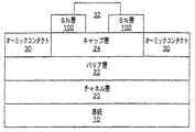
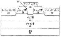
図1A及び図1Bは、本発明に係るIII族窒化物高電子移動度トランジスタの一実施形態を説明するための断面概略図で、キャップ層24、24’を有するIII族窒化物高電子移動度トランジスタを示す図である。
Claims (111)
- III族窒化物ベースのチャネル層と、
該チャネル層上に設けられたIII族窒化物ベースのバリア層と、
該バリア層上に設けられた不均一組成AlGaNベースのキャップ層とを備え、
該キャップ層が、前記バリア層から遠い方の前記キャップ層の表面付近に、前記AlGaNベースのキャップ層内の領域に存在するよりも高い濃度のAlを有することを特徴とするIII族窒化物高電子移動度トランジスタ。 - 前記AlGaNベースのキャップ層の中へ入り込んでいるゲートコンタクトをさらに備え、前記高濃度のAlが前記キャップ層の中へ約30Åから約1000Åまで延在することを特徴とする請求項1に記載のIII族窒化物高電子移動度トランジスタ。
- 前記AlGaNベースのキャップ層の中へ入り込んでいないゲートコンタクトを前記AlGaNベースのキャップ層上にさらに備え、前記高濃度のAlが前記キャップ層の中へ約2.5Åから約100Åまで延在することを特徴とする請求項1に記載のIII族窒化物高電子移動度トランジスタ。
- 前記AlGaNベースのキャップ層は、前記バリア層から遠い方の前記キャップ層の前記表面付近にAlxGa1-xN(ただしx≦1)からなる第1の領域と、前記AlGaNベースのキャップ層内にAlyGa1-yN(ただしy<1、y<x)からなる第2の領域とを含むことを特徴とする請求項1に記載のIII族窒化物高電子移動度トランジスタ。
- xは約0.3から約1、yは約0.2から約0.9であることを特徴とする請求項4に記載のIII族窒化物高電子移動度トランジスタ。
- 前記AlGaNベースのキャップ層は、前記バリア層と前記AlGaNベースのキャップ層との間の境界面にAlzGa1-zN(ただし、z<1、z≠y)からなる第3の領域をさらに含むことを特徴とする請求項4に記載のIII族窒化物高電子移動度トランジスタ。
- z>yであることを特徴とする請求項6に記載のIII族窒化物高電子移動度トランジスタ。
- z>xであることを特徴とする請求項7に記載のIII族窒化物高電子移動度トランジスタ。
- z≦xであることを特徴とする請求項6に記載のIII族窒化物高電子移動度トランジスタ。
- 前記チャネル層はGaN層を備え、前記バリア層はAlGaN層を備え、前記キャップ層はAlGaN層を備えることを特徴とする請求項1に記載のIII族窒化物高電子移動度トランジスタ。
- III族窒化物ベースのチャネル層と、
該チャネル層上に設けられたIII族窒化物ベースのバリア層と、
該バリア層上に設けられたIII族窒化物ベースのキャップ層とを備え、
前記キャップ層が、前記バリア層から遠い方の前記キャップ層の表面付近にドープ領域を有することを特徴とするIII族窒化物高電子移動度トランジスタ。 - 前記ドープ領域は、n型ドーパントでドープされた領域を含むことを特徴とする請求項11に記載のIII族窒化物高電子移動度トランジスタ。
- 前記n型ドーパントは、Si、Ge、及び/又はOを含むことを特徴とする請求項12に記載のIII族窒化物高電子移動度トランジスタ。
- 前記キャップ層の中へ入り込んでいないゲートコンタクトを前記キャップ層上にさらに備え、前記ドープ領域が前記キャップ層の中へ約2.5Åから約50Åまで延在することを特徴とする請求項12に記載のIII族窒化物高電子移動度トランジスタ。
- 前記キャップ層の中へ入り込んでいるゲートコンタクトをさらに備え、前記ドープ領域が前記キャップ層の中へ約20Åから約5000Åまで延在することを特徴とする請求項12に記載のIII族窒化物高電子移動度トランジスタ。
- 前記ドープ領域は、約1018から約1021cm-3のドーパント濃度をもたらすことを特徴とする請求項12に記載のIII族窒化物高電子移動度トランジスタ。
- 前記ドープ領域は、前記キャップ層の前記表面又は前記表面近くに1つ又は複数のデルタドープ領域を含むことを特徴とする請求項12に記載のIII族窒化物高電子移動度トランジスタ。
- 前記1つ又は複数のデルタドープ領域は、約1011から約1015cm-2のドーパント濃度を有することを特徴とする請求項17に記載のIII族窒化物高電子移動度トランジスタ。
- 前記n型ドーパントはOを含み、前記ドープ領域は、前記キャップ層の中へ約20Å延在することを特徴とする請求項12に記載のIII族窒化物高電子移動度トランジスタ。
- 前記ドープ領域は、p型ドーパントでドープされた領域を含むことを特徴とする請求項11に記載のIII族窒化物高電子移動度トランジスタ。
- 前記キャップ層の中へ入り込んでいないゲートコンタクトを前記キャップ層上にさらに備え、前記ドープ領域は、前記キャップ層の中へ約2.5Åから約50Åまで延在することを特徴とする請求項20に記載のIII族窒化物高電子移動度トランジスタ。
- 前記キャップ層の中へ入り込んでいるゲートコンタクトをさらに備え、前記ドープ領域は、前記キャップ層の中へ約30Åから約5000Åまで延在することを特徴とする請求項20に記載のIII族窒化物高電子移動度トランジスタ。
- 前記p型ドーパントは、約1016から約1022cm-3のドーパント濃度を与えることを特徴とする請求項20に記載のIII族窒化物高電子移動度トランジスタ。
- 前記p型ドーパントは、Mg、Be、Zn、Ca、及び/又はCを含むことを特徴とする請求項20に記載のIII族窒化物高電子移動度トランジスタ。
- 前記ドープ領域は、1つ又は複数のデルタドープ領域を前記キャップ層の前記表面又は前記表面近くに含むことを特徴とする請求項20に記載のIII族窒化物高電子移動度トランジスタ。
- 前記デルタドープ領域は、約1011から約1015cm-2のドーパント濃度を有することを特徴とする請求項25に記載のIII族窒化物高電子移動度トランジスタ。
- 前記キャップ層内に設けられた凹部と、
該凹部内に、前記キャップ層と直接に接触していないゲートコンタクトとをさらに備え、前記p型ドーパントのレベルは、前記キャップ層内に伝導領域をもたらすことを特徴とする請求項20に記載のIII族窒化物高電子移動度トランジスタ。 - 前記凹部の側壁上に絶縁層をさらに備え、前記ゲートコンタクトは、前記凹部内の前記絶縁層上にあることを特徴とする請求項20に記載のIII族窒化物高電子移動度トランジスタ。
- 前記ドープ領域は、前記キャップ層とp−n接合を形成し、前記ゲートコンタクトは、前記ドープ領域の直上にあることを特徴とする請求項20に記載のIII族窒化物高電子移動度トランジスタ。
- 前記ドープ領域は、深いレベルのドーパントでドープした領域を含むことを特徴とする請求項11に記載のIII族窒化物高電子移動度トランジスタ。
- 前記キャップ層の中へ入り込んでいないゲートコンタクトを前記キャップ層上にさらに備え、前記ドープ領域は、前記キャップ層の中へ約2.5Åから約100Åまで延在することを特徴とする請求項30に記載のIII族窒化物高電子移動度トランジスタ。
- 前記キャップ層の中へ入り込んでいるゲートコンタクトをさらに備え、前記ドープ領域は、前記キャップ層の中へ約30Åから約5000Åまで延在することを特徴とする請求項30に記載のIII族窒化物高電子移動度トランジスタ。
- 前記深いレベルのドーパントは、約1016から約1022cm-3のドーパント濃度を与えることを特徴とする請求項30に記載のIII族窒化物高電子移動度トランジスタ。
- 前記深いレベルのドーパントは、Fe、C、V、Cr、Mn、Ni、Co及び/又は他の希土類元素を含むことを特徴とする請求項30に記載のIII族窒化物高電子移動度トランジスタ。
- 前記ドープ領域は第1のドープ領域を含み、前記キャップ層は、前記バリア層と前記第1のドープ領域の間に第2のドープ領域をさらに含み、前記第2のドープ領域のドーパント濃度は、前記第1のドープ領域のドーパント濃度よりも少ないことを特徴とする請求項11に記載のIII族窒化物高電子移動度トランジスタ。
- 前記第2のドープ領域は、前記キャップ層の、前記第1のドープ領域内ではない残りの部分を含むことを特徴とする請求項35に記載のIII族窒化物高電子移動度トランジスタ。
- 前記キャップ層は、n型ドーパントとp型ドーパント及び深いレベルのドーパントのうち少なくとも2つでドープされることを特徴とする請求項11に記載のIII族窒化物高電子移動度トランジスタ。
- 前記チャネル層はGaN層を含み、前記バリア層はAlGaN層を含み、前記キャップ層はGaN層又はAlGaN層を含むことを特徴とする請求項11に記載のIII族窒化物高電子移動度トランジスタ。
- III族窒化物ベースのチャネル層を形成するステップと、
該チャネル層上にIII族窒化物ベースのバリア層を形成するステップと、
該バリア層上に不均一組成AlGaNベースのキャップ層を形成するステップとを含み、
前記キャップ層が、前記バリア層から遠い方の前記キャップ層の表面に、前記AlGaNベースのキャップ層内の領域に存在するよりも高い濃度のAlを有することを特徴とするIII族窒化物高電子移動度トランジスタの製造方法。 - 前記不均一組成AlGaNベースのキャップ層を形成するステップは、
前記キャップ層の前記表面付近にAlxGa1-xN(ただしx≦1)からなる第1の領域形成するステップと、
前記AlGaNベースのキャップ層内にAlyGa1-yN(ただしy<1、y<x)からなる第2の領域を形成するステップとを含むことを特徴とする請求項39に記載のIII族窒化物高電子移動度トランジスタの製造方法。 - III族窒化物ベースのチャネル層を形成するステップと、
該チャネル層上にIII族窒化物ベースのバリア層を形成するステップと、
該バリア層上にIII族窒化物ベースのキャップ層を形成するステップとを含み、
該キャップ層が、前記バリア層から遠い方の前記キャップ層の表面付近にドープ領域を有することを特徴とするIII族窒化物高電子移動度トランジスタの製造方法。 - 前記ドープ領域は、n型ドーパントとp型ドーパント及び/又は深いレベルのドーパントでドープされることを特徴とする請求項41に記載のIII族窒化物高電子移動度トランジスタの製造方法。
- 広バンドギャップ半導体材料からなる領域の表面の少なくとも一部分上に、黒鉛状及び/又は非晶質BN層を形成するステップを含むことを特徴とする広バンドギャップ半導体デバイスの表面を不活性化するIII族窒化物高電子移動度トランジスタの製造方法。
- 前記広バンドギャップ半導体デバイスは、III族窒化物半導体デバイスを含むことを特徴とする請求項43に記載のIII族窒化物高電子移動度トランジスタの製造方法。
- 前記広バンドギャップ半導体デバイスは、GaNベースの半導体デバイスを含むことを特徴とする請求項43に記載のIII族窒化物高電子移動度トランジスタの製造方法。
- 前記広バンドギャップ半導体デバイスは、III族窒化物高電子移動度トランジスタを含むことを特徴とする請求項43に記載のIII族窒化物高電子移動度トランジスタの製造方法。
- 前記黒鉛状及び/又は非晶質BN層を形成するステップは、前記広バンドギャップ半導体デバイス中の広バンドギャップ半導体材料の分解温度未満の温度で実施されることを特徴とする請求項43に記載のIII族窒化物高電子移動度トランジスタの製造方法。
- 前記黒鉛状及び/又は非晶質BN層を形成するステップは、約1100℃未満の温度で実施されることを特徴とする請求項43に記載のIII族窒化物高電子移動度トランジスタの製造方法。
- 前記黒鉛状及び/又は非晶質BN層を形成するステップは、約1000℃未満の温度で実施されることを特徴とする請求項43に記載のIII族窒化物高電子移動度トランジスタの製造方法。
- 前記黒鉛状及び/又は非晶質BN層を形成するステップは、約900℃未満の温度で実施されることを特徴とする請求項43に記載のIII族窒化物高電子移動度トランジスタの製造方法。
- 前記BN層は、非単結晶になるように形成されることを特徴とする請求項43に記載のIII族窒化物高電子移動度トランジスタの製造方法。
- 前記黒鉛状及び/又は非晶質BN層は、約3Åから約1μmの厚さに形成されることを特徴とする請求項43に記載のIII族窒化物高電子移動度トランジスタの製造方法。
- 前記黒鉛状及び/又は非晶質BN層を形成するステップは、キャリアガスと共にTEB及びNH3を流すステップを含むことを特徴とする請求項43に記載のIII族窒化物高電子移動度トランジスタの製造方法。
- 広バンドギャップ半導体材料からなる領域の表面の少なくとも一部分上に、黒鉛状及び/又は非晶質BNの層を含むことを特徴とする広バンドギャップ半導体デバイスの不活性構造体。
- 前記広バンドギャップ半導体デバイスは、III族窒化物半導体デバイスを含むことを特徴とする請求項54に記載の不活性構造体。
- III族窒化物半導体材料からなる領域の表面の少なくとも一部分上にSiC層を形成するステップを含むことを特徴とするIII族窒化物半導体デバイスの表面不活性化方法。
- 前記III族窒化物半導体デバイスは、GaNベースの半導体デバイスを含むことを特徴とする請求項56の表面不活性化方法。
- 前記III族窒化物半導体デバイスは、III族窒化物高電子移動度トランジスタを含むことを特徴とする請求項56に記載の表面不活性化方法。
- 前記SiC層を形成するステップは、前記III族窒化物半導体デバイス中のIII族窒化物半導体材料の分解温度未満の温度で実施されることを特徴とする請求項56に記載の表面不活性化方法。
- 前記SiC層を形成するステップは、約1100℃未満の温度で実施されることを特徴とする請求項56に記載の表面不活性化方法。
- 前記SiC層を形成するステップは、約1000℃未満の温度で実施されることを特徴とする請求項56に記載の表面不活性化方法。
- 前記SiC層を形成するステップは、約900℃未満の温度で実施されることを特徴とする請求項56に記載の表面不活性化方法。
- 前記SiC層は、非単結晶になるように形成されることを特徴とする請求項56に記載の表面不活性化方法。
- 前記SiC層を形成するステップは、3C SiC層を形成するステップを含むことを特徴とする請求項56に記載の表面不活性化方法。
- 前記SiC層は、約3Åから約1μmの厚さに形成されることを特徴とする請求項56に記載の表面不活性化方法。
- 前記SiC層は、p型SiCであることを特徴とする請求項56に記載の表面不活性化方法。
- 前記SiC層は、絶縁SiCであることを特徴とする請求項56に記載の表面不活性化方法。
- III族窒化物半導体材料からなる領域の表面の少なくとも一部分上にSiCの層を含むことを特徴とするIII族窒化物半導体デバイスの不活性構造体。
- 前記III族窒化物半導体デバイスは、GaNベースの半導体デバイスを含むことを特徴とする請求項68に記載の不活性構造体。
- 前記SiC層は、p型SiCであることを特徴とする請求項68に記載の不活性構造体。
- 前記SiC層は、絶縁SiCであることを特徴とする請求項68に記載の不活性構造体。
- III族窒化物半導体材料からなる領域の表面の少なくとも一部分上に直接に不活性層を形成するステップと、
前記不活性層を酸素含有環境中でアニールするステップとを含むことを特徴とするIII族窒化物半導体デバイスの不活性構造体の製造方法。 - 前記不活性層は、SiN及び/又はMgNを含むことを特徴とする請求項72に記載のIII族窒化物半導体デバイスの不活性構造体の製造方法。
- 前記不活性層は、BN及び/又はSiCを含むことを特徴とする請求項72に記載のIII族窒化物半導体デバイスの不活性構造体の製造方法。
- 前記不活性層は、SiO2、MgO、Al2O3、Sc2O3、及び/又はAlNを含むことを特徴とする請求項72に記載のIII族窒化物半導体デバイスの不活性構造体の製造方法。
- 前記アニールするステップは、約100℃から約1100℃の温度で、約10秒から約1時間の間実施されることを特徴とする請求項72に記載のIII族窒化物半導体デバイスの不活性構造体の製造方法。
- 前記酸素含有環境は、O2、O3、CO2、CO、N2O、D2O、及び/又はNOを含むことを特徴とする請求項72に記載のIII族窒化物半導体デバイスの不活性構造体の製造方法。
- 前記アニールするステップは、前記不活性層の下の構造体を酸化するには不十分であるが前記不活性層から少なくとも一部の水素を除去するには十分なある温度及び時間で実施されることを特徴とする請求項72に記載のIII族窒化物半導体デバイスの不活性構造体の製造方法。
- 前記III族窒化物半導体材料は、GaNベースの材料を含むことを特徴とする請求項72に記載のIII族窒化物半導体デバイスの不活性構造体の製造方法。
- III族窒化物半導体材料からなる領域の表面の少なくとも一部分上に直接に不活性層を形成するステップと、
前記不活性層をD2及び/又はD2O中でアニールするステップとを含むことを特徴とするIII族窒化物半導体デバイスの不活性構造体の製造方法。 - 前記不活性層は、SiN及び/又はMgNを含むことを特徴とする請求項80に記載のIII族窒化物半導体デバイスの不活性構造体の製造方法。
- 前記不活性層は、BN及び/又はSiCを含むことを特徴とする請求項80に記載のIII族窒化物半導体デバイスの不活性構造体の製造方法。
- 前記不活性層は、SiO2、MgO、Al2O3、Sc2O3、及び/又はAlNを含むことを特徴とする請求項80に記載のIII族窒化物半導体デバイスの不活性構造体の製造方法。
- 前記アニールするステップは、前記不活性層の下の構造体を酸化するには不十分であるが前記不活性層から少なくとも一部の水素を除去するには十分な、あるいは前記不活性層中の少なくとも一部の水素を重水素で置換するには十分なある温度及び時間で実施されることを特徴とする請求項80に記載のIII族窒化物半導体デバイスの不活性構造体の製造方法。
- 前記III族窒化物半導体材料は、GaNベースの材料を含むことを特徴とする請求項80に記載のIII族窒化物半導体デバイスの不活性構造体の製造方法。
- III族窒化物ベースのチャネル層と、
該チャネル層上に設けられたIII族窒化物ベースのバリア層と、
該バリア層上に設けられたAlNキャップ層と
を備えることを特徴とするIII族窒化物高電子移動度トランジスタ。 - 前記AlNキャップ層の中へ入り込んでいるゲートコンタクトをさらに備え、前記AlNキャップ層は、約10Åから約5000Åの厚さを有することを特徴とする請求項86に記載のIII族窒化物高電子移動度トランジスタ。
- 前記AlNキャップ層の中へ入り込んでいないゲートコンタクトを前記AlNキャップ層上にさらに備え、前記AlNキャップ層は、約2Åから約50Åの厚さを有することを特徴とする請求項86に記載のIII族窒化物高電子移動度トランジスタ。
- 前記チャネル層はGaN層を含み、前記バリア層はAlGaN層を含むことを特徴とする請求項86に記載のIII族窒化物高電子移動度トランジスタ。
- 前記AlNキャップ層と前記バリア層の間に配置された少なくとも1つのIII族窒化物層をさらに備えることを特徴とする請求項86に記載のIII族窒化物高電子移動度トランジスタ。
- 前記AlNキャップ層は、非単結晶であることを特徴とする請求項86に記載のIII族窒化物高電子移動度トランジスタ。
- 前記AlNキャップ層の結晶構造は、前記AlNキャップ層がその上に形成される層の結晶構造とコヒーレントではないことを特徴とする請求項86に記載のIII族窒化物高電子移動度トランジスタ。
- III族窒化物ベースのチャネル層を形成するステップと、
該チャネル層上にIII族窒化物ベースのバリア層を形成するステップと、
該バリア層上にAlNキャップ層を形成するステップと
を含むことを特徴とするIII族窒化物高電子移動度トランジスタの製造方法。 - III族窒化物ベースのチャネル層と、
該チャネル層上に設けられたIII族窒化物ベースのバリア層と、
該バリア層上に設けられた保護層と、
該バリア層上に設けられたゲートコンタクトと、
前記保護層上に設けられたオーミックコンタクトと
を備えることを特徴とするIII族窒化物高電子移動度トランジスタ。 - 前記保護層は、SiNを含むことを特徴とする請求項94に記載のIII族窒化物高電子移動度トランジスタ。
- 前記保護層は、BNを含むことを特徴とする請求項94に記載のIII族窒化物高電子移動度トランジスタ。
- 前記保護層は、MgNを含むことを特徴とする請求項94に記載のIII族窒化物高電子移動度トランジスタ。
- 前記保護層は、SiO2、MgO、Al2O3、Sc2O3、及び/又はAlNを含むことを特徴とする請求項94に記載のIII族窒化物高電子移動度トランジスタ。
- 前記保護層は、約1単分子層の厚さを有することを特徴とする請求項94に記載のIII族窒化物高電子移動度トランジスタ。
- 前記保護層は、多層を含むことを特徴とする請求項94に記載のIII族窒化物高電子移動度トランジスタ。
- 前記多層は、SiNの層及びAlNの層を含むことを特徴とする請求項100に記載のIII族窒化物高電子移動度トランジスタ。
- 前記保護層は、約1Åから約10Åの厚さを有することを特徴とする請求項94に記載のIII族窒化物高電子移動度トランジスタ。
- 前記ゲートコンタクトは、前記保護層上にあることを特徴とする請求項94に記載のIII族窒化物高電子移動度トランジスタ。
- 前記オーミックコンタクトは、前記保護層の直上にあることを特徴とする請求項94に記載のIII族窒化物高電子移動度トランジスタ。
- III族窒化物ベースのチャネル層を形成するステップと、
該チャネル層上にIII族窒化物ベースのバリア層を形成するステップと、
該バリア層上に保護層を形成するステップと、
前記バリア層上にゲートコンタクトを形成するステップと、
前記保護層上にオーミックコンタクトを形成するステップと
を含むことを特徴とするIII族窒化物高電子移動度トランジスタの製造方法。 - 前記保護層を形成するステップは、前記バリア層を形成する前記ステップと共に本来の場所で実施されることを特徴とする請求項105に記載のIII族窒化物高電子移動度トランジスタの製造方法。
- 前記保護層を形成するステップは、SiN、BN、及び/又はMgNを含む層を形成するステップを含むことを特徴とする請求項105に記載のIII族窒化物高電子移動度トランジスタの製造方法。
- 前記保護層は、約1単分子層の厚さに形成されることを特徴とする請求項105に記載のIII族窒化物高電子移動度トランジスタの製造方法。
- 前記保護層を形成するステップは、多層を形成するステップを含むことを特徴とする請求項105に記載のIII族窒化物高電子移動度トランジスタの製造方法。
- 前記多層を形成するステップは、SiNの層を形成するステップと、AlNの層を形成するステップとを含むことを特徴とする請求項109に記載のIII族窒化物高電子移動度トランジスタの製造方法。
- 前記保護層は、約1Åから約10Åの厚さに形成されることを特徴とする請求項105に記載のIII族窒化物高電子移動度トランジスタの製造方法。
Applications Claiming Priority (3)
| Application Number | Priority Date | Filing Date | Title |
|---|---|---|---|
| US10/996,249 US7456443B2 (en) | 2004-11-23 | 2004-11-23 | Transistors having buried n-type and p-type regions beneath the source region |
| US10/996,249 | 2004-11-23 | ||
| PCT/US2005/031272 WO2006057686A2 (en) | 2004-11-23 | 2005-08-31 | Cap layers and/or passivation layers for nitride-based transistors, transistor structures and methods of fabricating same |
Publications (3)
| Publication Number | Publication Date |
|---|---|
| JP2008521248A true JP2008521248A (ja) | 2008-06-19 |
| JP2008521248A5 JP2008521248A5 (ja) | 2008-07-31 |
| JP5406452B2 JP5406452B2 (ja) | 2014-02-05 |
Family
ID=35457428
Family Applications (1)
| Application Number | Title | Priority Date | Filing Date |
|---|---|---|---|
| JP2007543022A Active JP5406452B2 (ja) | 2004-11-23 | 2005-08-31 | 窒化物ベースのトランジスタ及びトランジスタ構造体のキャップ層及び/又は不活性層並びにそれらの製造方法 |
Country Status (8)
| Country | Link |
|---|---|
| US (2) | US7456443B2 (ja) |
| EP (1) | EP1817798B2 (ja) |
| JP (1) | JP5406452B2 (ja) |
| KR (1) | KR101124937B1 (ja) |
| CN (1) | CN101107713A (ja) |
| CA (1) | CA2588114A1 (ja) |
| TW (1) | TWI464876B (ja) |
| WO (1) | WO2006057686A2 (ja) |
Cited By (5)
| Publication number | Priority date | Publication date | Assignee | Title |
|---|---|---|---|---|
| JP2006165314A (ja) * | 2004-12-08 | 2006-06-22 | New Japan Radio Co Ltd | 窒化物半導体装置及びその製造方法 |
| JP2016524817A (ja) * | 2013-06-06 | 2016-08-18 | 蘇州晶湛半導体有限公司Enkris Semiconductor,Inc. | 半導体デバイスおよびその製作方法 |
| WO2020067215A1 (ja) * | 2018-09-28 | 2020-04-02 | Dowaエレクトロニクス株式会社 | Iii族窒化物半導体発光素子およびその製造方法 |
| JP2020524399A (ja) * | 2017-06-19 | 2020-08-13 | エピガン ナムローゼ フェンノートシャップ | 高電子移動度トランジスタ |
| US11476358B2 (en) | 2020-08-06 | 2022-10-18 | Kabushiki Kaisha Toshiba | Semiconductor device |
Families Citing this family (148)
| Publication number | Priority date | Publication date | Assignee | Title |
|---|---|---|---|---|
| US7501669B2 (en) | 2003-09-09 | 2009-03-10 | Cree, Inc. | Wide bandgap transistor devices with field plates |
| US7612390B2 (en) | 2004-02-05 | 2009-11-03 | Cree, Inc. | Heterojunction transistors including energy barriers |
| US9773877B2 (en) | 2004-05-13 | 2017-09-26 | Cree, Inc. | Wide bandgap field effect transistors with source connected field plates |
| US7417266B1 (en) | 2004-06-10 | 2008-08-26 | Qspeed Semiconductor Inc. | MOSFET having a JFET embedded as a body diode |
| EP2273553B1 (en) * | 2004-06-30 | 2020-02-12 | IMEC vzw | A method for fabricating AlGaN/GaN HEMT devices |
| US7456443B2 (en) | 2004-11-23 | 2008-11-25 | Cree, Inc. | Transistors having buried n-type and p-type regions beneath the source region |
| KR100597649B1 (ko) * | 2004-11-26 | 2006-07-05 | 삼성전자주식회사 | 베리어 메탈을 포함하는 반도체 디바이스의 제조방법 및그 구조 |
| US9640649B2 (en) * | 2004-12-30 | 2017-05-02 | Infineon Technologies Americas Corp. | III-nitride power semiconductor with a field relaxation feature |
| US7436039B2 (en) * | 2005-01-06 | 2008-10-14 | Velox Semiconductor Corporation | Gallium nitride semiconductor device |
| US11791385B2 (en) | 2005-03-11 | 2023-10-17 | Wolfspeed, Inc. | Wide bandgap transistors with gate-source field plates |
| US9331192B2 (en) * | 2005-06-29 | 2016-05-03 | Cree, Inc. | Low dislocation density group III nitride layers on silicon carbide substrates and methods of making the same |
| US20070018198A1 (en) * | 2005-07-20 | 2007-01-25 | Brandes George R | High electron mobility electronic device structures comprising native substrates and methods for making the same |
| JP2007048783A (ja) * | 2005-08-05 | 2007-02-22 | Matsushita Electric Ind Co Ltd | ショットキーダイオード及びその製造方法 |
| JP4751150B2 (ja) * | 2005-08-31 | 2011-08-17 | 株式会社東芝 | 窒化物系半導体装置 |
| JP2007095858A (ja) * | 2005-09-28 | 2007-04-12 | Toshiba Ceramics Co Ltd | 化合物半導体デバイス用基板およびそれを用いた化合物半導体デバイス |
| US8026568B2 (en) | 2005-11-15 | 2011-09-27 | Velox Semiconductor Corporation | Second Schottky contact metal layer to improve GaN Schottky diode performance |
| US7932539B2 (en) * | 2005-11-29 | 2011-04-26 | The Hong Kong University Of Science And Technology | Enhancement-mode III-N devices, circuits, and methods |
| US7972915B2 (en) * | 2005-11-29 | 2011-07-05 | The Hong Kong University Of Science And Technology | Monolithic integration of enhancement- and depletion-mode AlGaN/GaN HFETs |
| US8044432B2 (en) * | 2005-11-29 | 2011-10-25 | The Hong Kong University Of Science And Technology | Low density drain HEMTs |
| US7338826B2 (en) * | 2005-12-09 | 2008-03-04 | The United States Of America As Represented By The Secretary Of The Navy | Silicon nitride passivation with ammonia plasma pretreatment for improving reliability of AlGaN/GaN HEMTs |
| JP4705482B2 (ja) * | 2006-01-27 | 2011-06-22 | パナソニック株式会社 | トランジスタ |
| US7388236B2 (en) * | 2006-03-29 | 2008-06-17 | Cree, Inc. | High efficiency and/or high power density wide bandgap transistors |
| JP2007329350A (ja) * | 2006-06-08 | 2007-12-20 | Matsushita Electric Ind Co Ltd | 半導体装置 |
| US20080067549A1 (en) * | 2006-06-26 | 2008-03-20 | Armin Dadgar | Semiconductor component |
| US7504309B2 (en) * | 2006-10-12 | 2009-03-17 | International Business Machines Corporation | Pre-silicide spacer removal |
| US7393746B2 (en) | 2006-10-12 | 2008-07-01 | International Business Machines Corporation | Post-silicide spacer removal |
| JP4282708B2 (ja) * | 2006-10-20 | 2009-06-24 | 株式会社東芝 | 窒化物系半導体装置 |
| US8823057B2 (en) | 2006-11-06 | 2014-09-02 | Cree, Inc. | Semiconductor devices including implanted regions for providing low-resistance contact to buried layers and related devices |
| JP4296195B2 (ja) * | 2006-11-15 | 2009-07-15 | シャープ株式会社 | 電界効果トランジスタ |
| JP2008124374A (ja) * | 2006-11-15 | 2008-05-29 | Sharp Corp | 絶縁ゲート電界効果トランジスタ |
| US7692263B2 (en) | 2006-11-21 | 2010-04-06 | Cree, Inc. | High voltage GaN transistors |
| US8878245B2 (en) * | 2006-11-30 | 2014-11-04 | Cree, Inc. | Transistors and method for making ohmic contact to transistors |
| JP5260550B2 (ja) * | 2007-01-10 | 2013-08-14 | インターナショナル レクティフィアー コーポレイション | Iii族窒化物素子のための活性領域成形およびその製造方法 |
| US7939853B2 (en) * | 2007-03-20 | 2011-05-10 | Power Integrations, Inc. | Termination and contact structures for a high voltage GaN-based heterojunction transistor |
| US20090321787A1 (en) * | 2007-03-20 | 2009-12-31 | Velox Semiconductor Corporation | High voltage GaN-based heterojunction transistor structure and method of forming same |
| US9484499B2 (en) * | 2007-04-20 | 2016-11-01 | Cree, Inc. | Transparent ohmic contacts on light emitting diodes with carrier substrates |
| US9209281B2 (en) * | 2007-04-23 | 2015-12-08 | Infineon Technologies Ag | Method of manufacturing a device by locally heating one or more metallization layers and by means of selective etching |
| CN101359686B (zh) * | 2007-08-03 | 2013-01-02 | 香港科技大学 | 可靠的常关型ⅲ-氮化物有源器件结构及相关方法和系统 |
| JP5285252B2 (ja) * | 2007-09-12 | 2013-09-11 | 新日本無線株式会社 | 窒化物半導体装置 |
| JP4462330B2 (ja) * | 2007-11-02 | 2010-05-12 | 住友電気工業株式会社 | Iii族窒化物電子デバイス |
| US8368100B2 (en) | 2007-11-14 | 2013-02-05 | Cree, Inc. | Semiconductor light emitting diodes having reflective structures and methods of fabricating same |
| EP2071509A1 (en) * | 2007-12-13 | 2009-06-17 | Gemalto SA | Method and apparatus to mark a document using a combination between guilloches and watermarking, method and apparatus to read previous combination |
| US8076699B2 (en) * | 2008-04-02 | 2011-12-13 | The Hong Kong Univ. Of Science And Technology | Integrated HEMT and lateral field-effect rectifier combinations, methods, and systems |
| US8519438B2 (en) | 2008-04-23 | 2013-08-27 | Transphorm Inc. | Enhancement mode III-N HEMTs |
| US8289065B2 (en) | 2008-09-23 | 2012-10-16 | Transphorm Inc. | Inductive load power switching circuits |
| US20100084687A1 (en) * | 2008-10-03 | 2010-04-08 | The Hong Kong University Of Science And Technology | Aluminum gallium nitride/gallium nitride high electron mobility transistors |
| US7898004B2 (en) | 2008-12-10 | 2011-03-01 | Transphorm Inc. | Semiconductor heterostructure diodes |
| US8080820B2 (en) * | 2009-03-16 | 2011-12-20 | Intel Corporation | Apparatus and methods for improving parallel conduction in a quantum well device |
| KR101694883B1 (ko) * | 2009-04-08 | 2017-01-10 | 이피션트 파워 컨버젼 코퍼레이션 | 역확산 억제 구조 |
| JP5785153B2 (ja) * | 2009-04-08 | 2015-09-24 | エフィシエント パワー コンヴァーション コーポレーション | 補償型ゲートmisfet及びその製造方法 |
| US8741715B2 (en) | 2009-04-29 | 2014-06-03 | Cree, Inc. | Gate electrodes for millimeter-wave operation and methods of fabrication |
| US8742459B2 (en) | 2009-05-14 | 2014-06-03 | Transphorm Inc. | High voltage III-nitride semiconductor devices |
| KR101649004B1 (ko) * | 2009-05-26 | 2016-08-17 | 스미또모 가가꾸 가부시키가이샤 | 반도체 기판, 반도체 기판의 제조 방법 및 전자 디바이스 |
| US9306050B2 (en) * | 2009-06-26 | 2016-04-05 | Cornell University | III-V semiconductor structures including aluminum-silicon nitride passivation |
| JP4700125B2 (ja) | 2009-07-30 | 2011-06-15 | 住友電気工業株式会社 | 半導体装置およびその製造方法 |
| US8390000B2 (en) | 2009-08-28 | 2013-03-05 | Transphorm Inc. | Semiconductor devices with field plates |
| US8389977B2 (en) | 2009-12-10 | 2013-03-05 | Transphorm Inc. | Reverse side engineered III-nitride devices |
| US8936976B2 (en) * | 2009-12-23 | 2015-01-20 | Intel Corporation | Conductivity improvements for III-V semiconductor devices |
| KR101774933B1 (ko) * | 2010-03-02 | 2017-09-06 | 삼성전자 주식회사 | 듀얼 디플리션을 나타내는 고 전자 이동도 트랜지스터 및 그 제조방법 |
| JP5604147B2 (ja) * | 2010-03-25 | 2014-10-08 | パナソニック株式会社 | トランジスタ及びその製造方法 |
| US8809904B2 (en) | 2010-07-26 | 2014-08-19 | Cree, Inc. | Electronic device structure with a semiconductor ledge layer for surface passivation |
| JPWO2012014675A1 (ja) * | 2010-07-29 | 2013-09-12 | 日本碍子株式会社 | 半導体素子、hemt素子、および半導体素子の製造方法 |
| CN103003931B (zh) * | 2010-07-29 | 2016-01-13 | 日本碍子株式会社 | 半导体元件用外延基板、半导体元件、pn接合二极管元件以及半导体元件用外延基板的制造方法 |
| US8742460B2 (en) | 2010-12-15 | 2014-06-03 | Transphorm Inc. | Transistors with isolation regions |
| US8643062B2 (en) | 2011-02-02 | 2014-02-04 | Transphorm Inc. | III-N device structures and methods |
| US8716141B2 (en) | 2011-03-04 | 2014-05-06 | Transphorm Inc. | Electrode configurations for semiconductor devices |
| US8772842B2 (en) | 2011-03-04 | 2014-07-08 | Transphorm, Inc. | Semiconductor diodes with low reverse bias currents |
| FR2974242B1 (fr) * | 2011-04-14 | 2013-09-27 | Thales Sa | Amelioration des proprietes de transport dans les transistors hemts composes de semi-conducteurs bores a larges bande interdite (iii-b)-n |
| KR20120124101A (ko) * | 2011-05-03 | 2012-11-13 | 삼성전자주식회사 | 고효율 질화계 이종접합 전계효과 트랜지스터 |
| KR101813177B1 (ko) | 2011-05-06 | 2017-12-29 | 삼성전자주식회사 | 고전자이동도 트랜지스터 및 그 제조방법 |
| KR20130008280A (ko) * | 2011-07-12 | 2013-01-22 | 삼성전자주식회사 | 안정성이 우수한 질화물계 반도체 소자 |
| KR101259126B1 (ko) * | 2011-07-25 | 2013-04-26 | 엘지전자 주식회사 | 질화물계 반도체 이종접합 반도체 소자 및 그 제조방법 |
| KR20130014861A (ko) * | 2011-08-01 | 2013-02-12 | 삼성전자주식회사 | 고 전자 이동도 트랜지스터 및 그 제조방법 |
| US8901604B2 (en) | 2011-09-06 | 2014-12-02 | Transphorm Inc. | Semiconductor devices with guard rings |
| US9257547B2 (en) | 2011-09-13 | 2016-02-09 | Transphorm Inc. | III-N device structures having a non-insulating substrate |
| JP5739774B2 (ja) * | 2011-09-13 | 2015-06-24 | トランスフォーム・ジャパン株式会社 | 化合物半導体装置及びその製造方法 |
| JP5896667B2 (ja) * | 2011-09-26 | 2016-03-30 | トランスフォーム・ジャパン株式会社 | 化合物半導体装置及びその製造方法 |
| JP5784440B2 (ja) * | 2011-09-28 | 2015-09-24 | トランスフォーム・ジャパン株式会社 | 半導体装置の製造方法及び半導体装置 |
| US8598937B2 (en) | 2011-10-07 | 2013-12-03 | Transphorm Inc. | High power semiconductor electronic components with increased reliability |
| CN102509569B (zh) * | 2011-10-19 | 2014-04-16 | 西安电子科技大学 | I层钒掺杂的碳化硅肖特基结型核电池及其制作方法 |
| US9472633B1 (en) * | 2011-11-28 | 2016-10-18 | Qorvo Us, Inc. | Transistor gate having an insulating layer support structure |
| US8633094B2 (en) | 2011-12-01 | 2014-01-21 | Power Integrations, Inc. | GaN high voltage HFET with passivation plus gate dielectric multilayer structure |
| US8530978B1 (en) | 2011-12-06 | 2013-09-10 | Hrl Laboratories, Llc | High current high voltage GaN field effect transistors and method of fabricating same |
| US8940620B2 (en) | 2011-12-15 | 2015-01-27 | Power Integrations, Inc. | Composite wafer for fabrication of semiconductor devices |
| US9337301B2 (en) | 2011-12-21 | 2016-05-10 | Massachusetts Institute Of Technology | Aluminum nitride based semiconductor devices |
| US9165766B2 (en) | 2012-02-03 | 2015-10-20 | Transphorm Inc. | Buffer layer structures suited for III-nitride devices with foreign substrates |
| KR101256467B1 (ko) * | 2012-02-06 | 2013-04-19 | 삼성전자주식회사 | 질화물계 이종접합 반도체 소자 및 그 제조 방법 |
| WO2013155108A1 (en) | 2012-04-09 | 2013-10-17 | Transphorm Inc. | N-polar iii-nitride transistors |
| US8860091B2 (en) * | 2012-04-16 | 2014-10-14 | Hrl Laboratories, Llc | Group III-N HFET with a graded barrier layer |
| US9184275B2 (en) | 2012-06-27 | 2015-11-10 | Transphorm Inc. | Semiconductor devices with integrated hole collectors |
| US8803246B2 (en) | 2012-07-16 | 2014-08-12 | Transphorm Inc. | Semiconductor electronic components with integrated current limiters |
| US8900985B2 (en) * | 2012-10-15 | 2014-12-02 | Infineon Technologies Austria Ag | Self-doped ohmic contacts for compound semiconductor devices |
| US8768271B1 (en) * | 2012-12-19 | 2014-07-01 | Intel Corporation | Group III-N transistors on nanoscale template structures |
| JP6161910B2 (ja) * | 2013-01-30 | 2017-07-12 | ルネサスエレクトロニクス株式会社 | 半導体装置 |
| CN105164811B (zh) | 2013-02-15 | 2018-08-31 | 创世舫电子有限公司 | 半导体器件的电极及其形成方法 |
| KR102113255B1 (ko) * | 2013-02-22 | 2020-05-20 | 삼성전자주식회사 | 그래핀 적층 구조체의 제조방법, 및 그래핀 적층 구조체와 이를 구비하는 전기소자 |
| US9306009B2 (en) * | 2013-02-25 | 2016-04-05 | Cree, Inc. | Mix doping of a semi-insulating Group III nitride |
| US8928037B2 (en) | 2013-02-28 | 2015-01-06 | Power Integrations, Inc. | Heterostructure power transistor with AlSiN passivation layer |
| US9087718B2 (en) | 2013-03-13 | 2015-07-21 | Transphorm Inc. | Enhancement-mode III-nitride devices |
| US9245992B2 (en) | 2013-03-15 | 2016-01-26 | Transphorm Inc. | Carbon doping semiconductor devices |
| US9443737B2 (en) * | 2013-04-03 | 2016-09-13 | Texas Instruments Incorporated | Method of forming metal contacts in the barrier layer of a group III-N HEMT |
| US9755059B2 (en) * | 2013-06-09 | 2017-09-05 | Cree, Inc. | Cascode structures with GaN cap layers |
| US9679981B2 (en) | 2013-06-09 | 2017-06-13 | Cree, Inc. | Cascode structures for GaN HEMTs |
| US9847411B2 (en) | 2013-06-09 | 2017-12-19 | Cree, Inc. | Recessed field plate transistor structures |
| CN105453238B (zh) * | 2013-06-11 | 2020-11-10 | 斯派克迈特股份有限公司 | 用于半导体制造过程和/或方法的化学组合物、使用其制得的装置 |
| US9443938B2 (en) | 2013-07-19 | 2016-09-13 | Transphorm Inc. | III-nitride transistor including a p-type depleting layer |
| JP2015046444A (ja) * | 2013-08-27 | 2015-03-12 | ルネサスエレクトロニクス株式会社 | 半導体装置 |
| US10276712B2 (en) | 2014-05-29 | 2019-04-30 | Hrl Laboratories, Llc | III-nitride field-effect transistor with dual gates |
| US9318593B2 (en) | 2014-07-21 | 2016-04-19 | Transphorm Inc. | Forming enhancement mode III-nitride devices |
| CN104167444A (zh) * | 2014-08-27 | 2014-11-26 | 电子科技大学 | 一种具有局部帽层的氮化镓基异质结场效应晶体管 |
| CN104269434B (zh) * | 2014-09-19 | 2018-01-05 | 苏州捷芯威半导体有限公司 | 一种高电子迁移率晶体管 |
| CN104465746B (zh) * | 2014-09-28 | 2018-08-10 | 苏州能讯高能半导体有限公司 | 一种hemt器件及其制造方法 |
| USD826871S1 (en) | 2014-12-11 | 2018-08-28 | Cree, Inc. | Light emitting diode device |
| US9536967B2 (en) | 2014-12-16 | 2017-01-03 | Transphorm Inc. | Recessed ohmic contacts in a III-N device |
| US9536966B2 (en) | 2014-12-16 | 2017-01-03 | Transphorm Inc. | Gate structures for III-N devices |
| US10177061B2 (en) * | 2015-02-12 | 2019-01-08 | Infineon Technologies Austria Ag | Semiconductor device |
| US20160293596A1 (en) * | 2015-03-30 | 2016-10-06 | Texas Instruments Incorporated | Normally off iii-nitride transistor |
| US9985121B1 (en) * | 2015-04-13 | 2018-05-29 | Hrl Laboratories, Llc | P-type diamond gate-GaN heterojunction FET structure |
| JP2017011088A (ja) * | 2015-06-22 | 2017-01-12 | 住友電工デバイス・イノベーション株式会社 | 半導体装置 |
| US9812532B1 (en) | 2015-08-28 | 2017-11-07 | Hrl Laboratories, Llc | III-nitride P-channel transistor |
| CN105261643B (zh) * | 2015-09-22 | 2018-04-24 | 宁波大学 | 一种高击穿电压氮化镓基高电子迁移率晶体管 |
| WO2017052587A1 (en) * | 2015-09-25 | 2017-03-30 | Intel Corporation | Passivation of transistor channel region interfaces |
| DE102015117394B4 (de) * | 2015-10-13 | 2020-06-18 | Infineon Technologies Austria Ag | Halbleiterbauelement |
| WO2017087197A1 (en) | 2015-11-19 | 2017-05-26 | Hrl Laboratories, Llc | Iii-nitride field-effect transistor with dual gates |
| CN108604597B (zh) | 2016-01-15 | 2021-09-17 | 创世舫电子有限公司 | 具有al(1-x)sixo栅极绝缘体的增强模式iii-氮化物器件 |
| CN105931964A (zh) * | 2016-05-13 | 2016-09-07 | 中国科学院半导体研究所 | 一种增强型AlGaN/GaN晶体管的制备方法 |
| TWI762486B (zh) | 2016-05-31 | 2022-05-01 | 美商創世舫科技有限公司 | 包含漸變空乏層的三族氮化物裝置 |
| US10354879B2 (en) * | 2016-06-24 | 2019-07-16 | Cree, Inc. | Depletion mode semiconductor devices including current dependent resistance |
| JP6950185B2 (ja) * | 2017-01-12 | 2021-10-13 | 三菱電機株式会社 | 高電子移動度トランジスタの製造方法、高電子移動度トランジスタ |
| CN107248528B (zh) * | 2017-06-09 | 2019-10-11 | 西安电子科技大学 | 低频率损耗GaN基微波功率器件及其制作方法 |
| US10651306B2 (en) | 2017-08-25 | 2020-05-12 | Hrl Laboratories, Llc | Digital alloy based back barrier for P-channel nitride transistors |
| CN109659361B (zh) | 2017-10-12 | 2022-03-04 | 电力集成公司 | 用于异质结器件的栅极堆叠体 |
| US11444172B2 (en) * | 2017-12-01 | 2022-09-13 | Mitsubishi Electric Corporation | Method for producing semiconductor device and semiconductor device |
| JP2021120966A (ja) * | 2018-04-27 | 2021-08-19 | ソニーセミコンダクタソリューションズ株式会社 | スイッチングトランジスタ及び半導体モジュール |
| CN109659358A (zh) * | 2018-11-20 | 2019-04-19 | 西安电子科技大学芜湖研究院 | 一种氮化镓hemt低欧姆接触电阻结构及其制作方法 |
| CN109659362A (zh) * | 2018-11-20 | 2019-04-19 | 西安电子科技大学芜湖研究院 | 一种基于氮化镓功率hemt结构低欧姆接触电阻的结构及其制作方法 |
| US11101378B2 (en) | 2019-04-09 | 2021-08-24 | Raytheon Company | Semiconductor structure having both enhancement mode group III-N high electron mobility transistors and depletion mode group III-N high electron mobility transistors |
| US11749758B1 (en) | 2019-11-05 | 2023-09-05 | Semiq Incorporated | Silicon carbide junction barrier schottky diode with wave-shaped regions |
| US11545566B2 (en) | 2019-12-26 | 2023-01-03 | Raytheon Company | Gallium nitride high electron mobility transistors (HEMTs) having reduced current collapse and power added efficiency enhancement |
| US11469333B1 (en) | 2020-02-19 | 2022-10-11 | Semiq Incorporated | Counter-doped silicon carbide Schottky barrier diode |
| US11362190B2 (en) * | 2020-05-22 | 2022-06-14 | Raytheon Company | Depletion mode high electron mobility field effect transistor (HEMT) semiconductor device having beryllium doped Schottky contact layers |
| CN111584626B (zh) * | 2020-05-28 | 2023-02-28 | 西安电子科技大学芜湖研究院 | 一种增强型hemt器件结构及其制备方法 |
| CN112271137B (zh) * | 2020-11-02 | 2024-04-09 | 中国工程物理研究院电子工程研究所 | 一种基于高电子迁移率晶体管的钝化方法 |
| CN113540230A (zh) * | 2021-06-11 | 2021-10-22 | 中兴通讯股份有限公司 | 半导体器件及其制作方法 |
| US20240030309A1 (en) * | 2021-09-28 | 2024-01-25 | Innoscience (Suzhou) Technology Co., Ltd. | Nitride-based semiconductor device and method for manufacturing the same |
| US20240014305A1 (en) * | 2021-10-22 | 2024-01-11 | Innoscience (Suzhou) Technology Co., Ltd. | Nitride-based semiconductor device and method for manufacturing the same |
| WO2024040465A1 (en) * | 2022-08-24 | 2024-02-29 | Innoscience (suzhou) Semiconductor Co., Ltd. | Nitride-based semiconductor device and method for manufacturing the same |
| WO2024060110A1 (en) * | 2022-09-22 | 2024-03-28 | Innoscience (suzhou) Semiconductor Co., Ltd. | Nitride-based semiconductor device and method for manufacturing thereof |
Citations (6)
| Publication number | Priority date | Publication date | Assignee | Title |
|---|---|---|---|---|
| JPH1126750A (ja) * | 1997-07-08 | 1999-01-29 | Nec Corp | 電界効果トランジスタおよびその製造方法 |
| JPH11111730A (ja) * | 1997-09-30 | 1999-04-23 | Sanyo Electric Co Ltd | 半導体装置 |
| JPH11150264A (ja) * | 1997-09-12 | 1999-06-02 | Sony Corp | 半導体装置およびその製造方法ならびに無線通信装置 |
| JP2001284578A (ja) * | 2000-03-30 | 2001-10-12 | Fujitsu Ltd | 半導体三端子装置 |
| JP2004260114A (ja) * | 2003-02-27 | 2004-09-16 | Shin Etsu Handotai Co Ltd | 化合物半導体素子 |
| JP2004327882A (ja) * | 2003-04-28 | 2004-11-18 | Ngk Insulators Ltd | エピタキシャル基板、半導体素子および高電子移動度トランジスタ |
Family Cites Families (95)
| Publication number | Priority date | Publication date | Assignee | Title |
|---|---|---|---|---|
| FR2465317A2 (fr) * | 1979-03-28 | 1981-03-20 | Thomson Csf | Transistor a effet de champ a frequence de coupure elevee |
| DE3072175D1 (de) * | 1979-12-28 | 1990-04-26 | Fujitsu Ltd | Halbleitervorrichtungen mit heterouebergang. |
| JPH088350B2 (ja) * | 1985-04-08 | 1996-01-29 | 日本電気株式会社 | 半導体装置 |
| US4755867A (en) * | 1986-08-15 | 1988-07-05 | American Telephone And Telegraph Company, At&T Bell Laboratories | Vertical Enhancement-mode Group III-V compound MISFETs |
| US4788156A (en) * | 1986-09-24 | 1988-11-29 | Microwave Technology, Inc. | Subchannel doping to reduce short-gate effects in field effect transistors |
| US4866005A (en) * | 1987-10-26 | 1989-09-12 | North Carolina State University | Sublimation of silicon carbide to produce large, device quality single crystals of silicon carbide |
| US5411914A (en) | 1988-02-19 | 1995-05-02 | Massachusetts Institute Of Technology | III-V based integrated circuits having low temperature growth buffer or passivation layers |
| EP0334006A1 (en) | 1988-02-22 | 1989-09-27 | Siemens Aktiengesellschaft | Stacked channel heterojunction fet |
| US4946547A (en) * | 1989-10-13 | 1990-08-07 | Cree Research, Inc. | Method of preparing silicon carbide surfaces for crystal growth |
| US5053348A (en) * | 1989-12-01 | 1991-10-01 | Hughes Aircraft Company | Fabrication of self-aligned, t-gate hemt |
| US5210051A (en) * | 1990-03-27 | 1993-05-11 | Cree Research, Inc. | High efficiency light emitting diodes from bipolar gallium nitride |
| US5172197A (en) * | 1990-04-11 | 1992-12-15 | Hughes Aircraft Company | Hemt structure with passivated donor layer |
| US5200022A (en) * | 1990-10-03 | 1993-04-06 | Cree Research, Inc. | Method of improving mechanically prepared substrate surfaces of alpha silicon carbide for deposition of beta silicon carbide thereon and resulting product |
| US5192987A (en) * | 1991-05-17 | 1993-03-09 | Apa Optics, Inc. | High electron mobility transistor with GaN/Alx Ga1-x N heterojunctions |
| JP3352712B2 (ja) * | 1991-12-18 | 2002-12-03 | 浩 天野 | 窒化ガリウム系半導体素子及びその製造方法 |
| EP0549373B1 (en) * | 1991-12-25 | 1995-05-17 | Nec Corporation | Tunnel transistor and method of manufacturing same |
| JPH05275463A (ja) | 1992-03-30 | 1993-10-22 | Matsushita Electric Ind Co Ltd | 半導体装置 |
| JPH05326561A (ja) * | 1992-05-22 | 1993-12-10 | Nec Corp | 電界効果トランジスタの製造方法 |
| JPH06267991A (ja) * | 1993-03-12 | 1994-09-22 | Hitachi Ltd | 半導体装置およびその製造方法 |
| US5393993A (en) * | 1993-12-13 | 1995-02-28 | Cree Research, Inc. | Buffer structure between silicon carbide and gallium nitride and resulting semiconductor devices |
| US5686737A (en) * | 1994-09-16 | 1997-11-11 | Cree Research, Inc. | Self-aligned field-effect transistor for high frequency applications |
| US5523589A (en) * | 1994-09-20 | 1996-06-04 | Cree Research, Inc. | Vertical geometry light emitting diode with group III nitride active layer and extended lifetime |
| US5592501A (en) * | 1994-09-20 | 1997-01-07 | Cree Research, Inc. | Low-strain laser structures with group III nitride active layers |
| JP3157690B2 (ja) * | 1995-01-19 | 2001-04-16 | 沖電気工業株式会社 | pn接合素子の製造方法 |
| US5534462A (en) * | 1995-02-24 | 1996-07-09 | Motorola, Inc. | Method for forming a plug and semiconductor device having the same |
| US5670798A (en) * | 1995-03-29 | 1997-09-23 | North Carolina State University | Integrated heterostructures of Group III-V nitride semiconductor materials including epitaxial ohmic contact non-nitride buffer layer and methods of fabricating same |
| SE9501311D0 (sv) * | 1995-04-10 | 1995-04-10 | Abb Research Ltd | Method for producing a semiconductor device having a semiconductor layer of SiC |
| US6002148A (en) * | 1995-06-30 | 1999-12-14 | Motorola, Inc. | Silicon carbide transistor and method |
| KR100195269B1 (ko) * | 1995-12-22 | 1999-06-15 | 윤종용 | 액정표시장치의 제조방법 |
| US5915164A (en) * | 1995-12-28 | 1999-06-22 | U.S. Philips Corporation | Methods of making high voltage GaN-A1N based semiconductor devices |
| DE19600116C2 (de) * | 1996-01-03 | 2001-03-15 | Siemens Ag | Doppelheterostruktur-HEMT |
| US5837331A (en) * | 1996-03-13 | 1998-11-17 | Motorola, Inc. | Amorphous multi-layered structure and method of making the same |
| JPH1050982A (ja) | 1996-07-31 | 1998-02-20 | Nippon Telegr & Teleph Corp <Ntt> | 半導体装置 |
| US6936839B2 (en) * | 1996-10-16 | 2005-08-30 | The University Of Connecticut | Monolithic integrated circuit including a waveguide and quantum well inversion channel devices and a method of fabricating same |
| US6677619B1 (en) * | 1997-01-09 | 2004-01-13 | Nichia Chemical Industries, Ltd. | Nitride semiconductor device |
| US6448648B1 (en) * | 1997-03-27 | 2002-09-10 | The United States Of America As Represented By The Secretary Of The Navy | Metalization of electronic semiconductor devices |
| JPH10335637A (ja) * | 1997-05-30 | 1998-12-18 | Sony Corp | ヘテロ接合電界効果トランジスタ |
| US6201262B1 (en) * | 1997-10-07 | 2001-03-13 | Cree, Inc. | Group III nitride photonic devices on silicon carbide substrates with conductive buffer interlay structure |
| JP3372470B2 (ja) * | 1998-01-20 | 2003-02-04 | シャープ株式会社 | 窒化物系iii−v族化合物半導体装置 |
| US6608327B1 (en) * | 1998-02-27 | 2003-08-19 | North Carolina State University | Gallium nitride semiconductor structure including laterally offset patterned layers |
| US6051849A (en) * | 1998-02-27 | 2000-04-18 | North Carolina State University | Gallium nitride semiconductor structures including a lateral gallium nitride layer that extends from an underlying gallium nitride layer |
| US6150680A (en) * | 1998-03-05 | 2000-11-21 | Welch Allyn, Inc. | Field effect semiconductor device having dipole barrier |
| JPH11261053A (ja) | 1998-03-09 | 1999-09-24 | Furukawa Electric Co Ltd:The | 高移動度トランジスタ |
| US6086673A (en) * | 1998-04-02 | 2000-07-11 | Massachusetts Institute Of Technology | Process for producing high-quality III-V nitride substrates |
| US6316793B1 (en) * | 1998-06-12 | 2001-11-13 | Cree, Inc. | Nitride based transistors on semi-insulating silicon carbide substrates |
| US6177688B1 (en) * | 1998-11-24 | 2001-01-23 | North Carolina State University | Pendeoepitaxial gallium nitride semiconductor layers on silcon carbide substrates |
| US6255198B1 (en) * | 1998-11-24 | 2001-07-03 | North Carolina State University | Methods of fabricating gallium nitride microelectronic layers on silicon layers and gallium nitride microelectronic structures formed thereby |
| JP3209270B2 (ja) * | 1999-01-29 | 2001-09-17 | 日本電気株式会社 | ヘテロ接合電界効果トランジスタ |
| US6582906B1 (en) * | 1999-04-05 | 2003-06-24 | Affymetrix, Inc. | Proportional amplification of nucleic acids |
| US6518637B1 (en) * | 1999-04-08 | 2003-02-11 | Wayne State University | Cubic (zinc-blende) aluminum nitride |
| US6218680B1 (en) * | 1999-05-18 | 2001-04-17 | Cree, Inc. | Semi-insulating silicon carbide without vanadium domination |
| US6812053B1 (en) * | 1999-10-14 | 2004-11-02 | Cree, Inc. | Single step pendeo- and lateral epitaxial overgrowth of Group III-nitride epitaxial layers with Group III-nitride buffer layer and resulting structures |
| US6521514B1 (en) * | 1999-11-17 | 2003-02-18 | North Carolina State University | Pendeoepitaxial methods of fabricating gallium nitride semiconductor layers on sapphire substrates |
| JP4592938B2 (ja) | 1999-12-08 | 2010-12-08 | パナソニック株式会社 | 半導体装置 |
| US6639255B2 (en) * | 1999-12-08 | 2003-10-28 | Matsushita Electric Industrial Co., Ltd. | GaN-based HFET having a surface-leakage reducing cap layer |
| US6380108B1 (en) * | 1999-12-21 | 2002-04-30 | North Carolina State University | Pendeoepitaxial methods of fabricating gallium nitride semiconductor layers on weak posts, and gallium nitride semiconductor structures fabricated thereby |
| JP3393602B2 (ja) * | 2000-01-13 | 2003-04-07 | 松下電器産業株式会社 | 半導体装置 |
| US6586781B2 (en) | 2000-02-04 | 2003-07-01 | Cree Lighting Company | Group III nitride based FETs and HEMTs with reduced trapping and method for producing the same |
| US6403451B1 (en) * | 2000-02-09 | 2002-06-11 | Noerh Carolina State University | Methods of fabricating gallium nitride semiconductor layers on substrates including non-gallium nitride posts |
| JP4667556B2 (ja) * | 2000-02-18 | 2011-04-13 | 古河電気工業株式会社 | 縦型GaN系電界効果トランジスタ、バイポーラトランジスタと縦型GaN系電界効果トランジスタの製造方法 |
| US6261929B1 (en) * | 2000-02-24 | 2001-07-17 | North Carolina State University | Methods of forming a plurality of semiconductor layers using spaced trench arrays |
| US6498111B1 (en) * | 2000-08-23 | 2002-12-24 | Cree Lighting Company | Fabrication of semiconductor materials and devices with controlled electrical conductivity |
| US6475889B1 (en) * | 2000-04-11 | 2002-11-05 | Cree, Inc. | Method of forming vias in silicon carbide and resulting devices and circuits |
| JP4186032B2 (ja) * | 2000-06-29 | 2008-11-26 | 日本電気株式会社 | 半導体装置 |
| JP4022708B2 (ja) * | 2000-06-29 | 2007-12-19 | 日本電気株式会社 | 半導体装置 |
| US6515316B1 (en) * | 2000-07-14 | 2003-02-04 | Trw Inc. | Partially relaxed channel HEMT device |
| US6548333B2 (en) * | 2000-12-01 | 2003-04-15 | Cree, Inc. | Aluminum gallium nitride/gallium nitride high electron mobility transistors having a gate contact on a gallium nitride based cap segment |
| JP3428962B2 (ja) * | 2000-12-19 | 2003-07-22 | 古河電気工業株式会社 | GaN系高移動度トランジスタ |
| US6593193B2 (en) * | 2001-02-27 | 2003-07-15 | Matsushita Electric Industrial Co., Ltd. | Semiconductor device and method for fabricating the same |
| US6849882B2 (en) | 2001-05-11 | 2005-02-01 | Cree Inc. | Group-III nitride based high electron mobility transistor (HEMT) with barrier/spacer layer |
| US6706114B2 (en) * | 2001-05-21 | 2004-03-16 | Cree, Inc. | Methods of fabricating silicon carbide crystals |
| US6646293B2 (en) * | 2001-07-18 | 2003-11-11 | Motorola, Inc. | Structure for fabricating high electron mobility transistors utilizing the formation of complaint substrates |
| CN1557024B (zh) † | 2001-07-24 | 2010-04-07 | 美商克立股份有限公司 | 绝缘栅铝镓氮化物/氮化钾高电子迁移率晶体管(hemt) |
| JP3785970B2 (ja) * | 2001-09-03 | 2006-06-14 | 日本電気株式会社 | Iii族窒化物半導体素子の製造方法 |
| JP2003209124A (ja) * | 2001-11-06 | 2003-07-25 | Sony Corp | 電界効果半導体素子の製造方法及び電界効果半導体素子 |
| US7030428B2 (en) | 2001-12-03 | 2006-04-18 | Cree, Inc. | Strain balanced nitride heterojunction transistors |
| AU2002359628A1 (en) * | 2001-12-06 | 2003-06-23 | Hrl Laboratories, Llc | High power-low noise microwave gan heterojunction field effet transistor |
| JP3986887B2 (ja) * | 2002-05-17 | 2007-10-03 | 松下電器産業株式会社 | 半導体装置 |
| US6982204B2 (en) * | 2002-07-16 | 2006-01-03 | Cree, Inc. | Nitride-based transistors and methods of fabrication thereof using non-etched contact recesses |
| US6841001B2 (en) * | 2002-07-19 | 2005-01-11 | Cree, Inc. | Strain compensated semiconductor structures and methods of fabricating strain compensated semiconductor structures |
| US20040021152A1 (en) * | 2002-08-05 | 2004-02-05 | Chanh Nguyen | Ga/A1GaN Heterostructure Field Effect Transistor with dielectric recessed gate |
| US6884704B2 (en) * | 2002-08-05 | 2005-04-26 | Hrl Laboratories, Llc | Ohmic metal contact and channel protection in GaN devices using an encapsulation layer |
| US7786550B2 (en) * | 2003-03-06 | 2010-08-31 | Panasonic Corporation | P-type semiconductor and semiconductor hetero material and manufacturing methods thereof |
| JP4620333B2 (ja) * | 2003-05-09 | 2011-01-26 | 三菱電機株式会社 | 半導体装置の製造方法 |
| JP4746825B2 (ja) | 2003-05-15 | 2011-08-10 | 富士通株式会社 | 化合物半導体装置 |
| JP2005183551A (ja) | 2003-12-17 | 2005-07-07 | Nec Corp | 半導体装置、電界効果トランジスタおよび電界効果トランジスタの製造方法 |
| US7170111B2 (en) * | 2004-02-05 | 2007-01-30 | Cree, Inc. | Nitride heterojunction transistors having charge-transfer induced energy barriers and methods of fabricating the same |
| US7084441B2 (en) * | 2004-05-20 | 2006-08-01 | Cree, Inc. | Semiconductor devices having a hybrid channel layer, current aperture transistors and methods of fabricating same |
| US7432142B2 (en) * | 2004-05-20 | 2008-10-07 | Cree, Inc. | Methods of fabricating nitride-based transistors having regrown ohmic contact regions |
| JP2008508166A (ja) * | 2004-06-18 | 2008-03-21 | リージェンツ・オブ・ザ・ユニヴァーシティー・オブ・ミネソタ | 高周波プラズマを用いてナノ粒子を生成するための方法および装置 |
| US7547928B2 (en) * | 2004-06-30 | 2009-06-16 | Interuniversitair Microelektronica Centrum (Imec) | AlGaN/GaN high electron mobility transistor devices |
| US7238560B2 (en) * | 2004-07-23 | 2007-07-03 | Cree, Inc. | Methods of fabricating nitride-based transistors with a cap layer and a recessed gate |
| US7456443B2 (en) | 2004-11-23 | 2008-11-25 | Cree, Inc. | Transistors having buried n-type and p-type regions beneath the source region |
| US20060284167A1 (en) * | 2005-06-17 | 2006-12-21 | Godfrey Augustine | Multilayered substrate obtained via wafer bonding for power applications |
| US8163196B2 (en) | 2008-10-28 | 2012-04-24 | Honeywell International Inc. | Azeotrope-like compositions comprising 1-chloro-3,3,3-trifluoropropene |
-
2004
- 2004-11-23 US US10/996,249 patent/US7456443B2/en active Active
-
2005
- 2005-08-08 TW TW094126664A patent/TWI464876B/zh active
- 2005-08-31 JP JP2007543022A patent/JP5406452B2/ja active Active
- 2005-08-31 KR KR1020077014154A patent/KR101124937B1/ko active IP Right Grant
- 2005-08-31 CA CA002588114A patent/CA2588114A1/en not_active Abandoned
- 2005-08-31 WO PCT/US2005/031272 patent/WO2006057686A2/en active Application Filing
- 2005-08-31 CN CNA2005800470839A patent/CN101107713A/zh active Pending
- 2005-08-31 EP EP05797731.6A patent/EP1817798B2/en active Active
-
2008
- 2008-10-17 US US12/253,387 patent/US9166033B2/en active Active
Patent Citations (6)
| Publication number | Priority date | Publication date | Assignee | Title |
|---|---|---|---|---|
| JPH1126750A (ja) * | 1997-07-08 | 1999-01-29 | Nec Corp | 電界効果トランジスタおよびその製造方法 |
| JPH11150264A (ja) * | 1997-09-12 | 1999-06-02 | Sony Corp | 半導体装置およびその製造方法ならびに無線通信装置 |
| JPH11111730A (ja) * | 1997-09-30 | 1999-04-23 | Sanyo Electric Co Ltd | 半導体装置 |
| JP2001284578A (ja) * | 2000-03-30 | 2001-10-12 | Fujitsu Ltd | 半導体三端子装置 |
| JP2004260114A (ja) * | 2003-02-27 | 2004-09-16 | Shin Etsu Handotai Co Ltd | 化合物半導体素子 |
| JP2004327882A (ja) * | 2003-04-28 | 2004-11-18 | Ngk Insulators Ltd | エピタキシャル基板、半導体素子および高電子移動度トランジスタ |
Cited By (9)
| Publication number | Priority date | Publication date | Assignee | Title |
|---|---|---|---|---|
| JP2006165314A (ja) * | 2004-12-08 | 2006-06-22 | New Japan Radio Co Ltd | 窒化物半導体装置及びその製造方法 |
| JP2016524817A (ja) * | 2013-06-06 | 2016-08-18 | 蘇州晶湛半導体有限公司Enkris Semiconductor,Inc. | 半導体デバイスおよびその製作方法 |
| KR101780890B1 (ko) * | 2013-06-06 | 2017-09-21 | 엔크리스 세미컨덕터, 아이엔씨. | 반도체 소자 및 그 제조 방법 |
| JP2020524399A (ja) * | 2017-06-19 | 2020-08-13 | エピガン ナムローゼ フェンノートシャップ | 高電子移動度トランジスタ |
| JP7177398B2 (ja) | 2017-06-19 | 2022-11-24 | ソイテック ベルジャム ナムローゼ フェンノートシャップ | 高電子移動度トランジスタ |
| WO2020067215A1 (ja) * | 2018-09-28 | 2020-04-02 | Dowaエレクトロニクス株式会社 | Iii族窒化物半導体発光素子およびその製造方法 |
| JP2020057784A (ja) * | 2018-09-28 | 2020-04-09 | Dowaエレクトロニクス株式会社 | Iii族窒化物半導体発光素子およびその製造方法 |
| US11804567B2 (en) | 2018-09-28 | 2023-10-31 | Dowa Electronics Materials Co., Ltd. | III-nitride semiconductor light-emitting device and method of producing the same |
| US11476358B2 (en) | 2020-08-06 | 2022-10-18 | Kabushiki Kaisha Toshiba | Semiconductor device |
Also Published As
| Publication number | Publication date |
|---|---|
| KR101124937B1 (ko) | 2012-03-27 |
| TW200620666A (en) | 2006-06-16 |
| TWI464876B (zh) | 2014-12-11 |
| CN101107713A (zh) | 2008-01-16 |
| US7456443B2 (en) | 2008-11-25 |
| KR20070091629A (ko) | 2007-09-11 |
| CA2588114A1 (en) | 2006-06-01 |
| EP1817798B2 (en) | 2020-04-22 |
| JP5406452B2 (ja) | 2014-02-05 |
| EP1817798A2 (en) | 2007-08-15 |
| US20090042345A1 (en) | 2009-02-12 |
| US20060108606A1 (en) | 2006-05-25 |
| US9166033B2 (en) | 2015-10-20 |
| WO2006057686A3 (en) | 2006-06-29 |
| EP1817798B1 (en) | 2012-08-01 |
| WO2006057686A2 (en) | 2006-06-01 |
Similar Documents
| Publication | Publication Date | Title |
|---|---|---|
| JP5406452B2 (ja) | 窒化物ベースのトランジスタ及びトランジスタ構造体のキャップ層及び/又は不活性層並びにそれらの製造方法 | |
| JP5813279B2 (ja) | 窒化物ベースのトランジスタのための窒化アルミニウムを含むキャップ層およびその作製方法 | |
| US11699748B2 (en) | Normally-off HEMT transistor with selective generation of 2DEG channel, and manufacturing method thereof | |
| JP6357037B2 (ja) | 常時オフ半導体デバイスおよびその作製方法 | |
| US8575651B2 (en) | Devices having thick semi-insulating epitaxial gallium nitride layer | |
| JP5355888B2 (ja) | キャップ層および埋込みゲートを有する窒化物ベースのトランジスタを作製する方法 | |
| EP3311414B1 (en) | Doped barrier layers in epitaxial group iii nitrides | |
| US8551821B2 (en) | Enhancement normally off nitride semiconductor device manufacturing the same | |
| US8330187B2 (en) | GaN-based field effect transistor | |
| JP2007165431A (ja) | 電界効果型トランジスタおよびその製造方法 | |
| JP7013710B2 (ja) | 窒化物半導体トランジスタの製造方法 | |
| JP2006253224A (ja) | 半導体装置とその製造方法 | |
| US20230015133A1 (en) | Semi-conductor structure and manufacturing method thereof |
Legal Events
| Date | Code | Title | Description |
|---|---|---|---|
| A521 | Request for written amendment filed |
Free format text: JAPANESE INTERMEDIATE CODE: A523 Effective date: 20080605 |
|
| A621 | Written request for application examination |
Free format text: JAPANESE INTERMEDIATE CODE: A621 Effective date: 20080605 |
|
| RD02 | Notification of acceptance of power of attorney |
Free format text: JAPANESE INTERMEDIATE CODE: A7422 Effective date: 20101207 |
|
| RD04 | Notification of resignation of power of attorney |
Free format text: JAPANESE INTERMEDIATE CODE: A7424 Effective date: 20110301 |
|
| A977 | Report on retrieval |
Free format text: JAPANESE INTERMEDIATE CODE: A971007 Effective date: 20111209 |
|
| A131 | Notification of reasons for refusal |
Free format text: JAPANESE INTERMEDIATE CODE: A131 Effective date: 20111216 |
|
| A601 | Written request for extension of time |
Free format text: JAPANESE INTERMEDIATE CODE: A601 Effective date: 20120315 |
|
| A602 | Written permission of extension of time |
Free format text: JAPANESE INTERMEDIATE CODE: A602 Effective date: 20120323 |
|
| A601 | Written request for extension of time |
Free format text: JAPANESE INTERMEDIATE CODE: A601 Effective date: 20120413 |
|
| A602 | Written permission of extension of time |
Free format text: JAPANESE INTERMEDIATE CODE: A602 Effective date: 20120420 |
|
| A521 | Request for written amendment filed |
Free format text: JAPANESE INTERMEDIATE CODE: A523 Effective date: 20120516 |
|
| A131 | Notification of reasons for refusal |
Free format text: JAPANESE INTERMEDIATE CODE: A131 Effective date: 20120810 |
|
| A601 | Written request for extension of time |
Free format text: JAPANESE INTERMEDIATE CODE: A601 Effective date: 20121112 |
|
| A602 | Written permission of extension of time |
Free format text: JAPANESE INTERMEDIATE CODE: A602 Effective date: 20121119 |
|
| A601 | Written request for extension of time |
Free format text: JAPANESE INTERMEDIATE CODE: A601 Effective date: 20121210 |
|
| A602 | Written permission of extension of time |
Free format text: JAPANESE INTERMEDIATE CODE: A602 Effective date: 20121217 |
|
| A601 | Written request for extension of time |
Free format text: JAPANESE INTERMEDIATE CODE: A601 Effective date: 20130110 |
|
| A602 | Written permission of extension of time |
Free format text: JAPANESE INTERMEDIATE CODE: A602 Effective date: 20130118 |
|
| A521 | Request for written amendment filed |
Free format text: JAPANESE INTERMEDIATE CODE: A523 Effective date: 20130212 |
|
| A02 | Decision of refusal |
Free format text: JAPANESE INTERMEDIATE CODE: A02 Effective date: 20130412 |
|
| A521 | Request for written amendment filed |
Free format text: JAPANESE INTERMEDIATE CODE: A523 Effective date: 20130812 |
|
| A911 | Transfer to examiner for re-examination before appeal (zenchi) |
Free format text: JAPANESE INTERMEDIATE CODE: A911 Effective date: 20130819 |
|
| A131 | Notification of reasons for refusal |
Free format text: JAPANESE INTERMEDIATE CODE: A131 Effective date: 20130910 |
|
| A521 | Request for written amendment filed |
Free format text: JAPANESE INTERMEDIATE CODE: A523 Effective date: 20130913 |
|
| TRDD | Decision of grant or rejection written | ||
| A01 | Written decision to grant a patent or to grant a registration (utility model) |
Free format text: JAPANESE INTERMEDIATE CODE: A01 Effective date: 20131004 |
|
| A61 | First payment of annual fees (during grant procedure) |
Free format text: JAPANESE INTERMEDIATE CODE: A61 Effective date: 20131101 |
|
| R150 | Certificate of patent or registration of utility model |
Ref document number: 5406452 Country of ref document: JP Free format text: JAPANESE INTERMEDIATE CODE: R150 |
|
| R250 | Receipt of annual fees |
Free format text: JAPANESE INTERMEDIATE CODE: R250 |
|
| R250 | Receipt of annual fees |
Free format text: JAPANESE INTERMEDIATE CODE: R250 |
|
| R250 | Receipt of annual fees |
Free format text: JAPANESE INTERMEDIATE CODE: R250 |
|
| R250 | Receipt of annual fees |
Free format text: JAPANESE INTERMEDIATE CODE: R250 |
|
| R250 | Receipt of annual fees |
Free format text: JAPANESE INTERMEDIATE CODE: R250 |
|
| R250 | Receipt of annual fees |
Free format text: JAPANESE INTERMEDIATE CODE: R250 |
|
| R250 | Receipt of annual fees |
Free format text: JAPANESE INTERMEDIATE CODE: R250 |
|
| R250 | Receipt of annual fees |
Free format text: JAPANESE INTERMEDIATE CODE: R250 |