JP2007142138A - 半導体装置 - Google Patents
半導体装置 Download PDFInfo
- Publication number
- JP2007142138A JP2007142138A JP2005333656A JP2005333656A JP2007142138A JP 2007142138 A JP2007142138 A JP 2007142138A JP 2005333656 A JP2005333656 A JP 2005333656A JP 2005333656 A JP2005333656 A JP 2005333656A JP 2007142138 A JP2007142138 A JP 2007142138A
- Authority
- JP
- Japan
- Prior art keywords
- semiconductor device
- electrode
- gate wiring
- metal film
- film
- Prior art date
- Legal status (The legal status is an assumption and is not a legal conclusion. Google has not performed a legal analysis and makes no representation as to the accuracy of the status listed.)
- Pending
Links
- 239000004065 semiconductor Substances 0.000 title claims abstract description 111
- 229910052751 metal Inorganic materials 0.000 claims abstract description 57
- 239000002184 metal Substances 0.000 claims abstract description 57
- 229920001721 polyimide Polymers 0.000 claims abstract description 37
- 239000000758 substrate Substances 0.000 claims abstract description 20
- 239000004642 Polyimide Substances 0.000 claims abstract description 4
- 238000000034 method Methods 0.000 claims description 16
- 238000007747 plating Methods 0.000 claims description 4
- 238000004544 sputter deposition Methods 0.000 claims description 2
- 238000007740 vapor deposition Methods 0.000 claims description 2
- 230000015572 biosynthetic process Effects 0.000 abstract description 3
- 239000012528 membrane Substances 0.000 abstract description 3
- 239000010410 layer Substances 0.000 description 41
- 229910000679 solder Inorganic materials 0.000 description 21
- 229910052782 aluminium Inorganic materials 0.000 description 4
- 239000000463 material Substances 0.000 description 4
- 229910017980 Ag—Sn Inorganic materials 0.000 description 3
- XAGFODPZIPBFFR-UHFFFAOYSA-N aluminium Chemical compound [Al] XAGFODPZIPBFFR-UHFFFAOYSA-N 0.000 description 3
- 238000004519 manufacturing process Methods 0.000 description 3
- 229910021420 polycrystalline silicon Inorganic materials 0.000 description 3
- RYGMFSIKBFXOCR-UHFFFAOYSA-N Copper Chemical compound [Cu] RYGMFSIKBFXOCR-UHFFFAOYSA-N 0.000 description 2
- VYPSYNLAJGMNEJ-UHFFFAOYSA-N Silicium dioxide Chemical compound O=[Si]=O VYPSYNLAJGMNEJ-UHFFFAOYSA-N 0.000 description 2
- 229910052802 copper Inorganic materials 0.000 description 2
- 239000010949 copper Substances 0.000 description 2
- 239000011229 interlayer Substances 0.000 description 2
- 238000000206 photolithography Methods 0.000 description 2
- 229920005591 polysilicon Polymers 0.000 description 2
- 230000001681 protective effect Effects 0.000 description 2
- 229910052814 silicon oxide Inorganic materials 0.000 description 2
- 230000008646 thermal stress Effects 0.000 description 2
- 229910052581 Si3N4 Inorganic materials 0.000 description 1
- PNEYBMLMFCGWSK-UHFFFAOYSA-N aluminium oxide Inorganic materials [O-2].[O-2].[O-2].[Al+3].[Al+3] PNEYBMLMFCGWSK-UHFFFAOYSA-N 0.000 description 1
- 239000003963 antioxidant agent Substances 0.000 description 1
- 230000003078 antioxidant effect Effects 0.000 description 1
- 239000003795 chemical substances by application Substances 0.000 description 1
- 230000002950 deficient Effects 0.000 description 1
- 238000000151 deposition Methods 0.000 description 1
- 230000000694 effects Effects 0.000 description 1
- 238000005530 etching Methods 0.000 description 1
- 230000005669 field effect Effects 0.000 description 1
- 229910052737 gold Inorganic materials 0.000 description 1
- 229910044991 metal oxide Inorganic materials 0.000 description 1
- 150000004706 metal oxides Chemical class 0.000 description 1
- HQVNEWCFYHHQES-UHFFFAOYSA-N silicon nitride Chemical compound N12[Si]34N5[Si]62N3[Si]51N64 HQVNEWCFYHHQES-UHFFFAOYSA-N 0.000 description 1
- 230000035882 stress Effects 0.000 description 1
Images
Classifications
-
- H—ELECTRICITY
- H01—ELECTRIC ELEMENTS
- H01L—SEMICONDUCTOR DEVICES NOT COVERED BY CLASS H10
- H01L24/00—Arrangements for connecting or disconnecting semiconductor or solid-state bodies; Methods or apparatus related thereto
- H01L24/01—Means for bonding being attached to, or being formed on, the surface to be connected, e.g. chip-to-package, die-attach, "first-level" interconnects; Manufacturing methods related thereto
- H01L24/34—Strap connectors, e.g. copper straps for grounding power devices; Manufacturing methods related thereto
- H01L24/39—Structure, shape, material or disposition of the strap connectors after the connecting process
- H01L24/40—Structure, shape, material or disposition of the strap connectors after the connecting process of an individual strap connector
-
- H—ELECTRICITY
- H01—ELECTRIC ELEMENTS
- H01L—SEMICONDUCTOR DEVICES NOT COVERED BY CLASS H10
- H01L24/00—Arrangements for connecting or disconnecting semiconductor or solid-state bodies; Methods or apparatus related thereto
- H01L24/01—Means for bonding being attached to, or being formed on, the surface to be connected, e.g. chip-to-package, die-attach, "first-level" interconnects; Manufacturing methods related thereto
- H01L24/02—Bonding areas ; Manufacturing methods related thereto
- H01L24/04—Structure, shape, material or disposition of the bonding areas prior to the connecting process
- H01L24/05—Structure, shape, material or disposition of the bonding areas prior to the connecting process of an individual bonding area
-
- H—ELECTRICITY
- H01—ELECTRIC ELEMENTS
- H01L—SEMICONDUCTOR DEVICES NOT COVERED BY CLASS H10
- H01L24/00—Arrangements for connecting or disconnecting semiconductor or solid-state bodies; Methods or apparatus related thereto
- H01L24/01—Means for bonding being attached to, or being formed on, the surface to be connected, e.g. chip-to-package, die-attach, "first-level" interconnects; Manufacturing methods related thereto
- H01L24/02—Bonding areas ; Manufacturing methods related thereto
- H01L24/04—Structure, shape, material or disposition of the bonding areas prior to the connecting process
- H01L24/06—Structure, shape, material or disposition of the bonding areas prior to the connecting process of a plurality of bonding areas
-
- H—ELECTRICITY
- H01—ELECTRIC ELEMENTS
- H01L—SEMICONDUCTOR DEVICES NOT COVERED BY CLASS H10
- H01L24/00—Arrangements for connecting or disconnecting semiconductor or solid-state bodies; Methods or apparatus related thereto
- H01L24/01—Means for bonding being attached to, or being formed on, the surface to be connected, e.g. chip-to-package, die-attach, "first-level" interconnects; Manufacturing methods related thereto
- H01L24/34—Strap connectors, e.g. copper straps for grounding power devices; Manufacturing methods related thereto
- H01L24/36—Structure, shape, material or disposition of the strap connectors prior to the connecting process
- H01L24/37—Structure, shape, material or disposition of the strap connectors prior to the connecting process of an individual strap connector
-
- H—ELECTRICITY
- H01—ELECTRIC ELEMENTS
- H01L—SEMICONDUCTOR DEVICES NOT COVERED BY CLASS H10
- H01L24/00—Arrangements for connecting or disconnecting semiconductor or solid-state bodies; Methods or apparatus related thereto
- H01L24/73—Means for bonding being of different types provided for in two or more of groups H01L24/10, H01L24/18, H01L24/26, H01L24/34, H01L24/42, H01L24/50, H01L24/63, H01L24/71
-
- H—ELECTRICITY
- H01—ELECTRIC ELEMENTS
- H01L—SEMICONDUCTOR DEVICES NOT COVERED BY CLASS H10
- H01L2224/00—Indexing scheme for arrangements for connecting or disconnecting semiconductor or solid-state bodies and methods related thereto as covered by H01L24/00
- H01L2224/01—Means for bonding being attached to, or being formed on, the surface to be connected, e.g. chip-to-package, die-attach, "first-level" interconnects; Manufacturing methods related thereto
- H01L2224/02—Bonding areas; Manufacturing methods related thereto
- H01L2224/0212—Auxiliary members for bonding areas, e.g. spacers
- H01L2224/02122—Auxiliary members for bonding areas, e.g. spacers being formed on the semiconductor or solid-state body
- H01L2224/02163—Auxiliary members for bonding areas, e.g. spacers being formed on the semiconductor or solid-state body on the bonding area
- H01L2224/02165—Reinforcing structures
- H01L2224/02166—Collar structures
-
- H—ELECTRICITY
- H01—ELECTRIC ELEMENTS
- H01L—SEMICONDUCTOR DEVICES NOT COVERED BY CLASS H10
- H01L2224/00—Indexing scheme for arrangements for connecting or disconnecting semiconductor or solid-state bodies and methods related thereto as covered by H01L24/00
- H01L2224/01—Means for bonding being attached to, or being formed on, the surface to be connected, e.g. chip-to-package, die-attach, "first-level" interconnects; Manufacturing methods related thereto
- H01L2224/02—Bonding areas; Manufacturing methods related thereto
- H01L2224/04—Structure, shape, material or disposition of the bonding areas prior to the connecting process
- H01L2224/04042—Bonding areas specifically adapted for wire connectors, e.g. wirebond pads
-
- H—ELECTRICITY
- H01—ELECTRIC ELEMENTS
- H01L—SEMICONDUCTOR DEVICES NOT COVERED BY CLASS H10
- H01L2224/00—Indexing scheme for arrangements for connecting or disconnecting semiconductor or solid-state bodies and methods related thereto as covered by H01L24/00
- H01L2224/01—Means for bonding being attached to, or being formed on, the surface to be connected, e.g. chip-to-package, die-attach, "first-level" interconnects; Manufacturing methods related thereto
- H01L2224/02—Bonding areas; Manufacturing methods related thereto
- H01L2224/04—Structure, shape, material or disposition of the bonding areas prior to the connecting process
- H01L2224/05—Structure, shape, material or disposition of the bonding areas prior to the connecting process of an individual bonding area
- H01L2224/05001—Internal layers
- H01L2224/05073—Single internal layer
-
- H—ELECTRICITY
- H01—ELECTRIC ELEMENTS
- H01L—SEMICONDUCTOR DEVICES NOT COVERED BY CLASS H10
- H01L2224/00—Indexing scheme for arrangements for connecting or disconnecting semiconductor or solid-state bodies and methods related thereto as covered by H01L24/00
- H01L2224/01—Means for bonding being attached to, or being formed on, the surface to be connected, e.g. chip-to-package, die-attach, "first-level" interconnects; Manufacturing methods related thereto
- H01L2224/02—Bonding areas; Manufacturing methods related thereto
- H01L2224/04—Structure, shape, material or disposition of the bonding areas prior to the connecting process
- H01L2224/05—Structure, shape, material or disposition of the bonding areas prior to the connecting process of an individual bonding area
- H01L2224/0554—External layer
- H01L2224/05599—Material
- H01L2224/056—Material with a principal constituent of the material being a metal or a metalloid, e.g. boron [B], silicon [Si], germanium [Ge], arsenic [As], antimony [Sb], tellurium [Te] and polonium [Po], and alloys thereof
- H01L2224/05617—Material with a principal constituent of the material being a metal or a metalloid, e.g. boron [B], silicon [Si], germanium [Ge], arsenic [As], antimony [Sb], tellurium [Te] and polonium [Po], and alloys thereof the principal constituent melting at a temperature of greater than or equal to 400°C and less than 950°C
- H01L2224/05624—Aluminium [Al] as principal constituent
-
- H—ELECTRICITY
- H01—ELECTRIC ELEMENTS
- H01L—SEMICONDUCTOR DEVICES NOT COVERED BY CLASS H10
- H01L2224/00—Indexing scheme for arrangements for connecting or disconnecting semiconductor or solid-state bodies and methods related thereto as covered by H01L24/00
- H01L2224/01—Means for bonding being attached to, or being formed on, the surface to be connected, e.g. chip-to-package, die-attach, "first-level" interconnects; Manufacturing methods related thereto
- H01L2224/02—Bonding areas; Manufacturing methods related thereto
- H01L2224/04—Structure, shape, material or disposition of the bonding areas prior to the connecting process
- H01L2224/06—Structure, shape, material or disposition of the bonding areas prior to the connecting process of a plurality of bonding areas
- H01L2224/0601—Structure
- H01L2224/0603—Bonding areas having different sizes, e.g. different heights or widths
-
- H—ELECTRICITY
- H01—ELECTRIC ELEMENTS
- H01L—SEMICONDUCTOR DEVICES NOT COVERED BY CLASS H10
- H01L2224/00—Indexing scheme for arrangements for connecting or disconnecting semiconductor or solid-state bodies and methods related thereto as covered by H01L24/00
- H01L2224/01—Means for bonding being attached to, or being formed on, the surface to be connected, e.g. chip-to-package, die-attach, "first-level" interconnects; Manufacturing methods related thereto
- H01L2224/26—Layer connectors, e.g. plate connectors, solder or adhesive layers; Manufacturing methods related thereto
- H01L2224/28—Structure, shape, material or disposition of the layer connectors prior to the connecting process
- H01L2224/29—Structure, shape, material or disposition of the layer connectors prior to the connecting process of an individual layer connector
- H01L2224/29001—Core members of the layer connector
- H01L2224/29099—Material
- H01L2224/291—Material with a principal constituent of the material being a metal or a metalloid, e.g. boron [B], silicon [Si], germanium [Ge], arsenic [As], antimony [Sb], tellurium [Te] and polonium [Po], and alloys thereof
- H01L2224/29101—Material with a principal constituent of the material being a metal or a metalloid, e.g. boron [B], silicon [Si], germanium [Ge], arsenic [As], antimony [Sb], tellurium [Te] and polonium [Po], and alloys thereof the principal constituent melting at a temperature of less than 400°C
- H01L2224/29111—Tin [Sn] as principal constituent
-
- H—ELECTRICITY
- H01—ELECTRIC ELEMENTS
- H01L—SEMICONDUCTOR DEVICES NOT COVERED BY CLASS H10
- H01L2224/00—Indexing scheme for arrangements for connecting or disconnecting semiconductor or solid-state bodies and methods related thereto as covered by H01L24/00
- H01L2224/01—Means for bonding being attached to, or being formed on, the surface to be connected, e.g. chip-to-package, die-attach, "first-level" interconnects; Manufacturing methods related thereto
- H01L2224/34—Strap connectors, e.g. copper straps for grounding power devices; Manufacturing methods related thereto
- H01L2224/36—Structure, shape, material or disposition of the strap connectors prior to the connecting process
- H01L2224/37—Structure, shape, material or disposition of the strap connectors prior to the connecting process of an individual strap connector
- H01L2224/37001—Core members of the connector
- H01L2224/37099—Material
- H01L2224/371—Material with a principal constituent of the material being a metal or a metalloid, e.g. boron [B], silicon [Si], germanium [Ge], arsenic [As], antimony [Sb], tellurium [Te] and polonium [Po], and alloys thereof
- H01L2224/37138—Material with a principal constituent of the material being a metal or a metalloid, e.g. boron [B], silicon [Si], germanium [Ge], arsenic [As], antimony [Sb], tellurium [Te] and polonium [Po], and alloys thereof the principal constituent melting at a temperature of greater than or equal to 950°C and less than 1550°C
- H01L2224/37147—Copper [Cu] as principal constituent
-
- H—ELECTRICITY
- H01—ELECTRIC ELEMENTS
- H01L—SEMICONDUCTOR DEVICES NOT COVERED BY CLASS H10
- H01L2224/00—Indexing scheme for arrangements for connecting or disconnecting semiconductor or solid-state bodies and methods related thereto as covered by H01L24/00
- H01L2224/01—Means for bonding being attached to, or being formed on, the surface to be connected, e.g. chip-to-package, die-attach, "first-level" interconnects; Manufacturing methods related thereto
- H01L2224/34—Strap connectors, e.g. copper straps for grounding power devices; Manufacturing methods related thereto
- H01L2224/36—Structure, shape, material or disposition of the strap connectors prior to the connecting process
- H01L2224/37—Structure, shape, material or disposition of the strap connectors prior to the connecting process of an individual strap connector
- H01L2224/3754—Coating
- H01L2224/37599—Material
-
- H—ELECTRICITY
- H01—ELECTRIC ELEMENTS
- H01L—SEMICONDUCTOR DEVICES NOT COVERED BY CLASS H10
- H01L2224/00—Indexing scheme for arrangements for connecting or disconnecting semiconductor or solid-state bodies and methods related thereto as covered by H01L24/00
- H01L2224/01—Means for bonding being attached to, or being formed on, the surface to be connected, e.g. chip-to-package, die-attach, "first-level" interconnects; Manufacturing methods related thereto
- H01L2224/42—Wire connectors; Manufacturing methods related thereto
- H01L2224/44—Structure, shape, material or disposition of the wire connectors prior to the connecting process
- H01L2224/45—Structure, shape, material or disposition of the wire connectors prior to the connecting process of an individual wire connector
- H01L2224/45001—Core members of the connector
- H01L2224/45099—Material
- H01L2224/451—Material with a principal constituent of the material being a metal or a metalloid, e.g. boron (B), silicon (Si), germanium (Ge), arsenic (As), antimony (Sb), tellurium (Te) and polonium (Po), and alloys thereof
- H01L2224/45117—Material with a principal constituent of the material being a metal or a metalloid, e.g. boron (B), silicon (Si), germanium (Ge), arsenic (As), antimony (Sb), tellurium (Te) and polonium (Po), and alloys thereof the principal constituent melting at a temperature of greater than or equal to 400°C and less than 950°C
- H01L2224/45124—Aluminium (Al) as principal constituent
-
- H—ELECTRICITY
- H01—ELECTRIC ELEMENTS
- H01L—SEMICONDUCTOR DEVICES NOT COVERED BY CLASS H10
- H01L2224/00—Indexing scheme for arrangements for connecting or disconnecting semiconductor or solid-state bodies and methods related thereto as covered by H01L24/00
- H01L2224/01—Means for bonding being attached to, or being formed on, the surface to be connected, e.g. chip-to-package, die-attach, "first-level" interconnects; Manufacturing methods related thereto
- H01L2224/42—Wire connectors; Manufacturing methods related thereto
- H01L2224/47—Structure, shape, material or disposition of the wire connectors after the connecting process
- H01L2224/48—Structure, shape, material or disposition of the wire connectors after the connecting process of an individual wire connector
- H01L2224/484—Connecting portions
- H01L2224/48463—Connecting portions the connecting portion on the bonding area of the semiconductor or solid-state body being a ball bond
-
- H—ELECTRICITY
- H01—ELECTRIC ELEMENTS
- H01L—SEMICONDUCTOR DEVICES NOT COVERED BY CLASS H10
- H01L2224/00—Indexing scheme for arrangements for connecting or disconnecting semiconductor or solid-state bodies and methods related thereto as covered by H01L24/00
- H01L2224/01—Means for bonding being attached to, or being formed on, the surface to be connected, e.g. chip-to-package, die-attach, "first-level" interconnects; Manufacturing methods related thereto
- H01L2224/42—Wire connectors; Manufacturing methods related thereto
- H01L2224/47—Structure, shape, material or disposition of the wire connectors after the connecting process
- H01L2224/48—Structure, shape, material or disposition of the wire connectors after the connecting process of an individual wire connector
- H01L2224/485—Material
- H01L2224/48505—Material at the bonding interface
- H01L2224/48699—Principal constituent of the connecting portion of the wire connector being Aluminium (Al)
- H01L2224/487—Principal constituent of the connecting portion of the wire connector being Aluminium (Al) with a principal constituent of the bonding area being a metal or a metalloid, e.g. boron (B), silicon (Si), germanium (Ge), arsenic (As), antimony (Sb), tellurium (Te) and polonium (Po), and alloys thereof
- H01L2224/48717—Principal constituent of the connecting portion of the wire connector being Aluminium (Al) with a principal constituent of the bonding area being a metal or a metalloid, e.g. boron (B), silicon (Si), germanium (Ge), arsenic (As), antimony (Sb), tellurium (Te) and polonium (Po), and alloys thereof the principal constituent melting at a temperature of greater than or equal to 400°C and less than 950 °C
- H01L2224/48724—Aluminium (Al) as principal constituent
-
- H—ELECTRICITY
- H01—ELECTRIC ELEMENTS
- H01L—SEMICONDUCTOR DEVICES NOT COVERED BY CLASS H10
- H01L2224/00—Indexing scheme for arrangements for connecting or disconnecting semiconductor or solid-state bodies and methods related thereto as covered by H01L24/00
- H01L2224/73—Means for bonding being of different types provided for in two or more of groups H01L2224/10, H01L2224/18, H01L2224/26, H01L2224/34, H01L2224/42, H01L2224/50, H01L2224/63, H01L2224/71
- H01L2224/732—Location after the connecting process
- H01L2224/73201—Location after the connecting process on the same surface
- H01L2224/73219—Layer and TAB connectors
-
- H—ELECTRICITY
- H01—ELECTRIC ELEMENTS
- H01L—SEMICONDUCTOR DEVICES NOT COVERED BY CLASS H10
- H01L2224/00—Indexing scheme for arrangements for connecting or disconnecting semiconductor or solid-state bodies and methods related thereto as covered by H01L24/00
- H01L2224/73—Means for bonding being of different types provided for in two or more of groups H01L2224/10, H01L2224/18, H01L2224/26, H01L2224/34, H01L2224/42, H01L2224/50, H01L2224/63, H01L2224/71
- H01L2224/732—Location after the connecting process
- H01L2224/73201—Location after the connecting process on the same surface
- H01L2224/73221—Strap and wire connectors
-
- H—ELECTRICITY
- H01—ELECTRIC ELEMENTS
- H01L—SEMICONDUCTOR DEVICES NOT COVERED BY CLASS H10
- H01L2224/00—Indexing scheme for arrangements for connecting or disconnecting semiconductor or solid-state bodies and methods related thereto as covered by H01L24/00
- H01L2224/80—Methods for connecting semiconductor or other solid state bodies using means for bonding being attached to, or being formed on, the surface to be connected
- H01L2224/83—Methods for connecting semiconductor or other solid state bodies using means for bonding being attached to, or being formed on, the surface to be connected using a layer connector
- H01L2224/838—Bonding techniques
- H01L2224/83801—Soldering or alloying
-
- H—ELECTRICITY
- H01—ELECTRIC ELEMENTS
- H01L—SEMICONDUCTOR DEVICES NOT COVERED BY CLASS H10
- H01L2224/00—Indexing scheme for arrangements for connecting or disconnecting semiconductor or solid-state bodies and methods related thereto as covered by H01L24/00
- H01L2224/80—Methods for connecting semiconductor or other solid state bodies using means for bonding being attached to, or being formed on, the surface to be connected
- H01L2224/84—Methods for connecting semiconductor or other solid state bodies using means for bonding being attached to, or being formed on, the surface to be connected using a strap connector
- H01L2224/848—Bonding techniques
- H01L2224/84801—Soldering or alloying
-
- H—ELECTRICITY
- H01—ELECTRIC ELEMENTS
- H01L—SEMICONDUCTOR DEVICES NOT COVERED BY CLASS H10
- H01L24/00—Arrangements for connecting or disconnecting semiconductor or solid-state bodies; Methods or apparatus related thereto
- H01L24/01—Means for bonding being attached to, or being formed on, the surface to be connected, e.g. chip-to-package, die-attach, "first-level" interconnects; Manufacturing methods related thereto
- H01L24/26—Layer connectors, e.g. plate connectors, solder or adhesive layers; Manufacturing methods related thereto
- H01L24/28—Structure, shape, material or disposition of the layer connectors prior to the connecting process
- H01L24/29—Structure, shape, material or disposition of the layer connectors prior to the connecting process of an individual layer connector
-
- H—ELECTRICITY
- H01—ELECTRIC ELEMENTS
- H01L—SEMICONDUCTOR DEVICES NOT COVERED BY CLASS H10
- H01L24/00—Arrangements for connecting or disconnecting semiconductor or solid-state bodies; Methods or apparatus related thereto
- H01L24/01—Means for bonding being attached to, or being formed on, the surface to be connected, e.g. chip-to-package, die-attach, "first-level" interconnects; Manufacturing methods related thereto
- H01L24/26—Layer connectors, e.g. plate connectors, solder or adhesive layers; Manufacturing methods related thereto
- H01L24/31—Structure, shape, material or disposition of the layer connectors after the connecting process
- H01L24/32—Structure, shape, material or disposition of the layer connectors after the connecting process of an individual layer connector
-
- H—ELECTRICITY
- H01—ELECTRIC ELEMENTS
- H01L—SEMICONDUCTOR DEVICES NOT COVERED BY CLASS H10
- H01L24/00—Arrangements for connecting or disconnecting semiconductor or solid-state bodies; Methods or apparatus related thereto
- H01L24/01—Means for bonding being attached to, or being formed on, the surface to be connected, e.g. chip-to-package, die-attach, "first-level" interconnects; Manufacturing methods related thereto
- H01L24/42—Wire connectors; Manufacturing methods related thereto
- H01L24/44—Structure, shape, material or disposition of the wire connectors prior to the connecting process
- H01L24/45—Structure, shape, material or disposition of the wire connectors prior to the connecting process of an individual wire connector
-
- H—ELECTRICITY
- H01—ELECTRIC ELEMENTS
- H01L—SEMICONDUCTOR DEVICES NOT COVERED BY CLASS H10
- H01L24/00—Arrangements for connecting or disconnecting semiconductor or solid-state bodies; Methods or apparatus related thereto
- H01L24/01—Means for bonding being attached to, or being formed on, the surface to be connected, e.g. chip-to-package, die-attach, "first-level" interconnects; Manufacturing methods related thereto
- H01L24/42—Wire connectors; Manufacturing methods related thereto
- H01L24/47—Structure, shape, material or disposition of the wire connectors after the connecting process
- H01L24/48—Structure, shape, material or disposition of the wire connectors after the connecting process of an individual wire connector
-
- H—ELECTRICITY
- H01—ELECTRIC ELEMENTS
- H01L—SEMICONDUCTOR DEVICES NOT COVERED BY CLASS H10
- H01L2924/00—Indexing scheme for arrangements or methods for connecting or disconnecting semiconductor or solid-state bodies as covered by H01L24/00
- H01L2924/01—Chemical elements
- H01L2924/01005—Boron [B]
-
- H—ELECTRICITY
- H01—ELECTRIC ELEMENTS
- H01L—SEMICONDUCTOR DEVICES NOT COVERED BY CLASS H10
- H01L2924/00—Indexing scheme for arrangements or methods for connecting or disconnecting semiconductor or solid-state bodies as covered by H01L24/00
- H01L2924/01—Chemical elements
- H01L2924/01006—Carbon [C]
-
- H—ELECTRICITY
- H01—ELECTRIC ELEMENTS
- H01L—SEMICONDUCTOR DEVICES NOT COVERED BY CLASS H10
- H01L2924/00—Indexing scheme for arrangements or methods for connecting or disconnecting semiconductor or solid-state bodies as covered by H01L24/00
- H01L2924/01—Chemical elements
- H01L2924/01013—Aluminum [Al]
-
- H—ELECTRICITY
- H01—ELECTRIC ELEMENTS
- H01L—SEMICONDUCTOR DEVICES NOT COVERED BY CLASS H10
- H01L2924/00—Indexing scheme for arrangements or methods for connecting or disconnecting semiconductor or solid-state bodies as covered by H01L24/00
- H01L2924/01—Chemical elements
- H01L2924/01014—Silicon [Si]
-
- H—ELECTRICITY
- H01—ELECTRIC ELEMENTS
- H01L—SEMICONDUCTOR DEVICES NOT COVERED BY CLASS H10
- H01L2924/00—Indexing scheme for arrangements or methods for connecting or disconnecting semiconductor or solid-state bodies as covered by H01L24/00
- H01L2924/01—Chemical elements
- H01L2924/01015—Phosphorus [P]
-
- H—ELECTRICITY
- H01—ELECTRIC ELEMENTS
- H01L—SEMICONDUCTOR DEVICES NOT COVERED BY CLASS H10
- H01L2924/00—Indexing scheme for arrangements or methods for connecting or disconnecting semiconductor or solid-state bodies as covered by H01L24/00
- H01L2924/01—Chemical elements
- H01L2924/01022—Titanium [Ti]
-
- H—ELECTRICITY
- H01—ELECTRIC ELEMENTS
- H01L—SEMICONDUCTOR DEVICES NOT COVERED BY CLASS H10
- H01L2924/00—Indexing scheme for arrangements or methods for connecting or disconnecting semiconductor or solid-state bodies as covered by H01L24/00
- H01L2924/01—Chemical elements
- H01L2924/01028—Nickel [Ni]
-
- H—ELECTRICITY
- H01—ELECTRIC ELEMENTS
- H01L—SEMICONDUCTOR DEVICES NOT COVERED BY CLASS H10
- H01L2924/00—Indexing scheme for arrangements or methods for connecting or disconnecting semiconductor or solid-state bodies as covered by H01L24/00
- H01L2924/01—Chemical elements
- H01L2924/01029—Copper [Cu]
-
- H—ELECTRICITY
- H01—ELECTRIC ELEMENTS
- H01L—SEMICONDUCTOR DEVICES NOT COVERED BY CLASS H10
- H01L2924/00—Indexing scheme for arrangements or methods for connecting or disconnecting semiconductor or solid-state bodies as covered by H01L24/00
- H01L2924/01—Chemical elements
- H01L2924/01033—Arsenic [As]
-
- H—ELECTRICITY
- H01—ELECTRIC ELEMENTS
- H01L—SEMICONDUCTOR DEVICES NOT COVERED BY CLASS H10
- H01L2924/00—Indexing scheme for arrangements or methods for connecting or disconnecting semiconductor or solid-state bodies as covered by H01L24/00
- H01L2924/01—Chemical elements
- H01L2924/01042—Molybdenum [Mo]
-
- H—ELECTRICITY
- H01—ELECTRIC ELEMENTS
- H01L—SEMICONDUCTOR DEVICES NOT COVERED BY CLASS H10
- H01L2924/00—Indexing scheme for arrangements or methods for connecting or disconnecting semiconductor or solid-state bodies as covered by H01L24/00
- H01L2924/01—Chemical elements
- H01L2924/01047—Silver [Ag]
-
- H—ELECTRICITY
- H01—ELECTRIC ELEMENTS
- H01L—SEMICONDUCTOR DEVICES NOT COVERED BY CLASS H10
- H01L2924/00—Indexing scheme for arrangements or methods for connecting or disconnecting semiconductor or solid-state bodies as covered by H01L24/00
- H01L2924/01—Chemical elements
- H01L2924/0105—Tin [Sn]
-
- H—ELECTRICITY
- H01—ELECTRIC ELEMENTS
- H01L—SEMICONDUCTOR DEVICES NOT COVERED BY CLASS H10
- H01L2924/00—Indexing scheme for arrangements or methods for connecting or disconnecting semiconductor or solid-state bodies as covered by H01L24/00
- H01L2924/01—Chemical elements
- H01L2924/01078—Platinum [Pt]
-
- H—ELECTRICITY
- H01—ELECTRIC ELEMENTS
- H01L—SEMICONDUCTOR DEVICES NOT COVERED BY CLASS H10
- H01L2924/00—Indexing scheme for arrangements or methods for connecting or disconnecting semiconductor or solid-state bodies as covered by H01L24/00
- H01L2924/01—Chemical elements
- H01L2924/01079—Gold [Au]
-
- H—ELECTRICITY
- H01—ELECTRIC ELEMENTS
- H01L—SEMICONDUCTOR DEVICES NOT COVERED BY CLASS H10
- H01L2924/00—Indexing scheme for arrangements or methods for connecting or disconnecting semiconductor or solid-state bodies as covered by H01L24/00
- H01L2924/01—Chemical elements
- H01L2924/01082—Lead [Pb]
-
- H—ELECTRICITY
- H01—ELECTRIC ELEMENTS
- H01L—SEMICONDUCTOR DEVICES NOT COVERED BY CLASS H10
- H01L2924/00—Indexing scheme for arrangements or methods for connecting or disconnecting semiconductor or solid-state bodies as covered by H01L24/00
- H01L2924/013—Alloys
- H01L2924/014—Solder alloys
-
- H—ELECTRICITY
- H01—ELECTRIC ELEMENTS
- H01L—SEMICONDUCTOR DEVICES NOT COVERED BY CLASS H10
- H01L2924/00—Indexing scheme for arrangements or methods for connecting or disconnecting semiconductor or solid-state bodies as covered by H01L24/00
- H01L2924/10—Details of semiconductor or other solid state devices to be connected
- H01L2924/11—Device type
- H01L2924/13—Discrete devices, e.g. 3 terminal devices
- H01L2924/1304—Transistor
- H01L2924/1305—Bipolar Junction Transistor [BJT]
- H01L2924/13055—Insulated gate bipolar transistor [IGBT]
-
- H—ELECTRICITY
- H01—ELECTRIC ELEMENTS
- H01L—SEMICONDUCTOR DEVICES NOT COVERED BY CLASS H10
- H01L2924/00—Indexing scheme for arrangements or methods for connecting or disconnecting semiconductor or solid-state bodies as covered by H01L24/00
- H01L2924/10—Details of semiconductor or other solid state devices to be connected
- H01L2924/11—Device type
- H01L2924/13—Discrete devices, e.g. 3 terminal devices
- H01L2924/1304—Transistor
- H01L2924/1306—Field-effect transistor [FET]
- H01L2924/13091—Metal-Oxide-Semiconductor Field-Effect Transistor [MOSFET]
-
- H—ELECTRICITY
- H01—ELECTRIC ELEMENTS
- H01L—SEMICONDUCTOR DEVICES NOT COVERED BY CLASS H10
- H01L2924/00—Indexing scheme for arrangements or methods for connecting or disconnecting semiconductor or solid-state bodies as covered by H01L24/00
- H01L2924/10—Details of semiconductor or other solid state devices to be connected
- H01L2924/11—Device type
- H01L2924/14—Integrated circuits
-
- H—ELECTRICITY
- H01—ELECTRIC ELEMENTS
- H01L—SEMICONDUCTOR DEVICES NOT COVERED BY CLASS H10
- H01L2924/00—Indexing scheme for arrangements or methods for connecting or disconnecting semiconductor or solid-state bodies as covered by H01L24/00
- H01L2924/15—Details of package parts other than the semiconductor or other solid state devices to be connected
- H01L2924/151—Die mounting substrate
- H01L2924/156—Material
- H01L2924/157—Material with a principal constituent of the material being a metal or a metalloid, e.g. boron [B], silicon [Si], germanium [Ge], arsenic [As], antimony [Sb], tellurium [Te] and polonium [Po], and alloys thereof
- H01L2924/15717—Material with a principal constituent of the material being a metal or a metalloid, e.g. boron [B], silicon [Si], germanium [Ge], arsenic [As], antimony [Sb], tellurium [Te] and polonium [Po], and alloys thereof the principal constituent melting at a temperature of greater than or equal to 400 C and less than 950 C
- H01L2924/15724—Aluminium [Al] as principal constituent
-
- H—ELECTRICITY
- H01—ELECTRIC ELEMENTS
- H01L—SEMICONDUCTOR DEVICES NOT COVERED BY CLASS H10
- H01L2924/00—Indexing scheme for arrangements or methods for connecting or disconnecting semiconductor or solid-state bodies as covered by H01L24/00
- H01L2924/15—Details of package parts other than the semiconductor or other solid state devices to be connected
- H01L2924/151—Die mounting substrate
- H01L2924/156—Material
- H01L2924/15786—Material with a principal constituent of the material being a non metallic, non metalloid inorganic material
- H01L2924/15787—Ceramics, e.g. crystalline carbides, nitrides or oxides
-
- H—ELECTRICITY
- H01—ELECTRIC ELEMENTS
- H01L—SEMICONDUCTOR DEVICES NOT COVERED BY CLASS H10
- H01L2924/00—Indexing scheme for arrangements or methods for connecting or disconnecting semiconductor or solid-state bodies as covered by H01L24/00
- H01L2924/15—Details of package parts other than the semiconductor or other solid state devices to be connected
- H01L2924/151—Die mounting substrate
- H01L2924/156—Material
- H01L2924/1579—Material with a principal constituent of the material being a polymer, e.g. polyester, phenolic based polymer, epoxy
-
- H—ELECTRICITY
- H01—ELECTRIC ELEMENTS
- H01L—SEMICONDUCTOR DEVICES NOT COVERED BY CLASS H10
- H01L2924/00—Indexing scheme for arrangements or methods for connecting or disconnecting semiconductor or solid-state bodies as covered by H01L24/00
- H01L2924/19—Details of hybrid assemblies other than the semiconductor or other solid state devices to be connected
- H01L2924/1901—Structure
- H01L2924/1904—Component type
- H01L2924/19043—Component type being a resistor
-
- H—ELECTRICITY
- H01—ELECTRIC ELEMENTS
- H01L—SEMICONDUCTOR DEVICES NOT COVERED BY CLASS H10
- H01L2924/00—Indexing scheme for arrangements or methods for connecting or disconnecting semiconductor or solid-state bodies as covered by H01L24/00
- H01L2924/30—Technical effects
- H01L2924/35—Mechanical effects
- H01L2924/351—Thermal stress
Landscapes
- Engineering & Computer Science (AREA)
- Computer Hardware Design (AREA)
- Microelectronics & Electronic Packaging (AREA)
- Power Engineering (AREA)
- Internal Circuitry In Semiconductor Integrated Circuit Devices (AREA)
- Electrodes Of Semiconductors (AREA)
Abstract
【解決手段】 ダイレクトリードボンディング方式の半導体装置が、半導体基板と、半導体基板の表面に設けられた表面電極と、半導体基板の表面に表面電極に沿って設けられたゲート配線と、表面電極の上に設けられた金属膜と、金属膜の上に取り付けられたリード端子とを含む。ゲート配線はポリイミド膜に覆われ、金属膜はポリイミド膜の上まで延在する。
【選択図】図7
Description
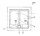
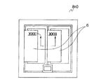
図19、20に示すように、半導体装置800はIGBT等の半導体チップ1を含む。半導体チップ1の表面には、エミッタ電極2と、ゲート電極3に接続されたゲート配線4とが設けられている。エミッタ電極2とゲート電極3の周囲、および半導体チップ1の表面を覆うように、オーバーコート膜5が設けられている。また、エミッタ電極2の上には金属膜6が設けられ、その上に半田層11を介してリード端子10が接続されている(図19には、金属膜6、リード端子10、半田層11は示さず)。
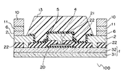
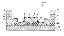
なお、図22に示すように、詳しく見れば、半導体基板1の上には、下敷酸化膜20を介してポリシリコン配線21が設けられ、その上にゲート配線4が設けられている。また、エミッタ電極2とゲート配線4との間には層間絶縁膜22が設けられている。
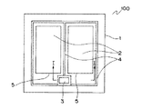
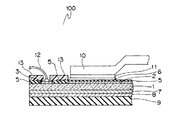
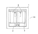
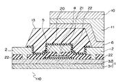
図1は、全体が100で表される、本実施の形態1にかかるダイレクトリードボンディング方式を用いた半導体装置の上面図であり、ポリイミド膜形成前の状態を示す。図2は、図1をI−I方向に見た場合の断面図であり、理解を容易にするために、図の右半分においてポリイミド膜13は省略してある。
エミッタ電極2の上には、例えばTi/Ni/Auの3層構造からなる金属膜6が設けられている。エミッタ電極2上に選択的に金属膜6を形成するためには、半導体チップ1を含むウエハの表面にメタルマスクなどを貼りあわせて金属を蒸着する方法が用いられる。金属膜6のうち、Tiはエミッタ電極2とのオーミック特性を向上させるため、Niは半田層11との接続剤として、AuはNiの酸化防止剤としての役割を果たす。
なお、金属膜6として、Ti/Ni/Auの3層構造以外に、Al/Mo/Ni/AuやAl/Ti/Ni/Auなどの積層構造を用いてもかまわない。
更に、ポリイミド膜13の形成後にメタルマスクを用いて金属層6が蒸着されるが、半導体装置110では、メタルマスクの位置がゲート配線4側にずれ、金属層6がポリイミド膜13の上まで延びて形成されている。この結果、金属層6の上に形成される半田層11、リード電極10が、ともにポリイミド膜13に重なった構成となる。
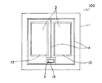
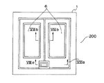
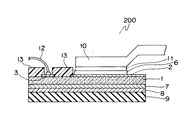
図8は、全体が200で表される、本実施の形態2にかかる半導体装置の上面図であり、図9は、図8をVIIIa−VIIIa方向に見た場合の断面図である。また、図10は、図8をVIIIb−VIIIb方向に見た場合の断面図である。図9の右半分において、ポリイミド膜13は省略してある。図8〜10において、図1〜5と同一符合は、同一又は想到箇所を示す。
図11は、全体が300で表される、本実施の形態3にかかる半導体装置の断面図である。図11中、図2と同一符合は、同一又は相当箇所を示す。
も同様の効果示す。
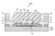
図12は、全体が400で表される、本実施の形態4にかかる半導体装置の上面図であり、図13は、図12をXII−XII方向に見た場合の断面図である。図12、13中、図1、2と同一符合は、同一又は相当箇所を示す。
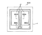
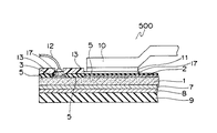
図14〜16は、全体が500で表される、本実施の形態にかかる半導体装置の上面図であり、図17、18は、それぞれ、図16をXVIa−XVIa方向、XVIb−XVIb方向に見た場合の断面図である。図14〜18において、図1、2と同一符合は、同一又は相当箇所を示す。
また、本発明は、その他のパワー半導体チップであるダイオード、CSTBT(三菱電機製IGBT)などを用いる場合にも適用できる。
更に、パワー半導体チップ以外の、HVIC(High Voltage IC)やLSIなどの集積回路にも同様に適用することができる。
Claims (8)
- ダイレクトリードボンディング方式の半導体装置であって、
半導体基板と、
該半導体基板の表面に設けられた表面電極と、
該半導体基板の表面に該表面電極に沿って設けられたゲート配線と、
該表面電極の上に設けられた金属膜と、
該金属膜の上に取り付けられたリード端子とを含み、
該ゲート配線がポリイミド膜に覆われ、該金属膜が該ポリイミド膜の上まで延在したことを特徴とする半導体装置。 - ダイレクトリードボンディング方式の半導体装置であって、
半導体基板と、
該半導体基板の表面に設けられた表面電極と、
該半導体基板の表面に該表面電極に沿って設けられたゲート配線と、
該表面電極の上に設けられた金属膜と、
該金属膜の上に取り付けられたリード端子とを含み、
該ゲート配線がポリイミド膜に覆われたことを特徴とする半導体装置。 - 上記半導体基板の表面にオプション素子が設けられ、該オプション素子も上記ポリイミドで覆われたことを特徴とする請求項1または2に記載の半導体装置。
- 上記ゲート電極と上記ポリイミド膜との間に、オーバーコート膜が設けられたことを特徴とする請求項1または2に記載の半導体装置。
- 上記ポリイミド膜の膜厚が、略10μmから略50μmであることを特徴とする請求項1または2に記載の半導体装置。
- 上記半導体基板の表面に上記ゲート配線に接続されたゲート電極が設けられ、該ゲート電極上に設けられた金属膜にリード端子が取り付けられたことを特徴とする請求項1または2に記載の半導体装置。
- 上記金属膜が、蒸着法、スパッタ法、およびメッキ法から選択される一の方法で形成されたことを特徴とする請求項1または2に記載の半導体装置。
- 上記半導体基板の裏面に裏面電極が設けられ、上記表面電極と該裏面電極との間を流れる電流が、上記ゲート配線で制御されることを特徴とする請求項1または2に記載の半導体装置。
Priority Applications (4)
| Application Number | Priority Date | Filing Date | Title |
|---|---|---|---|
| JP2005333656A JP2007142138A (ja) | 2005-11-18 | 2005-11-18 | 半導体装置 |
| US11/427,608 US20070114577A1 (en) | 2005-11-18 | 2006-06-29 | Semiconductor device |
| DE102006041575A DE102006041575A1 (de) | 2005-11-18 | 2006-09-05 | Halbleitervorrichtung |
| KR1020060087828A KR100778356B1 (ko) | 2005-11-18 | 2006-09-12 | 반도체 장치 |
Applications Claiming Priority (1)
| Application Number | Priority Date | Filing Date | Title |
|---|---|---|---|
| JP2005333656A JP2007142138A (ja) | 2005-11-18 | 2005-11-18 | 半導体装置 |
Publications (2)
| Publication Number | Publication Date |
|---|---|
| JP2007142138A true JP2007142138A (ja) | 2007-06-07 |
| JP2007142138A5 JP2007142138A5 (ja) | 2008-01-24 |
Family
ID=38047775
Family Applications (1)
| Application Number | Title | Priority Date | Filing Date |
|---|---|---|---|
| JP2005333656A Pending JP2007142138A (ja) | 2005-11-18 | 2005-11-18 | 半導体装置 |
Country Status (4)
| Country | Link |
|---|---|
| US (1) | US20070114577A1 (ja) |
| JP (1) | JP2007142138A (ja) |
| KR (1) | KR100778356B1 (ja) |
| DE (1) | DE102006041575A1 (ja) |
Cited By (23)
| Publication number | Priority date | Publication date | Assignee | Title |
|---|---|---|---|---|
| WO2010134371A1 (ja) * | 2009-05-19 | 2010-11-25 | シャープ株式会社 | 電子部品素子 |
| JP2011086852A (ja) * | 2009-10-19 | 2011-04-28 | Toyota Motor Corp | 半導体装置 |
| JP2011096699A (ja) * | 2009-10-27 | 2011-05-12 | Mitsubishi Electric Corp | 半導体装置およびその製造方法 |
| JP2011249491A (ja) * | 2010-05-26 | 2011-12-08 | Mitsubishi Electric Corp | 電力用半導体装置 |
| DE102011082781A1 (de) | 2010-09-29 | 2012-03-29 | Mitsubishi Electric Corp. | Halbleitervorrichtung |
| DE102011083243A1 (de) | 2010-10-27 | 2012-05-03 | Mitsubishi Electric Corp. | Halbleitervorrichtung |
| JP2014107489A (ja) * | 2012-11-29 | 2014-06-09 | Toyota Motor Corp | 半導体装置 |
| JP2015109334A (ja) * | 2013-12-04 | 2015-06-11 | 株式会社デンソー | 半導体装置 |
| JP2017069569A (ja) * | 2016-11-16 | 2017-04-06 | 三菱電機株式会社 | 半導体装置 |
| JP2018098283A (ja) * | 2016-12-09 | 2018-06-21 | 富士電機株式会社 | 半導体装置 |
| JP2018133445A (ja) * | 2017-02-15 | 2018-08-23 | トヨタ自動車株式会社 | 半導体装置とその製造方法 |
| JP2020077756A (ja) * | 2018-11-07 | 2020-05-21 | 富士電機株式会社 | 半導体装置および半導体装置の製造方法 |
| JP2020155464A (ja) * | 2019-03-18 | 2020-09-24 | 富士電機株式会社 | 半導体組立体および劣化検出方法 |
| JP2021002683A (ja) * | 2020-10-02 | 2021-01-07 | ローム株式会社 | 半導体装置および半導体モジュール |
| JP2021007182A (ja) * | 2020-10-19 | 2021-01-21 | 三菱電機株式会社 | 半導体装置及びその製造方法 |
| JP2021036622A (ja) * | 2020-12-03 | 2021-03-04 | 富士電機株式会社 | 半導体装置 |
| US11063004B2 (en) | 2016-11-29 | 2021-07-13 | Mitsubishi Electric Corporation | Semiconductor device, control device, and method for manufacturing semiconductor device |
| US11257812B2 (en) | 2015-02-13 | 2022-02-22 | Rohm Co., Ltd. | Semiconductor device and semiconductor module |
| JP2022130747A (ja) * | 2021-03-18 | 2022-09-06 | ローム株式会社 | 半導体装置 |
| JP2022130702A (ja) * | 2020-12-03 | 2022-09-06 | 富士電機株式会社 | 半導体装置 |
| WO2023062781A1 (ja) * | 2021-10-14 | 2023-04-20 | 三菱電機株式会社 | 半導体装置、電力変換装置および半導体装置の製造方法 |
| US11862672B2 (en) | 2012-03-12 | 2024-01-02 | Rohm Co., Ltd. | Semiconductor device, and method for manufacturing semiconductor device |
| JP7461534B2 (ja) | 2021-12-23 | 2024-04-03 | ローム株式会社 | 半導体装置 |
Families Citing this family (3)
| Publication number | Priority date | Publication date | Assignee | Title |
|---|---|---|---|---|
| DE112013007447B4 (de) | 2013-09-19 | 2022-01-27 | Mitsubishi Electric Corporation | Halbleitervorrichtung |
| CN111816652B (zh) * | 2020-05-27 | 2024-07-16 | 华为技术有限公司 | 一种集成有温度传感器的igbt芯片 |
| JP2022154006A (ja) * | 2021-03-30 | 2022-10-13 | ローム株式会社 | 半導体装置、および半導体装置の製造方法 |
Citations (9)
| Publication number | Priority date | Publication date | Assignee | Title |
|---|---|---|---|---|
| JPS6260236A (ja) * | 1985-09-10 | 1987-03-16 | Tdk Corp | 縦形半導体装置およびその製造方法 |
| JPH08227996A (ja) * | 1995-02-20 | 1996-09-03 | Fuji Electric Co Ltd | 半導体装置 |
| JP2002090422A (ja) * | 2000-09-13 | 2002-03-27 | Toshiba Corp | 半導体装置及びその製造方法 |
| JP2002252351A (ja) * | 2001-02-26 | 2002-09-06 | Sanyo Electric Co Ltd | 半導体装置 |
| JP2003133329A (ja) * | 2001-08-09 | 2003-05-09 | Denso Corp | 半導体装置 |
| JP2004111885A (ja) * | 2002-07-23 | 2004-04-08 | Toshiba Corp | 半導体装置 |
| JP2005116962A (ja) * | 2003-10-10 | 2005-04-28 | Denso Corp | パッケージ型半導体装置 |
| JP2005167075A (ja) * | 2003-12-04 | 2005-06-23 | Denso Corp | 半導体装置 |
| JP2005203548A (ja) * | 2004-01-15 | 2005-07-28 | Honda Motor Co Ltd | 半導体装置のモジュール構造 |
Family Cites Families (11)
| Publication number | Priority date | Publication date | Assignee | Title |
|---|---|---|---|---|
| JP2557898B2 (ja) * | 1987-07-31 | 1996-11-27 | 株式会社東芝 | 半導体装置 |
| US5637922A (en) * | 1994-02-07 | 1997-06-10 | General Electric Company | Wireless radio frequency power semiconductor devices using high density interconnect |
| US5795833A (en) * | 1996-08-01 | 1998-08-18 | Taiwan Semiconductor Manufacturing Company, Ltd | Method for fabricating passivation layers over metal lines |
| JPH10223624A (ja) * | 1997-02-06 | 1998-08-21 | Nec Yamagata Ltd | 半導体装置の製造方法 |
| JP4932088B2 (ja) * | 2001-02-19 | 2012-05-16 | ルネサスエレクトロニクス株式会社 | 絶縁ゲート型半導体装置の製造方法 |
| US20020163062A1 (en) * | 2001-02-26 | 2002-11-07 | International Business Machines Corporation | Multiple material stacks with a stress relief layer between a metal structure and a passivation layer |
| US6803667B2 (en) * | 2001-08-09 | 2004-10-12 | Denso Corporation | Semiconductor device having a protective film |
| JP3673231B2 (ja) * | 2002-03-07 | 2005-07-20 | 三菱電機株式会社 | 絶縁ゲート型半導体装置及びゲート配線構造の製造方法 |
| JP3931138B2 (ja) * | 2002-12-25 | 2007-06-13 | 三菱電機株式会社 | 電力用半導体装置及び電力用半導体装置の製造方法 |
| JP2004349316A (ja) * | 2003-05-20 | 2004-12-09 | Renesas Technology Corp | 半導体装置及びその製造方法 |
| US8049338B2 (en) * | 2006-04-07 | 2011-11-01 | General Electric Company | Power semiconductor module and fabrication method |
-
2005
- 2005-11-18 JP JP2005333656A patent/JP2007142138A/ja active Pending
-
2006
- 2006-06-29 US US11/427,608 patent/US20070114577A1/en not_active Abandoned
- 2006-09-05 DE DE102006041575A patent/DE102006041575A1/de not_active Withdrawn
- 2006-09-12 KR KR1020060087828A patent/KR100778356B1/ko not_active IP Right Cessation
Patent Citations (9)
| Publication number | Priority date | Publication date | Assignee | Title |
|---|---|---|---|---|
| JPS6260236A (ja) * | 1985-09-10 | 1987-03-16 | Tdk Corp | 縦形半導体装置およびその製造方法 |
| JPH08227996A (ja) * | 1995-02-20 | 1996-09-03 | Fuji Electric Co Ltd | 半導体装置 |
| JP2002090422A (ja) * | 2000-09-13 | 2002-03-27 | Toshiba Corp | 半導体装置及びその製造方法 |
| JP2002252351A (ja) * | 2001-02-26 | 2002-09-06 | Sanyo Electric Co Ltd | 半導体装置 |
| JP2003133329A (ja) * | 2001-08-09 | 2003-05-09 | Denso Corp | 半導体装置 |
| JP2004111885A (ja) * | 2002-07-23 | 2004-04-08 | Toshiba Corp | 半導体装置 |
| JP2005116962A (ja) * | 2003-10-10 | 2005-04-28 | Denso Corp | パッケージ型半導体装置 |
| JP2005167075A (ja) * | 2003-12-04 | 2005-06-23 | Denso Corp | 半導体装置 |
| JP2005203548A (ja) * | 2004-01-15 | 2005-07-28 | Honda Motor Co Ltd | 半導体装置のモジュール構造 |
Cited By (40)
| Publication number | Priority date | Publication date | Assignee | Title |
|---|---|---|---|---|
| WO2010134371A1 (ja) * | 2009-05-19 | 2010-11-25 | シャープ株式会社 | 電子部品素子 |
| JP2011086852A (ja) * | 2009-10-19 | 2011-04-28 | Toyota Motor Corp | 半導体装置 |
| JP2011096699A (ja) * | 2009-10-27 | 2011-05-12 | Mitsubishi Electric Corp | 半導体装置およびその製造方法 |
| JP2011249491A (ja) * | 2010-05-26 | 2011-12-08 | Mitsubishi Electric Corp | 電力用半導体装置 |
| US8823151B2 (en) | 2010-09-29 | 2014-09-02 | Mitsubishi Electric Corporation | Semiconductor device |
| DE102011082781A1 (de) | 2010-09-29 | 2012-03-29 | Mitsubishi Electric Corp. | Halbleitervorrichtung |
| CN102437138A (zh) * | 2010-09-29 | 2012-05-02 | 三菱电机株式会社 | 半导体装置 |
| US10529656B2 (en) | 2010-09-29 | 2020-01-07 | Mitsubishi Electric Corporation | Semiconductor device |
| DE102011082781B4 (de) * | 2010-09-29 | 2016-07-07 | Mitsubishi Electric Corp. | Halbleitervorrichtung mit einer plattenelektrode zum verbinden einer mehrzahl an halbleiterchips |
| DE102011083243A1 (de) | 2010-10-27 | 2012-05-03 | Mitsubishi Electric Corp. | Halbleitervorrichtung |
| US8692244B2 (en) | 2010-10-27 | 2014-04-08 | Mitsubishi Electric Corporation | Semiconductor device |
| JP2012094669A (ja) * | 2010-10-27 | 2012-05-17 | Mitsubishi Electric Corp | 半導体装置 |
| US11862672B2 (en) | 2012-03-12 | 2024-01-02 | Rohm Co., Ltd. | Semiconductor device, and method for manufacturing semiconductor device |
| JP2014107489A (ja) * | 2012-11-29 | 2014-06-09 | Toyota Motor Corp | 半導体装置 |
| JP2015109334A (ja) * | 2013-12-04 | 2015-06-11 | 株式会社デンソー | 半導体装置 |
| US11916069B2 (en) | 2015-02-13 | 2024-02-27 | Rohm Co., Ltd. | Semiconductor device and semiconductor module |
| US11670633B2 (en) | 2015-02-13 | 2023-06-06 | Rohm Co., Ltd. | Semiconductor device and semiconductor module |
| US11257812B2 (en) | 2015-02-13 | 2022-02-22 | Rohm Co., Ltd. | Semiconductor device and semiconductor module |
| US11495595B2 (en) | 2015-02-13 | 2022-11-08 | Rohm Co., Ltd. | Semiconductor device and semiconductor module |
| JP2017069569A (ja) * | 2016-11-16 | 2017-04-06 | 三菱電機株式会社 | 半導体装置 |
| DE112016007485B4 (de) | 2016-11-29 | 2024-10-24 | Mitsubishi Electric Corporation | Halbleitervorrichtung, Steuervorrichtung, und Verfahren zur Herstellung der Halbleitervorrichtung |
| US11063004B2 (en) | 2016-11-29 | 2021-07-13 | Mitsubishi Electric Corporation | Semiconductor device, control device, and method for manufacturing semiconductor device |
| JP2018098283A (ja) * | 2016-12-09 | 2018-06-21 | 富士電機株式会社 | 半導体装置 |
| JP2018133445A (ja) * | 2017-02-15 | 2018-08-23 | トヨタ自動車株式会社 | 半導体装置とその製造方法 |
| JP7167639B2 (ja) | 2018-11-07 | 2022-11-09 | 富士電機株式会社 | 半導体装置および半導体装置の製造方法 |
| JP2020077756A (ja) * | 2018-11-07 | 2020-05-21 | 富士電機株式会社 | 半導体装置および半導体装置の製造方法 |
| JP7247681B2 (ja) | 2019-03-18 | 2023-03-29 | 富士電機株式会社 | 半導体組立体 |
| JP2020155464A (ja) * | 2019-03-18 | 2020-09-24 | 富士電機株式会社 | 半導体組立体および劣化検出方法 |
| US11189534B2 (en) | 2019-03-18 | 2021-11-30 | Fuji Electric Co., Ltd. | Semiconductor assembly and deterioration detection method |
| JP7001785B2 (ja) | 2020-10-02 | 2022-01-20 | ローム株式会社 | 半導体装置および半導体モジュール |
| JP2021002683A (ja) * | 2020-10-02 | 2021-01-07 | ローム株式会社 | 半導体装置および半導体モジュール |
| JP2021007182A (ja) * | 2020-10-19 | 2021-01-21 | 三菱電機株式会社 | 半導体装置及びその製造方法 |
| JP7160079B2 (ja) | 2020-12-03 | 2022-10-25 | 富士電機株式会社 | 半導体装置 |
| JP7302715B2 (ja) | 2020-12-03 | 2023-07-04 | 富士電機株式会社 | 半導体装置 |
| JP2021036622A (ja) * | 2020-12-03 | 2021-03-04 | 富士電機株式会社 | 半導体装置 |
| JP2022130702A (ja) * | 2020-12-03 | 2022-09-06 | 富士電機株式会社 | 半導体装置 |
| JP7194855B2 (ja) | 2021-03-18 | 2022-12-22 | ローム株式会社 | 半導体装置 |
| JP2022130747A (ja) * | 2021-03-18 | 2022-09-06 | ローム株式会社 | 半導体装置 |
| WO2023062781A1 (ja) * | 2021-10-14 | 2023-04-20 | 三菱電機株式会社 | 半導体装置、電力変換装置および半導体装置の製造方法 |
| JP7461534B2 (ja) | 2021-12-23 | 2024-04-03 | ローム株式会社 | 半導体装置 |
Also Published As
| Publication number | Publication date |
|---|---|
| KR100778356B1 (ko) | 2007-11-22 |
| US20070114577A1 (en) | 2007-05-24 |
| DE102006041575A1 (de) | 2007-06-06 |
| KR20070053094A (ko) | 2007-05-23 |
Similar Documents
| Publication | Publication Date | Title |
|---|---|---|
| JP2007142138A (ja) | 半導体装置 | |
| US7659611B2 (en) | Vertical power semiconductor component, semiconductor device and methods for the production thereof | |
| JP5073992B2 (ja) | 半導体装置 | |
| JP3750680B2 (ja) | パッケージ型半導体装置 | |
| US10115798B2 (en) | Semiconductor device and method of manufacturing the same | |
| TW200929408A (en) | Wafer level chip scale packaging | |
| US11417623B2 (en) | Semiconductor chip and semiconductor device including a copper pillar and an intermediate layer | |
| JP2007019215A (ja) | 半導体装置及びその製法 | |
| JP7280261B2 (ja) | 半導体素子および半導体装置 | |
| JP4073876B2 (ja) | 半導体装置 | |
| JP2008235728A (ja) | 半導体装置 | |
| JP6579989B2 (ja) | 半導体装置および半導体装置の製造方法 | |
| JP2005019798A (ja) | モールド型半導体装置及びその製造方法 | |
| US10217832B2 (en) | Semiconductor device | |
| WO2022270305A1 (ja) | 半導体装置、および半導体装置の製造方法 | |
| WO2023189480A1 (ja) | 半導体素子および半導体装置 | |
| JP4962409B2 (ja) | 半導体装置及びその製法 | |
| WO2023112662A1 (ja) | 半導体モジュールおよび半導体装置 | |
| JP4852876B2 (ja) | 半導体装置 | |
| JP2009141083A (ja) | 半導体装置 | |
| JP2009038140A (ja) | 半導体装置およびその製造方法 | |
| US20180197984A1 (en) | Semiconductor device | |
| KR20020080234A (ko) | 반도체장치 | |
| JP2008252114A (ja) | 半導体装置 | |
| JP2005167109A (ja) | 半導体装置及びその製造方法 |
Legal Events
| Date | Code | Title | Description |
|---|---|---|---|
| A521 | Request for written amendment filed |
Free format text: JAPANESE INTERMEDIATE CODE: A523 Effective date: 20071204 |
|
| A621 | Written request for application examination |
Free format text: JAPANESE INTERMEDIATE CODE: A621 Effective date: 20071204 |
|
| A977 | Report on retrieval |
Free format text: JAPANESE INTERMEDIATE CODE: A971007 Effective date: 20091125 |
|
| A131 | Notification of reasons for refusal |
Free format text: JAPANESE INTERMEDIATE CODE: A131 Effective date: 20091201 |
|
| A02 | Decision of refusal |
Free format text: JAPANESE INTERMEDIATE CODE: A02 Effective date: 20100330 |
