EP4020596B1 - Anzeigevorrichtung und herstellungsverfahren dafür - Google Patents
Anzeigevorrichtung und herstellungsverfahren dafür Download PDFInfo
- Publication number
- EP4020596B1 EP4020596B1 EP19933233.9A EP19933233A EP4020596B1 EP 4020596 B1 EP4020596 B1 EP 4020596B1 EP 19933233 A EP19933233 A EP 19933233A EP 4020596 B1 EP4020596 B1 EP 4020596B1
- Authority
- EP
- European Patent Office
- Prior art keywords
- transistor
- doped region
- electrode
- base substrate
- type
- Prior art date
- Legal status (The legal status is an assumption and is not a legal conclusion. Google has not performed a legal analysis and makes no representation as to the accuracy of the status listed.)
- Active
Links
Images


Classifications
-
- H—ELECTRICITY
- H10—SEMICONDUCTOR DEVICES; ELECTRIC SOLID-STATE DEVICES NOT OTHERWISE PROVIDED FOR
- H10K—ORGANIC ELECTRIC SOLID-STATE DEVICES
- H10K59/00—Integrated devices, or assemblies of multiple devices, comprising at least one organic light-emitting element covered by group H10K50/00
- H10K59/10—OLED displays
- H10K59/12—Active-matrix OLED [AMOLED] displays
- H10K59/124—Insulating layers formed between TFT elements and OLED elements
-
- G—PHYSICS
- G09—EDUCATION; CRYPTOGRAPHY; DISPLAY; ADVERTISING; SEALS
- G09G—ARRANGEMENTS OR CIRCUITS FOR CONTROL OF INDICATING DEVICES USING STATIC MEANS TO PRESENT VARIABLE INFORMATION
- G09G3/00—Control arrangements or circuits, of interest only in connection with visual indicators other than cathode-ray tubes
- G09G3/20—Control arrangements or circuits, of interest only in connection with visual indicators other than cathode-ray tubes for presentation of an assembly of a number of characters, e.g. a page, by composing the assembly by combination of individual elements arranged in a matrix no fixed position being assigned to or needed to be assigned to the individual characters or partial characters
- G09G3/22—Control arrangements or circuits, of interest only in connection with visual indicators other than cathode-ray tubes for presentation of an assembly of a number of characters, e.g. a page, by composing the assembly by combination of individual elements arranged in a matrix no fixed position being assigned to or needed to be assigned to the individual characters or partial characters using controlled light sources
- G09G3/30—Control arrangements or circuits, of interest only in connection with visual indicators other than cathode-ray tubes for presentation of an assembly of a number of characters, e.g. a page, by composing the assembly by combination of individual elements arranged in a matrix no fixed position being assigned to or needed to be assigned to the individual characters or partial characters using controlled light sources using electroluminescent panels
- G09G3/32—Control arrangements or circuits, of interest only in connection with visual indicators other than cathode-ray tubes for presentation of an assembly of a number of characters, e.g. a page, by composing the assembly by combination of individual elements arranged in a matrix no fixed position being assigned to or needed to be assigned to the individual characters or partial characters using controlled light sources using electroluminescent panels semiconductive, e.g. using light-emitting diodes [LED]
- G09G3/3208—Control arrangements or circuits, of interest only in connection with visual indicators other than cathode-ray tubes for presentation of an assembly of a number of characters, e.g. a page, by composing the assembly by combination of individual elements arranged in a matrix no fixed position being assigned to or needed to be assigned to the individual characters or partial characters using controlled light sources using electroluminescent panels semiconductive, e.g. using light-emitting diodes [LED] organic, e.g. using organic light-emitting diodes [OLED]
- G09G3/3225—Control arrangements or circuits, of interest only in connection with visual indicators other than cathode-ray tubes for presentation of an assembly of a number of characters, e.g. a page, by composing the assembly by combination of individual elements arranged in a matrix no fixed position being assigned to or needed to be assigned to the individual characters or partial characters using controlled light sources using electroluminescent panels semiconductive, e.g. using light-emitting diodes [LED] organic, e.g. using organic light-emitting diodes [OLED] using an active matrix
- G09G3/3233—Control arrangements or circuits, of interest only in connection with visual indicators other than cathode-ray tubes for presentation of an assembly of a number of characters, e.g. a page, by composing the assembly by combination of individual elements arranged in a matrix no fixed position being assigned to or needed to be assigned to the individual characters or partial characters using controlled light sources using electroluminescent panels semiconductive, e.g. using light-emitting diodes [LED] organic, e.g. using organic light-emitting diodes [OLED] using an active matrix with pixel circuitry controlling the current through the light-emitting element
-
- H—ELECTRICITY
- H10—SEMICONDUCTOR DEVICES; ELECTRIC SOLID-STATE DEVICES NOT OTHERWISE PROVIDED FOR
- H10D—INORGANIC ELECTRIC SEMICONDUCTOR DEVICES
- H10D30/00—Field-effect transistors [FET]
- H10D30/60—Insulated-gate field-effect transistors [IGFET]
- H10D30/67—Thin-film transistors [TFT]
- H10D30/6704—Thin-film transistors [TFT] having supplementary regions or layers in the thin films or in the insulated bulk substrates for controlling properties of the device
- H10D30/6713—Thin-film transistors [TFT] having supplementary regions or layers in the thin films or in the insulated bulk substrates for controlling properties of the device characterised by the properties of the source or drain regions, e.g. compositions or sectional shapes
- H10D30/6715—Thin-film transistors [TFT] having supplementary regions or layers in the thin films or in the insulated bulk substrates for controlling properties of the device characterised by the properties of the source or drain regions, e.g. compositions or sectional shapes characterised by the doping profiles, e.g. having lightly-doped source or drain extensions
- H10D30/6717—Thin-film transistors [TFT] having supplementary regions or layers in the thin films or in the insulated bulk substrates for controlling properties of the device characterised by the properties of the source or drain regions, e.g. compositions or sectional shapes characterised by the doping profiles, e.g. having lightly-doped source or drain extensions the source and the drain regions being asymmetrical
-
- H—ELECTRICITY
- H10—SEMICONDUCTOR DEVICES; ELECTRIC SOLID-STATE DEVICES NOT OTHERWISE PROVIDED FOR
- H10D—INORGANIC ELECTRIC SEMICONDUCTOR DEVICES
- H10D30/00—Field-effect transistors [FET]
- H10D30/60—Insulated-gate field-effect transistors [IGFET]
- H10D30/67—Thin-film transistors [TFT]
- H10D30/6704—Thin-film transistors [TFT] having supplementary regions or layers in the thin films or in the insulated bulk substrates for controlling properties of the device
- H10D30/6713—Thin-film transistors [TFT] having supplementary regions or layers in the thin films or in the insulated bulk substrates for controlling properties of the device characterised by the properties of the source or drain regions, e.g. compositions or sectional shapes
- H10D30/6715—Thin-film transistors [TFT] having supplementary regions or layers in the thin films or in the insulated bulk substrates for controlling properties of the device characterised by the properties of the source or drain regions, e.g. compositions or sectional shapes characterised by the doping profiles, e.g. having lightly-doped source or drain extensions
- H10D30/6719—Thin-film transistors [TFT] having supplementary regions or layers in the thin films or in the insulated bulk substrates for controlling properties of the device characterised by the properties of the source or drain regions, e.g. compositions or sectional shapes characterised by the doping profiles, e.g. having lightly-doped source or drain extensions having significant overlap between the lightly-doped drains and the gate electrodes, e.g. gate-overlapped LDD [GOLDD] TFTs
-
- H—ELECTRICITY
- H10—SEMICONDUCTOR DEVICES; ELECTRIC SOLID-STATE DEVICES NOT OTHERWISE PROVIDED FOR
- H10D—INORGANIC ELECTRIC SEMICONDUCTOR DEVICES
- H10D84/00—Integrated devices formed in or on semiconductor substrates that comprise only semiconducting layers, e.g. on Si wafers or on GaAs-on-Si wafers
- H10D84/01—Manufacture or treatment
-
- H—ELECTRICITY
- H10—SEMICONDUCTOR DEVICES; ELECTRIC SOLID-STATE DEVICES NOT OTHERWISE PROVIDED FOR
- H10D—INORGANIC ELECTRIC SEMICONDUCTOR DEVICES
- H10D86/00—Integrated devices formed in or on insulating or conducting substrates, e.g. formed in silicon-on-insulator [SOI] substrates or on stainless steel or glass substrates
- H10D86/01—Manufacture or treatment
-
- H—ELECTRICITY
- H10—SEMICONDUCTOR DEVICES; ELECTRIC SOLID-STATE DEVICES NOT OTHERWISE PROVIDED FOR
- H10D—INORGANIC ELECTRIC SEMICONDUCTOR DEVICES
- H10D86/00—Integrated devices formed in or on insulating or conducting substrates, e.g. formed in silicon-on-insulator [SOI] substrates or on stainless steel or glass substrates
- H10D86/201—Integrated devices formed in or on insulating or conducting substrates, e.g. formed in silicon-on-insulator [SOI] substrates or on stainless steel or glass substrates the substrates comprising an insulating layer on a semiconductor body, e.g. SOI
-
- H—ELECTRICITY
- H10—SEMICONDUCTOR DEVICES; ELECTRIC SOLID-STATE DEVICES NOT OTHERWISE PROVIDED FOR
- H10D—INORGANIC ELECTRIC SEMICONDUCTOR DEVICES
- H10D86/00—Integrated devices formed in or on insulating or conducting substrates, e.g. formed in silicon-on-insulator [SOI] substrates or on stainless steel or glass substrates
- H10D86/40—Integrated devices formed in or on insulating or conducting substrates, e.g. formed in silicon-on-insulator [SOI] substrates or on stainless steel or glass substrates characterised by multiple TFTs
- H10D86/431—Integrated devices formed in or on insulating or conducting substrates, e.g. formed in silicon-on-insulator [SOI] substrates or on stainless steel or glass substrates characterised by multiple TFTs having different compositions, shapes, layouts or thicknesses of gate insulators in different TFTs
-
- H—ELECTRICITY
- H10—SEMICONDUCTOR DEVICES; ELECTRIC SOLID-STATE DEVICES NOT OTHERWISE PROVIDED FOR
- H10D—INORGANIC ELECTRIC SEMICONDUCTOR DEVICES
- H10D86/00—Integrated devices formed in or on insulating or conducting substrates, e.g. formed in silicon-on-insulator [SOI] substrates or on stainless steel or glass substrates
- H10D86/40—Integrated devices formed in or on insulating or conducting substrates, e.g. formed in silicon-on-insulator [SOI] substrates or on stainless steel or glass substrates characterised by multiple TFTs
- H10D86/441—Interconnections, e.g. scanning lines
-
- H—ELECTRICITY
- H10—SEMICONDUCTOR DEVICES; ELECTRIC SOLID-STATE DEVICES NOT OTHERWISE PROVIDED FOR
- H10D—INORGANIC ELECTRIC SEMICONDUCTOR DEVICES
- H10D86/00—Integrated devices formed in or on insulating or conducting substrates, e.g. formed in silicon-on-insulator [SOI] substrates or on stainless steel or glass substrates
- H10D86/40—Integrated devices formed in or on insulating or conducting substrates, e.g. formed in silicon-on-insulator [SOI] substrates or on stainless steel or glass substrates characterised by multiple TFTs
- H10D86/60—Integrated devices formed in or on insulating or conducting substrates, e.g. formed in silicon-on-insulator [SOI] substrates or on stainless steel or glass substrates characterised by multiple TFTs wherein the TFTs are in active matrices
-
- H—ELECTRICITY
- H10—SEMICONDUCTOR DEVICES; ELECTRIC SOLID-STATE DEVICES NOT OTHERWISE PROVIDED FOR
- H10K—ORGANIC ELECTRIC SOLID-STATE DEVICES
- H10K59/00—Integrated devices, or assemblies of multiple devices, comprising at least one organic light-emitting element covered by group H10K50/00
- H10K59/10—OLED displays
- H10K59/12—Active-matrix OLED [AMOLED] displays
- H10K59/121—Active-matrix OLED [AMOLED] displays characterised by the geometry or disposition of pixel elements
- H10K59/1213—Active-matrix OLED [AMOLED] displays characterised by the geometry or disposition of pixel elements the pixel elements being TFTs
-
- H—ELECTRICITY
- H10—SEMICONDUCTOR DEVICES; ELECTRIC SOLID-STATE DEVICES NOT OTHERWISE PROVIDED FOR
- H10K—ORGANIC ELECTRIC SOLID-STATE DEVICES
- H10K59/00—Integrated devices, or assemblies of multiple devices, comprising at least one organic light-emitting element covered by group H10K50/00
- H10K59/10—OLED displays
- H10K59/12—Active-matrix OLED [AMOLED] displays
- H10K59/123—Connection of the pixel electrodes to the thin film transistors [TFT]
-
- H—ELECTRICITY
- H10—SEMICONDUCTOR DEVICES; ELECTRIC SOLID-STATE DEVICES NOT OTHERWISE PROVIDED FOR
- H10K—ORGANIC ELECTRIC SOLID-STATE DEVICES
- H10K59/00—Integrated devices, or assemblies of multiple devices, comprising at least one organic light-emitting element covered by group H10K50/00
- H10K59/10—OLED displays
- H10K59/12—Active-matrix OLED [AMOLED] displays
- H10K59/131—Interconnections, e.g. wiring lines or terminals
-
- H—ELECTRICITY
- H10—SEMICONDUCTOR DEVICES; ELECTRIC SOLID-STATE DEVICES NOT OTHERWISE PROVIDED FOR
- H10K—ORGANIC ELECTRIC SOLID-STATE DEVICES
- H10K59/00—Integrated devices, or assemblies of multiple devices, comprising at least one organic light-emitting element covered by group H10K50/00
- H10K59/10—OLED displays
- H10K59/12—Active-matrix OLED [AMOLED] displays
- H10K59/1201—Manufacture or treatment
Definitions
- Embodiments of the present disclosure relate to a display device and a manufacturing method thereof.
- the micro organic light-emitting diode (Micro-OLED) display device is a new type of OLED display device that uses a silicon substrate as a substrate, and is also called a silicon-based organic light-emitting diode (silicon-based OLED) display device.
- the silicon-based OLED display device has the advantages of small size and high resolution, and is manufactured using a mature CMOS integrated circuit process, which can realize active addressing of pixels, and can manufacture a variety of functional circuits including a TCON (timing control) circuit, a OCP (Operation Control) circuit, and the like on the silicon substrate, thereby implementing light weight.
- TCON timing control
- OCP Operaation Control
- the pixel circuit comprises a power supply terminal; a control thin film transistor; a drive thin film transistor; a storage capacitor; a light-emitting device, the pixel circuit further comprises a voltage division control module and a voltage division capacitor, the voltage division control module is used for charging the storage capacitor in the pre-charging phase of the pixel circuit, so that voltage of the gate of the drive thin film transistor becomes a reference voltage, and the voltage division control module is capable of outputting a low level to the second end of the storage capacitor in the compensation phase of the pixel circuit.
- a first end of the voltage division capacitor is connected to the first end of the storage capacitor, a second end thereof is connected to the cathode of the light-emitting device.
- US2005/056832 A1 directs to an electronic device having high reliability and high color reproducibility.
- a pixel structure is made such that a switching FET 201 and an electric current controlling FET 202 are formed on a single crystal semiconductor substrate 11, and an EL element 203 is electrically connected to the electric current controlling FET 202.
- the fluctuation in characteristics of the electric current controlling FET 202 is very low among pixels, and an image with high color reproducibility can be obtained.
- the electronic device having high reliability can be obtained.
- US5830787 A directs to a method for fabricating a thin film transistor (TFT), including the steps of forming a semiconductor layer on a substrate; forming an insulating oxide layer on the semiconductor layer; forming a polysilicon layer on the insulating layer; etching the polysilicon layer to form a gate electrode having tapered sides; carrying out an oxidation process on exposed surfaces of the gate electrode and the polysilicon layer surrounding the gate electrode resulting in the oxide layer thereby formed being thicker below the bottom edges of the tapered sides of the gate electrode than on other portions of the gate electrode and the surrounding polysilicon layer; and forming impurity regions in the semiconductor layer on opposite sides of the gate electrode to thereby form a transistor.
- the TFT thereby formed has a tapered gate and reduced OFF current.
- An objective of the present disclosure is to provide a display device, and a manufacturing method of a display device.
- connection is not intended to define a physical connection or mechanical connection, but may include an electrical connection, directly or indirectly.
- "On,” “under,” “right,” “left” and the like are only used to indicate relative position relationship, and when the position of the object which is described is changed, the relative position relationship may be changed accordingly.
- silicon-based OLED display panels are widely used in the field of near-eye display such as virtual reality (VR) or augmented reality (AR), and users are increasingly demanding better display quality, for example, need to achieve higher resolution and PPI (Pixels Per Inch).
- VR virtual reality
- AR augmented reality
- PPI Pixel Per Inch
- the layout of a display device needs to be designed to reduce the layout area that is occupied, so that more pixel units can be provided in the display region of the same size, thereby achieving high PPI.
- the display device and the manufacturing method thereof provided by at least one embodiment of the present disclosure can reduce the layout area occupied by the display device through layout design, so that the display device can more easily achieve high PPI.
- at least one embodiment of the present disclosure further provides a structural design of a transistor that can reduce or avoid the risk of breakdown under the action of a high voltage.
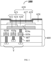
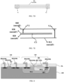
- FIG. 1 is a schematic structural diagram of a display substrate 1000.
- the display substrate 1000 includes a base substrate 600 and a light-emitting element 620.
- the light-emitting element 620 is provided on the base substrate 600, and a first electrode 621 of the light-emitting element 620 is closer to the base substrate 600 than a second electrode 629 of the light-emitting element 620.
- the base substrate 600 is a silicon-based base substrate, and the embodiments of the present disclosure include but are not limited this case.
- the semiconductor manufacturing process used on silicon-based substrates is mature and has stable performance, which is beneficial to the manufacture of micro display devices.
- the silicon-based base substrate 600 includes a driving circuit, and the driving circuit is electrically connected to the light-emitting element 620 for driving the light-emitting element 620 to emit light.
- the driving circuit includes a transistor T.
- the specific circuit structure of the driving circuit may be set according to actual needs.
- FIG. 1 does not illustrate the entire structure of the driving circuit, the driving circuit may further include, for example, other transistors, and for another example, a storage capacitor, etc., and the embodiments of the present disclosure are not limited in this aspect.
- the transistor T includes a gate electrode G, a source electrode S, and a drain electrode D.
- the three electrodes respectively correspond to three electrode connection portions.
- the gate electrode G is electrically connected to a gate electrode connection portion 610g
- the source electrode S is electrically connected to a source electrode connection portion 610s
- the drain electrode D is electrically connected to a drain electrode connection portion 610d.
- the three electrodes are correspondingly electrically connected to the three electrode connection portions through tungsten via holes 605.
- the source electrode connection portion 610s is electrically connected to the first electrode 621 of the light-emitting element 620 through a tungsten via hole.
- the source electrode connection portion 610s is electrically connected to a metal reflective layer 622 of the first electrode 621 through the tungsten via hole, and in the first electrode 621, a transparent conductive layer 626 is electrically connected to the metal reflective layer 622 through a via hole 624a in an inorganic insulating layer 624.
- an electrical signal provided by a power supply line can be transmitted to the transparent conductive layer 626 through the source electrode S of the transistor T, the source electrode connection portion 610s, and the metal reflective layer 622. Because a voltage difference is formed between the transparent conductive layer 626 and the second electrode 629, an electric field is formed between the transparent conductive layer 626 and the second electrode 629, holes and electrons are injected into a light-emitting functional layer 627, and the light-emitting functional layer 627 emits light under the action of the electric field.
- the positions of the source electrode S and the drain electrode D are interchangeable (correspondingly, the positions of the source electrode connection portion 610s and the drain electrode connection portion 610d are also interchangeable), that is, the light-emitting element 620 and one of the source electrode S and the drain electrode D of the transistor (that is, the source electrode S or the drain electrode D) may be electrically connected to each other.
- the materials of the gate electrode connection portion 610g, the source electrode connection portion 610s, and the drain electrode connection portion 610d may include metal materials.
- an anti-oxidation layer 607 may be provided on at least one side (for example, an upper side and/or a lower side) of each of the gate electrode connection part 610g, the source electrode connection part 610s, and the drain electrode connection part 610d, which can effectively prevent these electrode connection portions from being oxidized and improve conductivity of these electrode connection portions.
- the display substrate 1000 further includes a defining layer 628 for defining the light-emitting functional layer 627, and the defining layer 628 defines the light-emitting functional layer 627 in an opening 728a so as to avoid the crosstalk of sub-pixels which are adjacent to each other.
- the via hole 624a in the inorganic insulating layer 624 may be disposed between the transparent conductive layer 626 and an edge region of the metal reflective layer 622.
- the orthographic projection of the light-emitting functional layer 627 on the base substrate 600 and the orthographic projection of the via hole 624a on the base substrate 600 are both within the orthographic projection of the metal reflective layer 622 on the base substrate 600, and there is no overlap between the orthographic projection of the light-emitting functional layer 627 on the base substrate 600 and the orthographic projection of the via hole 624a on the base substrate 600, so that when the metal reflective layer reflects the light emitted by the light-emitting functional layer 627, the via hole 624a has basically no effect on the reflection process.
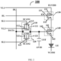
- the claimed invention provides a display device 100, and the display device 100 includes a base substrate and at least one pixel circuit provided on the base substrate and a light-emitting element driven by the pixel circuit.
- the base substrate is, for example, a silicon-based base substrate, which may be a bulk silicon substrate or a silicon-on-insulator (SOI) substrate.
- the pixel circuit may be manufactured in the base substrate by a silicon semiconductor process (for example, a CMOS process), and the light-emitting element is manufactured on a silicon substrate having the pixel circuit.
- the display device 100 is described below with reference to FIG. 2 and FIG. 3 . It should be noted that the base substrate is not illustrated in FIG. 2 and FIG. 3 . For the base substrate, reference may be made to the base substrate 600 illustrated in FIG. 1 .
- the pixel circuit includes a driving transistor 140, a first transistor 110, a second transistor 120 and a third transistor 130. It should be noted that, in some embodiments, the pixel circuit may not include the third transistor 130, and the embodiments of the present disclosure are not limited in this aspect.
- the driving transistor 140 includes a control electrode 143, a first electrode 141, and a second electrode 142, and the driving transistor 140 is configured to control a driving current, which flows through the first electrode 141 of the driving transistor 140 and the second electrode 142 of the driving transistor 140, for driving a light-emitting element LE to emit light according to the voltage of the control electrode 143 of the driving transistor 140.
- the light-emitting element LE can emit light of different intensities according to the magnitude of the driving current.
- the source electrode and drain electrode of the transistor used in the embodiment of the present disclosure may be symmetrical in structure, so that the source electrode and the drain electrode may be structurally indistinguishable.
- one electrode is directly described as the first electrode, and the other electrode is described as the second electrode, so that in the embodiments of the present disclosure, the first electrodes and the second electrodes of all or part of the transistors are interchangeable as needed.
- the first electrodes of the transistors described in the embodiments of the present disclosure may be source electrodes and the second electrodes may be drain electrodes; or, the first electrodes of the transistors may be drain electrodes and the second electrodes may be source electrodes.
- the following embodiments are described by taking the case where the first electrodes of the transistors may be drain electrodes and the second electrodes may be source electrodes as an example, and are not repeated here for simplicity.
- the first transistor 110 is connected to the control electrode 143 of the driving transistor 140 and is configured to write a data signal DATA to the control electrode 143 of the driving transistor 140 in response to a first scan signal SCAN1.
- the second transistor 120 is connected to the control electrode 143 of the driving transistor 140 and is configured to write the data signal DATA to the control electrode 143 of the driving transistor 140 in response to a second scan signal SCAN2.
- the third transistor 130 is connected to the first electrode 141 of the driving transistor 140 and is configured to apply a first power supply voltage ELVDD to the first electrode 141 of the driving transistor 140 in response to a light-emitting control signal EN.
- the first power supply voltage ELVDD in the embodiments of the present disclosure is a high-level voltage, and for example, the first power supply voltage ELVDD is at 5V.
- the first electrode 111 for example, a drain electrode
- the first electrode 121 for example, a drain electrode
- the second transistor 120 are connected to obtain a common electrode, and are connected to the control electrode 143 of the driving transistor 140 through the common electrode.
- a first scan signal line SL1, a second scan signal line SL2, a data line DL, a first power supply voltage line VL1, a light-emitting control line EL, etc. are further provided to provide corresponding electrical signals.
- a control electrode 113 of the first transistor 110 is configured to receive the first scan signal SCAN1 from the first scan signal line SL1, and a second electrode 112 (for example, a source electrode) of the first transistor 110 is configured to receive the data signal DATA from the data line DL.
- a control electrode 123 of the second transistor 120 is configured to receive the second scan signal SCAN2 from the second scan signal line SL2, and a second electrode 122 (for example, a source electrode) of the second transistor 120 is configured to receive the data signal DATA from the data line DL.
- a control electrode 133 of the third transistor 130 is configured to receive the light-emitting control signal EN from the light-emitting control line EL, a first electrode 131 (for example, a drain electrode) of the third transistor 130 is configured to receive the first power supply voltage ELVDD from the first power supply voltage line VL1, and a second electrode 132 (for example, a source electrode) of the third transistor 130 is connected to the first electrode 141 (for example, a drain electrode) of the driving transistor 140.
- a second electrode 142 (for example, a source electrode) of the driving transistor 140 is configured to be connected to a first electrode of the light-emitting element LE.
- the second electrode 142 of the driving transistor 140 may be connected to the anode of the OLED.
- a second electrode of the light-emitting element LE is configured to receive a fourth power supply voltage VCOM.
- the fourth power supply voltage VCOM in the embodiments of the present disclosure is a low-level voltage.
- the light-emitting element LE may adopt an OLED.
- the second electrodes (for example, cathode) of a plurality of light-emitting elements OLED in the plurality of pixel units may be electrically connected together, for example, connected to the same electrode or integrally formed to receive the fourth power supply voltage VCOM, that is, the plurality of light-emitting elements OLED in the plurality of pixel units adopt a common cathode connection together.
- the light-emitting element OLED may be of various types, such as top emission, bottom emission, etc., and may emit red light, green light, blue light, or white light, etc.
- the embodiments of the present disclosure are not limited in this aspect.
- the third power supply voltage AVSS may be the same as the fourth power supply voltage VCOM, for example, the third power supply voltage AVSS and the fourth power supply voltage VCOM may both be grounded, and the embodiments of the present disclosure include but are not limited to this case.
- the first transistor 110 may adopt a P-type MOS transistor
- the second transistor 120, the third transistor 130, and the driving transistor 140 may adopt an N-type MOS transistor.
- the first transistor 110, the second transistor 120, the third transistor 130, and the driving transistor 140 are formed inside the base substrate.
- a third electrode of the first transistor 110 is configured to receive a second power supply voltage VDD, and for example, the third electrode of the first transistor 110 is connected to a second power supply voltage line VL2 to receive the second power supply voltage VDD.
- the third electrode of the second transistor 120, the third electrode of the third transistor 130, and the third electrode of the driving transistor 140 are configured to be grounded (GND). It should be noted that, in the embodiments of the present disclosure, the third electrode of a transistor is opposite to the control electrode (gate electrode) of the transistor. The following embodiments are the same and will not repeated here for simplicity.
- the first transistor 110 and the second transistor 120 can constitute a transmission gate switch having complementary characteristics.
- the first scan signal SCAN1 provided to the first transistor 110 and the second scan signal SCAN2 provided to the second transistor 120 can be mutually inverted signals, so that it can be ensured that there is always one of the first transistor 110 and the second transistor 120 in the turn-on state, the data signal DATA can be transmitted to the storage capacitor CST without voltage loss, and the reliability and the stability of the pixel circuit can be improved.
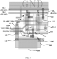
- FIG. 3 illustrates a schematic diagram corresponding to the layout on the base substrate of the display device 100 illustrated in FIG. 2 .
- the direction from the first electrode 111 of the first transistor 110 to the second electrode 112 of the first transistor 110 is referred to as a first direction D1
- the direction from the first electrode 121 of the second transistor 120 to the second electrode 122 of the second transistor 120 is referred to as a second direction D2
- the direction from the first electrode 131 of the third transistor 130 to the second electrode 132 of the third transistor 130 is referred to as a third direction D3
- the direction from the first electrode 141 of the driving transistor 140 to the second electrode 142 of the driving transistor 140 is referred to as a fourth direction D4.
- the fourth direction D4 is the horizontal direction from left to right in FIG. 3 .
- the driving transistor 140 can be arranged along the fourth direction D4 when arranging the positions of the transistors, while at least one of the first direction D1, the second direction D2, and the third direction D3 intersects with the fourth direction D4, which can make the layout of the four transistors more compact, so that the layout area occupied by the display device 100 can be reduced, and the display device 100 can more easily achieve high PPI.
- the first direction D1 and the second direction D2 can both intersect with the fourth direction D4; for another example, the first direction D1, the second direction D2, and the third direction D3 can all intersect with the fourth direction D4.
- the fourth direction D4 is the horizontal direction
- the first direction D1, the second direction D2, and the third direction D3 are all longitudinal directions in FIG. 3 that are perpendicular to the horizontal direction.
- the first direction D1 and the second direction D2 are both perpendicular to the fourth direction D4; for another example, the first direction D1, the second direction D2, and the third direction D3 are all perpendicular to the fourth direction D4.
- application of this method can make the layout of the display device 100 more compact, thereby further reducing the layout area occupied by the display device 100, and causing the display device 100 to more easily achieve high PPI.
- the first transistor 110 includes a first active region 114 extending along the first direction D1, and the first active region 114 includes the first electrode 111 of the first transistor 110, the second electrode 112 of the first transistor 110, and a channel region formed between the first electrode 111 of the first transistor 110 and the second electrode 112 of the first transistor 110.
- the second transistor 120 includes a second active region 124 extending along the second direction D2, and the second active region 124 includes the first electrode 121 of the second transistor 120, the second electrode 122 of the second transistor 120, and a channel region formed between the first electrode 121 of the second transistor 120 and the second electrode 122 of the second transistor 120.
- the third transistor 130 includes a third active region 134 extending along the third direction D3, and the third active region 134 includes the first electrode 131 of the third transistor 130, the second electrode 132 of the third transistor 130, and a channel region formed between the first electrode 131 of the third transistor 130 and the second electrode 132 of the third transistor 130.
- the driving transistor 140 includes a fourth active region 144 extending along the fourth direction D4, and the fourth active region 144 includes the first electrode 141 of the driving transistor 140, the second electrode 142 of the driving transistor 140, and a channel region formed between the first electrode 141 of the driving transistor 140 and the second electrode 142 of the driving transistor 140.
- the base substrate in the display device 100 provided by the embodiments of the present disclosure is a silicon-based base substrate
- the above-mentioned first active region 114, second active region 124, third active region 134, and fourth active region 144 are all doped regions in the silicon-based base substrate. These doped regions are obtained by, for example, an ion implantation process or an ion diffusion process.
- P-type doping may be achieved by doping boron (B)
- N-type doping may be achieved by doping phosphorus (P) or arsenic (As)
- the embodiments of the present disclosure are not limited in this aspect.
- the doping type of the first active region 114 and the doping type of the second active region 124 are opposite to each other.
- the doping type of the first active region 114 is P-type
- the doping type of the second active region 124 is N-type.
- two ends of the first active region 114 and two ends of the second active region 124 are aligned with each other in the fourth direction D4 respectively, and for example, two ends of the first active region 114 are arranged adjacent to and the second active region 124. In this way, the layout design of the display device 100 can be simplified.
- the line connecting an edge of the first active region 114 along the first direction D1 and an edge of the second active region 124 along the second direction D2 is parallel to the fourth direction D4, and the line connecting the other edge of the first active region 114 along the first direction D1 and the other edge of the second active region 124 along the second direction D2 is parallel to the fourth direction D4. In this way, the layout design of the display device 100 can be simplified.
- the driving current for the light-emitting element LE in the display device 100 is smaller by 1 to 2 orders of magnitude.
- the pixel circuit 100 provided by some embodiments of the present disclosure can eliminate or avoid the above problem by adjusting the relative relationship between the doping concentrations of the first active region 114, the second active region 124, the third active region 134, and the fourth active region 144.
- the doping concentration of the fourth active region 144 is smaller than the doping concentration of the third active region 134.
- the doping concentration of the third active region 134 is about 10 17 cm -3
- the doping concentration of the fourth active region 144 is about 10 13 cm -3
- the doping concentration of the fourth active region 144 is 4 orders of magnitude smaller than the doping concentration of the third active region 134.
- the embodiments of the present disclosure can enable the driving transistor 140 to output a smaller driving current by reducing the doping concentration of the fourth active region 144 without changing the size of the driving transistor 140 (for example, the width-to-length ratio W/L remains unchanged).
- the driving current that is outputted changes more smoothly, so that the pixel circuit adopting the driving transistor 140 drives the light-emitting element LE (for example, an OLED) to obtain better uniformity of the gray-scale value when emitting light.
- the light-emitting element LE for example, an OLED
- At least one of the doping concentration of the first active region 114 and the doping concentration of the second active region 124 is greater than the doping concentration of the third active region 134.
- the doping concentration of the first active region 114 and the doping concentration of the second active region 124 are both greater than the doping concentration of the third active region.
- the doping concentration of the first active region 114 and the doping concentration of the second active region 124 are about 10 20 cm -3 , in this case, the doping concentration of the first active region 114 and the doping concentration of the second active region 124 are both 3 orders of magnitude greater than the doping concentration of the third active region 134.
- the first transistor 110 and the second transistor 120 function as switching transistors in the pixel circuit, so they need to have good switching characteristics.
- the first active region 114 or/and the second active region 124 has a greater doping concentration, a greater driving current can be obtained and the driving current changes more quickly, thereby enabling the first transistor 110 or/and the second transistor 120 have better switching characteristics.
- the first transistor 110 is a MOS transistor with a first semiconductor type
- the second transistor, the third transistor, and the driving transistor are all MOS transistors with a second semiconductor type
- the first semiconductor type is opposite to the second semiconductor type.
- the first semiconductor type is P-type
- the second semiconductor type is N-type
- the embodiments of the present disclosure include but are not limited to this case.
- the display device 100 provided by some embodiments of the present disclosure further includes a first scan signal line SL1 for transmitting the first scan signal SCAN1 and a second scan signal line SL2 for transmitting the second scan signal SCAN2, and the first scan signal line SL1 and the second scan signal line SL2 are arranged in parallel.
- the first scan signal line SL1 is connected to the control electrode 113 of the first transistor 110 to provide the first scan signal SCAN1
- the second scan signal line SL2 is connected to the control electrode 123 of the second transistor 120 to provide the second scan signal SCAN2.
- the extension direction of the first scan signal line SL1 and the extension direction of the second scan signal line SL2 are both parallel to the fourth direction D4.
- the orthographic projection of the first scan signal line SL1 on the base substrate is parallel to the orthographic projection of the second scan signal line SL2 on the base substrate, and for example, both parallel to the fourth direction D4.
- the region where the orthographic projection of the pixel circuit on the base substrate is located is the pixel region, and the first scan signal line SL1 and the second scan signal line SL2 are juxtaposed at a side of the pixel region.
- the display device 100 provided by some embodiments of the present disclosure further includes a data line DL for transmitting the data signal DATA, and the orthographic projection of the second scan signal line SL2 on the substrate at least partially overlaps with the orthographic projection of the data line DL on the base substrate.
- the second scan signal line SL2 and the data line DL overlap with each other in a direction perpendicular to the base substrate.
- the plane where FIG. 3 is located can be regarded as the plane where the base substrate is located, and therefore being perpendicular to the base substrate is being perpendicular to the plane where FIG. 3 is located.
- the embodiment of the present disclosure can make the data line DL not occupy an extra layout area by overlapping the second scan signal line SL2 and the data line DT in the direction perpendicular to the base substrate, thereby further reducing the layout area occupied by the display device 100, and causing the display device 100 to more easily achieve high PPI.
- the display device 100 provided by some embodiments of the present disclosure further includes a first power supply voltage line VL1 for transmitting the first power supply voltage ELVDD and a light-emitting control line EL for transmitting the light-emitting control signal EN.
- the extension direction of a part of the first power supply voltage line VL1 and the extension direction of a part of the light-emitting control line EL are parallel to the fourth direction D4, and the orthographic projection of the first scan signal line SL1 on the base substrate, the orthographic projection of the second scan signal line SL2 on the base substrate, the orthographic projection of the first power supply voltage line VL1 on the base substrate, and the orthographic projection of the light-emitting control line EL on the base substrate are sequentially arranged in the direction perpendicular to the fourth direction.
- the orthographic projection of the first power supply voltage line VL1 on the base substrate is between the orthographic projection of the second scan signal line SL2 on the base substrate and the orthographic projection of the light-emitting control line EL on the base substrate, because the first power supply voltage ELVDD transmitted by the first power supply voltage line VL1 is a DC signal, and the second scan signal SCAN2 transmitted by the second scan signal line SL2 and the light-emitting control signal EN transmitted by the light-emitting control line EL are both jump signals, the above arrangement can effectively shield the mutual interference between the second scan signal SCAN2 and the light-emitting control signal EN.
- the display device 100 provided by some embodiments of the present disclosure further includes a second power supply voltage line VL2 for transmitting the second power supply voltage VDD, and the third electrode of the first transistor 110 is electrically connected to the second power supply voltage line VL2 to receive the second power supply voltage VDD.
- the second power supply voltage VDD in the embodiments of the present disclosure is a high-level voltage, for example, the second power supply voltage is at 5V.
- the first transistor 110 is a P-type MOS transistor, and the channel region of the first transistor is P-type doped.
- the third electrode, which is opposite to the control electrode (gate electrode) 113, of the first transistor 110 receives the second power supply voltage VDD.
- the second transistor 120, the third transistor 130, and the driving transistor 140 are all N-type MOS transistors, the channel regions of the second transistor 120, the third transistor 130 and the driving transistor 140 are N-type doped, and the third electrode of the second transistor 120, the third electrode of the third transistor 130, and the third electrode of the driving transistor 140 are all configured to be grounded (GND).
- the orthographic projection of the second power supply voltage line VL2 on the base substrate is between the orthographic projection of the first power supply voltage line VL1 on the base substrate and the orthographic projection of the light-emitting control line EL on the base substrate, and the extension direction of a part of the second power supply voltage line VL2 is parallel to the fourth direction D4.
- the second power supply voltage line VL2 has a bending region when extending in the fourth direction D4; in addition, the light-emitting control line EL also has a bending region when extending in the fourth direction D4, and the second power supply voltage line VL2 and the light-emitting control line EL have different bending directions. Adopting this wiring method can, for example, leave a layout space for a first transfer electrode AE1 described below.
- the first transistor 110 and the second transistor 120 are both between the second scan signal line SL2 and the light-emitting control line EL, and the first transistor 110 intersects with the first power supply voltage line VL1 and the second power supply voltage line VL2, and the second transistor 120 intersects with the first power supply voltage line VL1 and the second power supply voltage line VL2.
- the orthographic projection of the first active region 114 of the first transistor 110 on the base substrate and the orthographic projection of the second active region 124 of the second transistor 120 on the base substrate are both between the orthographic projection of the second scan signal line SL2 on the base substrate and the orthographic projection of the light-emitting control line EL on the base substrate.
- the orthographic projection of the first active region 114 of the first transistor 110 on the base substrate intersects with the orthographic projection of the first power supply voltage line VL1 on the base substrate, and the orthographic projection of the first active region 114 of the first transistor 110 on the base substrate intersects with the orthographic projection of the second power supply voltage line VL2 on the base substrate.
- the orthographic projection of the second active region 124 of the second transistor 120 on the base substrate intersects with the orthographic projection of the first power supply voltage line VL1 on the base substrate, and the orthographic projection of the second active region 124 of the second transistor 120 on the base substrate intersects with the orthographic projection of the second power supply voltage line VL2 on the base substrate.
- the display device 100 provided by some embodiments of the present disclosure further includes the first transfer electrode AE1 provided at a first side of the light-emitting control line EL, and a second transfer electrode AE2 extending from the first side of the light-emitting control line EL to a second side of the light-emitting control line EL.
- the orthographic projection of the second transfer electrode AE2 on the base substrate crosses the orthographic projection of the light-emitting control line EL on the base substrate.
- Two ends of the first transfer electrode AE1 are respectively electrically connected to the first electrode 111 of the first transistor 110 and the first electrode 121 of the second transistor 120, the first transfer electrode AE1 is electrically connected to the second transfer electrode AE2, and the second transfer electrode AE2 is electrically connected to the control electrode 143 of the driving transistor 140.
- the extension direction of the second transfer electrode AE2 is perpendicular to the extension direction of the first transfer electrode AE1 and is perpendicular to the fourth direction D4.
- the electrical level of the second transfer electrode AE2 may fluctuate greatly during operation of the pixel circuit, and the fluctuation may cause crosstalk to the first power supply voltage line VL1, and cause noises.
- the first power supply voltage line VL1 and the second transfer electrode AE2 are spaced apart by the second power supply voltage line VL2, so that the crosstalk caused by the electrical level fluctuation on the second transfer electrode AE2 on the first power supply voltage line VL1 can be reduced, and noises can be isolated.
- the display device 100 provided by some embodiments of the present disclosure extends the first active region 114 of the first transistor 110 and the second active region 124 of the second transistor 120 to leave a wiring channel for the second power supply voltage line VL2.
- the layout size of the pixel circuit (rectangular shape) provided by the embodiments of the present disclosure is approximately 4.5 ⁇ m ⁇ 2.9 ⁇ m.
- FIG. 4A-FIG. 4E respectively illustrate plan diagrams of the layout of five layers of the display device illustrated in FIG. 3 .
- FIG. 4A illustrates the first active region 114 of the first transistor 110, the second active region 124 of the second transistor 120, the third active region 134 of the third transistor 130, and the fourth active region 144 of the driving transistor 140, and the layer illustrated in FIG. 4A may be referred to as an effective display layer (AA).
- AA effective display layer
- FIG. 4B illustrates the control electrode 113 of the first transistor 110, the control electrode 123 of the second transistor 120, the control electrode 133 of the third transistor 130, and the control electrode 143 of the driving transistor 140.
- the layer illustrated in FIG. 4B may be referred to as a first conductive layer, and the first conductive layer will be described further below.
- the material of the first conductive layer may be polysilicon.
- FIG. 4C illustrates the first power supply voltage line VL1, the second power supply voltage line VL2, the light-emitting control line EL, the data line DL, the ground line GND, the first transfer electrode AE1, and the like.
- the layer illustrated in FIG. 4C may be referred to as a first metal layer (metal1).
- FIG. 4E illustrates the first scan signal line SL1 and the second scan signal line SL2, and the layer illustrated in FIG. 4E may be referred to as a third metal layer (metal3).
- the region 800 illustrated in FIG. 5 is a region where the storage capacitor CST is provided. It should be noted that, for the sake of clarity, the corresponding marks of all structures are not illustrated in FIG. 5 , and for the omitted parts, refer to the corresponding marks in FIG. 3 .
- FIG. 6 is a layout diagram of the storage capacitor CST
- FIG. 7A-FIG.7D are plan diagrams corresponding to the layout of each layer of FIG. 6
- FIG. 7E is a schematic cross-sectional diagram of the storage capacitor CST.
- FIG. 6 illustrates a structure of four layers, which is the third metal layer metal3, a fourth metal layer metal4, an auxiliary metal layer metal4', and a fifth metal layer metal5.
- a first via hole V1 and a second via hole V2 are illustrated; the first via hole V1 and the second via hole V2 will be described below in conjunction with the schematic cross-sectional diagram, and the description thereto are not repeated here for simplicity.
- FIG. 7A illustrates the third metal layer metal3, for example, the third metal layer and the layer illustrated in FIG. 4E are the same layer.
- the third metal layer metal3 includes two parts, an electrode 811 serving as the first electrode of the first capacitor C1 and an electrode 812 serving as the second electrode of the first capacitor C1.
- the electrode 811 is configured to receive the third power supply voltage AVSS; and the electrode 812 is electrically connected to the electrode 840 in the fifth metal layer metal5 through the second via hole V2, thereby achieving electrical connection with the control electrode 143 of the driving transistor 140.
- the electrode 811 includes a plurality of strip electrodes
- the electrode 812 includes a plurality of strip electrodes
- the plurality of strip electrodes of the electrode 811 and the plurality of strip electrodes of the electrode 812 are alternately arranged with each other, and the space portion between the electrode 811 and the electrode 812 forms the first capacitor C1.
- the first capacitor C1 is a part of the storage capacitor CST.
- the first capacitor C1 and the second capacitor C2 hereinafter are connected in parallel to form the storage capacitor CST.
- FIG. 7B illustrates an electrode 820 located in the fourth metal layer metal4.
- the electrode 820 is a planar electrode, and the electrode 820 serves as the first electrode of the second capacitor C2.
- FIG. 7C illustrates an electrode 830 located in the auxiliary metal layer metal4'.
- the electrode 830 is a planar electrode, and the electrode 830 serves as the second electrode of the second capacitor C2.
- FIG. 7D illustrates an electrode 840 located in the fifth metal layer metal5, and the first via hole V1 and the second via hole V2.
- FIG. 7E illustrates a schematic cross-sectional diagram of a part of the structure of the storage capacitor CST.
- the electrode 840 in the fifth metal layer metal5 is electrically connected to the electrode 830 in the auxiliary metal layer metal4' through the first via hole V1.
- the electrode 840 located in the fifth metal layer metal5 is electrically connected to the electrode 812 located in the third metal layer metal3 through the second via hole V2.
- the second via hole V2 penetrates the fourth metal layer metal4, which is not illustrated in FIG. 7E .
- the electrode 820 in the fourth metal layer metal4, the electrode 830 in the auxiliary metal layer metal4', and the space portion between the electrode 820 and the electrode 830 form the second capacitor C2.
- the first capacitor C1 described above and the second capacitor C2 are connected in parallel to form the storage capacitor CST.
- the auxiliary metal layer metal4' is provided between the fourth metal layer metal4 and the fifth metal layer metal5, so that the distance between the fourth metal layer metal4 and the auxiliary metal layer metal4' is, for example, about 1/10 of the distance between the fourth metal layer metal4 and the fifth metal layer metal5, and the capacitance value per unit area of the second capacitor C2 can be effectively increased.
- the claimed invention further provides a display device 100 including a base substrate and at least one pixel circuit provided on the base substrate.
- the pixel circuit includes a driving transistor 140, a first transistor 110, a second transistor 120, and a third transistor 130.
- the driving transistor 140 includes a control electrode 143, a first electrode 141 and a second electrode 142, and is configured to control a driving current, flowing through the first electrode 141 of the driving transistor 140 and the second electrode 142 of the driving transistor 140, for driving a light-emitting element to emit light according to a voltage of the control electrode 143 of the driving transistor 140.
- the first transistor 110 is connected to the control electrode 143 of the driving transistor 140 and is configured to write a data signal DATA to the control electrode 143 of the driving transistor 140 in response to a first scan signal SCAN1.
- the second transistor 120 is connected to the control electrode 143 of the driving transistor 140 and is configured to write the data signal DATA to the control electrode 143 of the driving transistor 140 in response to a second scan signal SCAN2.
- the third transistor 130 is connected to the first electrode 141 of the driving transistor 140 and is configured to apply a first power supply voltage ELVDD to the first electrode 141 of the driving transistor 140 in response to a light-emitting control signal EN.
- the display device 100 further includes a first scan signal line SL1 for transmitting the first scan signal SCAN1 and a second scan signal line SL2 for transmitting the second scan signal SCAN2, and a first power supply voltage line VL1 for transmitting the first power supply voltage ELVDD, and a light-emitting control line EL for transmitting the light-emitting control signal EN.
- the orthographic projection of the first scan signal line SL1 on the base substrate, the orthographic projection of the second scan signal line SL2 on the base substrate, the orthographic projection of the first power supply voltage line VL1 on the base substrate, and the orthographic projection of the light-emitting control line EL on the base substrate are sequentially arranged in a direction perpendicular to a fourth direction D4.
- a direction from the first electrode 111 of the first transistor 110 to the second electrode 112 of the first transistor 110 is a first direction D1
- a direction from a first electrode 121 of the second transistor 120 to a second electrode 122 of the second transistor 120 is a second direction D2
- a direction from a first electrode 131 of the third transistor 130 to a second electrode 132 of the third transistor 130 is a third direction D3
- a direction from the first electrode 141 of the driving transistor 140 to the second electrode 142 of the driving transistor 140 is the fourth direction D4.
- the first direction D1, the second direction D2, and the third direction D3 all intersect with the fourth direction D4, for example, the first direction D1, the second direction D2, and the third direction D3 all perpendicular to the fourth direction D4.
- At least one embodiment of the present disclosure further provides a manufacturing method of the display device 100, and the manufacturing method includes forming a pixel circuit on a base substrate.
- the pixel circuit includes a driving transistor 140, a first transistor 110, and a second transistor 120.
- the driving transistor 140 includes a control electrode 143, a first electrode 141 and a second electrode 142, and is configured to control a driving current, flowing through the first electrode 141 of the driving transistor 140 and the second electrode 142 of the driving transistor 140, for driving a light-emitting element to emit light according to a voltage of the control electrode 143 of the driving transistor 140.
- the first transistor 110 is connected to the control electrode 143 of the driving transistor 140 and is configured to write a data signal DATA to the control electrode 143 of the driving transistor 140 in response to a first scan signal SCAN1.
- the second transistor 120 is connected to the control electrode 143 of the driving transistor 140 and is configured to write the data signal DATA to the control electrode 143 of the driving transistor 140 in response to a second scan signal SCAN2.
- the direction from the first electrode 111 of the first transistor 110 to the second electrode 112 of the first transistor 110 is a first direction D1
- the direction from a first electrode 121 of the second transistor 120 to a second electrode 122 of the second transistor 120 is a second direction D2
- the direction from the first electrode 141 of the driving transistor 140 to the second electrode 142 of the driving transistor 140 is the fourth direction D4.
- the pixel circuit in the display device needs to output a higher driving current to the anode of the OLED.
- the anode voltage of the OLED needs a higher voltage V anode
- the first electrode 111 (for example, the drain electrode) of the first transistor 110 and the first electrode 121 (for example, the drain electrode) of the second transistor 120 may bear a high voltage V anode +V GS4 (V GS4 is the voltage difference between the gate electrode and the second electrode of the driving transistor 140), and a high voltage may appear between the gate electrode and the first electrode of the first transistor 110, and a high voltage may appear between the gate electrode and the first electrode of the first transistor 120.
- the first transistor 110 and the second transistor 120 in the pixel circuit may bear the high voltage, and a breakdown phenomenon may occur, which may affect the reliability and
- the claimed invention provides a structural design of a transistor that can reduce or avoid the risk of breakdown by a high voltage, so that the pixel circuit adopting the transistor cannot be easily broken by a high voltage and the high-brightness display driving of the pixel circuit can be implemented.
- the claimed invention provides a display device 100 including a base substrate and a pixel circuit provided on the base substrate.
- the pixel circuit includes a driving transistor 140, a first transistor 110, and a second transistor 120.
- the driving transistor 140 includes a control electrode 143, a first electrode 141, and a second electrode 142, and the driving transistor 140 is configured to control a driving current, flowing through the first electrode 141 of the driving transistor 140 and the second electrode 142 of the driving transistor 140, for driving a light-emitting element LE to emit light according to the voltage of the control electrode 143 of the driving transistor 140.
- a first electrode 111 of the first transistor 110 is connected to the control electrode143 of the driving transistor 140, and is configured to write a data signal DATA to the control electrode 143 of the driving transistor 140 in response to a first scan signal SCAN1.
- the second transistor 120 is connected to the control electrode 143 of the driving transistor 140, and is configured to write the data signal DATA to the control electrode 143 of the driving transistor 140 in response to a second scan signal SCAN2.
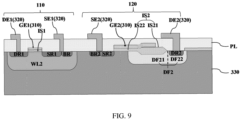
- the base substrate includes a semiconductor body 330 that can be doped, and includes a first conductive layer 310 and a second conductive layer 320 that are on the semiconductor body 330.
- the first transistor 110 includes a gate electrode GE1 in the first conductive layer 310, a second electrode SE1 and a first electrode DE1 which are both in the second conductive layer 320, a first doped region DR1 in contact with the first electrode DE1 of the first transistor 110, and a second doped region SR1 in contact with the second electrode SE1 of the first transistor 110; and the first doped region DR1 of the first transistor 110 and the second doped region SR1 of the first transistor 110 are spaced apart from each other, have the same doping type, and are both in the semiconductor body 330.
- a channel region of the first transistor 110 is between the first doped region DR1 and the second doped region SR1.
- the gate electrode GE1 of the first transistor 110 is the control electrode 113 of the first transistor 110 described above, and the following embodiments are the same and will not be repeated herein.
- the first transistor 110 further includes a drift doped region DF1 in contact with the first doped region DR1; and the drift doped region DF1 of the first transistor 110 and the second doped region SR1 of the first transistor 110 are spaced apart from each other, have the same doping type, and are both in the semiconductor body 330.
- the first transistor 110 is a P-type MOS transistor.
- the doping types of the first doped region DR1, the second doped region SR1 and the drift doped region DF1 of the first transistor 110 are all P-type doping, and the semiconductor body 330 is a bulk silicon with a doping type of P-type or a silicon-on-insulator with a doping type of P-type.
- the orthographic projection of the gate electrode GE1 of the first transistor 110 on the base substrate partially overlaps with the orthographic projection of the drift doped region DF1 of the first transistor 110 on the base substrate, and the orthographic projection of the first doped region DR1 of the first transistor 110 on the base substrate is in the orthographic projection of the drift doped region DF1 of the first transistor 110 on the base substrate.
- the doping concentration of the drift doped region DF1 of the first transistor 110 is smaller than the doping concentration of the first doped region DR1 of the first transistor 110.
- the pixel circuit in the display device 100 provided by the claimed invention provides the drift doped region DF1 in the first transistor 110 and makes the doping concentration of the drift doped region DF1 of the first transistor 110 smaller than the doping concentration of the first doped region DR1 of the first transistor 110, which can increase the breakdown voltage between the first electrode DE1 and the second electrode SE1 of the first transistor 110, so that the risk of breakdown of the first transistor 110 by a high voltage can be reduced or avoided.
- the first transistor 110 is a P-type MOS transistor.
- the drift doped region DF1 of the first transistor 110 includes a first portion DF11 and a second portion DF12.
- the orthographic projection of the second portion DF12 on the base substrate overlaps with the orthographic projection of the first doped region DR1 of the first transistor 110 on the base substrate, in this case, it can be considered that the second portion DF12 of the drift doped region DF1 of the first transistor 110 constitutes a part of the channel region and is different from other parts of the channel region.
- the first doped region DR1 of the first transistor 110 is in the drift doped region DF1 of the first transistor 110.
- the doping depth of the first doped region DR1 of the first transistor 110 in the semiconductor body 330 may be smaller than, equal to, or greater than the doping depth of the drift doped region DF1 of the first transistor 110.
- the first doped region DR1, the second doped region SR1, and the drift doped region DF1 of the first transistor 110 are in a first well WL1 in the semiconductor body 330, for example, the doping type of the first well WL1 is N-type doping.
- the orthographic projection of the gate electrode GE1 of the first transistor 110 on the base substrate is in the orthographic projection of the first well WL1 on the base substrate, and a portion, which is between the first doped region DR1 of the first transistor 110 and the second doped region SR1 of the first transistor 110, of the first well WL1 constitutes the channel region of the first transistor 110.
- FIG. 3 illustrates the region where the first well WL1 is located.
- the first transistor 110 further includes an auxiliary doped region BR, for example, the doping type of the auxiliary doped region BR of the first transistor 110 is N-type doping.
- the auxiliary doped region BR of the first transistor 110 is in contact with the second doped region SR1 of the first transistor 110, the auxiliary doped region BR of the first transistor 110 is electrically connected to the second electrode SE1 of the first transistor 110, and the orthographic projection of the auxiliary doped region BR of the first transistor 110 on the base substrate is in the orthographic projection of the first well WL1 on the base substrate.
- the auxiliary doped region BR can play an isolation role to prevent leakage.
- the base substrate in the display device 100 provided by the claimed invention further includes a first insulating layer IS1 between the semiconductor body 330 and the first conductive layer 310, and the first insulating layer IS1 can enable the gate electrode GE1 of the first transistor 110 to be insulated from the semiconductor body 330.
- the first insulating layer IS1 may be a gate insulating layer, such as a silicon oxide layer, and may be formed by a vapor deposition process, or obtained by directly oxidizing a silicon-based base substrate through a thermal oxidation process.
- the first insulating layer IS1 includes a first portion IS11 close to the first doped region DR1 of the first transistor 110 and a second portion IS12 away from the first doped region DR1 of the first transistor 110.
- the thickness of the first portion IS11 of the first insulating layer IS1 is greater than the thickness of the second portion IS12 of the first insulating layer IS1, and the thicknesses include the thickness in a direction perpendicular to the base substrate.
- the thickness of the first portion IS11 of the first insulating layer IS1 is 7-8 nm
- the thickness of the second portion IS12 of the first insulating layer IS1 is 2-3 nm.
- the risk of breakdown by a high voltage between the gate electrode GE1 of the first transistor 110 and the first electrode DE1 of the first transistor 110 can be reduced or avoided.
- the base substrate further includes a planarization insulating layer PL that covers the gate electrode GE1 of the first transistor 110, and the light-emitting element LE is above the planarization insulating layer PL.
- the planarization insulating layer PL can cover the above-mentioned pixel circuit, so that the surface of the planarization insulating layer PL is relatively flat, which is more advantageous for forming the light-emitting element LE on the planarization insulating layer PL.
- the planarization insulating layer PL may be silicon oxide, silicon oxynitride, silicon nitride, etc., and may be obtained by processes such as vapor deposition.
- the first transistor 110 adopts a structural design that can reduce or avoid the risk of breakdown by a high voltage
- the second transistor 120 adopts a structural design of a general MOS transistor.
- the second transistor 120 includes a gate electrode GE2 in the first conductive layer 310, a first electrode DE2 and a second electrode SE2 that are both in the second conductive layer 320, a first doped region DR2 in contact with the first electrode DE2 of the second transistor 120, and a second doped region SR2 in contact with the second electrode SE2 of the second transistor 120.
- the first doped region DR2 of the second transistor 120 and the second doped region SR2 of the second transistor 120 are spaced apart from each other, have the same doping type, and are both in the semiconductor body 330.
- the gate electrode GE2 of the second transistor 120 here is the control electrode 123 of the second transistor 120 described above, and the following embodiments are the same and will not be repeated herein.
- the second transistor 120 is an N-type MOS transistor, and the doping types of the first doped region DR2 and the second doped region SR2 of the second transistor 120 are both N-type doping.
- the second transistor 120 further includes an auxiliary doped region BR2, the auxiliary doped region BR2 of the second transistor 120 is in contact with the second doped region SR2 of the second transistor 120, and the auxiliary doped region BR2 of the second transistor 120 is electrically connected to the second electrode SE2 of the second transistor 120.
- the doping type of the auxiliary doped region BR2 of the second transistor 120 is opposite to the doping type of the second doped region SR2 of the second transistor 120, for example, the doping type of the auxiliary doping region BR2 of the second transistor 120 is P-type doping.
- the auxiliary doped region BR2 can play an isolation role to prevent electrical leakage.
- the first transistor 110 may also be an N-type MOS transistor, the doping type of the first doped region DR1 in the first transistor 110 is N-type, and the semiconductor body 330 is a bulk silicon with a doping type of P-type or a silicon-on-insulator with a doping type of P-type.
- the first transistor 110 may further include an auxiliary doped region, in this case, the doping type of the auxiliary doped region of the first transistor 110 is P-type.
- the auxiliary doped region of the first transistor 110 is in contact with the second doped region SR1 of the first transistor 110, and the auxiliary doped region is electrically connected to the second electrode SE1 of the first transistor 110.
- the second transistor 120 adopts a structural design that can reduce or avoid the risk of breakdown by a high voltage
- the first transistor 110 adopts a structural design of a general MOS transistor.
- the second transistor 120 includes a gate electrode GE2 in the first conductive layer 310, a first electrode DE2 and a second electrode SE2 that are both in the second conductive layer 320, a first doped region DR2 in contact with the first electrode DE2 of the second transistor 120, and a second doped region SR2 in contact with the second electrode SE2 of the second transistor 120.
- the first doped region DR2 of the second transistor 120 and the second doped region SR2 of the second transistor 120 are spaced apart from each other, have the same doping type, and are both in the semiconductor body 330.
- the second transistor 120 further includes a drift doped region DF2 in contact with the first doped region DR2; and the drift doped region DF2 of the second transistor 120 and the second doped region SR2 of the second transistor 120 are spaced apart from each other, have the same doping type, and are both in the semiconductor body 330.
- the second transistor 120 is a P-type MOS transistor.
- the doping types of the first doped region DR2, the second doped region SR2, and the drift doped region DF2 of the second transistor 120 are all N-type doping, and the semiconductor body 330 is a bulk silicon with a doping type of P-type or a silicon-on-insulator with a doping type of P-type.
- the orthographic projection of the gate electrode GE2 of the second transistor 120 on the base substrate partially overlaps with the orthographic projection of the drift doped region DF2 of the second transistor 120 on the base substrate, and the orthographic projection of the first doped region DR2 of the second transistor 120 on the base substrate is in the orthographic projection of the drift doped region DF2 of the second transistor 120 on the base substrate.
- the doping concentration of the drift doped region DF2 of the second transistor 120 is smaller than the doping concentration of the first doped region DR2 of the second transistor 120.
- the pixel circuit in the display device 100 provided by the embodiments of the present disclosure provides the drift doped region DF2 in the second transistor 120 and makes the doping concentration of the drift doped region DF2 of the second transistor 120 smaller than the doping concentration of the first doped region DR2 of the second transistor 120, which can increase the breakdown voltage between the first electrode DE2 and the second electrode SE2 of the second transistor 120, so that the risk of breakdown of the second transistor 120 by a high voltage can be reduced or avoided. As illustrated in FIG.
- the drift doped region DF2 of the second transistor 120 includes a first portion DF21 and a second portion DF22, and the orthographic projection of the second portion DF22 on the base substrate overlaps with the orthographic projections of the first doped region DR2 of the second transistor 120 on the base substrate.
- the first doped region DR2 of the second transistor 120 is in the drift doped region DF2 of the second transistor 120.
- the second transistor 120 further includes an auxiliary doped region BR2, and for example, the doping type of the auxiliary doping region BR2 of the second transistor 120 is P-type doping.
- the auxiliary doped region BR2 of the second transistor 120 is in contact with the second doped region SR2 of the second transistor 120, and the auxiliary doped region BR2 of the second transistor 120 is electrically connected to the second electrode SE2 of the second transistor 120.
- the auxiliary doped region BR2 can play an isolation role to prevent leakage.
- the base substrate in the display device 100 further includes a second insulating layer IS2 between the semiconductor body 330 and the first conductive layer 310, and the second insulating layer IS1 can enable the gate electrode GE2 of the second transistor 120 to be insulated from the semiconductor body 330.
- the second insulating layer IS2 may be a gate insulating layer, such as a silicon oxide layer, and may be formed by a vapor deposition process, or obtained by directly oxidizing a silicon-based base substrate through a thermal oxidation process.
- the second insulating layer IS2 includes a first portion IS21 close to the first doped region DR2 of the second transistor 120 and a second portion IS22 away from the first doped region DR2 of the second transistor 120.
- the thickness of the first portion IS21 of the second insulating layer IS2 is greater than the thickness of the second portion IS22 of the second insulating layer IS2, and the thicknesses include the thickness in the direction perpendicular to the base substrate.
- the thickness of the second portion IS21 of the second insulating layer IS2 is 7-8 nm, and the thickness of the second portion IS22 of the second insulating layer IS2 is 2-3 nm.
- the risk of breakdown by a high voltage between the gate electrode GE2 of the second transistor 120 and the first electrode DE2 of the second transistor 120 can be reduced or avoided.
- the base substrate further includes a planarization insulating layer PL that covers the gate electrode GE2 of the second transistor 120 and the light-emitting element LE is above the planarization insulating layer PL.
- the planarization insulating layer PL can cover the above-mentioned pixel circuit, so that the surface of the planarization insulating layer PL is relatively flat, which is more advantageous for forming the light-emitting element LE on the planarization insulating layer PL.
- the planarization insulating layer PL may be silicon oxide, silicon oxynitride, silicon nitride, etc., and may be obtained by processes such as vapor deposition.
- the second transistor 120 adopts a structural design that can reduce or avoid the risk of breakdown by a high voltage
- the first transistor 110 adopts a structural design of a general MOS transistor.
- the first transistor 110 includes a gate electrode GE1 in the first conductive layer 310, a first electrode DE1 and a second electrode SE1 that are both in the second conductive layer 320, a first doped region DR1 in contact with the first electrode DE1 of the first transistor 110, and a second doped region SR1 in contact with the second electrode SE1 of the first transistor 110.
- the first doped region DR1 of the first transistor 110 and the second doped region SR1 of the first transistor 110 are spaced apart from each other, have the same doping type, and are both in the semiconductor body 330.
- the first transistor 110 is a P-type MOS transistor, and the doping types of the first doped region DR1 and the second doped region SR1 of the first transistor 110 are both P-type doping.
- the first doped region DR1 and the second doped region SR1 of the first transistor 110 are in a second well WL2 in the semiconductor body 330, for example, the doping type of the second well WL2 is N-type doping.
- the orthographic projection of the gate electrode GE1 of the first transistor 110 on the base substrate is in the orthographic projection of the second well WL2 on the base substrate, and a portion, which is between the first doped region DR1 of the first transistor 110 and the second doped region SR1 of the first transistor 110, of the second well WL2 constitutes the channel region of the first transistor 110.
- the first transistor 110 further includes an auxiliary doped region BR, for example, the doping type of the auxiliary doped region BR of the first transistor 110 is N-type doping.
- the auxiliary doped region BR of the first transistor 110 is in contact with the second doped region SR1 of the first transistor 110, the auxiliary doped region BR of the first transistor 110 is electrically connected to the second electrode SE1 of the first transistor 110, and the orthographic projection of the auxiliary doped region BR of the first transistor 110 on the base substrate is in the orthographic projection of the second well WL2 on the base substrate.
- the auxiliary doped region BR can play an isolation role to prevent leakage.
- both the first transistor 110 and the second transistor 120 adopt a structural design that can reduce or avoid the risk of breakdown by a high voltage.
- first transistor 110 and the second transistor 120 adopt a structural design that can reduce or avoid the risk of breakdown by a high voltage.
- both the first transistor 110 and the second transistor 120 adopt structural designs that can reduce or avoid the risk of breakdown by a high voltage, the risk of breakdown by a high voltage can be reduced or avoided, thereby improving the reliability and stability of the display device.
- the base substrate is a P-type silicon base substrate
- the first transistor 110 is a P-type MOS transistor
- the second transistor 120, the third transistor 130, and the driving transistor 140 are all N-type MOS transistors.
- At least one embodiment of the present disclosure further provides a manufacturing method of the display device 100.
- the manufacturing method includes forming a pixel circuit on a base substrate.
- the pixel circuit includes a driving transistor 140, a first transistor 110, and a second transistor 120.
- the driving transistor 140 includes a control electrode 143, a first electrode 141 and a second electrode 142, and is configured to control a driving current, flowing through the first electrode 141 of the driving transistor 140 and the second electrode 142 of the driving transistor 140, for driving a light-emitting element to emit light according to a voltage of the control electrode 143 of the driving transistor 140.
- the first transistor 110 is connected to the control electrode 143 of the driving transistor 140 and is configured to write a data signal DATA to the control electrode 143 of the driving transistor 140 in response to a first scan signal SCAN1.
- the second transistor 120 is connected to the control electrode 143 of the driving transistor 140 and is configured to write the data signal DATA to the control electrode 143 of the driving transistor 140 in response to a second scan signal SCAN2.
- the above base substrate further includes a semiconductor body 330 that can be doped, and the above manufacturing method further includes: forming a first conductive layer 310 and a second conductive layer 320 of the base substrate on the semiconductor body 330.
- the first transistor 110 includes a gate electrode GE1 in the first conductive layer 310, and a first electrode DE1 and a second electrode SE1 that are in the second conductive layer 320.
- the above manufacturing method further includes: forming a first doped region DR1 of the first transistor 110 in contact with the first electrode DE1 of the first transistor 110 and a second doped region SR1 of the first transistor 110 in contact with the second electrode SE1 of the first transistor 110 in the semiconductor body 330.
- the first doped region DR1 of the first transistor 110 and the second doped region SR1 of the first transistor 110 are spaced apart from each other, have the same doping type, and are both in the semiconductor body 330.
- the above manufacturing method further includes: forming a drift doped region DF1 of the first transistor 110 with the same doping type as the second doped region SR1 of the first transistor 110 in the semiconductor body 330.
- the drift doped region DF1 of the first transistor 110 is in the semiconductor body 330 and spaced apart from the second doped region SR1 of the first transistor 110, the orthographic projection of the gate electrode GE1 of the first transistor 110 on the base substrate partially overlaps with the orthographic projection of the drift doped region DF1 of the first transistor 110 on the base substrate, the orthographic projection of the first doped region DR1 of the first transistor 110 on the base substrate is in the orthographic projection of the drift doped region DF1 of the first transistor 110 on the base substrate, and the doping concentration of the drift doped region DF1 of the first transistor 110 is smaller than the doping concentration of the first doped region DR1 of the first transistor 110.
- the above manufacturing method further includes: forming a first insulating layer IS1 of the base substrate between the semiconductor body 330 and the first conductive layer 310.
- the first insulating layer IS1 includes a first portion IS11 close to the first doped region DR1 of the first transistor 110, and includes a second portion IS12 away from the first doped region DR1 of the first transistor 110.
- the thickness of the first portion IS11 of the first insulating layer IS1 is greater than the thickness of the second portion IS12 of the first insulating layer IS1, and the thicknesses include the thickness in the direction perpendicular to the base substrate.
- At least one embodiment of the present disclosure further provides a manufacturing method of the display device 100.
- the manufacturing method includes forming a pixel circuit on a base substrate.
- the pixel circuit includes a driving transistor 140, a first transistor 110, and a second transistor 120.
- the driving transistor 140 includes a control electrode 143, a first electrode 141 and a second electrode 142, and is configured to control a driving current, flowing through the first electrode 141 of the driving transistor 140 and the second electrode 142 of the driving transistor 140, for driving a light-emitting element to emit light according to a voltage of the control electrode 143 of the driving transistor 140.
- the first transistor 110 is connected to the control electrode 143 of the driving transistor 140 and is configured to write a data signal DATA to the control electrode 143 of the driving transistor 140 in response to a first scan signal SCAN1.
- the second transistor 120 is connected to the control electrode 143 of the driving transistor 140 and is configured to write the data signal DATA to the control electrode 143 of the driving transistor 140 in response to a second scan signal SCAN2.
- the first transistor 110 includes a first active region 114
- the second transistor 120 includes a second active region 124
- the driving transistor 140 includes a fourth active region 144.
- the above manufacturing method further includes: doping the first active region 114, the second active region 124, and the fourth active region 144 so that at least one of the doping concentration of the first active region 114 and the doping concentration of the second active region 124 is greater than the doping concentration of the fourth active region 144.
- the above pixel circuit further includes a third transistor 130, the third transistor 130 is connected to the first electrode 141 of the driving transistor 140 and is configured to apply the first power supply voltage ELVDD to the first electrode 141 of the driving transistor 140 in response to the light-emitting control signal EN, and the third transistor 130 includes a third active region 134.
- the above manufacturing method further includes: doping the third active region 134 so that the doping concentration of the fourth active region 144 is smaller than the doping concentration of the third active region 134.
- the manufacturing method of the display device 100 provided by the embodiment of the present disclosure will be described below by taking the embodiment illustrated in FIG. 8 as an example.
- the semiconductor body 330 is first provided, and then N-type doping is performed in the semiconductor body 330 to form the first well WL1; then, P-type doping is performed in the first well WL1 to form the drift doped region DF1 of the first transistor 110; then, P-type doping is performed in the drift doped region DF1 of the first transistor 110 to form the first doped region DR1 of the first transistor 110, and the doping concentration of the first doped region DR1 of the first transistor 110 is greater than the doping concentration of the drift doped region DF1 of the first transistor 110; meanwhile, P-type doping is performed in the first well WL1 to form the second doped region SR1 of the first transistor 110, and N-type doping is performed to form the auxiliary doped region BR of the first transistor 110.
- the first insulating layer IS1 is formed on the semiconductor body 330, and the thickness of the first portion IS11 of the first insulating layer IS1 is greater than the thickness of the second portion IS12 of the first insulating layer IS1; then, the first conductive layer 310 is formed on the first insulating layer IS1, and the first conductive layer 310 includes the gate electrode GE1 of the first transistor 110.
- a planarization insulating layer PL is formed to cover the gate electrode GE1 of the first transistor 110; then, the via hole is formed in the planarization insulating layer PL to expose the first doped region DR1 of the first transistor 110, the second doped region SR1 of the first transistor 110, and the auxiliary doped region BR of the first transistor 110.
- the second conductive layer 320 includes the first electrode DE1 of the first transistor 110 electrically connected to the first doped region DR1 of the first transistor 110 through the via hole in the planarization insulating layer PL described above, and the second electrode SE1 of the first transistor 110 electrically connected to the second doped region SR1 of the first transistor 110 through the via hole in the planarization insulating layer PL described above.
- the manufacturing method of the second transistor 120 is similar to the above and is not repeated here for simplicity.
- At least one embodiment of the present disclosure further provides a display device 100, as illustrated in FIG. 11 , for example, the display device 100 includes a display panel including a plurality of pixel units PU arranged in an array in the display region 300.
- the display device 100 includes a display panel including a plurality of pixel units PU arranged in an array in the display region 300.
- the plurality of pixel units PU may adopt the pixel circuit in any display device 100 provided by the embodiments of the present disclosure.
- the display device 100 further includes a driving circuit 200 manufactured in the base substrate, and the driving circuit 200 is configured to provide the first scan signal SCAN1, the second scan signal SCAN2, and the light-emitting control signal EN to the pixel circuits in the plurality of pixel units PU in the display device 100.
- the driving circuit 200 is provided in a peripheral region 400 surrounding the display region 300.
- the display device 100 may be an electronic paper, a mobile phone, a tablet computer, a television, a display, a notebook computer, a digital photo frame, a navigator and other products or members having display function.
Landscapes
- Engineering & Computer Science (AREA)
- Microelectronics & Electronic Packaging (AREA)
- Physics & Mathematics (AREA)
- Geometry (AREA)
- Manufacturing & Machinery (AREA)
- Computer Hardware Design (AREA)
- General Physics & Mathematics (AREA)
- Theoretical Computer Science (AREA)
- Devices For Indicating Variable Information By Combining Individual Elements (AREA)
- Electroluminescent Light Sources (AREA)
Claims (13)
- Anzeigevorrichtung (100), umfassend ein Basissubstrat und mindestens eine auf dem Basissubstrat vorgesehene Pixelschaltung wobei:die Pixelschaltung einen Treibertransistor (140), einen ersten Transistor (110) und einen zweiten Transistor (120) umfasst;der Treibertransistor (140) eine Steuerelektrode (143), eine erste Elektrode (141) und eine zweite Elektrode (142) umfasst und konfiguriert ist, um einen durch die erste Elektrode (141) des Treibertransistors (140) und die zweite Elektrode (142) des Treibertransistors (140) fließenden Treiberstrom zu steuern, um ein lichtemittierendes Element (LE) anzusteuern, dass es gemäß einer Spannung der Steuerelektrode (143) des Treibertransistors (140) Licht emittiert;der erste Transistor (110) eine erste Elektrode (111), eine Steuerelektrode (113) und eine zweite Elektrode (112) umfasst, die erste Elektrode (111) des ersten Transistors (110) an die Steuerelektrode (143) des Treibertransistors (140) angeschlossen ist und konfiguriert ist, um in Antwort auf ein erstes Abtastsignal (SCAN1) ein Datensignal (DATA) an die Steuerelektrode (143) des Treibertransistors (140) zu schreiben, und die Steuerelektrode (113) des ersten Transistors (110) konfiguriert ist, um das erste Abtastsignal (SCAN1) zu empfangen;der zweite Transistor (120) eine erste Elektrode (121), eine Steuerelektrode (123) und eine zweite Elektrode (122) umfasst, die erste Elektrode (121) des zweiten Transistors (120) an die Steuerelektrode (143) des Treibertransistors (140) angeschlossen ist und konfiguriert ist, um das Datensignal (DATA) in Antwort auf ein zweites Abtastsignal (SCAN2) an die Steuerelektrode (143) des Treibertransistors (140) zu schreiben, und die Steuerelektrode (123) des zweiten Transistors (120) konfiguriert ist, um das zweite Abtastsignal (SCAN2) zu empfangen;das Basissubstrat einen Halbleiterkörper (330), der dotiert werden kann, und eine erste leitfähige Schicht (310) und eine zweite leitfähige Schicht (320) die sich auf dem Halbleiterkörper (330) befindet, umfasst die erste leitfähige Schicht (310) eine GateElektrode (GE1) des ersten Transistors (110) umfasst, und die zweite leitfähige Schicht (320) die erste Elektrode (111) und die zweite Elektrode (112) des ersten Transistors (110) umfasst;der erste Transistor (110) außerdem eine erste dotierte Region (DR1) in Kontakt mit der ersten Elektrode (111) des ersten Transistors (110) und eine zweite dotierte Region (SR1) in Kontakt mit der zweiten Elektrode (112) des ersten Transistors (110) umfasst, und die erste dotierte Region (DR1) des ersten Transistors (110) und die zweite dotierte Region (SR1) des ersten Transistors (110) voneinander beabstandet sind, einen gleichen Dotierungstyp haben und beide in dem Halbleiterkörper (330) sind;der erste Transistor (110) außerdem eine driftdotierte Region (DF1) in Kontakt mit der ersten dotierten Region (DR1) umfasst, und di driftdotierte Region (DF1) des ersten Transistors (110) und die zweite dotierte Region (SR1) des ersten Transistors (110) voneinander beabstandet sind, einen gleichen Dotierungstyp haben und beide in dem Halbleiterkörper (330) sind;eine orthogonale Projektion der Gate-Elektrode (GE1) des ersten Transistors (110) auf das Basissubstrat teilweise mit einer orthogonalen Projektion der driftdotierten Region (DF1) des ersten Transistors (110) auf das Basissubstrat überlappt, und eine orthogonale Projektion der ersten dotierten Region (DR1) des ersten Transistors (110) auf das Basissubstrat in der orthogonalen Projektion der driftdotierten Region (DF1) des ersten Transistors (110) auf das Basissubstrat liegt; undeine Dotierungskonzentration der driftdotierten Region (DF1) des ersten Transistors (110) kleiner ist als eine Dotierungskonzentration der ersten dotierten Region (DR1) des ersten Transistors (110);das Basissubstrat außerdem eine erste Isolierschicht (IS1) zwischen dem Halbleiterkörper (330) und der ersten leitfähigen Schicht (310) umfasst; unddie erste Isolierschicht (IS1) einen ersten Abschnitt (IS11) nahe der ersten dotierten Region (DR1) des ersten Transistors (110) umfasst und einen zweiten Abschnitt (IS12) entfernt von der ersten dotierten Region (DR1) des ersten Transistors (110) umfasst;eine erste Dicke des ersten Abschnitts (IS11) der ersten Isolierschicht (IS1) größer ist als eine zweite Dicke des zweiten Abschnitts (IS12) der ersten Isolierschicht (IS1), und die erste Dicke und die zweite Dicke in einer Richtung senkrecht zum Basissubstrat sind.
- Anzeigevorrichtung (100) gemäß Anspruch 1, wobei:der erste Transistor (110) ein MOS-Transistor vom P-Typ ist und ein Dotierungstyp der ersten dotierten Region (DR1) des ersten Transistors (110) vom P-Typ ist;der Halbleiterkörper (330) ein Bulk-Silizium mit einem Dotierungstyp vom P-Typ oder ein Silizium-auf-Isolator mit einem Dotierungstyp vom P-Typ ist;die erste dotierte Region (DR1) des ersten Transistors (110), die zweite dotierte Region (SR1) des ersten Transistors (110) und die driftdotierte Region (DF1) des ersten Transistors (110) in einer ersten Wanne (WL1) in dem Halbleiterkörper (330) sind, und ein Dotierungstyp der ersten Wanne (WL1) vom N-Typ ist;die orthogonale Projektion der Gate-Elektrode (GE1) des ersten Transistors (110) auf das Basissubstrat in einer orthogonalen Projektion der ersten Wanne (WL1) auf das Basissubstrat ist, und ein Abschnitt, der zwischen der ersten dotierten Region (DR1) des ersten Transistors (110) und der zweiten dotierten Region (SR1) des ersten Transistors (110) ist, der ersten Wanne (WL1) eine Kanalregion des ersten Transistors (110) bildet;der erste Transistor (110) außerdem eine dotierte Hilfsregion (BR) umfasst, ein Dotierungstyp der dotierten Hilfsregion (BR) des ersten Transistors (110) vom N-Typ ist, die dotierte Hilfsregion (BR) des ersten Transistors (110) in Kontakt mit der zweiten dotierten Region (SR1) des ersten Transistors (110) ist, die dotierte Hilfsregion (BR) des ersten Transistors (110) elektrisch an die zweite Elektrode (SE1) des ersten Transistors (110) angeschlossen ist; undeine orthogonale Projektion der dotierten Hilfsregion (BR) des ersten Transistors (110) auf das Basissubstrat in der orthogonalen Projektion der ersten Wanne (WL1) auf das Basissubstrat liegt.
- Anzeigevorrichtung (100) gemäß Anspruch 1 oder 2, wobei:der erste Transistor (110) ein MOS-Transistor vom N-Typ ist und ein Dotierungstyp der ersten dotierten Region (DR1) des ersten Transistors (110) vom N-Typ ist;der Halbleiterkörper (330) ein Bulk-Silizium mit einem Dotierungstyp vom P-Typ oder ein Silizium-auf-Isolator mit einem Dotierungstyp vom P-Typ ist; undder erste Transistor (110) außerdem eine dotierte Hilfsregion umfasst, ein Dotierungstyp der dotierten Hilfsregion des ersten Transistors (110) vom P-Typ ist, die dotierte Hilfsregion des ersten Transistors (110) in Kontakt mit der zweiten dotierten Region (SR1) des ersten Transistors (110) ist, und die dotierte Hilfsregion elektrisch an die zweite Elektrode (112) des ersten Transistors (110) angeschlossen ist.
- Anzeigevorrichtung (100) gemäß einem der Ansprüche 1 bis 3, wobei:das Basissubstrat außerdem eine Planarisierungsisolierschicht (PL) umfasst, die Planarisierungsisolierschicht (PL) die Gate-Elektrode (GE1) des ersten Transistors (110) bedeckt und das lichtemittierende Element (LE) über der Planarisierungsisolierschicht (PL) ist; undder zweite Transistor (120) eine erste dotierte Region (DR2) in Kontakt mit der ersten Elektrode (DE2) des zweiten Transistors (120) umfasst und eine zweite dotierte Region (SR2) in Kontakt mit einer zweiten Elektrode (SE2) des zweiten Transistors (120) umfasst, und die erste dotierte Region (DR2) des zweiten Transistors (120) und die zweite dotierte Region (SR2) des zweiten Transistors (120) voneinander beabstandet sind, einen selben Dotierungstyp aufweisen und beide in dem Halbleiterkörper (330) sind.
- Anzeigevorrichtung (100) gemäß Anspruch 4, wobei:der zweite Transistor (120) außerdem eine dotierte Hilfsregion (BR2) umfasst, die dotierte Hilfsregion (BR2) des zweiten Transistors (120) in Kontakt mit der zweiten dotierten Region (SR2) des zweiten Transistors (120) ist, die dotierte Hilfsregion (BR2) des zweiten Transistors (120) elektrisch an die zweite Elektrode (SE2) des zweiten Transistors (120) angeschlossen ist;ein Dotierungstyp der dotierten Hilfsregion (BR2) des zweiten Transistors (120) entgegengesetzt zu einem Dotierungstyp der zweiten dotierten Region (SR2) des zweiten Transistors (120) ist; undein Dotierungstyp des ersten dotierten Region (DR1) des ersten Transistors (110) entgegengesetzt zu einem Dotierungstyp der ersten dotierten Region (DR2) des zweiten Transistors (120) ist.
- Anzeigevorrichtung (100) gemäß Anspruch 1, wobei:der erste Transistor (110) ein MOS-Transistor vom P-Typ ist, ein Dotierungstyp der ersten dotierten Region (DR1) des ersten Transistors (110) ein P-Typ ist, der zweite Transistor (120) ein MOS-Transistor vom N-Typ ist und ein Dotierungstyp einer ersten dotierten Region (DR2) des zweiten Transistors (120) ein N-Typ ist;der Halbleiterkörper (330) ein Bulk-Silizium mit einem Dotierungstyp vom P-Typ oder ein Silizium-auf-Isolator mit einem Dotierungstyp vom P-Typ ist; undder zweite Transistor (120) die erste dotierte Region (DR2) in Kontakt mit der ersten Elektrode (DE2) des zweiten Transistors (120) umfasst und eine zweite dotierte Region (SR2) in Kontakt mit einer zweiten Elektrode (SE2) des zweiten Transistors (120) umfasst, und die erste dotierte Region (DR2) des zweiten Transistors (120) und die zweite dotierte Region (SR2) des zweiten Transistors (120) voneinander beabstandet sind, einen gleichen Dotierungstyp aufweisen und beide in dem Halbleiterkörper (330) sind.
- Anzeigevorrichtung (100) gemäß Anspruch 6, wobei:der zweite Transistor (120 außerdem eine driftdotierte Region (DF2) in Kontakt mit der ersten dotierten Region (DR2) des zweiten Transistors (120) umfasst, und die driftdotierte Region (DF2) des zweiten Transistors (120) und die zweite dotierte Region (SR2) des zweiten Transistors (120) voneinander beabstandet sind, einen selben Dotierungstyp aufweisen und beide in dem Halbleiterkörper (330) sind;eine orthogonale Projektion einer Gate-Elektrode (GE2) des zweiten Transistors (120) auf das Basissubstrat teilweise mit einer orthogonalen Projektion der driftdotierten Region (DF2) des zweiten Transistors (120) auf das Basissubstrat überlappt, und eine orthogonale Projektion der ersten dotierten Region (DR2) des zweiten Transistors (120) auf das Basissubstrat in einer orthogonalen Projektion der driftdotierten Region (DF2) des zweiten Transistors (120) auf das Basissubstrat ist; undeine Dotierungskonzentration der driftdotierten Region (DF2) des zweiten Transistors (120) kleiner ist als eine Dotierungskonzentration der ersten dotierten Region (DR2) des zweiten Transistors (120).
- Anzeigevorrichtung (100) gemäß Anspruch 7, wobei:die erste dotierte Region (DR1) des ersten Transistors (110), die zweite dotierte Region (SR1) des ersten Transistors (110) und die driftdotierte Region (DF1) des ersten Transistors (110) in einer ersten Wanne (WL1) in dem Halbleiterkörper (330) sind, und ein Dotierungstyp der ersten Wanne vom N-Typ ist; unddie orthogonale Projektion der Gate-Elektrode (GE1) des ersten Transistors (110) auf das Basissubstrat in einer orthogonalen Projektion der ersten Wanne (WL1) auf das Basissubstrat ist, und ein Abschnitt, der zwischen der ersten dotierten Region (DR1) des ersten Transistors (110) und der zweiten dotierten Region (SR1) des ersten Transistors (110) ist, der ersten Wanne (WL1) eine Kanalregion des ersten Transistors (110) bildet.
- Anzeigevorrichtung (100) gemäß Anspruch 8, wobei:der erste Transistor (110) außerdem eine dotierte Hilfsregion (BR) umfasst, ein Dotierungstyp der dotierten Hilfsregion (BR) des ersten Transistors (110) vom N-Typ ist, die dotierte Hilfsregion (BR) des ersten Transistors (110) in Kontakt mit der zweiten dotierten Region (SR1) des ersten Transistors (110) ist, die dotierte Hilfsregion (BR) des ersten Transistors (110) elektrisch an die zweite Elektrode (SE1) des ersten Transistors (110) angeschlossen ist, undeine orthogonale Projektion der dotierten Hilfsregion (BR) des ersten Transistors (110) auf das Basissubstrat in der orthogonalen Projektion der ersten Wanne (WL1) auf das Basissubstrat ist; undder zweite Transistor (120) außerdem eine dotierte Hilfsregion (BR2) aufweist, ein Dotierungstyp der dotierten Hilfsregion (BR2) des zweiten Transistors (120) vom P-Typ ist, die dotierte Hilfsregion (BR2) des zweiten Transistors (120) in Kontakt mit der zweiten dotierten Region (SR2) des zweiten Transistors (120) ist, und die dotierte Hilfsregion (BR2) des zweiten Transistors (120) elektrisch an die zweite Elektrode (SE2) des zweiten Transistors (120) angeschlossen ist.
- Anzeigevorrichtung (100) gemäß einem der Ansprüche 6 bis 9, wobei:das Basissubstrat außerdem eine erste Isolierschicht (IS1) und eine zweite Isolierschicht (IS2) umfasst, die zwischen dem Halbleiterkörper (330) und der ersten leitfähigen Schicht (310) sind;die erste Isolierschicht (IS1) einen ersten Abschnitt (IS11) nahe der ersten dotierten Region (DR1) des ersten Transistors (110) und einen zweiten Abschnitt (IS12) entfernt von der ersten dotierten Region (DR1) des ersten Transistors (110) umfasst;die zweite Isolierschicht (IS2) einen ersten Abschnitt (IS21) nahe der ersten dotierten Region (DR2) des zweiten Transistors (120) und einen zweiten Abschnitt (IS22) entfernt von der ersten dotierten Region (DR2) des zweiten Transistors (120) umfasst;eine erste Dicke des ersten Abschnitts (IS11) der ersten Isolierschicht (IS1) größer ist als eine zweite Dicke des zweiten Abschnitts (IS12) der ersten Isolierschicht (IS1), eine dritte Dicke des ersten Abschnitts (IS21) der zweiten Isolierschicht (IS2) größer ist als eine vierte Dicke des zweiten Abschnitts (IS22) der zweiten Isolierschicht (IS2), unddie erste Dicke, die zweite Dicke, die dritte Dicke und die vierte Dicke in einer Richtung senkrecht zu dem Basissubstrat sind.
- Anzeigevorrichtung (100) gemäß einem der Ansprüche 1 bis 10, wobei:
die Pixelschaltung außerdem einen dritten Transistor (130) umfasst und der dritte Transistor (130) an die erste Elektrode (141) des Treibertransistors (140) angeschlossen ist und konfiguriert ist, um eine erste Energieversorgungsspannung (ELVDD) an die erste Elektrode (141) des Treibertransistors (140) in Antwort auf ein Lichtemissionssteuersignal (EN) anzulegen. - Anzeigevorrichtung (100) gemäß Anspruch 11, wobei:das Basissubstrat ein P-Typ-Siliziumbasissubstrat ist, der erste Transistor (110) ein P-Typ-MOS-Transistor ist und der zweite Transistor (120), der dritte Transistor (130) und der Treibertransistor (140) alle N-Typ-MOS-Transistoren sind; unddie Anzeigevorrichtung (100) außerdem eine Ansteuerungsschaltung (200) auf dem Basissubstrat umfasst, wobei die Ansteuerungsschaltung (200) konfiguriert ist, das erste Abtastsignal (SCAN1), das zweite Abtastsignal (SCAN2) und das Lichtemissionssteuersignal (EN) an die mindestens eine Pixelschaltung in der Anzeigevorrichtung (100) zu liefern.
- Verfahren zur Herstellung einer Anzeigevorrichtung (100), umfassend:Bilden einer Pixelschaltung auf einem Basissubstrat, wobeidie Pixelschaltung einen Treibertransistor (140), einen ersten Transistor (110) und einen zweiten Transistor (120) umfasst;der Treibertransistor (140) eine Steuerelektrode (143), eine erste Elektrode (141) und eine zweite Elektrode (142) umfasst und konfiguriert ist, um einen durch die erste Elektrode (141) des Treibertransistors (140) und die zweite Elektrode (142) des Treibertransistors (140) fließenden Treiberstrom zu steuern, um ein lichtemittierendes Element (LE) anzusteuern, so dass es entsprechend einer Spannung der Steuerelektrode (143) des Treibertransistors (140) Licht emittiert;der erste Transistor (110) eine erste Elektrode (111), eine Steuerelektrode (113) und eine zweite Elektrode (122) umfasst, die erste Elektrode (111) des ersten Transistors (110) an die Steuerelektrode (143) des Treibertransistors (140) angeschlossen ist und konfiguriert ist, um in Antwort auf ein erstes Abtastsignal (SCAN1) ein Datensignal (DATA) an die Steuerelektrode (143) des Treibertransistors (140) zu schreiben, und die Steuerelektrode (113) des ersten Transistors (110)konfiguriert ist, um das erste Abtastsignal (SCAN1) zu empfangen; der zweite Transistor (120) eine erste Elektrode (121), eine Steuerelektrode (123) und eine zweite Elektrode (112) umfasst, die erste Elektrode (121) des zweiten Transistors (120) an die Steuerelektrode (143) des Treibertransistors (140) angeschlossen ist und konfiguriert ist, um das Datensignal (DATA) in Antwort auf ein zweites Abtastsignal (SCAN2) an die Steuerelektrode (143) des Treibertransistors (140) zu schreiben, und die Steuerelektrode (123) des zweiten Transistors (120) konfiguriert ist, um das zweite Abtastsignal (SCAN2) zu empfangen;das Basissubstrat einen Halbleiterkörper (330), der dotiert werden kann, umfasst;das Herstellungsverfahren außerdem umfasst:Bilden einer ersten leitfähigen Schicht (310) und einer zweiten leitfähigen Schicht (320) des Basissubstrats auf dem Halbleiterkörper (330), wobei der erste Transistor (110) eine Gate-Elektrode (GE1) in der ersten leitfähigen Schicht (310) und eine erste Elektrode (111) und eine zweite Elektrode (112), die in der zweiten leitenden Schicht (320) sind, umfasst;Bilden einer ersten dotierten Region (DR1) des ersten Transistors (110) in Kontakt mit der ersten Elektrode (111) des ersten Transistors (110) und einer zweiten dotierten Region (DR1) des ersten Transistors (110) in Kontakt mit der zweiten Elektrode (112) des ersten Transistors (110) in dem Halbleiterkörper (330), wobei die erste dotierte Region (DR1) des ersten Transistors (110) und die zweite dotierte Region (SR1) des ersten Transistors (110) voneinander beabstandet sind, einen gleichen Dotierungstyp aufweisen und beide in dem Halbleiterkörper (330) sind; undBilden einer driftdotierten Region (DF1) des ersten Transistors (110) mit demselben Dotierungstyp wie die zweite dotierte Region (SR1) des ersten Transistors (110) in dem Halbleiterkörper (330), wobei die driftdotierte Region (DF1) des ersten Transistors (110) in dem Halbleiterkörper (330) und beabstandet von der zweiten dotierten Region (SR1) des ersten Transistors (110) ist, eine orthogonale Projektion der Gate-Elektrode (GE1) des ersten Transistors (110) auf das Basissubstrat sich teilweise mit einer orthogonalen Projektion der driftdotierten Region (DF1) des ersten Transistors (110) auf das Basissubstrat überlappt, eine orthogonale Projektion der ersten dotierten Region (DR1) des ersten Transistors (110) auf das Basissubstrat in der orthogonalen Projektion der driftdotierten Region (DF1) des ersten Transistors (110) auf das Basissubstrat ist, und eine Dotierungskonzentration der driftdotierten Region (DF1) des ersten Transistors (110) kleiner ist als eine Dotierungskonzentration der ersten dotierten Region (DR1) des ersten Transistors (110) ;das Herstellungsverfahren außerdem umfasst:Bilden einer ersten Isolierschicht (IS1) des Basissubstrats zwischen dem Halbleiterkörper (330) und der ersten leitfähigen Schicht (310), wobeidie erste Isolierschicht (IS1) einen ersten Abschnitt (IS11) nahe der ersten dotierten Region (DR1) des ersten Transistors (110) und einen zweiten Abschnitt (IS12) entfernt von der ersten dotierten Region (DR1) des ersten Transistors (110) umfasst,eine Dicke des ersten Abschnitts (IS11) der ersten Isolierschicht (IS1) größer ist als eine Dicke des zweiten Abschnitts (IS12) der ersten Isolierschicht (IS1), und die Dicken eine Dicke in einer Richtung senkrecht zu dem Basissubstrat umfassen.
Applications Claiming Priority (1)
| Application Number | Priority Date | Filing Date | Title |
|---|---|---|---|
| PCT/CN2019/102309 WO2021035416A1 (zh) | 2019-08-23 | 2019-08-23 | 显示装置及其制备方法 |
Publications (3)
| Publication Number | Publication Date |
|---|---|
| EP4020596A1 EP4020596A1 (de) | 2022-06-29 |
| EP4020596A4 EP4020596A4 (de) | 2022-08-10 |
| EP4020596B1 true EP4020596B1 (de) | 2025-04-16 |
Family
ID=74684773
Family Applications (1)
| Application Number | Title | Priority Date | Filing Date |
|---|---|---|---|
| EP19933233.9A Active EP4020596B1 (de) | 2019-08-23 | 2019-08-23 | Anzeigevorrichtung und herstellungsverfahren dafür |
Country Status (4)
| Country | Link |
|---|---|
| US (2) | US11600681B2 (de) |
| EP (1) | EP4020596B1 (de) |
| CN (2) | CN114864647B (de) |
| WO (1) | WO2021035416A1 (de) |
Families Citing this family (3)
| Publication number | Priority date | Publication date | Assignee | Title |
|---|---|---|---|---|
| US20250008788A1 (en) * | 2022-04-20 | 2025-01-02 | Chengdu Boe Optoelectronics Technology Co., Ltd. | Display panel and display device |
| TWI814534B (zh) * | 2022-08-12 | 2023-09-01 | 超炫科技股份有限公司 | 像素佈局結構和電致發光顯示器 |
| TW202429716A (zh) * | 2023-01-06 | 2024-07-16 | 聯華電子股份有限公司 | 延伸汲極型金氧半導體電晶體及其製作方法 |
Family Cites Families (123)
| Publication number | Priority date | Publication date | Assignee | Title |
|---|---|---|---|---|
| JP3120200B2 (ja) | 1992-10-12 | 2000-12-25 | セイコーインスツルメンツ株式会社 | 光弁装置、立体画像表示装置および画像プロジェクタ |
| US5830787A (en) * | 1993-03-18 | 1998-11-03 | Lg Semicon Co., Ltd. | Method for fabricating a thin film transistor |
| JP2860226B2 (ja) | 1993-06-07 | 1999-02-24 | シャープ株式会社 | 液晶表示装置およびその製造方法 |
| JP3223997B2 (ja) | 1994-09-13 | 2001-10-29 | シャープ株式会社 | 論理回路及び液晶表示装置 |
| US5986311A (en) | 1997-05-19 | 1999-11-16 | Citizen Watch Company, Ltd. | Semiconductor device having recrystallized source/drain regions |
| SE513283C2 (sv) * | 1996-07-26 | 2000-08-14 | Ericsson Telefon Ab L M | MOS-transistorstruktur med utsträckt driftregion |
| KR100244282B1 (ko) * | 1997-08-25 | 2000-02-01 | 김영환 | 고전압 트랜지스터의 구조 및 제조 방법 |
| US6040208A (en) | 1997-08-29 | 2000-03-21 | Micron Technology, Inc. | Angled ion implantation for selective doping |
| US6274421B1 (en) | 1998-01-09 | 2001-08-14 | Sharp Laboratories Of America, Inc. | Method of making metal gate sub-micron MOS transistor |
| US6897525B1 (en) * | 1998-11-26 | 2005-05-24 | Sanyo Electric Co., Ltd. | Semiconductor device and method of manufacturing the same |
| US6677613B1 (en) | 1999-03-03 | 2004-01-13 | Semiconductor Energy Laboratory Co., Ltd. | Semiconductor device and method of fabricating the same |
| JP4860026B2 (ja) | 1999-03-03 | 2012-01-25 | 株式会社半導体エネルギー研究所 | 表示装置 |
| US6876145B1 (en) | 1999-09-30 | 2005-04-05 | Semiconductor Energy Laboratory Co., Ltd. | Organic electroluminescent display device |
| JP2001195016A (ja) | 1999-10-29 | 2001-07-19 | Semiconductor Energy Lab Co Ltd | 電子装置 |
| US6580094B1 (en) * | 1999-10-29 | 2003-06-17 | Semiconductor Energy Laboratory Co., Ltd. | Electro luminescence display device |
| JP4360015B2 (ja) | 2000-03-17 | 2009-11-11 | セイコーエプソン株式会社 | 有機el表示体の製造方法、半導体素子の配置方法、半導体装置の製造方法 |
| JP3831602B2 (ja) * | 2000-12-07 | 2006-10-11 | 三洋電機株式会社 | 半導体装置の製造方法 |
| US6580657B2 (en) | 2001-01-04 | 2003-06-17 | International Business Machines Corporation | Low-power organic light emitting diode pixel circuit |
| JP3904936B2 (ja) | 2001-03-02 | 2007-04-11 | 富士通株式会社 | 半導体装置の製造方法 |
| JP4831885B2 (ja) | 2001-04-27 | 2011-12-07 | 株式会社半導体エネルギー研究所 | 半導体装置の作製方法 |
| JP2003045874A (ja) | 2001-07-27 | 2003-02-14 | Semiconductor Energy Lab Co Ltd | 金属配線およびその作製方法、並びに金属配線基板およびその作製方法 |
| KR100477102B1 (ko) * | 2001-12-19 | 2005-03-17 | 삼성에스디아이 주식회사 | 금속유도화 측면결정화방법을 이용한 멀티플 게이트씨모스 박막 트랜지스터 및 그의 제조방법 |
| US6716687B2 (en) | 2002-02-11 | 2004-04-06 | Micron Technology, Inc. | FET having epitaxial silicon growth |
| JP3794411B2 (ja) | 2003-03-14 | 2006-07-05 | セイコーエプソン株式会社 | 表示装置および電子機器 |
| JP4540359B2 (ja) | 2004-02-10 | 2010-09-08 | シャープ株式会社 | 半導体装置およびその製造方法 |
| JP4319078B2 (ja) | 2004-03-26 | 2009-08-26 | シャープ株式会社 | 半導体装置の製造方法 |
| JP4543315B2 (ja) * | 2004-09-27 | 2010-09-15 | カシオ計算機株式会社 | 画素駆動回路及び画像表示装置 |
| US7935958B2 (en) | 2004-10-22 | 2011-05-03 | Semiconductor Energy Laboratory Co., Ltd. | Semiconductor device |
| KR100700648B1 (ko) | 2005-01-31 | 2007-03-27 | 삼성에스디아이 주식회사 | 전면발광 유기전계발광표시장치 |
| JP4965080B2 (ja) | 2005-03-10 | 2012-07-04 | ラピスセミコンダクタ株式会社 | 半導体装置及びその製造方法 |
| JP2006261227A (ja) * | 2005-03-15 | 2006-09-28 | Oki Electric Ind Co Ltd | 半導体装置及びその製造方法 |
| US7361534B2 (en) * | 2005-05-11 | 2008-04-22 | Advanced Micro Devices, Inc. | Method for fabricating SOI device |
| JP5017851B2 (ja) | 2005-12-05 | 2012-09-05 | セイコーエプソン株式会社 | 発光装置および電子機器 |
| KR100879294B1 (ko) | 2006-06-12 | 2009-01-16 | 삼성모바일디스플레이주식회사 | 유기 발광 표시 장치 |
| US7781768B2 (en) | 2006-06-29 | 2010-08-24 | Semiconductor Energy Laboratory Co., Ltd. | Display device, method for manufacturing the same, and electronic device having the same |
| KR100846592B1 (ko) | 2006-12-13 | 2008-07-16 | 삼성에스디아이 주식회사 | 유기 발광 디스플레이 장치 |
| TWI330998B (en) | 2007-01-16 | 2010-09-21 | Chimei Innolux Corp | Top emitter organic electroluminescent display |
| US7679284B2 (en) | 2007-02-08 | 2010-03-16 | Seiko Epson Corporation | Light emitting device and electronic apparatus |
| US8513678B2 (en) | 2007-05-18 | 2013-08-20 | Semiconductor Energy Laboratory Co., Ltd. | Light-emitting device |
| JP2009016410A (ja) | 2007-07-02 | 2009-01-22 | Toshiya Doi | 薄膜トランジスタ及びその製造方法 |
| JP2009036948A (ja) | 2007-08-01 | 2009-02-19 | Seiko Epson Corp | 有機エレクトロルミネッセンス装置の製造方法、および有機エレクトロルミネッセンス装置 |
| CN101459082B (zh) | 2007-12-13 | 2011-03-23 | 中芯国际集成电路制造(上海)有限公司 | Mos晶体管及其形成方法 |
| KR101235559B1 (ko) | 2007-12-14 | 2013-02-21 | 삼성전자주식회사 | 리세스 채널 트랜지스터 및 그 제조 방법 |
| KR101534006B1 (ko) | 2008-07-29 | 2015-07-06 | 삼성디스플레이 주식회사 | 유기 발광 표시 장치 |
| US8119507B2 (en) * | 2008-10-23 | 2012-02-21 | Silergy Technology | Lateral double-diffused metal oxide semiconductor (LDMOS) transistors |
| KR101048965B1 (ko) | 2009-01-22 | 2011-07-12 | 삼성모바일디스플레이주식회사 | 유기 전계발광 표시장치 |
| CN101833186B (zh) | 2009-03-10 | 2011-12-28 | 立景光电股份有限公司 | 显示装置的像素电路 |
| US9111810B2 (en) * | 2010-04-30 | 2015-08-18 | Sharp Kabushiki Kaisha | Circuit board and display device including first and second channel layers made of different semiconductor materials |
| KR101645404B1 (ko) | 2010-07-06 | 2016-08-04 | 삼성디스플레이 주식회사 | 유기 전계발광 표시장치 |
| TWI424412B (zh) | 2010-10-28 | 2014-01-21 | Au Optronics Corp | 有機發光二極體之像素驅動電路 |
| CN101980330B (zh) | 2010-11-04 | 2012-12-05 | 友达光电股份有限公司 | 有机发光二极管的像素驱动电路 |
| US8405085B2 (en) | 2010-12-01 | 2013-03-26 | Au Optronics Corporation | Thin film transistor capable of reducing photo current leakage |
| KR101860860B1 (ko) | 2011-03-16 | 2018-07-02 | 삼성디스플레이 주식회사 | 유기 전계발광 표시장치 및 그의 구동방법 |
| KR101893376B1 (ko) | 2011-06-28 | 2018-08-31 | 삼성디스플레이 주식회사 | 유기 발광 표시 장치 및 유기 발광 표시 장치의 제조 방법 |
| WO2013021622A1 (ja) | 2011-08-09 | 2013-02-14 | パナソニック株式会社 | 画像表示装置 |
| KR101920766B1 (ko) | 2011-08-09 | 2018-11-22 | 엘지디스플레이 주식회사 | 유기 발광 표시 장치의 제조 방법 |
| CN104025707B (zh) | 2011-11-07 | 2016-05-04 | 株式会社日本有机雷特显示器 | 有机el显示面板和有机el显示装置 |
| US9236408B2 (en) | 2012-04-25 | 2016-01-12 | Semiconductor Energy Laboratory Co., Ltd. | Oxide semiconductor device including photodiode |
| DE102013105972B4 (de) | 2012-06-20 | 2016-11-03 | Lg Display Co., Ltd. | Verfahren zum Herstellen einer organischen lichtemittierenden Dioden-Anzeigevorrichtung |
| CN102760841B (zh) | 2012-07-11 | 2014-11-26 | 深圳市华星光电技术有限公司 | 有机发光二极管器件及相应的显示装置 |
| US9401112B2 (en) | 2012-07-31 | 2016-07-26 | Sharp Kabushiki Kaisha | Display device and method of driving the same |
| CN102881703B (zh) * | 2012-09-29 | 2016-04-06 | 中国科学院上海高等研究院 | 图像传感器及其制备方法 |
| CN102981335A (zh) | 2012-11-15 | 2013-03-20 | 京东方科技集团股份有限公司 | 像素单元结构、阵列基板和显示装置 |
| CN203026507U (zh) | 2012-11-29 | 2013-06-26 | 京东方科技集团股份有限公司 | 柔性显示装置 |
| CN102983155B (zh) | 2012-11-29 | 2015-10-21 | 京东方科技集团股份有限公司 | 柔性显示装置及其制作方法 |
| CN103022079B (zh) | 2012-12-12 | 2015-05-20 | 京东方科技集团股份有限公司 | 阵列基板及其制备方法、有机发光二极管显示装置 |
| CN103226272B (zh) * | 2013-04-16 | 2015-07-22 | 合肥京东方光电科技有限公司 | 一种阵列基板及其制备方法、显示装置 |
| CN104240633B (zh) | 2013-06-07 | 2018-01-09 | 上海和辉光电有限公司 | 薄膜晶体管和有源矩阵有机发光二极管组件及其制造方法 |
| KR102084715B1 (ko) | 2013-06-18 | 2020-03-05 | 삼성디스플레이 주식회사 | 유기 발광 표시 장치 |
| CN103440840B (zh) | 2013-07-15 | 2015-09-16 | 北京大学深圳研究生院 | 一种显示装置及其像素电路 |
| US9059123B2 (en) | 2013-07-24 | 2015-06-16 | International Business Machines Corporation | Active matrix using hybrid integrated circuit and bipolar transistor |
| US9859439B2 (en) | 2013-09-18 | 2018-01-02 | Semiconductor Energy Laboratory Co., Ltd. | Semiconductor device and method for manufacturing the same |
| KR102244460B1 (ko) | 2013-10-22 | 2021-04-23 | 가부시키가이샤 한도오따이 에네루기 켄큐쇼 | 반도체 장치 |
| CN110571278A (zh) | 2013-10-22 | 2019-12-13 | 株式会社半导体能源研究所 | 半导体装置 |
| TWI511283B (zh) | 2013-11-07 | 2015-12-01 | Chunghwa Picture Tubes Ltd | 畫素陣列基板及有機發光二極體顯示器 |
| CN104701373A (zh) * | 2013-12-10 | 2015-06-10 | 中芯国际集成电路制造(上海)有限公司 | Ldmos晶体管及其形成方法 |
| WO2015136418A1 (en) | 2014-03-13 | 2015-09-17 | Semiconductor Energy Laboratory Co., Ltd. | Imaging device |
| TWI626746B (zh) * | 2014-04-03 | 2018-06-11 | 財團法人工業技術研究院 | 半導體結構 |
| SG10201912585TA (en) | 2014-05-30 | 2020-02-27 | Semiconductor Energy Lab | Semiconductor device and method for manufacturing the same |
| KR102298336B1 (ko) | 2014-06-20 | 2021-09-08 | 엘지디스플레이 주식회사 | 유기발광다이오드 표시장치 |
| US10147747B2 (en) | 2014-08-21 | 2018-12-04 | Semiconductor Energy Laboratory Co., Ltd. | Semiconductor device, manufacturing method thereof, and electronic device |
| CN104201190A (zh) | 2014-08-26 | 2014-12-10 | 上海和辉光电有限公司 | 有机发光装置及其制备方法 |
| CN105448990B (zh) * | 2014-08-26 | 2019-07-02 | 中芯国际集成电路制造(上海)有限公司 | Ldmos晶体管及其形成方法 |
| CN104299572B (zh) * | 2014-11-06 | 2016-10-12 | 京东方科技集团股份有限公司 | 像素电路、显示基板和显示面板 |
| CN104332561A (zh) | 2014-11-26 | 2015-02-04 | 京东方科技集团股份有限公司 | 有机电致发光器件、其制备方法以及显示装置 |
| KR102338906B1 (ko) | 2014-12-18 | 2021-12-14 | 삼성디스플레이 주식회사 | 유기발광 디스플레이 장치 및 그 제조방법 |
| CN104681624A (zh) | 2014-12-24 | 2015-06-03 | 上海交通大学 | 单晶硅基底tft器件 |
| CN104483796A (zh) | 2015-01-04 | 2015-04-01 | 京东方科技集团股份有限公司 | 一种阵列基板及其制备方法、显示面板及显示装置 |
| JP6518471B2 (ja) | 2015-03-19 | 2019-05-22 | 株式会社ジャパンディスプレイ | 発光素子表示装置 |
| CN106159100A (zh) | 2015-04-24 | 2016-11-23 | 上海和辉光电有限公司 | 有机发光二极管结构及其制作方法 |
| KR102017764B1 (ko) | 2015-04-29 | 2019-09-04 | 삼성디스플레이 주식회사 | 유기 발광 표시 장치 |
| KR20170005252A (ko) | 2015-07-01 | 2017-01-12 | 엘지디스플레이 주식회사 | 전극에 산란층을 포함하는 유기발광표시장치 및 이를 제조하는 방법 |
| KR102491117B1 (ko) | 2015-07-07 | 2023-01-20 | 삼성디스플레이 주식회사 | 유기 발광 표시 장치 |
| KR102470504B1 (ko) | 2015-08-12 | 2022-11-28 | 삼성디스플레이 주식회사 | 화소 및 이를 이용한 유기전계발광 표시장치 |
| CN106558593B (zh) | 2015-09-18 | 2019-12-17 | 鸿富锦精密工业(深圳)有限公司 | 阵列基板、显示面板、显示装置及阵列基板的制备方法 |
| CN105304679B (zh) | 2015-09-29 | 2018-03-16 | 京东方科技集团股份有限公司 | 一种底发光型oled显示面板 |
| CN105185816A (zh) | 2015-10-15 | 2015-12-23 | 京东方科技集团股份有限公司 | 阵列基板及其制造方法、显示装置 |
| CN204966501U (zh) | 2015-10-15 | 2016-01-13 | 京东方科技集团股份有限公司 | 阵列基板及显示装置 |
| CN105427792A (zh) | 2016-01-05 | 2016-03-23 | 京东方科技集团股份有限公司 | 像素补偿电路及驱动方法、显示面板和显示装置 |
| JP6746937B2 (ja) | 2016-02-15 | 2020-08-26 | セイコーエプソン株式会社 | 電気光学装置、および電子機器 |
| WO2017153882A1 (en) * | 2016-03-11 | 2017-09-14 | Semiconductor Energy Laboratory Co., Ltd. | Semiconductor device, manufacturing method thereof, and display device including the semiconductor device |
| CN205789046U (zh) | 2016-06-28 | 2016-12-07 | 中华映管股份有限公司 | 像素电路 |
| KR102495452B1 (ko) * | 2016-06-29 | 2023-02-02 | 삼성전자주식회사 | 반도체 장치 |
| JP6722086B2 (ja) | 2016-10-07 | 2020-07-15 | 株式会社ジャパンディスプレイ | 表示装置 |
| KR102578996B1 (ko) | 2016-11-30 | 2023-09-14 | 엘지디스플레이 주식회사 | 유기발광표시패널 및 이를 이용한 유기발광표시장치 |
| CN106558287B (zh) * | 2017-01-25 | 2019-05-07 | 上海天马有机发光显示技术有限公司 | 有机发光像素驱动电路、驱动方法及有机发光显示面板 |
| CN107204376B (zh) * | 2017-05-26 | 2019-12-27 | 厦门天马微电子有限公司 | 一种薄膜晶体管及其制造方法、阵列基板、显示装置 |
| CN107103878B (zh) | 2017-05-26 | 2020-07-03 | 上海天马有机发光显示技术有限公司 | 阵列基板、其驱动方法、有机发光显示面板及显示装置 |
| CN107240610B (zh) * | 2017-06-16 | 2021-01-22 | 京东方科技集团股份有限公司 | 薄膜晶体管及制备方法、显示基板及制备方法、显示装置 |
| CN109215549B (zh) | 2017-06-30 | 2021-01-22 | 昆山国显光电有限公司 | 显示屏调光方法、装置、存储介质及电子设备 |
| US11335301B2 (en) | 2017-06-30 | 2022-05-17 | Kunshan Go-Visionox Opto-Electronics Co., Ltd. | Devices and methods for dimming a display screen |
| CN107424570B (zh) | 2017-08-11 | 2022-07-01 | 京东方科技集团股份有限公司 | 像素单元电路、像素电路、驱动方法和显示装置 |
| CN109509430B (zh) | 2017-09-15 | 2020-07-28 | 京东方科技集团股份有限公司 | 像素驱动电路及方法、显示装置 |
| CN107768338B (zh) | 2017-09-26 | 2019-12-24 | 四川威纳尔特种电子材料有限公司 | 银-锡-石墨烯复合键合丝及其制备方法 |
| CN107768385B (zh) | 2017-10-20 | 2020-10-16 | 上海天马微电子有限公司 | 一种显示面板和显示装置 |
| CN107591125A (zh) | 2017-10-26 | 2018-01-16 | 京东方科技集团股份有限公司 | 一种电致发光元件的驱动电路和驱动方法、显示装置 |
| CN107799577B (zh) | 2017-11-06 | 2019-11-05 | 武汉华星光电半导体显示技术有限公司 | Amoled显示面板及amoled显示器 |
| CN109935633B (zh) * | 2017-12-15 | 2022-07-08 | 深圳尚阳通科技有限公司 | Ldmos器件 |
| CN110120346B (zh) * | 2018-02-06 | 2022-04-22 | 中芯国际集成电路制造(上海)有限公司 | Ldmos晶体管及其制造方法 |
| CN109119027B (zh) | 2018-09-10 | 2020-06-16 | 京东方科技集团股份有限公司 | 像素电路及其驱动方法以及显示面板 |
| CN109036279B (zh) | 2018-10-18 | 2020-04-17 | 京东方科技集团股份有限公司 | 阵列基板、驱动方法、有机发光显示面板及显示装置 |
| CN109904347B (zh) | 2019-03-15 | 2020-07-31 | 京东方科技集团股份有限公司 | 发光器件及其制造方法、显示装置 |
| CN110071229B (zh) | 2019-05-07 | 2020-09-08 | 武汉华星光电半导体显示技术有限公司 | 阵列基板及其制作方法 |
-
2019
- 2019-08-23 EP EP19933233.9A patent/EP4020596B1/de active Active
- 2019-08-23 US US16/960,729 patent/US11600681B2/en active Active
- 2019-08-23 CN CN202210506912.0A patent/CN114864647B/zh active Active
- 2019-08-23 CN CN201980001449.0A patent/CN112740421B/zh active Active
- 2019-08-23 WO PCT/CN2019/102309 patent/WO2021035416A1/zh not_active Ceased
-
2022
- 2022-06-29 US US17/852,485 patent/US12527177B2/en active Active
Also Published As
| Publication number | Publication date |
|---|---|
| CN112740421B (zh) | 2024-12-24 |
| US12527177B2 (en) | 2026-01-13 |
| WO2021035416A1 (zh) | 2021-03-04 |
| US11600681B2 (en) | 2023-03-07 |
| EP4020596A4 (de) | 2022-08-10 |
| CN112740421A (zh) | 2021-04-30 |
| CN114864647B (zh) | 2025-03-28 |
| EP4020596A1 (de) | 2022-06-29 |
| CN114864647A (zh) | 2022-08-05 |
| US20220328608A1 (en) | 2022-10-13 |
| US20210183982A1 (en) | 2021-06-17 |
Similar Documents
| Publication | Publication Date | Title |
|---|---|---|
| US11600234B2 (en) | Display substrate and driving method thereof | |
| US12347385B2 (en) | Display substrate and display device | |
| EP3806082B1 (de) | Anzeigetafel und anzeigevorrichtung | |
| US12004389B2 (en) | Array substrate, display panel and display device | |
| KR102676492B1 (ko) | 박막 트랜지스터 및 이를 이용한 표시패널 | |
| US11790847B2 (en) | Display substrate and display device | |
| US12464896B2 (en) | Display panel with storage capacitor having different carrier mobility regions and display device | |
| US20250287800A1 (en) | Display substrate and display device | |
| US12527177B2 (en) | Display device and manufacturing method thereof | |
| WO2023201888A1 (zh) | 显示基板和显示装置 | |
| US12512052B2 (en) | Display device and manufacturing method thereof | |
| US12266303B2 (en) | Display device and manufacturing method thereof | |
| EP4020575A1 (de) | Anzeigevorrichtung und herstellungsverfahren dafür | |
| US20240079420A1 (en) | Display device and method of manufacturing the same | |
| US20250248242A1 (en) | Display panel |
Legal Events
| Date | Code | Title | Description |
|---|---|---|---|
| STAA | Information on the status of an ep patent application or granted ep patent |
Free format text: STATUS: UNKNOWN |
|
| STAA | Information on the status of an ep patent application or granted ep patent |
Free format text: STATUS: THE INTERNATIONAL PUBLICATION HAS BEEN MADE |
|
| PUAI | Public reference made under article 153(3) epc to a published international application that has entered the european phase |
Free format text: ORIGINAL CODE: 0009012 |
|
| STAA | Information on the status of an ep patent application or granted ep patent |
Free format text: STATUS: REQUEST FOR EXAMINATION WAS MADE |
|
| 17P | Request for examination filed |
Effective date: 20201223 |
|
| AK | Designated contracting states |
Kind code of ref document: A1 Designated state(s): AL AT BE BG CH CY CZ DE DK EE ES FI FR GB GR HR HU IE IS IT LI LT LU LV MC MK MT NL NO PL PT RO RS SE SI SK SM TR |
|
| A4 | Supplementary search report drawn up and despatched |
Effective date: 20220713 |
|
| RIC1 | Information provided on ipc code assigned before grant |
Ipc: H01L 27/12 20060101ALI20220707BHEP Ipc: H01L 29/786 20060101AFI20220707BHEP |
|
| DAV | Request for validation of the european patent (deleted) | ||
| DAX | Request for extension of the european patent (deleted) | ||
| GRAP | Despatch of communication of intention to grant a patent |
Free format text: ORIGINAL CODE: EPIDOSNIGR1 |
|
| STAA | Information on the status of an ep patent application or granted ep patent |
Free format text: STATUS: GRANT OF PATENT IS INTENDED |
|
| INTG | Intention to grant announced |
Effective date: 20241114 |
|
| GRAS | Grant fee paid |
Free format text: ORIGINAL CODE: EPIDOSNIGR3 |
|
| GRAA | (expected) grant |
Free format text: ORIGINAL CODE: 0009210 |
|
| STAA | Information on the status of an ep patent application or granted ep patent |
Free format text: STATUS: THE PATENT HAS BEEN GRANTED |
|
| AK | Designated contracting states |
Kind code of ref document: B1 Designated state(s): AL AT BE BG CH CY CZ DE DK EE ES FI FR GB GR HR HU IE IS IT LI LT LU LV MC MK MT NL NO PL PT RO RS SE SI SK SM TR |
|
| REG | Reference to a national code |
Ref country code: GB Ref legal event code: FG4D |
|
| REG | Reference to a national code |
Ref country code: IE Ref legal event code: FG4D |
|
| REG | Reference to a national code |
Ref country code: DE Ref legal event code: R096 Ref document number: 602019068884 Country of ref document: DE |
|
| REG | Reference to a national code |
Ref country code: NL Ref legal event code: MP Effective date: 20250416 |
|
| PG25 | Lapsed in a contracting state [announced via postgrant information from national office to epo] |
Ref country code: NL Free format text: LAPSE BECAUSE OF FAILURE TO SUBMIT A TRANSLATION OF THE DESCRIPTION OR TO PAY THE FEE WITHIN THE PRESCRIBED TIME-LIMIT Effective date: 20250416 |
|
| REG | Reference to a national code |
Ref country code: AT Ref legal event code: MK05 Ref document number: 1786398 Country of ref document: AT Kind code of ref document: T Effective date: 20250416 |
|
| PG25 | Lapsed in a contracting state [announced via postgrant information from national office to epo] |
Ref country code: ES Free format text: LAPSE BECAUSE OF FAILURE TO SUBMIT A TRANSLATION OF THE DESCRIPTION OR TO PAY THE FEE WITHIN THE PRESCRIBED TIME-LIMIT Effective date: 20250416 Ref country code: PT Free format text: LAPSE BECAUSE OF FAILURE TO SUBMIT A TRANSLATION OF THE DESCRIPTION OR TO PAY THE FEE WITHIN THE PRESCRIBED TIME-LIMIT Effective date: 20250818 Ref country code: FI Free format text: LAPSE BECAUSE OF FAILURE TO SUBMIT A TRANSLATION OF THE DESCRIPTION OR TO PAY THE FEE WITHIN THE PRESCRIBED TIME-LIMIT Effective date: 20250416 |
|
| PGFP | Annual fee paid to national office [announced via postgrant information from national office to epo] |
Ref country code: DE Payment date: 20250820 Year of fee payment: 7 |
|
| REG | Reference to a national code |
Ref country code: LT Ref legal event code: MG9D |
|
| PG25 | Lapsed in a contracting state [announced via postgrant information from national office to epo] |
Ref country code: NO Free format text: LAPSE BECAUSE OF FAILURE TO SUBMIT A TRANSLATION OF THE DESCRIPTION OR TO PAY THE FEE WITHIN THE PRESCRIBED TIME-LIMIT Effective date: 20250716 Ref country code: GR Free format text: LAPSE BECAUSE OF FAILURE TO SUBMIT A TRANSLATION OF THE DESCRIPTION OR TO PAY THE FEE WITHIN THE PRESCRIBED TIME-LIMIT Effective date: 20250717 |
|
| PG25 | Lapsed in a contracting state [announced via postgrant information from national office to epo] |
Ref country code: PL Free format text: LAPSE BECAUSE OF FAILURE TO SUBMIT A TRANSLATION OF THE DESCRIPTION OR TO PAY THE FEE WITHIN THE PRESCRIBED TIME-LIMIT Effective date: 20250416 |
|
| PG25 | Lapsed in a contracting state [announced via postgrant information from national office to epo] |
Ref country code: BG Free format text: LAPSE BECAUSE OF FAILURE TO SUBMIT A TRANSLATION OF THE DESCRIPTION OR TO PAY THE FEE WITHIN THE PRESCRIBED TIME-LIMIT Effective date: 20250416 |
|
| PGFP | Annual fee paid to national office [announced via postgrant information from national office to epo] |
Ref country code: GB Payment date: 20250820 Year of fee payment: 7 |
|
| PG25 | Lapsed in a contracting state [announced via postgrant information from national office to epo] |
Ref country code: HR Free format text: LAPSE BECAUSE OF FAILURE TO SUBMIT A TRANSLATION OF THE DESCRIPTION OR TO PAY THE FEE WITHIN THE PRESCRIBED TIME-LIMIT Effective date: 20250416 |
|
| PG25 | Lapsed in a contracting state [announced via postgrant information from national office to epo] |
Ref country code: AT Free format text: LAPSE BECAUSE OF FAILURE TO SUBMIT A TRANSLATION OF THE DESCRIPTION OR TO PAY THE FEE WITHIN THE PRESCRIBED TIME-LIMIT Effective date: 20250416 |
|
| PGFP | Annual fee paid to national office [announced via postgrant information from national office to epo] |
Ref country code: FR Payment date: 20250828 Year of fee payment: 7 |
|
| PG25 | Lapsed in a contracting state [announced via postgrant information from national office to epo] |
Ref country code: RS Free format text: LAPSE BECAUSE OF FAILURE TO SUBMIT A TRANSLATION OF THE DESCRIPTION OR TO PAY THE FEE WITHIN THE PRESCRIBED TIME-LIMIT Effective date: 20250716 |
|
| PG25 | Lapsed in a contracting state [announced via postgrant information from national office to epo] |
Ref country code: IS Free format text: LAPSE BECAUSE OF FAILURE TO SUBMIT A TRANSLATION OF THE DESCRIPTION OR TO PAY THE FEE WITHIN THE PRESCRIBED TIME-LIMIT Effective date: 20250816 |
|
| PG25 | Lapsed in a contracting state [announced via postgrant information from national office to epo] |
Ref country code: LV Free format text: LAPSE BECAUSE OF FAILURE TO SUBMIT A TRANSLATION OF THE DESCRIPTION OR TO PAY THE FEE WITHIN THE PRESCRIBED TIME-LIMIT Effective date: 20250416 |
|
| PG25 | Lapsed in a contracting state [announced via postgrant information from national office to epo] |
Ref country code: DK Free format text: LAPSE BECAUSE OF FAILURE TO SUBMIT A TRANSLATION OF THE DESCRIPTION OR TO PAY THE FEE WITHIN THE PRESCRIBED TIME-LIMIT Effective date: 20250416 Ref country code: SM Free format text: LAPSE BECAUSE OF FAILURE TO SUBMIT A TRANSLATION OF THE DESCRIPTION OR TO PAY THE FEE WITHIN THE PRESCRIBED TIME-LIMIT Effective date: 20250416 |
|
| PG25 | Lapsed in a contracting state [announced via postgrant information from national office to epo] |
Ref country code: CZ Free format text: LAPSE BECAUSE OF FAILURE TO SUBMIT A TRANSLATION OF THE DESCRIPTION OR TO PAY THE FEE WITHIN THE PRESCRIBED TIME-LIMIT Effective date: 20250416 |
|
| PG25 | Lapsed in a contracting state [announced via postgrant information from national office to epo] |
Ref country code: EE Free format text: LAPSE BECAUSE OF FAILURE TO SUBMIT A TRANSLATION OF THE DESCRIPTION OR TO PAY THE FEE WITHIN THE PRESCRIBED TIME-LIMIT Effective date: 20250416 |
|
| PG25 | Lapsed in a contracting state [announced via postgrant information from national office to epo] |
Ref country code: SK Free format text: LAPSE BECAUSE OF FAILURE TO SUBMIT A TRANSLATION OF THE DESCRIPTION OR TO PAY THE FEE WITHIN THE PRESCRIBED TIME-LIMIT Effective date: 20250416 Ref country code: RO Free format text: LAPSE BECAUSE OF FAILURE TO SUBMIT A TRANSLATION OF THE DESCRIPTION OR TO PAY THE FEE WITHIN THE PRESCRIBED TIME-LIMIT Effective date: 20250416 |
|
| PG25 | Lapsed in a contracting state [announced via postgrant information from national office to epo] |
Ref country code: IT Free format text: LAPSE BECAUSE OF FAILURE TO SUBMIT A TRANSLATION OF THE DESCRIPTION OR TO PAY THE FEE WITHIN THE PRESCRIBED TIME-LIMIT Effective date: 20250416 |