EP3901703B1 - Electrophotographic photosensitive member - Google Patents
Electrophotographic photosensitive member Download PDFInfo
- Publication number
- EP3901703B1 EP3901703B1 EP21169077.1A EP21169077A EP3901703B1 EP 3901703 B1 EP3901703 B1 EP 3901703B1 EP 21169077 A EP21169077 A EP 21169077A EP 3901703 B1 EP3901703 B1 EP 3901703B1
- Authority
- EP
- European Patent Office
- Prior art keywords
- electrophotographic photosensitive
- photosensitive drum
- resin
- wrinkles
- photosensitive member
- Prior art date
- Legal status (The legal status is an assumption and is not a legal conclusion. Google has not performed a legal analysis and makes no representation as to the accuracy of the status listed.)
- Active
Links
Images


Classifications
-
- G—PHYSICS
- G03—PHOTOGRAPHY; CINEMATOGRAPHY; ANALOGOUS TECHNIQUES USING WAVES OTHER THAN OPTICAL WAVES; ELECTROGRAPHY; HOLOGRAPHY
- G03G—ELECTROGRAPHY; ELECTROPHOTOGRAPHY; MAGNETOGRAPHY
- G03G5/00—Recording members for original recording by exposure, e.g. to light, to heat, to electrons; Manufacture thereof; Selection of materials therefor
- G03G5/02—Charge-receiving layers
- G03G5/04—Photoconductive layers; Charge-generation layers or charge-transporting layers; Additives therefor; Binders therefor
- G03G5/06—Photoconductive layers; Charge-generation layers or charge-transporting layers; Additives therefor; Binders therefor characterised by the photoconductive material being organic
- G03G5/07—Polymeric photoconductive materials
- G03G5/075—Polymeric photoconductive materials obtained otherwise than by reactions only involving carbon-to-carbon unsaturated bonds
- G03G5/076—Polymeric photoconductive materials obtained otherwise than by reactions only involving carbon-to-carbon unsaturated bonds having a photoconductive moiety in the polymer backbone
- G03G5/0763—Polymeric photoconductive materials obtained otherwise than by reactions only involving carbon-to-carbon unsaturated bonds having a photoconductive moiety in the polymer backbone comprising arylamine moiety
- G03G5/0765—Polymeric photoconductive materials obtained otherwise than by reactions only involving carbon-to-carbon unsaturated bonds having a photoconductive moiety in the polymer backbone comprising arylamine moiety alkenylarylamine
-
- G—PHYSICS
- G03—PHOTOGRAPHY; CINEMATOGRAPHY; ANALOGOUS TECHNIQUES USING WAVES OTHER THAN OPTICAL WAVES; ELECTROGRAPHY; HOLOGRAPHY
- G03G—ELECTROGRAPHY; ELECTROPHOTOGRAPHY; MAGNETOGRAPHY
- G03G5/00—Recording members for original recording by exposure, e.g. to light, to heat, to electrons; Manufacture thereof; Selection of materials therefor
- G03G5/02—Charge-receiving layers
- G03G5/04—Photoconductive layers; Charge-generation layers or charge-transporting layers; Additives therefor; Binders therefor
- G03G5/043—Photoconductive layers characterised by having two or more layers or characterised by their composite structure
- G03G5/047—Photoconductive layers characterised by having two or more layers or characterised by their composite structure characterised by the charge-generation layers or charge transport layers
-
- G—PHYSICS
- G03—PHOTOGRAPHY; CINEMATOGRAPHY; ANALOGOUS TECHNIQUES USING WAVES OTHER THAN OPTICAL WAVES; ELECTROGRAPHY; HOLOGRAPHY
- G03G—ELECTROGRAPHY; ELECTROPHOTOGRAPHY; MAGNETOGRAPHY
- G03G15/00—Apparatus for electrographic processes using a charge pattern
- G03G15/75—Details relating to xerographic drum, band or plate, e.g. replacing, testing
-
- G—PHYSICS
- G03—PHOTOGRAPHY; CINEMATOGRAPHY; ANALOGOUS TECHNIQUES USING WAVES OTHER THAN OPTICAL WAVES; ELECTROGRAPHY; HOLOGRAPHY
- G03G—ELECTROGRAPHY; ELECTROPHOTOGRAPHY; MAGNETOGRAPHY
- G03G21/00—Arrangements not provided for by groups G03G13/00 - G03G19/00, e.g. cleaning, elimination of residual charge
- G03G21/16—Mechanical means for facilitating the maintenance of the apparatus, e.g. modular arrangements
- G03G21/18—Mechanical means for facilitating the maintenance of the apparatus, e.g. modular arrangements using a processing cartridge, whereby the process cartridge comprises at least two image processing means in a single unit
- G03G21/1803—Arrangements or disposition of the complete process cartridge or parts thereof
- G03G21/1814—Details of parts of process cartridge, e.g. for charging, transfer, cleaning, developing
-
- G—PHYSICS
- G03—PHOTOGRAPHY; CINEMATOGRAPHY; ANALOGOUS TECHNIQUES USING WAVES OTHER THAN OPTICAL WAVES; ELECTROGRAPHY; HOLOGRAPHY
- G03G—ELECTROGRAPHY; ELECTROPHOTOGRAPHY; MAGNETOGRAPHY
- G03G5/00—Recording members for original recording by exposure, e.g. to light, to heat, to electrons; Manufacture thereof; Selection of materials therefor
- G03G5/14—Inert intermediate or cover layers for charge-receiving layers
- G03G5/147—Cover layers
- G03G5/14708—Cover layers comprising organic material
- G03G5/14713—Macromolecular material
- G03G5/14791—Macromolecular compounds characterised by their structure, e.g. block polymers, reticulated polymers, or by their chemical properties, e.g. by molecular weight or acidity
-
- G—PHYSICS
- G03—PHOTOGRAPHY; CINEMATOGRAPHY; ANALOGOUS TECHNIQUES USING WAVES OTHER THAN OPTICAL WAVES; ELECTROGRAPHY; HOLOGRAPHY
- G03G—ELECTROGRAPHY; ELECTROPHOTOGRAPHY; MAGNETOGRAPHY
- G03G5/00—Recording members for original recording by exposure, e.g. to light, to heat, to electrons; Manufacture thereof; Selection of materials therefor
- G03G5/14—Inert intermediate or cover layers for charge-receiving layers
- G03G5/147—Cover layers
- G03G5/14708—Cover layers comprising organic material
- G03G5/14713—Macromolecular material
- G03G5/14795—Macromolecular compounds characterised by their physical properties
Definitions
- the present invention relates to an electrophotographic photosensitive member having drum shape (hereinafter referred to as an electrophotographic photosensitive drum), and a process cartridge and an electrophotographic apparatus each including the electrophotographic photosensitive member.
- An electrophotographic photosensitive drum containing an organic photoconductive substance (charge generating substance) has been used as an electrophotographic photosensitive drum mounted in a process cartridge or an electrophotographic apparatus. Recently, an electrophotographic apparatus having a longer lifespan has been required. Accordingly, it is desired to provide an electrophotographic photosensitive drum having an improved abrasion resistance (mechanical durability).
- an electrophotographic photosensitive drum includes a support and a photosensitive layer, wherein an outer surface of the electrophotographic photosensitive drum has wrinkles, and when an observation region having square form with one side of 100 ⁇ m is placed at an arbitrary position on the outer surface, a line that passes through a central point of the observation region and is parallel to a circumferential direction of the electrophotographic photosensitive drum is defined as a first reference line L1, and 3,599 reference lines obtained by rotating the first reference line L1 at every 0.1° around the central point are defined as L2 to L3,600, respectively, each of L1 to L3,600 intersects with convex portions of the wrinkles at a plurality of locations and has at least two different intersection angles selected from the plurality of locations.
- an outer surface of an electrophotographic photosensitive drum according to the present invention has wrinkles, and when an observation region having square form with one side of 100 ⁇ m is placed at an arbitrary position on the outer surface, a line that passes through a central point of the observation region and is parallel to a circumferential direction of the electrophotographic photosensitive drum is defined as a first reference line L1, and 3,599 reference lines obtained by rotating the first reference line L1 at every 0.1° around the central point are defined as L2 to L3,600, respectively, each of L1 to L3,600 intersects with convex portions of the wrinkles at a plurality of locations and has at least two different intersection angles selected from the plurality of locations.
- the arbitrary position does not refer to a specific position. That is, a sufficient requirement is not required for the electrophotographic photosensitive drum according to the present invention to satisfy the above conditions at a certain specific position, and it is required that the above conditions are satisfied even when the observation region is placed at any position on the outer surface of the electrophotographic photosensitive drum.
- the wrinkles formed on the outer surface of the electrophotographic photosensitive drum according to the present invention have a certain degree or more of fineness, and have a predetermined number or more of convex portions in a certain range.
- a square observation region with one side of 100 ⁇ m is placed at an arbitrary position on the outer surface of the electrophotographic photosensitive drum.
- a line that passes through the central point of the observation region and is parallel to a circumferential direction of the electrophotographic photosensitive drum is a first reference line L1.
- 3,599 reference lines obtained by rotating the first reference line L1 at every 0.1° around the central point are L2 to L3,600, respectively.
- the wrinkles formed on the outer surface of the electrophotographic photosensitive drum have a sufficient number of convex portions intersecting with each of L1 to L3,600 at the plurality of locations in the square observation region with one side of 100 ⁇ m.
- each of L1 to L3,600 has at least two different intersection angles selected from the plurality of locations at which each of L1 to L3,600 intersects with the convex portions of the wrinkles.
- the ridgelines of a plurality of mountainous wrinkles existing in an in-plane direction have a plurality of curvatures.
- FIGS. 1A and 1B are views illustrating an example of a concave and convex shape of the wrinkle formed on the electrophotographic photosensitive drum according to the present invention.
- FIG. 1A is a top view of the outer surface of the electrophotographic photosensitive drum
- FIG. 1B is a graph showing height information obtained by observing the outer surface of the electrophotographic photosensitive drum.
- the mountainous wrinkles have striped concave and convex shapes that can be observed on the outer surface of the electrophotographic photosensitive drum.
- the striped shapes are not distributed in one direction, but are composed of a curved part, a discontinuous part, and a branched part, and a plurality of striped shapes exist in the square observation region with one side of 100 ⁇ m.
- the ridgelines of the wrinkles refer to linear lines or curved lines formed by connecting the convex portions in the striped concave and convex shapes when observing the outer surface of the electrophotographic photosensitive drum.
- a method of specifying the convex portions by observing the outer surface of the electrophotographic photosensitive drum to obtain the ridgelines is not particularly limited, but the ridgelines can be specified, for example, by image analysis of the height information obtained by measuring the outer surface of the electrophotographic photosensitive drum using a confocal laser scanning microscope.
- FIG. 1B illustrates an example of plotting the height information obtained as described above against a position on a straight line placed on the outer surface of the electrophotographic photosensitive drum.
- the apexes of the convex shapes illustrated in 1e of FIG. 1B are specified, such that the ridgelines of the wrinkles as illustrated in 1a of FIG. 1A can be obtained.
- the ridgelines of the wrinkles have a plurality of curvatures in the ridgelines.
- the curvature is large due to a large degree of bending of a ridgeline 1a of the wrinkle, and at the point shown as 1c of FIG. 1A , the curvature is small due to a small degree of bending of the ridgeline 1a of the wrinkle.
- the ridgeline of the wrinkle has a plurality of inflection points in the square observation region with one side of 100 ⁇ m.
- the inflection point refers to a point where a curving direction of the curved line is changed as illustrated in 1d of FIG. 1A , and the curvature is zero at the inflection point.
- a detailed action mechanism by which the present invention exerts its effects is presumed as follows. First, it is presumed that the wrinkles have a predetermined number or more of convex portions in a certain range, such that a contact area when the cleaning blade abuts against the electrophotographic photosensitive drum is reduced and the frictional force is thus reduced. Further, it is presumed that since the ridgelines of the convex portions of the wrinkles are directed in various directions, the toner passing through the concave portions is prevented from being slipping through when the electrophotographic photosensitive drum is rotated.
- the electrophotographic photosensitive drum according to the present invention satisfies the following conditions.
- a two-dimensional power spectrum F(r, ⁇ ) with a frequency component as r and an angle component as ⁇ is obtained by performing frequency analysis of the height information of the wrinkles in the observation region
- a one-dimensional radial direction distribution function p(r) obtained by integrating the two-dimensional power spectrum F(r, ⁇ ) in a ⁇ direction has at least one maximum value
- an angular distribution q( ⁇ ) is calculated from the two-dimensional power spectrum F(r, ⁇ ) at a frequency rp at which the one-dimensional radial direction distribution function p(r) has the maximum value
- a variation in power values in the entire ⁇ range is 10% or less.
- a method for obtaining the periodicity of the concave and convex shapes of the wrinkles is not particularly limited, but it is possible to use a method of acquiring height information by observing the outer surface of the electrophotographic photosensitive drum and then analyzing the obtained results by using two-dimensional Fourier transform.
- f k,l is expressed by the following Equation (III).
- k and l represent a frequency in a horizontal direction and a frequency in a vertical direction, respectively.
- a spectrum obtained by converting the two-dimensional power spectrum P(k,l) obtained by Equation (II) from an orthogonal coordinate system (k,l) into a polar coordinate system (r, ⁇ ) is represented by the two-dimensional power spectrum F(r, ⁇ ).
- r and ⁇ satisfy the following Equation (IV) and Equation (V), respectively.
- the height information obtained by measuring the square observation region with one side of 100 ⁇ m at a regular interval of 0.25 ⁇ m or less in each of two directions parallel to each side of the square is used for the analysis.
- FIGS. 2A to 2C are views illustrating an example of the result obtained by numerical analysis of the electrophotographic photosensitive drum according to the present invention.
- FIG. 2A is a view illustrating the two-dimensional power spectrum F(r, ⁇ ) obtained by analyzing the frequency of the wrinkles formed on the outer surface of the electrophotographic photosensitive drum.
- FIG. 2B is a view illustrating the one-dimensional radial direction distribution function obtained by integrating the obtained two-dimensional power spectrum F(r, ⁇ ) in the ⁇ direction.
- 2C is a view illustrating the variation in power values in the entire ⁇ range when the angular distribution q( ⁇ ) is calculated from the two-dimensional power spectrum F(r, ⁇ ) at the frequency rp at which the one-dimensional radial direction distribution function p(r) has the maximum value.
- the radial direction distribution function p(r) obtained by making the two-dimensional power spectrum F(r, ⁇ ) one-dimensional in the radial direction has at least one maximum value. This means that the concave and convex shapes of the wrinkles formed on the outer surface of the electrophotographic photosensitive drum are distributed at regular intervals.
- the variation in power values in the entire ⁇ range is preferably within a predetermined range, and specifically, it is preferably 10% or less. This means that the concave and convex shapes of the wrinkles formed on the outer surface of the electrophotographic photosensitive drum are evenly distributed with the periodicity in an arbitrary direction in the in-plane of the electrophotographic photosensitive drum.
- a difference ⁇ between an average value hm and an average value h ave of heights of the wrinkles in the observation region is preferably in a range of 0.5 to 2.0 ⁇ m, in which the average value hm is a value obtained by arbitrarily selecting five points of apexes of the convex portions of the wrinkles in the observation region and averaging heights of the apexes of the convex portions of the wrinkles at the selected five points.
- the selected arbitrary five points does not refer to specific five points. That is, it means that the same results as described above are obtained even in a case where any five points are selected.
- the frequency rp at which the radial direction distribution function p(r) has the maximum value is preferably in a range of 0.05 to 1.00 ⁇ m -1 .
- the electrophotographic photosensitive drum according to the present invention includes a support and a photosensitive layer.
- An example of a method of producing an electrophotographic photosensitive drum can include a method in which coating liquids for layers to be described below are prepared and applied on the layers in a desired order and the coating liquids are dried.
- examples of a method of applying the coating liquid can include dip coating, spray coating, ink jet coating, roll coating, die coating, blade coating, curtain coating, wire bar coating, and ring coating. Among them, dip coating is preferred from the viewpoints of efficiency and productivity.
- the electrophotographic photosensitive drum includes a support.
- the support is preferably an electroconductive support having electroconductivity.
- a shape of the support is preferably a cylindrical shape.
- a surface of the support may be subjected to an electrochemical treatment such as anodization, a blast treatment, or a cutting treatment.
- a metal, a resin, or glass is preferred.
- Examples of the metal can include aluminum, iron, nickel, copper, gold, and stainless steel, or alloys thereof. Among them, an aluminum support obtained by using aluminum is preferred.
- electroconductivity may be imparted through a treatment such as mixing or coating the resin or glass with an electroconductive material.
- an electroconductive layer may be provided on the support.
- scratches or unevenness on the surface of the support can be concealed, or reflection of light on the surface of the support can be controlled.
- the electroconductive layer preferably contains electroconductive particles and a resin.
- Examples of a material for the electroconductive particle can include a metal oxide, a metal, and carbon black.
- Examples of the metal oxide can include zinc oxide, aluminum oxide, indium oxide, silicon oxide, zirconium oxide, tin oxide, titanium oxide, magnesium oxide, antimony oxide, and bismuth oxide.
- Examples of the metal can include aluminum, nickel, iron, nichrome, copper, zinc, and silver.
- the metal oxide is preferably used for the electroconductive particle.
- titanium oxide, tin oxide, or zinc oxide is more preferably used for the electroconductive particle.
- a surface of the metal oxide may be treated with a silane coupling agent or the like, or the metal oxide may be doped with an element such as phosphorus or aluminum, or an oxide thereof.
- the electroconductive particle may have a laminate structure having a core particle and a coating layer that coats the core particle.
- a material for the core particle can include titanium oxide, barium sulfate, and zinc oxide.
- An example of a material for the coating layer can include a metal oxide such as tin oxide.
- a volume average particle size of the electroconductive particles is preferably 1 to 500 nm, and more preferably 3 to 400 nm.
- the resin can include a polyester resin, a polycarbonate resin, a polyvinyl acetal resin, an acrylic resin, a silicone resin, an epoxy resin, a melamine resin, a polyurethane resin, a phenol resin, and an alkyd resin.
- the electroconductive layer may further contain a masking agent such as silicone oil, resin particles, or titanium oxide.
- a masking agent such as silicone oil, resin particles, or titanium oxide.
- An average thickness of the electroconductive layer is preferably 1 to 50 ⁇ m, and particularly preferably 3 to 40 ⁇ m.
- the electroconductive layer can be formed by preparing a coating liquid for an electroconductive layer containing the above-described respective materials and a solvent, forming a coating film thereof, and drying the coating film.
- the solvent used in the coating liquid can include an alcohol-based solvent, a sulfoxide-based solvent, a ketone-based solvent, an ether-based solvent, an ester-based solvent, and an aromatic hydrocarbon-based solvent.
- a method for dispersing the electroconductive particles in the coating liquid for an electroconductive layer can include methods using a paint shaker, a sand mill, a ball mill, and a liquid collision-type highspeed disperser.
- an undercoat layer may be provided on the support or the electroconductive layer.
- an adhesive function between layers can be increased to impart a charge injection inhibiting function.
- the undercoat layer preferably contains a resin.
- the undercoat layer may be formed as a cured film by polymerization of a composition containing a monomer having a polymerizable functional group.
- the resin can include a polyester resin, a polycarbonate resin, a polyvinyl acetal resin, an acrylic resin, an epoxy resin, a melamine resin, a polyurethane resin, a phenol resin, a polyvinyl phenol resin, an alkyd resin, a polyvinyl alcohol resin, a polyethylene oxide resin, a polypropylene oxide resin, a polyamide resin, a polyamide acid resin, a polyimide resin, a polyamide imide resin, and a cellulose resin.
- a polyester resin a polycarbonate resin, a polyvinyl acetal resin, an acrylic resin, an epoxy resin, a melamine resin, a polyurethane resin, a phenol resin, a polyvinyl phenol resin, an alkyd resin, a polyvinyl alcohol resin, a polyethylene oxide resin, a polypropylene oxide resin, a polyamide resin, a polyamide acid resin, a polyimide resin, a polyamide imide resin,
- Examples of the polymerizable functional group included in the monomer having the polymerizable functional group can include an isocyanate group, a block isocyanate group, a methylol group, an alkylated methylol group, an epoxy group, a metal alkoxide group, a hydroxyl group, an amino group, a carboxyl group, a thiol group, a carboxylic acid anhydride group, and a carbon-carbon double bond group.
- the undercoat layer may further contain an electron transporting substance, a metal oxide, a metal, an electroconductive polymer, and the like, in order to improve electric characteristics.
- an electron transporting substance or a metal oxide is preferably used.
- Examples of the electron transporting substance can include a quinone compound, an imide compound, a benzimidazole compound, a cyclopentadienylidene compound, a fluorenone compound, a xanthone compound, a benzophenone compound, a cyanovinyl compound, a halogenated aryl compound, a silole compound, and a boron-containing compound.
- An electron transporting substance having a polymerizable functional group may be used as the electron transporting substance and copolymerized with the above-described monomer having the polymerizable functional group to form an undercoat layer as a cured film.
- Examples of the metal oxide can include indium tin oxide, tin oxide, indium oxide, titanium oxide, zinc oxide, aluminum oxide, and silicon dioxide.
- Examples of the metal can include gold, silver, and aluminum.
- the undercoat layer may further contain an additive.
- An average thickness of the undercoat layer is preferably 0.1 to 50 ⁇ m, more preferably 0.2 to 40 ⁇ m, and particularly preferably 0.3 to 30 ⁇ m.
- the undercoat layer can be formed by preparing a coating liquid for an undercoat layer containing the above-described respective materials and a solvent, forming a coating film thereof, and drying and/or curing the coating film.
- the solvent used in the coating liquid can include an alcohol-based solvent, a ketone-based solvent, an ether-based solvent, an ester-based solvent, and an aromatic hydrocarbon-based solvent.
- the photosensitive layer of the electrophotographic photosensitive drum is mainly classified into (1) a laminate type photosensitive layer and (2) a monolayer type photosensitive layer.
- the laminate type photosensitive layer includes a charge generation layer containing a charge generating substance and a charge transport layer containing a charge transporting substance.
- the monolayer type photosensitive layer includes a photosensitive layer containing both a charge generating substance and a charge transporting substance.
- the laminate type photosensitive layer includes a charge generation layer and a charge transport layer.
- the charge generation layer preferably contains a charge generating substance and a resin.
- Examples of the charge generating substance can include an azo pigment, a perylene pigment, a polycyclic quinone pigment, an indigo pigment, and a phthalocyanine pigment.
- an azo pigment or a phthalocyanine pigment is preferred.
- the phthalocyanine pigments an oxytitanium phthalocyanine pigment, a chlorogallium phthalocyanine pigment, or a hydroxygallium phthalocyanine pigment is preferred.
- a content of the charge generating substance in the charge generation layer is preferably 40 to 85% by mass, and more preferably 60 to 80% by mass, with respect to a total mass of the charge generation layer.
- the resin can include a polyester resin, a polycarbonate resin, a polyvinyl acetal resin, a polyvinyl butyral resin, an acrylic resin, a silicone resin, an epoxy resin, a melamine resin, a polyurethane resin, a phenol resin, a polyvinyl alcohol resin, a cellulose resin, a polystyrene resin, a polyvinyl acetate resin, and a polyvinyl chloride resin.
- a polyvinyl butyral resin is more preferred.
- the charge generation layer may further contain an additive such as an antioxidant or an ultraviolet absorber.
- an additive such as an antioxidant or an ultraviolet absorber.
- Specific examples thereof can include a hindered phenol compound, a hindered amine compound, a sulfur compound, a phosphorus compound, and a benzophenone compound.
- An average thickness of the charge generation layer is preferably 0.1 to 1 ⁇ m, and more preferably 0.15 to 0.4 ⁇ m.
- the charge generation layer can be formed by preparing a coating liquid for a charge generation layer containing the above-described respective materials and a solvent, forming a coating film thereof, and drying the coating film.
- the solvent used in the coating liquid can include an alcohol-based solvent, a sulfoxide-based solvent, a ketone-based solvent, an ether-based solvent, an ester-based solvent, and an aromatic hydrocarbon-based solvent.
- the charge transport layer preferably contains a charge transporting substance and a resin.
- Examples of the charge transporting substance can include a polycyclic aromatic compound, a heterocyclic compound, a hydrazone compound, a styryl compound, an enamine compound, a benzidine compound, a triarylamine compound, and a resin having a group derived from these substances.
- a triarylamine compound or a benzidine compound is preferably used, and a compound represented by the following Structural Formula (1) is appropriately used.
- R 1 to R 10 each independently represent a hydrogen atom or a methyl group.
- Structural Formula (1) examples of a structure represented by Structural Formula (1) are shown in Structural Formula (1-1) to Structural Formula (1-10). Among them, compounds having the structures represented by Structural Formula (1-1) to Structural Formula (1-6) are more preferred.
- thermoplastic resin is used as the resin, and examples of the resin can include a polyester resin, a polycarbonate resin, an acrylic resin, and a polystyrene resin. Among them, a polycarbonate resin or a polyester resin is preferred. As the polyester resin, a polyarylate resin is particularly preferred.
- a content of the charge transporting substance in the charge transport layer is preferably 25 70% by mass, and more preferably 30 55% by mass, with respect to a total mass of the charge transport layer.
- a content ratio (mass ratio) of the charge transporting substance to the resin is preferably 4:10 to 20:10 and more preferably 5:10 to 12:10.
- the charge transport layer can be formed by dissolving the charge transporting substance and a binder resin in a solvent to prepare a coating film of a coating liquid for a charge transport layer, and drying a coating film of the coating liquid.
- the solvent used in the coating liquid for forming the charge transport layer can include an alcohol-based solvent, a sulfoxide-based solvent, a ketone-based solvent, an ether-based solvent, an ester-based solvent, and an aromatic hydrocarbon-based solvent.
- the charge transport layer may also contain an additive such as an antioxidant, an ultraviolet absorber, a plasticizer, a leveling agent, a lubricity imparting agent, or an abrasion resistance improver.
- an additive such as an antioxidant, an ultraviolet absorber, a plasticizer, a leveling agent, a lubricity imparting agent, or an abrasion resistance improver.
- Specific examples thereof can include a hindered phenol compound, a hindered amine compound, a sulfur compound, a phosphorus compound, a benzophenone compound, a siloxane-modified resin, silicone oil, a fluorine resin particle, a polystyrene resin particle, a polyethylene resin particle, an alumina particle, and a boron nitride particle.
- An average thickness of the charge transport layer is preferably 5 to 50 ⁇ m, more preferably 8 to 40 ⁇ m, and particularly preferably 10 to 30 ⁇ m.
- the charge transport layer can be formed by preparing a coating liquid for a charge transport layer containing the above-described respective materials and a solvent, forming a coating film thereof, and drying the coating film.
- the solvent used in the coating liquid can include an alcohol-based solvent, a ketone-based solvent, an ether-based solvent, an ester-based solvent, and an aromatic hydrocarbon-based solvent. Among these solvents, an ether-based solvent or an aromatic hydrocarbon-based solvent is preferred.
- a protection layer may be provided on the photosensitive layer as long as the effects of the present invention are not impaired. By providing the protection layer, durability can be improved.
- the protection layer preferably contains electroconductive particles and/or a charge transporting substance, and a resin.
- Examples of the electroconductive particle can include metal oxides such as titanium oxide, zinc oxide, tin oxide, and indium oxide.
- Examples of the charge transporting substance can include a polycyclic aromatic compound, a heterocyclic compound, a hydrazone compound, a styryl compound, an enamine compound, a benzidine compound, a triarylamine compound, and a resin having a group derived from these substances. Among them, a triarylamine compound or a benzidine compound is preferred.
- the resin can include a polyester resin, an acrylic resin, a phenoxy resin, a polycarbonate resin, a polystyrene resin, a phenol resin, a melamine resin, and an epoxy resin.
- a polycarbonate resin, a polyester resin, or an acrylic resin is preferred.
- the protection layer may also be formed as a cured film by polymerization of a composition containing a monomer having a polymerizable functional group.
- the reaction in this case can include a thermal polymerization reaction, a photopolymerization reaction, and a radiation polymerization reaction.
- the polymerizable functional group included in the monomer having a polymerizable functional group can include an acryloyloxy group and a methacryloyloxy group.
- a material having charge transporting ability may also be used as the monomer having a polymerizable functional group.
- As the charge transporting structure a triarylamine structure is preferred in terms of charge transportation.
- Examples of the polymerizable functional group included in the material having charge transporting ability can include an acryloyloxy group and a methacryloyloxy group.
- the number of polymerizable functional groups included in the monomer having a polymerizable functional group may be one or more. It is particularly preferable that a cured film is formed by polymerizing a composition containing both a compound having a plurality of polymerizable functional groups and a compound having one polymerizable functional group in terms of easily eliminating strain generated in the polymerization of the plurality of polymerizable functional groups.
- Examples of the compound having one polymerizable functional group are shown in Structural Formula (2-1) to Structural Formula (2-6).
- the protection layer may also contain an additive such as an antioxidant, an ultraviolet absorber, a plasticizer, a leveling agent, a lubricity imparting agent, or an abrasion resistance improver.
- an additive such as an antioxidant, an ultraviolet absorber, a plasticizer, a leveling agent, a lubricity imparting agent, or an abrasion resistance improver.
- Specific examples thereof can include a hindered phenol compound, a hindered amine compound, a sulfur compound, a phosphorus compound, a benzophenone compound, a siloxane-modified resin, silicone oil, a fluorine resin particle, a polystyrene resin particle, a polyethylene resin particle, a silica particle, an alumina particle, and a boron nitride particle.
- An average thickness of the protection layer is preferably 0.2 to 10 ⁇ m, and more preferably 0.3 to 7 ⁇ m.
- the protection layer can be formed by preparing a coating liquid for a protection layer containing the respective materials and a solvent, forming a coating film thereof, and drying and/or curing the coating film.
- the solvent used in the coating liquid can include an alcohol-based solvent, a ketone-based solvent, an ether-based solvent, a sulfoxide-based solvent, an ester-based solvent, and an aromatic hydrocarbon-based solvent.
- a process cartridge according to the present invention integrally supports the electrophotographic photosensitive drum described above and at least one unit selected from the group consisting of a charging unit, a developing unit, and a cleaning unit, and is detachably attachable to a main body of an electrophotographic apparatus.
- the electrophotographic apparatus includes the electrophotographic photosensitive drum described above, a charging unit, an exposing unit, a developing unit, and a transfer unit.
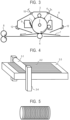
- FIG. 3 illustrates an example of a schematic configuration of an electrophotographic apparatus including a process cartridge 11 including an electrophotographic photosensitive drum 1.
- Reference numeral 1 represents a cylindrical electrophotographic photosensitive drum, and the cylindrical electrophotographic photosensitive drum is rotatably driven about a shaft 2 in the arrow direction at a predetermined peripheral velocity.
- An outer surface of the electrophotographic photosensitive drum 1 is charged with a predetermined positive or negative potential by a charging unit 3.
- a roller charging system using the roller type charging unit 3 is illustrated in FIG. 3 , a charging system such as a corona charging system, a proximity charging system, or an injection charging system may also be adopted.
- the outer surface of the charged electrophotographic photosensitive drum 1 is irradiated with exposure light 4 emitted from an exposing unit (not illustrated), and an electrostatic latent image corresponding to target image information is formed on the outer surface of the electrophotographic photosensitive drum 1.
- the electrostatic latent image formed on the outer surface of the electrophotographic photosensitive drum 1 is developed with a toner stored in a developing unit 5, and a toner image is formed on the outer surface of the electrophotographic photosensitive drum 1.
- the toner image formed on the outer surface of the electrophotographic photosensitive drum 1 is transferred onto a transfer material 7 by a transfer unit 6.
- the transfer material 7 onto which the toner image is transferred is conveyed to a fixing unit 8 to perform a fixing treatment on the toner image.
- the transfer material 7 is printed out the outside of the electrophotographic apparatus.
- the electrophotographic apparatus may also include a cleaning unit 9 for removing an adhered material such as the toner remaining on the outer surface of the electrophotographic photosensitive drum 1 after the transfer.
- the electrophotographic apparatus may also include an antistatic mechanism for an antistatic treatment performed on the outer surface of the electrophotographic photosensitive drum 1 by pre-exposure light 10 from a pre-exposing unit (not illustrated).
- a guiding unit 12 such as a rail may be provided for detachably attaching the process cartridge 11 according to the present invention to the main body of the electrophotographic apparatus.
- the electrophotographic photosensitive drum according to the present invention can be used in, for example, a laser beam printer, an LED printer, a copying machine, a facsimile, and a composite machine thereof.
- an electrophotographic photosensitive drum capable of reducing a frictional force with a cleaning blade and further exhibiting high cleanability even in a case where an abutting pressure of the cleaning blade is low.
- An aluminum cylinder (JIS-A3003, aluminum alloy) having a diameter of 24 mm and a length of 257.5 mm was used as a support (electroconductive support).
- the glass beads were removed from the dispersion with a mesh (opening: 150 ⁇ m). Silicone resin particles (trade name: TOSPEARL 120, average particle size of 2 ⁇ m, manufactured by Momentive Performance Materials, Inc.) as a surface roughness-imparting agent were added to the obtained dispersion. An addition amount of the silicone resin particles was set to 10% by mass with respect to a total mass of the metal oxide particles and the binder material in the dispersion after the glass beads were removed.
- Silicone resin particles trade name: TOSPEARL 120, average particle size of 2 ⁇ m, manufactured by Momentive Performance Materials, Inc.
- silicone oil (trade name: SH28PA, manufactured by Dow Corning Toray Co., Ltd.) as a leveling agent was added to the dispersion so that a content of the silicone oil was 0.01% by mass with respect to the total mass of the metal oxide particles and the binder material in the dispersion.
- a solvent in which methanol and 1-methoxy-2-propanol (mass ratio: 1:1) were mixed with each other was added to the dispersion so that a total mass (that is, a mass of a solid content) of the metal oxide particles, the binder material, and the surface roughness-imparting agent in the dispersion was 67% by mass with respect to a mass of the dispersion.
- a coating liquid for an electroconductive layer was prepared by stirring the mixture.
- the coating liquid for an electroconductive layer was applied onto the support by dip coating, and heating was performed at 140°C for 1 hour, thereby forming an electroconductive layer having a thickness of 30 ⁇ m.
- a coating liquid for a charge transport layer was dissolved in a solvent in which 60 parts of toluene, 2.3 parts of methyl benzoate, and 12.8 parts of tetrahydrofuran were mixed with each other, thereby preparing a coating liquid for a charge transport layer.
- the coating liquid for a charge transport layer was applied onto the charge generation layer by dip coating to form a coating film, and the coating film was dried at 100°C for 20 minutes, thereby forming a charge transport layer having a thickness of 16 ⁇ m.
- the coating liquid for a protection layer was applied onto the charge transport layer by dip coating to form a coating film, and the obtained coating film was dried at 40°C for 5 minutes. Thereafter, the coating film was irradiated with electron beams for 1.6 seconds in a nitrogen atmosphere while rotating a support (an object to be irradiated) at a speed of 300 rpm under conditions of an acceleration voltage of 70 kV and a beam current of 5.0 mA. A dose at a position of the outermost surface layer when irradiating the electron beams was 15 kGy.
- first heating was performed by raising the temperature from 25°C to 100°C for 20 seconds under a nitrogen atmosphere, thereby forming a protection layer having a thickness of 0.3 ⁇ m.
- An oxygen concentration from electron beam irradiation to a subsequent heat treatment was 10 ppm or less.
- the coating film was naturally cooled in the atmospheric air until the temperature of the coating film was 25°C, and then the coating film was subjected to a second heat treatment under a condition in which the temperature of the coating film was 220°C for 15 minutes, thereby forming a wrinkle shape.
- an electrophotographic photosensitive drum according to Example 1 was produced.
- Example 1 each of the type of the charge transporting substance used in the formation of the charge transport layer, the type of the monomer having the polymerizable functional group used in the formation of the protection layer, and the thickness of the protection layer was set as shown in Table 1.
- Each of electrophotographic photosensitive drums according to Examples 2 to 17 was produced in the same manner as that of Example 1 except for this.
- An electrophotographic photosensitive drum produced without performing the second heat treatment in the formation of the protection layer in the Example 1 was prepared.
- An outer surface of the electrophotographic photosensitive drum was polished using a polisher illustrated in FIG. 4 under the following conditions.
- a layer 2-2 obtained by dispersing polishing abrasive grains in a binder resin and provided on a sheet-like substrate 2-3 was used as a polishing sheet.
- An outer surface of an electrophotographic photosensitive drum 2-1 was subjected to a roughening treatment by vertically pressing a surface of the polishing sheet by a vertical mechanism 2-4 for 20 seconds while feeding the polishing sheet parallel to the surface of the polishing sheet and rotating the electrophotographic photosensitive drum 2-1.
- an electrophotographic photosensitive drum according to Comparative Example 1 was produced, the electrophotographic photosensitive drum having an outer surface in which a plurality of parallel groove shapes extending in a circumferential direction of the electrophotographic photosensitive drum were formed.
- the electrophotographic photosensitive drum 2-1 was fixed, and the polishing sheet was fed parallel to an axial direction of the electrophotographic photosensitive drum 2-1 to perform a roughening treatment on the outer surface of the electrophotographic photosensitive drum 2-1.
- the roughening treatment was repeated by changing an angle of a rotation direction of the electrophotographic photosensitive drum 2-1.
- an electrophotographic photosensitive drum according to Comparative Example 2 was produced, the electrophotographic photosensitive drum having an outer surface on which a groove shape was formed in a grid shape.
- a surface shape of a square observation region with one side of 100 ⁇ m on the outer surface of the electrophotographic photosensitive drum was observed under magnification with a laser microscope (VK-X200, manufactured by Keyence Corporation). Subsequently, a first reference line L1 that passes through the central point of the observation region and is parallel to the circumferential direction of the electrophotographic photosensitive drum was provided on an image including concave and convex shapes of wrinkles obtained by the observation. Further, reference lines L2 to L3,600 obtained by rotating the first reference line L1 at every 0.1° around the central point of the observation region were provided.
- Condition 1 was verified for each of the reference lines L1 to L3,600, and a case where all the reference lines L1 to L3,600 satisfied Condition 1 was determined as A, and a case where any one of the reference lines L1 to L3,600 did not satisfy Condition 1 was determined as B.
- Condition 1 The line intersects with the convex portions of the wrinkles at a plurality of locations and has at least two different intersection angles selected from the plurality of intersecting locations.
- the height information of the wrinkles obtained in the surface shape analysis 2 was subjected to frequency analysis to obtain a two-dimensional power spectrum F(r, ⁇ ).
- a distribution function p(r) obtained by making the two-dimensional power spectrum F(r, ⁇ ) one-dimensional in a radial direction was calculated to determine a frequency rp at which p(r) was maximized.
- an angular distribution q( ⁇ ) of F(rp, ⁇ ) was calculated at the frequency rp at which p(r) was maximized, and a case where a variation in power values in the entire ⁇ region was 10% or less was determined as A, and a case where the variation in power values in the entire ⁇ region was greater than 10% was determined as B.
- a modified laser beam printer (trade name: HP LaserJet Enterprise Color M553dn, manufactured by Hewlett-Packard Company) was used.
- an abutting pressure of a cleaning blade against an electrophotographic photosensitive drum was changed to 50% of a product condition.
- the electrophotographic apparatus was modified to measure the amount of drive current of a rotary motor of the electrophotographic photosensitive drum.
- the electrophotographic apparatus was modified to adjust and measure a voltage applied to a charging roller and to adjust and measure the intensity of image exposure light.
- Each of the electrophotographic photosensitive drums according to Examples 1 to 17 and Comparative Example 1 was mounted in a cartridge for a cyan color of the electrophotographic apparatus.
- an electrophotographic photosensitive drum was produced without performing the second heat treatment in the formation of the protection layer in Example 1, and this electrophotographic photosensitive drum is used as a control electrophotographic photosensitive drum for obtaining a control value for obtaining a relative torque value.
- a drive current value (current value B) of the rotary motor of the electrophotographic photosensitive drum obtained by the method described above was measured using the produced control electrophotographic photosensitive drum.
- a ratio of the drive current value (current value A) of the rotary motor of the electrophotographic photosensitive drum obtained as described above to the drive current value (current value B) of the rotary motor of the electrophotographic photosensitive drum obtained as described above was calculated.
- the obtained numerical value of (current value A)/(current value B) was a relative torque value. The smaller the relative torque value, the smaller the frictional force between the electrophotographic photosensitive drum and the cleaning blade.
- Type Type Example 1 (1-1) (1-3) (2-1) (3-1) 0.3
- Example 2 (1-1) (1-3) (2-1) (3-1) 0.5
- Example 3 (1-1) (1-3) (2-1) (3-1) 1.0
- Example 4 (1-1) (1-3) (2-1) (3-1) 1.5
- Example 5 (1-1) (1-3) (2-1) (3-1) 3.0
- Example 6 (1-1) (1-2) (2-1) (3-1) 1.5
- Example 7 (1-1) (1-4) (2-1) (3-1) 1.5
- Example 8 (1-1) (1-5) (2-1) (3-1) 1.5
- Example 9 (1-1) (1-6) (2-1) (3-1) 1.5
- Example 10 (1-1) (1-3) (2-2) (3-1) 1.5
- Example 12 (1-1) (1-3) (2-3) (3-1) 1.5
- Example 13 (1-1) (1-3) (2-4) (3-1) 1.5
- Example 14 (1-1) (1-3) (2-6) (3-1) 1.5
- Example 1 A 0.6 0.220 A 0.64 A
- Example 2 A 1.0 0.113 A 0.63 A
- Example 3 A 2.0 0.056 A 0.61 A
- Example 4 A 2.4 0.040 A 0.60 B
- Example 5 A 6.2 0.015 A 0.58 B
- Example 6 A 3.2 0.030 A 0.59 B
- Example 7 A 3.4 0.031 A 0.59 B
- Example 8 A 3.2 0.035 A 0.60 B
- Example 9 A 3.1 0.033 A 0.61 B
- Example 10 A 2.9 0.029 A 0.60 B
- Example 11 A 3.0 0.030 A 0.59 B
- Example 12 A 3.3 0.030 A 0.60 B
- Example 13 A 3.1 0.031 A 0.58 B
- Example 14 A 3.1 0.033 A 0.59 B
- Example 15 A 3.2 0.034 A 0.62 B
- Example 16 A 2.9 0.031 A 0.60 B
- Example 17 A 3.0 0.030 A 0.60 B Comparative Example 1 B
Landscapes
- Physics & Mathematics (AREA)
- General Physics & Mathematics (AREA)
- Spectroscopy & Molecular Physics (AREA)
- Engineering & Computer Science (AREA)
- Computer Vision & Pattern Recognition (AREA)
- Chemical & Material Sciences (AREA)
- Chemical Kinetics & Catalysis (AREA)
- Photoreceptors In Electrophotography (AREA)
Applications Claiming Priority (1)
| Application Number | Priority Date | Filing Date | Title |
|---|---|---|---|
| JP2020075644A JP7449151B2 (ja) | 2020-04-21 | 2020-04-21 | 電子写真感光ドラム |
Publications (2)
| Publication Number | Publication Date |
|---|---|
| EP3901703A1 EP3901703A1 (en) | 2021-10-27 |
| EP3901703B1 true EP3901703B1 (en) | 2025-06-25 |
Family
ID=75581431
Family Applications (1)
| Application Number | Title | Priority Date | Filing Date |
|---|---|---|---|
| EP21169077.1A Active EP3901703B1 (en) | 2020-04-21 | 2021-04-19 | Electrophotographic photosensitive member |
Country Status (3)
| Country | Link |
|---|---|
| US (1) | US12045006B2 (enExample) |
| EP (1) | EP3901703B1 (enExample) |
| JP (1) | JP7449151B2 (enExample) |
Families Citing this family (8)
| Publication number | Priority date | Publication date | Assignee | Title |
|---|---|---|---|---|
| US11619907B2 (en) * | 2021-03-10 | 2023-04-04 | Canon Kabushiki Kaisha | Process cartridge |
| DE112022003026T5 (de) | 2021-06-11 | 2024-04-04 | Canon Kabushiki Kaisha | Elektrophotographisches lichtempfindliches element, prozesskartusche und elektrophotographisches gerät |
| DE112022003014T5 (de) | 2021-06-11 | 2024-04-25 | Canon Kabushiki Kaisha | Elektrophotographisches lichtempfindliches element, prozesskartusche und elektrophotographisches gerät |
| JP7752992B2 (ja) | 2021-08-06 | 2025-10-14 | キヤノン株式会社 | 電子写真装置 |
| JP7691305B2 (ja) | 2021-08-06 | 2025-06-11 | キヤノン株式会社 | 電子写真感光体、プロセスカートリッジ及び電子写真装置 |
| JP7752991B2 (ja) | 2021-08-06 | 2025-10-14 | キヤノン株式会社 | 電子写真装置 |
| JP2023061679A (ja) | 2021-10-20 | 2023-05-02 | キヤノン株式会社 | 電子写真感光体、プロセスカートリッジ、および電子写真装置 |
| JP2023131675A (ja) | 2022-03-09 | 2023-09-22 | キヤノン株式会社 | 電子写真装置 |
Family Cites Families (83)
| Publication number | Priority date | Publication date | Assignee | Title |
|---|---|---|---|---|
| JPH0727267B2 (ja) | 1986-10-04 | 1995-03-29 | ミノルタ株式会社 | 電子写真の感光体 |
| US4908330A (en) | 1988-02-01 | 1990-03-13 | Canon Kabushiki Kaisha | Process for the formation of a functional deposited film containing group IV atoms or silicon atoms and group IV atoms by microwave plasma chemical vapor deposition process |
| JPH01198481A (ja) | 1988-02-01 | 1989-08-10 | Canon Inc | マイクロ波プラズマcvd法による堆積膜形成法 |
| US5162183A (en) | 1990-07-31 | 1992-11-10 | Xerox Corporation | Overcoat for imaging members |
| JP2992638B2 (ja) | 1995-06-28 | 1999-12-20 | キヤノン株式会社 | 光起電力素子の電極構造及び製造方法並びに太陽電池 |
| JP3879372B2 (ja) * | 2000-07-05 | 2007-02-14 | 富士ゼロックス株式会社 | 有機電子デバイス、電子写真感光体、電子写真画像形成装置およびプロセスカートリッジ |
| CN1306342C (zh) | 2002-04-26 | 2007-03-21 | 佳能株式会社 | 电摄影感光体、成像处理盒和电摄影装置 |
| JP4174391B2 (ja) | 2002-08-30 | 2008-10-29 | キヤノン株式会社 | 電子写真感光体、プロセスカートリッジおよび電子写真装置 |
| US7001699B2 (en) | 2002-08-30 | 2006-02-21 | Canon Kabushiki Kaisha | Electrophotographic photosensitive member, process cartridge and electrophotographic apparatus |
| JP4169726B2 (ja) | 2004-06-25 | 2008-10-22 | 株式会社リコー | 電子写真感光体、画像形成装置、及びプロセスカートリッジ |
| KR101017442B1 (ko) | 2005-12-07 | 2011-02-25 | 캐논 가부시끼가이샤 | 폴리비닐아세탈 수지, 전자 사진 감광체, 공정 카트리지 및전자 사진 장치 |
| JP4380794B2 (ja) | 2007-12-04 | 2009-12-09 | キヤノン株式会社 | 電子写真感光体、電子写真感光体の製造方法、プロセスカートリッジおよび電子写真装置 |
| JP4618311B2 (ja) | 2008-03-19 | 2011-01-26 | 富士ゼロックス株式会社 | 電子写真感光体、プロセスカートリッジ、及び画像形成装置 |
| JP2010066670A (ja) * | 2008-09-12 | 2010-03-25 | Canon Inc | 電子写真感光体の製造方法 |
| JP4696174B2 (ja) | 2009-04-23 | 2011-06-08 | キヤノン株式会社 | 電子写真感光体の製造方法 |
| JP5081271B2 (ja) | 2009-04-23 | 2012-11-28 | キヤノン株式会社 | 電子写真感光体、プロセスカートリッジおよび電子写真装置 |
| JP4743921B1 (ja) | 2009-09-04 | 2011-08-10 | キヤノン株式会社 | 電子写真感光体、プロセスカートリッジおよび電子写真装置 |
| JP5560755B2 (ja) | 2010-02-10 | 2014-07-30 | 富士ゼロックス株式会社 | 電子写真感光体、プロセスカートリッジ、及び画像形成装置 |
| JP5755162B2 (ja) | 2011-03-03 | 2015-07-29 | キヤノン株式会社 | 電子写真感光体の製造方法 |
| JP5079153B1 (ja) | 2011-03-03 | 2012-11-21 | キヤノン株式会社 | 電子写真感光体、プロセスカートリッジおよび電子写真装置、ならびに、電子写真感光体の製造方法 |
| JP5054238B1 (ja) | 2011-03-03 | 2012-10-24 | キヤノン株式会社 | 電子写真感光体の製造方法 |
| JP5827612B2 (ja) | 2011-11-30 | 2015-12-02 | キヤノン株式会社 | ガリウムフタロシアニン結晶の製造方法、及び該ガリウムフタロシアニン結晶の製造方法を用いた電子写真感光体の製造方法 |
| JP5993720B2 (ja) | 2011-11-30 | 2016-09-14 | キヤノン株式会社 | 電子写真感光体、プロセスカートリッジおよび電子写真装置 |
| JP6039368B2 (ja) | 2011-11-30 | 2016-12-07 | キヤノン株式会社 | 電子写真感光体、プロセスカートリッジおよび電子写真装置、ならびに、ガリウムフタロシアニン結晶 |
| JP6071439B2 (ja) | 2011-11-30 | 2017-02-01 | キヤノン株式会社 | フタロシアニン結晶の製造方法、および電子写真感光体の製造方法 |
| JP6105974B2 (ja) | 2012-03-15 | 2017-03-29 | キヤノン株式会社 | 電子写真感光体の製造方法、および電荷輸送層用乳化液 |
| JP6105973B2 (ja) | 2012-03-22 | 2017-03-29 | キヤノン株式会社 | 電子写真感光体の製造方法、電荷輸送層用乳化液 |
| US9029054B2 (en) | 2012-06-29 | 2015-05-12 | Canon Kabushiki Kaisha | Electrophotographic photosensitive member, process cartridge, and electrophotographic apparatus |
| KR101599579B1 (ko) | 2012-06-29 | 2016-03-03 | 캐논 가부시끼가이샤 | 전자 사진 감광체, 프로세스 카트리지 및 전자 사진 장치 |
| JP6108842B2 (ja) | 2012-06-29 | 2017-04-05 | キヤノン株式会社 | 電子写真感光体の製造方法 |
| EP2680075B1 (en) | 2012-06-29 | 2015-12-30 | Canon Kabushiki Kaisha | Electrophotographic photosensitive member, process cartridge, and electrophotographic apparatus |
| JP6049329B2 (ja) | 2012-06-29 | 2016-12-21 | キヤノン株式会社 | 電子写真感光体、電子写真感光体の製造方法、プロセスカートリッジおよび電子写真装置 |
| JP6061761B2 (ja) | 2012-08-30 | 2017-01-18 | キヤノン株式会社 | 電子写真感光体、プロセスカートリッジおよび電子写真装置 |
| JP6218502B2 (ja) | 2012-08-30 | 2017-10-25 | キヤノン株式会社 | 電子写真感光体、プロセスカートリッジおよび電子写真装置 |
| JP2014178425A (ja) | 2013-03-14 | 2014-09-25 | Ricoh Co Ltd | 電子写真感光体、画像形成装置、及びプロセスカートリッジ |
| JP6456126B2 (ja) | 2013-12-26 | 2019-01-23 | キヤノン株式会社 | 電子写真感光体の製造方法 |
| JP6463104B2 (ja) | 2013-12-26 | 2019-01-30 | キヤノン株式会社 | 電子写真感光体、プロセスカートリッジ及び電子写真装置 |
| JP6555877B2 (ja) | 2013-12-26 | 2019-08-07 | キヤノン株式会社 | 電子写真感光体、及び、該電子写真感光体の製造方法、及び該電子写真感光体を有するプロセスカートリッジ及び電子写真装置 |
| JP6423697B2 (ja) | 2013-12-26 | 2018-11-14 | キヤノン株式会社 | 電子写真感光体、電子写真感光体の製造方法、プロセスカートリッジおよび電子写真装置 |
| JP2015143822A (ja) | 2013-12-26 | 2015-08-06 | キヤノン株式会社 | 電子写真感光体、プロセスカートリッジ及び電子写真装置 |
| JP2015143831A (ja) | 2013-12-26 | 2015-08-06 | キヤノン株式会社 | 電子写真感光体、プロセスカートリッジ及び電子写真装置 |
| JP6429636B2 (ja) | 2014-02-24 | 2018-11-28 | キヤノン株式会社 | 電子写真感光体、プロセスカートリッジおよび電子写真装置 |
| JP6444085B2 (ja) | 2014-07-23 | 2018-12-26 | キヤノン株式会社 | 電子写真感光体の製造方法 |
| US9684277B2 (en) | 2014-11-19 | 2017-06-20 | Canon Kabushiki Kaisha | Process cartridge and image-forming method |
| US9599917B2 (en) | 2014-12-26 | 2017-03-21 | Canon Kabushiki Kaisha | Electrophotographic photosensitive member, process cartridge and electrophotographic apparatus |
| JP6508948B2 (ja) | 2015-01-26 | 2019-05-08 | キヤノン株式会社 | 電子写真感光体、電子写真感光体の製造方法、プロセスカートリッジおよび電子写真装置 |
| JP2017010009A (ja) | 2015-06-24 | 2017-01-12 | キヤノン株式会社 | 電子写真感光体、プロセスカートリッジおよび電子写真装置 |
| US20170060008A1 (en) | 2015-08-27 | 2017-03-02 | Canon Kabushiki Kaisha | Image forming method, process cartridge and electrophotographic apparatus |
| JP6639256B2 (ja) | 2016-02-10 | 2020-02-05 | キヤノン株式会社 | 電子写真装置、およびプロセスカートリッジ |
| US10095137B2 (en) | 2016-04-04 | 2018-10-09 | Canon Kabushiki Kaisha | Electrophotographic photosensitive member, method of producing electrophotographic photosensitive member, process cartridge, and electrophotographic image forming apparatus |
| JP6669400B2 (ja) | 2016-04-14 | 2020-03-18 | キヤノン株式会社 | 電子写真感光体、その製造方法、プロセスカートリッジおよび電子写真装置 |
| JP6978858B2 (ja) | 2016-06-21 | 2021-12-08 | キヤノン株式会社 | 電子写真感光体、電子写真感光体の製造方法、該電子写真感光体を有するプロセスカートリッジおよび電子写真装置 |
| US10416581B2 (en) | 2016-08-26 | 2019-09-17 | Canon Kabushiki Kaisha | Electrophotographic photosensitive member, process cartridge, and electrophotographic apparatus |
| JP6884547B2 (ja) * | 2016-10-26 | 2021-06-09 | キヤノン株式会社 | 電子写真感光体の製造方法 |
| JP7060923B2 (ja) | 2017-05-25 | 2022-04-27 | キヤノン株式会社 | 電子写真感光体、プロセスカートリッジおよび電子写真装置 |
| JP6921651B2 (ja) * | 2017-06-29 | 2021-08-18 | キヤノン株式会社 | 電子写真感光体、プロセスカートリッジ及び電子写真装置 |
| JP2019061094A (ja) | 2017-09-27 | 2019-04-18 | 富士ゼロックス株式会社 | 画像形成装置 |
| JP7057104B2 (ja) | 2017-11-24 | 2022-04-19 | キヤノン株式会社 | プロセスカートリッジ及び電子写真画像形成装置 |
| JP7046571B2 (ja) | 2017-11-24 | 2022-04-04 | キヤノン株式会社 | プロセスカートリッジ及び電子写真装置 |
| JP7187270B2 (ja) | 2017-11-24 | 2022-12-12 | キヤノン株式会社 | プロセスカートリッジ及び電子写真装置 |
| JP7034768B2 (ja) | 2018-02-28 | 2022-03-14 | キヤノン株式会社 | プロセスカートリッジ及び画像形成装置 |
| JP7034769B2 (ja) | 2018-02-28 | 2022-03-14 | キヤノン株式会社 | 電子写真感光体、プロセスカートリッジ及び電子写真装置 |
| JP2019152699A (ja) | 2018-02-28 | 2019-09-12 | キヤノン株式会社 | 電子写真感光体、プロセスカートリッジ及び電子写真装置 |
| US10732525B2 (en) * | 2018-04-25 | 2020-08-04 | Canon Kabushiki Kaisha | Electrophotographic apparatus |
| JP7059112B2 (ja) | 2018-05-31 | 2022-04-25 | キヤノン株式会社 | 電子写真感光体、プロセスカートリッジおよび電子写真画像形成装置 |
| JP7129225B2 (ja) | 2018-05-31 | 2022-09-01 | キヤノン株式会社 | 電子写真感光体および電子写真感光体の製造方法 |
| US10747130B2 (en) | 2018-05-31 | 2020-08-18 | Canon Kabushiki Kaisha | Process cartridge and electrophotographic apparatus |
| JP7150485B2 (ja) | 2018-05-31 | 2022-10-11 | キヤノン株式会社 | 電子写真感光体、プロセスカートリッジ及び電子写真装置 |
| JP7059111B2 (ja) | 2018-05-31 | 2022-04-25 | キヤノン株式会社 | 電子写真感光体およびその製造方法、並びにプロセスカートリッジおよび電子写真画像形成装置 |
| JP7054366B2 (ja) | 2018-05-31 | 2022-04-13 | キヤノン株式会社 | 電子写真感光体、プロセスカートリッジおよび電子写真装置 |
| JP2020085991A (ja) | 2018-11-19 | 2020-06-04 | キヤノン株式会社 | 電子写真感光体、プロセスカートリッジ及び電子写真装置 |
| JP2020086308A (ja) | 2018-11-29 | 2020-06-04 | キヤノン株式会社 | 電子写真感光体、電子写真装置、およびプロセスカートリッジ |
| JP7413054B2 (ja) | 2019-02-14 | 2024-01-15 | キヤノン株式会社 | 電子写真感光体、プロセスカートリッジおよび電子写真装置 |
| JP7358276B2 (ja) | 2019-03-15 | 2023-10-10 | キヤノン株式会社 | 電子写真画像形成装置及びプロセスカートリッジ |
| JP7301613B2 (ja) | 2019-06-14 | 2023-07-03 | キヤノン株式会社 | 電子写真感光体、プロセスカートリッジ及び電子写真装置 |
| US11126097B2 (en) | 2019-06-25 | 2021-09-21 | Canon Kabushiki Kaisha | Electrophotographic photosensitive member, process cartridge, and electrophotographic apparatus |
| JP7353824B2 (ja) | 2019-06-25 | 2023-10-02 | キヤノン株式会社 | 電子写真感光体、プロセスカートリッジおよび電子写真装置 |
| JP7269111B2 (ja) | 2019-06-25 | 2023-05-08 | キヤノン株式会社 | 電子写真感光体、プロセスカートリッジおよび電子写真装置 |
| JP7305458B2 (ja) | 2019-06-25 | 2023-07-10 | キヤノン株式会社 | 電子写真感光体、プロセスカートリッジ及び電子写真装置 |
| US11320754B2 (en) | 2019-07-25 | 2022-05-03 | Canon Kabushiki Kaisha | Process cartridge and electrophotographic apparatus |
| US11573499B2 (en) | 2019-07-25 | 2023-02-07 | Canon Kabushiki Kaisha | Process cartridge and electrophotographic apparatus |
| JP7337649B2 (ja) | 2019-10-18 | 2023-09-04 | キヤノン株式会社 | プロセスカートリッジ及び電子写真装置 |
| JP7337652B2 (ja) | 2019-10-18 | 2023-09-04 | キヤノン株式会社 | プロセスカートリッジ及びそれを用いた電子写真装置 |
-
2020
- 2020-04-21 JP JP2020075644A patent/JP7449151B2/ja active Active
-
2021
- 2021-04-14 US US17/230,550 patent/US12045006B2/en active Active
- 2021-04-19 EP EP21169077.1A patent/EP3901703B1/en active Active
Also Published As
| Publication number | Publication date |
|---|---|
| US20210325794A1 (en) | 2021-10-21 |
| EP3901703A1 (en) | 2021-10-27 |
| JP2021173805A (ja) | 2021-11-01 |
| US12045006B2 (en) | 2024-07-23 |
| JP7449151B2 (ja) | 2024-03-13 |
Similar Documents
| Publication | Publication Date | Title |
|---|---|---|
| EP3901703B1 (en) | Electrophotographic photosensitive member | |
| US10838315B2 (en) | Electrophotographic photosensitive member, process cartridge and electrophotographic apparatus | |
| EP3575877B1 (en) | Electrophotographic photosensitive member, process cartridge, and electrophotographic apparatus | |
| EP3575878B1 (en) | Electrophotographic photosensitive member, process cartridge and electrophotographic apparatus | |
| US11256186B2 (en) | Electrophotographic photosensitive member, process cartridge and electrophotographic apparatus | |
| EP3575879B1 (en) | Electrophotographic photosensitive member, process cartridge, and electrophotographic image-forming apparatus | |
| EP3901702B1 (en) | Electrophotographic photosensitive member, process cartridge, and electrophotographic image forming apparatus | |
| US10691033B2 (en) | Electrophotographic photosensitive member, process cartridge, and electrophotographic apparatus | |
| JP2019211545A (ja) | 電子写真感光体および電子写真感光体の製造方法 | |
| US11782353B2 (en) | Method for producing electrophotographic photosensitive member | |
| EP3525042A1 (en) | Electrophotographic photosensitive member, process cartridge, and electrophotographic apparatus | |
| EP4170431A1 (en) | Electrophotographic photosensitive member, process cartridge, and electrophotographic apparatus | |
| EP4057073B1 (en) | Electrophotographic photosensitive member, process cartridge and electrophotographic apparatus | |
| EP4557007A1 (en) | Electrophotographic photosensitive member, process cartridge, and electrophotographic apparatus | |
| EP4557006A1 (en) | Electrophotographic photosensitive member, process cartridge, and electrophotographic apparatus | |
| JP2022140250A (ja) | 電子写真感光体、プロセスカートリッジおよび電子写真装置 | |
| JP2022155779A (ja) | 電子写真感光体、プロセスカートリッジ及び電子写真装置 |
Legal Events
| Date | Code | Title | Description |
|---|---|---|---|
| PUAI | Public reference made under article 153(3) epc to a published international application that has entered the european phase |
Free format text: ORIGINAL CODE: 0009012 |
|
| STAA | Information on the status of an ep patent application or granted ep patent |
Free format text: STATUS: THE APPLICATION HAS BEEN PUBLISHED |
|
| AK | Designated contracting states |
Kind code of ref document: A1 Designated state(s): AL AT BE BG CH CY CZ DE DK EE ES FI FR GB GR HR HU IE IS IT LI LT LU LV MC MK MT NL NO PL PT RO RS SE SI SK SM TR |
|
| B565 | Issuance of search results under rule 164(2) epc |
Effective date: 20210914 |
|
| STAA | Information on the status of an ep patent application or granted ep patent |
Free format text: STATUS: REQUEST FOR EXAMINATION WAS MADE |
|
| 17P | Request for examination filed |
Effective date: 20220428 |
|
| RBV | Designated contracting states (corrected) |
Designated state(s): AL AT BE BG CH CY CZ DE DK EE ES FI FR GB GR HR HU IE IS IT LI LT LU LV MC MK MT NL NO PL PT RO RS SE SI SK SM TR |
|
| GRAP | Despatch of communication of intention to grant a patent |
Free format text: ORIGINAL CODE: EPIDOSNIGR1 |
|
| STAA | Information on the status of an ep patent application or granted ep patent |
Free format text: STATUS: GRANT OF PATENT IS INTENDED |
|
| INTG | Intention to grant announced |
Effective date: 20250327 |
|
| GRAS | Grant fee paid |
Free format text: ORIGINAL CODE: EPIDOSNIGR3 |
|
| GRAA | (expected) grant |
Free format text: ORIGINAL CODE: 0009210 |
|
| STAA | Information on the status of an ep patent application or granted ep patent |
Free format text: STATUS: THE PATENT HAS BEEN GRANTED |
|
| AK | Designated contracting states |
Kind code of ref document: B1 Designated state(s): AL AT BE BG CH CY CZ DE DK EE ES FI FR GB GR HR HU IE IS IT LI LT LU LV MC MK MT NL NO PL PT RO RS SE SI SK SM TR |
|
| REG | Reference to a national code |
Ref country code: GB Ref legal event code: FG4D |
|
| REG | Reference to a national code |
Ref country code: CH Ref legal event code: EP |
|
| REG | Reference to a national code |
Ref country code: CH Ref legal event code: EP |
|
| REG | Reference to a national code |
Ref country code: IE Ref legal event code: FG4D |
|
| REG | Reference to a national code |
Ref country code: DE Ref legal event code: R096 Ref document number: 602021032693 Country of ref document: DE |
|
| PG25 | Lapsed in a contracting state [announced via postgrant information from national office to epo] |
Ref country code: FI Free format text: LAPSE BECAUSE OF FAILURE TO SUBMIT A TRANSLATION OF THE DESCRIPTION OR TO PAY THE FEE WITHIN THE PRESCRIBED TIME-LIMIT Effective date: 20250625 |
|
| REG | Reference to a national code |
Ref country code: LT Ref legal event code: MG9D |
|
| PG25 | Lapsed in a contracting state [announced via postgrant information from national office to epo] |
Ref country code: NO Free format text: LAPSE BECAUSE OF FAILURE TO SUBMIT A TRANSLATION OF THE DESCRIPTION OR TO PAY THE FEE WITHIN THE PRESCRIBED TIME-LIMIT Effective date: 20250925 Ref country code: GR Free format text: LAPSE BECAUSE OF FAILURE TO SUBMIT A TRANSLATION OF THE DESCRIPTION OR TO PAY THE FEE WITHIN THE PRESCRIBED TIME-LIMIT Effective date: 20250926 |
|
| PG25 | Lapsed in a contracting state [announced via postgrant information from national office to epo] |
Ref country code: BG Free format text: LAPSE BECAUSE OF FAILURE TO SUBMIT A TRANSLATION OF THE DESCRIPTION OR TO PAY THE FEE WITHIN THE PRESCRIBED TIME-LIMIT Effective date: 20250625 |
|
| PG25 | Lapsed in a contracting state [announced via postgrant information from national office to epo] |
Ref country code: HR Free format text: LAPSE BECAUSE OF FAILURE TO SUBMIT A TRANSLATION OF THE DESCRIPTION OR TO PAY THE FEE WITHIN THE PRESCRIBED TIME-LIMIT Effective date: 20250625 |
|
| PG25 | Lapsed in a contracting state [announced via postgrant information from national office to epo] |
Ref country code: RS Free format text: LAPSE BECAUSE OF FAILURE TO SUBMIT A TRANSLATION OF THE DESCRIPTION OR TO PAY THE FEE WITHIN THE PRESCRIBED TIME-LIMIT Effective date: 20250925 |
|
| PG25 | Lapsed in a contracting state [announced via postgrant information from national office to epo] |
Ref country code: LV Free format text: LAPSE BECAUSE OF FAILURE TO SUBMIT A TRANSLATION OF THE DESCRIPTION OR TO PAY THE FEE WITHIN THE PRESCRIBED TIME-LIMIT Effective date: 20250625 |
|
| REG | Reference to a national code |
Ref country code: NL Ref legal event code: MP Effective date: 20250625 |
|
| PG25 | Lapsed in a contracting state [announced via postgrant information from national office to epo] |
Ref country code: NL Free format text: LAPSE BECAUSE OF FAILURE TO SUBMIT A TRANSLATION OF THE DESCRIPTION OR TO PAY THE FEE WITHIN THE PRESCRIBED TIME-LIMIT Effective date: 20250625 |
|
| PG25 | Lapsed in a contracting state [announced via postgrant information from national office to epo] |
Ref country code: PT Free format text: LAPSE BECAUSE OF FAILURE TO SUBMIT A TRANSLATION OF THE DESCRIPTION OR TO PAY THE FEE WITHIN THE PRESCRIBED TIME-LIMIT Effective date: 20251027 |
|
| REG | Reference to a national code |
Ref country code: AT Ref legal event code: MK05 Ref document number: 1807083 Country of ref document: AT Kind code of ref document: T Effective date: 20250625 |