EP2856639B1 - Low noise amplifiers for carrier aggregation - Google Patents
Low noise amplifiers for carrier aggregation Download PDFInfo
- Publication number
- EP2856639B1 EP2856639B1 EP13728878.3A EP13728878A EP2856639B1 EP 2856639 B1 EP2856639 B1 EP 2856639B1 EP 13728878 A EP13728878 A EP 13728878A EP 2856639 B1 EP2856639 B1 EP 2856639B1
- Authority
- EP
- European Patent Office
- Prior art keywords
- signal
- input
- amplifier stage
- output
- circuit
- Prior art date
- Legal status (The legal status is an assumption and is not a legal conclusion. Google has not performed a legal analysis and makes no representation as to the accuracy of the status listed.)
- Active
Links
Images


Classifications
-
- H—ELECTRICITY
- H03—ELECTRONIC CIRCUITRY
- H03F—AMPLIFIERS
- H03F3/00—Amplifiers with only discharge tubes or only semiconductor devices as amplifying elements
- H03F3/20—Power amplifiers, e.g. Class B amplifiers, Class C amplifiers
- H03F3/21—Power amplifiers, e.g. Class B amplifiers, Class C amplifiers with semiconductor devices only
- H03F3/211—Power amplifiers, e.g. Class B amplifiers, Class C amplifiers with semiconductor devices only using a combination of several amplifiers
-
- H—ELECTRICITY
- H03—ELECTRONIC CIRCUITRY
- H03F—AMPLIFIERS
- H03F1/00—Details of amplifiers with only discharge tubes, only semiconductor devices or only unspecified devices as amplifying elements
- H03F1/08—Modifications of amplifiers to reduce detrimental influences of internal impedances of amplifying elements
- H03F1/22—Modifications of amplifiers to reduce detrimental influences of internal impedances of amplifying elements by use of cascode coupling, i.e. earthed cathode or emitter stage followed by earthed grid or base stage respectively
- H03F1/223—Modifications of amplifiers to reduce detrimental influences of internal impedances of amplifying elements by use of cascode coupling, i.e. earthed cathode or emitter stage followed by earthed grid or base stage respectively with MOSFET's
-
- H—ELECTRICITY
- H03—ELECTRONIC CIRCUITRY
- H03F—AMPLIFIERS
- H03F3/00—Amplifiers with only discharge tubes or only semiconductor devices as amplifying elements
- H03F3/189—High frequency amplifiers, e.g. radio frequency amplifiers
- H03F3/19—High frequency amplifiers, e.g. radio frequency amplifiers with semiconductor devices only
- H03F3/193—High frequency amplifiers, e.g. radio frequency amplifiers with semiconductor devices only with field-effect devices
-
- H—ELECTRICITY
- H03—ELECTRONIC CIRCUITRY
- H03F—AMPLIFIERS
- H03F3/00—Amplifiers with only discharge tubes or only semiconductor devices as amplifying elements
- H03F3/68—Combinations of amplifiers, e.g. multi-channel amplifiers for stereophonics
-
- H—ELECTRICITY
- H03—ELECTRONIC CIRCUITRY
- H03F—AMPLIFIERS
- H03F3/00—Amplifiers with only discharge tubes or only semiconductor devices as amplifying elements
- H03F3/72—Gated amplifiers, i.e. amplifiers which are rendered operative or inoperative by means of a control signal
-
- H—ELECTRICITY
- H03—ELECTRONIC CIRCUITRY
- H03G—CONTROL OF AMPLIFICATION
- H03G3/00—Gain control in amplifiers or frequency changers without distortion of the input signal
- H03G3/20—Automatic control
-
- H—ELECTRICITY
- H04—ELECTRIC COMMUNICATION TECHNIQUE
- H04L—TRANSMISSION OF DIGITAL INFORMATION, e.g. TELEGRAPHIC COMMUNICATION
- H04L27/00—Modulated-carrier systems
- H04L27/26—Systems using multi-frequency codes
- H04L27/2601—Multicarrier modulation systems
- H04L27/2647—Arrangements specific to the receiver only
-
- H—ELECTRICITY
- H03—ELECTRONIC CIRCUITRY
- H03F—AMPLIFIERS
- H03F2200/00—Indexing scheme relating to amplifiers
- H03F2200/451—Indexing scheme relating to amplifiers the amplifier being a radio frequency amplifier
Definitions
- the present disclosure relates generally to electronics, and more specifically to low noise amplifiers (LNAs).
- LNAs low noise amplifiers
- a wireless device in a wireless communication system may transmit and receive data for two-way communication.
- the wireless device may include a transmitter for data transmission and a receiver for data reception.
- the transmitter may modulate a radio frequency (RF) carrier signal with data to obtain a modulated RF signal, amplify the modulated RF signal to obtain an amplified RF signal having the proper output power level, and transmit the amplified RF signal via an antenna to a base station.
- the receiver may obtain a received RF signal via the antenna and may amplify and process the received RF signal to recover data sent by the base station.
- RF radio frequency
- a wireless device may support carrier aggregation, which is simultaneous operation on multiple carriers.
- a carrier may refer to a range of frequencies used for communication and may be associated with certain characteristics. For example, a carrier may be associated with system information describing operation on the carrier.
- a carrier may also be referred to as a component carrier (CC), a frequency channel, a cell, etc. It is desirable to efficiently support carrier aggregation by the wireless device.
- Prior art RF receiver front-ends are known from US2012/056681 , US2011/217945 , US2005/265084 , and US2008/116976 .
- LNAs supporting carrier aggregation are disclosed herein. These LNAs may have better performance and may be used for various types of electronic devices such as wireless communication devices.
- FIG. 1 shows a wireless device 110 communicating with a wireless communication system 120.
- Wireless system 120 may be a Long Term Evolution (LTE) system, a Code Division Multiple Access (CDMA) system, a Global System for Mobile Communications (GSM) system, a wireless local area network (WLAN) system, or some other wireless system.
- LTE Long Term Evolution
- CDMA Code Division Multiple Access
- GSM Global System for Mobile Communications
- WLAN wireless local area network
- a CDMA system may implement Wideband CDMA (WCDMA), cdma2000, or some other version of CDMA.
- FIG. 1 shows wireless system 120 including two base stations 130 and 132 and one system controller 140.
- a wireless system may include any number of base stations and any set of network entities.
- Wireless device 110 may also be referred to as a user equipment (UE), a mobile station, a terminal, an access terminal, a subscriber unit, a station, etc.
- Wireless device 110 may be a cellular phone, a smartphone, a tablet, a wireless modem, a personal digital assistant (PDA), a handheld device, a laptop computer, a smartbook, a netbook, a cordless phone, a wireless local loop (WLL) station, a Bluetooth device, etc.
- Wireless device 110 may be capable of communicating with wireless system 120.
- Wireless device 110 may also be capable of receiving signals from broadcast stations (e.g., a broadcast station 134), signals from satellites (e.g., a satellite 150) in one or more global navigation satellite systems (GNSS), etc.
- Wireless device 110 may support one or more radio technologies for wireless communication such as LTE, cdma2000, WCDMA, GSM, 802.11, etc.
- Wireless device 110 may support carrier aggregation, which is operation on multiple carriers. Carrier aggregation may also be referred to as multi-carrier operation. Wireless device 110 may be able to operate in low-band from 698 to 960 megahertz (MHz), mid-band from 1475 to 2170 MHz, and/or high-band from 2300 to 2690 and 3400 to 3800 MHz. Low-band, mid-band, and high-band refer to three groups of bands (or band groups), with each band group including a number of frequency bands (or simply, "bands"). Each band may cover up to 200 MHz and may include one or more carriers. Each carrier may cover up to 20 MHz in LTE. LTE Release 11 supports 35 bands, which are referred to as LTE/UMTS bands and are listed in 3GPP TS 36.101. Wireless device 110 may be configured with up to 5 carriers in one or two bands in LTE Release 11.
- carrier aggregation may be categorized into two types - intra-band CA and inter-band CA.
- Intra-band CA refers to operation on multiple carriers within the same band.
- Inter-band CA refers to operation on multiple carriers in different bands.
- FIG. 2A shows an example of contiguous intra-band CA.
- wireless device 110 is configured with four contiguous carriers in the same band, which is a band in low-band. Wireless device 110 may receive transmissions on multiple contiguous carriers within the same band.
- FIG. 2B shows an example of non-contiguous intra-band CA.
- wireless device 110 is configured with four non-contiguous carriers in the same band, which is a band in low-band.
- the carriers may be separated by 5 MHz, 10 MHz, or some other amount.
- Wireless device 110 may receive transmissions on multiple non-contiguous carriers within the same band.
- FIG. 2C shows an example of inter-band CA in the same band group.
- wireless device 110 is configured with four carriers in two bands in the same band group, which is low-band.
- Wireless device 110 may receive transmissions on multiple carriers in different bands in the same band group (e.g., low-band in FIG. 2C ).
- FIG. 2D shows an example of inter-band CA in different band groups.
- wireless device 110 is configured with four carriers in two bands in different band groups, which include two carriers in one band in low-band and two additional carriers in another band in mid-band.
- Wireless device 110 may receive transmissions on multiple carriers in different bands in different band groups (e.g., low-band and mid-band in FIG. 2D ).
- FIGS. 2A to 2D show four examples of carrier aggregation.
- Carrier aggregation may also be supported for other combinations of bands and band groups.
- carrier aggregation may be supported for low-band and high-band, mid-band and high-band, high-band and high-band, etc.
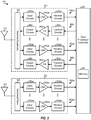
- FIG. 3 shows a block diagram of an exemplary design of wireless device 110 in FIG. 1 .
- wireless device 110 includes a transceiver 320 coupled to a primary antenna 310, receivers 322 coupled to a secondary antenna 312, and a data processor/controller 380.
- Transceiver 320 includes multiple (K) receivers 330aa to 330ak and multiple (K) transmitters 360a to 360k to support multiple bands, carrier aggregation, multiple radio technologies, etc.
- Receivers 322 include multiple (M) receivers 330ba to 330bm to support multiple bands, carrier aggregation, multiple radio technologies, receive diversity, MIMO transmission, etc.
- each receiver 330 includes input circuits 332, an LNA 340, and receive circuits 342.
- antenna 310 receives signals from base stations and/or other transmitter stations and provides a received RF signal, which is routed through switches/duplexers 324 and provided to a selected receiver.
- receiver 330aa is the selected receiver.
- the received RF signal is passed through input circuits 332aa, which provides an input RF signal to an LNA 340aa.
- Input circuits 332aa may include a matching circuit, a receive filter, etc.
- LNA 340aa amplifies the input RF signal and provides an output RF signal.
- Receive circuits 342aa amplify, filter, and downconvert the output RF signal from RF to baseband and provide an analog input signal to data processor 380.
- Receive circuits 332aa may include mixers, a filter, an amplifier, a matching circuit, an oscillator, a local oscillator (LO) generator, a phase locked loop (PLL), etc.
- Each remaining receiver 330 in transceiver 320 and each receiver 330 in receivers 322 may operate in similar manner as receiver 330aa in transceiver 320.
- each transmitter 360 includes transmit circuits 362, a power amplifier (PA) 364, and output circuits 366.
- data processor 380 processes (e.g., encodes and modulates) data to be transmitted and provides an analog output signal to a selected transmitter.
- transmitter 360a is the selected transmitter.
- transmit circuits 362a amplify, filter, and upconvert the analog output signal from baseband to RF and provide a modulated RF signal.
- Transmit circuits 362a may include mixers, an amplifier, a filter, a matching circuit, an oscillator, an LO generator, a PLL, etc.
- a PA 364a receives and amplifies the modulated RF signal and provides an amplified RF signal having the proper output power level.
- the amplified RF signal is passed through output circuits 366a, routed through switches/duplexers 324, and transmitted via antenna 310.
- Output circuits 366a may include a matching circuit, a transmit filter, a directional coupler, etc.
- FIG. 3 shows an exemplary design of receivers 330 and transmitters 360.
- a receiver and a transmitter may also include other circuits not shown in FIG. 3 , such as filters, matching circuits, etc.
- All or a portion of transceiver 320 and receivers 322 may be implemented on one or more analog integrated circuits (ICs), RF ICs (RFICs), mixed-signal ICs, etc.
- ICs analog integrated circuits
- RFICs RF ICs
- mixed-signal ICs etc.
- LNAs 340, receive circuits 342, and transmit circuits 362 may be implemented on one module, which may be an RFIC, etc.
- Switches/duplexers 324, switches/filters 326, input circuits 332, output circuits 366, and PAs 364 may be implemented on another module, which may be a hybrid module, etc.
- the circuits in receivers 330 and transmitters 360 may also be implemented in other manners.
- Data processor/controller 380 may perform various functions for wireless device 110. For example, data processor 380 may perform processing for data being received via receivers 330 and data being transmitted via transmitters 360. Controller 380 may control the operation of switches/duplexers 324, switches/filters 326, input circuits 332, LNAs 340, receive circuits 342, transmit circuits 362, PAs 364, output circuits 366, or a combination thereof.
- a memory 382 may store program codes and data for data processor/controller 380.
- Data processor/controller 380 may be implemented on one or more application specific integrated circuits (ASICs) and/or other ICs.
- ASICs application specific integrated circuits
- Wireless device 110 may receive multiple transmissions from one or more cells/base stations on multiple carriers at different frequencies for carrier aggregation. For intra-band CA, the multiple transmissions are sent on multiple carriers in the same band. For inter-band CA, the multiple transmissions are sent on multiple carriers in different bands.
- FIG. 4A shows a block diagram of an exemplary design of a receiver 400 that includes a CA LNA 440 supporting no CA and intra-band CA.
- CA LNA 440 may be used for one or more LNAs 340 within wireless device 110 in FIG. 3 .
- an antenna 410 receives transmissions on multiple carriers in the same band and provides a received RF signal.
- the received RF signal is routed through switches/duplexers 424 and provided as a receiver input signal, RXin, to an input matching circuit 432.
- Matching circuit 432 performs power and/or impedance matching between CA LNA 440 and either switches/duplexers 424 or antenna 410 for one or more bands of interest.
- Matching circuit 432 which may be part of one of input circuits 332 in FIG. 3 , provides an input RF signal, RFin, to CA LNA 440.
- CA LNA 440 receives the input RF signal from matching circuit 432, amplifies the input RF signal, and provides up to M output RF signals, RFout1 to RFoutM, via up to M LNA outputs, where M > 1.
- M load circuits 490a to 490m are coupled to the M LNA outputs.
- Each load circuit 490 may include one or more inductors, capacitors, transistors, mixers, etc.
- Each load circuit 490 may be part of one of receive circuits 342 in FIG. 3 .
- Each output RF signal may be provided to one or more mixers within one load circuit 490 and may be downconverted by the associated mixer(s) such that transmissions on one or more carriers of interest are downconverted from RF to baseband.
- a CA LNA such as CA LNA 440 in FIG. 4A , may operate in a non-CA mode or a CA mode at any given moment.
- the CA LNA operates in a 1-input 1-output (1 ⁇ 1) configuration, receives one input RF signal comprising one or more transmissions on one set of carriers, and provides one output RF signal to one load circuit.
- the CA LNA operates in a 1 ⁇ M configuration, receives one input RF signal comprising multiple transmissions on M sets of carriers, and provides M output RF signals to M load circuits, one output RF signal for each set of carriers, where M > 1.
- Each set of carriers may include one or more carriers in one band.
- FIG. 4B shows a schematic diagram of an exemplary design of a CA LNA 440x supporting no CA and intra-band CA on two sets of carriers in the same band.
- CA LNA 440x is one exemplary design of CA LNA 440 in FIG. 4A .
- CA LNA 440x receives an input RF signal from input matching circuit 432 and provides up to two output RF signals, RFout1 and RFout2, for up to two sets of carriers.
- the first output RF signal is provided to a load circuit 490x, and the second output RF signal is provided to a load circuit 490y.
- load circuit 490x includes two mixers 492a and 492b coupled to two baseband filters 494a and 494b, respectively.
- Mixers 492a and 492b implement a quadrature downconverter for a first set of carriers.
- Mixer 492a receives the first output RF signal from CA LNA 440x and an inphase LO signal, ILO1, at a first mixing frequency for the first set of carriers.
- Mixer 492a downconverts the first output RF signal with the ILO1 signal and provides an inphase (I) downconverted signal.
- Mixer 492b receives the first output RF signal from CA LNA 440x and a quadrature LO signal, QLO1, at the first mixing frequency for the first set of carriers.
- Mixer 492b downconverts the first output RF signal with the QLO1 signal and provides a quadrature (Q) downconverted signal.
- Filters 494a and 494b receive and filter the I and Q downconverted signals from mixers 492a and 492b, respectively, and provide I and Q baseband signals, Vout1, for the first set of carriers.
- Mixers 492c and 492d and filters 494c and 494d within load circuit 490y similarly process the second output RF signal from CA LNA 440x and provide I and Q baseband signals for a second set of carriers.
- Mixers 492c and 492d receive the second RF signal and I and Q LO signals, respectively, at a second mixing frequency for the second set of carriers.
- Mixers 492c and 492d downconvert the second output RF signal with the I and Q LO signals and provide the I and Q downconverted signals, respectively.
- Filters 494c and 494d receive and filter the I and Q downconverted signals from mixers 492c and 492d, respectively, and provide I and Q baseband signals, Vout2, for the second set of carriers.
- FIG. 4B shows an exemplary design of load circuits 490x and 490y.
- a load circuit may also comprise different and/or additional circuits.
- a load circuit may include an amplifier coupled before the mixers, or between the mixers and the filters, or after the filters.
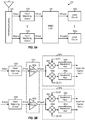
- FIG. 5A shows a block diagram of an exemplary design of a receiver 500 that includes a MIMO LNA 540 supporting no CA, intra-band CA, and inter-band CA.
- MIMO LNA 540 may be used for one or more LNAs 340 within wireless device 110 in FIG. 3 .
- an antenna 510 receives transmissions on one or more carriers in the same band or different bands and provides a received RF signal to switches/ duplexers 524.
- Switches/duplexers 524 provide up to N receiver input signals, RXin1 to RXinN, to up to N input matching circuits 532a to 532n, respectively, where N > 1.
- Matching circuits 532a to 532n may be part of one or more input circuits 332 in FIG. 3 .
- Each matching circuit 532 performs power and/or impedance matching between MIMO LNA 540 and either switches/duplexers 524 or antenna 510 for one or more bands of interest.
- the N matching circuits 532a to 532n may be designed for different bands and may provide up to N input RF signals, RFin1 to RFinN.
- MIMO LNA 540 receives up to N input RF signals and amplifies (i) one input RF signal for no CA or intra-band CA or (ii) multiple input RF signals for inter-band CA.
- MIMO LNA 540 provides up to M output RF signals, RFout1 to RFoutM, via up to M LNA outputs.
- M load circuits 590a to 590m are coupled to the M LNA outputs.
- Each load circuit 590 may include one or more inductors, capacitors, transistors, mixers, etc.
- Each output RF signal may be provided to one or more mixers within one load circuit 590 and may be downconverted by the associated mixer(s) such that one or more transmissions on one or more carriers of interest are downconverted from RF to baseband.
- a MIMO LNA such as MIMO LNA 540 in FIG. 5A , may operate in a non-CA mode, an intra-band CA mode, or an inter-band CA mode at any given moment.
- the MIMO LNA operates in a 1 ⁇ 1 configuration, receives one input RF signal comprising one or more transmissions on one set of carriers, and provides one output RF signal to one load circuit.
- the MIMO LNA operates in a 1 ⁇ M configuration, receives one input RF signal comprising multiple transmissions on M sets of carriers in the same band, and provides M output RF signals to M load circuits, one output RF signal for each set of carriers, where M > 1.
- the MIMO LNA operates in an N ⁇ M configuration, receives N input RF signals comprising multiple transmissions on M sets of carriers in up to N different bands, and provides M output RF signals to M load circuits, where M > 1 and N > 1.
- the N input RF signals may correspond to up to N different bands.
- a MIMO LNA such as MIMO LNA 540 in FIG. 5A , may be used to receive transmissions on multiple carriers at different frequencies.
- a MIMO LNA may include multiple outputs providing multiple output RF signals for different carriers or different sets of carriers of interest.
- a MIMO LNA is different from LNAs used to receive a MIMO transmission sent from multiple transmit antennas to multiple receive antennas.
- An LNA for a MIMO transmission typically has (i) one input receiving one input RF signal from one receive antenna and (ii) one output providing one output RF signal.
- the multiple outputs of a MIMO LNA thus cover frequency dimension whereas the outputs of LNAs used for a MIMO transmission cover spatial dimension.
- FIG. 5B shows a schematic diagram of an exemplary design of a MIMO LNA 540x supporting no CA, intra-band CA, and inter-band CA on two sets of carriers in different bands.
- Each set of carriers may include one or more carriers in one band.
- MIMO LNA 540x is one exemplary design of MIMO LNA 540 in FIG. 5A .
- Matching circuits 532a and 532b may receive (i) the same receiver input signal from one antenna or (ii) different receiver input signals from one or more antennas. Hence, the RXin2 signal may or may not be equal to the RXin1 signal in FIG. 5B .
- Each matching circuit 532 performs power and/or impedance matching for one or more bands of interest.
- MIMO LNA 540x includes two amplifier stages 550a and 550b for two sets of carriers.
- Amplifier stage 550a receives and amplifies the first input RF signal from matching circuit 532a and provides a first output RF signal, RFout1, for a first set of carriers.
- Amplifier stage 550b receives and amplifies the second input RF signal from matching circuit 532b and provides a second output RF signal, RFout2, for a second set of carriers.
- MIMO LNA 540x may include circuitry to route an output RF signal from each amplifier stage 550 to any one of load circuits 590x and 590y.
- load circuit 590x includes two mixers 592a and 592b coupled to two baseband filters 594a and 594b, respectively.
- Mixer 592a receives the first output RF signal from amplifier stage 550a and an inphase LO signal, ILO1, at a first mixing frequency for the first set of carriers.
- Mixer 592a downconverts the first output RF signal with the ILO1 signal and provides an I downconverted signal.
- Mixer 592b receives the first output RF signal from amplifier stage 550b and a quadrature LO signal, QLO1, at the first mixing frequency for the first set of carriers.
- Mixer 592b downconverts the first output RF signal with the QLO1 signal and provides a Q downconverted signal.
- Filters 594a and 594b receive and filter the I and Q downconverted signals from mixers 592a and 592b, respectively, and provide I and Q baseband signals, Vout1, for the first set of carriers.
- Mixers 592c and 592d and filters 594c and 594d within load circuit 590y similarly process the second output RF signal from amplifier stage 550b and provide I and Q baseband signals, Vout2, for a second set of carriers.
- CA LNA 440 in FIG. 4A may be implemented in various manners. Some exemplary designs of CA LNA 440 are described below. CA LNA 440 may also be implemented with transistors of various types. Some exemplary designs of CA LNA 440 using N-channel metal oxide semiconductor (NMOS) transistors are described below.
- NMOS N-channel metal oxide semiconductor
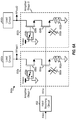
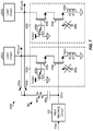
- FIG. 6A shows a schematic diagram of an exemplary design of a CA LNA 640a with inductive degeneration and cascode shutoff.
- CA LNA 640a is one exemplary design of CA LNA 440 in FIG. 4A .
- CA LNA 640a includes two amplifier stages 650a and 650b coupled to a common input matching circuit 632 and to two load circuits 690a and 690b.
- Matching circuit 632 receives a receiver input signal, RXin, performs input matching for CA LNA 640a, and provides an input RF signal, RFin.
- Matching circuit 632 may correspond to matching circuit 432 in FIG. 4A .
- Load circuits 690a and 690b may correspond to load circuits 490a and 490m in FIG. 4A .
- CA LNA 640a receives the input RF signal, which may include transmissions on two sets of carriers, with each set including one or more carriers.
- amplifier stage 650a includes a source degeneration inductor 652a, a gain transistor 654a, and a cascode transistor 656a.
- Gain transistor 654a and cascode transistor 656a may be implemented with NMOS transistors (as shown in FIG. 6A ) or with transistors of other types.
- Gain transistor 654a has its gate coupled to matching circuit 632 and its source coupled to one end of inductor 652a. The other end of inductor 652a is coupled to circuit ground.
- Cascode transistor 656a has its source coupled to the drain of gain transistor 654a and its drain coupled to load circuit 690a.
- a switch 658a has its input port coupled to the gate of cascode transistor 656a, its first output port coupled to a bias voltage, Vcasc, and its second output port coupled to circuit ground.
- Amplifier stage 650b includes a source degeneration inductor 652b, a gain transistor 654b, a cascode transistor 656b, and a switch 658b, which are coupled in similar manner as inductor 652a, gain transistor 654a, cascode transistor 656a, and switch 658a in amplifier stage 650a.
- FIG. 6A shows CA LNA 640a including two amplifier stages 650a and 650b for two sets of carriers.
- Amplifier stages 650a and 650b may be independently enabled or disabled via switches 658a and 658b, respectively.
- CA LNA 640a may include more than two amplifier stages 650 for more than two sets of carriers.
- An input RF signal may include transmissions on multiple sets of carriers in the same band and may be referred to as a carrier-aggregated RF signal.
- the carrier-aggregated RF signal may be downconverted using LO signals at different frequencies corresponding to the center frequencies of the multiple sets of carriers on which the transmissions are sent.
- the carrier-aggregated RF signal may be split at the LNA input in order to achieve good LO-LO isolation between the LO signals for the multiple sets of carriers.
- CA LNA 640a includes two amplifier stages 650a and 650b to amplify the carrier-aggregated RF signal and provide two output RF signals to two separate downconverters in the two load circuits 690a and 690b.
- CA LNA 640a may operate in a non-CA mode or a CA mode at any given moment.
- CA LNA 640a receives transmissions on one set of carriers and provides one output RF signal to one load circuit.
- CA mode CA LNA 640a receives transmissions on two sets of carriers and provides two output RF signals to two load circuits, one output RF signal for each set of carriers.
- FIG. 6B shows operation of CA LNA 640a in the CA mode.
- both amplifier stages 650a and 650b are enabled by connecting the gate of cascode transistor 656a to the Vcasc voltage via switch 658a and coupling the gate of cascode transistor 656b to the Vcasc voltage via switch 658b.
- Amplifier stage 650a amplifies the input RF signal and provides the first output RF signal to load circuit 690a.
- Amplifier stage 650b amplifies the input RF signal and provides the second output RF signal to load circuit 690b.
- FIG. 6C shows operation of CA LNA 640a in the non-CA mode.
- the non-CA mode only one amplifier stage is enabled, and the other amplifier stage is disabled.
- amplifier stage 650a is enabled by connecting the gate of cascode transistor 656a to the Vcasc voltage via switch 658a, and amplifier stage 650b is disabled by shorting the gate of cascode transistor 656b to circuit ground via switch 658b.
- Amplifier stage 650a amplifies the input RF signal and provides an output RF signal to load circuit 690a.
- amplifier stage 650b is enabled, and amplifier stage 650a is disabled (not shown in FIG. 6C ). In this configuration, amplifier stage 650b amplifies the input RF signal and provides an output RF signal to load circuit 690b.
- source degeneration inductors 652a and 652b are used for amplifier stages 650a and 650b in order to reduce interaction between the two amplifier stages and to help reduce noise figure (NF) degradation.
- Source degeneration inductors 652a and 652b may also improve linearity of amplifier stages 650a and 650b and help input impedance matching of CA LNA 640a.
- Inductors 652a and 652b may have the same value or different values.
- the values of inductors 652a and 652b may be selected (e.g., independently) based on a trade-off between voltage gain and linearity in the CA mode and the non-CA mode.
- a variable capacitor 668a may be present across the gate and source of gain transistor 654a.
- Capacitor 668a may include parasitic of gain transistor 654a.
- Capacitor 668a may also include a bank of switchable capacitors, which may be coupled between the gain and source of gain transistor 654a and may be used to fine-tune the input impedance of CA LNA 640a. Each switchable capacitor may be implemented with a capacitor coupled in series with a switch.
- a variable capacitor 668b may be present across the gate and source of gain transistor 654b.
- Capacitor 668b may include a bank of switchable capacitors, which may be coupled between the gain and source of gain transistor 654b and may be used to fine-tune the input impedance.
- Input matching circuit 632 is common to both amplifier stages 650a and 650b and is used in both the CA mode and the non-CA mode.
- CA mode both amplifier stages 650a and 650b are enabled, and gain transistors 654a and 654b operate in a saturation region, as shown in FIG. 6B .
- non-CA mode one amplifier stage (e.g., amplifier stage 650a) is enabled, and the other amplifier stage (e.g., amplifier stage 650b) is disabled. However, the gain transistor in the disabled amplifier stage (e.g., gain transistor 654b in amplifier stage 650b) is turned On by the input RF signal that is applied to both gain transistors 654a and 654b.
- the gain transistor in the disabled amplifier stage operates in a linear region.
- a gain transistor may operate in the saturation region when an amplifier stage is enabled and may operate in the linear region when the amplifier stage is disabled. Operating the gain transistor of the disabled amplifier stage in the linear region may help to reduce changes in the input impedance of CA LNA 640a between the CA mode and the non-CA mode, without a current penalty in the disabled amplifier stage.
- CA LNA 640a splits the carrier-aggregated RF signal at the "gate” level by having the carrier-aggregated RF signal applied to two gain transistors 654a and 654b.
- the carrier-aggregated RF signal may also be split at the "cascode” level by having the carrier-aggregated RF signal applied to a single gain transistor driving two cascode transistors.
- Splitting the carrier-aggregated RF signal at the gate level may provide better performance (e.g., better gain, noise figure, linearity, and isolation) than splitting the carrier-aggregated RF signal at the cascode level. For example, splitting the carrier-aggregated RF signal at the gate level may provide good LO-LO isolation of about 35 dB whereas splitting the carrier-aggregated RF signal at the cascode level may provide LO-LO isolation of only about 15 dB.
- FIG. 7 shows a schematic diagram of an exemplary design of a CA LNA 640b with inductive degeneration, cascode shutoff, and resistive feedback.
- CA LNA 640b is another exemplary design of CA LNA 440 in FIG. 4A .
- CA LNA 640b includes two amplifier stages 650a and 650b coupled to a common input matching circuit 632 and to two load circuits 690a and 690b, similar to CA LNA 640a in FIG. 6A .
- CA LNA 640b further includes a feedback circuit 660 coupled between the drains of cascode transistors 656a and 656b and the gates of gain transistors 654a and 654b, i.e., between the input and output of amplifier stages 650a and 650b.
- feedback circuit 660 includes switches 662a and 662b, a resistor 664, and a capacitor 666. Resistor 664 and capacitor 666 are coupled in series, with the bottom terminal of capacitor 666 being coupled to the gates of gain transistors 654a and 654b.
- Switch 662a is coupled between the drain of cascode transistor 656a and the top terminal of resistor 664.
- Switch 662b is coupled between the drain of cascode transistor 656b and the top terminal of resistor 664. Switches 662a and 662b may each be closed to connect feedback circuit 660 to its associated cascode transistor 656 and may be opened to disconnect feedback circuit 660 from the associated cascode transistor 656.
- a feedback path from RFout1 to feedback circuit 660 may be formed by closing switch 662a.
- a feedback path from RFout2 to feedback circuit 660 may be formed by closing switch 662b.
- Feedback circuit 660 may also include one or more active circuits such as a transistor.
- feedback circuit 660 may be used/enabled for low-band to provide input power match. For mid-band and high-band, feedback circuit 660 may be disabled, and source degeneration inductors 652a and 652b may be used with matching circuit 632 for input power match. Feedback circuit 660 may also be used in other manners.
- Input matching circuit 632 is common to both amplifier stages 650a and 650b and is used in both the CA mode and the non-CA mode.
- input matching for CA LNA 640b may be achieved with feedback circuit 660 around amplifier stages 650a and 650b as well as source degeneration inductors 652a and 652b.
- input matching for CA LNA 640b may be achieved with feedback circuit 660 and source degeneration inductor 652a and 652b.
- Feedback circuit 660 may help with input matching for the entire LNA 640b in both the CA mode and the non-CA mode.
- Input matching for CA LNA 640b may be achieved (i) with feedback circuit 660 and source degeneration inductor 652a for RFout1 and (ii) with feedback circuit 660 and source degenerated inductor 652b for RFout2.
- Amplifier stage 650a may be linearized by (i) both source degeneration inductor 652a and feedback circuit 660 when feedback circuit 660 is selected or (ii) only source degeneration inductor 652a when feedback circuit 660 is not selected.
- Feedback circuit 660 may improve the linearity of amplifier stage 650a in both the CA mode and the non-CA mode. This may allow a smaller inductor 652a to be used for amplifier stage 650a to obtain the desired linearity.
- amplifier stage 650b may be linearized by (i) both source degeneration inductor 652b and feedback circuit 660 when feedback circuit 660 is selected or (ii) only source degeneration inductor 652b when feedback circuit 660 is not selected.
- a smaller inductor may be used for inductor 652a and/or 652b to obtain the desired linearity for amplifier stage 650b with feedback circuit 660 enabled.
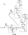
- FIG. 8A shows a schematic diagram of an exemplary design of a CA LNA 840a with a separate input attenuation circuit for each amplifier stage.
- CA LNA 840a is yet another exemplary design of CA LNA 440 in FIG. 4A .
- CA LNA 840a includes two amplifier stages 850a and 850b coupled to two input attenuation circuits 860a and 860b and to two load circuits 890a and 890b.
- An input RF signal is provided to the input of CA LNA 840a, which is node X.
- Amplifier stage 850a is coupled to node X via an NMOS transistor 842a operating as a switch, attenuation circuits 860a, and an AC coupling capacitor 844a.
- NMOS transistor 842a has its source coupled to node X, its gate receiving a first control signal, Enb1, and its drain coupled to the input of attenuation circuit 860a.
- Attenuation circuit 860a includes (i) a resistor 862a coupled between the input and output of attenuation circuit 860a and (ii) a variable resistor 864a coupled between the output of attenuation circuit 860a and circuit ground.
- AC coupling capacitor 844a is coupled between the output of attenuation circuit 860a and the input of amplifier stage 850a.
- Amplifier stage 850b is coupled to node X via an NMOS transistor 842b, an attenuation circuit 860b, and an AC coupling capacitor 844b, which are coupled in similar manner as NMOS transistor 842a, attenuation circuit 860a, and AC coupling capacitor 844a.
- Amplifier stage 850a includes a gain transistor 854a and a cascode transistor 856a.
- Gain transistor 854a has its gate coupled to AC coupling capacitor 844a and its source coupled to circuit ground (as shown in FIG. 8A ) or to a source degeneration inductor (not shown in FIG. 8A ).
- Cascode transistor 856a has its gate receiving a first bias voltage, Vcasc1, its source coupled to the drain of gain transistor 854a, and its drain coupled to load circuit 890a.
- Amplifier stage 850b includes a gain transistor 854b and a cascode transistor 856b, which are coupled in similar manner as gain transistor 854a and cascode transistor 856a.
- Amplifier stages 850a and 850b may be independently selected via NMOS transistor 842a and 842b, respectively, and independently enabled or disabled via the Vcasc1 and Vcasc2 voltages, respectively.
- FIG. 8A shows an exemplary design in which a signal path from the LNA input (node X) to each amplifier stage 850 includes NMOS transistor 842, attenuation circuit 860, and AC coupling capacitor 844.
- a signal path may also include fewer, different, and/or additional circuits.
- the signal path for amplifier stage 850a may or may not match the signal path for amplifier stage 850b.
- NMOS transistor 842a may be omitted whereas NMOS transistor 842b may be retained.
- Attenuation circuits 860a and 860b for the two signal paths may be identical, or may have the same circuit design but different values, or may have different circuit designs with different circuit topologies.
- NMOS transistor 842a operates as a switch that can pass the input RF signal to amplifier stage 850a when NMOS transistor 842a is enabled by the Enb1 signal.
- NMOS transistor 842b operates as a switch that can pass the input RF signal to amplifier stage 850b in the CA mode when NMOS transistor 842b is enabled by the Enb2 signal.
- NMOS transistors 842a may be enabled in both the CA mode and the non-CA mode, and NMOS transistors 842b may be enabled only in the CA mode.
- Separate NMOS transistors 842a and 842b and separate attenuation circuits 860a and 860b may be used to allow the input RF signal to encounter only one series switch prior to hitting gain transistor 854a or 854b.
- both NMOS transistors 842a and 842b are turned On, and the input RF signal is provided to both attenuation circuits 860a and 860b and amplifier stages 850a and 850b.
- Each amplifier stage 850 amplifies the input RF signal and provides a respective output RF signal to its load circuit 890.
- one amplifier stage 850a or 850b may be selected.
- NMOS transistor 842 for the selected amplifier stage 850 is turned On, and the input RF signal is provided to attenuation circuit 860 and the selected amplifier stage 850.
- NMOS transistor 842 for the unselected amplifier stage 850 is turned Off, and attenuation circuit 860 and the unselected amplifier stage 850 are disconnected from node X, thereby reducing loading on the signal path for the selected amplifier stage 850.
- the selected amplifier stage 850 amplifies the input RF signal and provides an output RF signal to the associated load circuit 890.
- CA LNA 840a may be advantageously used in a scenario in which the input RF signal includes jammers, which are undesired signals of large amplitude and close in frequency to the desired signals.
- Input attenuation circuits 860a and 860b may be programmable (e.g., as shown in FIG. 8A ) or may be fixed (not shown in FIG. 8A ) and may serve a dual purpose of attenuating the jammers in the input RF signal and providing a good input impedance match for CA LNA 840a.
- Attenuation circuits 860a and 860b may be designed differently and/or may have different settings/values for the CA mode and the non-CA mode in order to obtain a good input impedance match in both modes.
- FIG. 8A shows CA LNA 840a including two amplifier stages 850a and 850b for two sets of carriers.
- CA LNA 840a may include more than two amplifier stages for more than two sets of carriers.
- FIG. 8B shows a schematic diagram of an exemplary design of a CA LNA 840b with a shared input attenuation circuit for both amplifier stages 850a and 850b.
- CA LNA 840b is yet another exemplary design of CA LNA 440 in FIG. 4A .
- CA LNA 840b includes two amplifier stages 850a and 850b coupled to a shared input attenuation circuit 860a and to two load circuits 890a and 890b. Sharing input attenuation circuit 860a between amplifier stages 850a and 850b may reduce circuit area and may also provide other advantages.
- CA LNA 840b includes all of the circuit components in CA LNA 840a in FIG. 8A except for input attenuation circuit 860b and AC coupling capacitor 844b. All of the circuit components within CA LNA 840b are coupled as described above for CA LNA 840a in FIG. 8A except for NMOS transistor 842b.
- NMOS transistor 842b has its source coupled to the input of amplifier stage 850a, its gate receiving an Enb2 control signal, and its drain coupled to the input of amplifier stage 850b.
- Amplifier stages 850a and 850b may be independently selected via NMOS transistor 842a and 842b, respectively, and may be independently enabled or disabled via the Vcasc1 and Vcasc2 voltages, respectively.
- amplifier stages 850a and 850b share a common input switch implemented with NMOS transistor 842a and a common input attenuation circuit 860a.
- Input attenuation circuit 860a may be programmable (e.g., as shown in FIG. 8B ) or may be fixed (not shown in FIG. 8B ) and may serve a dual purpose of attenuating incoming jammers in the input RF signal and providing a good input impedance match for CA LNA 840b.
- Attenuation circuit 860a may have different settings for the CA mode and the non-CA mode in order to obtain a good input impedance match in both modes.
- both NMOS transistors 842a and 842b are turned On, and the input RF signal is provided via attenuation circuit 860a to both amplifier stages 850a and 850b.
- the input RF signal passes through a single series switch prior to hitting gain transistor 854a.
- the input RF signal passes through two series switches prior to hitting gain transistor 854b, which may result in a small degradation in performance of amplifier stage 850b.
- NMOS transistor 842a is turned On, and the input RF signal is provided to attenuation circuit 860a and amplifier stage 850a.
- NMOS transistor 842b is turned Off, and amplifier stage 850b is disconnected from node Y, thereby reducing capacitive loading on the signal path for amplifier stage 850a.
- the input RF signal passes through a single series switch implemented with NMOS transistor 842a prior to hitting gain transistor 854a in the non-CA mode.
- FIG. 9 shows a schematic diagram of an exemplary design of a CA LNA 940 with a tunable matching circuit.
- CA LNA 940 is another exemplary design of CA LNA 440 in FIG. 4A .
- CA LNA 940 includes two amplifier stages 950a and 950b coupled to a shared tunable matching circuit 932 and to two load circuits 990a and 990b.
- Amplifier stage 950a includes a source degeneration inductor 952a, a gain transistor 954a, and a cascode transistor 956a, which are coupled in similar manner as inductor 652a, gain transistor 654a, and cascode transistor 656a in FIG. 6A .
- Amplifier stage 950b includes a source degeneration inductor 952b, a gain transistor 954b, and a cascode transistor 956b, which are also coupled in similar manner as inductor 652a, gain transistor 654a, and cascode transistor 656a in FIG. 6A .
- Cascode transistor 956a has its gate receiving a first control voltage, Vcasc1.
- Cascode transistor 956b has its gate receiving a second control voltage, Vcasc2.
- Each amplifier stage 950 may be independently enabled or disabled based on its Vcasc control voltage.
- Amplifier stages 950a and 950b may be independently enabled or disabled via the Vcasc1 and Vcasc2 voltages, respectively.
- Matching circuit 932 receives an input RF signal and performs input matching for CA LNA 940.
- An AC coupling capacitor 944a has one end coupled to the output of matching circuit 932 and the other end coupled to the gate of gain transistor 954a.
- An AC coupling capacitor 944b has one end coupled to the output of matching circuit 932 and the other end coupled to the gate of gain transistor 954b.
- CA LNA 940 supports the CA mode and the non-CA mode.
- both amplifier stages 950a and 950b are enabled with the Vcasc1 and Vcasc2 voltages applied to cascode transistors 956a and 956b, respectively.
- the non-CA mode only one of the two amplifier stages 950a and 950b is enabled, depending on the particular load circuit to which the input RF signal is to be routed.
- Matching circuit 932 may be adjusted based on the number of enabled amplifier stages and/or which amplifier stage(s) are enabled in order to obtain good noise/power match in both the CA modes and the non-CA mode.
- MIMO LNA 540 in FIG. 5A may be implemented with various circuit architectures. Some exemplary designs of MIMO LNA 540 are described below. MIMO LNA 540 may also be implemented with transistors of various types. Some exemplary designs of MIMO LNA 540 using NMOS transistors are described below.
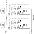
- FIG. 10 shows a schematic diagram of an exemplary design of a 2 ⁇ 2 MIMO LNA 1040 based on a cascode shutoff architecture.
- MIMO LNA 1040 is an exemplary design of MIMO LNA 540 in FIG. 5A and includes (i) two LNA inputs receiving two input RF signals, RFin1 and RFin2, and (ii) two LNA outputs providing two output RF signals, RFout1 and RFout2.
- MIMO LNA 1040 includes four amplifier stages 1050a to 1050d coupled to two load circuits 1090a and 1090b.
- Each amplifier stage 1050a includes a source degeneration inductor 1052, a gain transistor 1054, and a cascode transistor 1056, which are coupled in similar manner as inductor 652a, gain transistor 654a, and cascode transistor 656a in FIG. 6A .
- Gain transistors 1054a and 1054b within amplifier stages 1050a and 1050b have their gates receiving the first input RF signal.
- Gain transistors 1054c and 1054d within amplifier stages 1050c and 1050d have their gates receiving the second input RF signal.
- Cascode transistors 1056a and 1056c within amplifier stages 1050a and 1050c have their drains coupled to load circuit 1090a and providing the first output RF signal.
- Cascode transistors 1056b and 1056d within amplifier stages 1050b and 1050d have their drains coupled to load circuit 1090b and providing the second output RF signal.
- Amplifier stages 1050a and 1050b may be designed to provide good performance for a first set of one or more bands, e.g., as described above for CA LNA 640a in FIG. 6A .
- amplifier stages 1050c and 1050d may be designed to provide good performance for a second set of one or more bands.
- MIMO LNA 1040 may operate in a 1 ⁇ 2 configuration for intra-band CA.
- an input RF signal RFin1 or RFin2
- the input RF signal is amplified by the two gain transistors, buffered by the two cascode transistors coupled to the two gain transistors, and provided to load circuits 1090a and 1090b.
- MIMO LNA 1040 can support intra-band CA with the input RF signal provided to either of the two LNA inputs.
- MIMO LNA 1040 may operate in a 2 ⁇ 2 configuration for inter-band CA.
- a first input RF signal may be amplified by a first selected gain transistor 1054 in one amplifier stage 1050, buffered by cascode transistor 1056 coupled to the first selected gain transistor 1054, and provided to load circuit 1090a.
- a second input RF signal may be amplified by a second selected gain transistor 1054 in another amplifier stage 1050, buffered by cascode transistor 1056 coupled to the second selected gain transistor 1054, and provided to load circuit 1090b.
- FIG. 11A shows a schematic diagram of an exemplary design of a 2 ⁇ 2 MIMO LNA 1140a based on the cascode shutoff architecture.
- MIMO LNA 1140a is another exemplary design of MIMO LNA 540 in FIG. 5A and includes (i) two LNA inputs receiving two input RF signals, RFin1 and RFin2, and (ii) two LNA outputs providing two output RF signals, RFout1 and RFout2.
- MIMO LNA 1140a includes two amplifier stages 1150a and 1150b coupled to two load circuits 1190a and 1190b, respectively.
- Amplifier stage 1150a includes a source degeneration inductor 1152a, a gain transistor 1154a, and a cascode transistor 1156a, which are coupled in similar manner as inductor 652a, gain transistor 654a, and cascode transistor 656a in FIG. 6A .
- Gain transistor 1154a has its gate receiving the first input RF signal.
- Cascode transistor 1156a has its gate receiving a Vcasc1a voltage and its drain coupled to load circuit 1190a.
- Amplifier stage 1150a further includes a gain transistor 1164a and a cascode transistor 1166a.
- Gain transistor 1164a has its source coupled to inductor 1152a and its gate receiving the second input RF signal.
- Cascode transistor 1166a has its gate receiving a Vcasc2a voltage and its drain coupled to load circuit 1190a.
- Amplifier stage 1150b includes a source degeneration inductor 1152b, two gain transistors 1154b and 1164b, and two cascode transistors 1156b and 1166b, which are coupled in similar manner as inductor 1152a, gain transistors 1154a and 1164a, and cascode transistors 1156a and 1166a in amplifier stage 1150a.
- Gain transistors 1154b and 1164b have their gates receiving the first and second input RF signals, respectively.
- Cascode transistors 1156b and 1166b have their gates receiving Vcasc1b and Vcasc2b voltages, respectively, and their drains coupled to load circuit 1190b.
- MIMO LNA 1140a may operate in a 1 ⁇ 2 configuration for intra-band CA.
- an input RF signal, RFin1 or RFin2 may be provided via one LNA input to two gain transistors 1154a and 1154b (or to gain transistors 1164a and 1164b) in the two amplifier stages 1150a and 1150b.
- the input RF signal is amplified by the two gain transistors, buffered by the two cascode transistors coupled to the two gain transistors, and provided to load circuits 1190a and 1190b.
- MIMO LNA 1140a can support intra-band CA with the input RF signal applied to either of the two LNA inputs.
- MIMO LNA 1140a may operate in a 2 ⁇ 2 configuration for inter-band CA.
- a first input RF signal (e.g., RFin1) may be received by amplifier stage 1150a or 1150b and may be amplified by gain transistor 1154a or 1154b, buffered by cascode transistor 1156a or 1156b, and provided to load circuit 1190a or 1190b.
- a second input RF signal (e.g., RFin2) may be received by amplifier stage 1150a or 1150b, amplified by gain transistor 1164a or 1164b, buffered by cascode transistor 1166a or 1166b, and provided to load circuit 1190a or 1190b.
- Each amplifier stage 1150 would receive only one of the two input RF signals and would provide its output RF signal to load circuit 1190 coupled to that amplifier stage 1150.
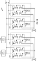
- FIG. 11B shows a schematic diagram of an exemplary design of a 4 ⁇ 2 MIMO LNA 1140b based on the cascode shutoff architecture.
- MIMO LNA 1140b is yet another exemplary design of MIMO LNA 540 in FIG. 5A and includes (i) four LNA inputs receiving four input RF signals, RFin1 to RFin4, and (ii) two LNA outputs providing two output RF signals, RFout1 and RFout2.
- MIMO LNA 1140b includes four amplifier stages 1150a to 1150d coupled to two load circuits 1190a and 1190b.
- Amplifier stages 1150a and 1150b include source degeneration inductors, gain transistors, and cascode transistors that are coupled as described above for FIG. 11A .
- Amplifier stage 1150c includes a source degeneration inductor 1152c, two gain transistors 1154c and 1164c, and two cascode transistors 1156c and 1166c, which are coupled in similar manner as inductor 1152a, gain transistors 1154a and 1164a, and cascode transistors 1156a and 1166a in amplifier stage 1150a.
- Gain transistors 1154c and 1164c have their gates receiving the third and fourth input RF signals, respectively.
- Cascode transistors 1156c and 1166c have their gates receiving Vcasc3a and Vcasc4a voltages, respectively, and their drains coupled to load circuit 1190a.
- Amplifier stage 1150d includes a source degeneration inductor 1152d, two gain transistors 1154d and 1164d, and two cascode transistors 1156d and 1166d, which are coupled in similar manner as inductor 1152a, gain transistors 1154a and 1164a, and cascode transistors 1156a and 1166a in amplifier stage 1150a.
- Gain transistors 1154d and 1164d have their gates receiving the third and fourth input RF signals, respectively.
- Cascode transistors 1156d and 1166d have their gates receiving Vcasc3b and Vcas4b voltages, respectively, and their drains coupled to load circuit 1190b.
- MIMO LNA 1140b may operate in a 1 ⁇ 2 configuration for intra-band CA.
- an input RF signal (RFin1, RFin 2, RFin3 or RFin4) may be provided via one LNA input to two gain transistors in two amplifier stages 1150.
- the input RF signal is amplified by the two gain transistors, buffered by the two cascode transistors coupled to the two gain transistors, and provided to load circuits 1190a and 1190b.
- MIMO LNA 1140b can support intra-band CA with the input RF signal applied to any one of the four LNA inputs.
- MIMO LNA 1140b may operate in a 2-input 2-output (2 ⁇ 2) configuration for inter-band CA.
- a first input RF signal (e.g., RFin1 or RFin2) may be received by amplifier stage 1150a or 1150b, amplified by a first selected gain transistor in one amplifier stage 1150a or 1150b, buffered by the cascode transistor coupled to the first selected gain transistor, and provided to load circuit 1190a or 1190b.
- a second input RF signal (e.g., RFin3 or RFin4) may be received by amplifier stage 1150c or 1150d, amplified by a second selected gain transistor in amplifier stage 1150c or 1150d, buffered by the cascode transistor coupled to the second selected gain transistor, and provided to load circuit 1190a or 1190b. Only two amplifier stages 1150 are enabled to amplify the two input RF signals. Each enabled amplifier stage 1150 would receive only one of the two input RF signals and would provide its output RF signal to load circuit 1190 coupled to that amplifier stage 1150.
- FIG. 11C shows a schematic diagram of another view of 4 ⁇ 2 MIMO LNA 1140b in FIG. 11B .
- MIMO LNA 1140b in FIG. 11C include all of the degeneration inductors, gain transistors, and cascode transistors shown in FIG. 11B , which are arranged differently in FIG. 11C.
- FIG. 11C shows that MIMO LNA 1140b can receive a single input RF signal provided to any LNA input (e.g., RFin1, RFin2, RFin3, or RFin4) and can provide two output RF signals to two load circuits 1190a and 1190b for intra-band CA.
- LNA input e.g., RFin1, RFin2, RFin3, or RFin4
- MIMO LNA 1140b can receive two input RF signals provided to two LNA inputs (e.g., RFin1 and RFin3, or RFin1 and RFin4, or RFin2 and RFin3, or RFin2 and RFin4) and can provide two output RF signals to two load circuits 1190a and 1190b for inter-band CA. If a separate source degeneration inductor is used for each gain transistor (for a total of eight source degeneration inductors), then two input RF signals may be applied to any two LNA inputs.
- FIGS. 10 and 11A show two exemplary designs of a 2 ⁇ 2 MIMO LNA.
- FIG. 11B shows an exemplary design of a 4 ⁇ 2 MIMO LNA.
- a MIMO LNA may also be implemented in other manners.
- a MIMO LNA may include one or more feedback circuits, with each feedback circuit being coupled between the input and output of one or more amplifier stages, e.g., as shown in FIG. 7 .
- a MIMO LNA with any number of inputs and any number of outputs may be implemented based on the cascode shutoff architecture. More LNA inputs for more bands may be supported with more amplifier stages and/or more gain and cascode transistors in each amplifier stage. More LNA outputs for more sets of carriers may also be supported with more amplifier stages and/or more gain and cascode transistors in each amplifier stage.
- a matching circuit and a tunable matching circuit may be implemented in various manners. Some exemplary designs of a tunable matching circuit are described below.
- FIG. 12A shows an exemplary design of a tunable matching circuit 1210 based on an L topology.
- the L topology includes a series circuit component coupled to a shunt circuit component.
- a series circuit component is a circuit component connected between two nodes.
- a shunt circuit component is a circuit component connected between a node and circuit ground.
- a circuit component may be an inductor, a capacitor, a resistor, etc.
- Matching circuit 1210 includes (i) a series inductor 1212 coupled between the input and output of matching circuit 1210 and (ii) a tunable shunt capacitor 1214 coupled between the output of matching circuit 1210 and circuit ground.
- FIG. 12B shows an exemplary design of a tunable matching circuit 1220 based on the L topology.
- Matching circuit 1220 includes (i) a tunable series capacitor 1222 coupled between the input and output of matching circuit 1220 and (ii) a shunt inductor 1224 coupled between the output of matching circuit 1220 and circuit ground.
- FIG. 12C shows an exemplary design of a tunable matching circuit 1230 based on an R topology.
- the R topology includes a shunt circuit component coupled to a series circuit component.
- Matching circuit 1230 includes (i) a tunable shunt capacitor 1232 coupled between the input of matching circuit 1230 and circuit ground and (ii) a series inductor 1234 coupled between the input and output of matching circuit 1230.
- FIG. 12D shows an exemplary design of a tunable matching circuit 1240 based on a Pi topology.
- the Pi topology includes a shunt circuit component coupled to a series circuit component, which is coupled to another shunt circuit component.
- Matching circuit 1240 includes (i) a shunt capacitor 1242 coupled between the input of matching circuit 1240 and circuit ground, (ii) a series inductor 1244 coupled between the input and output of matching circuit 1240, and (iii) a tunable shunt capacitor 1246 coupled between the output of matching circuit 1240 and circuit ground.
- FIG. 12E shows an exemplary design of a tunable matching circuit 1250 with two R sections.
- Matching circuit 1250 includes (i) a shunt inductor 1252 coupled between the input of matching circuit 1250 and a power supply, Vdd, (ii) a series capacitor 1254 coupled between the input of matching circuit 1250 and node E, (iii) a tunable shunt capacitor 1256 coupled between node E and circuit ground, and (iv) a series inductor 1258 coupled between node E and the output of matching circuit 1250.
- FIG. 12F shows an exemplary design of a tunable matching circuit 1260 based on the Pi topology.
- Matching circuit 1260 includes (i) a shunt inductor 1262 coupled between the input of matching circuit 1260 and the Vdd supply, (ii) a series capacitor 1264 coupled between the input and output of matching circuit 1260, (iii) a tunable shunt capacitor 1266 coupled between the output of matching circuit 1260 and circuit ground, and (iv) a shunt inductor 1268 coupled between the output of matching circuit 1260 and circuit ground.
- a fixed matching circuit may also be implemented based on any of the exemplary designs shown in FIGS. 12A to 12F .
- each adjustable circuit component e.g., each adjustable capacitor
- a fixed circuit component e.g., a fixed capacitor
- an apparatus may include first and second amplifier stages (e.g., for a CA LNA or a MIMO LNA).
- the first amplifier stage e.g., amplifier stage 650a in FIG. 6A
- the input RF signal may comprise transmissions sent on multiple carriers at different frequencies to a wireless device.
- the second amplifier stage e.g., amplifier stage 650b in FIG.
- Each load circuit may comprise at least one mixer (e.g., as shown in FIG. 4B or 5B ) and/or other circuits.
- the first output RF signal may be processed (e.g., downconverted) for transmissions on a first set of at least one carrier.
- the second output RF signal may be processed for transmissions on a second set of at least one carrier.
- the first amplifier stage may comprise a first gain transistor (e.g., gain transistor 654a in FIG. 6A ) coupled to a first cascode transistor (e.g., cascode transistor 656a).
- the second amplifier stage may comprise a second gain transistor (e.g., gain transistor 654b) coupled to a second cascode transistor (e.g., cascode transistor 656b).
- the input RF signal may be provided to both the first and second gain transistors.
- the first amplifier stage may further comprise a first inductor (e.g., inductor 652a) coupled to the first gain transistor.
- the second amplifier stage may further comprise a second inductor (e.g., inductor 652b) coupled to the second gain transistor.
- the first and second gain transistors may have their sources coupled to circuit ground (e.g., as shown in FIGS. 8A and 8B ).
- the first and second amplifier stages may (i) provide the first and second output RF signals in a first/CA mode and (ii) provide the first output RF signal but not the second output RF signal in a second/non-CA mode.
- the first and second cascode transistors may both be enabled in the first/CA mode. Only one of the first and second cascode transistors may be enabled in the second/non-CA mode.
- the first and second gain transistors may be applied the input RF signal in both the first/CA mode and the second/non-CA mode.
- One of the first and second gain transistors may operate in a saturation region and the other one of the first and second gain transistors may operate in a linear region in the second/non-CA mode.
- Each amplifier stage may be enabled or disabled by providing one or more appropriate voltages to one or more cascode transistors in the amplifier stage.
- a feedback circuit (e.g., feedback circuit 660 in FIG. 7 ) may be coupled between an output and an input of at least one of the first and second amplifier stages.
- the feedback circuit may comprise a resistor, or a capacitor, or an active circuit such as a transistor, or some other circuit, or any combination thereof.
- a first attenuation circuit (e.g., attenuation circuit 860a in FIG. 8A ) may be coupled to the first amplifier stage and may receive the input RF signal and provide a first attenuated input RF signal to the first amplifier stage.
- a second attenuation circuit (e.g., attenuation circuit 860b in FIG. 8A ) may be coupled to the second amplifier stage and may receive the input RF signal and provide a second attenuated input RF signal to the first amplifier stage.
- a shared/common attenuation circuit may be used for all amplifier stages, e.g., as shown in FIG. 8B .
- the share attenuation circuit (e.g., attenuation circuit 860a in FIG. 8B ) may be coupled to the first and second amplifier stages and may receive the input RF signal and provide an attenuated input RF signal to both amplifier stages.
- an input matching circuit may be used for the amplifier stages.
- the input matching circuit (e.g., input matching circuit 632 in FIG. 6A ) may be coupled to the first and second amplifier stages and may receive a receiver input signal and provide the input RF signal.
- the input matching circuit may be fixed (e.g., as shown in FIG. 6A ) and may comprise one or more fixed circuit components.
- the input matching circuit may be tunable (e.g., as shown in FIG. 9 ) and may comprise at least one adjustable circuit component.
- the apparatus may further component third and fourth amplifier stages (e.g., amplifier stages 1050c and 1050d in FIG. 10 for a MIMO LNA).
- the third amplifier stage e.g., amplifier stage 1050c
- the fourth amplifier stage may receive and amplify the second input RF signal and provide the second output RF signal to the second load circuit when the fourth amplifier stage is enabled.
- the first amplifier stage (e.g., amplifier stage 1150a in FIG. 11A ) may receive and amplify the input RF signal or a second input RF signal and may provide the first output RF signal to the first load circuit when the first amplifier stage is enabled.
- the second amplifier stage (e.g., amplifier stage 1150b) may receive and amplify the input RF signal or the second input RF signal and may provide the second output RF signal to the second load circuit when the second amplifier stage is enabled.
- the first amplifier stage may further comprise a third gain transistor (e.g., gain transistor 1164a) coupled to a third cascode transistor (e.g., cascode transistor 1166a).
- the second amplifier stage may further comprise a fourth gain transistor (e.g., gain transistor 1164b) coupled to a fourth cascode transistor (e.g., cascode transistor 1166b).
- the second input RF signal may be provided to both the third and fourth gain transistors.
- the apparatus may further include third and fourth amplifier stages (e.g., amplifier stages 1150c and 1150d in FIG. 11B for a MIMO LNA).
- the third amplifier stage e.g., amplifier stage 1150c
- the fourth amplifier stage may receive and amplify the third input RF signal or the fourth input RF signal and may provide the second output RF signal to the second load circuit when the fourth amplifier stage is enabled.
- FIG. 13 shows an exemplary design of a process 1300 for receiving signals in a wireless system.
- Process 1300 may be performed by a wireless device (as described below) or by some other entity.
- the wireless device may enable first and second amplifier stages in a first/CA mode (block 1312).
- the wireless device may enable the first amplifier stage and disable the second amplifier stage in a second/non-CA mode (block 1314).
- the wireless device may amplify a first input RF signal with the first amplifier stage to obtain a first output RF signal when the first amplifier stage is enabled (block 1316).
- the wireless device may amplify the first input RF signal or a second input RF signal with the second amplifier stage to obtain a second output RF signal when the second amplifier stage is enabled (block 1318).
- the first and second input RF signals may comprise transmissions sent on multiple carriers at different frequencies to the wireless device.
- the first and second input RF signals may be for different bands.
- the LNAs described herein may be implemented on an IC, an analog IC, an RFIC, a mixed-signal IC, an ASIC, a printed circuit board (PCB), an electronic device, etc.
- the LNAs may also be fabricated with various IC process technologies such as complementary metal oxide semiconductor (CMOS), N-channel MOS (NMOS), P-channel MOS (PMOS), bipolar junction transistor (BJT), bipolar-CMOS (BiCMOS), silicon germanium (SiGe), gallium arsenide (GaAs), heterojunction bipolar transistors (HBTs), high electron mobility transistors (HEMTs), silicon-on-insulator (SOI), etc.
- CMOS complementary metal oxide semiconductor
- NMOS N-channel MOS
- PMOS P-channel MOS
- BJT bipolar junction transistor
- BiCMOS bipolar-CMOS
- SiGe silicon germanium
- GaAs gallium arsenide
- HBTs heterojunction bipolar transistors
- An apparatus implementing the LNAs described herein may be a stand-alone device or may be part of a larger device.
- a device may be (i) a stand-alone IC, (ii) a set of one or more ICs that may include memory ICs for storing data and/or instructions, (iii) an RFIC such as an RF receiver (RFR) or an RF transmitter/receiver (RTR), (iv) an ASIC such as a mobile station modem (MSM), (v) a module that may be embedded within other devices, (vi) a receiver, cellular phone, wireless device, handset, or mobile unit, (vii) etc.
- RFR RF receiver
- RTR RF transmitter/receiver
- MSM mobile station modem
- the functions described may be implemented in hardware, software, firmware, or any combination thereof. If implemented in software, the functions may be stored on or transmitted over as one or more instructions or code on a computer-readable medium.
- Computer-readable media includes both computer storage media and communication media including any medium that facilitates transfer of a computer program from one place to another.
- a storage media may be any available media that can be accessed by a computer.
- such computer-readable media can comprise RAM, ROM, EEPROM, CD-ROM or other optical disk storage, magnetic disk storage or other magnetic storage devices, or any other medium that can be used to carry or store desired program code in the form of instructions or data structures and that can be accessed by a computer.
- any connection is properly termed a computer-readable medium.
- the software is transmitted from a website, server, or other remote source using a coaxial cable, fiber optic cable, twisted pair, digital subscriber line (DSL), or wireless technologies such as infrared, radio, and microwave
- the coaxial cable, fiber optic cable, twisted pair, DSL, or wireless technologies such as infrared, radio, and microwave are included in the definition of medium.
- Disk and disc includes compact disc (CD), laser disc, optical disc, digital versatile disc (DVD), floppy disk and blu-ray disc where disks usually reproduce data magnetically, while discs reproduce data optically with lasers. Combinations of the above should also be included within the scope of computer-readable media.
Applications Claiming Priority (3)
| Application Number | Priority Date | Filing Date | Title |
|---|---|---|---|
| US201261652064P | 2012-05-25 | 2012-05-25 | |
| US13/590,423 US9154356B2 (en) | 2012-05-25 | 2012-08-21 | Low noise amplifiers for carrier aggregation |
| PCT/US2013/042726 WO2013177555A1 (en) | 2012-05-25 | 2013-05-24 | Low noise amplifiers for carrier aggregation |
Publications (2)
| Publication Number | Publication Date |
|---|---|
| EP2856639A1 EP2856639A1 (en) | 2015-04-08 |
| EP2856639B1 true EP2856639B1 (en) | 2019-09-11 |
Family
ID=49621593
Family Applications (4)
| Application Number | Title | Priority Date | Filing Date |
|---|---|---|---|
| EP13727013.8A Active EP2856640B1 (en) | 2012-05-25 | 2013-05-24 | Low noise amplifiers with cascode divert switch for carrier aggregation |
| EP13728071.5A Active EP2856638B1 (en) | 2012-05-25 | 2013-05-24 | Low noise amplifiers with transformer-based signal splitting for carrier aggregation |
| EP13728878.3A Active EP2856639B1 (en) | 2012-05-25 | 2013-05-24 | Low noise amplifiers for carrier aggregation |
| EP13728607.6A Active EP2856641B1 (en) | 2012-05-25 | 2013-05-24 | Multiple-input multiple-output (mimo) low noise amplifiers for carrier aggregation |
Family Applications Before (2)
| Application Number | Title | Priority Date | Filing Date |
|---|---|---|---|
| EP13727013.8A Active EP2856640B1 (en) | 2012-05-25 | 2013-05-24 | Low noise amplifiers with cascode divert switch for carrier aggregation |
| EP13728071.5A Active EP2856638B1 (en) | 2012-05-25 | 2013-05-24 | Low noise amplifiers with transformer-based signal splitting for carrier aggregation |
Family Applications After (1)
| Application Number | Title | Priority Date | Filing Date |
|---|---|---|---|
| EP13728607.6A Active EP2856641B1 (en) | 2012-05-25 | 2013-05-24 | Multiple-input multiple-output (mimo) low noise amplifiers for carrier aggregation |
Country Status (9)
| Country | Link |
|---|---|
| US (4) | US9154356B2 (zh) |
| EP (4) | EP2856640B1 (zh) |
| JP (3) | JP6522497B2 (zh) |
| KR (3) | KR102160715B1 (zh) |
| CN (6) | CN106982032B (zh) |
| BR (1) | BR112014029217A2 (zh) |
| ES (1) | ES2755030T3 (zh) |
| HU (1) | HUE045213T2 (zh) |
| WO (4) | WO2013177555A1 (zh) |
Families Citing this family (122)
| Publication number | Priority date | Publication date | Assignee | Title |
|---|---|---|---|---|
| US9026070B2 (en) | 2003-12-18 | 2015-05-05 | Qualcomm Incorporated | Low-power wireless diversity receiver with multiple receive paths |
| US9450665B2 (en) | 2005-10-19 | 2016-09-20 | Qualcomm Incorporated | Diversity receiver for wireless communication |
| US9178669B2 (en) | 2011-05-17 | 2015-11-03 | Qualcomm Incorporated | Non-adjacent carrier aggregation architecture |
| US9252827B2 (en) | 2011-06-27 | 2016-02-02 | Qualcomm Incorporated | Signal splitting carrier aggregation receiver architecture |
| US9154179B2 (en) | 2011-06-29 | 2015-10-06 | Qualcomm Incorporated | Receiver with bypass mode for improved sensitivity |
| US8774334B2 (en) | 2011-11-09 | 2014-07-08 | Qualcomm Incorporated | Dynamic receiver switching |
| JP6041498B2 (ja) * | 2012-02-03 | 2016-12-07 | 株式会社Nttドコモ | 移動通信方法、無線基地局及び移動局 |
| US9362958B2 (en) | 2012-03-02 | 2016-06-07 | Qualcomm Incorporated | Single chip signal splitting carrier aggregation receiver architecture |
| US9172402B2 (en) | 2012-03-02 | 2015-10-27 | Qualcomm Incorporated | Multiple-input and multiple-output carrier aggregation receiver reuse architecture |
| US9118439B2 (en) | 2012-04-06 | 2015-08-25 | Qualcomm Incorporated | Receiver for imbalanced carriers |
| US9154356B2 (en) | 2012-05-25 | 2015-10-06 | Qualcomm Incorporated | Low noise amplifiers for carrier aggregation |
| US9867194B2 (en) | 2012-06-12 | 2018-01-09 | Qualcomm Incorporated | Dynamic UE scheduling with shared antenna and carrier aggregation |
| US9300420B2 (en) | 2012-09-11 | 2016-03-29 | Qualcomm Incorporated | Carrier aggregation receiver architecture |
| US9543903B2 (en) | 2012-10-22 | 2017-01-10 | Qualcomm Incorporated | Amplifiers with noise splitting |
| US9603187B2 (en) | 2012-11-14 | 2017-03-21 | Qualcomm Incorporated | Omni-band amplifiers |
| WO2014125325A1 (en) * | 2013-02-12 | 2014-08-21 | Freescale Semiconductor, Inc. | Active iq and quadrature generator for high frequency applications |
| US8995591B2 (en) | 2013-03-14 | 2015-03-31 | Qualcomm, Incorporated | Reusing a single-chip carrier aggregation receiver to support non-cellular diversity |
| US9035697B2 (en) * | 2013-03-15 | 2015-05-19 | Qualcomm Incorporated | Split amplifiers with improved linearity |
| US20150004922A1 (en) * | 2013-06-27 | 2015-01-01 | Samsung Electronics Co., Ltd. | Modulation circuit and wireless communication apparatus |
| US8929945B1 (en) * | 2013-07-18 | 2015-01-06 | Mstar Semiconductor, Inc. | Transceivers with a transformer supporting multiband operation |
| EP3033836B8 (en) * | 2013-08-16 | 2018-11-14 | Telefonaktiebolaget LM Ericsson (publ) | Radio receiver circuit, communication apparatus, and adaptation method |
| US9263998B2 (en) * | 2013-12-16 | 2016-02-16 | Mstar Semiconductor, Inc. | Broadband single-ended input to differential output low-noise amplifier |
| US20150180694A1 (en) * | 2013-12-19 | 2015-06-25 | Nvidia Corporation | Radio frequency circuit for intra-band and inter-band carrier aggregation |
| US9178473B2 (en) * | 2013-12-19 | 2015-11-03 | Qualcomm Incorporated | Distortion cancellation for low noise amplifier (LNA) non-linear second order products |
| US9270303B2 (en) * | 2013-12-30 | 2016-02-23 | Broadcom Corporation | Configurable receiver architecture for carrier aggregation with multiple-input multiple-output |
| US9425832B2 (en) | 2014-01-16 | 2016-08-23 | Qualcomm Incorporated | Inter carrier-aggregation isolation in a receiver |
| US9319007B2 (en) * | 2014-01-30 | 2016-04-19 | National Taiwan University | Three-dimensional power amplifier architecture |
| US9271239B2 (en) * | 2014-02-14 | 2016-02-23 | Qualcomm Incorporated | Current-efficient low noise amplifier (LNA) |
| EP2913922A1 (en) * | 2014-02-28 | 2015-09-02 | Telefonaktiebolaget L M Ericsson (publ) | A low noise amplifier circuit |
| US9413406B2 (en) * | 2014-03-14 | 2016-08-09 | Qualcomm Incorporated | Single input multiple-output power amplifier |
| US9374042B2 (en) | 2014-03-27 | 2016-06-21 | Infineon Technologies Ag | System and method for a low noise amplifier |
| US9467104B2 (en) * | 2014-03-28 | 2016-10-11 | Qualcomm Incorporated | Single-input multiple-output amplifiers with simultaneous multiple gain modes |
| US9425746B2 (en) * | 2014-03-28 | 2016-08-23 | Qualcomm Incorporated | Spurious signal mitigation for carrier aggregation amplifier |
| GB2591952B (en) * | 2014-04-11 | 2021-12-29 | Skyworks Solutions Inc | Circuits and methods related to switchless carrier aggregation in radio-frequency receivers |
| US9723560B2 (en) * | 2014-05-22 | 2017-08-01 | Qualcomm Incorporated | Multi-stage amplifier with RC network |
| US9479131B2 (en) | 2014-05-23 | 2016-10-25 | Qualcomm Incorporated | Carrier aggregation amplifier with dual gain control |
| US9525503B2 (en) | 2014-05-28 | 2016-12-20 | Qualcomm Incorporated | Reconfigurable multi-mode transceiver |
| US9642166B2 (en) * | 2014-05-29 | 2017-05-02 | Qualcomm Incorporated | Cross-connected cascode low noise amplifier for carrier aggregation |
| US9379673B2 (en) | 2014-05-30 | 2016-06-28 | Qualcomm Incorporated | Distortion cancellation for dual stage carrier-aggregation (CA) low noise amplifier (LNA) non-linear second order products |
| GB2529309B (en) * | 2014-07-14 | 2021-03-17 | Skyworks Solutions Inc | Circuits and devices related to fast turn-on of radio-frequency amplifiers |
| KR102301680B1 (ko) * | 2014-07-16 | 2021-09-14 | 삼성전자주식회사 | 다이버시티 증폭 모듈 및 이를 포함하는 전자 장치 |
| EP2978130B1 (en) | 2014-07-24 | 2019-09-11 | Renesas Electronics Europe GmbH | Circuit for controlling slew rate of a high-side switching element |
| US20160036392A1 (en) * | 2014-07-30 | 2016-02-04 | Qualcomm Incorporated | Dual-band amplifier |
| KR102196752B1 (ko) * | 2014-08-12 | 2020-12-30 | 삼성전자주식회사 | 캐리어 통합 신호를 송수신하는 장치 |
| US9479126B2 (en) * | 2014-08-19 | 2016-10-25 | Infineon Technologies Ag | System and method for a low noise amplifier |
| SG11201701512YA (en) | 2014-08-29 | 2017-03-30 | Skyworks Solutions Inc | Domino circuit and related architectures and methods for carrier aggregation |
| US9431963B2 (en) | 2014-09-19 | 2016-08-30 | Qualcomm Incorporated | Dual stage low noise amplifier for multiband receiver |
| US9385901B2 (en) | 2014-11-13 | 2016-07-05 | Qualcomm Incorporated | Receiver front end architecture for intra band carrier aggregation |
| US9641139B2 (en) * | 2014-11-17 | 2017-05-02 | Mediatek Inc. | Amplifier and related method |
| US9831838B2 (en) | 2014-12-16 | 2017-11-28 | Nvidia Corporation | Low noise amplifier architecture for carrier aggregation receivers |
| US20160173145A1 (en) * | 2014-12-16 | 2016-06-16 | Nvidia Corporation | Low noise amplifier providing variable gains and noise cancellation for carrier aggregation |
| US9407205B2 (en) | 2014-12-23 | 2016-08-02 | Macom Technology Solutions Holdings, Inc. | Double down-conversion with multiple independent intermediate frequencies for E-band applications |
| US9712117B2 (en) | 2014-12-30 | 2017-07-18 | Skyworks Solutions, Inc. | Cascode switch for power amplifier |
| KR102384866B1 (ko) * | 2015-01-13 | 2022-04-08 | 삼성전자주식회사 | 수신기, 무선 단말 및 무선 단말의 동작 방법 |
| US10009201B2 (en) | 2015-01-13 | 2018-06-26 | Samsung Electronics Co., Ltd | Receiver and wireless terminal for signal processing |
| US20160218852A1 (en) * | 2015-01-22 | 2016-07-28 | Qualcomm Incorporated | Half-duplex sawless receiver |
| US9589916B2 (en) * | 2015-02-10 | 2017-03-07 | Infineon Technologies Ag | Inductively coupled transformer with tunable impedance match network |
| US10187023B2 (en) * | 2015-02-15 | 2019-01-22 | Skyworks Solutions, Inc. | Power amplifier with cascode switching or splitting functionality |
| US10211861B2 (en) | 2015-03-17 | 2019-02-19 | Skyworks Solutions, Inc. | Multi-mode integrated front end module |
| HUE047986T2 (hu) * | 2015-03-31 | 2020-05-28 | Ericsson Telefon Ab L M | Rádiófrekvencia-sávok sokaságának vétele |
| US9515749B2 (en) * | 2015-05-07 | 2016-12-06 | Qualcomm Incorporated | Low noise amplifier module with output coupler |
| US9712195B2 (en) | 2015-05-13 | 2017-07-18 | Qualcomm Incorporated | Radio frequency low noise amplifier with on-chip matching and built-in tunable filter |
| CN104935287B (zh) * | 2015-06-26 | 2018-01-30 | 英特尔公司 | 射频接收器及其电感耦合单端输入差分输出低噪声放大器 |
| CN105099492B (zh) * | 2015-07-28 | 2017-12-29 | 联想(北京)有限公司 | 一种电子设备及其控制方法 |
| US9774303B1 (en) * | 2015-08-25 | 2017-09-26 | Marvell International Ltd. | Low-noise amplifier for intra-band non contiguous carrier agregation |
| US9755678B2 (en) | 2015-12-01 | 2017-09-05 | Analog Devices Global | Low noise transconductance amplifiers |
| US9712113B2 (en) | 2015-12-01 | 2017-07-18 | Analog Devices Global | Local oscillator paths |
| US10608600B2 (en) * | 2015-12-23 | 2020-03-31 | Analog Devices, Inc | Adaptable receiver amplifier |
| CN109155609B (zh) * | 2016-01-06 | 2020-06-02 | Avx安泰纳股份有限公司 | 无记忆共模不敏感的和低牵引的压控振荡器 |
| US10177722B2 (en) | 2016-01-12 | 2019-01-08 | Qualcomm Incorporated | Carrier aggregation low-noise amplifier with tunable integrated power splitter |
| US10033338B2 (en) * | 2016-06-17 | 2018-07-24 | Qualcomm Incorporated | Switched inductor/transformer for dual-band low-noise amplifier (LNA) |
| US10033337B2 (en) | 2016-08-09 | 2018-07-24 | Qualcomm Incorporated | Multi-stage bandpass low-noise amplifier |
| CN109845098B (zh) * | 2016-08-31 | 2024-02-13 | 天工方案公司 | 具有退化开关块和低损耗旁路功能的多输入放大器 |
| JP6623133B2 (ja) | 2016-09-05 | 2019-12-18 | 株式会社東芝 | 高周波半導体増幅回路 |
| US9774302B1 (en) | 2016-09-27 | 2017-09-26 | Globalfoundries Inc. | Amplifier circuit with single-ended input and differential outputs |
| US10250195B2 (en) | 2016-11-18 | 2019-04-02 | Samsung Electronics Co., Ltd. | Receiver receiving wideband radio frequency signal, wireless communication device including the same, and method of operating the wireless communication device |
| US10516432B2 (en) | 2016-12-01 | 2019-12-24 | Mediatek Inc. | Communication system with switchable devices |
| US10411658B2 (en) | 2016-12-14 | 2019-09-10 | Kabushiki Kaisha Toshiba | Semiconductor device |
| US10122332B2 (en) | 2016-12-14 | 2018-11-06 | Qualcomm Incorporated | Low-noise amplifier with integrated wideband transformer-based power splitter |
| KR20180070328A (ko) | 2016-12-16 | 2018-06-26 | 삼성전자주식회사 | 반송파 집성을 위한 저잡음 증폭기 및 이를 포함하는 장치 |
| KR102534861B1 (ko) * | 2016-12-23 | 2023-05-22 | 삼성전자주식회사 | 앰프 모듈 및 그 제어 방법 |
| US10033340B1 (en) * | 2017-01-06 | 2018-07-24 | Qualcomm Incorporated | Low-noise amplifier (LNA) with capacitive attenuator |
| US9800273B1 (en) | 2017-03-01 | 2017-10-24 | Qualcomm Incorporated | Wideband high linearity LNA with intra-band carrier aggregation support |
| US10038418B1 (en) * | 2017-04-04 | 2018-07-31 | Psemi Corporation | Optimized multi gain LNA enabling low current and high linearity including highly linear active bypass |
| US11881828B2 (en) | 2017-04-04 | 2024-01-23 | Psemi Corporation | Tunable effective inductance for multi-gain LNA with inductive source degeneration |
| JP6761374B2 (ja) | 2017-05-25 | 2020-09-23 | 株式会社東芝 | 半導体装置 |
| CN109412537B (zh) * | 2017-08-15 | 2022-10-14 | 诺基亚通信公司 | 低噪声放大器保护 |
| CN109429303B (zh) * | 2017-08-30 | 2021-01-15 | 中国移动通信有限公司研究院 | 一种网络搜索方法、终端和计算机可读存储介质 |
| EP3451530A1 (en) * | 2017-08-30 | 2019-03-06 | MediaTek Inc. | Transformer or inductor sharing in a radio frequency amplifier and method therefor |
| CN107888153A (zh) * | 2017-10-20 | 2018-04-06 | 江苏卓胜微电子股份有限公司 | 一种低噪声放大器和利用低噪声放大器的射频放大方法 |
| CN107809259B (zh) * | 2017-11-09 | 2019-09-06 | 广东凯亨信息科技有限公司 | 一种无线信号增强装置 |
| US10965261B2 (en) * | 2017-12-05 | 2021-03-30 | Qualcomm Incorporated | Power amplifier circuit |
| CN112042116A (zh) * | 2018-03-30 | 2020-12-04 | 苹果公司 | 支持多载波操作的低噪声放大器 |
| KR102468797B1 (ko) * | 2018-04-04 | 2022-11-18 | 삼성전자주식회사 | 반송파 집성을 지원하기 위한 증폭 동작을 수행하는 rf 집적회로 및 이를 포함하는 수신기 |
| US10855317B2 (en) | 2018-04-05 | 2020-12-01 | Swiftlink Technologies Inc. | Broadband receiver for multi-band millimeter-wave wireless communication |
| KR20190124448A (ko) * | 2018-04-26 | 2019-11-05 | 삼성전기주식회사 | 캐리어 어그리게이션(ca) 지원 가능한 멀티 입력 및 출력 구조를 갖는 저잡음 증폭회로 |
| JP6951293B2 (ja) * | 2018-05-29 | 2021-10-20 | 株式会社東芝 | 半導体装置 |
| US10707817B2 (en) * | 2018-05-30 | 2020-07-07 | Speedlink Technology Inc. | Wideband low noise amplifier (LNA) with a reconfigurable bandwidth for millimeter-wave 5G communication |
| US11251880B2 (en) | 2018-07-19 | 2022-02-15 | Futurewei Technologies, Inc. | CA power measurement |
| JP2020017812A (ja) * | 2018-07-24 | 2020-01-30 | 日本電気株式会社 | 増幅器 |
| CN110957980B (zh) * | 2018-09-27 | 2023-06-20 | 天津大学青岛海洋技术研究院 | 一种基于SiGe工艺的毫米波有源正交信号发生器 |
| US10574287B1 (en) * | 2018-09-28 | 2020-02-25 | Qualcomm Incorporated | Wireless transceiver with reconfigurable transformers |
| TWI672903B (zh) * | 2018-10-03 | 2019-09-21 | 立積電子股份有限公司 | 放大器電路 |
| KR102463983B1 (ko) | 2018-12-26 | 2022-11-07 | 삼성전자 주식회사 | 누설 전류를 차단하기 위한 증폭기 및 상기 증폭기를 포함하는 전자 장치 |
| JP7185548B2 (ja) * | 2019-02-07 | 2022-12-07 | 株式会社東芝 | 高周波増幅回路 |
| US10771025B1 (en) * | 2019-02-19 | 2020-09-08 | Psemi Corporation | RFFE LNA topology supporting both noncontiguous intraband carrier aggregation and interband carrier aggregation |
| KR20210148351A (ko) * | 2019-04-19 | 2021-12-07 | 스위프트링크 테크놀로지스 컴퍼니 리미티드 | 다중-대역 밀리미터파 무선 통신을 위한 광대역 수신기 |
| KR20210015333A (ko) | 2019-08-01 | 2021-02-10 | 삼성전자주식회사 | 복수의 전압 레귤레이터들을 포함하는 전자 시스템 |
| US11283409B2 (en) | 2019-08-30 | 2022-03-22 | Qualcomm Incorporated | Signal combiner |
| KR20210031169A (ko) | 2019-09-11 | 2021-03-19 | 삼성전자주식회사 | 수신기 회로 및 수신시스템 |
| US11139791B2 (en) * | 2019-09-18 | 2021-10-05 | Texas Instruments Incorporated | Integrated circuit devices with receiver chain peak detectors |
| KR102653889B1 (ko) * | 2019-10-18 | 2024-04-02 | 삼성전자주식회사 | 반송파 집성을 지원하는 수신기 및 이를 포함하는 무선 통신 장치 |
| WO2021090984A1 (ko) * | 2019-11-07 | 2021-05-14 | 엘지전자 주식회사 | 이중 연결을 지원하는 전자기기 및 그 전자기기의 제어 방법 |
| CN114731139A (zh) * | 2019-11-29 | 2022-07-08 | 华为技术有限公司 | 一种射频接收机 |
| KR102105382B1 (ko) * | 2020-01-23 | 2020-04-28 | 삼성전기주식회사 | 캐리어 어그리게이션(ca) 지원 가능한 멀티 입력 및 출력 구조를 갖는 저잡음 증폭회로 |
| US20210314016A1 (en) | 2020-04-05 | 2021-10-07 | Skyworks Solutions, Inc. | Switching circuits for bridge combiners |
| JP2022011971A (ja) * | 2020-06-30 | 2022-01-17 | 株式会社村田製作所 | 高周波モジュール及び通信装置 |
| US11159191B1 (en) * | 2020-09-11 | 2021-10-26 | Apple Inc. | Wireless amplifier circuitry for carrier aggregation |
| US11095334B1 (en) * | 2020-09-22 | 2021-08-17 | Apple Inc. | Amplifier circuitry for carrier aggregation |
| CN115882793A (zh) * | 2021-09-22 | 2023-03-31 | 深圳市中兴微电子技术有限公司 | 功率放大装置和发射机 |
| US20230097399A1 (en) * | 2021-09-24 | 2023-03-30 | Qualcomm Incorporated | High linearity modes in wireless receivers |
| US20230387863A1 (en) * | 2022-05-27 | 2023-11-30 | Psemi Corporation | Feedback topologies for amplifier gain reduction |
Family Cites Families (329)
| Publication number | Priority date | Publication date | Assignee | Title |
|---|---|---|---|---|
| US3911364A (en) | 1974-05-09 | 1975-10-07 | Bell Telephone Labor Inc | Cophasing combiner with cochannel signal selector |
| JPS5542790B2 (zh) | 1975-01-09 | 1980-11-01 | ||
| US4035729A (en) | 1976-05-21 | 1977-07-12 | General Electric Company | Audio signal quality indicating circuit |
| GB1588367A (en) | 1977-10-18 | 1981-04-23 | Parker B D | Apparatus for selecting one of a plurality of receivers receiving a signal from a single common source |
| US4326294A (en) | 1979-02-13 | 1982-04-20 | Nippon Telegraph & Telephone Public Corporation | Space diversity reception system having compensation means of multipath effect |
| JPS61284125A (ja) | 1985-06-11 | 1986-12-15 | Nec Corp | ダイバ−シチ受信方式 |
| JPH0683127B2 (ja) | 1985-07-22 | 1994-10-19 | 日本電気株式会社 | ダイバーシチ受信無線機 |
| US4715048A (en) | 1986-05-02 | 1987-12-22 | Canadian Patents And Development Limited | Frequency offset diversity receiving system |
| US4969207A (en) | 1987-03-20 | 1990-11-06 | Nippon Telegraph And Telephone Corporation | Radio receiver with reception deterioration compensation |
| JPH054352Y2 (zh) * | 1987-07-22 | 1993-02-03 | ||
| GB8821570D0 (en) | 1988-09-15 | 1989-03-30 | Plessey Co Plc | Course recommendation display |
| JPH03214930A (ja) * | 1990-01-19 | 1991-09-20 | Matsushita Electric Ind Co Ltd | テレビジョン信号切替装置 |
| US5390342A (en) | 1990-03-14 | 1995-02-14 | Pioneer Electronic Corporation | Receiver using selective diversity receiving system |
| JP2643614B2 (ja) | 1991-02-22 | 1997-08-20 | 日本電気株式会社 | ディジタル移動通信端末装置 |
| US5128630A (en) | 1991-05-03 | 1992-07-07 | Motorola, Inc. | High speed fully differential operational amplifier |
| JPH05102898A (ja) | 1991-08-07 | 1993-04-23 | Shiyoudenriyoku Kosoku Tsushin Kenkyusho:Kk | 高調波通信方式 |
| US5321850A (en) | 1991-10-09 | 1994-06-14 | Telefonaktiebolaget L M Ericsson | Diversity radio receiver automatic frequency control |
| JP3301102B2 (ja) | 1992-02-14 | 2002-07-15 | ソニー株式会社 | 受信装置 |
| KR0143039B1 (ko) | 1993-02-26 | 1998-08-01 | 사토 후미오 | 다이버시티 수신기 |
| JPH0730452A (ja) | 1993-07-12 | 1995-01-31 | Fujitsu Ltd | 受信回路 |
| JP3250693B2 (ja) * | 1993-07-21 | 2002-01-28 | 日本電信電話株式会社 | 出力切替増幅装置 |
| US5541963A (en) | 1993-12-01 | 1996-07-30 | Hitachi, Ltd. | Diversity receiving apparatus |
| US5566364A (en) | 1994-01-31 | 1996-10-15 | Nec Corporation | Power saving portable radio communication device with diversity reception |
| JPH07221684A (ja) | 1994-02-09 | 1995-08-18 | Hitachi Ltd | 移動体通信の無線端末装置 |
| JP3022194B2 (ja) | 1994-09-02 | 2000-03-15 | 三菱電機株式会社 | ダイバーシチ受信装置 |
| US5694395A (en) | 1994-09-30 | 1997-12-02 | Lucent Technologies, Inc. | Method and apparatus for processing multicarrier signals |
| JP3088246B2 (ja) | 1994-10-05 | 2000-09-18 | 三菱電機株式会社 | 無線通信装置 |
| GB9424341D0 (en) | 1994-12-02 | 1995-01-18 | Philips Electronics Uk Ltd | Receiver diversity |
| WO1996018249A1 (fr) * | 1994-12-05 | 1996-06-13 | Ntt Mobile Communications Network Inc. | Appareil et procede pour multiplexer un signal |
| JP3183812B2 (ja) | 1995-10-16 | 2001-07-09 | 株式会社エヌ・ティ・ティ・ドコモ | 移動無線機のマルチバンド高周波回路 |
| US5940452A (en) | 1995-11-29 | 1999-08-17 | Motorola, Inc. | Dual mode radio subscriber unit having a diversity receiver apparatus and method therefor |
| JPH09200070A (ja) | 1996-01-12 | 1997-07-31 | Matsushita Electric Ind Co Ltd | 受信回路 |
| DE19630280A1 (de) | 1996-07-26 | 1998-01-29 | Basf Ag | Verfahren zur Herstellung von Cokondensaten aus Asparaginsäure und Aminen |
| US5794159A (en) | 1996-08-07 | 1998-08-11 | Nokia Mobile Phones Limited | Dual band mobile station employing cross-connected transmitter and receiver circuits |
| US6026288A (en) | 1996-12-10 | 2000-02-15 | Lucent Technologies, Inc. | Communications system with an apparatus for controlling overall power consumption based on received signal strength |
| JP3657377B2 (ja) | 1996-12-27 | 2005-06-08 | 松下電器産業株式会社 | 受信回路 |
| FI108486B (fi) | 1997-01-31 | 2002-01-31 | Nokia Corp | Menetelmõ ja piirijõrjestely vastaanotettujen signaalien kõsittelemiseksi tiedonsiirtojõrjestelmõssõ |
| US6040732A (en) | 1997-04-09 | 2000-03-21 | Analog Devices, Inc. | Switched-transconductance circuit within integrated T-switches |
| CN1135763C (zh) * | 1997-07-31 | 2004-01-21 | 松下电器产业株式会社 | 正交频分复用信号解调装置 |
| JPH11127300A (ja) | 1997-10-22 | 1999-05-11 | Canon Inc | 無線通信装置および方法 |
| DE19802373C1 (de) | 1998-01-22 | 1999-06-17 | Siemens Ag | Schaltung zur Demodulation von durch geträgerte Datenübertragung gesendeten zweidimensionalen Datensymbolen |
| JP3109504B2 (ja) | 1998-03-27 | 2000-11-20 | 日本電気株式会社 | セルラシステムおよびセルラシステムの隣接周波数干渉回避方法と移動局 |
| US5999990A (en) | 1998-05-18 | 1999-12-07 | Motorola, Inc. | Communicator having reconfigurable resources |
| EP0959567A1 (en) * | 1998-05-19 | 1999-11-24 | Robert Bosch Gmbh | Diplexer for mobile phone |
| JP2000013278A (ja) | 1998-06-25 | 2000-01-14 | Matsushita Electric Ind Co Ltd | 無線装置及びそれを備える無線携帯機及び無線基地局並びにそれらを含む無線通信システム |
| US5999815A (en) | 1998-07-08 | 1999-12-07 | Motorola, Inc. | Method and apparatus for implementing diversity for a dual-mode communication unit |
| US6088348A (en) | 1998-07-13 | 2000-07-11 | Qualcom Incorporated | Configurable single and dual VCOs for dual- and tri-band wireless communication systems |
| JP3109595B2 (ja) | 1998-08-28 | 2000-11-20 | 日本電気株式会社 | 受信ダイバーシティ制御方法およびダイバーシティ受信機 |
| DE19845534B4 (de) | 1998-10-02 | 2005-01-27 | Robert Bosch Gmbh | Antennenschaltung |
| JP3199039B2 (ja) | 1998-11-02 | 2001-08-13 | 日本電気株式会社 | 消費電力低減回路及びこれを用いた無線通信装置並びに無線通信装置における消費電力低減方法 |
| US6879816B2 (en) | 1998-11-12 | 2005-04-12 | Broadcom Corporation | Integrated switchless programmable attenuator and low noise amplifier |
| US6430237B1 (en) | 1998-11-16 | 2002-08-06 | Transamerica Business Credit Corporation | Method for accurate signal-to-interference measurement for wireless communication receivers |
| GB2347596B (en) | 1998-12-18 | 2003-07-30 | Mitel Corp | Apparatus for estimating jitter in RTP encapsulated voice packets received over a data network |
| US6522895B1 (en) | 1998-12-31 | 2003-02-18 | Ericsson Inc. | Integrated transmitter and receiver components for a dual-band transceiver |
| US6208844B1 (en) | 1999-02-23 | 2001-03-27 | Conexant Systems, Inc. | System and process for shared functional block communication transceivers with GPS capability |
| KR20010002982A (ko) * | 1999-06-19 | 2001-01-15 | 김영석 | 매칭회로를 내장한 저잡음증폭기 |
| US7123891B2 (en) | 1999-06-28 | 2006-10-17 | Skyworks Solutions, Inc. | Wireless communications device allowing a soft handoff procedure in a mobile communications system |
| US6377117B2 (en) * | 1999-07-27 | 2002-04-23 | Conexant Systems, Inc. | Method and system for efficiently transmitting energy from an RF device |
| US7260369B2 (en) | 2005-08-03 | 2007-08-21 | Kamilo Feher | Location finder, tracker, communication and remote control system |
| US6684065B2 (en) | 1999-12-20 | 2004-01-27 | Broadcom Corporation | Variable gain amplifier for low voltage applications |
| CN1132344C (zh) | 2000-01-04 | 2003-12-24 | 三菱电机株式会社 | 便携式电话机 |
| AU2001249730A1 (en) | 2000-03-28 | 2001-10-08 | California Institute Of Technology | Concurrent multi-band low noise amplifier architecture |
| JP2001285114A (ja) | 2000-03-28 | 2001-10-12 | Sharp Corp | アンテナ共用複数バンド通信機 |
| JP2002118483A (ja) | 2000-10-11 | 2002-04-19 | Matsushita Electric Ind Co Ltd | 無線回路装置及び無線回路装置の制御方法 |
| US6407689B1 (en) | 2000-11-01 | 2002-06-18 | Qualcomm, Incorporated | Method and apparatus for controlling stages of a multi-stage circuit |
| US6694129B2 (en) | 2001-01-12 | 2004-02-17 | Qualcomm, Incorporated | Direct conversion digital domain control |
| JP2002261880A (ja) | 2001-02-28 | 2002-09-13 | Sanyo Electric Co Ltd | 携帯電話機 |
| AU2002231210A1 (en) | 2001-03-14 | 2002-10-03 | California Institute Of Technology | Concurrent dual-band receiver architecture |
| US6424222B1 (en) | 2001-03-29 | 2002-07-23 | Gct Semiconductor, Inc. | Variable gain low noise amplifier for a wireless terminal |
| US6600931B2 (en) | 2001-03-30 | 2003-07-29 | Nokia Corporation | Antenna switch assembly, and associated method, for a radio communication station |
| US6535725B2 (en) | 2001-03-30 | 2003-03-18 | Skyworks Solutions, Inc. | Interference reduction for direct conversion receivers |
| US20020193108A1 (en) | 2001-05-10 | 2002-12-19 | Robinett Robert L. | Multi-mode satellite and terrestrial communication device with position location |
| FI20011217A (fi) | 2001-06-08 | 2002-12-09 | Nokia Corp | Vastaanottomenetelmä, radiojärjestelmä ja vastaanotin |
| US7024172B1 (en) | 2001-06-15 | 2006-04-04 | Rockwell Collins, Inc. | Direct conversion receiver using a dithered local oscillator to mitigate adjacent channel coherent interference |
| US6888888B1 (en) | 2001-06-26 | 2005-05-03 | Microsoft Corporation | Simultaneous tuning of multiple channels using intermediate frequency sub-sampling |
| US6985712B2 (en) | 2001-08-27 | 2006-01-10 | Matsushita Electric Industrial Co., Ltd. | RF device and communication apparatus using the same |
| US7061993B2 (en) | 2001-08-29 | 2006-06-13 | Sony Corporation | CDMA receiver architecture for lower bypass switch point |
| US7277679B1 (en) | 2001-09-28 | 2007-10-02 | Arraycomm, Llc | Method and apparatus to provide multiple-mode spatial processing to a terminal unit |
| US6819941B2 (en) | 2001-10-11 | 2004-11-16 | Rf Micro Devices, Inc. | Single output stage power amplification for multimode applications |
| US7116652B2 (en) | 2001-10-18 | 2006-10-03 | Lucent Technologies Inc. | Rate control technique for layered architectures with multiple transmit and receive antennas |
| US20030125040A1 (en) | 2001-11-06 | 2003-07-03 | Walton Jay R. | Multiple-access multiple-input multiple-output (MIMO) communication system |
| US6754510B2 (en) | 2001-12-13 | 2004-06-22 | Superconductor Technologies, Inc. | MEMS-based bypass system for use with a HTS RF receiver |
| US7299021B2 (en) | 2001-12-28 | 2007-11-20 | Nokia Corporation | Method and apparatus for scaling the dynamic range of a receiver for continuously optimizing performance versus power consumption |
| US6816718B2 (en) | 2002-02-07 | 2004-11-09 | Rf Micro Devices, Inc. | DC offset correction using dummy amplifier |
| GB0204108D0 (en) | 2002-02-21 | 2002-04-10 | Analog Devices Inc | 3G radio |
| US6826391B2 (en) | 2002-03-15 | 2004-11-30 | Nokia Corporation | Transmission and reception antenna system for space diversity reception |
| US6728517B2 (en) | 2002-04-22 | 2004-04-27 | Cognio, Inc. | Multiple-input multiple-output radio transceiver |
| WO2003090370A1 (en) | 2002-04-22 | 2003-10-30 | Cognio, Inc. | Multiple-input multiple-output radio transceiver |
| JP4043850B2 (ja) | 2002-06-03 | 2008-02-06 | 松下電器産業株式会社 | ダイバシティ切替装置 |
| JP2004015162A (ja) | 2002-06-04 | 2004-01-15 | Hitachi Metals Ltd | マルチバンド通信装置用rf回路及びアンテナスイッチモジュール |
| US7039377B2 (en) * | 2002-06-14 | 2006-05-02 | Skyworks Solutions, Inc. | Switchable gain amplifier |
| JP2004023677A (ja) * | 2002-06-20 | 2004-01-22 | Matsushita Electric Ind Co Ltd | 多入力多出力型増幅装置 |
| US6954446B2 (en) | 2002-06-25 | 2005-10-11 | Motorola, Inc. | Multiple mode RF communication device |
| KR100442833B1 (ko) | 2002-07-12 | 2004-08-02 | 삼성전자주식회사 | 이동통신시스템에 있어서 다중대역 무선주파수 수신방법및 장치 |
| US6987950B2 (en) | 2002-07-25 | 2006-01-17 | Qualcomm, Incorporated | Radio with duplexer bypass capability |
| US7092737B2 (en) | 2002-07-31 | 2006-08-15 | Mitsubishi Electric Research Laboratories, Inc. | MIMO systems with rate feedback and space time transmit diversity |
| US7212788B2 (en) | 2002-08-13 | 2007-05-01 | Atheros Communications, Inc. | Method and apparatus for signal power loss reduction in RF communication systems |
| US9065537B2 (en) | 2002-09-03 | 2015-06-23 | Broadcom Corporation | Method and system for calibrating a multi-mode, multi-standard transmitter and receiver |
| EP1398887B1 (en) | 2002-09-12 | 2004-11-24 | Siemens Aktiengesellschaft | Dual band diversity receiver |
| JP3672196B2 (ja) | 2002-10-07 | 2005-07-13 | 松下電器産業株式会社 | アンテナ装置 |
| DE10251288B4 (de) | 2002-11-04 | 2005-08-11 | Advanced Micro Devices, Inc., Sunnyvale | Equalizerschaltung mit Kerbkompensation für einen Direktmischempfänger |
| US6952594B2 (en) | 2002-11-22 | 2005-10-04 | Agilent Technologies, Inc. | Dual-mode RF communication device |
| GB0227626D0 (en) | 2002-11-27 | 2003-01-08 | Koninkl Philips Electronics Nv | Low complexity equalizer for radio receiver |
| US7260377B2 (en) | 2002-12-02 | 2007-08-21 | Broadcom Corporation | Variable-gain low noise amplifier for digital terrestrial applications |
| AU2003293542A1 (en) * | 2002-12-11 | 2004-06-30 | R.F. Magic, Inc. | Nxm crosspoint switch with band translation |
| US7250804B2 (en) | 2002-12-17 | 2007-07-31 | M/A -Com, Inc. | Series/shunt switch and method of control |
| AU2003282278A1 (en) | 2002-12-19 | 2004-07-14 | Koninklijke Philips Electronics N.V. | Power amplifier with bias control |
| US6806777B2 (en) | 2003-01-02 | 2004-10-19 | Intel Corporation | Ultra wide band low noise amplifier and method |
| US7187735B2 (en) | 2003-01-28 | 2007-03-06 | Raytheon Company | Mixed technology MEMS/SiGe BiCMOS digitalized analog front end with direct RF sampling |
| US7013166B2 (en) | 2003-02-03 | 2006-03-14 | Nokia Corporation | Multi-carrier receiver architecture |
| DE602004024926D1 (de) | 2003-02-07 | 2010-02-11 | Nxp Bv | Signal |
| US7373171B2 (en) | 2003-02-14 | 2008-05-13 | Tdk Corporation | Front end module |
| KR100539781B1 (ko) | 2003-02-22 | 2006-01-10 | 엘지전자 주식회사 | 듀얼모드 휴대단말기의 고주파 경로설정 장치 및 방법 |
| JP3999685B2 (ja) * | 2003-02-26 | 2007-10-31 | 株式会社ケンウッド | 衛星デジタルラジオ放送受信機 |
| DE10311682B3 (de) | 2003-03-11 | 2004-12-02 | Funkwerk Dabendorf-Gmbh | Schaltungsanordnung zum gleichzeitigen Betrieb mehrerer Sende- und Empfangsgeräte an einer gemeinsamen Antenne |
| US7929985B2 (en) | 2003-05-01 | 2011-04-19 | Telefonaktiebolaget Lm Ericsson (Publ) | Multiple antenna receiver |
| TWI226761B (en) | 2003-05-08 | 2005-01-11 | Ind Tech Res Inst | Dual band transceiver architecture for wireless application |
| TWI225332B (en) | 2003-05-20 | 2004-12-11 | Mediatek Inc | Multi-band low noise amplifier |
| US7447491B2 (en) * | 2003-06-06 | 2008-11-04 | Silicon Laboratories Inc. | Multi-tuner integrated circuit architecture utilizing frequency isolated local oscillators and associated method |
| US7929921B2 (en) | 2003-06-10 | 2011-04-19 | Motorola Mobility, Inc. | Diversity control in wireless communications devices and methods |
| US20040266356A1 (en) | 2003-06-27 | 2004-12-30 | Javor Ronald D. | Multiple antenna apparatus and method to provide interference detection and cancellation |
| JP3959374B2 (ja) | 2003-06-30 | 2007-08-15 | Tdk株式会社 | Usbインターフェースシステム |
| JP4157506B2 (ja) | 2003-07-29 | 2008-10-01 | 株式会社東芝 | 無線受信装置及び無線受信方法 |
| US7142042B1 (en) | 2003-08-29 | 2006-11-28 | National Semiconductor Corporation | Nulled error amplifier |
| US7403508B1 (en) | 2003-09-22 | 2008-07-22 | Miao George J | Multiband MIMO-based W-CDMA and UWB communications |
| US6917821B2 (en) | 2003-09-23 | 2005-07-12 | Qualcomm, Incorporated | Successive interference cancellation receiver processing with selection diversity |
| US7197291B2 (en) | 2003-10-03 | 2007-03-27 | Motorola, Inc. | Multimode receiver and method for controlling signal interference |
| US7116952B2 (en) | 2003-10-09 | 2006-10-03 | Intel Corporation | Method and apparatus to provide an area efficient antenna diversity receiver |
| US6990357B2 (en) | 2003-10-17 | 2006-01-24 | Nokia Corporation | Front-end arrangements for multiband multimode communication engines |
| US7869528B2 (en) | 2003-10-31 | 2011-01-11 | Northrop Grumman Systems Corporation | Multi-carrier transceiver assembly |
| US20050118977A1 (en) | 2003-12-02 | 2005-06-02 | Drogi Serge F. | Method, apparatus, and systems for digital radio communication systems |
| US9026070B2 (en) | 2003-12-18 | 2015-05-05 | Qualcomm Incorporated | Low-power wireless diversity receiver with multiple receive paths |
| US7649833B2 (en) | 2003-12-29 | 2010-01-19 | Intel Corporation | Multichannel orthogonal frequency division multiplexed receivers with antenna selection and maximum-ratio combining and associated methods |
| US7099646B1 (en) | 2004-01-27 | 2006-08-29 | Marvell International Ltd. | Signal mixer having a single-ended input and a differential output |
| US7444166B2 (en) | 2004-02-12 | 2008-10-28 | Qualcomm Incorporated | Wireless diversity receiver with shared receive path |
| GB0404194D0 (en) | 2004-02-25 | 2004-03-31 | Ttp Communications Ltd | Wireless communication device and method of operating the same |
| WO2005083897A1 (ja) * | 2004-02-27 | 2005-09-09 | Nec Corporation | Cdma受信装置および方法 |
| JP4482026B2 (ja) | 2004-03-05 | 2010-06-16 | クゥアルコム・インコーポレイテッド | 無線通信におけるマルチアンテナ受信ダイバーシティ制御 |
| US7415260B2 (en) | 2004-03-08 | 2008-08-19 | Standard Microsystems Corporation | Current-mode direct conversion receiver |
| US20070243832A1 (en) | 2004-03-15 | 2007-10-18 | Hyung-Weon Park | Multimode/Multiband Mobile Station and Method for Operating the Same |
| WO2005088847A1 (en) | 2004-03-15 | 2005-09-22 | Samsung Electronics Co., Ltd. | Multimode/multiband mobile station and method for operating the same |
| US7493141B2 (en) | 2004-03-15 | 2009-02-17 | Samsung Electronics Co., Ltd. | Common radio architecture for multi-mode multi-band applications |
| US20100253435A1 (en) | 2004-03-18 | 2010-10-07 | Ikuroh Ichitsubo | Rf power amplifier circuit utilizing bondwires in impedance matching |
| CN100492885C (zh) * | 2004-03-24 | 2009-05-27 | 三星电子株式会社 | 多频带低噪声放大器 |
| US8270927B2 (en) | 2004-03-29 | 2012-09-18 | Qualcom, Incorporated | Adaptive interference filtering |
| US7283851B2 (en) | 2004-04-05 | 2007-10-16 | Qualcomm Incorporated | Power saving mode for receiver circuit blocks based on transmitter activity |
| US7643848B2 (en) | 2004-04-13 | 2010-01-05 | Qualcomm, Incorporated | Multi-antenna transceiver system |
| US7023272B2 (en) * | 2004-04-19 | 2006-04-04 | Texas Instruments Incorporated | Multi-band low noise amplifier system |
| DE102004021867B4 (de) * | 2004-05-04 | 2012-02-16 | Infineon Technologies Ag | Verfahren zur Signalverarbeitung, insbesondere in einem Hochfrequenzempfänger und Signalaufbereitungsschaltung |
| US7167044B2 (en) | 2004-05-10 | 2007-01-23 | University Of Florida Research Foundation, Inc. | Dual-band CMOS front-end with two gain modes |
| KR100691421B1 (ko) | 2004-05-29 | 2007-03-09 | 삼성전자주식회사 | 양방향 오픈 케이블용 멀티입출력장치 및 튜너장치 |
| WO2005122428A2 (en) | 2004-06-03 | 2005-12-22 | Widefi, Inc. | Frequency translating repeater with low cost high performance local oscillator architecture |
| US7161423B2 (en) | 2004-06-30 | 2007-01-09 | Silicon Laboratories Inc. | Parallel power amplifier and associated methods |
| US7864659B2 (en) | 2004-08-02 | 2011-01-04 | Interdigital Technology Corporation | Quality control scheme for multiple-input multiple-output (MIMO) orthogonal frequency division multiplexing (OFDM) systems |
| US7697905B2 (en) | 2004-09-10 | 2010-04-13 | Qualcomm Incorporation | Local oscillator feedthrough cancellation scheme to remove RF and baseband offsets |
| US7286238B2 (en) | 2004-09-22 | 2007-10-23 | Corning Incorporated | Feature isolation for frequency-shifting interferometry |
| US7787520B2 (en) | 2004-10-06 | 2010-08-31 | Broadcom Corporation | Method and system for channel estimation in a single channel (SC) single-input multiple-output (SIMO) system |
| TWI311423B (en) | 2004-11-03 | 2009-06-21 | Wionics Researc | Transceiver for use in an ultrawideband communication system |
| US7764726B2 (en) | 2004-12-01 | 2010-07-27 | Qualomm Incorporated | Systems, methods, and apparatus for jammer rejection |
| US20060121937A1 (en) | 2004-12-07 | 2006-06-08 | Samsung Electronics Co., Ltd. | Wireless transmission/reception apparatus for transmitting/receiving frequency band signals according to mobile communication services |
| JP2006166277A (ja) | 2004-12-10 | 2006-06-22 | Hitachi Media Electoronics Co Ltd | 送受信装置およびモジュール |
| US7466645B2 (en) | 2004-12-21 | 2008-12-16 | Panasonic Corporation | OFDM signal receiving apparatus |
| US7372336B2 (en) | 2004-12-31 | 2008-05-13 | Samsung Electronics Co., Ltd. | Small-sized on-chip CMOS power amplifier having improved efficiency |
| KR101126411B1 (ko) * | 2004-12-31 | 2012-03-28 | 삼성전자주식회사 | 효율을 증대시키고 작은 사이즈로 온-칩으로 집적화된cmos 전력 증폭기 |
| CN101099266B (zh) | 2005-01-07 | 2011-02-02 | 富士通株式会社 | 标签装置、天线及便携型卡 |
| TWI277292B (en) | 2005-01-24 | 2007-03-21 | Richwave Technology Corp | Method for transforming output signals of a low-noise amplifier of a wireless transceiver |
| US7333831B2 (en) | 2005-02-07 | 2008-02-19 | Nxp B.V. | Interchangeable receive inputs for band and system swappability in communication systems and related methods |
| JP2006237711A (ja) | 2005-02-22 | 2006-09-07 | Renesas Technology Corp | マルチバンド低雑音増幅器、マルチバンド低雑音増幅器モジュール、無線用半導体集積回路およびマルチバンドrfモジュール |
| CN100583663C (zh) * | 2005-03-29 | 2010-01-20 | 美国博通公司 | 多频带多入多出收发器集成电路 |
| US7395040B2 (en) | 2005-03-29 | 2008-07-01 | Broadcom Corporation | Multiple band multiple input multiple output transceiver integrated circuit |
| US7787843B2 (en) | 2005-03-29 | 2010-08-31 | Broadcom Corporation | Multiple band direct conversion radio frequency transceiver integrated circuit |
| US7356325B2 (en) | 2005-04-04 | 2008-04-08 | Broadcom Corporation | Local oscillation routing plan applicable to a multiple RF band RF MIMO transceiver |
| US7957351B2 (en) | 2005-04-04 | 2011-06-07 | Qualcomm Incorporated | Method and apparatus for management of multi-carrier communications in a wireless communication system |
| US7796956B2 (en) | 2005-05-03 | 2010-09-14 | Telefonaktiebolaget L M Ericsson (Publ) | Receiver for a multi-antenna, multi-band radio |
| JP2006325163A (ja) * | 2005-05-20 | 2006-11-30 | Toyota Industries Corp | 広帯域送受信装置 |
| US8000302B2 (en) | 2005-06-23 | 2011-08-16 | Qualcomm Incorporated | Adaptive multi-channel modem |
| DE102005035096A1 (de) | 2005-07-27 | 2007-02-01 | Robert Bosch Gmbh | Funkwellen-Empfangseinrichtung |
| JP4370621B2 (ja) | 2005-08-23 | 2009-11-25 | 株式会社カシオ日立モバイルコミュニケーションズ | 通信端末装置、通信制御方法および通信制御プログラム |
| US7751850B2 (en) | 2005-09-01 | 2010-07-06 | Broadcom Corporation | Single chip multimode baseband processing circuitry with a shared radio interface |
| JP4665676B2 (ja) | 2005-09-09 | 2011-04-06 | パナソニック株式会社 | 受信装置 |
| US7483678B2 (en) | 2005-09-27 | 2009-01-27 | Skyworks Solutions, Inc. | Single chip GSM/EDGE transceiver architecture with closed loop power control |
| US9450665B2 (en) | 2005-10-19 | 2016-09-20 | Qualcomm Incorporated | Diversity receiver for wireless communication |
| US7660571B2 (en) | 2005-11-04 | 2010-02-09 | Broadcom Corporation | Programmable attenuator using digitally controlled CMOS switches |
| US7593706B2 (en) | 2005-12-21 | 2009-09-22 | Motorola, Inc. | Dynamic pre-selector for a GPS receiver |
| DE102006004951A1 (de) | 2006-02-01 | 2007-08-09 | Atmel Germany Gmbh | Integrierte Schaltungsanordnung zum Überführen eines hochfrequenten Bandpaßsignals in ein niederfrequentes Quadratursignal |
| DE102006006291B4 (de) | 2006-02-10 | 2011-07-14 | Infineon Technologies AG, 81669 | Tranceiveranordnung und Verfahren zum Verarbeiten eines Signals |
| US20070197178A1 (en) | 2006-02-21 | 2007-08-23 | Nokia Corporation | Automatic gain control system for receivers in wireless communications |
| US8521198B2 (en) | 2006-05-12 | 2013-08-27 | Qualcomm, Incorporated | Dynamic LNA switch points based on channel conditions |
| JP4640836B2 (ja) | 2006-05-30 | 2011-03-02 | 京セラ株式会社 | 無線通信方法および無線通信装置 |
| CN101473547A (zh) * | 2006-06-22 | 2009-07-01 | Nxp股份有限公司 | 具有用于防止信号过载的控制装置的双频段接收机 |
| JP2008016927A (ja) * | 2006-07-03 | 2008-01-24 | Toshiba Corp | 増幅回路 |
| US8295371B2 (en) | 2006-07-14 | 2012-10-23 | Qualcomm Incorporated | Multi-carrier receiver for wireless communication |
| JP4864625B2 (ja) | 2006-09-28 | 2012-02-01 | 京セラ株式会社 | 無線通信方法および無線通信装置 |
| KR100824783B1 (ko) | 2006-10-17 | 2008-04-24 | 삼성전자주식회사 | 다중 대역용 저잡음 증폭기 및 다중 대역용 무선 신호수신기 |
| EP1916767B1 (en) | 2006-10-25 | 2010-12-29 | Istituto Superiore Mario Boella | A method and an apparatus for reducing interference frequencies by using a notch filter |
| US8885744B2 (en) | 2006-11-10 | 2014-11-11 | Qualcomm Incorporated | Providing antenna diversity in a wireless communication system |
| GB2443846B (en) | 2006-11-15 | 2011-12-07 | Joseph Timothy Poole | Computing system |
| JP5028966B2 (ja) * | 2006-11-15 | 2012-09-19 | 日本電気株式会社 | 増幅器 |
| US7728664B2 (en) | 2006-11-21 | 2010-06-01 | Broadcom Corporation | Low noise amplifier with multiple inputs and multiple outputs |
| US8923780B2 (en) | 2006-12-06 | 2014-12-30 | Broadcom Corporation | Method and system for sharing low noise amplifier circuitry in a single chip bluetooth and wireless local area network |
| US7856215B2 (en) * | 2006-12-06 | 2010-12-21 | Broadcom Corp. | Method and system for using a multi-RF input receiver for diversity selection |
| US7599675B2 (en) | 2006-12-12 | 2009-10-06 | Telefonaktiebolaget Lm Ericsson (Publ) | Method and apparatus for receiving radio frequency signals |
| WO2008084539A1 (ja) | 2007-01-11 | 2008-07-17 | Pioneer Corporation | ラジオ受信機 |
| US8862081B2 (en) | 2007-01-19 | 2014-10-14 | Wi-Lan, Inc. | Transceiver with receive path performance diversity and combiner with jammer detect feedback |
| WO2008092745A1 (en) | 2007-01-30 | 2008-08-07 | Nokia Siemens Networks Gmbh & Co. Kg | A method of communication |
| US8237509B2 (en) | 2007-02-23 | 2012-08-07 | Qualcomm, Incorporated | Amplifier with integrated filter |
| US7719352B2 (en) | 2007-03-13 | 2010-05-18 | Qualcomm Incorporated | Active circuits with isolation switches |
| US7764932B2 (en) | 2007-03-14 | 2010-07-27 | Broadcom Corporation | Antenna system for use within a wireless communication device |
| US7978024B2 (en) | 2007-03-15 | 2011-07-12 | Marvell International Ltd. | Integrated balanced-unbalanced duplexer |
| US7586458B2 (en) | 2007-03-19 | 2009-09-08 | Ahmadreza Rofougaran | Method and system for using a transformer for FM transmit and FM receive functionality |
| US7952398B2 (en) | 2007-04-27 | 2011-05-31 | Avago Technologies Enterprise IP (Singapore) Pte. Ltd. | Bias circuit for common-mode and semiconductor process voltage and temperature optimization for a receiver assembly |
| US8090369B2 (en) | 2007-05-01 | 2012-01-03 | Qualcomm Incorporated | User equipment capability handling in long-term evolution systems |
| EP1993201A1 (en) | 2007-05-18 | 2008-11-19 | Interuniversitair Microelektronica Centrum Vzw | Switchable multiband LNA design |
| US7486135B2 (en) | 2007-05-29 | 2009-02-03 | Telefonaktiebolaget Lm Ericsson (Publ) | Configurable, variable gain LNA for multi-band RF receiver |
| JP5566570B2 (ja) | 2007-05-30 | 2014-08-06 | 京セラ株式会社 | 無線通信端末 |
| US7570111B1 (en) | 2007-06-28 | 2009-08-04 | Rockwell Collins, Inc. | Apparatus and method for wideband amplification of RF signals |
| JP2009027778A (ja) | 2007-07-17 | 2009-02-05 | Toyota Motor Corp | バスバー |
| GB0717042D0 (en) | 2007-09-03 | 2007-10-10 | Toumaz Technology Ltd | Multiplier, mixer, modulator, receiver and transmitter |
| US8290449B2 (en) | 2007-09-18 | 2012-10-16 | California Institute Of Technology | Equalization of third-order intermodulation products in wideband direct conversion receiver |
| US8139670B1 (en) | 2007-09-21 | 2012-03-20 | Marvell International Ltd. | Modular MIMO transceiver architecture |
| JP2009124189A (ja) | 2007-11-09 | 2009-06-04 | Nsc Co Ltd | 自動利得制御回路 |
| JP2009130867A (ja) | 2007-11-28 | 2009-06-11 | Renesas Technology Corp | 半導体集積回路 |
| US8090332B2 (en) | 2007-12-12 | 2012-01-03 | Qualcomm, Incorporated | Tracking filter for a receiver |
| US7944298B2 (en) | 2007-12-18 | 2011-05-17 | Qualcomm, Incorporated | Low noise and low input capacitance differential MDS LNA |
| CN101465618B (zh) * | 2007-12-19 | 2010-12-08 | 中国科学院微电子研究所 | 一种双输入路径的超宽带低噪声放大器 |
| US8295778B2 (en) | 2008-01-11 | 2012-10-23 | Apple Inc. | Channel rank feedback in multiple-input multiple-output communication systems |
| KR100952666B1 (ko) * | 2008-02-01 | 2010-04-13 | (주)에프씨아이 | 커패시터 피드백을 이용한 재구성 가능 저잡음 증폭기 |
| CN101242158B (zh) | 2008-03-07 | 2010-08-04 | 武汉芯泰科技有限公司 | 一种可配置可重构的动态混频器 |
| US7656230B2 (en) | 2008-03-21 | 2010-02-02 | Qualcomm, Incorporated | Quadrature output low noise transconductance amplifier having differential input |
| WO2009124016A2 (en) | 2008-04-01 | 2009-10-08 | M&Fc Holding, Llc | Universal software defined home gateway |
| US8345798B2 (en) | 2008-05-21 | 2013-01-01 | Entropic Communications, Inc. | Channel stacking system and method of operation |
| KR101714507B1 (ko) | 2008-05-22 | 2017-03-09 | 삼성전자주식회사 | 발룬 회로 및 노치 필터를 포함하는 수신회로 및 동작 방법 |
| US8238410B2 (en) | 2008-06-27 | 2012-08-07 | Csr Technology Inc. | Method and apparatus for mitigating the effects of narrowband interfering signals in a GPS receiver |
| US8149955B2 (en) | 2008-06-30 | 2012-04-03 | Telefonaktiebolaget L M Ericsson (Publ) | Single ended multiband feedback linearized RF amplifier and mixer with DC-offset and IM2 suppression feedback loop |
| ES2380138T3 (es) | 2008-07-04 | 2012-05-08 | Telefonaktiebolaget Lm Ericsson (Publ) | Dispositivo y método de procesamiento de una señal |
| US8055229B2 (en) | 2008-07-22 | 2011-11-08 | Maxrise Inc. | Low noise, highly linear amplifying stage and signal receiver using the same |
| US20100019967A1 (en) | 2008-07-25 | 2010-01-28 | Farrokh Farrokhi | Method and apparatus for determining location |
| US8588151B2 (en) | 2008-08-08 | 2013-11-19 | Qualcomm Incorporated | Access terminal capability update |
| US8306494B2 (en) | 2008-08-14 | 2012-11-06 | Broadcom Corporation | Method and system for a single-ended input low noise amplifier with differential output |
| US8571510B2 (en) * | 2008-08-18 | 2013-10-29 | Qualcomm Incorporated | High linearity low noise receiver with load switching |
| US8249538B2 (en) | 2008-11-24 | 2012-08-21 | Cisco Technology, Inc. | Offset direct conversion receiver |
| US8494470B2 (en) | 2008-11-25 | 2013-07-23 | Silicon Laboratories Inc. | Integrated receivers and integrated circuit having integrated inductors |
| TW201022699A (en) * | 2008-12-02 | 2010-06-16 | Mediatek Inc | If process engine, method for removing if carriers and GNSS receiver |
| US8242841B2 (en) | 2008-12-05 | 2012-08-14 | Csr Technology Inc. | Receiver having multi-stage low noise amplifier |
| US8514015B2 (en) * | 2008-12-10 | 2013-08-20 | Qualcomm, Incorporated | Amplifier with programmable off voltage |
| WO2010082235A1 (ja) * | 2009-01-13 | 2010-07-22 | パナソニック株式会社 | 可変利得増幅器およびそれを備えた高周波信号受信装置 |
| US7911269B2 (en) | 2009-01-19 | 2011-03-22 | Qualcomm Incorporated | Ultra low noise high linearity LNA for multi-mode transceiver |
| US20100197263A1 (en) | 2009-01-30 | 2010-08-05 | Research In Motion Limited | Method and apparatus for combined multi-carrier reception and receive antenna diversity |
| US8755476B2 (en) | 2009-02-01 | 2014-06-17 | Qualcomm Incorporated | Apparatus and method for antenna switching diversity in an OFDM system |
| US8583170B2 (en) | 2009-02-16 | 2013-11-12 | Telefonaktiebolaget Lm Ericsson (Publ) | Multi-band aggregated spectrum receiver employing frequency source reuse |
| US8073401B2 (en) | 2009-02-17 | 2011-12-06 | Rfaxis, Inc. | Multi mode radio frequency transceiver front end circuit with inter-stage matching circuit |
| US20100214184A1 (en) | 2009-02-24 | 2010-08-26 | Qualcomm Incorporated | Antenna devices and systems for multi-band coverage in a compact volume |
| US9231680B2 (en) | 2009-03-03 | 2016-01-05 | Rfaxis, Inc. | Multi-channel radio frequency front end circuit |
| US8305986B2 (en) | 2009-03-09 | 2012-11-06 | Samsung Electronics Co., Ltd. | Method and apparatus for uplink transmissions and CQI reports with carrier aggregation |
| US8233524B2 (en) | 2009-03-12 | 2012-07-31 | Freescale Semiconductor, Inc. | Radio transmitter IQ imbalance measurement and correction methods and apparatus |
| US8022772B2 (en) * | 2009-03-19 | 2011-09-20 | Qualcomm Incorporated | Cascode amplifier with protection circuitry |
| US8031005B2 (en) | 2009-03-23 | 2011-10-04 | Qualcomm, Incorporated | Amplifier supporting multiple gain modes |
| US8576768B2 (en) | 2009-04-16 | 2013-11-05 | Qualcomm Incorporated | Hybrid multi-band receiver |
| US7786807B1 (en) | 2009-04-23 | 2010-08-31 | Broadcom Corporation | Cascode CMOS RF power amplifier with programmable feedback cascode bias under multiple supply voltages |
| CN101873148B (zh) | 2009-04-23 | 2013-09-18 | 鸿富锦精密工业(深圳)有限公司 | 射频模块及应用该射频模块的无线通信装置 |
| US20100272051A1 (en) | 2009-04-24 | 2010-10-28 | Mediatek Inc | Method and apparatus of carrier assignment in multi-carrier OFDM systems |
| US8848771B2 (en) | 2009-05-14 | 2014-09-30 | Qualcomm Incorporated | System and method for simultaneous operation of multiple modems using a single transceiver |
| US8270499B2 (en) * | 2009-05-15 | 2012-09-18 | Qualcomm, Incorporated | Receiver with balanced I/Q transformer |
| US8175566B2 (en) | 2009-06-04 | 2012-05-08 | Qualcomm, Incorporated | Multiple multi-mode low-noise amplifier receiver with shared degenerative inductors |
| US8130145B2 (en) | 2009-06-24 | 2012-03-06 | Qualcomm Incorporated | Receive diversity in GNSS receivers |
| US8824967B2 (en) | 2009-06-26 | 2014-09-02 | Qualcomm Incorporated | Dynamically changing a transmitter sampling frequency for a digital-to-analog converter (DAC) to reduce interference from DAC images |
| US9185718B2 (en) | 2009-06-29 | 2015-11-10 | Qualcomm Incorporated | Centralized coexistence manager for controlling operation of multiple radios |
| JP2011015112A (ja) | 2009-07-01 | 2011-01-20 | Hitachi Kokusai Electric Inc | 無線受信機 |
| US8102213B2 (en) | 2009-07-23 | 2012-01-24 | Qualcomm, Incorporated | Multi-mode low noise amplifier with transformer source degeneration |
| US8310312B2 (en) | 2009-08-11 | 2012-11-13 | Qualcomm, Incorporated | Amplifiers with improved linearity and noise performance |
| US20110194504A1 (en) | 2009-08-12 | 2011-08-11 | Qualcomm Incorporated | Method and apparatus for supporting single-user multiple-input multiple-output (su-mimo) and multi-user mimo (mu-mimo) |
| GB2472978A (en) | 2009-08-24 | 2011-03-02 | Vodafone Plc | A multi-antenna receiver is switched between receiver diversity mode and carrier aggregation mode on the basis of network or/and terminal parameters |
| US8638682B2 (en) | 2009-10-01 | 2014-01-28 | Qualcomm Incorporated | Method and apparatus for conducting measurements when multiple carriers are supported |
| JP2011082669A (ja) | 2009-10-05 | 2011-04-21 | Mitsubishi Electric Corp | デジタル放送受信装置 |
| US9059773B2 (en) | 2009-10-11 | 2015-06-16 | SiTune Corporation | Radio frequency tuner |
| CN102045825A (zh) * | 2009-10-14 | 2011-05-04 | 华为技术有限公司 | 一种lte系统上行功率的控制方法、基站、移动终端 |
| JP4740365B2 (ja) | 2009-10-26 | 2011-08-03 | シャープ株式会社 | 移動局装置、基地局装置、無線通信システム、通信制御方法、通信制御プログラム、及びプロセッサ |
| CN102056296B (zh) | 2009-10-30 | 2016-03-30 | 索尼株式会社 | 通信网络中的资源分配方法和装置 |
| US8217723B2 (en) | 2009-11-05 | 2012-07-10 | Texas Instruments Incorporated | Low noise amplifier circuit |
| JP2011119807A (ja) | 2009-12-01 | 2011-06-16 | Mitsubishi Electric Corp | 無線装置およびその無線通信方法 |
| JP5355366B2 (ja) | 2009-12-02 | 2013-11-27 | 株式会社東芝 | 差動増幅回路および無線受信機 |
| JP5446823B2 (ja) | 2009-12-16 | 2014-03-19 | ソニー株式会社 | ハンドオーバのための方法、端末装置、基地局及び無線通信システム |
| US20110250926A1 (en) | 2009-12-21 | 2011-10-13 | Qualcomm Incorporated | Dynamic antenna selection in a wireless device |
| WO2011085125A1 (en) | 2010-01-06 | 2011-07-14 | Rfaxis, Inc. | Transmit-receive radio frequency front end integrated circuits for laptop computer applications |
| WO2011094284A1 (en) | 2010-01-26 | 2011-08-04 | Maxlinear, Inc. | Diversity receiver |
| EP2348642B8 (en) | 2010-01-26 | 2017-04-05 | OCT Circuit Technologies International Limited | Process for achieving spur mitigation in an integrated circuit including a wide band receiver |
| US8725097B2 (en) | 2010-02-09 | 2014-05-13 | Broadcom Corporation | Amplifier for cable and terrestrial applications with independent stage frequency tilt |
| CN101789805B (zh) | 2010-02-24 | 2014-03-12 | 华为技术有限公司 | 放大装置和基于放大装置的信号处理方法 |
| US8483645B2 (en) | 2010-03-02 | 2013-07-09 | Marvell World Trade Ltd. | Dual carrier amplifier circuits and methods |
| US8537723B2 (en) | 2010-03-12 | 2013-09-17 | Rf Micro Devices, Inc. | LTE-Advanced (4G) front end radio architecture |
| WO2011134504A1 (en) * | 2010-04-28 | 2011-11-03 | Nokia Siemens Networks Oy | Connection control in restart/recovery scenario |
| US8565352B2 (en) | 2010-05-03 | 2013-10-22 | Telefonaktiebolaget L M Ericsson (Publ) | Digital IQ imbalance compensation for dual-carrier double conversion receiver |
| US8483156B2 (en) | 2010-05-03 | 2013-07-09 | Nokia Siemens Networks Oy | Feedback for inter-radio access technology carrier aggregation |
| US8626084B2 (en) | 2010-05-13 | 2014-01-07 | Qualcomm, Incorporated | Area efficient concurrent matching transceiver |
| US9083393B2 (en) | 2010-06-01 | 2015-07-14 | Lg Electronics Inc. | User equipment for simultaneously transmitting signals to which different wireless communication systems are applied through a plurality of frequency bands |
| US8761710B2 (en) * | 2010-06-03 | 2014-06-24 | Broadcom Corporation | Portable computing device with a saw-less transceiver |
| US9031515B2 (en) | 2010-06-03 | 2015-05-12 | Broadcom Corporation | Transceiver including a weaved connection |
| US8842582B2 (en) | 2010-06-04 | 2014-09-23 | Qualcomm Incorporated | Reducing power consumption by taking advantage of superior in-circuit duplexer performance |
| EP2398285B1 (en) | 2010-06-18 | 2016-11-16 | Alcatel Lucent | Power saving |
| WO2012005787A1 (en) | 2010-07-08 | 2012-01-12 | Microsemi Corporation | Improved architecture for coexistence of multiple band radios |
| US8493126B2 (en) | 2010-07-15 | 2013-07-23 | Qualcomm Incorporated | Wideband balun having a single primary and multiple secondaries |
| WO2012008705A2 (en) | 2010-07-16 | 2012-01-19 | Lg Electronics Inc. | Transmission method and apparatus for carrier aggregation and uplink mimo |
| EP2604085B1 (en) * | 2010-08-13 | 2015-01-21 | InterDigital Patent Holdings, Inc. | In-device interference mitigation |
| US8437299B2 (en) | 2010-08-17 | 2013-05-07 | Qualcomm Incorporated | Radio channel aggregation and segmentation |
| US8310314B2 (en) | 2010-09-06 | 2012-11-13 | Mediatek Inc. | Signal amplification circuits for receiving/transmitting signals according to input signal |
| US9118391B2 (en) | 2010-10-15 | 2015-08-25 | Freescale Semiconductor, Inc. | Integrated circuit device, wireless communication unit and method of manufacture therefor |
| CN102082550B (zh) * | 2010-11-04 | 2012-10-10 | 华东师范大学 | 一种射频绝缘体上硅互补金属氧化物半导体低噪声放大器 |
| US8837331B2 (en) | 2011-02-02 | 2014-09-16 | Qualcomm Incorporated | Duplexer bypass |
| US9178669B2 (en) | 2011-05-17 | 2015-11-03 | Qualcomm Incorporated | Non-adjacent carrier aggregation architecture |
| US8514021B2 (en) | 2011-05-19 | 2013-08-20 | Renesas Mobile Corporation | Radio frequency integrated circuit |
| US20120329395A1 (en) | 2011-06-27 | 2012-12-27 | Qualcomm Atheros, Inc. | Dynamic antenna sharing |
| US9252827B2 (en) | 2011-06-27 | 2016-02-02 | Qualcomm Incorporated | Signal splitting carrier aggregation receiver architecture |
| US9154179B2 (en) | 2011-06-29 | 2015-10-06 | Qualcomm Incorporated | Receiver with bypass mode for improved sensitivity |
| US9882602B2 (en) | 2011-06-29 | 2018-01-30 | Qualcomm Incorporated | Global navigation satellite system receiver with filter bypass mode for improved sensitivity |
| US20130043946A1 (en) | 2011-08-16 | 2013-02-21 | Qualcomm Incorporated | Low noise amplifiers with combined outputs |
| US8892057B2 (en) | 2011-08-23 | 2014-11-18 | Rf Micro Devices, Inc. | Carrier aggregation radio system |
| US9560073B2 (en) | 2011-09-08 | 2017-01-31 | Drexel University | Reconfigurable antenna based solutions for device authentication and intrusion detection in wireless networks |
| US8774334B2 (en) | 2011-11-09 | 2014-07-08 | Qualcomm Incorporated | Dynamic receiver switching |
| GB201119888D0 (en) * | 2011-11-17 | 2011-12-28 | Renesas Mobile Corp | Methods of receiving and receivers |
| EP2615764A3 (en) | 2011-11-30 | 2014-04-09 | Sequans Communications Limited | Carrier aggregation aparatus |
| GB2491218B (en) * | 2011-12-22 | 2013-06-26 | Renesas Mobile Corp | Timing-based positioning |
| US9362958B2 (en) | 2012-03-02 | 2016-06-07 | Qualcomm Incorporated | Single chip signal splitting carrier aggregation receiver architecture |
| US9172402B2 (en) | 2012-03-02 | 2015-10-27 | Qualcomm Incorporated | Multiple-input and multiple-output carrier aggregation receiver reuse architecture |
| US9118439B2 (en) | 2012-04-06 | 2015-08-25 | Qualcomm Incorporated | Receiver for imbalanced carriers |
| US9154356B2 (en) | 2012-05-25 | 2015-10-06 | Qualcomm Incorporated | Low noise amplifiers for carrier aggregation |
| US9867194B2 (en) | 2012-06-12 | 2018-01-09 | Qualcomm Incorporated | Dynamic UE scheduling with shared antenna and carrier aggregation |
| US9300420B2 (en) | 2012-09-11 | 2016-03-29 | Qualcomm Incorporated | Carrier aggregation receiver architecture |
| US9543903B2 (en) | 2012-10-22 | 2017-01-10 | Qualcomm Incorporated | Amplifiers with noise splitting |
| US8995591B2 (en) | 2013-03-14 | 2015-03-31 | Qualcomm, Incorporated | Reusing a single-chip carrier aggregation receiver to support non-cellular diversity |
-
2012
- 2012-08-21 US US13/590,423 patent/US9154356B2/en active Active
- 2012-08-24 US US13/593,764 patent/US9154357B2/en active Active
- 2012-08-30 US US13/599,919 patent/US9166852B2/en active Active
- 2012-09-10 US US13/608,777 patent/US9160598B2/en active Active
-
2013
- 2013-05-24 CN CN201710202115.2A patent/CN106982032B/zh active Active
- 2013-05-24 WO PCT/US2013/042726 patent/WO2013177555A1/en active Application Filing
- 2013-05-24 CN CN201380026623.XA patent/CN104365017B/zh active Active
- 2013-05-24 JP JP2015514232A patent/JP6522497B2/ja active Active
- 2013-05-24 CN CN201380026584.3A patent/CN104321963B/zh active Active
- 2013-05-24 KR KR1020147036188A patent/KR102160715B1/ko active IP Right Grant
- 2013-05-24 CN CN201810259456.8A patent/CN108199693B/zh active Active
- 2013-05-24 CN CN201380026660.0A patent/CN104335483B/zh active Active
- 2013-05-24 CN CN201380026651.1A patent/CN104335482B/zh active Active
- 2013-05-24 EP EP13727013.8A patent/EP2856640B1/en active Active
- 2013-05-24 EP EP13728071.5A patent/EP2856638B1/en active Active
- 2013-05-24 KR KR1020147036200A patent/KR102100635B1/ko active IP Right Grant
- 2013-05-24 EP EP13728878.3A patent/EP2856639B1/en active Active
- 2013-05-24 WO PCT/US2013/042741 patent/WO2013177563A1/en active Application Filing
- 2013-05-24 EP EP13728607.6A patent/EP2856641B1/en active Active
- 2013-05-24 ES ES13728878T patent/ES2755030T3/es active Active
- 2013-05-24 WO PCT/US2013/042761 patent/WO2013177572A1/en active Application Filing
- 2013-05-24 HU HUE13728878A patent/HUE045213T2/hu unknown
- 2013-05-24 WO PCT/US2013/042748 patent/WO2013177567A1/en active Application Filing
- 2013-05-24 BR BR112014029217A patent/BR112014029217A2/pt not_active Application Discontinuation
- 2013-05-24 JP JP2015514234A patent/JP6290190B2/ja not_active Expired - Fee Related
- 2013-05-24 KR KR20147036189A patent/KR20150022890A/ko not_active Application Discontinuation
- 2013-05-24 JP JP2015514237A patent/JP6279556B2/ja active Active
Non-Patent Citations (1)
| Title |
|---|
| None * |
Also Published As
Similar Documents
| Publication | Publication Date | Title |
|---|---|---|
| EP2856639B1 (en) | Low noise amplifiers for carrier aggregation | |
| KR101672356B1 (ko) | 다수의 출력들 및 구성 가능한 디제너레이션 인덕터를 갖는 증폭기들 | |
| EP2949042B1 (en) | Amplifiers with improved isolation | |
| KR101624630B1 (ko) | 출력 당 독립적인 이득 제어를 갖는 단일-입력 다중-출력 증폭기들 | |
| US20110032035A1 (en) | Amplifier module with multiple operating modes | |
| KR20150077452A (ko) | 잡음 분할이 있는 증폭기들 | |
| US9479131B2 (en) | Carrier aggregation amplifier with dual gain control | |
| US9385901B2 (en) | Receiver front end architecture for intra band carrier aggregation |
Legal Events
| Date | Code | Title | Description |
|---|---|---|---|
| PUAI | Public reference made under article 153(3) epc to a published international application that has entered the european phase |
Free format text: ORIGINAL CODE: 0009012 |
|
| 17P | Request for examination filed |
Effective date: 20141218 |
|
| AK | Designated contracting states |
Kind code of ref document: A1 Designated state(s): AL AT BE BG CH CY CZ DE DK EE ES FI FR GB GR HR HU IE IS IT LI LT LU LV MC MK MT NL NO PL PT RO RS SE SI SK SM TR |
|
| AX | Request for extension of the european patent |
Extension state: BA ME |
|
| DAX | Request for extension of the european patent (deleted) | ||
| STAA | Information on the status of an ep patent application or granted ep patent |
Free format text: STATUS: EXAMINATION IS IN PROGRESS |
|
| 17Q | First examination report despatched |
Effective date: 20171121 |
|
| RIC1 | Information provided on ipc code assigned before grant |
Ipc: H04L 27/26 20060101ALI20181203BHEP Ipc: H03F 1/22 20060101AFI20181203BHEP Ipc: H03G 3/20 20060101ALI20181203BHEP Ipc: H03F 3/68 20060101ALI20181203BHEP Ipc: H03F 3/193 20060101ALI20181203BHEP Ipc: H03F 3/72 20060101ALI20181203BHEP |
|
| GRAP | Despatch of communication of intention to grant a patent |
Free format text: ORIGINAL CODE: EPIDOSNIGR1 |
|
| STAA | Information on the status of an ep patent application or granted ep patent |
Free format text: STATUS: GRANT OF PATENT IS INTENDED |
|
| INTG | Intention to grant announced |
Effective date: 20190228 |
|
| GRAS | Grant fee paid |
Free format text: ORIGINAL CODE: EPIDOSNIGR3 |
|
| GRAJ | Information related to disapproval of communication of intention to grant by the applicant or resumption of examination proceedings by the epo deleted |
Free format text: ORIGINAL CODE: EPIDOSDIGR1 |
|
| GRAL | Information related to payment of fee for publishing/printing deleted |
Free format text: ORIGINAL CODE: EPIDOSDIGR3 |
|
| STAA | Information on the status of an ep patent application or granted ep patent |
Free format text: STATUS: EXAMINATION IS IN PROGRESS |
|
| GRAR | Information related to intention to grant a patent recorded |
Free format text: ORIGINAL CODE: EPIDOSNIGR71 |
|
| STAA | Information on the status of an ep patent application or granted ep patent |
Free format text: STATUS: GRANT OF PATENT IS INTENDED |
|
| INTC | Intention to grant announced (deleted) | ||
| GRAA | (expected) grant |
Free format text: ORIGINAL CODE: 0009210 |
|
| STAA | Information on the status of an ep patent application or granted ep patent |
Free format text: STATUS: THE PATENT HAS BEEN GRANTED |
|
| INTG | Intention to grant announced |
Effective date: 20190731 |
|
| AK | Designated contracting states |
Kind code of ref document: B1 Designated state(s): AL AT BE BG CH CY CZ DE DK EE ES FI FR GB GR HR HU IE IS IT LI LT LU LV MC MK MT NL NO PL PT RO RS SE SI SK SM TR |
|
| REG | Reference to a national code |
Ref country code: GB Ref legal event code: FG4D |
|
| REG | Reference to a national code |
Ref country code: CH Ref legal event code: EP |
|
| REG | Reference to a national code |
Ref country code: AT Ref legal event code: REF Ref document number: 1179813 Country of ref document: AT Kind code of ref document: T Effective date: 20190915 |
|
| REG | Reference to a national code |
Ref country code: DE Ref legal event code: R096 Ref document number: 602013060347 Country of ref document: DE Ref country code: IE Ref legal event code: FG4D |
|
| REG | Reference to a national code |
Ref country code: NL Ref legal event code: FP |
|
| REG | Reference to a national code |
Ref country code: HU Ref legal event code: AG4A Ref document number: E045213 Country of ref document: HU |
|
| REG | Reference to a national code |
Ref country code: LT Ref legal event code: MG4D |
|
| PG25 | Lapsed in a contracting state [announced via postgrant information from national office to epo] |
Ref country code: NO Free format text: LAPSE BECAUSE OF FAILURE TO SUBMIT A TRANSLATION OF THE DESCRIPTION OR TO PAY THE FEE WITHIN THE PRESCRIBED TIME-LIMIT Effective date: 20191211 Ref country code: SE Free format text: LAPSE BECAUSE OF FAILURE TO SUBMIT A TRANSLATION OF THE DESCRIPTION OR TO PAY THE FEE WITHIN THE PRESCRIBED TIME-LIMIT Effective date: 20190911 Ref country code: BG Free format text: LAPSE BECAUSE OF FAILURE TO SUBMIT A TRANSLATION OF THE DESCRIPTION OR TO PAY THE FEE WITHIN THE PRESCRIBED TIME-LIMIT Effective date: 20191211 Ref country code: LT Free format text: LAPSE BECAUSE OF FAILURE TO SUBMIT A TRANSLATION OF THE DESCRIPTION OR TO PAY THE FEE WITHIN THE PRESCRIBED TIME-LIMIT Effective date: 20190911 Ref country code: HR Free format text: LAPSE BECAUSE OF FAILURE TO SUBMIT A TRANSLATION OF THE DESCRIPTION OR TO PAY THE FEE WITHIN THE PRESCRIBED TIME-LIMIT Effective date: 20190911 |
|
| PG25 | Lapsed in a contracting state [announced via postgrant information from national office to epo] |
Ref country code: AL Free format text: LAPSE BECAUSE OF FAILURE TO SUBMIT A TRANSLATION OF THE DESCRIPTION OR TO PAY THE FEE WITHIN THE PRESCRIBED TIME-LIMIT Effective date: 20190911 Ref country code: LV Free format text: LAPSE BECAUSE OF FAILURE TO SUBMIT A TRANSLATION OF THE DESCRIPTION OR TO PAY THE FEE WITHIN THE PRESCRIBED TIME-LIMIT Effective date: 20190911 Ref country code: RS Free format text: LAPSE BECAUSE OF FAILURE TO SUBMIT A TRANSLATION OF THE DESCRIPTION OR TO PAY THE FEE WITHIN THE PRESCRIBED TIME-LIMIT Effective date: 20190911 Ref country code: GR Free format text: LAPSE BECAUSE OF FAILURE TO SUBMIT A TRANSLATION OF THE DESCRIPTION OR TO PAY THE FEE WITHIN THE PRESCRIBED TIME-LIMIT Effective date: 20191212 |
|
| REG | Reference to a national code |
Ref country code: AT Ref legal event code: MK05 Ref document number: 1179813 Country of ref document: AT Kind code of ref document: T Effective date: 20190911 |
|
| REG | Reference to a national code |
Ref country code: ES Ref legal event code: FG2A Ref document number: 2755030 Country of ref document: ES Kind code of ref document: T3 Effective date: 20200421 |
|
| PG25 | Lapsed in a contracting state [announced via postgrant information from national office to epo] |
Ref country code: PT Free format text: LAPSE BECAUSE OF FAILURE TO SUBMIT A TRANSLATION OF THE DESCRIPTION OR TO PAY THE FEE WITHIN THE PRESCRIBED TIME-LIMIT Effective date: 20200113 Ref country code: AT Free format text: LAPSE BECAUSE OF FAILURE TO SUBMIT A TRANSLATION OF THE DESCRIPTION OR TO PAY THE FEE WITHIN THE PRESCRIBED TIME-LIMIT Effective date: 20190911 Ref country code: RO Free format text: LAPSE BECAUSE OF FAILURE TO SUBMIT A TRANSLATION OF THE DESCRIPTION OR TO PAY THE FEE WITHIN THE PRESCRIBED TIME-LIMIT Effective date: 20190911 Ref country code: EE Free format text: LAPSE BECAUSE OF FAILURE TO SUBMIT A TRANSLATION OF THE DESCRIPTION OR TO PAY THE FEE WITHIN THE PRESCRIBED TIME-LIMIT Effective date: 20190911 Ref country code: PL Free format text: LAPSE BECAUSE OF FAILURE TO SUBMIT A TRANSLATION OF THE DESCRIPTION OR TO PAY THE FEE WITHIN THE PRESCRIBED TIME-LIMIT Effective date: 20190911 |
|
| PG25 | Lapsed in a contracting state [announced via postgrant information from national office to epo] |
Ref country code: IS Free format text: LAPSE BECAUSE OF FAILURE TO SUBMIT A TRANSLATION OF THE DESCRIPTION OR TO PAY THE FEE WITHIN THE PRESCRIBED TIME-LIMIT Effective date: 20200224 Ref country code: SM Free format text: LAPSE BECAUSE OF FAILURE TO SUBMIT A TRANSLATION OF THE DESCRIPTION OR TO PAY THE FEE WITHIN THE PRESCRIBED TIME-LIMIT Effective date: 20190911 Ref country code: SK Free format text: LAPSE BECAUSE OF FAILURE TO SUBMIT A TRANSLATION OF THE DESCRIPTION OR TO PAY THE FEE WITHIN THE PRESCRIBED TIME-LIMIT Effective date: 20190911 Ref country code: CZ Free format text: LAPSE BECAUSE OF FAILURE TO SUBMIT A TRANSLATION OF THE DESCRIPTION OR TO PAY THE FEE WITHIN THE PRESCRIBED TIME-LIMIT Effective date: 20190911 |
|
| REG | Reference to a national code |
Ref country code: DE Ref legal event code: R097 Ref document number: 602013060347 Country of ref document: DE |
|
| PLBE | No opposition filed within time limit |
Free format text: ORIGINAL CODE: 0009261 |
|
| STAA | Information on the status of an ep patent application or granted ep patent |
Free format text: STATUS: NO OPPOSITION FILED WITHIN TIME LIMIT |
|
| PG2D | Information on lapse in contracting state deleted |
Ref country code: IS |
|
| PG25 | Lapsed in a contracting state [announced via postgrant information from national office to epo] |
Ref country code: DK Free format text: LAPSE BECAUSE OF FAILURE TO SUBMIT A TRANSLATION OF THE DESCRIPTION OR TO PAY THE FEE WITHIN THE PRESCRIBED TIME-LIMIT Effective date: 20190911 Ref country code: IS Free format text: LAPSE BECAUSE OF FAILURE TO SUBMIT A TRANSLATION OF THE DESCRIPTION OR TO PAY THE FEE WITHIN THE PRESCRIBED TIME-LIMIT Effective date: 20200112 |
|
| 26N | No opposition filed |
Effective date: 20200615 |
|
| PG25 | Lapsed in a contracting state [announced via postgrant information from national office to epo] |
Ref country code: SI Free format text: LAPSE BECAUSE OF FAILURE TO SUBMIT A TRANSLATION OF THE DESCRIPTION OR TO PAY THE FEE WITHIN THE PRESCRIBED TIME-LIMIT Effective date: 20190911 |
|
| PG25 | Lapsed in a contracting state [announced via postgrant information from national office to epo] |
Ref country code: LI Free format text: LAPSE BECAUSE OF NON-PAYMENT OF DUE FEES Effective date: 20200531 Ref country code: MC Free format text: LAPSE BECAUSE OF FAILURE TO SUBMIT A TRANSLATION OF THE DESCRIPTION OR TO PAY THE FEE WITHIN THE PRESCRIBED TIME-LIMIT Effective date: 20190911 Ref country code: CH Free format text: LAPSE BECAUSE OF NON-PAYMENT OF DUE FEES Effective date: 20200531 |
|
| REG | Reference to a national code |
Ref country code: BE Ref legal event code: MM Effective date: 20200531 |
|
| PG25 | Lapsed in a contracting state [announced via postgrant information from national office to epo] |
Ref country code: LU Free format text: LAPSE BECAUSE OF NON-PAYMENT OF DUE FEES Effective date: 20200524 |
|
| PG25 | Lapsed in a contracting state [announced via postgrant information from national office to epo] |
Ref country code: IE Free format text: LAPSE BECAUSE OF NON-PAYMENT OF DUE FEES Effective date: 20200524 |
|
| PG25 | Lapsed in a contracting state [announced via postgrant information from national office to epo] |
Ref country code: BE Free format text: LAPSE BECAUSE OF NON-PAYMENT OF DUE FEES Effective date: 20200531 |
|
| PG25 | Lapsed in a contracting state [announced via postgrant information from national office to epo] |
Ref country code: TR Free format text: LAPSE BECAUSE OF FAILURE TO SUBMIT A TRANSLATION OF THE DESCRIPTION OR TO PAY THE FEE WITHIN THE PRESCRIBED TIME-LIMIT Effective date: 20190911 Ref country code: MT Free format text: LAPSE BECAUSE OF FAILURE TO SUBMIT A TRANSLATION OF THE DESCRIPTION OR TO PAY THE FEE WITHIN THE PRESCRIBED TIME-LIMIT Effective date: 20190911 Ref country code: CY Free format text: LAPSE BECAUSE OF FAILURE TO SUBMIT A TRANSLATION OF THE DESCRIPTION OR TO PAY THE FEE WITHIN THE PRESCRIBED TIME-LIMIT Effective date: 20190911 |
|
| PG25 | Lapsed in a contracting state [announced via postgrant information from national office to epo] |
Ref country code: MK Free format text: LAPSE BECAUSE OF FAILURE TO SUBMIT A TRANSLATION OF THE DESCRIPTION OR TO PAY THE FEE WITHIN THE PRESCRIBED TIME-LIMIT Effective date: 20190911 |
|
| REG | Reference to a national code |
Ref country code: FR Ref legal event code: PLFP Year of fee payment: 11 |
|
| PGFP | Annual fee paid to national office [announced via postgrant information from national office to epo] |
Ref country code: NL Payment date: 20230417 Year of fee payment: 11 |
|
| PGFP | Annual fee paid to national office [announced via postgrant information from national office to epo] |
Ref country code: IT Payment date: 20230512 Year of fee payment: 11 Ref country code: FR Payment date: 20230412 Year of fee payment: 11 Ref country code: ES Payment date: 20230608 Year of fee payment: 11 Ref country code: DE Payment date: 20230412 Year of fee payment: 11 |
|
| PGFP | Annual fee paid to national office [announced via postgrant information from national office to epo] |
Ref country code: HU Payment date: 20230421 Year of fee payment: 11 Ref country code: FI Payment date: 20230426 Year of fee payment: 11 |
|
| PGFP | Annual fee paid to national office [announced via postgrant information from national office to epo] |
Ref country code: GB Payment date: 20230412 Year of fee payment: 11 |