EP2629327B1 - Semiconductor manufacturing apparatus - Google Patents
Semiconductor manufacturing apparatus Download PDFInfo
- Publication number
- EP2629327B1 EP2629327B1 EP13155303.4A EP13155303A EP2629327B1 EP 2629327 B1 EP2629327 B1 EP 2629327B1 EP 13155303 A EP13155303 A EP 13155303A EP 2629327 B1 EP2629327 B1 EP 2629327B1
- Authority
- EP
- European Patent Office
- Prior art keywords
- carrier body
- extended
- manufacturing apparatus
- semiconductor manufacturing
- Prior art date
- Legal status (The legal status is an assumption and is not a legal conclusion. Google has not performed a legal analysis and makes no representation as to the accuracy of the status listed.)
- Not-in-force
Links
Images


Classifications
-
- H—ELECTRICITY
- H10—SEMICONDUCTOR DEVICES; ELECTRIC SOLID-STATE DEVICES NOT OTHERWISE PROVIDED FOR
- H10P—GENERIC PROCESSES OR APPARATUS FOR THE MANUFACTURE OR TREATMENT OF DEVICES COVERED BY CLASS H10
- H10P72/00—Handling or holding of wafers, substrates or devices during manufacture or treatment thereof
- H10P72/70—Handling or holding of wafers, substrates or devices during manufacture or treatment thereof for supporting or gripping
- H10P72/76—Handling or holding of wafers, substrates or devices during manufacture or treatment thereof for supporting or gripping using mechanical means, e.g. clamps or pinches
- H10P72/7604—Handling or holding of wafers, substrates or devices during manufacture or treatment thereof for supporting or gripping using mechanical means, e.g. clamps or pinches the wafers being placed on a susceptor, stage or support
- H10P72/7624—Handling or holding of wafers, substrates or devices during manufacture or treatment thereof for supporting or gripping using mechanical means, e.g. clamps or pinches the wafers being placed on a susceptor, stage or support characterised by the mechanical construction of the susceptor, stage or support
-
- B—PERFORMING OPERATIONS; TRANSPORTING
- B05—SPRAYING OR ATOMISING IN GENERAL; APPLYING FLUENT MATERIALS TO SURFACES, IN GENERAL
- B05C—APPARATUS FOR APPLYING FLUENT MATERIALS TO SURFACES, IN GENERAL
- B05C13/00—Means for manipulating or holding work, e.g. for separate articles
- B05C13/02—Means for manipulating or holding work, e.g. for separate articles for particular articles
-
- H—ELECTRICITY
- H10—SEMICONDUCTOR DEVICES; ELECTRIC SOLID-STATE DEVICES NOT OTHERWISE PROVIDED FOR
- H10P—GENERIC PROCESSES OR APPARATUS FOR THE MANUFACTURE OR TREATMENT OF DEVICES COVERED BY CLASS H10
- H10P72/00—Handling or holding of wafers, substrates or devices during manufacture or treatment thereof
- H10P72/70—Handling or holding of wafers, substrates or devices during manufacture or treatment thereof for supporting or gripping
- H10P72/76—Handling or holding of wafers, substrates or devices during manufacture or treatment thereof for supporting or gripping using mechanical means, e.g. clamps or pinches
- H10P72/7604—Handling or holding of wafers, substrates or devices during manufacture or treatment thereof for supporting or gripping using mechanical means, e.g. clamps or pinches the wafers being placed on a susceptor, stage or support
- H10P72/7611—Handling or holding of wafers, substrates or devices during manufacture or treatment thereof for supporting or gripping using mechanical means, e.g. clamps or pinches the wafers being placed on a susceptor, stage or support characterised by edge profile or support profile
-
- H—ELECTRICITY
- H10—SEMICONDUCTOR DEVICES; ELECTRIC SOLID-STATE DEVICES NOT OTHERWISE PROVIDED FOR
- H10P—GENERIC PROCESSES OR APPARATUS FOR THE MANUFACTURE OR TREATMENT OF DEVICES COVERED BY CLASS H10
- H10P72/00—Handling or holding of wafers, substrates or devices during manufacture or treatment thereof
- H10P72/70—Handling or holding of wafers, substrates or devices during manufacture or treatment thereof for supporting or gripping
- H10P72/76—Handling or holding of wafers, substrates or devices during manufacture or treatment thereof for supporting or gripping using mechanical means, e.g. clamps or pinches
- H10P72/7604—Handling or holding of wafers, substrates or devices during manufacture or treatment thereof for supporting or gripping using mechanical means, e.g. clamps or pinches the wafers being placed on a susceptor, stage or support
- H10P72/7618—Handling or holding of wafers, substrates or devices during manufacture or treatment thereof for supporting or gripping using mechanical means, e.g. clamps or pinches the wafers being placed on a susceptor, stage or support characterised by a movable susceptor, stage or support, others than those only rotating on their own vertical axis, e.g. susceptors on a rotating carrousel
-
- H—ELECTRICITY
- H10—SEMICONDUCTOR DEVICES; ELECTRIC SOLID-STATE DEVICES NOT OTHERWISE PROVIDED FOR
- H10P—GENERIC PROCESSES OR APPARATUS FOR THE MANUFACTURE OR TREATMENT OF DEVICES COVERED BY CLASS H10
- H10P72/00—Handling or holding of wafers, substrates or devices during manufacture or treatment thereof
- H10P72/70—Handling or holding of wafers, substrates or devices during manufacture or treatment thereof for supporting or gripping
- H10P72/76—Handling or holding of wafers, substrates or devices during manufacture or treatment thereof for supporting or gripping using mechanical means, e.g. clamps or pinches
- H10P72/7604—Handling or holding of wafers, substrates or devices during manufacture or treatment thereof for supporting or gripping using mechanical means, e.g. clamps or pinches the wafers being placed on a susceptor, stage or support
- H10P72/7621—Handling or holding of wafers, substrates or devices during manufacture or treatment thereof for supporting or gripping using mechanical means, e.g. clamps or pinches the wafers being placed on a susceptor, stage or support characterised by supporting two or more semiconductor substrates
Definitions
- a present invention relates to a semiconductor manufacturing apparatus.
- FIG. 1 is a cross-sectional view of a general semiconductor manufacturing apparatus.
- a semiconductor manufacturing apparatus 100 includes a source 110, a reaction chamber 120, a wafer carrier (or a susceptor) 130, a rotary shaft 150, a heating unit 160 such as a heater, and a shroud 170.
- the wafer carrier 130 is disposed within the reaction chamber 120, and includes at least one pocket 140 formed on the upper portion thereof.
- a wafer (not shown) is loaded in the pocket 140, and the rotary shaft 150 is coupled with the lower portion of the wafer carrier 130 and rotates the wafer carrier 130.
- the heating unit 160 heats the lower portion of the wafer carrier 130 and the inside of the reaction chamber 120 to a designated temperature.
- the shroud 170 serves to supply a source material from the source 110 to the reaction chamber 120.
- a semiconductor thin film or an insulating film, etc may be grown on the surface of the wafer (not shown) by chemical reaction of the source material introduced into the reaction chamber 120.
- the semiconductor manufacturing apparatus 100 may grow devices, such as gallium nitride-based semiconductor light emitting devices, high electron mobility transistors (HEMTs), field effect transistors (FETs) or laser diodes, on the surface of the wafer using metal organic chemical vapor deposition (MOCVD), molecular beam epitaxy (MBE), or chemical vapor deposition (CVD).
- devices such as gallium nitride-based semiconductor light emitting devices, high electron mobility transistors (HEMTs), field effect transistors (FETs) or laser diodes, on the surface of the wafer using metal organic chemical vapor deposition (MOCVD), molecular beam epitaxy (MBE), or chemical vapor deposition (CVD).
- MOCVD metal organic chemical vapor deposition
- MBE molecular beam epitaxy
- CVD chemical vapor deposition
- the wafer carrier 130 may be formed of carbon or aluminium nitride (AIN), and the surface of the wafer carrier 130 and the surface of the wafer carrier 130 contacting the wafer within the pocket 140 may be coated with a silicon carbide (SiC) film, a carbon film, or an AIN film.
- SiC silicon carbide
- AIN aluminium nitride
- the pockets 140 are formed integrally with the body of the wafer carrier 130 of the semiconductor manufacturing apparatus 100, and are not separated from the wafer carrier 130. Thereby, even if only one of the plural pockets 140 is damaged, the entirety of the wafer carrier 130 needs to be replaced.
- the plural pockets 140 located on the wafer carrier 130 are heated to different temperatures according to positions of the pockets 140. Nonetheless, since the plural pockets 140 have the same shape, uniform growth of a material on wafers may be difficult according to the positions of the pockets 140.
- the present invention provides a semiconductor manufacturing apparatus which may detachably attach pockets to a wafer carrier and have various shapes of the pockets.
- a semiconductor manufacturing apparatus includes at least one pocket on which a passive subject on which deposition will be executed is mounted, and a carrier body having an insertion space to which the at least one pocket is detachably attached, along with the further features as recited in claim 1.
- the at least one pocket may include plural pockets, and depths of insertion of the plural pockets into the carrier body may be different or equal according to the plural pockets.
- the insertion space may be formed in the shape of a hole passing through the carrier body, or in the shape of a groove formed on the upper surface of the carrier body.
- the at least one pocket may include a front support part formed on a front surface of the at least one pocket and supporting the passive subject and a rear coupling part formed on a rear surface of the at least one pocket and coupled with the carrier body, and the carrier body and the rear coupling part may have shapes corresponding to each other so as to be coupled with each other.
- the front support part may include a first inner side surface extended in a first direction in which the at least one pocket is inserted into the carrier body, a first inner bottom surface extended from the first inner side surface in a second direction different from the first direction, the edge of the passive subject being placed on the first inner bottom surface, and a second inner side surface extended from the first inner bottom surface in the first direction.
- the front support part may further include a second inner bottom surface extended from the second inner side surface in the second direction and corresponding to a bottom of the at least one pocket.
- At least one of the first and second inner bottom surfaces may have a convex or concave shape toward the passive subject, or have at least one stepped portion.
- the rear coupling part may include a first outer side surface extended in the first direction on the side of the at least one pocket opposite to the first inner side surface, a first outer bottom surface extended from the first outer side surface in the second direction on the side of the at least one pocket opposite to the first inner bottom surface, and a second outer side surface extended from the first outer bottom surface in the first direction on the side of the at least one pocket opposite to the second inner side surface.
- the rear coupling part may further include a second outer bottom surface extended from the second outer side surface in the second direction on the side of the at least one pocket opposite to the second inner bottom surface.
- the carrier body may include a third inner side surface facing the first outer side surface and extended in the first direction, a third inner bottom surface facing the first outer bottom surface and extended from the third inner side surface in the second direction, and a fourth inner side surface facing the second outer side surface and extended from the third inner bottom surface in the first direction.
- the carrier body may further include a fourth inner bottom surface facing the second outer bottom surface and extended from the fourth inner side surface in the second direction.
- the fourth inner bottom surface may have a convex or concave shape toward the passive subject, or have at least one stepped portion.
- the carrier body may further include a third outer bottom surface opposite to the fourth inner bottom surface, the third outer bottom surface having at least one stepped portion.
- the at least one pocket may include a support projection protruded from the first outer bottom surface toward the third inner bottom surface of the carrier body, and the carrier body may include a support groove formed on the third inner bottom surface so that the support projection of the at least one pocket may be inserted into the support groove.
- the rear coupling part may have an outer side wall provided with a male screw thread formed thereon
- the carrier body may have an inner side wall provided with a female screw thread formed thereon
- the rear coupling part and the carrier body may be coupled by engaging the male screw thread and the female screw thread.
- At least one scale mark may be formed on the upper edge surface of the at least one pocket, and at least one indicator may be formed on the upper edge of the carrier body neighboring the upper edge surface.
- the rear coupling part include s a coupling projection protruded in the second direction different from the first direction in which the at least one pocket is inserted into the carrier body, and the carrier body includes at least one coupling groove being proper to fix the coupling projection when the at least one pocket is pressed in the first direction.
- the at least one coupling groove may include plural coupling grooves separated from each other by a designated interval.
- scale marks indicating a depth of insertion of the at least one pocket into the carrier body are formed on an outer side wall of the rear coupling part.
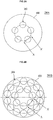
- FIGs. 2A and 2B are plan views of wafer carriers (or susceptors) 200A and 200B in accordance with the present invention.
- Pockets 300 arranged in one concentric circular line around the center of the wafer carrier 200A, as shown in FIG. 2A , or pockets 300 arranged in two concentric circular lines around the center of the wafer carrier 200B, as shown in FIG. 2B , may be formed on the surface of a carrier body 400 of the wafer carrier 200A or 200B.
- the arrangement shape of the pockets 300, the shape of each pocket 300 and the number of the pockets 300 on the wafer carriers 200A and 200B are not limited thereto.
- the pockets 300 may be arranged on the carrier body 400 in a shape other than one concentric circular line or two concentric circular lines. Further, 1 to 50 or more pockets 300 may be arranged on the wafer carrier 200A or 200B according to the size of a passive subject, i.e., wafer, on which deposition will be executed, mounted on each pocket 300 or the capacity of a reaction chamber. Still further, the pocket 300 may be formed in a circular shape or in a flat structure obtained by cutting one end of a circular shape.
- a shaft-coupling groove (not shown) is formed at the center of the lower surface of the wafer carrier 200A or 200B, and for example, the rotary shaft 150, as shown in FIG. 1 , may be coupled with the shaft-coupling groove.
- the wafer carrier 200A or 200B exemplarily shown in FIG. 2A or 2B may be disposed within the chamber 120 in the same manner as the wafer carrier 130 shown in FIG. 1 , this present invention is not limited thereto.
- the carrier body 400 has insertion spaces corresponding in number to the number of the pockets 300, and each insertion space has a structure to which the pocket 300 may be detachably attached.
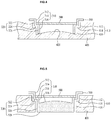
- FIG. 3 is a partial exploded view of a cross-section taken along the line A-A' of a pocket 300 and a carrier body 400 exemplarily shown in FIG. 2A or 2B in accordance with the present invention.
- the pocket 300 in accordance with this present invention includes a front support part 310 and a rear coupling part 320.
- the front support part 310 serves to support a wafer 500, and includes a first inner side surface 312, a first inner bottom surface 314, a second inner side surface 316 and a second inner bottom surface 318.
- the first inner side surface 312 is extended in a first direction in which the pocket 300 is inserted into the carrier body 400.
- the first inner bottom surface 314 is extended from the first inner side surface 312 in a second direction different from the first direction, and an edge 502 of the wafer 500 is placed on the first inner bottom surface 314.
- the edge 502 of the wafer 500 may be placed on the first inner bottom surface 314, and a separation distance d1 between a front end 504 of the wafer 500 and the first inner side surface 312 may be '0' or more.
- the first direction and the second direction may be perpendicular to each other.
- the second inner side surface 316 is extended from the first inner bottom surface 314 in a third direction.
- the third direction may be identical with the first direction, the disclosure is not limited thereto.
- the second inner bottom surface 318 is extended from the second inner side surface 316 in a fourth direction, and corresponds to the bottom of the pocket 300.
- fourth direction may be identical with the second direction, the disclosure is not limited thereto.
- the wafer carrier may further include a first fixing part (not shown) fixing the wafer 500 and the pocket 300, a second fixing part (not shown) fixing the pocket 300 and the carrier body 400, or a third fixing part (not shown) simultaneously fixing the wafer 500, the pocket 300 and the carrier body 400.
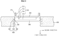
- FIGs. 4 to 9 and FIG. 11 are partial cross-sectional views taken along the line A-A' of pockets 300 and carrier bodies 400 exemplarily shown in FIG. 2A or 2B in accordance with the present invention.
- the second inner bottom surface 318 exemplarily shown in FIG. 3 may be omitted.
- the pocket 300 may be formed in a hole shape having no bottom, as exemplarily shown in FIG. 4 or 8 .
- first and second inner bottom surfaces 314 and 318 may have a convex shape or a concave shape toward the wafer 500.
- the second inner bottom surface 318 may have a convex shape toward the wafer 500, as exemplarily shown in FIG. 5 , or have a concave shape toward the wafer 500, as exemplarily shown in FIG. 6 .
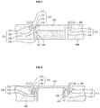
- At least one of the first and second inner bottom surfaces 314 and 318 may have at least one stepped portion.
- a groove 340 is formed at the edge of the second inner bottom surface 318, as exemplarily shown in FIG. 7
- a bottom surface 342 of the edge of the second inner bottom surface 318 has a stepped difference with the center of the second inner bottom surface 318.
- at least one of the first and second inner bottom surfaces 314 and 318 may have an inclined shape.
- the reason why the shape of at least one of the first and second inner bottom surfaces 314 and 318 is varied is to uniformize different temperatures of the edge and the center of the wafer 500, during the growth of the wafer 500, for example, when the wafer 500 is heated by the heating unit 160 exemplarily shown in FIG. 1 .
- the rear coupling part 320 of the pocket 300 is coupled with the carrier body 400 on the rear surface of the pocket 300.
- the rear coupling part 320 and the carrier body 400 have shapes corresponding to each other so as to be coupled with each other.
- the rear coupling part 320 includes a first outer side surface 322, a first outer bottom surface 324, a second outer side surface 326 and a second outer bottom surface 328.
- the first outer side surface 322 is extended in a fifth direction on the side of the pocket 300 opposite to the first inner side surface 312.
- the fifth direction may be identical with the first direction, the disclosure is not limited thereto.
- the first outer bottom surface 324 is extended from the first outer side surface 322 in a sixth direction different from the fifth direction on the side of the pocket 300 opposite to the first inner bottom surface 314.
- the sixth direction may be identical with the second direction, the disclosure is not limited thereto.
- the second outer side surface 326 is extended from the first outer bottom surface 324 in a seventh direction on the side of the pocket 300 opposite to the second inner side surface 316.
- the seventh direction may be identical with the first direction, the disclosure is not limited thereto.
- the second outer bottom surface 328 is extended from the second outer side surface 326 in an eighth direction on the side of the pocket 300 opposite to the second inner bottom surface 318.
- eighth direction may be identical with the second direction, the disclosure is not limited thereto.
- the second outer bottom surface 328 may also be omitted from the rear coupling part 320, as exemplarily shown in FIG. 4 or 8 .
- the carrier body 400 may include a third inner side surface 412, a third inner bottom surface 414, a fourth inner side surface 416, a fourth inner bottom surface 420 and a third outer bottom surface 440.
- the third inner side surface 412 faces the first outer side surface 322, and is extended in a ninth direction.
- the ninth direction may be the first direction, the disclosure is not limited thereto.
- the third inner bottom surface 414 faces the first outer bottom surface 324, and is extended from the third inner side surface 412 in a tenth direction.
- the tenth direction may be the second direction, the disclosure is not limited thereto.
- the fourth inner side surface 416 faces the second outer side surface 326, and is extended from the third inner bottom surface 414 in an eleventh direction.
- the eleventh direction may be the first direction, the disclosure is not limited thereto.
- a separation distance d2 between the third inner side surface 412 and the first outer side surface 322 may be '0' or more
- a separation distance d3 between the fourth inner side surface 416 and the second outer side surface 326 may be '0' or more.
- the fourth inner bottom surface 420 faces the second outer bottom surface 328, and is extended from the fourth inner side surface 416 in a twelfth direction.
- twelfth direction may be the second direction, the disclosure is not limited thereto.
- At least one of the third and fourth inner bottom surfaces 414 and 420 may have a flat shape, as exemplarily shown in FIG. 3 , have a convex shape or a concave shape, or have at least one stepped portion.
- the fourth inner bottom surface 420 may have a convex shape toward the wafer 500, as exemplarily shown in FIG. 4 .
- the fourth inner bottom surface 420 may have a concave shape toward the wafer 500.
- the third outer bottom surface 440 may be located at the side of the wafer body 400 opposite to the fourth inner bottom surface 420, and have at least one stepped portion.
- the third outer bottom surface 440 may have a stepped portion, as exemplarily shown in FIG. 6 .
- the space 402 into which the above-described pocket 300 is inserted may be formed in the shape of a groove formed on the upper surface of the carrier body 400.
- the carrier body 400 has the fourth inner bottom surface 420 and the third outer bottom surface 440, as exemplarily shown in FIG. 3 , 4 or 6 .
- the insertion space 402 may be formed in the shape of a hole passing through the carrier body 400.
- the fourth inner bottom surface 420 and the third outer bottom surface 440 are omitted from the carrier body 400, as exemplarily shown in FIG. 5 , 7 , 8 , 9 or 11 .
- the reason why the shape of at least one of the third inner bottom surface 414, the fourth inner bottom surface 420 and the third outer bottom surface 440 of the carrier body 400 is varied is to uniformize different temperatures of the edge and the center of the wafer 500, during the growth of the wafer 500, for example, when the wafer 500 is heated by the heating unit 160 exemplarily shown in FIG. 1 .
- a first height h1 of the second outer side surface 326 may be '0' or more. If the first height h1 is '0' or more, the wafer 500 is placed on the first and second inner bottom surfaces 314 and 318.
- first height h1 of the second outer side surface 326 may be equal to or smaller than a second height h2 of the fourth inner side surface 416.
- first height h1 becomes gradually smaller than the second height h2
- the temperature around the center of the pocket 300 rather than the edge of the pocket 300 is relatively lowered.
- the area of a region where the center of the pocket 300 and the carrier body 400 are opposite to each other is smaller than the area of a region where the edge of the pocket 300 and the carrier body 400 are opposite to each other and thus a smaller amount of heat from the carrier body 400 is transmitted to the center of the pocket 300 than the edge of the pocket 300.
- a third height h3 of the first outer side surface 322 and a fourth height h4 of the third inner side surface 412 may be equal or different.
- the insertion depths of the plural pockets 300 into the carrier body 400 may be equal or different. Namely, at least one of a difference ⁇ h1 between the first height h1 and the second height h2 and a difference ⁇ h2 between the third height h3 and the fourth height h4 may be uniform or varied according to the plural pockets 300.
- the reason why the first to fourth heights h1 to h4 are varied is to uniformize different temperatures of the edge and the center of the wafer 500, during the growth of the wafer 500, for example, when the wafer 500 is heated by the heating unit 160 exemplarily shown in FIG. 1 .
- a temperature difference between the edge and the center of the wafer 500 may be compensated for by adjusting a thickness t1 of the bottom of the pocket 300 and a thickness t2 of the bottom of the carrier body 400 exemplarily shown in FIG. 3 .
- the thickness t1 of the bottom of the pocket 300 is varied according to the edge and the center of the pocket 300, as exemplarily shown in FIG. 5 , 6 or 7 , the temperature of the edge of the wafer 500 and the temperature of the center of the wafer 500 may become uniform.
- the thickness t2 of the bottom of the carrier body 400 is varied according to the edge and the center of the carrier body 400, as exemplarily shown in FIG. 4 or 6 , the temperature of the edge of the wafer 500 and the temperature of the center of the wafer 500 may become uniform.
- the pocket 300 may be separated from the carrier body 400 by centrifugal force when the wafer carrier 200A or 200B is rotated after the above-described pocket 300 is coupled with the carrier body 400.
- the pocket 300 may further include a support projection
- the carrier body 400 may further include a support groove.
- a support projection 330 of the pocket 300 may be protruded from the first outer bottom surface 324 toward the third inner bottom surface 414 of the carrier body 400.
- a support groove 430 may be formed on the third inner bottom surface 414 so that the support projection 330 of the pocket 300 may be inserted into the support groove 430.
- a support projection (not shown) of the pocket 300 may be protruded from the first outer side surface 322 toward the third inner side surface 412 of the carrier body 400.
- a support groove (not shown) may be formed on the third inner side surface 412 so that the support projection (not shown) of the pocket 300 may be inserted into the support groove (not shown).
- the rear coupling part 320 and an inner side wall 410 of the carrier body 400 may be coupled with each other by bent shapes thereof.
- the disclosure is not limited thereto, and the pocket 300 may be detachably attached to the carrier body 400 in various shapes.
- the outer side wall of the circular pocket 300 may have a male screw thread shape
- the inner side wall of the carrier body 400 may have a female screw thread shape
- the rear coupling part 350 of the pocket 300 has an outer side wall 352 provided with a male screw thread formed thereon
- the carrier body 400 has an inner side wall 450 provided with a female screw thread formed thereon. Therefore, the outer side wall 352 of the rear coupling part 350 and the inner side wall 450 of the carrier body 400 may be coupled by connection between the male screw thread and the female screw thread.
- outer side wall 352 of the rear coupling part 350 and the inner side wall 450 of the carrier body 400 are not limited to the above-described screw thread shapes.
- the outer side wall 352 and the inner side wall 450 may have various shapes, such as a right-handed screw thread and a left-handed screw thread.
- FIG. 10 is a schematic plan view of the pocket 300 exemplarily shown in FIG. 9 .
- At least one scale mark 302 may be formed on an upper edge surface 311 of the pocket 300, and at least one indicator 402 may be formed on the upper edge of the carrier body 400 neighboring the upper edge surface 311 of the pocket 300. Therefore, when the male screw thread-shaped pocket 300 is rotated in the clockwise or counterclockwise direction and is inserted into the female screw thread-shaped carrier body 400, the rotating degree of the pocket 300, i.e., the insertion depth of the pocket 300 into the carrier body 400, may be estimated by observing the scale marks 302 based on the indicators 402. For this purpose, the number '0' may be expressed at one of the scale marks 302.
- the rear coupling part of the pocket 300 may have a coupling projection 360, and the carrier body 400 may have at least one coupling groove 460. Therefore, when at least one pocket 300 is pressed in the first direction, the at least one pocket 300 may be coupled with the carrier body 400 by fixing the coupling projection 360 to the at least one coupling groove 460.
- the coupling projection 360 of the pocket 300 is protruded in the second direction different from the first direction in which the pocket 300 is inserted into the carrier body 400.
- the at least one coupling groove 460 has a proper shape to fix the coupling projection 360 thereto, and is formed on the inner side wall of the carrier body 400.
- the at least one coupling groove 460 may be plural coupling grooves separated from each other by a designated interval.
- first to third coupling grooves 462, 464 and 466 are formed at a designated interval.
- scale marks 370 for measurement of a depth of the insertion of the pocket 300 into the carrier body 400 may be formed on the outer side wall of the rear coupling part of the pocket 300. Namely, which coupling groove among the first to third coupling grooves 462, 464 and 466 into which the coupling protrusion 360 is inserted may be estimated through the number of the exposed scale marks 370 when the coupling protrusion 360 is inserted into the first coupling groove 462 located at the uppermost end of the inner side wall of the carrier body 400, the number of the exposed scale marks 370 when the coupling protrusion 360 is inserted into the second coupling groove 464 located under the first coupling groove 462, and the number of the exposed scale marks 370 when the coupling protrusion 360 is inserted into the third coupling groove 466 located under the second coupling groove 464.
- a semiconductor manufacturing apparatus in accordance with the present invention may attach and detach pockets to and from a wafer carrier and, if a pocket is damaged, the damaged pocket alone may be replaced without replacement of the entirety of the wafer carrier including the damaged pocket, thereby shortening process time and reducing process expenses. Further, the semiconductor manufacturing apparatus allows the pockets to have different structures according to the positions of the pockets on the wafer carrier so that the uniform growth of a material may be achieved on the surfaces of wafers regardless of the positions of the pockets.
Landscapes
- Container, Conveyance, Adherence, Positioning, Of Wafer (AREA)
- Packaging Frangible Articles (AREA)
- Chemical Vapour Deposition (AREA)
Applications Claiming Priority (1)
| Application Number | Priority Date | Filing Date | Title |
|---|---|---|---|
| KR1020120015984A KR101928356B1 (ko) | 2012-02-16 | 2012-02-16 | 반도체 제조 장치 |
Publications (3)
| Publication Number | Publication Date |
|---|---|
| EP2629327A2 EP2629327A2 (en) | 2013-08-21 |
| EP2629327A3 EP2629327A3 (en) | 2017-04-05 |
| EP2629327B1 true EP2629327B1 (en) | 2020-04-01 |
Family
ID=47722104
Family Applications (1)
| Application Number | Title | Priority Date | Filing Date |
|---|---|---|---|
| EP13155303.4A Not-in-force EP2629327B1 (en) | 2012-02-16 | 2013-02-14 | Semiconductor manufacturing apparatus |
Country Status (5)
| Country | Link |
|---|---|
| US (1) | US9418885B2 (https=) |
| EP (1) | EP2629327B1 (https=) |
| JP (1) | JP6126405B2 (https=) |
| KR (1) | KR101928356B1 (https=) |
| CN (1) | CN103255393B (https=) |
Families Citing this family (313)
| Publication number | Priority date | Publication date | Assignee | Title |
|---|---|---|---|---|
| US9394608B2 (en) | 2009-04-06 | 2016-07-19 | Asm America, Inc. | Semiconductor processing reactor and components thereof |
| US20130023129A1 (en) | 2011-07-20 | 2013-01-24 | Asm America, Inc. | Pressure transmitter for a semiconductor processing environment |
| US10714315B2 (en) | 2012-10-12 | 2020-07-14 | Asm Ip Holdings B.V. | Semiconductor reaction chamber showerhead |
| US20160376700A1 (en) | 2013-02-01 | 2016-12-29 | Asm Ip Holding B.V. | System for treatment of deposition reactor |
| ITCO20130041A1 (it) * | 2013-09-27 | 2015-03-28 | Lpe Spa | Suscettore con elemento di supporto |
| ITCO20130073A1 (it) * | 2013-12-19 | 2015-06-20 | Lpe Spa | Camera di reazione di un reattore per crescite epitassiali adatta per l'uso con un dispositivo di carico/scarico e reattore |
| KR102181390B1 (ko) * | 2014-02-07 | 2020-11-20 | 엘지이노텍 주식회사 | 반도체 제조 장치 |
| US11015245B2 (en) | 2014-03-19 | 2021-05-25 | Asm Ip Holding B.V. | Gas-phase reactor and system having exhaust plenum and components thereof |
| WO2016001863A1 (en) | 2014-07-03 | 2016-01-07 | Lpe S.P.A. | Tool for manipulating substrates, manipulation method and epitaxial reactor |
| US10858737B2 (en) | 2014-07-28 | 2020-12-08 | Asm Ip Holding B.V. | Showerhead assembly and components thereof |
| US10941490B2 (en) | 2014-10-07 | 2021-03-09 | Asm Ip Holding B.V. | Multiple temperature range susceptor, assembly, reactor and system including the susceptor, and methods of using the same |
| KR101682776B1 (ko) * | 2014-12-31 | 2016-12-05 | 주식회사 티씨케이 | 포켓 교체형 서셉터 |
| US10276355B2 (en) | 2015-03-12 | 2019-04-30 | Asm Ip Holding B.V. | Multi-zone reactor, system including the reactor, and method of using the same |
| US10458018B2 (en) | 2015-06-26 | 2019-10-29 | Asm Ip Holding B.V. | Structures including metal carbide material, devices including the structures, and methods of forming same |
| US10211308B2 (en) | 2015-10-21 | 2019-02-19 | Asm Ip Holding B.V. | NbMC layers |
| US11139308B2 (en) | 2015-12-29 | 2021-10-05 | Asm Ip Holding B.V. | Atomic layer deposition of III-V compounds to form V-NAND devices |
| US10529554B2 (en) | 2016-02-19 | 2020-01-07 | Asm Ip Holding B.V. | Method for forming silicon nitride film selectively on sidewalls or flat surfaces of trenches |
| US10343920B2 (en) | 2016-03-18 | 2019-07-09 | Asm Ip Holding B.V. | Aligned carbon nanotubes |
| US10190213B2 (en) | 2016-04-21 | 2019-01-29 | Asm Ip Holding B.V. | Deposition of metal borides |
| US10367080B2 (en) | 2016-05-02 | 2019-07-30 | Asm Ip Holding B.V. | Method of forming a germanium oxynitride film |
| US11453943B2 (en) | 2016-05-25 | 2022-09-27 | Asm Ip Holding B.V. | Method for forming carbon-containing silicon/metal oxide or nitride film by ALD using silicon precursor and hydrocarbon precursor |
| US9859151B1 (en) | 2016-07-08 | 2018-01-02 | Asm Ip Holding B.V. | Selective film deposition method to form air gaps |
| US10612137B2 (en) | 2016-07-08 | 2020-04-07 | Asm Ip Holdings B.V. | Organic reactants for atomic layer deposition |
| US9887082B1 (en) | 2016-07-28 | 2018-02-06 | Asm Ip Holding B.V. | Method and apparatus for filling a gap |
| KR102532607B1 (ko) | 2016-07-28 | 2023-05-15 | 에이에스엠 아이피 홀딩 비.브이. | 기판 가공 장치 및 그 동작 방법 |
| US9812320B1 (en) | 2016-07-28 | 2017-11-07 | Asm Ip Holding B.V. | Method and apparatus for filling a gap |
| US10643826B2 (en) | 2016-10-26 | 2020-05-05 | Asm Ip Holdings B.V. | Methods for thermally calibrating reaction chambers |
| US11532757B2 (en) | 2016-10-27 | 2022-12-20 | Asm Ip Holding B.V. | Deposition of charge trapping layers |
| US10714350B2 (en) | 2016-11-01 | 2020-07-14 | ASM IP Holdings, B.V. | Methods for forming a transition metal niobium nitride film on a substrate by atomic layer deposition and related semiconductor device structures |
| KR102546317B1 (ko) | 2016-11-15 | 2023-06-21 | 에이에스엠 아이피 홀딩 비.브이. | 기체 공급 유닛 및 이를 포함하는 기판 처리 장치 |
| KR102762543B1 (ko) | 2016-12-14 | 2025-02-05 | 에이에스엠 아이피 홀딩 비.브이. | 기판 처리 장치 |
| US11581186B2 (en) | 2016-12-15 | 2023-02-14 | Asm Ip Holding B.V. | Sequential infiltration synthesis apparatus |
| US11447861B2 (en) | 2016-12-15 | 2022-09-20 | Asm Ip Holding B.V. | Sequential infiltration synthesis apparatus and a method of forming a patterned structure |
| KR102700194B1 (ko) | 2016-12-19 | 2024-08-28 | 에이에스엠 아이피 홀딩 비.브이. | 기판 처리 장치 |
| US10269558B2 (en) | 2016-12-22 | 2019-04-23 | Asm Ip Holding B.V. | Method of forming a structure on a substrate |
| US10867788B2 (en) | 2016-12-28 | 2020-12-15 | Asm Ip Holding B.V. | Method of forming a structure on a substrate |
| US11390950B2 (en) | 2017-01-10 | 2022-07-19 | Asm Ip Holding B.V. | Reactor system and method to reduce residue buildup during a film deposition process |
| US10468261B2 (en) | 2017-02-15 | 2019-11-05 | Asm Ip Holding B.V. | Methods for forming a metallic film on a substrate by cyclical deposition and related semiconductor device structures |
| US10529563B2 (en) | 2017-03-29 | 2020-01-07 | Asm Ip Holdings B.V. | Method for forming doped metal oxide films on a substrate by cyclical deposition and related semiconductor device structures |
| KR102457289B1 (ko) | 2017-04-25 | 2022-10-21 | 에이에스엠 아이피 홀딩 비.브이. | 박막 증착 방법 및 반도체 장치의 제조 방법 |
| US10892156B2 (en) | 2017-05-08 | 2021-01-12 | Asm Ip Holding B.V. | Methods for forming a silicon nitride film on a substrate and related semiconductor device structures |
| US10770286B2 (en) | 2017-05-08 | 2020-09-08 | Asm Ip Holdings B.V. | Methods for selectively forming a silicon nitride film on a substrate and related semiconductor device structures |
| KR102417931B1 (ko) * | 2017-05-30 | 2022-07-06 | 에이에스엠 아이피 홀딩 비.브이. | 기판 지지 장치 및 이를 포함하는 기판 처리 장치 |
| US10886123B2 (en) | 2017-06-02 | 2021-01-05 | Asm Ip Holding B.V. | Methods for forming low temperature semiconductor layers and related semiconductor device structures |
| US12040200B2 (en) | 2017-06-20 | 2024-07-16 | Asm Ip Holding B.V. | Semiconductor processing apparatus and methods for calibrating a semiconductor processing apparatus |
| US11306395B2 (en) | 2017-06-28 | 2022-04-19 | Asm Ip Holding B.V. | Methods for depositing a transition metal nitride film on a substrate by atomic layer deposition and related deposition apparatus |
| KR20190009245A (ko) | 2017-07-18 | 2019-01-28 | 에이에스엠 아이피 홀딩 비.브이. | 반도체 소자 구조물 형성 방법 및 관련된 반도체 소자 구조물 |
| US11374112B2 (en) | 2017-07-19 | 2022-06-28 | Asm Ip Holding B.V. | Method for depositing a group IV semiconductor and related semiconductor device structures |
| US11018002B2 (en) | 2017-07-19 | 2021-05-25 | Asm Ip Holding B.V. | Method for selectively depositing a Group IV semiconductor and related semiconductor device structures |
| US10541333B2 (en) | 2017-07-19 | 2020-01-21 | Asm Ip Holding B.V. | Method for depositing a group IV semiconductor and related semiconductor device structures |
| US10590535B2 (en) | 2017-07-26 | 2020-03-17 | Asm Ip Holdings B.V. | Chemical treatment, deposition and/or infiltration apparatus and method for using the same |
| TWI815813B (zh) | 2017-08-04 | 2023-09-21 | 荷蘭商Asm智慧財產控股公司 | 用於分配反應腔內氣體的噴頭總成 |
| US10770336B2 (en) | 2017-08-08 | 2020-09-08 | Asm Ip Holding B.V. | Substrate lift mechanism and reactor including same |
| US10692741B2 (en) | 2017-08-08 | 2020-06-23 | Asm Ip Holdings B.V. | Radiation shield |
| US11769682B2 (en) | 2017-08-09 | 2023-09-26 | Asm Ip Holding B.V. | Storage apparatus for storing cassettes for substrates and processing apparatus equipped therewith |
| US11139191B2 (en) | 2017-08-09 | 2021-10-05 | Asm Ip Holding B.V. | Storage apparatus for storing cassettes for substrates and processing apparatus equipped therewith |
| CN109411401B (zh) * | 2017-08-18 | 2020-12-25 | 上海新昇半导体科技有限公司 | 衬底支撑装置以及外延生长设备 |
| US11830730B2 (en) | 2017-08-29 | 2023-11-28 | Asm Ip Holding B.V. | Layer forming method and apparatus |
| US11056344B2 (en) | 2017-08-30 | 2021-07-06 | Asm Ip Holding B.V. | Layer forming method |
| KR102540125B1 (ko) * | 2017-08-30 | 2023-06-05 | 주성엔지니어링(주) | 기판안치수단 및 기판처리장치 |
| WO2019045340A1 (ko) * | 2017-08-30 | 2019-03-07 | 주성엔지니어링(주) | 기판안치수단 및 기판처리장치 |
| US11295980B2 (en) | 2017-08-30 | 2022-04-05 | Asm Ip Holding B.V. | Methods for depositing a molybdenum metal film over a dielectric surface of a substrate by a cyclical deposition process and related semiconductor device structures |
| KR102491945B1 (ko) | 2017-08-30 | 2023-01-26 | 에이에스엠 아이피 홀딩 비.브이. | 기판 처리 장치 |
| KR102401446B1 (ko) | 2017-08-31 | 2022-05-24 | 에이에스엠 아이피 홀딩 비.브이. | 기판 처리 장치 |
| KR102630301B1 (ko) | 2017-09-21 | 2024-01-29 | 에이에스엠 아이피 홀딩 비.브이. | 침투성 재료의 순차 침투 합성 방법 처리 및 이를 이용하여 형성된 구조물 및 장치 |
| US10844484B2 (en) | 2017-09-22 | 2020-11-24 | Asm Ip Holding B.V. | Apparatus for dispensing a vapor phase reactant to a reaction chamber and related methods |
| US10658205B2 (en) | 2017-09-28 | 2020-05-19 | Asm Ip Holdings B.V. | Chemical dispensing apparatus and methods for dispensing a chemical to a reaction chamber |
| US10403504B2 (en) | 2017-10-05 | 2019-09-03 | Asm Ip Holding B.V. | Method for selectively depositing a metallic film on a substrate |
| US10923344B2 (en) | 2017-10-30 | 2021-02-16 | Asm Ip Holding B.V. | Methods for forming a semiconductor structure and related semiconductor structures |
| US10910262B2 (en) | 2017-11-16 | 2021-02-02 | Asm Ip Holding B.V. | Method of selectively depositing a capping layer structure on a semiconductor device structure |
| US11022879B2 (en) | 2017-11-24 | 2021-06-01 | Asm Ip Holding B.V. | Method of forming an enhanced unexposed photoresist layer |
| TWI791689B (zh) | 2017-11-27 | 2023-02-11 | 荷蘭商Asm智慧財產控股私人有限公司 | 包括潔淨迷你環境之裝置 |
| JP7214724B2 (ja) | 2017-11-27 | 2023-01-30 | エーエスエム アイピー ホールディング ビー.ブイ. | バッチ炉で利用されるウェハカセットを収納するための収納装置 |
| US10872771B2 (en) | 2018-01-16 | 2020-12-22 | Asm Ip Holding B. V. | Method for depositing a material film on a substrate within a reaction chamber by a cyclical deposition process and related device structures |
| KR102695659B1 (ko) | 2018-01-19 | 2024-08-14 | 에이에스엠 아이피 홀딩 비.브이. | 플라즈마 보조 증착에 의해 갭 충진 층을 증착하는 방법 |
| TWI799494B (zh) | 2018-01-19 | 2023-04-21 | 荷蘭商Asm 智慧財產控股公司 | 沈積方法 |
| US11018047B2 (en) | 2018-01-25 | 2021-05-25 | Asm Ip Holding B.V. | Hybrid lift pin |
| USD880437S1 (en) | 2018-02-01 | 2020-04-07 | Asm Ip Holding B.V. | Gas supply plate for semiconductor manufacturing apparatus |
| US11081345B2 (en) | 2018-02-06 | 2021-08-03 | Asm Ip Holding B.V. | Method of post-deposition treatment for silicon oxide film |
| US11685991B2 (en) | 2018-02-14 | 2023-06-27 | Asm Ip Holding B.V. | Method for depositing a ruthenium-containing film on a substrate by a cyclical deposition process |
| US10896820B2 (en) | 2018-02-14 | 2021-01-19 | Asm Ip Holding B.V. | Method for depositing a ruthenium-containing film on a substrate by a cyclical deposition process |
| US10731249B2 (en) | 2018-02-15 | 2020-08-04 | Asm Ip Holding B.V. | Method of forming a transition metal containing film on a substrate by a cyclical deposition process, a method for supplying a transition metal halide compound to a reaction chamber, and related vapor deposition apparatus |
| KR102636427B1 (ko) | 2018-02-20 | 2024-02-13 | 에이에스엠 아이피 홀딩 비.브이. | 기판 처리 방법 및 장치 |
| US10975470B2 (en) | 2018-02-23 | 2021-04-13 | Asm Ip Holding B.V. | Apparatus for detecting or monitoring for a chemical precursor in a high temperature environment |
| US11473195B2 (en) | 2018-03-01 | 2022-10-18 | Asm Ip Holding B.V. | Semiconductor processing apparatus and a method for processing a substrate |
| US11629406B2 (en) | 2018-03-09 | 2023-04-18 | Asm Ip Holding B.V. | Semiconductor processing apparatus comprising one or more pyrometers for measuring a temperature of a substrate during transfer of the substrate |
| US11114283B2 (en) | 2018-03-16 | 2021-09-07 | Asm Ip Holding B.V. | Reactor, system including the reactor, and methods of manufacturing and using same |
| KR102646467B1 (ko) | 2018-03-27 | 2024-03-11 | 에이에스엠 아이피 홀딩 비.브이. | 기판 상에 전극을 형성하는 방법 및 전극을 포함하는 반도체 소자 구조 |
| US11088002B2 (en) | 2018-03-29 | 2021-08-10 | Asm Ip Holding B.V. | Substrate rack and a substrate processing system and method |
| US11230766B2 (en) | 2018-03-29 | 2022-01-25 | Asm Ip Holding B.V. | Substrate processing apparatus and method |
| KR102501472B1 (ko) | 2018-03-30 | 2023-02-20 | 에이에스엠 아이피 홀딩 비.브이. | 기판 처리 방법 |
| KR102600229B1 (ko) | 2018-04-09 | 2023-11-10 | 에이에스엠 아이피 홀딩 비.브이. | 기판 지지 장치, 이를 포함하는 기판 처리 장치 및 기판 처리 방법 |
| US12025484B2 (en) | 2018-05-08 | 2024-07-02 | Asm Ip Holding B.V. | Thin film forming method |
| TWI843623B (zh) | 2018-05-08 | 2024-05-21 | 荷蘭商Asm Ip私人控股有限公司 | 藉由循環沉積製程於基板上沉積氧化物膜之方法及相關裝置結構 |
| US12272527B2 (en) | 2018-05-09 | 2025-04-08 | Asm Ip Holding B.V. | Apparatus for use with hydrogen radicals and method of using same |
| TWI794475B (zh) * | 2018-05-09 | 2023-03-01 | 德商索萊爾有限公司 | 用於接收多個基板以進行處理之保持裝置、處理系統及方法 |
| KR20190129718A (ko) | 2018-05-11 | 2019-11-20 | 에이에스엠 아이피 홀딩 비.브이. | 기판 상에 피도핑 금속 탄화물 막을 형성하는 방법 및 관련 반도체 소자 구조 |
| KR102596988B1 (ko) | 2018-05-28 | 2023-10-31 | 에이에스엠 아이피 홀딩 비.브이. | 기판 처리 방법 및 그에 의해 제조된 장치 |
| US11718913B2 (en) | 2018-06-04 | 2023-08-08 | Asm Ip Holding B.V. | Gas distribution system and reactor system including same |
| TWI840362B (zh) | 2018-06-04 | 2024-05-01 | 荷蘭商Asm Ip私人控股有限公司 | 水氣降低的晶圓處置腔室 |
| US11286562B2 (en) | 2018-06-08 | 2022-03-29 | Asm Ip Holding B.V. | Gas-phase chemical reactor and method of using same |
| US10797133B2 (en) | 2018-06-21 | 2020-10-06 | Asm Ip Holding B.V. | Method for depositing a phosphorus doped silicon arsenide film and related semiconductor device structures |
| KR102568797B1 (ko) | 2018-06-21 | 2023-08-21 | 에이에스엠 아이피 홀딩 비.브이. | 기판 처리 시스템 |
| US11499222B2 (en) | 2018-06-27 | 2022-11-15 | Asm Ip Holding B.V. | Cyclic deposition methods for forming metal-containing material and films and structures including the metal-containing material |
| TWI871083B (zh) | 2018-06-27 | 2025-01-21 | 荷蘭商Asm Ip私人控股有限公司 | 用於形成含金屬材料之循環沉積製程 |
| KR102686758B1 (ko) | 2018-06-29 | 2024-07-18 | 에이에스엠 아이피 홀딩 비.브이. | 박막 증착 방법 및 반도체 장치의 제조 방법 |
| US10612136B2 (en) | 2018-06-29 | 2020-04-07 | ASM IP Holding, B.V. | Temperature-controlled flange and reactor system including same |
| US10388513B1 (en) | 2018-07-03 | 2019-08-20 | Asm Ip Holding B.V. | Method for depositing silicon-free carbon-containing film as gap-fill layer by pulse plasma-assisted deposition |
| US10755922B2 (en) | 2018-07-03 | 2020-08-25 | Asm Ip Holding B.V. | Method for depositing silicon-free carbon-containing film as gap-fill layer by pulse plasma-assisted deposition |
| US11053591B2 (en) | 2018-08-06 | 2021-07-06 | Asm Ip Holding B.V. | Multi-port gas injection system and reactor system including same |
| US10883175B2 (en) | 2018-08-09 | 2021-01-05 | Asm Ip Holding B.V. | Vertical furnace for processing substrates and a liner for use therein |
| US11430674B2 (en) | 2018-08-22 | 2022-08-30 | Asm Ip Holding B.V. | Sensor array, apparatus for dispensing a vapor phase reactant to a reaction chamber and related methods |
| US11024523B2 (en) | 2018-09-11 | 2021-06-01 | Asm Ip Holding B.V. | Substrate processing apparatus and method |
| KR102707956B1 (ko) | 2018-09-11 | 2024-09-19 | 에이에스엠 아이피 홀딩 비.브이. | 박막 증착 방법 |
| US11049751B2 (en) | 2018-09-14 | 2021-06-29 | Asm Ip Holding B.V. | Cassette supply system to store and handle cassettes and processing apparatus equipped therewith |
| CN110970344B (zh) | 2018-10-01 | 2024-10-25 | Asmip控股有限公司 | 衬底保持设备、包含所述设备的系统及其使用方法 |
| US11232963B2 (en) | 2018-10-03 | 2022-01-25 | Asm Ip Holding B.V. | Substrate processing apparatus and method |
| KR102592699B1 (ko) | 2018-10-08 | 2023-10-23 | 에이에스엠 아이피 홀딩 비.브이. | 기판 지지 유닛 및 이를 포함하는 박막 증착 장치와 기판 처리 장치 |
| KR102605121B1 (ko) | 2018-10-19 | 2023-11-23 | 에이에스엠 아이피 홀딩 비.브이. | 기판 처리 장치 및 기판 처리 방법 |
| KR102546322B1 (ko) | 2018-10-19 | 2023-06-21 | 에이에스엠 아이피 홀딩 비.브이. | 기판 처리 장치 및 기판 처리 방법 |
| USD948463S1 (en) | 2018-10-24 | 2022-04-12 | Asm Ip Holding B.V. | Susceptor for semiconductor substrate supporting apparatus |
| US12378665B2 (en) | 2018-10-26 | 2025-08-05 | Asm Ip Holding B.V. | High temperature coatings for a preclean and etch apparatus and related methods |
| US11087997B2 (en) | 2018-10-31 | 2021-08-10 | Asm Ip Holding B.V. | Substrate processing apparatus for processing substrates |
| KR102748291B1 (ko) | 2018-11-02 | 2024-12-31 | 에이에스엠 아이피 홀딩 비.브이. | 기판 지지 유닛 및 이를 포함하는 기판 처리 장치 |
| US11572620B2 (en) | 2018-11-06 | 2023-02-07 | Asm Ip Holding B.V. | Methods for selectively depositing an amorphous silicon film on a substrate |
| US11031242B2 (en) | 2018-11-07 | 2021-06-08 | Asm Ip Holding B.V. | Methods for depositing a boron doped silicon germanium film |
| US10818758B2 (en) | 2018-11-16 | 2020-10-27 | Asm Ip Holding B.V. | Methods for forming a metal silicate film on a substrate in a reaction chamber and related semiconductor device structures |
| US10847366B2 (en) | 2018-11-16 | 2020-11-24 | Asm Ip Holding B.V. | Methods for depositing a transition metal chalcogenide film on a substrate by a cyclical deposition process |
| US12040199B2 (en) | 2018-11-28 | 2024-07-16 | Asm Ip Holding B.V. | Substrate processing apparatus for processing substrates |
| US11217444B2 (en) | 2018-11-30 | 2022-01-04 | Asm Ip Holding B.V. | Method for forming an ultraviolet radiation responsive metal oxide-containing film |
| KR102636428B1 (ko) | 2018-12-04 | 2024-02-13 | 에이에스엠 아이피 홀딩 비.브이. | 기판 처리 장치를 세정하는 방법 |
| US11158513B2 (en) | 2018-12-13 | 2021-10-26 | Asm Ip Holding B.V. | Methods for forming a rhenium-containing film on a substrate by a cyclical deposition process and related semiconductor device structures |
| JP7504584B2 (ja) | 2018-12-14 | 2024-06-24 | エーエスエム・アイピー・ホールディング・ベー・フェー | 窒化ガリウムの選択的堆積を用いてデバイス構造体を形成する方法及びそのためのシステム |
| TWI866480B (zh) | 2019-01-17 | 2024-12-11 | 荷蘭商Asm Ip 私人控股有限公司 | 藉由循環沈積製程於基板上形成含過渡金屬膜之方法 |
| KR102727227B1 (ko) | 2019-01-22 | 2024-11-07 | 에이에스엠 아이피 홀딩 비.브이. | 기판 처리 장치 |
| CN111524788B (zh) | 2019-02-01 | 2023-11-24 | Asm Ip私人控股有限公司 | 氧化硅的拓扑选择性膜形成的方法 |
| TWI873122B (zh) | 2019-02-20 | 2025-02-21 | 荷蘭商Asm Ip私人控股有限公司 | 填充一基板之一表面內所形成的一凹槽的方法、根據其所形成之半導體結構、及半導體處理設備 |
| KR20200102357A (ko) | 2019-02-20 | 2020-08-31 | 에이에스엠 아이피 홀딩 비.브이. | 3-d nand 응용의 플러그 충진체 증착용 장치 및 방법 |
| KR102626263B1 (ko) | 2019-02-20 | 2024-01-16 | 에이에스엠 아이피 홀딩 비.브이. | 처리 단계를 포함하는 주기적 증착 방법 및 이를 위한 장치 |
| TWI845607B (zh) | 2019-02-20 | 2024-06-21 | 荷蘭商Asm Ip私人控股有限公司 | 用來填充形成於基材表面內之凹部的循環沉積方法及設備 |
| TWI842826B (zh) | 2019-02-22 | 2024-05-21 | 荷蘭商Asm Ip私人控股有限公司 | 基材處理設備及處理基材之方法 |
| KR102858005B1 (ko) | 2019-03-08 | 2025-09-09 | 에이에스엠 아이피 홀딩 비.브이. | 실리콘 질화물 층을 선택적으로 증착하는 방법, 및 선택적으로 증착된 실리콘 질화물 층을 포함하는 구조체 |
| KR102762833B1 (ko) | 2019-03-08 | 2025-02-04 | 에이에스엠 아이피 홀딩 비.브이. | SiOCN 층을 포함한 구조체 및 이의 형성 방법 |
| KR102782593B1 (ko) | 2019-03-08 | 2025-03-14 | 에이에스엠 아이피 홀딩 비.브이. | SiOC 층을 포함한 구조체 및 이의 형성 방법 |
| JP2020167398A (ja) | 2019-03-28 | 2020-10-08 | エーエスエム・アイピー・ホールディング・ベー・フェー | ドアオープナーおよびドアオープナーが提供される基材処理装置 |
| KR102809999B1 (ko) | 2019-04-01 | 2025-05-19 | 에이에스엠 아이피 홀딩 비.브이. | 반도체 소자를 제조하는 방법 |
| KR102897355B1 (ko) | 2019-04-19 | 2025-12-08 | 에이에스엠 아이피 홀딩 비.브이. | 층 형성 방법 및 장치 |
| KR20200125453A (ko) | 2019-04-24 | 2020-11-04 | 에이에스엠 아이피 홀딩 비.브이. | 기상 반응기 시스템 및 이를 사용하는 방법 |
| KR102929471B1 (ko) | 2019-05-07 | 2026-02-20 | 에이에스엠 아이피 홀딩 비.브이. | 딥 튜브가 있는 화학물질 공급원 용기 |
| KR102869364B1 (ko) | 2019-05-07 | 2025-10-10 | 에이에스엠 아이피 홀딩 비.브이. | 비정질 탄소 중합체 막을 개질하는 방법 |
| KR102929472B1 (ko) | 2019-05-10 | 2026-02-20 | 에이에스엠 아이피 홀딩 비.브이. | 표면 상에 재료를 증착하는 방법 및 본 방법에 따라 형성된 구조 |
| JP7612342B2 (ja) | 2019-05-16 | 2025-01-14 | エーエスエム・アイピー・ホールディング・ベー・フェー | ウェハボートハンドリング装置、縦型バッチ炉および方法 |
| JP7598201B2 (ja) | 2019-05-16 | 2024-12-11 | エーエスエム・アイピー・ホールディング・ベー・フェー | ウェハボートハンドリング装置、縦型バッチ炉および方法 |
| USD975665S1 (en) | 2019-05-17 | 2023-01-17 | Asm Ip Holding B.V. | Susceptor shaft |
| USD947913S1 (en) | 2019-05-17 | 2022-04-05 | Asm Ip Holding B.V. | Susceptor shaft |
| KR102901529B1 (ko) * | 2019-05-20 | 2025-12-18 | 주성엔지니어링(주) | 기판처리장치 |
| USD935572S1 (en) | 2019-05-24 | 2021-11-09 | Asm Ip Holding B.V. | Gas channel plate |
| USD922229S1 (en) | 2019-06-05 | 2021-06-15 | Asm Ip Holding B.V. | Device for controlling a temperature of a gas supply unit |
| KR20200141002A (ko) | 2019-06-06 | 2020-12-17 | 에이에스엠 아이피 홀딩 비.브이. | 배기 가스 분석을 포함한 기상 반응기 시스템을 사용하는 방법 |
| KR102918757B1 (ko) | 2019-06-10 | 2026-01-28 | 에이에스엠 아이피 홀딩 비.브이. | 석영 에피택셜 챔버를 세정하는 방법 |
| KR20200143254A (ko) | 2019-06-11 | 2020-12-23 | 에이에스엠 아이피 홀딩 비.브이. | 개질 가스를 사용하여 전자 구조를 형성하는 방법, 상기 방법을 수행하기 위한 시스템, 및 상기 방법을 사용하여 형성되는 구조 |
| USD944946S1 (en) | 2019-06-14 | 2022-03-01 | Asm Ip Holding B.V. | Shower plate |
| USD931978S1 (en) | 2019-06-27 | 2021-09-28 | Asm Ip Holding B.V. | Showerhead vacuum transport |
| KR102911421B1 (ko) | 2019-07-03 | 2026-01-12 | 에이에스엠 아이피 홀딩 비.브이. | 기판 처리 장치용 온도 제어 조립체 및 이를 사용하는 방법 |
| JP7499079B2 (ja) | 2019-07-09 | 2024-06-13 | エーエスエム・アイピー・ホールディング・ベー・フェー | 同軸導波管を用いたプラズマ装置、基板処理方法 |
| CN112216646B (zh) | 2019-07-10 | 2026-02-10 | Asmip私人控股有限公司 | 基板支撑组件及包括其的基板处理装置 |
| KR102895115B1 (ko) | 2019-07-16 | 2025-12-03 | 에이에스엠 아이피 홀딩 비.브이. | 기판 처리 장치 |
| KR102860110B1 (ko) | 2019-07-17 | 2025-09-16 | 에이에스엠 아이피 홀딩 비.브이. | 실리콘 게르마늄 구조를 형성하는 방법 |
| TWI826704B (zh) | 2019-07-17 | 2023-12-21 | 荷蘭商Asm Ip私人控股有限公司 | 自由基輔助引燃電漿系統和方法 |
| US11643724B2 (en) | 2019-07-18 | 2023-05-09 | Asm Ip Holding B.V. | Method of forming structures using a neutral beam |
| TWI839544B (zh) | 2019-07-19 | 2024-04-21 | 荷蘭商Asm Ip私人控股有限公司 | 形成形貌受控的非晶碳聚合物膜之方法 |
| KR102903090B1 (ko) | 2019-07-19 | 2025-12-19 | 에이에스엠 아이피 홀딩 비.브이. | 토폴로지-제어된 비정질 탄소 중합체 막을 형성하는 방법 |
| CN112309843B (zh) | 2019-07-29 | 2026-01-23 | Asmip私人控股有限公司 | 实现高掺杂剂掺入的选择性沉积方法 |
| CN112309900B (zh) | 2019-07-30 | 2025-11-04 | Asmip私人控股有限公司 | 基板处理设备 |
| KR20210015655A (ko) | 2019-07-30 | 2021-02-10 | 에이에스엠 아이피 홀딩 비.브이. | 기판 처리 장치 및 방법 |
| CN112309899B (zh) | 2019-07-30 | 2025-11-14 | Asmip私人控股有限公司 | 基板处理设备 |
| US11587814B2 (en) | 2019-07-31 | 2023-02-21 | Asm Ip Holding B.V. | Vertical batch furnace assembly |
| US11227782B2 (en) | 2019-07-31 | 2022-01-18 | Asm Ip Holding B.V. | Vertical batch furnace assembly |
| US11587815B2 (en) | 2019-07-31 | 2023-02-21 | Asm Ip Holding B.V. | Vertical batch furnace assembly |
| KR20210018759A (ko) | 2019-08-05 | 2021-02-18 | 에이에스엠 아이피 홀딩 비.브이. | 화학물질 공급원 용기를 위한 액체 레벨 센서 |
| KR20210018761A (ko) | 2019-08-09 | 2021-02-18 | 에이에스엠 아이피 홀딩 비.브이. | 냉각 장치를 포함한 히터 어셈블리 및 이를 사용하는 방법 |
| KR20210021266A (ko) | 2019-08-14 | 2021-02-25 | 에이에스엠 아이피 홀딩 비.브이. | 웨이퍼를 처리하는 장치 및 방법 |
| USD965524S1 (en) | 2019-08-19 | 2022-10-04 | Asm Ip Holding B.V. | Susceptor support |
| USD965044S1 (en) | 2019-08-19 | 2022-09-27 | Asm Ip Holding B.V. | Susceptor shaft |
| JP7810514B2 (ja) | 2019-08-21 | 2026-02-03 | エーエスエム・アイピー・ホールディング・ベー・フェー | 成膜原料混合ガス生成装置及び成膜装置 |
| USD979506S1 (en) | 2019-08-22 | 2023-02-28 | Asm Ip Holding B.V. | Insulator |
| KR20210024423A (ko) | 2019-08-22 | 2021-03-05 | 에이에스엠 아이피 홀딩 비.브이. | 홀을 구비한 구조체를 형성하기 위한 방법 |
| USD930782S1 (en) | 2019-08-22 | 2021-09-14 | Asm Ip Holding B.V. | Gas distributor |
| USD940837S1 (en) | 2019-08-22 | 2022-01-11 | Asm Ip Holding B.V. | Electrode |
| USD949319S1 (en) | 2019-08-22 | 2022-04-19 | Asm Ip Holding B.V. | Exhaust duct |
| US11286558B2 (en) | 2019-08-23 | 2022-03-29 | Asm Ip Holding B.V. | Methods for depositing a molybdenum nitride film on a surface of a substrate by a cyclical deposition process and related semiconductor device structures including a molybdenum nitride film |
| KR102928101B1 (ko) | 2019-08-23 | 2026-02-13 | 에이에스엠 아이피 홀딩 비.브이. | 비스(디에틸아미노)실란을 사용하여 peald에 의해 개선된 품질을 갖는 실리콘 산화물 막을 증착하기 위한 방법 |
| KR102868968B1 (ko) | 2019-09-03 | 2025-10-10 | 에이에스엠 아이피 홀딩 비.브이. | 칼코지나이드 막 및 상기 막을 포함한 구조체를 증착하기 위한 방법 및 장치 |
| KR102806450B1 (ko) | 2019-09-04 | 2025-05-12 | 에이에스엠 아이피 홀딩 비.브이. | 희생 캡핑 층을 이용한 선택적 증착 방법 |
| KR102733104B1 (ko) | 2019-09-05 | 2024-11-22 | 에이에스엠 아이피 홀딩 비.브이. | 기판 처리 장치 |
| US12469693B2 (en) | 2019-09-17 | 2025-11-11 | Asm Ip Holding B.V. | Method of forming a carbon-containing layer and structure including the layer |
| US11562901B2 (en) | 2019-09-25 | 2023-01-24 | Asm Ip Holding B.V. | Substrate processing method |
| CN112593212B (zh) | 2019-10-02 | 2023-12-22 | Asm Ip私人控股有限公司 | 通过循环等离子体增强沉积工艺形成拓扑选择性氧化硅膜的方法 |
| KR102948143B1 (ko) | 2019-10-08 | 2026-04-07 | 에이에스엠 아이피 홀딩 비.브이. | 활성 종을 이용하기 위한 가스 분배 어셈블리를 포함한 반응기 시스템 및 이를 사용하는 방법 |
| TW202128273A (zh) | 2019-10-08 | 2021-08-01 | 荷蘭商Asm Ip私人控股有限公司 | 氣體注入系統、及將材料沉積於反應室內之基板表面上的方法 |
| TWI846953B (zh) | 2019-10-08 | 2024-07-01 | 荷蘭商Asm Ip私人控股有限公司 | 基板處理裝置 |
| TWI846966B (zh) | 2019-10-10 | 2024-07-01 | 荷蘭商Asm Ip私人控股有限公司 | 形成光阻底層之方法及包括光阻底層之結構 |
| US12009241B2 (en) | 2019-10-14 | 2024-06-11 | Asm Ip Holding B.V. | Vertical batch furnace assembly with detector to detect cassette |
| TWI834919B (zh) | 2019-10-16 | 2024-03-11 | 荷蘭商Asm Ip私人控股有限公司 | 氧化矽之拓撲選擇性膜形成之方法 |
| US11637014B2 (en) | 2019-10-17 | 2023-04-25 | Asm Ip Holding B.V. | Methods for selective deposition of doped semiconductor material |
| KR102845724B1 (ko) | 2019-10-21 | 2025-08-13 | 에이에스엠 아이피 홀딩 비.브이. | 막을 선택적으로 에칭하기 위한 장치 및 방법 |
| US11996292B2 (en) | 2019-10-25 | 2024-05-28 | Asm Ip Holding B.V. | Methods for filling a gap feature on a substrate surface and related semiconductor structures |
| US11646205B2 (en) | 2019-10-29 | 2023-05-09 | Asm Ip Holding B.V. | Methods of selectively forming n-type doped material on a surface, systems for selectively forming n-type doped material, and structures formed using same |
| KR102890638B1 (ko) | 2019-11-05 | 2025-11-25 | 에이에스엠 아이피 홀딩 비.브이. | 도핑된 반도체 층을 갖는 구조체 및 이를 형성하기 위한 방법 및 시스템 |
| US11501968B2 (en) | 2019-11-15 | 2022-11-15 | Asm Ip Holding B.V. | Method for providing a semiconductor device with silicon filled gaps |
| KR102861314B1 (ko) | 2019-11-20 | 2025-09-17 | 에이에스엠 아이피 홀딩 비.브이. | 기판의 표면 상에 탄소 함유 물질을 증착하는 방법, 상기 방법을 사용하여 형성된 구조물, 및 상기 구조물을 형성하기 위한 시스템 |
| CN112951697B (zh) | 2019-11-26 | 2025-07-29 | Asmip私人控股有限公司 | 基板处理设备 |
| KR20210065848A (ko) | 2019-11-26 | 2021-06-04 | 에이에스엠 아이피 홀딩 비.브이. | 제1 유전체 표면과 제2 금속성 표면을 포함한 기판 상에 타겟 막을 선택적으로 형성하기 위한 방법 |
| CN120432376A (zh) | 2019-11-29 | 2025-08-05 | Asm Ip私人控股有限公司 | 基板处理设备 |
| CN112885692B (zh) | 2019-11-29 | 2025-08-15 | Asmip私人控股有限公司 | 基板处理设备 |
| JP7527928B2 (ja) | 2019-12-02 | 2024-08-05 | エーエスエム・アイピー・ホールディング・ベー・フェー | 基板処理装置、基板処理方法 |
| KR20210070898A (ko) | 2019-12-04 | 2021-06-15 | 에이에스엠 아이피 홀딩 비.브이. | 기판 처리 장치 |
| US11885013B2 (en) | 2019-12-17 | 2024-01-30 | Asm Ip Holding B.V. | Method of forming vanadium nitride layer and structure including the vanadium nitride layer |
| KR102943768B1 (ko) | 2019-12-19 | 2026-03-26 | 에이에스엠 아이피 홀딩 비.브이. | 기판 상의 갭 피처를 충진하는 방법 및 이와 관련된 반도체 소자 구조 |
| WO2021120189A1 (zh) * | 2019-12-20 | 2021-06-24 | 苏州晶湛半导体有限公司 | 一种晶圆承载盘及化学气相淀积设备 |
| JP7730637B2 (ja) | 2020-01-06 | 2025-08-28 | エーエスエム・アイピー・ホールディング・ベー・フェー | ガス供給アセンブリ、その構成要素、およびこれを含む反応器システム |
| TWI887322B (zh) | 2020-01-06 | 2025-06-21 | 荷蘭商Asm Ip私人控股有限公司 | 反應器系統、抬升銷、及處理方法 |
| US11993847B2 (en) | 2020-01-08 | 2024-05-28 | Asm Ip Holding B.V. | Injector |
| KR102882467B1 (ko) | 2020-01-16 | 2025-11-05 | 에이에스엠 아이피 홀딩 비.브이. | 고 종횡비 피처를 형성하는 방법 |
| KR102675856B1 (ko) | 2020-01-20 | 2024-06-17 | 에이에스엠 아이피 홀딩 비.브이. | 박막 형성 방법 및 박막 표면 개질 방법 |
| TWI889744B (zh) | 2020-01-29 | 2025-07-11 | 荷蘭商Asm Ip私人控股有限公司 | 污染物捕集系統、及擋板堆疊 |
| TW202513845A (zh) | 2020-02-03 | 2025-04-01 | 荷蘭商Asm Ip私人控股有限公司 | 半導體裝置結構及其形成方法 |
| KR20210100010A (ko) | 2020-02-04 | 2021-08-13 | 에이에스엠 아이피 홀딩 비.브이. | 대형 물품의 투과율 측정을 위한 방법 및 장치 |
| US11776846B2 (en) | 2020-02-07 | 2023-10-03 | Asm Ip Holding B.V. | Methods for depositing gap filling fluids and related systems and devices |
| KR102916725B1 (ko) | 2020-02-13 | 2026-01-23 | 에이에스엠 아이피 홀딩 비.브이. | 수광 장치를 포함하는 기판 처리 장치 및 수광 장치의 교정 방법 |
| KR20210103953A (ko) | 2020-02-13 | 2021-08-24 | 에이에스엠 아이피 홀딩 비.브이. | 가스 분배 어셈블리 및 이를 사용하는 방법 |
| US11781243B2 (en) | 2020-02-17 | 2023-10-10 | Asm Ip Holding B.V. | Method for depositing low temperature phosphorous-doped silicon |
| TWI895326B (zh) | 2020-02-28 | 2025-09-01 | 荷蘭商Asm Ip私人控股有限公司 | 專用於零件清潔的系統 |
| KR102943116B1 (ko) | 2020-03-04 | 2026-03-23 | 에이에스엠 아이피 홀딩 비.브이. | 반응기 시스템용 정렬 고정구 |
| US11876356B2 (en) | 2020-03-11 | 2024-01-16 | Asm Ip Holding B.V. | Lockout tagout assembly and system and method of using same |
| KR20210116240A (ko) | 2020-03-11 | 2021-09-27 | 에이에스엠 아이피 홀딩 비.브이. | 조절성 접합부를 갖는 기판 핸들링 장치 |
| KR102775390B1 (ko) | 2020-03-12 | 2025-02-28 | 에이에스엠 아이피 홀딩 비.브이. | 타겟 토폴로지 프로파일을 갖는 층 구조를 제조하기 위한 방법 |
| US12173404B2 (en) | 2020-03-17 | 2024-12-24 | Asm Ip Holding B.V. | Method of depositing epitaxial material, structure formed using the method, and system for performing the method |
| KR102755229B1 (ko) | 2020-04-02 | 2025-01-14 | 에이에스엠 아이피 홀딩 비.브이. | 박막 형성 방법 |
| TWI887376B (zh) | 2020-04-03 | 2025-06-21 | 荷蘭商Asm Ip私人控股有限公司 | 半導體裝置的製造方法 |
| TWI888525B (zh) | 2020-04-08 | 2025-07-01 | 荷蘭商Asm Ip私人控股有限公司 | 用於選擇性蝕刻氧化矽膜之設備及方法 |
| KR20210127620A (ko) | 2020-04-13 | 2021-10-22 | 에이에스엠 아이피 홀딩 비.브이. | 질소 함유 탄소 막을 형성하는 방법 및 이를 수행하기 위한 시스템 |
| US11821078B2 (en) | 2020-04-15 | 2023-11-21 | Asm Ip Holding B.V. | Method for forming precoat film and method for forming silicon-containing film |
| KR20210128343A (ko) | 2020-04-15 | 2021-10-26 | 에이에스엠 아이피 홀딩 비.브이. | 크롬 나이트라이드 층을 형성하는 방법 및 크롬 나이트라이드 층을 포함하는 구조 |
| US11996289B2 (en) | 2020-04-16 | 2024-05-28 | Asm Ip Holding B.V. | Methods of forming structures including silicon germanium and silicon layers, devices formed using the methods, and systems for performing the methods |
| KR102901748B1 (ko) | 2020-04-21 | 2025-12-17 | 에이에스엠 아이피 홀딩 비.브이. | 기판을 처리하기 위한 방법 |
| KR20210132600A (ko) | 2020-04-24 | 2021-11-04 | 에이에스엠 아이피 홀딩 비.브이. | 바나듐, 질소 및 추가 원소를 포함한 층을 증착하기 위한 방법 및 시스템 |
| KR102866804B1 (ko) | 2020-04-24 | 2025-09-30 | 에이에스엠 아이피 홀딩 비.브이. | 냉각 가스 공급부를 포함한 수직형 배치 퍼니스 어셈블리 |
| KR102934380B1 (ko) | 2020-04-24 | 2026-03-05 | 에이에스엠 아이피 홀딩 비.브이. | 바나듐 보라이드 및 바나듐 포스파이드 층을 포함한 구조체를 형성하는 방법 |
| TW202539998A (zh) | 2020-04-24 | 2025-10-16 | 荷蘭商Asm Ip私人控股有限公司 | 包含釩化合物之組成物與容器及用於穩定釩化合物之方法及系統 |
| CN113555279A (zh) | 2020-04-24 | 2021-10-26 | Asm Ip私人控股有限公司 | 形成含氮化钒的层的方法及包含其的结构 |
| KR102783898B1 (ko) | 2020-04-29 | 2025-03-18 | 에이에스엠 아이피 홀딩 비.브이. | 고체 소스 전구체 용기 |
| KR20210134869A (ko) | 2020-05-01 | 2021-11-11 | 에이에스엠 아이피 홀딩 비.브이. | Foup 핸들러를 이용한 foup의 빠른 교환 |
| JP7726664B2 (ja) | 2020-05-04 | 2025-08-20 | エーエスエム・アイピー・ホールディング・ベー・フェー | 基板を処理するための基板処理システム |
| KR20210137395A (ko) | 2020-05-07 | 2021-11-17 | 에이에스엠 아이피 홀딩 비.브이. | 불소계 라디칼을 이용하여 반응 챔버의 인시츄 식각을 수행하기 위한 장치 및 방법 |
| JP7736446B2 (ja) | 2020-05-07 | 2025-09-09 | エーエスエム・アイピー・ホールディング・ベー・フェー | 同調回路を備える反応器システム |
| KR102788543B1 (ko) | 2020-05-13 | 2025-03-27 | 에이에스엠 아이피 홀딩 비.브이. | 반응기 시스템용 레이저 정렬 고정구 |
| KR102936676B1 (ko) | 2020-05-15 | 2026-03-10 | 에이에스엠 아이피 홀딩 비.브이. | 다중 전구체를 사용하여 실리콘 게르마늄 균일도를 제어하기 위한 방법 |
| KR102905441B1 (ko) | 2020-05-19 | 2025-12-30 | 에이에스엠 아이피 홀딩 비.브이. | 기판 처리 장치 |
| KR102795476B1 (ko) | 2020-05-21 | 2025-04-11 | 에이에스엠 아이피 홀딩 비.브이. | 다수의 탄소 층을 포함한 구조체 및 이를 형성하고 사용하는 방법 |
| KR20210145079A (ko) | 2020-05-21 | 2021-12-01 | 에이에스엠 아이피 홀딩 비.브이. | 기판을 처리하기 위한 플랜지 및 장치 |
| TWI873343B (zh) | 2020-05-22 | 2025-02-21 | 荷蘭商Asm Ip私人控股有限公司 | 用於在基材上形成薄膜之反應系統 |
| KR20210146802A (ko) | 2020-05-26 | 2021-12-06 | 에이에스엠 아이피 홀딩 비.브이. | 붕소 및 갈륨을 함유한 실리콘 게르마늄 층을 증착하는 방법 |
| TWI876048B (zh) | 2020-05-29 | 2025-03-11 | 荷蘭商Asm Ip私人控股有限公司 | 基板處理方法 |
| TW202212620A (zh) | 2020-06-02 | 2022-04-01 | 荷蘭商Asm Ip私人控股有限公司 | 處理基板之設備、形成膜之方法、及控制用於處理基板之設備之方法 |
| KR20210156219A (ko) | 2020-06-16 | 2021-12-24 | 에이에스엠 아이피 홀딩 비.브이. | 붕소를 함유한 실리콘 게르마늄 층을 증착하는 방법 |
| TWI908816B (zh) | 2020-06-24 | 2025-12-21 | 荷蘭商Asm Ip私人控股有限公司 | 形成含矽層之方法 |
| TWI873359B (zh) | 2020-06-30 | 2025-02-21 | 荷蘭商Asm Ip私人控股有限公司 | 基板處理方法 |
| US12431354B2 (en) | 2020-07-01 | 2025-09-30 | Asm Ip Holding B.V. | Silicon nitride and silicon oxide deposition methods using fluorine inhibitor |
| KR102707957B1 (ko) | 2020-07-08 | 2024-09-19 | 에이에스엠 아이피 홀딩 비.브이. | 기판 처리 방법 |
| KR20220010438A (ko) | 2020-07-17 | 2022-01-25 | 에이에스엠 아이피 홀딩 비.브이. | 포토리소그래피에 사용하기 위한 구조체 및 방법 |
| TWI878570B (zh) | 2020-07-20 | 2025-04-01 | 荷蘭商Asm Ip私人控股有限公司 | 用於沉積鉬層之方法及系統 |
| KR20220011092A (ko) | 2020-07-20 | 2022-01-27 | 에이에스엠 아이피 홀딩 비.브이. | 전이 금속층을 포함하는 구조체를 형성하기 위한 방법 및 시스템 |
| TW202219303A (zh) | 2020-07-27 | 2022-05-16 | 荷蘭商Asm Ip私人控股有限公司 | 薄膜沉積製程 |
| KR20220020210A (ko) | 2020-08-11 | 2022-02-18 | 에이에스엠 아이피 홀딩 비.브이. | 기판 상에 티타늄 알루미늄 카바이드 막 구조체 및 관련 반도체 구조체를 증착하는 방법 |
| KR102915124B1 (ko) | 2020-08-14 | 2026-01-19 | 에이에스엠 아이피 홀딩 비.브이. | 기판 처리 방법 |
| US12040177B2 (en) | 2020-08-18 | 2024-07-16 | Asm Ip Holding B.V. | Methods for forming a laminate film by cyclical plasma-enhanced deposition processes |
| TWI911263B (zh) | 2020-08-25 | 2026-01-11 | 荷蘭商Asm Ip私人控股有限公司 | 清潔基板的方法、選擇性沉積的方法、及反應器系統 |
| TW202534193A (zh) | 2020-08-26 | 2025-09-01 | 荷蘭商Asm Ip私人控股有限公司 | 形成金屬氧化矽層及金屬氮氧化矽層的方法 |
| TWI911265B (zh) | 2020-08-27 | 2026-01-11 | 荷蘭商Asm Ip私人控股有限公司 | 形成圖案化結構的方法、操控機械特性的方法、及裝置結構 |
| WO2022047784A1 (zh) * | 2020-09-07 | 2022-03-10 | 苏州晶湛半导体有限公司 | 一种晶片承载盘 |
| TWI904232B (zh) | 2020-09-10 | 2025-11-11 | 荷蘭商Asm Ip私人控股有限公司 | 沉積間隙填充流體之方法及相關系統和裝置 |
| USD990534S1 (en) | 2020-09-11 | 2023-06-27 | Asm Ip Holding B.V. | Weighted lift pin |
| KR20220036866A (ko) | 2020-09-16 | 2022-03-23 | 에이에스엠 아이피 홀딩 비.브이. | 실리콘 산화물 증착 방법 |
| USD1012873S1 (en) | 2020-09-24 | 2024-01-30 | Asm Ip Holding B.V. | Electrode for semiconductor processing apparatus |
| TWI889903B (zh) | 2020-09-25 | 2025-07-11 | 荷蘭商Asm Ip私人控股有限公司 | 基板處理方法 |
| US12009224B2 (en) | 2020-09-29 | 2024-06-11 | Asm Ip Holding B.V. | Apparatus and method for etching metal nitrides |
| KR20220045900A (ko) | 2020-10-06 | 2022-04-13 | 에이에스엠 아이피 홀딩 비.브이. | 실리콘 함유 재료를 증착하기 위한 증착 방법 및 장치 |
| TW202229612A (zh) | 2020-10-06 | 2022-08-01 | 荷蘭商Asm Ip私人控股有限公司 | 在部件的側壁上形成氮化矽的方法及系統 |
| CN114293174A (zh) | 2020-10-07 | 2022-04-08 | Asm Ip私人控股有限公司 | 气体供应单元和包括气体供应单元的衬底处理设备 |
| KR102855834B1 (ko) | 2020-10-14 | 2025-09-04 | 에이에스엠 아이피 홀딩 비.브이. | 단차형 구조 상에 재료를 증착하는 방법 |
| KR102873665B1 (ko) | 2020-10-15 | 2025-10-17 | 에이에스엠 아이피 홀딩 비.브이. | 반도체 소자의 제조 방법, 및 ether-cat을 사용하는 기판 처리 장치 |
| TW202217037A (zh) | 2020-10-22 | 2022-05-01 | 荷蘭商Asm Ip私人控股有限公司 | 沉積釩金屬的方法、結構、裝置及沉積總成 |
| TW202223136A (zh) | 2020-10-28 | 2022-06-16 | 荷蘭商Asm Ip私人控股有限公司 | 用於在基板上形成層之方法、及半導體處理系統 |
| TW202229620A (zh) | 2020-11-12 | 2022-08-01 | 特文特大學 | 沉積系統、用於控制反應條件之方法、沉積方法 |
| TW202229795A (zh) | 2020-11-23 | 2022-08-01 | 荷蘭商Asm Ip私人控股有限公司 | 具注入器之基板處理設備 |
| TW202235649A (zh) | 2020-11-24 | 2022-09-16 | 荷蘭商Asm Ip私人控股有限公司 | 填充間隙之方法與相關之系統及裝置 |
| TW202235675A (zh) | 2020-11-30 | 2022-09-16 | 荷蘭商Asm Ip私人控股有限公司 | 注入器、及基板處理設備 |
| KR20220077875A (ko) | 2020-12-02 | 2022-06-09 | 에이에스엠 아이피 홀딩 비.브이. | 샤워헤드 어셈블리용 세정 고정구 |
| US12255053B2 (en) | 2020-12-10 | 2025-03-18 | Asm Ip Holding B.V. | Methods and systems for depositing a layer |
| US12159788B2 (en) | 2020-12-14 | 2024-12-03 | Asm Ip Holding B.V. | Method of forming structures for threshold voltage control |
| CN114639631A (zh) | 2020-12-16 | 2022-06-17 | Asm Ip私人控股有限公司 | 跳动和摆动测量固定装置 |
| TW202232639A (zh) | 2020-12-18 | 2022-08-16 | 荷蘭商Asm Ip私人控股有限公司 | 具有可旋轉台的晶圓處理設備 |
| TW202226899A (zh) | 2020-12-22 | 2022-07-01 | 荷蘭商Asm Ip私人控股有限公司 | 具匹配器的電漿處理裝置 |
| KR20220090435A (ko) | 2020-12-22 | 2022-06-29 | 에이에스엠 아이피 홀딩 비.브이. | 전구체 캡슐, 용기 및 방법 |
| KR20220090438A (ko) | 2020-12-22 | 2022-06-29 | 에이에스엠 아이피 홀딩 비.브이. | 전이금속 증착 방법 |
| USD980813S1 (en) | 2021-05-11 | 2023-03-14 | Asm Ip Holding B.V. | Gas flow control plate for substrate processing apparatus |
| USD1023959S1 (en) | 2021-05-11 | 2024-04-23 | Asm Ip Holding B.V. | Electrode for substrate processing apparatus |
| USD980814S1 (en) | 2021-05-11 | 2023-03-14 | Asm Ip Holding B.V. | Gas distributor for substrate processing apparatus |
| USD981973S1 (en) | 2021-05-11 | 2023-03-28 | Asm Ip Holding B.V. | Reactor wall for substrate processing apparatus |
| USD990441S1 (en) | 2021-09-07 | 2023-06-27 | Asm Ip Holding B.V. | Gas flow control plate |
| USD1099184S1 (en) | 2021-11-29 | 2025-10-21 | Asm Ip Holding B.V. | Weighted lift pin |
| USD1060598S1 (en) | 2021-12-03 | 2025-02-04 | Asm Ip Holding B.V. | Split showerhead cover |
Family Cites Families (27)
| Publication number | Priority date | Publication date | Assignee | Title |
|---|---|---|---|---|
| NL7209297A (https=) * | 1972-07-01 | 1974-01-03 | ||
| US4512841A (en) * | 1984-04-02 | 1985-04-23 | International Business Machines Corporation | RF Coupling techniques |
| JPH0828333B2 (ja) | 1992-11-30 | 1996-03-21 | 株式会社半導体プロセス研究所 | 半導体装置の製造装置 |
| IT1271233B (it) | 1994-09-30 | 1997-05-27 | Lpe | Reattore epitassiale munito di suscettore discoidale piano ed avente flusso di gas parallelo ai substrati |
| US6001183A (en) * | 1996-06-10 | 1999-12-14 | Emcore Corporation | Wafer carriers for epitaxial growth processes |
| JP2003004465A (ja) * | 2001-06-27 | 2003-01-08 | Kenwood Corp | カーナビゲーション装置における気象情報の報知装置 |
| CN100338734C (zh) | 2001-11-30 | 2007-09-19 | 信越半导体株式会社 | 基座、气相生长装置、外延晶片的制造装置、外延晶片的制造方法和外延晶片 |
| US20030114016A1 (en) * | 2001-12-18 | 2003-06-19 | Tischler Michael A. | Wafer carrier for semiconductor process tool |
| JP2003197532A (ja) | 2001-12-21 | 2003-07-11 | Sumitomo Mitsubishi Silicon Corp | エピタキシャル成長方法及びエピタキシャル成長用サセプター |
| JP4019998B2 (ja) * | 2003-04-14 | 2007-12-12 | 信越半導体株式会社 | サセプタ及び気相成長装置 |
| JP4042618B2 (ja) * | 2003-04-25 | 2008-02-06 | 株式会社Sumco | エピタキシャルウエーハ製造方法 |
| CN101001978B (zh) * | 2004-07-22 | 2010-10-13 | 东洋炭素株式会社 | 衬托器 |
| JP4490304B2 (ja) | 2005-02-16 | 2010-06-23 | 株式会社ブリヂストン | サセプタ |
| JP2008034465A (ja) * | 2006-07-26 | 2008-02-14 | Nisshinbo Ind Inc | ウエハ固定装置 |
| JP5169097B2 (ja) * | 2007-09-14 | 2013-03-27 | 住友電気工業株式会社 | 半導体装置の製造装置および製造方法 |
| JP5139105B2 (ja) * | 2008-02-08 | 2013-02-06 | 大陽日酸株式会社 | 気相成長装置 |
| JP2009270143A (ja) * | 2008-05-02 | 2009-11-19 | Nuflare Technology Inc | サセプタ、半導体製造装置及び半導体製造方法 |
| JP5215033B2 (ja) * | 2008-05-09 | 2013-06-19 | 大陽日酸株式会社 | 気相成長方法 |
| JP2009275255A (ja) * | 2008-05-14 | 2009-11-26 | Taiyo Nippon Sanso Corp | 気相成長装置 |
| JP5200171B2 (ja) * | 2008-08-29 | 2013-05-15 | ビーコ・インストゥルメンツ・インコーポレイテッド | ウエハキャリア、化学蒸着装置、および、ウエハを処理する方法 |
| JP5042966B2 (ja) * | 2008-10-31 | 2012-10-03 | シャープ株式会社 | トレイ、気相成長装置及び気相成長方法 |
| KR101046068B1 (ko) * | 2008-11-27 | 2011-07-01 | 삼성엘이디 주식회사 | 화학 기상 증착 장치용 서셉터 및 이를 구비하는 화학 기상증착 장치 |
| KR101149464B1 (ko) * | 2009-07-07 | 2012-05-24 | 주식회사 그린플러스 | 비닐 하우스의 이중 필름 피복장치 |
| JP5310512B2 (ja) * | 2009-12-02 | 2013-10-09 | 東京エレクトロン株式会社 | 基板処理装置 |
| US9650726B2 (en) * | 2010-02-26 | 2017-05-16 | Applied Materials, Inc. | Methods and apparatus for deposition processes |
| US20110232569A1 (en) * | 2010-03-25 | 2011-09-29 | Applied Materials, Inc. | Segmented substrate loading for multiple substrate processing |
| CN101949008A (zh) | 2010-07-02 | 2011-01-19 | 北京北方微电子基地设备工艺研究中心有限责任公司 | 载板、用载板进行沉积处理方法及等离子体沉积处理设备 |
-
2012
- 2012-02-16 KR KR1020120015984A patent/KR101928356B1/ko not_active Expired - Fee Related
-
2013
- 2013-02-06 US US13/760,424 patent/US9418885B2/en active Active
- 2013-02-14 EP EP13155303.4A patent/EP2629327B1/en not_active Not-in-force
- 2013-02-15 JP JP2013027764A patent/JP6126405B2/ja not_active Expired - Fee Related
- 2013-02-18 CN CN201310052623.9A patent/CN103255393B/zh not_active Expired - Fee Related
Non-Patent Citations (1)
| Title |
|---|
| None * |
Also Published As
| Publication number | Publication date |
|---|---|
| KR20130094601A (ko) | 2013-08-26 |
| CN103255393A (zh) | 2013-08-21 |
| JP2013168650A (ja) | 2013-08-29 |
| US20130213300A1 (en) | 2013-08-22 |
| EP2629327A2 (en) | 2013-08-21 |
| CN103255393B (zh) | 2017-05-31 |
| US9418885B2 (en) | 2016-08-16 |
| JP6126405B2 (ja) | 2017-05-10 |
| KR101928356B1 (ko) | 2018-12-12 |
| EP2629327A3 (en) | 2017-04-05 |
Similar Documents
| Publication | Publication Date | Title |
|---|---|---|
| EP2629327B1 (en) | Semiconductor manufacturing apparatus | |
| US9487862B2 (en) | Semiconductor growing apparatus | |
| CN102144280B (zh) | 具有变化热阻的晶片载体 | |
| TWI488258B (zh) | 增強之晶圓載體 | |
| CN105453223B (zh) | 具有增强的热均匀性特征的改良晶圆载体 | |
| US11387137B2 (en) | Self-centering susceptor ring assembly | |
| KR20210066851A (ko) | 서셉터 | |
| KR20150109290A (ko) | 착탈형 기판 트레이 및 어셈블리 그리고 이를 포함하는 반응기 | |
| JP2010080614A (ja) | 基板トレイ及びその基板トレイを備えた気相成長装置 | |
| JP6062436B2 (ja) | サセプタ、結晶成長装置および結晶成長方法 | |
| KR20120118416A (ko) | 공정 가스에서 발생된 재료 층을 기판 웨이퍼상에 증착하는 방법 및 장치 | |
| US20120031338A1 (en) | Susceptor and apparatus for cvd with the susceptor | |
| KR102790593B1 (ko) | 서셉터, 애피택셜 기판의 제조 방법, 및 애피택셜 기판 | |
| US20100126419A1 (en) | Susceptor for cvd apparatus and cvd apparatus including the same | |
| US20120180726A1 (en) | Susceptor and chemical vapor deposition apparatus comprising the same | |
| KR20180045807A (ko) | 기상 성장 장치, 환형 홀더 및 기상 성장 방법 | |
| KR20140142873A (ko) | 반도체 제조 장치 | |
| US20150259827A1 (en) | Susceptor | |
| US20170067162A1 (en) | Wafer holder and semiconductor manufacturing apparatus | |
| US20150240358A1 (en) | Susceptor and chemical vapor deposition apparatus having the same | |
| JP2006186105A (ja) | エピタキシャル成長装置およびそれに用いるサセプター | |
| KR102181390B1 (ko) | 반도체 제조 장치 | |
| TW202314929A (zh) | 具有控制熱隙之托架及蓋體限制配置的晶圓載具總成 | |
| US20140084529A1 (en) | Wafer carrier with pocket | |
| KR20140115720A (ko) | 분리가능한 웨이퍼 포켓 및 이를 포함하는 웨이퍼 캐리어 |
Legal Events
| Date | Code | Title | Description |
|---|---|---|---|
| PUAI | Public reference made under article 153(3) epc to a published international application that has entered the european phase |
Free format text: ORIGINAL CODE: 0009012 |
|
| AK | Designated contracting states |
Kind code of ref document: A2 Designated state(s): AL AT BE BG CH CY CZ DE DK EE ES FI FR GB GR HR HU IE IS IT LI LT LU LV MC MK MT NL NO PL PT RO RS SE SI SK SM TR |
|
| AX | Request for extension of the european patent |
Extension state: BA ME |
|
| 17P | Request for examination filed |
Effective date: 20140331 |
|
| RBV | Designated contracting states (corrected) |
Designated state(s): AL AT BE BG CH CY CZ DE DK EE ES FI FR GB GR HR HU IE IS IT LI LT LU LV MC MK MT NL NO PL PT RO RS SE SI SK SM TR |
|
| PUAL | Search report despatched |
Free format text: ORIGINAL CODE: 0009013 |
|
| AK | Designated contracting states |
Kind code of ref document: A3 Designated state(s): AL AT BE BG CH CY CZ DE DK EE ES FI FR GB GR HR HU IE IS IT LI LT LU LV MC MK MT NL NO PL PT RO RS SE SI SK SM TR |
|
| AX | Request for extension of the european patent |
Extension state: BA ME |
|
| RIC1 | Information provided on ipc code assigned before grant |
Ipc: H01L 21/687 20060101AFI20170227BHEP |
|
| RAP1 | Party data changed (applicant data changed or rights of an application transferred) |
Owner name: LG INNOTEK CO., LTD. |
|
| GRAP | Despatch of communication of intention to grant a patent |
Free format text: ORIGINAL CODE: EPIDOSNIGR1 |
|
| STAA | Information on the status of an ep patent application or granted ep patent |
Free format text: STATUS: GRANT OF PATENT IS INTENDED |
|
| INTG | Intention to grant announced |
Effective date: 20191030 |
|
| GRAS | Grant fee paid |
Free format text: ORIGINAL CODE: EPIDOSNIGR3 |
|
| GRAA | (expected) grant |
Free format text: ORIGINAL CODE: 0009210 |
|
| STAA | Information on the status of an ep patent application or granted ep patent |
Free format text: STATUS: THE PATENT HAS BEEN GRANTED |
|
| AK | Designated contracting states |
Kind code of ref document: B1 Designated state(s): AL AT BE BG CH CY CZ DE DK EE ES FI FR GB GR HR HU IE IS IT LI LT LU LV MC MK MT NL NO PL PT RO RS SE SI SK SM TR |
|
| REG | Reference to a national code |
Ref country code: GB Ref legal event code: FG4D |
|
| REG | Reference to a national code |
Ref country code: AT Ref legal event code: REF Ref document number: 1252467 Country of ref document: AT Kind code of ref document: T Effective date: 20200415 Ref country code: CH Ref legal event code: EP |
|
| REG | Reference to a national code |
Ref country code: DE Ref legal event code: R096 Ref document number: 602013067357 Country of ref document: DE |
|
| REG | Reference to a national code |
Ref country code: IE Ref legal event code: FG4D |
|
| PG25 | Lapsed in a contracting state [announced via postgrant information from national office to epo] |
Ref country code: BG Free format text: LAPSE BECAUSE OF FAILURE TO SUBMIT A TRANSLATION OF THE DESCRIPTION OR TO PAY THE FEE WITHIN THE PRESCRIBED TIME-LIMIT Effective date: 20200701 |
|
| REG | Reference to a national code |
Ref country code: NL Ref legal event code: MP Effective date: 20200401 |
|
| REG | Reference to a national code |
Ref country code: LT Ref legal event code: MG4D |
|
| PG25 | Lapsed in a contracting state [announced via postgrant information from national office to epo] |
Ref country code: FI Free format text: LAPSE BECAUSE OF FAILURE TO SUBMIT A TRANSLATION OF THE DESCRIPTION OR TO PAY THE FEE WITHIN THE PRESCRIBED TIME-LIMIT Effective date: 20200401 Ref country code: NO Free format text: LAPSE BECAUSE OF FAILURE TO SUBMIT A TRANSLATION OF THE DESCRIPTION OR TO PAY THE FEE WITHIN THE PRESCRIBED TIME-LIMIT Effective date: 20200701 Ref country code: GR Free format text: LAPSE BECAUSE OF FAILURE TO SUBMIT A TRANSLATION OF THE DESCRIPTION OR TO PAY THE FEE WITHIN THE PRESCRIBED TIME-LIMIT Effective date: 20200702 Ref country code: IS Free format text: LAPSE BECAUSE OF FAILURE TO SUBMIT A TRANSLATION OF THE DESCRIPTION OR TO PAY THE FEE WITHIN THE PRESCRIBED TIME-LIMIT Effective date: 20200801 Ref country code: PT Free format text: LAPSE BECAUSE OF FAILURE TO SUBMIT A TRANSLATION OF THE DESCRIPTION OR TO PAY THE FEE WITHIN THE PRESCRIBED TIME-LIMIT Effective date: 20200817 Ref country code: CZ Free format text: LAPSE BECAUSE OF FAILURE TO SUBMIT A TRANSLATION OF THE DESCRIPTION OR TO PAY THE FEE WITHIN THE PRESCRIBED TIME-LIMIT Effective date: 20200401 Ref country code: LT Free format text: LAPSE BECAUSE OF FAILURE TO SUBMIT A TRANSLATION OF THE DESCRIPTION OR TO PAY THE FEE WITHIN THE PRESCRIBED TIME-LIMIT Effective date: 20200401 Ref country code: NL Free format text: LAPSE BECAUSE OF FAILURE TO SUBMIT A TRANSLATION OF THE DESCRIPTION OR TO PAY THE FEE WITHIN THE PRESCRIBED TIME-LIMIT Effective date: 20200401 Ref country code: SE Free format text: LAPSE BECAUSE OF FAILURE TO SUBMIT A TRANSLATION OF THE DESCRIPTION OR TO PAY THE FEE WITHIN THE PRESCRIBED TIME-LIMIT Effective date: 20200401 |
|
| REG | Reference to a national code |
Ref country code: AT Ref legal event code: MK05 Ref document number: 1252467 Country of ref document: AT Kind code of ref document: T Effective date: 20200401 |
|
| PG25 | Lapsed in a contracting state [announced via postgrant information from national office to epo] |
Ref country code: RS Free format text: LAPSE BECAUSE OF FAILURE TO SUBMIT A TRANSLATION OF THE DESCRIPTION OR TO PAY THE FEE WITHIN THE PRESCRIBED TIME-LIMIT Effective date: 20200401 Ref country code: HR Free format text: LAPSE BECAUSE OF FAILURE TO SUBMIT A TRANSLATION OF THE DESCRIPTION OR TO PAY THE FEE WITHIN THE PRESCRIBED TIME-LIMIT Effective date: 20200401 Ref country code: LV Free format text: LAPSE BECAUSE OF FAILURE TO SUBMIT A TRANSLATION OF THE DESCRIPTION OR TO PAY THE FEE WITHIN THE PRESCRIBED TIME-LIMIT Effective date: 20200401 |
|
| PG25 | Lapsed in a contracting state [announced via postgrant information from national office to epo] |
Ref country code: AL Free format text: LAPSE BECAUSE OF FAILURE TO SUBMIT A TRANSLATION OF THE DESCRIPTION OR TO PAY THE FEE WITHIN THE PRESCRIBED TIME-LIMIT Effective date: 20200401 |
|
| REG | Reference to a national code |
Ref country code: DE Ref legal event code: R097 Ref document number: 602013067357 Country of ref document: DE |
|
| PG25 | Lapsed in a contracting state [announced via postgrant information from national office to epo] |
Ref country code: SM Free format text: LAPSE BECAUSE OF FAILURE TO SUBMIT A TRANSLATION OF THE DESCRIPTION OR TO PAY THE FEE WITHIN THE PRESCRIBED TIME-LIMIT Effective date: 20200401 Ref country code: EE Free format text: LAPSE BECAUSE OF FAILURE TO SUBMIT A TRANSLATION OF THE DESCRIPTION OR TO PAY THE FEE WITHIN THE PRESCRIBED TIME-LIMIT Effective date: 20200401 Ref country code: DK Free format text: LAPSE BECAUSE OF FAILURE TO SUBMIT A TRANSLATION OF THE DESCRIPTION OR TO PAY THE FEE WITHIN THE PRESCRIBED TIME-LIMIT Effective date: 20200401 Ref country code: AT Free format text: LAPSE BECAUSE OF FAILURE TO SUBMIT A TRANSLATION OF THE DESCRIPTION OR TO PAY THE FEE WITHIN THE PRESCRIBED TIME-LIMIT Effective date: 20200401 Ref country code: ES Free format text: LAPSE BECAUSE OF FAILURE TO SUBMIT A TRANSLATION OF THE DESCRIPTION OR TO PAY THE FEE WITHIN THE PRESCRIBED TIME-LIMIT Effective date: 20200401 Ref country code: IT Free format text: LAPSE BECAUSE OF FAILURE TO SUBMIT A TRANSLATION OF THE DESCRIPTION OR TO PAY THE FEE WITHIN THE PRESCRIBED TIME-LIMIT Effective date: 20200401 Ref country code: RO Free format text: LAPSE BECAUSE OF FAILURE TO SUBMIT A TRANSLATION OF THE DESCRIPTION OR TO PAY THE FEE WITHIN THE PRESCRIBED TIME-LIMIT Effective date: 20200401 |
|
| PLBE | No opposition filed within time limit |
Free format text: ORIGINAL CODE: 0009261 |
|
| STAA | Information on the status of an ep patent application or granted ep patent |
Free format text: STATUS: NO OPPOSITION FILED WITHIN TIME LIMIT |
|
| PG25 | Lapsed in a contracting state [announced via postgrant information from national office to epo] |
Ref country code: PL Free format text: LAPSE BECAUSE OF FAILURE TO SUBMIT A TRANSLATION OF THE DESCRIPTION OR TO PAY THE FEE WITHIN THE PRESCRIBED TIME-LIMIT Effective date: 20200401 Ref country code: SK Free format text: LAPSE BECAUSE OF FAILURE TO SUBMIT A TRANSLATION OF THE DESCRIPTION OR TO PAY THE FEE WITHIN THE PRESCRIBED TIME-LIMIT Effective date: 20200401 |
|
| 26N | No opposition filed |
Effective date: 20210112 |
|
| PG25 | Lapsed in a contracting state [announced via postgrant information from national office to epo] |
Ref country code: SI Free format text: LAPSE BECAUSE OF FAILURE TO SUBMIT A TRANSLATION OF THE DESCRIPTION OR TO PAY THE FEE WITHIN THE PRESCRIBED TIME-LIMIT Effective date: 20200401 |
|
| REG | Reference to a national code |
Ref country code: DE Ref legal event code: R081 Ref document number: 602013067357 Country of ref document: DE Owner name: SUZHOU LEKIN SEMICONDUCTOR CO. LTD., TAICANG, CN Free format text: FORMER OWNER: LG INNOTEK CO., LTD., SEOUL, KR |
|
| PG25 | Lapsed in a contracting state [announced via postgrant information from national office to epo] |
Ref country code: MC Free format text: LAPSE BECAUSE OF FAILURE TO SUBMIT A TRANSLATION OF THE DESCRIPTION OR TO PAY THE FEE WITHIN THE PRESCRIBED TIME-LIMIT Effective date: 20200401 |
|
| GBPC | Gb: european patent ceased through non-payment of renewal fee |
Effective date: 20210214 |
|
| REG | Reference to a national code |
Ref country code: BE Ref legal event code: MM Effective date: 20210228 |
|
| PG25 | Lapsed in a contracting state [announced via postgrant information from national office to epo] |
Ref country code: LU Free format text: LAPSE BECAUSE OF NON-PAYMENT OF DUE FEES Effective date: 20210214 Ref country code: LI Free format text: LAPSE BECAUSE OF NON-PAYMENT OF DUE FEES Effective date: 20210228 Ref country code: CH Free format text: LAPSE BECAUSE OF NON-PAYMENT OF DUE FEES Effective date: 20210228 |
|
| PG25 | Lapsed in a contracting state [announced via postgrant information from national office to epo] |
Ref country code: FR Free format text: LAPSE BECAUSE OF NON-PAYMENT OF DUE FEES Effective date: 20210228 Ref country code: GB Free format text: LAPSE BECAUSE OF NON-PAYMENT OF DUE FEES Effective date: 20210214 Ref country code: IE Free format text: LAPSE BECAUSE OF NON-PAYMENT OF DUE FEES Effective date: 20210214 |
|
| PG25 | Lapsed in a contracting state [announced via postgrant information from national office to epo] |
Ref country code: BE Free format text: LAPSE BECAUSE OF NON-PAYMENT OF DUE FEES Effective date: 20210228 |
|
| PG25 | Lapsed in a contracting state [announced via postgrant information from national office to epo] |
Ref country code: HU Free format text: LAPSE BECAUSE OF FAILURE TO SUBMIT A TRANSLATION OF THE DESCRIPTION OR TO PAY THE FEE WITHIN THE PRESCRIBED TIME-LIMIT; INVALID AB INITIO Effective date: 20130214 |
|
| PG25 | Lapsed in a contracting state [announced via postgrant information from national office to epo] |
Ref country code: CY Free format text: LAPSE BECAUSE OF FAILURE TO SUBMIT A TRANSLATION OF THE DESCRIPTION OR TO PAY THE FEE WITHIN THE PRESCRIBED TIME-LIMIT Effective date: 20200401 |
|
| PG25 | Lapsed in a contracting state [announced via postgrant information from national office to epo] |
Ref country code: MK Free format text: LAPSE BECAUSE OF FAILURE TO SUBMIT A TRANSLATION OF THE DESCRIPTION OR TO PAY THE FEE WITHIN THE PRESCRIBED TIME-LIMIT Effective date: 20200401 |
|
| PGFP | Annual fee paid to national office [announced via postgrant information from national office to epo] |
Ref country code: DE Payment date: 20231220 Year of fee payment: 12 |
|
| PG25 | Lapsed in a contracting state [announced via postgrant information from national office to epo] |
Ref country code: TR Free format text: LAPSE BECAUSE OF FAILURE TO SUBMIT A TRANSLATION OF THE DESCRIPTION OR TO PAY THE FEE WITHIN THE PRESCRIBED TIME-LIMIT Effective date: 20200401 |
|
| PG25 | Lapsed in a contracting state [announced via postgrant information from national office to epo] |
Ref country code: MT Free format text: LAPSE BECAUSE OF FAILURE TO SUBMIT A TRANSLATION OF THE DESCRIPTION OR TO PAY THE FEE WITHIN THE PRESCRIBED TIME-LIMIT Effective date: 20200401 |
|
| REG | Reference to a national code |
Ref country code: DE Ref legal event code: R119 Ref document number: 602013067357 Country of ref document: DE |
|
| PG25 | Lapsed in a contracting state [announced via postgrant information from national office to epo] |
Ref country code: DE Free format text: LAPSE BECAUSE OF NON-PAYMENT OF DUE FEES Effective date: 20250902 |