EP2061086A2 - Transistor à effet de champ à couche mince et affichage l'utilisant - Google Patents
Transistor à effet de champ à couche mince et affichage l'utilisant Download PDFInfo
- Publication number
- EP2061086A2 EP2061086A2 EP08019922A EP08019922A EP2061086A2 EP 2061086 A2 EP2061086 A2 EP 2061086A2 EP 08019922 A EP08019922 A EP 08019922A EP 08019922 A EP08019922 A EP 08019922A EP 2061086 A2 EP2061086 A2 EP 2061086A2
- Authority
- EP
- European Patent Office
- Prior art keywords
- layer
- active layer
- carrier concentration
- tft
- organic
- Prior art date
- Legal status (The legal status is an assumption and is not a legal conclusion. Google has not performed a legal analysis and makes no representation as to the accuracy of the status listed.)
- Granted
Links
- 239000010409 thin film Substances 0.000 title claims description 39
- 230000005669 field effect Effects 0.000 title claims description 34
- 239000000758 substrate Substances 0.000 claims abstract description 86
- 239000004065 semiconductor Substances 0.000 claims abstract description 72
- 239000010408 film Substances 0.000 claims description 53
- 229920005989 resin Polymers 0.000 claims description 24
- 239000011347 resin Substances 0.000 claims description 24
- 229910052738 indium Inorganic materials 0.000 claims description 17
- 229910052725 zinc Inorganic materials 0.000 claims description 16
- 229910052733 gallium Inorganic materials 0.000 claims description 8
- 229910052718 tin Inorganic materials 0.000 claims description 7
- 230000007613 environmental effect Effects 0.000 abstract description 6
- 239000010410 layer Substances 0.000 description 407
- 238000000034 method Methods 0.000 description 108
- 239000000463 material Substances 0.000 description 98
- -1 polyethylene terephthalate Polymers 0.000 description 85
- 239000003446 ligand Substances 0.000 description 70
- 238000005401 electroluminescence Methods 0.000 description 60
- 125000004432 carbon atom Chemical group C* 0.000 description 56
- 150000001875 compounds Chemical class 0.000 description 43
- 229910052751 metal Inorganic materials 0.000 description 37
- 239000002184 metal Substances 0.000 description 37
- 239000000203 mixture Substances 0.000 description 37
- 238000004544 sputter deposition Methods 0.000 description 36
- 238000002347 injection Methods 0.000 description 28
- 239000007924 injection Substances 0.000 description 28
- 230000000052 comparative effect Effects 0.000 description 27
- 239000002019 doping agent Substances 0.000 description 25
- 229910052760 oxygen Inorganic materials 0.000 description 25
- 239000001301 oxygen Substances 0.000 description 25
- QVGXLLKOCUKJST-UHFFFAOYSA-N atomic oxygen Chemical compound [O] QVGXLLKOCUKJST-UHFFFAOYSA-N 0.000 description 24
- 230000006870 function Effects 0.000 description 24
- 150000002894 organic compounds Chemical class 0.000 description 24
- VYPSYNLAJGMNEJ-UHFFFAOYSA-N Silicium dioxide Chemical compound O=[Si]=O VYPSYNLAJGMNEJ-UHFFFAOYSA-N 0.000 description 23
- 239000011701 zinc Substances 0.000 description 23
- XLOMVQKBTHCTTD-UHFFFAOYSA-N Zinc monoxide Chemical compound [Zn]=O XLOMVQKBTHCTTD-UHFFFAOYSA-N 0.000 description 22
- 230000015572 biosynthetic process Effects 0.000 description 18
- 239000004020 conductor Substances 0.000 description 17
- 230000005525 hole transport Effects 0.000 description 17
- 230000000903 blocking effect Effects 0.000 description 16
- 238000001771 vacuum deposition Methods 0.000 description 16
- 238000005259 measurement Methods 0.000 description 15
- 238000000151 deposition Methods 0.000 description 14
- BASFCYQUMIYNBI-UHFFFAOYSA-N platinum Chemical compound [Pt] BASFCYQUMIYNBI-UHFFFAOYSA-N 0.000 description 14
- 238000007733 ion plating Methods 0.000 description 13
- 229910044991 metal oxide Inorganic materials 0.000 description 13
- 150000004706 metal oxides Chemical class 0.000 description 13
- 229910052782 aluminium Inorganic materials 0.000 description 12
- 230000008021 deposition Effects 0.000 description 12
- 150000002739 metals Chemical class 0.000 description 12
- 238000007789 sealing Methods 0.000 description 12
- 239000000126 substance Substances 0.000 description 12
- 238000010586 diagram Methods 0.000 description 11
- 239000011521 glass Substances 0.000 description 11
- 230000001681 protective effect Effects 0.000 description 11
- 239000012945 sealing adhesive Substances 0.000 description 11
- 239000011787 zinc oxide Substances 0.000 description 11
- 238000000576 coating method Methods 0.000 description 10
- 239000002985 plastic film Substances 0.000 description 10
- 238000007639 printing Methods 0.000 description 10
- 229910052814 silicon oxide Inorganic materials 0.000 description 10
- XAGFODPZIPBFFR-UHFFFAOYSA-N aluminium Chemical compound [Al] XAGFODPZIPBFFR-UHFFFAOYSA-N 0.000 description 9
- 239000007789 gas Substances 0.000 description 9
- 229920006255 plastic film Polymers 0.000 description 9
- 239000000377 silicon dioxide Substances 0.000 description 9
- 238000012546 transfer Methods 0.000 description 9
- 229910052681 coesite Inorganic materials 0.000 description 8
- 229910052906 cristobalite Inorganic materials 0.000 description 8
- 239000002274 desiccant Substances 0.000 description 8
- 230000004044 response Effects 0.000 description 8
- 229910052682 stishovite Inorganic materials 0.000 description 8
- 229910052905 tridymite Inorganic materials 0.000 description 8
- IXHWGNYCZPISET-UHFFFAOYSA-N 2-[4-(dicyanomethylidene)-2,3,5,6-tetrafluorocyclohexa-2,5-dien-1-ylidene]propanedinitrile Chemical compound FC1=C(F)C(=C(C#N)C#N)C(F)=C(F)C1=C(C#N)C#N IXHWGNYCZPISET-UHFFFAOYSA-N 0.000 description 7
- CPLXHLVBOLITMK-UHFFFAOYSA-N Magnesium oxide Chemical compound [Mg]=O CPLXHLVBOLITMK-UHFFFAOYSA-N 0.000 description 7
- YTPLMLYBLZKORZ-UHFFFAOYSA-N Thiophene Chemical compound C=1C=CSC=1 YTPLMLYBLZKORZ-UHFFFAOYSA-N 0.000 description 7
- QVQLCTNNEUAWMS-UHFFFAOYSA-N barium oxide Inorganic materials [Ba]=O QVQLCTNNEUAWMS-UHFFFAOYSA-N 0.000 description 7
- IOJUPLGTWVMSFF-UHFFFAOYSA-N benzothiazole Chemical compound C1=CC=C2SC=NC2=C1 IOJUPLGTWVMSFF-UHFFFAOYSA-N 0.000 description 7
- 238000005229 chemical vapour deposition Methods 0.000 description 7
- 229920001577 copolymer Polymers 0.000 description 7
- PQXKHYXIUOZZFA-UHFFFAOYSA-M lithium fluoride Chemical compound [Li+].[F-] PQXKHYXIUOZZFA-UHFFFAOYSA-M 0.000 description 7
- 238000000059 patterning Methods 0.000 description 7
- 239000011241 protective layer Substances 0.000 description 7
- 239000002356 single layer Substances 0.000 description 7
- XOLBLPGZBRYERU-UHFFFAOYSA-N tin dioxide Chemical compound O=[Sn]=O XOLBLPGZBRYERU-UHFFFAOYSA-N 0.000 description 7
- ODINCKMPIJJUCX-UHFFFAOYSA-N Calcium oxide Chemical compound [Ca]=O ODINCKMPIJJUCX-UHFFFAOYSA-N 0.000 description 6
- 239000004642 Polyimide Substances 0.000 description 6
- JUJWROOIHBZHMG-UHFFFAOYSA-N Pyridine Chemical compound C1=CC=NC=C1 JUJWROOIHBZHMG-UHFFFAOYSA-N 0.000 description 6
- 229910045601 alloy Inorganic materials 0.000 description 6
- 239000000956 alloy Substances 0.000 description 6
- 230000004888 barrier function Effects 0.000 description 6
- RAXXELZNTBOGNW-UHFFFAOYSA-N imidazole Natural products C1=CNC=N1 RAXXELZNTBOGNW-UHFFFAOYSA-N 0.000 description 6
- PJXISJQVUVHSOJ-UHFFFAOYSA-N indium(III) oxide Inorganic materials [O-2].[O-2].[O-2].[In+3].[In+3] PJXISJQVUVHSOJ-UHFFFAOYSA-N 0.000 description 6
- AMGQUBHHOARCQH-UHFFFAOYSA-N indium;oxotin Chemical compound [In].[Sn]=O AMGQUBHHOARCQH-UHFFFAOYSA-N 0.000 description 6
- 150000002500 ions Chemical class 0.000 description 6
- 238000001755 magnetron sputter deposition Methods 0.000 description 6
- 239000011368 organic material Substances 0.000 description 6
- 230000000704 physical effect Effects 0.000 description 6
- 238000005268 plasma chemical vapour deposition Methods 0.000 description 6
- 229910052697 platinum Inorganic materials 0.000 description 6
- 229920001721 polyimide Polymers 0.000 description 6
- 229920000123 polythiophene Polymers 0.000 description 6
- 238000002360 preparation method Methods 0.000 description 6
- 230000003449 preventive effect Effects 0.000 description 6
- 230000002829 reductive effect Effects 0.000 description 6
- 229910052710 silicon Inorganic materials 0.000 description 6
- 229910001887 tin oxide Inorganic materials 0.000 description 6
- 230000005355 Hall effect Effects 0.000 description 5
- 229910052784 alkaline earth metal Inorganic materials 0.000 description 5
- 150000001342 alkaline earth metals Chemical class 0.000 description 5
- ZSWFCLXCOIISFI-UHFFFAOYSA-N endo-cyclopentadiene Natural products C1C=CC=C1 ZSWFCLXCOIISFI-UHFFFAOYSA-N 0.000 description 5
- 239000003822 epoxy resin Substances 0.000 description 5
- 238000005530 etching Methods 0.000 description 5
- 229910052737 gold Inorganic materials 0.000 description 5
- 239000010931 gold Substances 0.000 description 5
- 239000012535 impurity Substances 0.000 description 5
- 229910010272 inorganic material Inorganic materials 0.000 description 5
- 239000012212 insulator Substances 0.000 description 5
- 239000011777 magnesium Substances 0.000 description 5
- 238000004519 manufacturing process Methods 0.000 description 5
- IEQIEDJGQAUEQZ-UHFFFAOYSA-N phthalocyanine Chemical compound N1C(N=C2C3=CC=CC=C3C(N=C3C4=CC=CC=C4C(=N4)N3)=N2)=C(C=CC=C2)C2=C1N=C1C2=CC=CC=C2C4=N1 IEQIEDJGQAUEQZ-UHFFFAOYSA-N 0.000 description 5
- 229920002493 poly(chlorotrifluoroethylene) Polymers 0.000 description 5
- 239000005023 polychlorotrifluoroethylene (PCTFE) polymer Substances 0.000 description 5
- 229920000647 polyepoxide Polymers 0.000 description 5
- 125000004469 siloxy group Chemical group [SiH3]O* 0.000 description 5
- 229910052709 silver Inorganic materials 0.000 description 5
- 150000003624 transition metals Chemical group 0.000 description 5
- YVTHLONGBIQYBO-UHFFFAOYSA-N zinc indium(3+) oxygen(2-) Chemical compound [O--].[Zn++].[In+3] YVTHLONGBIQYBO-UHFFFAOYSA-N 0.000 description 5
- LWHDQPLUIFIFFT-UHFFFAOYSA-N 2,3,5,6-tetrabromocyclohexa-2,5-diene-1,4-dione Chemical compound BrC1=C(Br)C(=O)C(Br)=C(Br)C1=O LWHDQPLUIFIFFT-UHFFFAOYSA-N 0.000 description 4
- KLZUFWVZNOTSEM-UHFFFAOYSA-K Aluminium flouride Chemical compound F[Al](F)F KLZUFWVZNOTSEM-UHFFFAOYSA-K 0.000 description 4
- 239000004593 Epoxy Substances 0.000 description 4
- YCKRFDGAMUMZLT-UHFFFAOYSA-N Fluorine atom Chemical compound [F] YCKRFDGAMUMZLT-UHFFFAOYSA-N 0.000 description 4
- UFWIBTONFRDIAS-UHFFFAOYSA-N Naphthalene Chemical compound C1=CC=CC2=CC=CC=C21 UFWIBTONFRDIAS-UHFFFAOYSA-N 0.000 description 4
- 229910052581 Si3N4 Inorganic materials 0.000 description 4
- GWEVSGVZZGPLCZ-UHFFFAOYSA-N Titan oxide Chemical compound O=[Ti]=O GWEVSGVZZGPLCZ-UHFFFAOYSA-N 0.000 description 4
- 238000010521 absorption reaction Methods 0.000 description 4
- 239000000853 adhesive Substances 0.000 description 4
- 230000001070 adhesive effect Effects 0.000 description 4
- 239000003513 alkali Substances 0.000 description 4
- 239000000292 calcium oxide Substances 0.000 description 4
- 235000012255 calcium oxide Nutrition 0.000 description 4
- 229910052799 carbon Inorganic materials 0.000 description 4
- 239000003086 colorant Substances 0.000 description 4
- 230000005284 excitation Effects 0.000 description 4
- 229910052731 fluorine Inorganic materials 0.000 description 4
- 239000011737 fluorine Substances 0.000 description 4
- 238000010438 heat treatment Methods 0.000 description 4
- 238000003475 lamination Methods 0.000 description 4
- 239000000395 magnesium oxide Substances 0.000 description 4
- KDLHZDBZIXYQEI-UHFFFAOYSA-N palladium Substances [Pd] KDLHZDBZIXYQEI-UHFFFAOYSA-N 0.000 description 4
- 230000036961 partial effect Effects 0.000 description 4
- 238000000053 physical method Methods 0.000 description 4
- 229920003023 plastic Polymers 0.000 description 4
- 239000004033 plastic Substances 0.000 description 4
- 238000005001 rutherford backscattering spectroscopy Methods 0.000 description 4
- 150000004756 silanes Chemical class 0.000 description 4
- 239000002904 solvent Substances 0.000 description 4
- 229930192474 thiophene Natural products 0.000 description 4
- 238000002834 transmittance Methods 0.000 description 4
- 238000007740 vapor deposition Methods 0.000 description 4
- XLYOFNOQVPJJNP-UHFFFAOYSA-N water Substances O XLYOFNOQVPJJNP-UHFFFAOYSA-N 0.000 description 4
- UWRZIZXBOLBCON-VOTSOKGWSA-N (e)-2-phenylethenamine Chemical compound N\C=C\C1=CC=CC=C1 UWRZIZXBOLBCON-VOTSOKGWSA-N 0.000 description 3
- BCMCBBGGLRIHSE-UHFFFAOYSA-N 1,3-benzoxazole Chemical compound C1=CC=C2OC=NC2=C1 BCMCBBGGLRIHSE-UHFFFAOYSA-N 0.000 description 3
- QTBSBXVTEAMEQO-UHFFFAOYSA-N Acetic acid Chemical compound CC(O)=O QTBSBXVTEAMEQO-UHFFFAOYSA-N 0.000 description 3
- 229910000838 Al alloy Inorganic materials 0.000 description 3
- XMWRBQBLMFGWIX-UHFFFAOYSA-N C60 fullerene Chemical class C12=C3C(C4=C56)=C7C8=C5C5=C9C%10=C6C6=C4C1=C1C4=C6C6=C%10C%10=C9C9=C%11C5=C8C5=C8C7=C3C3=C7C2=C1C1=C2C4=C6C4=C%10C6=C9C9=C%11C5=C5C8=C3C3=C7C1=C1C2=C4C6=C2C9=C5C3=C12 XMWRBQBLMFGWIX-UHFFFAOYSA-N 0.000 description 3
- OKTJSMMVPCPJKN-UHFFFAOYSA-N Carbon Chemical compound [C] OKTJSMMVPCPJKN-UHFFFAOYSA-N 0.000 description 3
- 229910052688 Gadolinium Inorganic materials 0.000 description 3
- 239000004695 Polyether sulfone Substances 0.000 description 3
- 239000004793 Polystyrene Substances 0.000 description 3
- KAESVJOAVNADME-UHFFFAOYSA-N Pyrrole Chemical compound C=1C=CNC=1 KAESVJOAVNADME-UHFFFAOYSA-N 0.000 description 3
- 229910004205 SiNX Inorganic materials 0.000 description 3
- XUIMIQQOPSSXEZ-UHFFFAOYSA-N Silicon Chemical compound [Si] XUIMIQQOPSSXEZ-UHFFFAOYSA-N 0.000 description 3
- BQCADISMDOOEFD-UHFFFAOYSA-N Silver Chemical compound [Ag] BQCADISMDOOEFD-UHFFFAOYSA-N 0.000 description 3
- 229910052769 Ytterbium Inorganic materials 0.000 description 3
- PTFCDOFLOPIGGS-UHFFFAOYSA-N Zinc dication Chemical compound [Zn+2] PTFCDOFLOPIGGS-UHFFFAOYSA-N 0.000 description 3
- 229910007541 Zn O Inorganic materials 0.000 description 3
- PNEYBMLMFCGWSK-UHFFFAOYSA-N aluminium oxide Inorganic materials [O-2].[O-2].[O-2].[Al+3].[Al+3] PNEYBMLMFCGWSK-UHFFFAOYSA-N 0.000 description 3
- 238000004458 analytical method Methods 0.000 description 3
- 125000003118 aryl group Chemical group 0.000 description 3
- 125000004104 aryloxy group Chemical group 0.000 description 3
- WUKWITHWXAAZEY-UHFFFAOYSA-L calcium difluoride Chemical compound [F-].[F-].[Ca+2] WUKWITHWXAAZEY-UHFFFAOYSA-L 0.000 description 3
- 229910001634 calcium fluoride Inorganic materials 0.000 description 3
- 150000001716 carbazoles Chemical class 0.000 description 3
- 229910052804 chromium Inorganic materials 0.000 description 3
- 239000011651 chromium Substances 0.000 description 3
- 239000011248 coating agent Substances 0.000 description 3
- 150000004696 coordination complex Chemical class 0.000 description 3
- 239000010949 copper Substances 0.000 description 3
- 229910052593 corundum Inorganic materials 0.000 description 3
- 230000006866 deterioration Effects 0.000 description 3
- 239000003989 dielectric material Substances 0.000 description 3
- 230000000694 effects Effects 0.000 description 3
- 239000000945 filler Substances 0.000 description 3
- PCHJSUWPFVWCPO-UHFFFAOYSA-N gold Chemical compound [Au] PCHJSUWPFVWCPO-UHFFFAOYSA-N 0.000 description 3
- 230000006872 improvement Effects 0.000 description 3
- 229910003437 indium oxide Inorganic materials 0.000 description 3
- 239000011147 inorganic material Substances 0.000 description 3
- 229910052741 iridium Inorganic materials 0.000 description 3
- GKOZUEZYRPOHIO-UHFFFAOYSA-N iridium atom Chemical compound [Ir] GKOZUEZYRPOHIO-UHFFFAOYSA-N 0.000 description 3
- RBTARNINKXHZNM-UHFFFAOYSA-K iron trichloride Chemical compound Cl[Fe](Cl)Cl RBTARNINKXHZNM-UHFFFAOYSA-K 0.000 description 3
- 150000002602 lanthanoids Chemical group 0.000 description 3
- 229910052746 lanthanum Inorganic materials 0.000 description 3
- 239000007788 liquid Substances 0.000 description 3
- 239000004973 liquid crystal related substance Substances 0.000 description 3
- 229910001635 magnesium fluoride Inorganic materials 0.000 description 3
- PXHVJJICTQNCMI-UHFFFAOYSA-N nickel Substances [Ni] PXHVJJICTQNCMI-UHFFFAOYSA-N 0.000 description 3
- 229910052757 nitrogen Inorganic materials 0.000 description 3
- JFNLZVQOOSMTJK-KNVOCYPGSA-N norbornene Chemical compound C1[C@@H]2CC[C@H]1C=C2 JFNLZVQOOSMTJK-KNVOCYPGSA-N 0.000 description 3
- 239000012044 organic layer Substances 0.000 description 3
- WCPAKWJPBJAGKN-UHFFFAOYSA-N oxadiazole Chemical compound C1=CON=N1 WCPAKWJPBJAGKN-UHFFFAOYSA-N 0.000 description 3
- MUJIDPITZJWBSW-UHFFFAOYSA-N palladium(2+) Chemical compound [Pd+2] MUJIDPITZJWBSW-UHFFFAOYSA-N 0.000 description 3
- 125000002080 perylenyl group Chemical group C1(=CC=C2C=CC=C3C4=CC=CC5=CC=CC(C1=C23)=C45)* 0.000 description 3
- CSHWQDPOILHKBI-UHFFFAOYSA-N peryrene Natural products C1=CC(C2=CC=CC=3C2=C2C=CC=3)=C3C2=CC=CC3=C1 CSHWQDPOILHKBI-UHFFFAOYSA-N 0.000 description 3
- 229910052698 phosphorus Inorganic materials 0.000 description 3
- 229920003207 poly(ethylene-2,6-naphthalate) Polymers 0.000 description 3
- 229920003050 poly-cycloolefin Polymers 0.000 description 3
- 229920000767 polyaniline Polymers 0.000 description 3
- 229920001230 polyarylate Polymers 0.000 description 3
- 229920000515 polycarbonate Polymers 0.000 description 3
- 239000004417 polycarbonate Substances 0.000 description 3
- 229920000728 polyester Polymers 0.000 description 3
- 229920006393 polyether sulfone Polymers 0.000 description 3
- 239000011112 polyethylene naphthalate Substances 0.000 description 3
- 229920000139 polyethylene terephthalate Polymers 0.000 description 3
- 239000005020 polyethylene terephthalate Substances 0.000 description 3
- 238000006116 polymerization reaction Methods 0.000 description 3
- 229920000128 polypyrrole Polymers 0.000 description 3
- 229920002223 polystyrene Polymers 0.000 description 3
- MCJGNVYPOGVAJF-UHFFFAOYSA-N quinolin-8-ol Chemical compound C1=CN=C2C(O)=CC=CC2=C1 MCJGNVYPOGVAJF-UHFFFAOYSA-N 0.000 description 3
- 229910052761 rare earth metal Inorganic materials 0.000 description 3
- 150000002910 rare earth metals Chemical class 0.000 description 3
- 239000010703 silicon Substances 0.000 description 3
- HQVNEWCFYHHQES-UHFFFAOYSA-N silicon nitride Chemical compound N12[Si]34N5[Si]62N3[Si]51N64 HQVNEWCFYHHQES-UHFFFAOYSA-N 0.000 description 3
- 239000004332 silver Substances 0.000 description 3
- 229910052708 sodium Inorganic materials 0.000 description 3
- 239000011734 sodium Substances 0.000 description 3
- IATRAKWUXMZMIY-UHFFFAOYSA-N strontium oxide Chemical compound [O-2].[Sr+2] IATRAKWUXMZMIY-UHFFFAOYSA-N 0.000 description 3
- 229910052717 sulfur Inorganic materials 0.000 description 3
- 150000003852 triazoles Chemical class 0.000 description 3
- 229910001845 yogo sapphire Inorganic materials 0.000 description 3
- 229910052727 yttrium Inorganic materials 0.000 description 3
- RUDFQVOCFDJEEF-UHFFFAOYSA-N yttrium(III) oxide Inorganic materials [O-2].[O-2].[O-2].[Y+3].[Y+3] RUDFQVOCFDJEEF-UHFFFAOYSA-N 0.000 description 3
- AZQWKYJCGOJGHM-UHFFFAOYSA-N 1,4-benzoquinone Chemical compound O=C1C=CC(=O)C=C1 AZQWKYJCGOJGHM-UHFFFAOYSA-N 0.000 description 2
- FRASJONUBLZVQX-UHFFFAOYSA-N 1,4-naphthoquinone Chemical compound C1=CC=C2C(=O)C=CC(=O)C2=C1 FRASJONUBLZVQX-UHFFFAOYSA-N 0.000 description 2
- VERMWGQSKPXSPZ-BUHFOSPRSA-N 1-[(e)-2-phenylethenyl]anthracene Chemical compound C=1C=CC2=CC3=CC=CC=C3C=C2C=1\C=C\C1=CC=CC=C1 VERMWGQSKPXSPZ-BUHFOSPRSA-N 0.000 description 2
- JKLYZOGJWVAIQS-UHFFFAOYSA-N 2,3,5,6-tetrafluorocyclohexa-2,5-diene-1,4-dione Chemical compound FC1=C(F)C(=O)C(F)=C(F)C1=O JKLYZOGJWVAIQS-UHFFFAOYSA-N 0.000 description 2
- HZNVUJQVZSTENZ-UHFFFAOYSA-N 2,3-dichloro-5,6-dicyano-1,4-benzoquinone Chemical compound ClC1=C(Cl)C(=O)C(C#N)=C(C#N)C1=O HZNVUJQVZSTENZ-UHFFFAOYSA-N 0.000 description 2
- SVPKNMBRVBMTLB-UHFFFAOYSA-N 2,3-dichloronaphthalene-1,4-dione Chemical compound C1=CC=C2C(=O)C(Cl)=C(Cl)C(=O)C2=C1 SVPKNMBRVBMTLB-UHFFFAOYSA-N 0.000 description 2
- MVWPVABZQQJTPL-UHFFFAOYSA-N 2,3-diphenylcyclohexa-2,5-diene-1,4-dione Chemical compound O=C1C=CC(=O)C(C=2C=CC=CC=2)=C1C1=CC=CC=C1 MVWPVABZQQJTPL-UHFFFAOYSA-N 0.000 description 2
- LNXVNZRYYHFMEY-UHFFFAOYSA-N 2,5-dichlorocyclohexa-2,5-diene-1,4-dione Chemical compound ClC1=CC(=O)C(Cl)=CC1=O LNXVNZRYYHFMEY-UHFFFAOYSA-N 0.000 description 2
- JCARTGJGWCGSSU-UHFFFAOYSA-N 2,6-dichlorobenzoquinone Chemical compound ClC1=CC(=O)C=C(Cl)C1=O JCARTGJGWCGSSU-UHFFFAOYSA-N 0.000 description 2
- VQGHOUODWALEFC-UHFFFAOYSA-N 2-phenylpyridine Chemical compound C1=CC=CC=C1C1=CC=CC=N1 VQGHOUODWALEFC-UHFFFAOYSA-N 0.000 description 2
- ZYASLTYCYTYKFC-UHFFFAOYSA-N 9-methylidenefluorene Chemical compound C1=CC=C2C(=C)C3=CC=CC=C3C2=C1 ZYASLTYCYTYKFC-UHFFFAOYSA-N 0.000 description 2
- UJOBWOGCFQCDNV-UHFFFAOYSA-N 9H-carbazole Chemical compound C1=CC=C2C3=CC=CC=C3NC2=C1 UJOBWOGCFQCDNV-UHFFFAOYSA-N 0.000 description 2
- XKRFYHLGVUSROY-UHFFFAOYSA-N Argon Chemical compound [Ar] XKRFYHLGVUSROY-UHFFFAOYSA-N 0.000 description 2
- ROFVEXUMMXZLPA-UHFFFAOYSA-N Bipyridyl Chemical group N1=CC=CC=C1C1=CC=CC=N1 ROFVEXUMMXZLPA-UHFFFAOYSA-N 0.000 description 2
- ZAMOUSCENKQFHK-UHFFFAOYSA-N Chlorine atom Chemical compound [Cl] ZAMOUSCENKQFHK-UHFFFAOYSA-N 0.000 description 2
- 229910052693 Europium Inorganic materials 0.000 description 2
- SIKJAQJRHWYJAI-UHFFFAOYSA-N Indole Chemical compound C1=CC=C2NC=CC2=C1 SIKJAQJRHWYJAI-UHFFFAOYSA-N 0.000 description 2
- 229910021578 Iron(III) chloride Inorganic materials 0.000 description 2
- TWRXJAOTZQYOKJ-UHFFFAOYSA-L Magnesium chloride Chemical compound [Mg+2].[Cl-].[Cl-] TWRXJAOTZQYOKJ-UHFFFAOYSA-L 0.000 description 2
- CSNNHWWHGAXBCP-UHFFFAOYSA-L Magnesium sulfate Chemical compound [Mg+2].[O-][S+2]([O-])([O-])[O-] CSNNHWWHGAXBCP-UHFFFAOYSA-L 0.000 description 2
- 229910052779 Neodymium Inorganic materials 0.000 description 2
- ZCQWOFVYLHDMMC-UHFFFAOYSA-N Oxazole Chemical compound C1=COC=N1 ZCQWOFVYLHDMMC-UHFFFAOYSA-N 0.000 description 2
- OAICVXFJPJFONN-UHFFFAOYSA-N Phosphorus Chemical compound [P] OAICVXFJPJFONN-UHFFFAOYSA-N 0.000 description 2
- 239000004698 Polyethylene Substances 0.000 description 2
- 239000004743 Polypropylene Substances 0.000 description 2
- 229920002396 Polyurea Polymers 0.000 description 2
- WTKZEGDFNFYCGP-UHFFFAOYSA-N Pyrazole Chemical compound C=1C=NNC=1 WTKZEGDFNFYCGP-UHFFFAOYSA-N 0.000 description 2
- 229910052772 Samarium Inorganic materials 0.000 description 2
- 229910004286 SiNxOy Inorganic materials 0.000 description 2
- 239000007983 Tris buffer Substances 0.000 description 2
- 238000002441 X-ray diffraction Methods 0.000 description 2
- MCMNRKCIXSYSNV-UHFFFAOYSA-N Zirconium dioxide Chemical compound O=[Zr]=O MCMNRKCIXSYSNV-UHFFFAOYSA-N 0.000 description 2
- JFBZPFYRPYOZCQ-UHFFFAOYSA-N [Li].[Al] Chemical compound [Li].[Al] JFBZPFYRPYOZCQ-UHFFFAOYSA-N 0.000 description 2
- 239000002250 absorbent Substances 0.000 description 2
- 230000002745 absorbent Effects 0.000 description 2
- 239000011358 absorbing material Substances 0.000 description 2
- YRKCREAYFQTBPV-UHFFFAOYSA-N acetylacetone Chemical compound CC(=O)CC(C)=O YRKCREAYFQTBPV-UHFFFAOYSA-N 0.000 description 2
- VSCWAEJMTAWNJL-UHFFFAOYSA-K aluminium trichloride Chemical compound Cl[Al](Cl)Cl VSCWAEJMTAWNJL-UHFFFAOYSA-K 0.000 description 2
- REDXJYDRNCIFBQ-UHFFFAOYSA-N aluminium(3+) Chemical compound [Al+3] REDXJYDRNCIFBQ-UHFFFAOYSA-N 0.000 description 2
- MWPLVEDNUUSJAV-UHFFFAOYSA-N anthracene Chemical compound C1=CC=CC2=CC3=CC=CC=C3C=C21 MWPLVEDNUUSJAV-UHFFFAOYSA-N 0.000 description 2
- 150000004982 aromatic amines Chemical class 0.000 description 2
- 125000004429 atom Chemical group 0.000 description 2
- YLDBWNXELVQOFK-UHFFFAOYSA-N benzene-1,2,3,4,5,6-hexacarbonitrile Chemical compound N#CC1=C(C#N)C(C#N)=C(C#N)C(C#N)=C1C#N YLDBWNXELVQOFK-UHFFFAOYSA-N 0.000 description 2
- FAAXSAZENACQBT-UHFFFAOYSA-N benzene-1,2,4,5-tetracarbonitrile Chemical compound N#CC1=CC(C#N)=C(C#N)C=C1C#N FAAXSAZENACQBT-UHFFFAOYSA-N 0.000 description 2
- WZJYKHNJTSNBHV-UHFFFAOYSA-N benzo[h]quinoline Chemical compound C1=CN=C2C3=CC=CC=C3C=CC2=C1 WZJYKHNJTSNBHV-UHFFFAOYSA-N 0.000 description 2
- 229910001423 beryllium ion Inorganic materials 0.000 description 2
- PWOSZCQLSAMRQW-UHFFFAOYSA-N beryllium(2+) Chemical compound [Be+2] PWOSZCQLSAMRQW-UHFFFAOYSA-N 0.000 description 2
- UFVXQDWNSAGPHN-UHFFFAOYSA-K bis[(2-methylquinolin-8-yl)oxy]-(4-phenylphenoxy)alumane Chemical compound [Al+3].C1=CC=C([O-])C2=NC(C)=CC=C21.C1=CC=C([O-])C2=NC(C)=CC=C21.C1=CC([O-])=CC=C1C1=CC=CC=C1 UFVXQDWNSAGPHN-UHFFFAOYSA-K 0.000 description 2
- XKHYPFFZHSGMBE-UHFFFAOYSA-N buta-1,3-diene-1,1,2,3,4,4-hexacarbonitrile Chemical compound N#CC(C#N)=C(C#N)C(C#N)=C(C#N)C#N XKHYPFFZHSGMBE-UHFFFAOYSA-N 0.000 description 2
- 229910052792 caesium Inorganic materials 0.000 description 2
- XJHCXCQVJFPJIK-UHFFFAOYSA-M caesium fluoride Chemical compound [F-].[Cs+] XJHCXCQVJFPJIK-UHFFFAOYSA-M 0.000 description 2
- 229910052791 calcium Inorganic materials 0.000 description 2
- 239000011575 calcium Substances 0.000 description 2
- BRPQOXSCLDDYGP-UHFFFAOYSA-N calcium oxide Chemical compound [O-2].[Ca+2] BRPQOXSCLDDYGP-UHFFFAOYSA-N 0.000 description 2
- OSGAYBCDTDRGGQ-UHFFFAOYSA-L calcium sulfate Chemical compound [Ca+2].[O-]S([O-])(=O)=O OSGAYBCDTDRGGQ-UHFFFAOYSA-L 0.000 description 2
- 238000004364 calculation method Methods 0.000 description 2
- 239000003990 capacitor Substances 0.000 description 2
- 150000001718 carbodiimides Chemical class 0.000 description 2
- 238000003486 chemical etching Methods 0.000 description 2
- 239000000460 chlorine Substances 0.000 description 2
- 229910052801 chlorine Inorganic materials 0.000 description 2
- UUAGAQFQZIEFAH-UHFFFAOYSA-N chlorotrifluoroethylene Chemical group FC(F)=C(F)Cl UUAGAQFQZIEFAH-UHFFFAOYSA-N 0.000 description 2
- 229920001940 conductive polymer Polymers 0.000 description 2
- 238000007334 copolymerization reaction Methods 0.000 description 2
- 229910052802 copper Inorganic materials 0.000 description 2
- 125000004093 cyano group Chemical group *C#N 0.000 description 2
- 125000004122 cyclic group Chemical group 0.000 description 2
- 238000011161 development Methods 0.000 description 2
- 230000018109 developmental process Effects 0.000 description 2
- QDGONURINHVBEW-UHFFFAOYSA-N dichlorodifluoroethylene Chemical group FC(F)=C(Cl)Cl QDGONURINHVBEW-UHFFFAOYSA-N 0.000 description 2
- 230000005684 electric field Effects 0.000 description 2
- 239000007772 electrode material Substances 0.000 description 2
- 238000005516 engineering process Methods 0.000 description 2
- OGPBJKLSAFTDLK-UHFFFAOYSA-N europium atom Chemical compound [Eu] OGPBJKLSAFTDLK-UHFFFAOYSA-N 0.000 description 2
- 238000000605 extraction Methods 0.000 description 2
- YLQWCDOCJODRMT-UHFFFAOYSA-N fluoren-9-one Chemical compound C1=CC=C2C(=O)C3=CC=CC=C3C2=C1 YLQWCDOCJODRMT-UHFFFAOYSA-N 0.000 description 2
- 150000008376 fluorenones Chemical class 0.000 description 2
- 229910003472 fullerene Inorganic materials 0.000 description 2
- UIWYJDYFSGRHKR-UHFFFAOYSA-N gadolinium atom Chemical compound [Gd] UIWYJDYFSGRHKR-UHFFFAOYSA-N 0.000 description 2
- CKHJYUSOUQDYEN-UHFFFAOYSA-N gallium(3+) Chemical compound [Ga+3] CKHJYUSOUQDYEN-UHFFFAOYSA-N 0.000 description 2
- PVADDRMAFCOOPC-UHFFFAOYSA-N germanium monoxide Inorganic materials [Ge]=O PVADDRMAFCOOPC-UHFFFAOYSA-N 0.000 description 2
- CJNBYAVZURUTKZ-UHFFFAOYSA-N hafnium(IV) oxide Inorganic materials O=[Hf]=O CJNBYAVZURUTKZ-UHFFFAOYSA-N 0.000 description 2
- 229910052736 halogen Inorganic materials 0.000 description 2
- 150000002367 halogens Chemical class 0.000 description 2
- 125000005553 heteroaryloxy group Chemical group 0.000 description 2
- 150000007857 hydrazones Chemical class 0.000 description 2
- 238000005286 illumination Methods 0.000 description 2
- 150000002460 imidazoles Chemical class 0.000 description 2
- RKJUIXBNRJVNHR-UHFFFAOYSA-N indolenine Natural products C1=CC=C2CC=NC2=C1 RKJUIXBNRJVNHR-UHFFFAOYSA-N 0.000 description 2
- 150000002484 inorganic compounds Chemical class 0.000 description 2
- 239000011810 insulating material Substances 0.000 description 2
- 229940079865 intestinal antiinfectives imidazole derivative Drugs 0.000 description 2
- 238000010884 ion-beam technique Methods 0.000 description 2
- JEIPFZHSYJVQDO-UHFFFAOYSA-N iron(III) oxide Inorganic materials O=[Fe]O[Fe]=O JEIPFZHSYJVQDO-UHFFFAOYSA-N 0.000 description 2
- 229910052747 lanthanoid Inorganic materials 0.000 description 2
- 238000001182 laser chemical vapour deposition Methods 0.000 description 2
- 229910052744 lithium Inorganic materials 0.000 description 2
- KWGKDLIKAYFUFQ-UHFFFAOYSA-M lithium chloride Chemical compound [Li+].[Cl-] KWGKDLIKAYFUFQ-UHFFFAOYSA-M 0.000 description 2
- 238000004020 luminiscence type Methods 0.000 description 2
- 229910052749 magnesium Inorganic materials 0.000 description 2
- 239000011159 matrix material Substances 0.000 description 2
- 238000000691 measurement method Methods 0.000 description 2
- 229910001512 metal fluoride Inorganic materials 0.000 description 2
- 239000007769 metal material Substances 0.000 description 2
- 229910052750 molybdenum Inorganic materials 0.000 description 2
- JKQOBWVOAYFWKG-UHFFFAOYSA-N molybdenum trioxide Chemical compound O=[Mo](=O)=O JKQOBWVOAYFWKG-UHFFFAOYSA-N 0.000 description 2
- UHOVQNZJYSORNB-UHFFFAOYSA-N monobenzene Natural products C1=CC=CC=C1 UHOVQNZJYSORNB-UHFFFAOYSA-N 0.000 description 2
- 239000000178 monomer Substances 0.000 description 2
- IBHBKWKFFTZAHE-UHFFFAOYSA-N n-[4-[4-(n-naphthalen-1-ylanilino)phenyl]phenyl]-n-phenylnaphthalen-1-amine Chemical compound C1=CC=CC=C1N(C=1C2=CC=CC=C2C=CC=1)C1=CC=C(C=2C=CC(=CC=2)N(C=2C=CC=CC=2)C=2C3=CC=CC=C3C=CC=2)C=C1 IBHBKWKFFTZAHE-UHFFFAOYSA-N 0.000 description 2
- QEFYFXOXNSNQGX-UHFFFAOYSA-N neodymium atom Chemical compound [Nd] QEFYFXOXNSNQGX-UHFFFAOYSA-N 0.000 description 2
- 229910052759 nickel Inorganic materials 0.000 description 2
- GNRSAWUEBMWBQH-UHFFFAOYSA-N nickel(II) oxide Inorganic materials [Ni]=O GNRSAWUEBMWBQH-UHFFFAOYSA-N 0.000 description 2
- 150000004767 nitrides Chemical class 0.000 description 2
- 229910052755 nonmetal Inorganic materials 0.000 description 2
- 125000002524 organometallic group Chemical group 0.000 description 2
- 230000010355 oscillation Effects 0.000 description 2
- 150000004866 oxadiazoles Chemical class 0.000 description 2
- 150000007978 oxazole derivatives Chemical class 0.000 description 2
- 229910052763 palladium Inorganic materials 0.000 description 2
- 230000035515 penetration Effects 0.000 description 2
- SLIUAWYAILUBJU-UHFFFAOYSA-N pentacene Chemical compound C1=CC=CC2=CC3=CC4=CC5=CC=CC=C5C=C4C=C3C=C21 SLIUAWYAILUBJU-UHFFFAOYSA-N 0.000 description 2
- 239000011574 phosphorus Substances 0.000 description 2
- 238000000206 photolithography Methods 0.000 description 2
- 229920003229 poly(methyl methacrylate) Polymers 0.000 description 2
- 229920000573 polyethylene Polymers 0.000 description 2
- 229920006290 polyethylene naphthalate film Polymers 0.000 description 2
- 229920000642 polymer Polymers 0.000 description 2
- 239000004926 polymethyl methacrylate Substances 0.000 description 2
- 229920001155 polypropylene Polymers 0.000 description 2
- 229920001343 polytetrafluoroethylene Polymers 0.000 description 2
- 239000004810 polytetrafluoroethylene Substances 0.000 description 2
- 150000004032 porphyrins Chemical class 0.000 description 2
- 229910052700 potassium Inorganic materials 0.000 description 2
- 230000008569 process Effects 0.000 description 2
- 238000004549 pulsed laser deposition Methods 0.000 description 2
- JEXVQSWXXUJEMA-UHFFFAOYSA-N pyrazol-3-one Chemical compound O=C1C=CN=N1 JEXVQSWXXUJEMA-UHFFFAOYSA-N 0.000 description 2
- BBEAQIROQSPTKN-UHFFFAOYSA-N pyrene Chemical compound C1=CC=C2C=CC3=CC=CC4=CC=C1C2=C43 BBEAQIROQSPTKN-UHFFFAOYSA-N 0.000 description 2
- UMJSCPRVCHMLSP-UHFFFAOYSA-N pyridine Natural products COC1=CC=CN=C1 UMJSCPRVCHMLSP-UHFFFAOYSA-N 0.000 description 2
- RRZLWIPIQKXHAS-UHFFFAOYSA-N pyridine-2,3,5,6-tetracarbonitrile Chemical compound N#CC1=CC(C#N)=C(C#N)N=C1C#N RRZLWIPIQKXHAS-UHFFFAOYSA-N 0.000 description 2
- 150000003222 pyridines Chemical class 0.000 description 2
- 229940083082 pyrimidine derivative acting on arteriolar smooth muscle Drugs 0.000 description 2
- 150000003230 pyrimidines Chemical class 0.000 description 2
- 238000005546 reactive sputtering Methods 0.000 description 2
- 229910052702 rhenium Inorganic materials 0.000 description 2
- WUAPFZMCVAUBPE-UHFFFAOYSA-N rhenium atom Chemical compound [Re] WUAPFZMCVAUBPE-UHFFFAOYSA-N 0.000 description 2
- 239000010948 rhodium Substances 0.000 description 2
- 239000000565 sealant Substances 0.000 description 2
- PJANXHGTPQOBST-UHFFFAOYSA-N stilbene Chemical compound C=1C=CC=CC=1C=CC1=CC=CC=C1 PJANXHGTPQOBST-UHFFFAOYSA-N 0.000 description 2
- 239000011593 sulfur Substances 0.000 description 2
- 229940042055 systemic antimycotics triazole derivative Drugs 0.000 description 2
- 229910052715 tantalum Inorganic materials 0.000 description 2
- 238000012360 testing method Methods 0.000 description 2
- UGNWTBMOAKPKBL-UHFFFAOYSA-N tetrachloro-1,4-benzoquinone Chemical compound ClC1=C(Cl)C(=O)C(Cl)=C(Cl)C1=O UGNWTBMOAKPKBL-UHFFFAOYSA-N 0.000 description 2
- NLDYACGHTUPAQU-UHFFFAOYSA-N tetracyanoethylene Chemical group N#CC(C#N)=C(C#N)C#N NLDYACGHTUPAQU-UHFFFAOYSA-N 0.000 description 2
- PCCVSPMFGIFTHU-UHFFFAOYSA-N tetracyanoquinodimethane Chemical compound N#CC(C#N)=C1C=CC(=C(C#N)C#N)C=C1 PCCVSPMFGIFTHU-UHFFFAOYSA-N 0.000 description 2
- BFKJFAAPBSQJPD-UHFFFAOYSA-N tetrafluoroethene Chemical group FC(F)=C(F)F BFKJFAAPBSQJPD-UHFFFAOYSA-N 0.000 description 2
- 238000002230 thermal chemical vapour deposition Methods 0.000 description 2
- 229920001187 thermosetting polymer Polymers 0.000 description 2
- 150000003577 thiophenes Chemical class 0.000 description 2
- 229910052719 titanium Inorganic materials 0.000 description 2
- 150000003918 triazines Chemical class 0.000 description 2
- RIOQSEWOXXDEQQ-UHFFFAOYSA-N triphenylphosphine Chemical compound C1=CC=CC=C1P(C=1C=CC=CC=1)C1=CC=CC=C1 RIOQSEWOXXDEQQ-UHFFFAOYSA-N 0.000 description 2
- 239000012808 vapor phase Substances 0.000 description 2
- NAWDYIZEMPQZHO-UHFFFAOYSA-N ytterbium Chemical compound [Yb] NAWDYIZEMPQZHO-UHFFFAOYSA-N 0.000 description 2
- VWQVUPCCIRVNHF-UHFFFAOYSA-N yttrium atom Chemical compound [Y] VWQVUPCCIRVNHF-UHFFFAOYSA-N 0.000 description 2
- JYEUMXHLPRZUAT-UHFFFAOYSA-N 1,2,3-triazine Chemical compound C1=CN=NN=C1 JYEUMXHLPRZUAT-UHFFFAOYSA-N 0.000 description 1
- IZUKQUVSCNEFMJ-UHFFFAOYSA-N 1,2-dinitrobenzene Chemical compound [O-][N+](=O)C1=CC=CC=C1[N+]([O-])=O IZUKQUVSCNEFMJ-UHFFFAOYSA-N 0.000 description 1
- GEYOCULIXLDCMW-UHFFFAOYSA-N 1,2-phenylenediamine Chemical compound NC1=CC=CC=C1N GEYOCULIXLDCMW-UHFFFAOYSA-N 0.000 description 1
- JUSWGNJYSBSOFM-UHFFFAOYSA-N 1,3,6,8-tetranitro-9h-carbazole Chemical compound C1=C([N+]([O-])=O)C=C2C3=CC([N+](=O)[O-])=CC([N+]([O-])=O)=C3NC2=C1[N+]([O-])=O JUSWGNJYSBSOFM-UHFFFAOYSA-N 0.000 description 1
- WDCYWAQPCXBPJA-UHFFFAOYSA-N 1,3-dinitrobenzene Chemical compound [O-][N+](=O)C1=CC=CC([N+]([O-])=O)=C1 WDCYWAQPCXBPJA-UHFFFAOYSA-N 0.000 description 1
- ULALSFRIGPMWRS-UHFFFAOYSA-N 1,3-dinitronaphthalene Chemical compound C1=CC=CC2=CC([N+](=O)[O-])=CC([N+]([O-])=O)=C21 ULALSFRIGPMWRS-UHFFFAOYSA-N 0.000 description 1
- KLCLIOISYBHYDZ-UHFFFAOYSA-N 1,4,4-triphenylbuta-1,3-dienylbenzene Chemical compound C=1C=CC=CC=1C(C=1C=CC=CC=1)=CC=C(C=1C=CC=CC=1)C1=CC=CC=C1 KLCLIOISYBHYDZ-UHFFFAOYSA-N 0.000 description 1
- FYFDQJRXFWGIBS-UHFFFAOYSA-N 1,4-dinitrobenzene Chemical compound [O-][N+](=O)C1=CC=C([N+]([O-])=O)C=C1 FYFDQJRXFWGIBS-UHFFFAOYSA-N 0.000 description 1
- ZUTCJXFCHHDFJS-UHFFFAOYSA-N 1,5-dinitronaphthalene Chemical compound C1=CC=C2C([N+](=O)[O-])=CC=CC2=C1[N+]([O-])=O ZUTCJXFCHHDFJS-UHFFFAOYSA-N 0.000 description 1
- HMUNWXXNJPVALC-UHFFFAOYSA-N 1-[4-[2-(2,3-dihydro-1H-inden-2-ylamino)pyrimidin-5-yl]piperazin-1-yl]-2-(2,4,6,7-tetrahydrotriazolo[4,5-c]pyridin-5-yl)ethanone Chemical compound C1C(CC2=CC=CC=C12)NC1=NC=C(C=N1)N1CCN(CC1)C(CN1CC2=C(CC1)NN=N2)=O HMUNWXXNJPVALC-UHFFFAOYSA-N 0.000 description 1
- GUPMCMZMDAGSPF-UHFFFAOYSA-N 1-phenylbuta-1,3-dienylbenzene Chemical compound C=1C=CC=CC=1[C](C=C[CH2])C1=CC=CC=C1 GUPMCMZMDAGSPF-UHFFFAOYSA-N 0.000 description 1
- HYZJCKYKOHLVJF-UHFFFAOYSA-N 1H-benzimidazole Chemical compound C1=CC=C2NC=NC2=C1 HYZJCKYKOHLVJF-UHFFFAOYSA-N 0.000 description 1
- BAXOFTOLAUCFNW-UHFFFAOYSA-N 1H-indazole Chemical compound C1=CC=C2C=NNC2=C1 BAXOFTOLAUCFNW-UHFFFAOYSA-N 0.000 description 1
- XWIYUCRMWCHYJR-UHFFFAOYSA-N 1h-pyrrolo[3,2-b]pyridine Chemical compound C1=CC=C2NC=CC2=N1 XWIYUCRMWCHYJR-UHFFFAOYSA-N 0.000 description 1
- PCRSJGWFEMHHEW-UHFFFAOYSA-N 2,3,5,6-tetrafluorobenzene-1,4-dicarbonitrile Chemical compound FC1=C(F)C(C#N)=C(F)C(F)=C1C#N PCRSJGWFEMHHEW-UHFFFAOYSA-N 0.000 description 1
- SULWTXOWAFVWOY-PHEQNACWSA-N 2,3-bis[(E)-2-phenylethenyl]pyrazine Chemical compound C=1C=CC=CC=1/C=C/C1=NC=CN=C1\C=C\C1=CC=CC=C1 SULWTXOWAFVWOY-PHEQNACWSA-N 0.000 description 1
- JFJNVIPVOCESGZ-UHFFFAOYSA-N 2,3-dipyridin-2-ylpyridine Chemical compound N1=CC=CC=C1C1=CC=CN=C1C1=CC=CC=N1 JFJNVIPVOCESGZ-UHFFFAOYSA-N 0.000 description 1
- VHQGURIJMFPBKS-UHFFFAOYSA-N 2,4,7-trinitrofluoren-9-one Chemical compound [O-][N+](=O)C1=CC([N+]([O-])=O)=C2C3=CC=C([N+](=O)[O-])C=C3C(=O)C2=C1 VHQGURIJMFPBKS-UHFFFAOYSA-N 0.000 description 1
- STTGYIUESPWXOW-UHFFFAOYSA-N 2,9-dimethyl-4,7-diphenyl-1,10-phenanthroline Chemical compound C=12C=CC3=C(C=4C=CC=CC=4)C=C(C)N=C3C2=NC(C)=CC=1C1=CC=CC=C1 STTGYIUESPWXOW-UHFFFAOYSA-N 0.000 description 1
- VZSRBBMJRBPUNF-UHFFFAOYSA-N 2-(2,3-dihydro-1H-inden-2-ylamino)-N-[3-oxo-3-(2,4,6,7-tetrahydrotriazolo[4,5-c]pyridin-5-yl)propyl]pyrimidine-5-carboxamide Chemical compound C1C(CC2=CC=CC=C12)NC1=NC=C(C=N1)C(=O)NCCC(N1CC2=C(CC1)NN=N2)=O VZSRBBMJRBPUNF-UHFFFAOYSA-N 0.000 description 1
- XSUNFLLNZQIJJG-UHFFFAOYSA-N 2-n-naphthalen-2-yl-1-n,1-n,2-n-triphenylbenzene-1,2-diamine Chemical compound C1=CC=CC=C1N(C=1C(=CC=CC=1)N(C=1C=CC=CC=1)C=1C=C2C=CC=CC2=CC=1)C1=CC=CC=C1 XSUNFLLNZQIJJG-UHFFFAOYSA-N 0.000 description 1
- NSMJMUQZRGZMQC-UHFFFAOYSA-N 2-naphthalen-1-yl-1H-imidazo[4,5-f][1,10]phenanthroline Chemical compound C12=CC=CN=C2C2=NC=CC=C2C2=C1NC(C=1C3=CC=CC=C3C=CC=1)=N2 NSMJMUQZRGZMQC-UHFFFAOYSA-N 0.000 description 1
- JDGRKGBUVQASCJ-UHFFFAOYSA-N 2-phenyl-1,3-benzoxazol-4-ol Chemical compound N=1C=2C(O)=CC=CC=2OC=1C1=CC=CC=C1 JDGRKGBUVQASCJ-UHFFFAOYSA-N 0.000 description 1
- WJXNZCVIGCGRDN-UHFFFAOYSA-N 2-phenyl-1,4-dihydroimidazo[4,5-b]pyridin-5-one Chemical compound N=1C2=NC(O)=CC=C2NC=1C1=CC=CC=C1 WJXNZCVIGCGRDN-UHFFFAOYSA-N 0.000 description 1
- HJJXCBIOYBUVBH-UHFFFAOYSA-N 2-phenyl-1h-benzimidazol-4-ol Chemical compound N1C=2C(O)=CC=CC=2N=C1C1=CC=CC=C1 HJJXCBIOYBUVBH-UHFFFAOYSA-N 0.000 description 1
- CEPQKEJONUPZGD-UHFFFAOYSA-N 2-phenyl-1h-imidazol-5-ol Chemical compound N1C(O)=CN=C1C1=CC=CC=C1 CEPQKEJONUPZGD-UHFFFAOYSA-N 0.000 description 1
- VVGHUTIRZIAMAI-UHFFFAOYSA-N 2-phenyl-1h-pyrrol-3-ol Chemical compound C1=CNC(C=2C=CC=CC=2)=C1O VVGHUTIRZIAMAI-UHFFFAOYSA-N 0.000 description 1
- MGADZUXDNSDTHW-UHFFFAOYSA-N 2H-pyran Chemical compound C1OC=CC=C1 MGADZUXDNSDTHW-UHFFFAOYSA-N 0.000 description 1
- GOLORTLGFDVFDW-UHFFFAOYSA-N 3-(1h-benzimidazol-2-yl)-7-(diethylamino)chromen-2-one Chemical compound C1=CC=C2NC(C3=CC4=CC=C(C=C4OC3=O)N(CC)CC)=NC2=C1 GOLORTLGFDVFDW-UHFFFAOYSA-N 0.000 description 1
- NNWNNQTUZYVQRK-UHFFFAOYSA-N 5-bromo-1h-pyrrolo[2,3-c]pyridine-2-carboxylic acid Chemical compound BrC1=NC=C2NC(C(=O)O)=CC2=C1 NNWNNQTUZYVQRK-UHFFFAOYSA-N 0.000 description 1
- RZVHIXYEVGDQDX-UHFFFAOYSA-N 9,10-anthraquinone Chemical compound C1=CC=C2C(=O)C3=CC=CC=C3C(=O)C2=C1 RZVHIXYEVGDQDX-UHFFFAOYSA-N 0.000 description 1
- 229940076442 9,10-anthraquinone Drugs 0.000 description 1
- OQOLNSMRZSCCFZ-UHFFFAOYSA-N 9,10-bis(2-phenylethenyl)anthracene Chemical compound C=1C=CC=CC=1C=CC(C1=CC=CC=C11)=C2C=CC=CC2=C1C=CC1=CC=CC=C1 OQOLNSMRZSCCFZ-UHFFFAOYSA-N 0.000 description 1
- MZYDBGLUVPLRKR-UHFFFAOYSA-N 9-(3-carbazol-9-ylphenyl)carbazole Chemical compound C12=CC=CC=C2C2=CC=CC=C2N1C1=CC(N2C3=CC=CC=C3C3=CC=CC=C32)=CC=C1 MZYDBGLUVPLRKR-UHFFFAOYSA-N 0.000 description 1
- BPMFPOGUJAAYHL-UHFFFAOYSA-N 9H-Pyrido[2,3-b]indole Chemical compound C1=CC=C2C3=CC=CC=C3NC2=N1 BPMFPOGUJAAYHL-UHFFFAOYSA-N 0.000 description 1
- 239000004925 Acrylic resin Substances 0.000 description 1
- 229920000178 Acrylic resin Polymers 0.000 description 1
- 229910001316 Ag alloy Inorganic materials 0.000 description 1
- 229910001148 Al-Li alloy Inorganic materials 0.000 description 1
- 229920002799 BoPET Polymers 0.000 description 1
- NLZUEZXRPGMBCV-UHFFFAOYSA-N Butylhydroxytoluene Chemical compound CC1=CC(C(C)(C)C)=C(O)C(C(C)(C)C)=C1 NLZUEZXRPGMBCV-UHFFFAOYSA-N 0.000 description 1
- 229920002574 CR-39 Polymers 0.000 description 1
- UXVMQQNJUSDDNG-UHFFFAOYSA-L Calcium chloride Chemical compound [Cl-].[Cl-].[Ca+2] UXVMQQNJUSDDNG-UHFFFAOYSA-L 0.000 description 1
- UGFAIRIUMAVXCW-UHFFFAOYSA-N Carbon monoxide Chemical compound [O+]#[C-] UGFAIRIUMAVXCW-UHFFFAOYSA-N 0.000 description 1
- 229910004613 CdTe Inorganic materials 0.000 description 1
- 229910052684 Cerium Inorganic materials 0.000 description 1
- DQFBYFPFKXHELB-UHFFFAOYSA-N Chalcone Natural products C=1C=CC=CC=1C(=O)C=CC1=CC=CC=C1 DQFBYFPFKXHELB-UHFFFAOYSA-N 0.000 description 1
- VYZAMTAEIAYCRO-UHFFFAOYSA-N Chromium Chemical compound [Cr] VYZAMTAEIAYCRO-UHFFFAOYSA-N 0.000 description 1
- RYGMFSIKBFXOCR-UHFFFAOYSA-N Copper Chemical compound [Cu] RYGMFSIKBFXOCR-UHFFFAOYSA-N 0.000 description 1
- 229910052692 Dysprosium Inorganic materials 0.000 description 1
- 229910052691 Erbium Inorganic materials 0.000 description 1
- 229910001218 Gallium arsenide Inorganic materials 0.000 description 1
- 229910052689 Holmium Inorganic materials 0.000 description 1
- 229910000799 K alloy Inorganic materials 0.000 description 1
- FUJCRWPEOMXPAD-UHFFFAOYSA-N Li2O Inorganic materials [Li+].[Li+].[O-2] FUJCRWPEOMXPAD-UHFFFAOYSA-N 0.000 description 1
- 229910052765 Lutetium Inorganic materials 0.000 description 1
- JLVVSXFLKOJNIY-UHFFFAOYSA-N Magnesium ion Chemical compound [Mg+2] JLVVSXFLKOJNIY-UHFFFAOYSA-N 0.000 description 1
- 229910019015 Mg-Ag Inorganic materials 0.000 description 1
- 229910019400 Mg—Li Inorganic materials 0.000 description 1
- PAYRUJLWNCNPSJ-UHFFFAOYSA-N N-phenyl amine Natural products NC1=CC=CC=C1 PAYRUJLWNCNPSJ-UHFFFAOYSA-N 0.000 description 1
- CBENFWSGALASAD-UHFFFAOYSA-N Ozone Chemical compound [O-][O+]=O CBENFWSGALASAD-UHFFFAOYSA-N 0.000 description 1
- 229920001774 Perfluoroether Polymers 0.000 description 1
- 229920000265 Polyparaphenylene Polymers 0.000 description 1
- 229910052777 Praseodymium Inorganic materials 0.000 description 1
- CZPWVGJYEJSRLH-UHFFFAOYSA-N Pyrimidine Chemical compound C1=CN=CN=C1 CZPWVGJYEJSRLH-UHFFFAOYSA-N 0.000 description 1
- NRCMAYZCPIVABH-UHFFFAOYSA-N Quinacridone Chemical compound N1C2=CC=CC=C2C(=O)C2=C1C=C1C(=O)C3=CC=CC=C3NC1=C2 NRCMAYZCPIVABH-UHFFFAOYSA-N 0.000 description 1
- 229910019603 Rh2O3 Inorganic materials 0.000 description 1
- KJTLSVCANCCWHF-UHFFFAOYSA-N Ruthenium Chemical group [Ru] KJTLSVCANCCWHF-UHFFFAOYSA-N 0.000 description 1
- PMZURENOXWZQFD-UHFFFAOYSA-L Sodium Sulfate Chemical compound [Na+].[Na+].[O-]S([O-])(=O)=O PMZURENOXWZQFD-UHFFFAOYSA-L 0.000 description 1
- PJANXHGTPQOBST-VAWYXSNFSA-N Stilbene Natural products C=1C=CC=CC=1/C=C/C1=CC=CC=C1 PJANXHGTPQOBST-VAWYXSNFSA-N 0.000 description 1
- NINIDFKCEFEMDL-UHFFFAOYSA-N Sulfur Chemical compound [S] NINIDFKCEFEMDL-UHFFFAOYSA-N 0.000 description 1
- 229910052771 Terbium Inorganic materials 0.000 description 1
- 229910052775 Thulium Inorganic materials 0.000 description 1
- 229910021536 Zeolite Inorganic materials 0.000 description 1
- DGEZNRSVGBDHLK-UHFFFAOYSA-N [1,10]phenanthroline Chemical compound C1=CN=C2C3=NC=CC=C3C=CC2=C1 DGEZNRSVGBDHLK-UHFFFAOYSA-N 0.000 description 1
- XHCLAFWTIXFWPH-UHFFFAOYSA-N [O-2].[O-2].[O-2].[O-2].[O-2].[V+5].[V+5] Chemical compound [O-2].[O-2].[O-2].[O-2].[O-2].[V+5].[V+5] XHCLAFWTIXFWPH-UHFFFAOYSA-N 0.000 description 1
- 230000002411 adverse Effects 0.000 description 1
- 229910052783 alkali metal Inorganic materials 0.000 description 1
- 150000001340 alkali metals Chemical class 0.000 description 1
- 125000003545 alkoxy group Chemical group 0.000 description 1
- 125000004414 alkyl thio group Chemical group 0.000 description 1
- SNAAJJQQZSMGQD-UHFFFAOYSA-N aluminum magnesium Chemical compound [Mg].[Al] SNAAJJQQZSMGQD-UHFFFAOYSA-N 0.000 description 1
- 229910021417 amorphous silicon Inorganic materials 0.000 description 1
- 238000000137 annealing Methods 0.000 description 1
- 239000010405 anode material Substances 0.000 description 1
- PYKYMHQGRFAEBM-UHFFFAOYSA-N anthraquinone Natural products CCC(=O)c1c(O)c2C(=O)C3C(C=CC=C3O)C(=O)c2cc1CC(=O)OC PYKYMHQGRFAEBM-UHFFFAOYSA-N 0.000 description 1
- RJGDLRCDCYRQOQ-UHFFFAOYSA-N anthrone Chemical compound C1=CC=C2C(=O)C3=CC=CC=C3CC2=C1 RJGDLRCDCYRQOQ-UHFFFAOYSA-N 0.000 description 1
- 150000008425 anthrones Chemical class 0.000 description 1
- 229910052787 antimony Inorganic materials 0.000 description 1
- WATWJIUSRGPENY-UHFFFAOYSA-N antimony atom Chemical compound [Sb] WATWJIUSRGPENY-UHFFFAOYSA-N 0.000 description 1
- VMPVEPPRYRXYNP-UHFFFAOYSA-I antimony(5+);pentachloride Chemical compound Cl[Sb](Cl)(Cl)(Cl)Cl VMPVEPPRYRXYNP-UHFFFAOYSA-I 0.000 description 1
- 229940058303 antinematodal benzimidazole derivative Drugs 0.000 description 1
- 229940054051 antipsychotic indole derivative Drugs 0.000 description 1
- 229940027991 antiseptic and disinfectant quinoline derivative Drugs 0.000 description 1
- 229910052786 argon Inorganic materials 0.000 description 1
- 150000001491 aromatic compounds Chemical class 0.000 description 1
- 125000005110 aryl thio group Chemical group 0.000 description 1
- 239000012298 atmosphere Substances 0.000 description 1
- 150000007980 azole derivatives Chemical class 0.000 description 1
- 229910052788 barium Inorganic materials 0.000 description 1
- 150000001556 benzimidazoles Chemical class 0.000 description 1
- XJHABGPPCLHLLV-UHFFFAOYSA-N benzo[de]isoquinoline-1,3-dione Chemical compound C1=CC(C(=O)NC2=O)=C3C2=CC=CC3=C1 XJHABGPPCLHLLV-UHFFFAOYSA-N 0.000 description 1
- 229910052790 beryllium Inorganic materials 0.000 description 1
- 229910052793 cadmium Inorganic materials 0.000 description 1
- 229910001622 calcium bromide Inorganic materials 0.000 description 1
- 239000001110 calcium chloride Substances 0.000 description 1
- 229910001628 calcium chloride Inorganic materials 0.000 description 1
- WGEFECGEFUFIQW-UHFFFAOYSA-L calcium dibromide Chemical compound [Ca+2].[Br-].[Br-] WGEFECGEFUFIQW-UHFFFAOYSA-L 0.000 description 1
- 235000011132 calcium sulphate Nutrition 0.000 description 1
- 125000000609 carbazolyl group Chemical group C1(=CC=CC=2C3=CC=CC=C3NC12)* 0.000 description 1
- 229910002091 carbon monoxide Inorganic materials 0.000 description 1
- 239000002041 carbon nanotube Substances 0.000 description 1
- 229910021393 carbon nanotube Inorganic materials 0.000 description 1
- 150000001735 carboxylic acids Chemical class 0.000 description 1
- 239000000969 carrier Substances 0.000 description 1
- ZMIGMASIKSOYAM-UHFFFAOYSA-N cerium Chemical compound [Ce][Ce][Ce][Ce][Ce][Ce][Ce][Ce][Ce][Ce][Ce][Ce][Ce][Ce][Ce][Ce][Ce][Ce][Ce][Ce][Ce][Ce][Ce][Ce][Ce][Ce][Ce][Ce][Ce][Ce][Ce][Ce][Ce][Ce][Ce][Ce][Ce][Ce] ZMIGMASIKSOYAM-UHFFFAOYSA-N 0.000 description 1
- 235000005513 chalcones Nutrition 0.000 description 1
- 230000008859 change Effects 0.000 description 1
- 238000006243 chemical reaction Methods 0.000 description 1
- 238000004140 cleaning Methods 0.000 description 1
- ORTQZVOHEJQUHG-UHFFFAOYSA-L copper(II) chloride Chemical compound Cl[Cu]Cl ORTQZVOHEJQUHG-UHFFFAOYSA-L 0.000 description 1
- OMZSGWSJDCOLKM-UHFFFAOYSA-N copper(II) sulfide Chemical compound [S-2].[Cu+2] OMZSGWSJDCOLKM-UHFFFAOYSA-N 0.000 description 1
- GBRBMTNGQBKBQE-UHFFFAOYSA-L copper;diiodide Chemical compound I[Cu]I GBRBMTNGQBKBQE-UHFFFAOYSA-L 0.000 description 1
- 239000013078 crystal Substances 0.000 description 1
- 238000002425 crystallisation Methods 0.000 description 1
- 230000008025 crystallization Effects 0.000 description 1
- 230000003247 decreasing effect Effects 0.000 description 1
- 230000007547 defect Effects 0.000 description 1
- 230000001419 dependent effect Effects 0.000 description 1
- 230000001627 detrimental effect Effects 0.000 description 1
- 238000009792 diffusion process Methods 0.000 description 1
- 125000005594 diketone group Chemical group 0.000 description 1
- XUCJHNOBJLKZNU-UHFFFAOYSA-M dilithium;hydroxide Chemical compound [Li+].[Li+].[OH-] XUCJHNOBJLKZNU-UHFFFAOYSA-M 0.000 description 1
- HNPSIPDUKPIQMN-UHFFFAOYSA-N dioxosilane;oxo(oxoalumanyloxy)alumane Chemical compound O=[Si]=O.O=[Al]O[Al]=O HNPSIPDUKPIQMN-UHFFFAOYSA-N 0.000 description 1
- 238000001312 dry etching Methods 0.000 description 1
- KBQHZAAAGSGFKK-UHFFFAOYSA-N dysprosium atom Chemical compound [Dy] KBQHZAAAGSGFKK-UHFFFAOYSA-N 0.000 description 1
- 229920001971 elastomer Polymers 0.000 description 1
- 238000000635 electron micrograph Methods 0.000 description 1
- 230000002708 enhancing effect Effects 0.000 description 1
- UYAHIZSMUZPPFV-UHFFFAOYSA-N erbium Chemical compound [Er] UYAHIZSMUZPPFV-UHFFFAOYSA-N 0.000 description 1
- 150000002148 esters Chemical class 0.000 description 1
- 238000011156 evaluation Methods 0.000 description 1
- 229920002457 flexible plastic Polymers 0.000 description 1
- GVEPBJHOBDJJJI-UHFFFAOYSA-N fluoranthrene Natural products C1=CC(C2=CC=CC=C22)=C3C2=CC=CC3=C1 GVEPBJHOBDJJJI-UHFFFAOYSA-N 0.000 description 1
- 239000007850 fluorescent dye Substances 0.000 description 1
- 150000002222 fluorine compounds Chemical class 0.000 description 1
- NBVXSUQYWXRMNV-UHFFFAOYSA-N fluoromethane Chemical compound FC NBVXSUQYWXRMNV-UHFFFAOYSA-N 0.000 description 1
- 238000009472 formulation Methods 0.000 description 1
- UPWPDUACHOATKO-UHFFFAOYSA-K gallium trichloride Chemical compound Cl[Ga](Cl)Cl UPWPDUACHOATKO-UHFFFAOYSA-K 0.000 description 1
- JVZRCNQLWOELDU-UHFFFAOYSA-N gamma-Phenylpyridine Natural products C1=CC=CC=C1C1=CC=NC=C1 JVZRCNQLWOELDU-UHFFFAOYSA-N 0.000 description 1
- 125000005368 heteroarylthio group Chemical group 0.000 description 1
- 229940083761 high-ceiling diuretics pyrazolone derivative Drugs 0.000 description 1
- KJZYNXUDTRRSPN-UHFFFAOYSA-N holmium atom Chemical compound [Ho] KJZYNXUDTRRSPN-UHFFFAOYSA-N 0.000 description 1
- 150000005232 imidazopyridines Chemical class 0.000 description 1
- APFVFJFRJDLVQX-UHFFFAOYSA-N indium atom Chemical compound [In] APFVFJFRJDLVQX-UHFFFAOYSA-N 0.000 description 1
- 229910001449 indium ion Inorganic materials 0.000 description 1
- PSCMQHVBLHHWTO-UHFFFAOYSA-K indium(iii) chloride Chemical compound Cl[In](Cl)Cl PSCMQHVBLHHWTO-UHFFFAOYSA-K 0.000 description 1
- PZOUSPYUWWUPPK-UHFFFAOYSA-N indole Natural products CC1=CC=CC2=C1C=CN2 PZOUSPYUWWUPPK-UHFFFAOYSA-N 0.000 description 1
- 150000002475 indoles Chemical class 0.000 description 1
- 238000009413 insulation Methods 0.000 description 1
- 230000010354 integration Effects 0.000 description 1
- 150000002527 isonitriles Chemical class 0.000 description 1
- 238000010030 laminating Methods 0.000 description 1
- FZLIPJUXYLNCLC-UHFFFAOYSA-N lanthanum atom Chemical compound [La] FZLIPJUXYLNCLC-UHFFFAOYSA-N 0.000 description 1
- 239000011133 lead Substances 0.000 description 1
- 239000001989 lithium alloy Substances 0.000 description 1
- OHSVLFRHMCKCQY-UHFFFAOYSA-N lutetium atom Chemical compound [Lu] OHSVLFRHMCKCQY-UHFFFAOYSA-N 0.000 description 1
- 229910001629 magnesium chloride Inorganic materials 0.000 description 1
- 229910001425 magnesium ion Inorganic materials 0.000 description 1
- SJCKRGFTWFGHGZ-UHFFFAOYSA-N magnesium silver Chemical compound [Mg].[Ag] SJCKRGFTWFGHGZ-UHFFFAOYSA-N 0.000 description 1
- 229910052943 magnesium sulfate Inorganic materials 0.000 description 1
- 235000019341 magnesium sulphate Nutrition 0.000 description 1
- AXZKOIWUVFPNLO-UHFFFAOYSA-N magnesium;oxygen(2-) Chemical compound [O-2].[Mg+2] AXZKOIWUVFPNLO-UHFFFAOYSA-N 0.000 description 1
- 229910052748 manganese Inorganic materials 0.000 description 1
- 239000011572 manganese Substances 0.000 description 1
- 150000002736 metal compounds Chemical class 0.000 description 1
- 229910001507 metal halide Inorganic materials 0.000 description 1
- 150000005309 metal halides Chemical class 0.000 description 1
- 229910021645 metal ion Inorganic materials 0.000 description 1
- 239000002808 molecular sieve Substances 0.000 description 1
- 125000000449 nitro group Chemical group [O-][N+](*)=O 0.000 description 1
- IJGRMHOSHXDMSA-UHFFFAOYSA-N nitrogen Substances N#N IJGRMHOSHXDMSA-UHFFFAOYSA-N 0.000 description 1
- 125000004433 nitrogen atom Chemical group N* 0.000 description 1
- QJGQUHMNIGDVPM-UHFFFAOYSA-N nitrogen group Chemical group [N] QJGQUHMNIGDVPM-UHFFFAOYSA-N 0.000 description 1
- GVGCUCJTUSOZKP-UHFFFAOYSA-N nitrogen trifluoride Chemical class FN(F)F GVGCUCJTUSOZKP-UHFFFAOYSA-N 0.000 description 1
- 230000003287 optical effect Effects 0.000 description 1
- 229910052762 osmium Inorganic materials 0.000 description 1
- SYQBFIAQOQZEGI-UHFFFAOYSA-N osmium atom Chemical compound [Os] SYQBFIAQOQZEGI-UHFFFAOYSA-N 0.000 description 1
- 239000007800 oxidant agent Substances 0.000 description 1
- 230000001590 oxidative effect Effects 0.000 description 1
- AUONHKJOIZSQGR-UHFFFAOYSA-N oxophosphane Chemical compound P=O AUONHKJOIZSQGR-UHFFFAOYSA-N 0.000 description 1
- 125000004430 oxygen atom Chemical group O* 0.000 description 1
- UJMWVICAENGCRF-UHFFFAOYSA-N oxygen difluoride Chemical class FOF UJMWVICAENGCRF-UHFFFAOYSA-N 0.000 description 1
- 229960003540 oxyquinoline Drugs 0.000 description 1
- 230000000149 penetrating effect Effects 0.000 description 1
- AOLPZAHRYHXPLR-UHFFFAOYSA-I pentafluoroniobium Chemical compound F[Nb](F)(F)(F)F AOLPZAHRYHXPLR-UHFFFAOYSA-I 0.000 description 1
- DGBWPZSGHAXYGK-UHFFFAOYSA-N perinone Chemical compound C12=NC3=CC=CC=C3N2C(=O)C2=CC=C3C4=C2C1=CC=C4C(=O)N1C2=CC=CC=C2N=C13 DGBWPZSGHAXYGK-UHFFFAOYSA-N 0.000 description 1
- 230000035699 permeability Effects 0.000 description 1
- 125000001997 phenyl group Chemical group [H]C1=C([H])C([H])=C(*)C([H])=C1[H] 0.000 description 1
- 150000004986 phenylenediamines Chemical class 0.000 description 1
- 125000003356 phenylsulfanyl group Chemical group [*]SC1=C([H])C([H])=C([H])C([H])=C1[H] 0.000 description 1
- LFSXCDWNBUNEEM-UHFFFAOYSA-N phthalazine Chemical class C1=NN=CC2=CC=CC=C21 LFSXCDWNBUNEEM-UHFFFAOYSA-N 0.000 description 1
- 229920003227 poly(N-vinyl carbazole) Polymers 0.000 description 1
- 229920000553 poly(phenylenevinylene) Polymers 0.000 description 1
- 229920000548 poly(silane) polymer Chemical class 0.000 description 1
- 229920001707 polybutylene terephthalate Polymers 0.000 description 1
- 229910021420 polycrystalline silicon Inorganic materials 0.000 description 1
- 229920006389 polyphenyl polymer Polymers 0.000 description 1
- BITYAPCSNKJESK-UHFFFAOYSA-N potassiosodium Chemical compound [Na].[K] BITYAPCSNKJESK-UHFFFAOYSA-N 0.000 description 1
- CHWRSCGUEQEHOH-UHFFFAOYSA-N potassium oxide Chemical compound [O-2].[K+].[K+] CHWRSCGUEQEHOH-UHFFFAOYSA-N 0.000 description 1
- 229910001950 potassium oxide Inorganic materials 0.000 description 1
- PUDIUYLPXJFUGB-UHFFFAOYSA-N praseodymium atom Chemical compound [Pr] PUDIUYLPXJFUGB-UHFFFAOYSA-N 0.000 description 1
- 238000004321 preservation Methods 0.000 description 1
- 238000012545 processing Methods 0.000 description 1
- 150000003216 pyrazines Chemical class 0.000 description 1
- DNXIASIHZYFFRO-UHFFFAOYSA-N pyrazoline Chemical compound C1CN=NC1 DNXIASIHZYFFRO-UHFFFAOYSA-N 0.000 description 1
- 150000003219 pyrazolines Chemical class 0.000 description 1
- 125000005554 pyridyloxy group Chemical group 0.000 description 1
- 125000005030 pyridylthio group Chemical group N1=C(C=CC=C1)S* 0.000 description 1
- 150000003233 pyrroles Chemical class 0.000 description 1
- LISFMEBWQUVKPJ-UHFFFAOYSA-N quinolin-2-ol Chemical compound C1=CC=C2NC(=O)C=CC2=C1 LISFMEBWQUVKPJ-UHFFFAOYSA-N 0.000 description 1
- 150000003248 quinolines Chemical class 0.000 description 1
- 150000004053 quinones Chemical class 0.000 description 1
- 230000006798 recombination Effects 0.000 description 1
- 238000005215 recombination Methods 0.000 description 1
- 230000009467 reduction Effects 0.000 description 1
- 238000011160 research Methods 0.000 description 1
- 229910052703 rhodium Inorganic materials 0.000 description 1
- MHOVAHRLVXNVSD-UHFFFAOYSA-N rhodium atom Chemical compound [Rh] MHOVAHRLVXNVSD-UHFFFAOYSA-N 0.000 description 1
- 239000005060 rubber Substances 0.000 description 1
- YYMBJDOZVAITBP-UHFFFAOYSA-N rubrene Chemical compound C1=CC=CC=C1C(C1=C(C=2C=CC=CC=2)C2=CC=CC=C2C(C=2C=CC=CC=2)=C11)=C(C=CC=C2)C2=C1C1=CC=CC=C1 YYMBJDOZVAITBP-UHFFFAOYSA-N 0.000 description 1
- 229910052707 ruthenium Inorganic materials 0.000 description 1
- KZUNJOHGWZRPMI-UHFFFAOYSA-N samarium atom Chemical compound [Sm] KZUNJOHGWZRPMI-UHFFFAOYSA-N 0.000 description 1
- 229920002545 silicone oil Polymers 0.000 description 1
- 229920002050 silicone resin Polymers 0.000 description 1
- 239000005361 soda-lime glass Substances 0.000 description 1
- URGAHOPLAPQHLN-UHFFFAOYSA-N sodium aluminosilicate Chemical compound [Na+].[Al+3].[O-][Si]([O-])=O.[O-][Si]([O-])=O URGAHOPLAPQHLN-UHFFFAOYSA-N 0.000 description 1
- KKCBUQHMOMHUOY-UHFFFAOYSA-N sodium oxide Chemical compound [O-2].[Na+].[Na+] KKCBUQHMOMHUOY-UHFFFAOYSA-N 0.000 description 1
- 229910001948 sodium oxide Inorganic materials 0.000 description 1
- 229910052938 sodium sulfate Inorganic materials 0.000 description 1
- 235000011152 sodium sulphate Nutrition 0.000 description 1
- 239000000243 solution Substances 0.000 description 1
- 239000007921 spray Substances 0.000 description 1
- 235000021286 stilbenes Nutrition 0.000 description 1
- 238000003860 storage Methods 0.000 description 1
- 229910052712 strontium Inorganic materials 0.000 description 1
- 125000001424 substituent group Chemical group 0.000 description 1
- 125000004434 sulfur atom Chemical group 0.000 description 1
- 229920003002 synthetic resin Polymers 0.000 description 1
- 239000000057 synthetic resin Substances 0.000 description 1
- PBCFLUZVCVVTBY-UHFFFAOYSA-N tantalum pentoxide Inorganic materials O=[Ta](=O)O[Ta](=O)=O PBCFLUZVCVVTBY-UHFFFAOYSA-N 0.000 description 1
- GZCRRIHWUXGPOV-UHFFFAOYSA-N terbium atom Chemical compound [Tb] GZCRRIHWUXGPOV-UHFFFAOYSA-N 0.000 description 1
- 125000000999 tert-butyl group Chemical group [H]C([H])([H])C(*)(C([H])([H])[H])C([H])([H])[H] 0.000 description 1
- DLYUQMMRRRQYAE-UHFFFAOYSA-N tetraphosphorus decaoxide Chemical compound O1P(O2)(=O)OP3(=O)OP1(=O)OP2(=O)O3 DLYUQMMRRRQYAE-UHFFFAOYSA-N 0.000 description 1
- 238000007669 thermal treatment Methods 0.000 description 1
- 229920001169 thermoplastic Polymers 0.000 description 1
- 239000004416 thermosoftening plastic Substances 0.000 description 1
- QKTRRACPJVYJNU-UHFFFAOYSA-N thiadiazolo[5,4-b]pyridine Chemical compound C1=CN=C2SN=NC2=C1 QKTRRACPJVYJNU-UHFFFAOYSA-N 0.000 description 1
- FCEHBMOGCRZNNI-UHFFFAOYSA-N thianaphthalene Natural products C1=CC=C2SC=CC2=C1 FCEHBMOGCRZNNI-UHFFFAOYSA-N 0.000 description 1
- NZFNXWQNBYZDAQ-UHFFFAOYSA-N thioridazine hydrochloride Chemical compound Cl.C12=CC(SC)=CC=C2SC2=CC=CC=C2N1CCC1CCCCN1C NZFNXWQNBYZDAQ-UHFFFAOYSA-N 0.000 description 1
- 229910001432 tin ion Inorganic materials 0.000 description 1
- QHGNHLZPVBIIPX-UHFFFAOYSA-N tin(ii) oxide Chemical class [Sn]=O QHGNHLZPVBIIPX-UHFFFAOYSA-N 0.000 description 1
- 229910052723 transition metal Inorganic materials 0.000 description 1
- TVIVIEFSHFOWTE-UHFFFAOYSA-K tri(quinolin-8-yloxy)alumane Chemical compound [Al+3].C1=CN=C2C([O-])=CC=CC2=C1.C1=CN=C2C([O-])=CC=CC2=C1.C1=CN=C2C([O-])=CC=CC2=C1 TVIVIEFSHFOWTE-UHFFFAOYSA-K 0.000 description 1
- 125000002023 trifluoromethyl group Chemical group FC(F)(F)* 0.000 description 1
- PWYVVBKROXXHEB-UHFFFAOYSA-M trimethyl-[3-(1-methyl-2,3,4,5-tetraphenylsilol-1-yl)propyl]azanium;iodide Chemical compound [I-].C[N+](C)(C)CCC[Si]1(C)C(C=2C=CC=CC=2)=C(C=2C=CC=CC=2)C(C=2C=CC=CC=2)=C1C1=CC=CC=C1 PWYVVBKROXXHEB-UHFFFAOYSA-M 0.000 description 1
- FIQMHBFVRAXMOP-UHFFFAOYSA-N triphenylphosphane oxide Chemical compound C=1C=CC=CC=1P(C=1C=CC=CC=1)(=O)C1=CC=CC=C1 FIQMHBFVRAXMOP-UHFFFAOYSA-N 0.000 description 1
- WFKWXMTUELFFGS-UHFFFAOYSA-N tungsten Chemical compound [W] WFKWXMTUELFFGS-UHFFFAOYSA-N 0.000 description 1
- 229910052721 tungsten Inorganic materials 0.000 description 1
- 239000010937 tungsten Substances 0.000 description 1
- ZOYIPGHJSALYPY-UHFFFAOYSA-K vanadium(iii) bromide Chemical compound [V+3].[Br-].[Br-].[Br-] ZOYIPGHJSALYPY-UHFFFAOYSA-K 0.000 description 1
- 238000001039 wet etching Methods 0.000 description 1
- 239000010457 zeolite Substances 0.000 description 1
Images


Classifications
-
- H—ELECTRICITY
- H01—ELECTRIC ELEMENTS
- H01L—SEMICONDUCTOR DEVICES NOT COVERED BY CLASS H10
- H01L29/00—Semiconductor devices adapted for rectifying, amplifying, oscillating or switching, or capacitors or resistors with at least one potential-jump barrier or surface barrier, e.g. PN junction depletion layer or carrier concentration layer; Details of semiconductor bodies or of electrodes thereof ; Multistep manufacturing processes therefor
- H01L29/66—Types of semiconductor device ; Multistep manufacturing processes therefor
- H01L29/68—Types of semiconductor device ; Multistep manufacturing processes therefor controllable by only the electric current supplied, or only the electric potential applied, to an electrode which does not carry the current to be rectified, amplified or switched
- H01L29/76—Unipolar devices, e.g. field effect transistors
- H01L29/772—Field effect transistors
- H01L29/78—Field effect transistors with field effect produced by an insulated gate
- H01L29/786—Thin film transistors, i.e. transistors with a channel being at least partly a thin film
- H01L29/7869—Thin film transistors, i.e. transistors with a channel being at least partly a thin film having a semiconductor body comprising an oxide semiconductor material, e.g. zinc oxide, copper aluminium oxide, cadmium stannate
- H01L29/78693—Thin film transistors, i.e. transistors with a channel being at least partly a thin film having a semiconductor body comprising an oxide semiconductor material, e.g. zinc oxide, copper aluminium oxide, cadmium stannate the semiconducting oxide being amorphous
-
- H—ELECTRICITY
- H01—ELECTRIC ELEMENTS
- H01L—SEMICONDUCTOR DEVICES NOT COVERED BY CLASS H10
- H01L29/00—Semiconductor devices adapted for rectifying, amplifying, oscillating or switching, or capacitors or resistors with at least one potential-jump barrier or surface barrier, e.g. PN junction depletion layer or carrier concentration layer; Details of semiconductor bodies or of electrodes thereof ; Multistep manufacturing processes therefor
- H01L29/02—Semiconductor bodies ; Multistep manufacturing processes therefor
- H01L29/06—Semiconductor bodies ; Multistep manufacturing processes therefor characterised by their shape; characterised by the shapes, relative sizes, or dispositions of the semiconductor regions ; characterised by the concentration or distribution of impurities within semiconductor regions
-
- H—ELECTRICITY
- H01—ELECTRIC ELEMENTS
- H01L—SEMICONDUCTOR DEVICES NOT COVERED BY CLASS H10
- H01L29/00—Semiconductor devices adapted for rectifying, amplifying, oscillating or switching, or capacitors or resistors with at least one potential-jump barrier or surface barrier, e.g. PN junction depletion layer or carrier concentration layer; Details of semiconductor bodies or of electrodes thereof ; Multistep manufacturing processes therefor
- H01L29/66—Types of semiconductor device ; Multistep manufacturing processes therefor
- H01L29/68—Types of semiconductor device ; Multistep manufacturing processes therefor controllable by only the electric current supplied, or only the electric potential applied, to an electrode which does not carry the current to be rectified, amplified or switched
- H01L29/76—Unipolar devices, e.g. field effect transistors
- H01L29/772—Field effect transistors
- H01L29/78—Field effect transistors with field effect produced by an insulated gate
- H01L29/786—Thin film transistors, i.e. transistors with a channel being at least partly a thin film
- H01L29/78696—Thin film transistors, i.e. transistors with a channel being at least partly a thin film characterised by the structure of the channel, e.g. multichannel, transverse or longitudinal shape, length or width, doping structure, or the overlap or alignment between the channel and the gate, the source or the drain, or the contacting structure of the channel
Definitions
- the present invention relates to a thin film field effect transistor and a display using the same. Particularly, it relates to a thin film field effect transistor in which an amorphous oxide semiconductor is used for an active layer, and a display using the same.
- an organic electroluminescence element (hereinafter referred to as an "organic EL element” in some cases) formed using a thin film material which emits light by excitation due to application of electric current can provide light emission of high brightness at low voltage, and thus is expected to achieve reduction in device thickness, weight, and size, and power saving, etc. in wide ranging applications including mobile phone displays, personal digital assistants (PDA), computer displays, car information displays, TV monitors, and general illumination.
- PDA personal digital assistants
- FPDs are driven by an active matrix circuit including thin film field effect transistors each using, as an active layer, an amorphous silicon thin film or a polycrystalline silicon thin film provided on a glass substrate.
- an active matrix circuit including thin film field effect transistors each using, as an active layer, an amorphous silicon thin film or a polycrystalline silicon thin film provided on a glass substrate.
- the thin film field effect transistor is sometimes referred to as a "thin film transistor" or "TFT”.
- JP-A Japanese Patent Application Laid-Open
- JP-A Metal-Oxide Semiconductor Field Effect Transistor
- ITO indium tin oxide
- tin oxide or zinc oxide is a crystalline metal oxide and has a carrier concentration of substantially 1 ⁇ 10 19 cm -3 .
- An amorphous oxide such as an In-Ga-Zn-O-based amorphous oxide can form a film at low temperatures, and, accordingly, has been attracting attention as a material capable of forming a film at room temperature on a plastic film (see, for example, NATURE, vol. 432, pages 488-492, November 25, 2004 ).
- an amorphous oxide semiconductor is used in an active layer of a TFT, an OFF current is high, and accordingly, there is a problem in that an ON/OFF ratio is low.
- APPLIED PHYSICS LETTERS, 89, 062103 discloses a configuration of a TFT that uses IZO (In-Zn-O) having a carrier concentration of 2.1 ⁇ 10 17 cm -3 in an active layer as an amorphous oxide semiconductor.
- IZO In-Zn-O
- the OFF current is still high, a "normally-on" state is caused, in which a current flows even in a state where a TFT gate voltage is not applied. Accordingly, there is a problem in that an extraneous circuit for an ON/OFF operation is necessary and power consumption increases.
- JP-A Nos. 2006-165529 and 2006-186319 disclose that, when the carrier concentration of an amorphous oxide semiconductor is reduced to, for example, less than 10 18 cm -3 , a TFT operates, that when the carrier concentration is less than 10 16 cm -3 , a TFT having excellent ON/OFF ratio is obtained, and that, in order to impart more excellent low off current characteristics, the carrier concentration is preferably reduced to less than 10 16 cm -3 .
- the present invention has been made in view of the above circumstances and provides a thin film field effect transistor and a display using the same with the following aspects.
- a first aspect of the invention provides a thin film field effect transistor comprising, on a substrate, at least a gate electrode, a gate insulating layer, an active layer containing an amorphous oxide semiconductor, a source electrode, and a drain electrode, wherein a carrier concentration of the active layer is 3 ⁇ 10 17 cm -3 or more, and a film thickness of the active layer is 0.5 nm or more and less than 10 nm.
- a second aspect of the invention provides a display using the thin film field effect transistor according to the first aspect.
- a thin film field effect transistor of the invention is characterized in that it includes at least a gate electrode, a gate insulating layer, an active layer containing an amorphous oxide semiconductor, a source electrode, and a drain electrode on a substrate, wherein a carrier concentration of the active layer is 3 ⁇ 10 17 cm -3 or more and a film thickness of the active layer is 0.5 nm or more and less than 10 nm.
- the active layer contains at least one selected from the group consisting of In, Ga, Zn and Sn. More preferably, the active layer contains In and Zn.
- the thin film field effect transistor further has a low carrier concentration layer that in contact with the active layer on the opposite side of the active layer from the gate insulating layer and has a carrier concentration of 10 16 cm -3 or less, which is lower than the carrier concentration of the active layer.
- the low carrier concentration layer is an amorphous oxide semiconductor layer.
- the amorphous oxide semiconductor in the low carrier concentration layer contains at least one selected from the group consisting of In, Ga, Zn and Sn. More preferably, the amorphous oxide semiconductor in the low carrier concentration layer contains In and Zn.
- a roughness of an interface between the gate insulating layer and the active layer is less than 2 nm.
- the substrate is a flexible resin substrate.
- a TFT using an amorphous oxide semiconductor has been attracting attention as a material for an active layer of a film (flexible) TFT, because an amorphous oxide semiconductor film can be formed at room temperature, which allows a TFT to be prepared using a flexible plastic film as a substrate.
- JP-A Nos. 2006-165529 and 2006-186319 it is reported that a TFT which is formed on a PET film and has good performance such as a field effect mobility of 10 cm 2 /Vs and an ON-OFF ratio of over 10 3 was achieved by using an amorphous oxide semiconductor having a carrier concentration of less than 10 18 cm -3 in an active layer.
- amorphous oxide semiconductor used for the active layer tends to have low electron mobility when the carrier concentration is decreased, so that it has been difficult to form a TFT which can achieve both of good OFF characteristics and high mobility at the same time.
- the inventors after earnestly conducting development and research, have found that, even when a high-concentration amorphous oxide semiconductor which gives a carrier concentration of an active layer of 3 ⁇ 10 17 cm -3 or more is used in an active layer, by making the active layer a thin layer having a thickness of 0.5 nm or more and less than 10 nm, utterly unexpectedly, the problem is overcome, whereby, the invention has been achieved. That is, it has been found that even a high-concentration amorphous oxide semiconductor which has a carrier concentration of an active layer of 3 ⁇ 10 17 cm -3 or more can be controlled to a sufficiently low OFF current.
- the carrier concentration is 1 ⁇ 10 18 cm -3 or more and less than 1 ⁇ 10 19 cm -3
- the active layer is made to be a thin layer having a film thickness of 0.5 nm or more and less than 10 nm, the environmental temperature dependency is further improved.
- the carrier concentration of the active layer it is more preferable to set the carrier concentration of the active layer at 1 ⁇ 10 19 cm -3 or more and less than 2 ⁇ 10 20 cm -3 and to set the film thickness of the active layer at 0.5 nm or more and less than 5 nm, and that, when the carrier concentration of the active layer is set at 2 ⁇ 10 20 cm -3 or more and the film thickness of the active layer is set at 0.5 nm or more and less than 3 nm, the variation of the OFF current and the variation of the threshold voltage of the TFT when the TFT is continuously driven for a long time are improved.
- a TFT which has a low OFF current and a high ON-OFF ratio, and is excellent in temperature dependency (that means the TFT performance does not vary even with a variation in environmental temperature) and continuous driving stability.
- a TFT which is useful as a film (flexible) TFT using a flexible substrate is provided.
- a display using the TFT is provided.
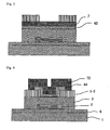
- the thin film field effect transistor of the invention is an active element which has at least a gate electrode, a gate insulating layer, an active layer, a source electrode and a drain electrode in this order, and has a function of switching current between the source electrode and the drain electrode, in which a current passing through the active layer is controlled by applying voltage to the gate electrode.
- the TFT structure either of a stagger structure and a reversed stagger structure may be formed.
- an amorphous oxide semiconductor of the active layer contains at least one selected from the group consisting of In, Ga, Zn and Sn. More preferably, the amorphous oxide semiconductor of the active layer contains In and Zn.
- a more preferable embodiment of the active layer in the invention is a configuration where a low carrier concentration layer that has a carrier concentration of 10 16 cm -3 or less is laminated in contact with the active layer on the opposite side of the active layer from the gate insulating layer.
- the low carrier concentration layer as well is an amorphous oxide semiconductor layer. It is preferred that the amorphous oxide semiconductor of the low carrier concentration layer contains at least one selected from the group consisting of In, Ga, Zn and Sn. More preferably, the amorphous oxide semiconductor of the low carrier concentration layer contains In and Zn.
- the low carrier concentration layer according to the invention is a material system that is approximate to the active layer, so the active layer is hardly damaged at the time of film formation by sputtering. In the case where film formation is conducted by sputtering using conventional SiO 2 as a protective layer, the active layer is easily damaged.
- the low carrier concentration layer according to the invention has a carrier concentration that is an order of magnitude lower than the carrier concentration of the active layer and has high insulating property, the high carrier concentration of the active layer can be stably maintained, and therefore, the effects of the active layer can be stably maintained without being hindered.
- the low carrier concentration layer according to the invention also functions as a protective layer that protects the active layer from environment (moisture, oxygen).
- the low carrier concentration layer can be made thick as compared with the active layer and is an oxide film, it suppresses diffusion of moisture or oxygen to the active layer and can prevent a change in carrier concentration of the active layer during storage.
- the active layer is made to be a thin layer having a film thickness of 0.5 nm or more and less than 10 nm
- the roughness of an interface between the gate insulating layer and the active layer largely affects on TFT performance, and it is found very important to maintain the roughness of the interface at less than 2 nm.
- the substrate is a flexible resin substrate.
- an amorphous oxide semiconductor As an amorphous oxide semiconductor film can be formed at a low temperature, it can be prepared on a flexible resin substrate made of plastic.
- the amorphous oxide semiconductor which can be prepared at a low temperature include an oxide containing In, an oxide containing In and Zn, and an oxide containing In, Ga and Zn.
- amorphous oxide semiconductors of InGaO 3 (ZnO) m (m is a natural number less than 6) are preferable. These amorphous oxide semiconductors are n-type semiconductors, in which electrons serve as carriers.
- Oxide semiconductors disclosed in JP-A No. 2006-165529 can also be used.
- an amorphous oxide semiconductor containing at least one selected from the group consisting of In, Ga, Zn and Sn is preferred.
- An amorphous oxide semiconductor containing In and Zn is more preferred.
- the amorphous oxide semiconductor in the invention has a constitution including In-Ga-Zn-O, and preferably a composition of InGaO 3 (ZnO) m (m is a natural number less than 6) in a crystalline state. Particularly, InGaZnO 4 is preferable.
- An amorphous oxide semiconductor of such composition has a feature that electron mobility tends to increase with an increase in electric conductivity.
- the electric conductivity can be controlled by controlling the partial pressure of oxygen during film formation.
- oxide semiconductors not only oxide semiconductors, but also inorganic semiconductors such as Si and Ge, compound semiconductors such as GaAs, and organic semiconductor materials such as pentacene and polythiophene, carbon nanotube, or the like can be applied.
- inorganic semiconductors such as Si and Ge
- compound semiconductors such as GaAs
- organic semiconductor materials such as pentacene and polythiophene, carbon nanotube, or the like can be applied.
- a carrier concentration of the active layer in the invention is controlled to a desired value by several means.
- the carrier concentration of an oxide semiconductor can be controlled by adjusting the quantity of oxygen vacancies.
- methods for controlling the quantity of oxygen vacancies include adjusting the partial pressure of oxygen during film formation, and oxygen concentration and treatment time of an after-treatment after the film formation.
- examples of the after-treatment include heat treatment at a temperature of 100°C or higher, processing by oxygen plasma, and UV ozone treatment.
- the method involving controlling the partial pressure of oxygen during film formation is preferable in view of its productivity.
- the carrier concentration of an oxide semiconductor can be controlled by adjusting the partial pressure of oxygen during film formation.
- the carrier concentration can be changed by changing the composition ratio of metals of an oxide semiconductor. For instance, in the case of InGaZn 1-x Mg x O 4 , the carrier concentration lowers with an increase in the percentage of Mg. In addition, it has been reported that the carrier concentration of oxides of (In 2 O 3 ) 1-x (ZnO) x lowers with an increase in the percentage of Zn when the Zn/In ratio is 10% or higher.
- methods for changing the composition ratio for example in the case of a method of forming a film by sputtering include a method using targets with different composition ratios. Alternatively, multiple targets may be co-sputtered, changing the composition ratio of the resultant film by individually adjusting the sputtering rates for the targets.
- the carrier concentration can be reduced.
- Methods for adding an impurity include co-vapor deposition of the oxide semiconductor and the impurity, and ion-doping of an oxide semiconductor film which has already been formed with ions of the impurity element.
- the carrier concentration can be changed by changing the oxide semiconductor material. It is known that the carrier concentration of SnO 2 -based oxide semiconductors is lower than the carrier concentration of In 2 O 3 -based oxide semiconductors. In this way, the carrier concentration can be adjusted by changing the oxide semiconductor material.
- the methods stated in the above (1) to (4) may be used independently or in combination.
- a vapor-phase film forming method using, as a target, a polycrystalline sintered body of an oxide semiconductor.
- sputtering method and pulsed laser deposition method PLD method
- PLD method pulsed laser deposition method
- mass production sputtering method is preferable.
- a film can be formed while controlling the vacuum level and flow rate of oxygen.
- the active layer in the invention is a very thin layer.
- the uniformity of an interface between the active layer and an adjacent layer to which the active layer is disposed is important.
- an active layer is disposed on a gate insulating layer.
- it is desirable that an interface between the gate insulating layer and the active layer is smooth, preferably less than 2 nm in the interface roughness and more preferably less than 1 nm.
- film-formation speeds of the gate insulating layer and the active layer are preferably controlled by the sputtering speed and deposition speed of the respective film components to find a condition for forming a uniform film to carry out.
- composition ratio can be determined by RBS analysis (Rutherford Backscattering Spectrometry).
- the active layer in the present invention is very thin, and the thickness of the active layer is from 0.5 nm or more and less than 10 nm.
- the thickness of the active layer can be determined by HRTEM (High Resolution Transmittance Electron Micrograph) photograph of a section of the prepared element.
- Use of the active layer arranged as described above achieves a TFT characterized by an ON-OFF ratio of 10 6 or higher and high mobility of 10 cm 2 /Vs or higher.
- a multilayer structure where a low carrier concentration layer that has a carrier concentration of 10 16 cm -3 or less, which is lower than the carrier concentration of the active layer, is laminated in contact with the active layer on the opposite side of the active layer from the gate insulating layer is preferred.
- a semiconductor material used in the low carrier concentration layer as well is preferred to be an amorphous oxide.
- the carrier concentration of the low carrier concentration layer is preferably 10 15 cm -3 or less, and more preferably 10 14 cm -3 or less.
- a ratio of the electric conductivity of the active layer to the electric conductivity of the low carrier concentration layer is preferably from 10 1 to 10 10 , and more preferably from 10 2 to 10 8 .
- the semiconductor material used in the low carrier concentration layer may be selected from materials described of materials of the active layer to use.
- the carrier concentration as well may be controlled by similar means described of the control means of a carrier concentration in the active layer.
- a thickness of the low carrier concentration layer is not particularly limited, but is approximately in a range of from 0.5 nm to 100 nm and preferably in a range of from 1 nm to 50 nm.
- the following materials are among those which are preferable for the gate electrode: a metal such as Al, Mo, Cr, Ta, Ti, Au or Ag, an alloy such as Al-Nd or APC; a metal oxide electrically conductive film of e.g., tin oxide, zinc oxide, indium oxide, indium-tin oxide (ITO), or indium-zinc oxide (IZO); an organic electrically conductive compound such as polyaniline, polythiophene, or polypyrrole; or a mixture thereof.
- a metal such as Al, Mo, Cr, Ta, Ti, Au or Ag, an alloy such as Al-Nd or APC
- an organic electrically conductive compound such as polyaniline, polythiophene, or polypyrrole; or a mixture thereof.
- the thickness of the gate electrode is preferably from 10 nm to 1000 nm.
- the method of forming the gate electrode is not particularly limited.
- the gate electrode can be formed on the substrate according to a method which is appropriately selected from among wet methods such as a printing method and a coating method, physical methods such as a vacuum deposition method, a sputtering method and an ion plating method, chemical methods such as a chemical vapor deposition (CVD) and plasma CVD method, and the like in consideration of the suitability to the material described above.
- the gate electrode can be formed according to a direct current or high-frequency sputtering method, a vacuum deposition method, or an ion plating method.
- the film formation of the gate electrode can be performed according to a wet film-forming method.
- an insulator such as SiO 2 , SiN x , SiON, Al 2 O 3 , Y 2 O 3 , Ta 2 O 5 , HfO 2 or the like, or a mixed crystal compound containing at least two of these is used.
- a polymeric insulator such as polyimide may be used for the gate insulating layer.
- the gate insulating layer has a thickness of from 10 nm to 10 ⁇ m. To reduce the leak current and raise the voltage resistance, it is required to make the gate insulating layer thicker to a certain extent. However, an increase in the thickness of the gate insulating layer results in a rise in the voltage needed for driving the TFT. Therefore, it is preferable that the thickness of the gate insulating layer is from 50 nm to 1000 nm for an inorganic insulator, and from 0.5 ⁇ m to 5 ⁇ m for a polymeric insulator. Especially, it is particularly preferable to use an insulator with a high dielectric constant, such as HfO 2 , for the gate insulating layer, because then the TFT can be driven with low voltage even when it is made thicker.
- a high dielectric constant such as HfO 2
- the following are suitable for the material of the source electrode and the drain electrode: metals such as A1, Mo, Cr, Ta, Ti, Au and Ag; alloys such as Al-Nd and APC; metal oxide electrically conductive films of, for example, tin oxide, zinc oxide, indium oxide, indium-tin oxide (ITO) and indium-zinc oxide (IZO); and organic electrically conductive compounds such as polyaniline, polythiophene and polypyrrole, and mixtures thereof.
- metals such as A1, Mo, Cr, Ta, Ti, Au and Ag
- alloys such as Al-Nd and APC
- organic electrically conductive compounds such as polyaniline, polythiophene and polypyrrole, and mixtures thereof.
- the thickness of the source electrode and the drain electrode is preferably from 10 nm to 1000 nm.
- the method of forming the source electrode and drain electrode is not particularly limited.
- the electrodes can be formed on the substrate according to a method which is appropriately selected from among wet methods such as a printing method and a coating method, physical methods such as a vacuum deposition method, a sputtering method and an ion plating method, chemical methods such as a CVD and plasma CVD method, and the like in consideration of the suitability to the material described above.
- wet methods such as a printing method and a coating method
- physical methods such as a vacuum deposition method, a sputtering method and an ion plating method, chemical methods such as a CVD and plasma CVD method, and the like in consideration of the suitability to the material described above.
- the electrodes can be formed according to a direct current or high-frequency sputtering method, a vacuum deposition method, an ion plating method, etc.
- the film formation of the source electrode and drain electrode can be performed according to a wet film-forming method.
- the substrate used herein is not particularly limited.
- the following materials are for example suitable for the substrate: inorganic materials such as YSZ (zirconia stabilized yttrium) and glass; and organic materials including polyesters such as polyethylene terephthalate, polybutylene terephthalate and polyethylene naphthalate, and synthetic resins such as polystyrene, polycarbonate, polyether sulfone, polyarylate, allyl diglycol carbonate, polyimide, polycycloolefin, norbornene resin, and polychlorotrifluoroethylene.
- inorganic materials such as YSZ (zirconia stabilized yttrium) and glass
- organic materials including polyesters such as polyethylene terephthalate, polybutylene terephthalate and polyethylene naphthalate, and synthetic resins such as polystyrene, polycarbonate, polyether sulfone, polyarylate, allyl diglycol carbonate, polyimide,
- a flexible substrate As for the material used for the flexible substrate, an organic plastic film which has high transmittance is preferable.
- the following materials can be used: polyesters such as polyethylene terephthalate, polybutylene phthalate and polyethylene naphthalate; and plastic films such as polystyrene, polycarbonate, polyether sulfone, polyarylate, polyimide; polycycloolefin, norbornene resin, and polychlorotrifluoroethylene.
- such film-shaped plastic substrate has an insulating layer in the case where the insulation is insufficient, a gas-barrier layer for preventing moisture and oxygen from penetrating through the substrate, or an undercoat layer for enhancing planarity and adhesion with the electrode or active layer of the film-shaped plastic substrate.
- the thickness of the flexible substrate is from 50 ⁇ m to 500 ⁇ m. The reason for this is that when the thickness of the flexible substrate is less than 50 ⁇ m, it is hard for the substrate to maintain sufficient planarity itself, and when the flexible substrate is thicker than 500 ⁇ m, it becomes difficult to bend the substrate itself freely, i.e., the flexibility of the substrate becomes insufficient.
- a source electrode and a drain electrode are not disposed directly on a thin active layer, and therefore, the active layer does not suffer from damages during a process providing the source electrode and drain electrode.
- the active layer 44 is protected from an environmental action (moisture or oxygen), and therefore, in the case where, after the formation of the source electrode and drain electrode, an organic EL element part is disposed thereon, the active layer does not suffer from damages during the process.
- Fig. 5 is a schematic diagram of an equivalent circuit of an active matrix-driving type organic EL display which uses the TFT element of the invention.
- the circuit of the organic EL display according to the invention is not particularly limited to that shown in Fig. 5 .
- a circuit which is conventionally known in the art may be applied as-is.
- the thin film field effect transistor of the invention is preferably used for an image display with a liquid crystal or EL element incorporated therein, and particularly for a flat panel display (FPD). More preferably, it is used for a flexible display in which a flexible substrate such as an organic plastic film is used as its substrate. Particularly, the thin film field effect transistor of the invention has high mobility, and therefore it is most preferably used for a display incorporating an organic EL element, a flexible organic EL display.
- the organic EL display of the invention includes, on a substrate, an organic EL element having at least a lower electrode, an organic compound layer containing at least a light-emitting layer and an upper electrode, in this order, and a TFT for driving the organic EL element having at least a gate electrode, a gate insulating layer, an active layer containing an oxide semiconductor, a source electrode, and a drain electrode on the upper electrode. Since the TFT is disposed at a back side of the organic EL element, an aperture for extracting light emission of the organic EL element can be made larger.
- a protective insulating layer is disposed between the TFT and the organic EL element, and the upper electrode of the organic EL element and the source electrode or the drain electrode of the TFT are electrically connected by way of a contact hole formed in the protective insulating layer.
- the lower electrode is a light transmitting electrode and the upper electrode is a light reflective electrode.
- the light-emitting element according to the invention has a cathode and an anode on a substrate, and an organic compound layer containing an organic light-emitting layer (hereinafter, sometimes simply referred to as a "light-emitting layer") between the two electrodes. Due to the nature of a light-emitting element, at least one electrode of the anode and the cathode is preferably transparent.
- the layer includes a hole transport layer, a light-emitting layer, and an electron transport layer integrated in this order from the anode side.
- a hole injection layer is provided between the hole transport layer and the anode, and/or an electron transporting intermediate layer is provided between the light-emitting layer and the electron transport layer.
- a hole transporting intermediate layer may be provided between the light-emitting layer and the hole transport layer, and similarly, an electron injection layer may be provided between the cathode and the electron transport layer.
- each of the layers may be composed of plural secondary layers.
- the respective layers constituting the organic compound layer can be suitably formed in accordance with any of a dry film-forming method such as a vapor deposition method, or a sputtering method; a transfer method; a printing method; a coating method; an ink-jet method; a spray method; or the like.
- a dry film-forming method such as a vapor deposition method, or a sputtering method
- a transfer method such as a vapor deposition method, or a sputtering method
- a transfer method such as a vapor deposition method, or a sputtering method
- a printing method such as a a coating method, an ink-jet method; a spray method; or the like.
- the substrate to be applied in the invention is preferably one which does not scatter or attenuate light emitted from the organic compound layer.
- materials for the substrate include inorganic materials such as zirconia-stabilized yttrium (YSZ), glass and the like; and organic materials such as, for example, polyesters such as polyethylene terephthalate, polybutylene phthalate, and polyethylene naphthalate, polystyrene, polycarbonate, polyethersulfone, polyarylate, polyimide, polycycloolefin, norbornene resin, polychlorotrifluoroethylene, and the like.
- non-alkali glass is preferably used with respect to the quality of material in order to decrease ions eluted from the glass.
- soda-lime glass it is preferred to use glass on which a barrier coat of silica or the like has been applied.
- an organic material it is preferred to use a material excellent in heat resistance, dimensional stability, solvent resistance, electric insulating property, and workability.
- a structure of the substrate may be a monolayer structure or a laminated structure.
- the substrate may be formed from a single member or two or more members.
- the substrate may be transparent and colorless, or transparent and colored, it is preferred that the substrate is transparent and colorless from the viewpoint that the substrate does not scatter or attenuate light emitted from the organic light-emitting layer.
- a moisture permeation preventive layer may be provided on the front surface or the back surface of the substrate.
- the moisture permeation preventive layer For a material of the moisture permeation preventive layer (gas barrier layer), inorganic substances such as silicon nitride and silicon oxide may be preferably applied.
- the moisture permeation preventive layer (gas barrier layer) may be formed in accordance with, for example, a high-frequency sputtering method or the like.
- thermoplastic substrate In the case of applying a thermoplastic substrate, a hard-coat layer or an undercoat layer may be further provided as needed.
- the anode may generally be any material as long as it has a function as an electrode for supplying holes to the organic compound layer, and there is no particular limitation as to the shape, the structure, the size or the like. However, it may be suitably selected from among well-known electrode materials according to the application and purpose of the light-emitting element. As mentioned above, the anode is usually provided as a transparent anode.
- Materials for the anode preferably include, for example, metals, alloys, metal oxides, electrically conductive compounds, and mixtures thereof.
- Specific examples of the anode materials include electrically conductive metal oxides such as tin oxides doped with antimony, fluorine or the like (ATO and FTO), tin oxide, zinc oxide, indium oxide, indium tin oxide (ITO), and indium zinc oxide (IZO); metals such as gold, silver, chromium, and nickel; mixtures or laminates of these metals and the electrically conductive metal oxides; inorganic electrically conductive materials such as copper iodide and copper sulfide; organic electrically conductive materials such as polyaniline, polythiophene, and polypyrrole; and laminates of these inorganic or organic electrically conductive materials with ITO.
- the electrically conductive metal oxides are preferred, and particularly, ITO is preferable in view of productivity, high electric conductivity, transparency and the like.
- the anode may be formed on the substrate in accordance with a method which is appropriately selected from among wet methods such as a printing method, a coating method and the like; physical methods such as a vacuum deposition method, a sputtering method, an ion plating method and the like; and chemical methods such as a CVD and plasma CVD method and the like, in consideration of the suitability to a material constituting the anode.
- a method which is appropriately selected from among wet methods such as a printing method, a coating method and the like; physical methods such as a vacuum deposition method, a sputtering method, an ion plating method and the like; and chemical methods such as a CVD and plasma CVD method and the like, in consideration of the suitability to a material constituting the anode.
- wet methods such as a printing method, a coating method and the like
- physical methods such as a vacuum deposition method, a sputtering method, an ion plating method and the like
- a position at which the anode is to be formed is not particularly limited, and it may be suitably selected according to the application and purpose of the light-emitting element.
- the anode is preferably formed on the substrate. In this case, the anode may be formed on either the whole surface or a part of the surface on either side of the substrate.
- a chemical etching method such as photolithography, a physical etching method such as etching by laser, a method of vacuum deposition or sputtering through superposing masks, or a lift-off method or a printing method may be applied.
- a thickness of the anode may be suitably selected according to the material constituting the anode and is therefore not definitely decided, but it is usually in a range of from 10 nm to 50 ⁇ m, and preferably from 50 nm to 20 ⁇ m.
- a value of electric resistance of the anode is preferably 10 3 ⁇ / ⁇ or less, and more preferably 10 2 ⁇ / ⁇ or less.
- the anode may be either transparent and colorless, or transparent and colored.
- a light transmittance of the anode is 60% or higher, and more preferably 70% or higher.
- the cathode may generally be any material as long as it has a function as an electrode for injecting electrons to the organic compound layer, and there is no particular limitation as to the shape, the structure, the size or the like. However it may be suitably selected from among well-known electrode materials according to the application and purpose of the light-emitting element.
- Materials constituting the cathode include, for example, metals, alloys, metal oxides, electrically conductive compounds, and mixtures thereof. Specific examples thereof include alkali metals (e.g., Li, Na, K, Cs or the like), alkaline earth metals (e.g., Mg, Ca or the like), gold, silver, lead, aluminum, sodium-potassium alloys, lithium-aluminum alloys, magnesium-silver alloys, rare earth metals such as indium, and ytterbium, and the like. They may be used alone, but it is preferred that two or more of them are used in combination from the viewpoint of satisfying both stability and electron inject-ability.
- alkali metals e.g., Li, Na, K, Cs or the like
- alkaline earth metals e.g., Mg, Ca or the like
- alkaline metals or alkaline earth metals are preferred in view of electron inject-ability, and materials containing aluminum as a major component are preferred in view of excellent preservation stability.
- material containing aluminum as a major component refers to a material constituted by aluminum alone; alloys comprising aluminum and 0.01% by weight to 10% by weight of an alkaline metal or an alkaline earth metal; or the mixtures thereof (e.g., lithium-aluminum alloys, magnesium-aluminum alloys and the like).
- a method for forming the cathode is not particularly limited, but it may be formed in accordance with a well-known method.
- the cathode may be formed in accordance with a method which is appropriately selected from among wet methods such as a printing method, a coating method and the like; physical methods such as a vacuum deposition method, a sputtering method, an ion plating method and the like; and chemical methods such as a CVD and plasma CVD method and the like, in consideration of the suitability to a material constituting the cathode.
- a metal or metals
- one or two or more of them may be applied at the same time or sequentially in accordance with a sputtering method or the like.
- a chemical etching method such as photolithography, a physical etching method such as etching by laser, a method of vacuum deposition or sputtering through superposing masks, or a lift-off method or a printing method may be applied.
- a position at which the cathode is to be formed is not particularly limited, and it may be formed on either the whole or a part of the organic compound layer.
- a dielectric material layer made of fluorides, oxides or the like of an alkaline metal or an alkaline earth metal may be inserted between the cathode and the organic compound layer with a thickness of from 0.1 nm to 5 nm.
- the dielectric layer may be considered to be a kind of electron injection layer.
- the dielectric material layer may be formed in accordance with, for example, a vacuum deposition method, a sputtering method, an ion-plating method or the like.
- a thickness of the cathode may be suitably selected according to materials for constituting the cathode and is therefore not definitely decided, but it is usually in a range of from 10 nm to 5 ⁇ m, and preferably from 50 nm to 1 ⁇ m.
- the cathode may be transparent or opaque.
- the transparent cathode may be formed by preparing a material for the cathode with a small thickness of 1 nm to 10 nm, and further laminating a transparent electrically conductive material such as ITO or IZO thereon.
- the organic compound layer according to the present invention is to be described.
- the organic EL element according to the present invention has at least one organic compound layer including a light-emitting layer.
- An organic compound layer apart from the light-emitting layer comprises a hole transport layer, an electron transport layer, a hole blocking layer, an electron blocking layer, a hole injection layer, an electron injection layer and the like as described above.
- the respective layers constituting the organic compound layer can be suitably formed in accordance with any of a dry film-forming method such as a vapor deposition method, or a sputtering method; a wet film-forming method; a transfer method; a printing method; an ink-jet method; or the like.
- the organic light-emitting layer is a layer having functions of receiving holes from the anode, the hole injection layer, or the hole transport layer, and receiving electrons from the cathode, the electron injection layer, or the electron transport layer, and providing a field for recombination of the holes with the electrons to emit light, when an electric field is applied to the layer.
- the light-emitting layer according to the present invention may contain only a light-emitting material, or may be a mixture layer containing a light-emitting dopant and a host material.
- the light-emitting dopant may be a fluorescent light-emitting material or a phosphorescent light-emitting material, and may be a plurality of those compounds.
- the host material is a charge-transporting material.
- the host material may be one or a plurality of compounds. For example, a mixture of a hole-transporting host material and an electron-transporting host material is preferable. Further, a material which does not emit light nor transport any charge may be contained in the light-emitting layer.
- the light-emitting layer may be a single layer or a plurality of layers, wherein the respective layers may emit light of different color from one another.
- any of a fluorescent light-emitting material and a phosphorescent light-emitting material may be used as a light-emitting dopant.
- the light-emitting layer according to the present invention may contain two or more types of light-emitting dopants for improving color purity and expanding the wavelength region of emitted light. It is preferred that the light-emitting dopant in the present invention is one satisfying a relationship between the above-described host material and the light-emitting dopant of 1.2 eV > the difference of Ip between host material and light-emitting dopant ( ⁇ Ip) > 0.2 eV and/or 1.2 eV > the difference of Ea between host material and light-emitting dopant ( ⁇ Ea) > 0.2 eV in view of drive durability.
- Examples of the phosphorescent light-emitting dopants generally include complexes containing a transition metal atom or a lanthanoid atom.
- the transition metal atom is not limited, it is preferably ruthenium, rhodium, palladium, tungsten, rhenium, osmium, iridium, gold, silver, copper or platinum; more preferably rhenium, iridium, or platinum, and even more preferably iridium or platinum.
- lanthanoid atom examples include lanthanum, cerium, praseodymium, neodymium, samarium, europium, gadolinium, terbium, dysprosium, holmium, erbium, thulium, ytterbium, and lutetium, and among these lanthanoid atoms, neodymium, europium, and gadolinium are preferred.
- ligands in the complex include the ligands described, for example, in " Comprehensive Coordination Chemistry” authored by G. Wilkinson et al., published by Pergamon Press Company in 1987 ; " Photochemistry and Photophysics of Coordination Compounds” authored by H. Yersin, published by Springer-Verlag Company in 1987 ; and " YUHKI KINZOKU KAGAKU -KISO TO OUYOU- (Organometallic Chemistry -Fundamental and Application-)” authored by Akio Yamamoto, published by Shokabo Publishing Co., Ltd. in 1982 .
- the ligand preferably include halogen ligand (preferably, chlorine ligand), aliphatic carbocyclic ring ligand (for example, having preferably 5 to 30 carbon atoms, more preferably 6 to 30 carbon atoms, further preferably 6 to 20 carbon atoms, and particularly preferably 6 to 12 carbon atoms, such as cyclopentadienyl anion, benzene anion, naphthyl anion, or the like), nitrogen-containing heterocyclic ligand (for example, having preferably 5 to 30 atoms, more preferably 6 to 30 carbon atoms, further preferably 6 to 20 carbon atoms, and particularly preferably 6 to 12 carbon atoms, for example, phenyl pyridine, benzoquinoline, quinolinol, bipyridyl, phenanthrorine, or the like), diketone ligand (for example, acetyl acetone, or the like), carboxylic acid ligand (for example, having preferably 2 to
- the above-described complexes may be either a complex containing one transition metal atom in the compound, or a so-called polynuclear complex containing two or more transition metal atoms wherein different metal atoms may be contained at the same time.
- the light-emitting dopants include phosphorescent light-emitting compounds described in patent documents such as U.S.Patent ( USP) Nos. 6303238B1 , and 6097147 ; International Patent Publication ( WO) Nos. 00/57676 , 00/70655 , 01/08230 , 01/39234A2 , 01/41512A1 , 02/02714A2 , 02/15645A1 , 02/44189A1 , and 05/19373A2 ; JP-A Nos.
- the light-emitting dopants include Ir complexes, Pt complexes, Cu complexes, Re complexes, W complexes, Rh complexes, Ru complexes, Pd complexes, Os complexes, Eu complexes, Tb complexes, Gd complexes, Dy complexes, and Ce complexes; particularly preferable are Ir complexes, Pt complexes, and Re complexes; and among these, Ir complexes, Pt complexes, and Re complexes each containing at least one coordination mode of metal-carbon bonds, metal-nitrogen bonds, metal-oxygen bonds, and metal-sulfur bonds are preferred. Particularly preferably, Ir complexes, Pt complexes, and Re complexes each containing a tri- or higher-dentate ligand are preferred in view of light-emission efficiency, drive durability, color purity and the like.
- Examples of the above-described fluorescent light-emitting dopants generally include benzoxazole, benzimidazole, benzothiazole, styrylbenzene, polyphenyl, diphenylbutadiene, tetraphenylbutadiene, naphthalimide, coumarin, pyran, perinone, oxadiazole, aldazine, pyralidine, cyclopentadiene, bis-styrylanthracene, quinacridone, pyrrolopyridine, thiadiazolopyridine, cyclopentadiene, styrylamine, aromatic dimethylidene compounds, condensed polycyclic aromatic compounds (anthracene, phenanthroline, pyrene, perylene, rubrene, pentacene and the like), a variety of metal complexes represented by metal complexes of 8-quinolinol, pyromethene complexes or rare-earth complexe
- light-emitting dopants include the following compounds, but it should be noted that the present invention is not limited thereto.
- the light-emitting dopant in the light-emitting layer is contained in an amount of from 0.1% by weight to 50% by weight with respect to the total weight of the compounds generally forming the light-emitting layer, but it is preferably contained in an amount of from 1% by weight to 50% by weight, and more preferably in an amount of from 2% by weight to 40% by weight in view of drive durability and external quantum efficiency.
- a thickness of the light-emitting layer is not particularly limited, 2 nm to 500 nm is usually preferred, and within this range, 3 nm to 200 nm is more preferable, and 5 nm to 100 nm is even more preferred in view of external quantum efficiency.
- hole transporting host materials excellent in hole transporting property referred to as a "hole transporting host” in some cases
- electron transporting host compounds excellent in electron transporting property referred to as an “electron transporting host” in some cases
- hole transporting hosts used in the present invention include pyrrole, indole, carbazole, azaindole, azacarbazole, triazole, oxazole, oxadiazole, pyrazole, imidazole, thiophene, polyarylalkane, pyrazoline, pyrazolone, phenylenediamine, arylamine, amino-substituted chalcone, styrylanthracene, fluorenone, hydrazone, stilbene, silazane, aromatic tertiary amine compounds, styrylamine compounds, aromatic dimethylidine compounds, porphyrin compounds, polysilane compounds, poly(N-vinylcarbazole), aniline copolymers, electrically conductive high-molecular oligomers such as thiophene oligomers, polythiophenes and the like, organic silanes, carbon films, derivatives thereof, and the like.
- indole derivatives carbazole derivatives, aromatic tertiary amine compounds, and thiophene derivatives are preferable, and compounds containing a carbazole group in the molecule are more preferable. Particularly, compounds containing t-butyl substituted carbazole group are preferred.
- an electron affinity Ea of the host is from 2.5 eV to 3.5 eV, more preferably from 2.6 eV to 3.4 eV, and even more preferably from 2.8 eV to 3.3 eV in view of improvements in durability and decrease in drive voltage.
- an ionization potential Ip of the host is 5.7 eV to 7.5 eV, more preferably 5.8 eV to 7.0 eV, and even more preferably 5.9 eV to 6.5 eV in view of improvements in drive durability and decrease in drive voltage.
- electron transporting hosts include pyridine, pyrimidine, triazine, imidazole, pyrazole, triazole, oxazole, oxadiazole, fluorenone, anthraquinonedimethane, anthrone, diphenylquinone, thiopyrandioxide, carbodiimide, fluorenylidenemethane, distyrylpyrazine, fluorine-substituted aromatic compounds, aromacyclic tetracarboxylic anhydrides of naphthalene, perylene or the like, phthalocyanine, derivatives thereof (which may form a condensed ring with another ring), and a variety of metal complexes represented by metal complexes of 8-quinolinol derivatives, metal phthalocyanine, and metal complexes having benzoxazole or benzothiazole as the ligand.
- Preferable electron transporting hosts are metal complexes, azole derivatives (benzimidazole derivatives, imidazopyridine derivatives and the like), and azine derivatives (pyridine derivatives, pyrimidine derivatives, triazine derivatives and the like).
- metal complex compounds are preferred in the present invention in view of durability.
- a metal complex containing a ligand having at least one nitrogen atom, oxygen atom, or sulfur atom to be coordinated with the metal is more preferable.
- a metal ion in the metal complex is not particularly limited, a beryllium ion, a magnesium ion, an aluminum ion, a gallium ion, a zinc ion, an indium ion, a tin ion, a platinum ion, or a palladium ion is preferred; more preferable is a beryllium ion, an aluminum ion, a gallium ion, a zinc ion, a platinum ion, or a palladium ion; and even more preferable is an aluminum ion, a zinc ion, or a palladium ion.
- ligands include ligands described in " Photochemistry and Photophysics of Coordination Compounds" authored by H. Yersin, published by Springer-Verlag Company in 1987 ; " YUHKI KINZOKU KAGAKU -KISO TO OUYOU- (Organometallic Chemistry -Fundamental and Application-)” authored by Akio Yamamoto, published by Shokabo Publishing Co., Ltd. in 1982 , and the like.
- the ligands are preferably nitrogen-containing heterocyclic ligands (having preferably 1 to 30 carbon atoms, more preferably 2 to 20 carbon atoms, and particularly preferably 3 to 15 carbon atoms); and they may be a unidentate ligand or a bi- or higher-dentate ligand.
- nitrogen-containing heterocyclic ligands having preferably 1 to 30 carbon atoms, more preferably 2 to 20 carbon atoms, and particularly preferably 3 to 15 carbon atoms
- they may be a unidentate ligand or a bi- or higher-dentate ligand.
- Preferable are bi- to hexa-dentate ligands, and mixed ligands of bi- to hexa-dentate ligands with a unidentate ligand are also preferable.
- ligands examples include azine ligands (e.g., pyridine ligands, bipyridyl ligands, terpyridine ligands and the like); hydroxyphenylazole ligands (e.g., hydroxyphenylbenzimidazole ligands, hydroxyphenylbenzoxazole ligands, hydroxyphenylimidazole ligands, hydroxyphenylimidazopyridine ligands and the like); alkoxy ligands (those having preferably 1 to 30 carbon atoms, more preferably 1 to 20 carbon atoms, and particularly preferably 1 to 10 carbon atoms, examples of which include methoxy, ethoxy, butoxy, 2-ethylhexyloxy and the like); aryloxy ligands (those having preferably 6 to 30 carbon atoms, more preferably 6 to 20 carbon atoms, and particularly preferably 6 to 12 carbon atoms, examples of which include
- nitrogen-containing heterocyclic ligands, aryloxy ligands, heteroaryloxy groups, aromatic hydrocarbon anion ligands, aromatic heterocyclic anion ligands or siloxy ligands are preferable, and nitrogen-containing heterocyclic ligands, aryloxy ligands, siloxy ligands, aromatic hydrocarbon anion ligands, or aromatic heterocyclic anion ligands are more preferable.
- metal complex electron transporting hosts examples include compounds described, for example, in JP-A Nos. 2002-235076 , 2004-214179 , 2004-221062 , 2004-221065 , 2004-221068 , 2004-327313 and the like.
- the lowest triplet excitation level T1 of the host material is higher than T1 of the phosphorescent light-emitting material in view of color purity, light-emission efficiency, and drive durability.
- a content of the host compounds according to the present invention is not particularly limited, it is preferably 15% by weight to 95% by weight with respect to the total weight of the compounds forming the light-emitting layer in view of light-emission efficiency and drive voltage.
- the hole injection layer and hole transport layer correspond to layers functioning to receive holes from an anode or from an anode side and to transport the holes to a cathode side.
- Materials to be introduced into a hole injection layer or a hole transport layer is not particularly limited, but either of a low molecular compound or a high molecular compound may be used.
- the hole injection layer and the hole transport layer it is preferred to contain specifically pyrrole derivatives, carbazole derivatives, triazole derivatives, oxazole derivatives, oxadiazole derivatives, imidazole derivatives, polyarylalkane derivatives, pyrazoline derivatives, pyrazolone derivatives, phenylenediamine derivatives, arylamine derivatives, amino-substituted chalcone derivatives, styrylanthracene derivatives, fluorenone derivatives, hydrazone derivatives, stilbene derivatives, silazane derivatives, aromatic tertiary amine compounds, styrylamine compounds, aromatic dimethylidine compounds, phthalocyanine compounds, porphyrin compounds, thiophene derivatives, organic silane derivatives, carbon, or the like.
- An electron-accepting dopant may be introduced into the hole injection layer or the hole transport layer in the organic EL element according to the present invention.
- the electron-accepting dopant to be introduced into the hole injection layer or the hole transport layer either of an inorganic compound or an organic compound may be used as long as the compound has electron accepting property and a function for oxidizing an organic compound.
- the inorganic compound includes metal halides, such as iron (III) chloride, aluminum chloride, gallium chloride, indium chloride and antimony pentachloride and the like, and metal oxides, such as vanadium pentaoxide, molybdenum trioxide and the like.
- metal halides such as iron (III) chloride, aluminum chloride, gallium chloride, indium chloride and antimony pentachloride and the like
- metal oxides such as vanadium pentaoxide, molybdenum trioxide and the like.
- These electron-accepting dopants may be used alone or in a combination of two or more of them. Although an applied amount of these electron-accepting dopants depends on the type of material, 0.01% by weight to 50% by weight of a dopant is preferred with respect to a hole transport layer material, 0.05% by weight to 20% by weight is more preferable, and 0.1% by weight to 10% by weight is particularly preferred.
- a thickness of the hole injection layer and the hole transport layer is preferably 500 nm or less in view of decrease in drive voltage.
- a thickness of the hole transport layer is preferably from 1 nm to 500 nm, more preferably from 5 nm to 200 nm, and even more preferably from 10 nm to 100 nm.
- a thickness of the hole injection layer is preferably from 0.1 nm to 200 nm, more preferably from 0.5 nm to 100 nm, and even more preferably from 1 nm to 100 nm.
- the hole injection layer and the hole transport layer may be composed of a monolayer structure comprising one or two or more of the above-mentioned materials, or a multilayer structure composed of plural layers of a homogeneous composition or a heterogeneous composition.
- An electron injection layer and an electron transport layer are layers having any of functions for receiving electrons from a cathode or a cathode side, and transporting electrons to an anode side.
- An electron injection material or an electron transport material to be introduced therein may be a low molecular compound or a high molecular compound.
- the materials include pyridine derivatives, quinoline derivatives, pyrimidine derivatives, pyrazine derivatives, phthalazine derivatives, phenanthoroline derivatives, triazine derivatives, triazole derivatives, oxazole derivatives, oxadiazole derivatives, imidazole derivatives, fluorenone derivatives, anthraquinodimethane derivatives, anthrone derivatives, diphenylquinone derivatives, thiopyrandioxide derivatives, carbodiimide derivatives, fluorenylidenemethane derivatives, distyrylpyradine derivatives, aromacyclic tetracarboxylic anhydrides of perylene or naphthalene, phthalocyanine derivatives, metal complexes represented by metal complexes of 8-quinolinol derivatives, metal phthalocyanine, and metal complexes containing benzoxazole or benzothiazole as the ligand, organic si
- the electron injection layer or the electron transport layer in the organic EL element according to the invention may contain an electron donating dopant.
- the electron donating dopant introduced in the electron injection layer or the electron transport layer any material may be used as long as it has an electron-donating property and a property for reducing an organic compound, and alkaline metals such as Li, alkaline earth metals such as Mg, transition metals including rare-earth metals, and reducing organic compounds are preferably used.
- the metals particularly, metals having a work function of 4.2 V or less are preferably applied, and specific examples thereof include Li, Na, K, Be, Mg, Ca, Sr, Ba, Y, Cs, La, Sm, Gd, Yb, and the like.
- Specific examples of the reducing organic compounds include nitrogen-containing compounds, sulfur-containing compounds, phosphorus-containing compounds, and the like.
- electron donating dopants may be used alone or in a combination of two or more of them.
- An applied amount of the electron donating dopants differs dependent on the types of the materials, but it is preferably from 0.1 % by weight to 99% by weight with respect to an electron transport layer material, more preferably from 1.0% by weight to 80% by weight, and even more preferably from 2.0% by weight to 70% by weight.
- a thickness of the electron injection layer and the electron transport layer is preferably 500 nm or less in view of decrease in drive voltage.
- a thickness of the electron transport layer is preferably from 1 nm to 500 nm, more preferably from 5 nm to 200 nm, and even more preferably from 10 nm to 100 nm.
- a thickness of the electron injection layer is preferably 0.1 nm to 200 nm, more preferably 0.2 nm to 100 nm, and 0.5 nm to 50 nm is particularly preferred.
- the electron injection layer and the electron transport layer may be composed of a monolayer structure comprising one or two or more of the above-mentioned materials, or a multilayer structure composed of plural layers of a homogeneous composition or a heterogeneous composition.
- a hole blocking layer is a layer having a function to prevent the holes transported from the anode side to the light-emitting layer from passing through to the cathode side.
- a hole blocking layer may be provided as an organic compound layer adjacent to the light-emitting layer on the cathode side.
- Examples of the compound constituting the hole blocking layer include an aluminum complex such as BAlq (aluminium (III) bis(2-methyl-8-quinolinato) -4-phenylphenolate), a triazole derivative, a phenanthroline derivative such as BCP (2,9-dimethyl-4,7-diphenyl-1,10-phenanthroline), or the like.
- BAlq aluminium (III) bis(2-methyl-8-quinolinato) -4-phenylphenolate
- a triazole derivative such as BCP (2,9-dimethyl-4,7-diphenyl-1,10-phenanthroline), or the like.
- a thickness of the hole blocking layer is preferably from 1 nm to 500 nm, more preferably from 5 nm to 200 nm, and even more preferably from 10 nm to 100 nm.
- the hole blocking layer may have either a monolayer structure comprising one or two or more of the above-mentioned materials, or a multilayer structure composed of plural layers of a homogeneous composition or a heterogeneous composition.
- An electron blocking layer is a layer having a function to prevent the electron transported from the cathode side to the light-emitting layer from passing through to the anode side.
- an electron blocking layer may be provided as an organic compound layer adjacent to the light-emitting layer on the anode side.
- Specific examples of the compound constituting the electron blocking layer include compounds explained above as a hole-transporting material.
- a thickness of the electron blocking layer is preferably from 1 nm to 500 nm, more preferably from 5 nm to 200 nm, and even more preferably from 10 nm to 100 nm.
- the electron blocking layer may have either a monolayer structure comprising one or two or more of the above-mentioned materials, or a multilayer structure composed of plural layers of a homogeneous composition or a heterogeneous composition.
- the whole organic EL element may be protected by a protective layer.
- a material contained in the protective layer may be one having a function to prevent penetration of substances such as moisture and oxygen, which accelerate deterioration of the element, into the element.
- metal oxides such as MgO, SiO, SiO 2 , Al 2 O 3 , GeO, NiO, CaO, BaO, Fe 2 O 3 , Y 2 O 3 , TiO 2 and the like
- metal nitrides such as SiN x , SiN x O y and the like
- metal fluorides such as MgF 2 , LiF, AlF 3 , CaF 2 and the like
- polyethylene polypropylene; polymethyl methacrylate; polyimide; polyurea; polytetrafluoroethylene; polychlorotrifluoroethylene; polydichlorodifluoroethylene; a copolymer of chlorotrifluoroethylene and dichlorodifluoroethylene; copolymers obtained by copolymerizing a monomer mixture containing tetrafluoroethylene and at least one comonomer; fluorine-containing copolymers each having a cyclic structure in the copolymerization main chain; water-
- a method for forming the protective layer there is no particular limitation as to a method for forming the protective layer.
- a vacuum deposition method, a sputtering method, a reactive sputtering method, an MBE (molecular beam epitaxial) method, a cluster ion beam method, an ion plating method, a plasma polymerization method (high-frequency excitation ion plating method), a plasma CVD method, a laser CVD method, a thermal CVD method, a gas source CVD method, a coating method, a printing method, or a transfer method may be applied.
- the whole organic electroluminescence element according to the present invention may be sealed with a sealing cap.
- a moisture absorbent or an inert liquid may be used to seal a space defined between the sealing cap and the light-emitting element.
- the moisture absorbent is not particularly limited, specific examples thereof include barium oxide, sodium oxide, potassium oxide, calcium oxide, sodium sulfate, calcium sulfate, magnesium sulfate, phosphorus pentaoxide, calcium chloride, magnesium chloride, copper chloride, cesium fluoride, niobium fluoride, calcium bromide, vanadium bromide, molecular sieve, zeolite, magnesium oxide and the like.
- the inert liquid is not particularly limited, specific examples thereof include paraffins; liquid paraffins; fluorine-based solvents such as perfluoroalkanes, perfluoroamines, perfluoroethers and the like; chlorine-based solvents; silicone oils; and the like.
- a sealing method by a resin sealing layer which is described below is also preferably applied.
- a functional element according to the present invention is preferably prevented by the resin sealing layer from contact with the atmosphere result in deterioration in performance of the element by oxygen or moisture.
- the resin material for the resin sealing layer is not particularly limited and an acrylic resin, an epoxy resin, a fluorocarbon resin, a silicone resin, a rubber resin, or an ester resins can be used.
- the epoxy resin is preferred in view of moisture preventive function.
- thermosetting epoxy resin, or a photo-curable epoxy resin is preferred.
- the manufacturing method of the resin sealing layer is not particularly limited and includes, for example, a method of coating a resin solution, a method of press bonding or hot press bonding a resin sheet or a method of dry polymerization by vapor deposition or sputtering, etc.
- the thickness of the resin sealing layer is preferably from 1 ⁇ m to 1 mm. It is more preferably from 5 ⁇ m to 100 ⁇ m, and most preferably from 10 ⁇ m to 50 ⁇ m. In the case where the thickness is smaller than 1 ⁇ m, the inorganic layer described above may possibly be damaged upon mounting of the second substrate. Further, in the case where the thickness is larger than 1 mm, the thickness of the electroluminescence element per se increases to damage the thin film property which is a feature of the organic electroluminescence element.
- the sealing adhesive used in the invention has a function of preventing intrusion of moisture or oxygen from the edge.
- the material for the sealing adhesive those identical with the materials used in the resin sealing layer can be used.
- an epoxy type adhesive is preferred in view of preventing moisture, and particularly, a photo-curable epoxy type adhesive or a thermosetting epoxy type adhesive is preferred.
- the filler added to the sealant is preferably inorganic materials such as SiO 2 , SiO (silicon oxide), SiON (silicon oxynitride), or SiN (silicon nitride).
- SiO 2 silicon oxide
- SiON silicon oxynitride
- SiN silicon nitride
- the sealing adhesive may also contain a drying agent.
- the drying agent is preferably barium oxide, calcium oxide, or strontium oxide.
- the addition amount of the drying agent with respect to the sealing adhesive is preferably from 0.01% by weight to 20% by weight, and more preferably from 0.05% by weight to 15% by weight.
- the addition effect of the drying agent is reduced in the case where the amount is smaller than 0.01 % by weight. Further, it is difficult to uniformly disperse the drying agent in the sealing adhesive in the case where the amount is larger than 20% by weight, which is not preferred.
- the sealing adhesive is not particularly limited, and those described above can be used.
- the photo-curable epoxy type adhesive includes XNR5516 manufactured by Nagase Chemtech Co. and the drying agent may be directly added to and dispersed therein.
- the coating thickness of the sealing adhesive is preferably from 1 ⁇ m to 1 mm. In the case where the thickness is smaller than 1 ⁇ m, the sealing adhesive can not be coated uniformly, which is not preferred. Further, in the case where the thickness is larger than 1 mm, moisture intrusion paths are increased, which is not preferred.
- the sealing adhesive including the drying agent is coated in an optional amount by a dispenser or the like, a second substrate is stacked after coating, and they can be cured to obtain a functional element.
- light-extraction efficiency can be improved by various known methods. It is possible to improve the light-extraction efficiency and to improve external quantum efficiency, for example, by modifying the surface shape of the substrate (for example by forming fine irregularity pattern), by controlling the refractive index of the substrate, the ITO layer and/or the organic layer, or by controlling the thickness of the substrate, the ITO layer and/or the organic layer.
- the organic EL element according to the present invention may have a so-called top-emission configuration in which the light emission is extracted from the anode side.
- the organic EL element according to the present invention may have a configuration of having an electric charge-generating layer provided between a plurality of the light-emitting layers for a purpose to enhance light-emission efficiency.
- the electric charge-generating layer has a function of generating electric charges (holes or electrons) during an application of an electric field as well as a function of injecting the generated electric charges into a layer adjacent to the electric charge-generating layer.
- the electric charge-generating layer is formed by any material as long as it has the aforementioned functions, and may be formed by a single compound or a plurality of compounds.
- the materials for the electric charge-generating layer include electrically conductive materials, semi-conductive materials such as doped organic compound layers, electric insulating materials, and materials described in JP-A Nos. 11-329748 , 2003-272860 and 2004-39617 .
- transparent electrically conductive materials such as indium tin oxide (ITO) and indium zinc oxide (IZO); fullerenes such as C60; electrically conductive organic substances such as thiophene oligomers; electrically conductive organic substances such as metal phthalocyanines, non-metal phthalocyanines, metal porphyrins and non-metal porphyrins; metal materials such as Ca, Ag, Al, Mg-Ag alloy, Al-Li alloy and Mg-Li alloy; hole conductive materials; electron conductive materials, and mixtures thereof.
- ITO indium tin oxide
- IZO indium zinc oxide
- fullerenes such as C60
- electrically conductive organic substances such as thiophene oligomers
- electrically conductive organic substances such as metal phthalocyanines, non-metal phthalocyanines, metal porphyrins and non-metal porphyrins
- metal materials such as Ca, Ag, Al, Mg-Ag alloy, Al
- the hole conductive material include hole transfer organic materials such as 2-TNATA or NPD doped with oxidants having electron attracting properties such as F4-TCNQ, TCNQ, or FeCl 3 , P-type electrically conductive polymers, and P-type semiconductors.
- the electron conductive material include electron transport organic materials doped with metals or metal compounds having a work function of less than 4.0 eV, N-type electrically conductive polymers, and an N-type semiconductors.
- the N-type semiconductors include N-type Si, N-type CdS, N-type ZnS and the like.
- Specific examples of the P-type semiconductors include P-type Si, P-type CdTe, P-type CuO and the like.
- the electric charge-generating layer may use an electric insulating material such as V 2 O 5 .
- the electric charge-generating layer can be formed by a single layer or a lamination of a plurality of layers.
- a structure of the lamination of a plurality of layers include a structure of a lamination of an electrically conductive material such as a transparent conductive material or a metal material and a hole conductive material or an electron conductive material, and a structure of a lamination of the hole conductive material and the electron conductive material described above, and the like.
- a film thickness and a material in the electric charge-generating layer can be selected such that a transmittance of visible light becomes 50% or more.
- the film thickness is not particularly limited; however, it is preferably from 0.5 nm to 200 nm, more preferably from 1 nm to 100 nm, further preferably from 3 nm to 50 nm, and most preferably from 5 nm to 30 nm.
- a method of preparing the electric charge-generating layer is not particularly limited, and the above-described method of preparing organic compound layers can be used.
- the electric charge-generating layer is formed between the two or more light-emitting layers.
- a material having a function of injecting an electric charge into layers adjacent to the electric charge-generating layer may be contained in a region of an anode side or cathode side of the electric charge-generating layer.
- electron injecting compounds such as BaO, SrO, Li 2 O, LiCl, LiF, MgF 2 , MgO, and CaF 2 may be laminated on the electric charge-generating layer at the anode side thereof.
- materials for forming the electric charge-generating layer may be selected on the basis of the descriptions in JP-A No. 2003-45676 , and U. S. Patent Nos. 6337492 , 6107734 , and 6872472 .
- the organic EL element in the invention may have a resonator structure.
- a multi-layered film mirror comprising a plurality of stacked films of different reflective indexes, a transparent or semi-transparent electrode, a light-emitting layer, and a metal electrode are stacked to each other.
- the light generated in the light-emitting layer repeats reflection and conducts oscillation between the multi-layered film mirror and the metal electrode as reflection plates.
- a transparent or semi-transparent electrode and a metal electrode function respectively as reflection plates in which light generated in the light-emitting layer repeats reflection and conducts oscillation therebetween.
- an optical channel length determined based on the effective refractive index of two reflection plates, and the refractive index and the thickness for each of the layers between the reflection plates are controlled to optimal values for obtaining a desired resonance wavelength.
- a calculation formula in the case of the first embodiment is described in the specification of JP-A No. 9-180883
- the calculation formula in the case of the second embodiment is described in the specification of JP-A No. 2004-127795 .
- a tricolor light emission method which arranges organic EL elements emitting light corresponding to three primary colors (blue color (B), green color (G), and red color (R)) on a substrate respectively; a white color method which separates white light emitted by an organic EL element for white color emission into three primary colors through a color filter; and a color conversion method which converts a blue light emitted by an organic EL element for blue light emission into red color (R), and green color (G) through a fluorescent dye layer.
- B blue color
- G green color
- R red color
- planar type light sources of desired emission colors can be obtained.
- they include a white color light source obtained by a combination of blue color and yellow color light emission elements, and a white color light source obtained by a combination of blue, green and red light emitting elements.
- the whole organic EL element is protected with a protective insulating layer.
- the protective insulating layer has a function to reduce damage to the organic EL element during production of TFT on the organic EL element, and a function to electrically insulate the organic EL element and the TFT. It is further preferred for the protective insulating layer to have a function to prevent penetration of substances which accelerate deterioration of the element, such as moisture, oxygen and the like, into the element.
- materials for the protective insulating layer include metal oxides such as MgO, SiO, SiO 2 , Al 2 O 3 , GeO, NiO, CaO, BaO, Fe 2 O 3 , Y 2 O 3 , TiO 2 and the like; metal nitrides such as SiN x , SiN x O y and the like; metal fluorides such as MgF 2 , LiF, AlF 3 , CaF 2 and the like; polyethylene; polypropylene; polymethyl methacrylate; polyimide; polyurea; polytetrafluoroethylene; polychlorotrifluoroethylene; polydichlorodifluoroethylene; a copolymer of chlorotrifluoroethylene and dichlorodifluoroethylene; copolymers obtained by copolymerizing a monomer mixture containing tetrafluoroethylene and at least one comonomer; fluorine-containing copolymers each having a cyclic structure in the copo
- a method for forming the protective insulating layer there is no particular limitation as to a method for forming the protective insulating layer.
- a vacuum deposition method for instance, a vacuum deposition method, a sputtering method, a reactive sputtering method, an MBE (molecular beam epitaxial) method, a cluster ion beam method, an ion plating method, a plasma polymerization method (high-frequency excitation ion plating method), a plasma CVD method, a laser CVD method, a thermal CVD method, a gas source CVD method, a coating method, a printing method, or a transfer method may be applied.
- a vacuum deposition method for instance, a vacuum deposition method, a sputtering method, a reactive sputtering method, an MBE (molecular beam epitaxial) method, a cluster ion beam method, an ion plating method, a plasma polymerization method (high-frequency excitation ion plating
- a method of forming a contact hole includes a wet etching method using an etchant, a dry etching method using plasma and an etching method using laser.
- Fig. 5 is a schematic diagram of a pixel-circuit of an active matrix type organic EL display which uses the TFT of the invention.
- an organic EL element 300, a drive TFT 100, a switching TFT 200, and a capacitor 600 are wired with a scanning wire 500, signal wire 400, and common wire 700.
- the circuit of the display according to the invention is not particularly limited to that shown in Fig. 5 .
- a circuit which is conventionally known in the art may be applied as-is.
- the thin film field effect transistor of the invention can be used in an image display with a liquid crystal or EL element incorporated therein, and especially it can be used as a switching element or a driving element of an FPD. It is particularly suitable to use the thin film field effect transistor as a switching element or a driving element of a flexible FPD device. Further, a display incorporating the thin film field effect transistor of the invention has such wide ranging applications as a mobile phone display, a personal digital assistant (PDA), a computer display, a car information display, a TV monitor, and general illumination.
- PDA personal digital assistant
- the thin film field effect transistor of the invention can be applied extensively to e.g., IC cards, and ID tags, in which the thin film field effect transistor is formed on a flexible substrate such as an organic plastic film.
- the thin film field effect transistor of the present invention will be explained by examples thereof, but the invention is by no means limited by such examples.
- RF magnetron sputtering vacuum deposition was performed under the following conditions: flow rate of argon (Ar) of 96 sccm, flow rate of oxygen (O 2 ) of 1.7 sccm, RF power of 200 W, and total pressure of 0.4 Pa.
- Deposition was performed under similar conditions to those in the Condition 1 except that the flow rate of O 2 was changed to 0.8 sccm.
- Deposition was performed under similar conditions to those in the Condition 1 except that the flow rate of O 2 was changed to 0.6 sccm.
- RF magnetron sputtering vacuum deposition was performed under the following conditions: flow rate of Ar of 96 sccm, flow rate of O 2 of 6.0 sccm, RF power of 200 W, and total pressure of 0.4 Pa.
- Deposition was performed under similar conditions to those in the Condition 4 except that the flow rate of O 2 was changed to 5.0 sccm.
- Deposition was performed under similar conditions to those in the Condition 4 except that the flow rate of O 2 was changed to 4.0 sccm.
- Deposition was performed under similar conditions to those in the Condition 4 except that the flow rate of O 2 was changed to 3.0 sccm.
- Deposition was performed under similar conditions to those in the Condition 4 except that the flow rate of O 2 was changed to 1.0 sccm.
- Deposition was performed under similar conditions to those in the Condition 4 except that the flow rate of O 2 was changed to 0 sccm.
- Samples for measurement of physical properties were prepared under the same conditions as each of the Condition 1 to Condition 9 described above, in which a layer of 100 nm was provided directly on a non-alkali glass substrate (#1737, manufactured by Corning).
- the samples for measurement of physical properties were analyzed by a conventional X-ray diffraction method. As a result, it was verified that the resultant layers were amorphous layers.
- the carrier concentration and hole mobility of each sample for measurement of physical properties by means of a Hall effect measurement method described below, as well as the composition ratio thereof were measured. The obtained results are shown in Table 1.
- the carrier concentration of the sample for measurement of physical properties was determined by Hall effect measurement using a ResiTest 8300 (manufactured by Toyo Corporation). The Hall effect measurement was executed under an environment of 20°C. By the Hall effect measurement, not only the carrier concentration, but also the hole mobility of carrier can be determined.
- a contact stylus-type surface profiler DekTak-6M manufactured by ULVAC, Inc. was used.
- TFT elements of Example 1 to 20 and Comparative example 1 to 20 were prepared. Concerning the cross-sectional constitution of these TFT elements, a reversed stagger structure shown in Fig 1 was formed.
- a non-alkali glass substrate ((#1737, manufactured by Corning) was used.
- indium-zinc oxide having a ZnO content of 10% by weight (IZO, manufactured by Idemitsu Kosan Co., Ltd.) as a target
- RF magnetron sputtering (conditions: temperature for film formation of 43°C, flow rate of sputtering gas Ar of 96 sccm, RF power of 200 W, and film-forming pressure of 0.4 Pa) was performed to form a thin IZO layer (with a thickness of 200 nm) as a gate electrode. Patterning of the IZO gate electrode was performed using a shadow mask during sputtering.
- the following gate insulating layer was formed.
- Gate insulating layer a gate insulating layer was provided by performing RF magnetron sputtering vacuum deposition of SiO 2 (conditions: target of SiO 2 , temperature for film formation of 54°C, flow rates of sputtering gas Ar/ O 2 of 12 sccm/ 2 sccm, RF power of 400 W, and film-forming pressure of 0.4 Pa) to form a layer having a thickness of 200 nm. Patterning of the SiO 2 gate insulating layer was performed using a shadow mask during sputtering.
- an active layer was provided using either of the above conditions for preparing an active layer.
- the deposition thickness was adjusted by adjusting the time for sputtering.
- the conditions used and the deposition thickness are shown in Table 2. Patterning of the active layer was performed using a shadow mask during sputtering.
- inventive TFT elements and comparative TFT elements each having a reversed stagger structure with a channel length (L) of 200 ⁇ m and a channel width (W) of 1000 ⁇ m were prepared.
- Each of the obtained TFT elements was stored for three months in a dark place at room temperature without putting a protective layer, and then, performance of the elements was evaluated.
- TFT transfer characteristics at a drain voltage Vd in a saturation region of 10 V (gate voltage Vg: -10 V ⁇ Vg ⁇ 15 V) was measured, and performance of the TFT was evaluated.
- the measurement of the TFT transfer characteristics was performed using a semiconductor parameter analyzer 4156C (manufactured by Agilent Technologies).
- Each parameter and its definition in the present invention are as follows.
- Examples 1 to 20 of the inventive TFT elements which have a carrier concentration of the active layer of 3 ⁇ 10 17 cm -3 or more and a thickness of the active layer of 0.5 nm or more and less than 10 nm, exhibit unexpectedly extremely small hysteresis and low OFF current and show excellent performance suitable for driving an organic EL display.
- the TFT elements of Comparative examples 1 to 8 exhibit extremely large hysteresis as compared with the inventive TFT elements and are not suitable as a transistor for driving an organic EL display element.
- Comparative examples 9 to 20 are not suitable as a transistor for driving an organic EL display element.
- "NG" means that the ON current (Ion) cannot be defined because the transistor operation is not normal although the current flows.
- Examples 5 to 20 which have a carrier concentration of the active layer of 1 ⁇ 10 18 cm -3 or more, exhibit smaller range of fluctuation in ON current and more excellent performance, as compared with Examples 1 to 4 which have a carrier concentration of the active layer of less than 1 ⁇ 10 18 cm -3 .
- Examples 10 to 20 which have a thickness of the active layer of less than 7 nm, exhibit smaller OFF current and more excellent performance, as compared with Example 9 which has a thickness of the active layer of 9 nm.
- Examples 11, 12, and 14 to 20 which have a thickness of the active layer of less than 5 nm, are more excellent in normally-off than that in Examples 9, 10, and 13 which have a thickness of the active layer of 5 nm or more.
- Examples 12, 15, 17, 19 and 20 which have a thickness of the active layer of less than 3 nm, exhibit more excellent OFF current than that of Examples 11, 14, 16, and 18 which have a thickness of the active layer of 3 nm or more.
- Examples 13 to 20 which have a carrier concentration of the active layer of 1 ⁇ 10 19 cm -3 or more and have a thickness of the active layer of less than 7 nm, exhibit more excellent Vshift 2 (long- time stress) than that of Examples 1 to 12 which have a carrier concentration of the active layer of less than 1 ⁇ 10 19 cm -3 .
- Vshift 2 long- time stress
- a TFT element was prepared in a similar manner to that in Example 1, except that a barrier-attached film including an insulating layer having a function for barrier described below on both sides of a polyethylene naphthalate film (having a thickness of 100 ⁇ m) was used instead of the non-alkali glass substrate in Example 1.
- Insulating layer SiON was deposited to give a thickness of 500 nm.
- an RF magnetron sputtering deposition method (conditions for sputtering: target of Si 3 N 4 , RF power of 400 W, flow rates of gas Ar/ O 2 of 12 sccm/ 3 sccm, and film-forming pressure of 0.45 Pa) was applied.
- Example 1 The obtained element was evaluated in a similar manner to that in Example 1. As a result, the element exhibited unexpectedly extremely low hysteresis and low OFF current, and showed excellent performance suitable for driving an organic EL display, similar to the results in Example 1.
- a barrier-attached film including an insulating layer having a function for barrier on both sides of a polyethylene naphthalate film was used.
- indium-tin oxide which is referred to hereinafter as ITO
- ITO indium-tin oxide
- a hole injection layer, a hole transport layer, a light-emitting layer, a hole blocking layer, an electron transport layer and an electron injection layer were disposed in this order.
- composition of each layer is as follows. Each layer was provided by resistance heating vacuum deposition.
- Hole injection layer a layer containing 4,4',4"-tris(2-naphthylphenylamino)triphenylamine (which is referred to as 2-TNATA) and 2,3,5,6-tetrafluoro-7,7,8,8-tetracyanoquinodimethane (which is referred to as F4-TCNQ), wherein an amount of F4-TCNQ was 1% by weight with respect to 2-TNATA; at a thickness of 160 nm.
- 2-TNATA 4,4',4"-tris(2-naphthylphenylamino)triphenylamine
- F4-TCNQ 2,3,5,6-tetrafluoro-7,7,8,8-tetracyanoquinodimethane
- Hole transport layer N,N'-dinaphthyl-N,N'-diphenyl-[1,1'-biphenyl]-4,4'-diamine (which is referred to as ⁇ -NPD); at a thickness of 10 nm.
- Light-emitting layer a layer containing 1,3-bis(carbazol-9-yl)benzene (which is referred to as mCP) and platinum complex Pt-1, wherein an amount of Pt-1 was 13% by weight with respect to mCP; at a thickness of 60 nm.
- mCP 1,3-bis(carbazol-9-yl)benzene
- Pt-1 platinum complex
- Hole blocking layer aluminium (III) bis(2-methyl-8-quinolinato) -4-phenylphenolate (which is referred to hereinafter as BAlq); at a thickness of 40 nm.
- Electron transport layer tris(8-hydroxyquinolinato) aluminum (which is referred to hereinafter as Alq3); at a thickness of 10 nm.
- Electron injection layer lithium fluoride (LiF); at a thickness of 1 nm.
- Patterning was performed using a shadow mask so that the size of the element would become 2 mm ⁇ 2 mm, and aluminum metal (Al) was deposited at a thickness of 100 nm to form a cathode.
- an SiON layer with a thickness of 500 nm was formed by an ion plating method. After forming the layer, a contact hole was formed by a laser beam.
- the obtained organic EL element and the TFT element prepared in EXAMPLE 1 were used in combination to constitute an equivalent circuit, and driving tests were performed under various conditions.
Applications Claiming Priority (1)
| Application Number | Priority Date | Filing Date | Title |
|---|---|---|---|
| JP2007296391 | 2007-11-15 |
Publications (3)
| Publication Number | Publication Date |
|---|---|
| EP2061086A2 true EP2061086A2 (fr) | 2009-05-20 |
| EP2061086A3 EP2061086A3 (fr) | 2009-07-01 |
| EP2061086B1 EP2061086B1 (fr) | 2015-03-18 |
Family
ID=40289168
Family Applications (1)
| Application Number | Title | Priority Date | Filing Date |
|---|---|---|---|
| EP08019922.7A Active EP2061086B1 (fr) | 2007-11-15 | 2008-11-14 | Transistor à effet de champ à couche mince et affichage l'utilisant |
Country Status (4)
| Country | Link |
|---|---|
| US (1) | US7982216B2 (fr) |
| EP (1) | EP2061086B1 (fr) |
| JP (1) | JP5489445B2 (fr) |
| KR (1) | KR101421303B1 (fr) |
Cited By (12)
| Publication number | Priority date | Publication date | Assignee | Title |
|---|---|---|---|---|
| EP2146379A1 (fr) | 2008-07-14 | 2010-01-20 | Samsung Electronics Co., Ltd. | Couche de canal et transistor le comportant |
| US8547719B2 (en) | 2008-10-10 | 2013-10-01 | Samsung Electronics Co., Ltd. | Stacked memory device and method thereof |
| CN103460351A (zh) * | 2011-03-31 | 2013-12-18 | 株式会社神户制钢所 | Cu合金膜和具备它的显示装置或电子装置 |
| US8890166B2 (en) | 2009-09-04 | 2014-11-18 | Semiconductor Energy Laboratory Co., Ltd. | Light-emitting device and method for manufacturing the same |
| US8890781B2 (en) | 2009-10-21 | 2014-11-18 | Semiconductor Energy Laboratory Co., Ltd. | Display device and electronic device including display device |
| US9831101B2 (en) | 2009-06-30 | 2017-11-28 | Semiconductor Energy Laboratory Co., Ltd. | Method for manufacturing semiconductor device |
| US10062570B2 (en) | 2009-06-30 | 2018-08-28 | Semiconductor Energy Laboratory Co., Ltd. | Semiconductor device and method for manufacturing the same |
| US10089946B2 (en) | 2010-01-20 | 2018-10-02 | Semiconductor Energy Laboratory Co., Ltd. | Display device |
| US10141450B2 (en) | 2009-10-09 | 2018-11-27 | Semiconductor Energy Laboratory Co., Ltd. | Semiconductor device |
| US10170500B2 (en) | 2010-09-10 | 2019-01-01 | Semiconductor Energy Laboratory Co., Ltd. | Transistor, liquid crystal display device, and manufacturing method thereof |
| US10889888B2 (en) | 2011-06-08 | 2021-01-12 | Semiconductor Energy Laboratory Co., Ltd. | Sputtering target, method for manufacturing sputtering target, and method for forming thin film |
| US11282864B2 (en) | 2009-12-18 | 2022-03-22 | Semiconductor Energy Laboratory Co., Ltd. | Liquid crystal display device and electronic device |
Families Citing this family (63)
| Publication number | Priority date | Publication date | Assignee | Title |
|---|---|---|---|---|
| US7601984B2 (en) * | 2004-11-10 | 2009-10-13 | Canon Kabushiki Kaisha | Field effect transistor with amorphous oxide active layer containing microcrystals and gate electrode opposed to active layer through gate insulator |
| JP4609797B2 (ja) | 2006-08-09 | 2011-01-12 | Nec液晶テクノロジー株式会社 | 薄膜デバイス及びその製造方法 |
| US8319214B2 (en) * | 2007-11-15 | 2012-11-27 | Fujifilm Corporation | Thin film field effect transistor with amorphous oxide active layer and display using the same |
| US7982216B2 (en) | 2007-11-15 | 2011-07-19 | Fujifilm Corporation | Thin film field effect transistor with amorphous oxide active layer and display using the same |
| US20110191809A1 (en) | 2008-01-30 | 2011-08-04 | Cinsay, Llc | Viral Syndicated Interactive Product System and Method Therefor |
| US11227315B2 (en) | 2008-01-30 | 2022-01-18 | Aibuy, Inc. | Interactive product placement system and method therefor |
| US8312486B1 (en) | 2008-01-30 | 2012-11-13 | Cinsay, Inc. | Interactive product placement system and method therefor |
| WO2009137368A2 (fr) | 2008-05-03 | 2009-11-12 | Mobile Media Now, Inc. | Procédé et système pour générer et lire des vidéos additionnelles |
| US8581237B2 (en) * | 2008-12-17 | 2013-11-12 | Semiconductor Energy Laboratory Co., Ltd. | Light-emitting element |
| JP5564331B2 (ja) * | 2009-05-29 | 2014-07-30 | 株式会社半導体エネルギー研究所 | 半導体装置の作製方法 |
| EP2256814B1 (fr) | 2009-05-29 | 2019-01-16 | Semiconductor Energy Laboratory Co, Ltd. | Dispositif semi-conducteur d'oxide et son procédé de fabrication |
| JP5529512B2 (ja) | 2009-07-23 | 2014-06-25 | 富士フイルム株式会社 | Va型液晶表示装置 |
| WO2011013683A1 (fr) * | 2009-07-27 | 2011-02-03 | 株式会社神戸製鋼所 | Structure de câblage et appareil d'affichage doté de la structure de câblage |
| KR102097932B1 (ko) | 2009-07-31 | 2020-04-06 | 가부시키가이샤 한도오따이 에네루기 켄큐쇼 | 반도체 디바이스 및 그 형성 방법 |
| WO2011013523A1 (fr) * | 2009-07-31 | 2011-02-03 | Semiconductor Energy Laboratory Co., Ltd. | Dispositif semi-conducteur et procédé de fabrication de celui-ci |
| JP5663231B2 (ja) * | 2009-08-07 | 2015-02-04 | 株式会社半導体エネルギー研究所 | 発光装置 |
| KR101269812B1 (ko) * | 2009-09-04 | 2013-05-30 | 가부시키가이샤 한도오따이 에네루기 켄큐쇼 | 반도체 장치, 표시 패널, 표시 모듈, 전자 기기 및 표시 장치 |
| CN105609566B (zh) * | 2009-09-16 | 2018-10-26 | 株式会社半导体能源研究所 | 半导体器件及其制造方法 |
| WO2011046015A1 (fr) | 2009-10-16 | 2011-04-21 | Semiconductor Energy Laboratory Co., Ltd. | Circuit logique et dispositif à semi-conducteurs |
| CN104485336B (zh) * | 2009-10-21 | 2018-01-02 | 株式会社半导体能源研究所 | 半导体器件 |
| US8211782B2 (en) | 2009-10-23 | 2012-07-03 | Palo Alto Research Center Incorporated | Printed material constrained by well structures |
| CN104600074A (zh) * | 2009-11-06 | 2015-05-06 | 株式会社半导体能源研究所 | 半导体装置 |
| JP5604081B2 (ja) * | 2009-11-11 | 2014-10-08 | 出光興産株式会社 | 酸化物半導体を用いた、高移動度の電界効果型トランジスタ |
| KR101615636B1 (ko) * | 2009-12-08 | 2016-04-27 | 삼성전자주식회사 | 트랜지스터 및 상기 트랜지스터를 포함한 전자 장치 |
| CN102782858B (zh) | 2009-12-25 | 2015-10-07 | 株式会社理光 | 场效应晶体管、半导体存储器、显示元件、图像显示设备和系统 |
| JP2011142174A (ja) * | 2010-01-06 | 2011-07-21 | Fujifilm Corp | 成膜方法および半導体装置 |
| KR101822962B1 (ko) * | 2010-02-05 | 2018-01-31 | 가부시키가이샤 한도오따이 에네루기 켄큐쇼 | 반도체 장치 |
| JP5776192B2 (ja) | 2010-02-16 | 2015-09-09 | 株式会社リコー | 電界効果型トランジスタ、表示素子、画像表示装置及びシステム |
| CN102754163B (zh) * | 2010-02-19 | 2015-11-25 | 株式会社半导体能源研究所 | 半导体器件 |
| WO2011108346A1 (fr) * | 2010-03-05 | 2011-09-09 | Semiconductor Energy Laboratory Co., Ltd. | Procédé de production de film d'oxyde semi-conducteur et procédé de production de transistor |
| JP5727832B2 (ja) * | 2010-03-31 | 2015-06-03 | 株式会社半導体エネルギー研究所 | トランジスタ |
| US9147768B2 (en) * | 2010-04-02 | 2015-09-29 | Semiconductor Energy Laboratory Co., Ltd. | Semiconductor device having an oxide semiconductor and a metal oxide film |
| US8552712B2 (en) * | 2010-04-16 | 2013-10-08 | Semiconductor Energy Laboratory Co., Ltd. | Current measurement method, inspection method of semiconductor device, semiconductor device, and test element group |
| KR101920709B1 (ko) * | 2010-07-30 | 2018-11-22 | 삼성전자주식회사 | 트랜지스터와 그 제조방법 및 트랜지스터를 포함하는 전자소자 |
| JP5825895B2 (ja) * | 2010-08-06 | 2015-12-02 | 株式会社半導体エネルギー研究所 | 液晶表示装置 |
| KR101701212B1 (ko) | 2010-08-11 | 2017-02-02 | 삼성디스플레이 주식회사 | 박막 트랜지스터 기판 및 이의 제조 방법 |
| TWI415318B (zh) | 2010-09-14 | 2013-11-11 | E Ink Holdings Inc | 電晶體結構 |
| KR101357167B1 (ko) * | 2010-12-23 | 2014-02-11 | 한국과학기술원 | 고성능 유기박막트랜지스터를 제조하는 방법 |
| KR20120128966A (ko) * | 2011-05-18 | 2012-11-28 | 삼성디스플레이 주식회사 | 유기 발광 표시 장치 및 유기 발광 표시 장치 제조 방법 |
| US8878176B2 (en) * | 2011-08-11 | 2014-11-04 | The Hong Kong University Of Science And Technology | Metal-oxide based thin-film transistors with fluorinated active layer |
| CN102956711B (zh) | 2011-08-18 | 2016-10-19 | 元太科技工业股份有限公司 | 金属氧化物半导体晶体管的制造方法 |
| KR102275557B1 (ko) | 2011-08-29 | 2021-07-12 | 에이아이바이, 인크. | 하나의 종단점으로부터 다른 종단점으로의 바이러스성 복사를 위한 컨테이너화된 소프트웨어 |
| DE102011084145A1 (de) * | 2011-10-07 | 2013-04-11 | Evonik Degussa Gmbh | Verfahren zur Herstellung von hochperformanten und elektrisch stabilen, halbleitenden Metalloxidschichten, nach dem Verfahren hergestellte Schichten und deren Verwendung |
| KR101254910B1 (ko) * | 2012-01-30 | 2013-04-18 | 서울대학교산학협력단 | 박막 트랜지스터 |
| EP2650938A1 (fr) * | 2012-04-13 | 2013-10-16 | Acreo Swedish ICT AB | Dispositif transistor à effet de champ organique |
| KR101968115B1 (ko) * | 2012-04-23 | 2019-08-13 | 엘지디스플레이 주식회사 | 어레이 기판 및 이의 제조방법 |
| US9607330B2 (en) | 2012-06-21 | 2017-03-28 | Cinsay, Inc. | Peer-assisted shopping |
| US10789631B2 (en) | 2012-06-21 | 2020-09-29 | Aibuy, Inc. | Apparatus and method for peer-assisted e-commerce shopping |
| KR101961724B1 (ko) * | 2012-07-23 | 2019-03-25 | 엘지디스플레이 주식회사 | 어레이 기판 및 이의 제조방법 |
| US20150002346A1 (en) * | 2013-07-01 | 2015-01-01 | Omega Optics, Inc. | Integrated Printed Decorative Antenna And Electronics |
| KR20160054486A (ko) | 2013-09-11 | 2016-05-16 | 신세이, 인크. | 콘텐츠 트랜잭션 아이템들의 동적 바인딩 |
| CN103474474B (zh) | 2013-09-16 | 2016-08-17 | 北京京东方光电科技有限公司 | Tft及其制作方法、阵列基板及其制作方法、x射线探测器 |
| JP6713414B2 (ja) | 2013-09-27 | 2020-06-24 | アイバイ,インコーポレイテッド | コンテンツプロビジョニングに関連付けられた関係をサポートする装置及び方法 |
| EP3049954A4 (fr) | 2013-09-27 | 2017-04-05 | Cinsay, Inc. | Duplication à n niveaux d'un contenu supplémentaire |
| US9337030B2 (en) | 2014-03-26 | 2016-05-10 | Intermolecular, Inc. | Method to grow in-situ crystalline IGZO using co-sputtering targets |
| CN105810749B (zh) * | 2014-12-31 | 2018-12-21 | 清华大学 | N型薄膜晶体管 |
| JP6862805B2 (ja) * | 2015-12-08 | 2021-04-21 | 株式会社リコー | 電界効果型トランジスタ、表示素子、画像表示装置、及びシステム |
| US20170373194A1 (en) * | 2016-06-27 | 2017-12-28 | Semiconductor Energy Laboratory Co., Ltd. | Transistor |
| US20170373195A1 (en) * | 2016-06-27 | 2017-12-28 | Semiconductor Energy Laboratory Co., Ltd. | Transistor and semiconductor device |
| JP2018160670A (ja) | 2017-03-21 | 2018-10-11 | 株式会社リコー | 金属酸化物膜形成用塗布液、並びに酸化物膜、電界効果型トランジスタ、及びそれらの製造方法 |
| DE102017217194A1 (de) * | 2017-09-27 | 2019-03-28 | Continental Automotive Gmbh | Verfahren zur Ermittlung einer Temperatur einer aktiven Schicht eines Heizwiderstands |
| CN109742149A (zh) * | 2018-12-14 | 2019-05-10 | 华南理工大学 | 一种双层硅掺杂氧化锡基薄膜晶体管及其制备方法和应用 |
| CN109801975A (zh) * | 2019-01-15 | 2019-05-24 | 天津大学 | 基于非晶铟镓锌薄膜的柔性薄膜晶体管及其制造方法 |
Citations (72)
| Publication number | Priority date | Publication date | Assignee | Title |
|---|---|---|---|---|
| JPH0215595A (ja) | 1987-02-11 | 1990-01-19 | Eastman Kodak Co | カソードを改善した電界発光デバイス |
| JPH02148687A (ja) | 1988-10-20 | 1990-06-07 | Eastman Kodak Co | Elストレージディスプレイ装置 |
| JPH0529080A (ja) | 1990-11-28 | 1993-02-05 | Idemitsu Kosan Co Ltd | 有機エレクトロルミネツセンス素子および該素子を用いた発光装置 |
| JPH05121172A (ja) | 1991-01-29 | 1993-05-18 | Pioneer Electron Corp | 有機エレクトロルミネツセンス素子 |
| JPH06212153A (ja) | 1993-01-14 | 1994-08-02 | Toyo Ink Mfg Co Ltd | 有機エレクトロルミネッセンス素子 |
| JPH06301355A (ja) | 1993-04-16 | 1994-10-28 | Toppan Printing Co Ltd | 有機薄膜el素子の駆動方法 |
| JPH07134558A (ja) | 1993-11-08 | 1995-05-23 | Idemitsu Kosan Co Ltd | 有機エレクトロルミネッセンス表示装置 |
| JPH08234685A (ja) | 1995-01-03 | 1996-09-13 | Xerox Corp | 光源から画像を生成するための装置 |
| JPH08241047A (ja) | 1994-12-14 | 1996-09-17 | Eastman Kodak Co | Tft−el画素製造方法 |
| JPH09180883A (ja) | 1995-10-27 | 1997-07-11 | Toyota Central Res & Dev Lab Inc | 微小光共振器型有機電界発光素子 |
| JP2784615B2 (ja) | 1991-10-16 | 1998-08-06 | 株式会社半導体エネルギー研究所 | 電気光学表示装置およびその駆動方法 |
| JPH11111463A (ja) | 1997-09-30 | 1999-04-23 | Sumitomo Chem Co Ltd | 有機エレクトロルミネッセンス素子 |
| JPH11251067A (ja) | 1998-03-02 | 1999-09-17 | Junji Kido | 有機エレクトロルミネッセント素子 |
| JPH11329748A (ja) | 1998-05-20 | 1999-11-30 | Idemitsu Kosan Co Ltd | 有機el発光素子およびそれを用いた発光装置 |
| JP2000196140A (ja) | 1998-12-28 | 2000-07-14 | Sharp Corp | 有機エレクトロルミネッセンス素子とその製造法 |
| US6097147A (en) | 1998-09-14 | 2000-08-01 | The Trustees Of Princeton University | Structure for high efficiency electroluminescent device |
| WO2000057676A1 (fr) | 1999-03-23 | 2000-09-28 | The University Of Southern California | Complexes metalliques cyclometallises en tant que dopants phosphorescents dans des dispositifs electroluminescents organiques |
| JP2000286054A (ja) | 1999-04-01 | 2000-10-13 | Dainippon Printing Co Ltd | El素子 |
| JP2000315580A (ja) | 1999-04-30 | 2000-11-14 | Idemitsu Kosan Co Ltd | 有機エレクトロルミネッセンス素子およびその製造方法 |
| WO2000070655A2 (fr) | 1999-05-13 | 2000-11-23 | The Trustees Of Princeton University | Dispositifs electroluminescents organiques a tres haute performance utilisant l'electrophosphorescence |
| WO2001008230A1 (fr) | 1999-07-21 | 2001-02-01 | The Trustees Of Princeton University | Agents de croisement intersysteme permettant l'utilisation efficace d'excitons dans des dispositifs luminescents organiques |
| JP2001102175A (ja) | 1999-09-29 | 2001-04-13 | Junji Kido | 有機エレクトロルミネッセント素子、有機エレクトロルミネッセント素子群及びその発光スペクトルの制御方法 |
| WO2001039234A2 (fr) | 1999-11-24 | 2001-05-31 | The Trustees Of Princeton University | Diode electroluminescente organique comprenant une molecule phosphorescente bleue faisant office d'emetteur |
| WO2001041512A1 (fr) | 1999-12-01 | 2001-06-07 | The Trustees Of Princeton University | Complexes de forme l2mx en tant que dopants phosphorescents pour del organiques |
| JP2001160493A (ja) | 1999-12-02 | 2001-06-12 | Junji Kido | 電界発光素子 |
| JP2001247859A (ja) | 1999-12-27 | 2001-09-14 | Fuji Photo Film Co Ltd | オルトメタル化イリジウム錯体からなる発光素子材料、発光素子および新規イリジウム錯体 |
| US6303238B1 (en) | 1997-12-01 | 2001-10-16 | The Trustees Of Princeton University | OLEDs doped with phosphorescent compounds |
| JP2001298470A (ja) | 2000-04-11 | 2001-10-26 | Dx Antenna Co Ltd | データ伝送システム |
| US6337492B1 (en) | 1997-07-11 | 2002-01-08 | Emagin Corporation | Serially-connected organic light emitting diode stack having conductors sandwiching each light emitting layer |
| WO2002002714A2 (fr) | 2000-06-30 | 2002-01-10 | E.I. Du Pont De Nemours And Company | Composes d'iridium electroluminescents contenant des phenylpyridines fluores, des phenylpyrimidines et des phenylquinolines, et dispositifs fabriques avec ces composes |
| WO2002015645A1 (fr) | 2000-08-11 | 2002-02-21 | The Trustees Of Princeton University | Composes organometalliques et electrophosphorescence organique presentant un deplacement d'emission |
| JP2002056985A (ja) | 2000-05-29 | 2002-02-22 | Mitsubishi Chemicals Corp | 有機電界発光素子及びその製造方法 |
| JP2002117978A (ja) | 2000-07-17 | 2002-04-19 | Fuji Photo Film Co Ltd | 発光素子及びイリジウム錯体 |
| EP1211257A2 (fr) | 2000-12-01 | 2002-06-05 | Canon Kabushiki Kaisha | Composé de coordination métallique, dispositif luminescent et dispositif d'affichage |
| WO2002044189A1 (fr) | 2000-11-30 | 2002-06-06 | Canon Kabushiki Kaisha | Element luminescent et afficheur |
| JP2002170684A (ja) | 2000-09-21 | 2002-06-14 | Fuji Photo Film Co Ltd | 発光素子及びイリジウム錯体 |
| JP2002173674A (ja) | 2000-09-21 | 2002-06-21 | Fuji Photo Film Co Ltd | 発光素子および新規レニウム錯体 |
| JP2002203679A (ja) | 2000-12-27 | 2002-07-19 | Fuji Photo Film Co Ltd | 発光素子 |
| JP2002203678A (ja) | 2000-12-27 | 2002-07-19 | Fuji Photo Film Co Ltd | 発光素子 |
| JP2002226495A (ja) | 2000-11-29 | 2002-08-14 | Canon Inc | 金属配位化合物、発光素子及び表示装置 |
| JP2002235076A (ja) | 2001-02-09 | 2002-08-23 | Fuji Photo Film Co Ltd | 遷移金属錯体及びそれからなる発光素子用材料、並びに発光素子 |
| JP2002234894A (ja) | 2000-11-29 | 2002-08-23 | Canon Inc | 金属配位化合物、発光素子及び表示装置 |
| JP2002252085A (ja) | 2001-02-26 | 2002-09-06 | Junji Kido | 有機電界発光素子 |
| JP2002302671A (ja) | 2000-02-10 | 2002-10-18 | Fuji Photo Film Co Ltd | イリジウム錯体からなる発光素子材料及び発光素子 |
| JP2003045676A (ja) | 2001-07-26 | 2003-02-14 | Junji Kido | 有機エレクトロルミネッセント素子 |
| JP2003068468A (ja) | 2001-08-28 | 2003-03-07 | Matsushita Electric Works Ltd | 有機電界発光素子 |
| JP2003123982A (ja) | 2001-08-07 | 2003-04-25 | Fuji Photo Film Co Ltd | 発光素子及び新規イリジウム錯体 |
| JP2003133074A (ja) | 2001-02-01 | 2003-05-09 | Fuji Photo Film Co Ltd | 遷移金属錯体及び発光素子 |
| JP2003157981A (ja) | 2001-11-22 | 2003-05-30 | Toyota Industries Corp | 有機エレクトロルミネッセンスディスプレイパネル及びそのドーパント層の形成方法 |
| JP2003217862A (ja) | 2002-01-18 | 2003-07-31 | Honda Motor Co Ltd | 有機エレクトロルミネッセンス素子 |
| JP2003229278A (ja) | 2001-11-30 | 2003-08-15 | Semiconductor Energy Lab Co Ltd | 発光装置 |
| JP2003272860A (ja) | 2002-03-26 | 2003-09-26 | Junji Kido | 有機エレクトロルミネッセント素子 |
| JP2004039617A (ja) | 2002-02-15 | 2004-02-05 | Eastman Kodak Co | スタック型有機電場発光デバイス |
| JP2004127795A (ja) | 2002-10-04 | 2004-04-22 | Sony Corp | 表示素子およびこれを用いた表示装置 |
| JP2004214179A (ja) | 2002-12-17 | 2004-07-29 | Fuji Photo Film Co Ltd | 有機電界発光素子 |
| JP2004221065A (ja) | 2002-12-27 | 2004-08-05 | Fuji Photo Film Co Ltd | 有機電界発光素子 |
| JP2004221068A (ja) | 2002-12-27 | 2004-08-05 | Fuji Photo Film Co Ltd | 有機電界発光素子 |
| JP2004221062A (ja) | 2002-12-27 | 2004-08-05 | Fuji Photo Film Co Ltd | 有機電界発光素子 |
| JP2004327313A (ja) | 2003-04-25 | 2004-11-18 | Fuji Photo Film Co Ltd | 有機電界発光素子 |
| JP2004342614A (ja) | 2003-05-13 | 2004-12-02 | Eastman Kodak Co | カスケード式有機電場発光デバイス |
| JP2004357791A (ja) | 2003-06-02 | 2004-12-24 | Sea Shell:Kk | 履物 |
| WO2005019373A2 (fr) | 2003-08-19 | 2005-03-03 | Basf Aktiengesellschaft | Complexes de metal de transition comportant des ligands de carbene faisant office d'emetteurs pour diodes electroluminescentes organiques (delo) |
| JP2005072012A (ja) | 2003-08-27 | 2005-03-17 | Novaled Gmbh | 発光素子とその製造方法 |
| JP2005166637A (ja) | 2003-11-10 | 2005-06-23 | Junji Kido | 有機素子、有機el素子、有機太陽電池、及び、有機fet構造、並びに、有機素子の製造方法 |
| JP2005209643A (ja) | 2003-12-26 | 2005-08-04 | Semiconductor Energy Lab Co Ltd | 発光素子 |
| JP2006121029A (ja) | 2004-09-27 | 2006-05-11 | Tokyo Institute Of Technology | 固体電子装置 |
| JP2006165529A (ja) | 2004-11-10 | 2006-06-22 | Canon Inc | 非晶質酸化物、及び電界効果型トランジスタ |
| JP2006186319A (ja) | 2004-11-10 | 2006-07-13 | Canon Inc | 発光装置及び表示装置 |
| JP2006256999A (ja) | 2005-03-16 | 2006-09-28 | Fuji Photo Film Co Ltd | 有機電界発光素子 |
| JP2007019462A (ja) | 2005-03-16 | 2007-01-25 | Fujifilm Corp | 有機電界発光素子 |
| JP2007084635A (ja) | 2005-09-21 | 2007-04-05 | Konica Minolta Holdings Inc | 有機エレクトロルミネッセンス素子用材料、有機エレクトロルミネッセンス素子、表示装置及び照明装置 |
| JP2007096259A (ja) | 2005-04-25 | 2007-04-12 | Fujifilm Corp | 有機電界発光素子 |
Family Cites Families (18)
| Publication number | Priority date | Publication date | Assignee | Title |
|---|---|---|---|---|
| WO2003098699A1 (fr) * | 2002-05-22 | 2003-11-27 | Sharp Kabushiki Kaisha | Dispositif semiconducteur et afficheur comprenant ce dispositif |
| TW577176B (en) * | 2003-03-31 | 2004-02-21 | Ind Tech Res Inst | Structure of thin-film transistor, and the manufacturing method thereof |
| JP2005223048A (ja) * | 2004-02-04 | 2005-08-18 | Ricoh Co Ltd | 半導体装置、半導体装置の製造方法、および表示装置 |
| KR101019337B1 (ko) * | 2004-03-12 | 2011-03-07 | 도꾸리쯔교세이호징 가가꾸 기쥬쯔 신꼬 기꼬 | 아몰퍼스 산화물 및 박막 트랜지스터 |
| US7297977B2 (en) * | 2004-03-12 | 2007-11-20 | Hewlett-Packard Development Company, L.P. | Semiconductor device |
| US7601984B2 (en) * | 2004-11-10 | 2009-10-13 | Canon Kabushiki Kaisha | Field effect transistor with amorphous oxide active layer containing microcrystals and gate electrode opposed to active layer through gate insulator |
| KR100613294B1 (ko) * | 2004-12-30 | 2006-08-21 | 동부일렉트로닉스 주식회사 | 단채널 효과가 개선되는 모스 전계효과 트랜지스터 및 그제조 방법 |
| US7402506B2 (en) * | 2005-06-16 | 2008-07-22 | Eastman Kodak Company | Methods of making thin film transistors comprising zinc-oxide-based semiconductor materials and transistors made thereby |
| JP4981283B2 (ja) * | 2005-09-06 | 2012-07-18 | キヤノン株式会社 | アモルファス酸化物層を用いた薄膜トランジスタ |
| JP5006598B2 (ja) * | 2005-09-16 | 2012-08-22 | キヤノン株式会社 | 電界効果型トランジスタ |
| WO2007058248A1 (fr) | 2005-11-18 | 2007-05-24 | Idemitsu Kosan Co., Ltd. | Couche mince de semi-conducteur, procede de production de celle-ci et transistor a couches minces |
| US7576394B2 (en) * | 2006-02-02 | 2009-08-18 | Kochi Industrial Promotion Center | Thin film transistor including low resistance conductive thin films and manufacturing method thereof |
| JP5110803B2 (ja) * | 2006-03-17 | 2012-12-26 | キヤノン株式会社 | 酸化物膜をチャネルに用いた電界効果型トランジスタ及びその製造方法 |
| JP2007250987A (ja) * | 2006-03-17 | 2007-09-27 | Tokyo Institute Of Technology | 固体電子装置およびその作製方法 |
| JP5244331B2 (ja) * | 2007-03-26 | 2013-07-24 | 出光興産株式会社 | 非晶質酸化物半導体薄膜、その製造方法、薄膜トランジスタの製造方法、電界効果型トランジスタ、発光装置、表示装置及びスパッタリングターゲット |
| JP2009065012A (ja) * | 2007-09-07 | 2009-03-26 | Konica Minolta Holdings Inc | 薄膜トランジスタ |
| US7982216B2 (en) | 2007-11-15 | 2011-07-19 | Fujifilm Corporation | Thin film field effect transistor with amorphous oxide active layer and display using the same |
| KR101375834B1 (ko) * | 2007-11-20 | 2014-03-18 | 삼성전자주식회사 | 다결정 실리콘 박막 및 이를 적용하는 박막 트랜지스터의제조방법 |
-
2008
- 2008-11-12 US US12/292,069 patent/US7982216B2/en active Active
- 2008-11-12 JP JP2008289854A patent/JP5489445B2/ja active Active
- 2008-11-13 KR KR1020080112960A patent/KR101421303B1/ko active IP Right Grant
- 2008-11-14 EP EP08019922.7A patent/EP2061086B1/fr active Active
Patent Citations (76)
| Publication number | Priority date | Publication date | Assignee | Title |
|---|---|---|---|---|
| JPH0215595A (ja) | 1987-02-11 | 1990-01-19 | Eastman Kodak Co | カソードを改善した電界発光デバイス |
| JPH02148687A (ja) | 1988-10-20 | 1990-06-07 | Eastman Kodak Co | Elストレージディスプレイ装置 |
| JPH0529080A (ja) | 1990-11-28 | 1993-02-05 | Idemitsu Kosan Co Ltd | 有機エレクトロルミネツセンス素子および該素子を用いた発光装置 |
| JPH05121172A (ja) | 1991-01-29 | 1993-05-18 | Pioneer Electron Corp | 有機エレクトロルミネツセンス素子 |
| JP2784615B2 (ja) | 1991-10-16 | 1998-08-06 | 株式会社半導体エネルギー研究所 | 電気光学表示装置およびその駆動方法 |
| US6023308A (en) | 1991-10-16 | 2000-02-08 | Semiconductor Energy Laboratory Co., Ltd. | Active matrix device with two TFT's per pixel driven by a third TFT with a crystalline silicon channel |
| US5828429A (en) | 1991-10-16 | 1998-10-27 | Semiconductor Energy Laboratory Co., Lt.D | Electro-optical device and method of driving with voltage supply lines parallel to gate lines and two transistors per pixel |
| JPH06212153A (ja) | 1993-01-14 | 1994-08-02 | Toyo Ink Mfg Co Ltd | 有機エレクトロルミネッセンス素子 |
| JPH06301355A (ja) | 1993-04-16 | 1994-10-28 | Toppan Printing Co Ltd | 有機薄膜el素子の駆動方法 |
| JPH07134558A (ja) | 1993-11-08 | 1995-05-23 | Idemitsu Kosan Co Ltd | 有機エレクトロルミネッセンス表示装置 |
| JPH08241047A (ja) | 1994-12-14 | 1996-09-17 | Eastman Kodak Co | Tft−el画素製造方法 |
| JPH08234685A (ja) | 1995-01-03 | 1996-09-13 | Xerox Corp | 光源から画像を生成するための装置 |
| JPH09180883A (ja) | 1995-10-27 | 1997-07-11 | Toyota Central Res & Dev Lab Inc | 微小光共振器型有機電界発光素子 |
| US6337492B1 (en) | 1997-07-11 | 2002-01-08 | Emagin Corporation | Serially-connected organic light emitting diode stack having conductors sandwiching each light emitting layer |
| JPH11111463A (ja) | 1997-09-30 | 1999-04-23 | Sumitomo Chem Co Ltd | 有機エレクトロルミネッセンス素子 |
| US6303238B1 (en) | 1997-12-01 | 2001-10-16 | The Trustees Of Princeton University | OLEDs doped with phosphorescent compounds |
| JPH11251067A (ja) | 1998-03-02 | 1999-09-17 | Junji Kido | 有機エレクトロルミネッセント素子 |
| US6107734A (en) | 1998-05-20 | 2000-08-22 | Idemitsu Kosan Co., Ltd. | Organic EL light emitting element with light emitting layers and intermediate conductive layer |
| JPH11329748A (ja) | 1998-05-20 | 1999-11-30 | Idemitsu Kosan Co Ltd | 有機el発光素子およびそれを用いた発光装置 |
| US6097147A (en) | 1998-09-14 | 2000-08-01 | The Trustees Of Princeton University | Structure for high efficiency electroluminescent device |
| JP2000196140A (ja) | 1998-12-28 | 2000-07-14 | Sharp Corp | 有機エレクトロルミネッセンス素子とその製造法 |
| WO2000057676A1 (fr) | 1999-03-23 | 2000-09-28 | The University Of Southern California | Complexes metalliques cyclometallises en tant que dopants phosphorescents dans des dispositifs electroluminescents organiques |
| JP2000286054A (ja) | 1999-04-01 | 2000-10-13 | Dainippon Printing Co Ltd | El素子 |
| JP2000315580A (ja) | 1999-04-30 | 2000-11-14 | Idemitsu Kosan Co Ltd | 有機エレクトロルミネッセンス素子およびその製造方法 |
| WO2000070655A2 (fr) | 1999-05-13 | 2000-11-23 | The Trustees Of Princeton University | Dispositifs electroluminescents organiques a tres haute performance utilisant l'electrophosphorescence |
| WO2001008230A1 (fr) | 1999-07-21 | 2001-02-01 | The Trustees Of Princeton University | Agents de croisement intersysteme permettant l'utilisation efficace d'excitons dans des dispositifs luminescents organiques |
| JP2001102175A (ja) | 1999-09-29 | 2001-04-13 | Junji Kido | 有機エレクトロルミネッセント素子、有機エレクトロルミネッセント素子群及びその発光スペクトルの制御方法 |
| WO2001039234A2 (fr) | 1999-11-24 | 2001-05-31 | The Trustees Of Princeton University | Diode electroluminescente organique comprenant une molecule phosphorescente bleue faisant office d'emetteur |
| WO2001041512A1 (fr) | 1999-12-01 | 2001-06-07 | The Trustees Of Princeton University | Complexes de forme l2mx en tant que dopants phosphorescents pour del organiques |
| JP2001160493A (ja) | 1999-12-02 | 2001-06-12 | Junji Kido | 電界発光素子 |
| JP2001247859A (ja) | 1999-12-27 | 2001-09-14 | Fuji Photo Film Co Ltd | オルトメタル化イリジウム錯体からなる発光素子材料、発光素子および新規イリジウム錯体 |
| JP2002302671A (ja) | 2000-02-10 | 2002-10-18 | Fuji Photo Film Co Ltd | イリジウム錯体からなる発光素子材料及び発光素子 |
| JP2001298470A (ja) | 2000-04-11 | 2001-10-26 | Dx Antenna Co Ltd | データ伝送システム |
| JP2002056985A (ja) | 2000-05-29 | 2002-02-22 | Mitsubishi Chemicals Corp | 有機電界発光素子及びその製造方法 |
| WO2002002714A2 (fr) | 2000-06-30 | 2002-01-10 | E.I. Du Pont De Nemours And Company | Composes d'iridium electroluminescents contenant des phenylpyridines fluores, des phenylpyrimidines et des phenylquinolines, et dispositifs fabriques avec ces composes |
| JP2002117978A (ja) | 2000-07-17 | 2002-04-19 | Fuji Photo Film Co Ltd | 発光素子及びイリジウム錯体 |
| WO2002015645A1 (fr) | 2000-08-11 | 2002-02-21 | The Trustees Of Princeton University | Composes organometalliques et electrophosphorescence organique presentant un deplacement d'emission |
| JP2002173674A (ja) | 2000-09-21 | 2002-06-21 | Fuji Photo Film Co Ltd | 発光素子および新規レニウム錯体 |
| JP2002170684A (ja) | 2000-09-21 | 2002-06-14 | Fuji Photo Film Co Ltd | 発光素子及びイリジウム錯体 |
| JP2002226495A (ja) | 2000-11-29 | 2002-08-14 | Canon Inc | 金属配位化合物、発光素子及び表示装置 |
| JP2002234894A (ja) | 2000-11-29 | 2002-08-23 | Canon Inc | 金属配位化合物、発光素子及び表示装置 |
| WO2002044189A1 (fr) | 2000-11-30 | 2002-06-06 | Canon Kabushiki Kaisha | Element luminescent et afficheur |
| EP1211257A2 (fr) | 2000-12-01 | 2002-06-05 | Canon Kabushiki Kaisha | Composé de coordination métallique, dispositif luminescent et dispositif d'affichage |
| JP2002203678A (ja) | 2000-12-27 | 2002-07-19 | Fuji Photo Film Co Ltd | 発光素子 |
| JP2002203679A (ja) | 2000-12-27 | 2002-07-19 | Fuji Photo Film Co Ltd | 発光素子 |
| JP2003133074A (ja) | 2001-02-01 | 2003-05-09 | Fuji Photo Film Co Ltd | 遷移金属錯体及び発光素子 |
| JP2002235076A (ja) | 2001-02-09 | 2002-08-23 | Fuji Photo Film Co Ltd | 遷移金属錯体及びそれからなる発光素子用材料、並びに発光素子 |
| JP2002252085A (ja) | 2001-02-26 | 2002-09-06 | Junji Kido | 有機電界発光素子 |
| JP2003045676A (ja) | 2001-07-26 | 2003-02-14 | Junji Kido | 有機エレクトロルミネッセント素子 |
| JP2003123982A (ja) | 2001-08-07 | 2003-04-25 | Fuji Photo Film Co Ltd | 発光素子及び新規イリジウム錯体 |
| JP2003068468A (ja) | 2001-08-28 | 2003-03-07 | Matsushita Electric Works Ltd | 有機電界発光素子 |
| JP2003157981A (ja) | 2001-11-22 | 2003-05-30 | Toyota Industries Corp | 有機エレクトロルミネッセンスディスプレイパネル及びそのドーパント層の形成方法 |
| JP2003229278A (ja) | 2001-11-30 | 2003-08-15 | Semiconductor Energy Lab Co Ltd | 発光装置 |
| JP2003217862A (ja) | 2002-01-18 | 2003-07-31 | Honda Motor Co Ltd | 有機エレクトロルミネッセンス素子 |
| JP2004039617A (ja) | 2002-02-15 | 2004-02-05 | Eastman Kodak Co | スタック型有機電場発光デバイス |
| US6872472B2 (en) | 2002-02-15 | 2005-03-29 | Eastman Kodak Company | Providing an organic electroluminescent device having stacked electroluminescent units |
| JP2003272860A (ja) | 2002-03-26 | 2003-09-26 | Junji Kido | 有機エレクトロルミネッセント素子 |
| JP2004127795A (ja) | 2002-10-04 | 2004-04-22 | Sony Corp | 表示素子およびこれを用いた表示装置 |
| JP2004214179A (ja) | 2002-12-17 | 2004-07-29 | Fuji Photo Film Co Ltd | 有機電界発光素子 |
| JP2004221068A (ja) | 2002-12-27 | 2004-08-05 | Fuji Photo Film Co Ltd | 有機電界発光素子 |
| JP2004221062A (ja) | 2002-12-27 | 2004-08-05 | Fuji Photo Film Co Ltd | 有機電界発光素子 |
| JP2004221065A (ja) | 2002-12-27 | 2004-08-05 | Fuji Photo Film Co Ltd | 有機電界発光素子 |
| JP2004327313A (ja) | 2003-04-25 | 2004-11-18 | Fuji Photo Film Co Ltd | 有機電界発光素子 |
| JP2004342614A (ja) | 2003-05-13 | 2004-12-02 | Eastman Kodak Co | カスケード式有機電場発光デバイス |
| JP2004357791A (ja) | 2003-06-02 | 2004-12-24 | Sea Shell:Kk | 履物 |
| WO2005019373A2 (fr) | 2003-08-19 | 2005-03-03 | Basf Aktiengesellschaft | Complexes de metal de transition comportant des ligands de carbene faisant office d'emetteurs pour diodes electroluminescentes organiques (delo) |
| JP2005072012A (ja) | 2003-08-27 | 2005-03-17 | Novaled Gmbh | 発光素子とその製造方法 |
| JP2005166637A (ja) | 2003-11-10 | 2005-06-23 | Junji Kido | 有機素子、有機el素子、有機太陽電池、及び、有機fet構造、並びに、有機素子の製造方法 |
| JP2005209643A (ja) | 2003-12-26 | 2005-08-04 | Semiconductor Energy Lab Co Ltd | 発光素子 |
| JP2006121029A (ja) | 2004-09-27 | 2006-05-11 | Tokyo Institute Of Technology | 固体電子装置 |
| JP2006165529A (ja) | 2004-11-10 | 2006-06-22 | Canon Inc | 非晶質酸化物、及び電界効果型トランジスタ |
| JP2006186319A (ja) | 2004-11-10 | 2006-07-13 | Canon Inc | 発光装置及び表示装置 |
| JP2006256999A (ja) | 2005-03-16 | 2006-09-28 | Fuji Photo Film Co Ltd | 有機電界発光素子 |
| JP2007019462A (ja) | 2005-03-16 | 2007-01-25 | Fujifilm Corp | 有機電界発光素子 |
| JP2007096259A (ja) | 2005-04-25 | 2007-04-12 | Fujifilm Corp | 有機電界発光素子 |
| JP2007084635A (ja) | 2005-09-21 | 2007-04-05 | Konica Minolta Holdings Inc | 有機エレクトロルミネッセンス素子用材料、有機エレクトロルミネッセンス素子、表示装置及び照明装置 |
Non-Patent Citations (9)
| Title |
|---|
| "TOUMEI DENNKYOKU-MAKU NO SHINTENKAI", 1999, C.M.C., article "Novel Developments in Transparent Electrode Films" |
| AKIO YAMAMOTO: "YUHKI KINZOKU KAGAKU -KISO TO OUYOU", 1982, SHOKABO PUBLISHING CO., LTD. |
| AKIO YAMAMOTO: "YUHKI KINZOKU KAGAKU -KISO TO OUYOU", 1982, SHOKABO PUBLISHING CO., LTD., article "Organometallic Chemistry -Fundamental and Application" |
| APPLIED PHYSICS LETTERS, vol. 89, 2006, pages 062103 |
| G. WILKINSON ET AL.: "Comprehensive Coordination Chemistry", 1987, PERGAMON PRESS COMPANY |
| H. YERSIN: "Photochemistry and Photophysics of Coordination Compounds"", 1987, SPRINGER-VERLAG COMPANY |
| H. YERSIN: "Photochemistry and Photophysics of Coordination Compounds", 1987, SPRINGER-VERLAG COMPANY |
| MONTHLY DISPLAY, September 2000 (2000-09-01), pages 33 - 37 |
| NATURE, vol. 432, 25 November 2004 (2004-11-25), pages 488 - 492 |
Cited By (27)
| Publication number | Priority date | Publication date | Assignee | Title |
|---|---|---|---|---|
| US8232551B2 (en) | 2008-07-14 | 2012-07-31 | Samsung Electronics Co., Ltd. | Channel layers and semiconductor devices including the same |
| EP2146379A1 (fr) | 2008-07-14 | 2010-01-20 | Samsung Electronics Co., Ltd. | Couche de canal et transistor le comportant |
| US8547719B2 (en) | 2008-10-10 | 2013-10-01 | Samsung Electronics Co., Ltd. | Stacked memory device and method thereof |
| US10090171B2 (en) | 2009-06-30 | 2018-10-02 | Semiconductor Energy Laboratory Co., Ltd. | Method for manufacturing semiconductor device |
| US10796908B2 (en) | 2009-06-30 | 2020-10-06 | Semiconductor Energy Laboratory Co., Ltd. | Semiconductor device and method for manufacturing the same |
| US9831101B2 (en) | 2009-06-30 | 2017-11-28 | Semiconductor Energy Laboratory Co., Ltd. | Method for manufacturing semiconductor device |
| US10062570B2 (en) | 2009-06-30 | 2018-08-28 | Semiconductor Energy Laboratory Co., Ltd. | Semiconductor device and method for manufacturing the same |
| US8890166B2 (en) | 2009-09-04 | 2014-11-18 | Semiconductor Energy Laboratory Co., Ltd. | Light-emitting device and method for manufacturing the same |
| US10141450B2 (en) | 2009-10-09 | 2018-11-27 | Semiconductor Energy Laboratory Co., Ltd. | Semiconductor device |
| US10657882B2 (en) | 2009-10-21 | 2020-05-19 | Semiconductor Energy Laboratory Co., Ltd. | Display device and electronic device including display device |
| US10083651B2 (en) | 2009-10-21 | 2018-09-25 | Semiconductor Energy Laboratory Co., Ltd. | Display device and electronic device including display device |
| US8890781B2 (en) | 2009-10-21 | 2014-11-18 | Semiconductor Energy Laboratory Co., Ltd. | Display device and electronic device including display device |
| US20190012960A1 (en) | 2009-10-21 | 2019-01-10 | Semiconductor Energy Laboratory Co., Ltd. | Display device and electronic device including display device |
| US11107396B2 (en) | 2009-10-21 | 2021-08-31 | Semiconductor Energy Laboratory Co., Ltd. | Display device and electronic device including thin film transistor including top-gate |
| US11798952B2 (en) | 2009-12-18 | 2023-10-24 | Semiconductor Energy Laboratory Co., Ltd. | Liquid crystal display device and electronic device |
| US11282864B2 (en) | 2009-12-18 | 2022-03-22 | Semiconductor Energy Laboratory Co., Ltd. | Liquid crystal display device and electronic device |
| US10089946B2 (en) | 2010-01-20 | 2018-10-02 | Semiconductor Energy Laboratory Co., Ltd. | Display device |
| US10580373B2 (en) | 2010-01-20 | 2020-03-03 | Semiconductor Energy Laboratory Co., Ltd. | Display device |
| US11790866B1 (en) | 2010-01-20 | 2023-10-17 | Semiconductor Energy Laboratory Co., Ltd. | Display device |
| US11462186B2 (en) | 2010-01-20 | 2022-10-04 | Semiconductor Energy Laboratory Co., Ltd. | Display device |
| US11081072B2 (en) | 2010-01-20 | 2021-08-03 | Semiconductor Energy Laboratory Co., Ltd. | Display device |
| US10170500B2 (en) | 2010-09-10 | 2019-01-01 | Semiconductor Energy Laboratory Co., Ltd. | Transistor, liquid crystal display device, and manufacturing method thereof |
| US11043509B2 (en) | 2010-09-10 | 2021-06-22 | Semiconductor Energy Laboratory Co., Ltd. | Transistor, liquid crystal display device, and manufacturing method thereof |
| CN103460351A (zh) * | 2011-03-31 | 2013-12-18 | 株式会社神户制钢所 | Cu合金膜和具备它的显示装置或电子装置 |
| US11066739B2 (en) | 2011-06-08 | 2021-07-20 | Semiconductor Energy Laboratory Co., Ltd. | Sputtering target, method for manufacturing sputtering target, and method for forming thin film |
| US10889888B2 (en) | 2011-06-08 | 2021-01-12 | Semiconductor Energy Laboratory Co., Ltd. | Sputtering target, method for manufacturing sputtering target, and method for forming thin film |
| US11959165B2 (en) | 2011-06-08 | 2024-04-16 | Semiconductor Energy Laboratory Co., Ltd. | Semiconductor device comprising oxide semiconductor film |
Also Published As
| Publication number | Publication date |
|---|---|
| US7982216B2 (en) | 2011-07-19 |
| EP2061086A3 (fr) | 2009-07-01 |
| JP5489445B2 (ja) | 2014-05-14 |
| JP2009141341A (ja) | 2009-06-25 |
| EP2061086B1 (fr) | 2015-03-18 |
| US20090127550A1 (en) | 2009-05-21 |
| KR20090050970A (ko) | 2009-05-20 |
| KR101421303B1 (ko) | 2014-07-18 |
Similar Documents
| Publication | Publication Date | Title |
|---|---|---|
| EP2061086B1 (fr) | Transistor à effet de champ à couche mince et affichage l'utilisant | |
| EP2061087B1 (fr) | Transistor à effet de champ à couche mince et affichage l'utilisant | |
| EP2105967B1 (fr) | Transistor à effet de champ à couche mince et dispositif d'affichage | |
| US8497502B2 (en) | Thin film field effect transistor and display | |
| US20090001881A1 (en) | Organic el display and manufacturing method thereof | |
| KR101495371B1 (ko) | 유기 전계발광 표시 장치 | |
| US20090001360A1 (en) | Organic el display and method for producing the same | |
| JP2009031750A (ja) | 有機el表示装置およびその製造方法 | |
| JP5345359B2 (ja) | 薄膜電界効果型トランジスタおよびそれを用いた表示装置 | |
| JP5330739B2 (ja) | 有機el表示装置およびその製造方法 | |
| US20100117999A1 (en) | Organic electroluminescent display device | |
| JP5489410B2 (ja) | 薄膜電界効果型トランジスタおよびそれを用いた表示装置 | |
| JP5191247B2 (ja) | 薄膜電界効果型トランジスタおよびそれを用いた表示装置 |
Legal Events
| Date | Code | Title | Description |
|---|---|---|---|
| PUAI | Public reference made under article 153(3) epc to a published international application that has entered the european phase |
Free format text: ORIGINAL CODE: 0009012 |
|
| AK | Designated contracting states |
Kind code of ref document: A2 Designated state(s): AT BE BG CH CY CZ DE DK EE ES FI FR GB GR HR HU IE IS IT LI LT LU LV MC MT NL NO PL PT RO SE SI SK TR |
|
| AX | Request for extension of the european patent |
Extension state: AL BA MK RS |
|
| PUAL | Search report despatched |
Free format text: ORIGINAL CODE: 0009013 |
|
| AK | Designated contracting states |
Kind code of ref document: A3 Designated state(s): AT BE BG CH CY CZ DE DK EE ES FI FR GB GR HR HU IE IS IT LI LT LU LV MC MT NL NO PL PT RO SE SI SK TR |
|
| AX | Request for extension of the european patent |
Extension state: AL BA MK RS |
|
| 17P | Request for examination filed |
Effective date: 20091218 |
|
| AKX | Designation fees paid |
Designated state(s): DE FR GB |
|
| 17Q | First examination report despatched |
Effective date: 20110217 |
|
| GRAP | Despatch of communication of intention to grant a patent |
Free format text: ORIGINAL CODE: EPIDOSNIGR1 |
|
| INTG | Intention to grant announced |
Effective date: 20141031 |
|
| GRAS | Grant fee paid |
Free format text: ORIGINAL CODE: EPIDOSNIGR3 |
|
| GRAA | (expected) grant |
Free format text: ORIGINAL CODE: 0009210 |
|
| AK | Designated contracting states |
Kind code of ref document: B1 Designated state(s): DE FR GB |
|
| REG | Reference to a national code |
Ref country code: GB Ref legal event code: FG4D |
|
| REG | Reference to a national code |
Ref country code: DE Ref legal event code: R096 Ref document number: 602008037166 Country of ref document: DE Effective date: 20150430 |
|
| REG | Reference to a national code |
Ref country code: FR Ref legal event code: PLFP Year of fee payment: 8 |
|
| REG | Reference to a national code |
Ref country code: DE Ref legal event code: R097 Ref document number: 602008037166 Country of ref document: DE |
|
| PLBE | No opposition filed within time limit |
Free format text: ORIGINAL CODE: 0009261 |
|
| STAA | Information on the status of an ep patent application or granted ep patent |
Free format text: STATUS: NO OPPOSITION FILED WITHIN TIME LIMIT |
|
| 26N | No opposition filed |
Effective date: 20151221 |
|
| REG | Reference to a national code |
Ref country code: FR Ref legal event code: PLFP Year of fee payment: 9 |
|
| REG | Reference to a national code |
Ref country code: FR Ref legal event code: PLFP Year of fee payment: 10 |
|
| REG | Reference to a national code |
Ref country code: FR Ref legal event code: PLFP Year of fee payment: 11 |
|
| REG | Reference to a national code |
Ref country code: GB Ref legal event code: 732E Free format text: REGISTERED BETWEEN 20230216 AND 20230222 |
|
| REG | Reference to a national code |
Ref country code: DE Ref legal event code: R081 Ref document number: 602008037166 Country of ref document: DE Owner name: SAMSUNG DISPLAY CO., LTD., KR Free format text: FORMER OWNER: FUJIFILM CORP., TOKYO, JP Ref country code: DE Ref legal event code: R082 Ref document number: 602008037166 Country of ref document: DE Representative=s name: MARKS & CLERK (LUXEMBOURG) LLP, LU |
|
| P01 | Opt-out of the competence of the unified patent court (upc) registered |
Effective date: 20230516 |
|
| PGFP | Annual fee paid to national office [announced via postgrant information from national office to epo] |
Ref country code: GB Payment date: 20231023 Year of fee payment: 16 |
|
| PGFP | Annual fee paid to national office [announced via postgrant information from national office to epo] |
Ref country code: FR Payment date: 20231024 Year of fee payment: 16 Ref country code: DE Payment date: 20231023 Year of fee payment: 16 |