EP1999296B1 - Apparatus for atomic layer deposition - Google Patents
Apparatus for atomic layer deposition Download PDFInfo
- Publication number
- EP1999296B1 EP1999296B1 EP07753045A EP07753045A EP1999296B1 EP 1999296 B1 EP1999296 B1 EP 1999296B1 EP 07753045 A EP07753045 A EP 07753045A EP 07753045 A EP07753045 A EP 07753045A EP 1999296 B1 EP1999296 B1 EP 1999296B1
- Authority
- EP
- European Patent Office
- Prior art keywords
- output
- substrate
- distribution manifold
- flow
- output channel
- Prior art date
- Legal status (The legal status is an assumption and is not a legal conclusion. Google has not performed a legal analysis and makes no representation as to the accuracy of the status listed.)
- Active
Links
Images


Classifications
-
- C—CHEMISTRY; METALLURGY
- C23—COATING METALLIC MATERIAL; COATING MATERIAL WITH METALLIC MATERIAL; CHEMICAL SURFACE TREATMENT; DIFFUSION TREATMENT OF METALLIC MATERIAL; COATING BY VACUUM EVAPORATION, BY SPUTTERING, BY ION IMPLANTATION OR BY CHEMICAL VAPOUR DEPOSITION, IN GENERAL; INHIBITING CORROSION OF METALLIC MATERIAL OR INCRUSTATION IN GENERAL
- C23C—COATING METALLIC MATERIAL; COATING MATERIAL WITH METALLIC MATERIAL; SURFACE TREATMENT OF METALLIC MATERIAL BY DIFFUSION INTO THE SURFACE, BY CHEMICAL CONVERSION OR SUBSTITUTION; COATING BY VACUUM EVAPORATION, BY SPUTTERING, BY ION IMPLANTATION OR BY CHEMICAL VAPOUR DEPOSITION, IN GENERAL
- C23C16/00—Chemical coating by decomposition of gaseous compounds, without leaving reaction products of surface material in the coating, i.e. chemical vapour deposition [CVD] processes
- C23C16/44—Chemical coating by decomposition of gaseous compounds, without leaving reaction products of surface material in the coating, i.e. chemical vapour deposition [CVD] processes characterised by the method of coating
- C23C16/455—Chemical coating by decomposition of gaseous compounds, without leaving reaction products of surface material in the coating, i.e. chemical vapour deposition [CVD] processes characterised by the method of coating characterised by the method used for introducing gases into reaction chamber or for modifying gas flows in reaction chamber
- C23C16/45523—Pulsed gas flow or change of composition over time
- C23C16/45525—Atomic layer deposition [ALD]
-
- H—ELECTRICITY
- H10—SEMICONDUCTOR DEVICES; ELECTRIC SOLID-STATE DEVICES NOT OTHERWISE PROVIDED FOR
- H10D—INORGANIC ELECTRIC SEMICONDUCTOR DEVICES
- H10D48/00—Individual devices not covered by groups H10D1/00 - H10D44/00
- H10D48/30—Devices controlled by electric currents or voltages
- H10D48/32—Devices controlled by only the electric current supplied, or only the electric potential applied, to an electrode which does not carry the current to be rectified, amplified or switched
- H10D48/36—Unipolar devices
-
- C—CHEMISTRY; METALLURGY
- C23—COATING METALLIC MATERIAL; COATING MATERIAL WITH METALLIC MATERIAL; CHEMICAL SURFACE TREATMENT; DIFFUSION TREATMENT OF METALLIC MATERIAL; COATING BY VACUUM EVAPORATION, BY SPUTTERING, BY ION IMPLANTATION OR BY CHEMICAL VAPOUR DEPOSITION, IN GENERAL; INHIBITING CORROSION OF METALLIC MATERIAL OR INCRUSTATION IN GENERAL
- C23C—COATING METALLIC MATERIAL; COATING MATERIAL WITH METALLIC MATERIAL; SURFACE TREATMENT OF METALLIC MATERIAL BY DIFFUSION INTO THE SURFACE, BY CHEMICAL CONVERSION OR SUBSTITUTION; COATING BY VACUUM EVAPORATION, BY SPUTTERING, BY ION IMPLANTATION OR BY CHEMICAL VAPOUR DEPOSITION, IN GENERAL
- C23C16/00—Chemical coating by decomposition of gaseous compounds, without leaving reaction products of surface material in the coating, i.e. chemical vapour deposition [CVD] processes
- C23C16/44—Chemical coating by decomposition of gaseous compounds, without leaving reaction products of surface material in the coating, i.e. chemical vapour deposition [CVD] processes characterised by the method of coating
- C23C16/455—Chemical coating by decomposition of gaseous compounds, without leaving reaction products of surface material in the coating, i.e. chemical vapour deposition [CVD] processes characterised by the method of coating characterised by the method used for introducing gases into reaction chamber or for modifying gas flows in reaction chamber
- C23C16/45523—Pulsed gas flow or change of composition over time
- C23C16/45525—Atomic layer deposition [ALD]
- C23C16/45544—Atomic layer deposition [ALD] characterized by the apparatus
- C23C16/45548—Atomic layer deposition [ALD] characterized by the apparatus having arrangements for gas injection at different locations of the reactor for each ALD half-reaction
- C23C16/45551—Atomic layer deposition [ALD] characterized by the apparatus having arrangements for gas injection at different locations of the reactor for each ALD half-reaction for relative movement of the substrate and the gas injectors or half-reaction reactor compartments
-
- C—CHEMISTRY; METALLURGY
- C23—COATING METALLIC MATERIAL; COATING MATERIAL WITH METALLIC MATERIAL; CHEMICAL SURFACE TREATMENT; DIFFUSION TREATMENT OF METALLIC MATERIAL; COATING BY VACUUM EVAPORATION, BY SPUTTERING, BY ION IMPLANTATION OR BY CHEMICAL VAPOUR DEPOSITION, IN GENERAL; INHIBITING CORROSION OF METALLIC MATERIAL OR INCRUSTATION IN GENERAL
- C23C—COATING METALLIC MATERIAL; COATING MATERIAL WITH METALLIC MATERIAL; SURFACE TREATMENT OF METALLIC MATERIAL BY DIFFUSION INTO THE SURFACE, BY CHEMICAL CONVERSION OR SUBSTITUTION; COATING BY VACUUM EVAPORATION, BY SPUTTERING, BY ION IMPLANTATION OR BY CHEMICAL VAPOUR DEPOSITION, IN GENERAL
- C23C16/00—Chemical coating by decomposition of gaseous compounds, without leaving reaction products of surface material in the coating, i.e. chemical vapour deposition [CVD] processes
- C23C16/44—Chemical coating by decomposition of gaseous compounds, without leaving reaction products of surface material in the coating, i.e. chemical vapour deposition [CVD] processes characterised by the method of coating
- C23C16/455—Chemical coating by decomposition of gaseous compounds, without leaving reaction products of surface material in the coating, i.e. chemical vapour deposition [CVD] processes characterised by the method of coating characterised by the method used for introducing gases into reaction chamber or for modifying gas flows in reaction chamber
- C23C16/45563—Gas nozzles
- C23C16/45574—Nozzles for more than one gas
-
- C—CHEMISTRY; METALLURGY
- C23—COATING METALLIC MATERIAL; COATING MATERIAL WITH METALLIC MATERIAL; CHEMICAL SURFACE TREATMENT; DIFFUSION TREATMENT OF METALLIC MATERIAL; COATING BY VACUUM EVAPORATION, BY SPUTTERING, BY ION IMPLANTATION OR BY CHEMICAL VAPOUR DEPOSITION, IN GENERAL; INHIBITING CORROSION OF METALLIC MATERIAL OR INCRUSTATION IN GENERAL
- C23C—COATING METALLIC MATERIAL; COATING MATERIAL WITH METALLIC MATERIAL; SURFACE TREATMENT OF METALLIC MATERIAL BY DIFFUSION INTO THE SURFACE, BY CHEMICAL CONVERSION OR SUBSTITUTION; COATING BY VACUUM EVAPORATION, BY SPUTTERING, BY ION IMPLANTATION OR BY CHEMICAL VAPOUR DEPOSITION, IN GENERAL
- C23C16/00—Chemical coating by decomposition of gaseous compounds, without leaving reaction products of surface material in the coating, i.e. chemical vapour deposition [CVD] processes
- C23C16/44—Chemical coating by decomposition of gaseous compounds, without leaving reaction products of surface material in the coating, i.e. chemical vapour deposition [CVD] processes characterised by the method of coating
- C23C16/455—Chemical coating by decomposition of gaseous compounds, without leaving reaction products of surface material in the coating, i.e. chemical vapour deposition [CVD] processes characterised by the method of coating characterised by the method used for introducing gases into reaction chamber or for modifying gas flows in reaction chamber
- C23C16/45595—Atmospheric CVD gas inlets with no enclosed reaction chamber
-
- C—CHEMISTRY; METALLURGY
- C23—COATING METALLIC MATERIAL; COATING MATERIAL WITH METALLIC MATERIAL; CHEMICAL SURFACE TREATMENT; DIFFUSION TREATMENT OF METALLIC MATERIAL; COATING BY VACUUM EVAPORATION, BY SPUTTERING, BY ION IMPLANTATION OR BY CHEMICAL VAPOUR DEPOSITION, IN GENERAL; INHIBITING CORROSION OF METALLIC MATERIAL OR INCRUSTATION IN GENERAL
- C23C—COATING METALLIC MATERIAL; COATING MATERIAL WITH METALLIC MATERIAL; SURFACE TREATMENT OF METALLIC MATERIAL BY DIFFUSION INTO THE SURFACE, BY CHEMICAL CONVERSION OR SUBSTITUTION; COATING BY VACUUM EVAPORATION, BY SPUTTERING, BY ION IMPLANTATION OR BY CHEMICAL VAPOUR DEPOSITION, IN GENERAL
- C23C16/00—Chemical coating by decomposition of gaseous compounds, without leaving reaction products of surface material in the coating, i.e. chemical vapour deposition [CVD] processes
- C23C16/44—Chemical coating by decomposition of gaseous compounds, without leaving reaction products of surface material in the coating, i.e. chemical vapour deposition [CVD] processes characterised by the method of coating
- C23C16/52—Controlling or regulating the coating process
-
- C—CHEMISTRY; METALLURGY
- C23—COATING METALLIC MATERIAL; COATING MATERIAL WITH METALLIC MATERIAL; CHEMICAL SURFACE TREATMENT; DIFFUSION TREATMENT OF METALLIC MATERIAL; COATING BY VACUUM EVAPORATION, BY SPUTTERING, BY ION IMPLANTATION OR BY CHEMICAL VAPOUR DEPOSITION, IN GENERAL; INHIBITING CORROSION OF METALLIC MATERIAL OR INCRUSTATION IN GENERAL
- C23C—COATING METALLIC MATERIAL; COATING MATERIAL WITH METALLIC MATERIAL; SURFACE TREATMENT OF METALLIC MATERIAL BY DIFFUSION INTO THE SURFACE, BY CHEMICAL CONVERSION OR SUBSTITUTION; COATING BY VACUUM EVAPORATION, BY SPUTTERING, BY ION IMPLANTATION OR BY CHEMICAL VAPOUR DEPOSITION, IN GENERAL
- C23C16/00—Chemical coating by decomposition of gaseous compounds, without leaving reaction products of surface material in the coating, i.e. chemical vapour deposition [CVD] processes
- C23C16/44—Chemical coating by decomposition of gaseous compounds, without leaving reaction products of surface material in the coating, i.e. chemical vapour deposition [CVD] processes characterised by the method of coating
- C23C16/54—Apparatus specially adapted for continuous coating
- C23C16/545—Apparatus specially adapted for continuous coating for coating elongated substrates
Definitions
- This invention generally relates to the deposition of thin-film materials and, more particularly, to apparatus for atomic layer deposition onto a substrate using a distribution manifold allowing transverse gas flow across a substrate.
- CVD Chemical Vapor Deposition
- Molecular precursors useful for CVD applications comprise elemental (atomic) constituents of the film to be deposited and typically also include additional elements.
- CVD precursors are volatile molecules that are delivered, in a gaseous phase, to a chamber in order to react at the substrate, forming the thin film thereon. The chemical reaction deposits a thin film with a desired film thickness.
- Atomic layer deposition is an alternative film deposition technology that can provide improved thickness resolution and conformal capabilities, compared to its CVD predecessor.
- the ALD process segments the conventional thin-film deposition process of conventional CVD into single atomic-layer deposition steps.
- ALD steps are self-terminating and can deposit precisely one atomic layer when conducted up to or beyond self-termination exposure times.
- An atomic layer typically ranges from 0.1 to 0.5 molecular monolayers, with typical dimensions on the order of no more than a few Angstroms.
- deposition of an atomic layer is the outcome of a chemical reaction between a reactive molecular precursor and the substrate.
- ALD ALD
- the net reaction deposits the desired atomic layer and substantially eliminates "extra" atoms originally included in the molecular precursor.
- ALD involves the adsorption and reaction of each of the precursors in the complete absence of the other precursor or precursors of the reaction.
- the goal of any system claiming to perform ALD is to obtain device performance and attributes commensurate with an ALD system while recognizing that a small amount of CVD reaction can be tolerated.
- a metal precursor molecule typically comprises a metal element, M that is bonded to an atomic or molecular ligand, L.
- M could be, but would not be restricted to, Al, W, Ta, Si, Zn, etc.
- the metal precursor reacts with the substrate, when the substrate surface is prepared to react directly with the molecular precursor.
- the substrate surface typically is prepared to include hydrogen-containing ligands, AH or the like, that are reactive with the metal precursor. Sulfur (S), oxygen (O), and Nitrogen (N) are some typical A species.
- the gaseous precursor molecule effectively reacts with all of the ligands on the substrate surface, resulting in deposition of a single atomic layer of the metal: substrate-AH+ML x ⁇ substrate-AML x-1 +HL (1) where HL is a reaction by-product.
- HL is a reaction by-product.
- the initial surface ligands, AH are consumed, and the surface becomes covered with L ligands, which cannot further react with metal precursor ML x . Therefore, the reaction self-terminates when all the initial AH ligands on the surface are replaced with AML x-1 species.
- the reaction stage is typically followed by an inert-gas purge stage that eliminates the excess metal precursor from the chamber prior to the separate introduction of the other precursor.
- a second molecular precursor then is used to restore the surface reactivity of the substrate towards the metal precursor. This is done, for example, by removing the L ligands and redepositing AH ligands.
- the second precursor typically comprises the desired (usually nonmetallic) element A (i.e., O, N, S), and hydrogen (i.e., H 2 O, NH 3 , H 2 S).
- desired element A i.e., O, N, S
- hydrogen i.e., H 2 O, NH 3 , H 2 S.
- the desired additional element, A is incorporated into the film and the undesired ligands, L, are eliminated as volatile by-products.
- the reaction consumes the reactive sites (this time, the L terminated sites) and self-terminates when the reactive sites on the substrate are entirely depleted.
- the second molecular precursor then is removed from the deposition chamber by flowing inert purge-gas in a second purge stage.
- an ALD process requires alternating in sequence the flux of chemicals to the substrate.
- the representative ALD process as discussed above, is a cycle having four different operational stages:
- ALD deposition cycle This repeated sequence of alternating surface reactions and precursor-removal that restores the substrate surface to its initial reactive state, with intervening purge operations, is a typical ALD deposition cycle.
- a key feature of ALD operation is the restoration of the substrate to its initial surface chemistry condition.
- a film can be layered onto the substrate in equal metered layers that are all identical in chemical kinetics, deposition per cycle, composition, and thickness.
- ALD can be used as a fabrication step for forming a number of types of thin-film electronic devices, including semiconductor devices and supporting electronic components such as resistors and capacitors, insulators, bus lines and other conductive structures.
- ALD is particularly suited for forming thin layers of metal oxides in the components of electronic devices.
- General classes of functional materials that can be deposited with ALD include conductors, dielectrics or insulators, and semiconductors.
- Conductors can be any useful conductive material.
- the conductors may comprise transparent conductors such as indium-tin oxide (ITO), ZnO, SnO 2 , or In 2 O 3 .
- the thickness of the conductor may vary, and according to particular examples it can range from 50 to 1000 nm.
- a dielectric electrically insulates various portions of a patterned circuit.
- a dielectric layer may also be referred to as an insulator or insulating layer.
- Specific examples of materials useful as dielectrics include strontiates, tantalates, titanates, zirconates, aluminum oxides, silicon oxides, tantalum oxides, hafnium oxides, titanium oxides, zinc selenide, and zinc sulfide.
- alloys, combinations, and multilayers of these examples can be used as a dielectrics. Of these materials, aluminum oxides are preferred.
- a dielectric structure layer may comprise two or more layers having different dielectric constants. Such insulators are discussed in U.S Pat. No. 5,981,970 and copending US Application Serial Number 11/088,645 . Dielectric materials typically exhibit a band-gap of greater than 5 eV. The thickness of a useful dielectric layer may vary, and according to particular examples it can range from 10 to 300 nm.
- Examples of useful semiconducting materials are compound semiconductors such as gallium arsenide, gallium nitride, cadmium sulfide, zinc oxide, and zinc sulfide.
- a number of device structures can be made with the functional layers described above.
- a resistor can be fabricated by selecting a conducting material with moderate to poor conductivity.
- a capacitor can be made by placing a dielectric between two conductors.
- a diode can be made by placing two semiconductors of complementary carrier type between two conducting electrodes. There may also be disposed between the semiconductors of complementary carrier type a semiconductor region that is intrinsic, indicating that that region has low numbers of free charge carriers.
- a diode may also be constructed by placing a single semiconductor between two conductors, where one of the conductor/semiconductors interfaces produces a Schottky barrier that impedes current flow strongly in one direction.
- a transistor may be made by placing upon a conductor (the gate) an insulating layer followed by a semiconducting layer. If two or more additional conductor electrodes (source and drain) are placed spaced apart in contact with the top semiconductor layer, a transistor can be formed. Any of the above devices can be created in various configurations as long as the critical interfaces are created.
- the desire is for a switch that can control the flow of current through the device.
- the extent of current flow is related to the semiconductor charge carrier mobility.
- the current flow be very small. This is related to the charge carrier concentration.
- the semiconductor band gap should be sufficiently large (> 3 eV) so that exposure to visible light does not cause an inter-band transition.
- a material that is capable of yielding a high mobility, low carrier concentration, and high band gap is ZnO. Furthermore, in a real high volume web based atmospheric manufacturing scheme, it is highly desirable that the chemistries used in the process be both cheap and of low toxicity, which can be satisfied by the use of ZnO and the majority of its precursors.
- n-channel semiconductor films made according to the present method exhibit a field effect electron mobility that is greater than 0.01 cm 2 /Vs, preferably at least 0.1 cm 2 /Vs, more preferably greater than 0.2 cm 2 /Vs.
- n-channel semiconductor films made according to the present invention are capable of providing on/off ratios of at least 10 4 , advantageously at least 10 5 .
- the on/off ratio is measured as the maximum/minimum of the drain current as the gate voltage is swept from one value to another that are representative of relevant voltages which might be used on the gate line of a display. A typical set of values would be -10V to 40V with the drain voltage maintained at 30V.
- Self-saturating surface reactions make ALD insensitive to transport nonuniformities, which might otherwise impair surface uniformity, due either to engineering tolerances and the limitations of the flow system or related to surface topography (that is, deposition into three dimensional, high aspect ratio structures).
- ALD atomic layer deposition
- a non-uniform flux of chemicals in a reactive process generally results in different completion times at different areas.
- each of the reactions is allowed to complete on the entire substrate surface.
- differences in completion kinetics impose no penalty on uniformity. This is because the areas that are first to complete the reaction self-terminate the reaction; other areas are able to continue until the full treated surface undergoes the intended reaction.
- an ALD process deposits 0.1 - 0.2 nm of a film in a single ALD cycle (with numbered steps 1 through 4 as listed earlier).
- a useful and economically feasible cycle time should be achieved in order to provide an uniform film thickness in a range of from 3 nm to 30 nm for many or most semiconductor applications, and even thicker films for other applications.
- Industry throughput standards dictate that substrates be processed in 2 minutes to 3 minutes, which means that ALD cycle times should be in a range from 0.6 seconds to 6 seconds.
- ALD offers considerable promise for providing a controlled level of highly uniform thin film deposition.
- a number of technical hurdles still remain.
- One important consideration relates to the number of cycles needed. Because of its repeated reactant and purge cycles, effective use of ALD has required an apparatus that is capable of abruptly changing the flux of chemicals from ML x to AH y , along with quickly performing purge cycles.
- Conventional ALD systems are designed to rapidly pulse the different gaseous substances onto the substrate in the needed sequence.
- an ALD apparatus should be able to execute this sequencing efficiently and reliably for many cycles in order to allow cost-effective coating of many substrates.
- lowering pressure (P) in the ALD reactor facilitates low gas residence times and increases the speed of removal (purge) of chemical precursor from the ALD reactor.
- minimizing the ALD reaction time requires maximizing the flux of chemical precursors into the ALD reactor through the use of a high pressure within the ALD reactor.
- both gas residence time and chemical usage efficiency are inversely proportional to the flow.
- the separate gas flows are separated by walls or partitions, with vacuum pumps for evacuating gas on both sides of each gas stream.
- a lower portion of each partition extends close to the substrate, for example, 0.5 mm or greater from the substrate surface. In this manner, the lower portions of the partitions are separated from the substrate surface by a distance sufficient to allow the gas streams to flow around the lower portions toward the vacuum ports after the gas streams react with the substrate surface
- a rotary turntable or other transport device is provided for holding one or more substrate wafers.
- the substrate is shuttled beneath the different gas streams, effecting ALD deposition thereby.
- the substrate is moved in a linear path through a chamber, in which the substrate is passed back and forth a number of times.
- U.S. Patent Pub. No. 2005/0084610 to Selitser discloses an atmospheric pressure atomic layer chemical vapor deposition process.
- Selitser et al. state that extraordinary increases in reaction rates are obtained by changing the operating pressure to atmospheric pressure, which will involve orders of magnitude increase in the concentration of reactants, with consequent enhancement of surface reactant rates.
- the embodiments of Selitser et al. involve separate chambers for each stage of the process, although Fig. 10 shows an embodiment in which chamber walls are removed.
- a series of separated injectors are spaced around a rotating circular substrate holder track. Each injector incorporates independently operated reactant, purging, and exhaust gas manifolds and controls and acts as one complete mono-layer deposition and reactant purge cycle for each substrate as is passes there under in the process.
- an ALD apparatus that can achieve short reaction times and good chemical utilization efficiency, can be adaptable for use with larger size substrates, is suitable for high-speed operation, including preferred processes at or near atmospheric pressure, and that can be produced and operated economically.
- the present invention provides a distribution manifold for thin-film material deposition onto a substrate comprising:
- the distribution manifold can be employed in a deposition system for thin film deposition onto a substrate comprising:
- the system provides a relative oscillating motion between the distribution manifold and the substrate.
- the system can be operated with continuous movement of a substrate being subjected to thin film deposition, wherein the system is capable of conveying the support on or as a web past the distribution manifold, preferably in an unsealed environment to ambient at substantially atmospheric pressure.
- gas or “gaseous material” is used in a broad sense to encompass any of a range of vaporized or gaseous elements, compounds, or materials.
- the figures provided are not drawn to scale but are intended to show overall function and the structural arrangement of some embodiments of the present invention.
- the apparatus of the present invention offers a significant departure from conventional approaches to ALD, employing a compact distribution device for delivery of gaseous materials to a substrate surface, adaptable to deposition on larger and web-based substrates and capable of achieving a highly uniform thin-film deposition at improved throughput speeds.
- the apparatus and method of the present invention employs a continuous (as opposed to pulsed) gaseous material distribution.
- the apparatus of the present invention allows operation at atmospheric or near-atmospheric pressures as well as under vacuum and is capable of operating in an unsealed or open-air environment.
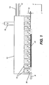
- Distribution manifold 10 for atomic layer deposition onto a substrate 20 according to the present invention.
- Distribution manifold 10 has a gas inlet port 14 for accepting a first gaseous material, a gas inlet port 16 for accepting a second gaseous material, and a gas inlet port 18 for accepting a third gaseous material. These gases are emitted at an output face 36 via output channels 12, having a structural arrangement described subsequently.
- the arrows in Figure 1 and subsequent Figures 2-3B refer to the diffusive transport of the gaseous material, and not the flow, received from an output channel. The flow is substantially directed out of the page of the figure, as described further below.
- gas inlet ports 14 and 16 are adapted to accept first and second gases that react sequentially on the substrate surface to effect ALD deposition, and gas inlet port 18 receives a purge gas that is inert with respect to the first and second gases.
- Distribution manifold 10 is spaced a distance D from substrate 20, provided on a substrate support, as described in more detail subsequently. Reciprocating motion can be provided between substrate 20 and distribution manifold 10, either by movement of substrate 20, by movement of distribution manifold 10, or by movement of both substrate 20 and distribution manifold 10. In the particular embodiment shown in Figure 1 , substrate 20 is moved across output face 36 in reciprocating fashion, as indicated by the arrow R and by phantom outlines to the right and left of substrate 20 in Figure 1 .
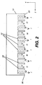
- each output channel 12 is in gaseous flow communication with one of gas inlet ports 14, 16 or 18 seen in Figure 1 .
- Each output channel 12 delivers typically a first reactant gaseous material O, or a second reactant gaseous material M, or a third inert gaseous material I.
- Figure 2 shows a relatively basic or simple arrangement of gases. It is envisioned that a plurality of non-metal deposition precursors (like material O) or a plurality of metal-containing precursor materials (like material M) may be delivered sequentially at various ports in a thin-film single deposition. Alternately, a mixture of reactant gases, for example, a mixture of metal precursor materials or a mixture of metal and non-metal precursors may be applied at a single output channel when making complex thin film materials, for example, having alternate layers of metals or having lesser amounts of dopants admixed in a metal oxide material.
- the critical requirement is that an inter-stream labeled I should separate any reactant channels in which the gases are likely to react with each other.
- First and second reactant gaseous materials O and M react with each other to effect ALD deposition, but neither reactant gaseous material O nor M reacts with inert gaseous material I.
- first reactant gaseous material O could be an oxidizing gaseous material
- second reactant gaseous material M would be a metal-containing compound, such as a material containing zinc.
- Inert gaseous material I could be nitrogen, argon, helium, or other gases commonly used as purge gases in ALD systems.
- Inert gaseous material I is inert with respect to first or second reactant gaseous materials O and M.
- Reaction between first and second reactant gaseous materials would form a metal oxide or other binary compound, such as zinc oxide ZnO or ZnS, used in semiconductors, in one embodiment. Reactions between more than two reactant gaseous materials could form a ternary compound, for example, ZnAlO.
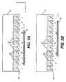
- FIG. 3A The cross-sectional views of Figures 3A and 3B show, in simplified schematic form, the ALD coating operation performed as substrate 20 passes along output face 36 of distribution manifold 10 when delivering reactant gaseous materials O and M.
- the surface of substrate 20 first receives an oxidizing material from output channels 12 designated as delivering first reactant gaseous material O.
- the surface of the substrate now contains a partially reacted form of material O, which is susceptible to reaction with material M.
- the reaction with M takes place, forming a metallic oxide or some other thin film material that can be formed from two reactant gaseous materials.
- inert gaseous material I is provided in every alternate output channel 12, between the flows of first and second reactant gaseous materials O and M.
- Sequential output channels 12 are adjacent, that is, share a common boundary, formed by partitions 22 in the embodiments shown.
- output channels 12 are defined and separated from each other by partitions 22 that extend at a perpendicular to the surface of substrate 20.
- distribution manifold 10 directs a gas flow (preferably substantially laminar in one embodiment) along the surface for each reactant and inert gas and handles spent gases and reaction by-products in a different manner, as described subsequently.
- the preferably unidirectional flow used in the present invention is directed along and generally parallel to the plane of the substrate surface. In other words, the flow of gases is substantially transverse to the plane of a substrate rather than perpendicular to the substrate being treated.
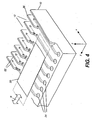
- Figures 4 and 5 show perspective views of one embodiment of distribution manifold 10 from the output face 36 (that is, from the underside with respect to Figures 1 - 3B ). Partitions 22 that define and separate the adjacent output channels 12 are represented as partially cut away, to allow better visibility for the gas flows flowing from gas outlet ports 24. Figures 4 and 5 also show reference x,y,z coordinate axis assignments used in the figures of this disclosure. Output channels 12 are substantially in parallel and extend in a length direction that corresponds to the x coordinate axis. Reciprocating motion of substrate 20, or motion relative to substrate 20, is in the y coordinate direction, using this coordinate assignment.
- Figure 5 shows the flows F I , F O , and F M for the various gaseous materials delivered from distribution manifold 10 with this embodiment.
- Flows F I , F O , and F M are in the x -direction, that is, along the length of elongated output channels 12.
- FIG. 6A The cross-sectional views of Figures 6A, 6B , 6C, and 6D are taken orthogonally to the cross-sections of Figures 1-3B and show preferably gas flows in one direction from this view.
- the corresponding gaseous material flows from a gas output port 24, shown in phantom in the views of Figures 6A, 6B , 6C, and 6D .
- a flow F1 directs the gaseous material along the length of output channel 12 and across substrate 20, as was described with reference to Figures 4 and 5 .
- Flow F1 continues past the edge of distribution manifold 10 in this arrangement, flowing outward into the environment or, if desirable, to a gas collection manifold (not shown).
- Figure 6B shows an alternative embodiment for a flow F2 in which output channel 12 also provides an exhaust port 26 for redirection or drawing off of the gas flow.
- Figure 6C shows an alternative embodiment for a flow F3, in which gas output port 24 is centrally located within output channel 12 and directs gaseous material to flow along the channel in both directions.
- Figure 6D shows an alternate embodiment for flow F4, in which gas output port 24 is also centrally positioned, with multiple exhaust ports 26 suitably placed near the extreme ends of output channel 12.
- unidirectional flows are preferred, some degree of mixing can occur and even may be beneficial to some extent, depending on the flow rates and other circumstances involved in a particular application.
- a particular distribution manifold 10 may use output channels 12 configured using any one of the flow configurations or combinations thereof, either the F1 flow of Figure 6A , the F2 flow of Figure 6B , the F3 flow of Figure 6C , the F4 flow of Figure 6D , or some other variation in which gaseous material is directed to flow across substrate 20 along output channel 12, preferably in a substantially laminar fashion.
- one or more exhaust ports 26 are provided for each output channel 12 that delivers a reactant gaseous material.
- output channels 12 for first and second reactant gaseous materials, labeled O and M are configured with exhaust ports 26 to vent or draw off the reactant substances, following the pattern of flow F2 ( Figure 6B ). This allows some recycle of materials and prevents undesirable mixing and reaction near the end of the manifold.
- Output channels 12 for inert gaseous material, labeled I do not use exhaust ports 26 and thus follow the pattern of flow F1 ( Figure 6A ).
- Exhaust port 26 is not a vacuum port, in the conventional sense, but is simply provided to draw off the flow in its corresponding output channel 12, thus facilitating a uniform flow pattern within the channel.
- a negative draw just slightly less than the opposite of the gas pressure at gas output port 24, can help to facilitate an orderly flow.
- the negative draw can, for example, operate at a pressure of between 0.9 and 1.0 atmosphere, whereas a typical vacuum is, for example, below 0.1 atmosphere.
- An optional baffle 58 as shown in dotted outline in Figures 6B and 6D , may be provided to redirect the flow pattern into exhaust port 26.
- a flow pattern such as F1 or F3, or its variants F2 and F4 with exhaust port 26, provides a number of advantages over conventional approaches, such as those noted earlier in the background section, that use an array of continuous gas sources directed orthogonally against the surface. Because separate vacuum channels are not needed, distribution manifold 10 can be very compact, directing a gaseous material along each adjacent output channel. Flow dynamics are also improved over earlier approaches, since the flow that is used is less likely to encounter barrier layer effects. Inert gas flow F I provides a type of "sweep purge" that removes excess material from the previous output channel 12 as well as unwanted reaction by-products.
- Inert gas flow F I also helps to separate the reactant gases of flows F O and F M , so that mixing of these reactant gases above the surface of substrate 20 is minimized or eliminated. Because conventional vacuum is not used, the design of distribution manifold 10 is less complex than gas array designs that require a vacuum pump channel between each gas delivery channel, with vacuum levels carefully calibrated to balance against output flows.
- the flow arrangement used in the present invention depends on the distance D, shown in Figure 1 , between substrate 20 and output face 36 of distribution manifold 10. Because no gas flow around partition 22 to a vacuum exhaust is needed, output face 36 can be positioned very closely, to within 1 mil (approximately 0.025 mm) of the substrate surface. By comparison, an earlier approach such as that described in the US Patent No. 6,821,563 to Yudovsky , cited earlier, required gas flow around the edges of channel sidewalls and was thus limited to 0.5 mm or greater distance to the substrate surface. Positioning the distribution manifold 10 closer to the substrate surface is preferred in the present invention. In a preferred embodiment, distance D from the surface of the substrate can be 0.4 mm or less, preferably within 0.3 mm, more preferably within 0.25 mm of the output face of the distribution manifold.
- FIG. 7A and 7B show why it is desirable that the distance D is relatively small, consistent with the operation of the invention.
- distribution manifold 10 is moving over substrate 20 from left to right, as the arrow indicates.
- output channel 12 carrying a reactive gaseous material M moves to the right over an area, it encounters a diffusion layer 72 from the next adjacent (previous-in-time) output channel that is primarily inert gaseous material I.
- reactive gaseous material M should diffuse through diffusion layer 72, which has a thickness proportional to distance D.
- Figure 7B shows what happens when distance D is reduced: diffusion layer 72 is reduced proportionately.
- Diffusion through diffusion layer 72 happens more quickly and more efficiently, allowing less waste and reducing the overall amount of time needed for reaction on the surface of substrate 20.
- the lower partition walls 22 also prevent less gas to remain from the previous-in time output channel gas.
- the flow of the gases in the channels are perpendicular to the page of the Figures 7A and 7B , as shown by the back of the arrow, which flow maintains a concentration gradient that aids the diffusion through the thin diffusion layer 72 to the surface of the substrate.
- the surface is exposed to the gas flow of M for sufficient time for diffusion and any mixing to replace the previous-in-time output channel gas. It is noted that since the flow of gas is across the surface rather than directly into the surface it limits the undesirable mixing of reactant gases between outlet channels, which might otherwise be exacerbated by relative oscillation of the manifold and/or substrate.
- gas output port 24 may be inclined at an angle away from normal, as indicated in Figures 6A and 6B .
- some type of gas flow redirecting structure may also be employed to redirect a downward flow from gas output port 24 so that it forms a flow that runs substantially in parallel to output face 36.
- FIG. 8 shows output face 36 of a portion of distribution manifold 10 in one embodiment.
- redirecting plates 38 are positioned in each of the output channels 12 for directing reactant gaseous materials.
- only output channels 12 that deliver reactant gaseous materials are provided with redirecting plates 38 and exhaust ports 26.
- This particular arrangement may be advantageous in some applications, where it is advantageous to surround distribution manifold 10 with inert gas, such as to reduce unwanted intake of ambient gases.
- redirecting plates 38 could be used on all output channels 12.
- exhaust ports 26 could be used on some or all output channels 12.
- redirecting plates can be used on all channels, but the outlet edge of the redirecting plate may be at a different x-axis position depending upon which channel is considered.
- Figure 8 also shows the pattern of output channels in one embodiment.
- inert gas channels I as the outermost channels of distribution manifold 10.
- Oxidation channels with first reactant gaseous material O are next to the outermost channels, since these condition the surface for ALD reaction with the metallic component of second reactant gaseous material M.
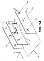
- Figure 9 shows one embodiment of a distribution manifold 10 in which the channels of width W, length L, and height H are formed from stacked metal plates 42 and 44 having apertures 40 forming ducts 46a,b,c.
- Figure l0A shows an exploded view of a single output channel 12 section of distribution manifold 10 formed in this way, showing an arrangement of apertures 40 in alternating partition plates 42 and delivery plates 44.
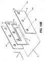
- Figure 10B shows a similar exploded view for an adjacent output channel 12.
- Ducts 46a, 46b, and 46c formed by alignment of apertures 40, extend through distribution manifold 10 and provide input conduits for gaseous flow communication, accepting the different reactant and inert gaseous materials from external sources and providing the redirecting structures that provide gas flows along output face 36 described earlier. Baffles and other redirecting structures are not shown in these figures, but could be provided using stacked plates suitably structured, or applied after the device is assembled.
- FIG. 10A The exploded views of Figures 10A and 10B each show a single output channel 12 formed from stacked plates 42 and 44.
- output channel 12 shown provides gaseous material provided from duct 46b.
- Ducts 46a and 46c conduct other gases past this channel in the embodiment shown in Figure 10A .
- Delivery plate 44 dimensioned and apertured differently than the partition plates 42 that bound output channel 12 acting as a shim and a spacer element as well as guiding the flow of gaseous material, contains a redirecting chamber 48 that redirects a portion of the gas in duct 46b into gas flow F1.
- output channel 12 shown provides gaseous material provided from duct 46a.
- Ducts 46b and 46c conduct other gases past this channel in the embodiment shown in Figure 10B .
- Plates 42 and 44 should be of a suitable metal for conducting the reactive gaseous materials, such as stainless steel or other metal for example.
- the gas flow delivered to the substrate is uniform across all of the channels delivering a particle flow (I, M, or O). This can be accomplished by proper design of the plates, such as having restrictions in some part of the flow pattern for each plate which are accurately machined to provide a reproducible pressure drop for each channel.
- the method of stacking plates is a particularly useful way of constructing the article of this invention, there are a number of other methods to build such structures and may be useful in alternate embodiments.
- the apparatus may be constructed by direct machining of a metal block, or of several metal blocks adhered together.
- molding techniques involving internal mold features can be employed, as will be understood by the skilled artisan.
- the apparatus can also be constructed using any of a number of stereolithography techniques.
- each output channel 12 can be constructed of very small size, with each output channel 12 having the width of a sheet of metal plating.
- output channel 12 is 0.034 inches (0.86 mm) in width W.
- the width of the opening of at least one elongated output channel, preferably all, is between 0.2 to 5 mm, more preferably 0.50 and 1.50 mm.
- Output channels 12 for different materials could be fabricated at different thicknesses to obtain width W ranges, preferably from 0.01 inches (0.25 mm) to 0.1 inches (2.5 mm) for a compact arrangement.
- the length L of output channel 12 can vary, depending on the needed uniformity and desired gas pressure. In one embodiment, output channel length L is 3 inches (75 mm). The height H of output channels 12 formed from extending portions of stacked plates 42 is 0.1 inches (2.5 mm) in one embodiment.
- FIG. 11 there is shown an envelopment gas flow F E by which an additional flow of inert gas is used on one or more sides of distribution manifold 10 to prevent ambient gases from contaminating the process gases.
- distribution manifold 10 requires movement relative to the surface of substrate 20 in order to perform its deposition function.
- This relative movement can be obtained in a number of ways, including movement of either or both distribution manifold 10 and substrate 20, such as by movement of an apparatus that provides a substrate support. Movement can be oscillating or reciprocating or could be continuous movement, depending on how many deposition cycles are needed. Rotation of a substrate can also be used, particularly in a batch process, although continuous processes are preferred.
- ALD atomic layer deposition
- the distance between output channels for O and M reactant gaseous materials determines the needed distance for reciprocating movement to complete each cycle.
- reciprocating motion (along the y axis as used herein) of at least 0.204 inches would be required.
- an area of substrate 20 would be exposed to both first reactant gaseous material O and second reactant gaseous material M with movement over this distance.
- consideration for uniformity may require a measure of randomness to the amount of reciprocating motion in each cycle, such as to reduce edge effects or build-up along the extremes of reciprocation travel.
- a distribution manifold 10 may have only enough output channels 12 to provide a single cycle. Alternately, distribution manifold 10 may have an arrangement of multiple cycles, enabling it to cover a larger deposition area or enabling its reciprocating motion over a distance that allows two or more deposition cycles in one traversal of the reciprocating motion distance.
- each O-M cycle formed a layer of one atomic diameter over 1 ⁇ 4 of the treated surface.
- four cycles in this case, are needed to form a uniform layer of 1 atomic diameter over the treated surface.
- 40 cycles would be required.
- FIG. 12 shows schematically how this broader area coverage can be effected, using reciprocating motion along the y axis as shown by arrow R and also movement orthogonal or transverse to the reciprocating motion, relative to the x axis.
- motion in either the x or y direction can be effected either by movement of distribution manifold 10, or by movement of substrate 20 provided with a substrate support 74 that provides movement, or by movement of both distribution manifold 10 and substrate 20.
- the relative motion of the distribution manifold and the substrate are perpendicular to each other. It is also possible to have this relative motion in parallel. In this case, the relative motion needs to have a nonzero frequency component that represents the oscillation and a zero frequency component that represents the displacement of the substrate.
- This combination can be achieved by: an oscillation combined with displacement of the distribution manifold over a fixed substrate; an oscillation combined with displacement of the substrate relative to a fixed substrate distribution manifold; or any combinations wherein the oscillation and fixed motion are provided by movements of both the distribution manifold and the substrate.
- ALD can be performed at or near atmospheric pressure and over a broad range of ambient and substrate temperatures, preferably at a temperature of under 300°C.
- a relatively clean environment is needed to minimize the likelihood of contamination; however, full "clean room” conditions or an inert gas-filled enclosure would not be required for obtaining good performance when using preferred embodiments of the apparatus of the present invention.
- Figure 13 shows an Atomic Layer Deposition (ALD) system 60 having a chamber 50 for providing a relatively well-controlled and contaminant-free environment.
- Gas supplies 28a, 28b, and 28c provide the first, second, and third gaseous materials to distribution manifold 10 through supply lines 32.
- the optional use of flexible supply lines 32 facilitates ease of movement of distribution manifold 10.
- optional vacuum vapor recovery apparatus and other support components are not shown in Figure 12 but could also be used.
- a transport subsystem 54 provides a substrate support that conveys substrate 20 along output face 36 of distribution manifold 10, providing movement in the x direction, using the coordinate axis system employed in the present disclosure.
- Motion control as well as overall control of valves and other supporting components, can be provided by a control logic processor 56, such as a computer or dedicated microprocessor assembly, for example.
- control logic processor 56 controls an actuator 30 for providing reciprocating motion to distribution manifold 10 and also controls a transport motor 52 of transport subsystem 54.
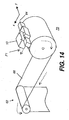
- Figure 14 shows an alternate embodiment of an Atomic Layer Deposition (ALD) system 70 for thin film deposition onto a web substrate 66 that is conveyed past distribution manifold 10 along a web conveyor 62 that acts as a substrate support.
- a distribution manifold transport 64 conveys distribution manifold 10 across the surface of web substrate 66 in a direction transverse to the web travel direction.
- distribution manifold transport 64 uses a lead screw that traverses the width of web substrate 66.
- multiple distribution manifolds 10 are used, at suitable positions along web 62.
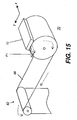
- FIG 15 shows another Atomic Layer Deposition (ALD) system 70 in a web arrangement, using a stationary distribution manifold 10 in which the flow patterns are oriented orthogonally to the configuration of Figure 13.
- ALD Atomic Layer Deposition
- motion of web conveyor 62 itself provides the movement needed for ALD deposition.
- Reciprocating motion could also be used in this environment, such as by repeatedly reversing the direction of rotation of a web roller to move substrate 66 forward and backwards relative to distribution manifold 10.
- Reciprocation motion can also be obtained by allowing a reciprocating motion of the distribution manifold across an arc whose axis coincides with the roller axis, while the web is moved in a constant motion.
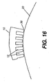
- FIG 16 an embodiment of a portion of distribution manifold 10 is shown in which output face 36 has an amount of curvature, which might be advantageous for some web coating applications. Convex or concave curvature could be provided.
- the apparatus of the present invention is advantaged in its capability to perform deposition onto a substrate over a broad range of temperatures, including room or near-room temperature in some embodiments.
- the apparatus of the present invention can operate in a vacuum environment, but is particularly well suited for operation at or near atmospheric pressure.
- the flow setup is supplied with nitrogen gas flow 81 that has been purified to remove oxygen and water contamination to below 1 ppm.
- the gas is diverted by a manifold to several flow meters which control flows of purge gases and of gases diverted through bubblers to select the reactive precursors.
- air flow 90 is also delivered to the apparatus. The air is pretreated to remove moisture.
- metal precursor flow 92 containing metal precursors diluted in nitrogen gas
- oxidizer-containing flow 93 containing non-metal precursors or oxidizers diluted in nitrogen gas
- nitrogen purge flow 95 composed only of the inert gas.
- Gas bubbler 82 contains a 1 molar solution of diethylzinc in hexanes.
- Gas bubbler 83 contains a 2 molar solution of trimethylaluminum in hexanes. Both bubblers are kept at room temperature.
- Flow meters 85 and 86 deliver flows of pure nitrogen to the diethylzinc bubbler 82 and trimethylaluminum bubbler 83, respectively.
- the output of the bubblers now contain nitrogen gas saturated with the respective precursor solutions. These output flows are mixed with a nitrogen gas dilution flow delivered from flow meter 87 to yield the overall flow of metal precursor flow 92.
- Flow meter 85 To Diethylzinc Bubbler Flow Flow meter 86: To Trimethylaluminum Bubbler Flow Flow meter 87: To Metal Precursor Dilution Flow
- Gas bubbler 84 contains pure water at room temperature.
- Flow meter 88 delivers a flow of pure nitrogen gas to gas bubbler 84, the output of which represents a stream of saturated water vapor.
- An airflow is controlled by flow meter 91.
- the water bubbler output and air streams are mixed with dilution stream from flow meter 89 to produce the overall flow of oxidizer-containing flow 93 which has a variable water composition, oxygen composition, and total flow.
- the flows will be as follows: Flow meter 88: To Water Bubbler Flow meter 89: To Oxidizer Dilution Flow Flow meter 91: To Air Flow
- Flow meter 94 controls the flow of pure nitrogen that is to be delivered to the coating apparatus.
- Streams or Flows 92, 93, and 95 are then delivered to an atmospheric pressure coating head where they are directed out of the channels or microchamber slots as indicated in Figure 18 .
- a gap 96 of approximately 0.15 mm exists between the microchambers and the substrate 97.
- the microchambers are approximately 2.5 mm tall, 0.86 mm wide, and run the length of the coating head which is 76 mm.
- the reactant materials in this configuration are delivered to the middle of the slot and flow out of the front and back.
- the coating head In order to perform a deposition, the coating head is positioned over a portion of the substrate and then moved in a reciprocating fashion over the substrate, as represented by the arrow 98.
- the length of the reciprocation cycle was 32mm.
- the rate if motion of the reciprocation cycle is 30 mm/sec.
- Transistor characterization of the fabricated devices fabricated using the present invention was performed with a Hewlett Packard HP 4156® parameter analyzer. Device testing was done in air in a dark enclosure.
- the drain current (Id) was measured as a function of source-drain voltage (Vd) for various values of gate voltage (Vg). Furthermore, for each device the drain current was measured as a function of gate voltage for various values of source-drain voltage. For most devices, Vg was swept from -10 V to 40 V for each of the drain voltages measured, typically 10 V, 20 V, and 30 V. Mobility measurements were taken from the 30 V sweep.
- Parameters extracted from the data include field-effect mobility ( ⁇ ), threshold voltage (Vth), and the ratio of Ion/Ioff for the measured drain current.
- the field-effect mobility was extracted in the saturation region, where Vd > Vg - Vth.
- the saturation field-effect mobility was extracted from a straight-line fit to the linear portion of the ⁇ I d versus Vg curve.
- the threshold voltage, V th is the x-intercept of this straight-line fit.
- the log of the drain current as a function of gate voltage was plotted. Parameters extracted from the log I d plot include the I on /I off ratio.
- the I on /I off ratio is simply the ratio of the maximum to minimum drain current.
- Breakdown voltage characterization of the fabricated devices was performed with a HEWLETT PACKARD HP 4156 parameter analyzer. Device testing was done in air in a dark enclosure.
- the breakdown voltage corresponds to the voltage placed across the layer at which a substantial current begins to flow due to dielectric breakdown.
- the dielectric film in question was coated on a conductor (typically a heavily doped silicon wafer) and a metal contact was placed on top of the dielectric layer.
- the silicon wafer was held at ground, while the voltage applied to the top metal contact was swept from 0 to 100 V. During the sweep the current flowing into the top metal contact was measured. Although significant current leakage can occur prior to breakdown, the breakdown voltage is taken as a point at which a sharp rise in current flow can be seen.
- Thickness of the aluminum oxide films of the following examples were measured using a J. A. WOOLAM ALPHA-SE white light ellipsometer. The data acquired were fit to a model in which the layer under examination was represented by a Cauchy dispersion model. The output of the model fitting yields the film thickness and refractive index.
- This example shows the production of a zinc oxide semiconductor film according to the present invention used to produce a working thin film transistor.
- the gate of the device is a heavily doped silicon wafer
- the insulator is a film of silicon dioxide grown by a thermal process on the silicon wafer prior to deposition of the zinc oxide semiconducting film.
- the zinc oxide semiconductor layer was applied using the inventive deposition system. Two runs were made with the substrate temperature at 200°C and the following conditions: TABLE 1 Sample Diethylzinc Bubbler Blow (sccm) Metal Precursor Dilution Flow (sccm) Air Flow (sccm) Water Bubbler Flow (sccm) Oxidizer Dilution Flow (sccm) Nitrogen Purge Flow (sccm) Cycles 1-A 10 620 5 10 1000 1500 40 1-B 5 620 5 5 1000 1500 40
- This example shows the production of aluminum oxide films according to the present invention, demonstrating the capability to make high quality insulating films with good breakdown voltage.
- a bare silicon wafer is used as one electrode on which is grown a film of aluminum oxide using the inventive equipment described above.
- This example shows the production of a working transistor device using heavily doped silicon as the gate material but then employing Al 2 O 3 as the dielectric and ZnO as the semiconductor, in which both of the latter materials are deposited using the present invention.
- the aluminum oxide films were deposited first according to following conditions: TABLE 5 Sample Trimethyl-Aluminum Bubbler Flow (sccm) Metal Precursor Dilution Flow (sccm) Air Flow (sccm) Water Bubbler Flow (sccm) Oxidizer Dilution Flow (sccm) Nitrogen Purge Flow (sccm) Cycles 3-A 25 620 10 20 1100 1500 80 3-B 25 620 10 20 1100 1500 60
- This example shows the production of a working transistor device using heavily doped silicon as the gate material but then employing Al 2 O 3 as the dielectric and ZnO as the semiconductor in which both of the latter materials are deposited according to the present invention, with variations in deposition temperature to demonstrate the capability to produce useful devices over a range of temperatures.
- This example shows the production of an aluminum oxide film on a glass substrate, demonstrating that a variety of substrates can be used in this invention.
- the aluminum oxide films were deposited first according to following conditions: TABLE 11 Trimethyl-Alum. Bubbler Flow (sccm) Metal Precursor Dilution Flow (sccm) Air Flow (sccm) Water Bubbler Flow (sccm) Oxidizer Dilution Flow (sccm) Nitrogen Purge Flow (sccm) Cycles 5 620 10 25 1100 1500 175
- This example shows the production of a working transistor device using indium tin oxide as the gate material but then employing Al 2 O 3 as the dielectric and ZnO as the semiconductor, wherein both of the latter materials are deposited using the invention described in this patent.
- the aluminum oxide films were deposited first according to following conditions: TABLE 13 Trimethyl-Aluminum Bubbler flow (sccm) Metal Precursor Dilution Flow (sccm) Air Flow (sccm) Water Bubbler Flow (sccm) Oxidizer Dilution Flow (sccm) Nitrogen Purge Flow (sccm) Cycles Temp. (C) 16 620 10 25 1100 1500 175 200C
- the samples were given various cleaning treatments as listed in the table below.
- the sonication in isopropyl alcohol (IPA) was done with a bench top ultrasonic cleaner, and consisted of sonication of the sample in IPA for 5 minutes.
- the O 2 Plasma/CFx treatment consisted of a 2' 02 plasma treatment as described in Example 5 above, followed by deposition of a 1 nm fluorocarbon (CFx) layer by plasma-assisted deposition of CHF 3 as described in US 6,208,075 .
- TABLE 15 Sample Substrate Preparation Mobility Vth 6-A Sonication in IPA 1.2 3.8 6-B O 2 Plasma / CFx 2.8 3.8
- This example shows the capability to produce a conductive material according to the present invention.
- the conductor is an aluminum doped zinc oxide.
- the films were grown by simultaneous addition of diethylzinc and trimethylaluminum as shown in the table below: TABLE 16 Sample Diethylzinc Bubbler Flow (sccm) Trimethyl Aluminum Bubbler Flow (sccm) Metal Precursor Dilution Flow (sccm) Air Flow (sccm) Water Bubbler Flow (sccm) Oxidizer Dilution Flow (sccm) Nitrogen Purge Flow (sccm) Cycles Temp (C) 3 30 2 620 10 15 1100 1500 300 350 6 30 2 620 10 15 1100 1500 300 200
Landscapes
- Chemical & Material Sciences (AREA)
- General Chemical & Material Sciences (AREA)
- Chemical Kinetics & Catalysis (AREA)
- Engineering & Computer Science (AREA)
- Materials Engineering (AREA)
- Mechanical Engineering (AREA)
- Metallurgy (AREA)
- Organic Chemistry (AREA)
- Chemical Vapour Deposition (AREA)
- Physical Vapour Deposition (AREA)
Applications Claiming Priority (2)
| Application Number | Priority Date | Filing Date | Title |
|---|---|---|---|
| US11/392,006 US7456429B2 (en) | 2006-03-29 | 2006-03-29 | Apparatus for atomic layer deposition |
| PCT/US2007/006390 WO2007126582A2 (en) | 2006-03-29 | 2007-03-14 | Apparatus for atomic layer deposition |
Publications (2)
| Publication Number | Publication Date |
|---|---|
| EP1999296A2 EP1999296A2 (en) | 2008-12-10 |
| EP1999296B1 true EP1999296B1 (en) | 2012-01-25 |
Family
ID=38544360
Family Applications (1)
| Application Number | Title | Priority Date | Filing Date |
|---|---|---|---|
| EP07753045A Active EP1999296B1 (en) | 2006-03-29 | 2007-03-14 | Apparatus for atomic layer deposition |
Country Status (7)
| Country | Link |
|---|---|
| US (1) | US7456429B2 (enExample) |
| EP (1) | EP1999296B1 (enExample) |
| JP (1) | JP2009531548A (enExample) |
| KR (1) | KR20080106563A (enExample) |
| CN (1) | CN101415862A (enExample) |
| TW (1) | TWI396769B (enExample) |
| WO (1) | WO2007126582A2 (enExample) |
Cited By (1)
| Publication number | Priority date | Publication date | Assignee | Title |
|---|---|---|---|---|
| DE102012111484A1 (de) * | 2012-11-27 | 2014-05-28 | Aixtron Se | Vorrichtung und Verfahren zum Bearbeiten streifenförmiger Substrate |
Families Citing this family (453)
| Publication number | Priority date | Publication date | Assignee | Title |
|---|---|---|---|---|
| JP2006253696A (ja) * | 2005-03-10 | 2006-09-21 | Asm America Inc | ガスインジェクタ制御システム |
| BRPI0709199A2 (pt) | 2006-03-26 | 2011-06-28 | Lotus Applied Technology Llc | sistema e método para depositar uma pelìcula fina em um substrato flexìvel |
| US20070281089A1 (en) * | 2006-06-05 | 2007-12-06 | General Electric Company | Systems and methods for roll-to-roll atomic layer deposition on continuously fed objects |
| US7615486B2 (en) * | 2007-04-17 | 2009-11-10 | Lam Research Corporation | Apparatus and method for integrated surface treatment and deposition for copper interconnect |
| US7573420B2 (en) * | 2007-05-14 | 2009-08-11 | Infineon Technologies Ag | RF front-end for a radar system |
| US20080166880A1 (en) * | 2007-01-08 | 2008-07-10 | Levy David H | Delivery device for deposition |
| US11136667B2 (en) | 2007-01-08 | 2021-10-05 | Eastman Kodak Company | Deposition system and method using a delivery head separated from a substrate by gas pressure |
| US7789961B2 (en) * | 2007-01-08 | 2010-09-07 | Eastman Kodak Company | Delivery device comprising gas diffuser for thin film deposition |
| US8207063B2 (en) * | 2007-01-26 | 2012-06-26 | Eastman Kodak Company | Process for atomic layer deposition |
| US20080299771A1 (en) * | 2007-06-04 | 2008-12-04 | Irving Lyn M | Methods of making thin film transistors comprising zinc-oxide-based semiconductor materials and transistors made thereby |
| US7572686B2 (en) * | 2007-09-26 | 2009-08-11 | Eastman Kodak Company | System for thin film deposition utilizing compensating forces |
| US8211231B2 (en) * | 2007-09-26 | 2012-07-03 | Eastman Kodak Company | Delivery device for deposition |
| US7858144B2 (en) * | 2007-09-26 | 2010-12-28 | Eastman Kodak Company | Process for depositing organic materials |
| US8182608B2 (en) * | 2007-09-26 | 2012-05-22 | Eastman Kodak Company | Deposition system for thin film formation |
| US8398770B2 (en) * | 2007-09-26 | 2013-03-19 | Eastman Kodak Company | Deposition system for thin film formation |
| JP5179389B2 (ja) * | 2008-03-19 | 2013-04-10 | 東京エレクトロン株式会社 | シャワーヘッド及び基板処理装置 |
| US20090291209A1 (en) * | 2008-05-20 | 2009-11-26 | Asm International N.V. | Apparatus and method for high-throughput atomic layer deposition |
| US9238867B2 (en) * | 2008-05-20 | 2016-01-19 | Asm International N.V. | Apparatus and method for high-throughput atomic layer deposition |
| KR20090122727A (ko) * | 2008-05-26 | 2009-12-01 | 삼성전자주식회사 | 원자층 증착 장치와 이를 이용한 원자층 증착 방법 |
| KR101639230B1 (ko) * | 2008-12-04 | 2016-07-13 | 비코 인스트루먼츠 인코포레이티드 | 화학 기상 증착 유동물 유입구 부재 및 방법 |
| JP4523661B1 (ja) * | 2009-03-10 | 2010-08-11 | 三井造船株式会社 | 原子層堆積装置及び薄膜形成方法 |
| US9394608B2 (en) | 2009-04-06 | 2016-07-19 | Asm America, Inc. | Semiconductor processing reactor and components thereof |
| US8657959B2 (en) * | 2009-07-31 | 2014-02-25 | E I Du Pont De Nemours And Company | Apparatus for atomic layer deposition on a moving substrate |
| US20110023775A1 (en) * | 2009-07-31 | 2011-02-03 | E.I. Du Pont De Nemours And Company | Apparatus for atomic layer deposition |
| US8802201B2 (en) | 2009-08-14 | 2014-08-12 | Asm America, Inc. | Systems and methods for thin-film deposition of metal oxides using excited nitrogen-oxygen species |
| WO2011047210A2 (en) * | 2009-10-14 | 2011-04-21 | Lotus Applied Technology, Llc | Inhibiting excess precursor transport between separate precursor zones in an atomic layer deposition system |
| US20110097494A1 (en) | 2009-10-27 | 2011-04-28 | Kerr Roger S | Fluid conveyance system including flexible retaining mechanism |
| US20110097491A1 (en) | 2009-10-27 | 2011-04-28 | Levy David H | Conveyance system including opposed fluid distribution manifolds |
| US20110097489A1 (en) * | 2009-10-27 | 2011-04-28 | Kerr Roger S | Distribution manifold including multiple fluid communication ports |
| US20110097488A1 (en) * | 2009-10-27 | 2011-04-28 | Kerr Roger S | Fluid distribution manifold including mirrored finish plate |
| US20110097492A1 (en) * | 2009-10-27 | 2011-04-28 | Kerr Roger S | Fluid distribution manifold operating state management system |
| US20110097487A1 (en) | 2009-10-27 | 2011-04-28 | Kerr Roger S | Fluid distribution manifold including bonded plates |
| US20110097490A1 (en) * | 2009-10-27 | 2011-04-28 | Kerr Roger S | Fluid distribution manifold including compliant plates |
| US20110097493A1 (en) | 2009-10-27 | 2011-04-28 | Kerr Roger S | Fluid distribution manifold including non-parallel non-perpendicular slots |
| NL2003836C2 (en) * | 2009-11-19 | 2011-05-23 | Levitech B V | Floating wafer track with lateral stabilization mechanism. |
| US20110120544A1 (en) | 2009-11-20 | 2011-05-26 | Levy David H | Deposition inhibitor composition and method of use |
| WO2011062779A1 (en) | 2009-11-20 | 2011-05-26 | Eastman Kodak Company | Method for selective deposition and devices |
| US8637123B2 (en) | 2009-12-29 | 2014-01-28 | Lotus Applied Technology, Llc | Oxygen radical generation for radical-enhanced thin film deposition |
| EP2360293A1 (en) | 2010-02-11 | 2011-08-24 | Nederlandse Organisatie voor toegepast -natuurwetenschappelijk onderzoek TNO | Method and apparatus for depositing atomic layers on a substrate |
| US8803203B2 (en) | 2010-02-26 | 2014-08-12 | Eastman Kodak Company | Transistor including reentrant profile |
| US7923313B1 (en) | 2010-02-26 | 2011-04-12 | Eastman Kodak Company | Method of making transistor including reentrant profile |
| EP2362411A1 (en) | 2010-02-26 | 2011-08-31 | Nederlandse Organisatie voor toegepast -natuurwetenschappelijk onderzoek TNO | Apparatus and method for reactive ion etching |
| US8865259B2 (en) | 2010-04-26 | 2014-10-21 | Singulus Mocvd Gmbh I.Gr. | Method and system for inline chemical vapor deposition |
| KR101791033B1 (ko) | 2010-07-23 | 2017-10-27 | 로터스 어플라이드 테크놀로지, 엘엘씨 | 롤-투-롤 박막 증착을 위한 유연한 웹 기재의 한쪽 측면과 접촉하는 기재 이동 메커니즘 |
| US8486192B2 (en) | 2010-09-30 | 2013-07-16 | Soitec | Thermalizing gas injectors for generating increased precursor gas, material deposition systems including such injectors, and related methods |
| US8133806B1 (en) | 2010-09-30 | 2012-03-13 | S.O.I.Tec Silicon On Insulator Technologies | Systems and methods for forming semiconductor materials by atomic layer deposition |
| JP5927679B2 (ja) | 2010-10-16 | 2016-06-01 | ウルトラテック,インコーポレイテッド | Aldコーティングシステム |
| US8492769B2 (en) | 2011-01-07 | 2013-07-23 | Eastman Kodak Company | Transistor including multi-layer reentrant profile |
| US8847232B2 (en) | 2011-01-07 | 2014-09-30 | Eastman Kodak Company | Transistor including reduced channel length |
| US8409937B2 (en) | 2011-01-07 | 2013-04-02 | Eastman Kodak Company | Producing transistor including multi-layer reentrant profile |
| US8383469B2 (en) | 2011-01-07 | 2013-02-26 | Eastman Kodak Company | Producing transistor including reduced channel length |
| WO2012094357A2 (en) | 2011-01-07 | 2012-07-12 | Eastman Kodak Company | Transistor including multiple reentrant profiles |
| US7985684B1 (en) | 2011-01-07 | 2011-07-26 | Eastman Kodak Company | Actuating transistor including reduced channel length |
| US8338291B2 (en) | 2011-01-07 | 2012-12-25 | Eastman Kodak Company | Producing transistor including multiple reentrant profiles |
| WO2012094109A1 (en) | 2011-01-07 | 2012-07-12 | Eastman Kodak Company | Transistor including reduced channel length |
| US8847226B2 (en) | 2011-01-07 | 2014-09-30 | Eastman Kodak Company | Transistor including multiple reentrant profiles |
| US8304347B2 (en) | 2011-01-07 | 2012-11-06 | Eastman Kodak Company | Actuating transistor including multiple reentrant profiles |
| US20120222620A1 (en) | 2011-03-01 | 2012-09-06 | Applied Materials, Inc. | Atomic Layer Deposition Carousel with Continuous Rotation and Methods of Use |
| US20120225191A1 (en) * | 2011-03-01 | 2012-09-06 | Applied Materials, Inc. | Apparatus and Process for Atomic Layer Deposition |
| US20120225204A1 (en) * | 2011-03-01 | 2012-09-06 | Applied Materials, Inc. | Apparatus and Process for Atomic Layer Deposition |
| US9312155B2 (en) | 2011-06-06 | 2016-04-12 | Asm Japan K.K. | High-throughput semiconductor-processing apparatus equipped with multiple dual-chamber modules |
| DE102011077833A1 (de) * | 2011-06-20 | 2012-12-20 | Gebr. Schmid Gmbh | Verfahren zur Bearbeitung von Substraten und Vorrichtung dazu |
| US10854498B2 (en) | 2011-07-15 | 2020-12-01 | Asm Ip Holding B.V. | Wafer-supporting device and method for producing same |
| US20130023129A1 (en) | 2011-07-20 | 2013-01-24 | Asm America, Inc. | Pressure transmitter for a semiconductor processing environment |
| US8637355B2 (en) | 2011-08-26 | 2014-01-28 | Eastman Kodak Company | Actuating transistor including single layer reentrant profile |
| US8592909B2 (en) | 2011-08-26 | 2013-11-26 | Eastman Kodak Company | Transistor including single layer reentrant profile |
| US8617942B2 (en) | 2011-08-26 | 2013-12-31 | Eastman Kodak Company | Producing transistor including single layer reentrant profile |
| US8803227B2 (en) | 2011-09-29 | 2014-08-12 | Eastman Kodak Company | Vertical transistor having reduced parasitic capacitance |
| US8865576B2 (en) | 2011-09-29 | 2014-10-21 | Eastman Kodak Company | Producing vertical transistor having reduced parasitic capacitance |
| US8273654B1 (en) | 2011-09-29 | 2012-09-25 | Eastman Kodak Company | Producing a vertical transistor including reentrant profile |
| US8623757B2 (en) | 2011-09-29 | 2014-01-07 | Eastmak Kodak Company | Producing a vertical transistor including reentrant profile |
| US9017481B1 (en) | 2011-10-28 | 2015-04-28 | Asm America, Inc. | Process feed management for semiconductor substrate processing |
| CN102424958A (zh) * | 2011-11-17 | 2012-04-25 | 陈聪茂 | 用于连续制造金属薄膜太阳能电池的淀积设备及方法 |
| US20130143415A1 (en) * | 2011-12-01 | 2013-06-06 | Applied Materials, Inc. | Multi-Component Film Deposition |
| US8618003B2 (en) | 2011-12-05 | 2013-12-31 | Eastman Kodak Company | Method of making electronic devices using selective deposition |
| US9748125B2 (en) | 2012-01-31 | 2017-08-29 | Applied Materials, Inc. | Continuous substrate processing system |
| US8633068B2 (en) | 2012-02-22 | 2014-01-21 | Eastman Kodak Company | Vertical transistor actuation |
| US8698230B2 (en) | 2012-02-22 | 2014-04-15 | Eastman Kodak Company | Circuit including vertical transistors with a conductive stack having reentrant profile |
| EP2860280A4 (en) | 2012-05-31 | 2016-03-23 | Toppan Printing Co Ltd | DEVICE FOR FORMING A ROLLED FILM |
| KR101435100B1 (ko) * | 2012-06-20 | 2014-08-29 | 주식회사 엠티에스나노테크 | 원자층 증착 장치 |
| US8846545B2 (en) | 2012-08-31 | 2014-09-30 | Eastman Kodak Company | Method of forming patterned thin film dielectric stack |
| US8653516B1 (en) | 2012-08-31 | 2014-02-18 | Eastman Kodak Company | High performance thin film transistor |
| US8791023B2 (en) | 2012-08-31 | 2014-07-29 | Eastman Kodak Company | Patterned thin film dielectric layer formation |
| US8927434B2 (en) | 2012-08-31 | 2015-01-06 | Eastman Kodak Company | Patterned thin film dielectric stack formation |
| US10714315B2 (en) | 2012-10-12 | 2020-07-14 | Asm Ip Holdings B.V. | Semiconductor reaction chamber showerhead |
| US9175389B2 (en) * | 2012-12-21 | 2015-11-03 | Intermolecular, Inc. | ALD process window combinatorial screening tool |
| US20140206137A1 (en) * | 2013-01-23 | 2014-07-24 | David H. Levy | Deposition system for thin film formation |
| US20160376700A1 (en) | 2013-02-01 | 2016-12-29 | Asm Ip Holding B.V. | System for treatment of deposition reactor |
| KR102193652B1 (ko) | 2013-03-11 | 2020-12-21 | 어플라이드 머티어리얼스, 인코포레이티드 | 고온 공정 챔버 리드 |
| CN106486601A (zh) | 2013-04-30 | 2017-03-08 | 成均馆大学校产学协力团 | 多层封装薄膜 |
| US20140374806A1 (en) | 2013-06-19 | 2014-12-25 | Lee W. Tutt | Four terminal transistor |
| US8946070B2 (en) | 2013-06-19 | 2015-02-03 | Eastman Kodak Company | Four terminal transistor fabrication |
| US8937016B2 (en) | 2013-06-21 | 2015-01-20 | Eastman Kodak Company | Substrate preparation for selective area deposition |
| US8921236B1 (en) | 2013-06-21 | 2014-12-30 | Eastman Kodak Company | Patterning for selective area deposition |
| US10683571B2 (en) | 2014-02-25 | 2020-06-16 | Asm Ip Holding B.V. | Gas supply manifold and method of supplying gases to chamber using same |
| US9147770B1 (en) | 2014-03-06 | 2015-09-29 | Eastman Kodak Company | VTFT with extended electrode |
| US9331205B2 (en) | 2014-03-06 | 2016-05-03 | Eastman Kodak Company | VTFT with post, cap, and aligned gate |
| US9153698B2 (en) | 2014-03-06 | 2015-10-06 | Eastman Kodak Company | VTFT with gate aligned to vertical structure |
| US9093470B1 (en) | 2014-03-06 | 2015-07-28 | Eastman Kodak Company | VTFT formation using capillary action |
| US9129993B1 (en) | 2014-03-06 | 2015-09-08 | Eastman Kodak Company | Forming a VTFT using printing |
| EP3114710A1 (en) | 2014-03-06 | 2017-01-11 | Eastman Kodak Company | Vtft with polymer core |
| US9178029B2 (en) | 2014-03-06 | 2015-11-03 | Eastman Kodak Company | Forming a VTFT gate using printing |
| US9236486B2 (en) | 2014-03-06 | 2016-01-12 | Eastman Kodak Company | Offset independently operable VTFT electrodes |
| US9214560B2 (en) | 2014-03-06 | 2015-12-15 | Eastman Kodak Company | VTFT including overlapping electrodes |
| US9153445B2 (en) | 2014-03-06 | 2015-10-06 | Eastman Kodak Company | Forming a VTFT with aligned gate |
| US9142647B1 (en) | 2014-03-06 | 2015-09-22 | Eastman Kodak Company | VTFT formation using selective area deposition |
| US9202898B2 (en) | 2014-03-06 | 2015-12-01 | Eastman Kodak Company | Fabricating VTFT with polymer core |
| US9117914B1 (en) | 2014-03-06 | 2015-08-25 | Eastman Kodak Company | VTFT with polymer core |
| US9123815B1 (en) | 2014-03-06 | 2015-09-01 | Eastman Kodak Company | VTFTs including offset electrodes |
| US9198283B2 (en) | 2014-03-06 | 2015-11-24 | Eastman Kodak Company | Vertically spaced electrode structure |
| US10167557B2 (en) | 2014-03-18 | 2019-01-01 | Asm Ip Holding B.V. | Gas distribution system, reactor including the system, and methods of using the same |
| US11015245B2 (en) | 2014-03-19 | 2021-05-25 | Asm Ip Holding B.V. | Gas-phase reactor and system having exhaust plenum and components thereof |
| EP2960059B1 (en) | 2014-06-25 | 2018-10-24 | Universal Display Corporation | Systems and methods of modulating flow during vapor jet deposition of organic materials |
| US11220737B2 (en) * | 2014-06-25 | 2022-01-11 | Universal Display Corporation | Systems and methods of modulating flow during vapor jet deposition of organic materials |
| US11267012B2 (en) * | 2014-06-25 | 2022-03-08 | Universal Display Corporation | Spatial control of vapor condensation using convection |
| US10858737B2 (en) | 2014-07-28 | 2020-12-08 | Asm Ip Holding B.V. | Showerhead assembly and components thereof |
| US9890456B2 (en) | 2014-08-21 | 2018-02-13 | Asm Ip Holding B.V. | Method and system for in situ formation of gas-phase compounds |
| US9620501B1 (en) | 2014-09-16 | 2017-04-11 | Eastman Kodak Company | Enhancement-depletion mode circuit element with differential passivation |
| US9443887B1 (en) | 2015-06-12 | 2016-09-13 | Eastman Kodak Company | Vertical and planar TFTS on common substrate |
| US9368491B2 (en) | 2014-10-29 | 2016-06-14 | Eastman Kodak Company | Enhancement mode inverter with variable thickness dielectric stack |
| US9634145B2 (en) | 2014-10-29 | 2017-04-25 | Eastman Kodak Company | TFT substrate with variable dielectric thickness |
| US9368490B2 (en) | 2014-10-29 | 2016-06-14 | Eastman Kodak Company | Enhancement-depletion mode inverter with two transistor architectures |
| US10941490B2 (en) | 2014-10-07 | 2021-03-09 | Asm Ip Holding B.V. | Multiple temperature range susceptor, assembly, reactor and system including the susceptor, and methods of using the same |
| US9657845B2 (en) | 2014-10-07 | 2017-05-23 | Asm Ip Holding B.V. | Variable conductance gas distribution apparatus and method |
| CN104451597B (zh) * | 2014-11-19 | 2017-08-11 | 上海纳米技术及应用国家工程研究中心有限公司 | 一种固体润滑ZnS薄膜的制备方法 |
| US10276355B2 (en) | 2015-03-12 | 2019-04-30 | Asm Ip Holding B.V. | Multi-zone reactor, system including the reactor, and method of using the same |
| US10954597B2 (en) | 2015-03-17 | 2021-03-23 | Asm Ip Holding B.V. | Atomic layer deposition apparatus |
| US9401430B1 (en) | 2015-06-12 | 2016-07-26 | Eastman Kodak Company | VTFT with a top-gate structure |
| US9653493B2 (en) | 2015-06-12 | 2017-05-16 | Eastman Kodak Company | Bottom-gate and top-gate VTFTs on common structure |
| US10458018B2 (en) | 2015-06-26 | 2019-10-29 | Asm Ip Holding B.V. | Structures including metal carbide material, devices including the structures, and methods of forming same |
| US10600673B2 (en) | 2015-07-07 | 2020-03-24 | Asm Ip Holding B.V. | Magnetic susceptor to baseplate seal |
| US10566534B2 (en) | 2015-10-12 | 2020-02-18 | Universal Display Corporation | Apparatus and method to deliver organic material via organic vapor-jet printing (OVJP) |
| US10211308B2 (en) | 2015-10-21 | 2019-02-19 | Asm Ip Holding B.V. | NbMC layers |
| US11139308B2 (en) | 2015-12-29 | 2021-10-05 | Asm Ip Holding B.V. | Atomic layer deposition of III-V compounds to form V-NAND devices |
| US10529554B2 (en) | 2016-02-19 | 2020-01-07 | Asm Ip Holding B.V. | Method for forming silicon nitride film selectively on sidewalls or flat surfaces of trenches |
| US10343920B2 (en) | 2016-03-18 | 2019-07-09 | Asm Ip Holding B.V. | Aligned carbon nanotubes |
| US10865475B2 (en) | 2016-04-21 | 2020-12-15 | Asm Ip Holding B.V. | Deposition of metal borides and silicides |
| US10190213B2 (en) | 2016-04-21 | 2019-01-29 | Asm Ip Holding B.V. | Deposition of metal borides |
| US10032628B2 (en) | 2016-05-02 | 2018-07-24 | Asm Ip Holding B.V. | Source/drain performance through conformal solid state doping |
| US10367080B2 (en) | 2016-05-02 | 2019-07-30 | Asm Ip Holding B.V. | Method of forming a germanium oxynitride film |
| US11453943B2 (en) | 2016-05-25 | 2022-09-27 | Asm Ip Holding B.V. | Method for forming carbon-containing silicon/metal oxide or nitride film by ALD using silicon precursor and hydrocarbon precursor |
| US10612137B2 (en) | 2016-07-08 | 2020-04-07 | Asm Ip Holdings B.V. | Organic reactants for atomic layer deposition |
| US9859151B1 (en) | 2016-07-08 | 2018-01-02 | Asm Ip Holding B.V. | Selective film deposition method to form air gaps |
| US10714385B2 (en) | 2016-07-19 | 2020-07-14 | Asm Ip Holding B.V. | Selective deposition of tungsten |
| KR102532607B1 (ko) | 2016-07-28 | 2023-05-15 | 에이에스엠 아이피 홀딩 비.브이. | 기판 가공 장치 및 그 동작 방법 |
| US9887082B1 (en) | 2016-07-28 | 2018-02-06 | Asm Ip Holding B.V. | Method and apparatus for filling a gap |
| US9812320B1 (en) | 2016-07-28 | 2017-11-07 | Asm Ip Holding B.V. | Method and apparatus for filling a gap |
| US9859308B1 (en) | 2016-07-29 | 2018-01-02 | Eastman Kodak Company | Multiple TFTs on common vertical support element |
| KR102613349B1 (ko) * | 2016-08-25 | 2023-12-14 | 에이에스엠 아이피 홀딩 비.브이. | 배기 장치 및 이를 이용한 기판 가공 장치와 박막 제조 방법 |
| US10643826B2 (en) | 2016-10-26 | 2020-05-05 | Asm Ip Holdings B.V. | Methods for thermally calibrating reaction chambers |
| US11532757B2 (en) | 2016-10-27 | 2022-12-20 | Asm Ip Holding B.V. | Deposition of charge trapping layers |
| US9799752B1 (en) | 2016-10-31 | 2017-10-24 | Eastman Kodak Company | Method for forming a thin-film transistor |
| US10714350B2 (en) | 2016-11-01 | 2020-07-14 | ASM IP Holdings, B.V. | Methods for forming a transition metal niobium nitride film on a substrate by atomic layer deposition and related semiconductor device structures |
| US10643904B2 (en) | 2016-11-01 | 2020-05-05 | Asm Ip Holdings B.V. | Methods for forming a semiconductor device and related semiconductor device structures |
| US10229833B2 (en) | 2016-11-01 | 2019-03-12 | Asm Ip Holding B.V. | Methods for forming a transition metal nitride film on a substrate by atomic layer deposition and related semiconductor device structures |
| US10134757B2 (en) | 2016-11-07 | 2018-11-20 | Asm Ip Holding B.V. | Method of processing a substrate and a device manufactured by using the method |
| KR102546317B1 (ko) | 2016-11-15 | 2023-06-21 | 에이에스엠 아이피 홀딩 비.브이. | 기체 공급 유닛 및 이를 포함하는 기판 처리 장치 |
| KR102762543B1 (ko) | 2016-12-14 | 2025-02-05 | 에이에스엠 아이피 홀딩 비.브이. | 기판 처리 장치 |
| US11447861B2 (en) | 2016-12-15 | 2022-09-20 | Asm Ip Holding B.V. | Sequential infiltration synthesis apparatus and a method of forming a patterned structure |
| US11581186B2 (en) | 2016-12-15 | 2023-02-14 | Asm Ip Holding B.V. | Sequential infiltration synthesis apparatus |
| KR102700194B1 (ko) | 2016-12-19 | 2024-08-28 | 에이에스엠 아이피 홀딩 비.브이. | 기판 처리 장치 |
| US10269558B2 (en) | 2016-12-22 | 2019-04-23 | Asm Ip Holding B.V. | Method of forming a structure on a substrate |
| US10867788B2 (en) | 2016-12-28 | 2020-12-15 | Asm Ip Holding B.V. | Method of forming a structure on a substrate |
| US11390950B2 (en) | 2017-01-10 | 2022-07-19 | Asm Ip Holding B.V. | Reactor system and method to reduce residue buildup during a film deposition process |
| US10655221B2 (en) | 2017-02-09 | 2020-05-19 | Asm Ip Holding B.V. | Method for depositing oxide film by thermal ALD and PEALD |
| US10468261B2 (en) | 2017-02-15 | 2019-11-05 | Asm Ip Holding B.V. | Methods for forming a metallic film on a substrate by cyclical deposition and related semiconductor device structures |
| US11248292B2 (en) | 2017-03-14 | 2022-02-15 | Eastman Kodak Company | Deposition system with moveable-position web guides |
| US10895011B2 (en) | 2017-03-14 | 2021-01-19 | Eastman Kodak Company | Modular thin film deposition system |
| US10422038B2 (en) | 2017-03-14 | 2019-09-24 | Eastman Kodak Company | Dual gas bearing substrate positioning system |
| US10584413B2 (en) | 2017-03-14 | 2020-03-10 | Eastman Kodak Company | Vertical system with vacuum pre-loaded deposition head |
| US10550476B2 (en) | 2017-03-14 | 2020-02-04 | Eastman Kodak Company | Heated gas-bearing backer |
| US10400332B2 (en) | 2017-03-14 | 2019-09-03 | Eastman Kodak Company | Deposition system with interlocking deposition heads |
| US10435788B2 (en) | 2017-03-14 | 2019-10-08 | Eastman Kodak | Deposition system with repeating motion profile |
| US20180265977A1 (en) | 2017-03-14 | 2018-09-20 | Eastman Kodak Company | Deposition system with vacuum pre-loaded deposition head |
| US10501848B2 (en) | 2017-03-14 | 2019-12-10 | Eastman Kodak Company | Deposition system with modular deposition heads |
| JP6640781B2 (ja) * | 2017-03-23 | 2020-02-05 | キオクシア株式会社 | 半導体製造装置 |
| US10529563B2 (en) | 2017-03-29 | 2020-01-07 | Asm Ip Holdings B.V. | Method for forming doped metal oxide films on a substrate by cyclical deposition and related semiconductor device structures |
| USD876504S1 (en) | 2017-04-03 | 2020-02-25 | Asm Ip Holding B.V. | Exhaust flow control ring for semiconductor deposition apparatus |
| KR102457289B1 (ko) | 2017-04-25 | 2022-10-21 | 에이에스엠 아이피 홀딩 비.브이. | 박막 증착 방법 및 반도체 장치의 제조 방법 |
| US10770286B2 (en) | 2017-05-08 | 2020-09-08 | Asm Ip Holdings B.V. | Methods for selectively forming a silicon nitride film on a substrate and related semiconductor device structures |
| US10892156B2 (en) | 2017-05-08 | 2021-01-12 | Asm Ip Holding B.V. | Methods for forming a silicon nitride film on a substrate and related semiconductor device structures |
| US12040200B2 (en) | 2017-06-20 | 2024-07-16 | Asm Ip Holding B.V. | Semiconductor processing apparatus and methods for calibrating a semiconductor processing apparatus |
| US11306395B2 (en) | 2017-06-28 | 2022-04-19 | Asm Ip Holding B.V. | Methods for depositing a transition metal nitride film on a substrate by atomic layer deposition and related deposition apparatus |
| US10685834B2 (en) | 2017-07-05 | 2020-06-16 | Asm Ip Holdings B.V. | Methods for forming a silicon germanium tin layer and related semiconductor device structures |
| KR20190009245A (ko) | 2017-07-18 | 2019-01-28 | 에이에스엠 아이피 홀딩 비.브이. | 반도체 소자 구조물 형성 방법 및 관련된 반도체 소자 구조물 |
| US11374112B2 (en) | 2017-07-19 | 2022-06-28 | Asm Ip Holding B.V. | Method for depositing a group IV semiconductor and related semiconductor device structures |
| US11018002B2 (en) | 2017-07-19 | 2021-05-25 | Asm Ip Holding B.V. | Method for selectively depositing a Group IV semiconductor and related semiconductor device structures |
| US10541333B2 (en) | 2017-07-19 | 2020-01-21 | Asm Ip Holding B.V. | Method for depositing a group IV semiconductor and related semiconductor device structures |
| US10590535B2 (en) | 2017-07-26 | 2020-03-17 | Asm Ip Holdings B.V. | Chemical treatment, deposition and/or infiltration apparatus and method for using the same |
| TWI815813B (zh) | 2017-08-04 | 2023-09-21 | 荷蘭商Asm智慧財產控股公司 | 用於分配反應腔內氣體的噴頭總成 |
| US10770336B2 (en) | 2017-08-08 | 2020-09-08 | Asm Ip Holding B.V. | Substrate lift mechanism and reactor including same |
| US10692741B2 (en) | 2017-08-08 | 2020-06-23 | Asm Ip Holdings B.V. | Radiation shield |
| US10249524B2 (en) | 2017-08-09 | 2019-04-02 | Asm Ip Holding B.V. | Cassette holder assembly for a substrate cassette and holding member for use in such assembly |
| US11139191B2 (en) | 2017-08-09 | 2021-10-05 | Asm Ip Holding B.V. | Storage apparatus for storing cassettes for substrates and processing apparatus equipped therewith |
| US11769682B2 (en) | 2017-08-09 | 2023-09-26 | Asm Ip Holding B.V. | Storage apparatus for storing cassettes for substrates and processing apparatus equipped therewith |
| USD900036S1 (en) | 2017-08-24 | 2020-10-27 | Asm Ip Holding B.V. | Heater electrical connector and adapter |
| CN107475689A (zh) * | 2017-08-28 | 2017-12-15 | 常州亿晶光电科技有限公司 | 一种改善理想机台沉积ALOx膜均匀性的方法 |
| US11830730B2 (en) | 2017-08-29 | 2023-11-28 | Asm Ip Holding B.V. | Layer forming method and apparatus |
| KR102491945B1 (ko) | 2017-08-30 | 2023-01-26 | 에이에스엠 아이피 홀딩 비.브이. | 기판 처리 장치 |
| US11295980B2 (en) | 2017-08-30 | 2022-04-05 | Asm Ip Holding B.V. | Methods for depositing a molybdenum metal film over a dielectric surface of a substrate by a cyclical deposition process and related semiconductor device structures |
| US11056344B2 (en) | 2017-08-30 | 2021-07-06 | Asm Ip Holding B.V. | Layer forming method |
| KR102401446B1 (ko) | 2017-08-31 | 2022-05-24 | 에이에스엠 아이피 홀딩 비.브이. | 기판 처리 장치 |
| KR102630301B1 (ko) | 2017-09-21 | 2024-01-29 | 에이에스엠 아이피 홀딩 비.브이. | 침투성 재료의 순차 침투 합성 방법 처리 및 이를 이용하여 형성된 구조물 및 장치 |
| US10844484B2 (en) | 2017-09-22 | 2020-11-24 | Asm Ip Holding B.V. | Apparatus for dispensing a vapor phase reactant to a reaction chamber and related methods |
| US10658205B2 (en) | 2017-09-28 | 2020-05-19 | Asm Ip Holdings B.V. | Chemical dispensing apparatus and methods for dispensing a chemical to a reaction chamber |
| US10403504B2 (en) | 2017-10-05 | 2019-09-03 | Asm Ip Holding B.V. | Method for selectively depositing a metallic film on a substrate |
| US10319588B2 (en) | 2017-10-10 | 2019-06-11 | Asm Ip Holding B.V. | Method for depositing a metal chalcogenide on a substrate by cyclical deposition |
| US10923344B2 (en) | 2017-10-30 | 2021-02-16 | Asm Ip Holding B.V. | Methods for forming a semiconductor structure and related semiconductor structures |
| KR102443047B1 (ko) | 2017-11-16 | 2022-09-14 | 에이에스엠 아이피 홀딩 비.브이. | 기판 처리 장치 방법 및 그에 의해 제조된 장치 |
| US10910262B2 (en) | 2017-11-16 | 2021-02-02 | Asm Ip Holding B.V. | Method of selectively depositing a capping layer structure on a semiconductor device structure |
| US11022879B2 (en) | 2017-11-24 | 2021-06-01 | Asm Ip Holding B.V. | Method of forming an enhanced unexposed photoresist layer |
| TWI791689B (zh) | 2017-11-27 | 2023-02-11 | 荷蘭商Asm智慧財產控股私人有限公司 | 包括潔淨迷你環境之裝置 |
| US11127617B2 (en) | 2017-11-27 | 2021-09-21 | Asm Ip Holding B.V. | Storage device for storing wafer cassettes for use with a batch furnace |
| US10872771B2 (en) | 2018-01-16 | 2020-12-22 | Asm Ip Holding B. V. | Method for depositing a material film on a substrate within a reaction chamber by a cyclical deposition process and related device structures |
| KR102695659B1 (ko) | 2018-01-19 | 2024-08-14 | 에이에스엠 아이피 홀딩 비.브이. | 플라즈마 보조 증착에 의해 갭 충진 층을 증착하는 방법 |
| TWI852426B (zh) | 2018-01-19 | 2024-08-11 | 荷蘭商Asm Ip私人控股有限公司 | 沈積方法 |
| USD903477S1 (en) | 2018-01-24 | 2020-12-01 | Asm Ip Holdings B.V. | Metal clamp |
| US11018047B2 (en) | 2018-01-25 | 2021-05-25 | Asm Ip Holding B.V. | Hybrid lift pin |
| USD880437S1 (en) | 2018-02-01 | 2020-04-07 | Asm Ip Holding B.V. | Gas supply plate for semiconductor manufacturing apparatus |
| US11081345B2 (en) | 2018-02-06 | 2021-08-03 | Asm Ip Holding B.V. | Method of post-deposition treatment for silicon oxide film |
| KR102657269B1 (ko) | 2018-02-14 | 2024-04-16 | 에이에스엠 아이피 홀딩 비.브이. | 주기적 증착 공정에 의해 기판 상에 루테늄-함유 막을 증착하는 방법 |
| US10896820B2 (en) | 2018-02-14 | 2021-01-19 | Asm Ip Holding B.V. | Method for depositing a ruthenium-containing film on a substrate by a cyclical deposition process |
| US10731249B2 (en) | 2018-02-15 | 2020-08-04 | Asm Ip Holding B.V. | Method of forming a transition metal containing film on a substrate by a cyclical deposition process, a method for supplying a transition metal halide compound to a reaction chamber, and related vapor deposition apparatus |
| KR102636427B1 (ko) | 2018-02-20 | 2024-02-13 | 에이에스엠 아이피 홀딩 비.브이. | 기판 처리 방법 및 장치 |
| US10658181B2 (en) | 2018-02-20 | 2020-05-19 | Asm Ip Holding B.V. | Method of spacer-defined direct patterning in semiconductor fabrication |
| US10975470B2 (en) | 2018-02-23 | 2021-04-13 | Asm Ip Holding B.V. | Apparatus for detecting or monitoring for a chemical precursor in a high temperature environment |
| US11473195B2 (en) | 2018-03-01 | 2022-10-18 | Asm Ip Holding B.V. | Semiconductor processing apparatus and a method for processing a substrate |
| US11629406B2 (en) | 2018-03-09 | 2023-04-18 | Asm Ip Holding B.V. | Semiconductor processing apparatus comprising one or more pyrometers for measuring a temperature of a substrate during transfer of the substrate |
| US11114283B2 (en) | 2018-03-16 | 2021-09-07 | Asm Ip Holding B.V. | Reactor, system including the reactor, and methods of manufacturing and using same |
| KR102646467B1 (ko) | 2018-03-27 | 2024-03-11 | 에이에스엠 아이피 홀딩 비.브이. | 기판 상에 전극을 형성하는 방법 및 전극을 포함하는 반도체 소자 구조 |
| US11088002B2 (en) | 2018-03-29 | 2021-08-10 | Asm Ip Holding B.V. | Substrate rack and a substrate processing system and method |
| US11230766B2 (en) | 2018-03-29 | 2022-01-25 | Asm Ip Holding B.V. | Substrate processing apparatus and method |
| KR102501472B1 (ko) | 2018-03-30 | 2023-02-20 | 에이에스엠 아이피 홀딩 비.브이. | 기판 처리 방법 |
| KR102600229B1 (ko) | 2018-04-09 | 2023-11-10 | 에이에스엠 아이피 홀딩 비.브이. | 기판 지지 장치, 이를 포함하는 기판 처리 장치 및 기판 처리 방법 |
| US12025484B2 (en) | 2018-05-08 | 2024-07-02 | Asm Ip Holding B.V. | Thin film forming method |
| KR102709511B1 (ko) | 2018-05-08 | 2024-09-24 | 에이에스엠 아이피 홀딩 비.브이. | 기판 상에 산화물 막을 주기적 증착 공정에 의해 증착하기 위한 방법 및 관련 소자 구조 |
| US12272527B2 (en) | 2018-05-09 | 2025-04-08 | Asm Ip Holding B.V. | Apparatus for use with hydrogen radicals and method of using same |
| TWI879056B (zh) | 2018-05-11 | 2025-04-01 | 荷蘭商Asm Ip私人控股有限公司 | 用於基板上形成摻雜金屬碳化物薄膜之方法及相關半導體元件結構 |
| KR102596988B1 (ko) | 2018-05-28 | 2023-10-31 | 에이에스엠 아이피 홀딩 비.브이. | 기판 처리 방법 및 그에 의해 제조된 장치 |
| TWI840362B (zh) | 2018-06-04 | 2024-05-01 | 荷蘭商Asm Ip私人控股有限公司 | 水氣降低的晶圓處置腔室 |
| US11718913B2 (en) | 2018-06-04 | 2023-08-08 | Asm Ip Holding B.V. | Gas distribution system and reactor system including same |
| US11286562B2 (en) | 2018-06-08 | 2022-03-29 | Asm Ip Holding B.V. | Gas-phase chemical reactor and method of using same |
| US10797133B2 (en) | 2018-06-21 | 2020-10-06 | Asm Ip Holding B.V. | Method for depositing a phosphorus doped silicon arsenide film and related semiconductor device structures |
| KR102568797B1 (ko) | 2018-06-21 | 2023-08-21 | 에이에스엠 아이피 홀딩 비.브이. | 기판 처리 시스템 |
| TWI819010B (zh) | 2018-06-27 | 2023-10-21 | 荷蘭商Asm Ip私人控股有限公司 | 用於形成含金屬材料及包含含金屬材料的膜及結構之循環沉積方法 |
| WO2020003000A1 (en) | 2018-06-27 | 2020-01-02 | Asm Ip Holding B.V. | Cyclic deposition methods for forming metal-containing material and films and structures including the metal-containing material |
| US10612136B2 (en) | 2018-06-29 | 2020-04-07 | ASM IP Holding, B.V. | Temperature-controlled flange and reactor system including same |
| KR102686758B1 (ko) | 2018-06-29 | 2024-07-18 | 에이에스엠 아이피 홀딩 비.브이. | 박막 증착 방법 및 반도체 장치의 제조 방법 |
| US10388513B1 (en) | 2018-07-03 | 2019-08-20 | Asm Ip Holding B.V. | Method for depositing silicon-free carbon-containing film as gap-fill layer by pulse plasma-assisted deposition |
| US10755922B2 (en) | 2018-07-03 | 2020-08-25 | Asm Ip Holding B.V. | Method for depositing silicon-free carbon-containing film as gap-fill layer by pulse plasma-assisted deposition |
| US10767789B2 (en) | 2018-07-16 | 2020-09-08 | Asm Ip Holding B.V. | Diaphragm valves, valve components, and methods for forming valve components |
| US11053591B2 (en) | 2018-08-06 | 2021-07-06 | Asm Ip Holding B.V. | Multi-port gas injection system and reactor system including same |
| US10883175B2 (en) | 2018-08-09 | 2021-01-05 | Asm Ip Holding B.V. | Vertical furnace for processing substrates and a liner for use therein |
| US10829852B2 (en) | 2018-08-16 | 2020-11-10 | Asm Ip Holding B.V. | Gas distribution device for a wafer processing apparatus |
| US11430674B2 (en) | 2018-08-22 | 2022-08-30 | Asm Ip Holding B.V. | Sensor array, apparatus for dispensing a vapor phase reactant to a reaction chamber and related methods |
| US11024523B2 (en) | 2018-09-11 | 2021-06-01 | Asm Ip Holding B.V. | Substrate processing apparatus and method |
| KR102707956B1 (ko) | 2018-09-11 | 2024-09-19 | 에이에스엠 아이피 홀딩 비.브이. | 박막 증착 방법 |
| US11049751B2 (en) | 2018-09-14 | 2021-06-29 | Asm Ip Holding B.V. | Cassette supply system to store and handle cassettes and processing apparatus equipped therewith |
| CN110970344B (zh) | 2018-10-01 | 2024-10-25 | Asmip控股有限公司 | 衬底保持设备、包含所述设备的系统及其使用方法 |
| US11232963B2 (en) | 2018-10-03 | 2022-01-25 | Asm Ip Holding B.V. | Substrate processing apparatus and method |
| KR102592699B1 (ko) | 2018-10-08 | 2023-10-23 | 에이에스엠 아이피 홀딩 비.브이. | 기판 지지 유닛 및 이를 포함하는 박막 증착 장치와 기판 처리 장치 |
| US10847365B2 (en) | 2018-10-11 | 2020-11-24 | Asm Ip Holding B.V. | Method of forming conformal silicon carbide film by cyclic CVD |
| US10811256B2 (en) | 2018-10-16 | 2020-10-20 | Asm Ip Holding B.V. | Method for etching a carbon-containing feature |
| KR102605121B1 (ko) | 2018-10-19 | 2023-11-23 | 에이에스엠 아이피 홀딩 비.브이. | 기판 처리 장치 및 기판 처리 방법 |
| KR102546322B1 (ko) | 2018-10-19 | 2023-06-21 | 에이에스엠 아이피 홀딩 비.브이. | 기판 처리 장치 및 기판 처리 방법 |
| USD948463S1 (en) | 2018-10-24 | 2022-04-12 | Asm Ip Holding B.V. | Susceptor for semiconductor substrate supporting apparatus |
| US12378665B2 (en) | 2018-10-26 | 2025-08-05 | Asm Ip Holding B.V. | High temperature coatings for a preclean and etch apparatus and related methods |
| US11087997B2 (en) | 2018-10-31 | 2021-08-10 | Asm Ip Holding B.V. | Substrate processing apparatus for processing substrates |
| KR102748291B1 (ko) | 2018-11-02 | 2024-12-31 | 에이에스엠 아이피 홀딩 비.브이. | 기판 지지 유닛 및 이를 포함하는 기판 처리 장치 |
| US11572620B2 (en) | 2018-11-06 | 2023-02-07 | Asm Ip Holding B.V. | Methods for selectively depositing an amorphous silicon film on a substrate |
| US11031242B2 (en) | 2018-11-07 | 2021-06-08 | Asm Ip Holding B.V. | Methods for depositing a boron doped silicon germanium film |
| US10847366B2 (en) | 2018-11-16 | 2020-11-24 | Asm Ip Holding B.V. | Methods for depositing a transition metal chalcogenide film on a substrate by a cyclical deposition process |
| US10818758B2 (en) | 2018-11-16 | 2020-10-27 | Asm Ip Holding B.V. | Methods for forming a metal silicate film on a substrate in a reaction chamber and related semiconductor device structures |
| US10559458B1 (en) | 2018-11-26 | 2020-02-11 | Asm Ip Holding B.V. | Method of forming oxynitride film |
| US12040199B2 (en) | 2018-11-28 | 2024-07-16 | Asm Ip Holding B.V. | Substrate processing apparatus for processing substrates |
| US11217444B2 (en) | 2018-11-30 | 2022-01-04 | Asm Ip Holding B.V. | Method for forming an ultraviolet radiation responsive metal oxide-containing film |
| CN113196455B (zh) * | 2018-11-30 | 2023-06-13 | 株式会社明电舍 | 氧化膜形成装置 |
| KR102636428B1 (ko) | 2018-12-04 | 2024-02-13 | 에이에스엠 아이피 홀딩 비.브이. | 기판 처리 장치를 세정하는 방법 |
| US11158513B2 (en) | 2018-12-13 | 2021-10-26 | Asm Ip Holding B.V. | Methods for forming a rhenium-containing film on a substrate by a cyclical deposition process and related semiconductor device structures |
| TWI874340B (zh) | 2018-12-14 | 2025-03-01 | 荷蘭商Asm Ip私人控股有限公司 | 形成裝置結構之方法、其所形成之結構及施行其之系統 |
| TWI866480B (zh) | 2019-01-17 | 2024-12-11 | 荷蘭商Asm Ip 私人控股有限公司 | 藉由循環沈積製程於基板上形成含過渡金屬膜之方法 |
| KR102727227B1 (ko) | 2019-01-22 | 2024-11-07 | 에이에스엠 아이피 홀딩 비.브이. | 기판 처리 장치 |
| CN111524788B (zh) | 2019-02-01 | 2023-11-24 | Asm Ip私人控股有限公司 | 氧化硅的拓扑选择性膜形成的方法 |
| KR20200102357A (ko) | 2019-02-20 | 2020-08-31 | 에이에스엠 아이피 홀딩 비.브이. | 3-d nand 응용의 플러그 충진체 증착용 장치 및 방법 |
| KR102638425B1 (ko) | 2019-02-20 | 2024-02-21 | 에이에스엠 아이피 홀딩 비.브이. | 기판 표면 내에 형성된 오목부를 충진하기 위한 방법 및 장치 |
| KR102626263B1 (ko) | 2019-02-20 | 2024-01-16 | 에이에스엠 아이피 홀딩 비.브이. | 처리 단계를 포함하는 주기적 증착 방법 및 이를 위한 장치 |
| JP7509548B2 (ja) | 2019-02-20 | 2024-07-02 | エーエスエム・アイピー・ホールディング・ベー・フェー | 基材表面内に形成された凹部を充填するための周期的堆積方法および装置 |
| TWI842826B (zh) | 2019-02-22 | 2024-05-21 | 荷蘭商Asm Ip私人控股有限公司 | 基材處理設備及處理基材之方法 |
| KR102858005B1 (ko) | 2019-03-08 | 2025-09-09 | 에이에스엠 아이피 홀딩 비.브이. | 실리콘 질화물 층을 선택적으로 증착하는 방법, 및 선택적으로 증착된 실리콘 질화물 층을 포함하는 구조체 |
| KR102782593B1 (ko) | 2019-03-08 | 2025-03-14 | 에이에스엠 아이피 홀딩 비.브이. | SiOC 층을 포함한 구조체 및 이의 형성 방법 |
| US11742198B2 (en) | 2019-03-08 | 2023-08-29 | Asm Ip Holding B.V. | Structure including SiOCN layer and method of forming same |
| JP2020167398A (ja) | 2019-03-28 | 2020-10-08 | エーエスエム・アイピー・ホールディング・ベー・フェー | ドアオープナーおよびドアオープナーが提供される基材処理装置 |
| KR102809999B1 (ko) | 2019-04-01 | 2025-05-19 | 에이에스엠 아이피 홀딩 비.브이. | 반도체 소자를 제조하는 방법 |
| US11447864B2 (en) | 2019-04-19 | 2022-09-20 | Asm Ip Holding B.V. | Layer forming method and apparatus |
| KR20200125453A (ko) | 2019-04-24 | 2020-11-04 | 에이에스엠 아이피 홀딩 비.브이. | 기상 반응기 시스템 및 이를 사용하는 방법 |
| KR102869364B1 (ko) | 2019-05-07 | 2025-10-10 | 에이에스엠 아이피 홀딩 비.브이. | 비정질 탄소 중합체 막을 개질하는 방법 |
| KR20200130121A (ko) | 2019-05-07 | 2020-11-18 | 에이에스엠 아이피 홀딩 비.브이. | 딥 튜브가 있는 화학물질 공급원 용기 |
| KR20200130652A (ko) | 2019-05-10 | 2020-11-19 | 에이에스엠 아이피 홀딩 비.브이. | 표면 상에 재료를 증착하는 방법 및 본 방법에 따라 형성된 구조 |
| JP7612342B2 (ja) | 2019-05-16 | 2025-01-14 | エーエスエム・アイピー・ホールディング・ベー・フェー | ウェハボートハンドリング装置、縦型バッチ炉および方法 |
| JP7598201B2 (ja) | 2019-05-16 | 2024-12-11 | エーエスエム・アイピー・ホールディング・ベー・フェー | ウェハボートハンドリング装置、縦型バッチ炉および方法 |
| USD947913S1 (en) | 2019-05-17 | 2022-04-05 | Asm Ip Holding B.V. | Susceptor shaft |
| USD975665S1 (en) | 2019-05-17 | 2023-01-17 | Asm Ip Holding B.V. | Susceptor shaft |
| USD935572S1 (en) | 2019-05-24 | 2021-11-09 | Asm Ip Holding B.V. | Gas channel plate |
| US11802714B2 (en) | 2019-05-31 | 2023-10-31 | Hamilton Sundstrand Corporation | Exhaust manifold for additive manufacturing |
| USD922229S1 (en) | 2019-06-05 | 2021-06-15 | Asm Ip Holding B.V. | Device for controlling a temperature of a gas supply unit |
| KR20200141003A (ko) | 2019-06-06 | 2020-12-17 | 에이에스엠 아이피 홀딩 비.브이. | 가스 감지기를 포함하는 기상 반응기 시스템 |
| KR20200141931A (ko) | 2019-06-10 | 2020-12-21 | 에이에스엠 아이피 홀딩 비.브이. | 석영 에피택셜 챔버를 세정하는 방법 |
| KR20200143254A (ko) | 2019-06-11 | 2020-12-23 | 에이에스엠 아이피 홀딩 비.브이. | 개질 가스를 사용하여 전자 구조를 형성하는 방법, 상기 방법을 수행하기 위한 시스템, 및 상기 방법을 사용하여 형성되는 구조 |
| USD944946S1 (en) | 2019-06-14 | 2022-03-01 | Asm Ip Holding B.V. | Shower plate |
| USD931978S1 (en) | 2019-06-27 | 2021-09-28 | Asm Ip Holding B.V. | Showerhead vacuum transport |
| KR20210005515A (ko) | 2019-07-03 | 2021-01-14 | 에이에스엠 아이피 홀딩 비.브이. | 기판 처리 장치용 온도 제어 조립체 및 이를 사용하는 방법 |
| JP7499079B2 (ja) | 2019-07-09 | 2024-06-13 | エーエスエム・アイピー・ホールディング・ベー・フェー | 同軸導波管を用いたプラズマ装置、基板処理方法 |
| CN112216646A (zh) | 2019-07-10 | 2021-01-12 | Asm Ip私人控股有限公司 | 基板支撑组件及包括其的基板处理装置 |
| KR102895115B1 (ko) | 2019-07-16 | 2025-12-03 | 에이에스엠 아이피 홀딩 비.브이. | 기판 처리 장치 |
| KR102860110B1 (ko) | 2019-07-17 | 2025-09-16 | 에이에스엠 아이피 홀딩 비.브이. | 실리콘 게르마늄 구조를 형성하는 방법 |
| KR20210010816A (ko) | 2019-07-17 | 2021-01-28 | 에이에스엠 아이피 홀딩 비.브이. | 라디칼 보조 점화 플라즈마 시스템 및 방법 |
| US11643724B2 (en) | 2019-07-18 | 2023-05-09 | Asm Ip Holding B.V. | Method of forming structures using a neutral beam |
| TWI839544B (zh) | 2019-07-19 | 2024-04-21 | 荷蘭商Asm Ip私人控股有限公司 | 形成形貌受控的非晶碳聚合物膜之方法 |
| CN112242295B (zh) | 2019-07-19 | 2025-12-09 | Asmip私人控股有限公司 | 形成拓扑受控的无定形碳聚合物膜的方法 |
| TWI851767B (zh) | 2019-07-29 | 2024-08-11 | 荷蘭商Asm Ip私人控股有限公司 | 用於利用n型摻雜物及/或替代摻雜物選擇性沉積以達成高摻雜物併入之方法 |
| CN112309900B (zh) | 2019-07-30 | 2025-11-04 | Asmip私人控股有限公司 | 基板处理设备 |
| CN112309899B (zh) | 2019-07-30 | 2025-11-14 | Asmip私人控股有限公司 | 基板处理设备 |
| KR20210015655A (ko) | 2019-07-30 | 2021-02-10 | 에이에스엠 아이피 홀딩 비.브이. | 기판 처리 장치 및 방법 |
| US11587815B2 (en) | 2019-07-31 | 2023-02-21 | Asm Ip Holding B.V. | Vertical batch furnace assembly |
| US11587814B2 (en) | 2019-07-31 | 2023-02-21 | Asm Ip Holding B.V. | Vertical batch furnace assembly |
| US11227782B2 (en) | 2019-07-31 | 2022-01-18 | Asm Ip Holding B.V. | Vertical batch furnace assembly |
| CN118422165A (zh) | 2019-08-05 | 2024-08-02 | Asm Ip私人控股有限公司 | 用于化学源容器的液位传感器 |
| KR20210018761A (ko) | 2019-08-09 | 2021-02-18 | 에이에스엠 아이피 홀딩 비.브이. | 냉각 장치를 포함한 히터 어셈블리 및 이를 사용하는 방법 |
| USD965524S1 (en) | 2019-08-19 | 2022-10-04 | Asm Ip Holding B.V. | Susceptor support |
| USD965044S1 (en) | 2019-08-19 | 2022-09-27 | Asm Ip Holding B.V. | Susceptor shaft |
| JP2021031769A (ja) | 2019-08-21 | 2021-03-01 | エーエスエム アイピー ホールディング ビー.ブイ. | 成膜原料混合ガス生成装置及び成膜装置 |
| USD979506S1 (en) | 2019-08-22 | 2023-02-28 | Asm Ip Holding B.V. | Insulator |
| USD940837S1 (en) | 2019-08-22 | 2022-01-11 | Asm Ip Holding B.V. | Electrode |
| USD949319S1 (en) | 2019-08-22 | 2022-04-19 | Asm Ip Holding B.V. | Exhaust duct |
| USD930782S1 (en) | 2019-08-22 | 2021-09-14 | Asm Ip Holding B.V. | Gas distributor |
| KR20210024423A (ko) | 2019-08-22 | 2021-03-05 | 에이에스엠 아이피 홀딩 비.브이. | 홀을 구비한 구조체를 형성하기 위한 방법 |
| US11286558B2 (en) | 2019-08-23 | 2022-03-29 | Asm Ip Holding B.V. | Methods for depositing a molybdenum nitride film on a surface of a substrate by a cyclical deposition process and related semiconductor device structures including a molybdenum nitride film |
| KR20210024420A (ko) | 2019-08-23 | 2021-03-05 | 에이에스엠 아이피 홀딩 비.브이. | 비스(디에틸아미노)실란을 사용하여 peald에 의해 개선된 품질을 갖는 실리콘 산화물 막을 증착하기 위한 방법 |
| KR102806450B1 (ko) | 2019-09-04 | 2025-05-12 | 에이에스엠 아이피 홀딩 비.브이. | 희생 캡핑 층을 이용한 선택적 증착 방법 |
| KR102733104B1 (ko) | 2019-09-05 | 2024-11-22 | 에이에스엠 아이피 홀딩 비.브이. | 기판 처리 장치 |
| US12469693B2 (en) | 2019-09-17 | 2025-11-11 | Asm Ip Holding B.V. | Method of forming a carbon-containing layer and structure including the layer |
| US11562901B2 (en) | 2019-09-25 | 2023-01-24 | Asm Ip Holding B.V. | Substrate processing method |
| CN112593212B (zh) | 2019-10-02 | 2023-12-22 | Asm Ip私人控股有限公司 | 通过循环等离子体增强沉积工艺形成拓扑选择性氧化硅膜的方法 |
| TW202128273A (zh) | 2019-10-08 | 2021-08-01 | 荷蘭商Asm Ip私人控股有限公司 | 氣體注入系統、及將材料沉積於反應室內之基板表面上的方法 |
| TWI846953B (zh) | 2019-10-08 | 2024-07-01 | 荷蘭商Asm Ip私人控股有限公司 | 基板處理裝置 |
| KR20210042810A (ko) | 2019-10-08 | 2021-04-20 | 에이에스엠 아이피 홀딩 비.브이. | 활성 종을 이용하기 위한 가스 분배 어셈블리를 포함한 반응기 시스템 및 이를 사용하는 방법 |
| KR102879443B1 (ko) | 2019-10-10 | 2025-11-03 | 에이에스엠 아이피 홀딩 비.브이. | 포토레지스트 하부층을 형성하기 위한 방법 및 이를 포함한 구조체 |
| US12009241B2 (en) | 2019-10-14 | 2024-06-11 | Asm Ip Holding B.V. | Vertical batch furnace assembly with detector to detect cassette |
| TWI834919B (zh) | 2019-10-16 | 2024-03-11 | 荷蘭商Asm Ip私人控股有限公司 | 氧化矽之拓撲選擇性膜形成之方法 |
| US11637014B2 (en) | 2019-10-17 | 2023-04-25 | Asm Ip Holding B.V. | Methods for selective deposition of doped semiconductor material |
| KR102845724B1 (ko) | 2019-10-21 | 2025-08-13 | 에이에스엠 아이피 홀딩 비.브이. | 막을 선택적으로 에칭하기 위한 장치 및 방법 |
| KR20210050453A (ko) | 2019-10-25 | 2021-05-07 | 에이에스엠 아이피 홀딩 비.브이. | 기판 표면 상의 갭 피처를 충진하는 방법 및 이와 관련된 반도체 소자 구조 |
| US11646205B2 (en) | 2019-10-29 | 2023-05-09 | Asm Ip Holding B.V. | Methods of selectively forming n-type doped material on a surface, systems for selectively forming n-type doped material, and structures formed using same |
| KR102890638B1 (ko) | 2019-11-05 | 2025-11-25 | 에이에스엠 아이피 홀딩 비.브이. | 도핑된 반도체 층을 갖는 구조체 및 이를 형성하기 위한 방법 및 시스템 |
| US11501968B2 (en) | 2019-11-15 | 2022-11-15 | Asm Ip Holding B.V. | Method for providing a semiconductor device with silicon filled gaps |
| KR102861314B1 (ko) | 2019-11-20 | 2025-09-17 | 에이에스엠 아이피 홀딩 비.브이. | 기판의 표면 상에 탄소 함유 물질을 증착하는 방법, 상기 방법을 사용하여 형성된 구조물, 및 상기 구조물을 형성하기 위한 시스템 |
| CN112951697B (zh) | 2019-11-26 | 2025-07-29 | Asmip私人控股有限公司 | 基板处理设备 |
| KR20210065848A (ko) | 2019-11-26 | 2021-06-04 | 에이에스엠 아이피 홀딩 비.브이. | 제1 유전체 표면과 제2 금속성 표면을 포함한 기판 상에 타겟 막을 선택적으로 형성하기 위한 방법 |
| CN120432376A (zh) | 2019-11-29 | 2025-08-05 | Asm Ip私人控股有限公司 | 基板处理设备 |
| CN112885692B (zh) | 2019-11-29 | 2025-08-15 | Asmip私人控股有限公司 | 基板处理设备 |
| JP7527928B2 (ja) | 2019-12-02 | 2024-08-05 | エーエスエム・アイピー・ホールディング・ベー・フェー | 基板処理装置、基板処理方法 |
| KR20210070898A (ko) | 2019-12-04 | 2021-06-15 | 에이에스엠 아이피 홀딩 비.브이. | 기판 처리 장치 |
| TWI869506B (zh) | 2019-12-17 | 2025-01-11 | 荷蘭商Asm Ip私人控股有限公司 | 形成氮化釩層之方法與系統以及包括該氮化釩層之結構 |
| US11527403B2 (en) | 2019-12-19 | 2022-12-13 | Asm Ip Holding B.V. | Methods for filling a gap feature on a substrate surface and related semiconductor structures |
| KR20210089079A (ko) | 2020-01-06 | 2021-07-15 | 에이에스엠 아이피 홀딩 비.브이. | 채널형 리프트 핀 |
| KR20210089077A (ko) | 2020-01-06 | 2021-07-15 | 에이에스엠 아이피 홀딩 비.브이. | 가스 공급 어셈블리, 이의 구성 요소, 및 이를 포함하는 반응기 시스템 |
| US11993847B2 (en) | 2020-01-08 | 2024-05-28 | Asm Ip Holding B.V. | Injector |
| KR102882467B1 (ko) | 2020-01-16 | 2025-11-05 | 에이에스엠 아이피 홀딩 비.브이. | 고 종횡비 피처를 형성하는 방법 |
| KR102675856B1 (ko) | 2020-01-20 | 2024-06-17 | 에이에스엠 아이피 홀딩 비.브이. | 박막 형성 방법 및 박막 표면 개질 방법 |
| TWI889744B (zh) | 2020-01-29 | 2025-07-11 | 荷蘭商Asm Ip私人控股有限公司 | 污染物捕集系統、及擋板堆疊 |
| TW202513845A (zh) | 2020-02-03 | 2025-04-01 | 荷蘭商Asm Ip私人控股有限公司 | 半導體裝置結構及其形成方法 |
| KR20210100010A (ko) | 2020-02-04 | 2021-08-13 | 에이에스엠 아이피 홀딩 비.브이. | 대형 물품의 투과율 측정을 위한 방법 및 장치 |
| US11776846B2 (en) | 2020-02-07 | 2023-10-03 | Asm Ip Holding B.V. | Methods for depositing gap filling fluids and related systems and devices |
| KR20210103956A (ko) | 2020-02-13 | 2021-08-24 | 에이에스엠 아이피 홀딩 비.브이. | 수광 장치를 포함하는 기판 처리 장치 및 수광 장치의 교정 방법 |
| KR20210103953A (ko) | 2020-02-13 | 2021-08-24 | 에이에스엠 아이피 홀딩 비.브이. | 가스 분배 어셈블리 및 이를 사용하는 방법 |
| TWI855223B (zh) | 2020-02-17 | 2024-09-11 | 荷蘭商Asm Ip私人控股有限公司 | 用於生長磷摻雜矽層之方法 |
| TWI895326B (zh) | 2020-02-28 | 2025-09-01 | 荷蘭商Asm Ip私人控股有限公司 | 專用於零件清潔的系統 |
| KR20210113043A (ko) | 2020-03-04 | 2021-09-15 | 에이에스엠 아이피 홀딩 비.브이. | 반응기 시스템용 정렬 고정구 |
| KR20210116240A (ko) | 2020-03-11 | 2021-09-27 | 에이에스엠 아이피 홀딩 비.브이. | 조절성 접합부를 갖는 기판 핸들링 장치 |
| KR20210116249A (ko) | 2020-03-11 | 2021-09-27 | 에이에스엠 아이피 홀딩 비.브이. | 록아웃 태그아웃 어셈블리 및 시스템 그리고 이의 사용 방법 |
| CN113394086A (zh) | 2020-03-12 | 2021-09-14 | Asm Ip私人控股有限公司 | 用于制造具有目标拓扑轮廓的层结构的方法 |
| US12173404B2 (en) | 2020-03-17 | 2024-12-24 | Asm Ip Holding B.V. | Method of depositing epitaxial material, structure formed using the method, and system for performing the method |
| KR102755229B1 (ko) | 2020-04-02 | 2025-01-14 | 에이에스엠 아이피 홀딩 비.브이. | 박막 형성 방법 |
| TWI887376B (zh) | 2020-04-03 | 2025-06-21 | 荷蘭商Asm Ip私人控股有限公司 | 半導體裝置的製造方法 |
| TWI888525B (zh) | 2020-04-08 | 2025-07-01 | 荷蘭商Asm Ip私人控股有限公司 | 用於選擇性蝕刻氧化矽膜之設備及方法 |
| KR20210128343A (ko) | 2020-04-15 | 2021-10-26 | 에이에스엠 아이피 홀딩 비.브이. | 크롬 나이트라이드 층을 형성하는 방법 및 크롬 나이트라이드 층을 포함하는 구조 |
| US11821078B2 (en) | 2020-04-15 | 2023-11-21 | Asm Ip Holding B.V. | Method for forming precoat film and method for forming silicon-containing film |
| US11996289B2 (en) | 2020-04-16 | 2024-05-28 | Asm Ip Holding B.V. | Methods of forming structures including silicon germanium and silicon layers, devices formed using the methods, and systems for performing the methods |
| TW202143328A (zh) | 2020-04-21 | 2021-11-16 | 荷蘭商Asm Ip私人控股有限公司 | 用於調整膜應力之方法 |
| TWI887400B (zh) | 2020-04-24 | 2025-06-21 | 荷蘭商Asm Ip私人控股有限公司 | 用於穩定釩化合物之方法及設備 |
| TW202208671A (zh) | 2020-04-24 | 2022-03-01 | 荷蘭商Asm Ip私人控股有限公司 | 形成包括硼化釩及磷化釩層的結構之方法 |
| JP2021172884A (ja) | 2020-04-24 | 2021-11-01 | エーエスエム・アイピー・ホールディング・ベー・フェー | 窒化バナジウム含有層を形成する方法および窒化バナジウム含有層を含む構造体 |
| TW202146831A (zh) | 2020-04-24 | 2021-12-16 | 荷蘭商Asm Ip私人控股有限公司 | 垂直批式熔爐總成、及用於冷卻垂直批式熔爐之方法 |
| KR20210132600A (ko) | 2020-04-24 | 2021-11-04 | 에이에스엠 아이피 홀딩 비.브이. | 바나듐, 질소 및 추가 원소를 포함한 층을 증착하기 위한 방법 및 시스템 |
| KR102783898B1 (ko) | 2020-04-29 | 2025-03-18 | 에이에스엠 아이피 홀딩 비.브이. | 고체 소스 전구체 용기 |
| KR20210134869A (ko) | 2020-05-01 | 2021-11-11 | 에이에스엠 아이피 홀딩 비.브이. | Foup 핸들러를 이용한 foup의 빠른 교환 |
| JP7726664B2 (ja) | 2020-05-04 | 2025-08-20 | エーエスエム・アイピー・ホールディング・ベー・フェー | 基板を処理するための基板処理システム |
| JP7736446B2 (ja) | 2020-05-07 | 2025-09-09 | エーエスエム・アイピー・ホールディング・ベー・フェー | 同調回路を備える反応器システム |
| KR102788543B1 (ko) | 2020-05-13 | 2025-03-27 | 에이에스엠 아이피 홀딩 비.브이. | 반응기 시스템용 레이저 정렬 고정구 |
| TW202146699A (zh) | 2020-05-15 | 2021-12-16 | 荷蘭商Asm Ip私人控股有限公司 | 形成矽鍺層之方法、半導體結構、半導體裝置、形成沉積層之方法、及沉積系統 |
| TW202147383A (zh) | 2020-05-19 | 2021-12-16 | 荷蘭商Asm Ip私人控股有限公司 | 基材處理設備 |
| KR20210145079A (ko) | 2020-05-21 | 2021-12-01 | 에이에스엠 아이피 홀딩 비.브이. | 기판을 처리하기 위한 플랜지 및 장치 |
| KR102795476B1 (ko) | 2020-05-21 | 2025-04-11 | 에이에스엠 아이피 홀딩 비.브이. | 다수의 탄소 층을 포함한 구조체 및 이를 형성하고 사용하는 방법 |
| TWI873343B (zh) | 2020-05-22 | 2025-02-21 | 荷蘭商Asm Ip私人控股有限公司 | 用於在基材上形成薄膜之反應系統 |
| KR20210146802A (ko) | 2020-05-26 | 2021-12-06 | 에이에스엠 아이피 홀딩 비.브이. | 붕소 및 갈륨을 함유한 실리콘 게르마늄 층을 증착하는 방법 |
| TWI876048B (zh) | 2020-05-29 | 2025-03-11 | 荷蘭商Asm Ip私人控股有限公司 | 基板處理方法 |
| TW202212620A (zh) | 2020-06-02 | 2022-04-01 | 荷蘭商Asm Ip私人控股有限公司 | 處理基板之設備、形成膜之方法、及控制用於處理基板之設備之方法 |
| TW202208659A (zh) | 2020-06-16 | 2022-03-01 | 荷蘭商Asm Ip私人控股有限公司 | 沉積含硼之矽鍺層的方法 |
| JP7703376B2 (ja) | 2020-06-24 | 2025-07-07 | エーエスエム・アイピー・ホールディング・ベー・フェー | シリコンを備える層を形成するための方法 |
| TWI873359B (zh) | 2020-06-30 | 2025-02-21 | 荷蘭商Asm Ip私人控股有限公司 | 基板處理方法 |
| TWI896694B (zh) | 2020-07-01 | 2025-09-11 | 荷蘭商Asm Ip私人控股有限公司 | 沉積方法、半導體結構、及沉積系統 |
| KR102707957B1 (ko) | 2020-07-08 | 2024-09-19 | 에이에스엠 아이피 홀딩 비.브이. | 기판 처리 방법 |
| TWI864307B (zh) | 2020-07-17 | 2024-12-01 | 荷蘭商Asm Ip私人控股有限公司 | 用於光微影之結構、方法與系統 |
| TWI878570B (zh) | 2020-07-20 | 2025-04-01 | 荷蘭商Asm Ip私人控股有限公司 | 用於沉積鉬層之方法及系統 |
| KR20220011092A (ko) | 2020-07-20 | 2022-01-27 | 에이에스엠 아이피 홀딩 비.브이. | 전이 금속층을 포함하는 구조체를 형성하기 위한 방법 및 시스템 |
| TW202219303A (zh) | 2020-07-27 | 2022-05-16 | 荷蘭商Asm Ip私人控股有限公司 | 薄膜沉積製程 |
| KR20220021863A (ko) | 2020-08-14 | 2022-02-22 | 에이에스엠 아이피 홀딩 비.브이. | 기판 처리 방법 |
| US12040177B2 (en) | 2020-08-18 | 2024-07-16 | Asm Ip Holding B.V. | Methods for forming a laminate film by cyclical plasma-enhanced deposition processes |
| TW202228863A (zh) | 2020-08-25 | 2022-08-01 | 荷蘭商Asm Ip私人控股有限公司 | 清潔基板的方法、選擇性沉積的方法、及反應器系統 |
| TWI874701B (zh) | 2020-08-26 | 2025-03-01 | 荷蘭商Asm Ip私人控股有限公司 | 形成金屬氧化矽層及金屬氮氧化矽層的方法 |
| TW202229601A (zh) | 2020-08-27 | 2022-08-01 | 荷蘭商Asm Ip私人控股有限公司 | 形成圖案化結構的方法、操控機械特性的方法、裝置結構、及基板處理系統 |
| KR20220033997A (ko) | 2020-09-10 | 2022-03-17 | 에이에스엠 아이피 홀딩 비.브이. | 갭 충진 유체를 증착하기 위한 방법 그리고 이와 관련된 시스템 및 장치 |
| USD990534S1 (en) | 2020-09-11 | 2023-06-27 | Asm Ip Holding B.V. | Weighted lift pin |
| KR20220036866A (ko) | 2020-09-16 | 2022-03-23 | 에이에스엠 아이피 홀딩 비.브이. | 실리콘 산화물 증착 방법 |
| USD1012873S1 (en) | 2020-09-24 | 2024-01-30 | Asm Ip Holding B.V. | Electrode for semiconductor processing apparatus |
| TWI889903B (zh) | 2020-09-25 | 2025-07-11 | 荷蘭商Asm Ip私人控股有限公司 | 基板處理方法 |
| US12009224B2 (en) | 2020-09-29 | 2024-06-11 | Asm Ip Holding B.V. | Apparatus and method for etching metal nitrides |
| KR20220045900A (ko) | 2020-10-06 | 2022-04-13 | 에이에스엠 아이피 홀딩 비.브이. | 실리콘 함유 재료를 증착하기 위한 증착 방법 및 장치 |
| CN114293174A (zh) | 2020-10-07 | 2022-04-08 | Asm Ip私人控股有限公司 | 气体供应单元和包括气体供应单元的衬底处理设备 |
| TW202229613A (zh) | 2020-10-14 | 2022-08-01 | 荷蘭商Asm Ip私人控股有限公司 | 於階梯式結構上沉積材料的方法 |
| KR102873665B1 (ko) | 2020-10-15 | 2025-10-17 | 에이에스엠 아이피 홀딩 비.브이. | 반도체 소자의 제조 방법, 및 ether-cat을 사용하는 기판 처리 장치 |
| KR20220053482A (ko) | 2020-10-22 | 2022-04-29 | 에이에스엠 아이피 홀딩 비.브이. | 바나듐 금속을 증착하는 방법, 구조체, 소자 및 증착 어셈블리 |
| TW202223136A (zh) | 2020-10-28 | 2022-06-16 | 荷蘭商Asm Ip私人控股有限公司 | 用於在基板上形成層之方法、及半導體處理系統 |
| TW202229620A (zh) | 2020-11-12 | 2022-08-01 | 特文特大學 | 沉積系統、用於控制反應條件之方法、沉積方法 |
| TW202229795A (zh) | 2020-11-23 | 2022-08-01 | 荷蘭商Asm Ip私人控股有限公司 | 具注入器之基板處理設備 |
| TW202235649A (zh) | 2020-11-24 | 2022-09-16 | 荷蘭商Asm Ip私人控股有限公司 | 填充間隙之方法與相關之系統及裝置 |
| KR20220076343A (ko) | 2020-11-30 | 2022-06-08 | 에이에스엠 아이피 홀딩 비.브이. | 기판 처리 장치의 반응 챔버 내에 배열되도록 구성된 인젝터 |
| US12255053B2 (en) | 2020-12-10 | 2025-03-18 | Asm Ip Holding B.V. | Methods and systems for depositing a layer |
| TW202233884A (zh) | 2020-12-14 | 2022-09-01 | 荷蘭商Asm Ip私人控股有限公司 | 形成臨限電壓控制用之結構的方法 |
| CN114639631A (zh) | 2020-12-16 | 2022-06-17 | Asm Ip私人控股有限公司 | 跳动和摆动测量固定装置 |
| TW202232639A (zh) | 2020-12-18 | 2022-08-16 | 荷蘭商Asm Ip私人控股有限公司 | 具有可旋轉台的晶圓處理設備 |
| TW202226899A (zh) | 2020-12-22 | 2022-07-01 | 荷蘭商Asm Ip私人控股有限公司 | 具匹配器的電漿處理裝置 |
| TW202242184A (zh) | 2020-12-22 | 2022-11-01 | 荷蘭商Asm Ip私人控股有限公司 | 前驅物膠囊、前驅物容器、氣相沉積總成、及將固態前驅物裝載至前驅物容器中之方法 |
| TW202231903A (zh) | 2020-12-22 | 2022-08-16 | 荷蘭商Asm Ip私人控股有限公司 | 過渡金屬沉積方法、過渡金屬層、用於沉積過渡金屬於基板上的沉積總成 |
| USD1023959S1 (en) | 2021-05-11 | 2024-04-23 | Asm Ip Holding B.V. | Electrode for substrate processing apparatus |
| USD981973S1 (en) | 2021-05-11 | 2023-03-28 | Asm Ip Holding B.V. | Reactor wall for substrate processing apparatus |
| USD980814S1 (en) | 2021-05-11 | 2023-03-14 | Asm Ip Holding B.V. | Gas distributor for substrate processing apparatus |
| USD980813S1 (en) | 2021-05-11 | 2023-03-14 | Asm Ip Holding B.V. | Gas flow control plate for substrate processing apparatus |
| USD1059311S1 (en) | 2021-08-13 | 2025-01-28 | Asm Ip Holding B.V. | Reaction chamber base plate |
| USD990441S1 (en) | 2021-09-07 | 2023-06-27 | Asm Ip Holding B.V. | Gas flow control plate |
| USD1099184S1 (en) | 2021-11-29 | 2025-10-21 | Asm Ip Holding B.V. | Weighted lift pin |
| USD1060598S1 (en) | 2021-12-03 | 2025-02-04 | Asm Ip Holding B.V. | Split showerhead cover |
| CN116121732B (zh) * | 2022-12-12 | 2024-11-15 | 浙江大学 | 太阳能电池用透明电极玻璃离线化学气相沉积镀膜的反应装置 |
Family Cites Families (10)
| Publication number | Priority date | Publication date | Assignee | Title |
|---|---|---|---|---|
| IL59065A0 (en) * | 1979-01-18 | 1980-05-30 | Beecham Group Ltd | Hydantoin derivatives,their preparation pharmaceutical compositons containing them |
| FI57975C (fi) | 1979-02-28 | 1980-11-10 | Lohja Ab Oy | Foerfarande och anordning vid uppbyggande av tunna foereningshinnor |
| FI100409B (fi) * | 1994-11-28 | 1997-11-28 | Asm Int | Menetelmä ja laitteisto ohutkalvojen valmistamiseksi |
| FI118474B (fi) * | 1999-12-28 | 2007-11-30 | Asm Int | Laite ohutkalvojen valmistamiseksi |
| SG104976A1 (en) | 2001-07-13 | 2004-07-30 | Asml Us Inc | Modular injector and exhaust assembly |
| US20030116087A1 (en) * | 2001-12-21 | 2003-06-26 | Nguyen Anh N. | Chamber hardware design for titanium nitride atomic layer deposition |
| US20050084610A1 (en) | 2002-08-13 | 2005-04-21 | Selitser Simon I. | Atmospheric pressure molecular layer CVD |
| US6821563B2 (en) | 2002-10-02 | 2004-11-23 | Applied Materials, Inc. | Gas distribution system for cyclical layer deposition |
| US6972055B2 (en) * | 2003-03-28 | 2005-12-06 | Finens Corporation | Continuous flow deposition system |
| US7537662B2 (en) | 2003-04-29 | 2009-05-26 | Asm International N.V. | Method and apparatus for depositing thin films on a surface |
-
2006
- 2006-03-29 US US11/392,006 patent/US7456429B2/en active Active
-
2007
- 2007-03-14 EP EP07753045A patent/EP1999296B1/en active Active
- 2007-03-14 JP JP2009502828A patent/JP2009531548A/ja active Pending
- 2007-03-14 KR KR1020087023861A patent/KR20080106563A/ko not_active Ceased
- 2007-03-14 CN CNA2007800116858A patent/CN101415862A/zh active Pending
- 2007-03-14 WO PCT/US2007/006390 patent/WO2007126582A2/en not_active Ceased
- 2007-03-28 TW TW096110843A patent/TWI396769B/zh active
Cited By (1)
| Publication number | Priority date | Publication date | Assignee | Title |
|---|---|---|---|---|
| DE102012111484A1 (de) * | 2012-11-27 | 2014-05-28 | Aixtron Se | Vorrichtung und Verfahren zum Bearbeiten streifenförmiger Substrate |
Also Published As
| Publication number | Publication date |
|---|---|
| TWI396769B (zh) | 2013-05-21 |
| WO2007126582A3 (en) | 2007-12-21 |
| WO2007126582A2 (en) | 2007-11-08 |
| US20070228470A1 (en) | 2007-10-04 |
| KR20080106563A (ko) | 2008-12-08 |
| US7456429B2 (en) | 2008-11-25 |
| CN101415862A (zh) | 2009-04-22 |
| EP1999296A2 (en) | 2008-12-10 |
| JP2009531548A (ja) | 2009-09-03 |
| TW200808998A (en) | 2008-02-16 |
Similar Documents
| Publication | Publication Date | Title |
|---|---|---|
| EP1999296B1 (en) | Apparatus for atomic layer deposition | |
| EP1999295B1 (en) | Process for atomic layer deposition | |
| EP3002346B1 (en) | Deposition method | |
| EP2191499B1 (en) | Process for making doped zinc oxide | |
| EP2210270B1 (en) | Process for depositing organic materials | |
| US20080166880A1 (en) | Delivery device for deposition | |
| US7851380B2 (en) | Process for atomic layer deposition | |
| KR20150020528A (ko) | 세장형 노즐을 갖는 cvd 및 ald를 위한 장치 및 사용 방법들 | |
| US20140206137A1 (en) | Deposition system for thin film formation |
Legal Events
| Date | Code | Title | Description |
|---|---|---|---|
| PUAI | Public reference made under article 153(3) epc to a published international application that has entered the european phase |
Free format text: ORIGINAL CODE: 0009012 |
|
| 17P | Request for examination filed |
Effective date: 20080908 |
|
| AK | Designated contracting states |
Kind code of ref document: A2 Designated state(s): DE GB NL |
|
| DAX | Request for extension of the european patent (deleted) | ||
| RBV | Designated contracting states (corrected) |
Designated state(s): DE GB NL |
|
| GRAP | Despatch of communication of intention to grant a patent |
Free format text: ORIGINAL CODE: EPIDOSNIGR1 |
|
| GRAS | Grant fee paid |
Free format text: ORIGINAL CODE: EPIDOSNIGR3 |
|
| GRAA | (expected) grant |
Free format text: ORIGINAL CODE: 0009210 |
|
| AK | Designated contracting states |
Kind code of ref document: B1 Designated state(s): DE GB NL |
|
| REG | Reference to a national code |
Ref country code: GB Ref legal event code: FG4D |
|
| REG | Reference to a national code |
Ref country code: NL Ref legal event code: T3 |
|
| REG | Reference to a national code |
Ref country code: DE Ref legal event code: R096 Ref document number: 602007020252 Country of ref document: DE Effective date: 20120322 |
|
| PLBE | No opposition filed within time limit |
Free format text: ORIGINAL CODE: 0009261 |
|
| STAA | Information on the status of an ep patent application or granted ep patent |
Free format text: STATUS: NO OPPOSITION FILED WITHIN TIME LIMIT |
|
| 26N | No opposition filed |
Effective date: 20121026 |
|
| REG | Reference to a national code |
Ref country code: DE Ref legal event code: R097 Ref document number: 602007020252 Country of ref document: DE Effective date: 20121026 |
|
| PGFP | Annual fee paid to national office [announced via postgrant information from national office to epo] |
Ref country code: GB Payment date: 20130225 Year of fee payment: 7 |
|
| GBPC | Gb: european patent ceased through non-payment of renewal fee |
Effective date: 20140314 |
|
| PG25 | Lapsed in a contracting state [announced via postgrant information from national office to epo] |
Ref country code: GB Free format text: LAPSE BECAUSE OF NON-PAYMENT OF DUE FEES Effective date: 20140314 |
|
| P01 | Opt-out of the competence of the unified patent court (upc) registered |
Effective date: 20230823 |
|
| PGFP | Annual fee paid to national office [announced via postgrant information from national office to epo] |
Ref country code: DE Payment date: 20250327 Year of fee payment: 19 |
|
| PGFP | Annual fee paid to national office [announced via postgrant information from national office to epo] |
Ref country code: NL Payment date: 20250327 Year of fee payment: 19 |