EP1930946B1 - Method for manufacturing wiring substrate - Google Patents
Method for manufacturing wiring substrate Download PDFInfo
- Publication number
- EP1930946B1 EP1930946B1 EP07122244.2A EP07122244A EP1930946B1 EP 1930946 B1 EP1930946 B1 EP 1930946B1 EP 07122244 A EP07122244 A EP 07122244A EP 1930946 B1 EP1930946 B1 EP 1930946B1
- Authority
- EP
- European Patent Office
- Prior art keywords
- layer
- metal layer
- metal
- wiring substrate
- vias
- Prior art date
- Legal status (The legal status is an assumption and is not a legal conclusion. Google has not performed a legal analysis and makes no representation as to the accuracy of the status listed.)
- Active
Links
- 238000000034 method Methods 0.000 title claims description 78
- 239000000758 substrate Substances 0.000 title claims description 71
- 238000004519 manufacturing process Methods 0.000 title claims description 39
- 239000002184 metal Substances 0.000 claims description 206
- 229910052751 metal Inorganic materials 0.000 claims description 206
- 238000009413 insulation Methods 0.000 claims description 38
- 230000003647 oxidation Effects 0.000 claims description 37
- 238000007254 oxidation reaction Methods 0.000 claims description 37
- 238000007747 plating Methods 0.000 claims description 20
- 230000015572 biosynthetic process Effects 0.000 claims description 13
- 238000009792 diffusion process Methods 0.000 claims description 6
- 238000007788 roughening Methods 0.000 claims description 6
- 229910007637 SnAg Inorganic materials 0.000 claims description 3
- 238000005530 etching Methods 0.000 claims 1
- 239000011347 resin Substances 0.000 description 27
- 229920005989 resin Polymers 0.000 description 27
- 238000009713 electroplating Methods 0.000 description 10
- 238000007772 electroless plating Methods 0.000 description 7
- 238000004544 sputter deposition Methods 0.000 description 7
- QVGXLLKOCUKJST-UHFFFAOYSA-N atomic oxygen Chemical compound [O] QVGXLLKOCUKJST-UHFFFAOYSA-N 0.000 description 6
- 229910052760 oxygen Inorganic materials 0.000 description 6
- 239000001301 oxygen Substances 0.000 description 6
- 238000001771 vacuum deposition Methods 0.000 description 6
- 239000004593 Epoxy Substances 0.000 description 4
- 239000004642 Polyimide Substances 0.000 description 4
- 239000000470 constituent Substances 0.000 description 4
- 229920001721 polyimide Polymers 0.000 description 4
- 238000009751 slip forming Methods 0.000 description 3
- 239000000956 alloy Substances 0.000 description 2
- 229910045601 alloy Inorganic materials 0.000 description 2
- 239000004065 semiconductor Substances 0.000 description 2
- 229910052709 silver Inorganic materials 0.000 description 2
- 229910052718 tin Inorganic materials 0.000 description 2
- 239000012530 fluid Substances 0.000 description 1
- 239000011888 foil Substances 0.000 description 1
- 238000007738 vacuum evaporation Methods 0.000 description 1
Images


Classifications
-
- H—ELECTRICITY
- H05—ELECTRIC TECHNIQUES NOT OTHERWISE PROVIDED FOR
- H05K—PRINTED CIRCUITS; CASINGS OR CONSTRUCTIONAL DETAILS OF ELECTRIC APPARATUS; MANUFACTURE OF ASSEMBLAGES OF ELECTRICAL COMPONENTS
- H05K1/00—Printed circuits
- H05K1/02—Details
- H05K1/11—Printed elements for providing electric connections to or between printed circuits
- H05K1/111—Pads for surface mounting, e.g. lay-out
- H05K1/112—Pads for surface mounting, e.g. lay-out directly combined with via connections
- H05K1/113—Via provided in pad; Pad over filled via
-
- H—ELECTRICITY
- H01—ELECTRIC ELEMENTS
- H01L—SEMICONDUCTOR DEVICES NOT COVERED BY CLASS H10
- H01L21/00—Processes or apparatus adapted for the manufacture or treatment of semiconductor or solid state devices or of parts thereof
- H01L21/02—Manufacture or treatment of semiconductor devices or of parts thereof
- H01L21/04—Manufacture or treatment of semiconductor devices or of parts thereof the devices having at least one potential-jump barrier or surface barrier, e.g. PN junction, depletion layer or carrier concentration layer
- H01L21/48—Manufacture or treatment of parts, e.g. containers, prior to assembly of the devices, using processes not provided for in a single one of the subgroups H01L21/06 - H01L21/326
- H01L21/4814—Conductive parts
- H01L21/4846—Leads on or in insulating or insulated substrates, e.g. metallisation
- H01L21/4857—Multilayer substrates
-
- H—ELECTRICITY
- H01—ELECTRIC ELEMENTS
- H01L—SEMICONDUCTOR DEVICES NOT COVERED BY CLASS H10
- H01L21/00—Processes or apparatus adapted for the manufacture or treatment of semiconductor or solid state devices or of parts thereof
- H01L21/02—Manufacture or treatment of semiconductor devices or of parts thereof
- H01L21/04—Manufacture or treatment of semiconductor devices or of parts thereof the devices having at least one potential-jump barrier or surface barrier, e.g. PN junction, depletion layer or carrier concentration layer
- H01L21/48—Manufacture or treatment of parts, e.g. containers, prior to assembly of the devices, using processes not provided for in a single one of the subgroups H01L21/06 - H01L21/326
- H01L21/4814—Conductive parts
- H01L21/4846—Leads on or in insulating or insulated substrates, e.g. metallisation
- H01L21/486—Via connections through the substrate with or without pins
-
- H—ELECTRICITY
- H01—ELECTRIC ELEMENTS
- H01L—SEMICONDUCTOR DEVICES NOT COVERED BY CLASS H10
- H01L21/00—Processes or apparatus adapted for the manufacture or treatment of semiconductor or solid state devices or of parts thereof
- H01L21/67—Apparatus specially adapted for handling semiconductor or electric solid state devices during manufacture or treatment thereof; Apparatus specially adapted for handling wafers during manufacture or treatment of semiconductor or electric solid state devices or components ; Apparatus not specifically provided for elsewhere
- H01L21/683—Apparatus specially adapted for handling semiconductor or electric solid state devices during manufacture or treatment thereof; Apparatus specially adapted for handling wafers during manufacture or treatment of semiconductor or electric solid state devices or components ; Apparatus not specifically provided for elsewhere for supporting or gripping
- H01L21/6835—Apparatus specially adapted for handling semiconductor or electric solid state devices during manufacture or treatment thereof; Apparatus specially adapted for handling wafers during manufacture or treatment of semiconductor or electric solid state devices or components ; Apparatus not specifically provided for elsewhere for supporting or gripping using temporarily an auxiliary support
-
- H—ELECTRICITY
- H01—ELECTRIC ELEMENTS
- H01L—SEMICONDUCTOR DEVICES NOT COVERED BY CLASS H10
- H01L23/00—Details of semiconductor or other solid state devices
- H01L23/12—Mountings, e.g. non-detachable insulating substrates
-
- H—ELECTRICITY
- H01—ELECTRIC ELEMENTS
- H01L—SEMICONDUCTOR DEVICES NOT COVERED BY CLASS H10
- H01L23/00—Details of semiconductor or other solid state devices
- H01L23/48—Arrangements for conducting electric current to or from the solid state body in operation, e.g. leads, terminal arrangements ; Selection of materials therefor
- H01L23/488—Arrangements for conducting electric current to or from the solid state body in operation, e.g. leads, terminal arrangements ; Selection of materials therefor consisting of soldered or bonded constructions
- H01L23/498—Leads, i.e. metallisations or lead-frames on insulating substrates, e.g. chip carriers
- H01L23/49822—Multilayer substrates
-
- H—ELECTRICITY
- H01—ELECTRIC ELEMENTS
- H01L—SEMICONDUCTOR DEVICES NOT COVERED BY CLASS H10
- H01L23/00—Details of semiconductor or other solid state devices
- H01L23/48—Arrangements for conducting electric current to or from the solid state body in operation, e.g. leads, terminal arrangements ; Selection of materials therefor
- H01L23/488—Arrangements for conducting electric current to or from the solid state body in operation, e.g. leads, terminal arrangements ; Selection of materials therefor consisting of soldered or bonded constructions
- H01L23/498—Leads, i.e. metallisations or lead-frames on insulating substrates, e.g. chip carriers
- H01L23/49827—Via connections through the substrates, e.g. pins going through the substrate, coaxial cables
-
- H—ELECTRICITY
- H05—ELECTRIC TECHNIQUES NOT OTHERWISE PROVIDED FOR
- H05K—PRINTED CIRCUITS; CASINGS OR CONSTRUCTIONAL DETAILS OF ELECTRIC APPARATUS; MANUFACTURE OF ASSEMBLAGES OF ELECTRICAL COMPONENTS
- H05K1/00—Printed circuits
- H05K1/02—Details
-
- H—ELECTRICITY
- H05—ELECTRIC TECHNIQUES NOT OTHERWISE PROVIDED FOR
- H05K—PRINTED CIRCUITS; CASINGS OR CONSTRUCTIONAL DETAILS OF ELECTRIC APPARATUS; MANUFACTURE OF ASSEMBLAGES OF ELECTRICAL COMPONENTS
- H05K1/00—Printed circuits
- H05K1/02—Details
- H05K1/14—Structural association of two or more printed circuits
-
- H—ELECTRICITY
- H01—ELECTRIC ELEMENTS
- H01L—SEMICONDUCTOR DEVICES NOT COVERED BY CLASS H10
- H01L2221/00—Processes or apparatus adapted for the manufacture or treatment of semiconductor or solid state devices or of parts thereof covered by H01L21/00
- H01L2221/67—Apparatus for handling semiconductor or electric solid state devices during manufacture or treatment thereof; Apparatus for handling wafers during manufacture or treatment of semiconductor or electric solid state devices or components; Apparatus not specifically provided for elsewhere
- H01L2221/683—Apparatus for handling semiconductor or electric solid state devices during manufacture or treatment thereof; Apparatus for handling wafers during manufacture or treatment of semiconductor or electric solid state devices or components; Apparatus not specifically provided for elsewhere for supporting or gripping
- H01L2221/68304—Apparatus for handling semiconductor or electric solid state devices during manufacture or treatment thereof; Apparatus for handling wafers during manufacture or treatment of semiconductor or electric solid state devices or components; Apparatus not specifically provided for elsewhere for supporting or gripping using temporarily an auxiliary support
- H01L2221/68345—Apparatus for handling semiconductor or electric solid state devices during manufacture or treatment thereof; Apparatus for handling wafers during manufacture or treatment of semiconductor or electric solid state devices or components; Apparatus not specifically provided for elsewhere for supporting or gripping using temporarily an auxiliary support used as a support during the manufacture of self supporting substrates
-
- H—ELECTRICITY
- H01—ELECTRIC ELEMENTS
- H01L—SEMICONDUCTOR DEVICES NOT COVERED BY CLASS H10
- H01L2924/00—Indexing scheme for arrangements or methods for connecting or disconnecting semiconductor or solid-state bodies as covered by H01L24/00
- H01L2924/0001—Technical content checked by a classifier
- H01L2924/0002—Not covered by any one of groups H01L24/00, H01L24/00 and H01L2224/00
-
- H—ELECTRICITY
- H05—ELECTRIC TECHNIQUES NOT OTHERWISE PROVIDED FOR
- H05K—PRINTED CIRCUITS; CASINGS OR CONSTRUCTIONAL DETAILS OF ELECTRIC APPARATUS; MANUFACTURE OF ASSEMBLAGES OF ELECTRICAL COMPONENTS
- H05K2201/00—Indexing scheme relating to printed circuits covered by H05K1/00
- H05K2201/03—Conductive materials
- H05K2201/0332—Structure of the conductor
- H05K2201/0335—Layered conductors or foils
- H05K2201/0341—Intermediate metal, e.g. before reinforcing of conductors by plating
-
- H—ELECTRICITY
- H05—ELECTRIC TECHNIQUES NOT OTHERWISE PROVIDED FOR
- H05K—PRINTED CIRCUITS; CASINGS OR CONSTRUCTIONAL DETAILS OF ELECTRIC APPARATUS; MANUFACTURE OF ASSEMBLAGES OF ELECTRICAL COMPONENTS
- H05K2201/00—Indexing scheme relating to printed circuits covered by H05K1/00
- H05K2201/09—Shape and layout
- H05K2201/09209—Shape and layout details of conductors
- H05K2201/095—Conductive through-holes or vias
- H05K2201/09563—Metal filled via
-
- H—ELECTRICITY
- H05—ELECTRIC TECHNIQUES NOT OTHERWISE PROVIDED FOR
- H05K—PRINTED CIRCUITS; CASINGS OR CONSTRUCTIONAL DETAILS OF ELECTRIC APPARATUS; MANUFACTURE OF ASSEMBLAGES OF ELECTRICAL COMPONENTS
- H05K2201/00—Indexing scheme relating to printed circuits covered by H05K1/00
- H05K2201/09—Shape and layout
- H05K2201/09209—Shape and layout details of conductors
- H05K2201/095—Conductive through-holes or vias
- H05K2201/096—Vertically aligned vias, holes or stacked vias
-
- H—ELECTRICITY
- H05—ELECTRIC TECHNIQUES NOT OTHERWISE PROVIDED FOR
- H05K—PRINTED CIRCUITS; CASINGS OR CONSTRUCTIONAL DETAILS OF ELECTRIC APPARATUS; MANUFACTURE OF ASSEMBLAGES OF ELECTRICAL COMPONENTS
- H05K3/00—Apparatus or processes for manufacturing printed circuits
- H05K3/10—Apparatus or processes for manufacturing printed circuits in which conductive material is applied to the insulating support in such a manner as to form the desired conductive pattern
- H05K3/108—Apparatus or processes for manufacturing printed circuits in which conductive material is applied to the insulating support in such a manner as to form the desired conductive pattern by semi-additive methods; masks therefor
-
- H—ELECTRICITY
- H05—ELECTRIC TECHNIQUES NOT OTHERWISE PROVIDED FOR
- H05K—PRINTED CIRCUITS; CASINGS OR CONSTRUCTIONAL DETAILS OF ELECTRIC APPARATUS; MANUFACTURE OF ASSEMBLAGES OF ELECTRICAL COMPONENTS
- H05K3/00—Apparatus or processes for manufacturing printed circuits
- H05K3/10—Apparatus or processes for manufacturing printed circuits in which conductive material is applied to the insulating support in such a manner as to form the desired conductive pattern
- H05K3/20—Apparatus or processes for manufacturing printed circuits in which conductive material is applied to the insulating support in such a manner as to form the desired conductive pattern by affixing prefabricated conductor pattern
- H05K3/205—Apparatus or processes for manufacturing printed circuits in which conductive material is applied to the insulating support in such a manner as to form the desired conductive pattern by affixing prefabricated conductor pattern using a pattern electroplated or electroformed on a metallic carrier
-
- H—ELECTRICITY
- H05—ELECTRIC TECHNIQUES NOT OTHERWISE PROVIDED FOR
- H05K—PRINTED CIRCUITS; CASINGS OR CONSTRUCTIONAL DETAILS OF ELECTRIC APPARATUS; MANUFACTURE OF ASSEMBLAGES OF ELECTRICAL COMPONENTS
- H05K3/00—Apparatus or processes for manufacturing printed circuits
- H05K3/46—Manufacturing multilayer circuits
- H05K3/4644—Manufacturing multilayer circuits by building the multilayer layer by layer, i.e. build-up multilayer circuits
-
- Y—GENERAL TAGGING OF NEW TECHNOLOGICAL DEVELOPMENTS; GENERAL TAGGING OF CROSS-SECTIONAL TECHNOLOGIES SPANNING OVER SEVERAL SECTIONS OF THE IPC; TECHNICAL SUBJECTS COVERED BY FORMER USPC CROSS-REFERENCE ART COLLECTIONS [XRACs] AND DIGESTS
- Y10—TECHNICAL SUBJECTS COVERED BY FORMER USPC
- Y10T—TECHNICAL SUBJECTS COVERED BY FORMER US CLASSIFICATION
- Y10T29/00—Metal working
- Y10T29/49—Method of mechanical manufacture
- Y10T29/49002—Electrical device making
- Y10T29/49117—Conductor or circuit manufacturing
- Y10T29/49124—On flat or curved insulated base, e.g., printed circuit, etc.
- Y10T29/49155—Manufacturing circuit on or in base
Definitions
- the present disclosure relates to a a method of making a wiring substrate having a pad which includes a metal layer exposed through a wiring substrate and a first metal layer interposed between the metal layer and vias for preventing diffusion of metal included in the vias into the metal layer.
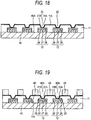
- Fig. 1 is a cross-sectional view of a related-art wiring substrate.
- a related-art wiring substrate 100 includes resin layers 101, 106, and 111; pads 102; vias 103, 107, and 112; and wiring lines 104, 108, and 113.
- the wiring substrate 100 is a coreless substrate.
- the resin layer 101 is provided so as to cover upper surfaces and side surfaces of the respective pads 102.
- the resin layer 101 has opening sections 115 through which upper surfaces (specifically, upper surfaces 117A of a Ni layer 117) of the pads 102 are exposed.
- the pad 102 has an Au layer 116 and an Ni layer 117.
- the Au layer 116 is provided on the resin layer 101.
- a lower surface 116A of an Au layer 116 is made essentially flush with a lower surface 101B of the resin layer 101.
- the Ni layer 117 is provided on the Au layer 116. Portions of the side and upper surfaces of the Ni layer 117 are covered with the resin layer 101.
- the Ni layer 117 has a function of preventing diffusion of Cu included in the vias 103 into the Au layer 116.
- the pads 102 are pads for connection with a semiconductor chip or pads functioning as external connection terminals.
- the vias 103 are provided in the opening sections 115.
- Each of the vias 103 has a seed layer 121 covering the opening section 115 and a Cu film 122 provided on the seed layer 121.
- a lower end of each of the vias 103 is connected to the Ni layer 117.
- the wiring lines 104 are provided over an upper surface 101A of the resin layer 101 from upper end portions of the vias 103.
- the wiring lines 104 are provided integrally with the respective vias 103, and each of the wiring lines 104 has the seed layer 121 provided on the upper surface 101A of the resin layer 101 and the Cu film 122 provided on the via 103 and the seed layer 121.
- the resin layer 106 is provided on the resin layer 101 so as to cover portions of the wiring lines 104.
- the resin layer 106 has an opening section 124 through which portions of the upper surface of the wiring line 104 are exposed.
- the vias 107 are provided in the respective opening sections 124.
- Each of the vias 107 has a seed layer 126 covering the opening section 124 and a Cu film 127 provided on the seed layer 126.
- a lower end of each of the vias 107 is connected to the wiring line 104.
- the wiring lines 108 are provided over an upper surface 106A of the resin layer 106 from upper end portions of the vias 107.
- the wiring lines 108 are provided integrally with the respective vias 107, and each of the wiring lines 108 has the seed layer 126 provided on the upper surface 106A of the resin layer 106 and the Cu film 127 provided on the via 107 and the seed layer 126.
- the resin layer 111 is provided over the resin layer 106 so as to cover portions of the wiring lines 108.
- the resin layers 111 have opening sections 131 through which portions of the upper surface of the wiring line 108 are exposed.
- the vias 112 are provided in the respective opening sections 131.
- Each of the vias 112 has a seed layer 133 covering the opening section 131 and a Cu film 134 provided on the seed layer 133.
- a lower end of each of the vias 112 is connected to the wiring line 108.
- the wiring lines 113 are provided over an upper surface 111A of the resin layer 111 from upper end portions of the vias 112.
- the wiring lines 113 are provided integrally with the respective vias 112.
- Each of the wiring lines 113 has the seed layer 133 provided on the upper surface 111A of the resin layer 111 and the Cu film 134 provided on the via 112 and the seed layer 133.
- Figs. 2 through 12 are views showing process for manufacturing the related-art wiring substrate.
- structures identical with those of the wiring substrate 100 shown in Fig. 1 are assigned the same reference numerals.
- a metal plate 136 serving as a support plate at the time of formation of the wiring substrate 100 is prepared.
- a resist film 138 having opening sections 138A is formed on the metal plate 136.
- an Au layer 116 and an Ni layer 117 are sequentially provided on a metal plate 136 exposed through the opening sections 138A by Cu electroplating, thereby forming the pads 102.
- the resist film 138 shown in Fig. 4 is eliminated, and the resin layer 101 having the opening sections 115 is formed over the metal plate 136 and the pads 102.
- the opening sections 115 are formed by means of; for example, subjecting the resin layer 101 to laser processing.
- the seed layer 121 is formed by electroless Cu plating so as to cover the upper layer 101A of the resin layer 101 and side surfaces and bottom surfaces of the opening sections 115.
- a resist film 141 having opening sections 141A is formed over the seed layer 121.
- the Cu film 122 is formed on the seed layer 121 exposed through the opening sections 141A by means of electrolytic plating during which the seed layer 121 is taken as a feeding layer.
- the vias 103 are formed in the respective opening sections 115.
- the resist film 141 shown in Fig. 8 is eliminated.
- the seed layer 121 which is not covered with the Cu film 122 (see Fig. 9 ) is etched away. Thereby, the wiring lines 104 are formed.
- the metal plate 136 shown in Fig. 11 is etched away. Thereby, the wiring substrate 100 is manufactured (see., e.g., International Publication No. 2003/039219 Brochure (Patent Document 1)).
- the Ni layer 117 is easy to be subject to oxidation, an oxide of Ni is formed on the upper surface of the Ni layer 117 of the structure shown in Fig. 5 . Therefore, when the Ni layer 117 on which the oxide is formed is connected to the vias 103, there arises a problem of a failure to sufficiently ensure the reliability of an electrical connection between the pads 102 and the vias 103 as a result of a decrease in adhesion between the pads 102 and the vias 103.
- a method for manufacturing a wiring substrate according to claim 1 comprising a pad formation process for forming a pad including a plurality of metal layers, the plurality of metal layers having a metal layer exposed through the wiring substrate, a first metal layer which is provided on the metal layer and which prevents diffusion of metal included in a via into the metal layer, and a second metal layer which is provided on the first metal layer and which is less subject to oxidation than the first metal layer; and a via formation process for forming the via on the second metal layer.
- the pad formation process may include a first and second metal layer formation process for continuously forming the first metal layer and the second metal layer by means of plating.
- the first metal layer and the second metal layer that is less subject to oxidation than the first metal layer are formed continuously by means of plating, thereby reducing a time during which the first metal layer is oxidized. Hence, adhesion between the first metal layer and the second metal layer can be enhanced.
- the reliability of electrical connection between pads and vias can be ensured sufficiently.
- Fig. 13 is a cross-sectional view of a wiring substrate of a first example.
- a wiring substrate 10 has insulation layers 11, 16, and 21; pads 12; vias 13, 17, and 22; and wiring lines 14, 18, and 23.
- the insulation layer 11 is provided so as to cover an upper surface (an upper surface of a metal layer 28 which is less subject to oxidation) and side surfaces of each of the pads 12.
- the insulation layer 11 has opening sections 25 through which upper surfaces (specifically, the upper surface of the metal layer 28 that is less subject to oxidation) of the pads 12 are exposed.
- a resin layer for example, polyimide, epoxy, or the like, can be used as the insulation layer 11.
- Each of the pads 12 is structured in such a way that a metal layer 26, a metal layer 27 (a first metal layer), and the metal layer 28 (a second metal layer) which is less subject to oxidation) are sequentially provided.
- the metal layer 26 is provided on the insulation layer 11. Side surfaces of the metal layer 26 are covered with the insulation layer 11. A lower surface 26A of the metal layer 26 is made essentially flush with a lower surface 11B of the insulation layer 11. The lower surface 26A of the metal layer 26 is exposed through the insulation layer 11.
- an Au layer, an Sn layer, an SnAg layer an alloy formed from Sn and Ag by means of plating, and the like, can be used.
- the thickness of the metal layer 26 can be set to; for example, 0.1 ⁇ m.
- the metal layer 27 is provided on the metal layer 26. Side surfaces of the metal layer 27 are covered with the insulation layer 11.
- the metal layer 27 is a layer for preventing diffusion of metal (specifically Cu) included in the vias 13 from diffusing into the metal layer 26, and have the property of being easy to be subject to oxidation.
- the metal layer 27 is formed from metal, whose change amount of free energy ⁇ F converted as a result of oxidation of metal per gram atom of oxygen is less than -32 kcal.
- an Ni layer can be used as the metal layer 27.
- the change amount of free energy ⁇ F converted as a result of oxidation of Ni per gram atom of oxygen is -46.1 kcal.
- the thickness of the metal layer 27 can be set to; for example, 10 ⁇ m.
- the metal layer 28 is a metal layer which is less subject oxidation than the metal layer 27, and provided on the metal layer 27. Portions of side surfaces and an upper surface of the metal layer 28 are covered with the insulation layer 11. An upper portion of the metal layer 28 is connected to the respective vias 13.
- a Cu layer, an Ag layer, an Au layer, a Pd layer, and the like can be used as the metal layer 28 that is less subject to oxidation.
- the thickness of the metal layer 28 can be set to; for example, 10 ⁇ m.
- a layer formed by stacking at least two of the Cu layer, the Ag layer, the Au layer, and the Pd layer may also be used as the metal layer 28.
- the metal layer 28 that is less subject to oxidation than the metal layer 27 is provided on the metal layer 27 that is easy to be subject to oxidation, and the metal layer 28 and the vias 13 are connected together, thereby preventing presence of an oxide between the pads 12 and the vias 13. Thereby, in order to enhance adhesion between the pads 12 and the vias 13, the reliability of electrical connection between the pads 12 and the vias 13 can be ensured sufficiently.
- the pads 12 formed as mentioned above are pads for use in connection with a semiconductor chip or serve as external connection terminals.
- the vias 13 are provided in respective opening sections 25 formed in the insulation layer 11. Lower ends of the vias 13 are connected to the metal layer 28 that is one of the constituent elements of the pads 12.
- Each of the vias 13 has a seed layer 31A and a Cu film 32A.
- the seed layer 31A is provided so as to cover the insulation layer 11 located on the side surfaces of the opening sections 25 and the upper surface of the metal layer 28 exposed through the opening sections 25.
- the seed layer 31A is a feeding layer used at the time of formation of the Cu film 32A by means of electrolytic plating.
- a Cu layer formed by means of; for example, sputtering, vacuum evaporation, electroless plating, or the like, can be used as the seed layer 31A.
- the Cu film 32A is provided so as to fill the opening sections 25 where the seed layer 31A is formed.
- the wiring lines 14 are provided so as to extend over the upper surface 11A of the insulation layer 11 from upper end portions of the respective vias 13.
- the wiring lines 14 are connected to the respective vias 13.
- Each of the wiring lines 14 has a seed layer 31B and a Cu film 32B.
- the seed layer 31B is provided on the upper surface 11A of the insulation layer 11 located in the vicinity of the opening sections 25.
- the seed layer 31B is a feeding layer used when the Cu film 32B is formed by means of electrolytic plating.
- a Cu layer formed by means of; for example, sputtering, vacuum deposition, electroless plating, or the like, can be used as the seed layer 31B.
- the insulation layer 16 is provided on the upper surface 11A of the insulation layer 11 so as to cover portions of the wiring lines 14.
- the insulation layer 16 has opening sections 34 through which portions of upper surfaces of the wiring lines 14 are exposed.
- a resin layer for example, polyimide, an epoxy, or the like, can be used as the insulation layer 16.
- Vias 17 are provided in the respective opening sections 34 formed in the insulation layer 16.
- the vias 17 are connected to the wiring lines 14.
- Each of the vias 17 has a seed layer 36A and a Cu film 37A.
- the seed layer 36A is provided so as to cover the insulation layer 16 located on the side surfaces of the respective opening sections 34 and the upper surface of the wiring lines 14 exposed through the opening sections 34.
- the seed layer 36A is a feeding layer used when the Cu film 37A is formed by means of electrolytic plating.
- a Cu layer formed by means of; for example, sputtering, vacuum deposition, electroless plating, or the like, can be used for the seed layer 36A.
- the Cu film 37A is provided so as to fill the opening sections 34 formed in the seed layer 36A.
- the wiring lines 18 are provided so as to extend over an upper surface 16A of the insulation layer 16 from upper end portions of the respective vias 17.
- the wiring lines 18 are connected to the vias 17.
- Each of the wiring lines 18 has a seed layer 36B and a Cu film 37B.
- the seed layer 36B is provided on the upper surface 16A of the insulation layer 16 located in the vicinity of the opening sections 34.
- the seed layer 36B is a feeding layer used when the Cu film 37B is formed by means of electrolytic plating.
- a Cu layer formed by means of; for example, sputtering, vacuum deposition, electroless plating, or the like, can be used as the seed layer 36B.
- the insulation layer 21 is provided on the upper surface 16A of the insulation layer 16 so as to cover portions of the wiring lines 18.
- the insulation layer 21 has opening sections 39 through which portions of upper surfaces of the wiring lines 18 are exposed.
- a resin layer for example, polyimide, an epoxy, or the like, can be used as the insulation layer 21.
- Vias 22 are provided in the respective opening sections 39 formed in the insulation layer 21.
- the vias 22 are connected to the wiring lines 18.
- Each of the vias 22 has a seed layer 41A and a Cu film 42A.
- the seed layer 41A is provided so as to cover the insulation layer 21 located on the side surfaces of the respective opening sections 39 and the upper surface of the wiring lines 18 exposed through the opening sections 39.
- the seed layer 41A is a feeding layer used when the Cu film 42A is formed by means of electrolytic plating.
- a Cu layer formed by means of; for example, sputtering, vacuum deposition, electroless plating, or the like, can be used for the seed layer 41A.
- the Cu film 42A is provided so as to fill the opening sections 39 formed in the seed layer 41A.
- the wiring lines 23 are provided so as to extend over an upper surface 21A of the insulation layer 21 from upper end portions of the respective vias 22.
- the wiring lines 23 are connected to the vias 22.
- Each of the wiring lines 23 has a seed layer 41B and a Cu film 42B.
- the seed layer 41B is provided on the upper surface 21A of the insulation layer 21 located in the vicinity of the opening sections 39.
- the seed layer 41B is a feeding layer used when the Cu film 42B is formed by means of electrolytic plating.
- a Cu layer formed by means of; for example, sputtering, vacuum deposition, electroless plating, or the like, can be used as the seed layer 41B.
- the metal layer 28 that is less subject to oxidation than the metal layer 27 is provided on the metal layer 27 that is easy to be subject to oxidation, and the vias 13 and the metal layer 28 that is a constituent element of the pads 12 are connected together, thereby preventing presence of an oxide between the pads 12 and the vias 13.
- adhesion between the pads 12 and the vias 13 is enhanced, and the reliability of electrical connection between the pads 12 and the vias 13 can be ensured sufficiently.
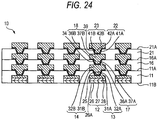
- Figs. 14 through 24 are views showing processes for manufacturing the wiring substrate.
- constituent elements which are the same as those of the wiring substrate 10 are assigned the same reference numerals.
- a metal plate 46 serving as a support plate at the time of manufacture of the wiring substrate 10 is prepared.
- a Cu plate can be used as the metal plate 46.
- the thickness of the metal plate can be set to; for example, 0.3 mm.
- Metal foil may also be used in lieu of the metal plate 46.
- a resist film 47 having opening sections 47A is formed on the metal plate 46.
- the opening sections 47A are formed in such a way that areas of an upper surface 46A of the metal plate 46 corresponding to the areas, where the pads 12 are formed, become exposed.
- the metal layer 26, the metal layer 27 that is easy to be subject to oxidation, and the metal layer 28 that is less subject to oxidation than the metal layer 27 are continuously formed, by means of electrolytic plating during which the metal plate 46 is taken as a feeding layer, on areas of the upper surface 46A of the metal plate 46 exposed through the opening sections 47A (first and secondmetal layer formation processes).
- the pads 12 formed from the metal layers 26 to 28 are formed on the metal plate 46.
- the metal layers 26 to 28 are formed by use of a single plating apparatus.
- a plating apparatus having a first plating bath filled with a plating solution used for forming the metal plate 26, a second plating bath filled with a plating fluid filled with a plating solution used for forming the metal plate 27, and a third plating bath filled with a plating solution used for forming the metal layer 28.
- the metal layer 28 that is less subject to oxidation than the metal layer 27 can be formed on the metal layer 27 immediately after formation of the metal layer 27 that is easy to be subject to oxidation.
- a time during which an oxide is formed on the metal layer 27 is reduced, so that sufficient adhesion between the metal layer 27 and the metal layer 28 can be ensured sufficiently.
- an Au layer, an Sn layer, SnAg layer (an alloy formed from Sn and Ag by means of plating), or the like, can be used as the metal layer 26.
- the thickness of the metal layer 26 can be set to; for example, 0.1 ⁇ m.
- the metal layer 27 is formed from metal, whose change amount of free energy ⁇ F converted as a result of oxidation of metal per gram atom of oxygen is less than -32 kcal.
- an Ni layer can be used as the metal layer 27.
- the change amount of free energy ⁇ F converted as a result of oxidation of Ni per gram atom of oxygen is -46.1 kcal.
- the thickness of the metal layer 27 can be set to; for example, 10 ⁇ m.
- the metal layer 28 that is less subject to oxidation is a metal layer formed from metal, whose change amount of free energy ⁇ F converted as a result of oxidation of metal per gram atom of oxygen is greater than -32 kcal.
- a Cu layer, an Ag layer, an Au layer, a Pd layer, and the like can be used as the metal layer 28.
- the thickness of the metal layer 28 can be set to; for example, 10 ⁇ m.
- a layer formed by stacking at least two of the Cu layer, the Ag layer, the Au layer, and the Pd layer may also be used as the metal layer 28.
- the resist film 47 shown in Fig. 16 is eliminated, and the insulation layer 11 having the opening sections 25 is formed over the metal plate 46 and the pads 12.
- the opening sections 25 are formed by means of subjecting the insulation layer 11 to laser processing. At this time, the opening sections 25 are formed in such a way that the upper surface of the metal layer 28 becomes exposed.
- a resin layer for example, an epoxy, polyimide, or the like, can be used as the insulation layer 11.
- a seed layer 31A which covers surfaces of the insulation layer 11 corresponding to the side surfaces of the respective opening sections 25 and areas of the upper surface of the metal layer 28 exposed through the opening sections 25, and a seed layer 31B covering the upper surface 11A of the insulation layer 11 are formed simultaneously.
- the seed layers 31A and 31B can be formed by means of; for example, sputtering, vacuum deposition, electroless plating, or the like.
- a Cu layer can be used for the seed layers 31A and 31B.
- the thickness of the seed layers 31A and 31B can be set to; for example, 3 ⁇ m.
- a resist film 49 having opening sections 49A is formed on the seed layer 31B.
- the opening sections 49A are formed in such a way that areas of the see layers 31A and 31B corresponding to the areas, where the vias 13 and the wiring lines 14 are formed, become exposed.
- the Cu films 32A and 32B are formed simultaneously on the seed layers 31A and 31B exposed through the opening sections 49A by means of electrolytic plating during which the seed layers 31A and 31B are taken as feeding layers.
- the vias 13, each of which is formed from the seed layer 31A and the Cu film 32A are formed in the respective opening sections 25 (a via formation process).
- the vias 13 are connected to the metal layer 28 which is less subject to oxidation.
- the metal layer 28 that is less subject to oxidation than the metal layer 27 and the vias 13 are connected together, thereby preventing presence of an oxide between the pads 12 and the vias 13. Thereby, adhesion between the pads 12 and the vias 13 is enhanced, and the reliability of electrical connection between the pads 12 and the vias 13 can be ensured sufficiently.
- the resist film 49 shown in Fig. 20 is eliminated.
- the seed layer 31B (see Fig. 21 ) which is not covered with the Cu film 32B (see Fig. 21 ) is etched away. Thereby, the wiring lines 14, each of which is formed from the seed layer 31B and the Cu film 32B, are formed.
- the metal plate 46 shown in Fig. 23 is etched away, whereby the wiring substrate 10 is manufactured.
- the metal layer 27, and the metal layer 28 that is less subject to oxidation than the metal layer 27, constituting the pads are continuously formed by means of plating.
- a time during which an oxide is formed on the metal layer 27 is reduced, so that sufficient adhesion between the metal layer 27 and the metal layer 28 can be ensured sufficiently.
- the metal layer 28 that is less subject to oxidation than the metal layer 27 and the vias 13 are connected together, thereby preventing presence of an oxide between the pads 12 and the vias 13. Thereby, adhesion between the pads 12 and the vias 13 is enhanced, and the reliability of electrical connection between the pads 12 and the vias 13 can be ensured sufficiently.
- a process for roughening the upper surface of the metal layer 28 may also be provided between the process shown in Fig. 16 and the process shown in Fig. 17 .
- adhesion between the pads 12 and the vias 13 can be enhanced.
- Roughening can be performed by means of roughening the upper surface of the metal layer 28 through use of an etchant.
- the Ni layer 117 that is easy to be subject to oxidation is provided in the uppermost layer of each of the pads 102.
- the oxide film is formed on the Ni layer 117.
- the metal layer 28 that is less subject to oxidation is roughened, thereby preventing formation of an oxide on the metal layer 28.
- adhesion between the pads 12 and the vias 13 can be enhanced.
- Fig. 25 is a cross-sectional view of a wiring substrate of a second example.
- constituent elements which are the same as those of the wiring substrate 10 of the first example are assigned the same reference numerals.
- a wiring substrate 60 of the second example is formed similarly to the wiring substrate 10 except that pads 61 are provided in place of the pads 12 provided in the wiring substrate 10 of the first example .
- Each of the pads 61 is structured such that the metal layer 26, a metal layer 63, the metal layer 27, and the metal layer 28 that is less subject to oxidation than the metal layer 27 are provided sequentially.
- the pads 61 are formed similarly to the pads 12 except that the metal layer 63 is provided between the metal layer 26 and the metal layer 27 in the pad 12 described in connection with the first example.
- the metal layer 63 has a function of preventing oxidation of the metal layer 26.
- a Pd layer can be used as the metal layer 63.
- the thickness of the metal layer 63 can be set to; for example, 0.1 ⁇ m.
- the metal layer 63 having the function of preventing oxidation of the metal layer 26 is provided between the metal layer 26 and the metal layer 27 that is easy to be subject to oxidation, whereby oxidation of the metal layer 26 can be prevented. Further, the wiring substrate 60 of the present example can obtain the same advantage as the wiring substrate 10 of the first example .
- the wiring substrate 60 of the present example can be manufactured by means of the same processes as the wiring substrate 10 of the first embodiment.
- the present invention can be applied to a wiring substrate having a pad which includes a metal layer exposed through a wiring substrate and a first metal interposed between the metal layer and vias for preventing diffusion of metal included in the vias into the metal layer and to a method for manufacturing the wiring substrate.
Priority Applications (1)
| Application Number | Priority Date | Filing Date | Title |
|---|---|---|---|
| EP12164665.7A EP2479788B1 (en) | 2006-12-04 | 2007-12-04 | Wiring substrate and method for manufacturing the same |
Applications Claiming Priority (1)
| Application Number | Priority Date | Filing Date | Title |
|---|---|---|---|
| JP2006327493A JP5214139B2 (ja) | 2006-12-04 | 2006-12-04 | 配線基板及びその製造方法 |
Related Child Applications (2)
| Application Number | Title | Priority Date | Filing Date |
|---|---|---|---|
| EP12164665.7A Division-Into EP2479788B1 (en) | 2006-12-04 | 2007-12-04 | Wiring substrate and method for manufacturing the same |
| EP12164665.7A Division EP2479788B1 (en) | 2006-12-04 | 2007-12-04 | Wiring substrate and method for manufacturing the same |
Publications (3)
| Publication Number | Publication Date |
|---|---|
| EP1930946A2 EP1930946A2 (en) | 2008-06-11 |
| EP1930946A3 EP1930946A3 (en) | 2009-09-09 |
| EP1930946B1 true EP1930946B1 (en) | 2017-01-25 |
Family
ID=39273240
Family Applications (2)
| Application Number | Title | Priority Date | Filing Date |
|---|---|---|---|
| EP07122244.2A Active EP1930946B1 (en) | 2006-12-04 | 2007-12-04 | Method for manufacturing wiring substrate |
| EP12164665.7A Active EP2479788B1 (en) | 2006-12-04 | 2007-12-04 | Wiring substrate and method for manufacturing the same |
Family Applications After (1)
| Application Number | Title | Priority Date | Filing Date |
|---|---|---|---|
| EP12164665.7A Active EP2479788B1 (en) | 2006-12-04 | 2007-12-04 | Wiring substrate and method for manufacturing the same |
Country Status (6)
| Country | Link |
|---|---|
| US (1) | US8476536B2 (ja) |
| EP (2) | EP1930946B1 (ja) |
| JP (1) | JP5214139B2 (ja) |
| KR (1) | KR101436035B1 (ja) |
| CN (1) | CN101198213A (ja) |
| TW (1) | TWI407852B (ja) |
Families Citing this family (25)
| Publication number | Priority date | Publication date | Assignee | Title |
|---|---|---|---|---|
| KR100881303B1 (ko) * | 2005-11-02 | 2009-02-03 | 이비덴 가부시키가이샤 | 반도체 장치용 다층 프린트 배선판 및 그 제조 방법 |
| JP5203108B2 (ja) | 2008-09-12 | 2013-06-05 | 新光電気工業株式会社 | 配線基板及びその製造方法 |
| JP2010118635A (ja) * | 2008-11-12 | 2010-05-27 | Ibiden Co Ltd | 多層プリント配線板 |
| US8686300B2 (en) | 2008-12-24 | 2014-04-01 | Ibiden Co., Ltd. | Printed wiring board and method for manufacturing the same |
| JP5561460B2 (ja) * | 2009-06-03 | 2014-07-30 | 新光電気工業株式会社 | 配線基板および配線基板の製造方法 |
| JP5355504B2 (ja) * | 2009-07-30 | 2013-11-27 | 株式会社東芝 | 半導体装置の製造方法および半導体装置 |
| JP5479073B2 (ja) * | 2009-12-21 | 2014-04-23 | 新光電気工業株式会社 | 配線基板及びその製造方法 |
| JP5603600B2 (ja) * | 2010-01-13 | 2014-10-08 | 新光電気工業株式会社 | 配線基板及びその製造方法、並びに半導体パッケージ |
| JP5716948B2 (ja) * | 2010-09-29 | 2015-05-13 | 日立化成株式会社 | 半導体素子搭載用パッケージ基板の製造方法 |
| JP2013093405A (ja) * | 2011-10-25 | 2013-05-16 | Ngk Spark Plug Co Ltd | 配線基板及びその製造方法 |
| JP5800674B2 (ja) * | 2011-10-25 | 2015-10-28 | 日本特殊陶業株式会社 | 配線基板及びその製造方法 |
| JP5580374B2 (ja) * | 2012-08-23 | 2014-08-27 | 新光電気工業株式会社 | 配線基板及びその製造方法 |
| JP5315447B2 (ja) * | 2012-09-03 | 2013-10-16 | 新光電気工業株式会社 | 配線基板及びその製造方法 |
| KR20140030918A (ko) * | 2012-09-04 | 2014-03-12 | 삼성전기주식회사 | 인쇄회로기판 |
| JP5493020B2 (ja) * | 2013-03-08 | 2014-05-14 | 新光電気工業株式会社 | 配線基板の製造方法及び半導体パッケージの製造方法 |
| US9165878B2 (en) * | 2013-03-14 | 2015-10-20 | United Test And Assembly Center Ltd. | Semiconductor packages and methods of packaging semiconductor devices |
| US9653419B2 (en) * | 2015-04-08 | 2017-05-16 | Intel Corporation | Microelectronic substrate having embedded trace layers with integral attachment structures |
| US10115579B2 (en) * | 2016-11-30 | 2018-10-30 | Asm Technology Singapore Pte Ltd | Method for manufacturing wafer-level semiconductor packages |
| TWI633822B (zh) * | 2017-05-08 | 2018-08-21 | 欣興電子股份有限公司 | 線路板單元與其製作方法 |
| WO2019066977A1 (en) * | 2017-09-29 | 2019-04-04 | Intel Corporation | FIRST-LEVEL THIN-LEVEL INTERCONNECTIONS DEFINED BY AUTOCATALYTIC METAL FOR LITHOGRAPHIC INTERCONNECTION HOLES |
| CN109712897B (zh) * | 2017-10-26 | 2020-12-18 | 中芯国际集成电路制造(上海)有限公司 | 一种半导体器件及其制作方法、电子装置 |
| CN111343802B (zh) * | 2018-12-19 | 2022-02-22 | 庆鼎精密电子(淮安)有限公司 | 电路板及其制作方法 |
| KR20210009528A (ko) * | 2019-07-17 | 2021-01-27 | 삼성전기주식회사 | 코일 부품 |
| KR20210142300A (ko) * | 2020-05-18 | 2021-11-25 | 삼성전기주식회사 | 코일 부품 |
| US20220312591A1 (en) * | 2021-03-26 | 2022-09-29 | Juniper Networks, Inc. | Substrate with conductive pads and conductive layers |
Citations (1)
| Publication number | Priority date | Publication date | Assignee | Title |
|---|---|---|---|---|
| EP1259103A1 (en) * | 2000-02-25 | 2002-11-20 | Ibiden Co., Ltd. | Multilayer printed wiring board and method for producing multilayer printed wiring board |
Family Cites Families (17)
| Publication number | Priority date | Publication date | Assignee | Title |
|---|---|---|---|---|
| US5440805A (en) * | 1992-03-09 | 1995-08-15 | Rogers Corporation | Method of manufacturing a multilayer circuit |
| US5274912A (en) * | 1992-09-01 | 1994-01-04 | Rogers Corporation | Method of manufacturing a multilayer circuit board |
| US5309629A (en) * | 1992-09-01 | 1994-05-10 | Rogers Corporation | Method of manufacturing a multilayer circuit board |
| DE69936235T2 (de) | 1998-02-26 | 2007-09-13 | Ibiden Co., Ltd., Ogaki | Mehrschichtige Leiterplatte mit gefüllten Kontaktlöchern |
| MY139405A (en) * | 1998-09-28 | 2009-09-30 | Ibiden Co Ltd | Printed circuit board and method for its production |
| US6406991B2 (en) | 1999-12-27 | 2002-06-18 | Hoya Corporation | Method of manufacturing a contact element and a multi-layered wiring substrate, and wafer batch contact board |
| JP3664720B2 (ja) | 2001-10-31 | 2005-06-29 | 新光電気工業株式会社 | 半導体装置用多層回路基板の製造方法 |
| JP2003179358A (ja) * | 2002-10-28 | 2003-06-27 | Ibiden Co Ltd | フィルビア構造を有する多層プリント配線板 |
| TWI263704B (en) | 2003-03-18 | 2006-10-11 | Ngk Spark Plug Co | Wiring board |
| JP4699704B2 (ja) * | 2003-03-18 | 2011-06-15 | 日本特殊陶業株式会社 | 配線基板 |
| CN100390951C (zh) * | 2003-03-25 | 2008-05-28 | 富士通株式会社 | 电子部件安装基板的制造方法 |
| JP4108643B2 (ja) * | 2004-05-12 | 2008-06-25 | 日本電気株式会社 | 配線基板及びそれを用いた半導体パッケージ |
| US7179738B2 (en) * | 2004-06-17 | 2007-02-20 | Texas Instruments Incorporated | Semiconductor assembly having substrate with electroplated contact pads |
| KR100601485B1 (ko) | 2004-12-30 | 2006-07-18 | 삼성전기주식회사 | Bga 패키지 기판 및 그 제조방법 |
| JP4776247B2 (ja) * | 2005-02-09 | 2011-09-21 | 富士通株式会社 | 配線基板及びその製造方法 |
| JP4781718B2 (ja) | 2005-05-27 | 2011-09-28 | 富士重工業株式会社 | バッテリ固定構造 |
| JP2007035734A (ja) * | 2005-07-25 | 2007-02-08 | Nec Electronics Corp | 半導体装置およびその製造方法 |
-
2006
- 2006-12-04 JP JP2006327493A patent/JP5214139B2/ja active Active
-
2007
- 2007-12-03 KR KR1020070124500A patent/KR101436035B1/ko active IP Right Grant
- 2007-12-03 US US11/987,617 patent/US8476536B2/en active Active
- 2007-12-04 EP EP07122244.2A patent/EP1930946B1/en active Active
- 2007-12-04 CN CNA2007101959256A patent/CN101198213A/zh active Pending
- 2007-12-04 TW TW096146072A patent/TWI407852B/zh active
- 2007-12-04 EP EP12164665.7A patent/EP2479788B1/en active Active
Patent Citations (1)
| Publication number | Priority date | Publication date | Assignee | Title |
|---|---|---|---|---|
| EP1259103A1 (en) * | 2000-02-25 | 2002-11-20 | Ibiden Co., Ltd. | Multilayer printed wiring board and method for producing multilayer printed wiring board |
Also Published As
| Publication number | Publication date |
|---|---|
| CN101198213A (zh) | 2008-06-11 |
| JP2008141070A (ja) | 2008-06-19 |
| KR101436035B1 (ko) | 2014-09-01 |
| EP2479788A2 (en) | 2012-07-25 |
| KR20080051093A (ko) | 2008-06-10 |
| TW200833201A (en) | 2008-08-01 |
| US8476536B2 (en) | 2013-07-02 |
| EP2479788A3 (en) | 2015-02-25 |
| EP1930946A3 (en) | 2009-09-09 |
| TWI407852B (zh) | 2013-09-01 |
| EP1930946A2 (en) | 2008-06-11 |
| JP5214139B2 (ja) | 2013-06-19 |
| EP2479788B1 (en) | 2017-05-03 |
| US20080149383A1 (en) | 2008-06-26 |
Similar Documents
| Publication | Publication Date | Title |
|---|---|---|
| EP1930946B1 (en) | Method for manufacturing wiring substrate | |
| US9515018B2 (en) | Wiring substrate and method for manufacturing wiring substrate | |
| CN1921079B (zh) | 配线基板的制造方法 | |
| US8039756B2 (en) | Multilayered wiring board, semiconductor device in which multilayered wiring board is used, and method for manufacturing the same | |
| US7791186B2 (en) | Wiring board, semiconductor device in which wiring board is used, and method for manufacturing the same | |
| JP5392847B2 (ja) | 配線基板、半導体装置及びそれらの製造方法 | |
| KR20080091709A (ko) | 배선 기판 및 그 제조 방법 | |
| CN101315917A (zh) | 配线基板及其制造方法 | |
| JP2017157666A (ja) | 配線基板、半導体装置、配線基板の製造方法及び半導体装置の製造方法 | |
| US20180211909A1 (en) | Package substrate, method for fabricating the same, and package device including the package substrate | |
| US8066862B2 (en) | Manufacturing method of wiring board | |
| JP2008283226A (ja) | 半導体装置搭載用配線基板およびその製造方法、並びに半導体パッケージ | |
| JP4547164B2 (ja) | 配線基板の製造方法 | |
| JP4975581B2 (ja) | 配線基板及びその製造方法 | |
| JP6457881B2 (ja) | 配線基板及びその製造方法 | |
| JP4445778B2 (ja) | 配線基板の製造方法 | |
| JP4730072B2 (ja) | 回路基板の製造方法 | |
| US11558959B2 (en) | Printed circuit board | |
| JP2012138632A (ja) | 配線基板及びその製造方法 | |
| JP4509747B2 (ja) | プリント配線板の製造方法 | |
| JP2009141298A (ja) | 多層配線板及びその製造方法 | |
| JP2008159797A (ja) | 半導体装置およびその製造方法 |
Legal Events
| Date | Code | Title | Description |
|---|---|---|---|
| PUAI | Public reference made under article 153(3) epc to a published international application that has entered the european phase |
Free format text: ORIGINAL CODE: 0009012 |
|
| AK | Designated contracting states |
Kind code of ref document: A2 Designated state(s): AT BE BG CH CY CZ DE DK EE ES FI FR GB GR HU IE IS IT LI LT LU LV MC MT NL PL PT RO SE SI SK TR |
|
| AX | Request for extension of the european patent |
Extension state: AL BA HR MK RS |
|
| PUAL | Search report despatched |
Free format text: ORIGINAL CODE: 0009013 |
|
| AK | Designated contracting states |
Kind code of ref document: A3 Designated state(s): AT BE BG CH CY CZ DE DK EE ES FI FR GB GR HU IE IS IT LI LT LU LV MC MT NL PL PT RO SE SI SK TR |
|
| AX | Request for extension of the european patent |
Extension state: AL BA HR MK RS |
|
| 17P | Request for examination filed |
Effective date: 20100222 |
|
| AKX | Designation fees paid |
Designated state(s): DE FR GB |
|
| 17Q | First examination report despatched |
Effective date: 20100422 |
|
| GRAP | Despatch of communication of intention to grant a patent |
Free format text: ORIGINAL CODE: EPIDOSNIGR1 |
|
| INTG | Intention to grant announced |
Effective date: 20160810 |
|
| GRAS | Grant fee paid |
Free format text: ORIGINAL CODE: EPIDOSNIGR3 |
|
| GRAA | (expected) grant |
Free format text: ORIGINAL CODE: 0009210 |
|
| AK | Designated contracting states |
Kind code of ref document: B1 Designated state(s): DE FR GB |
|
| REG | Reference to a national code |
Ref country code: GB Ref legal event code: FG4D |
|
| REG | Reference to a national code |
Ref country code: DE Ref legal event code: R096 Ref document number: 602007049624 Country of ref document: DE |
|
| REG | Reference to a national code |
Ref country code: DE Ref legal event code: R097 Ref document number: 602007049624 Country of ref document: DE |
|
| REG | Reference to a national code |
Ref country code: FR Ref legal event code: PLFP Year of fee payment: 11 |
|
| PLBE | No opposition filed within time limit |
Free format text: ORIGINAL CODE: 0009261 |
|
| STAA | Information on the status of an ep patent application or granted ep patent |
Free format text: STATUS: NO OPPOSITION FILED WITHIN TIME LIMIT |
|
| 26N | No opposition filed |
Effective date: 20171026 |
|
| PGFP | Annual fee paid to national office [announced via postgrant information from national office to epo] |
Ref country code: GB Payment date: 20231102 Year of fee payment: 17 |
|
| PGFP | Annual fee paid to national office [announced via postgrant information from national office to epo] |
Ref country code: FR Payment date: 20231108 Year of fee payment: 17 Ref country code: DE Payment date: 20231031 Year of fee payment: 17 |