EP1929559B1 - Method for inhibiting oxygen and moisture degradation of a device and the resulting device - Google Patents
Method for inhibiting oxygen and moisture degradation of a device and the resulting device Download PDFInfo
- Publication number
- EP1929559B1 EP1929559B1 EP06800857.2A EP06800857A EP1929559B1 EP 1929559 B1 EP1929559 B1 EP 1929559B1 EP 06800857 A EP06800857 A EP 06800857A EP 1929559 B1 EP1929559 B1 EP 1929559B1
- Authority
- EP
- European Patent Office
- Prior art keywords
- llt
- glass
- tin
- layers
- oxygen
- Prior art date
- Legal status (The legal status is an assumption and is not a legal conclusion. Google has not performed a legal analysis and makes no representation as to the accuracy of the status listed.)
- Ceased
Links
Images



Classifications
-
- H—ELECTRICITY
- H10—SEMICONDUCTOR DEVICES; ELECTRIC SOLID-STATE DEVICES NOT OTHERWISE PROVIDED FOR
- H10K—ORGANIC ELECTRIC SOLID-STATE DEVICES
- H10K50/00—Organic light-emitting devices
- H10K50/80—Constructional details
- H10K50/84—Passivation; Containers; Encapsulations
- H10K50/844—Encapsulations
-
- C—CHEMISTRY; METALLURGY
- C03—GLASS; MINERAL OR SLAG WOOL
- C03C—CHEMICAL COMPOSITION OF GLASSES, GLAZES OR VITREOUS ENAMELS; SURFACE TREATMENT OF GLASS; SURFACE TREATMENT OF FIBRES OR FILAMENTS MADE FROM GLASS, MINERALS OR SLAGS; JOINING GLASS TO GLASS OR OTHER MATERIALS
- C03C3/00—Glass compositions
- C03C3/12—Silica-free oxide glass compositions
- C03C3/122—Silica-free oxide glass compositions containing oxides of As, Sb, Bi, Mo, W, V, Te as glass formers
-
- B—PERFORMING OPERATIONS; TRANSPORTING
- B05—SPRAYING OR ATOMISING IN GENERAL; APPLYING FLUENT MATERIALS TO SURFACES, IN GENERAL
- B05D—PROCESSES FOR APPLYING FLUENT MATERIALS TO SURFACES, IN GENERAL
- B05D5/00—Processes for applying liquids or other fluent materials to surfaces to obtain special surface effects, finishes or structures
-
- C—CHEMISTRY; METALLURGY
- C03—GLASS; MINERAL OR SLAG WOOL
- C03C—CHEMICAL COMPOSITION OF GLASSES, GLAZES OR VITREOUS ENAMELS; SURFACE TREATMENT OF GLASS; SURFACE TREATMENT OF FIBRES OR FILAMENTS MADE FROM GLASS, MINERALS OR SLAGS; JOINING GLASS TO GLASS OR OTHER MATERIALS
- C03C3/00—Glass compositions
- C03C3/12—Silica-free oxide glass compositions
- C03C3/14—Silica-free oxide glass compositions containing boron
-
- C—CHEMISTRY; METALLURGY
- C03—GLASS; MINERAL OR SLAG WOOL
- C03C—CHEMICAL COMPOSITION OF GLASSES, GLAZES OR VITREOUS ENAMELS; SURFACE TREATMENT OF GLASS; SURFACE TREATMENT OF FIBRES OR FILAMENTS MADE FROM GLASS, MINERALS OR SLAGS; JOINING GLASS TO GLASS OR OTHER MATERIALS
- C03C3/00—Glass compositions
- C03C3/12—Silica-free oxide glass compositions
- C03C3/23—Silica-free oxide glass compositions containing halogen and at least one oxide, e.g. oxide of boron
- C03C3/247—Silica-free oxide glass compositions containing halogen and at least one oxide, e.g. oxide of boron containing fluorine and phosphorus
-
- H—ELECTRICITY
- H05—ELECTRIC TECHNIQUES NOT OTHERWISE PROVIDED FOR
- H05B—ELECTRIC HEATING; ELECTRIC LIGHT SOURCES NOT OTHERWISE PROVIDED FOR; CIRCUIT ARRANGEMENTS FOR ELECTRIC LIGHT SOURCES, IN GENERAL
- H05B33/00—Electroluminescent light sources
- H05B33/02—Details
- H05B33/04—Sealing arrangements, e.g. against humidity
-
- H—ELECTRICITY
- H10—SEMICONDUCTOR DEVICES; ELECTRIC SOLID-STATE DEVICES NOT OTHERWISE PROVIDED FOR
- H10K—ORGANIC ELECTRIC SOLID-STATE DEVICES
- H10K59/00—Integrated devices, or assemblies of multiple devices, comprising at least one organic light-emitting element covered by group H10K50/00
- H10K59/80—Constructional details
- H10K59/87—Passivation; Containers; Encapsulations
- H10K59/873—Encapsulations
Definitions
- the present invention relates to a method for inhibiting oxygen and moisture penetration, and subsequent degradation of a device and the resulting device.
- this device include a light-emitting device (e.g., organic light emitting diode (OLED) device), a photovoltaic device, a thin-film sensor, an evanescent waveguide sensor, a food container and a medicine container.
- a light-emitting device e.g., organic light emitting diode (OLED) device
- a photovoltaic device e.g., a photovoltaic device
- a thin-film sensor e.g., an evanescent waveguide sensor
- a food container e.g., a medicine container.
- OLED devices The more prominent efforts to extend the lifetime of OLED devices include gettering, encapsulation and extensive device sealing techniques.
- Today one common way for sealing an OLED device is to use different types of epoxies, inorganic materials and/or organic materials that form a seal after they are cured by ultra-violet light, or heated by various means.
- Vitex Systems manufactures and offers for sale a coating under the brand name of Barix TM which is a composite based approach where alternate layers of inorganic materials and organic materials are used to seal the entire surface of the OLED device.
- Barix TM which is a composite based approach where alternate layers of inorganic materials and organic materials are used to seal the entire surface of the OLED device.
- US Patent 3 795 976 relates to a method of producing a semiconductor device provided with a composite passivating film which comprises depositing silicon dioxide on the free surface of a semiconductor wafer from an atmosphere containing oxygen and a vapour of a decomposable volatile organic silicon compound followed by forming a tantalum pentoxide film on the silicon dioxide film by reactive sputtering of tantalum in an oxygen containing atmosphere. The wafer is then subjected to heat treatment in a non-reducing atmosphere.
- German Offenlegungsschrift 24 31 917 relates to a semiconductor element provided with a multi-layer passivating film comprising a phosphorus glass layer and overlying boron glass layer.
- EP 1 278 244 A2 relates to a panel display device formed using organic electroluminescence which is provided with a multi-layer sealing structure which includes a first (inner) protective layer of a high polymer compound containing fluorine, a second protective layer formed of a silicon composite, a third protective layer formed of a compound hardened by polymerisation at room temperature and normal pressure and a fourth (outer) protective layer formed of a number of layers adhered to one other.
- the fourth protective layer may include as one of the number of layers a layer of a glass of low melting temperature.
- EP 0 638 939 A2 relates to a solar cell including a substrate, a compound semiconductor which is a laminated film having a number of semiconductor layers and layers of low melting point glass above and below the semiconductor layers so that on heating the low melting point glass seals the semiconductor layers against release into the air of toxic substances that they may contain.
- US Patent 5 089 446 relates to a family of glass compositions in the tin-phosphorus oxyfluoride system that exhibit very low glass transition temperature and coefficients of thermal expansion (25-150°C) not over about 160x10 -7 / °C.
- the glasses contain up to 11% Nb and may additionally contain up to 10%, taken individually or in combination, of V, Fe and/or Mo to further decrease Tg and CTE values.
- the glasses are suitable for forming fusion-type seals.
- US 6306783 discloses a method of sealing an electronic device with a tin borophosphate glass composition.
- the present invention provides a method for inhibiting oxygen and moisture penetration of a device comprising a substrate and one or more inner layers, characterized in that a tin fluorophosphate material is deposited by sputtering over the one or more inner layers located on top of the substrate of the device and the deposited tin fluorophosphate material is heat treated to form a pore-free barrier layer, said deposition and heat treatment of the tin fluorophosphate material taking place in a vacuum or in an inert atmosphere to maintain an oxygen and water free environment.
- the present invention provides an organic electronic device comprising a substrate plate and at least one organic electronic or optoelectronic layer, characterized in that the device also comprises a barrier layer of a tin fluorophosphate material, the at least one electronic or optoelectronic layer being hermetically sealed between the tin fluorophosphate material and the substrate plate.
- the present invention utilizes an LLT (low liquidus temperature) material, which in specific embodiments has a low glass transition temperature, to form a barrier layer on a device.
- the LLT material is a tin fluorophosphate material which includes, but is not limited to, tin fluorophosphate glass.
- the LLT material is deposited onto the device by sputtering. Defects in the LLT material from the deposition step are removed by a consolidation step i.e., by (heat treatment), to produce a pore-free, gas and moisture impenetrable protective coating on the device.
- a consolidation step i.e., by (heat treatment)
- the consolidation step is only practical with the LLT material where the consolidation temperature is sufficiently low so as to not damage the inner layers in the device.
- the deposition step and the heat treatment step take place in a a vacuum or in an inert atmosphere.
- the device 200 includes a heat treated low liquidus temperature (LLT) material 202, one or more inner layers 204 and a support 206.
- the method 100 includes step 102 in which the LLT material 202 is deposited over one or more inner layers 204 located on top of the support 206 (e.g., substrate 206) (see also FIGURE 5 ).
- the LLT material 202 is deposited using sputtering.
- LLT material 202 can be deposited (e.g., sputtered) at the same time over one or more inner layers 204 located on top of the support 206 (e.g., substrate 206).
- multiple layers of the same or different types of LLT material 202 can be deposited (e.g., sputtered) over one or more inner layers 204 located on top of the support 206 (e.g., substrate 206).
- the method 100 also includes step 104 in which the device 200 including the deposited LLT material 202 is annealed, consolidated or heat treated.
- the heat treatment step 104 is performed to remove defects (e.g., pores) within the LLT material 202 which were formed during the deposition step 102.
- Some examples of different devices 200 that can be protected by the heat treated LLT material 202 include a light-emitting device (e.g., OLED device), a photovoltaic device, a thin-film sensor, an evanescent waveguide sensor, a food container and a medicine container.
- the deposition step 102 and the heat treatment step 104 can be performed in a vacuum or inert atmosphere. This is done to ensure that the waterless and oxygen-free condition is maintained throughout the sealing process. This is especially important for robust, long-life operation of organic electronics with minimal degradation.
- the device 202 is an OLED device 200 that has multiple inner layers 204 which include a cathode and electro-luminescent materials that are located on the substrate 206.
- the cathode and electro-luminescent materials 204 can be easily damaged if they are heated above for example 100-125 °C.
- the heat treatment step 104 (so as to minimize or eliminate porosity) would not be possible in this particular application if traditional glass was deposited on the OLED device 200. Because, the temperature (e.g., 600°C) needed to remove the defects in a traditional glass (soda-lime) would be so high that the OLED device's inner layers 204 would be damaged.
- the heat treatment step 104 can be performed in this particular application because the temperature (e.g., 120°C) needed to remove the defects in the LLT material 202 can be relatively low such that the OLED device's inner layers 204 would not be damaged.
- LLT material 202 makes this all possible because this type of material has a relatively low liquidus temperature ⁇ 1000°C.
- the low liquidus temperature means that the LLT 202 can be heat treated at a relatively low temperature to obtain a pore-free film which will not thermally damage the OLED device's inner layer(s) 204.
- the heat treated LLT material 202 can also be used as a barrier layer on a wide variety of devices 200 in addition to the OLED device 202 such as a thin-film sensor, a photovoltaic device, an evanescent waveguide sensor, a food container, a medicine container or an electronic device that is sensitive to moisture, oxygen or other gases (for example).
- the LLT material 202 has low liquidus temperature ⁇ 1000°C (and more preferably ⁇ 600°C and even more preferably ⁇ 400°C) and can include, tin fluorophosphate glass. These LLT materials 202 are desirable for several reasons including (for example):
- the tin fluorophosphate glass 202 is discussed first and the preferred composition ranges of the various constituents (in parts by weight) are indicated in TABLE 1.
- TABLES 2A and 2B illustrate the compositions of the tested exemplary LLT glasses 202 with their T G (in this example and other examples herein T G is related to the low liquidus temperature) and various constituents as follows: TABLE 2A (atomic (or element) percent) tin fluorophosphate glass (Comp. #1) tin fluorophosphate glass (Comp. #2) tin fluorophosphate glass (Comp. #3) telluride glass (Comp.
- FIGURE 3 is a graph that illustrates the results of a weight loss experiment that was conducted for 1000 hours in 85°C water.
- the tested LLT glasses 202 (composition nos. 1, 2 and 4) have a durability that is comparable to Corning Inc.'s 1737 glass (traditional glass).
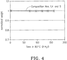
- FIGURE 4 is a graph that indicates that the weight loss measurements of the tested LLT glasses 202 (composition nos. 1 and 4-5).
- FIGURE 5 is a cross-sectional side view of an oven 502 which contains a device 200 that includes LLT glass films 202 (composition no. 1), two inner layers 204 (Al and Ca) and a substrate 206 (Corning Inc.'s 1737 glass substrate).
- the Al and Ca layers 204 were deposited on the thick substrate 206 and then encapsulated with LLT glass films 202 (composition no. 1).
- the "calcium patch” test was performed as follows. A 100 nm Ca film 204 was evaporated onto a Corning Inc.'s 1737 glass substrate 206. Then, a 200 nm Al layer 204 was evaporated on the Ca film 204. The Al layer 204 was used to simulate the conditions of a cathode typically used to produce polymer light emitting diodes (PLEDs). Using a "dual-boat" customized Cressington evaporator, the 1737 glass substrate 206 was maintained at 130°C and approximately 10 -6 Torr during the Ca and Al evaporation steps.
- PLEDs polymer light emitting diodes
- the LLT glass 202 (composition no. 1) was then sputtered onto the Al and Ca layers 204 under relatively gentle RF power deposition conditions (30 W forward/1 W reflected RF power) and low argon pressure ( ⁇ 19 sccm)(see step 102 in FIGURE 1 ). The sputtering was performed for 24 hours to obtain a glass thickness in the range of 2.5 ⁇ m (chamber pressure ⁇ 10 -3 Torr). It should be noted that the LLT material thickness can be made as thick as one needs depending on one's chosen deposition duration.
- FIGURE 6 shows the pictures of the tested devices 200 which were taken at regular intervals to follow the rate of calcium oxidation which is an indication of the permeation properties of the LTG glass films 202.
- the left panel in FIGURE 6 labeled "Typical Starting Condition" shows the initial metallic Ca layers 204 of tested devices 200 before oxidation reactions associated with this test occurred (i.e., Ca + 2H 2 O ⁇ Ca (OH) 2 + H 2 , and 2Ca + O 2 ⁇ 2CaO).
- the images in the bottom row were taken, at the indicated time intervals, of a sample device 200 prepared without any heating of the LLT glass sputtered glass layer 202.
- the images in the middle row were taken of a similar device 200 that was heated (at 121°C) during the first hour of the 24 hour glass deposition time interval. And, the tested device 200 shown in the top row was prepared similarly except that it was heated (at 121°C) after the 24 hour glass deposition time interval. Clearly, the tested device 200 shown in the top row that had the entire LTG glass thickness subjected to heat-treatment fended off oxygen and water attack best.
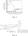
- FIGURE 7 is a graph that illustrates the percentage of calcium area oxidized due to time spent in the 85°C and 85% relative humidity oven 502 for the three tested devices 200 (see FIGURE 6 ) and one non-covered device.
- data 702 represents the percentage of the calcium patch surface area that was oxidized on a calcium patch that had the 100 nm calcium and 200 nm aluminum layers but was not coated with LLT glass 202.
- data 704 represents the calcium patch surface area that was oxidized in one of the tested devices 200 which had a 2.5 ⁇ m sputtered LLT glass layer 202 (composition no. 1) that was not heat treated.
- Data 706 represents the calcium patch surface area that was oxidized in another tested device 200 which had a 2.5 ⁇ m sputtered LLT glass layer 202 (composition no. 1) that was heat treated at 121°C for the first hour during the 24 hour deposition period.
- data 708 represents the calcium patch surface area that was oxidized in another test device 200 which had a 2.5 ⁇ m sputtered LLT glass layer 202 (composition no. 1) that was heat treated at 121°C for one hour after the 24 hour deposition period. As can be seen, the device 200 that was heat treated after the deposition period performed the best.
- the water permeation rate in the tested devices 200 were estimated by first calculating the total amount of calcium metal in the 100 nm layer 204. Then, by consulting FIGURE 7 and other additional data, we estimated the time it took for half the calcium in the 1.27cm (1 ⁇ 2") x 2.54cm (1") x 100 nm patch to become oxidized, the so-called half life. This yields the average number of grams oxidized with water vapor per day, per unit meter 2 in an 85/85 environment.
- FIGURES 9A and 9B These values may be illustrated graphically and compared with traditional seals like Vitex system's Barix TM seals as shown in FIGURES 9A and 9B .
- the data associated with the tested device 200 that had LLT glass 204 (composition no. 1) which was heat treated after the deposition step is shown in FIGURES 9A and 9B .
- the tested device 200 performed better than the device that used a Barix TM seal. It should be noted that the photograph/graph in FIGURE 9B also shows the relative levels of oxygen permeability of typical polymers and coatings and the sensitivity limits of current test equipment.
- LLT materials which have low liquidus temperatures to form a barrier layer with permeation properties comparable to the material itself.
- the LLT materials are tin fluorophosphate materials which include, but are not limited to, tin fluorophosphate glass. These LLT materials are especially suitable for inhibiting oxygen or/and moisture degradation common to electronic devices, food or medicine. In addition, these LLT materials may be used to reduce, for example, photochemical, hydrolytic, and oxidative damage due to chemically active permeants.
- the LLT materials are deposited by sputtering.
- Defects in the LLT materials from the deposition step are removed by a consolidation step (heat treatment) in order to produce a pore-free, gas and moisture impenetrable protective coating on the device.
- the barrier layer is quite durable, exhibiting low weight loss (0.28%) in standardized 1000 hour, 85°C water-immersion tests, and enduring over 600 hours in calcium patch tests, in 85°C and 85% relative humidity chambers.
- the consolidation step is truly practical with the LLT materials where the consolidation temperature is sufficiently low to inhibit thermal damage to nearby layers.
- the sputter-deposited thin film material is composed of 66% Sn 4+ and 34% Sn 2+ .
- Sn 4+ tetravalent tin
- barrier layers containing a subset of durable low liquidus temperature materials provide substantial protection from oxygen and water attack (and transport) beyond traditional physically-deposited oxide barrier layers.
- the preferred barrier layers described herein can have a water and oxygen permeance below 10 -6 g/m 2 /day and 10 -5 cc/m 2 /atm/day, respectively.
- physically-deposited low liquidus temperature thin-film barrier layers can be annealed at temperatures suitable for retaining the integrity of adjoining organic layer material physicochemical properties. This last feature makes durable low liquidus temperature materials unique compared with other physically deposited oxide barrier layers.
- low liquidus temperature materials can be annealed at a low temperature so as to remove mesoscopic defects from the physically deposited layers and also retain the physicochemical properties of the adjoining organic under-layers. This is in contrast to the Vitex TM method in which the defects are not removed. Moreover, it has been shown that these low liquidus temperature barrier layers can be used to form an integral part of various devices (e.g., waveguide, grating sensors, photonic crystals etc.) while inhibiting the transport of materials detrimental to high-performance operation.
- various devices e.g., waveguide, grating sensors, photonic crystals etc.
- tin fluorophosphate glass Even though specific types of tin fluorophosphate glass are discussed and described in detail herein, it should be appreciated that other types of tin fluorophosphate LLT materials may also be used in accordance with the present invention. It should also be appreciated that low liquidus temperature materials can be made which contain small-composite materials or other electro-optic dopants. These dopants can optimize the refractive indices or add additional electro-optic features to a device 200. This can be particularly, useful when the device 200 is a waveguide sensor.
Landscapes
- Chemical & Material Sciences (AREA)
- Materials Engineering (AREA)
- Engineering & Computer Science (AREA)
- Chemical Kinetics & Catalysis (AREA)
- General Chemical & Material Sciences (AREA)
- Geochemistry & Mineralogy (AREA)
- Life Sciences & Earth Sciences (AREA)
- Organic Chemistry (AREA)
- Physics & Mathematics (AREA)
- Optics & Photonics (AREA)
- Electroluminescent Light Sources (AREA)
- Physical Vapour Deposition (AREA)
- Glass Compositions (AREA)
- Laminated Bodies (AREA)
- Surface Treatment Of Glass (AREA)
Applications Claiming Priority (2)
| Application Number | Priority Date | Filing Date | Title |
|---|---|---|---|
| US11/207,691 US20070040501A1 (en) | 2005-08-18 | 2005-08-18 | Method for inhibiting oxygen and moisture degradation of a device and the resulting device |
| PCT/US2006/030670 WO2007021627A1 (en) | 2005-08-18 | 2006-08-09 | Method for inhibiting oxygen and moisture degradation of a device and the resulting device |
Publications (2)
| Publication Number | Publication Date |
|---|---|
| EP1929559A1 EP1929559A1 (en) | 2008-06-11 |
| EP1929559B1 true EP1929559B1 (en) | 2015-07-15 |
Family
ID=37460166
Family Applications (1)
| Application Number | Title | Priority Date | Filing Date |
|---|---|---|---|
| EP06800857.2A Ceased EP1929559B1 (en) | 2005-08-18 | 2006-08-09 | Method for inhibiting oxygen and moisture degradation of a device and the resulting device |
Country Status (7)
| Country | Link |
|---|---|
| US (2) | US20070040501A1 (enExample) |
| EP (1) | EP1929559B1 (enExample) |
| JP (1) | JP5113054B2 (enExample) |
| KR (1) | KR101353226B1 (enExample) |
| CN (1) | CN101243562A (enExample) |
| TW (1) | TWI360904B (enExample) |
| WO (1) | WO2007021627A1 (enExample) |
Cited By (1)
| Publication number | Priority date | Publication date | Assignee | Title |
|---|---|---|---|---|
| WO2017156048A1 (en) * | 2016-03-10 | 2017-09-14 | Corning Incorporated | Sealed devices comprising transparent laser weld regions |
Families Citing this family (54)
| Publication number | Priority date | Publication date | Assignee | Title |
|---|---|---|---|---|
| US20080206589A1 (en) * | 2007-02-28 | 2008-08-28 | Bruce Gardiner Aitken | Low tempertature sintering using Sn2+ containing inorganic materials to hermetically seal a device |
| US7722929B2 (en) | 2005-08-18 | 2010-05-25 | Corning Incorporated | Sealing technique for decreasing the time it takes to hermetically seal a device and the resulting hermetically sealed device |
| US7829147B2 (en) * | 2005-08-18 | 2010-11-09 | Corning Incorporated | Hermetically sealing a device without a heat treating step and the resulting hermetically sealed device |
| EP2180078B1 (en) * | 2005-08-25 | 2013-12-11 | Asahi Glass Company, Limited | Base with glass film |
| BRPI0714886B8 (pt) | 2006-07-10 | 2021-05-25 | Paion Uk Ltd | sais de benzodiazepina, seus usos e seus processos de preparação, e composição farmacêutica |
| US20080048178A1 (en) | 2006-08-24 | 2008-02-28 | Bruce Gardiner Aitken | Tin phosphate barrier film, method, and apparatus |
| EP2121872B1 (en) * | 2007-03-19 | 2015-12-09 | Nanosys, Inc. | Methods for encapsulating nanocrystals |
| US20100155749A1 (en) * | 2007-03-19 | 2010-06-24 | Nanosys, Inc. | Light-emitting diode (led) devices comprising nanocrystals |
| US20100110728A1 (en) | 2007-03-19 | 2010-05-06 | Nanosys, Inc. | Light-emitting diode (led) devices comprising nanocrystals |
| US20080290798A1 (en) * | 2007-05-22 | 2008-11-27 | Mark Alejandro Quesada | LLT barrier layer for top emission display device, method and apparatus |
| US8343575B2 (en) | 2008-12-30 | 2013-01-01 | Nanosys, Inc. | Methods for encapsulating nanocrystals and resulting compositions |
| US10214686B2 (en) | 2008-12-30 | 2019-02-26 | Nanosys, Inc. | Methods for encapsulating nanocrystals and resulting compositions |
| US11198270B2 (en) | 2008-12-30 | 2021-12-14 | Nanosys, Inc. | Quantum dot films, lighting devices, and lighting methods |
| US9799914B2 (en) | 2009-01-29 | 2017-10-24 | Corning Incorporated | Barrier layer for thin film battery |
| US8084380B2 (en) * | 2009-02-27 | 2011-12-27 | Corning Incorporated | Transition metal doped Sn phosphate glass |
| US8563113B2 (en) | 2010-04-20 | 2013-10-22 | Corning Incorporated | Multi-laminate hermetic barriers and related structures and methods of hermetic sealing |
| US20120028011A1 (en) | 2010-07-27 | 2012-02-02 | Chong Pyung An | Self-passivating mechanically stable hermetic thin film |
| US10158057B2 (en) | 2010-10-28 | 2018-12-18 | Corning Incorporated | LED lighting devices |
| EP2450039A1 (en) | 2010-11-08 | 2012-05-09 | PAION UK Ltd. | Dosing regimen for sedation with CNS 7056 (Remimazolam) |
| KR20200039806A (ko) | 2010-11-10 | 2020-04-16 | 나노시스, 인크. | 양자 도트 필름들, 조명 디바이스들, 및 조명 방법들 |
| KR101931177B1 (ko) * | 2012-03-02 | 2018-12-21 | 삼성디스플레이 주식회사 | 유기 발광 표시 장치 |
| KR101347541B1 (ko) * | 2012-03-02 | 2014-01-06 | 삼성디스플레이 주식회사 | 유기 발광 장치의 제조 방법 |
| KR101503401B1 (ko) * | 2012-03-05 | 2015-03-17 | 삼성디스플레이 주식회사 | 유기 발광 장치의 제조 방법 |
| KR101333138B1 (ko) | 2012-03-05 | 2013-11-26 | 삼성디스플레이 주식회사 | 유기 발광 장치의 제조 방법, 무기막 전사용 기판 및 유기 발광 장치 |
| KR102000709B1 (ko) * | 2012-08-31 | 2019-09-30 | 삼성디스플레이 주식회사 | 디스플레이 패널의 제조방법 |
| US10017849B2 (en) | 2012-11-29 | 2018-07-10 | Corning Incorporated | High rate deposition systems and processes for forming hermetic barrier layers |
| US9666763B2 (en) | 2012-11-30 | 2017-05-30 | Corning Incorporated | Glass sealing with transparent materials having transient absorption properties |
| KR101434367B1 (ko) | 2012-12-14 | 2014-08-27 | 삼성디스플레이 주식회사 | 유기 발광 표시 장치 및 그 제조방법 |
| JP6186377B2 (ja) | 2012-12-18 | 2017-08-23 | パイオニア株式会社 | 発光装置 |
| US8754434B1 (en) | 2013-01-28 | 2014-06-17 | Corning Incorporated | Flexible hermetic thin film with light extraction layer |
| AR094963A1 (es) | 2013-03-04 | 2015-09-09 | Ono Pharmaceutical Co | Reacción de oxidación excelente en el índice de conversión |
| KR20140120541A (ko) * | 2013-04-03 | 2014-10-14 | 삼성디스플레이 주식회사 | 유기 발광 표시 장치 및 그 제조 방법 |
| KR102072805B1 (ko) | 2013-04-15 | 2020-02-04 | 삼성디스플레이 주식회사 | 유기발광표시장치 및 그의 제조방법 |
| KR102072806B1 (ko) | 2013-04-18 | 2020-03-03 | 삼성디스플레이 주식회사 | 유기 발광 디스플레이 장치 및 이의 제조 방법 |
| KR101444065B1 (ko) | 2013-04-26 | 2014-09-26 | 삼성디스플레이 주식회사 | 유기 발광 표시 장치 및 그 제조 방법 |
| KR101563203B1 (ko) | 2013-04-30 | 2015-10-27 | 삼성디스플레이 주식회사 | 유기 발광 표시 장치 및 그 제조 방법 |
| CN105377783B (zh) | 2013-05-10 | 2019-03-08 | 康宁股份有限公司 | 采用低熔融玻璃或薄吸收膜对透明玻璃片进行激光焊接 |
| KR102093391B1 (ko) | 2013-07-12 | 2020-03-26 | 삼성디스플레이 주식회사 | 유기 발광 표시 장치 및 그 제조 방법 |
| KR20150007865A (ko) | 2013-07-12 | 2015-01-21 | 삼성디스플레이 주식회사 | 스퍼터링 타겟의 제조 방법, 그 방법으로 제조된 스퍼터링 타겟 및 그 스퍼터링 타겟을 이용하여 유기 발광 표시 장치를 제조하는 방법 |
| KR102093392B1 (ko) | 2013-07-25 | 2020-03-26 | 삼성디스플레이 주식회사 | 유기 발광 표시 장치 및 유기 발광 표시 장치 제조 방법 |
| KR102096053B1 (ko) | 2013-07-25 | 2020-04-02 | 삼성디스플레이 주식회사 | 유기발광표시장치의 제조방법 |
| KR20150012540A (ko) * | 2013-07-25 | 2015-02-04 | 삼성디스플레이 주식회사 | 유기발광표시장치의 제조방법. |
| KR102120896B1 (ko) | 2013-07-25 | 2020-06-10 | 삼성디스플레이 주식회사 | 대향 타겟 스퍼터링 장치를 이용한 유기발광표시장치 및 그 제조방법 |
| KR102085319B1 (ko) * | 2013-07-30 | 2020-03-06 | 삼성디스플레이 주식회사 | 유기 발광 디스플레이 장치 및 이의 제조 방법 |
| KR20150016780A (ko) | 2013-08-05 | 2015-02-13 | 삼성디스플레이 주식회사 | 유기 발광 표시 장치 및 그 제조 방법 |
| KR20150143966A (ko) | 2014-06-13 | 2015-12-24 | 삼성디스플레이 주식회사 | 표시 장치 제조 방법 |
| KR102278605B1 (ko) | 2014-09-25 | 2021-07-19 | 삼성디스플레이 주식회사 | 저온 점도변화 조성물, 표시 장치 및 이의 제조 방법 |
| CN105336878A (zh) * | 2015-09-29 | 2016-02-17 | 北京维信诺光电技术有限公司 | 一种oled显示器件及其封装工艺 |
| US10647608B2 (en) * | 2016-01-08 | 2020-05-12 | Yej Glass Co., Ltd. | Fluorinated tin-based glass frit and method for manufacturing same |
| KR20190069840A (ko) | 2017-12-12 | 2019-06-20 | 이수후 | 풀 용기 |
| CN109994643B (zh) | 2018-01-02 | 2021-02-02 | 京东方科技集团股份有限公司 | 有机发光二极管器件及其制造方法、显示基板、显示装置 |
| US10811330B1 (en) | 2018-02-02 | 2020-10-20 | Verily Life Sciences Llc | Miniaturized electronic devices and related methods |
| CN109390498A (zh) * | 2018-11-29 | 2019-02-26 | 云谷(固安)科技有限公司 | 显示面板及其制备方法 |
| KR200493125Y1 (ko) | 2020-03-16 | 2021-02-03 | 이수후 | 풀 용기 |
Family Cites Families (211)
| Publication number | Priority date | Publication date | Assignee | Title |
|---|---|---|---|---|
| US1615506A (en) | 1925-12-08 | 1927-01-25 | George G Felt | Cap attachment for fountain pens |
| US3622439A (en) | 1968-05-23 | 1971-11-23 | Tee Pak Inc | Oxygen impermeable film laminate |
| US3932693A (en) | 1970-10-19 | 1976-01-13 | Continental Can Company, Inc. | Laminated packaging film having low vapor and gas permeability |
| US3720097A (en) * | 1971-01-21 | 1973-03-13 | Univ Pennsylvania | Apparatus and method for measuring mammalian blood viscosity |
| US3795976A (en) * | 1972-10-16 | 1974-03-12 | Hitachi Ltd | Method of producing semiconductor device |
| US3828960A (en) | 1972-11-10 | 1974-08-13 | Dow Chemical Co | Heat insulating container having plastic walls retaining vacuum |
| DE2431917A1 (de) * | 1974-07-03 | 1976-01-22 | Bbc Brown Boveri & Cie | Glaspassiviertes halbleiterbauelement fuer hohe leistungen und verfahren zu seiner herstellung |
| US4040874A (en) * | 1975-08-04 | 1977-08-09 | General Electric Company | Semiconductor element having a polymeric protective coating and glass coating overlay |
| US4077588A (en) | 1975-09-15 | 1978-03-07 | Hurst Gerald L | Permanently buoyant balloon |
| JPS5626395A (en) * | 1979-08-10 | 1981-03-13 | Fujitsu Ltd | El display unit |
| US4314031A (en) * | 1980-06-17 | 1982-02-02 | Corning Glass Works | Tin-phosphorus oxyfluoride glasses |
| US4374391A (en) | 1980-09-24 | 1983-02-15 | Bell Telephone Laboratories, Incorporated | Device fabrication procedure |
| US4702963A (en) | 1981-04-03 | 1987-10-27 | Optical Coating Laboratory, Inc. | Flexible polymer film with vapor impermeable coating |
| DE3201482A1 (de) | 1982-01-20 | 1983-09-08 | Bayer Ag, 5090 Leverkusen | Mehrschichten-flaechengebilde |
| US4379070A (en) * | 1982-04-26 | 1983-04-05 | Corning Glass Works | Tin-phosphorus oxyfluoride glass containing aromatic organic compound |
| DE3334845A1 (de) | 1983-09-27 | 1985-04-11 | Dow Chemical Handels- und Vertriebsgesellschaft mbH, 2610 Stade | Ueberzugszusammensetzung und ihre verwendung zur herstellung von sauerstoffdichten beschichtungen auf kunststoffgegenstaenden |
| JPS60161146A (ja) | 1984-01-31 | 1985-08-22 | 株式会社クラレ | 耐屈曲疲労に優れたフレキシブルな気体遮断性積層包装材よりなるバッグインボックス内容器の構成材 |
| FI73923C (fi) | 1985-11-27 | 1991-01-01 | Wihuri Oy | Polyamidhaltig maongskiktsfilm. |
| JP2632673B2 (ja) | 1986-09-14 | 1997-07-23 | 東洋紡績 株式会社 | 液晶表示パネル用電極基板 |
| US4908272A (en) | 1987-04-27 | 1990-03-13 | Mitsubishi Gas Chemical Company, Inc. | Gas-barrier multilayered structure |
| AU616736B2 (en) | 1988-03-03 | 1991-11-07 | Asahi Glass Company Limited | Amorphous oxide film and article having such film thereon |
| US4859513A (en) | 1988-05-09 | 1989-08-22 | International Paper Company | Oxygen impermeable leak free container |
| EP0394519B1 (en) | 1989-04-26 | 1994-02-02 | Fujimori Kogyo Co., Ltd. | Liquid crystal display panel incorporating an optical phase shifting substrate |
| CA2027031A1 (en) * | 1989-10-18 | 1991-04-19 | Loren A. Haluska | Hermetic substrate coatings in an inert gas atmosphere |
| US5792550A (en) | 1989-10-24 | 1998-08-11 | Flex Products, Inc. | Barrier film having high colorless transparency and method |
| US5183684A (en) | 1989-11-20 | 1993-02-02 | Dow Corning Corporation | Single and multilayer coatings containing aluminum nitride |
| JP2936276B2 (ja) * | 1990-02-27 | 1999-08-23 | 日本真空技術株式会社 | 透明導電膜の製造方法およびその製造装置 |
| US5084356A (en) | 1990-04-20 | 1992-01-28 | E. I. Du Pont De Nemours And Company | Film coated with glass barrier layer with metal dopant |
| US6524698B1 (en) | 1990-09-27 | 2003-02-25 | Helmuth Schmoock | Fluid impermeable foil |
| US5089446A (en) | 1990-10-09 | 1992-02-18 | Corning Incorporated | Sealing materials and glasses |
| US5110668A (en) | 1990-12-21 | 1992-05-05 | General Electric Company | Flexible laminate having copolyetherester adhesive |
| SE468635B (sv) | 1991-01-09 | 1993-02-22 | Tetra Alfa Holdings | Foerpackningsmaterial jaemte anvaendning av materialet foer framstaellning av behaallare med goda syrgastaethetsegenskaper |
| SE502397C2 (sv) | 1991-05-03 | 1995-10-16 | Tetra Laval Holdings & Finance | Förpackningslaminat med goda förseglings- och barriäregenskaper samt av förpackningslaminatet framställda förpackningsbehållare |
| DE4123127C2 (de) | 1991-07-12 | 1996-06-20 | Hoechst Ag | Mehrschichtenverbundfolie mit verbesserter Gasbarrierewirkung |
| JP3158667B2 (ja) | 1991-08-01 | 2001-04-23 | セイコーエプソン株式会社 | 液晶表示素子の製造方法及び液晶表示素子の再生方法 |
| US5211995A (en) | 1991-09-30 | 1993-05-18 | Manfred R. Kuehnle | Method of protecting an organic surface by deposition of an inorganic refractory coating thereon |
| CA2123809A1 (en) | 1991-12-18 | 1993-06-24 | Debra L. Wilfong | Multilayered barrier structures |
| US5306533A (en) | 1992-04-27 | 1994-04-26 | Combibloc, Inc. | Oxygen barrier container |
| NZ248674A (en) | 1992-09-18 | 1996-03-26 | Grace W R & Co | Heat-shrinkable multilayer film comprising a layer of propylene polymer or copolymer and hydrocarbon resin, and outer layers of various other polymers |
| US5462779A (en) | 1992-10-02 | 1995-10-31 | Consorzio Ce.Te.V. Centro Tecnologie Del Vuoto | Thin film multilayer structure as permeation barrier on plastic film |
| US5641559A (en) | 1992-10-23 | 1997-06-24 | Toyo Seikan Kaisha, Ltd. | Gas-tight laminated plastic film containing polymer of organosilicic compound |
| EP0638939A3 (en) | 1993-07-19 | 1997-08-20 | Matsushita Electric Industrial Co Ltd | Solar cell with a layer of glass with a low melting point. |
| US5567488A (en) | 1993-09-16 | 1996-10-22 | The Dow Chemical Company | Multilayer barrier film for transdermal drug delivery system and ostomy applications |
| EP0646611B1 (en) | 1993-09-30 | 1999-01-27 | Toppan Printing Co., Ltd. | Gas barrier laminated material |
| US6403176B1 (en) | 1993-12-08 | 2002-06-11 | Andre Patouraux | Packaging laminate for bags |
| US5668663A (en) * | 1994-05-05 | 1997-09-16 | Donnelly Corporation | Electrochromic mirrors and devices |
| US5625729A (en) | 1994-08-12 | 1997-04-29 | Brown; Thomas G. | Optoelectronic device for coupling between an external optical wave and a local optical wave for optical modulators and detectors |
| EP0701897B1 (en) | 1994-09-16 | 2001-04-18 | Cryovac, Inc. | Thermoplastic multilayer film for use in packaging water |
| EP0705757A1 (en) | 1994-10-07 | 1996-04-10 | Rhone-Poulenc Inc. | Lighter than air balloons |
| DE4438359C2 (de) | 1994-10-27 | 2001-10-04 | Schott Glas | Behälter aus Kunststoff mit einer Sperrbeschichtung |
| DE69630829T2 (de) | 1995-02-02 | 2004-09-23 | Teijin Ltd. | Transparentes leitfähiges Flächenmaterial |
| EP0744285B1 (en) | 1995-05-24 | 1999-12-15 | Cryovac, Inc. | Multilayer oxygen barrier packaging film |
| US6211560B1 (en) * | 1995-06-16 | 2001-04-03 | The United States Of America As Represented By The Secretary Of The Air Force | Voltage tunable schottky diode photoemissive infrared detector |
| EP0868363B1 (en) | 1995-12-20 | 2003-11-26 | Tetra Laval Holdings & Finance SA | Method of producing a laminated packaging material |
| TW434301B (en) | 1996-01-30 | 2001-05-16 | Becton Dickinson Co | Non-ideal barrier coating composition comprising organic and inorganic materials |
| CA2200829C (en) | 1996-03-25 | 2006-02-21 | Toru Hanada | Liquid crystal display element with a transparent electrode substrate, and the transparent electrode substrate |
| GB2318680B (en) * | 1996-10-24 | 2001-11-07 | Univ Surrey | Optoelectronic semiconductor devices |
| US6294420B1 (en) * | 1997-01-31 | 2001-09-25 | Texas Instruments Incorporated | Integrated circuit capacitor |
| FR2759755B1 (fr) | 1997-02-17 | 1999-04-02 | Atochem Elf Sa | Membrane elastique impermeable aux gaz et accumulateur hydropneumatique equipe de cette membrane |
| JP3334558B2 (ja) * | 1997-04-23 | 2002-10-15 | 富士レビオ株式会社 | 酵素免疫測定方法及び試験片 |
| US6074717A (en) | 1997-07-29 | 2000-06-13 | Dayco Products, Inc. | Flexible hose having an aluminum barrier layer to prevent ingestion of oxygen |
| JP3900617B2 (ja) * | 1997-09-17 | 2007-04-04 | カシオ計算機株式会社 | 発光素子及び発光素子用の保護材料 |
| JP3906325B2 (ja) | 1997-10-09 | 2007-04-18 | テトラ ラバル ホールデイングス アンド ファイナンス エス エイ | 気体及び芳香バリア特性を備える包装積層体 |
| KR100247935B1 (ko) * | 1997-10-22 | 2000-03-15 | 윤종용 | 오산화 이탄탈륨 유전체막을 갖는 커패시터 형성방법 |
| KR19990061716A (ko) * | 1997-12-31 | 1999-07-26 | 윤종용 | 비스(디알킬말레이미드) 유도체 및 이로부터 형성된 광통신용 폴리에테르이미드 |
| JP3636914B2 (ja) * | 1998-02-16 | 2005-04-06 | 株式会社日鉱マテリアルズ | 高抵抗透明導電膜及び高抵抗透明導電膜の製造方法並びに高抵抗透明導電膜形成用スパッタリングターゲット |
| JP3845853B2 (ja) * | 1998-04-06 | 2006-11-15 | 日本電気硝子株式会社 | ホウリン酸スズ系ガラス及び封着材料 |
| US6465101B1 (en) | 1998-04-28 | 2002-10-15 | General Electric Company | Multilayer plastic articles |
| US6683094B2 (en) * | 1998-07-02 | 2004-01-27 | Aventis Pharmaceuticals Inc. | Antihistaminic piperidine derivatives and intermediates for the preparation thereof |
| WO2000005069A1 (en) | 1998-07-24 | 2000-02-03 | Japan Polyolefins Co., Ltd. | Gas barrier laminate, process for producing the same, and paper container made using the laminate |
| US6146225A (en) | 1998-07-30 | 2000-11-14 | Agilent Technologies, Inc. | Transparent, flexible permeability barrier for organic electroluminescent devices |
| US6635989B1 (en) * | 1998-08-03 | 2003-10-21 | E. I. Du Pont De Nemours And Company | Encapsulation of polymer-based solid state devices with inorganic materials |
| JP2000109726A (ja) | 1998-09-30 | 2000-04-18 | Dow Corning Toray Silicone Co Ltd | ガスバリア用組成物および樹脂成形体 |
| US6249014B1 (en) * | 1998-10-01 | 2001-06-19 | Ramtron International Corporation | Hydrogen barrier encapsulation techniques for the control of hydrogen induced degradation of ferroelectric capacitors in conjunction with multilevel metal processing for non-volatile integrated circuit memory devices |
| JP3802244B2 (ja) | 1998-10-02 | 2006-07-26 | 三洋化成工業株式会社 | 燃料油用清浄剤及び燃料油組成物 |
| US6271150B1 (en) | 1998-11-30 | 2001-08-07 | North Carolina State University | Methods of raising reflow temperature of glass alloys by thermal treatment in steam, and microelectronic structures formed thereby |
| US6268695B1 (en) * | 1998-12-16 | 2001-07-31 | Battelle Memorial Institute | Environmental barrier material for organic light emitting device and method of making |
| US6321571B1 (en) * | 1998-12-21 | 2001-11-27 | Corning Incorporated | Method of making glass structures for flat panel displays |
| DE19920002A1 (de) | 1999-05-03 | 2000-11-09 | Sms Demag Ag | Gichtverschluß für Schachtöfen, insbesondere Hochöfen mit einem Guteinlauftrichter |
| US6355125B1 (en) * | 1999-03-26 | 2002-03-12 | Agfa-Gevaert | Method for making an electric or electronic module comprising a glass laminate |
| HUP0200536A2 (en) * | 1999-04-28 | 2002-06-29 | Du Pont | Electroluminescent display, photo sensor and method for improving oxygen and moisture resistance of an organic electronic device |
| EP1060875A3 (de) | 1999-06-15 | 2001-12-12 | Alcan Technology & Management AG | Sterilisierbare Verbundfolie |
| JP4950400B2 (ja) | 1999-07-09 | 2012-06-13 | インスティチュート オブ マテリアルズ リサーチ アンド エンジニアリング | デバイスを封入するためのラミネート |
| US6083313A (en) | 1999-07-27 | 2000-07-04 | Advanced Refractory Technologies, Inc. | Hardcoats for flat panel display substrates |
| JP3951514B2 (ja) | 1999-08-11 | 2007-08-01 | 日本電気硝子株式会社 | シリカリン酸スズ系ガラス及び封着材料 |
| US6660409B1 (en) | 1999-09-16 | 2003-12-09 | Panasonic Communications Co., Ltd | Electronic device and process for producing the same |
| TW432689B (en) * | 1999-10-18 | 2001-05-01 | Taiwan Semiconductor Mfg | Fabricating method of stacked capacitor |
| US6413645B1 (en) * | 2000-04-20 | 2002-07-02 | Battelle Memorial Institute | Ultrabarrier substrates |
| US6866901B2 (en) * | 1999-10-25 | 2005-03-15 | Vitex Systems, Inc. | Method for edge sealing barrier films |
| US6623861B2 (en) | 2001-04-16 | 2003-09-23 | Battelle Memorial Institute | Multilayer plastic substrates |
| US7198832B2 (en) | 1999-10-25 | 2007-04-03 | Vitex Systems, Inc. | Method for edge sealing barrier films |
| EP1096568A3 (en) * | 1999-10-28 | 2007-10-24 | Sony Corporation | Display apparatus and method for fabricating the same |
| US6244441B1 (en) | 1999-11-10 | 2001-06-12 | Cryovac, Inc. | Heat sealable barrier film for fluid fillable packaging cushions and cushions made therefrom |
| US6530477B1 (en) | 1999-11-10 | 2003-03-11 | Joseph G. Martorano | Flexible packaging for maintaining the efficacy of chemicals |
| US6961490B2 (en) * | 2000-01-27 | 2005-11-01 | Unaxis-Balzers Aktiengesellschaft | Waveguide plate and process for its production and microtitre plate |
| JP3536763B2 (ja) * | 2000-02-04 | 2004-06-14 | 日本電気株式会社 | 封止装置 |
| WO2001065167A1 (en) | 2000-03-02 | 2001-09-07 | Pearl Technology Holdings, Llc | Inflatable structure for supporting an article of manufacture |
| US20010038894A1 (en) * | 2000-03-14 | 2001-11-08 | Minoru Komada | Gas barrier film |
| US6805998B2 (en) | 2000-03-24 | 2004-10-19 | Cymbet Corporation | Method and apparatus for integrated-battery devices |
| US6777871B2 (en) * | 2000-03-31 | 2004-08-17 | General Electric Company | Organic electroluminescent devices with enhanced light extraction |
| US6657232B2 (en) * | 2000-04-17 | 2003-12-02 | Virginia Commonwealth University | Defect reduction in GaN and related materials |
| US6492026B1 (en) | 2000-04-20 | 2002-12-10 | Battelle Memorial Institute | Smoothing and barrier layers on high Tg substrates |
| US6870207B2 (en) * | 2000-04-24 | 2005-03-22 | The University Of Connecticut | III-V charge coupled device suitable for visible, near and far infra-red detection |
| AU2001259540A1 (en) | 2000-05-04 | 2001-11-12 | Pearl Technology Holdings, Llc | Inflatable organic light emitting diode toys |
| US6193379B1 (en) * | 2000-06-09 | 2001-02-27 | Gentex Corporation | Electrochromic assembly including at least one polymeric substrate |
| AU5400501A (en) | 2000-06-27 | 2002-01-03 | Canon Kabushiki Kaisha | Photovoltaic element, producing method therefor, and solar cell modules |
| DE10039366A1 (de) | 2000-08-11 | 2002-02-21 | Mitsubishi Polyester Film Gmbh | Mindestens dreischichtige transparente Polyesterfolie, Verfahren zu ihrer Herstellung und ihre Verwendung |
| DE10047043A1 (de) | 2000-09-22 | 2002-04-11 | Wolff Walsrode Ag | Folienlaminate als Hochbarrierefolien und deren Verwendung in Vakuumisolierpaneelen |
| JP2002187231A (ja) * | 2000-10-13 | 2002-07-02 | Dainippon Printing Co Ltd | バリア性フィルムおよびその製造法 |
| US7142296B2 (en) * | 2000-10-30 | 2006-11-28 | Sru Biosystems, Inc. | Method and apparatus for detecting biomolecular interactions |
| US6503421B1 (en) | 2000-11-01 | 2003-01-07 | Corning Incorporated | All polymer process compatible optical polymer material |
| EP1207572A1 (en) | 2000-11-15 | 2002-05-22 | Dr. Sugnaux Consulting | Mesoporous electrodes for electrochemical cells and their production method |
| JP4848583B2 (ja) | 2000-11-21 | 2011-12-28 | 大日本印刷株式会社 | ハードコート層を有するフィルムの製造方法 |
| EP1401731A2 (en) | 2000-11-29 | 2004-03-31 | American Aerogel Corporation | Insulated barriers and methods for producing same |
| US6608360B2 (en) * | 2000-12-15 | 2003-08-19 | University Of Houston | One-chip micro-integrated optoelectronic sensor |
| US6461681B2 (en) * | 2001-01-08 | 2002-10-08 | Hewlett-Packard Company | Method of treating a surface of a polyimide |
| JP4272819B2 (ja) | 2001-01-10 | 2009-06-03 | キヤノン株式会社 | 有機発光素子 |
| EP1409584B1 (en) * | 2001-02-13 | 2010-01-20 | GLS Corporation | Removable seal of essentially gas-impermeable thermoplastic elastomer |
| US6849171B2 (en) * | 2001-03-05 | 2005-02-01 | Fuji Xerox Co., Ltd. | Light waveguide forming method, electrolyte solution, light waveguide forming apparatus and light waveguide |
| US6664137B2 (en) * | 2001-03-29 | 2003-12-16 | Universal Display Corporation | Methods and structures for reducing lateral diffusion through cooperative barrier layers |
| US6630980B2 (en) | 2001-04-17 | 2003-10-07 | General Electric Company | Transparent flexible barrier for liquid crystal display devices and method of making the same |
| US6864435B2 (en) | 2001-04-25 | 2005-03-08 | Alien Technology Corporation | Electrical contacts for flexible displays |
| US6774300B2 (en) * | 2001-04-27 | 2004-08-10 | Adrena, Inc. | Apparatus and method for photovoltaic energy production based on internal charge emission in a solid-state heterostructure |
| WO2002091064A2 (en) | 2001-05-04 | 2002-11-14 | General Atomics | O2 and h2o barrier material |
| TW570876B (en) | 2001-05-11 | 2004-01-11 | Toyo Seikan Kaisha Ltd | Silicon oxide film |
| JP3678361B2 (ja) * | 2001-06-08 | 2005-08-03 | 大日本印刷株式会社 | ガスバリアフィルム |
| DE10130666A1 (de) | 2001-06-28 | 2003-01-23 | Applied Films Gmbh & Co Kg | Softcoat |
| CA2352567A1 (en) | 2001-07-06 | 2003-01-06 | Mohamed Latreche | Translucent material displaying ultra-low transport of gases and vapors, and method for its production |
| JP2003020235A (ja) | 2001-07-06 | 2003-01-24 | Otsuka Ohmi Ceramics Co Ltd | 立体模様付きガラス板の製造方法 |
| US6664730B2 (en) * | 2001-07-09 | 2003-12-16 | Universal Display Corporation | Electrode structure of el device |
| FI117622B (fi) | 2001-07-13 | 2006-12-29 | Stora Enso Oyj | Polymeeripinnoitteinen kuumasaumattava pakkausmateriaali, sen valmistusmenetelmä sekä sen käyttö suljettuun pakkaukseen |
| KR100413450B1 (ko) * | 2001-07-20 | 2003-12-31 | 엘지전자 주식회사 | 표시소자의 보호막 구조 |
| CN1317421C (zh) | 2001-08-20 | 2007-05-23 | 诺华等离子公司 | 气体和蒸气低渗透性的涂层 |
| US6806145B2 (en) * | 2001-08-31 | 2004-10-19 | Asm International, N.V. | Low temperature method of forming a gate stack with a high k layer deposited over an interfacial oxide layer |
| US6734370B2 (en) | 2001-09-07 | 2004-05-11 | Irvine Sensors Corporation | Multilayer modules with flexible substrates |
| TW508808B (en) * | 2001-09-14 | 2002-11-01 | Winbond Electronics Corp | Stacked type capacitor structure and its manufacturing method |
| JP2003109775A (ja) * | 2001-09-28 | 2003-04-11 | Sony Corp | 有機電界発光素子 |
| FR2830206B1 (fr) | 2001-09-28 | 2004-07-23 | Corning Inc | Dispositif microfluidique et sa fabrication |
| JP2003128720A (ja) | 2001-10-19 | 2003-05-08 | Sunallomer Ltd | オレフィン重合用固体助触媒成分、オレフィン重合用触媒およびイオン含有化合物 |
| KR100768182B1 (ko) * | 2001-10-26 | 2007-10-17 | 삼성에스디아이 주식회사 | 유기 전자 발광 소자와 그 제조방법 |
| US6888305B2 (en) * | 2001-11-06 | 2005-05-03 | Universal Display Corporation | Encapsulation structure that acts as a multilayer mirror |
| JP2003142579A (ja) * | 2001-11-07 | 2003-05-16 | Hitachi Ltd | 半導体装置の製造方法および半導体装置 |
| US6486549B1 (en) * | 2001-11-10 | 2002-11-26 | Bridge Semiconductor Corporation | Semiconductor module with encapsulant base |
| SG114514A1 (en) | 2001-11-28 | 2005-09-28 | Univ Singapore | Organic light emitting diode (oled) |
| JP2005513738A (ja) * | 2001-12-20 | 2005-05-12 | アイファイア テクノロジー コーポレーション | エレクトロルミネセンスディスプレイの安定化電極 |
| US6936131B2 (en) * | 2002-01-31 | 2005-08-30 | 3M Innovative Properties Company | Encapsulation of organic electronic devices using adsorbent loaded adhesives |
| KR100845557B1 (ko) * | 2002-02-20 | 2008-07-10 | 삼성전자주식회사 | 액티브 매트릭스형 유기전계발광 표시장치 및 그 제조방법 |
| US6876143B2 (en) * | 2002-11-19 | 2005-04-05 | John James Daniels | Organic light active devices and methods for fabricating the same |
| JP2003275575A (ja) | 2002-03-22 | 2003-09-30 | Nippon Sheet Glass Co Ltd | マイクロ化学システム用チップ部材のチャネル形成方法、及び該形成方法によってチャネルが形成されたマイクロ化学システム用チップ部材 |
| US6891330B2 (en) * | 2002-03-29 | 2005-05-10 | General Electric Company | Mechanically flexible organic electroluminescent device with directional light emission |
| US20030183915A1 (en) | 2002-04-02 | 2003-10-02 | Motorola, Inc. | Encapsulated organic semiconductor device and method |
| US20030188685A1 (en) | 2002-04-08 | 2003-10-09 | Applied Materials, Inc. | Laser drilled surfaces for substrate processing chambers |
| KR100537611B1 (ko) * | 2002-04-10 | 2005-12-19 | 삼성에스디아이 주식회사 | 유기 전계 발광소자 및 그 제조방법 |
| US6835950B2 (en) * | 2002-04-12 | 2004-12-28 | Universal Display Corporation | Organic electronic devices with pressure sensitive adhesive layer |
| US7268486B2 (en) * | 2002-04-15 | 2007-09-11 | Schott Ag | Hermetic encapsulation of organic, electro-optical elements |
| US20030203210A1 (en) * | 2002-04-30 | 2003-10-30 | Vitex Systems, Inc. | Barrier coatings and methods of making same |
| US6949389B2 (en) * | 2002-05-02 | 2005-09-27 | Osram Opto Semiconductors Gmbh | Encapsulation for organic light emitting diodes devices |
| US6655788B1 (en) * | 2002-05-17 | 2003-12-02 | Viztec Inc. | Composite structure for enhanced flexibility of electro-optic displays with sliding layers |
| US6743524B2 (en) | 2002-05-23 | 2004-06-01 | General Electric Company | Barrier layer for an article and method of making said barrier layer by expanding thermal plasma |
| JP2004010843A (ja) | 2002-06-11 | 2004-01-15 | Idemitsu Petrochem Co Ltd | ポリ乳酸樹脂組成物 |
| US20040033379A1 (en) | 2002-06-12 | 2004-02-19 | Avery Dennison Corporation | Low permeability materials and coatings |
| JP4093347B2 (ja) | 2002-06-19 | 2008-06-04 | Agcテクノグラス株式会社 | 点火プラグ用封着ガラスおよび点火プラグ |
| JP4045870B2 (ja) | 2002-06-20 | 2008-02-13 | 富士ゼロックス株式会社 | 光学素子作製方法、これに用いる電着液および光学素子製造装置 |
| US7107592B2 (en) * | 2002-07-25 | 2006-09-12 | Sun Microsystems, Inc. | Method, system, and program for making objects available for access to a client over a network |
| US20040043138A1 (en) | 2002-08-21 | 2004-03-04 | Ramesh Jagannathan | Solid state lighting using compressed fluid coatings |
| JP2004095953A (ja) * | 2002-09-02 | 2004-03-25 | Canon Inc | 窒化シリコンの堆積膜形成方法 |
| FR2843899A1 (fr) * | 2002-09-03 | 2004-03-05 | Corning Inc | Depot d'un film sur un substrat |
| US7224116B2 (en) * | 2002-09-11 | 2007-05-29 | Osram Opto Semiconductors Gmbh | Encapsulation of active electronic devices |
| US20040229051A1 (en) | 2003-05-15 | 2004-11-18 | General Electric Company | Multilayer coating package on flexible substrates for electro-optical devices |
| US7015640B2 (en) * | 2002-09-11 | 2006-03-21 | General Electric Company | Diffusion barrier coatings having graded compositions and devices incorporating the same |
| US7193364B2 (en) * | 2002-09-12 | 2007-03-20 | Osram Opto Semiconductors (Malaysia) Sdn. Bhd | Encapsulation for organic devices |
| JP2004111059A (ja) * | 2002-09-13 | 2004-04-08 | Sony Corp | 表示装置 |
| GB2421117B (en) * | 2002-09-17 | 2006-09-27 | Dainippon Printing Co Ltd | Method of manufacturing a light emitting display panel and a light emitting diplay panel |
| US7138293B2 (en) * | 2002-10-04 | 2006-11-21 | Dalsa Semiconductor Inc. | Wafer level packaging technique for microdevices |
| ITMI20022159A1 (it) | 2002-10-11 | 2004-04-12 | Tecno Coating Engineering S R L | Pellicola multistrato termoretraibile avente barriera all'ossigeno ed al vapore acqueo, una migliorata resistenza meccanica e buone caratteristiche ottiche e ridotto effetto curling. |
| US7015639B2 (en) * | 2002-10-22 | 2006-03-21 | Osram Opto Semiconductors Gmbh | Electroluminescent devices and method of making transparent cathodes |
| US6878620B2 (en) * | 2002-11-12 | 2005-04-12 | Applied Materials, Inc. | Side wall passivation films for damascene cu/low k electronic devices |
| DK1420041T3 (da) | 2002-11-18 | 2010-08-09 | Icopal As | Fleksibelt foliemateriale |
| US7256427B2 (en) * | 2002-11-19 | 2007-08-14 | Articulated Technologies, Llc | Organic light active devices with particulated light active material in a carrier matrix |
| KR20050065680A (ko) | 2002-11-19 | 2005-06-29 | 다니엘즈 존 | 유기 및 무기 광 활성 장치들 |
| US20040100176A1 (en) * | 2002-11-21 | 2004-05-27 | Osram Opto Semiconductors Gmbh | Organic electronic device that filters colors |
| DE10256629B3 (de) * | 2002-12-03 | 2004-02-19 | Schott Glas | Vorzugsweise Pb- und As-freie optische Gläser mit Tg ≦ 500°C und deren Verwendung |
| US7086918B2 (en) * | 2002-12-11 | 2006-08-08 | Applied Materials, Inc. | Low temperature process for passivation applications |
| US6975067B2 (en) * | 2002-12-19 | 2005-12-13 | 3M Innovative Properties Company | Organic electroluminescent device and encapsulation method |
| US6787453B2 (en) * | 2002-12-23 | 2004-09-07 | Intel Corporation | Barrier film integrity on porous low k dielectrics by application of a hydrocarbon plasma treatment |
| US7372069B2 (en) * | 2003-01-14 | 2008-05-13 | Osram Opto Semiconductors Gmbh | Interface for UV-curable adhesives |
| US20040151934A1 (en) * | 2003-01-27 | 2004-08-05 | Schwark Dwight W. | Oxygen scavenging film with high slip properties |
| US20040157426A1 (en) * | 2003-02-07 | 2004-08-12 | Luc Ouellet | Fabrication of advanced silicon-based MEMS devices |
| JP4255844B2 (ja) * | 2003-02-24 | 2009-04-15 | ソニー株式会社 | 有機発光表示装置およびその製造方法 |
| JP2006519473A (ja) | 2003-03-04 | 2006-08-24 | ダウ・コーニング・コーポレイション | 有機発光ダイオード |
| EP1466997B1 (en) * | 2003-03-10 | 2012-02-22 | OSRAM Opto Semiconductors GmbH | Method for forming and arrangement of barrier layers on a polymeric substrate |
| US7018713B2 (en) * | 2003-04-02 | 2006-03-28 | 3M Innovative Properties Company | Flexible high-temperature ultrabarrier |
| US7514149B2 (en) | 2003-04-04 | 2009-04-07 | Corning Incorporated | High-strength laminated sheet for optical applications |
| US7202602B2 (en) * | 2003-04-08 | 2007-04-10 | Organic Lighting Technologies Llc | Metal seal packaging for organic light emitting diode device |
| US6888172B2 (en) * | 2003-04-11 | 2005-05-03 | Eastman Kodak Company | Apparatus and method for encapsulating an OLED formed on a flexible substrate |
| US20040206953A1 (en) * | 2003-04-16 | 2004-10-21 | Robert Morena | Hermetically sealed glass package and method of fabrication |
| US6998776B2 (en) * | 2003-04-16 | 2006-02-14 | Corning Incorporated | Glass package that is hermetically sealed with a frit and method of fabrication |
| CN1791989A (zh) | 2003-05-16 | 2006-06-21 | 纳幕尔杜邦公司 | 通过原子层沉积形成的塑料基材阻挡层膜 |
| US20040234797A1 (en) | 2003-05-23 | 2004-11-25 | Cryovac, Inc. | Oxygen scavenging film with antifog properties |
| US7535017B2 (en) | 2003-05-30 | 2009-05-19 | Osram Opto Semiconductors Gmbh | Flexible multilayer packaging material and electronic devices with the packaging material |
| US20050051763A1 (en) | 2003-09-05 | 2005-03-10 | Helicon Research, L.L.C. | Nanophase multilayer barrier and process |
| JP2005174726A (ja) * | 2003-12-11 | 2005-06-30 | Tohoku Pioneer Corp | 有機el素子及びその形成方法 |
| JP4617933B2 (ja) | 2004-03-25 | 2011-01-26 | 旭硝子株式会社 | 軟化点が低いガラスを被覆したフィルム |
| JP2005285659A (ja) * | 2004-03-30 | 2005-10-13 | Toyota Industries Corp | 有機el装置及びその製造方法 |
| US20050241815A1 (en) | 2004-04-30 | 2005-11-03 | Philippe Caze | High thermal efficiency glass microfluidic channels and method for forming the same |
| JP2005322464A (ja) * | 2004-05-07 | 2005-11-17 | Canon Inc | 有機el素子 |
| JP4543777B2 (ja) | 2004-06-24 | 2010-09-15 | コニカミノルタビジネステクノロジーズ株式会社 | 穿孔処理装置及び画像形成装置 |
| US20060087230A1 (en) | 2004-10-22 | 2006-04-27 | Eastman Kodak Company | Desiccant film in top-emitting OLED |
| US20080206589A1 (en) | 2007-02-28 | 2008-08-28 | Bruce Gardiner Aitken | Low tempertature sintering using Sn2+ containing inorganic materials to hermetically seal a device |
| US7722929B2 (en) | 2005-08-18 | 2010-05-25 | Corning Incorporated | Sealing technique for decreasing the time it takes to hermetically seal a device and the resulting hermetically sealed device |
| EP2180078B1 (en) | 2005-08-25 | 2013-12-11 | Asahi Glass Company, Limited | Base with glass film |
-
2005
- 2005-08-18 US US11/207,691 patent/US20070040501A1/en not_active Abandoned
-
2006
- 2006-08-09 EP EP06800857.2A patent/EP1929559B1/en not_active Ceased
- 2006-08-09 JP JP2008526984A patent/JP5113054B2/ja not_active Expired - Fee Related
- 2006-08-09 KR KR1020087006506A patent/KR101353226B1/ko not_active Expired - Fee Related
- 2006-08-09 WO PCT/US2006/030670 patent/WO2007021627A1/en not_active Ceased
- 2006-08-09 CN CN200680030038.7A patent/CN101243562A/zh active Pending
- 2006-08-17 TW TW095130327A patent/TWI360904B/zh not_active IP Right Cessation
-
2014
- 2014-03-24 US US14/223,380 patent/US9050622B2/en not_active Expired - Fee Related
Cited By (1)
| Publication number | Priority date | Publication date | Assignee | Title |
|---|---|---|---|---|
| WO2017156048A1 (en) * | 2016-03-10 | 2017-09-14 | Corning Incorporated | Sealed devices comprising transparent laser weld regions |
Also Published As
| Publication number | Publication date |
|---|---|
| WO2007021627A1 (en) | 2007-02-22 |
| EP1929559A1 (en) | 2008-06-11 |
| JP5113054B2 (ja) | 2013-01-09 |
| US20070040501A1 (en) | 2007-02-22 |
| TWI360904B (en) | 2012-03-21 |
| CN101243562A (zh) | 2008-08-13 |
| US9050622B2 (en) | 2015-06-09 |
| US20140234542A1 (en) | 2014-08-21 |
| KR101353226B1 (ko) | 2014-01-17 |
| JP2009505371A (ja) | 2009-02-05 |
| TW200719503A (en) | 2007-05-16 |
| KR20080045217A (ko) | 2008-05-22 |
Similar Documents
| Publication | Publication Date | Title |
|---|---|---|
| US9050622B2 (en) | Method for inhibiting oxygen and moisture degradation of a device and the resulting device | |
| US8115326B2 (en) | Flexible substrates having a thin-film barrier | |
| US7722929B2 (en) | Sealing technique for decreasing the time it takes to hermetically seal a device and the resulting hermetically sealed device | |
| EP1965453A2 (en) | Hermetic sealing using tin-containing inorganic material with low sintering temperature | |
| US8304990B2 (en) | Hermetically sealing a device without a heat treating step and the resulting hermetically sealed device | |
| EP1892775B1 (en) | Tin phosphate barrier film and method |
Legal Events
| Date | Code | Title | Description |
|---|---|---|---|
| PUAI | Public reference made under article 153(3) epc to a published international application that has entered the european phase |
Free format text: ORIGINAL CODE: 0009012 |
|
| 17P | Request for examination filed |
Effective date: 20080313 |
|
| AK | Designated contracting states |
Kind code of ref document: A1 Designated state(s): DE FR |
|
| 17Q | First examination report despatched |
Effective date: 20080708 |
|
| RBV | Designated contracting states (corrected) |
Designated state(s): DE FR |
|
| DAX | Request for extension of the european patent (deleted) | ||
| GRAP | Despatch of communication of intention to grant a patent |
Free format text: ORIGINAL CODE: EPIDOSNIGR1 |
|
| INTG | Intention to grant announced |
Effective date: 20150327 |
|
| GRAS | Grant fee paid |
Free format text: ORIGINAL CODE: EPIDOSNIGR3 |
|
| GRAA | (expected) grant |
Free format text: ORIGINAL CODE: 0009210 |
|
| AK | Designated contracting states |
Kind code of ref document: B1 Designated state(s): DE FR |
|
| REG | Reference to a national code |
Ref country code: DE Ref legal event code: R096 Ref document number: 602006045997 Country of ref document: DE |
|
| REG | Reference to a national code |
Ref country code: DE Ref legal event code: R097 Ref document number: 602006045997 Country of ref document: DE |
|
| PLBE | No opposition filed within time limit |
Free format text: ORIGINAL CODE: 0009261 |
|
| STAA | Information on the status of an ep patent application or granted ep patent |
Free format text: STATUS: NO OPPOSITION FILED WITHIN TIME LIMIT |
|
| REG | Reference to a national code |
Ref country code: DE Ref legal event code: R082 Ref document number: 602006045997 Country of ref document: DE Representative=s name: HERNANDEZ, YORCK, DIPL.-ING., DE |
|
| 26N | No opposition filed |
Effective date: 20160418 |
|
| REG | Reference to a national code |
Ref country code: FR Ref legal event code: PLFP Year of fee payment: 11 |
|
| REG | Reference to a national code |
Ref country code: FR Ref legal event code: PLFP Year of fee payment: 12 |
|
| REG | Reference to a national code |
Ref country code: FR Ref legal event code: PLFP Year of fee payment: 13 |
|
| PGFP | Annual fee paid to national office [announced via postgrant information from national office to epo] |
Ref country code: DE Payment date: 20190715 Year of fee payment: 14 Ref country code: FR Payment date: 20190717 Year of fee payment: 14 |
|
| REG | Reference to a national code |
Ref country code: DE Ref legal event code: R119 Ref document number: 602006045997 Country of ref document: DE |
|
| PG25 | Lapsed in a contracting state [announced via postgrant information from national office to epo] |
Ref country code: DE Free format text: LAPSE BECAUSE OF NON-PAYMENT OF DUE FEES Effective date: 20210302 Ref country code: FR Free format text: LAPSE BECAUSE OF NON-PAYMENT OF DUE FEES Effective date: 20200831 |