EP1628161B1 - Lithographic apparatus and device manufacturing method - Google Patents
Lithographic apparatus and device manufacturing method Download PDFInfo
- Publication number
- EP1628161B1 EP1628161B1 EP05254783A EP05254783A EP1628161B1 EP 1628161 B1 EP1628161 B1 EP 1628161B1 EP 05254783 A EP05254783 A EP 05254783A EP 05254783 A EP05254783 A EP 05254783A EP 1628161 B1 EP1628161 B1 EP 1628161B1
- Authority
- EP
- European Patent Office
- Prior art keywords
- gas
- substrate
- temperature
- liquid
- seal member
- Prior art date
- Legal status (The legal status is an assumption and is not a legal conclusion. Google has not performed a legal analysis and makes no representation as to the accuracy of the status listed.)
- Not-in-force
Links
Images


Classifications
-
- H—ELECTRICITY
- H01—ELECTRIC ELEMENTS
- H01L—SEMICONDUCTOR DEVICES NOT COVERED BY CLASS H10
- H01L21/00—Processes or apparatus adapted for the manufacture or treatment of semiconductor or solid state devices or of parts thereof
- H01L21/02—Manufacture or treatment of semiconductor devices or of parts thereof
- H01L21/027—Making masks on semiconductor bodies for further photolithographic processing not provided for in group H01L21/18 or H01L21/34
- H01L21/0271—Making masks on semiconductor bodies for further photolithographic processing not provided for in group H01L21/18 or H01L21/34 comprising organic layers
- H01L21/0273—Making masks on semiconductor bodies for further photolithographic processing not provided for in group H01L21/18 or H01L21/34 comprising organic layers characterised by the treatment of photoresist layers
- H01L21/0274—Photolithographic processes
-
- G—PHYSICS
- G03—PHOTOGRAPHY; CINEMATOGRAPHY; ANALOGOUS TECHNIQUES USING WAVES OTHER THAN OPTICAL WAVES; ELECTROGRAPHY; HOLOGRAPHY
- G03F—PHOTOMECHANICAL PRODUCTION OF TEXTURED OR PATTERNED SURFACES, e.g. FOR PRINTING, FOR PROCESSING OF SEMICONDUCTOR DEVICES; MATERIALS THEREFOR; ORIGINALS THEREFOR; APPARATUS SPECIALLY ADAPTED THEREFOR
- G03F7/00—Photomechanical, e.g. photolithographic, production of textured or patterned surfaces, e.g. printing surfaces; Materials therefor, e.g. comprising photoresists; Apparatus specially adapted therefor
- G03F7/70—Microphotolithographic exposure; Apparatus therefor
- G03F7/708—Construction of apparatus, e.g. environment aspects, hygiene aspects or materials
- G03F7/70808—Construction details, e.g. housing, load-lock, seals or windows for passing light in or out of apparatus
-
- G—PHYSICS
- G03—PHOTOGRAPHY; CINEMATOGRAPHY; ANALOGOUS TECHNIQUES USING WAVES OTHER THAN OPTICAL WAVES; ELECTROGRAPHY; HOLOGRAPHY
- G03F—PHOTOMECHANICAL PRODUCTION OF TEXTURED OR PATTERNED SURFACES, e.g. FOR PRINTING, FOR PROCESSING OF SEMICONDUCTOR DEVICES; MATERIALS THEREFOR; ORIGINALS THEREFOR; APPARATUS SPECIALLY ADAPTED THEREFOR
- G03F7/00—Photomechanical, e.g. photolithographic, production of textured or patterned surfaces, e.g. printing surfaces; Materials therefor, e.g. comprising photoresists; Apparatus specially adapted therefor
- G03F7/70—Microphotolithographic exposure; Apparatus therefor
- G03F7/70216—Mask projection systems
- G03F7/70341—Details of immersion lithography aspects, e.g. exposure media or control of immersion liquid supply
-
- G—PHYSICS
- G03—PHOTOGRAPHY; CINEMATOGRAPHY; ANALOGOUS TECHNIQUES USING WAVES OTHER THAN OPTICAL WAVES; ELECTROGRAPHY; HOLOGRAPHY
- G03F—PHOTOMECHANICAL PRODUCTION OF TEXTURED OR PATTERNED SURFACES, e.g. FOR PRINTING, FOR PROCESSING OF SEMICONDUCTOR DEVICES; MATERIALS THEREFOR; ORIGINALS THEREFOR; APPARATUS SPECIALLY ADAPTED THEREFOR
- G03F7/00—Photomechanical, e.g. photolithographic, production of textured or patterned surfaces, e.g. printing surfaces; Materials therefor, e.g. comprising photoresists; Apparatus specially adapted therefor
- G03F7/70—Microphotolithographic exposure; Apparatus therefor
- G03F7/708—Construction of apparatus, e.g. environment aspects, hygiene aspects or materials
- G03F7/70808—Construction details, e.g. housing, load-lock, seals or windows for passing light in or out of apparatus
- G03F7/70841—Constructional issues related to vacuum environment, e.g. load-lock chamber
-
- G—PHYSICS
- G03—PHOTOGRAPHY; CINEMATOGRAPHY; ANALOGOUS TECHNIQUES USING WAVES OTHER THAN OPTICAL WAVES; ELECTROGRAPHY; HOLOGRAPHY
- G03F—PHOTOMECHANICAL PRODUCTION OF TEXTURED OR PATTERNED SURFACES, e.g. FOR PRINTING, FOR PROCESSING OF SEMICONDUCTOR DEVICES; MATERIALS THEREFOR; ORIGINALS THEREFOR; APPARATUS SPECIALLY ADAPTED THEREFOR
- G03F7/00—Photomechanical, e.g. photolithographic, production of textured or patterned surfaces, e.g. printing surfaces; Materials therefor, e.g. comprising photoresists; Apparatus specially adapted therefor
- G03F7/70—Microphotolithographic exposure; Apparatus therefor
- G03F7/708—Construction of apparatus, e.g. environment aspects, hygiene aspects or materials
- G03F7/70858—Environment aspects, e.g. pressure of beam-path gas, temperature
- G03F7/70866—Environment aspects, e.g. pressure of beam-path gas, temperature of mask or workpiece
- G03F7/70875—Temperature, e.g. temperature control of masks or workpieces via control of stage temperature
Definitions
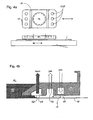
- FIG. 4a and 4b Another solution which has been proposed is to provide the liquid supply system with a seal member which extends along at least a part of a boundary of the space between the final element of the projection system and the substrate table.
- the seal member is substantially stationary relative to the projection system in the XY plane though there may be some relative movement in the Z direction (in the direction of the optical axis).
- a seal is formed between the seal member and the surface of the substrate.
- the seal is a contactless seal such as a gas seal.
- a gas seal is disclosed in European Patent Application No. 03252955.4 .
- the temperature control of the pressurized gas may be effected with reference to calibration measurements or with reference to readings from one or more temperature sensors 60.
- the output of the pressurized gas temperature controller 140 may be controlled so as to minimize a difference or differences between a target temperature or temperatures Tt and the temperature(s) provided by the temperature sensors 60, the convergence process being controlled by a feedback controller, such as a PID controller. That is to say, where a single temperature sensor 60 is present, the pressurized gas temperature controller 140 compares this one temperature reading with a single target temperature Tt.
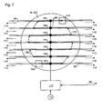
- An additional and/or alternative approach is to provide a dedicated seal member heater 220, which is arranged to provide a compensating heating power to those areas of the seal member 12 cooled by evaporation of the immersion liquid.
- the seal member heater 220 may be arranged to heat the substrate W directly. This may be achieved through the use of a radiation-emitting heater such as an infra-red heater, which has been described above in the context of possible substrate heaters 85/86.
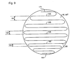
- the seal member heaters 220 are arranged around the vacuum exhaust inlet and may follow the geometry of the vacuum exhaust inlet in a plane perpendicular to the axis of the seal member 12 (into the page in the orientation depicted).
- the seal member temperature stabilizer 200 may control the output of the seal member heater 220 by reference to a calibration table 230 of required corrections, constructed from measurements of the seal member temperature as a function of one or more of the following: substrate temperature, pressurized gas flow rate, pressurized gas flow temperature, vacuum exhaust flow rate, vacuum exhaust temperature, pressurized gas relative humidity and immersion liquid temperature.
Applications Claiming Priority (1)
| Application Number | Priority Date | Filing Date | Title |
|---|---|---|---|
| US10/917,535 US7304715B2 (en) | 2004-08-13 | 2004-08-13 | Lithographic apparatus and device manufacturing method |
Publications (3)
| Publication Number | Publication Date |
|---|---|
| EP1628161A2 EP1628161A2 (en) | 2006-02-22 |
| EP1628161A3 EP1628161A3 (en) | 2006-06-07 |
| EP1628161B1 true EP1628161B1 (en) | 2012-11-28 |
Family
ID=34981965
Family Applications (1)
| Application Number | Title | Priority Date | Filing Date |
|---|---|---|---|
| EP05254783A Not-in-force EP1628161B1 (en) | 2004-08-13 | 2005-07-29 | Lithographic apparatus and device manufacturing method |
Country Status (7)
| Country | Link |
|---|---|
| US (7) | US7304715B2 (ja) |
| EP (1) | EP1628161B1 (ja) |
| JP (4) | JP4852278B2 (ja) |
| KR (1) | KR100760317B1 (ja) |
| CN (2) | CN1746775B (ja) |
| SG (2) | SG131107A1 (ja) |
| TW (1) | TWI322929B (ja) |
Families Citing this family (115)
| Publication number | Priority date | Publication date | Assignee | Title |
|---|---|---|---|---|
| US7372541B2 (en) * | 2002-11-12 | 2008-05-13 | Asml Netherlands B.V. | Lithographic apparatus and device manufacturing method |
| TWI232357B (en) | 2002-11-12 | 2005-05-11 | Asml Netherlands Bv | Lithographic apparatus and device manufacturing method |
| AU2003289236A1 (en) * | 2002-12-10 | 2004-06-30 | Nikon Corporation | Exposure apparatus and method for manufacturing device |
| CN106444292A (zh) | 2003-04-11 | 2017-02-22 | 株式会社尼康 | 沉浸式光刻装置、清洗方法、器件制造方法及液体沉浸式光刻装置 |
| TW201806001A (zh) | 2003-05-23 | 2018-02-16 | 尼康股份有限公司 | 曝光裝置及元件製造方法 |
| KR101728664B1 (ko) * | 2003-05-28 | 2017-05-02 | 가부시키가이샤 니콘 | 노광 방법, 노광 장치, 및 디바이스 제조 방법 |
| US7738074B2 (en) * | 2003-07-16 | 2010-06-15 | Asml Netherlands B.V. | Lithographic apparatus and device manufacturing method |
| JP4843503B2 (ja) * | 2004-01-20 | 2011-12-21 | カール・ツァイス・エスエムティー・ゲーエムベーハー | マイクロリソグラフィ投影露光装置および投影レンズのための測定装置 |
| KR101579361B1 (ko) * | 2004-02-04 | 2015-12-21 | 가부시키가이샤 니콘 | 노광 장치, 노광 방법 및 디바이스 제조 방법 |
| KR101440746B1 (ko) | 2004-06-09 | 2014-09-17 | 가부시키가이샤 니콘 | 노광 장치 및 디바이스 제조 방법 |
| US7304715B2 (en) | 2004-08-13 | 2007-12-04 | Asml Netherlands B.V. | Lithographic apparatus and device manufacturing method |
| JP2006134974A (ja) * | 2004-11-04 | 2006-05-25 | Canon Inc | 露光装置、判定方法及びデバイス製造方法 |
| SG124351A1 (en) * | 2005-01-14 | 2006-08-30 | Asml Netherlands Bv | Lithographic apparatus and device manufacturing method |
| JP4262252B2 (ja) * | 2005-03-02 | 2009-05-13 | キヤノン株式会社 | 露光装置 |
| JP5040646B2 (ja) * | 2005-03-23 | 2012-10-03 | 株式会社ニコン | 露光装置及び露光方法、並びにデバイス製造方法 |
| KR101555707B1 (ko) | 2005-04-18 | 2015-09-25 | 가부시키가이샤 니콘 | 노광 장치 및 노광 방법, 그리고 디바이스 제조 방법 |
| US7652746B2 (en) * | 2005-06-21 | 2010-01-26 | Asml Netherlands B.V. | Lithographic apparatus and device manufacturing method |
| US7751027B2 (en) | 2005-06-21 | 2010-07-06 | Asml Netherlands B.V. | Lithographic apparatus and device manufacturing method |
| US7417707B2 (en) * | 2005-06-29 | 2008-08-26 | Corbett Blaise L | Introduction of an intermediary refractive layer for immersion lithography |
| TWI345685B (en) * | 2005-09-06 | 2011-07-21 | Asml Netherlands Bv | Lithographic method |
| US7426011B2 (en) | 2005-09-12 | 2008-09-16 | Asml Netherlands B.V. | Method of calibrating a lithographic apparatus and device manufacturing method |
| JP4756984B2 (ja) * | 2005-10-07 | 2011-08-24 | キヤノン株式会社 | 露光装置、露光装置の制御方法およびデバイスの製造方法 |
| JP4125315B2 (ja) * | 2005-10-11 | 2008-07-30 | キヤノン株式会社 | 露光装置及びデバイス製造方法 |
| US7420188B2 (en) * | 2005-10-14 | 2008-09-02 | Taiwan Semiconductor Manufacturing Company, Ltd. | Exposure method and apparatus for immersion lithography |
| US7986395B2 (en) * | 2005-10-24 | 2011-07-26 | Taiwan Semiconductor Manufacturing Company, Ltd. | Immersion lithography apparatus and methods |
| TW200725195A (en) | 2005-12-06 | 2007-07-01 | Nikon Corp | Exposure method, exposure apparatus, and unit manufacturing method |
| US7420194B2 (en) * | 2005-12-27 | 2008-09-02 | Asml Netherlands B.V. | Lithographic apparatus and substrate edge seal |
| US7649611B2 (en) * | 2005-12-30 | 2010-01-19 | Asml Netherlands B.V. | Lithographic apparatus and device manufacturing method |
| JPWO2007080779A1 (ja) * | 2006-01-12 | 2009-06-11 | 株式会社ニコン | 物体搬送装置、露光装置、物体温調装置、物体搬送方法、及びマイクロデバイスの製造方法 |
| US8045134B2 (en) | 2006-03-13 | 2011-10-25 | Asml Netherlands B.V. | Lithographic apparatus, control system and device manufacturing method |
| US9477158B2 (en) | 2006-04-14 | 2016-10-25 | Asml Netherlands B.V. | Lithographic apparatus and device manufacturing method |
| US7675604B2 (en) * | 2006-05-04 | 2010-03-09 | Taiwan Semiconductor Manufacturing Company, Ltd. | Hood for immersion lithography |
| DE102006021797A1 (de) * | 2006-05-09 | 2007-11-15 | Carl Zeiss Smt Ag | Optische Abbildungseinrichtung mit thermischer Dämpfung |
| US7877895B2 (en) * | 2006-06-26 | 2011-02-01 | Tokyo Electron Limited | Substrate processing apparatus |
| US8564759B2 (en) * | 2006-06-29 | 2013-10-22 | Taiwan Semiconductor Manufacturing Company, Ltd. | Apparatus and method for immersion lithography |
| US7804582B2 (en) | 2006-07-28 | 2010-09-28 | Asml Netherlands B.V. | Lithographic apparatus, method of calibrating a lithographic apparatus and device manufacturing method |
| US8208116B2 (en) * | 2006-11-03 | 2012-06-26 | Taiwan Semiconductor Manufacturing Company, Ltd. | Immersion lithography system using a sealed wafer bath |
| US8253922B2 (en) | 2006-11-03 | 2012-08-28 | Taiwan Semiconductor Manufacturing Company, Ltd. | Immersion lithography system using a sealed wafer bath |
| US7932019B2 (en) * | 2006-11-13 | 2011-04-26 | Samsung Electronics Co., Ltd. | Gettering members, methods of forming the same, and methods of performing immersion lithography using the same |
| US8068208B2 (en) * | 2006-12-01 | 2011-11-29 | Taiwan Semiconductor Manufacturing Company, Ltd. | System and method for improving immersion scanner overlay performance |
| US20080137055A1 (en) * | 2006-12-08 | 2008-06-12 | Asml Netherlands B.V. | Lithographic apparatus and device manufacturing method |
| US7791709B2 (en) * | 2006-12-08 | 2010-09-07 | Asml Netherlands B.V. | Substrate support and lithographic process |
| US8416383B2 (en) * | 2006-12-13 | 2013-04-09 | Asml Netherlands B.V. | Lithographic apparatus and method |
| US7866637B2 (en) * | 2007-01-26 | 2011-01-11 | Asml Netherlands B.V. | Humidifying apparatus, lithographic apparatus and humidifying method |
| US8947629B2 (en) * | 2007-05-04 | 2015-02-03 | Asml Netherlands B.V. | Cleaning device, a lithographic apparatus and a lithographic apparatus cleaning method |
| US8011377B2 (en) * | 2007-05-04 | 2011-09-06 | Asml Netherlands B.V. | Cleaning device and a lithographic apparatus cleaning method |
| US7900641B2 (en) | 2007-05-04 | 2011-03-08 | Asml Netherlands B.V. | Cleaning device and a lithographic apparatus cleaning method |
| US7866330B2 (en) * | 2007-05-04 | 2011-01-11 | Asml Netherlands B.V. | Cleaning device, a lithographic apparatus and a lithographic apparatus cleaning method |
| US8264662B2 (en) | 2007-06-18 | 2012-09-11 | Taiwan Semiconductor Manufacturing Company, Ltd. | In-line particle detection for immersion lithography |
| TWI450047B (zh) | 2007-07-13 | 2014-08-21 | Mapper Lithography Ip Bv | 微影系統、夾緊方法及晶圓台 |
| US8705010B2 (en) * | 2007-07-13 | 2014-04-22 | Mapper Lithography Ip B.V. | Lithography system, method of clamping and wafer table |
| US9025126B2 (en) * | 2007-07-31 | 2015-05-05 | Nikon Corporation | Exposure apparatus adjusting method, exposure apparatus, and device fabricating method |
| US8582079B2 (en) * | 2007-08-14 | 2013-11-12 | Applied Materials, Inc. | Using phase difference of interference lithography for resolution enhancement |
| NL1036009A1 (nl) * | 2007-10-05 | 2009-04-07 | Asml Netherlands Bv | An Immersion Lithography Apparatus. |
| JP5369443B2 (ja) | 2008-02-05 | 2013-12-18 | 株式会社ニコン | ステージ装置、露光装置、露光方法、及びデバイス製造方法 |
| NL1036835A1 (nl) * | 2008-05-08 | 2009-11-11 | Asml Netherlands Bv | Lithographic Apparatus and Method. |
| NL2002964A1 (nl) * | 2008-06-16 | 2009-12-17 | Asml Netherlands Bv | Lithographic Apparatus, a Metrology Apparatus and a Method of Using the Apparatus. |
| EP2136250A1 (en) * | 2008-06-18 | 2009-12-23 | ASML Netherlands B.V. | Lithographic apparatus and method |
| EP2172766A1 (en) * | 2008-10-03 | 2010-04-07 | ASML Netherlands B.V. | Lithographic apparatus and humidity measurement system |
| NL2003758A (en) * | 2008-12-04 | 2010-06-07 | Asml Netherlands Bv | A member with a cleaning surface and a method of removing contamination. |
| US8739383B2 (en) * | 2009-04-20 | 2014-06-03 | Nikon Corporation | Method and apparatus for aligning mirror blocks of a multi-element mirror assembly |
| NL2004547A (en) * | 2009-05-14 | 2010-11-18 | Asml Netherlands Bv | An immersion lithographic apparatus and a device manufacturing method. |
| NL2004808A (en) | 2009-06-30 | 2011-01-12 | Asml Netherlands Bv | Fluid handling structure, lithographic apparatus and device manufacturing method. |
| NL2004980A (en) * | 2009-07-13 | 2011-01-17 | Asml Netherlands Bv | Heat transfers assembly, lithographic apparatus and manufacturing method. |
| NL2005009A (en) * | 2009-07-27 | 2011-01-31 | Asml Netherlands Bv | Lithographic apparatus and device manufacturing method. |
| NL2005207A (en) * | 2009-09-28 | 2011-03-29 | Asml Netherlands Bv | Heat pipe, lithographic apparatus and device manufacturing method. |
| JP5269128B2 (ja) * | 2010-03-12 | 2013-08-21 | エーエスエムエル ネザーランズ ビー.ブイ. | リソグラフィ装置および方法 |
| EP2381310B1 (en) | 2010-04-22 | 2015-05-06 | ASML Netherlands BV | Fluid handling structure and lithographic apparatus |
| NL2006536A (en) * | 2010-05-13 | 2011-11-15 | Asml Netherlands Bv | A substrate table, a lithographic apparatus, a method of flattening an edge of a substrate and a device manufacturing method. |
| NL2006913A (en) | 2010-07-16 | 2012-01-17 | Asml Netherlands Bv | Lithographic apparatus and method. |
| KR102002269B1 (ko) | 2010-07-30 | 2019-07-19 | 칼 짜이스 에스엠티 게엠베하 | Euv 노광 장치 |
| NL2007768A (en) | 2010-12-14 | 2012-06-18 | Asml Netherlands Bv | Substrate holder, lithographic apparatus, device manufacturing method, and method of manufacturing a substrate holder. |
| NL2007834A (en) * | 2010-12-23 | 2012-06-27 | Asml Netherlands Bv | Lithographic apparatus and removable member. |
| EP2490073B1 (en) | 2011-02-18 | 2015-09-23 | ASML Netherlands BV | Substrate holder, lithographic apparatus, and method of manufacturing a substrate holder |
| NL2008630A (en) * | 2011-04-27 | 2012-10-30 | Asml Netherlands Bv | Substrate holder, lithographic apparatus, device manufacturing method, and method of manufacturing a substrate holder. |
| NL2009189A (en) | 2011-08-17 | 2013-02-19 | Asml Netherlands Bv | Support table for a lithographic apparatus, lithographic apparatus and device manufacturing method. |
| SG188036A1 (en) | 2011-08-18 | 2013-03-28 | Asml Netherlands Bv | Lithographic apparatus, support table for a lithographic apparatus and device manufacturing method |
| NL2009272A (en) * | 2011-08-31 | 2013-03-04 | Asml Netherlands Bv | A fluid handling structure, a lithographic apparatus and a device manufacturing method. |
| JP5686779B2 (ja) | 2011-10-14 | 2015-03-18 | キヤノン株式会社 | インプリント装置、それを用いた物品の製造方法 |
| US9778579B2 (en) | 2011-11-10 | 2017-10-03 | Nikon Corporation | System and method for controlling a temperature of a reaction assembly |
| WO2013072144A1 (en) * | 2011-11-17 | 2013-05-23 | Asml Netherlands B.V. | Lithographic apparatus and device manufacturing method |
| WO2013113569A1 (en) | 2012-02-03 | 2013-08-08 | Asml Netherlands B.V. | Substrate holder and method of manufacturing a substrate holder |
| US9429857B2 (en) * | 2012-04-23 | 2016-08-30 | Asml Netherlands B.V. | Electrostatic clamp, lithographic apparatus and method |
| JP6122252B2 (ja) | 2012-05-01 | 2017-04-26 | キヤノン株式会社 | 露光装置及びデバイスの製造方法 |
| NL2010762A (en) | 2012-05-29 | 2013-12-02 | Asml Netherlands Bv | An object holder, a lithographic apparatus and a device manufacturing method. |
| JP6041541B2 (ja) * | 2012-06-04 | 2016-12-07 | キヤノン株式会社 | 露光装置及びデバイス製造方法 |
| JP2014086701A (ja) * | 2012-10-26 | 2014-05-12 | Canon Inc | 保持装置、リソグラフィ装置及び物品の製造方法 |
| JP2016507763A (ja) * | 2012-12-17 | 2016-03-10 | エーエスエムエル ネザーランズ ビー.ブイ. | リソグラフィ装置のための基板サポート及びリソグラフィ装置 |
| KR102209735B1 (ko) * | 2013-02-07 | 2021-02-01 | 에이에스엠엘 네델란즈 비.브이. | 리소그래피 장치 |
| US10216095B2 (en) | 2013-08-30 | 2019-02-26 | Asml Netherlands B.V. | Immersion lithographic apparatus |
| US9541846B2 (en) | 2013-09-06 | 2017-01-10 | Taiwan Semiconductor Manufacturing Co., Ltd. | Homogeneous thermal equalization with active device |
| EP3049869B1 (en) | 2013-09-27 | 2017-11-08 | ASML Netherlands B.V. | Support table for a lithographic apparatus, lithographic apparatus and device manufacturing method |
| JP6336275B2 (ja) * | 2013-12-26 | 2018-06-06 | キヤノン株式会社 | インプリント装置、および物品の製造方法 |
| CN103757591B (zh) * | 2013-12-31 | 2016-03-30 | 深圳市华星光电技术有限公司 | 一种坩埚设备及其在液晶面板生产中的应用 |
| US9575415B2 (en) * | 2014-05-22 | 2017-02-21 | Taiwan Semiconductor Manufacturing Company, Ltd. | Wafer stage temperature control |
| CN106462082B (zh) * | 2014-06-10 | 2018-05-18 | Asml荷兰有限公司 | 光刻设备及制造光刻设备的方法 |
| JP6251825B2 (ja) | 2014-06-16 | 2017-12-20 | エーエスエムエル ネザーランズ ビー.ブイ. | リソグラフィ装置、及び基板を搬送する方法 |
| WO2015193053A1 (en) | 2014-06-19 | 2015-12-23 | Asml Netherlands B.V. | Lithographic apparatus, object positioning system and device manufacturing method |
| JP6525567B2 (ja) * | 2014-12-02 | 2019-06-05 | キヤノン株式会社 | インプリント装置及び物品の製造方法 |
| CN107771303B (zh) | 2015-04-21 | 2021-06-04 | Asml荷兰有限公司 | 光刻设备 |
| CN107168015B (zh) * | 2016-02-29 | 2019-01-04 | 上海微电子装备(集团)股份有限公司 | 一种浸液限制机构及温度补偿方法 |
| JP2017183397A (ja) * | 2016-03-29 | 2017-10-05 | 株式会社東芝 | パターン転写装置及びパターン転写方法 |
| US9933314B2 (en) | 2016-06-30 | 2018-04-03 | Varian Semiconductor Equipment Associates, Inc. | Semiconductor workpiece temperature measurement system |
| CN109416406B (zh) * | 2016-07-05 | 2023-06-20 | 深圳帧观德芯科技有限公司 | 具有不同热膨胀系数的接合材料 |
| NL2019362A (en) * | 2016-09-02 | 2018-03-06 | Asml Netherlands Bv | Lithographic Apparatus |
| KR102499301B1 (ko) * | 2016-11-15 | 2023-02-10 | 에이에스엠엘 네델란즈 비.브이. | 방사선 분석 시스템 |
| US10503085B2 (en) * | 2017-11-16 | 2019-12-10 | Taiwan Semiconductor Manufacturing Co., Ltd. | Lithography apparatus and method |
| KR102511272B1 (ko) * | 2018-02-23 | 2023-03-16 | 삼성전자주식회사 | 노광 장치 및 이를 이용하는 반도체 장치의 제조 방법 |
| KR101924174B1 (ko) * | 2018-04-04 | 2019-02-22 | (주)유티아이 | 근적외선 필터 및 그 필터의 제조방법 |
| JP7034825B2 (ja) * | 2018-05-16 | 2022-03-14 | 株式会社ニューフレアテクノロジー | 荷電粒子ビーム描画装置及び荷電粒子ビーム描画方法 |
| US10788762B2 (en) * | 2019-02-25 | 2020-09-29 | Applied Materials, Inc. | Dynamic cooling control for thermal stabilization for lithography system |
| WO2021155991A1 (en) * | 2020-02-06 | 2021-08-12 | Asml Netherlands B.V. | Method of using a dual stage lithographic apparatus and lithographic apparatus |
| JP6842225B1 (ja) * | 2020-11-12 | 2021-03-17 | ハイソル株式会社 | チャックユニット及びチャックユニットの温度制御方法 |
| CN114264889B (zh) * | 2021-12-16 | 2023-07-21 | 中国工程物理研究院应用电子学研究所 | 一种高功率毫米波功率测量校准装置 |
| DE102021214981A1 (de) * | 2021-12-23 | 2023-06-29 | Carl Zeiss Smt Gmbh | Verfahren und trockenvorrichtung |
Family Cites Families (175)
| Publication number | Priority date | Publication date | Assignee | Title |
|---|---|---|---|---|
| DE242880C (ja) | ||||
| DE206607C (ja) | ||||
| DE224448C (ja) | ||||
| DE221563C (ja) | ||||
| GB1242527A (en) * | 1967-10-20 | 1971-08-11 | Kodak Ltd | Optical instruments |
| US3573975A (en) * | 1968-07-10 | 1971-04-06 | Ibm | Photochemical fabrication process |
| US4213698A (en) * | 1978-12-01 | 1980-07-22 | Bell Telephone Laboratories, Incorporated | Apparatus and method for holding and planarizing thin workpieces |
| DE2963537D1 (en) | 1979-07-27 | 1982-10-07 | Tabarelli Werner W | Optical lithographic method and apparatus for copying a pattern onto a semiconductor wafer |
| FR2474708B1 (fr) | 1980-01-24 | 1987-02-20 | Dme | Procede de microphotolithographie a haute resolution de traits |
| JPS5754317A (en) * | 1980-09-19 | 1982-03-31 | Hitachi Ltd | Method and device for forming pattern |
| US4509852A (en) * | 1980-10-06 | 1985-04-09 | Werner Tabarelli | Apparatus for the photolithographic manufacture of integrated circuit elements |
| US4346164A (en) * | 1980-10-06 | 1982-08-24 | Werner Tabarelli | Photolithographic method for the manufacture of integrated circuits |
| US4390273A (en) * | 1981-02-17 | 1983-06-28 | Censor Patent-Und Versuchsanstalt | Projection mask as well as a method and apparatus for the embedding thereof and projection printing system |
| JPS57153433A (en) * | 1981-03-18 | 1982-09-22 | Hitachi Ltd | Manufacturing device for semiconductor |
| JPS57169244A (en) * | 1981-04-13 | 1982-10-18 | Canon Inc | Temperature controller for mask and wafer |
| DD160756A3 (de) * | 1981-04-24 | 1984-02-29 | Gudrun Dietz | Anordnung zur verbesserung fotochemischer umsetzungsprozesse in fotoresistschichten |
| JPS58202448A (ja) | 1982-05-21 | 1983-11-25 | Hitachi Ltd | 露光装置 |
| DD206607A1 (de) | 1982-06-16 | 1984-02-01 | Mikroelektronik Zt Forsch Tech | Verfahren und vorrichtung zur beseitigung von interferenzeffekten |
| DD242880A1 (de) | 1983-01-31 | 1987-02-11 | Kuch Karl Heinz | Einrichtung zur fotolithografischen strukturuebertragung |
| JPS59144127A (ja) | 1983-02-07 | 1984-08-18 | Canon Inc | 像調整された光学装置 |
| JPS6018680U (ja) | 1983-07-13 | 1985-02-08 | 愛知電機株式会社 | 無整流子電動機 |
| US4564284A (en) * | 1983-09-12 | 1986-01-14 | Canon Kabushiki Kaisha | Semiconductor exposure apparatus |
| DD221563A1 (de) | 1983-09-14 | 1985-04-24 | Mikroelektronik Zt Forsch Tech | Immersionsobjektiv fuer die schrittweise projektionsabbildung einer maskenstruktur |
| JPS60163046A (ja) | 1984-02-03 | 1985-08-24 | Nippon Kogaku Kk <Nikon> | 投影露光光学装置及び投影露光方法 |
| DD224448A1 (de) | 1984-03-01 | 1985-07-03 | Zeiss Jena Veb Carl | Einrichtung zur fotolithografischen strukturuebertragung |
| JPS6265326A (ja) | 1985-09-18 | 1987-03-24 | Hitachi Ltd | 露光装置 |
| JPS6265326U (ja) | 1985-10-16 | 1987-04-23 | ||
| JPS62121417A (ja) | 1985-11-22 | 1987-06-02 | Hitachi Ltd | 液浸対物レンズ装置 |
| JPS62121417U (ja) | 1986-01-24 | 1987-08-01 | ||
| JPS63157419A (ja) | 1986-12-22 | 1988-06-30 | Toshiba Corp | 微細パタ−ン転写装置 |
| JPH033222Y2 (ja) | 1986-12-23 | 1991-01-28 | ||
| JPH07106317B2 (ja) | 1987-02-13 | 1995-11-15 | 触媒化成工業株式会社 | 炭化水素油の接触分解用触媒組成物の製造方法 |
| US4825247A (en) * | 1987-02-16 | 1989-04-25 | Canon Kabushiki Kaisha | Projection exposure apparatus |
| JPS63157419U (ja) | 1987-03-31 | 1988-10-14 | ||
| JPH01152639A (ja) | 1987-12-10 | 1989-06-15 | Canon Inc | 吸着保持装置 |
| US5040020A (en) * | 1988-03-31 | 1991-08-13 | Cornell Research Foundation, Inc. | Self-aligned, high resolution resonant dielectric lithography |
| FR2631165B1 (fr) * | 1988-05-05 | 1992-02-21 | Moulene Daniel | Support conditionneur de temperature pour petits objets tels que des composants semi-conducteurs et procede de regulation thermique utilisant ce support |
| JP2774574B2 (ja) * | 1989-05-30 | 1998-07-09 | キヤノン株式会社 | 露光装置 |
| EP0357423B1 (en) * | 1988-09-02 | 1995-03-15 | Canon Kabushiki Kaisha | An exposure apparatus |
| DE68922061T2 (de) * | 1988-10-03 | 1995-08-31 | Canon Kk | Vorrichtung zum Regeln der Temperatur. |
| US5231291A (en) * | 1989-08-01 | 1993-07-27 | Canon Kabushiki Kaisha | Wafer table and exposure apparatus with the same |
| JPH03209479A (ja) | 1989-09-06 | 1991-09-12 | Sanee Giken Kk | 露光方法 |
| JPH03198320A (ja) | 1989-12-27 | 1991-08-29 | Nikon Corp | 投影光学装置 |
| JPH0428216A (ja) | 1990-05-23 | 1992-01-30 | Matsushita Electric Ind Co Ltd | 露光装置 |
| NL9002077A (nl) | 1990-09-22 | 1992-04-16 | Imec Inter Uni Micro Electr | Sensor. |
| US5142132A (en) * | 1990-11-05 | 1992-08-25 | Litel Instruments | Adaptive optic wafer stepper illumination system |
| US5121256A (en) * | 1991-03-14 | 1992-06-09 | The Board Of Trustees Of The Leland Stanford Junior University | Lithography system employing a solid immersion lens |
| JPH04305917A (ja) | 1991-04-02 | 1992-10-28 | Nikon Corp | 密着型露光装置 |
| JPH04305915A (ja) | 1991-04-02 | 1992-10-28 | Nikon Corp | 密着型露光装置 |
| JP3210029B2 (ja) | 1991-06-11 | 2001-09-17 | キヤノン株式会社 | 画像処理装置及びその方法 |
| JP3218478B2 (ja) | 1992-09-04 | 2001-10-15 | 株式会社ニコン | 投影露光装置及び方法 |
| US5294778A (en) * | 1991-09-11 | 1994-03-15 | Lam Research Corporation | CVD platen heater system utilizing concentric electric heating elements |
| US5402224A (en) * | 1992-09-25 | 1995-03-28 | Nikon Corporation | Distortion inspecting method for projection optical system |
| JPH06124873A (ja) | 1992-10-09 | 1994-05-06 | Canon Inc | 液浸式投影露光装置 |
| JP2753930B2 (ja) | 1992-11-27 | 1998-05-20 | キヤノン株式会社 | 液浸式投影露光装置 |
| JP2520833B2 (ja) | 1992-12-21 | 1996-07-31 | 東京エレクトロン株式会社 | 浸漬式の液処理装置 |
| US6753948B2 (en) | 1993-04-27 | 2004-06-22 | Nikon Corporation | Scanning exposure method and apparatus |
| JPH0684757U (ja) | 1993-05-06 | 1994-12-02 | 太陽誘電株式会社 | 電源切替回路 |
| JPH07106317A (ja) | 1993-10-08 | 1995-04-21 | Sony Corp | 試料台 |
| JPH07220990A (ja) | 1994-01-28 | 1995-08-18 | Hitachi Ltd | パターン形成方法及びその露光装置 |
| US5612683A (en) * | 1994-08-26 | 1997-03-18 | Trempala; Dohn J. | Security key holder |
| JPH08124873A (ja) | 1994-10-24 | 1996-05-17 | Sony Corp | コンタクトホールの形成方法 |
| US5638687A (en) | 1994-11-21 | 1997-06-17 | Dainippon Screen Mfg. Co., Ltd. | Substrate cooling method and apparatus |
| JPH08316124A (ja) * | 1995-05-19 | 1996-11-29 | Hitachi Ltd | 投影露光方法及び露光装置 |
| JPH09270384A (ja) * | 1996-03-29 | 1997-10-14 | Nikon Corp | 温度制御装置及び露光装置 |
| WO1998009278A1 (en) * | 1996-08-26 | 1998-03-05 | Digital Papyrus Technologies | Method and apparatus for coupling an optical lens to a disk through a coupling medium having a relatively high index of refraction |
| US5825043A (en) * | 1996-10-07 | 1998-10-20 | Nikon Precision Inc. | Focusing and tilting adjustment system for lithography aligner, manufacturing apparatus or inspection apparatus |
| JPH10189242A (ja) | 1996-12-20 | 1998-07-21 | Sanyo Electric Co Ltd | 波長変換型発光装置 |
| JP3612920B2 (ja) | 1997-02-14 | 2005-01-26 | ソニー株式会社 | 光学記録媒体の原盤作製用露光装置 |
| TW404063B (en) * | 1997-02-27 | 2000-09-01 | Toshiba Corp | Semiconductor integrated circuit apparatus and semiconductor memory apparatus |
| JPH10255319A (ja) | 1997-03-12 | 1998-09-25 | Hitachi Maxell Ltd | 原盤露光装置及び方法 |
| JP3849822B2 (ja) | 1997-04-07 | 2006-11-22 | 株式会社ニコン | リソク゛ラフィシステム |
| US6882403B1 (en) * | 1997-04-07 | 2005-04-19 | Nikon Corporation | Lithography system and method |
| JP3747566B2 (ja) | 1997-04-23 | 2006-02-22 | 株式会社ニコン | 液浸型露光装置 |
| JP3817836B2 (ja) | 1997-06-10 | 2006-09-06 | 株式会社ニコン | 露光装置及びその製造方法並びに露光方法及びデバイス製造方法 |
| US5900354A (en) * | 1997-07-03 | 1999-05-04 | Batchelder; John Samuel | Method for optical inspection and lithography |
| JPH11195602A (ja) | 1997-10-07 | 1999-07-21 | Nikon Corp | 投影露光方法及び装置 |
| KR19990034784A (ko) | 1997-10-30 | 1999-05-15 | 윤종용 | 노광장비의 척부 |
| JPH11176727A (ja) | 1997-12-11 | 1999-07-02 | Nikon Corp | 投影露光装置 |
| AU1505699A (en) | 1997-12-12 | 1999-07-05 | Nikon Corporation | Projection exposure method and projection aligner |
| WO1999049504A1 (fr) | 1998-03-26 | 1999-09-30 | Nikon Corporation | Procede et systeme d'exposition par projection |
| JP3745167B2 (ja) * | 1998-07-29 | 2006-02-15 | キヤノン株式会社 | ステージ装置、露光装置およびデバイス製造方法ならびにステージ駆動方法 |
| JP2000058436A (ja) | 1998-08-11 | 2000-02-25 | Nikon Corp | 投影露光装置及び露光方法 |
| US6623639B2 (en) * | 1999-03-19 | 2003-09-23 | Bend Research, Inc. | Solvent-resistant microporous polybenzimidazole membranes |
| KR200224439Y1 (ko) | 1999-04-16 | 2001-05-15 | 나재흠 | 파일직기에 있어서 침포롤러 |
| TWI242111B (en) * | 1999-04-19 | 2005-10-21 | Asml Netherlands Bv | Gas bearings for use in vacuum chambers and their application in lithographic projection apparatus |
| US6225224B1 (en) | 1999-05-19 | 2001-05-01 | Infineon Technologies Norht America Corp. | System for dispensing polishing liquid during chemical mechanical polishing of a semiconductor wafer |
| AU5173100A (en) | 1999-05-27 | 2000-12-18 | Lam Research Corporation | Apparatus and methods for drying batches of wafers |
| US6322626B1 (en) * | 1999-06-08 | 2001-11-27 | Micron Technology, Inc. | Apparatus for controlling a temperature of a microelectronics substrate |
| JP4504479B2 (ja) | 1999-09-21 | 2010-07-14 | オリンパス株式会社 | 顕微鏡用液浸対物レンズ |
| JP2001118783A (ja) * | 1999-10-21 | 2001-04-27 | Nikon Corp | 露光方法及び装置、並びにデバイス製造方法 |
| JP2001272604A (ja) * | 2000-03-27 | 2001-10-05 | Olympus Optical Co Ltd | 液浸対物レンズおよびそれを用いた光学装置 |
| JP3870002B2 (ja) * | 2000-04-07 | 2007-01-17 | キヤノン株式会社 | 露光装置 |
| JP3531914B2 (ja) * | 2000-04-14 | 2004-05-31 | キヤノン株式会社 | 光学装置、露光装置及びデバイス製造方法 |
| JP3859937B2 (ja) * | 2000-06-02 | 2006-12-20 | 住友大阪セメント株式会社 | 静電チャック |
| US6699630B2 (en) * | 2000-07-07 | 2004-03-02 | Nikon Corporation | Method and apparatus for exposure, and device manufacturing method |
| TW591653B (en) * | 2000-08-08 | 2004-06-11 | Koninkl Philips Electronics Nv | Method of manufacturing an optically scannable information carrier |
| KR100866818B1 (ko) * | 2000-12-11 | 2008-11-04 | 가부시키가이샤 니콘 | 투영광학계 및 이 투영광학계를 구비한 노광장치 |
| JP4606600B2 (ja) * | 2001-01-09 | 2011-01-05 | 東京エレクトロン株式会社 | 処理空気供給装置及び方法 |
| US20020163629A1 (en) * | 2001-05-07 | 2002-11-07 | Michael Switkes | Methods and apparatus employing an index matching medium |
| US6954255B2 (en) | 2001-06-15 | 2005-10-11 | Canon Kabushiki Kaisha | Exposure apparatus |
| JP4302376B2 (ja) | 2001-09-03 | 2009-07-22 | 東京エレクトロン株式会社 | 液処理方法及び液処理装置 |
| US6600547B2 (en) * | 2001-09-24 | 2003-07-29 | Nikon Corporation | Sliding seal |
| US6696887B2 (en) | 2001-09-27 | 2004-02-24 | Matthew S. Taubman | Transistor-based interface circuitry |
| KR20050044371A (ko) * | 2001-11-07 | 2005-05-12 | 어플라이드 머티어리얼스, 인코포레이티드 | 광학 스폿 그리드 어레이 프린터 |
| JP4028216B2 (ja) | 2001-11-19 | 2007-12-26 | 大日本印刷株式会社 | 減容化可能なボトル |
| JP2003195476A (ja) * | 2001-12-27 | 2003-07-09 | Toshiba Corp | パターン形成装置およびパターン形成方法 |
| DE10229818A1 (de) * | 2002-06-28 | 2004-01-15 | Carl Zeiss Smt Ag | Verfahren zur Fokusdetektion und Abbildungssystem mit Fokusdetektionssystem |
| DE10210899A1 (de) | 2002-03-08 | 2003-09-18 | Zeiss Carl Smt Ag | Refraktives Projektionsobjektiv für Immersions-Lithographie |
| EP1532489A2 (en) | 2002-08-23 | 2005-05-25 | Nikon Corporation | Projection optical system and method for photolithography and exposure apparatus and method using same |
| JP3767815B2 (ja) * | 2002-08-26 | 2006-04-19 | 京楽産業株式会社 | メダル研磨装置 |
| US6788477B2 (en) * | 2002-10-22 | 2004-09-07 | Taiwan Semiconductor Manufacturing Co., Ltd. | Apparatus for method for immersion lithography |
| EP1420300B1 (en) | 2002-11-12 | 2015-07-29 | ASML Netherlands B.V. | Lithographic apparatus and device manufacturing method |
| CN101424881B (zh) | 2002-11-12 | 2011-11-30 | Asml荷兰有限公司 | 光刻投射装置 |
| KR100588124B1 (ko) | 2002-11-12 | 2006-06-09 | 에이에스엠엘 네델란즈 비.브이. | 리소그래피장치 및 디바이스제조방법 |
| EP1420298B1 (en) | 2002-11-12 | 2013-02-20 | ASML Netherlands B.V. | Lithographic apparatus |
| TWI232357B (en) * | 2002-11-12 | 2005-05-11 | Asml Netherlands Bv | Lithographic apparatus and device manufacturing method |
| SG121822A1 (en) * | 2002-11-12 | 2006-05-26 | Asml Netherlands Bv | Lithographic apparatus and device manufacturing method |
| DE60335595D1 (de) | 2002-11-12 | 2011-02-17 | Asml Netherlands Bv | Lithographischer Apparat mit Immersion und Verfahren zur Herstellung einer Vorrichtung |
| SG131766A1 (en) | 2002-11-18 | 2007-05-28 | Asml Netherlands Bv | Lithographic apparatus and device manufacturing method |
| TWI255971B (en) | 2002-11-29 | 2006-06-01 | Asml Netherlands Bv | Lithographic apparatus and device manufacturing method |
| DE10258718A1 (de) * | 2002-12-09 | 2004-06-24 | Carl Zeiss Smt Ag | Projektionsobjektiv, insbesondere für die Mikrolithographie, sowie Verfahren zur Abstimmung eines Projektionsobjektives |
| EP1429190B1 (en) * | 2002-12-10 | 2012-05-09 | Canon Kabushiki Kaisha | Exposure apparatus and method |
| KR20050085236A (ko) | 2002-12-10 | 2005-08-29 | 가부시키가이샤 니콘 | 노광 장치 및 디바이스 제조 방법 |
| AU2003289199A1 (en) | 2002-12-10 | 2004-06-30 | Nikon Corporation | Exposure apparatus and method for manufacturing device |
| EP1571700A4 (en) | 2002-12-10 | 2007-09-12 | Nikon Corp | OPTICAL DEVICE AND PROJECTION EXPOSURE DEVICE USING THE OPTICAL DEVICE |
| AU2003302831A1 (en) | 2002-12-10 | 2004-06-30 | Nikon Corporation | Exposure method, exposure apparatus and method for manufacturing device |
| KR101157002B1 (ko) | 2002-12-10 | 2012-06-21 | 가부시키가이샤 니콘 | 노광 장치 및 디바이스 제조 방법 |
| JP4232449B2 (ja) | 2002-12-10 | 2009-03-04 | 株式会社ニコン | 露光方法、露光装置、及びデバイス製造方法 |
| JP4352874B2 (ja) | 2002-12-10 | 2009-10-28 | 株式会社ニコン | 露光装置及びデバイス製造方法 |
| DE10257766A1 (de) | 2002-12-10 | 2004-07-15 | Carl Zeiss Smt Ag | Verfahren zur Einstellung einer gewünschten optischen Eigenschaft eines Projektionsobjektivs sowie mikrolithografische Projektionsbelichtungsanlage |
| KR101101737B1 (ko) | 2002-12-10 | 2012-01-05 | 가부시키가이샤 니콘 | 노광장치 및 노광방법, 디바이스 제조방법 |
| AU2003289236A1 (en) | 2002-12-10 | 2004-06-30 | Nikon Corporation | Exposure apparatus and method for manufacturing device |
| WO2004053957A1 (ja) | 2002-12-10 | 2004-06-24 | Nikon Corporation | 面位置検出装置、露光方法、及びデバイス製造方法 |
| CN100446179C (zh) | 2002-12-10 | 2008-12-24 | 株式会社尼康 | 曝光设备和器件制造法 |
| WO2004055803A1 (en) | 2002-12-13 | 2004-07-01 | Koninklijke Philips Electronics N.V. | Liquid removal in a method and device for irradiating spots on a layer |
| AU2003295177A1 (en) | 2002-12-19 | 2004-07-14 | Koninklijke Philips Electronics N.V. | Method and device for irradiating spots on a layer |
| CN100385535C (zh) | 2002-12-19 | 2008-04-30 | 皇家飞利浦电子股份有限公司 | 照射光敏层上斑点的方法和装置 |
| EP1431825A1 (en) * | 2002-12-20 | 2004-06-23 | ASML Netherlands B.V. | Lithographic apparatus, device manufacturing method, and substrate holder |
| US6781670B2 (en) * | 2002-12-30 | 2004-08-24 | Intel Corporation | Immersion lithography |
| KR20050110033A (ko) * | 2003-03-25 | 2005-11-22 | 가부시키가이샤 니콘 | 노광 장치 및 디바이스 제조 방법 |
| KR101176817B1 (ko) * | 2003-04-07 | 2012-08-24 | 가부시키가이샤 니콘 | 노광장치 및 디바이스 제조방법 |
| KR101178754B1 (ko) | 2003-04-10 | 2012-09-07 | 가부시키가이샤 니콘 | 액침 리소그래피 장치용 진공 배출을 포함하는 환경 시스템 |
| TWI295414B (en) * | 2003-05-13 | 2008-04-01 | Asml Netherlands Bv | Lithographic apparatus and device manufacturing method |
| KR101728664B1 (ko) | 2003-05-28 | 2017-05-02 | 가부시키가이샤 니콘 | 노광 방법, 노광 장치, 및 디바이스 제조 방법 |
| JP5143331B2 (ja) | 2003-05-28 | 2013-02-13 | 株式会社ニコン | 露光方法及び露光装置、並びにデバイス製造方法 |
| US6867844B2 (en) | 2003-06-19 | 2005-03-15 | Asml Holding N.V. | Immersion photolithography system and method using microchannel nozzles |
| US6809794B1 (en) | 2003-06-27 | 2004-10-26 | Asml Holding N.V. | Immersion photolithography system and method using inverted wafer-projection optics interface |
| US7738074B2 (en) | 2003-07-16 | 2010-06-15 | Asml Netherlands B.V. | Lithographic apparatus and device manufacturing method |
| US7326522B2 (en) | 2004-02-11 | 2008-02-05 | Asml Netherlands B.V. | Device manufacturing method and a substrate |
| US6954256B2 (en) | 2003-08-29 | 2005-10-11 | Asml Netherlands B.V. | Gradient immersion lithography |
| US7545481B2 (en) | 2003-11-24 | 2009-06-09 | Asml Netherlands B.V. | Lithographic apparatus and device manufacturing method |
| US7589818B2 (en) | 2003-12-23 | 2009-09-15 | Asml Netherlands B.V. | Lithographic apparatus, alignment apparatus, device manufacturing method, and a method of converting an apparatus |
| US7394521B2 (en) | 2003-12-23 | 2008-07-01 | Asml Netherlands B.V. | Lithographic apparatus and device manufacturing method |
| JP4429023B2 (ja) * | 2004-01-07 | 2010-03-10 | キヤノン株式会社 | 露光装置及びデバイス製造方法 |
| JP4843503B2 (ja) * | 2004-01-20 | 2011-12-21 | カール・ツァイス・エスエムティー・ゲーエムベーハー | マイクロリソグラフィ投影露光装置および投影レンズのための測定装置 |
| JP5167572B2 (ja) | 2004-02-04 | 2013-03-21 | 株式会社ニコン | 露光装置、露光方法及びデバイス製造方法 |
| KR101579361B1 (ko) | 2004-02-04 | 2015-12-21 | 가부시키가이샤 니콘 | 노광 장치, 노광 방법 및 디바이스 제조 방법 |
| US7050146B2 (en) | 2004-02-09 | 2006-05-23 | Asml Netherlands B.V. | Lithographic apparatus and device manufacturing method |
| JP4479269B2 (ja) * | 2004-02-20 | 2010-06-09 | 株式会社ニコン | 露光装置及びデバイス製造方法 |
| US7561251B2 (en) * | 2004-03-29 | 2009-07-14 | Asml Netherlands B.V. | Lithographic apparatus and device manufacturing method |
| JP4510494B2 (ja) * | 2004-03-29 | 2010-07-21 | キヤノン株式会社 | 露光装置 |
| US20050229854A1 (en) * | 2004-04-15 | 2005-10-20 | Tokyo Electron Limited | Method and apparatus for temperature change and control |
| JP2005310933A (ja) * | 2004-04-20 | 2005-11-04 | Nikon Corp | 基板保持部材、露光装置及びデバイス製造方法 |
| US7501226B2 (en) * | 2004-06-23 | 2009-03-10 | Taiwan Semiconductor Manufacturing Co., Ltd. | Immersion lithography system with wafer sealing mechanisms |
| US8769126B2 (en) * | 2004-06-24 | 2014-07-01 | International Business Machines Corporation | Expanded membership access control in a collaborative environment |
| JP2006013130A (ja) * | 2004-06-25 | 2006-01-12 | Nikon Corp | 露光装置、露光方法、及びデバイスの製造方法 |
| US20060001851A1 (en) * | 2004-07-01 | 2006-01-05 | Grant Robert B | Immersion photolithography system |
| US7304715B2 (en) * | 2004-08-13 | 2007-12-04 | Asml Netherlands B.V. | Lithographic apparatus and device manufacturing method |
| US7532310B2 (en) | 2004-10-22 | 2009-05-12 | Asml Netherlands B.V. | Apparatus, method for supporting and/or thermally conditioning a substrate, a support table, and a chuck |
| US20060228632A1 (en) * | 2005-04-11 | 2006-10-12 | Boyer James L | Treated filler and process for producing |
| US7652746B2 (en) * | 2005-06-21 | 2010-01-26 | Asml Netherlands B.V. | Lithographic apparatus and device manufacturing method |
| US20070007316A1 (en) * | 2005-07-08 | 2007-01-11 | John Witczak | Bicycle carrier |
| JP2010034605A (ja) | 2009-11-17 | 2010-02-12 | Canon Inc | 露光装置及びデバイス製造方法 |
| NL2007768A (en) * | 2010-12-14 | 2012-06-18 | Asml Netherlands Bv | Substrate holder, lithographic apparatus, device manufacturing method, and method of manufacturing a substrate holder. |
-
2004
- 2004-08-13 US US10/917,535 patent/US7304715B2/en active Active
-
2005
- 2005-07-29 EP EP05254783A patent/EP1628161B1/en not_active Not-in-force
- 2005-08-08 SG SG200701400-4A patent/SG131107A1/en unknown
- 2005-08-08 SG SG200505017A patent/SG120255A1/en unknown
- 2005-08-12 CN CN2005101132352A patent/CN1746775B/zh active Active
- 2005-08-12 TW TW094127593A patent/TWI322929B/zh active
- 2005-08-12 CN CN2010101865871A patent/CN101923290B/zh active Active
- 2005-08-12 JP JP2005233909A patent/JP4852278B2/ja active Active
- 2005-08-12 KR KR1020050074411A patent/KR100760317B1/ko active IP Right Grant
- 2005-08-17 US US11/205,325 patent/US7804575B2/en active Active
-
2009
- 2009-02-04 JP JP2009024156A patent/JP5275067B2/ja active Active
-
2010
- 2010-08-26 US US12/869,560 patent/US9268242B2/en not_active Expired - Fee Related
-
2011
- 2011-11-03 US US13/288,831 patent/US9188880B2/en active Active
- 2011-12-27 JP JP2011285516A patent/JP5699072B2/ja active Active
-
2013
- 2013-11-01 JP JP2013228111A patent/JP5699197B2/ja active Active
-
2015
- 2015-10-13 US US14/882,241 patent/US10254663B2/en active Active
-
2019
- 2019-04-05 US US16/376,535 patent/US10838310B2/en active Active
-
2020
- 2020-11-13 US US17/098,073 patent/US11378893B2/en active Active
Also Published As
Similar Documents
| Publication | Publication Date | Title |
|---|---|---|
| US11378893B2 (en) | Lithographic apparatus and device manufacturing method involving a heater | |
| US10656538B2 (en) | Lithographic apparatus and device manufacturing method | |
| US10761433B2 (en) | Lithographic apparatus and device manufacturing method | |
| US7751027B2 (en) | Lithographic apparatus and device manufacturing method | |
| US20100245791A1 (en) | Lithographic apparatus and device manufacturing method | |
| US8994917B2 (en) | Temperature stabilization system to stabilize a temperature of an article | |
| EP1498781B1 (en) | Immersion lithographic apparatus and device manufacturing method |
Legal Events
| Date | Code | Title | Description |
|---|---|---|---|
| PUAI | Public reference made under article 153(3) epc to a published international application that has entered the european phase |
Free format text: ORIGINAL CODE: 0009012 |
|
| AK | Designated contracting states |
Kind code of ref document: A2 Designated state(s): AT BE BG CH CY CZ DE DK EE ES FI FR GB GR HU IE IS IT LI LT LU LV MC NL PL PT RO SE SI SK TR |
|
| AX | Request for extension of the european patent |
Extension state: AL BA HR MK YU |
|
| PUAL | Search report despatched |
Free format text: ORIGINAL CODE: 0009013 |
|
| AK | Designated contracting states |
Kind code of ref document: A3 Designated state(s): AT BE BG CH CY CZ DE DK EE ES FI FR GB GR HU IE IS IT LI LT LU LV MC NL PL PT RO SE SI SK TR |
|
| AX | Request for extension of the european patent |
Extension state: AL BA HR MK YU |
|
| 17P | Request for examination filed |
Effective date: 20061123 |
|
| AKX | Designation fees paid |
Designated state(s): DE FR GB IT NL |
|
| GRAP | Despatch of communication of intention to grant a patent |
Free format text: ORIGINAL CODE: EPIDOSNIGR1 |
|
| RIN1 | Information on inventor provided before grant (corrected) |
Inventor name: SCHOONDERMARK, BART LEONARD PETER Inventor name: SMEETS, MARTIN FRANS PIERRE Inventor name: GOORMAN, KOEN Inventor name: QUAEDACKERS, JOHANNES ANNA Inventor name: VAN DER NET, ANTONIUS JOHANNUS Inventor name: OTTENS, JOOST JEROEN Inventor name: REUHMAN-HUISKEN, MARIA ELISABETH Inventor name: TEN KATE, NICOLAAS Inventor name: JANSSEN, FRANCISCUS JOHANNES JOSEPH Inventor name: STAVENGA, MARCO KOERT Inventor name: RIEPEN, MICHEL Inventor name: MERTENS, JEROEN JOHANNES SOPHIA MARIA Inventor name: MUITJENS, MARCEL JOHANNUS ELISABETH HUBERTUS Inventor name: DE MOL, CHRISTIANUS GERARDUS MARIA Inventor name: LOOPSTRA, ERIK ROELOF Inventor name: VAN MEER, ASCHWIN LODEWIJK HENDRICUS JOHANNES Inventor name: TINNEMANS, PATRICIUS ALOYSIUS JACOBUS Inventor name: MENCHTCHIKOV, BORIS Inventor name: MOERMAN, RICHARD Inventor name: BOOM, HERMAN Inventor name: DE JONG, FREDERIK EDUARD Inventor name: VERHAGEN, MARTINUS CORNELIS MARIA Inventor name: VERSPAIJ, JACOBUS JOHANNUS LEONARDUS HENDRICUS Inventor name: NIHTIANOV, STOYAN Inventor name: JACOBS, JOHANNES HENRICUS WILHELMUS Inventor name: CADEE, THEODORUS PETRUS MARIA |
|
| GRAS | Grant fee paid |
Free format text: ORIGINAL CODE: EPIDOSNIGR3 |
|
| GRAA | (expected) grant |
Free format text: ORIGINAL CODE: 0009210 |
|
| AK | Designated contracting states |
Kind code of ref document: B1 Designated state(s): DE FR GB IT NL |
|
| REG | Reference to a national code |
Ref country code: GB Ref legal event code: FG4D |
|
| REG | Reference to a national code |
Ref country code: DE Ref legal event code: R096 Ref document number: 602005037164 Country of ref document: DE Effective date: 20130124 |
|
| REG | Reference to a national code |
Ref country code: NL Ref legal event code: VDEP Effective date: 20121128 |
|
| PG25 | Lapsed in a contracting state [announced via postgrant information from national office to epo] |
Ref country code: IT Free format text: LAPSE BECAUSE OF FAILURE TO SUBMIT A TRANSLATION OF THE DESCRIPTION OR TO PAY THE FEE WITHIN THE PRESCRIBED TIME-LIMIT Effective date: 20121128 Ref country code: NL Free format text: LAPSE BECAUSE OF FAILURE TO SUBMIT A TRANSLATION OF THE DESCRIPTION OR TO PAY THE FEE WITHIN THE PRESCRIBED TIME-LIMIT Effective date: 20121128 |
|
| PLBE | No opposition filed within time limit |
Free format text: ORIGINAL CODE: 0009261 |
|
| STAA | Information on the status of an ep patent application or granted ep patent |
Free format text: STATUS: NO OPPOSITION FILED WITHIN TIME LIMIT |
|
| 26N | No opposition filed |
Effective date: 20130829 |
|
| REG | Reference to a national code |
Ref country code: DE Ref legal event code: R097 Ref document number: 602005037164 Country of ref document: DE Effective date: 20130829 |
|
| GBPC | Gb: european patent ceased through non-payment of renewal fee |
Effective date: 20130729 |
|
| PG25 | Lapsed in a contracting state [announced via postgrant information from national office to epo] |
Ref country code: GB Free format text: LAPSE BECAUSE OF NON-PAYMENT OF DUE FEES Effective date: 20130729 |
|
| REG | Reference to a national code |
Ref country code: FR Ref legal event code: PLFP Year of fee payment: 12 |
|
| REG | Reference to a national code |
Ref country code: FR Ref legal event code: PLFP Year of fee payment: 13 |
|
| REG | Reference to a national code |
Ref country code: FR Ref legal event code: PLFP Year of fee payment: 14 |
|
| PGFP | Annual fee paid to national office [announced via postgrant information from national office to epo] |
Ref country code: FR Payment date: 20180725 Year of fee payment: 14 Ref country code: DE Payment date: 20180723 Year of fee payment: 14 |
|
| REG | Reference to a national code |
Ref country code: DE Ref legal event code: R119 Ref document number: 602005037164 Country of ref document: DE |
|
| PG25 | Lapsed in a contracting state [announced via postgrant information from national office to epo] |
Ref country code: DE Free format text: LAPSE BECAUSE OF NON-PAYMENT OF DUE FEES Effective date: 20200201 |
|
| PG25 | Lapsed in a contracting state [announced via postgrant information from national office to epo] |
Ref country code: FR Free format text: LAPSE BECAUSE OF NON-PAYMENT OF DUE FEES Effective date: 20190731 |