EP1547158B1 - Elektrode für fotovoltaische zellen, fotovoltaische zelle und fotovoltaisches modul - Google Patents
Elektrode für fotovoltaische zellen, fotovoltaische zelle und fotovoltaisches modul Download PDFInfo
- Publication number
- EP1547158B1 EP1547158B1 EP03790589A EP03790589A EP1547158B1 EP 1547158 B1 EP1547158 B1 EP 1547158B1 EP 03790589 A EP03790589 A EP 03790589A EP 03790589 A EP03790589 A EP 03790589A EP 1547158 B1 EP1547158 B1 EP 1547158B1
- Authority
- EP
- European Patent Office
- Prior art keywords
- wires
- electrode
- terminal
- bars
- frame
- Prior art date
- Legal status (The legal status is an assumption and is not a legal conclusion. Google has not performed a legal analysis and makes no representation as to the accuracy of the status listed.)
- Expired - Lifetime
Links
- 239000011248 coating agent Substances 0.000 claims abstract description 30
- 238000000576 coating method Methods 0.000 claims abstract description 30
- 239000000956 alloy Substances 0.000 claims abstract description 23
- 229910045601 alloy Inorganic materials 0.000 claims abstract description 22
- 239000012790 adhesive layer Substances 0.000 claims abstract description 18
- 238000002844 melting Methods 0.000 claims abstract description 10
- 230000008018 melting Effects 0.000 claims abstract description 10
- 230000003667 anti-reflective effect Effects 0.000 claims description 5
- 238000005476 soldering Methods 0.000 claims 1
- 229910000679 solder Inorganic materials 0.000 abstract description 2
- 239000010408 film Substances 0.000 description 44
- 235000012431 wafers Nutrition 0.000 description 37
- 239000000853 adhesive Substances 0.000 description 31
- 230000001070 adhesive effect Effects 0.000 description 31
- 239000000463 material Substances 0.000 description 20
- 238000004519 manufacturing process Methods 0.000 description 17
- 238000010438 heat treatment Methods 0.000 description 14
- 238000003825 pressing Methods 0.000 description 10
- 239000004065 semiconductor Substances 0.000 description 9
- 229910052751 metal Inorganic materials 0.000 description 8
- 239000002184 metal Substances 0.000 description 8
- 239000011521 glass Substances 0.000 description 5
- 238000010276 construction Methods 0.000 description 4
- 239000002245 particle Substances 0.000 description 3
- 238000013082 photovoltaic technology Methods 0.000 description 3
- 239000011241 protective layer Substances 0.000 description 3
- XUIMIQQOPSSXEZ-UHFFFAOYSA-N Silicon Chemical compound [Si] XUIMIQQOPSSXEZ-UHFFFAOYSA-N 0.000 description 2
- 229910052782 aluminium Inorganic materials 0.000 description 2
- XAGFODPZIPBFFR-UHFFFAOYSA-N aluminium Chemical compound [Al] XAGFODPZIPBFFR-UHFFFAOYSA-N 0.000 description 2
- 239000004020 conductor Substances 0.000 description 2
- 229920001577 copolymer Polymers 0.000 description 2
- 239000012799 electrically-conductive coating Substances 0.000 description 2
- 238000005516 engineering process Methods 0.000 description 2
- 229920002313 fluoropolymer Polymers 0.000 description 2
- 239000004811 fluoropolymer Substances 0.000 description 2
- 229920000642 polymer Polymers 0.000 description 2
- 229920002620 polyvinyl fluoride Polymers 0.000 description 2
- 230000005855 radiation Effects 0.000 description 2
- 229910052710 silicon Inorganic materials 0.000 description 2
- 239000010703 silicon Substances 0.000 description 2
- 239000010409 thin film Substances 0.000 description 2
- QTBSBXVTEAMEQO-UHFFFAOYSA-M Acetate Chemical compound CC([O-])=O QTBSBXVTEAMEQO-UHFFFAOYSA-M 0.000 description 1
- 229920002799 BoPET Polymers 0.000 description 1
- 229920000298 Cellophane Polymers 0.000 description 1
- RYGMFSIKBFXOCR-UHFFFAOYSA-N Copper Chemical compound [Cu] RYGMFSIKBFXOCR-UHFFFAOYSA-N 0.000 description 1
- 229920000297 Rayon Polymers 0.000 description 1
- 229920006355 Tefzel Polymers 0.000 description 1
- 239000003522 acrylic cement Substances 0.000 description 1
- 239000004411 aluminium Substances 0.000 description 1
- 229910021417 amorphous silicon Inorganic materials 0.000 description 1
- 239000006117 anti-reflective coating Substances 0.000 description 1
- 229910052797 bismuth Inorganic materials 0.000 description 1
- DQXBYHZEEUGOBF-UHFFFAOYSA-N but-3-enoic acid;ethene Chemical compound C=C.OC(=O)CC=C DQXBYHZEEUGOBF-UHFFFAOYSA-N 0.000 description 1
- 229910052793 cadmium Inorganic materials 0.000 description 1
- 238000001816 cooling Methods 0.000 description 1
- 239000011889 copper foil Substances 0.000 description 1
- 238000005538 encapsulation Methods 0.000 description 1
- 229920006332 epoxy adhesive Polymers 0.000 description 1
- 239000003822 epoxy resin Substances 0.000 description 1
- QHSJIZLJUFMIFP-UHFFFAOYSA-N ethene;1,1,2,2-tetrafluoroethene Chemical compound C=C.FC(F)=C(F)F QHSJIZLJUFMIFP-UHFFFAOYSA-N 0.000 description 1
- 229920000840 ethylene tetrafluoroethylene copolymer Polymers 0.000 description 1
- 239000005038 ethylene vinyl acetate Substances 0.000 description 1
- -1 fluororesin Polymers 0.000 description 1
- 239000011888 foil Substances 0.000 description 1
- 229910052733 gallium Inorganic materials 0.000 description 1
- 239000003292 glue Substances 0.000 description 1
- 229910052738 indium Inorganic materials 0.000 description 1
- AMGQUBHHOARCQH-UHFFFAOYSA-N indium;oxotin Chemical compound [In].[Sn]=O AMGQUBHHOARCQH-UHFFFAOYSA-N 0.000 description 1
- 238000003475 lamination Methods 0.000 description 1
- 239000010410 layer Substances 0.000 description 1
- 229910052745 lead Inorganic materials 0.000 description 1
- 150000002739 metals Chemical class 0.000 description 1
- 238000000034 method Methods 0.000 description 1
- 229910021421 monocrystalline silicon Inorganic materials 0.000 description 1
- 239000010813 municipal solid waste Substances 0.000 description 1
- 230000003287 optical effect Effects 0.000 description 1
- 229920001200 poly(ethylene-vinyl acetate) Polymers 0.000 description 1
- 229920003229 poly(methyl methacrylate) Polymers 0.000 description 1
- 229920002492 poly(sulfone) Polymers 0.000 description 1
- 229920006122 polyamide resin Polymers 0.000 description 1
- 229910021420 polycrystalline silicon Inorganic materials 0.000 description 1
- 229920000647 polyepoxide Polymers 0.000 description 1
- 239000004926 polymethyl methacrylate Substances 0.000 description 1
- 229920001289 polyvinyl ether Polymers 0.000 description 1
- 239000002964 rayon Substances 0.000 description 1
- 229920005989 resin Polymers 0.000 description 1
- 239000011347 resin Substances 0.000 description 1
- 238000007650 screen-printing Methods 0.000 description 1
- 229910052709 silver Inorganic materials 0.000 description 1
- 229910001220 stainless steel Inorganic materials 0.000 description 1
- 239000010935 stainless steel Substances 0.000 description 1
- 229910052718 tin Inorganic materials 0.000 description 1
- 229910052719 titanium Inorganic materials 0.000 description 1
Images


Classifications
-
- H—ELECTRICITY
- H01—ELECTRIC ELEMENTS
- H01L—SEMICONDUCTOR DEVICES NOT COVERED BY CLASS H10
- H01L31/00—Semiconductor devices sensitive to infrared radiation, light, electromagnetic radiation of shorter wavelength or corpuscular radiation and specially adapted either for the conversion of the energy of such radiation into electrical energy or for the control of electrical energy by such radiation; Processes or apparatus specially adapted for the manufacture or treatment thereof or of parts thereof; Details thereof
- H01L31/02—Details
- H01L31/0224—Electrodes
- H01L31/022408—Electrodes for devices characterised by at least one potential jump barrier or surface barrier
- H01L31/022425—Electrodes for devices characterised by at least one potential jump barrier or surface barrier for solar cells
-
- H—ELECTRICITY
- H01—ELECTRIC ELEMENTS
- H01L—SEMICONDUCTOR DEVICES NOT COVERED BY CLASS H10
- H01L31/00—Semiconductor devices sensitive to infrared radiation, light, electromagnetic radiation of shorter wavelength or corpuscular radiation and specially adapted either for the conversion of the energy of such radiation into electrical energy or for the control of electrical energy by such radiation; Processes or apparatus specially adapted for the manufacture or treatment thereof or of parts thereof; Details thereof
- H01L31/04—Semiconductor devices sensitive to infrared radiation, light, electromagnetic radiation of shorter wavelength or corpuscular radiation and specially adapted either for the conversion of the energy of such radiation into electrical energy or for the control of electrical energy by such radiation; Processes or apparatus specially adapted for the manufacture or treatment thereof or of parts thereof; Details thereof adapted as photovoltaic [PV] conversion devices
- H01L31/042—PV modules or arrays of single PV cells
- H01L31/05—Electrical interconnection means between PV cells inside the PV module, e.g. series connection of PV cells
- H01L31/0504—Electrical interconnection means between PV cells inside the PV module, e.g. series connection of PV cells specially adapted for series or parallel connection of solar cells in a module
- H01L31/0508—Electrical interconnection means between PV cells inside the PV module, e.g. series connection of PV cells specially adapted for series or parallel connection of solar cells in a module the interconnection means having a particular shape
-
- H—ELECTRICITY
- H01—ELECTRIC ELEMENTS
- H01L—SEMICONDUCTOR DEVICES NOT COVERED BY CLASS H10
- H01L31/00—Semiconductor devices sensitive to infrared radiation, light, electromagnetic radiation of shorter wavelength or corpuscular radiation and specially adapted either for the conversion of the energy of such radiation into electrical energy or for the control of electrical energy by such radiation; Processes or apparatus specially adapted for the manufacture or treatment thereof or of parts thereof; Details thereof
- H01L31/04—Semiconductor devices sensitive to infrared radiation, light, electromagnetic radiation of shorter wavelength or corpuscular radiation and specially adapted either for the conversion of the energy of such radiation into electrical energy or for the control of electrical energy by such radiation; Processes or apparatus specially adapted for the manufacture or treatment thereof or of parts thereof; Details thereof adapted as photovoltaic [PV] conversion devices
- H01L31/042—PV modules or arrays of single PV cells
- H01L31/05—Electrical interconnection means between PV cells inside the PV module, e.g. series connection of PV cells
- H01L31/0504—Electrical interconnection means between PV cells inside the PV module, e.g. series connection of PV cells specially adapted for series or parallel connection of solar cells in a module
- H01L31/0512—Electrical interconnection means between PV cells inside the PV module, e.g. series connection of PV cells specially adapted for series or parallel connection of solar cells in a module made of a particular material or composition of materials
-
- H—ELECTRICITY
- H01—ELECTRIC ELEMENTS
- H01L—SEMICONDUCTOR DEVICES NOT COVERED BY CLASS H10
- H01L2924/00—Indexing scheme for arrangements or methods for connecting or disconnecting semiconductor or solid-state bodies as covered by H01L24/00
- H01L2924/0001—Technical content checked by a classifier
- H01L2924/0002—Not covered by any one of groups H01L24/00, H01L24/00 and H01L2224/00
-
- H—ELECTRICITY
- H05—ELECTRIC TECHNIQUES NOT OTHERWISE PROVIDED FOR
- H05K—PRINTED CIRCUITS; CASINGS OR CONSTRUCTIONAL DETAILS OF ELECTRIC APPARATUS; MANUFACTURE OF ASSEMBLAGES OF ELECTRICAL COMPONENTS
- H05K3/00—Apparatus or processes for manufacturing printed circuits
- H05K3/10—Apparatus or processes for manufacturing printed circuits in which conductive material is applied to the insulating support in such a manner as to form the desired conductive pattern
-
- Y—GENERAL TAGGING OF NEW TECHNOLOGICAL DEVELOPMENTS; GENERAL TAGGING OF CROSS-SECTIONAL TECHNOLOGIES SPANNING OVER SEVERAL SECTIONS OF THE IPC; TECHNICAL SUBJECTS COVERED BY FORMER USPC CROSS-REFERENCE ART COLLECTIONS [XRACs] AND DIGESTS
- Y02—TECHNOLOGIES OR APPLICATIONS FOR MITIGATION OR ADAPTATION AGAINST CLIMATE CHANGE
- Y02E—REDUCTION OF GREENHOUSE GAS [GHG] EMISSIONS, RELATED TO ENERGY GENERATION, TRANSMISSION OR DISTRIBUTION
- Y02E10/00—Energy generation through renewable energy sources
- Y02E10/50—Photovoltaic [PV] energy
Definitions
- the invention relates to an electrode for contacting electrically conductive surfaces, in particular for contacting one or a plurality of photovoltaic (PV) elements being part of a photovoltaic cell or solar cell.
- the invention further relates to photovoltaic cells produced with this electrode.
- PV cells comprise a semiconductor element with a junction of the type (n + n(or p)p + ) on the basis of mono- or multicrystalline silicon, amorphous silicon and other thin-film semiconductors with an embedded p-n junction.
- One surface of the element is usually covered with a metal layer, such as aluminum or stainless steel, while the other surface is provided with an anti-reflective coating. Both surfaces are in contact with electrodes, which collect and carry off the generated electrical energy.
- This structure is embedded between transparent protective layers, such as glass.
- the electrodes are all produced using screen-printing technology. However, electrodes produced this way have a high series resistance. Apart from this, expensive devices and equipment are required for the production and cost reduction is limited when this technology is employed.
- US 4 380 112 A discloses a photovoltaic element comprising an electrode for contacting a surface of said PV element, said electrode comprising an electrically insulating optically transparent carrier.
- the wires of the electrode are embedded in the electrically insulating optically transparent carrier so that the electrode wires are exposed at one, the "inner" side thereof.
- Completion of the PV element is effected by electrostatically bonding the inner surface of the transparent film, together with the mesh components, to the exposed face of the front semiconductor element.
- the electrically insulating, optically transparent film is made from glass so that embedding the wire mesh into the film involves pressing and heating the structure to a temperature of about 700 °C (glass melting point).
- a permanent contact between the metallic wires and the semiconductor surface is formed by an electrostatically bonding step, i. e. a strong voltage is applied across the glass + metallic wire + semiconductor sandwich that is again heated up to 700°C.
- EP 0 807 980 A (Canon KK ) and US 5 759 291 A (Ichinose et al. ) disclose a semiconductor element (wafer) with parallel metallic contact or current collecting wires (electrodes) which are fixed to the surface of the element by means of a conductive adhesive in which conductive particles are dispersed.
- the electrode wires are arranged in parallel between connecting conductors which are running along the edges of the element.
- the ohmic contact resistance between the semiconductor surface and the wires is relatively high , which results in a high energy loss and a low efficiency, especially under concentrated solar radiation. Also, the production of such PV cell is rather complicated.
- US 5 457 057 A describes a current collecting electrode comprising metal wires, at least a part of said metal wires being coated by conductive paste.
- an object of the present invention to provide for an electrode, in particular for PV elements, which can be produced effectively as a separate product and attached to the surface to be contacted in an effective and gentle manner.
- a further objective of the invention is to provide for a PV cell which allows, by using such an electrode, lowering the combined series resistance and the production costs of PV cells and PV modules and enhancement of their efficiency.
- an adhesive layer is provided on one surface of the electrically insulating, optically transparent film, the electrically conductive wires being embedded into said adhesive layer, a part of the surfaces of said wires protruding from the adhesive layer, and wherein at least on the surface protruding from the adhesive layer said wires are covered by a coating consisting of an alloy with a low melting point.
- the adhesive layer must be heated only to a very low temperature (melting point of the adhesive layer of about 100 °C): A permanent contact between the metallic wire and the semiconductor surface is formed after pressure is applied on the polymeric film with the preliminarily embedded metallic wire that is pressed and heated only up to 130 °C. Thereby an intimate mechanical and electrical contact is obtained between the surface to be contacted and the wire.
- a second plurality of wires substantially running parallel to each other is disposed between the transparent film and the wires of said first plurality, the wires of the first and second pluralities forming together a mesh, and the wires of the second plurality being electrically connected to a second terminal bar.
- first and second terminal bars are electrically connected to each other.
- the terminal bar(s) may be provided at the respective ends of the wires.
- terminal bar(s) are preferably provided at opposite ends of the wires of the first or of the first and second pluralities of wires outside the contour of the photovoltaic element, to the surface of which the wires are to be connected.
- the first and second terminal bars are preferably connected to form an angle.
- terminal bars are formed as a U-shaped frame, the wires of one of the two pluralities being connected to the base and the wires of the other plurality being connected to the free legs of the U.
- the terminal bars are preferably extending over the length of two adjacent photovoltaic elements to be connected and that a step is provided in their centre, so that a plurality of terminal bars can be fit together forming one row, in which the one half of a terminal bar is arranged below or above the lower or upper halves, respectively, of the neighbouring terminal bar, wherein between the terminal bars an insulating film is provided.
- terminal bars may be formed as a closed frame, the open area (window) of said frame exceeding the dimensions of the corresponding photovoltaic element.
- terminal bar(s) formed as a double frame with two adjacent windows, the open area of which exceeds the dimensions of the corresponding photovoltaic elements.
- the frame may comprise two metallic frames with an insulating film provided between them.
- a step is provided in the central bar of the double frame, so that a plurality of frames can be fit together forming one row, in which the one half of a double frame is arranged below or above the lower or upper halves, respectively, of the neighbouring double frame.
- a slot can be provided in the central bar of the double frame, and said slot running parallel to said step, so that upon completion of a PV module the traversing wires of the electrode can be cut.
- metallic bars may be arranged spanning over at least one window of the frame(s), said bars being integrally connected with the corresponding metallic frame.
- the invention further achieves the above objectives by providing a plurality of electrodes according to any of the embodiments described above wherein the electrodes are formed as an endless, continuous strip, which can be cut to a length corresponding to the length of an array of adjacent photovoltaic elements to be connected for forming a PV module, wherein the wires running in longitudinal direction of the strip are cut at distances corresponding to the distances of the PV cells.
- an endless terminal bar may be provided along at least one of the edges of the transparent film wherein, again preferably, along each edge of the transparent film there are arranged comb-like terminal bars, the teeth of which reaching respectively from one side between two adjacent photovoltaic elements over the width of the wires of the first plurality and alternately being in electrical contact with the upper and lower sides of corresponding photovoltaic elements and being isolated from the other surface.
- the invention further achieves the above objectives by providing a PV cell or a PV module comprising at least one electrode or one electrode strip according to any of the preceding embodiments, comprising one or more photovoltaic cells with an electrically conductive, antireflective, optically transparent coating on at least one of its surfaces, the wires of the first plurality being soldered onto the coating and onto the respective terminal bars or terminal frames by means of the alloy.
- the wires of the first and second pluralities are arranged to form a mesh
- the wires of the first and second pluralities are preferably bonded together at their crossing points and onto the respective terminal bars or terminal frames by means of the alloy.
- the electrode according to the invention provides for an intimate and reliable ohmic contact with the surface to be contacted and provides achievement of 8 to 10 times lower combined series resistance of a PV cell or PV module which not only improves the PV elements' efficiency but allows them to operate under 8 to 10 times concentrated solar radiation.
- Fig. 1 shows a semiconductor structure S, for example Silicon(n + n(or p)p + ), the upper surface of which (always in relation to the depiction in the figure) is covered with an anti-reflective, transparent, electrically conductive coating 4 such as, for example, Indium-Tin-Oxide (ITO).
- ITO Indium-Tin-Oxide
- the element S can also consist of a thin-film PV element.
- the lower surface of the element S is coated either with a metal coating (e.g. aluminium) or alternatively with an anti-reflective, transparent, electrically conductive coating 4.
- the element S and the upper coating 4 form together with the metal coating (not depicted) or the second, lower ITO-coating 4 a unit, hereinafter referred to as a wafer 3.
- the two surfaces of the wafer 3 are in contact with the metallic wires 1, which are coated with a coating 2 consisting of an alloy having a low melting point.
- the wires 1 may be completely coated with the alloy coating 2 or only partly coated on the side or sides facing the surface to be contacted.
- the coated wires are referred to as a first plurality of wires 5'. They are in direct contact with the surface or surfaces of the wafer 3.
- Fig. 2 shows the arrangement of Fig. 1 after pressing and heating up to 120°.
- the material of the alloy coating 2 has slightly softened and wetted the coating 4, and is in ohmic contact with said coating and the wires 5'.
- the same refers to the case in which the lower side of the element S is not to be provided with an anti-reflective, transparent, conductive coating 4, but with a metal coating.
- the distance of the wires 5' is not required to be uniform, i.e. the parallel wires 5' may be arranged in pluralities of two or more wires 5' with different distances between the wires and the wires of a plurality.
- the cross-sectional form and size of the wires are chosen to optimise the electric current collection by the wires, the current density in the wires, the series resistance of the PV cell and the size of the wafer area shadowed by the wires 5'.
- different cross-sectional forms may be chosen for the wires 5', for example circular, rectangular, triangular etc.
- the wires 5' of a particular PV cell or PV module respectively only one cross-sectional form is chosen.
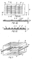
- Fig. 3 shows a wire mesh 6 of wires 5' of the first and wires 5" of a second plurality, wherein the wires 5', 5" of the first and second pluralities are usually running perpendicularly to each other.
- the wires 5" are, at least on the surfaces facing the wires 5', also covered with an alloy coating 2. However, if the amount of alloy material on the wires 5' of the first plurality is sufficient for a safe mechanical and electrical connection of the two pluralities of wires at the crossing points, the alloy coating on the wires 5"of the second plurality could be omitted.
- Fig. 4 shows the schematic view of a device for producing a film-type adhesive optically transparent electrode.
- the alloy-coated wires 5' are wound up on several rolls 7, the number of which equals the width of the PV cell divided by the required distances between the parallel running wires 5' of the first plurality. For example, at a width of the PV cell of 100 mm and a distance between the wires of 4 mm, 26 rolls 7 are required.
- the rolls 7 are fastened on an axis 8, so that it is possible to form parallel lines of wires 5', which are running through corresponding openings in a frame 9.
- the distance between the openings in the frame 9 is determined by the requested distance between the parallel wires 5'. Size and form of the openings in the frame 9 have to correspond to the size and form of the cross-sectional area of the wires 5'.
- the parallel wires 5' are disposed on a polymeric film 10, which is supplied from a drum 12.
- the surface of the film 10 facing the wires 5' is coated with a transparent adhesive 11.
- the overall width of the film 10, on which the wires 5'are placed exceeds the width of one or an array of several wafers 3, so that on each side of the film 10 a zone of 1.5 to 2 cm remains free of wires 5' (Fig. 5A).
- the film 10 is lead by the drum 12 over the surface of a rotatable roller 13 and is pulled by a drum 15, simultaneously pulling the wires 5'.
- the wires 5' are pressed on the film 10 by means of another roller 14 arranged above the rotatable roller 13.
- the film 10 is heated by the rollers 13 and 14, so that the adhesive 11 softens, the wires 5' immerse in the adhesive 11 and, after cooling down, remain fixed to the film 10 and embedded in the adhesive 11. It is recommended that the opposite side of the polymeric film should be primed by adhesive material to allow further PV cell encapsulation between protective layers.
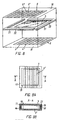
- Figs. 5A and 5B show in detail the result of this process, namely a transparent electrode 16.
- the wires 5' extending along the polymeric film 10 are embedded in the adhesive 11 and pressed onto the film 10. A part of the surface of the wires 5' is protruding from the surface of the adhesive 11.
- Fig. 5B on the left and right-hand other possible cross-sectional forms of the wires 5' are again depicted.
- a production device similar to that of Fig. 4 may be used for producing a polymeric film 10 with embedded wires 5' being transversely arranged to the initial direction of the film 10 (Figs. 5C, 5D).
- the width of the polymeric film 10 has hereby to correspond to the required length of a PV cell or PV module. After the wires 5' of the first plurality are embedded in the film 10, it may be cut in pieces transverse to the initial extension of the film 10.
- the distance of the wires 5' and/or 5" is not required to be uniform, i.e. the parallel wires 5' and/or 5" can be arranged in groups of two or more wires with different distances between the wires in each group and number of such groups.
- Fig. 6A shows an electrode 16 comprising the transparent polymeric film 10 and a wire mesh 6 of the wires 5' and 5" of the first and second pluralities. Only the wires 5" being more closely located to the polymeric film 10 are immersed in the adhesive 11 (see also Figs. 6B and 6C). The upper wires 5' coming into contact with the surface or surfaces of the wafer 3 are not, at least not completely, immersed in the adhesive 11 (during the production of this type of an electrode 16 the roll 7 carries a wire mesh 6, and frame 9 is not used (Fig.4)). Already at this point, the wires 5', 5" may be soldered together. However, usually this is done at the time of assembly of the electrode 16 and the wafer 3.
- the material must have a high ductility, good insulating characteristics, optical transparency and thermal stability, resistance to shrinkage and have a good adhesive ability.
- materials are cellophane®, rayon, acetate, fluororesin, polysulfone, epoxy resin, and polyamide resin.
- a suitable material to be used is also the transparent polymeric film Mylar®.
- Materials to be preferably used are those based on a fluoropolymer; for example the polyvinyl fluoride film Tedlar® and the modified ETFE fluoropolymer resin Tefzel®. These materials are used not only in photovoltaic industry but also for general purposes and for electrotechnical products for lamination purposes.
- a wide range of materials having a softening temperature ranging from about 90 - 110°C and having a good adhesion to preliminarily primed polymeric films and the surface of the wafer 3 are suitable as adhesive 11.
- Preferred materials are acrylic adhesive materials, rubber adhesive materials, silicon adhesive materials and polyvinyl ether adhesive materials as well as epoxy adhesive materials.
- Materials to be most preferably used are Ethylene Vinyl Acetate, for example, supplied by HI-SHEET INDUSTRIES, LTD and those supplied by Dupont: 68080 Polymethyl methacrylate, 68040 Methacrylate copolymer, 68070 Methacrylate copolymer.
- the adhesive layer 11 has to be sufficiently thick in order to provide for a reliable connection of the electrode with the wafer 3.
- the thickness of the adhesive layer should, however, not exceed the thickness of the wires 5', so that the part of the wires 5' protruding from the adhesive 11, which part is coated with the alloy 2 and is not immersed in the adhesive 11 can later on form a direct ohmic contact with the electrically conductive surface, of the wafer 3 (Figs. 5A, 5D, 6B, 6C).
- the polymeric film 10 has to be sufficiently thick, so that it is sufficiently stable when the adhesive 11 is applied and when it is pulled under pressure and heat when attaching the wires 5', 5". Simultaneously, it should be as thin as possible in order to achieve high elasticity and transparency for the light passing through it.
- the thickness of the polymeric film 11 ranges between 10 and 50 ⁇ m. As was mentioned before it is preferable if the opposite side of polymeric film is primed with adhesive material.
- Figs. 5 and 6 the polymeric film 10 is shown with the adhesive 11 and the wires 5' (or the mesh 6 with the wires 5', 5") with the alloy coating 2 protruding from the surface of the adhesive 11, forming a continuous or endless film-type optically transparent adhesive electrode 16.
- the electrode 16 of this invention may be applied for the production of PV cells and PV modules.
- different types of metallic rods or bars and connections are required in order to collect the current from the electrode 16 and transmit it further. It is hereby advisable to attach the metallic rods or bars to the electrode 16 by some drops of glue or by brief local heating, thus bonding or fixing the metallic rods or bars to the adhesive 11 of the electrode 16.
- the distance between the metallic bars and different types of connections has to be designed in such a way that there is enough space between the wafers 3 so that they will not come into direct electrical contact with the constructional elements when they thermally expand under up to 160 °C heating during the assembly of the wafer 3 and the electrode 16.
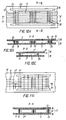
- Fig. 7 shows a drawn out depiction of a PV cell before its assembling by means of pressing and heating.
- Electrodes 16 are respectively disposed above and below the wafer 3. In a direction transverse to the longitudinal extension of the wires 5' of the electrodes 16, there are disposed at two opposite sides of the wafer 3 a first terminal bar 20 and a second terminal bar 22, which on their lower or upper sides, respectively, are provided with a coating 21 consisting of an electrically conductive alloy with a low melting point.
- the wires 5' of the upper electrode 16 are extending from the right border of the wafer 3 up to the left edge of the second terminal bar 22. In reverse, the wires 5' of the lower electrode 16 are extending from the left edge of the wafer 3 to the right edge of the first terminal bar 20.
- the wires 5' of the upper electrode 16 are in ohmic contact with the left, second terminal bar 22 and the upper surface of the wafer 3, while the wires 5' of the lower electrode 16 are in ohmic contact with the lower side of the terminal bar 20 and the lower side of the wafer 3.
- the electrically conductive alloys 2, 21 with a low melting point may be represented either by common solders or specially developed ones on the basis of different metals, like Ag, Bi, Cd, Ga, In, Pb, Sn, Ti, etc. It is also possible to use electroconductive material composed of organic adhesives with metallic or alloy particles.
- Fig. 8 shows a similar structure, however with angularly formed terminal bars 20, 22 and electrodes 16 with wires 5', 5" arranged in the form of a mesh 6.
- the mesh 6 of the lower electrode 16 is in ohmic contact with the right, first angularly formed terminal bar 20 and the lower side of the wafer 3, while the mesh 6 of the upper electrode 16 is in ohmic contact with the second angularly formed terminal bar 22 and the upper side of the wafer 3.
- Figs. 9A and 9B show a PV cell, wherein the terminal bars are configured in the form of a three-layered laminated frame 17, in the window of which the corresponding wafer 3 is accommodated.
- the wires 5' are running between two opposite sides of the frame 17, onto which sides they are soldered as a result of heating and pressing.
- the frame 17 comprises two metallic frames 18, between which there is disposed a preferably double-sided adhesive insulating film 19.
- a conductive alloy coating 21 is applied on the outer sides of the two frames 18, respectively. This coating may be omitted when the amount of the material on the wires 5' is sufficient for a reliable ohmic contact between the frame 17 and the wires 5'. In this case it is recommended that the frame 17 should be tinned.
- This embodiment is also suitable for use with an electrode 16 in the form of a mesh, wherein the wires 5" of the second plurality (not shown) are running perpendicularly to the wires 5' of the first plurality and are in ohmic contact with the corresponding sides of the frame 17 depicted in Fig. 9.
- the following embodiments illustrate how, with the help of the electrode 16 of this invention, which is produced in the form of an endless strip, an array of PV cells may be connected in series and parallel to each other thereby constituting PV modules.
- Figs. 10A, 10B and 10C show an endless electrode 16 with comb-like terminal bars 23, the longitudinal bars 24 of which outside the wires 5'are running in parallel to them in the direction of the longitudinal extension of the endless electrode 16.
- the longitudinal bars 24 are integrally connected with transversely running transverse bars 25 (the "teeth" of the comb), which from the one or the other direction, respectively, are protruding into the spaces between the wafers 3.
- the upper surfaces of the left transverse bars 25 are provided with an insulating film 19, while on the lower surface a coating 21 is applied consisting of an electrically conductive alloy.
- a coating 21 is applied consisting of an electrically conductive alloy.
- the insulating film 19 is deposited on the lower surface and the coating 21 consisting of a conductive alloy is deposited on the upper surface.
- Fig. 10C shows the cross section B-B of Fig. 10A.
- Figs. 11A and 11B show an embodiment, wherein the PV cells parallel connections similar to Figs. 9A and 9B are configured in the form of a three-layered frame 17, which is laminated from an endless array of metallic frames 18 arranged in series and an insulating polymeric film 19 arranged between these frames 18. On the outer sides of the frames 18 a conductive coating 21 melting at low temperatures is deposited. This coating 21 is in ohmic contact with the wires 5' and 5" of the electrode 16.
- the wafers 3 are positioned within the "windows" of frame 17 and the PV cells are connected in parallel to each other by means of the upper and lower electrodes 16.
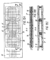
- Figs. 12 A and 12 B show a series connection of several PV cells.
- the terminal bars 25 running in transverse direction to the longitudinal extension of the electrode 16, with periodically interrupted wires 5', are provided with a coating 21 on their upper and lower sides, respectively.
- the wires 5' of the upper electrode 16 provide ohmic contact between the upper side of a terminal bar 25 and the upper side of the wafer 3 arranged on the right side thereof
- the wires 5' of the lower electrode 16 provide ohmic contact between the lower side of each terminal bar 25 and the lower side of the wafer 3 arranged on the left side thereof.
- Fig. 13 shows an endless electrode 16, wherein the PV cells' series connection is accomplished by means of U-shaped metallic terminal bars 26. Bars 24 of the terminal bars running in the longitudinal direction are in ohmic contact with the wires 5", and the transverse bars 25 thereof running in a transverse direction to the electrode 16 are in ohmic contact with the wires 5'.
- the wafers 3 are positioned within the space of the U-shaped metallic terminal bars 26 and between the upper and lower electrodes 16.
- Figs. 14A and 14B show an electrode 16 as it may be used for the PV cells' series connection as depicted on Figs. 12A and 12B and analogously for the arrangement of Fig. 13.
- the wires 5' are each interrupted by perforations 29, which include either only one wire 5' or several wires 5', respectively.
- the solidity of the electrode 16 remains better when the perforations 29 interrupt only one wire 5', compared with the case where several neighbouring wires are perforated. In the latter case it is recommended that a strip of transparent adhesive polymeric film (not shown) be applied on the perforated part of the electrode 16 in a direction transverse to the longitudinal extension of the electrode 16.
- the terminal bars 24 running in the longitudinal direction may also be interrupted, along with the wires 5'.
- the terminal bars 24 running in the longitudinal direction may also be interrupted, along with the wires 5'.
- the basic element of the arrangement according to Fig. 15 is a laminated three-layered double frame 27 comprising two metallic frames (preferably copper foil) 28 and an insulating film 19 provided between these frames.
- a step is provided in the central bar of double frame 27 and parallel thereto .
- the height of said step corresponds to the thickness of the metal foil, i.e. to about 0.2 to 0.3 mm (Figs. 15A, 15B, 15C).
- the metallic frames 28 are superposed in positions shifted with respect to each other, i.e. the left upper part of a metallic frame 28 is arranged above the right lower part of the left adjacent frame 28.
- the insulating film 19 provided between the two superposing metallic frames 28 of adjacent double frames 27 is bent at its ends in an upward or downward direction and extends up to the surface of the frame 27 construction.
- the wafers 3 are positioned within the "windows" of frames27.
- the wires 5' of the upper and lower perforated electrodes 16 are in ohmic contact with the surfaces of the wafer 3, and the respective left and right bars of each of the frame windows.
- the wires 5" are electrically connected with the wires 5' and the respective upper and lower bars of the frames.
- the surfaces of the metallic frames 28 in contact with the wires 5' are, if necessary, coated with an alloy coating 21 having a low melting point or are just tinned.
- Figs. 16A, 16B and 16C show a similar, but substantially simplified, construction wherein the non-perforated electrode 16 corresponds to that shown in Figs. 5C and 5D.
- longitudinal bars 32 with a step are utilized. These longitudinal bars 32 are lined up like the frames 28 as depicted on Fig. 15B and 15C.
- Fig. 17 shows in a drawn out depiction, representative of a whole array, two superposed metallic frames 28 with a step in the middle and arranged in positions shifted with respect to each other.
- the special feature of this arrangement is that the transverse bars 31 are spanning over the respective right lower windows, said bars 31 being integrally connected with the metallic frame 28.
- the bars 31 take over the function of the wires 5' of the lower electrode 16 of this invention, i.e. in the completed PV cell they are in ohmic contact with the respective lower surface of the wafer 3 located above them.
- simple frames 30 are provided at their ends, wherein the simple frame 30 provided for at the left end of the array is also provided with bars 31.
- the construction is completed by an upper electrode 16 with electrode meshes 6, the wires 5' of which are perforated and after heating and pressing are connected with the upper surface of the wafer 3 and frames 28 and 30.
- the lower electrode 16 has perforated wire 5" sections or wire 5" fields running in longitudinal direction, said wire sections or wire fields being connected in the completed PV cell with the bars 31 and the frame 30. Here they take over the function of the wires 5", i.e. of the wires being only indirectly connected with the lower surface of wafer 3.
- Fig. 18 shows an embodiment similar to that of Fig. 17 with the difference that instead of the lower electrode 16 a transparent polymeric film 10 is provided to which an adhesive 11 is applied.
- FIG. 19 an embodiment is shown similar to that depicted in Figs. 17 and 18.
- the upper electrode 16 has an uninterrupted mesh 6.
- This slot 33 runs parallel to the step. These slots 33 allow for the wires 5' of the upper electrode 16 to be cut throughout after assembly of the PV module. The width of the slot 33 is calculated in such a way that the wires 5' after perforation remain permanently interrupted and isolated from each other.
Landscapes
- Engineering & Computer Science (AREA)
- Condensed Matter Physics & Semiconductors (AREA)
- Physics & Mathematics (AREA)
- Electromagnetism (AREA)
- General Physics & Mathematics (AREA)
- Computer Hardware Design (AREA)
- Microelectronics & Electronic Packaging (AREA)
- Power Engineering (AREA)
- Life Sciences & Earth Sciences (AREA)
- Sustainable Development (AREA)
- Sustainable Energy (AREA)
- Photovoltaic Devices (AREA)
- Hybrid Cells (AREA)
Claims (19)
- Elektrode zum Kontaktieren einer Oberfläche eines fotovoltaischen Elements (Wafer 3), mit einem elektrisch isolierenden, optisch transparenten Film (10), mit einer auf eine Oberfläche des Films (10) aufgebrachten Kleberschicht (11), und mit einer ersten Gruppe im Wesentlichen paralleler, elektrisch leitfähiger Drähte (5'), die in die Klebstoffschicht (11) eingebettet sind, aus der Klebstoffschicht (11) mit einem Teil ihrer Oberfläche hervortreten und wenigstens auf der aus der Klebstoffschicht (11) heraustretenden Oberfläche mit einer Schicht (2) aus einer Legierung mit niedrigem Schmelzpunkt überzogen sind, zum Löten der Drähte (5') auf die Oberfläche des fotovoltaischen Elements wo die Drähte (5') in die Kleberschicht eingebettet sind, wobei die Drähte (5') der ersten Gruppe mit einer ersten Kontaktleiste (20) elektrisch verbunden sind.
- Elektrode nach Anspruch 1, wobei eine zweite Gruppe im Wesentlichen parallel zueinander verlaufender Drähte (5") zwischen dem transparenten Film (10) und den Drähten (5') der ersten Gruppe angeordnet ist, wobei die Drähte (5', 5") der ersten und zweiten Gruppe zusammen ein Gitter (6) bilden, und wobei die Drähte (5") der zweiten Gruppe mit einer zweiten Kontaktleiste (22) elektrisch verbunden sind.
- Elektrode nach Anspruch 2, wobei die erste und zweite Kontaktleiste (20, 22) elektrisch miteinander verbunden sind.
- Elektrode nach einem der vorstehenden Ansprüche, wobei die Kontaktleiste(n) (20, 22) an den jeweiligen Enden der Drähte (5', 5") angeordnet sind.
- Elektrode nach Anspruch 4, wobei die Kontaktleiste(n) (20, 22) an gegenüberliegenden Enden der Drähte der ersten oder der ersten und zweiten Gruppe von Drähten (5', 5") außerhalb der Kontur des fotovoltaischen Elements (Wafer 3) angeordnet sind, mit dessen Oberfläche die Drähte (5', 5") zu verbinden sind.
- Elektrode nach einem der Ansprüche 1 bis 5, wobei die ersten und zweiten Kontaktleisten (20, 22) zu einem Winkel miteinander verbunden sind (Fig. 8).
- Elektrode nach einem der Ansprüche 1 bis 5, wobei die Kontaktleisten (20, 22) als U-förmiger Rahmen ausgebildet sind, wobei die Drähte (5') einer der beiden Gruppen mit der Basis und die Drähte (5") der anderen Gruppe mit den freien Schenkeln des U verbunden sind (Fig. 13).
- Elektrode nach Anspruch 5, dadurch gekennzeichnet, dass die Kontaktleisten (32) sich über die Länge zweier nebeneinander angeordneter, zu verbindender fotovoltaischer Elemente (3) erstrecken und in ihrer Mitte mit einer Stufe versehen sind, so dass mehrere Kontaktleisten (32) zu einer Reihe zusammengefügt werden können, in der jeweils die eine Hälfte einer Kontaktleiste (32) unter bzw. über der unteren bzw. oberen Hälfte der benachbarten Kontaktleiste (32) liegt, wobei zwischen den Kontaktleisten (32) ein Isolierfilm (19) angeordnet ist (Fig. 16).
- Elektrode nach Anspruch 5, wobei die Kontaktleisten als geschlossener Rahmen (17) ausgebildet sind, dessen Öffnungsweite (Fenster) größer ist als die Abmessungen des entsprechenden fotovoltaischen Elements (3) (Fig. 9).
- Elektrode nach Anspruch 5, wobei die Kontaktleiste(n) als Doppelrahmen (17) mit zwei nebeneinanderliegenden Fenstern ausgebildet ist (sind), deren Öffnungsweite größer ist als die Abmessungen der entsprechenden fotovoltaischen Elemente (3).
- Elektrode nach Anspruch 9 oder 10, wobei der Rahmen (17) zwei metallische Rahmen (18) aufweist und zwischen ihnen ein Isolierfilm (19) ausgebildet ist.
- Elektrode nach Anspruch 10 oder 11, wobei im Mittelsteg des Doppelrahmens (17) eine Stufe ausgebildet ist, so dass mehrere Rahmen (17) zu einer Reihe zusammengefügt werden können, in der jeweils die eine Hälfte eines Doppelrahmens (17) unter bzw. über der unteren bzw. oberen Hälfte des benachbarten Doppelrahmens (17) liegt.
- Elektrode nach Anspruch 11 oder 12, wobei im mittleren Steg des Doppelrahmens (28) ein Schlitz (33) vorgesehen ist, der parallel zur Stufe verläuft, so dass die durchlaufenden Drähte (5', 5") der Elektrode (16) nach Fertigstellung eines PV-Moduls aufgetrennt werden können.
- Elektrode nach einem der Ansprüche 9 bis 13, wobei wenigstens ein Fenster des/der Rahmen(s) von metallischen Stegen (31) überspannt ist, die mit dem zugehörigen metallischen Rahmen (18) einteilig verbunden sind.
- Eine Mehrzahl von Elektroden nach einem der vorstehenden Ansprüche, wobei die Elektroden als endloses, durchgehendes Band ausgebildet sind, das sich entsprechend der Länge einer Reihe nebeneinander liegender, zur Bildung eines PV-Moduls zu verbindender fotovoltaischer Elemente (3) aufschneiden lässt, wobei die in Längsrichtung des Bandes verlaufenden Drähte (5', 5") in Abständen aufgetrennt sind, die den Abständen der PV-Zellen entsprechen (Fig. 14).
- Elektrodenband nach Anspruch 15, wobei längs wenigstens einer der Kanten des transparenten Films (10) eine endlose Kontaktleiste (22) vorgesehen ist.
- Elektrodenband nach Anspruch 16, wobei längs jeder Kante des transparenten Films (10) kammförmige Kontaktleisten (23) verlaufen, deren Zinken (25) jeweils von einer Seite zwischen zwei nebeneinander liegende fotovoltaische Elemente (3) über die Breite der Drähte (5') der ersten Gruppe hineinragen und wechselseitig in elektrischem Kontakt mit der Oberseite und Unterseite zugehöriger fotovoltaischer Elemente (3) liegen und von der anderen Oberfläche isoliert sind.
- PV-Zelle oder PV-Modul mit wenigstens einer Elektrode oder einem Elektrodenband nach einem der vorstehenden Ansprüche, mit einer bzw. mehreren fotovoltaischen Zellen (3) mit einer elektrisch leitfähigen, nicht reflektierenden, optisch transparenten Schicht (4) auf wenigstens einer ihrer Oberflächen, wobei die Drähte (5') der ersten Gruppe mit Hilfe der Legierung (2) auf die Schicht (4) und auf die jeweiligen Kontaktleisten (20) oder Kontaktrahmen (17) gelötet sind.
- PV-Zelle oder PV-Modul nach Anspruch 18, mit einer Elektrode (16) nach Anspruch 2, wobei die Drähte (5', 5") der ersten und zweiten Gruppe mittels der Legierung (2) an ihren Kreuzungspunkten und auf die jeweiligen Kontaktleisten oder Kontaktrahmen gebondet sind.
Priority Applications (2)
| Application Number | Priority Date | Filing Date | Title |
|---|---|---|---|
| SI200331121T SI1547158T1 (sl) | 2002-08-29 | 2003-08-21 | Elektroda za fotovoltaicne celice, fotovoltaicna celica in fotovoltaicni modul |
| CY20081100234T CY1107220T1 (el) | 2002-08-29 | 2008-02-28 | Ηλεκτροδιο για φωτοβολταϊκα στοιχεια, φωτοβολταϊκο στοιχειο και φωτοβολταϊκη μοναδα |
Applications Claiming Priority (3)
| Application Number | Priority Date | Filing Date | Title |
|---|---|---|---|
| DE10239845A DE10239845C1 (de) | 2002-08-29 | 2002-08-29 | Elektrode für fotovoltaische Zellen, fotovoltaische Zelle und fotovoltaischer Modul |
| DE10239845 | 2002-08-29 | ||
| PCT/CA2003/001278 WO2004021455A1 (en) | 2002-08-29 | 2003-08-21 | Electrode for photovoltaic cells, photovoltaic cell and photovoltaic module |
Publications (2)
| Publication Number | Publication Date |
|---|---|
| EP1547158A1 EP1547158A1 (de) | 2005-06-29 |
| EP1547158B1 true EP1547158B1 (de) | 2007-11-28 |
Family
ID=29594632
Family Applications (1)
| Application Number | Title | Priority Date | Filing Date |
|---|---|---|---|
| EP03790589A Expired - Lifetime EP1547158B1 (de) | 2002-08-29 | 2003-08-21 | Elektrode für fotovoltaische zellen, fotovoltaische zelle und fotovoltaisches modul |
Country Status (20)
| Country | Link |
|---|---|
| US (2) | US7432438B2 (de) |
| EP (1) | EP1547158B1 (de) |
| JP (2) | JP2005536894A (de) |
| KR (1) | KR101014393B1 (de) |
| CN (2) | CN100431175C (de) |
| AT (1) | ATE379849T1 (de) |
| AU (1) | AU2003258427B8 (de) |
| BR (1) | BRPI0313851B1 (de) |
| CA (1) | CA2496557C (de) |
| CY (1) | CY1107220T1 (de) |
| DE (2) | DE10239845C1 (de) |
| DK (1) | DK1547158T3 (de) |
| ES (1) | ES2297257T3 (de) |
| HK (2) | HK1077122A1 (de) |
| IL (1) | IL166854A (de) |
| MX (1) | MXPA05002321A (de) |
| PT (1) | PT1547158E (de) |
| SI (1) | SI1547158T1 (de) |
| WO (1) | WO2004021455A1 (de) |
| ZA (1) | ZA200501563B (de) |
Cited By (4)
| Publication number | Priority date | Publication date | Assignee | Title |
|---|---|---|---|---|
| WO2016156276A1 (en) * | 2015-03-30 | 2016-10-06 | Imec Vzw | Electrically contacting and interconnecting photovoltaic cells |
| EP3389099A1 (de) | 2017-04-14 | 2018-10-17 | Meyer Burger AG | Photovoltaikmodul, photovoltaischer verkapselungsstoff und verfahren zur herstellung eines photovoltaikmoduls |
| WO2019010542A1 (en) * | 2017-07-14 | 2019-01-17 | Commonwealth Scientific And Industrial Research Organisation | PHOTOVOLTAIC APPARATUS AND METHOD |
| IT202100009254A1 (it) | 2021-04-13 | 2022-10-13 | Fly Solartech Solutions S R L | Macchina e procedimento per la produzione di un elettrodo |
Families Citing this family (219)
| Publication number | Priority date | Publication date | Assignee | Title |
|---|---|---|---|---|
| US7732243B2 (en) | 1995-05-15 | 2010-06-08 | Daniel Luch | Substrate structures for integrated series connected photovoltaic arrays and process of manufacture of such arrays |
| US20080314433A1 (en) * | 1995-05-15 | 2008-12-25 | Daniel Luch | Substrate structures for integrated series connected photovoltaic arrays and process of manufacture of such arrays |
| US7635810B2 (en) * | 1999-03-30 | 2009-12-22 | Daniel Luch | Substrate and collector grid structures for integrated photovoltaic arrays and process of manufacture of such arrays |
| US8138413B2 (en) | 2006-04-13 | 2012-03-20 | Daniel Luch | Collector grid and interconnect structures for photovoltaic arrays and modules |
| US20090111206A1 (en) | 1999-03-30 | 2009-04-30 | Daniel Luch | Collector grid, electrode structures and interrconnect structures for photovoltaic arrays and methods of manufacture |
| US8664030B2 (en) | 1999-03-30 | 2014-03-04 | Daniel Luch | Collector grid and interconnect structures for photovoltaic arrays and modules |
| US7507903B2 (en) | 1999-03-30 | 2009-03-24 | Daniel Luch | Substrate and collector grid structures for integrated series connected photovoltaic arrays and process of manufacture of such arrays |
| US8076568B2 (en) | 2006-04-13 | 2011-12-13 | Daniel Luch | Collector grid and interconnect structures for photovoltaic arrays and modules |
| US8222513B2 (en) | 2006-04-13 | 2012-07-17 | Daniel Luch | Collector grid, electrode structures and interconnect structures for photovoltaic arrays and methods of manufacture |
| US7898054B2 (en) | 2000-02-04 | 2011-03-01 | Daniel Luch | Substrate structures for integrated series connected photovoltaic arrays and process of manufacture of such arrays |
| US7898053B2 (en) | 2000-02-04 | 2011-03-01 | Daniel Luch | Substrate structures for integrated series connected photovoltaic arrays and process of manufacture of such arrays |
| US8198696B2 (en) | 2000-02-04 | 2012-06-12 | Daniel Luch | Substrate structures for integrated series connected photovoltaic arrays and process of manufacture of such arrays |
| DE10239845C1 (de) | 2002-08-29 | 2003-12-24 | Day4 Energy Inc | Elektrode für fotovoltaische Zellen, fotovoltaische Zelle und fotovoltaischer Modul |
| US7838868B2 (en) | 2005-01-20 | 2010-11-23 | Nanosolar, Inc. | Optoelectronic architecture having compound conducting substrate |
| US7732229B2 (en) | 2004-09-18 | 2010-06-08 | Nanosolar, Inc. | Formation of solar cells with conductive barrier layers and foil substrates |
| US8927315B1 (en) | 2005-01-20 | 2015-01-06 | Aeris Capital Sustainable Ip Ltd. | High-throughput assembly of series interconnected solar cells |
| US7622666B2 (en) * | 2005-06-16 | 2009-11-24 | Soliant Energy Inc. | Photovoltaic concentrator modules and systems having a heat dissipating element located within a volume in which light rays converge from an optical concentrating element towards a photovoltaic receiver |
| US20070089777A1 (en) * | 2005-10-04 | 2007-04-26 | Johnson Richard L Jr | Heatsink for concentrating or focusing optical/electrical energy conversion systems |
| US20070144577A1 (en) * | 2005-12-23 | 2007-06-28 | Rubin George L | Solar cell with physically separated distributed electrical contacts |
| JP4642662B2 (ja) * | 2006-01-16 | 2011-03-02 | キヤノン株式会社 | 光起電力素子 |
| CN101375112A (zh) | 2006-01-17 | 2009-02-25 | 索利安特能源公司 | 用于光学聚光器的混合式主光学部件 |
| US7498508B2 (en) | 2006-02-24 | 2009-03-03 | Day4 Energy, Inc. | High voltage solar cell and solar cell module |
| JP4755246B2 (ja) * | 2006-03-31 | 2011-08-24 | パイオニア株式会社 | 低抵抗基板の作製方法 |
| US9006563B2 (en) | 2006-04-13 | 2015-04-14 | Solannex, Inc. | Collector grid and interconnect structures for photovoltaic arrays and modules |
| US9236512B2 (en) | 2006-04-13 | 2016-01-12 | Daniel Luch | Collector grid and interconnect structures for photovoltaic arrays and modules |
| US8884155B2 (en) | 2006-04-13 | 2014-11-11 | Daniel Luch | Collector grid and interconnect structures for photovoltaic arrays and modules |
| US8729385B2 (en) | 2006-04-13 | 2014-05-20 | Daniel Luch | Collector grid and interconnect structures for photovoltaic arrays and modules |
| US8822810B2 (en) | 2006-04-13 | 2014-09-02 | Daniel Luch | Collector grid and interconnect structures for photovoltaic arrays and modules |
| US9865758B2 (en) | 2006-04-13 | 2018-01-09 | Daniel Luch | Collector grid and interconnect structures for photovoltaic arrays and modules |
| US20070283996A1 (en) * | 2006-06-13 | 2007-12-13 | Miasole | Photovoltaic module with insulating interconnect carrier |
| US20070283997A1 (en) * | 2006-06-13 | 2007-12-13 | Miasole | Photovoltaic module with integrated current collection and interconnection |
| US20080053519A1 (en) * | 2006-08-30 | 2008-03-06 | Miasole | Laminated photovoltaic cell |
| DE102006041046A1 (de) * | 2006-09-01 | 2008-03-06 | Cis Solartechnik Gmbh & Co. Kg | Solarzelle, Verfahren zur Herstellung von Solarzellen sowie elektrische Leiterbahn |
| US20080083448A1 (en) * | 2006-09-29 | 2008-04-10 | Borden Peter G | Interconnect for thin film photovoltaic modules |
| WO2008048478A2 (en) * | 2006-10-13 | 2008-04-24 | Soliant Energy, Inc. | Sun sensor assembly and related method of using |
| US20080092944A1 (en) * | 2006-10-16 | 2008-04-24 | Leonid Rubin | Semiconductor structure and process for forming ohmic connections to a semiconductor structure |
| DE102006052018A1 (de) * | 2006-11-03 | 2008-05-15 | Fraunhofer-Gesellschaft zur Förderung der angewandten Forschung e.V. | Solarzelle und Solarzellenmodul mit verbesserten Rückseiten-Elektroden sowie Verfahren und Herstellung |
| US20080142071A1 (en) * | 2006-12-15 | 2008-06-19 | Miasole | Protovoltaic module utilizing a flex circuit for reconfiguration |
| US20090000612A1 (en) * | 2007-05-04 | 2009-01-01 | Hines Braden E | Apparatuses and methods for shaping reflective surfaces of optical concentrators |
| US20080290368A1 (en) * | 2007-05-21 | 2008-11-27 | Day4 Energy, Inc. | Photovoltaic cell with shallow emitter |
| WO2008153690A1 (en) * | 2007-05-22 | 2008-12-18 | Miasole | High rate sputtering apparatus and method |
| US8697980B2 (en) * | 2007-06-19 | 2014-04-15 | Hanergy Holding Group Ltd. | Photovoltaic module utilizing an integrated flex circuit and incorporating a bypass diode |
| US20090014058A1 (en) * | 2007-07-13 | 2009-01-15 | Miasole | Rooftop photovoltaic systems |
| US20090014057A1 (en) * | 2007-07-13 | 2009-01-15 | Miasole | Photovoltaic modules with integrated devices |
| US20090014049A1 (en) * | 2007-07-13 | 2009-01-15 | Miasole | Photovoltaic module with integrated energy storage |
| EP2198367A1 (de) * | 2007-08-31 | 2010-06-23 | Applied Materials, Inc. | Photovoltaik-produktionslinie |
| US20100047954A1 (en) * | 2007-08-31 | 2010-02-25 | Su Tzay-Fa Jeff | Photovoltaic production line |
| JP2009117742A (ja) * | 2007-11-09 | 2009-05-28 | Bridgestone Corp | 太陽電池用電極フィルム、これを用いた太陽電池の製造方法、並びに太陽電池 |
| JP4990738B2 (ja) * | 2007-11-09 | 2012-08-01 | 株式会社ブリヂストン | 太陽電池の製造方法 |
| TW200939509A (en) * | 2007-11-19 | 2009-09-16 | Applied Materials Inc | Crystalline solar cell metallization methods |
| JP2011503910A (ja) * | 2007-11-19 | 2011-01-27 | アプライド マテリアルズ インコーポレイテッド | パターン付きエッチング剤を用いた太陽電池コンタクト形成プロセス |
| JP2011507275A (ja) * | 2007-12-11 | 2011-03-03 | エバーグリーン ソーラー, インコーポレイテッド | 微細なフィンガーを有する光起電力性パネルおよび光起電力性電池ならびにこれらの製造方法 |
| US20100000602A1 (en) * | 2007-12-11 | 2010-01-07 | Evergreen Solar, Inc. | Photovoltaic Cell with Efficient Finger and Tab Layout |
| US20090199894A1 (en) * | 2007-12-14 | 2009-08-13 | Miasole | Photovoltaic devices protected from environment |
| MX2010006881A (es) * | 2007-12-18 | 2010-12-06 | Day4 Energy Inc | Modulo fotovoltaico con acceso marginal a filamentos pv, metodo, aparato, y sistema de interconexion. |
| US20090183764A1 (en) * | 2008-01-18 | 2009-07-23 | Tenksolar, Inc | Detachable Louver System |
| US8212139B2 (en) | 2008-01-18 | 2012-07-03 | Tenksolar, Inc. | Thin-film photovoltaic module |
| US8933320B2 (en) | 2008-01-18 | 2015-01-13 | Tenksolar, Inc. | Redundant electrical architecture for photovoltaic modules |
| US8748727B2 (en) | 2008-01-18 | 2014-06-10 | Tenksolar, Inc. | Flat-plate photovoltaic module |
| US20090188603A1 (en) * | 2008-01-25 | 2009-07-30 | Applied Materials, Inc. | Method and apparatus for controlling laminator temperature on a solar cell |
| CN102089892B (zh) * | 2008-02-27 | 2013-02-13 | 应用材料公司 | 用于在太阳能电池上形成电连接的设备与方法 |
| US7908743B2 (en) * | 2008-02-27 | 2011-03-22 | Applied Materials, Inc. | Method for forming an electrical connection |
| US20100043863A1 (en) * | 2008-03-20 | 2010-02-25 | Miasole | Interconnect assembly |
| US8912429B2 (en) * | 2008-03-20 | 2014-12-16 | Hanergy Holding Group Ltd. | Interconnect assembly |
| US20110197947A1 (en) * | 2008-03-20 | 2011-08-18 | Miasole | Wire network for interconnecting photovoltaic cells |
| JP5094509B2 (ja) * | 2008-03-31 | 2012-12-12 | 三洋電機株式会社 | 太陽電池モジュール |
| DE102008020749A1 (de) * | 2008-04-22 | 2009-10-29 | Cis Solartechnik Gmbh & Co. Kg | Verfahren zur Herstellung einer Solarzelle |
| US20090283137A1 (en) * | 2008-05-15 | 2009-11-19 | Steven Thomas Croft | Solar-cell module with in-laminate diodes and external-connection mechanisms mounted to respective edge regions |
| AU2009246864A1 (en) | 2008-05-16 | 2009-11-19 | Emcore Corporation | Solar systems that include one or more shade-tolerant wiring schemes |
| DE102008030262A1 (de) * | 2008-06-18 | 2009-12-24 | Gebr. Schmid Gmbh & Co. | Solarzelle und Verfahren zur Herstellung einer Solarzelle |
| JP5436805B2 (ja) * | 2008-07-04 | 2014-03-05 | 三洋電機株式会社 | 太陽電池モジュール |
| WO2010009297A2 (en) * | 2008-07-16 | 2010-01-21 | Applied Materials, Inc. | Hybrid heterojunction solar cell fabrication using a doping layer mask |
| CN102105999A (zh) | 2008-07-28 | 2011-06-22 | 达伊4能量有限公司 | 用低温精密回蚀和钝化过程制备的具有选择性发射极的晶体硅光伏电池 |
| US20100037933A1 (en) * | 2008-08-12 | 2010-02-18 | Harold John Hovel | Solar cell panels and method of fabricating same |
| TW201027766A (en) * | 2008-08-27 | 2010-07-16 | Applied Materials Inc | Back contact solar cells using printed dielectric barrier |
| JP2010067968A (ja) * | 2008-09-11 | 2010-03-25 | Komax Holding Ag | 太陽素子に対して細長導体を付着するための方法および装置 |
| JP5064353B2 (ja) * | 2008-10-27 | 2012-10-31 | シャープ株式会社 | 太陽電池装置、携帯電子機器、並びに全地球測位システム装置 |
| US9059351B2 (en) | 2008-11-04 | 2015-06-16 | Apollo Precision (Fujian) Limited | Integrated diode assemblies for photovoltaic modules |
| US8586857B2 (en) * | 2008-11-04 | 2013-11-19 | Miasole | Combined diode, lead assembly incorporating an expansion joint |
| US20100122730A1 (en) * | 2008-11-17 | 2010-05-20 | Corneille Jason S | Power-loss-inhibiting current-collector |
| DE102008043833B4 (de) * | 2008-11-18 | 2016-03-10 | Maximilian Scherff | Solarzellensystem, Solarmodul und Verfahren zur elektrischen Verschaltung rückseitenkontaktierter Solarzellen |
| DE202008016139U1 (de) * | 2008-12-08 | 2010-04-29 | Usk Karl Utz Sondermaschinen Gmbh | Solarzellenverbund |
| US20100206370A1 (en) * | 2009-02-18 | 2010-08-19 | Qualcomm Incorporated | Photovoltaic Cell Efficiency Using Through Silicon Vias |
| WO2010096833A2 (en) * | 2009-02-23 | 2010-08-26 | Tenksolar, Inc. | Highly efficient renewable energy system |
| US20120027994A1 (en) * | 2009-03-17 | 2012-02-02 | Konica Minolta Holdings, Inc. | Transparent conductive film and method for manufacturing transparent conductive film |
| DE202009006542U1 (de) | 2009-05-05 | 2009-07-23 | Feindrahtwerk Adolf Edelhoff Gmbh & Co. Kg | Elektrisches Kontaktierungselement für photovoltaische Zellen |
| DE102009020029A1 (de) | 2009-05-05 | 2010-11-11 | Feindrahtwerk Adolf Edelhoff Gmbh & Co. Kg | Elektrisches Kontaktierungselement für photovoltaische Zellen |
| US8247243B2 (en) | 2009-05-22 | 2012-08-21 | Nanosolar, Inc. | Solar cell interconnection |
| EP2438632A4 (de) * | 2009-06-03 | 2014-01-22 | First Solar Inc | Selbstreinigendes photovoltaikmodul |
| JP5380166B2 (ja) * | 2009-06-08 | 2014-01-08 | 株式会社アルバック | 結晶系太陽電池セル及びその製造方法 |
| JP5573372B2 (ja) * | 2009-06-11 | 2014-08-20 | 大日本印刷株式会社 | 有機薄膜太陽電池およびその製造方法 |
| IN2012DN00387A (de) | 2009-06-15 | 2015-08-21 | Tenksolar Inc | |
| WO2011014792A2 (en) * | 2009-07-30 | 2011-02-03 | Evergreen Solar, Inc. | Photovoltaic cell with semiconductor fingers |
| CH701679A1 (de) | 2009-08-19 | 2011-02-28 | Cells S A | Vorrichtung und Verfahren zur Kontaktierung von Siliziumsolarzellen. |
| US8574949B2 (en) * | 2009-09-20 | 2013-11-05 | Intermolecular, Inc. | Methods of building crystalline silicon solar cells for use in combinatorial screening |
| US8227723B2 (en) * | 2009-10-19 | 2012-07-24 | Applied Materials, Inc. | Solder bonding method and apparatus |
| US20110146786A1 (en) * | 2009-12-23 | 2011-06-23 | First Solar, Inc. | Photovoltaic module interlayer |
| US8759664B2 (en) | 2009-12-28 | 2014-06-24 | Hanergy Hi-Tech Power (Hk) Limited | Thin film solar cell strings |
| EP2348539B1 (de) | 2010-01-19 | 2019-05-29 | SolarWorld Industries GmbH | Photoelementelektrode und Verfahren zum elektrischen Anschließen eines Photoelements |
| US9773933B2 (en) | 2010-02-23 | 2017-09-26 | Tenksolar, Inc. | Space and energy efficient photovoltaic array |
| WO2011105538A1 (ja) * | 2010-02-25 | 2011-09-01 | 産機電業株式会社 | シリコン粉末を用いた太陽電池セルの製造方法 |
| DE102010016476B4 (de) | 2010-04-16 | 2022-09-29 | Meyer Burger (Germany) Gmbh | Verfahren zum Aufbringen von Kontaktdrähten auf eine Oberfläche einer Photovoltaikzelle, Photovoltaikzelle, Photovoltaikmodul, Anordnung zum Aufbringen von Kontaktdrähten auf eine Oberfläche einer Photovoltaikzelle |
| DE102010016675A1 (de) | 2010-04-28 | 2011-11-03 | Solarworld Innovations Gmbh | Photovoltaikmodul, Verfahren zum elektrischen Verbinden einer Mehrzahl von Photovoltaikzellen, und Einrichtung zum elektrischen Verbinden einer Mehrzahl von Photovoltaikzellen |
| US9061344B1 (en) | 2010-05-26 | 2015-06-23 | Apollo Precision (Fujian) Limited | Apparatuses and methods for fabricating wire current collectors and interconnects for solar cells |
| EP2577740B1 (de) | 2010-05-28 | 2018-11-14 | SolarWorld Industries GmbH | Verfahren zum kontaktieren und verschalten von solarzellen und damit hergestellter solarzellenverbund |
| DE102010017180A1 (de) | 2010-06-01 | 2011-12-01 | Solarworld Innovations Gmbh | Solarzelle, Solarmodul, und Verfahren zum Verdrahten einer Solarzelle, und Kontaktdraht |
| US9299861B2 (en) | 2010-06-15 | 2016-03-29 | Tenksolar, Inc. | Cell-to-grid redundandt photovoltaic system |
| JPWO2012014806A1 (ja) * | 2010-07-30 | 2013-09-12 | 三洋電機株式会社 | 太陽電池の製造方法 |
| WO2012021650A2 (en) | 2010-08-10 | 2012-02-16 | Tenksolar, Inc. | Highly efficient solar arrays |
| EP2614532B1 (de) | 2010-09-07 | 2015-08-05 | Dow Global Technologies LLC | Verbesserte pv-zellenanordnung |
| US20130167910A1 (en) | 2010-09-17 | 2013-07-04 | Dow Global Technologies Llc | Photovoltaic cell assembly and method |
| JP6115135B2 (ja) * | 2010-09-29 | 2017-04-19 | 日立化成株式会社 | 太陽電池モジュール |
| US10026859B2 (en) * | 2010-10-04 | 2018-07-17 | Beijing Apollo Ding Rong Solar Technology Co., Ltd. | Small gauge wire solar cell interconnect |
| WO2012051695A1 (en) * | 2010-10-18 | 2012-04-26 | Day4 Energy Inc. | Testing apparatus for photovoltaic cells |
| WO2012052542A1 (en) | 2010-10-21 | 2012-04-26 | Tag Hammam | Arrangement in a solar panel |
| US8956888B2 (en) | 2010-11-03 | 2015-02-17 | Apollo Precision Fujian Limited | Photovoltaic device and method and system for making photovoltaic device |
| KR101552779B1 (ko) * | 2010-12-06 | 2015-09-11 | 사카모토 준 | 패널, 패널의 제조방법, 태양전지 모듈, 인쇄장치 및 인쇄방법 |
| TW201234626A (en) * | 2011-01-13 | 2012-08-16 | Intevac Inc | Non-contacting bus bars for solar cells and methods of making non-contacting bus bars |
| DE102011000753A1 (de) * | 2011-02-15 | 2012-08-16 | Solarworld Innovations Gmbh | Solarzelle, Solarmodul und Verfahren zum Herstellen einer Solarzelle |
| DE102011001061B4 (de) * | 2011-03-03 | 2017-10-05 | Solarworld Innovations Gmbh | Solarzellenverbinder-Elektrode, Solarzellenmodul und Verfahren zum elektrischen Verbinden mehrerer Solarzellen |
| DE102011014795B4 (de) | 2011-03-15 | 2021-05-06 | Hegla Boraident Gmbh & Co. Kg | Verfahren zum Herstellen von flexiblen Dünnschicht-Solarzellen |
| JP5798772B2 (ja) * | 2011-03-25 | 2015-10-21 | デクセリアルズ株式会社 | 太陽電池モジュール、太陽電池モジュールの製造方法、タブ線 |
| US8951824B1 (en) | 2011-04-08 | 2015-02-10 | Apollo Precision (Fujian) Limited | Adhesives for attaching wire network to photovoltaic cells |
| CN102786883A (zh) | 2011-05-17 | 2012-11-21 | 旺能光电股份有限公司 | 电极胶带和太阳能电池模块及其制作方法 |
| TWI433331B (zh) | 2011-05-17 | 2014-04-01 | Neo Solar Power Corp | 電極膠帶之製作機台 |
| EP2528097A1 (de) | 2011-05-27 | 2012-11-28 | Nederlandse Organisatie voor toegepast -natuurwetenschappelijk onderzoek TNO | Photovoltaische Vorrichtung und Verfahren zu ihrer Herstellung |
| NL2006966C2 (en) | 2011-06-17 | 2012-12-18 | Stichting Energie | Photovoltaic system and connector for a photovoltaic cell with interdigitated contacts. |
| JP5903550B2 (ja) * | 2011-07-28 | 2016-04-13 | パナソニックIpマネジメント株式会社 | 太陽電池、太陽電池モジュール、太陽電池の製造方法 |
| WO2013030991A1 (ja) * | 2011-08-31 | 2013-03-07 | 三洋電機株式会社 | 太陽電池及びその製造方法 |
| CN102983785A (zh) * | 2011-09-02 | 2013-03-20 | 杜邦太阳能有限公司 | 光电转换系统 |
| WO2013048758A2 (en) | 2011-09-29 | 2013-04-04 | Dow Global Technologies Llc | Photovoltaic cell interconnect |
| US20140352753A1 (en) | 2011-09-29 | 2014-12-04 | Dow Global Technologies Llc | Photovoltaic cell interconnect |
| US8497153B2 (en) | 2011-10-31 | 2013-07-30 | E I Du Pont De Nemours And Company | Integrated back-sheet for back contact photovoltaic module |
| WO2013082091A2 (en) | 2011-11-29 | 2013-06-06 | Dow Global Technologies Llc | Method of forming a photovoltaic cell |
| CN103975447B (zh) | 2011-12-08 | 2017-04-12 | 陶氏环球技术有限责任公司 | 形成光伏电池的方法 |
| US9306103B2 (en) | 2011-12-22 | 2016-04-05 | E I Du Pont De Nemours And Company | Back contact photovoltaic module with integrated circuitry |
| WO2013091725A1 (en) * | 2011-12-23 | 2013-06-27 | Aurubis Ag | A conductor spool, a method for manufacturing a solar cell and a solar cell |
| CN104011882A (zh) | 2012-01-12 | 2014-08-27 | 应用材料公司 | 制造太阳能电池装置的方法 |
| WO2013106896A1 (en) * | 2012-01-17 | 2013-07-25 | Day4 Energy Inc. | Photovoltaic module with cell assemblies bearing adhesive for securing the assemblies in the module |
| IN2014KN01621A (de) | 2012-02-22 | 2015-10-23 | Muehlbauer Ag | |
| DE102012003455A1 (de) | 2012-02-22 | 2013-08-22 | Mühlbauer Ag | Verfahren und Vorrichtung zur Herstellung eines Solarmoduls und ein Solarmodul mit flexiblen Dünnschicht-Solarzellen |
| US9385254B2 (en) | 2012-04-17 | 2016-07-05 | Hanergy Hi-Tech Power (Hk) Limited | Integrated thin film solar cell interconnection |
| ITTO20120095U1 (it) | 2012-05-22 | 2013-11-23 | Domenico Gustavo Gioco | Pannello fotovoltaico flessibile. |
| DE102012017564B4 (de) * | 2012-09-05 | 2018-10-11 | Universität Konstanz | Vorrichtung zur nicht-permanenten elektrischen Kontaktierung von Solarzellen zur Messung elektrischer Eigenschaften |
| JP6050661B2 (ja) * | 2012-11-21 | 2016-12-21 | 長州産業株式会社 | 光発電装置の製造方法 |
| US9362433B2 (en) | 2013-01-28 | 2016-06-07 | Hanergy Hi-Tech Power (Hk) Limited | Photovoltaic interconnect systems, devices, and methods |
| KR102043425B1 (ko) * | 2013-03-06 | 2019-11-12 | 엘지전자 주식회사 | 태양 전지 측정 장치 |
| US8569096B1 (en) | 2013-03-13 | 2013-10-29 | Gtat Corporation | Free-standing metallic article for semiconductors |
| US8936709B2 (en) | 2013-03-13 | 2015-01-20 | Gtat Corporation | Adaptable free-standing metallic article for semiconductors |
| US8916038B2 (en) | 2013-03-13 | 2014-12-23 | Gtat Corporation | Free-standing metallic article for semiconductors |
| DE102013204814A1 (de) | 2013-03-19 | 2014-09-25 | Robert Bosch Gmbh | Fotovoltaik-Modul und Verfahren zur Herstellung eines Fotovoltaik-Moduls |
| AU2014239493A1 (en) | 2013-03-19 | 2015-10-29 | Choshu Industry Co., Ltd. | Photovoltaic element and manufacturing method therefor |
| CN103325875A (zh) * | 2013-06-23 | 2013-09-25 | 深圳市华光达科技有限公司 | 一种新型太阳能电池片的电流汇集装置及其制备工艺 |
| CN103500773A (zh) * | 2013-09-16 | 2014-01-08 | 深圳市索阳新能源科技有限公司 | 一种新型高效的背接触式太阳能发电组件及其制造方法 |
| DE102013219526B4 (de) | 2013-09-27 | 2022-10-13 | Meyer Burger (Germany) Gmbh | Solarzellenverbund mit Verbindungselement und Verfahren zum Herstellen eines Solarzellenverbunds |
| CN105612056A (zh) | 2013-10-15 | 2016-05-25 | 梅耶博格公司 | 用于形成层压板的方法和系统 |
| US9921261B2 (en) | 2013-10-17 | 2018-03-20 | Kla-Tencor Corporation | Method and apparatus for non-contact measurement of sheet resistance and shunt resistance of p-n junctions |
| DE102014200956A1 (de) * | 2013-12-20 | 2015-06-25 | Fraunhofer-Gesellschaft zur Förderung der angewandten Forschung e.V. | Photovoltaische Zelle, Photovoltaikmodul sowie dessen Herstellung und Verwendung |
| US10672927B2 (en) * | 2014-06-20 | 2020-06-02 | Merlin Solar Technologies, Inc. | Photovoltaic cell having a coupled expanded metal article |
| CN105322036B (zh) * | 2014-07-17 | 2017-06-23 | 英属开曼群岛商精曜有限公司 | 太阳能模块及其制造方法 |
| DE102014112650A1 (de) * | 2014-09-03 | 2016-03-03 | Hanwha Q Cells Gmbh | Solarmodul-Rückseitenverkapselungselement und Solarmodul |
| EP2993210A1 (de) | 2014-09-03 | 2016-03-09 | Specialized Technology Resources Espana, S.A. | Einkapselungsfilm für ein Photovoltaikmodul |
| EP3002792B1 (de) * | 2014-09-30 | 2016-12-21 | LG Electronics Inc. | Solarzelle und solarzellenplatte damit |
| US10529868B2 (en) | 2014-10-31 | 2020-01-07 | Byd Company Limited | Solar cell array, solar cell module and manufacturing method thereof |
| WO2016065935A1 (en) * | 2014-10-31 | 2016-05-06 | Byd Company Limited | Solar cell module and manufacturing method thereof |
| CN105576057B (zh) * | 2014-10-31 | 2018-06-26 | 比亚迪股份有限公司 | 太阳能电池组件及其制备方法 |
| CN106206765B (zh) * | 2014-10-31 | 2018-02-09 | 比亚迪股份有限公司 | 太阳能电池片阵列、太阳能电池组件及其制备方法 |
| DE102014118332A1 (de) * | 2014-12-10 | 2016-06-16 | Solarworld Innovations Gmbh | Photovoltaikmodul |
| DE112015005808T5 (de) * | 2014-12-26 | 2017-10-05 | Panasonic Intellectual Property Management Co., Ltd. | Solarzellenmodul |
| EP3046151B1 (de) * | 2015-01-16 | 2019-04-03 | Somont GmbH | Verfahren und Vorrichtung zur Herstellung einer Zwischenverbinderanordnung |
| EP3051595A1 (de) | 2015-01-29 | 2016-08-03 | Meyer Burger AG | Verfahren und Vorrichtung zur Herstellung eines Zwischenverbinders für Solarzellen und ein derartiger Zwischenverbinder |
| JP2018056145A (ja) * | 2015-02-06 | 2018-04-05 | 長州産業株式会社 | 光発電モジュール |
| CN107408593B (zh) * | 2015-02-06 | 2022-10-14 | 三井-陶氏聚合化学株式会社 | 配线片材、结构体及光发电模块 |
| KR101680037B1 (ko) | 2015-07-28 | 2016-12-12 | 엘지전자 주식회사 | 태양 전지 및 이를 포함하는 태양 전지 패널 |
| KR20170017776A (ko) * | 2015-08-05 | 2017-02-15 | 엘지전자 주식회사 | 태양 전지 패널용 리본 및 이의 제조 방법, 그리고 태양 전지 패널 |
| KR101661859B1 (ko) * | 2015-09-09 | 2016-09-30 | 엘지전자 주식회사 | 태양 전지 모듈 및 그 제조 방법 |
| CN106558631B (zh) * | 2015-09-18 | 2020-05-12 | 上海太阳能工程技术研究中心有限公司 | 无主栅双面电池组件及其制作工艺 |
| US10840394B2 (en) * | 2015-09-25 | 2020-11-17 | Total Marketing Services | Conductive strip based mask for metallization of semiconductor devices |
| ES2772256T3 (es) | 2015-11-06 | 2020-07-07 | Meyer Burger Switzerland Ag | Láminas conductoras de polímero, celdas solares y métodos para producirlos |
| CN105576046B (zh) * | 2015-12-15 | 2017-08-11 | 黄河水电光伏产业技术有限公司 | 一种用于太阳能电池的无主栅焊带的制备方法 |
| EP3449510B1 (de) * | 2016-04-29 | 2023-11-08 | AGC Glass Europe | Anordnung |
| US10128391B2 (en) | 2016-06-22 | 2018-11-13 | Beijing Apollo Ding Rong Solar Technology Co., Ltd. | Photovoltaic module with flexible wire interconnection |
| CN106393815B (zh) * | 2016-08-31 | 2018-04-06 | 西安泰力松新材料股份有限公司 | 一种金属丝/膜复合机及其控制装置和方法 |
| HUP1700044A2 (en) | 2017-01-31 | 2018-12-28 | Ecosolifer Invest Ag | Solar cell with improved electrodes and solar module composed of such cells |
| CN109004041B (zh) * | 2017-06-06 | 2020-04-28 | 清华大学 | 太阳能电池 |
| FR3067519B1 (fr) * | 2017-06-08 | 2019-07-26 | Centre National D'etudes Spatiales | Panneau solaire comportant notamment une structure et au moins deux cellules photovoltaiques |
| DE102017216528A1 (de) * | 2017-09-19 | 2019-03-21 | Continental Automotive Gmbh | Schutzfolie für Solarzelle, Solarmodul mit der Schutzfolie, Verfahren zum Herstellen der Solarfolie und des Solarmoduls |
| DE102017122530B4 (de) | 2017-09-28 | 2023-02-23 | Helmholtz-Zentrum Berlin für Materialien und Energie Gesellschaft mit beschränkter Haftung | Photovoltaikmodul mit auf der Rückseite ineinandergreifenden Kontakten |
| RU2671912C1 (ru) * | 2017-11-27 | 2018-11-07 | Общество с ограниченной ответственностью "НТЦ тонкопленочных технологий в энергетике", ООО "НТЦ ТПТ" | Электрод для контактирования фотоэлектрических преобразователей |
| FR3074360B1 (fr) * | 2017-11-30 | 2019-12-27 | Commissariat A L'energie Atomique Et Aux Energies Alternatives | Procede d'interconnexion de cellules photovoltaiques avec une electrode pourvue de nanofils metalliques |
| FR3074963B1 (fr) * | 2017-12-07 | 2022-08-12 | Commissariat Energie Atomique | Module photovoltaique comportant des cellules photovoltaiques interconnectees par des elements d'interconnexion |
| CN107978890B (zh) * | 2018-01-03 | 2024-02-13 | 菲尼克斯亚太电气(南京)有限公司 | 一种平方台阶式螺栓光伏端子 |
| CN108110080A (zh) * | 2018-01-10 | 2018-06-01 | 广东汉能薄膜太阳能有限公司 | 一种太阳能电极结构及使用该电极结构的太阳能电池 |
| US10490682B2 (en) | 2018-03-14 | 2019-11-26 | National Mechanical Group Corp. | Frame-less encapsulated photo-voltaic solar panel supporting solar cell modules encapsulated within multiple layers of optically-transparent epoxy-resin materials |
| WO2019191689A1 (en) | 2018-03-29 | 2019-10-03 | Sunpower Corporation | Wire-based metallization and stringing for solar cells |
| CN110717364B (zh) * | 2018-07-13 | 2023-09-22 | 中兴通讯股份有限公司 | 玻璃盖板、终端、指纹识别方法、装置及存储介质 |
| JP2021193695A (ja) | 2018-09-28 | 2021-12-23 | パナソニック株式会社 | 太陽電池モジュールの製造方法および太陽電池モジュール |
| KR20200039184A (ko) * | 2018-10-05 | 2020-04-16 | 엘지전자 주식회사 | 태양 전지 패널 |
| JP2020088133A (ja) * | 2018-11-22 | 2020-06-04 | パナソニック株式会社 | 太陽電池モジュール |
| JP2020107758A (ja) | 2018-12-27 | 2020-07-09 | パナソニック株式会社 | 太陽電池モジュール |
| US11271126B2 (en) | 2019-03-21 | 2022-03-08 | Beijing Apollo Ding Rong Solar Technology Co., Ltd. | Photovoltaic panels with folded panel edges and methods of forming the same |
| NL2022801B1 (nl) * | 2019-03-25 | 2020-10-02 | Lusoco B V | Inrichting voor het winnen van energie uit omgevingslicht en foto-voltaïsche omzettingsinrichting |
| CN110165022A (zh) * | 2019-06-06 | 2019-08-23 | 苏州迈展自动化科技有限公司 | 一种太阳能电池金属线膜的制备设备 |
| CN110429143A (zh) * | 2019-07-19 | 2019-11-08 | 苏州迈展自动化科技有限公司 | 一种用于光伏电池的电极、光伏电池及光伏电池组件 |
| FR3102301B1 (fr) | 2019-10-16 | 2022-04-01 | Commissariat Energie Atomique | Procédé d’interconnexion de cellules photovoltaïques avec des fils métalliques au contact de plots de pâte à braser |
| EP3905341A1 (de) | 2020-04-29 | 2021-11-03 | Meyer Burger AG | Verbesserter solarzellenstrang zur verwendung in einem photovoltaikmodul |
| EP4228010A4 (de) | 2020-12-30 | 2024-05-29 | Risen Energy Co Ltd | Verpackungsverfahren für ein solarzellenmodul, verbindungsverfahren für einen solarzellenstrang, solarzellenmodul und herstellungsverfahren dafür |
| CN113037210A (zh) | 2021-03-05 | 2021-06-25 | 浙江晶科能源有限公司 | 电池串结构和光伏组件及其制造方法 |
| CN113097325A (zh) * | 2021-03-26 | 2021-07-09 | 福斯特(嘉兴)新材料有限公司 | 太阳能电池组件 |
| CN113097327A (zh) * | 2021-03-26 | 2021-07-09 | 福斯特(嘉兴)新材料有限公司 | 栅线胶膜及太阳能电池组件 |
| CN113097326A (zh) * | 2021-03-26 | 2021-07-09 | 福斯特(嘉兴)新材料有限公司 | 双面互连膜及光伏组件 |
| CN113299794B (zh) * | 2021-05-21 | 2023-04-21 | 无锡鼎森茂科技有限公司 | 一种导电连接层的连续制作系统 |
| JP7343060B2 (ja) | 2021-06-07 | 2023-09-12 | 大日本印刷株式会社 | 集電シート用樹脂フィルム、集電シート、集電シート付き太陽電池素子、および太陽電池 |
| DE102021114906B4 (de) | 2021-06-09 | 2023-10-12 | Institut Für Solarenergieforschung Gmbh | Solarmodul mit optimierter verschaltung sowie verfahren zum fertigen desselben |
| EP4102577A1 (de) | 2021-06-09 | 2022-12-14 | Meyer Burger (Switzerland) AG | Verbesserte parallele solarzellenstranganordnungen zur verwendung in einem photovoltaischen modul |
| CN114300549B (zh) * | 2021-12-29 | 2023-09-08 | 明冠新材料股份有限公司 | 单玻光伏电池片、制备方法及光伏组件 |
| GB202119064D0 (en) * | 2021-12-29 | 2022-02-09 | Rec Solar Pte Ltd | Solar cell assembly |
| GB202119068D0 (en) * | 2021-12-29 | 2022-02-09 | Rec Solar Pte Ltd | A unitary film for an electrode assembly of a solar cell |
| CN114267744B (zh) * | 2021-12-29 | 2023-09-08 | 明冠新材料股份有限公司 | 双玻光伏电池片、制备方法及光伏组件 |
Family Cites Families (146)
| Publication number | Priority date | Publication date | Assignee | Title |
|---|---|---|---|---|
| US3982964A (en) | 1975-01-17 | 1976-09-28 | Communications Satellite Corporation (Comsat) | Dotted contact fine geometry solar cell |
| US4027652A (en) | 1975-04-15 | 1977-06-07 | Frank Collura | Solar energy collector |
| US4080703A (en) * | 1975-08-01 | 1978-03-28 | The Stolle Corporation | Radiating or absorbing heat exchange panel |
| US3996067A (en) | 1975-12-30 | 1976-12-07 | The United States Of America As Represented By The National Aeronautics And Space Administration | Silicon nitride coated, plastic covered solar cell |
| FR2412164A1 (fr) | 1977-12-13 | 1979-07-13 | Radiotechnique Compelec | Procede de creation, par serigraphie, d'un contact a la surface d'un dispositif semi-conducteur et dispositif obtenu par ce procede |
| US4173496A (en) | 1978-05-30 | 1979-11-06 | Texas Instruments Incorporated | Integrated solar cell array |
| US4200472A (en) * | 1978-06-05 | 1980-04-29 | The Regents Of The University Of California | Solar power system and high efficiency photovoltaic cells used therein |
| US4256513A (en) * | 1978-10-19 | 1981-03-17 | Matsushita Electric Industrial Co., Ltd. | Photoelectric conversion device |
| DE2926754A1 (de) | 1979-07-03 | 1981-01-15 | Licentia Gmbh | Solarzellen-anordnung |
| US4278473A (en) * | 1979-08-24 | 1981-07-14 | Varian Associates, Inc. | Monolithic series-connected solar cell |
| US4320154A (en) | 1980-07-18 | 1982-03-16 | Westinghouse Electric Corp. | Method of forming solar cells by grid contact isolation |
| US4315096A (en) | 1980-07-25 | 1982-02-09 | Eastman Kodak Company | Integrated array of photovoltaic cells having minimized shorting losses |
| US4380112A (en) * | 1980-08-25 | 1983-04-19 | Spire Corporation | Front surface metallization and encapsulation of solar cells |
| US4443653A (en) * | 1980-10-24 | 1984-04-17 | The University Of Delaware | Thin film photovoltaic device with multilayer substrate |
| US4330680A (en) * | 1980-10-28 | 1982-05-18 | Fraunhofer Gesellschaft Zur Forderung Der Angewandten Forschung E.V. | Integrated series-connected solar cell |
| US4376872A (en) * | 1980-12-24 | 1983-03-15 | The United States Of America As Represented By The Administrator Of The National Aeronautics And Space Administration | High voltage V-groove solar cell |
| US4341918A (en) * | 1980-12-24 | 1982-07-27 | The United States Of America As Represented By The Administrator Of The National Aeronautics And Space Administration | High voltage planar multijunction solar cell |
| JPS59115576A (ja) | 1982-12-22 | 1984-07-04 | Sharp Corp | 太陽電池の配線方法 |
| US4517403A (en) | 1983-05-16 | 1985-05-14 | Atlantic Richfield Company | Series connected solar cells and method of formation |
| US4628144A (en) | 1983-06-07 | 1986-12-09 | California Institute Of Technology | Method for contact resistivity measurements on photovoltaic cells and cell adapted for such measurement |
| US4594471A (en) | 1983-07-13 | 1986-06-10 | Semiconductor Energy Laboratory Co., Ltd. | Photoelectric conversion device |
| US4499658A (en) | 1983-09-06 | 1985-02-19 | Atlantic Richfield Company | Solar cell laminates |
| US5158818A (en) * | 1984-01-30 | 1992-10-27 | National Starch And Chemical Investment Holding Corporation | Conductive die attach tape |
| US4499858A (en) * | 1984-02-02 | 1985-02-19 | Councell Graham D | Fuel burning assembly |
| US4697041A (en) | 1985-02-15 | 1987-09-29 | Teijin Limited | Integrated solar cells |
| US4667060A (en) * | 1985-05-28 | 1987-05-19 | Spire Corporation | Back junction photovoltaic solar cell |
| US4703553A (en) | 1986-06-16 | 1987-11-03 | Spectrolab, Inc. | Drive through doping process for manufacturing low back surface recombination solar cells |
| US4735662A (en) * | 1987-01-06 | 1988-04-05 | The Standard Oil Company | Stable ohmic contacts to thin films of p-type tellurium-containing II-VI semiconductors |
| JPH01206671A (ja) | 1988-02-15 | 1989-08-18 | Sharp Corp | 太陽電池 |
| US4933021A (en) * | 1988-11-14 | 1990-06-12 | Electric Power Research Institute | Monolithic series-connected solar cells employing shorted p-n junctions for electrical isolation |
| DE68923061T2 (de) * | 1988-11-16 | 1995-11-09 | Mitsubishi Electric Corp | Sonnenzelle. |
| US4993021A (en) * | 1989-03-23 | 1991-02-12 | Telettra-Telefonia Elettronica E Radio Spa | Automatic transmit power level control in radio links |
| US5389158A (en) * | 1989-04-17 | 1995-02-14 | The Boeing Company | Low bandgap photovoltaic cell with inherent bypass diode |
| JPH036867A (ja) * | 1989-06-05 | 1991-01-14 | Mitsubishi Electric Corp | 光発電素子の電極構造、形成方法、及びその製造装置 |
| DE3927947A1 (de) | 1989-08-24 | 1991-02-28 | Inst Solarenergieforschung | Einrichtung zur steuerung der transmission von licht einer strahlungsquelle |
| US5078803A (en) * | 1989-09-22 | 1992-01-07 | Siemens Solar Industries L.P. | Solar cells incorporating transparent electrodes comprising hazy zinc oxide |
| US5011567A (en) * | 1989-12-06 | 1991-04-30 | Mobil Solar Energy Corporation | Method of fabricating solar cells |
| EP0440869A1 (de) * | 1990-02-09 | 1991-08-14 | Bio-Photonics, Inc. | Photovoltaisches Bauelement zur Umwandlung des Sonnenlichts in elektrischen Strom und photoelektrische Batterie |
| JP2593957B2 (ja) | 1990-11-09 | 1997-03-26 | シャープ株式会社 | バイパスダイオード付太陽電池 |
| JP2703673B2 (ja) * | 1991-05-17 | 1998-01-26 | 三菱電機株式会社 | 半導体装置 |
| US5164019A (en) | 1991-07-31 | 1992-11-17 | Sunpower Corporation | Monolithic series-connected solar cells having improved cell isolation and method of making same |
| US5543729A (en) * | 1991-09-10 | 1996-08-06 | Photon Dynamics, Inc. | Testing apparatus and connector for liquid crystal display substrates |
| JP2912496B2 (ja) | 1991-09-30 | 1999-06-28 | シャープ株式会社 | 太陽電池モジュール |
| US5158136A (en) | 1991-11-12 | 1992-10-27 | At&T Laboratories | Pin fin heat sink including flow enhancement |
| US6541695B1 (en) * | 1992-09-21 | 2003-04-01 | Thomas Mowles | High efficiency solar photovoltaic cells produced with inexpensive materials by processes suitable for large volume production |
| JPH06151915A (ja) * | 1992-11-05 | 1994-05-31 | Canon Inc | 光発電素子、その製造方法及びそれに供される製造装置 |
| US5391236A (en) | 1993-07-30 | 1995-02-21 | Spectrolab, Inc. | Photovoltaic microarray structure and fabrication method |
| JPH0763788A (ja) * | 1993-08-21 | 1995-03-10 | Hewlett Packard Co <Hp> | プローブおよび電気部品/回路検査装置ならびに電気部品/回路検査方法 |
| US5543726A (en) * | 1994-01-03 | 1996-08-06 | International Business Machines Corporation | Open frame gantry probing system |
| US5474620A (en) * | 1994-05-16 | 1995-12-12 | United Solar Systems Corporation | Cut resistant laminate for the light incident surface of a photovoltaic module |
| DE69534582T2 (de) | 1994-05-19 | 2006-07-20 | Canon K.K. | Photovoltaisches Bauelement, Elektrodenstruktur desselben und Herstellungsverfahren |
| JPH07321351A (ja) * | 1994-05-19 | 1995-12-08 | Canon Inc | 光起電力素子の電極構造及びその製造方法 |
| US5457057A (en) * | 1994-06-28 | 1995-10-10 | United Solar Systems Corporation | Photovoltaic module fabrication process |
| US5498297A (en) * | 1994-09-15 | 1996-03-12 | Entech, Inc. | Photovoltaic receiver |
| JP2992464B2 (ja) * | 1994-11-04 | 1999-12-20 | キヤノン株式会社 | 集電電極用被覆ワイヤ、該集電電極用被覆ワイヤを用いた光起電力素子及びその製造方法 |
| AUPM996094A0 (en) | 1994-12-08 | 1995-01-05 | Pacific Solar Pty Limited | Multilayer solar cells with bypass diode protection |
| US6144216A (en) | 1995-04-01 | 2000-11-07 | Enplas Corporation | Electric contact apparatus for inspecting a liquid crystal display panel |
| GB2302458A (en) * | 1995-06-14 | 1997-01-15 | Ibm | Printed circuit testing apparatus |
| JP2992638B2 (ja) * | 1995-06-28 | 1999-12-20 | キヤノン株式会社 | 光起電力素子の電極構造及び製造方法並びに太陽電池 |
| US5616185A (en) * | 1995-10-10 | 1997-04-01 | Hughes Aircraft Company | Solar cell with integrated bypass diode and method |
| JPH09107119A (ja) * | 1995-10-11 | 1997-04-22 | Canon Inc | 太陽電池モジュール及び製造法 |
| US6121542A (en) | 1996-05-17 | 2000-09-19 | Canon Kabushiki Kaisha | Photovoltaic device |
| JP3548379B2 (ja) * | 1996-05-17 | 2004-07-28 | キヤノン株式会社 | 光起電力デバイスおよびその製造方法 |
| US5871591A (en) * | 1996-11-01 | 1999-02-16 | Sandia Corporation | Silicon solar cells made by a self-aligned, selective-emitter, plasma-etchback process |
| US6091021A (en) * | 1996-11-01 | 2000-07-18 | Sandia Corporation | Silicon cells made by self-aligned selective-emitter plasma-etchback process |
| JP3722326B2 (ja) * | 1996-12-20 | 2005-11-30 | 三菱電機株式会社 | 太陽電池の製造方法 |
| US6552414B1 (en) * | 1996-12-24 | 2003-04-22 | Imec Vzw | Semiconductor device with selectively diffused regions |
| US5879172A (en) * | 1997-04-03 | 1999-03-09 | Emulation Technology, Inc. | Surface mounted adapter using elastomeric conductors |
| JP3468670B2 (ja) * | 1997-04-28 | 2003-11-17 | シャープ株式会社 | 太陽電池セルおよびその製造方法 |
| DE19741832A1 (de) * | 1997-09-23 | 1999-03-25 | Inst Solarenergieforschung | Verfahren zur Herstellung einer Solarzelle und Solarzelle |
| DE29720377U1 (de) | 1997-11-19 | 1998-03-26 | Inst Solarenergieforschung | Wärmedämmendes Gehäuse oder Rahmen zur Integration von solarthermischen Wandlern in Gebäudefassaden |
| DE19752678A1 (de) | 1997-11-28 | 1999-06-02 | Inst Solarenergieforschung | Verfahren zur Herstellung eines Photovoltaik Moduls und Photovoltaik Modul |
| DE19757150A1 (de) | 1997-12-20 | 1999-06-24 | Inst Solarenergieforschung | Duschkopf zur großflächigen Gasphasenbehandlung von Oberflächen |
| US6441297B1 (en) * | 1998-03-13 | 2002-08-27 | Steffen Keller | Solar cell arrangement |
| US6248948B1 (en) | 1998-05-15 | 2001-06-19 | Canon Kabushiki Kaisha | Solar cell module and method of producing the same |
| JP3754841B2 (ja) | 1998-06-11 | 2006-03-15 | キヤノン株式会社 | 光起電力素子およびその製造方法 |
| DE19845658C2 (de) * | 1998-10-05 | 2001-11-15 | Daimler Chrysler Ag | Solarzelle mit Bypassdiode |
| JP2000124341A (ja) * | 1998-10-21 | 2000-04-28 | Sony Corp | 半導体装置およびその製造方法 |
| US6807059B1 (en) | 1998-12-28 | 2004-10-19 | James L. Dale | Stud welded pin fin heat sink |
| JP2000243990A (ja) | 1999-02-18 | 2000-09-08 | Dainippon Printing Co Ltd | 太陽電池用カバーフィルムおよびその製造方法、およびそのカバーフィルムを用いた太陽電池モジュール |
| US6034322A (en) * | 1999-07-01 | 2000-03-07 | Space Systems/Loral, Inc. | Solar cell assembly |
| US6635507B1 (en) | 1999-07-14 | 2003-10-21 | Hughes Electronics Corporation | Monolithic bypass-diode and solar-cell string assembly |
| US6344736B1 (en) * | 1999-07-22 | 2002-02-05 | Tensolite Company | Self-aligning interface apparatus for use in testing electrical |
| NL1012961C2 (nl) * | 1999-09-02 | 2001-03-05 | Stichting Energie | Werkwijze voor het vervaardigen van een halfgeleiderinrichting. |
| JP2001210849A (ja) * | 2000-01-24 | 2001-08-03 | Sumitomo Wiring Syst Ltd | 太陽電池パネル用のコネクタ |
| JP2001326370A (ja) * | 2000-05-12 | 2001-11-22 | Mitsubishi Electric Corp | 太陽電池の製造方法及びその太陽電池 |
| US20020062828A1 (en) | 2000-05-26 | 2002-05-30 | Nydahl John E. | Solar collector system |
| DE10132113B4 (de) | 2000-07-03 | 2004-05-27 | Institut Für Solarenergieforschung Gmbh | Verfahren zur Ermittlung des Ertrags von Solarthermieanlagen |
| DE10046170A1 (de) * | 2000-09-19 | 2002-04-04 | Fraunhofer Ges Forschung | Verfahren zur Herstellung eines Halbleiter-Metallkontaktes durch eine dielektrische Schicht |
| US6620645B2 (en) * | 2000-11-16 | 2003-09-16 | G.T. Equipment Technologies, Inc | Making and connecting bus bars on solar cells |
| KR100378016B1 (ko) | 2001-01-03 | 2003-03-29 | 삼성에스디아이 주식회사 | 태양 전지용 반도체 기판의 텍스처링 방법 |
| US6638820B2 (en) * | 2001-02-08 | 2003-10-28 | Micron Technology, Inc. | Method of forming chalcogenide comprising devices, method of precluding diffusion of a metal into adjacent chalcogenide material, and chalcogenide comprising devices |
| EP1378946A1 (de) * | 2001-03-19 | 2004-01-07 | Shin-Etsu Handotai Co., Ltd | Solarzelle und verfahren zu ihrer herstellung |
| US6524880B2 (en) * | 2001-04-23 | 2003-02-25 | Samsung Sdi Co., Ltd. | Solar cell and method for fabricating the same |
| US6774300B2 (en) * | 2001-04-27 | 2004-08-10 | Adrena, Inc. | Apparatus and method for photovoltaic energy production based on internal charge emission in a solid-state heterostructure |
| JP2003031829A (ja) * | 2001-05-09 | 2003-01-31 | Canon Inc | 光起電力素子 |
| JP4551586B2 (ja) * | 2001-05-22 | 2010-09-29 | キヤノン株式会社 | 電圧印加プローブ、電子源の製造装置及び製造方法 |
| US20030000568A1 (en) * | 2001-06-15 | 2003-01-02 | Ase Americas, Inc. | Encapsulated photovoltaic modules and method of manufacturing same |
| WO2003038859A2 (en) * | 2001-07-20 | 2003-05-08 | Itn Energy Systems, Inc. | Apparatus and method of production of thin film photovoltaic modules |
| US6815818B2 (en) | 2001-11-19 | 2004-11-09 | Micron Technology, Inc. | Electrode structure for use in an integrated circuit |
| US6690041B2 (en) * | 2002-05-14 | 2004-02-10 | Global Solar Energy, Inc. | Monolithically integrated diodes in thin-film photovoltaic devices |
| US20040016456A1 (en) * | 2002-07-25 | 2004-01-29 | Clean Venture 21 Corporation | Photovoltaic device and method for producing the same |
| US6803513B2 (en) | 2002-08-20 | 2004-10-12 | United Solar Systems Corporation | Series connected photovoltaic module and method for its manufacture |
| DE10239845C1 (de) | 2002-08-29 | 2003-12-24 | Day4 Energy Inc | Elektrode für fotovoltaische Zellen, fotovoltaische Zelle und fotovoltaischer Modul |
| US6784358B2 (en) | 2002-11-08 | 2004-08-31 | The Boeing Co. | Solar cell structure utilizing an amorphous silicon discrete by-pass diode |
| US7335835B2 (en) * | 2002-11-08 | 2008-02-26 | The Boeing Company | Solar cell structure with by-pass diode and wrapped front-side diode interconnection |
| JP2004193350A (ja) * | 2002-12-11 | 2004-07-08 | Sharp Corp | 太陽電池セルおよびその製造方法 |
| US7153722B2 (en) | 2003-06-06 | 2006-12-26 | Canon Kabushiki Kaisha | Method and apparatus for manufacturing photovoltaic device |
| US7196459B2 (en) * | 2003-12-05 | 2007-03-27 | International Resistive Co. Of Texas, L.P. | Light emitting assembly with heat dissipating support |
| JP2005191479A (ja) | 2003-12-26 | 2005-07-14 | Sekisui Jushi Co Ltd | 太陽電池モジュール |
| US20050172996A1 (en) * | 2004-02-05 | 2005-08-11 | Advent Solar, Inc. | Contact fabrication of emitter wrap-through back contact silicon solar cells |
| US7406800B2 (en) | 2004-05-18 | 2008-08-05 | Andalay Solar, Inc. | Mounting system for a solar panel |
| DE102004036734A1 (de) * | 2004-07-29 | 2006-03-23 | Konarka Technologies, Inc., Lowell | Kostengünstige organische Solarzelle und Verfahren zur Herstellung |
| JP2006049384A (ja) * | 2004-07-30 | 2006-02-16 | Laserfront Technologies Inc | ガントリー型xyステージ |
| DE102004050269A1 (de) | 2004-10-14 | 2006-04-20 | Institut Für Solarenergieforschung Gmbh | Verfahren zur Kontakttrennung elektrisch leitfähiger Schichten auf rückkontaktierten Solarzellen und Solarzelle |
| DE102004050463B3 (de) * | 2004-10-16 | 2006-04-20 | Manz Automation Ag | Testsystem für Solarzellen |
| US20060130891A1 (en) * | 2004-10-29 | 2006-06-22 | Carlson David E | Back-contact photovoltaic cells |
| DE102004053873A1 (de) | 2004-11-07 | 2006-05-11 | Institut Für Solarenergieforschung Gmbh | Verfahren zur Herstellung einer beidseitig lichtempfindlichen Solarzelle und beidseitig lichtempfindliche Solarzelle |
| DE102004061604A1 (de) | 2004-12-17 | 2006-06-29 | Institut Für Solarenergieforschung Gmbh | Verfahren und Vorrichtung zur Herstellung von Solarzellen mit lokalen Oberflächenvertiefungen |
| DE102005001379A1 (de) | 2005-01-12 | 2006-07-20 | Institut Für Solarenergieforschung Gmbh | Widerstandsthermometer insbesondere zur Messung örtlich gemittelter Temperaturen |
| DE102005040871A1 (de) * | 2005-04-16 | 2006-10-19 | Institut Für Solarenergieforschung Gmbh | Rückkontaktierte Solarzelle und Verfahren zu deren Herstellung |
| US7375378B2 (en) | 2005-05-12 | 2008-05-20 | General Electric Company | Surface passivated photovoltaic devices |
| WO2006123938A1 (en) | 2005-05-19 | 2006-11-23 | Renewable Energy Corporation Asa | Method for interconnection of solar cells |
| US20070095386A1 (en) * | 2005-06-06 | 2007-05-03 | Solaria Corporation | Method and system for integrated solar cell using a plurality of photovoltaic regions |
| US20070068567A1 (en) * | 2005-09-23 | 2007-03-29 | Rubin Leonid B | Testing apparatus and method for solar cells |
| US20070102038A1 (en) * | 2005-11-11 | 2007-05-10 | Christian Kirschning | Holding Element For Photovoltaic Modules |
| US20070137692A1 (en) * | 2005-12-16 | 2007-06-21 | Bp Corporation North America Inc. | Back-Contact Photovoltaic Cells |
| US20070144577A1 (en) | 2005-12-23 | 2007-06-28 | Rubin George L | Solar cell with physically separated distributed electrical contacts |
| DE102006009112A1 (de) | 2006-02-25 | 2008-02-21 | Institut Für Solarenergieforschung Gmbh | Vorrichtung zur Minderung der Stagnationsbelastung in thermischen Solaranlagen |
| DE102006013313A1 (de) * | 2006-03-21 | 2007-09-27 | Institut Für Solarenergieforschung Gmbh | Verfahren zur Erzeugung eines gezielt dotierten Bereichs in einer Halbleiterschicht unter Verwendung von Aus-Diffusion und entsprechendes Halbleiterbauelement |
| WO2008028123A2 (en) * | 2006-09-01 | 2008-03-06 | Evergreen Solar, Inc. | Interconnected solar cells |
| DE102007011749A1 (de) | 2006-09-05 | 2008-03-13 | Institut Für Solarenergieforschung Gmbh | Verfahren zur Herstellung von Solarzellen mit mittels eines Ultrakurzpulslasers lokal entfernten Dielektrikumschichten |
| DE102006047579A1 (de) | 2006-10-05 | 2008-04-17 | Institut Für Solarenergieforschung Gmbh | Verfahren zur Herstellung von Solarzellen mit durch eine Ätzlösung lokal strukturierten Oberflächen |
| US20080092944A1 (en) * | 2006-10-16 | 2008-04-24 | Leonid Rubin | Semiconductor structure and process for forming ohmic connections to a semiconductor structure |
| DE102007003682A1 (de) | 2007-01-25 | 2008-08-07 | Institut Für Solarenergieforschung Gmbh | Verschaltung von Rückseitenkontaktsolarzellen mit Lötstoplack und Metalldrähten |
| US20080290368A1 (en) | 2007-05-21 | 2008-11-27 | Day4 Energy, Inc. | Photovoltaic cell with shallow emitter |
| US20100147368A1 (en) * | 2007-05-17 | 2010-06-17 | Day4 Energy Inc. | Photovoltaic cell with shallow emitter |
| US20090025778A1 (en) * | 2007-07-23 | 2009-01-29 | Day4 Energy Inc. | Shading protection for solar cells and solar cell modules |
| DE102007035883A1 (de) | 2007-07-31 | 2009-02-12 | Institut Für Solarenergieforschung Gmbh | Rückkontaktsolarzelle und Solarmodul mit reduzierten Serienwiderständen |
| DE102007054384A1 (de) | 2007-11-14 | 2009-05-20 | Institut Für Solarenergieforschung Gmbh | Verfahren zum Herstellen einer Solarzelle mit einer oberflächenpassivierenden Dielektrikumdoppelschicht und entsprechende Solarzelle |
| DE102007059486A1 (de) | 2007-12-11 | 2009-06-18 | Institut Für Solarenergieforschung Gmbh | Rückkontaktsolarzelle mit länglichen, ineinander verschachtelten Emitter- und Basisbereichen an der Rückseite und Herstellungsverfahren hierfür |
| DE102007059490B4 (de) | 2007-12-11 | 2012-10-25 | Institut Für Solarenergieforschung Gmbh | Rückkontaktsolarzelle mit integrierter Bypassdioden-Funktion sowie Herstellungsverfahren hierfür |
| DE102008030880A1 (de) | 2007-12-11 | 2009-06-18 | Institut Für Solarenergieforschung Gmbh | Rückkontaktsolarzelle mit großflächigen Rückseiten-Emitterbereichen und Herstellungsverfahren hierfür |
| MX2010006881A (es) | 2007-12-18 | 2010-12-06 | Day4 Energy Inc | Modulo fotovoltaico con acceso marginal a filamentos pv, metodo, aparato, y sistema de interconexion. |
| DE102008013068B4 (de) | 2008-03-06 | 2012-06-21 | Institut Für Solarenergieforschung Gmbh | Verfahren und Vorrichtung zur ortsaufgelösten Bestimmung von Ladungsträgerlebensdauern in Halbleiterstrukturen |
| DE102008015157A1 (de) | 2008-03-20 | 2009-09-24 | Institut Für Solarenergieforschung Gmbh | Wärmespeicher zur Installation im Erdreich |
-
2002
- 2002-08-29 DE DE10239845A patent/DE10239845C1/de not_active Expired - Fee Related
-
2003
- 2003-08-21 AT AT03790589T patent/ATE379849T1/de active
- 2003-08-21 CN CNB038201755A patent/CN100431175C/zh not_active Expired - Lifetime
- 2003-08-21 JP JP2004531327A patent/JP2005536894A/ja not_active Ceased
- 2003-08-21 US US10/525,923 patent/US7432438B2/en not_active Expired - Lifetime
- 2003-08-21 BR BRPI0313851A patent/BRPI0313851B1/pt active IP Right Grant
- 2003-08-21 CA CA2496557A patent/CA2496557C/en not_active Expired - Lifetime
- 2003-08-21 ES ES03790589T patent/ES2297257T3/es not_active Expired - Lifetime
- 2003-08-21 CN CN200810215695XA patent/CN101425546B/zh not_active Expired - Lifetime
- 2003-08-21 AU AU2003258427A patent/AU2003258427B8/en not_active Ceased
- 2003-08-21 PT PT03790589T patent/PT1547158E/pt unknown
- 2003-08-21 WO PCT/CA2003/001278 patent/WO2004021455A1/en active IP Right Grant
- 2003-08-21 DE DE60317805T patent/DE60317805T2/de not_active Expired - Lifetime
- 2003-08-21 EP EP03790589A patent/EP1547158B1/de not_active Expired - Lifetime
- 2003-08-21 KR KR1020057003346A patent/KR101014393B1/ko active IP Right Grant
- 2003-08-21 DK DK03790589T patent/DK1547158T3/da active
- 2003-08-21 MX MXPA05002321A patent/MXPA05002321A/es active IP Right Grant
- 2003-08-21 SI SI200331121T patent/SI1547158T1/sl unknown
-
2005
- 2005-02-14 IL IL166854A patent/IL166854A/en not_active IP Right Cessation
- 2005-02-22 ZA ZA200501563A patent/ZA200501563B/en unknown
- 2005-12-15 HK HK05111613A patent/HK1077122A1/xx not_active IP Right Cessation
-
2008
- 2008-02-28 CY CY20081100234T patent/CY1107220T1/el unknown
- 2008-10-06 US US12/246,498 patent/US8013239B2/en active Active
-
2009
- 2009-10-29 HK HK09110101.6A patent/HK1130365A1/xx not_active IP Right Cessation
- 2009-11-20 JP JP2009265066A patent/JP5185913B2/ja not_active Expired - Lifetime
Cited By (8)
| Publication number | Priority date | Publication date | Assignee | Title |
|---|---|---|---|---|
| WO2016156276A1 (en) * | 2015-03-30 | 2016-10-06 | Imec Vzw | Electrically contacting and interconnecting photovoltaic cells |
| EP3389099A1 (de) | 2017-04-14 | 2018-10-17 | Meyer Burger AG | Photovoltaikmodul, photovoltaischer verkapselungsstoff und verfahren zur herstellung eines photovoltaikmoduls |
| WO2018189682A1 (en) | 2017-04-14 | 2018-10-18 | Meyer Burger (Switzerland) Ag | Photovoltaic module, photovoltaic encapsulant and method of producing a photovoltaic module |
| WO2019010542A1 (en) * | 2017-07-14 | 2019-01-17 | Commonwealth Scientific And Industrial Research Organisation | PHOTOVOLTAIC APPARATUS AND METHOD |
| AU2018299212B2 (en) * | 2017-07-14 | 2020-02-27 | Commonwealth Scientific And Industrial Research Organisation | Photovoltaic apparatus and method |
| US11881361B2 (en) | 2017-07-14 | 2024-01-23 | Commonwealth Scientific And Industrial Research Organisation | Photovoltaic apparatus and method |
| IT202100009254A1 (it) | 2021-04-13 | 2022-10-13 | Fly Solartech Solutions S R L | Macchina e procedimento per la produzione di un elettrodo |
| WO2022219663A1 (en) * | 2021-04-13 | 2022-10-20 | Fly Solartech Solutions S.R.L. | Machine and method for producing an electrode |
Also Published As
Similar Documents
| Publication | Publication Date | Title |
|---|---|---|
| EP1547158B1 (de) | Elektrode für fotovoltaische zellen, fotovoltaische zelle und fotovoltaisches modul | |
| AU709512B2 (en) | Group of solar cell elements, and solar cell module and production method thereof | |
| US5158618A (en) | Photovoltaic cells for converting light energy to electric energy and photoelectric battery | |
| JP3323573B2 (ja) | 太陽電池モジュール及びその製造方法 | |
| EP1811576B1 (de) | Photovoltaikmodul | |
| EP1955382A2 (de) | Mittel und verfahren zur elektrischen verbindung photovoltaischer zellen in einem solarmodul | |
| JP2022135851A (ja) | セルストリング構造及び光起電力モジュール並びにそれらの製造方法 | |
| US6676459B2 (en) | Conductor connection method, conductor connection structure, and solar cell module having connection structure | |
| JPH07302923A (ja) | 光起電力素子 | |
| JP2006041349A (ja) | 光起電力素子およびその製造方法 | |
| RU2671912C1 (ru) | Электрод для контактирования фотоэлектрических преобразователей | |
| TW202341506A (zh) | 電極組件 | |
| JP2004193317A (ja) | 太陽電池モジュールの製造方法 |
Legal Events
| Date | Code | Title | Description |
|---|---|---|---|
| PUAI | Public reference made under article 153(3) epc to a published international application that has entered the european phase |
Free format text: ORIGINAL CODE: 0009012 |
|
| 17P | Request for examination filed |
Effective date: 20050308 |
|
| AK | Designated contracting states |
Kind code of ref document: A1 Designated state(s): AT BE BG CH CY CZ DE DK EE ES FI FR GB GR HU IE IT LI LU MC NL PT RO SE SI SK TR |
|
| AX | Request for extension of the european patent |
Extension state: AL LT LV MK |
|
| DAX | Request for extension of the european patent (deleted) | ||
| REG | Reference to a national code |
Ref country code: HK Ref legal event code: DE Ref document number: 1077122 Country of ref document: HK |
|
| GRAP | Despatch of communication of intention to grant a patent |
Free format text: ORIGINAL CODE: EPIDOSNIGR1 |
|
| GRAS | Grant fee paid |
Free format text: ORIGINAL CODE: EPIDOSNIGR3 |
|
| GRAA | (expected) grant |
Free format text: ORIGINAL CODE: 0009210 |
|
| AK | Designated contracting states |
Kind code of ref document: B1 Designated state(s): AT BE BG CH CY CZ DE DK EE ES FI FR GB GR HU IE IT LI LU MC NL PT RO SE SI SK TR |
|
| REG | Reference to a national code |
Ref country code: GB Ref legal event code: FG4D |
|
| REG | Reference to a national code |
Ref country code: IE Ref legal event code: FG4D |
|
| REG | Reference to a national code |
Ref country code: CH Ref legal event code: EP |
|
| REF | Corresponds to: |
Ref document number: 60317805 Country of ref document: DE Date of ref document: 20080110 Kind code of ref document: P |
|
| REG | Reference to a national code |
Ref country code: RO Ref legal event code: EPE |
|
| REG | Reference to a national code |
Ref country code: PT Ref legal event code: SC4A Free format text: AVAILABILITY OF NATIONAL TRANSLATION Effective date: 20080206 |
|
| REG | Reference to a national code |
Ref country code: CH Ref legal event code: NV Representative=s name: PATENTANWAELTE SCHAAD, BALASS, MENZL & PARTNER AG Ref country code: GR Ref legal event code: EP Ref document number: 20080400273 Country of ref document: GR |
|
| REG | Reference to a national code |
Ref country code: SE Ref legal event code: TRGR |
|
| REG | Reference to a national code |
Ref country code: HK Ref legal event code: GR Ref document number: 1077122 Country of ref document: HK |
|
| REG | Reference to a national code |
Ref country code: DK Ref legal event code: T3 |
|
| REG | Reference to a national code |
Ref country code: ES Ref legal event code: FG2A Ref document number: 2297257 Country of ref document: ES Kind code of ref document: T3 |
|
| REG | Reference to a national code |
Ref country code: HU Ref legal event code: AG4A Ref document number: E002962 Country of ref document: HU |
|
| ET | Fr: translation filed | ||
| PLBE | No opposition filed within time limit |
Free format text: ORIGINAL CODE: 0009261 |
|
| STAA | Information on the status of an ep patent application or granted ep patent |
Free format text: STATUS: NO OPPOSITION FILED WITHIN TIME LIMIT |
|
| 26N | No opposition filed |
Effective date: 20080829 |
|
| PGFP | Annual fee paid to national office [announced via postgrant information from national office to epo] |
Ref country code: DK Payment date: 20110725 Year of fee payment: 9 Ref country code: CH Payment date: 20110824 Year of fee payment: 9 |
|
| PGFP | Annual fee paid to national office [announced via postgrant information from national office to epo] |
Ref country code: CZ Payment date: 20110721 Year of fee payment: 9 |
|
| PGFP | Annual fee paid to national office [announced via postgrant information from national office to epo] |
Ref country code: LU Payment date: 20120829 Year of fee payment: 10 |
|
| PGFP | Annual fee paid to national office [announced via postgrant information from national office to epo] |
Ref country code: EE Payment date: 20120813 Year of fee payment: 10 Ref country code: SE Payment date: 20120828 Year of fee payment: 10 Ref country code: MC Payment date: 20120829 Year of fee payment: 10 Ref country code: IE Payment date: 20120813 Year of fee payment: 10 Ref country code: FI Payment date: 20120820 Year of fee payment: 10 Ref country code: RO Payment date: 20120817 Year of fee payment: 10 Ref country code: GB Payment date: 20120809 Year of fee payment: 10 |
|
| PGFP | Annual fee paid to national office [announced via postgrant information from national office to epo] |
Ref country code: BG Payment date: 20120822 Year of fee payment: 10 Ref country code: SK Payment date: 20120821 Year of fee payment: 10 Ref country code: SI Payment date: 20120813 Year of fee payment: 10 Ref country code: GR Payment date: 20120813 Year of fee payment: 10 |
|
| PGFP | Annual fee paid to national office [announced via postgrant information from national office to epo] |
Ref country code: BE Payment date: 20120824 Year of fee payment: 10 Ref country code: HU Payment date: 20120817 Year of fee payment: 10 |
|
| PGFP | Annual fee paid to national office [announced via postgrant information from national office to epo] |
Ref country code: CY Payment date: 20120813 Year of fee payment: 10 Ref country code: PT Payment date: 20120221 Year of fee payment: 10 |
|
| REG | Reference to a national code |
Ref country code: DE Ref legal event code: R082 Ref document number: 60317805 Country of ref document: DE Representative=s name: V. FUENER EBBINGHAUS FINCK HANO, DE |
|
| PGFP | Annual fee paid to national office [announced via postgrant information from national office to epo] |
Ref country code: AT Payment date: 20120828 Year of fee payment: 10 |
|
| REG | Reference to a national code |
Ref country code: DE Ref legal event code: R082 Ref document number: 60317805 Country of ref document: DE Representative=s name: V. FUENER EBBINGHAUS FINCK HANO, DE Effective date: 20130305 Ref country code: DE Ref legal event code: R081 Ref document number: 60317805 Country of ref document: DE Owner name: MEYER BURGER (SWITZERLAND) AG, CH Free format text: FORMER OWNER: DAY4 ENERGY INC., BURNABY, CA Effective date: 20130305 Ref country code: DE Ref legal event code: R081 Ref document number: 60317805 Country of ref document: DE Owner name: SOMONT GMBH, DE Free format text: FORMER OWNER: DAY4 ENERGY INC., BURNABY, CA Effective date: 20130305 |
|
| BERE | Be: lapsed |
Owner name: DAY4 ENERGY INC. Effective date: 20130831 |
|
| REG | Reference to a national code |
Ref country code: PT Ref legal event code: MM4A Free format text: LAPSE DUE TO NON-PAYMENT OF FEES Effective date: 20140221 |
|
| REG | Reference to a national code |
Ref country code: CH Ref legal event code: PL Ref country code: DK Ref legal event code: EBP Effective date: 20130831 |
|
| REG | Reference to a national code |
Ref country code: SE Ref legal event code: EUG |
|
| REG | Reference to a national code |
Ref country code: EE Ref legal event code: MM4A Ref document number: E001879 Country of ref document: EE Effective date: 20130831 Ref country code: AT Ref legal event code: MM01 Ref document number: 379849 Country of ref document: AT Kind code of ref document: T Effective date: 20130821 |
|
| GBPC | Gb: european patent ceased through non-payment of renewal fee |
Effective date: 20130821 |
|
| REG | Reference to a national code |
Ref country code: GR Ref legal event code: ML Ref document number: 20080400273 Country of ref document: GR Effective date: 20140305 |
|
| PG25 | Lapsed in a contracting state [announced via postgrant information from national office to epo] |
Ref country code: EE Free format text: LAPSE BECAUSE OF NON-PAYMENT OF DUE FEES Effective date: 20130831 Ref country code: CZ Free format text: LAPSE BECAUSE OF NON-PAYMENT OF DUE FEES Effective date: 20130821 Ref country code: HU Free format text: LAPSE BECAUSE OF NON-PAYMENT OF DUE FEES Effective date: 20130822 Ref country code: SE Free format text: LAPSE BECAUSE OF NON-PAYMENT OF DUE FEES Effective date: 20130822 Ref country code: RO Free format text: LAPSE BECAUSE OF NON-PAYMENT OF DUE FEES Effective date: 20130821 Ref country code: SK Free format text: LAPSE BECAUSE OF NON-PAYMENT OF DUE FEES Effective date: 20130821 Ref country code: CH Free format text: LAPSE BECAUSE OF NON-PAYMENT OF DUE FEES Effective date: 20130831 Ref country code: FI Free format text: LAPSE BECAUSE OF NON-PAYMENT OF DUE FEES Effective date: 20130821 Ref country code: MC Free format text: LAPSE BECAUSE OF NON-PAYMENT OF DUE FEES Effective date: 20130902 Ref country code: LI Free format text: LAPSE BECAUSE OF NON-PAYMENT OF DUE FEES Effective date: 20130831 |
|
| REG | Reference to a national code |
Ref country code: SK Ref legal event code: MM4A Ref document number: E 3068 Country of ref document: SK Effective date: 20130821 |
|
| REG | Reference to a national code |
Ref country code: IE Ref legal event code: MM4A |
|
| PG25 | Lapsed in a contracting state [announced via postgrant information from national office to epo] |
Ref country code: GR Free format text: LAPSE BECAUSE OF NON-PAYMENT OF DUE FEES Effective date: 20140305 Ref country code: CY Free format text: LAPSE BECAUSE OF NON-PAYMENT OF DUE FEES Effective date: 20130821 Ref country code: BE Free format text: LAPSE BECAUSE OF NON-PAYMENT OF DUE FEES Effective date: 20130831 Ref country code: AT Free format text: LAPSE BECAUSE OF NON-PAYMENT OF DUE FEES Effective date: 20130821 Ref country code: SI Free format text: LAPSE BECAUSE OF NON-PAYMENT OF DUE FEES Effective date: 20130822 |
|
| REG | Reference to a national code |
Ref country code: SI Ref legal event code: KO00 Effective date: 20140402 |
|
| PG25 | Lapsed in a contracting state [announced via postgrant information from national office to epo] |
Ref country code: PT Free format text: LAPSE BECAUSE OF NON-PAYMENT OF DUE FEES Effective date: 20140221 |
|
| PG25 | Lapsed in a contracting state [announced via postgrant information from national office to epo] |
Ref country code: GB Free format text: LAPSE BECAUSE OF NON-PAYMENT OF DUE FEES Effective date: 20130821 Ref country code: IE Free format text: LAPSE BECAUSE OF NON-PAYMENT OF DUE FEES Effective date: 20130821 |
|
| PG25 | Lapsed in a contracting state [announced via postgrant information from national office to epo] |
Ref country code: BG Free format text: LAPSE BECAUSE OF NON-PAYMENT OF DUE FEES Effective date: 20140630 |
|
| PG25 | Lapsed in a contracting state [announced via postgrant information from national office to epo] |
Ref country code: DK Free format text: LAPSE BECAUSE OF NON-PAYMENT OF DUE FEES Effective date: 20130831 Ref country code: BG Free format text: LAPSE BECAUSE OF NON-PAYMENT OF DUE FEES Effective date: 20130831 |
|
| PG25 | Lapsed in a contracting state [announced via postgrant information from national office to epo] |
Ref country code: BG Free format text: LAPSE BECAUSE OF NON-PAYMENT OF DUE FEES Effective date: 20140930 |
|
| PG25 | Lapsed in a contracting state [announced via postgrant information from national office to epo] |
Ref country code: LU Free format text: LAPSE BECAUSE OF NON-PAYMENT OF DUE FEES Effective date: 20130821 |
|
| PG25 | Lapsed in a contracting state [announced via postgrant information from national office to epo] |
Ref country code: BG Free format text: LAPSE BECAUSE OF NON-PAYMENT OF DUE FEES Effective date: 20140228 |
|
| REG | Reference to a national code |
Ref country code: FR Ref legal event code: PLFP Year of fee payment: 14 |
|
| REG | Reference to a national code |
Ref country code: DE Ref legal event code: R082 Ref document number: 60317805 Country of ref document: DE Representative=s name: V. FUENER EBBINGHAUS FINCK HANO, DE Ref country code: DE Ref legal event code: R081 Ref document number: 60317805 Country of ref document: DE Owner name: MEYER BURGER (SWITZERLAND) AG, CH Free format text: FORMER OWNER: SOMONT GMBH, 79224 UMKIRCH, DE |
|
| REG | Reference to a national code |
Ref country code: ES Ref legal event code: PC2A Owner name: MEYER BURGUER (SWITZERLAND) AG Effective date: 20161115 |
|
| REG | Reference to a national code |
Ref country code: FR Ref legal event code: TP Owner name: MEYER BURGER (SWITZERLAND) AG, CH Effective date: 20170606 Ref country code: FR Ref legal event code: CD Owner name: MEYER BURGER (SWITZERLAND) AG, CH Effective date: 20170606 Ref country code: FR Ref legal event code: CA Effective date: 20170606 |
|
| REG | Reference to a national code |
Ref country code: FR Ref legal event code: PLFP Year of fee payment: 15 |
|
| REG | Reference to a national code |
Ref country code: FR Ref legal event code: PLFP Year of fee payment: 16 |
|
| PGFP | Annual fee paid to national office [announced via postgrant information from national office to epo] |
Ref country code: NL Payment date: 20220823 Year of fee payment: 20 |
|
| PGFP | Annual fee paid to national office [announced via postgrant information from national office to epo] |
Ref country code: TR Payment date: 20220801 Year of fee payment: 20 Ref country code: IT Payment date: 20220819 Year of fee payment: 20 Ref country code: ES Payment date: 20220908 Year of fee payment: 20 Ref country code: DE Payment date: 20220826 Year of fee payment: 20 |
|
| PGFP | Annual fee paid to national office [announced via postgrant information from national office to epo] |
Ref country code: FR Payment date: 20220824 Year of fee payment: 20 |
|
| REG | Reference to a national code |
Ref country code: DE Ref legal event code: R039 Ref document number: 60317805 Country of ref document: DE Ref country code: DE Ref legal event code: R008 Ref document number: 60317805 Country of ref document: DE |
|
| REG | Reference to a national code |
Ref country code: DE Ref legal event code: R071 Ref document number: 60317805 Country of ref document: DE |
|
| REG | Reference to a national code |
Ref country code: NL Ref legal event code: MK Effective date: 20230820 |
|
| REG | Reference to a national code |
Ref country code: ES Ref legal event code: FD2A Effective date: 20230828 |
|
| PG25 | Lapsed in a contracting state [announced via postgrant information from national office to epo] |
Ref country code: ES Free format text: LAPSE BECAUSE OF EXPIRATION OF PROTECTION Effective date: 20230822 |