US10026859B2 - Small gauge wire solar cell interconnect - Google Patents
Small gauge wire solar cell interconnect Download PDFInfo
- Publication number
- US10026859B2 US10026859B2 US12/897,162 US89716210A US10026859B2 US 10026859 B2 US10026859 B2 US 10026859B2 US 89716210 A US89716210 A US 89716210A US 10026859 B2 US10026859 B2 US 10026859B2
- Authority
- US
- United States
- Prior art keywords
- polymer film
- wire
- decal
- film
- layer
- Prior art date
- Legal status (The legal status is an assumption and is not a legal conclusion. Google has not performed a legal analysis and makes no representation as to the accuracy of the status listed.)
- Active, expires
Links
- 229920006254 polymer film Polymers 0.000 claims abstract description 159
- -1 polyethylene terephthalate Polymers 0.000 claims description 33
- 229920000139 polyethylene terephthalate Polymers 0.000 claims description 27
- 239000005020 polyethylene terephthalate Substances 0.000 claims description 27
- 229920005648 ethylene methacrylic acid copolymer Polymers 0.000 claims description 19
- 229920001169 thermoplastic Polymers 0.000 claims description 14
- 238000002844 melting Methods 0.000 claims description 13
- 230000008018 melting Effects 0.000 claims description 13
- 229920000642 polymer Polymers 0.000 claims description 13
- 229920003229 poly(methyl methacrylate) Polymers 0.000 claims description 6
- 239000004812 Fluorinated ethylene propylene Substances 0.000 claims description 5
- 229920000554 ionomer Polymers 0.000 claims description 5
- 229920009441 perflouroethylene propylene Polymers 0.000 claims description 5
- 239000004926 polymethyl methacrylate Substances 0.000 claims description 5
- 229920001187 thermosetting polymer Polymers 0.000 claims description 4
- 239000004820 Pressure-sensitive adhesive Substances 0.000 claims description 3
- 229920000515 polycarbonate Polymers 0.000 claims 1
- 239000004417 polycarbonate Substances 0.000 claims 1
- 230000000712 assembly Effects 0.000 abstract description 11
- 238000000429 assembly Methods 0.000 abstract description 11
- 239000010408 film Substances 0.000 description 50
- 239000000463 material Substances 0.000 description 38
- 239000000853 adhesive Substances 0.000 description 30
- 230000001070 adhesive effect Effects 0.000 description 30
- WYTGDNHDOZPMIW-RCBQFDQVSA-N alstonine Natural products C1=CC2=C3C=CC=CC3=NC2=C2N1C[C@H]1[C@H](C)OC=C(C(=O)OC)[C@H]1C2 WYTGDNHDOZPMIW-RCBQFDQVSA-N 0.000 description 19
- 238000000034 method Methods 0.000 description 15
- 239000010409 thin film Substances 0.000 description 13
- 230000008569 process Effects 0.000 description 12
- 239000000758 substrate Substances 0.000 description 11
- XLOMVQKBTHCTTD-UHFFFAOYSA-N Zinc monoxide Chemical compound [Zn]=O XLOMVQKBTHCTTD-UHFFFAOYSA-N 0.000 description 10
- 238000004519 manufacturing process Methods 0.000 description 10
- 239000004065 semiconductor Substances 0.000 description 9
- KTSFMFGEAAANTF-UHFFFAOYSA-N [Cu].[Se].[Se].[In] Chemical compound [Cu].[Se].[Se].[In] KTSFMFGEAAANTF-UHFFFAOYSA-N 0.000 description 6
- 230000007423 decrease Effects 0.000 description 5
- 239000011787 zinc oxide Substances 0.000 description 5
- RYGMFSIKBFXOCR-UHFFFAOYSA-N Copper Chemical compound [Cu] RYGMFSIKBFXOCR-UHFFFAOYSA-N 0.000 description 4
- PXHVJJICTQNCMI-UHFFFAOYSA-N Nickel Chemical compound [Ni] PXHVJJICTQNCMI-UHFFFAOYSA-N 0.000 description 4
- 239000004696 Poly ether ether ketone Substances 0.000 description 4
- 229920000840 ethylene tetrafluoroethylene copolymer Polymers 0.000 description 4
- 238000012986 modification Methods 0.000 description 4
- 230000004048 modification Effects 0.000 description 4
- 229920002530 polyetherether ketone Polymers 0.000 description 4
- 230000008901 benefit Effects 0.000 description 3
- 229910052802 copper Inorganic materials 0.000 description 3
- 239000010949 copper Substances 0.000 description 3
- 238000007765 extrusion coating Methods 0.000 description 3
- 229910052751 metal Inorganic materials 0.000 description 3
- 239000002184 metal Substances 0.000 description 3
- 239000002861 polymer material Substances 0.000 description 3
- JOYRKODLDBILNP-UHFFFAOYSA-N Ethyl urethane Chemical compound CCOC(N)=O JOYRKODLDBILNP-UHFFFAOYSA-N 0.000 description 2
- 239000004952 Polyamide Substances 0.000 description 2
- 229910052782 aluminium Inorganic materials 0.000 description 2
- XAGFODPZIPBFFR-UHFFFAOYSA-N aluminium Chemical compound [Al] XAGFODPZIPBFFR-UHFFFAOYSA-N 0.000 description 2
- 230000000694 effects Effects 0.000 description 2
- 230000005611 electricity Effects 0.000 description 2
- 238000010894 electron beam technology Methods 0.000 description 2
- QHSJIZLJUFMIFP-UHFFFAOYSA-N ethene;1,1,2,2-tetrafluoroethene Chemical group C=C.FC(F)=C(F)F QHSJIZLJUFMIFP-UHFFFAOYSA-N 0.000 description 2
- HQQADJVZYDDRJT-UHFFFAOYSA-N ethene;prop-1-ene Chemical group C=C.CC=C HQQADJVZYDDRJT-UHFFFAOYSA-N 0.000 description 2
- 238000001125 extrusion Methods 0.000 description 2
- 229920001684 low density polyethylene Polymers 0.000 description 2
- 239000004702 low-density polyethylene Substances 0.000 description 2
- 150000002739 metals Chemical class 0.000 description 2
- 229910052759 nickel Inorganic materials 0.000 description 2
- 229920002647 polyamide Polymers 0.000 description 2
- 229920006289 polycarbonate film Polymers 0.000 description 2
- 229920001296 polysiloxane Polymers 0.000 description 2
- 229920002635 polyurethane Polymers 0.000 description 2
- 239000004814 polyurethane Substances 0.000 description 2
- 239000004416 thermosoftening plastic Substances 0.000 description 2
- 229910004613 CdTe Inorganic materials 0.000 description 1
- VYZAMTAEIAYCRO-UHFFFAOYSA-N Chromium Chemical compound [Cr] VYZAMTAEIAYCRO-UHFFFAOYSA-N 0.000 description 1
- 239000004593 Epoxy Substances 0.000 description 1
- GYHNNYVSQQEPJS-UHFFFAOYSA-N Gallium Chemical compound [Ga] GYHNNYVSQQEPJS-UHFFFAOYSA-N 0.000 description 1
- ZOKXTWBITQBERF-UHFFFAOYSA-N Molybdenum Chemical compound [Mo] ZOKXTWBITQBERF-UHFFFAOYSA-N 0.000 description 1
- BQCADISMDOOEFD-UHFFFAOYSA-N Silver Chemical compound [Ag] BQCADISMDOOEFD-UHFFFAOYSA-N 0.000 description 1
- RTAQQCXQSZGOHL-UHFFFAOYSA-N Titanium Chemical compound [Ti] RTAQQCXQSZGOHL-UHFFFAOYSA-N 0.000 description 1
- NIXOWILDQLNWCW-UHFFFAOYSA-M acrylate group Chemical group C(C=C)(=O)[O-] NIXOWILDQLNWCW-UHFFFAOYSA-M 0.000 description 1
- 229920006397 acrylic thermoplastic Polymers 0.000 description 1
- 229910045601 alloy Inorganic materials 0.000 description 1
- 239000000956 alloy Substances 0.000 description 1
- 229910021417 amorphous silicon Inorganic materials 0.000 description 1
- 238000003491 array Methods 0.000 description 1
- 230000004888 barrier function Effects 0.000 description 1
- 229910052790 beryllium Inorganic materials 0.000 description 1
- ATBAMAFKBVZNFJ-UHFFFAOYSA-N beryllium atom Chemical compound [Be] ATBAMAFKBVZNFJ-UHFFFAOYSA-N 0.000 description 1
- 229910052793 cadmium Inorganic materials 0.000 description 1
- BDOSMKKIYDKNTQ-UHFFFAOYSA-N cadmium atom Chemical compound [Cd] BDOSMKKIYDKNTQ-UHFFFAOYSA-N 0.000 description 1
- 229910052980 cadmium sulfide Inorganic materials 0.000 description 1
- 239000000969 carrier Substances 0.000 description 1
- 230000008859 change Effects 0.000 description 1
- 238000001816 cooling Methods 0.000 description 1
- 230000003247 decreasing effect Effects 0.000 description 1
- 238000000151 deposition Methods 0.000 description 1
- 125000003700 epoxy group Chemical group 0.000 description 1
- 239000011888 foil Substances 0.000 description 1
- 238000009472 formulation Methods 0.000 description 1
- 229910052733 gallium Inorganic materials 0.000 description 1
- 238000013007 heat curing Methods 0.000 description 1
- 238000010438 heat treatment Methods 0.000 description 1
- AMGQUBHHOARCQH-UHFFFAOYSA-N indium;oxotin Chemical compound [In].[Sn]=O AMGQUBHHOARCQH-UHFFFAOYSA-N 0.000 description 1
- 238000005259 measurement Methods 0.000 description 1
- 239000000203 mixture Substances 0.000 description 1
- 229910052750 molybdenum Inorganic materials 0.000 description 1
- 239000011733 molybdenum Substances 0.000 description 1
- 229910052758 niobium Inorganic materials 0.000 description 1
- 239000010955 niobium Substances 0.000 description 1
- GUCVJGMIXFAOAE-UHFFFAOYSA-N niobium atom Chemical compound [Nb] GUCVJGMIXFAOAE-UHFFFAOYSA-N 0.000 description 1
- 229910021420 polycrystalline silicon Inorganic materials 0.000 description 1
- 229920000647 polyepoxide Polymers 0.000 description 1
- 229920000098 polyolefin Polymers 0.000 description 1
- 238000011112 process operation Methods 0.000 description 1
- 238000003672 processing method Methods 0.000 description 1
- 239000011347 resin Substances 0.000 description 1
- 229920005989 resin Polymers 0.000 description 1
- 229910052709 silver Inorganic materials 0.000 description 1
- 239000004332 silver Substances 0.000 description 1
- 229910052950 sphalerite Inorganic materials 0.000 description 1
- 239000010935 stainless steel Substances 0.000 description 1
- 229910001220 stainless steel Inorganic materials 0.000 description 1
- ISXSCDLOGDJUNJ-UHFFFAOYSA-N tert-butyl prop-2-enoate Chemical compound CC(C)(C)OC(=O)C=C ISXSCDLOGDJUNJ-UHFFFAOYSA-N 0.000 description 1
- 239000012815 thermoplastic material Substances 0.000 description 1
- 239000010936 titanium Substances 0.000 description 1
- 229910052719 titanium Inorganic materials 0.000 description 1
- 229910052984 zinc sulfide Inorganic materials 0.000 description 1
Images


Classifications
-
- H—ELECTRICITY
- H01—ELECTRIC ELEMENTS
- H01L—SEMICONDUCTOR DEVICES NOT COVERED BY CLASS H10
- H01L31/00—Semiconductor devices sensitive to infrared radiation, light, electromagnetic radiation of shorter wavelength or corpuscular radiation and specially adapted either for the conversion of the energy of such radiation into electrical energy or for the control of electrical energy by such radiation; Processes or apparatus specially adapted for the manufacture or treatment thereof or of parts thereof; Details thereof
- H01L31/04—Semiconductor devices sensitive to infrared radiation, light, electromagnetic radiation of shorter wavelength or corpuscular radiation and specially adapted either for the conversion of the energy of such radiation into electrical energy or for the control of electrical energy by such radiation; Processes or apparatus specially adapted for the manufacture or treatment thereof or of parts thereof; Details thereof adapted as photovoltaic [PV] conversion devices
- H01L31/042—PV modules or arrays of single PV cells
- H01L31/05—Electrical interconnection means between PV cells inside the PV module, e.g. series connection of PV cells
- H01L31/0504—Electrical interconnection means between PV cells inside the PV module, e.g. series connection of PV cells specially adapted for series or parallel connection of solar cells in a module
- H01L31/0508—Electrical interconnection means between PV cells inside the PV module, e.g. series connection of PV cells specially adapted for series or parallel connection of solar cells in a module the interconnection means having a particular shape
-
- H—ELECTRICITY
- H01—ELECTRIC ELEMENTS
- H01L—SEMICONDUCTOR DEVICES NOT COVERED BY CLASS H10
- H01L31/00—Semiconductor devices sensitive to infrared radiation, light, electromagnetic radiation of shorter wavelength or corpuscular radiation and specially adapted either for the conversion of the energy of such radiation into electrical energy or for the control of electrical energy by such radiation; Processes or apparatus specially adapted for the manufacture or treatment thereof or of parts thereof; Details thereof
- H01L31/04—Semiconductor devices sensitive to infrared radiation, light, electromagnetic radiation of shorter wavelength or corpuscular radiation and specially adapted either for the conversion of the energy of such radiation into electrical energy or for the control of electrical energy by such radiation; Processes or apparatus specially adapted for the manufacture or treatment thereof or of parts thereof; Details thereof adapted as photovoltaic [PV] conversion devices
- H01L31/042—PV modules or arrays of single PV cells
- H01L31/05—Electrical interconnection means between PV cells inside the PV module, e.g. series connection of PV cells
- H01L31/0504—Electrical interconnection means between PV cells inside the PV module, e.g. series connection of PV cells specially adapted for series or parallel connection of solar cells in a module
- H01L31/0512—Electrical interconnection means between PV cells inside the PV module, e.g. series connection of PV cells specially adapted for series or parallel connection of solar cells in a module made of a particular material or composition of materials
-
- Y—GENERAL TAGGING OF NEW TECHNOLOGICAL DEVELOPMENTS; GENERAL TAGGING OF CROSS-SECTIONAL TECHNOLOGIES SPANNING OVER SEVERAL SECTIONS OF THE IPC; TECHNICAL SUBJECTS COVERED BY FORMER USPC CROSS-REFERENCE ART COLLECTIONS [XRACs] AND DIGESTS
- Y02—TECHNOLOGIES OR APPLICATIONS FOR MITIGATION OR ADAPTATION AGAINST CLIMATE CHANGE
- Y02E—REDUCTION OF GREENHOUSE GAS [GHG] EMISSIONS, RELATED TO ENERGY GENERATION, TRANSMISSION OR DISTRIBUTION
- Y02E10/00—Energy generation through renewable energy sources
- Y02E10/50—Photovoltaic [PV] energy
Definitions
- Photovoltaic cells are widely used for the generation of electricity. Multiple photovoltaic cells may be interconnected in module assemblies. Such modules may in turn be arranged in arrays and integrated into building structures or otherwise assembled to convert solar energy into electricity by the photovoltaic effect.
- Certain photovoltaic cell fabrication processes involve depositing thin film materials on a substrate to form a light absorbing layer sandwiched between electrical contact layers.
- the front or top contact is a transparent and conductive layer for current collection and light enhancement
- the light absorbing layer is a semiconductor material
- the back contact is a conductive layer to provide electrical current throughout the cell.
- wire assemblies for a solar cell act as current collectors and/or interconnects for a solar cell.
- a wire assembly acting as an interconnect allows a solar cell to be electrically connected to another solar cell.
- the wire assemblies include polymer films, with one polymer film having a wire embedded in it.
- the wire gauge is about 36 to 46 gauge.
- the polymer film having the wire embedded in it has a thickness such that a surface of the wire remains exposed.
- a wire assembly for a solar cell includes a first polymer film, a second polymer film overlaying the first polymer film, and a wire.
- the thickness of the first polymer film is about 0.5 to 2 mils.
- the thickness of the second polymer film is about 1 ⁇ 4 to 1 ⁇ 2 a diameter of the wire and about 0.5 to 1.5 mils.
- the gauge of the wire is about 36 to 46 gauge.
- the second polymer film has the wire embedded in it such that a surface of the wire that is facing away from the first polymer film is exposed.
- a wire assembly for a solar cell in another embodiment, includes a first layer of a film comprising poly(ethylene-co-methacrylic acid), a layer of a polyethylene terephthalate film overlaying the first layer, and a second layer of a film comprising poly(ethylene-co-methacrylic acid) overlaying the layer of the polyethylene terephthalate film.
- the wire assembly also includes a wire of about 40 gauge.
- the thickness of the polyethylene terephthalate film is about 2 mils.
- the thickness of the second layer is about 0.75 to 1.5 mils.
- the second layer has the wire embedded in it such that a surface of the wire that is facing towards the polyethylene terephthalate film is in contact with the polyethylene terephthalate film and a surface of the wire that is facing away from the polyethylene terephthalate film is exposed.
- a wire assembly for a solar cell includes a first decal, a wire, and a second decal.
- Both the first and second decal include a first polymer film, a second polymer film overlaying the first polymer film, and a third polymer film overlaying the second polymer film.
- the thickness of the second polymer film is about 0.5 to 2 mils of the first decal and the second decal.
- the thickness of the third polymer film of the first decal and the second decal is about 1 ⁇ 4 to 1 ⁇ 2 a diameter of the wire.
- the wire in configured in a pattern in which the wire repeatedly traverses a line and is about 36 to 46 gauge.
- a portion of a first side of the wire is embedded in the third polymer film of the first decal such that a second side of the wire that is facing away from the second polymer film of the first decal is exposed.
- a portion of the second side of the wire is embedded in the third polymer film of the second decal such that the first side of the wire that is facing away from the second polymer film of the second decal is exposed.
- the portion of the first side of the wire embedded in the third polymer film of the first decal and the portion of the second side of the wire embedded in the third polymer film of the second decal overlap in a region such that the wire in the region is embedded in the third polymer film of the first decal and the second decal.
- FIG. 1 depicts front and back views of a solar cell including a current collector and an interconnect wire according to certain embodiments.
- FIG. 2 is a schematic illustration of thin film solar cell stacks according to certain embodiments.
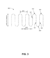
- FIG. 3 is a schematic illustration of a section of a serpentine wire according to certain embodiments.
- FIG. 4 depicts two interconnected solar cells according to certain embodiments.
- FIG. 5 depicts front and back views of a wire assembly according to certain embodiments.
- FIG. 6 depicts a cross-sectional view of a wire assembly according to certain embodiments.
- FIG. 7 depicts a cross-sectional view of a wire assembly according to certain embodiments.
- FIG. 8 is a plot depicting the efficiency of the solar cell versus the gauge of the wire in the wire assembly.
- FIG. 9 depicts a cross-sectional view of a wire assembly in which the third polymer film is too thick.
- FIG. 1 shows front ( 101 ) and back ( 103 ) views of a thin film solar cell, including a wire current collector/interconnect assembly.
- Front view 101 shows the front, or light facing, side of the solar cell including a conductive transparent top layer 107
- back view 103 shows a metallic substrate 111 supporting a thin film solar cell stack.
- FIG. 2 shows a perspective view of cell-width strips 200 of thin film solar cell stacks.
- Substrate 211 supports thin films 210 , 209 , 208 and 207 .
- Layers 208 and 209 form a p-n junction, with a p-type semiconductor layer 209 deposited on a back electrical contact layer 210 and a n-type semiconductor layer 208 deposited on p-type semiconductor layer 209 to complete a p-n junction.
- any suitable semiconductor material such as CIGS (copper indium gallium selenide), CIS (copper indium selenide), CdTe, CdS, ZnS, ZnO, amorphous silicon, polycrystalline silicon, etc. are used for layers 208 and 209 .
- the p-type semiconductor layer 209 is CIGS or CIS
- the n-type semiconductor layer 208 is CdS or a cadmium free material, such as ZnS, ZnO, etc.
- Top electrode layer 207 overlays the p-n junction. Top electrode layer 207 is transparent, allowing light to reach light absorbing layer 209 .
- top electrode layer 207 is a transparent conducting oxide (TCO), for example, zinc oxide, aluminum-doped zinc oxide (AZO), indium tin oxide (ITO), and gallium doped zinc oxide.
- TCO transparent conducting oxide
- Back electrical contact layer 210 provides electrical contact to allow electrical current to flow through the solar cell, and may be made of any appropriate material, e.g., molybdenum, niobium, copper, silver, etc.
- substrate 211 is a metallic substrate, e.g., a thin stainless steel foil, though it may also be other metals including, but not limited to, titanium, copper, aluminum, beryllium, and the like.
- the substrate 211 may be relatively thin, less than or equal to about 2 to 10 mils (a mil is a thousandth of an inch, i.e., 1/1000 inch) in some instances, though other suitable thicknesses may also be used. In many cases the substrate is thin enough to be flexible.
- the stacks 200 shown in FIG. 2 are long cell-width strips, which may be cut further to define individual cells as shown in FIG. 1 .
- the thin film solar cells stacks shown in FIG. 2 are provided for context and not intended to be limiting.
- the wire current collectors and/or interconnects described herein may be used with other types of solar cells as well as in other fields.
- the wire assembly includes serpentine wire 113 and wire carriers or decals 115 and 117 .
- wire 113 is in a serpentine pattern, though other patterns are within the scope of the invention.
- the wire is configured in a pattern that spans a length of a decal and traverses an edge of the decal along the length of the decal.
- wire 113 is configured as a current collector to collect current generated by the solar cell and as a solar cell interconnect to electrically connect the cell to another cell, for example, in a solar module.
- the wire may be configured only as a current collector or only as an interconnect.
- Wire 113 overlays conductive transparent top layer 107 , and collects current generated from the cell.
- Wire 113 is typically a thin, highly conductive metal wire. Examples of wire metals include copper, aluminum, nickel, chrome, or alloys thereof. In some embodiments, a nickel coated copper wire is used. The wire should be able to maintain the serpentine or other form without significant material strain. In certain embodiments, the wire is 24 to 56 gauge, or in particular embodiments, 32 to 56 gauge, for example 40 to 50 gauge. In specific embodiments, the wire has a gauge of 34, 36, 40, 42, 44, or 46.
- Front decal 115 overlays all or part of portion 119 .
- Front decal 115 is a transparent, insulating carrier for the conductive wire.
- decal materials include thermoplastic materials such as polyethylene terephthalate (PET), ionomer resins (e.g., poly(ethylene-co-methacrylic acid), commercially available as SurlynTM, E. I. du Pont de Nemours and Company), polyamide, polyetheretherketone (PEEK), or combinations of these.
- FIG. 3 shows a section 300 of a serpentine wire according to embodiments of the invention.
- the term “serpentine” refers to a form having substantially uniformly spaced, substantially co-extensive and substantially parallel lengths of wire connected via substantially rounded end portions. Uniformly spaced, co-extensive, parallel lengths 301 connected by rounded end portions 303 are indicated in FIG. 3 .
- the pitch of the serpentine wire determines the distance current travels through the transparent conducting oxide prior to reaching the highly conductive wire. As shown in FIG. 3 , the maximum distance current has to travel through the transparent conductive oxide is 1 ⁇ 4 pitch. Reducing the pitch increases current collection. It also decreases the useful surface area of the cell, however, by covering the light absorbing layer. In certain embodiments, the pitch is between about 4 and 10 mm, e.g., about 6.5 mm, though other distances may also be used, as appropriate.
- view 103 depicts metallic substrate 111 and interconnect portion 121 of serpentine wire 113 .
- Back decal 117 which overlies portion 121 of serpentine wire 113 as shown in view 103 , is an insulating carrier for serpentine wire 113 .
- the conductive side of interconnect portion 121 faces down, able to make contact with a metallic substrate of an adjacent cell.
- FIG. 4 shows the backsides of cells 410 a and 410 b including metallic substrates 411 a and 411 b .
- Wire interconnect 421 b of cell 410 b overlies metallic substrate 411 a of cell 410 a , thereby electrically connecting the cells 410 a and 410 b.
- the serpentine wire is provided on an insulating carrier, such as front and back decals described with reference to FIG. 1 .
- FIG. 5 depicts front and back views of a strip of a wire assembly including serpentine wire 513 and front and back decals 515 and 517 , respectively.
- Front view 501 shows serpentine wire 513 and front decal 515 , which overlies a portion of wire 513 .
- Back decal 517 is not depicted in view 501 for clarity.
- Exposed portion 521 of wire 513 interconnects the cell as depicted in FIG. 4 .
- Back view 503 shows serpentine wire 513 and back decal 517 , which overlies a portion of wire 513 .
- Exposed portion 519 of wire 513 faces the top conducting oxide and acts as a current collector.
- a wire assembly is affixed to the front side of a cell or cell width strip (such as those shown in FIG. 2 ).
- one or more of the decals do not overlie the rounded end portions of the serpentine wire.
- FIG. 6 depicts a cross-sectional view of a wire assembly along line 1 - 1 of FIG. 5 , according to certain embodiments.
- the wire assembly includes top decal 515 , bottom decal 517 , and serpentine wire 513 .
- Top decal 515 and bottom decal 517 include first polymer film 602 , second polymer film 604 , and third polymer film 606 .
- the first polymer film contacts the second polymer film and the second polymer film contacts the third polymer film.
- top decal 515 and bottom decal 517 include the same polymer film stacks, but in other embodiments, the top decal and the bottom decal have different polymer film stacks. Further, in some embodiments, one or both of the top decal and the bottom decal does not include first polymer 602 .
- top decal 515 and bottom decal 517 overlap. In different embodiments, the amount of this overlap is variable, and in some embodiments, top decal 515 and bottom decal 517 do not overlap.
- the dimensions of the top decal (i.e., the thicknesses and widths of the first polymer film, the second polymer film, and the third polymer film) and the bottom decal are the same in some embodiments, and different in other embodiments.
- FIG. 7 depicts a cross-sectional view of a wire assembly along line 2 - 2 of FIG. 5 , according to certain embodiments.
- FIG. 7 shows top decal 515 and serpentine wire 513 embedded in third polymer film 606 of the top decal.
- Top decal 515 also includes first polymer film 602 and second polymer film 604 .
- a surface of the wire facing away from second polymer film 604 is exposed.
- the exposed surface of the wire makes electrical contact with a layer of material underlying the third polymer film.
- the exposed surface of the wire makes electrical contact with a transparent conducting oxide layer.
- the polymer films are thermoplastic polymer films.
- the polymer films may be thermoplastic polymer films such as polyethylene terephthalate (PET) films, poly(methyl methacrylate) (PMMA) films, fluorinated ethylene propylene (FEP) films, ethylene tetrafluoroethylene (ETFE) films, polycarbonate films, polyamide films, polyetheretherketone films (PEEK) films, low density polyethylene films, low density urethane films, or low density polymer (with ionomer functionality) films (e.g., poly(ethylene-co-methacrylic acid) (SurlynTM)).
- PET polyethylene terephthalate
- PMMA poly(methyl methacrylate)
- FEP fluorinated ethylene propylene
- ETFE ethylene tetrafluoroethylene
- PEEK polyetheretherketone films
- low density polyethylene films low density urethane films
- low density polymer (with ionomer functionality) films e.
- the second polymer film is a polyethylene terephthalate (PET) film, a poly(methyl methacrylate) (PMMA) film, a fluorinated ethylene propylene (FEP) film, an ethylene tetrafluoroethylene (ETFE) film, or a polycarbonate film.
- PET polyethylene terephthalate
- PMMA poly(methyl methacrylate)
- FEP fluorinated ethylene propylene
- ETFE ethylene tetrafluoroethylene
- the first polymer film and the third polymer film are the same type of polymer film in some embodiments, and in other embodiments, they are different types of polymer film.
- the first and the third polymer films are a low density polyethylene film, a low density urethane film, or a low density polymer (with ionomer functionality) film.
- the first and the third polymer films are films of poly(ethylene-co-methacrylic acid) (SurlynTM).
- the first, second, and third polymer films are thermoplastic polymer films, with the melting point temperature of the second thermoplastic polymer film being greater than the melting point temperatures of the first and the third polymer films. This difference in melting point temperatures allows the serpentine wire to be heated in the fabrication process of a wire assembly and be embedded in the third polymer film but not the second polymer film.
- the third polymer film is a poly(ethylene-co-methacrylic acid) film and the second polymer film is a polyethylene terephthalate film.
- Polyethylene terephthalate has a melting point of greater than about 250° C.
- poly(ethylene-co-methacrylic acid) has a melting point of about 90° C.
- These melting point temperatures vary with the processing and manufacturing methods of the polymer films. This difference in melting point temperatures allow a wire heated to about 120° C., for example, to be embedded in the third polymer film but not the second polymer film.
- the second polymer film acts as a barrier through which the heated wire will not pass.
- the wire is in contact with the second polymer film, as depicted in FIG.
- the wire is not in contact with the second polymer film.
- the layer of adhesive is a layer of polyurethane adhesive.
- the thickness of the layer of adhesive is about 0.5 microns to 10 microns.
- the first polymer film and/or the third polymer film are an adhesive material.
- a non-polymeric adhesive material is used in place of the first polymer film and/or the third polymer film.
- the adhesive material is a silicone-based polymer.
- Some examples of such adhesive materials include the following materials available from Dow Corning in Midland, Mich.: two part translucent heat cure adhesive (part number SE1700), and two part fast cure low modulus adhesive (part numbers JCR6115 and JCR 6140).
- the adhesive material is a thermoset polymer material. Examples of such adhesive materials include polyurethanes, epoxies, silicones, acrylics and/or combinations of these materials.
- a further example of such an adhesive material is a reactively functionalized polyolefin (e.g., with functional acrylate groups).
- the adhesive material has pressure sensitive adhesive characteristics and may be cross-linked with ultra-violet light, an electron beam, or thermal energy.
- an advantage of an adhesive material that has pressure sensitive adhesive characteristics is that such an adhesive material does not rely on the thermal capacity of the wire in the fabrication process for a wire assembly; the adhesive material should have a sufficiently sticky formulation in these embodiments.
- a similar advantage is present for adhesive materials that are fast cure adhesives; the adhesive material should have a sufficiently fast cure time in these embodiments.
- thermoset polymer materials or materials that are cross-linked are more resistant to flow at higher temperatures than thermoplastic polymer materials. This resistance to flow at higher temperatures also improves the adhesion of the wire to the adhesive material.
- the efficiency (i.e., the power output) of the thin film solar cells incorporating the wire assemblies described above depends on a number of factors. With an increased area of the semiconductor materials not covered by the wire, the efficiency of a thin film solar cell increases. Thus, by increasing the gauge of the wire (with increasing wire gauge, the diameter of the wire decreases), the efficiency of the thin film solar cell increases. In some instances, an about 2 to 3% increase in efficiency has been observed by increasing the wire gauge. In other instances, an about 4 to 5% increase in efficiency has been observed. The effect of exposing more semiconductor material by increasing the wire gauge increases efficiency up to a certain point, however, and then efficiency decreases with increasing wire gauge, as shown in FIG. 8 .
- the third polymer film is thin enough such that the wire is not completely encased in the third polymer film.
- a third polymer film with a thickness of about 2 mils accomplishes this. With higher gauge wire, however, a thinner third polymer film may be used. If the third polymer film is too thick, the wire may not contact the second polymer film and the wire may “float” in the third polymer film; i.e., if the third polymer film is too thick, a surface of the wire facing away from the second polymer film may not be exposed and therefore be unable to make electrical contact with a layer underlying the third polymer film.
- FIG. 9 depicts a cross-sectional view of a wire assembly, similar to cross-sectional view of the wire assembly shown in FIG. 7 .
- the third polymer film is too thick.
- FIG. 9 shows decal 915 and serpentine wire 513 embedded in third polymer film 906 of the decal.
- Decal 915 also includes first polymer film 902 and second polymer film 904 . Due to third polymer film 906 being too thick, however, a surface of the wire facing away from second polymer film 904 is not exposed. Due to the wire not being exposed, the wire would be unable to make electrical contact with any material underlying the third polymer. This might render a thin film solar cell unusable, depending on the configuration.
- the wire may delaminate and become detached from the second polymer film.
- the thickness of the third polymer film is about 1 ⁇ 4 to 1 ⁇ 2 the diameter of the wire in order to accomplish the above-described requirements. Further, using a thinner third polymer film reduces material costs.
- the third polymer film when the wire is about 36 to 46 gauge, is about 0.5 to 1.5 mils thick. In a specific embodiment, the wire is about 40 gauge. In another specific embodiment in which the wire is about 40 gauge, the third polymer film is about 0.75 to 1.5 mils thick. In certain embodiments, the ratio of the thickness of the first polymer film, the second polymer film, and the third polymer film is between about 1:1:1 and 1:2:1.
- the wire is heated and contacted with a third polymer film that is part of a decal.
- the heated wire adheres to the thermoplastic.
- Further description of fabrication methods for wire assemblies is given in U.S. Provisional Patent Application No. 61/348,642, filed May 26, 2010, and entitled “APPARATUS AND METHOD FOR SECURING WIRE TO DECAL,” which is incorporated by reference in its entirety.
- to fabricate a wire assembly when the third polymer film is an adhesive material the wire is contacted with an adhesive material that is part of a decal. The wire adheres to the adhesive material.
- the adhesive material is thermoset polymer or a material that cross-links/cures
- the adhesive material is exposed to ultra-violet light, an electron beam, or a heat source to cross-link and/or cure the adhesive material.
- thermoplastics such as poly(ethylene-co-methacrylic acid) (SurlynTM) for the third film.
- a blown film extrusion process may be used. In a blown film extrusion process, a polymer is extruded through a die configured as an upright cylinder with a circular opening. As the polymer is extruded, compressed air may be forced into the center of the extruded cylindrical profile, created a bubble. The bubble is then collapsed onto itself to form a thin sheet of polymer. It is difficult, however, to reproducibly produce poly(ethylene-co-methacrylic acid) films thinner than about 2 mils using a blown film process.
- an extrusion coating process is used.
- an extrusion coating process an additional layer of one polymer is coated onto an existing film.
- poly(ethylene-co-methacrylic acid) is extruded through a die onto a polyethylene terephthalate film.
- the configuration of the die is used to control the thickness of the poly(ethylene-co-methacrylic acid) film.
- the two film structure may then be passed through cold rollers.
- Extrusion coating may be used to reproducibly produce poly(ethylene-co-methacrylic acid) films down to about 1 ⁇ 2 mil thickness.
- Another challenge is handling the high gauge wire itself.
- Higher gauge wire is thinner, and has a lower yield strength than thicker wire.
- the yield strength of 34 gauge wire used in some embodiments is about 4 times higher than the yield strength of 40 gauge wire used in other embodiments.
- the lower yield strength of the higher gauge wire presents challenges in forming it into a serpentine pattern.
- thinner wire has a lower thermal capacity than thicker wire.
- the lower thermal capacity presents challenges in embedding the wire in a thermoplastic polymer film due to the wire cooling off rapidly after it is heated.
- modifications to the fabrication process may be made.
- the fabrication process may be modified such that less stress is put on higher gauge wire so that it does not yield.
- higher gauge wire may be heated to higher temperatures (e.g., with additional or more powerful heating zones in the fabrication process) such that when the wire cools, it is still at a high enough temperature to be embedded in a thermoplastic polymer film.
Landscapes
- Life Sciences & Earth Sciences (AREA)
- Sustainable Development (AREA)
- Physics & Mathematics (AREA)
- Condensed Matter Physics & Semiconductors (AREA)
- Electromagnetism (AREA)
- General Physics & Mathematics (AREA)
- Engineering & Computer Science (AREA)
- Computer Hardware Design (AREA)
- Microelectronics & Electronic Packaging (AREA)
- Power Engineering (AREA)
- Photovoltaic Devices (AREA)
Abstract
Description
Claims (18)
Priority Applications (3)
| Application Number | Priority Date | Filing Date | Title |
|---|---|---|---|
| US12/897,162 US10026859B2 (en) | 2010-10-04 | 2010-10-04 | Small gauge wire solar cell interconnect |
| PCT/US2011/052974 WO2012047553A2 (en) | 2010-10-04 | 2011-09-23 | Small gauge wire solar cell interconnect |
| US15/971,955 US20180331244A1 (en) | 2010-10-04 | 2018-05-04 | Small gauge wire solar cell interconnect |
Applications Claiming Priority (1)
| Application Number | Priority Date | Filing Date | Title |
|---|---|---|---|
| US12/897,162 US10026859B2 (en) | 2010-10-04 | 2010-10-04 | Small gauge wire solar cell interconnect |
Related Child Applications (1)
| Application Number | Title | Priority Date | Filing Date |
|---|---|---|---|
| US15/971,955 Continuation US20180331244A1 (en) | 2010-10-04 | 2018-05-04 | Small gauge wire solar cell interconnect |
Publications (2)
| Publication Number | Publication Date |
|---|---|
| US20120080079A1 US20120080079A1 (en) | 2012-04-05 |
| US10026859B2 true US10026859B2 (en) | 2018-07-17 |
Family
ID=45888747
Family Applications (2)
| Application Number | Title | Priority Date | Filing Date |
|---|---|---|---|
| US12/897,162 Active 2033-05-31 US10026859B2 (en) | 2010-10-04 | 2010-10-04 | Small gauge wire solar cell interconnect |
| US15/971,955 Abandoned US20180331244A1 (en) | 2010-10-04 | 2018-05-04 | Small gauge wire solar cell interconnect |
Family Applications After (1)
| Application Number | Title | Priority Date | Filing Date |
|---|---|---|---|
| US15/971,955 Abandoned US20180331244A1 (en) | 2010-10-04 | 2018-05-04 | Small gauge wire solar cell interconnect |
Country Status (2)
| Country | Link |
|---|---|
| US (2) | US10026859B2 (en) |
| WO (1) | WO2012047553A2 (en) |
Families Citing this family (18)
| Publication number | Priority date | Publication date | Assignee | Title |
|---|---|---|---|---|
| US8664030B2 (en) | 1999-03-30 | 2014-03-04 | Daniel Luch | Collector grid and interconnect structures for photovoltaic arrays and modules |
| US20100108118A1 (en) * | 2008-06-02 | 2010-05-06 | Daniel Luch | Photovoltaic power farm structure and installation |
| US8822810B2 (en) | 2006-04-13 | 2014-09-02 | Daniel Luch | Collector grid and interconnect structures for photovoltaic arrays and modules |
| US9006563B2 (en) | 2006-04-13 | 2015-04-14 | Solannex, Inc. | Collector grid and interconnect structures for photovoltaic arrays and modules |
| US8729385B2 (en) | 2006-04-13 | 2014-05-20 | Daniel Luch | Collector grid and interconnect structures for photovoltaic arrays and modules |
| US9236512B2 (en) | 2006-04-13 | 2016-01-12 | Daniel Luch | Collector grid and interconnect structures for photovoltaic arrays and modules |
| US9865758B2 (en) | 2006-04-13 | 2018-01-09 | Daniel Luch | Collector grid and interconnect structures for photovoltaic arrays and modules |
| US8884155B2 (en) | 2006-04-13 | 2014-11-11 | Daniel Luch | Collector grid and interconnect structures for photovoltaic arrays and modules |
| US20110197947A1 (en) | 2008-03-20 | 2011-08-18 | Miasole | Wire network for interconnecting photovoltaic cells |
| US20100043863A1 (en) * | 2008-03-20 | 2010-02-25 | Miasole | Interconnect assembly |
| US8912429B2 (en) * | 2008-03-20 | 2014-12-16 | Hanergy Holding Group Ltd. | Interconnect assembly |
| US8356640B1 (en) | 2010-01-14 | 2013-01-22 | Mia Solé | Apparatuses and methods for fabricating wire current collectors and interconnects for solar cells |
| US9061344B1 (en) | 2010-05-26 | 2015-06-23 | Apollo Precision (Fujian) Limited | Apparatuses and methods for fabricating wire current collectors and interconnects for solar cells |
| US10026859B2 (en) | 2010-10-04 | 2018-07-17 | Beijing Apollo Ding Rong Solar Technology Co., Ltd. | Small gauge wire solar cell interconnect |
| US8951824B1 (en) | 2011-04-08 | 2015-02-10 | Apollo Precision (Fujian) Limited | Adhesives for attaching wire network to photovoltaic cells |
| DE102014107454B4 (en) | 2014-05-27 | 2016-05-19 | Xenon Automatisierungstechnik Gmbh | Device for producing a busbar for contacting solar cells |
| US9559233B2 (en) | 2014-09-25 | 2017-01-31 | Sunpower Corporation | Solar cell interconnection |
| JP7272073B2 (en) * | 2019-04-08 | 2023-05-12 | 大日本印刷株式会社 | COLLECTOR WIRE FIXING FILM FOR SOLAR CELL MODULE AND SOLAR CELL MODULE USING THE SAME |
Citations (119)
| Publication number | Priority date | Publication date | Assignee | Title |
|---|---|---|---|---|
| US2782809A (en) | 1954-01-25 | 1957-02-26 | Genesee Machine Builders Inc | Coil winding machine |
| US2963048A (en) | 1954-05-24 | 1960-12-06 | W F And John Barnes Company | Apparatus for bending wire articles |
| US3025889A (en) | 1960-02-04 | 1962-03-20 | Baird Machine Co | Wire forming machines |
| US3376164A (en) | 1963-08-01 | 1968-04-02 | Globe Union Inc | Photovoltaic power assembly |
| US3459391A (en) | 1964-02-13 | 1969-08-05 | Nasa | Interconnection of solar cells |
| US3553030A (en) | 1967-11-15 | 1971-01-05 | Philips Corp | Radiation-sensitive semiconductor device |
| US3561500A (en) | 1968-09-30 | 1971-02-09 | Gen Electric | Wire-forming apparatus and method |
| US3713893A (en) | 1969-11-20 | 1973-01-30 | Gould Inc | Integrated solar cell array |
| US4017332A (en) | 1975-02-27 | 1977-04-12 | Varian Associates | Solar cells employing stacked opposite conductivity layers |
| US4019924A (en) | 1975-11-14 | 1977-04-26 | Mobil Tyco Solar Energy Corporation | Solar cell mounting and interconnecting assembly |
| DE2757301A1 (en) | 1977-12-22 | 1979-07-05 | Leybold Heraeus Gmbh & Co Kg | Multiple element solar cell - has semiconductor elements enclosed between conductive and insulating layers with ends folded over and interlocked |
| US4166918A (en) | 1978-07-19 | 1979-09-04 | Rca Corporation | Method of removing the effects of electrical shorts and shunts created during the fabrication process of a solar cell |
| DE2919041A1 (en) | 1979-05-11 | 1980-11-13 | Messerschmitt Boelkow Blohm | SOLAR CELL ARRANGEMENT |
| US4346159A (en) | 1977-02-14 | 1982-08-24 | Fuji Xerox Co., Ltd. | Photosensitive element for electrophotography |
| US4366335A (en) | 1981-01-05 | 1982-12-28 | Exxon Research And Engineering Co. | Indium oxide/n-silicon heterojunction solar cells |
| US4499658A (en) * | 1983-09-06 | 1985-02-19 | Atlantic Richfield Company | Solar cell laminates |
| JPS60128647A (en) | 1983-12-16 | 1985-07-09 | Hitachi Ltd | Flexible film conductor lead and solar battery utilizing the same |
| US4560498A (en) | 1975-08-04 | 1985-12-24 | Raychem Corporation | Positive temperature coefficient of resistance compositions |
| US4567642A (en) | 1984-09-28 | 1986-02-04 | The Standard Oil Company | Method of making photovoltaic modules |
| US4574160A (en) | 1984-09-28 | 1986-03-04 | The Standard Oil Company | Flexible, rollable photovoltaic cell module |
| US4598306A (en) | 1983-07-28 | 1986-07-01 | Energy Conversion Devices, Inc. | Barrier layer for photovoltaic devices |
| US4640002A (en) | 1982-02-25 | 1987-02-03 | The University Of Delaware | Method and apparatus for increasing the durability and yield of thin film photovoltaic devices |
| US4652693A (en) | 1985-08-30 | 1987-03-24 | The Standard Oil Company | Reformed front contact current collector grid and cell interconnect for a photovoltaic cell module |
| US4694117A (en) | 1985-05-04 | 1987-09-15 | Telefunken Electronic Gmbh | Solar cell |
| US4849133A (en) | 1986-10-24 | 1989-07-18 | Nippon Mektron, Ltd. | PTC compositions |
| US5034068A (en) | 1990-02-23 | 1991-07-23 | Spectrolab, Inc. | Photovoltaic cell having structurally supporting open conductive back electrode structure, and method of fabricating the cell |
| EP0440869A1 (en) | 1990-02-09 | 1991-08-14 | Bio-Photonics, Inc. | Photovoltaic element able to convert solar radiation into electric current and photoelectric battery |
| JPH0621501A (en) | 1992-03-31 | 1994-01-28 | Canon Inc | Solar cell module and manufacture thereof |
| US5330583A (en) | 1991-09-30 | 1994-07-19 | Sharp Kabushiki Kaisha | Solar battery module |
| US5391235A (en) | 1992-03-31 | 1995-02-21 | Canon Kabushiki Kaisha | Solar cell module and method of manufacturing the same |
| JPH0799334A (en) | 1993-08-06 | 1995-04-11 | Canon Inc | Photovoltaic element and module |
| US5474621A (en) | 1994-09-19 | 1995-12-12 | Energy Conversion Devices, Inc. | Current collection system for photovoltaic cells |
| US5554229A (en) | 1995-02-21 | 1996-09-10 | United Solar Systems Corporation | Light directing element for photovoltaic device and method of manufacture |
| JPH0936404A (en) | 1995-07-17 | 1997-02-07 | Canon Inc | Current collection electrode, photovolataic power element and production thereof |
| US5620528A (en) | 1994-09-30 | 1997-04-15 | Siemens Solar Gmbh | Solar cell with a connecting structure |
| US5626688A (en) | 1994-12-01 | 1997-05-06 | Siemens Aktiengesellschaft | Solar cell with chalcopyrite absorber layer |
| US5681402A (en) | 1994-11-04 | 1997-10-28 | Canon Kabushiki Kaisha | Photovoltaic element |
| JPH1093125A (en) | 1996-09-13 | 1998-04-10 | Sanyo Electric Co Ltd | Solar cell module |
| US5759291A (en) | 1995-06-28 | 1998-06-02 | Canon Kabushiki Kaisha | Photovoltaic cell and method of making the same |
| US5814195A (en) | 1995-04-25 | 1998-09-29 | The Boc Group, Inc. | Sputtering system using cylindrical rotating magnetron electrically powered using alternating current |
| KR19990006965A (en) | 1997-06-13 | 1999-01-25 | 미따라이 후지오 | Solar cell module, production method thereof, and installation method of solar cell modules |
| EP0949686A1 (en) | 1998-04-08 | 1999-10-13 | Coöperatief Advies en Onderzoeksburo u.a. Ecofys | Device for supporting a solar panel on a slanting roof |
| CA2335159A1 (en) | 1998-06-16 | 1999-12-23 | Wilco Johan Thomas Plantfeber | Roofing element comprising at least one solar cell |
| US6093884A (en) | 1997-11-06 | 2000-07-25 | Canon Kabushiki Kaisha | Solar cell module, solar cell array having the module, power generation apparatus using the array, and inspection method and construction method of the apparatus |
| US6114046A (en) | 1997-07-24 | 2000-09-05 | Evergreen Solar, Inc. | Encapsulant material for solar cell module and laminated glass applications |
| US6121542A (en) | 1996-05-17 | 2000-09-19 | Canon Kabushiki Kaisha | Photovoltaic device |
| JP2000269531A (en) | 1999-01-14 | 2000-09-29 | Canon Inc | Solar battery module, building material therewith envelope thereof and photovoltaic power generation device |
| US6132585A (en) | 1992-07-01 | 2000-10-17 | Canon Kabushiki Kaisha | Semiconductor element and method and apparatus for fabricating the same |
| US6184457B1 (en) | 1997-12-22 | 2001-02-06 | Canon Kabushiki Kaisha | Photovoltaic device module |
| US6184458B1 (en) | 1998-06-11 | 2001-02-06 | Canon Kabushiki Kaisha | Photovoltaic element and production method therefor |
| US6231732B1 (en) | 1997-08-26 | 2001-05-15 | Scivac | Cylindrical carriage sputtering system |
| US6335479B1 (en) | 1998-10-13 | 2002-01-01 | Dai Nippon Printing Co., Ltd. | Protective sheet for solar battery module, method of fabricating the same and solar battery module |
| US20020014262A1 (en) | 2000-07-10 | 2002-02-07 | Masaaki Matsushita | Photovoltaic power generation systems and methods of controlling photovoltaic power generation systems |
| US6365010B1 (en) | 1998-11-06 | 2002-04-02 | Scivac | Sputtering apparatus and process for high rate coatings |
| US6372538B1 (en) | 2000-03-16 | 2002-04-16 | University Of Delaware | Fabrication of thin-film, flexible photovoltaic module |
| US20020166580A1 (en) | 2001-03-20 | 2002-11-14 | The Boeing Company | Method for fabricating a solar tile |
| US6488824B1 (en) | 1998-11-06 | 2002-12-03 | Raycom Technologies, Inc. | Sputtering apparatus and process for high rate coatings |
| US6531653B1 (en) | 2001-09-11 | 2003-03-11 | The Boeing Company | Low cost high solar flux photovoltaic concentrator receiver |
| US6548912B1 (en) | 1999-10-25 | 2003-04-15 | Battelle Memorial Institute | Semicoductor passivation using barrier coatings |
| US6600100B2 (en) | 1998-05-28 | 2003-07-29 | Emcore Corporation | Solar cell having an integral monolithically grown bypass diode |
| US6657119B2 (en) | 1999-01-15 | 2003-12-02 | Forskarpatent I Uppsala Ab | Electric connection of electrochemical and photoelectrochemical cells |
| US20040063320A1 (en) | 2002-09-30 | 2004-04-01 | Hollars Dennis R. | Manufacturing apparatus and method for large-scale production of thin-film solar cells |
| US20040069340A1 (en) | 1999-03-30 | 2004-04-15 | Daniel Luch | Substrate and collector grid structures for integrated series connected photovoltaic arrays and process of manufacture of such arrays |
| US6743524B2 (en) | 2002-05-23 | 2004-06-01 | General Electric Company | Barrier layer for an article and method of making said barrier layer by expanding thermal plasma |
| US20040118448A1 (en) | 2002-09-05 | 2004-06-24 | Nanosys, Inc. | Nanostructure and nanocomposite based compositions and photovoltaic devices |
| US20040144043A1 (en) | 2003-01-23 | 2004-07-29 | Stevenson Edward J | Integrated photovoltaic roofing component and panel |
| JP2004253475A (en) | 2003-02-18 | 2004-09-09 | Sharp Corp | Solar cell module, its producing process and heat source for use therein |
| US20040187917A1 (en) | 2003-03-29 | 2004-09-30 | Nanosolar, Inc. | Transparent electrode, optoelectronic apparatus and devices |
| US6803513B2 (en) | 2002-08-20 | 2004-10-12 | United Solar Systems Corporation | Series connected photovoltaic module and method for its manufacture |
| US20050072461A1 (en) | 2003-05-27 | 2005-04-07 | Frank Kuchinski | Pinhole porosity free insulating films on flexible metallic substrates for thin film applications |
| US20050074915A1 (en) | 2001-07-13 | 2005-04-07 | Tuttle John R. | Thin-film solar cell fabricated on a flexible metallic substrate |
| JP2005129773A (en) | 2003-10-24 | 2005-05-19 | Kyocera Corp | Solar cell module and wiring for connecting solar cell element |
| US20050176270A1 (en) | 2004-02-11 | 2005-08-11 | Daniel Luch | Methods and structures for the production of electrically treated items and electrical connections |
| DE10393252T5 (en) | 2002-09-06 | 2005-09-08 | Dai Nippon Printing Co., Ltd. | Backside protective layer for a solar cell module and solar cell module using the same |
| US20050241692A1 (en) * | 2002-08-29 | 2005-11-03 | Rubin Leonid B | Electrode for photovoltaic cells, photovoltaic cell and photovoltaic module |
| US20050274408A1 (en) | 2004-06-01 | 2005-12-15 | Lian Li | Photovoltaic module architecture |
| JP2006041351A (en) | 2004-07-29 | 2006-02-09 | Canon Inc | Process for manufacturing photovoltaic element |
| US20060180195A1 (en) | 1999-03-30 | 2006-08-17 | Daniel Luch | Substrate and collector grid structures for integrated photovoltaic arrays and process of manufacture of such arrays |
| US20060207646A1 (en) | 2003-07-07 | 2006-09-21 | Christine Terreau | Encapsulation of solar cells |
| WO2007116806A1 (en) | 2006-03-31 | 2007-10-18 | Pioneer Corporation | Low resistance substrate manufacturing method |
| US20070283997A1 (en) | 2006-06-13 | 2007-12-13 | Miasole | Photovoltaic module with integrated current collection and interconnection |
| US20070283996A1 (en) | 2006-06-13 | 2007-12-13 | Miasole | Photovoltaic module with insulating interconnect carrier |
| EP1868250A2 (en) | 2006-06-13 | 2007-12-19 | Miasole | Photovoltaic module with integrated current collection and interconnection |
| US20070295390A1 (en) * | 2006-05-05 | 2007-12-27 | Nanosolar, Inc. | Individually encapsulated solar cells and solar cell strings having a substantially inorganic protective layer |
| US20070295385A1 (en) | 2006-05-05 | 2007-12-27 | Nanosolar, Inc. | Individually encapsulated solar cells and solar cell strings having a substantially inorganic protective layer |
| US20080000518A1 (en) | 2006-03-28 | 2008-01-03 | Basol Bulent M | Technique for Manufacturing Photovoltaic Modules |
| US20080011350A1 (en) | 1999-03-30 | 2008-01-17 | Daniel Luch | Collector grid, electrode structures and interconnect structures for photovoltaic arrays and other optoelectric devices |
| US20080053511A1 (en) | 2004-04-28 | 2008-03-06 | Moritaka Nakamura | Integrated Wiring Member for Solar Cell Module, Solar Cell Module Using the Same, and Manufacturing Methods Thereof |
| US20080053519A1 (en) | 2006-08-30 | 2008-03-06 | Miasole | Laminated photovoltaic cell |
| US20080128018A1 (en) | 2006-12-04 | 2008-06-05 | Richard Allen Hayes | Solar cells which include the use of certain poly(vinyl butyral)/film bilayer encapsulant layers with a low blocking tendency and a simplified process to produce thereof |
| US20080142071A1 (en) | 2006-12-15 | 2008-06-19 | Miasole | Protovoltaic module utilizing a flex circuit for reconfiguration |
| US20080213477A1 (en) | 2007-03-02 | 2008-09-04 | Arno Zindel | Inline vacuum processing apparatus and method for processing substrates therein |
| US20080314432A1 (en) | 2007-06-19 | 2008-12-25 | Miasole | Photovoltaic module utilizing an integrated flex circuit and incorporating a bypass diode |
| US20080314433A1 (en) | 1995-05-15 | 2008-12-25 | Daniel Luch | Substrate structures for integrated series connected photovoltaic arrays and process of manufacture of such arrays |
| US20090014049A1 (en) | 2007-07-13 | 2009-01-15 | Miasole | Photovoltaic module with integrated energy storage |
| US20090014057A1 (en) | 2007-07-13 | 2009-01-15 | Miasole | Photovoltaic modules with integrated devices |
| US20090014058A1 (en) | 2007-07-13 | 2009-01-15 | Miasole | Rooftop photovoltaic systems |
| US20090111206A1 (en) | 1999-03-30 | 2009-04-30 | Daniel Luch | Collector grid, electrode structures and interrconnect structures for photovoltaic arrays and methods of manufacture |
| US20090199894A1 (en) | 2007-12-14 | 2009-08-13 | Miasole | Photovoltaic devices protected from environment |
| US20090235979A1 (en) * | 2008-03-20 | 2009-09-24 | Mulugeta Zerfu Wudu | Interconnect assembly |
| US20090297803A1 (en) | 2008-05-28 | 2009-12-03 | Kriha James A | Conductive Ink Formulations |
| US20100043863A1 (en) | 2008-03-20 | 2010-02-25 | Miasole | Interconnect assembly |
| US20100108122A1 (en) | 2008-11-04 | 2010-05-06 | Shawn Everson | Combined diode, lead assembly incorporating an expansion joint |
| WO2010056803A2 (en) | 2008-11-17 | 2010-05-20 | Miasole | Power-loss-inhibiting current-collector |
| US20100130348A1 (en) | 2007-09-21 | 2010-05-27 | Chul-Hyun Kang | Photocatalytic composition for anti-reflection and the glass substrate coated with the composition |
| US20100212733A1 (en) | 2009-02-20 | 2010-08-26 | Miasole | Protective layer for large-scale production of thin-film solar cells |
| US20110143077A1 (en) | 2008-07-04 | 2011-06-16 | Yasuo Kakihara | Process for producing transparent conductive transfer plate, transparent conductive transfer plate, process for producing transparent conductive substrate using the transparent conductive transfer plate, transparent conductive substrate, and molded product using the transparent conductive substrate |
| US20110197947A1 (en) | 2008-03-20 | 2011-08-18 | Miasole | Wire network for interconnecting photovoltaic cells |
| US20110207328A1 (en) | 2006-10-20 | 2011-08-25 | Stuart Philip Speakman | Methods and apparatus for the manufacture of microstructures |
| US20120000510A1 (en) | 2009-12-28 | 2012-01-05 | Global Solar Energy, Inc. | Laminated solar cell interconnection system |
| US8138413B2 (en) * | 2006-04-13 | 2012-03-20 | Daniel Luch | Collector grid and interconnect structures for photovoltaic arrays and modules |
| US20120080079A1 (en) | 2010-10-04 | 2012-04-05 | Miasole | Small gauge wire solar cell interconnect |
| US20120125393A1 (en) | 2010-11-22 | 2012-05-24 | Miasole | Photovoltaic Device and Method and System for Making Photovoltaic Device |
| US20120138117A1 (en) | 2008-03-20 | 2012-06-07 | Miasole | Thermoplastic wire network support for photovoltaic cells |
| US8356324B2 (en) | 2007-09-21 | 2013-01-15 | Broadcom Corporation | Implementing network personal video recorder for digital video settop boxes |
| US8356640B1 (en) | 2010-01-14 | 2013-01-22 | Mia Solé | Apparatuses and methods for fabricating wire current collectors and interconnects for solar cells |
| US8951824B1 (en) | 2011-04-08 | 2015-02-10 | Apollo Precision (Fujian) Limited | Adhesives for attaching wire network to photovoltaic cells |
| US20150136119A1 (en) | 2012-05-14 | 2015-05-21 | Helioclim | Method for shaping a film of a material that has low resistance to traction, and mirror comprising such a film |
| US9061344B1 (en) | 2010-05-26 | 2015-06-23 | Apollo Precision (Fujian) Limited | Apparatuses and methods for fabricating wire current collectors and interconnects for solar cells |
-
2010
- 2010-10-04 US US12/897,162 patent/US10026859B2/en active Active
-
2011
- 2011-09-23 WO PCT/US2011/052974 patent/WO2012047553A2/en active Application Filing
-
2018
- 2018-05-04 US US15/971,955 patent/US20180331244A1/en not_active Abandoned
Patent Citations (141)
| Publication number | Priority date | Publication date | Assignee | Title |
|---|---|---|---|---|
| US2782809A (en) | 1954-01-25 | 1957-02-26 | Genesee Machine Builders Inc | Coil winding machine |
| US2963048A (en) | 1954-05-24 | 1960-12-06 | W F And John Barnes Company | Apparatus for bending wire articles |
| US3025889A (en) | 1960-02-04 | 1962-03-20 | Baird Machine Co | Wire forming machines |
| US3376164A (en) | 1963-08-01 | 1968-04-02 | Globe Union Inc | Photovoltaic power assembly |
| US3459391A (en) | 1964-02-13 | 1969-08-05 | Nasa | Interconnection of solar cells |
| US3553030A (en) | 1967-11-15 | 1971-01-05 | Philips Corp | Radiation-sensitive semiconductor device |
| US3561500A (en) | 1968-09-30 | 1971-02-09 | Gen Electric | Wire-forming apparatus and method |
| US3713893A (en) | 1969-11-20 | 1973-01-30 | Gould Inc | Integrated solar cell array |
| US4017332A (en) | 1975-02-27 | 1977-04-12 | Varian Associates | Solar cells employing stacked opposite conductivity layers |
| US4560498A (en) | 1975-08-04 | 1985-12-24 | Raychem Corporation | Positive temperature coefficient of resistance compositions |
| US4019924A (en) | 1975-11-14 | 1977-04-26 | Mobil Tyco Solar Energy Corporation | Solar cell mounting and interconnecting assembly |
| US4346159A (en) | 1977-02-14 | 1982-08-24 | Fuji Xerox Co., Ltd. | Photosensitive element for electrophotography |
| DE2757301A1 (en) | 1977-12-22 | 1979-07-05 | Leybold Heraeus Gmbh & Co Kg | Multiple element solar cell - has semiconductor elements enclosed between conductive and insulating layers with ends folded over and interlocked |
| US4166918A (en) | 1978-07-19 | 1979-09-04 | Rca Corporation | Method of removing the effects of electrical shorts and shunts created during the fabrication process of a solar cell |
| DE2919041A1 (en) | 1979-05-11 | 1980-11-13 | Messerschmitt Boelkow Blohm | SOLAR CELL ARRANGEMENT |
| US4367581A (en) | 1979-05-11 | 1983-01-11 | Messerschmitt-Bolkow-Blohm Gmbh | Method of manufacturing an array of solar cells |
| US4366335A (en) | 1981-01-05 | 1982-12-28 | Exxon Research And Engineering Co. | Indium oxide/n-silicon heterojunction solar cells |
| US4640002A (en) | 1982-02-25 | 1987-02-03 | The University Of Delaware | Method and apparatus for increasing the durability and yield of thin film photovoltaic devices |
| US4598306A (en) | 1983-07-28 | 1986-07-01 | Energy Conversion Devices, Inc. | Barrier layer for photovoltaic devices |
| US4499658A (en) * | 1983-09-06 | 1985-02-19 | Atlantic Richfield Company | Solar cell laminates |
| JPS60128647A (en) | 1983-12-16 | 1985-07-09 | Hitachi Ltd | Flexible film conductor lead and solar battery utilizing the same |
| US4574160A (en) | 1984-09-28 | 1986-03-04 | The Standard Oil Company | Flexible, rollable photovoltaic cell module |
| US4567642A (en) | 1984-09-28 | 1986-02-04 | The Standard Oil Company | Method of making photovoltaic modules |
| US4694117A (en) | 1985-05-04 | 1987-09-15 | Telefunken Electronic Gmbh | Solar cell |
| US4652693A (en) | 1985-08-30 | 1987-03-24 | The Standard Oil Company | Reformed front contact current collector grid and cell interconnect for a photovoltaic cell module |
| US4849133A (en) | 1986-10-24 | 1989-07-18 | Nippon Mektron, Ltd. | PTC compositions |
| EP0440869A1 (en) | 1990-02-09 | 1991-08-14 | Bio-Photonics, Inc. | Photovoltaic element able to convert solar radiation into electric current and photoelectric battery |
| US5158618A (en) | 1990-02-09 | 1992-10-27 | Biophotonics, Inc. | Photovoltaic cells for converting light energy to electric energy and photoelectric battery |
| US5034068A (en) | 1990-02-23 | 1991-07-23 | Spectrolab, Inc. | Photovoltaic cell having structurally supporting open conductive back electrode structure, and method of fabricating the cell |
| US5330583A (en) | 1991-09-30 | 1994-07-19 | Sharp Kabushiki Kaisha | Solar battery module |
| US5391235A (en) | 1992-03-31 | 1995-02-21 | Canon Kabushiki Kaisha | Solar cell module and method of manufacturing the same |
| JPH0621501A (en) | 1992-03-31 | 1994-01-28 | Canon Inc | Solar cell module and manufacture thereof |
| US6132585A (en) | 1992-07-01 | 2000-10-17 | Canon Kabushiki Kaisha | Semiconductor element and method and apparatus for fabricating the same |
| JPH0799334A (en) | 1993-08-06 | 1995-04-11 | Canon Inc | Photovoltaic element and module |
| US5474621A (en) | 1994-09-19 | 1995-12-12 | Energy Conversion Devices, Inc. | Current collection system for photovoltaic cells |
| US5620528A (en) | 1994-09-30 | 1997-04-15 | Siemens Solar Gmbh | Solar cell with a connecting structure |
| US5681402A (en) | 1994-11-04 | 1997-10-28 | Canon Kabushiki Kaisha | Photovoltaic element |
| US5861324A (en) | 1994-11-04 | 1999-01-19 | Canon Kabushiki Kaisha | Method for producing photovoltaic element |
| US5626688A (en) | 1994-12-01 | 1997-05-06 | Siemens Aktiengesellschaft | Solar cell with chalcopyrite absorber layer |
| US5554229A (en) | 1995-02-21 | 1996-09-10 | United Solar Systems Corporation | Light directing element for photovoltaic device and method of manufacture |
| US5814195A (en) | 1995-04-25 | 1998-09-29 | The Boc Group, Inc. | Sputtering system using cylindrical rotating magnetron electrically powered using alternating current |
| US20080314433A1 (en) | 1995-05-15 | 2008-12-25 | Daniel Luch | Substrate structures for integrated series connected photovoltaic arrays and process of manufacture of such arrays |
| US5759291A (en) | 1995-06-28 | 1998-06-02 | Canon Kabushiki Kaisha | Photovoltaic cell and method of making the same |
| KR100242852B1 (en) | 1995-06-28 | 2000-02-01 | 미다라이 후지오 | Photovoltaic cell and method of making the same |
| JPH0936404A (en) | 1995-07-17 | 1997-02-07 | Canon Inc | Current collection electrode, photovolataic power element and production thereof |
| US6121542A (en) | 1996-05-17 | 2000-09-19 | Canon Kabushiki Kaisha | Photovoltaic device |
| JPH1093125A (en) | 1996-09-13 | 1998-04-10 | Sanyo Electric Co Ltd | Solar cell module |
| US6232544B1 (en) | 1997-06-13 | 2001-05-15 | Canon Kabushiki Kaisha | Solar cell module, production method thereof, and installation method of solar cell modules |
| US6093581A (en) | 1997-06-13 | 2000-07-25 | Canon Kabushiki Kaisha | Solar cell module, production method thereof, and installation method of solar cell modules |
| KR19990006965A (en) | 1997-06-13 | 1999-01-25 | 미따라이 후지오 | Solar cell module, production method thereof, and installation method of solar cell modules |
| US6114046A (en) | 1997-07-24 | 2000-09-05 | Evergreen Solar, Inc. | Encapsulant material for solar cell module and laminated glass applications |
| US6231732B1 (en) | 1997-08-26 | 2001-05-15 | Scivac | Cylindrical carriage sputtering system |
| US6093884A (en) | 1997-11-06 | 2000-07-25 | Canon Kabushiki Kaisha | Solar cell module, solar cell array having the module, power generation apparatus using the array, and inspection method and construction method of the apparatus |
| US6184457B1 (en) | 1997-12-22 | 2001-02-06 | Canon Kabushiki Kaisha | Photovoltaic device module |
| US6479744B1 (en) | 1997-12-22 | 2002-11-12 | Canon Kabushiki Kaisha | Photovoltaic device module |
| EP0949686A1 (en) | 1998-04-08 | 1999-10-13 | Coöperatief Advies en Onderzoeksburo u.a. Ecofys | Device for supporting a solar panel on a slanting roof |
| US6600100B2 (en) | 1998-05-28 | 2003-07-29 | Emcore Corporation | Solar cell having an integral monolithically grown bypass diode |
| US6184458B1 (en) | 1998-06-11 | 2001-02-06 | Canon Kabushiki Kaisha | Photovoltaic element and production method therefor |
| CA2335159A1 (en) | 1998-06-16 | 1999-12-23 | Wilco Johan Thomas Plantfeber | Roofing element comprising at least one solar cell |
| US6335479B1 (en) | 1998-10-13 | 2002-01-01 | Dai Nippon Printing Co., Ltd. | Protective sheet for solar battery module, method of fabricating the same and solar battery module |
| US6365010B1 (en) | 1998-11-06 | 2002-04-02 | Scivac | Sputtering apparatus and process for high rate coatings |
| US6488824B1 (en) | 1998-11-06 | 2002-12-03 | Raycom Technologies, Inc. | Sputtering apparatus and process for high rate coatings |
| JP2000269531A (en) | 1999-01-14 | 2000-09-29 | Canon Inc | Solar battery module, building material therewith envelope thereof and photovoltaic power generation device |
| US6657119B2 (en) | 1999-01-15 | 2003-12-02 | Forskarpatent I Uppsala Ab | Electric connection of electrochemical and photoelectrochemical cells |
| US20090111206A1 (en) | 1999-03-30 | 2009-04-30 | Daniel Luch | Collector grid, electrode structures and interrconnect structures for photovoltaic arrays and methods of manufacture |
| US20040069340A1 (en) | 1999-03-30 | 2004-04-15 | Daniel Luch | Substrate and collector grid structures for integrated series connected photovoltaic arrays and process of manufacture of such arrays |
| US20080011350A1 (en) | 1999-03-30 | 2008-01-17 | Daniel Luch | Collector grid, electrode structures and interconnect structures for photovoltaic arrays and other optoelectric devices |
| US20060180195A1 (en) | 1999-03-30 | 2006-08-17 | Daniel Luch | Substrate and collector grid structures for integrated photovoltaic arrays and process of manufacture of such arrays |
| US6548912B1 (en) | 1999-10-25 | 2003-04-15 | Battelle Memorial Institute | Semicoductor passivation using barrier coatings |
| US6372538B1 (en) | 2000-03-16 | 2002-04-16 | University Of Delaware | Fabrication of thin-film, flexible photovoltaic module |
| US20020014262A1 (en) | 2000-07-10 | 2002-02-07 | Masaaki Matsushita | Photovoltaic power generation systems and methods of controlling photovoltaic power generation systems |
| US20020166580A1 (en) | 2001-03-20 | 2002-11-14 | The Boeing Company | Method for fabricating a solar tile |
| US20050074915A1 (en) | 2001-07-13 | 2005-04-07 | Tuttle John R. | Thin-film solar cell fabricated on a flexible metallic substrate |
| US6531653B1 (en) | 2001-09-11 | 2003-03-11 | The Boeing Company | Low cost high solar flux photovoltaic concentrator receiver |
| US6743524B2 (en) | 2002-05-23 | 2004-06-01 | General Electric Company | Barrier layer for an article and method of making said barrier layer by expanding thermal plasma |
| US6803513B2 (en) | 2002-08-20 | 2004-10-12 | United Solar Systems Corporation | Series connected photovoltaic module and method for its manufacture |
| US20050241692A1 (en) * | 2002-08-29 | 2005-11-03 | Rubin Leonid B | Electrode for photovoltaic cells, photovoltaic cell and photovoltaic module |
| US20040118448A1 (en) | 2002-09-05 | 2004-06-24 | Nanosys, Inc. | Nanostructure and nanocomposite based compositions and photovoltaic devices |
| DE10393252T5 (en) | 2002-09-06 | 2005-09-08 | Dai Nippon Printing Co., Ltd. | Backside protective layer for a solar cell module and solar cell module using the same |
| US20040063320A1 (en) | 2002-09-30 | 2004-04-01 | Hollars Dennis R. | Manufacturing apparatus and method for large-scale production of thin-film solar cells |
| US7544884B2 (en) | 2002-09-30 | 2009-06-09 | Miasole | Manufacturing method for large-scale production of thin-film solar cells |
| US20050109392A1 (en) | 2002-09-30 | 2005-05-26 | Hollars Dennis R. | Manufacturing apparatus and method for large-scale production of thin-film solar cells |
| US6974976B2 (en) | 2002-09-30 | 2005-12-13 | Miasole | Thin-film solar cells |
| US20040144043A1 (en) | 2003-01-23 | 2004-07-29 | Stevenson Edward J | Integrated photovoltaic roofing component and panel |
| JP2004253475A (en) | 2003-02-18 | 2004-09-09 | Sharp Corp | Solar cell module, its producing process and heat source for use therein |
| US20040187917A1 (en) | 2003-03-29 | 2004-09-30 | Nanosolar, Inc. | Transparent electrode, optoelectronic apparatus and devices |
| US20050072461A1 (en) | 2003-05-27 | 2005-04-07 | Frank Kuchinski | Pinhole porosity free insulating films on flexible metallic substrates for thin film applications |
| US20060207646A1 (en) | 2003-07-07 | 2006-09-21 | Christine Terreau | Encapsulation of solar cells |
| JP2005129773A (en) | 2003-10-24 | 2005-05-19 | Kyocera Corp | Solar cell module and wiring for connecting solar cell element |
| US20050176270A1 (en) | 2004-02-11 | 2005-08-11 | Daniel Luch | Methods and structures for the production of electrically treated items and electrical connections |
| US20060032752A1 (en) | 2004-02-11 | 2006-02-16 | Daniel Luch | Methods and structures for the production of electrically treated items and electrical connections |
| US20080053511A1 (en) | 2004-04-28 | 2008-03-06 | Moritaka Nakamura | Integrated Wiring Member for Solar Cell Module, Solar Cell Module Using the Same, and Manufacturing Methods Thereof |
| US20050274408A1 (en) | 2004-06-01 | 2005-12-15 | Lian Li | Photovoltaic module architecture |
| JP2006041351A (en) | 2004-07-29 | 2006-02-09 | Canon Inc | Process for manufacturing photovoltaic element |
| US20080000518A1 (en) | 2006-03-28 | 2008-01-03 | Basol Bulent M | Technique for Manufacturing Photovoltaic Modules |
| US8142601B2 (en) | 2006-03-31 | 2012-03-27 | Pioneer Corporation | Method for manufacturing low resistance substrate |
| WO2007116806A1 (en) | 2006-03-31 | 2007-10-18 | Pioneer Corporation | Low resistance substrate manufacturing method |
| US8138413B2 (en) * | 2006-04-13 | 2012-03-20 | Daniel Luch | Collector grid and interconnect structures for photovoltaic arrays and modules |
| US20070295390A1 (en) * | 2006-05-05 | 2007-12-27 | Nanosolar, Inc. | Individually encapsulated solar cells and solar cell strings having a substantially inorganic protective layer |
| US20070295385A1 (en) | 2006-05-05 | 2007-12-27 | Nanosolar, Inc. | Individually encapsulated solar cells and solar cell strings having a substantially inorganic protective layer |
| US20070283996A1 (en) | 2006-06-13 | 2007-12-13 | Miasole | Photovoltaic module with insulating interconnect carrier |
| US20070283997A1 (en) | 2006-06-13 | 2007-12-13 | Miasole | Photovoltaic module with integrated current collection and interconnection |
| EP1868250A2 (en) | 2006-06-13 | 2007-12-19 | Miasole | Photovoltaic module with integrated current collection and interconnection |
| US20080053519A1 (en) | 2006-08-30 | 2008-03-06 | Miasole | Laminated photovoltaic cell |
| US20110207328A1 (en) | 2006-10-20 | 2011-08-25 | Stuart Philip Speakman | Methods and apparatus for the manufacture of microstructures |
| US20080128018A1 (en) | 2006-12-04 | 2008-06-05 | Richard Allen Hayes | Solar cells which include the use of certain poly(vinyl butyral)/film bilayer encapsulant layers with a low blocking tendency and a simplified process to produce thereof |
| US20080142071A1 (en) | 2006-12-15 | 2008-06-19 | Miasole | Protovoltaic module utilizing a flex circuit for reconfiguration |
| US20080213477A1 (en) | 2007-03-02 | 2008-09-04 | Arno Zindel | Inline vacuum processing apparatus and method for processing substrates therein |
| US20080314432A1 (en) | 2007-06-19 | 2008-12-25 | Miasole | Photovoltaic module utilizing an integrated flex circuit and incorporating a bypass diode |
| US20090014049A1 (en) | 2007-07-13 | 2009-01-15 | Miasole | Photovoltaic module with integrated energy storage |
| US20090014058A1 (en) | 2007-07-13 | 2009-01-15 | Miasole | Rooftop photovoltaic systems |
| US20090014057A1 (en) | 2007-07-13 | 2009-01-15 | Miasole | Photovoltaic modules with integrated devices |
| US8356324B2 (en) | 2007-09-21 | 2013-01-15 | Broadcom Corporation | Implementing network personal video recorder for digital video settop boxes |
| US20100130348A1 (en) | 2007-09-21 | 2010-05-27 | Chul-Hyun Kang | Photocatalytic composition for anti-reflection and the glass substrate coated with the composition |
| US20090199894A1 (en) | 2007-12-14 | 2009-08-13 | Miasole | Photovoltaic devices protected from environment |
| US20110197947A1 (en) | 2008-03-20 | 2011-08-18 | Miasole | Wire network for interconnecting photovoltaic cells |
| US9620660B2 (en) | 2008-03-20 | 2017-04-11 | Beijing Apollo Ding Rong Solar Technology Co., Ltd. | Interconnect assembly |
| US20130276855A1 (en) | 2008-03-20 | 2013-10-24 | Miasole | Interconnect assembly |
| US20160204302A1 (en) | 2008-03-20 | 2016-07-14 | Apollo Precision (Kunming) Yuanhong Limited | Wire network for interconnecting photovoltaic cells |
| US20090235979A1 (en) * | 2008-03-20 | 2009-09-24 | Mulugeta Zerfu Wudu | Interconnect assembly |
| US8912429B2 (en) | 2008-03-20 | 2014-12-16 | Hanergy Holding Group Ltd. | Interconnect assembly |
| US20100043863A1 (en) | 2008-03-20 | 2010-02-25 | Miasole | Interconnect assembly |
| US20120138117A1 (en) | 2008-03-20 | 2012-06-07 | Miasole | Thermoplastic wire network support for photovoltaic cells |
| WO2009117233A2 (en) | 2008-03-20 | 2009-09-24 | Miasole | Interconnect assembly |
| CA2718518A1 (en) | 2008-03-20 | 2009-09-24 | Miasole | Interconnect assembly |
| US20170047464A1 (en) | 2008-03-20 | 2017-02-16 | Beijing Apollo Ding Rong Solar Technology Co., Ltd. | Thermoplastic wire network support for photovoltaic cells |
| US20090297803A1 (en) | 2008-05-28 | 2009-12-03 | Kriha James A | Conductive Ink Formulations |
| US20110143077A1 (en) | 2008-07-04 | 2011-06-16 | Yasuo Kakihara | Process for producing transparent conductive transfer plate, transparent conductive transfer plate, process for producing transparent conductive substrate using the transparent conductive transfer plate, transparent conductive substrate, and molded product using the transparent conductive substrate |
| US20100108122A1 (en) | 2008-11-04 | 2010-05-06 | Shawn Everson | Combined diode, lead assembly incorporating an expansion joint |
| WO2010056803A2 (en) | 2008-11-17 | 2010-05-20 | Miasole | Power-loss-inhibiting current-collector |
| US20100122730A1 (en) | 2008-11-17 | 2010-05-20 | Corneille Jason S | Power-loss-inhibiting current-collector |
| US20100212733A1 (en) | 2009-02-20 | 2010-08-26 | Miasole | Protective layer for large-scale production of thin-film solar cells |
| US20120000510A1 (en) | 2009-12-28 | 2012-01-05 | Global Solar Energy, Inc. | Laminated solar cell interconnection system |
| US8356640B1 (en) | 2010-01-14 | 2013-01-22 | Mia Solé | Apparatuses and methods for fabricating wire current collectors and interconnects for solar cells |
| US9061344B1 (en) | 2010-05-26 | 2015-06-23 | Apollo Precision (Fujian) Limited | Apparatuses and methods for fabricating wire current collectors and interconnects for solar cells |
| WO2012047553A2 (en) | 2010-10-04 | 2012-04-12 | Miasole | Small gauge wire solar cell interconnect |
| US20120080079A1 (en) | 2010-10-04 | 2012-04-05 | Miasole | Small gauge wire solar cell interconnect |
| US20120125393A1 (en) | 2010-11-22 | 2012-05-24 | Miasole | Photovoltaic Device and Method and System for Making Photovoltaic Device |
| US20160190369A1 (en) | 2011-04-08 | 2016-06-30 | Apollo Precision (Fujian) Limited | Adhesives for attaching wire network to photovoltaic cells |
| US8951824B1 (en) | 2011-04-08 | 2015-02-10 | Apollo Precision (Fujian) Limited | Adhesives for attaching wire network to photovoltaic cells |
| US20150136119A1 (en) | 2012-05-14 | 2015-05-21 | Helioclim | Method for shaping a film of a material that has low resistance to traction, and mirror comprising such a film |
Non-Patent Citations (96)
| Title |
|---|
| CA Office Action and Examination Search Report dated Jan. 13, 2016, in Application No. 2,718,518. |
| CA Office Action and Examination Search Report dated Jun. 5, 2015, in Application No. 2,718,518. |
| CA Office Action dated Jan. 13, 2016, in Application No. 2,718,518. |
| DuPont Surlyn resins Product Data Sheet, accessed Jun. 30, 2016; http://www.dupont.com/content/dam/dupont/products-and-services/packaging-materials-and-solutions/packaging-materials-and-solutions-landing/documents/surlyn_1652.pdf. * |
| DuPont, Teflon FEP 100 Material Safety Data Sheet, 2013, 2 pages. |
| EP Application 09721573.5, Extended Search Report dated Jul. 23, 2015. |
| EP Extended Search Report dated Aug. 11, 2015, issued in Application No. 09721573.5. |
| EP Office Action dated Jul. 13, 2010, issued in Application No. 072523359.0. |
| EP patent application No. 07252359.0, Examination Report dated Jul. 10, 2008. |
| EP Search Report dated Apr. 7, 2010, issued in Application No. 07252359.0. |
| Huisman et al, The application of inverse titania opals in nanostructured solar cells, Jun. 1, 2004, Elsevier, Solar Energy Material & solar Cells 85 (2005), pp. 115-124. * |
| Intcrnational Scarch Rcport and Writtcn Opinion dated Apr. 24, 2012 for application No. PCT/US2011/052974. |
| Kay, et al. Low Cost Photovoltaic Modules Based on Dye Sensitized Nanocrystalline Titanium Dioxide and Carbon Powder, Solar Energy Materials and Solar Cells, 1996, 19 pages. |
| Noticc of Allowancc dated Sep. 18, 2012, for U.S. Appl. No. 12/687,754. |
| Office Action dated Dec. 6, 2012, for U.S. Appl. No. 12/843,648. |
| Partial EP Search Report dated Jul. 10, 2008, issued in Application No. 07252359.0. |
| Reynolds, Phillip John, A Surlyn Ionomer as a self-healing and self-sensing composite, Dec. 2011, University of Bormingham, p. 10. * |
| Richards et al., "Enhancing the efficiency of production CdS/CdTe PV modules by overcoming poor spectral response at short wavelengths via luminescence downshifting," 2006 IEEE 4th World Conference on Photovoltaic Energy Conversion, May 7-12, 2006, 4 pages. |
| Shimomura, JP 2006-041351A, Machine Translation. |
| Sigma-Aldrich, Material Safety Data Sheet poly(ethylene-co-matheacrylic acid), Jul. 20, 2010, Sigma-Aldrich, Version 4.0. * |
| Sigma-Aldrich, Material Saftey Data Sheet poly (ethylene terephthalate), Dec. 18, 2012, Sigma-Aldrich, Version 4.2. * |
| U.S. Appl. No. 11/451,604, "Photovoltaic module with insulating interconnect carrier," Hachtmann et al., filed Jun. 13, 2006. |
| U.S. Appl. No. 11/451,604, Final Office Action dated Apr. 1, 2010. |
| U.S. Appl. No. 11/451,604, Office Action dated Jun. 6, 2014. |
| U.S. Appl. No. 11/451,604, Office Action dated Sep. 4, 2009. |
| U.S. Appl. No. 11/451,616, "Photovoltaic module with integrated current collcction and intcrconncction", Hachtmann ct al., filcd Jun. 13, 2006. |
| U.S. Appl. No. 11/451,616, Final Office Action dated Apr. 20, 2010. |
| U.S. Appl. No. 11/451,616, Final Office Action dated Feb. 2, 2015. |
| U.S. Appl. No. 11/451,616, Office Action dated Jun. 6, 2014. |
| U.S. Appl. No. 11/451,616, Office Action dated Sep. 17, 2009. |
| U.S. Appl. No. 12/052,476, "Interconnect assembly," Zerfu et al., filed Mar. 20, 2008. |
| U.S. Appl. No. 12/052,476, Notice of Allowance dated Aug. 14, 2014. |
| U.S. Appl. No. 12/052,476, Notice of Allowance dated Jul. 18, 2012. |
| U.S. Appl. No. 12/052,476, Office Action dated Aug. 3, 2011. |
| U.S. Appl. No. 12/052,476, Office Action dated Feb. 7, 2014. |
| U.S. Appl. No. 12/052,476, Office Action dated Jan. 21, 2011. |
| U.S. Appl. No. 12/052,476, Office Action dated Mar. 16, 2012. |
| U.S. Appl. No. 12/052,476, Office Action dated May 2, 2014. |
| U.S. Appl. No. 12/052,476, Office Action dated May 31, 2013. |
| U.S. Appl. No. 12/272,600, "Power-loss-inhibiting current-collector", Corneille et al., filed Nov. 17, 2008. |
| U.S. Appl. No. 12/272,600, Office Action dated Apr. 14, 2011. |
| U.S. Appl. No. 12/272,600, Office Action dated Oct. 10, 2012. |
| U.S. Appl. No. 12/272,600, Office Action dated Oct. 18, 2011. |
| U.S. Appl. No. 12/566,555, "Interconnect Assembly", Wudu et al., filed Sep. 24, 2009. |
| U.S. Appl. No. 12/566,555, Office Action dated Feb. 16, 2012. |
| U.S. Appl. No. 12/566,555, Office Action dated Sep. 28, 2012. |
| U.S. Appl. No. 12/687,754, "Apparatuses and methods for fabricating wire current collectors and interconnects for solar cells", Nizenkoff et al., filed Jan. 14, 2010. |
| U.S. Appl. No. 12/687,754, Notice of Allowance dated Sep. 18, 2012. |
| U.S. Appl. No. 12/819,124, "Power-loss-inhibiting current collector having transparent current regulator", Corneille et al., filed Jun. 18, 2010. |
| U.S. Appl. No. 12/819,124, Ofice Action dated Oct. 9, 2012. |
| U.S. Appl. No. 12/837,867, "Transparent conductive film-coated decals for solar cells", Corneille et al., filed Jul. 16, 2010. |
| U.S. Appl. No. 12/837,867, Office Action dated Aug. 8, 2012. |
| U.S. Appl. No. 12/843,648, "Temperature resistant current collectors for thin film photovoltaic cells", Alex Austin, filed Jul. 26, 2010. |
| U.S. Appl. No. 12/915,882, "Apparatus and method for securing wire to decal", McKay et al., filed Oct. 29, 2010. |
| U.S. Appl. No. 12/915,882, Office Action dated Jul. 20, 2012. |
| U.S. Appl. No. 12/951,711, "Photovoltaic Device and Method and System for Making Photovoltaic Device," Austen, filed Nov. 22, 2010. |
| U.S. Appl. No. 13/082,709, "Adhesives for attaching wire network to photovoltaic cells", Todd Krajewski, filed Apr. 8, 2011. |
| U.S. Appl. No. 13/082,709, Notice of Allowance dated Oct. 6, 2014. |
| U.S. Appl. No. 13/082,709, Office Action dated Jun. 17, 2014. |
| U.S. Appl. No. 13/082,709, Office Action dated Nov. 1, 2013. |
| U.S. Appl. No. 13/085,274, "Thermoplastic wire network support for photovoltaic cells", Todd Krajewski, Apr. 12, 2011. |
| U.S. Appl. No. 13/085,274, Office Action dated Apr. 11, 2014. |
| U.S. Appl. No. 13/085,274, Office Action dated Dec. 26, 2014. |
| U.S. Appl. No. 13/087,724, "Wire network for interconnecting photovoltaic cells", Steven Croft, filed Apr. 15, 2011. |
| U.S. Appl. No. 13/087,724, Final Office Action dated Jun. 12, 2014. |
| U.S. Appl. No. 13/087,724, Office Action dated Nov. 6, 2013. |
| U.S. Appl. No. 13/087,730, "Interconnecting wire network with conductive tab", Steven Croft, filed Apr. 15, 2011. |
| U.S. Appl. No. 13/087,730, Office Action dated Feb. 5, 2015. |
| U.S. Appl. No. 13/087,730, Office Action dated Jun. 25, 2014. |
| U.S. Appl. No. 13/114,999, "Apparatuscs and Mcthods for Fabricating wire Current Collectors and Interconnects for Solar Cells," McKay et al., filed May 24, 2011. |
| U.S. Appl. No. 13/114,999, Notice of Allowance dated Feb. 20, 2015. |
| U.S. Appl. No. 13/114,999, Office Action dated Jul. 24, 2014. |
| U.S. Appl. No. 13/850,976, "Interconnect Assembly", Wudu et al., filed Mar. 26, 2013. |
| U.S. Appl. No. 13/850,976, "Interconnect Assembly," Wudu et al., filed Mar. 27, 2013. |
| U.S. Appl. No. 13/850,976, Notice of Allowance dated Dec. 19, 2016. |
| U.S. Appl. No. 13/850,976, Office Action dated Jun. 6, 2016. |
| U.S. Appl. No. 14/539,876, "Interconnect Assembly," Wudu et al., filed Nov. 12, 2014. |
| U.S. Appl. No. 14/616,978, "Adhesives for attaching wire network to photovoltaic cells," Todd Krajewski, filed Feb. 9, 2015. |
| U.S. Appl. No. 14/822,712, "Wire network for interconnecting photovoltaic cells", Steven Croft, filed Aug. 10, 2015. |
| U.S. Appl. No. 15/473,476, filed Mar. 29, 2017, Wudu et al. |
| U.S. Office Action dated Apr. 19, 2018, in U.S. Appl. No. 13/087,730. |
| Untila et al., "19.2% Efficient Bifacial ITO-(P+Nn+)Si-ITO Laminated Grid Cell", 16th European Photovoltaic Solar Energy Conference, May 1-5, 2000, Glasgow, UK, pp. 1489-1491. |
| US Final Office Action dated Feb. 1, 2017, in U.S. Appl. No. 13/087,730. |
| US Final Office Action dated Jul. 22, 2015, issued in U.S. Appl. No. 13/085,274. |
| US Notice of Allowance dated Jan. 6, 2017, in U.S. Appl. No. 14/616,978. |
| US Office Action dated Aug. 1, 2013, issued in U.S. Appl. No. 13/085,274. |
| US Office Action dated Aug. 8, 2016, in U.S. Appl. No. 13/087,730. |
| US Office Action dated Jan. 22, 2016, in U.S. Appl. No. 11/451,604. |
| US Office Action dated Jul. 29, 2016, in U.S. Appl. No. 11/451,604. |
| US Office Action dated Mar. 10, 2016 in U.S. Appl. No. 11/451,616. |
| US Office Action dated Oct. 2, 2015 in U.S. Appl. No. 11/451,616. |
| US Office Action dated Oct. 26, 2016, in U.S. Appl. No. 14/616,978. |
| US Office Action dated Oct. 5, 2016, in U.S. Appl. No. 11/451,616. |
| US Office Action dated Sep. 29, 2015 in U.S. Appl. No. 13/850,976. |
| US patent application No. PCT/US2009/064125, International Search Report and Written Opinion, dated May 24, 2010. |
| WO patent application No. PCT/US2009/035486, International Search Report and Written Opinion, dated Sep. 29, 2009. |
Also Published As
| Publication number | Publication date |
|---|---|
| US20180331244A1 (en) | 2018-11-15 |
| US20120080079A1 (en) | 2012-04-05 |
| WO2012047553A3 (en) | 2012-07-05 |
| WO2012047553A2 (en) | 2012-04-12 |
Similar Documents
| Publication | Publication Date | Title |
|---|---|---|
| US20180331244A1 (en) | Small gauge wire solar cell interconnect | |
| JP4667406B2 (en) | Solar cell module and manufacturing method thereof | |
| CN1082727C (en) | Group of cell elements, and solar cell module and production method thereof | |
| JP2992638B2 (en) | Electrode structure and manufacturing method of photovoltaic element and solar cell | |
| US7303788B2 (en) | Method for manufacturing solar cell module having a sealing resin layer formed on a metal oxide layer | |
| TWI405339B (en) | Photovoltaic cell module | |
| JP5741450B2 (en) | Solar cell module and method for manufacturing solar cell module | |
| US20090293934A1 (en) | Photoelectric Conversion Device | |
| JP2007529889A (en) | Electrical energy generation module having a two-dimensional profile and method of making the same | |
| WO2007081825A2 (en) | Interconnects for solar cell devices | |
| US20190296166A1 (en) | Thin flexible modules | |
| JP2015057811A (en) | Solar cell module | |
| US20190165189A1 (en) | Bus bar for use in flexible photovoltaic modules | |
| JP2015082611A (en) | Snow-melting sheet with integrated solar cell and method for installing snow-melting sheet with integrated solar cell | |
| JP5974580B2 (en) | Manufacturing method of solar cell module | |
| US20120305079A1 (en) | Solar cell module and method of manufacturing solar cell module | |
| JP2016058606A (en) | Solar cell module | |
| US20120024339A1 (en) | Photovoltaic Module Including Transparent Sheet With Channel | |
| US20200203554A1 (en) | Inline solar cell lamination | |
| JP2011044751A (en) | Solar cell module | |
| JP2015185680A (en) | Solar battery module | |
| JP2000196128A (en) | Photovoltaic element module, solar cell module and building member of integral structure with solar cell module | |
| JP2016047003A (en) | Solar battery module | |
| KR101144559B1 (en) | Solar cell apparatus and method of fabricating the same | |
| US10622502B1 (en) | Solar cell edge interconnects |
Legal Events
| Date | Code | Title | Description |
|---|---|---|---|
| AS | Assignment |
Owner name: MIASOLE, CALIFORNIA Free format text: ASSIGNMENT OF ASSIGNORS INTEREST;ASSIGNORS:CORNEILLE, JASON S.;VIJAYENDRAN, ANIL;KRAJEWSKI, TODD A.;SIGNING DATES FROM 20101021 TO 20101022;REEL/FRAME:025243/0980 |
|
| AS | Assignment |
Owner name: HANERGY HOLDING GROUP LTD, CHINA Free format text: CONFIRMATORY ASSIGNMENT OF PATENT RIGHTS;ASSIGNOR:MIASOLE;REEL/FRAME:032127/0428 Effective date: 20140109 |
|
| AS | Assignment |
Owner name: APOLLO PRECISION (FUJIAN) LIMITED, CHINA Free format text: ASSIGNMENT OF ASSIGNORS INTEREST;ASSIGNOR:HANERGY HOLDING GROUP LTD.;REEL/FRAME:034857/0281 Effective date: 20141111 |
|
| AS | Assignment |
Owner name: BEIJING APOLLO DING RONG SOLAR TECHNOLOGY CO., LTD Free format text: ASSIGNMENT OF ASSIGNORS INTEREST;ASSIGNOR:APOLLO PRECISION (FUJIAN) LIMITED;REEL/FRAME:037895/0779 Effective date: 20160225 |
|
| AS | Assignment |
Owner name: BEIJING APOLLO DING RONG SOLAR TECHNOLOGY CO., LTD Free format text: CORRECTIVE ASSIGNMENT TO CORRECT THE INCORRECT APPL. NO. 14/525,282 PREVIOUSLY RECORDED AT REEL: 037895 FRAME: 0779. ASSIGNOR(S) HEREBY CONFIRMS THE ASSIGNMENT;ASSIGNOR:APOLLO PRECISION (FUJIAN) LIMITED;REEL/FRAME:038213/0238 Effective date: 20160225 |
|
| FEPP | Fee payment procedure |
Free format text: ENTITY STATUS SET TO UNDISCOUNTED (ORIGINAL EVENT CODE: BIG.); ENTITY STATUS OF PATENT OWNER: LARGE ENTITY |
|
| STCF | Information on status: patent grant |
Free format text: PATENTED CASE |
|
| MAFP | Maintenance fee payment |
Free format text: PAYMENT OF MAINTENANCE FEE, 4TH YEAR, LARGE ENTITY (ORIGINAL EVENT CODE: M1551); ENTITY STATUS OF PATENT OWNER: LARGE ENTITY Year of fee payment: 4 |