EP1536467A2 - Halter und Wärmeleiter für Elektroniktbauteil - Google Patents
Halter und Wärmeleiter für Elektroniktbauteil Download PDFInfo
- Publication number
- EP1536467A2 EP1536467A2 EP04028029A EP04028029A EP1536467A2 EP 1536467 A2 EP1536467 A2 EP 1536467A2 EP 04028029 A EP04028029 A EP 04028029A EP 04028029 A EP04028029 A EP 04028029A EP 1536467 A2 EP1536467 A2 EP 1536467A2
- Authority
- EP
- European Patent Office
- Prior art keywords
- substrate
- heat conducting
- element portion
- conducting member
- circuit module
- Prior art date
- Legal status (The legal status is an assumption and is not a legal conclusion. Google has not performed a legal analysis and makes no representation as to the accuracy of the status listed.)
- Granted
Links
- 239000000758 substrate Substances 0.000 claims abstract description 76
- 238000003466 welding Methods 0.000 description 4
- 230000002093 peripheral effect Effects 0.000 description 3
- 230000020169 heat generation Effects 0.000 description 2
- 239000000463 material Substances 0.000 description 2
- 229910000838 Al alloy Inorganic materials 0.000 description 1
- RYGMFSIKBFXOCR-UHFFFAOYSA-N Copper Chemical compound [Cu] RYGMFSIKBFXOCR-UHFFFAOYSA-N 0.000 description 1
- BQCADISMDOOEFD-UHFFFAOYSA-N Silver Chemical compound [Ag] BQCADISMDOOEFD-UHFFFAOYSA-N 0.000 description 1
- 230000001133 acceleration Effects 0.000 description 1
- XAGFODPZIPBFFR-UHFFFAOYSA-N aluminium Chemical compound [Al] XAGFODPZIPBFFR-UHFFFAOYSA-N 0.000 description 1
- 229910052782 aluminium Inorganic materials 0.000 description 1
- 229910052802 copper Inorganic materials 0.000 description 1
- 239000010949 copper Substances 0.000 description 1
- 230000003247 decreasing effect Effects 0.000 description 1
- PCHJSUWPFVWCPO-UHFFFAOYSA-N gold Chemical compound [Au] PCHJSUWPFVWCPO-UHFFFAOYSA-N 0.000 description 1
- 229910052737 gold Inorganic materials 0.000 description 1
- 239000010931 gold Substances 0.000 description 1
- 230000017525 heat dissipation Effects 0.000 description 1
- 238000003780 insertion Methods 0.000 description 1
- 230000037431 insertion Effects 0.000 description 1
- 238000000034 method Methods 0.000 description 1
- 230000005855 radiation Effects 0.000 description 1
- 230000000717 retained effect Effects 0.000 description 1
- 229910052709 silver Inorganic materials 0.000 description 1
- 239000004332 silver Substances 0.000 description 1
- 238000009751 slip forming Methods 0.000 description 1
- 238000005476 soldering Methods 0.000 description 1
Images


Classifications
-
- H—ELECTRICITY
- H01—ELECTRIC ELEMENTS
- H01L—SEMICONDUCTOR DEVICES NOT COVERED BY CLASS H10
- H01L23/00—Details of semiconductor or other solid state devices
- H01L23/34—Arrangements for cooling, heating, ventilating or temperature compensation ; Temperature sensing arrangements
- H01L23/40—Mountings or securing means for detachable cooling or heating arrangements ; fixed by friction, plugs or springs
- H01L23/4006—Mountings or securing means for detachable cooling or heating arrangements ; fixed by friction, plugs or springs with bolts or screws
-
- H—ELECTRICITY
- H01—ELECTRIC ELEMENTS
- H01L—SEMICONDUCTOR DEVICES NOT COVERED BY CLASS H10
- H01L2924/00—Indexing scheme for arrangements or methods for connecting or disconnecting semiconductor or solid-state bodies as covered by H01L24/00
- H01L2924/0001—Technical content checked by a classifier
- H01L2924/0002—Not covered by any one of groups H01L24/00, H01L24/00 and H01L2224/00
Definitions
- This invention relates to an electronic apparatus having a heat conducting member mounted on an element which is mounted on a substrate built in a housing and which generates heat.
- a portable computer is an electronic apparatus in which an MPU (Micro Processing Unit) executing various arithmetic operations is mounted on a substrate built in a housing.
- MPU Micro Processing Unit
- a cooler is provided to positively cool the MPU as seen in, for example, Jpn. Pat. Appln. KOKAI Publication No. 2003-101272.
- the cooler comprises a heat receiving portion and a spring member.
- the heat receiving portion is in close contact with an electronic component which is a heat generating portion.
- the spring member has four feet that overlap four corners of the squared heat receiving portion, respectively. By fixing an end portion of each foot on the substrate, the spring member presses the heat receiving portion onto the electronic component.
- the amount of heat generation in electronic components related with the MPU tends to increase and they are needing to be cooled.
- further providing heat transfer components for removal of heat on the electronic components mounted in the vicinity of the MPU is reviewed.
- the number of wiring provided on a PWB (Printed Wiring Board) on which the MPU and the peripheral electronic components are mounted is increased.
- the mounting space on the PWB is decreased.
- the object of the present invention is to provide an electronic apparatus whose component mounting efficiency can be improved.
- An electronic apparatus includes a housing, a substrate, a circuit module, a heat conducting member, and a retaining member.
- the substrate is built in the housing.
- the circuit module has an element portion and is mounted on the substrate.
- the heat conducting member is thermally connected to the element portion.
- the retaining member has a pressing portion and three feet. The pressing portion is located on an opposite portion to the element portion about the heat conducting member and abuts on the heat conducting member. Three feet extend in three directions from the pressing portion and their respective end portions are fixed on the substrate.
- the retaining member urges the heat conducting member toward the element portion.
- the component mounting efficiency can be improved.
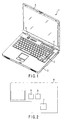
- the notebook PC 1 shown in FIG. 1 comprises a housing 3 having a keyboard 2 serving as an input operating portion provided on a top surface thereof, and a display panel 5 coupled to the housing 3 by hinges 4.
- a substrate 6 shown in FIG. 2 is built in the housing 3.
- An MPU 7, a bridge 8 and a VGA (Video Graphics Array) 9 are mounted on the substrate 6.
- the bridge 8 and the VGA 9 are an example of a circuit module which provided in the vicinity of the MPU 7. Load on each of the bridge 8 and the VGA 9 is varied in accordance with variation in load applied to the MPU 7. As the load increases, the amount of heat radiation is also increased.
- FIG. 2 shows an example of arrangement of the MPU 7, the bridge 8 and the VGA 9 on the substrate 6, and their arrangement is not limited to this.
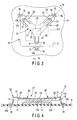
- a radiating unit 10 is attached to the bridge 8 and the VGA 9 as shown in FIG. 3.
- the radiating unit 10 comprises a radiating plate 11 which serves as a heat conducting member, and a retaining member 12 which fixes the radiating plate 11 to the substrate 6.
- the radiating plate 11 is shaped in a square which has round angles and which is larger than the bridge 8 and the VGA 9.
- An element portion 13 is provided at a central portion of the bridge 8 and the VGA 9.
- a heat transfer portion 11a of the radiating plate 11 is in close contact with an element portion 13 as shown in FIG. 4. It is preferable that a small gap formed between the radiating plate 11 and the element portion 13 is filled with a paste-like heat transfer material to improve the close contact between the radiating plate 11 and the element portion 13.
- a detailed shape of the radiating plate 11 is obtained by considering the amount of the heat input from the heat transfer portion 11a, the amount of the heat dissipation from an outer surface of the radiating plate 11, and a thermal conductivity of the radiating plate 11.
- the material of the radiating plate 11 aluminum, aluminum alloy, copper, silver, gold or the like with high thermal conductivity, is used.
- the retaining member 12 has three feet 14, 15 and 16, and a pressing portion 17 as shown in FIG. 3.
- the feet 14, 15 and 16 extend toward the substrate 6, so as to go around outer peripheral edges of the radiating plate 11. End portions 14a, 15a and 16a of the respective feet 14, 15 and 16 are fixed on the substrate 6 by screws 18 as shown in FIG. 4.
- the end portions 14a, 15a and 16a of the respective feet 14, 15 and 16 may be fixed on the substrate 6 by soldering, swaging, or insertion.
- the end portions 14a, 15a and 16a are arranged at positions corresponding to vertexes of a triangle including the element portion 13.
- one of the feet (first foot 14) is provided so as to go around one of sides extending straight, of the radiating plate 11.
- Remaining two feet (second foot 15 and third foot 16) are provided so as to go around corner portions 11b of the radiating plate 11, which are to be both ends of a side opposite to the side at which the first foot 14 is arranged.
- the pressing portion 17 has a contact portion 19 and urging portions 20.
- the contact portion 19 abuts on a pressed portion 11c which is provided to be opposite to the heat transfer portion 11a of the radiating plate 11.
- the urging portion 20 is provided between the contact portion 19 and each of feet 14, 15 and 16.
- the pressing portion 17 is provided in a shape in which the urging portions 20 extend radially from the contact portion 19.
- the urging portions 20 are bent in a direction away from the radiating plate 11, in the middle of the contact portion 19 and the feet 14, 15 and 16 as shown in FIG. 4.
- the feet 14, 15 and 16 are provided continuously with the urging portions 20. Therefore, the retaining member 12 becomes capable of urging the radiating plate 11 toward the element portion 13 by fixing the feet 14, 15 and 16 on the substrate 6.
- Cutout ends 21 near the feet 14, 15 and 16 are connected to the radiating plate 11 by eyelets 22.
- the cutout ends 21 and the radiating plate 11 may be connected not by the eyelets 22, but by spot welding, laser welding, swaging or the like. Even if the cutout ends 21 are not connected they have the function of the present invention.
- the radiating unit 10 is attached to the bridge 8 and the VGA 9 serving as the circuit modules. Therefore, as the load of the MPU 7 is increased, heat generated in the element portions 13 of the bridge 8 and the VGA 9 is transmitted from the heat transfer portion 11a to the radiating plate 11. The heat transmitted to the radiating plate 11 is radiated from the outer peripheral surface thereof.
- the radiating unit 10 is fixed to the substrate 6 by three feet 14, 15 and 16. In other words, the occupied area required to attach the radiating unit 10 to the substrate 6 is smaller as compared with a cooler fixed at four positions. The flexibility of designing of the wiring on the substrate 6 is thereby increased.
- a radiating unit 10b shown in FIG. 5 is different from the radiating unit of the first embodiment with respect to the arrangement of the feet 14, 15 and 16.
- the first foot 14 is provided so as to go around one of the sides of the radiating plate 11 as shown in FIG. 5.
- the end portion 14a of the first foot 14 is provided in a direction away from the element portion 13.
- the second foot 15 and the third foot 16 are provided so as to go around the corner portions 11b of the radiating plate 11.
- the end portion 15a of the second foot 15 and the end portion 16a of the third foot 16 are formed toward an opposite direction to the end portion 14a of the first foot 14.
- the end portions 14a, 15a ands 16a project from two parallel sides of the radiating plate 11 shaped in a square. None projects from sides which extend in a direction crossing the sides from which the end portions 14a, 15a and 16a project. Therefore, even if the bridge 8 and the VGA 9 serving as the circuit modules are arranged near an edge 6a of the substrate 6, the radiating unit 10b can be attached to the bridge 8 and the VGA 9 by arranging the end portions 14a, 15a and 16a along the edge 6a of the substrate 6.
- a radiating unit 10c shown in FIG. 6 is different from the radiating unit of the first and second embodiments with respect to the arrangement of the feet 14, 15 and 16.
- the first foot 14 is provided so as to go around one of the sides of the radiating plate 11 as shown in FIG. 6.
- the end portion 14a of the first foot 14 is provided in a direction of leaving from the element portion 13.
- the second foot 15 and the third foot 16 are provided so as to go around the corner portions 11b of the radiating plate 11.
- the end portion 15a of the second foot 15 and the end portion 16a of the third foot 16 are formed in a direction of separating from each other, along a direction which crosses the extending direction of the end portion 14a of the first foot 14.
- the radiating unit 10c described above nothing projects from the opposite edge to the side at which the first foot 14 is arranged, of the radiating plate 11 shaped in a square. Therefore, even if the other module or a unit U is arranged side by side with the bridge 8 and the VGA 9, on the substrate 6, the radiating unit 10c can be attached to the bridge 8 and the VGA 9 by making the side from which the foot 14, 15 or 16 does not projects face the other module or the unit U.
- the radiating unit 10b of the second embodiment can be attached to the bridge 8 and the VGA 9 arranged in the vicinity of the other module or the unit U, similarly to the radiating unit 10c of the third embodiment.
- the radiating unit 10c of the third embodiment can also be attached to the bridge 8 and the VGA 9 arranged in the vicinity of the edge of the substrate 6, similarly to the radiating unit 10b of the second embodiment.
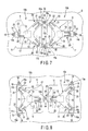
- FIG. 7 Elements having like or similar functions to those of the first to third embodiments are denoted by same reference numerals and a description thereof will be omitted.
- the bridge 8 and the VGA 9 are arranged closely to each other, on the substrate 6, as shown in FIG. 7.
- the radiating unit 10b shown in FIG. 10 is adopted as a radiating unit attached to the bridge 8 and a radiating unit attached to the VGA 9.
- the end portion 15a of the second foot 15 of one of the radiating unit and the end portion 16a of the third foot 16 of another radiating unit are overlapped and fixed to the substrate 6, and the end portion 16a of the third foot 16 of one of the radiating unit and the end portion 15a of the second foot 15 of another radiating unit, are overlapped and fixed to the substrate 6.
- the second foot 15 and the third foot 16 of the radiating units 10b attached to the adjacent circuit modules are fixed to the same position on the substrate 6.
- the occupied area to be attached each radiating unit 10b to the substrate 6 can be therefore made smaller.
- the attachment of the radiating units 10b can be simplified if a radiating unit having the end portion 15a of the second foot 15 of one of the radiating units 10b and the end portion 16a of the third foot 16 of the other radiating unit 10b coupled continuously is provided instead of respectively providing the radiating units 10b on the bridge 8 and the VGA 9, and sharing the positions of the fixed feet thereof.
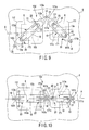
- FIG. 8 Elements having like or similar functions to those of the first to fourth embodiments are denoted by same reference numerals and a description thereof will be omitted.
- the radiating unit 10c shown in FIG. 6 is adopted as radiating unit attached to the adjacent circuit modules.
- the radiating units 10c are fixed on the substrate 6 such that the end portions 14a of the first feet 14 of the radiating units 10c are overlapped.
- the occupied area for attaching each radiating unit 10c on the substrate 6 can be made smaller by fixing at least one of the feet of the radiating unit 10c, i.e. the first foot 14 in this case, at a common position.
- the assembling operation of the radiating unit can be simplified if a radiating unit continuously formed at the end portions such as the end portions 14a of the first feet 14 of the radiating units 10c is provided instead of respectively attaching the radiating unit 10c to the bridge 8 and the VGA 9, and sharing the positions of the fixed feet thereof.
- the bridge 8 and the VGA 9 can be arranged side by side, in the vicinity of other adjacent units or modules, by attaching the radiating units 10c to the bridge 8 and the VGA 9.
- the wiring between the bridge 8 and the VGA 9, extending to other electronic components mounted on the substrate 6, can easily be arranged.
- FIG. 9 Elements having like or similar functions to those of the first to fifth embodiments are denoted by same reference numerals and a description thereof will be omitted.
- the bridge 8 serving as the first circuit module and the VGA 9 serving as the second circuit module are mounted side by side on the substrate 6 as shown in FIG. 9.
- a radiating unit 10d is attached to the bridge 8 and the VGA 9, respectively.
- the radiating unit 10d has a first radiating plate 111 serving as a first heat conducting member, a second radiating plate 112 serving as a second heat conducting member, and a retaining member 121.
- the first radiating plate 111 has a heat transfer portion 111a which is in close contact with a first element portion 13a exposed from the bridge 8.
- the second radiating plate 112 has a heat transfer portion 112a which is in close contact with a second element portion 13b exposed from the VGA 9.
- the first radiating plate 111 and the second radiating plate 112 are formed to be one size larger than the bridge 8 and the VGA 9, respectively.
- the retaining member 121 has a first pressing portion 171 and a second pressing portion 172.
- a fixing portion 23 is provided at a position adjacent to both the bridge 8 and the VGA 9.
- the first pressing portion 171 is arranged in a direction of crossing the first element portion 13a of the bridge 8 from the fixing portion 23.
- the second pressing portion 172 is arranged in a direction of crossing the second element portion 13b of the VGA 9 from the fixing portion 23.
- An end portion 171a of a foot 141a of the first pressing portion 171 and an end portion 172a of a foot 142a of the second pressing portion 172 are provided continuously and fixed to the fixing portion 23 by the screw 18.
- An end portion 171b of a foot 141b of the first pressing portion 171 is fixed to the substrate 6 by the screw 18, at a position passed over the first radiating plate 111.
- An end portion 172b of a foot 142b of the second pressing portion 172 is fixed to the substrate 6 by the screw 18, at a position passed over the second radiating plate 112.
- the fixing portion 23 is provided at a position remote from a line A extending in a direction in which the first element portion 13a and the second element portion 13b are aligned. Therefore, the end portion 171b of the first pressing portion 171 and the end portion 172b of the second pressing portion 172 are fixed to the substrate 6, on an opposite to the fixing portion 23 about the line A.
- Each of the first pressing portion 171 and the second pressing portion 172 has the contact portion 19 and the urging portion 20.
- the contact portion 19 of the first pressing portion 171 abuts on an area of the opposite to the heat transfer portion 111a of the first radiating plate 111.
- the contact portion 19 of the second pressing portion 172 abuts on an area of the opposite to the heat transfer portion 112a of the second radiating plate 112.
- the urging portion 20 of the first pressing portion 171 is provided at a position of both sides of the first element portion 13a, specifically a position between the contact portion 19 and the feet 141a, 141b.
- the urging portion 20 of the second pressing portion 172 is provided at a position of both sides of the second element portion 13b, specifically a position between the contact portion 19 and the feet 142a, 142b.
- the first radiating plate 111 which is in close contact with the first element portion 13a of the bridge 8, and the second radiating plate 112 which is in close contact with the second element portion 13b of the VGA 9, are fixed on the substrate 6 by both the end portions 171a, 171b of the first pressing portion 171 and both the end portions 172a, 172b of the second pressing portion 172, respectively.
- the end portion 171a of the first pressing portion 171 and the end portion 172a of the second pressing portion 172 are provided continuously and fixed on the fixing portion 23. In other words, the radiating unit attached to two circuit modules is fixed at three positions.
- the occupied area required to attach the radiating unit 10d to the substrate 6 is smaller as compared with a case where radiating units are attached to respective circuit modules. In other words, the flexibility of the wiring on the substrate 6 is thereby increased.
- a seventh embodiment according to the present invention will be described with reference to FIG. 10. Elements having like or similar functions to those of the first to sixth embodiments are denoted by same reference numerals and a description thereof will be omitted.
- the seventh embodiment is different from the sixth embodiment, with respect to the feature that the first pressing portion 171 and the second pressing portion 172 are arranged linearly along the line A, in opposite directions to each other about the fixing portion 23, as shown in FIG. 10.
- the first pressing portion 171 and the second pressing portion 172 are formed continuously, but may be formed separately. Overlapping the end portions 171a and 172a on the fixing portion 23 is substantially of no functional difference from unitedly forming the end portions 171a and 172a.
- the feet 141a, 141b and the feet 142a, 142b are provided so as to go around the opposite corner portions of the respective radiating plates 111 and 112 in the sixth embodiment, while the feet are provided so as to go around the opposite sides of the respective radiating plates 111 and 112 in the seventh embodiment. However, the feet may be provided so as to go around the opposite corner portions of the radiating plate 111 and so as to go around the opposite sides of the radiating plate 112, and vice versa.
- a radiating unit 10e is attached to the bridge 8 and the VGA 9.
- the radiating unit 10e has the first pressing portion 171 and the second pressing portion 172.
- the end portion 171a of the first pressing portion 171 and the end portion 172a of the second pressing portion 172 which are considered as the proximal portions of the respective pressing portions, are supported between the bridge 8 and the VGA 9.
- the end portion 171a and the end portion 172a are formed sequentially on a common plane.
- End portions 174 and 175 are formed to extend from a connecting portion 173 provided between the end portions 171a and 172a, along a space between the bridge 8 and the VGA 9.
- End portions 174a and 175a of the respective feet 174 and 175 are fixed on the substrate 6 by the screws 18.
- the urging portions 20 are formed in the middle parts of the first pressing portion 171 and the second pressing portion 172, respectively.
- the contact portions 19 are provided at distal portion 171c of the first pressing portion 171 and the distal portion 172c of the second pressing portion 172, respectively.
- the distal portion 171c is pushed on a portion of the opposite to the heat transfer portion 111a of the radiating plate 111.
- the distal portion 172c is pushed on a portion of the opposite to the heat transfer portion 112a of the radiating plate 112.
- the distal portions 171c and 172c may be attached and fixed to the respective radiating plates 111 and 112 by spot welding or laser welding, or the other method such as swaging, rivets, eyelets or the like, or may be pushed and retained by an urging force.
- the heat generated at the bridge 8 and the VGA 9 is transferred to the radiating plates 111 and 112 through the heat transfer portions 111a and 112a.
- the radiating unit 10e is merely fixed at two positions for two circuit modules.
- the occupied area required to attach the radiating unit 10e to the substrate 6 is therefore smaller as compared with a case where radiating units are attached to respective circuit modules.
- the connecting portion 173 is arranged between two circuit modules, i.e. the bridge 8 and the VGA 9, each of the radiating plates 111 and 112 can be urged with a substantially even urging force.
- FIG. 12 Elements having like or similar functions to those of the first to eighth embodiments are denoted by same reference numerals and a description thereof will be omitted.
- a radiating unit 10f is attached to the bridge 8 and the VGA 9 as shown in FIG. 12.
- the radiating unit 10f has the first pressing portion 171 and the second pressing portion 172.
- the end portions 171a and 172a are fixed at the fixing portion 23, which is provided on the substrate 6, between the bridge 8 and the VGA 9.
- the first pressing portion 171 and the second pressing portion 172 may be provided separately or formed unitedly at the end portions 171a and 172a.
- the radiating unit 10f has a structure which is omitted the end portions 171b and 172b from the radiating unit 10d of the seventh embodiment. In other words, the radiating unit 10f is fixed at only one position on the substrate 6. The occupied area required to attach the radiating unit 10f to the substrate 6 is therefore smaller as compared with a case where radiating units are attached to two circuit modules, respectively.
- the bridge 8 and the VGA 9 have been explained as the circuit modules.
- the present invention may be applied to the other circuit module such as the MPU 7.
- the occupied area required to attach the radiating unit to the substrate 6 can be therefore smaller by attaching the radiating units as described in the fourth to ninth embodiments to the respective circuit modules.
- the heat conducting member may be formed integrally with a heat sink or thermally connected to a heat sink formed as another member. Furthermore, the heat conducting member may be thermally connected to a fan module having a radiating member.
Landscapes
- Physics & Mathematics (AREA)
- Condensed Matter Physics & Semiconductors (AREA)
- General Physics & Mathematics (AREA)
- Engineering & Computer Science (AREA)
- Computer Hardware Design (AREA)
- Microelectronics & Electronic Packaging (AREA)
- Power Engineering (AREA)
- Cooling Or The Like Of Electrical Apparatus (AREA)
- Cooling Or The Like Of Semiconductors Or Solid State Devices (AREA)
Applications Claiming Priority (2)
| Application Number | Priority Date | Filing Date | Title |
|---|---|---|---|
| JP2003399818 | 2003-11-28 | ||
| JP2003399818A JP4387777B2 (ja) | 2003-11-28 | 2003-11-28 | 電子機器 |
Publications (3)
| Publication Number | Publication Date |
|---|---|
| EP1536467A2 true EP1536467A2 (de) | 2005-06-01 |
| EP1536467A3 EP1536467A3 (de) | 2007-06-13 |
| EP1536467B1 EP1536467B1 (de) | 2009-04-15 |
Family
ID=34463889
Family Applications (1)
| Application Number | Title | Priority Date | Filing Date |
|---|---|---|---|
| EP04028029A Active EP1536467B1 (de) | 2003-11-28 | 2004-11-25 | Halter und Wärmeleiter für Elektroniktbauteil |
Country Status (4)
| Country | Link |
|---|---|
| US (1) | US7170750B2 (de) |
| EP (1) | EP1536467B1 (de) |
| JP (1) | JP4387777B2 (de) |
| DE (1) | DE602004020569D1 (de) |
Cited By (4)
| Publication number | Priority date | Publication date | Assignee | Title |
|---|---|---|---|---|
| FR2931523A1 (fr) * | 2008-05-21 | 2009-11-27 | Fagorbrandt Sas | Dispositif de fixation de composants et appareil electromenager associe |
| EP2445005A1 (de) * | 2010-10-22 | 2012-04-25 | Siemens Aktiengesellschaft | Kühlvorrichtung mit Flachfeder |
| WO2012113584A1 (de) * | 2011-02-22 | 2012-08-30 | Infineon Technologies Bipolar Gmbh & Co. Kg | Leistungshalbleitermodul |
| EP2927954A1 (de) * | 2014-04-02 | 2015-10-07 | Brusa Elektronik AG | Befestigungssystem für ein Leistungsmodul |
Families Citing this family (37)
| Publication number | Priority date | Publication date | Assignee | Title |
|---|---|---|---|---|
| CN100546019C (zh) * | 2005-04-15 | 2009-09-30 | 富士通株式会社 | 散热器、电路基板、电子设备 |
| US7570490B2 (en) * | 2005-08-31 | 2009-08-04 | Ati Technologies Ulc | Variable spring rate thermal management apparatus attachment mechanism |
| US7400507B2 (en) * | 2005-10-19 | 2008-07-15 | Inventec Corporation | Fastening structure |
| JP4095641B2 (ja) * | 2006-01-31 | 2008-06-04 | 株式会社東芝 | 電子機器 |
| JP4816189B2 (ja) * | 2006-03-27 | 2011-11-16 | 日本電気株式会社 | 放熱構造、情報装置および放熱構造の製造方法 |
| US7460371B2 (en) * | 2006-05-25 | 2008-12-02 | Agilent Technologies, Inc. | Wiffle tree components, cooling systems, and methods of attaching a printed circuit board to a heat sink |
| JP4921096B2 (ja) * | 2006-09-28 | 2012-04-18 | 富士通株式会社 | 電子機器および冷却部品 |
| US7782622B1 (en) * | 2006-10-04 | 2010-08-24 | Nvidia Corporation | Attachment apparatus for electronic boards |
| US7436673B2 (en) * | 2006-11-30 | 2008-10-14 | Inventec Corporation | Heat sink fixing assembly |
| US7554809B2 (en) * | 2007-02-09 | 2009-06-30 | Inventec Corporation | Heatsink assembly structure |
| JP2008251687A (ja) * | 2007-03-29 | 2008-10-16 | Toshiba Corp | プリント回路板、およびこれを備えた電子機器 |
| US7589972B2 (en) * | 2007-05-26 | 2009-09-15 | Hon Hai Precision Ind. Co., Ltd. | Electrical connector with clip mechanism |
| CN101377706B (zh) * | 2007-08-31 | 2011-12-21 | 鸿富锦精密工业(深圳)有限公司 | 电脑散热器背板组合 |
| TWI402660B (zh) * | 2007-09-28 | 2013-07-21 | Hon Hai Prec Ind Co Ltd | 電腦散熱器背板組合及具有該背板組合之散熱模組 |
| JP2009151367A (ja) * | 2007-12-18 | 2009-07-09 | Toshiba Corp | 電子機器 |
| US7764493B2 (en) * | 2008-01-04 | 2010-07-27 | Apple Inc. | Systems and methods for cooling electronic devices using airflow dividers |
| JP2010087044A (ja) | 2008-09-29 | 2010-04-15 | Toshiba Corp | 電子機器 |
| JP2015038897A (ja) * | 2009-03-30 | 2015-02-26 | 株式会社東芝 | 電子機器 |
| JP2011128708A (ja) * | 2009-12-15 | 2011-06-30 | Toshiba Corp | 電子機器 |
| JP2011166024A (ja) * | 2010-02-12 | 2011-08-25 | Toshiba Corp | 電子機器 |
| US8233280B2 (en) * | 2010-03-15 | 2012-07-31 | Lincoln Global, Inc. | Electronic module with center mounting fasteners |
| JP4869419B2 (ja) * | 2010-03-18 | 2012-02-08 | 株式会社東芝 | 電子機器 |
| JP4875181B2 (ja) | 2010-04-09 | 2012-02-15 | 株式会社東芝 | 電子機器 |
| JP4843725B1 (ja) * | 2010-06-18 | 2011-12-21 | 株式会社東芝 | テレビジョン装置および電子機器 |
| BR112013007422B1 (pt) * | 2010-09-29 | 2019-11-12 | Siemens Ag | sistema de controle submarinho |
| TWI514953B (zh) * | 2011-08-09 | 2015-12-21 | Asustek Comp Inc | 散熱模組 |
| TWI538611B (zh) * | 2011-11-29 | 2016-06-11 | 鴻準精密工業股份有限公司 | 散熱裝置及其扣具 |
| JP5242817B1 (ja) | 2012-01-31 | 2013-07-24 | 株式会社東芝 | 電子機器 |
| JP2014016026A (ja) * | 2012-06-13 | 2014-01-30 | Toyota Industries Corp | 板ばねおよび放熱装置 |
| WO2014147681A1 (ja) * | 2013-03-22 | 2014-09-25 | パナソニック株式会社 | 実装基板、押圧部材、電子機器 |
| JP6201511B2 (ja) * | 2013-08-15 | 2017-09-27 | 富士通株式会社 | 電子機器 |
| JP6898162B2 (ja) * | 2017-06-23 | 2021-07-07 | 矢崎総業株式会社 | 電子部品の固定構造 |
| US10721840B2 (en) * | 2017-10-11 | 2020-07-21 | DISH Technologies L.L.C. | Heat spreader assembly |
| TWM567398U (zh) * | 2018-06-04 | 2018-09-21 | 華碩電腦股份有限公司 | 電路板及其散熱裝置 |
| US11251103B2 (en) * | 2019-03-29 | 2022-02-15 | Intel Corporation | Segmented heatsink |
| JP6979095B2 (ja) * | 2020-02-20 | 2021-12-08 | レノボ・シンガポール・プライベート・リミテッド | 熱輸送装置および電子機器 |
| US11800687B2 (en) | 2021-08-26 | 2023-10-24 | Dish Network L.L.C. | Heat transfer assembly |
Citations (2)
| Publication number | Priority date | Publication date | Assignee | Title |
|---|---|---|---|---|
| US6222734B1 (en) | 1999-11-29 | 2001-04-24 | Intel Corporation | Clamping heat sinks to circuit boards over processors |
| JP2003101272A (ja) | 2001-09-21 | 2003-04-04 | Toshiba Corp | 冷却装置及び冷却装置を内蔵した電子機器 |
Family Cites Families (75)
| Publication number | Priority date | Publication date | Assignee | Title |
|---|---|---|---|---|
| WO1985003385A1 (fr) * | 1984-01-23 | 1985-08-01 | La Telemecanique Electrique | Dispositif de montage et de connexion pour semi-conducteurs de puissance |
| US5089936A (en) * | 1988-09-09 | 1992-02-18 | Hitachi, Ltd. | Semiconductor module |
| US5268817A (en) | 1990-04-27 | 1993-12-07 | Kabushiki Kaisha Toshiba | Portable computer with keyboard and having display with coordinate input tablet rotatably mounted to face either toward or away from keyboard when closed over keyboard |
| EP0654176B1 (de) * | 1993-06-07 | 1998-05-20 | Melcher Ag | Befestigungsvorrichtung für halbleiter-schaltelemente |
| JPH0749725A (ja) | 1993-08-06 | 1995-02-21 | Sharp Corp | 情報処理装置 |
| JP3385482B2 (ja) | 1993-11-15 | 2003-03-10 | 株式会社日立製作所 | 電子機器 |
| JP3392527B2 (ja) | 1994-08-01 | 2003-03-31 | 富士通株式会社 | ヒートシンクの取付構造及び固定具 |
| JP3258198B2 (ja) | 1995-04-28 | 2002-02-18 | 株式会社東芝 | 回路モジュールの冷却装置およびこの冷却装置を有する携帯形電子機器 |
| EP0834795B1 (de) | 1995-06-08 | 2002-01-02 | International Business Machines Corporation | Mechanische struktur einer informationsverarbeitungsvorrichtung |
| US6094180A (en) | 1996-04-05 | 2000-07-25 | Fakespace, Inc. | Gimbal-mounted virtual reality display system |
| JPH104161A (ja) | 1996-06-14 | 1998-01-06 | Nippon Keiki Seisakusho:Kk | ヒートシンク取り付け装置 |
| JPH1055227A (ja) | 1996-08-09 | 1998-02-24 | Sharp Corp | 情報処理装置 |
| JPH10189843A (ja) * | 1996-12-25 | 1998-07-21 | Ricoh Co Ltd | 電子部品押え金具 |
| JPH10261884A (ja) | 1997-03-17 | 1998-09-29 | Nec Home Electron Ltd | 情報処理装置の冷却構造 |
| JPH10303582A (ja) | 1997-04-22 | 1998-11-13 | Toshiba Corp | 回路モジュールの冷却装置および回路モジュールを搭載した携帯形情報機器 |
| JPH1139058A (ja) | 1997-07-14 | 1999-02-12 | Ricoh Co Ltd | ペン入力型電子機器 |
| US6005767A (en) | 1997-11-14 | 1999-12-21 | Vadem | Portable computer having articulated display |
| US20020053421A1 (en) | 1997-09-10 | 2002-05-09 | Kabushiki Kaisha Toshiba | Heat dissipating structure for electronic apparatus |
| KR100286375B1 (ko) | 1997-10-02 | 2001-04-16 | 윤종용 | 전자 시스템의 방열장치 및 방열장치가 사용된 컴퓨터 시스템 |
| US6049459A (en) * | 1997-11-17 | 2000-04-11 | Lucent Technologies, Inc. | Nesting clamps for electrical components |
| JPH11166500A (ja) | 1997-12-03 | 1999-06-22 | Toshiba Ave Co Ltd | ポンプ |
| US6464195B1 (en) | 1997-12-04 | 2002-10-15 | Raymond Hildebrandt | Ergonomic mounting for computer screen displays |
| JP3366244B2 (ja) | 1998-02-04 | 2003-01-14 | 富士通株式会社 | 電子機器 |
| JP4128660B2 (ja) | 1998-07-27 | 2008-07-30 | 株式会社東芝 | 電子機器 |
| US6282082B1 (en) | 1998-07-31 | 2001-08-28 | Qubit, Llc | Case for a modular tablet computer system |
| US6377452B1 (en) | 1998-12-18 | 2002-04-23 | Furukawa Electric Co., Ltd. | Heat pipe hinge structure for electronic device |
| US6483445B1 (en) | 1998-12-21 | 2002-11-19 | Intel Corporation | Electronic device with hidden keyboard |
| GB2348459B (en) | 1999-03-27 | 2003-03-19 | Ibm | Lid restraint for portable computer |
| US6231371B1 (en) | 1999-06-25 | 2001-05-15 | Hewlett-Packard Company | Docking station for multiple devices |
| JP4270667B2 (ja) | 1999-08-17 | 2009-06-03 | 株式会社東芝 | 回路部品の冷却装置および電子機器 |
| JP3283853B2 (ja) | 1999-09-17 | 2002-05-20 | 米沢日本電気株式会社 | ドッキングステーション |
| US6166907A (en) | 1999-11-26 | 2000-12-26 | Chien; Chuan-Fu | CPU cooling system |
| US6196850B1 (en) | 2000-02-10 | 2001-03-06 | International Business Machines Corporation | Rotatable docking station for an electronic device |
| JP2001230356A (ja) | 2000-02-17 | 2001-08-24 | Showa Denko Kk | クリップ付き放熱器 |
| JP2001251079A (ja) | 2000-03-03 | 2001-09-14 | Diamond Electric Mfg Co Ltd | ヒートパイプを用いたヒートシンクとヒートパイプの製造方法 |
| US6418017B1 (en) | 2000-03-30 | 2002-07-09 | Hewlett-Packard Company | Heat dissipating chassis member |
| US6430038B1 (en) | 2000-04-18 | 2002-08-06 | Hewlett-Packard Company | Computer with articulated mechanism |
| US6437973B1 (en) | 2000-04-18 | 2002-08-20 | Hewlett-Packard Company | Modular mechanism for movable display |
| US6313990B1 (en) | 2000-05-25 | 2001-11-06 | Kioan Cheon | Cooling apparatus for electronic devices |
| JP3302350B2 (ja) | 2000-06-29 | 2002-07-15 | 株式会社東芝 | 電子機器 |
| US6296048B1 (en) | 2000-09-08 | 2001-10-02 | Powerwave Technologies, Inc. | Heat sink assembly |
| JP2002099356A (ja) | 2000-09-21 | 2002-04-05 | Toshiba Corp | 電子機器用冷却装置および電子機器 |
| US6469893B1 (en) * | 2000-09-29 | 2002-10-22 | Intel Corporation | Direct heatpipe attachment to die using center point loading |
| US6396687B1 (en) | 2000-10-13 | 2002-05-28 | Dell Products, L.P. | Rotating portable computer docking station |
| JP3607608B2 (ja) | 2000-12-19 | 2005-01-05 | 株式会社日立製作所 | ノート型パソコンの液冷システム |
| US6717798B2 (en) | 2001-03-22 | 2004-04-06 | Intel Corporation | Docking digital picture displays |
| US20020141159A1 (en) | 2001-03-29 | 2002-10-03 | Bloemen James Andrew | Sealed and passively cooled telecommunications customer service terminal |
| JP2002344186A (ja) | 2001-05-15 | 2002-11-29 | Sharp Corp | 電子機器 |
| JP2002353670A (ja) | 2001-05-25 | 2002-12-06 | Toshiba Home Technology Corp | ヒートシンク装置 |
| FR2827115B1 (fr) | 2001-07-06 | 2003-09-05 | Alstom | Coffre pour convertisseur de puissance |
| TW558611B (en) | 2001-07-18 | 2003-10-21 | Matsushita Electric Ind Co Ltd | Small pump, cooling system and portable equipment |
| US6480373B1 (en) | 2001-07-24 | 2002-11-12 | Compaq Information Technologies Group, L.P. | Multifunctional foldable computer |
| US6873521B2 (en) | 2001-07-24 | 2005-03-29 | Hewlett-Packard Development Company, L.P. | Multiple environment foldable computer |
| JP2003044169A (ja) | 2001-07-31 | 2003-02-14 | Casio Comput Co Ltd | 電子機器 |
| JP4512296B2 (ja) | 2001-08-22 | 2010-07-28 | 株式会社日立製作所 | 可搬型情報処理装置の液冷システム |
| JP3925126B2 (ja) | 2001-08-28 | 2007-06-06 | 日産自動車株式会社 | 燃料電池 |
| JP2003078270A (ja) | 2001-09-07 | 2003-03-14 | Hitachi Ltd | 電子装置 |
| JP3946018B2 (ja) | 2001-09-18 | 2007-07-18 | 株式会社日立製作所 | 液冷却式回路装置 |
| JP3741092B2 (ja) | 2001-09-25 | 2006-02-01 | 松下電器産業株式会社 | 超薄型ポンプとこれを備えた冷却システム |
| JP2003223238A (ja) | 2002-01-28 | 2003-08-08 | Internatl Business Mach Corp <Ibm> | コンピュータ装置、モニタユニットおよび対面ユニットの支持構造物 |
| JP3961843B2 (ja) | 2002-02-08 | 2007-08-22 | 株式会社日立製作所 | 液体冷却システムを有する小型電子計算機 |
| JP3452059B1 (ja) | 2002-05-15 | 2003-09-29 | 松下電器産業株式会社 | 冷却装置とそれを備えた電子機器 |
| JP3431024B1 (ja) | 2003-01-15 | 2003-07-28 | 松下電器産業株式会社 | 冷却装置 |
| JP4168669B2 (ja) | 2002-05-31 | 2008-10-22 | 松下電工株式会社 | 薄型ポンプ |
| DE10225993A1 (de) * | 2002-06-12 | 2003-12-24 | Bosch Gmbh Robert | Kühlkörper |
| US6856506B2 (en) | 2002-06-19 | 2005-02-15 | Motion Computing | Tablet computing device with three-dimensional docking support |
| KR100891994B1 (ko) * | 2002-06-20 | 2009-04-08 | 삼성전자주식회사 | 히트싱크 고정장치 |
| US6788530B2 (en) | 2002-09-24 | 2004-09-07 | International Business Machines Corporation | User friendly computer equipment, monitor unit, and monitor unit setting base |
| DE60209423T2 (de) * | 2002-11-08 | 2006-08-10 | Agilent Technologies Inc., A Delaware Corp., Palo Alto | Mikrochip-Kühlung auf Leiterplatte |
| JP2003216278A (ja) | 2002-12-10 | 2003-07-31 | Toshiba Corp | 電子機器 |
| JP2004348650A (ja) | 2003-05-26 | 2004-12-09 | Toshiba Corp | 電子機器 |
| US7035090B2 (en) | 2003-09-04 | 2006-04-25 | Kabushiki Kaisha Toshiba | Interlocking mechanism for a display |
| JP2005107122A (ja) | 2003-09-30 | 2005-04-21 | Toshiba Corp | 電子機器 |
| JP2005190316A (ja) | 2003-12-26 | 2005-07-14 | Toshiba Corp | 電子機器 |
| US7095614B2 (en) * | 2004-04-20 | 2006-08-22 | International Business Machines Corporation | Electronic module assembly |
-
2003
- 2003-11-28 JP JP2003399818A patent/JP4387777B2/ja not_active Expired - Lifetime
-
2004
- 2004-11-22 US US10/994,938 patent/US7170750B2/en active Active
- 2004-11-25 DE DE602004020569T patent/DE602004020569D1/de active Active
- 2004-11-25 EP EP04028029A patent/EP1536467B1/de active Active
Patent Citations (2)
| Publication number | Priority date | Publication date | Assignee | Title |
|---|---|---|---|---|
| US6222734B1 (en) | 1999-11-29 | 2001-04-24 | Intel Corporation | Clamping heat sinks to circuit boards over processors |
| JP2003101272A (ja) | 2001-09-21 | 2003-04-04 | Toshiba Corp | 冷却装置及び冷却装置を内蔵した電子機器 |
Cited By (5)
| Publication number | Priority date | Publication date | Assignee | Title |
|---|---|---|---|---|
| FR2931523A1 (fr) * | 2008-05-21 | 2009-11-27 | Fagorbrandt Sas | Dispositif de fixation de composants et appareil electromenager associe |
| EP2445005A1 (de) * | 2010-10-22 | 2012-04-25 | Siemens Aktiengesellschaft | Kühlvorrichtung mit Flachfeder |
| WO2012113584A1 (de) * | 2011-02-22 | 2012-08-30 | Infineon Technologies Bipolar Gmbh & Co. Kg | Leistungshalbleitermodul |
| EP2927954A1 (de) * | 2014-04-02 | 2015-10-07 | Brusa Elektronik AG | Befestigungssystem für ein Leistungsmodul |
| US9497876B2 (en) | 2014-04-02 | 2016-11-15 | Brusa Elektronik Ag | Fastening systems for power modules |
Also Published As
| Publication number | Publication date |
|---|---|
| US20050117307A1 (en) | 2005-06-02 |
| EP1536467B1 (de) | 2009-04-15 |
| EP1536467A3 (de) | 2007-06-13 |
| US7170750B2 (en) | 2007-01-30 |
| JP2005166715A (ja) | 2005-06-23 |
| JP4387777B2 (ja) | 2009-12-24 |
| DE602004020569D1 (de) | 2009-05-28 |
Similar Documents
| Publication | Publication Date | Title |
|---|---|---|
| EP1536467A2 (de) | Halter und Wärmeleiter für Elektroniktbauteil | |
| US8125783B2 (en) | Printed circuit board and electronic apparatus | |
| US5557500A (en) | Heat dissipating arrangement in a portable computer | |
| US7674985B2 (en) | Printed wiring board assembly, method of mounting components on printed wiring board and electronic apparatus | |
| US7091586B2 (en) | Detachable on package voltage regulation module | |
| EP2472352A2 (de) | Kühlvorrichtung und elektronische Vorrichtung | |
| JP2001345405A (ja) | 回路モジュール及び回路モジュールを搭載した電子機器 | |
| US20080130234A1 (en) | Electronic Apparatus | |
| US9357676B2 (en) | Cooling device and electronic apparatus | |
| US20050286229A1 (en) | Modular heat-dissipation assembly structure for a PCB | |
| US7333342B2 (en) | Fastening of a member pressing a heat sink against a component mounted on a circuit board | |
| JP2007234728A (ja) | 基板ユニット、およびこれを備えた冷却装置、並びに電子機器 | |
| US7110257B2 (en) | Electronic apparatus including printed wiring board provided with heat generating component | |
| US20100079951A1 (en) | Electronic apparatus | |
| JP2006114860A (ja) | 放熱装置 | |
| JP2008299628A (ja) | 電子機器、および冷却ユニット | |
| JP2009181215A (ja) | 電子機器 | |
| JP4956575B2 (ja) | 電子機器 | |
| US20080192439A1 (en) | Heatsink assembly structure | |
| JP2010021379A (ja) | 電子機器 | |
| US6064570A (en) | Computer processor/heat sink assembly having a dual direction air flow path | |
| JPH1098287A (ja) | 回路基板モジュールの冷却装置およびこの冷却装置を有する携帯形電子機器 | |
| US7864535B2 (en) | Electronic device | |
| WO2021186797A1 (ja) | 回路基板モジュール | |
| CN1745608A (zh) | 用于电子设备的散热装置 |
Legal Events
| Date | Code | Title | Description |
|---|---|---|---|
| PUAI | Public reference made under article 153(3) epc to a published international application that has entered the european phase |
Free format text: ORIGINAL CODE: 0009012 |
|
| 17P | Request for examination filed |
Effective date: 20041125 |
|
| AK | Designated contracting states |
Kind code of ref document: A2 Designated state(s): AT BE BG CH CY CZ DE DK EE ES FI FR GB GR HU IE IS IT LI LU MC NL PL PT RO SE SI SK TR |
|
| AX | Request for extension of the european patent |
Extension state: AL HR LT LV MK YU |
|
| PUAL | Search report despatched |
Free format text: ORIGINAL CODE: 0009013 |
|
| AK | Designated contracting states |
Kind code of ref document: A3 Designated state(s): AT BE BG CH CY CZ DE DK EE ES FI FR GB GR HU IE IS IT LI LU MC NL PL PT RO SE SI SK TR |
|
| AX | Request for extension of the european patent |
Extension state: AL HR LT LV MK YU |
|
| RIC1 | Information provided on ipc code assigned before grant |
Ipc: H05K 3/30 20060101ALI20070508BHEP Ipc: H01L 23/40 20060101AFI20050304BHEP |
|
| 17Q | First examination report despatched |
Effective date: 20070926 |
|
| AKX | Designation fees paid |
Designated state(s): DE FR GB |
|
| GRAP | Despatch of communication of intention to grant a patent |
Free format text: ORIGINAL CODE: EPIDOSNIGR1 |
|
| GRAS | Grant fee paid |
Free format text: ORIGINAL CODE: EPIDOSNIGR3 |
|
| GRAA | (expected) grant |
Free format text: ORIGINAL CODE: 0009210 |
|
| AK | Designated contracting states |
Kind code of ref document: B1 Designated state(s): DE FR GB |
|
| REG | Reference to a national code |
Ref country code: GB Ref legal event code: FG4D |
|
| REF | Corresponds to: |
Ref document number: 602004020569 Country of ref document: DE Date of ref document: 20090528 Kind code of ref document: P |
|
| PLBE | No opposition filed within time limit |
Free format text: ORIGINAL CODE: 0009261 |
|
| STAA | Information on the status of an ep patent application or granted ep patent |
Free format text: STATUS: NO OPPOSITION FILED WITHIN TIME LIMIT |
|
| 26N | No opposition filed |
Effective date: 20100118 |
|
| REG | Reference to a national code |
Ref country code: FR Ref legal event code: PLFP Year of fee payment: 12 |
|
| REG | Reference to a national code |
Ref country code: FR Ref legal event code: PLFP Year of fee payment: 13 |
|
| REG | Reference to a national code |
Ref country code: FR Ref legal event code: PLFP Year of fee payment: 14 |
|
| REG | Reference to a national code |
Ref country code: FR Ref legal event code: PLFP Year of fee payment: 15 |
|
| REG | Reference to a national code |
Ref country code: DE Ref legal event code: R082 Ref document number: 602004020569 Country of ref document: DE Representative=s name: HENKEL & PARTNER MBB PATENTANWALTSKANZLEI, REC, DE Ref country code: DE Ref legal event code: R082 Ref document number: 602004020569 Country of ref document: DE Representative=s name: PATENTANWAELTE HENKEL, BREUER & PARTNER MBB, DE Ref country code: DE Ref legal event code: R081 Ref document number: 602004020569 Country of ref document: DE Owner name: TOSHIBA CLIENT SOLUTIONS CO., LTD., JP Free format text: FORMER OWNER: KABUSHIKI KAISHA TOSHIBA, TOKIO/TOKYO, JP |
|
| REG | Reference to a national code |
Ref country code: GB Ref legal event code: 732E Free format text: REGISTERED BETWEEN 20190110 AND 20190116 |
|
| PGFP | Annual fee paid to national office [announced via postgrant information from national office to epo] |
Ref country code: GB Payment date: 20231123 Year of fee payment: 20 |
|
| PGFP | Annual fee paid to national office [announced via postgrant information from national office to epo] |
Ref country code: FR Payment date: 20231120 Year of fee payment: 20 Ref country code: DE Payment date: 20231121 Year of fee payment: 20 |