EP1450334B1 - Display device - Google Patents
Display device Download PDFInfo
- Publication number
- EP1450334B1 EP1450334B1 EP03701742A EP03701742A EP1450334B1 EP 1450334 B1 EP1450334 B1 EP 1450334B1 EP 03701742 A EP03701742 A EP 03701742A EP 03701742 A EP03701742 A EP 03701742A EP 1450334 B1 EP1450334 B1 EP 1450334B1
- Authority
- EP
- European Patent Office
- Prior art keywords
- substrate
- layer
- organic
- display device
- sealing
- Prior art date
- Legal status (The legal status is an assumption and is not a legal conclusion. Google has not performed a legal analysis and makes no representation as to the accuracy of the status listed.)
- Expired - Lifetime
Links
- 239000000758 substrate Substances 0.000 claims abstract description 184
- 238000007789 sealing Methods 0.000 claims abstract description 110
- 230000004888 barrier function Effects 0.000 claims abstract description 10
- 229910052782 aluminium Inorganic materials 0.000 claims description 20
- XAGFODPZIPBFFR-UHFFFAOYSA-N aluminium Chemical compound [Al] XAGFODPZIPBFFR-UHFFFAOYSA-N 0.000 claims description 20
- 239000000463 material Substances 0.000 claims description 17
- 230000002093 peripheral effect Effects 0.000 claims description 13
- 229920005989 resin Polymers 0.000 claims description 13
- 239000011347 resin Substances 0.000 claims description 13
- OYPRJOBELJOOCE-UHFFFAOYSA-N Calcium Chemical compound [Ca] OYPRJOBELJOOCE-UHFFFAOYSA-N 0.000 claims description 11
- 229910052791 calcium Inorganic materials 0.000 claims description 11
- 239000011575 calcium Substances 0.000 claims description 11
- 238000005304 joining Methods 0.000 claims description 10
- 238000004519 manufacturing process Methods 0.000 claims description 9
- 239000002313 adhesive film Substances 0.000 claims description 7
- 239000003566 sealing material Substances 0.000 claims 2
- 239000000853 adhesive Substances 0.000 abstract description 20
- 230000001070 adhesive effect Effects 0.000 abstract description 20
- 230000009467 reduction Effects 0.000 abstract description 3
- 239000000470 constituent Substances 0.000 abstract 1
- 239000010410 layer Substances 0.000 description 92
- 239000010408 film Substances 0.000 description 89
- 238000010586 diagram Methods 0.000 description 18
- 239000007789 gas Substances 0.000 description 18
- 238000000034 method Methods 0.000 description 18
- 238000009413 insulation Methods 0.000 description 13
- 230000008595 infiltration Effects 0.000 description 9
- 238000001764 infiltration Methods 0.000 description 9
- 229910052710 silicon Inorganic materials 0.000 description 9
- 239000010703 silicon Substances 0.000 description 9
- 230000008569 process Effects 0.000 description 8
- -1 acryl Chemical group 0.000 description 7
- 239000011229 interlayer Substances 0.000 description 7
- 230000001681 protective effect Effects 0.000 description 7
- XLYOFNOQVPJJNP-UHFFFAOYSA-N water Chemical compound O XLYOFNOQVPJJNP-UHFFFAOYSA-N 0.000 description 7
- 230000006866 deterioration Effects 0.000 description 6
- 239000012044 organic layer Substances 0.000 description 6
- 238000000059 patterning Methods 0.000 description 6
- 239000012298 atmosphere Substances 0.000 description 5
- QVGXLLKOCUKJST-UHFFFAOYSA-N atomic oxygen Chemical compound [O] QVGXLLKOCUKJST-UHFFFAOYSA-N 0.000 description 5
- 238000005229 chemical vapour deposition Methods 0.000 description 5
- 239000011521 glass Substances 0.000 description 5
- 229910052751 metal Inorganic materials 0.000 description 5
- 239000002184 metal Substances 0.000 description 5
- 229910052760 oxygen Inorganic materials 0.000 description 5
- 239000001301 oxygen Substances 0.000 description 5
- 239000010409 thin film Substances 0.000 description 5
- IJGRMHOSHXDMSA-UHFFFAOYSA-N Atomic nitrogen Chemical compound N#N IJGRMHOSHXDMSA-UHFFFAOYSA-N 0.000 description 4
- VYPSYNLAJGMNEJ-UHFFFAOYSA-N Silicium dioxide Chemical compound O=[Si]=O VYPSYNLAJGMNEJ-UHFFFAOYSA-N 0.000 description 4
- 230000005525 hole transport Effects 0.000 description 4
- 238000002347 injection Methods 0.000 description 4
- 239000007924 injection Substances 0.000 description 4
- 229920002521 macromolecule Polymers 0.000 description 4
- 230000003287 optical effect Effects 0.000 description 4
- 230000000007 visual effect Effects 0.000 description 4
- 238000001723 curing Methods 0.000 description 3
- 239000002274 desiccant Substances 0.000 description 3
- 238000005530 etching Methods 0.000 description 3
- 230000006870 function Effects 0.000 description 3
- 239000012535 impurity Substances 0.000 description 3
- 239000011159 matrix material Substances 0.000 description 3
- 230000035699 permeability Effects 0.000 description 3
- 229910021420 polycrystalline silicon Inorganic materials 0.000 description 3
- 229920005591 polysilicon Polymers 0.000 description 3
- 238000004544 sputter deposition Methods 0.000 description 3
- 239000004215 Carbon black (E152) Substances 0.000 description 2
- MYMOFIZGZYHOMD-UHFFFAOYSA-N Dioxygen Chemical compound O=O MYMOFIZGZYHOMD-UHFFFAOYSA-N 0.000 description 2
- 239000004698 Polyethylene Substances 0.000 description 2
- 239000004743 Polypropylene Substances 0.000 description 2
- 239000004793 Polystyrene Substances 0.000 description 2
- 229910004541 SiN Inorganic materials 0.000 description 2
- 230000005540 biological transmission Effects 0.000 description 2
- 239000000919 ceramic Substances 0.000 description 2
- 229910010293 ceramic material Inorganic materials 0.000 description 2
- 229910052681 coesite Inorganic materials 0.000 description 2
- 230000000052 comparative effect Effects 0.000 description 2
- 229910052906 cristobalite Inorganic materials 0.000 description 2
- 238000000151 deposition Methods 0.000 description 2
- 229910001873 dinitrogen Inorganic materials 0.000 description 2
- 229910001882 dioxygen Inorganic materials 0.000 description 2
- 230000003628 erosive effect Effects 0.000 description 2
- 230000002349 favourable effect Effects 0.000 description 2
- 229930195733 hydrocarbon Natural products 0.000 description 2
- 150000002430 hydrocarbons Chemical class 0.000 description 2
- 239000011261 inert gas Substances 0.000 description 2
- 229910010272 inorganic material Inorganic materials 0.000 description 2
- 239000011147 inorganic material Substances 0.000 description 2
- 150000002500 ions Chemical class 0.000 description 2
- 239000004973 liquid crystal related substance Substances 0.000 description 2
- 239000000203 mixture Substances 0.000 description 2
- 239000000178 monomer Substances 0.000 description 2
- 239000011368 organic material Substances 0.000 description 2
- 229920002120 photoresistant polymer Polymers 0.000 description 2
- 239000004033 plastic Substances 0.000 description 2
- 229920003023 plastic Polymers 0.000 description 2
- 229920000573 polyethylene Polymers 0.000 description 2
- 239000002861 polymer material Substances 0.000 description 2
- 229920001155 polypropylene Polymers 0.000 description 2
- 229920002223 polystyrene Polymers 0.000 description 2
- 239000002243 precursor Substances 0.000 description 2
- 238000012545 processing Methods 0.000 description 2
- 239000000377 silicon dioxide Substances 0.000 description 2
- 229910052814 silicon oxide Inorganic materials 0.000 description 2
- 238000004528 spin coating Methods 0.000 description 2
- 229910052682 stishovite Inorganic materials 0.000 description 2
- 229920001187 thermosetting polymer Polymers 0.000 description 2
- 229910052905 tridymite Inorganic materials 0.000 description 2
- 239000004925 Acrylic resin Substances 0.000 description 1
- ZOXJGFHDIHLPTG-UHFFFAOYSA-N Boron Chemical compound [B] ZOXJGFHDIHLPTG-UHFFFAOYSA-N 0.000 description 1
- OKTJSMMVPCPJKN-UHFFFAOYSA-N Carbon Chemical compound [C] OKTJSMMVPCPJKN-UHFFFAOYSA-N 0.000 description 1
- 229910052692 Dysprosium Inorganic materials 0.000 description 1
- 229910052691 Erbium Inorganic materials 0.000 description 1
- 229910052688 Gadolinium Inorganic materials 0.000 description 1
- 229910052779 Neodymium Inorganic materials 0.000 description 1
- OAICVXFJPJFONN-UHFFFAOYSA-N Phosphorus Chemical compound [P] OAICVXFJPJFONN-UHFFFAOYSA-N 0.000 description 1
- 229910052772 Samarium Inorganic materials 0.000 description 1
- 229910052581 Si3N4 Inorganic materials 0.000 description 1
- XUIMIQQOPSSXEZ-UHFFFAOYSA-N Silicon Chemical compound [Si] XUIMIQQOPSSXEZ-UHFFFAOYSA-N 0.000 description 1
- 229910052769 Ytterbium Inorganic materials 0.000 description 1
- 239000012790 adhesive layer Substances 0.000 description 1
- 229910052796 boron Inorganic materials 0.000 description 1
- 229910052799 carbon Inorganic materials 0.000 description 1
- 230000008859 change Effects 0.000 description 1
- 238000006243 chemical reaction Methods 0.000 description 1
- 239000011248 coating agent Substances 0.000 description 1
- 238000000576 coating method Methods 0.000 description 1
- 239000003086 colorant Substances 0.000 description 1
- 238000013461 design Methods 0.000 description 1
- KBQHZAAAGSGFKK-UHFFFAOYSA-N dysprosium atom Chemical compound [Dy] KBQHZAAAGSGFKK-UHFFFAOYSA-N 0.000 description 1
- 230000000694 effects Effects 0.000 description 1
- 239000003822 epoxy resin Substances 0.000 description 1
- UYAHIZSMUZPPFV-UHFFFAOYSA-N erbium Chemical compound [Er] UYAHIZSMUZPPFV-UHFFFAOYSA-N 0.000 description 1
- 238000001704 evaporation Methods 0.000 description 1
- UIWYJDYFSGRHKR-UHFFFAOYSA-N gadolinium atom Chemical compound [Gd] UIWYJDYFSGRHKR-UHFFFAOYSA-N 0.000 description 1
- 239000012774 insulation material Substances 0.000 description 1
- 239000005001 laminate film Substances 0.000 description 1
- 238000010030 laminating Methods 0.000 description 1
- 238000005224 laser annealing Methods 0.000 description 1
- 238000005259 measurement Methods 0.000 description 1
- 229910021645 metal ion Inorganic materials 0.000 description 1
- 238000013008 moisture curing Methods 0.000 description 1
- QEFYFXOXNSNQGX-UHFFFAOYSA-N neodymium atom Chemical compound [Nd] QEFYFXOXNSNQGX-UHFFFAOYSA-N 0.000 description 1
- 229910052757 nitrogen Inorganic materials 0.000 description 1
- 238000007254 oxidation reaction Methods 0.000 description 1
- 238000002161 passivation Methods 0.000 description 1
- 230000000149 penetrating effect Effects 0.000 description 1
- 239000012466 permeate Substances 0.000 description 1
- 229910052698 phosphorus Inorganic materials 0.000 description 1
- 239000011574 phosphorus Substances 0.000 description 1
- 238000000016 photochemical curing Methods 0.000 description 1
- 229920000647 polyepoxide Polymers 0.000 description 1
- 230000002265 prevention Effects 0.000 description 1
- 230000002035 prolonged effect Effects 0.000 description 1
- KZUNJOHGWZRPMI-UHFFFAOYSA-N samarium atom Chemical compound [Sm] KZUNJOHGWZRPMI-UHFFFAOYSA-N 0.000 description 1
- 239000000565 sealant Substances 0.000 description 1
- 238000000926 separation method Methods 0.000 description 1
- HQVNEWCFYHHQES-UHFFFAOYSA-N silicon nitride Chemical compound N12[Si]34N5[Si]62N3[Si]51N64 HQVNEWCFYHHQES-UHFFFAOYSA-N 0.000 description 1
- 230000000087 stabilizing effect Effects 0.000 description 1
- 238000013518 transcription Methods 0.000 description 1
- 230000035897 transcription Effects 0.000 description 1
- 238000002834 transmittance Methods 0.000 description 1
- 238000001771 vacuum deposition Methods 0.000 description 1
- 239000002699 waste material Substances 0.000 description 1
- NAWDYIZEMPQZHO-UHFFFAOYSA-N ytterbium Chemical compound [Yb] NAWDYIZEMPQZHO-UHFFFAOYSA-N 0.000 description 1
- 229910052727 yttrium Inorganic materials 0.000 description 1
- VWQVUPCCIRVNHF-UHFFFAOYSA-N yttrium atom Chemical compound [Y] VWQVUPCCIRVNHF-UHFFFAOYSA-N 0.000 description 1
Images


Classifications
-
- H—ELECTRICITY
- H10—SEMICONDUCTOR DEVICES; ELECTRIC SOLID-STATE DEVICES NOT OTHERWISE PROVIDED FOR
- H10K—ORGANIC ELECTRIC SOLID-STATE DEVICES
- H10K50/00—Organic light-emitting devices
- H10K50/80—Constructional details
-
- H—ELECTRICITY
- H10—SEMICONDUCTOR DEVICES; ELECTRIC SOLID-STATE DEVICES NOT OTHERWISE PROVIDED FOR
- H10K—ORGANIC ELECTRIC SOLID-STATE DEVICES
- H10K59/00—Integrated devices, or assemblies of multiple devices, comprising at least one organic light-emitting element covered by group H10K50/00
- H10K59/10—OLED displays
- H10K59/12—Active-matrix OLED [AMOLED] displays
- H10K59/122—Pixel-defining structures or layers, e.g. banks
-
- H—ELECTRICITY
- H05—ELECTRIC TECHNIQUES NOT OTHERWISE PROVIDED FOR
- H05B—ELECTRIC HEATING; ELECTRIC LIGHT SOURCES NOT OTHERWISE PROVIDED FOR; CIRCUIT ARRANGEMENTS FOR ELECTRIC LIGHT SOURCES, IN GENERAL
- H05B33/00—Electroluminescent light sources
- H05B33/02—Details
- H05B33/04—Sealing arrangements, e.g. against humidity
-
- H—ELECTRICITY
- H10—SEMICONDUCTOR DEVICES; ELECTRIC SOLID-STATE DEVICES NOT OTHERWISE PROVIDED FOR
- H10K—ORGANIC ELECTRIC SOLID-STATE DEVICES
- H10K50/00—Organic light-emitting devices
- H10K50/80—Constructional details
- H10K50/84—Passivation; Containers; Encapsulations
- H10K50/841—Self-supporting sealing arrangements
-
- H—ELECTRICITY
- H10—SEMICONDUCTOR DEVICES; ELECTRIC SOLID-STATE DEVICES NOT OTHERWISE PROVIDED FOR
- H10K—ORGANIC ELECTRIC SOLID-STATE DEVICES
- H10K50/00—Organic light-emitting devices
- H10K50/80—Constructional details
- H10K50/84—Passivation; Containers; Encapsulations
- H10K50/842—Containers
- H10K50/8426—Peripheral sealing arrangements, e.g. adhesives, sealants
-
- H—ELECTRICITY
- H10—SEMICONDUCTOR DEVICES; ELECTRIC SOLID-STATE DEVICES NOT OTHERWISE PROVIDED FOR
- H10K—ORGANIC ELECTRIC SOLID-STATE DEVICES
- H10K50/00—Organic light-emitting devices
- H10K50/80—Constructional details
- H10K50/84—Passivation; Containers; Encapsulations
- H10K50/844—Encapsulations
- H10K50/8445—Encapsulations multilayered coatings having a repetitive structure, e.g. having multiple organic-inorganic bilayers
-
- H—ELECTRICITY
- H10—SEMICONDUCTOR DEVICES; ELECTRIC SOLID-STATE DEVICES NOT OTHERWISE PROVIDED FOR
- H10K—ORGANIC ELECTRIC SOLID-STATE DEVICES
- H10K59/00—Integrated devices, or assemblies of multiple devices, comprising at least one organic light-emitting element covered by group H10K50/00
- H10K59/10—OLED displays
- H10K59/12—Active-matrix OLED [AMOLED] displays
- H10K59/131—Interconnections, e.g. wiring lines or terminals
-
- H—ELECTRICITY
- H10—SEMICONDUCTOR DEVICES; ELECTRIC SOLID-STATE DEVICES NOT OTHERWISE PROVIDED FOR
- H10K—ORGANIC ELECTRIC SOLID-STATE DEVICES
- H10K59/00—Integrated devices, or assemblies of multiple devices, comprising at least one organic light-emitting element covered by group H10K50/00
- H10K59/80—Constructional details
- H10K59/87—Passivation; Containers; Encapsulations
- H10K59/871—Self-supporting sealing arrangements
- H10K59/8722—Peripheral sealing arrangements, e.g. adhesives, sealants
-
- H—ELECTRICITY
- H10—SEMICONDUCTOR DEVICES; ELECTRIC SOLID-STATE DEVICES NOT OTHERWISE PROVIDED FOR
- H10K—ORGANIC ELECTRIC SOLID-STATE DEVICES
- H10K59/00—Integrated devices, or assemblies of multiple devices, comprising at least one organic light-emitting element covered by group H10K50/00
- H10K59/80—Constructional details
- H10K59/87—Passivation; Containers; Encapsulations
- H10K59/873—Encapsulations
- H10K59/8731—Encapsulations multilayered coatings having a repetitive structure, e.g. having multiple organic-inorganic bilayers
-
- H—ELECTRICITY
- H10—SEMICONDUCTOR DEVICES; ELECTRIC SOLID-STATE DEVICES NOT OTHERWISE PROVIDED FOR
- H10K—ORGANIC ELECTRIC SOLID-STATE DEVICES
- H10K59/00—Integrated devices, or assemblies of multiple devices, comprising at least one organic light-emitting element covered by group H10K50/00
- H10K59/80—Constructional details
- H10K59/88—Dummy elements, i.e. elements having non-functional features
Definitions
- the present invention pertains to a flat, panel-type display device, and in particular to an invention of a display device capable of narrowing the so-called frame, which is the non-display area at the periphery of a display unit.
- a display device that forms screens of text, images or video pictures by arranging a plurality of display elements and controlling the status of the respective display elements.
- An example of this would be an electro-optic device such as a liquid crystal display device or an organic EL display device.
- a liquid crystal display device or an organic EL display device.
- the peripheral gas infiltrating within the device influences the life duration of the organic EL light emitting element.
- moisture (water vapor) and oxygen deteriorate metal electrodes, and complicate the prolonged operation of the light emitting element.
- a substrate having formed thereon an array of the organic EL display element is sealed with the likes of a metal can, waterproof plastic package or protective film to acquire gas barrier property against water vapor and oxygen.
- connection space connection space
- EP 1103946 discloses an active matrix electronic device capable of performing clear color gray-scale display.
- the electronic device is characterized in that a plurality of pixels comprising a pixel portion is surrounded by a source signal line, a a first gate signal line, a second gate signal line, and a power supply line, and that the plurality of pixels have a switching TFT, an EL driving TFT, an eliminating TFT, and an EL element, respectively.
- JP 2000173766 discloses a display device wherein a luminescent layer is covered with a resin sealing layer formed of a desiccant-mixed resin to prevent moisture damage.
- an object of the present invention is to provide a display device capable of narrowing the area of the frame.
- another object of the present invention is to provide a display device in which the gas barrier property does not deteriorate even upon narrowing the area of the frame.
- the display device includes the features set forth in claim 1.
- the size of the sealing substrate can be reduced while securing the connection width necessary for gas barrier or the like, and the portion that is the structural element of the frame of the display device is thereby reduced in size.
- the upper layer of the upper electrode layer may be formed from material having superior gas barrier property or anti-environmental property in comparison to the lower layer of the upper electrode layer. Thereby, deterioration of the lower layer can be suppressed. Moreover, a film with favorable luminous efficiency (or operational efficiency) can be used as the lower layer.
- the lower layer may be formed to cover the plurality of display elements and at least a part of the bank layer away from the sealing portion of the sealing substrate; and the upper layer may be formed to cover the lower part electrode layer in its entirety and to reach inside the sealing portion of the sealing substrate.
- the lower layer will be away from the joining portion where gas may infiltrate, and it will thereby be possible to suppress the deterioration of the lower layer.
- a film with favorable luminous efficiency can be used as the lower layer.
- the sealing substrate includes a protrusive sealing portion so as to circle around the periphery of the sealing substrate opposite to the sealing area of the substrate.
- a hollow sealing substrate (having a concave cross section) may be used for sealing the substrate.
- the top face of the wiring layer of the substrate is formed flatly, and the electrode layer is laminated thereon and connected electrically. Thereby, conduction of the wiring layer and electrode layer can be sought with certainty.
- the face of the substrate opposite the sealing portion of the sealing substrate is also formed flatly. Therefore, the stress applied to the sealing portion of the substrate can be made uniform.
- the joining means includes an adhesive film, and the film thickness of the adhesive film does not exceed 20 ⁇ m. Moreover, the width of the adhesive film is at least 1 mm or more. Thereby, the contact face with outside atmosphere can be reduced, the infiltration length of outside atmosphere can be secured considerably, and the deterioration of the sealed element can be suppressed thereby.
- the sealing substrate is structured from a flat substrate. Thereby, sealing can be performed more easily.
- the bank layer is not positioned within the sealing area of the substrate.
- the bank layer may be formed from an organic material having high moisture permeability.
- the substrate is a polygonal or a square substrate, and the electrode layer and the wiring layer are connected at one side of this substrate.
- the electrode layer and the wiring layer are connected at one side of this substrate.
- the substrate is a polygonal or a square substrate, and the electrode layer and the wiring layer are respectively connected at two sides of this substrate.
- This kind of structure is effective in cases of installing a plurality of driver ICs in order to reduce wiring resistance up to the electrode and displaying large volumes of data.
- the substrate is a polygonal or a square substrate, and the electrode layer and the wiring layer are respectively connected at three sides of this substrate.
- This kind of structure is capable of sufficiently reducing the wiring resistance up to the electrode through connection at such three sides, and seeking the connection with an external circuit with one side.
- the substrate is a polygonal or a square substrate, and the electrode layer and the wiring layer are respectively connected at four sides of this substrate.
- This kind of structure is preferable in cases of reducing the wiring resistance as much as possible, which becomes necessary when realizing a large-sized high resolution display device.
- a pullout wiring may be formed via an insulation film below the power source wiring layer, or the connection area of the electrode layer and power source wiring layer may be divided into a plurality of blocks, and the pullout wiring may be disposed collectively between the mutual blocks.
- dummy display elements are disposed around the periphery of the area where the plurality of display elements is arranged.
- substantial influence on the display elements is alleviated.
- application (amount of application) of the display element material with the inkjet system can be made uniform.
- the lower layer is calcium and the upper layer is aluminum.
- the bank layer is formed from resin material. Color mixture can be prevented since a bank layer exists between the display elements.
- the manufacturing method of an organic EL display device according to the present invention is as set forth in claim 21.
- the frame of the display device can be narrowed.
- the joining material application step applies the joining material on the connection area of the common electrode layer and the wiring layer formed within the sealing area of the substrate and to the remaining sealing area (other than the foregoing area). Thereby, the sealing area between the substrate and the sealing substrate can be sealed with the required joining material.
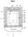
- Fig. 1 to Fig. 3 are explanatory diagram for explaining the first embodiment of the display device according to the present invention.
- Fig. 1 is a plan view schematically showing the display device.
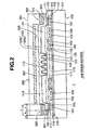
- Fig. 2 is a cross section schematically showing the cross section along direction A-B of Fig. 1 .
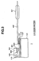
- Fig. 3 is a cross section schematically showing the cross section along direction C-D of Fig. 1 .
- the same reference numerals are given to the components corresponding in the respective diagrams.
- the display element area in the center of Fig. 2 is illustrated in a simplified manner.
- the display device 1 of the first embodiment shows a case of an organic EL display device.
- this display device 1 is structured from a TFT substrate 100 comprising a light emitting element array, a sealing substrate 200 for sealing the light emitting element array, a joining means 301 for joining the TFT substrate 100 and sealing substrate 200, a scan line driving unit 140 for driving the scan line of the TFT substrate 100, a data driver IC 401 for driving the data line of the TFT substrate 100, and so on.
- the TFT substrate 100 is structured from a plurality of organic EL light emitting elements 120 arranged in a matrix, a TFT transistor 130 for driving such light emitting elements 120 or which functions as a switch, and so on.
- a protective film 102 is formed on a glass substrate 101, silicon is deposited thereon, low-concentration impurities are injected therein and patterning is performed thereto in order to form a polysilicon TFT area 103.
- the substrate 100 may also be a resin substrate.
- a gate insulation film 104 formed of oxidized silicon is deposited thereon with the CVD method.
- Aluminum is deposited thereon with the sputtering method and patterning is performed thereto in order to form organic EL driving power source wiring films 105 and 106, an organic EL negative electrode wiring layer 107, and a gate wiring film 108 of the TFT 130.
- a mask is used to inject high-concentration ion into the source drain area of the TFT area 103, and oxidized silicon is deposited thereon in order to form a first interlayer insulation film 110.
- a contact hole mask is used to perform anisotropic etching in order to open a contact hole in the TFT area 103.
- aluminum is deposited thereon and pattering is performed thereto in order to from a source drain electrode 109 and a connection electrode 112.
- oxidized silicon is deposited thereon in order to form a second interlayer insulation film 111.
- the second interlayer insulation film for example, used may be an insulation film containing at least one element among boron, carbon, nitrogen, aluminum, silicon, phosphorus, ytterbium, samarium, erbium, yttrium, gadolinium, dysprosium, neodymium, and so on.
- a display element group described later is formed thereon.
- the center area of the TFT substrate 100 structured as described above is the display area to which the display element group is disposed.
- the light emitting element 120 of red emission, green emission and blue emission as the display element is arranged in a matrix with these three colors as a single pixel.
- Each of the emitted lights of the respective light emitting elements 120 is emitted outside via the glass substrate 101.
- light may also be abstracted from the side opposite the TFT substrate 100.
- the layers above the light emitting layer is structured of material having high optical transmittance.
- a bank layer 113 is form between the respective light emitting elements and at the periphery of the display area. This bank layer 113 may be formed, for instance, by patterning an organic material film such as a photoresist.
- the light emitting element 120 is structured from a transparent (ITO) positive electrode 121, an organic EL layer/electron hole transport layer 122, a negative electrode (common electrode) 123, and so on.
- the negative electrode 123 has a two-layer structure, and, for example, the lower layer is a calcium film 123a and the upper layer is an aluminum film 123b.
- the negative electrode 123a is-formed across the respective light emitting elements 120, the bank layers mutually between the respective light emitting elements 120, and the bank layer 113 at the periphery of the display area, and, the contact with the upper layer negative electrode 123b is secured thereby.
- the upper layer negative electrode 123b also functions as a wiring film, and is connected to the wiring film 107 in the area at the lower part of the sealing portion 202.
- the luminous efficiency can be improved by making the negative electrode 123a, which is in contact with the organic EL layer/electron hole transport layer 122, a calcium film, and, by covering the calcium film 123a in its entirety with the upper layer aluminum film 123b, low-resistance wiring and gas barrier (erosion prevention) are sought.
- this may also employ an organic EL element structure where an electron injection layer or an electron transport layer is additionally disposed on the light emitting layer (organic EL layer/electron hole transport layer), or a laminate of such electron injection layer and electron transport layer may be additionally disposed thereon.
- the top face of the substrate 100 structured as described above is sealed with a sealing substrate 200 having a cross inverted concave shape.
- This sealing substrate 200 is structured, for instance, from metal, glass, ceramic, plastic or the like, and comprises a tabular sealing plate 201, a protrusive sealing portion 202 formed around the periphery at the bottom face of this sealing plate, and a drying agent (material) 203.
- the drying agent 203 adsorbs the water vapor or oxygen gas infiltrating inside.
- Nitrogen gas as the inert gas is filled between the TFT substrate 100 and the-sealing substrate 200, and both substrates 100 and 200 are joined at the sealing portion 202 via an adhesive 301 as the joining means.
- the adhesive may be suitably selected from those having thermosetting properties or ultraviolet curing properties, in particular, those having low permeability against gas such as water vapor are employed.
- the substrate 100 is provided with a margin a for placing the sealing substrate 200.
- width d of the sealing portion 202 of the sealing substrate 200 is set to a suitable width (corresponds approximately to width b of the portion of only the adhesive 301 and the connection width c of the vertical wirings) for the adhesive 301 to prevent the infiltration of gas.
- this width width d of the adhesive 301 is made to be 1 mm or more so as to secure a long infiltration length of the outside atmosphere, whereby the infiltration of water vapor and oxygen gas from the adhesive layer will become difficult.
- the film thickness of the adhesive 301 is made to be 20 ⁇ m or less so as to reduce the contact face of the adhesive 301 and outside atmosphere, whereby the infiltration of gas will become difficult. This will also suppress the deterioration of elements sealed inside.
- the negative electrode film 123b is placed within the area at the lower part of this sealing portion 202 in an amount corresponding to the vertical connection width c, and connected to the wiring 107 of the substrate 100 via the ITO film 121and the source drain electrode film 112.
- the data line of the substrate 100 is connected to the electrode 121 of the substrate end, and connected to a wiring tape 402 via an anisotropic conductive film 303.
- the data driver IC 401 for driving the respective data lines is bonded in the middle of this wiring tape.
- a part of the negative electrode 123 is also placed into the sealing portion 202 at the lower part of the substrate 100.
- Fig. 4 shows a general joining example (comparative example) of the TFT substrate 100 and the sealing substrate 200.
- the components corresponding to those illustrated in Fig. 2 are given the same reference numerals, and the explanation of such components is omitted.
- a mounting margin a upon mounting the sealing substrate 200 on the TFT substrate 100 and a margin d of the adhesive 301 for preventing the infiltration of gas and securing reliability of sealing are secured outside the connection area c of the negative electrode 123 and the substrate wiring 107.
- the distance from the end of the TFT substrate 100 to the connection area c is mounting margin a + margin d of adhesive 301 + connection area c.
- the negative electrode 123 or the connection area c of the negative electrode 123 and the wiring 107 is placed into the lower part area (width d) of the sealing portion 202.
- the distance from the end of the TFT substrate 100 to the connection area is mounting margin a + margin d of adhesive 301.
- Margin d of the adhesive 301 will be approximately b+c, and the dimension of the non-display area will be reduced in an amount corresponding to the margin c of the wiring connection portion.
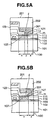
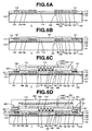
- the lower part area of the sealing portion 202 is formed, as shown in Fig. 5(a) , to be practically flat, or such that the unevenness does not change.
- Fig. 5(a) and Fig. 5(b) the components corresponding to those illustrated in Fig. 2 are given the same reference numerals, and the explanation of such components is omitted.
- x represents the connection width of the power source wiring 107 and the common electrode film 123
- y represents the misalignment between the power source wiring 107 and the common electrode film 123
- z represents the sealing margin under the sealing area at the periphery of the foregoing connection area.
- the power source wiring 107 of the TFT substrate 100 at the lower part area of the sealing portion 202 is formed to be relatively broad and flat.
- the power source wiring 107 is, as shown in Fig. 1 , disposed at the periphery of the substrate 100 so as not to intersect with other wirings. Thereby, the generation of unevenness arising from the intersecting of wirings is avoided as much as possible, and the power source wiring 107 is formed to be flat.
- the aluminum film 112 and iTO film 121 are formed flatly thereon and aluminum of the common electrode film 123 is further deposited on the flat face 1 of these conductive films in order to realize electrical connection with the negative electrode of the light emitting element 120.
- the top face (insulation film 111) m of the substrate 100 at the peripheral side of this connection area is also formed to be flat.
- the misalignment y between the power source wiring 107 and the common electrode film 123 is made to be 0.
- the width of the power source wiring 107 and the connection width of the common electrode 123 are coincided to minimize wiring resistance, and, as a result, the waste of measurement in the width direction can be avoided.
- the conductive portion (vertical conductive portion) x of the power source wiring film 107 and the common electrode 123 is formed to be flat, and the sealing area z of the periphery thereof is also made to be a flat area.
- Vertical conduction is carried out with certainty, unevenness of the film end portion after forming the common electrode film 123 is evenly formed, and height of the vertical conductive portion is aligned at the TFT substrate 100 side so as to prevent the sealing conditions from changing in the vertical conductive area portion.
- the stress applied to the sealing portion from can sealing can be made uniform.
- Fig. 6(a) to Fig. 6(d) are process charts for explaining the manufacturing process of the display device 1 according to the first embodiment.
- the TFT substrate 100 is formed.
- a silicon nitride film is deposited on the glass substrate 101 with the CVD method in order to form the protective film 102.
- Silicon is deposited thereon with the CVD method.
- low-concentration impurities are injected therein, and thermal processing of laser annealing is performed thereto in order to form the polysilicon film 103. Pattering is performed to this polysilicon film 103 in order to form the TFT area 130.
- the gate insulation film 104 formed from oxidized silicon is deposited thereon with the CVD method.
- Aluminum is deposited thereon with the sputtering method and patterning is performed thereto in order to form organic EL driving power source wiring films 105 and 106, the organic EL negative electrode wiring layer 107, and the gate wiring film 108 of the TFT 130.
- a mask is used to inject high-concentration ion into the source drain area of the TFT area 103, and the impurities are activated with thermal processing.
- oxidized silicon is deposited thereon with the CVD method in order to form the first interlayer insulation film 110.
- a contact hole mask is used to perform anisotropic etching to this interlayer insulation film 110 in order to open a contact hole in the source drain area of the TFT area 103.
- aluminum is deposited thereon and pattering is performed thereto in order to from the source drain electrode 109 and the connection electrode 112.
- oxidized silicon is deposited thereon in order to form the second interlayer insulation film 111.
- Etching is performed to the interlayer insulation film 111 on the wiring film 107 in order to expose the aluminum film 112.
- ITO is deposited thereon with the sputtering method, and pattering is performed thereto in order to form the positive electrode 121 of the light emitting element 120.
- the ITO film 121 is also deposited on the aluminum film 112 on the wiring film 107 in order to adjust the film thickness of the connection area and to prevent oxidization of the aluminum surface.
- a photosensitive organic resin film is applied with the spin coating method, and pattering is performed thereto in order to form the bank layer 113 in which the positive electrode (ITO) 121 of the light emitting element is exposed at the bottom part of the groove.
- This bank layer 113 separates the respective light emitting elements.
- the EL layer 122 is formed on the positive electrode 121 with the inkjet method.
- the EL layer 122 is structured, for example, from a light emitting layer, electron transport layer, electron injection layer, hole injection layer, hole transport layer, and so on.
- Calcium 123a for instance, is patterned on these light emitting elements 120 with vacuum deposition, and patterning is further performed thereto by evaporating the aluminum 123b.
- Calcium 123a and aluminum 123b structure the negative electrode (common electrode) 123 of the light emitting element 120.
- the aluminum film 123b is spread out to the periphery of the substrate 101 as the common electrode 123, and is connected to the wiring film 107 via the ITO film 121 and the aluminum film 112 at the margin c of the wiring connection portion (c.f. Fig. 2 ).
- an adhesive or sealant 301 is applied to the portion including the wiring film 107 at the periphery of the TFT substrate 100, and the sealing substrate 200 having an inverted concave shape with protrusions 202 at the periphery thereof is bonded under an inert gas atmosphere such as nitrogen gas.
- a drying agent is disposed inside the sealing substrate 200, and adsorbs the moisture or oxygen infiltrating inside.
- the adhesive preferably used is an insulation material that does not permeate oxygen or moisture, and photo-curing resin or thermosetting resin may be used.
- photo-curing resin or thermosetting resin may be used.
- epoxy resin or acrylate resin may be used.
- the display device is formed as described above.
- Fig. 7 and Fig. 8 The second example, not being part of the invention, is illustrated in Fig. 7 and Fig. 8 .
- the components corresponding to those illustrated in Fig. 2 and Fig. 3 are given the same reference numerals, and the explanation of such components is omitted.
- a flat substrate is used as the sealing substrate 200.
- the sealing substrate 200 preferably employed may be a glass plate, aluminum plate, stainless plate, acryl plate, ceramic plate, and so on.
- the adhesive 301 is used to fill the entire gap between the TFT substrate 100 and the sealing substrate 200 so as to join (bond) the two substrates. Even in this case also, the width of margins b+c necessary in securing the reliability of sealing described above including the connection area of the negative electrode 123 and the wiring film 107 of the substrate is secured, and the bank layer 113 is positioned to be inside the connection area of the negative electrode 123 and the wiring film 107 of the substrate. Thereby, the frame width can be narrowed, and, infiltration of gas into the bank layer 113 can be prevented as a result of placing the resin film 113, which has relatively high moisture permeability, away from the adhesive 301.
- Fig. 9(a) to Fig. 9(d) are process charts for explaining the manufacturing process of the display device 1 according to the second example, not being part of the invention.
- the components corresponding to those illustrated in Fig. 6 are given the same reference numerals, and the explanation of such components is omitted.
- the adhesive 301 is applied to the top face of the TFT substrate 100 with the spin coating method, inkjet method or transcription roller to achieve a suitable film thickness.
- the sealing substrate 200 is bonded on top of this adhesive film while being aligned with the TFT substrate 100.
- the adhesive 301 may also be applied to the sealing substrate 200 for bonding with the TFT substrate 100. Further, after aligning the sealing substrate 200 and the TFT substrate 100, an adhesive may be infiltrated inside from the peripheral gaps with the capillary phenomenon.
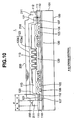
- Fig. 10 and Fig. 11 The third example, not being part of the invention is illustrated in Fig. 10 and Fig. 11 .
- the components corresponding to those illustrated in Fig. 2 and Fig. 3 are given the same reference numerals, and the explanation of such components is omitted.
- a multilayer thin film 210 is formed instead of the sealing substrate 200.
- Japanese Patent Laid-Open Publication No. 2000-223264 proposes a laminate film of an inorganic passivation sealing film and resin sealing film as the sealing film.
- the multilayer thin film 210 is formed on the TFT substrate 100, and covers the negative electrode 123 in its entirety.
- the multilayer thin film may adopt the various structures; for instance, the structure of an organic layer/inorganic layer/organic layer, or inorganic layer/organic layer/inorganic layer, and so on.
- the inorganic material for example, ceramic materials such as SiO 2 , SiN and SiON may be used, and, as the organic resin material, general hydrocarbon macromolecules such as polyethylene, polystyrene and polypropylene may be used. Moreover, this may also be fluoric macromolecules.
- the polymer materials themselves may be disposed, or precursors or monomers may be applied on the substrate for curing.
- the negative electrode 123 is connected to the power source wiring 107 at the end side of the substrate 100.
- the width of margins b+c necessary in securing the reliability of sealing described above including the connection area of the negative electrode 123 and the wiring film 107 of the substrate is secured, and the bank layer 113 is positioned to be inside the connection area of the negative electrode 123 and the wiring film 107 of the substrate. Thereby, the frame can be narrowed.
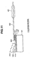
- Fig. 12(a) to Fig. 12(d) are process charts for explaining the manufacturing process of the display device 1 according to the third example, not being part of the invention
- the components corresponding to those illustrated in Fig. 6 are given the same reference numerals, and the explanation of such components is omitted.
- a highly airtight protective film 210 is used to cover the TFT substrate 100 so as to prevent the negative electrode 123 from being exposed to the outside air, and patterning is performed to the periphery thereof in order to enable separation of the substrate.
- the protective film 210 is preferably a multilayer thin film. As described above, the multilayer thin film may be formed by laminating an organic layer/inorganic layer/organic layer, or inorganic layer/organic layer/inorganic layer, and so on.
- the inorganic material for example, ceramic materials such as SiO 2 , SiN and SiON may be used, and, as the organic resin material, general hydrocarbon macromolecules such as polyethylene, polystyrene and polypropylene may be used. Moreover, this may also be fluoric macromolecules.
- the polymer materials themselves may be disposed, or precursors or monomers may be applied on the substrate for curing.
- Fig. 13 illustrates the second embodiment of the present invention.
- an example is illustrated where dummy pixels are further added to the display area of the display device of the foregoing first embodiment.
- Gas infiltrated inside the display device will penetrate within the film and affect the display area from the display elements on the peripheral side.
- influence of the infiltrated gas to the screen display is alleviated.
- the applied film can be formed evenly when a luminous material is applied with the inkjet method.
- minute ink (material) droplets are discharged from the nozzle, and, after the start of such discharge, time is required for the discharged rate to become stable.
- the coating film of the respective light emitting elements can be made uniform.
- the mask deposition method may also be employed instead of the inkjet method for forming the luminous body. Further, the inkjet method and mask deposition method may be used in combination.
- Fig. 14 to Fig. 17 illustrate yet other embodiments of the present invention.
- the components corresponding to those illustrated in Fig. 1 are given the same reference numerals, and the explanation of such components is omitted.
- the TFT substrate and the sealing substrate are placed together and sealed at the periphery of the substrates, one or more sides, or all of the sides of the periphery of the TFT substrate are narrowed.
- the power source wiring 107 and the common electrode (negative electrode) 123 are connected at the three sides (upper side, left side, right side) of the square (polygonal) substrate 100, narrowing of the frame is sought by sealing the outside areas thereof, and the driver IC (external circuit) is connected with the wiring tape 402 at one side (lower side).
- the driver IC external circuit
- wiring resistance can be reduced up to the common electrode 123 with the connection at three sides, and, since one side can be dedicated to connection with the external circuit, the frame of the overall display device module can be narrowed in a well-balanced manner.
- the power source wiring 107 and the common electrode (negative electrode) 123 are connected at one side (lower side) of the substrate 100, and sealing is performed at the outside area thereof.
- the common electrode 123 and the wiring film 107 are connected at only one side, it is difficult to narrow the frame since a sufficient conductive area (vertical conductive area) must be secured between the common electrode 123 and the wiring film 107 with this one side. Nevertheless, since the wiring with the common electrode 123 will no longer be necessary at the other three sides, the frame portion of such three sides can be narrowed significantly. This kind of structure is effective in cases as with a display device of a portable telephone wherein the module may be elongated in a certain direction, but is restricted in other directions.
- the common electrode 123 and the wiring film 107 are connected at two sides (left side and right side) of the substrate 100, and sealing is performed respectively to the outside areas thereof.
- this is effective when driving the odd number lines from the top and driving the even number lines from the bottom, and a large capacity (large screen) display is enabled by mounting numerous driver lCs.
- the reduction of wiring resistance comparable with the case of connecting the common electrode 123 and the wiring film 107 at three sides as depicted in Fig. 14 may be sought.
- the common electrode 123 and the wiring film 107 are connected at four sides (upper side, lower side, left side, right side) of the substrate 100, and sealing is performed respectively to the outside areas thereof. Then, a pullout wiring is formed via the insulation film at the lower part of the wiring for seeking conductivity between the common electrode 123 and the wiring film 107 with the multilayer wiring film, and this wiring is connected with an external circuit. Moreover, the conductive area for connecting the common electrode 123 and the wiring film 107 may be separated into a plurality of blocks, and a pullout wiring may be disposed between the mutual blocks. According to this kind of structure, sufficient reduction of wiring resistance required for realizing a large-size high resolution display can be attained.
- the frame area of the display unit can be reduced.
- the bank layer 113 is positioned to be further inside the substrate than the connection area (c) of the common electrode 123 and the substrate wiring 107, it is possible to prevent gas from directly penetrating within the bank layer 113 from the connection portion (b+c) of the substrate 100 and the sealing substrate (or sealing film) 200. Thereby, influence on the light emitting element 120 will be minimal even upon employing a resin (such as a photoresist), which can be processed easily, as the bank layer 113.
- a resin such as a photoresist
- Fig. 18 is a perspective view showing the structure of this personal computer.
- the personal computer 1100 is structured from a main body 1104 comprising a keyboard 1102, and a display device unit comprising the foregoing display device 1106.
- Fig. 19 is a perspective view showing the structure of this portable telephone.
- the portable telephone 1200 comprises a plurality of operation buttons 1202, an earpiece 1206,a mouthpiece 1204, and the foregoing display device 1208.
- Fig. 20 is a perspective view showing the structure of this digital still camera, and also briefly shows the connection with external equipment.
- the digital still camera 1300 generates image signals by performing photoelectric conversion to the optical image of the photographic subject with visual elements of a CCD (Charge Coupled Device) or the like.
- the foregoing display device 1304 is provided to the back face of the case 1302 of this digital still camera 1300, and is structured to conduct display based on the visual signals from the CCD.
- the display device 1304 functions as a finder for displaying the photographic subject.
- a light receiving unit including the likes of an optical lens or CCD is provided to the observation side of the case 1302.
- this digital still camera 1300 also comprises a video signal output terminal 1312 and a data transmission l/O terminal 1314 at the side face of the case 1302. And, as illustrated in Fig. 20 , a television monitor 1330 is connected to the video signal output terminal 1312 and a personal computer 1340 is connected to the data transmission I/O terminal 1314, respectively, as necessary. Further, pursuant to prescribed operations, the structure is such that the visual signal stored in the memory of the circuit substrate 1308 is output to the television monitor 1330 or the computer 1340.
- Fig. 21 is a perspective view showing the structure of an electronic book as an example of the electronic device according to the present invention.
- reference numeral 1400 represents the electronic book.
- the electronic book 1400 comprises a book-shaped frame 1402 and a cover 1403 capable of opening and closing this frame 1402.
- a display device 1404 is provided to the frame 1402 in a state where its display face is exposed to the surface thereof, and, an operation unit 1405 is also provided thereto.
- a controller, counter, memory and so on are built in the frame 1402.
- the display device 1404 comprises a pixel portion to which display elements are disposed and an integrated peripheral circuit that is provided integrally with such pixel portion.
- the peripheral circuit comprises a decoder scan driver and data driver.
- the electronic device in addition to the personal computer of Fig. 18 , the portable telephone of Fig. 19 , the digital still camera of Fig. 20 and the electronic book of Fig. 21 , electronic paper, liquid crystal televisions, view-finding or monitor-viewing video tape recorders, car navigation devices, pagers, electronic notebooks, calculators, word processors, workstations, television phones, OS terminals, devices comprising a touch panel and so on also apply.
- the foregoing display device may be employed as the display unit of the respective electronic devices described above.
- the display device according to the present invention is not limited to the organic EL display device of the embodiments.
- the substrate is not limited to the TFT substrate of the embodiments.
- the present invention can also be employed in a passive substrate.
- an adhesive was used as the joining means in the embodiments, it is not limited thereto. Other methods, for instance, joining with supersonic waves or lasers may also be employed.
- the width of the frame which is the non-display area at the periphery of the display area, can be narrowed.
Landscapes
- Engineering & Computer Science (AREA)
- Microelectronics & Electronic Packaging (AREA)
- Physics & Mathematics (AREA)
- Optics & Photonics (AREA)
- Chemical & Material Sciences (AREA)
- Inorganic Chemistry (AREA)
- Electroluminescent Light Sources (AREA)
- Devices For Indicating Variable Information By Combining Individual Elements (AREA)
Applications Claiming Priority (3)
| Application Number | Priority Date | Filing Date | Title |
|---|---|---|---|
| JP2002007337 | 2002-01-16 | ||
| JP2002007337 | 2002-01-16 | ||
| PCT/JP2003/000318 WO2003060858A1 (fr) | 2002-01-16 | 2003-01-16 | Dispositif d'affichage |
Publications (3)
| Publication Number | Publication Date |
|---|---|
| EP1450334A1 EP1450334A1 (en) | 2004-08-25 |
| EP1450334A4 EP1450334A4 (en) | 2007-11-21 |
| EP1450334B1 true EP1450334B1 (en) | 2012-08-01 |
Family
ID=19191321
Family Applications (1)
| Application Number | Title | Priority Date | Filing Date |
|---|---|---|---|
| EP03701742A Expired - Lifetime EP1450334B1 (en) | 2002-01-16 | 2003-01-16 | Display device |
Country Status (7)
| Country | Link |
|---|---|
| US (7) | US7038377B2 (ko) |
| EP (1) | EP1450334B1 (ko) |
| JP (9) | JP4251286B2 (ko) |
| KR (1) | KR100510421B1 (ko) |
| CN (1) | CN1253839C (ko) |
| TW (1) | TWI283142B (ko) |
| WO (1) | WO2003060858A1 (ko) |
Families Citing this family (122)
| Publication number | Priority date | Publication date | Assignee | Title |
|---|---|---|---|---|
| US7288420B1 (en) | 1999-06-04 | 2007-10-30 | Semiconductor Energy Laboratory Co., Ltd. | Method for manufacturing an electro-optical device |
| WO2003038749A1 (en) * | 2001-10-31 | 2003-05-08 | Icosystem Corporation | Method and system for implementing evolutionary algorithms |
| JP2003332045A (ja) * | 2002-05-09 | 2003-11-21 | Sanyo Electric Co Ltd | エレクトロルミネッセンス表示装置及びその製造方法 |
| JP3778176B2 (ja) * | 2002-05-28 | 2006-05-24 | セイコーエプソン株式会社 | 発光装置および電子機器 |
| JP2003347044A (ja) * | 2002-05-30 | 2003-12-05 | Sanyo Electric Co Ltd | 有機elパネル |
| US7449246B2 (en) * | 2004-06-30 | 2008-11-11 | General Electric Company | Barrier coatings |
| JP3906930B2 (ja) * | 2003-02-20 | 2007-04-18 | セイコーエプソン株式会社 | 電気光学装置及びその製造方法並びに電子機器 |
| JP3791618B2 (ja) | 2003-02-20 | 2006-06-28 | セイコーエプソン株式会社 | 電気光学装置及びその製造方法並びに電子機器 |
| JP3945525B2 (ja) * | 2003-02-20 | 2007-07-18 | セイコーエプソン株式会社 | 電気光学装置 |
| US7043463B2 (en) | 2003-04-04 | 2006-05-09 | Icosystem Corporation | Methods and systems for interactive evolutionary computing (IEC) |
| JP2005044613A (ja) * | 2003-07-28 | 2005-02-17 | Seiko Epson Corp | 発光装置の製造方法および発光装置 |
| KR100544123B1 (ko) * | 2003-07-29 | 2006-01-23 | 삼성에스디아이 주식회사 | 평판표시장치 |
| WO2005013081A2 (en) | 2003-08-01 | 2005-02-10 | Icosystem Corporation | Methods and systems for applying genetic operators to determine system conditions |
| JP3915985B2 (ja) * | 2003-08-22 | 2007-05-16 | セイコーエプソン株式会社 | 画素素子基板、表示装置、電子機器、及び画素素子基板の製造方法 |
| US7356518B2 (en) * | 2003-08-27 | 2008-04-08 | Icosystem Corporation | Methods and systems for multi-participant interactive evolutionary computing |
| KR100552972B1 (ko) | 2003-10-09 | 2006-02-15 | 삼성에스디아이 주식회사 | 평판표시장치 및 그의 제조방법 |
| JP4678124B2 (ja) * | 2003-11-10 | 2011-04-27 | セイコーエプソン株式会社 | 電気光学装置、電気光学装置の製造方法及び電子機器 |
| WO2005047967A1 (en) * | 2003-11-14 | 2005-05-26 | Semiconductor Energy Laboratory Co., Ltd. | Liquid crystal display device and method for manufacturing the same |
| KR101111470B1 (ko) * | 2003-11-14 | 2012-02-21 | 가부시키가이샤 한도오따이 에네루기 켄큐쇼 | 표시 장치 및 그 제조 방법 |
| KR100600865B1 (ko) | 2003-11-19 | 2006-07-14 | 삼성에스디아이 주식회사 | 전자파차폐수단을 포함하는 능동소자표시장치 |
| KR100611153B1 (ko) | 2003-11-27 | 2006-08-09 | 삼성에스디아이 주식회사 | 평판 표시 소자 |
| JP4899286B2 (ja) * | 2004-01-30 | 2012-03-21 | セイコーエプソン株式会社 | 有機el表示装置及びその製造方法、並びに電子機器 |
| JP4058695B2 (ja) * | 2004-02-16 | 2008-03-12 | セイコーエプソン株式会社 | 電気光学装置及び電子機器 |
| KR100615212B1 (ko) | 2004-03-08 | 2006-08-25 | 삼성에스디아이 주식회사 | 평판 표시 장치 |
| KR100581903B1 (ko) | 2004-03-09 | 2006-05-22 | 삼성에스디아이 주식회사 | 전계 발광 디스플레이 장치 |
| US7619258B2 (en) * | 2004-03-16 | 2009-11-17 | Semiconductor Energy Laboratory Co., Ltd. | Display device |
| US7764012B2 (en) * | 2004-04-16 | 2010-07-27 | Semiconductor Energy Laboratory Co., Ltd | Light emitting device comprising reduced frame portion, manufacturing method with improve productivity thereof, and electronic apparatus |
| EP1782285A1 (en) * | 2004-07-06 | 2007-05-09 | Icosystem Corporation | Methods and apparatus for query refinement using genetic algorithms |
| US7707220B2 (en) * | 2004-07-06 | 2010-04-27 | Icosystem Corporation | Methods and apparatus for interactive searching techniques |
| KR100698689B1 (ko) * | 2004-08-30 | 2007-03-23 | 삼성에스디아이 주식회사 | 발광 표시장치와 그의 제조방법 |
| US7527994B2 (en) * | 2004-09-01 | 2009-05-05 | Honeywell International Inc. | Amorphous silicon thin-film transistors and methods of making the same |
| US8350466B2 (en) | 2004-09-17 | 2013-01-08 | Semiconductor Energy Laboratory Co., Ltd. | Display device and manufacturing method thereof |
| ATE541327T1 (de) * | 2004-10-21 | 2012-01-15 | Lg Display Co Ltd | Organische elektrolumineszente vorrichtung und herstellungsverfahren |
| TWI411349B (zh) * | 2004-11-19 | 2013-10-01 | Semiconductor Energy Lab | 顯示裝置及電子裝置 |
| EP1724853B1 (en) * | 2005-05-17 | 2015-05-06 | LG Display Co., Ltd. | Organic electroluminescent device |
| EP1760798B1 (en) * | 2005-08-31 | 2012-01-11 | Semiconductor Energy Laboratory Co., Ltd. | Semiconductor device and manufacturing method thereof |
| EP1760776B1 (en) * | 2005-08-31 | 2019-12-25 | Semiconductor Energy Laboratory Co., Ltd. | Manufacturing method for semiconductor device with flexible substrate |
| WO2007035848A2 (en) * | 2005-09-21 | 2007-03-29 | Icosystem Corporation | System and method for aiding product design and quantifying acceptance |
| JP2007123240A (ja) | 2005-09-28 | 2007-05-17 | Sony Corp | 表示装置の製造方法および表示装置 |
| JP4827499B2 (ja) * | 2005-11-16 | 2011-11-30 | キヤノン株式会社 | 電流駆動型装置及び表示装置 |
| US7851996B2 (en) * | 2005-11-16 | 2010-12-14 | Canon Kabushiki Kaisha | Display apparatus |
| JP4736757B2 (ja) * | 2005-12-01 | 2011-07-27 | セイコーエプソン株式会社 | 発光装置および電子機器 |
| JP4742835B2 (ja) * | 2005-12-05 | 2011-08-10 | セイコーエプソン株式会社 | 発光装置および電子機器 |
| KR100673765B1 (ko) | 2006-01-20 | 2007-01-24 | 삼성에스디아이 주식회사 | 유기전계발광 표시장치 및 그 제조방법 |
| US8038495B2 (en) | 2006-01-20 | 2011-10-18 | Samsung Mobile Display Co., Ltd. | Organic light-emitting display device and manufacturing method of the same |
| KR100635514B1 (ko) | 2006-01-23 | 2006-10-18 | 삼성에스디아이 주식회사 | 유기전계발광표시장치 및 그 제조방법 |
| KR100671647B1 (ko) | 2006-01-26 | 2007-01-19 | 삼성에스디아이 주식회사 | 유기전계발광 표시 장치 |
| KR100688792B1 (ko) * | 2006-01-27 | 2007-03-02 | 삼성에스디아이 주식회사 | 평판 표시장치 및 그의 제조방법 |
| KR100759666B1 (ko) * | 2006-01-27 | 2007-09-17 | 삼성에스디아이 주식회사 | 평판 표시장치 및 그의 제조방법 |
| JP5160754B2 (ja) * | 2006-01-31 | 2013-03-13 | エルジー ディスプレイ カンパニー リミテッド | El装置 |
| JP4533392B2 (ja) * | 2006-03-22 | 2010-09-01 | キヤノン株式会社 | 有機発光装置 |
| JP4736890B2 (ja) * | 2006-03-28 | 2011-07-27 | 大日本印刷株式会社 | 有機エレクトロルミネッセンス素子 |
| JP4864520B2 (ja) * | 2006-04-12 | 2012-02-01 | 三菱電機株式会社 | 有機el表示装置および有機el表示装置の製造方法 |
| KR100914784B1 (ko) * | 2006-05-17 | 2009-08-31 | 엘지디스플레이 주식회사 | 전계발광소자 및 그 제조방법 |
| EP2027760A2 (en) * | 2006-05-22 | 2009-02-25 | Philips Intellectual Property & Standards GmbH | Interconnection arrangement and method for interconnecting a high-cuurent carrying cable with a metal thin-film |
| KR101281888B1 (ko) * | 2006-06-30 | 2013-07-03 | 엘지디스플레이 주식회사 | 유기 전계 발광 표시 장치 및 이의 제조 방법 |
| JP2008047340A (ja) * | 2006-08-11 | 2008-02-28 | Dainippon Printing Co Ltd | 有機エレクトロルミネッセンス素子 |
| JP4245032B2 (ja) * | 2006-10-03 | 2009-03-25 | セイコーエプソン株式会社 | 発光装置および電子機器 |
| US7792816B2 (en) * | 2007-02-01 | 2010-09-07 | Icosystem Corporation | Method and system for fast, generic, online and offline, multi-source text analysis and visualization |
| KR100830981B1 (ko) * | 2007-04-13 | 2008-05-20 | 삼성에스디아이 주식회사 | 유기 발광 표시 장치 |
| JP2008311059A (ja) | 2007-06-14 | 2008-12-25 | Rohm Co Ltd | 有機エレクトロルミネセンス素子及びその製造方法 |
| JP5208591B2 (ja) * | 2007-06-28 | 2013-06-12 | 株式会社半導体エネルギー研究所 | 発光装置、及び照明装置 |
| JP4884320B2 (ja) * | 2007-06-29 | 2012-02-29 | 京セラ株式会社 | 画像表示装置 |
| TW200915820A (en) * | 2007-09-19 | 2009-04-01 | Giga Byte Tech Co Ltd | Touch panel structure having dual touch-modes, and signal processing method and device |
| JP5119865B2 (ja) * | 2007-11-02 | 2013-01-16 | セイコーエプソン株式会社 | 有機エレクトロルミネッセンス装置、電子機器 |
| KR101362164B1 (ko) * | 2007-12-11 | 2014-02-12 | 엘지디스플레이 주식회사 | 유기 전계 발광 표시 장치 및 그 제조 방법 |
| JP5163430B2 (ja) * | 2008-01-09 | 2013-03-13 | セイコーエプソン株式会社 | 電気光学装置および電子機器 |
| WO2009110136A1 (ja) * | 2008-03-04 | 2009-09-11 | シャープ株式会社 | 表示装置用基板、その製造方法、表示装置、多層配線の形成方法及び多層配線基板 |
| WO2010032329A1 (ja) * | 2008-09-22 | 2010-03-25 | パイオニア株式会社 | El発光装置 |
| KR101938125B1 (ko) * | 2008-12-17 | 2019-01-15 | 가부시키가이샤 한도오따이 에네루기 켄큐쇼 | 발광 장치 및 전자 기기 |
| JP2010170776A (ja) * | 2009-01-21 | 2010-08-05 | Konica Minolta Holdings Inc | 有機エレクトロニクス素子およびその製造方法 |
| JP5190709B2 (ja) * | 2009-02-20 | 2013-04-24 | カシオ計算機株式会社 | 表示パネル及びその製造方法 |
| KR20110019498A (ko) * | 2009-08-20 | 2011-02-28 | 삼성모바일디스플레이주식회사 | 유기전계발광 표시장치 |
| JP5218460B2 (ja) * | 2010-03-26 | 2013-06-26 | セイコーエプソン株式会社 | 焦電型光検出器、焦電型光検出装置及び電子機器 |
| JP5471774B2 (ja) | 2010-04-27 | 2014-04-16 | セイコーエプソン株式会社 | 電気光学装置、電気光学装置の製造方法、電子機器 |
| KR101845480B1 (ko) * | 2010-06-25 | 2018-04-04 | 가부시키가이샤 한도오따이 에네루기 켄큐쇼 | 반도체 장치의 제작 방법 |
| KR101201720B1 (ko) * | 2010-07-29 | 2012-11-15 | 삼성디스플레이 주식회사 | 표시 장치 및 유기 발광 표시 장치 |
| DE102010032834B4 (de) * | 2010-07-30 | 2023-05-25 | Pictiva Displays International Limited | Optoelektronische Vorrichtung und Verfahren zu deren Herstellung |
| KR20120028418A (ko) * | 2010-09-14 | 2012-03-23 | 삼성모바일디스플레이주식회사 | 유기 발광 표시 장치용 밀봉기판의 제조 방법 및 유기 발광 표시 장치용 밀봉기판 |
| JP5003808B2 (ja) * | 2010-09-17 | 2012-08-15 | セイコーエプソン株式会社 | 電気光学装置および電子機器 |
| KR101757810B1 (ko) * | 2010-11-19 | 2017-07-17 | 삼성디스플레이 주식회사 | 표시 장치, 유기 발광 표시 장치, 및 밀봉 기판의 제조 방법 |
| KR20120089108A (ko) * | 2011-02-01 | 2012-08-09 | 삼성전기주식회사 | 터치패널 |
| US8823659B2 (en) | 2011-06-07 | 2014-09-02 | Nokia Corporation | Method and apparatus for touch panel |
| KR20120138168A (ko) * | 2011-06-14 | 2012-12-24 | 삼성디스플레이 주식회사 | 표시 장치 및 표시 장치 제조 방법 |
| WO2013008765A1 (en) | 2011-07-08 | 2013-01-17 | Semiconductor Energy Laboratory Co., Ltd. | Light-emitting module, light-emitting device, and method for manufacturing the light-emitting module |
| CN103085437B (zh) * | 2011-11-02 | 2016-04-06 | 宸鸿科技(厦门)有限公司 | 贴合结构、具有该贴合结构之电子装置及其贴合方法 |
| JP5318182B2 (ja) * | 2011-11-30 | 2013-10-16 | キヤノン株式会社 | 有機el素子の製造方法 |
| JP2013235128A (ja) * | 2012-05-09 | 2013-11-21 | Seiko Epson Corp | 電気光学装置の製造方法、及び電気光学装置用基板 |
| CN102800815B (zh) * | 2012-08-06 | 2015-05-20 | 深圳市华星光电技术有限公司 | 有机显示装置及其制作方法 |
| TWI559064B (zh) | 2012-10-19 | 2016-11-21 | Japan Display Inc | Display device |
| JP6228735B2 (ja) * | 2013-02-21 | 2017-11-08 | 株式会社ジャパンディスプレイ | 表示装置 |
| KR101960388B1 (ko) * | 2012-12-24 | 2019-03-20 | 엘지디스플레이 주식회사 | 유기 발광 다이오드 표시 장치 |
| KR101980766B1 (ko) * | 2012-12-27 | 2019-05-21 | 엘지디스플레이 주식회사 | 터치 패널 내장형 유기 발광 다이오드 표시 장치 |
| JP6221386B2 (ja) | 2013-06-18 | 2017-11-01 | セイコーエプソン株式会社 | 発光装置および電子機器 |
| JP6217161B2 (ja) * | 2013-06-19 | 2017-10-25 | セイコーエプソン株式会社 | 発光装置および電子機器 |
| KR102079257B1 (ko) | 2013-06-28 | 2020-02-20 | 삼성디스플레이 주식회사 | 박막 트랜지스터 어레이 기판 및 이를 포함하는 유기발광표시장치 |
| KR20150011231A (ko) * | 2013-07-22 | 2015-01-30 | 삼성디스플레이 주식회사 | 유기 발광 표시 장치 및 이의 제조 방법 |
| KR20150021000A (ko) * | 2013-08-19 | 2015-02-27 | 가부시키가이샤 한도오따이 에네루기 켄큐쇼 | 표시 장치 |
| KR102117612B1 (ko) | 2013-08-28 | 2020-06-02 | 삼성디스플레이 주식회사 | 유기 발광 표시 장치 및 이의 제조 방법 |
| JP5981904B2 (ja) * | 2013-11-15 | 2016-08-31 | 株式会社ナンシン | キャスタの取付構造 |
| CN111081734A (zh) * | 2014-03-17 | 2020-04-28 | 松下电器产业株式会社 | 薄膜晶体管元件基板及其制造方法、和有机el显示装置 |
| CN104216159B (zh) * | 2014-09-03 | 2017-09-22 | 上海天马有机发光显示技术有限公司 | 一种显示面板及其制备方法、显示装置 |
| TWI552334B (zh) * | 2015-03-25 | 2016-10-01 | 友達光電股份有限公司 | 顯示面板之畫素結構 |
| KR102442616B1 (ko) * | 2015-04-08 | 2022-09-14 | 삼성디스플레이 주식회사 | 유기 발광 표시 장치 및 그 제조 방법 |
| US20180173032A1 (en) * | 2015-06-16 | 2018-06-21 | Sharp Kabushiki Kaisha | Method of producing display device, and display device |
| JP2017037172A (ja) * | 2015-08-10 | 2017-02-16 | 株式会社ジャパンディスプレイ | 表示装置 |
| KR102554963B1 (ko) * | 2015-10-29 | 2023-07-11 | 엘지디스플레이 주식회사 | 유기 발광 표시 장치 |
| KR102502656B1 (ko) * | 2015-12-15 | 2023-02-21 | 엘지디스플레이 주식회사 | 유기 발광 표시 장치 |
| JP6557601B2 (ja) | 2015-12-29 | 2019-08-07 | 株式会社ジャパンディスプレイ | 表示装置、表示装置の製造方法 |
| KR102605957B1 (ko) * | 2016-02-23 | 2023-11-27 | 삼성디스플레이 주식회사 | 유기 발광 표시 장치 및 유기 발광 표시 장치의 제조 방법 |
| JP6714401B2 (ja) * | 2016-03-18 | 2020-06-24 | 株式会社ジャパンディスプレイ | 表示装置 |
| CN106293252B (zh) * | 2016-09-09 | 2020-02-07 | 上海中航光电子有限公司 | 阵列基板及显示装置 |
| WO2018179308A1 (ja) * | 2017-03-31 | 2018-10-04 | シャープ株式会社 | 表示装置およびその製造方法 |
| JP6912080B2 (ja) * | 2017-06-09 | 2021-07-28 | 株式会社Joled | 有機el表示パネル |
| WO2019130427A1 (ja) * | 2017-12-26 | 2019-07-04 | シャープ株式会社 | 表示デバイス |
| KR102546170B1 (ko) * | 2018-01-19 | 2023-06-22 | 삼성디스플레이 주식회사 | 표시 장치 |
| JP2019153551A (ja) * | 2018-03-06 | 2019-09-12 | 株式会社ジャパンディスプレイ | 有機el表示装置 |
| CN111903187B (zh) | 2018-03-28 | 2023-07-04 | 夏普株式会社 | 显示装置 |
| US10804491B2 (en) * | 2018-12-13 | 2020-10-13 | Wuhan China Star Optoelectronics Semiconductor Display Technology Co., Ltd. | Organic light emitting diode display device |
| RU2729699C1 (ru) | 2019-08-01 | 2020-08-11 | Боэ Текнолоджи Груп Ко., Лтд. | Подложка отображения и устройство отображения |
| JP7418077B2 (ja) * | 2019-08-30 | 2024-01-19 | キヤノン株式会社 | 半導体装置、表示装置、及び電子機器 |
| KR20220092098A (ko) | 2020-12-24 | 2022-07-01 | 엘지디스플레이 주식회사 | 표시장치 |
Family Cites Families (69)
| Publication number | Priority date | Publication date | Assignee | Title |
|---|---|---|---|---|
| JPH0752668B2 (ja) * | 1988-11-16 | 1995-06-05 | シャープ株式会社 | 薄膜el素子 |
| JPH04278983A (ja) | 1991-03-07 | 1992-10-05 | Fuji Electric Co Ltd | 表示パネルの封止方法 |
| KR100228520B1 (ko) * | 1992-08-13 | 1999-11-01 | 가시오 가즈오 | 박막트렌지스터 어레이 및 박막트렌지스터 어레이를 이용한 액정표시장치 |
| US5504390A (en) * | 1994-03-03 | 1996-04-02 | Topp; Mark | Addressable electroluminescent display panel having a continuous footprint |
| US6025901A (en) * | 1995-08-14 | 2000-02-15 | Sharp Kabushiki Kaisha | Liquid crystal display device and method for producing the same |
| JPH0982476A (ja) * | 1995-09-14 | 1997-03-28 | Casio Comput Co Ltd | 有機電界発光素子 |
| JPH09148066A (ja) * | 1995-11-24 | 1997-06-06 | Pioneer Electron Corp | 有機el素子 |
| JPH1048654A (ja) * | 1996-07-30 | 1998-02-20 | Nec Kagoshima Ltd | Lcdパネルの端子構造 |
| JP4354019B2 (ja) * | 1997-04-18 | 2009-10-28 | 出光興産株式会社 | 有機エレクトロルミネッセンス素子 |
| JPH10198285A (ja) * | 1997-01-13 | 1998-07-31 | Toshiba Corp | 平面表示装置 |
| KR100260611B1 (ko) * | 1997-04-03 | 2000-07-01 | 윤종용 | 배선을 수리하기 위한 평판 표시 장치용 기판 |
| US6147724A (en) * | 1997-04-04 | 2000-11-14 | Hitachi, Ltd. | Back light system for minimizing non display area of liquid crystal display device |
| JP3541625B2 (ja) * | 1997-07-02 | 2004-07-14 | セイコーエプソン株式会社 | 表示装置及びアクティブマトリクス基板 |
| JP3580092B2 (ja) * | 1997-08-21 | 2004-10-20 | セイコーエプソン株式会社 | アクティブマトリクス型表示装置 |
| JP3830238B2 (ja) | 1997-08-29 | 2006-10-04 | セイコーエプソン株式会社 | アクティブマトリクス型装置 |
| KR100249784B1 (ko) * | 1997-11-20 | 2000-04-01 | 정선종 | 고분자복합막을이용한유기물혹은고분자전기발광소자의패키징방법 |
| JP2000003783A (ja) * | 1998-06-12 | 2000-01-07 | Tdk Corp | 有機el表示装置 |
| JP2000173766A (ja) * | 1998-09-30 | 2000-06-23 | Sanyo Electric Co Ltd | 表示装置 |
| JP3423232B2 (ja) * | 1998-11-30 | 2003-07-07 | 三洋電機株式会社 | アクティブ型el表示装置 |
| JP2000174282A (ja) * | 1998-12-03 | 2000-06-23 | Semiconductor Energy Lab Co Ltd | 半導体装置 |
| JP3817081B2 (ja) | 1999-01-29 | 2006-08-30 | パイオニア株式会社 | 有機el素子の製造方法 |
| JP3549760B2 (ja) * | 1999-02-18 | 2004-08-04 | シャープ株式会社 | 平面型表示装置 |
| JP3670923B2 (ja) * | 1999-02-26 | 2005-07-13 | 三洋電機株式会社 | カラー有機el表示装置 |
| EP1186065A1 (en) * | 1999-04-28 | 2002-03-13 | E.I. Du Pont De Nemours And Company | Flexible organic electronic device with improved resistance to oxygen and moisture degradation |
| JP2000315058A (ja) * | 1999-04-30 | 2000-11-14 | Toshiba Corp | 表示装置用アレイ基板 |
| JP4075028B2 (ja) * | 1999-06-14 | 2008-04-16 | セイコーエプソン株式会社 | 回路基板、表示装置、および電子機器 |
| JP2001078463A (ja) * | 1999-09-06 | 2001-03-23 | Amada Co Ltd | 主スイッチ過電流保護回路を備えた高周波インバータ |
| CN1186683C (zh) | 1999-09-08 | 2005-01-26 | 松下电器产业株式会社 | 显示装置及其制造方法 |
| JP2001154218A (ja) * | 1999-09-08 | 2001-06-08 | Matsushita Electric Ind Co Ltd | 表示装置およびその製造方法 |
| US6833668B1 (en) | 1999-09-29 | 2004-12-21 | Sanyo Electric Co., Ltd. | Electroluminescence display device having a desiccant |
| US6876145B1 (en) * | 1999-09-30 | 2005-04-05 | Semiconductor Energy Laboratory Co., Ltd. | Organic electroluminescent display device |
| JP2001109395A (ja) * | 1999-10-01 | 2001-04-20 | Sanyo Electric Co Ltd | El表示装置 |
| JP2001102169A (ja) | 1999-10-01 | 2001-04-13 | Sanyo Electric Co Ltd | El表示装置 |
| JP2001109398A (ja) * | 1999-10-04 | 2001-04-20 | Sanyo Electric Co Ltd | 表示装置 |
| US6623861B2 (en) * | 2001-04-16 | 2003-09-23 | Battelle Memorial Institute | Multilayer plastic substrates |
| JP2001125509A (ja) * | 1999-10-28 | 2001-05-11 | Nippon Seiki Co Ltd | 電界発光表示素子 |
| JP4823413B2 (ja) * | 1999-10-29 | 2011-11-24 | 株式会社半導体エネルギー研究所 | 自発光装置 |
| TW478019B (en) | 1999-10-29 | 2002-03-01 | Semiconductor Energy Lab | Self light-emitting device |
| US8957584B2 (en) | 1999-10-29 | 2015-02-17 | Semiconductor Energy Laboratory Co., Ltd. | Self light-emitting device |
| TW525122B (en) * | 1999-11-29 | 2003-03-21 | Semiconductor Energy Lab | Electronic device |
| JP4727029B2 (ja) * | 1999-11-29 | 2011-07-20 | 株式会社半導体エネルギー研究所 | El表示装置、電気器具及びel表示装置用の半導体素子基板 |
| JP2001189190A (ja) | 2000-01-06 | 2001-07-10 | Auto Network Gijutsu Kenkyusho:Kk | 有機el表示装置 |
| TW480727B (en) * | 2000-01-11 | 2002-03-21 | Semiconductor Energy Laboratro | Semiconductor display device |
| JP2001195026A (ja) * | 2000-01-14 | 2001-07-19 | Victor Co Of Japan Ltd | マトリクス型表示装置 |
| US6633121B2 (en) * | 2000-01-31 | 2003-10-14 | Idemitsu Kosan Co., Ltd. | Organic electroluminescence display device and method of manufacturing same |
| JP3495305B2 (ja) * | 2000-02-02 | 2004-02-09 | Necエレクトロニクス株式会社 | 半導体装置及び半導体モジュール |
| JP2001222237A (ja) * | 2000-02-07 | 2001-08-17 | Kyocera Corp | 表示装置およびその製造方法 |
| JP2001318627A (ja) * | 2000-02-29 | 2001-11-16 | Semiconductor Energy Lab Co Ltd | 発光装置 |
| JP4637391B2 (ja) * | 2000-03-27 | 2011-02-23 | 株式会社半導体エネルギー研究所 | 発光装置の作製方法 |
| JP2001272930A (ja) * | 2000-03-28 | 2001-10-05 | Sanyo Electric Co Ltd | エレクトロルミネッセンス表示装置 |
| US6706544B2 (en) * | 2000-04-19 | 2004-03-16 | Semiconductor Energy Laboratory Co., Ltd. | Light emitting device and fabricating method thereof |
| TW536836B (en) * | 2000-05-22 | 2003-06-11 | Semiconductor Energy Lab | Light emitting device and electrical appliance |
| JP4831889B2 (ja) * | 2000-06-22 | 2011-12-07 | 株式会社半導体エネルギー研究所 | 表示装置 |
| US7019718B2 (en) * | 2000-07-25 | 2006-03-28 | Semiconductor Energy Laboratory Co., Ltd. | Display device |
| US6605826B2 (en) * | 2000-08-18 | 2003-08-12 | Semiconductor Energy Laboratory Co., Ltd. | Light-emitting device and display device |
| JP2002110344A (ja) * | 2000-09-29 | 2002-04-12 | Tdk Corp | 薄膜el素子及びその製造方法 |
| US6900590B2 (en) * | 2000-10-17 | 2005-05-31 | Samsung Sdi Co., Ltd. | Organic electroluminescent device having non-continuous metal auxiliary electrodes |
| JP2002141171A (ja) * | 2000-10-31 | 2002-05-17 | Nippon Seiki Co Ltd | 表示装置 |
| JP4011337B2 (ja) * | 2000-12-12 | 2007-11-21 | 株式会社半導体エネルギー研究所 | 発光装置及びその作製方法。 |
| TWI255817B (en) | 2001-02-14 | 2006-06-01 | Kissei Pharmaceutical | Glucopyranosyloxybenzylbenzene derivatives and medicinal use thereof |
| TW548860B (en) * | 2001-06-20 | 2003-08-21 | Semiconductor Energy Lab | Light emitting device and method of manufacturing the same |
| TW519853B (en) * | 2001-10-17 | 2003-02-01 | Chi Mei Electronic Corp | Organic electro-luminescent display and its packaging method |
| US6888305B2 (en) * | 2001-11-06 | 2005-05-03 | Universal Display Corporation | Encapsulation structure that acts as a multilayer mirror |
| US6597111B2 (en) * | 2001-11-27 | 2003-07-22 | Universal Display Corporation | Protected organic optoelectronic devices |
| JP3823916B2 (ja) * | 2001-12-18 | 2006-09-20 | セイコーエプソン株式会社 | 表示装置及び電子機器並びに表示装置の製造方法 |
| JP4101511B2 (ja) * | 2001-12-27 | 2008-06-18 | 株式会社半導体エネルギー研究所 | 発光装置及びその作製方法 |
| JP2003208976A (ja) * | 2002-01-11 | 2003-07-25 | Seiko Epson Corp | エレクトロルミネッセンス装置及びその製造方法、並びに電子機器 |
| US6810919B2 (en) * | 2002-01-11 | 2004-11-02 | Seiko Epson Corporation | Manufacturing method for display device, display device, manufacturing method for electronic apparatus, and electronic apparatus |
| KR100858936B1 (ko) * | 2007-07-12 | 2008-09-18 | 경성대학교 산학협력단 | 양이온 함유 수용성 고분자층을 포함하는 고분자 유기 전계발광 소자 및 그 제조방법 |
-
2003
- 2003-01-14 US US10/341,392 patent/US7038377B2/en not_active Expired - Lifetime
- 2003-01-16 CN CNB03800061XA patent/CN1253839C/zh not_active Expired - Lifetime
- 2003-01-16 WO PCT/JP2003/000318 patent/WO2003060858A1/ja active Application Filing
- 2003-01-16 EP EP03701742A patent/EP1450334B1/en not_active Expired - Lifetime
- 2003-01-16 JP JP2003560880A patent/JP4251286B2/ja not_active Expired - Lifetime
- 2003-01-16 KR KR10-2003-7012715A patent/KR100510421B1/ko active IP Right Grant
- 2003-01-16 TW TW092100891A patent/TWI283142B/zh not_active IP Right Cessation
-
2005
- 2005-01-03 US US11/025,948 patent/US7190116B2/en not_active Ceased
- 2005-06-22 JP JP2005181578A patent/JP4701858B2/ja not_active Expired - Lifetime
- 2005-06-22 JP JP2005181577A patent/JP4254752B2/ja not_active Expired - Lifetime
-
2008
- 2008-06-23 JP JP2008162863A patent/JP5245566B2/ja not_active Expired - Lifetime
- 2008-06-25 JP JP2008165626A patent/JP4983734B2/ja not_active Expired - Lifetime
- 2008-10-02 JP JP2008257149A patent/JP4983766B2/ja not_active Expired - Lifetime
-
2009
- 2009-02-19 JP JP2009036206A patent/JP4983821B2/ja not_active Expired - Lifetime
- 2009-03-13 US US12/404,057 patent/USRE42215E1/en not_active Expired - Lifetime
-
2011
- 2011-02-03 US US13/020,533 patent/USRE43738E1/en not_active Expired - Lifetime
- 2011-06-02 JP JP2011124164A patent/JP5299475B2/ja not_active Expired - Lifetime
-
2012
- 2012-07-10 US US13/545,596 patent/USRE44902E1/en not_active Expired - Lifetime
-
2013
- 2013-01-15 JP JP2013004326A patent/JP5392424B2/ja not_active Expired - Lifetime
- 2013-06-21 US US13/923,911 patent/USRE45556E1/en not_active Expired - Lifetime
-
2015
- 2015-04-30 US US14/700,798 patent/USRE47817E1/en not_active Expired - Lifetime
Also Published As
Similar Documents
| Publication | Publication Date | Title |
|---|---|---|
| EP1450334B1 (en) | Display device | |
| KR102668295B1 (ko) | 표시 장치 | |
| US6686063B2 (en) | Organic electroluminescent device, method for manufacturing organic electroluminescent device, and electronic apparatus | |
| EP3488478B1 (en) | Method of fabricating display panel | |
| CN108417602B (zh) | 有机el装置的制造方法、有机el装置、电子设备 | |
| KR20020009498A (ko) | 표시장치 | |
| JP2010027504A (ja) | 有機el装置及び電子機器 | |
| JP4952318B2 (ja) | エレクトロルミネッセンス装置の製造方法 | |
| JP2008153043A (ja) | エレクトロルミネッセンス装置及び電子機器 | |
| CN220755384U (zh) | 显示面板及显示装置 | |
| CN117918041A (zh) | 显示面板及其制造方法、显示装置 |
Legal Events
| Date | Code | Title | Description |
|---|---|---|---|
| PUAI | Public reference made under article 153(3) epc to a published international application that has entered the european phase |
Free format text: ORIGINAL CODE: 0009012 |
|
| 17P | Request for examination filed |
Effective date: 20040102 |
|
| AK | Designated contracting states |
Kind code of ref document: A1 Designated state(s): AT BE BG CH CY CZ DE DK EE ES FI FR GB GR IE IT LI LU MC NL PT SE SI SK TR |
|
| A4 | Supplementary search report drawn up and despatched |
Effective date: 20071019 |
|
| 17Q | First examination report despatched |
Effective date: 20080404 |
|
| REG | Reference to a national code |
Ref country code: DE Ref legal event code: R079 Ref document number: 60341649 Country of ref document: DE Free format text: PREVIOUS MAIN CLASS: G09F0009300000 Ipc: H01L0027320000 |
|
| GRAP | Despatch of communication of intention to grant a patent |
Free format text: ORIGINAL CODE: EPIDOSNIGR1 |
|
| RIC1 | Information provided on ipc code assigned before grant |
Ipc: H01L 51/52 20060101ALI20120221BHEP Ipc: H01L 27/32 20060101AFI20120221BHEP |
|
| GRAS | Grant fee paid |
Free format text: ORIGINAL CODE: EPIDOSNIGR3 |
|
| GRAA | (expected) grant |
Free format text: ORIGINAL CODE: 0009210 |
|
| AK | Designated contracting states |
Kind code of ref document: B1 Designated state(s): DE FR GB |
|
| REG | Reference to a national code |
Ref country code: GB Ref legal event code: FG4D |
|
| REG | Reference to a national code |
Ref country code: DE Ref legal event code: R096 Ref document number: 60341649 Country of ref document: DE Effective date: 20120927 |
|
| PLBE | No opposition filed within time limit |
Free format text: ORIGINAL CODE: 0009261 |
|
| STAA | Information on the status of an ep patent application or granted ep patent |
Free format text: STATUS: NO OPPOSITION FILED WITHIN TIME LIMIT |
|
| 26N | No opposition filed |
Effective date: 20130503 |
|
| REG | Reference to a national code |
Ref country code: DE Ref legal event code: R097 Ref document number: 60341649 Country of ref document: DE Effective date: 20130503 |
|
| REG | Reference to a national code |
Ref country code: FR Ref legal event code: PLFP Year of fee payment: 14 |
|
| REG | Reference to a national code |
Ref country code: FR Ref legal event code: PLFP Year of fee payment: 15 |
|
| REG | Reference to a national code |
Ref country code: FR Ref legal event code: PLFP Year of fee payment: 16 |
|
| REG | Reference to a national code |
Ref country code: GB Ref legal event code: 732E Free format text: REGISTERED BETWEEN 20190124 AND 20190130 |
|
| REG | Reference to a national code |
Ref country code: DE Ref legal event code: R081 Ref document number: 60341649 Country of ref document: DE Owner name: ELEMENT CAPITAL COMMERCIAL COMPANY PTE. LTD., SG Free format text: FORMER OWNER: SEIKO EPSON CORPORATION, TOKYO, JP Ref country code: DE Ref legal event code: R081 Ref document number: 60341649 Country of ref document: DE Owner name: EL TECHNOLOGY FUSION GODO KAISHA, JP Free format text: FORMER OWNER: SEIKO EPSON CORPORATION, TOKYO, JP |
|
| REG | Reference to a national code |
Ref country code: GB Ref legal event code: 732E Free format text: REGISTERED BETWEEN 20220331 AND 20220406 |
|
| PGFP | Annual fee paid to national office [announced via postgrant information from national office to epo] |
Ref country code: GB Payment date: 20220119 Year of fee payment: 20 Ref country code: DE Payment date: 20220119 Year of fee payment: 20 |
|
| PGFP | Annual fee paid to national office [announced via postgrant information from national office to epo] |
Ref country code: FR Payment date: 20220119 Year of fee payment: 20 |
|
| REG | Reference to a national code |
Ref country code: DE Ref legal event code: R081 Ref document number: 60341649 Country of ref document: DE Owner name: ELEMENT CAPITAL COMMERCIAL COMPANY PTE. LTD., SG Free format text: FORMER OWNER: EL TECHNOLOGY FUSION GODO KAISHA, TOKIO, JP |
|
| REG | Reference to a national code |
Ref country code: DE Ref legal event code: R079 Ref document number: 60341649 Country of ref document: DE Free format text: PREVIOUS MAIN CLASS: H01L0027320000 Ipc: H10K0059000000 |
|
| REG | Reference to a national code |
Ref country code: DE Ref legal event code: R071 Ref document number: 60341649 Country of ref document: DE |
|
| REG | Reference to a national code |
Ref country code: GB Ref legal event code: PE20 Expiry date: 20230115 |
|
| PG25 | Lapsed in a contracting state [announced via postgrant information from national office to epo] |
Ref country code: GB Free format text: LAPSE BECAUSE OF EXPIRATION OF PROTECTION Effective date: 20230115 |