EP1384285B1 - Ferroelektrische antenne und verfahren zu deren abstimmung - Google Patents
Ferroelektrische antenne und verfahren zu deren abstimmung Download PDFInfo
- Publication number
- EP1384285B1 EP1384285B1 EP02718438A EP02718438A EP1384285B1 EP 1384285 B1 EP1384285 B1 EP 1384285B1 EP 02718438 A EP02718438 A EP 02718438A EP 02718438 A EP02718438 A EP 02718438A EP 1384285 B1 EP1384285 B1 EP 1384285B1
- Authority
- EP
- European Patent Office
- Prior art keywords
- dielectric
- ferroelectric material
- antenna
- dielectric constant
- forming
- Prior art date
- Legal status (The legal status is an assumption and is not a legal conclusion. Google has not performed a legal analysis and makes no representation as to the accuracy of the status listed.)
- Expired - Lifetime
Links
- 238000000034 method Methods 0.000 title claims description 40
- 239000000463 material Substances 0.000 claims description 350
- 239000003989 dielectric material Substances 0.000 claims description 34
- 239000002019 doping agent Substances 0.000 claims description 21
- 239000011777 magnesium Substances 0.000 claims description 21
- 239000010409 thin film Substances 0.000 claims description 17
- 229910052454 barium strontium titanate Inorganic materials 0.000 claims description 13
- 239000002131 composite material Substances 0.000 claims description 13
- 239000010408 film Substances 0.000 claims description 13
- FYYHWMGAXLPEAU-UHFFFAOYSA-N Magnesium Chemical compound [Mg] FYYHWMGAXLPEAU-UHFFFAOYSA-N 0.000 claims description 11
- 229910052749 magnesium Inorganic materials 0.000 claims description 11
- WFKWXMTUELFFGS-UHFFFAOYSA-N tungsten Chemical compound [W] WFKWXMTUELFFGS-UHFFFAOYSA-N 0.000 claims description 11
- 229910052721 tungsten Inorganic materials 0.000 claims description 11
- 239000010937 tungsten Substances 0.000 claims description 11
- 230000005672 electromagnetic field Effects 0.000 claims description 10
- 238000004891 communication Methods 0.000 claims description 6
- 239000006260 foam Substances 0.000 claims description 2
- 229910010252 TiO3 Inorganic materials 0.000 claims 2
- WPBNNNQJVZRUHP-UHFFFAOYSA-L manganese(2+);methyl n-[[2-(methoxycarbonylcarbamothioylamino)phenyl]carbamothioyl]carbamate;n-[2-(sulfidocarbothioylamino)ethyl]carbamodithioate Chemical compound [Mn+2].[S-]C(=S)NCCNC([S-])=S.COC(=O)NC(=S)NC1=CC=CC=C1NC(=S)NC(=O)OC WPBNNNQJVZRUHP-UHFFFAOYSA-L 0.000 claims 1
- 239000003990 capacitor Substances 0.000 abstract description 3
- 238000003780 insertion Methods 0.000 abstract description 3
- 230000037431 insertion Effects 0.000 abstract description 3
- 239000002184 metal Substances 0.000 abstract 1
- 239000004020 conductor Substances 0.000 description 23
- 229910015846 BaxSr1-xTiO3 Inorganic materials 0.000 description 22
- 238000013461 design Methods 0.000 description 20
- 239000011572 manganese Substances 0.000 description 20
- 230000005404 monopole Effects 0.000 description 13
- 239000000615 nonconductor Substances 0.000 description 12
- PWHULOQIROXLJO-UHFFFAOYSA-N Manganese Chemical compound [Mn] PWHULOQIROXLJO-UHFFFAOYSA-N 0.000 description 10
- 229910052748 manganese Inorganic materials 0.000 description 10
- 230000000737 periodic effect Effects 0.000 description 10
- 239000012212 insulator Substances 0.000 description 3
- 230000008901 benefit Effects 0.000 description 2
- 238000012512 characterization method Methods 0.000 description 2
- 238000005275 alloying Methods 0.000 description 1
- 238000004458 analytical method Methods 0.000 description 1
- 238000000137 annealing Methods 0.000 description 1
- 230000003139 buffering effect Effects 0.000 description 1
- 230000008094 contradictory effect Effects 0.000 description 1
- 230000008021 deposition Effects 0.000 description 1
- 238000009826 distribution Methods 0.000 description 1
- 230000000694 effects Effects 0.000 description 1
- 238000004519 manufacturing process Methods 0.000 description 1
- 238000005259 measurement Methods 0.000 description 1
- 238000000691 measurement method Methods 0.000 description 1
- 238000012545 processing Methods 0.000 description 1
Images


Classifications
-
- H—ELECTRICITY
- H04—ELECTRIC COMMUNICATION TECHNIQUE
- H04B—TRANSMISSION
- H04B1/00—Details of transmission systems, not covered by a single one of groups H04B3/00 - H04B13/00; Details of transmission systems not characterised by the medium used for transmission
- H04B1/38—Transceivers, i.e. devices in which transmitter and receiver form a structural unit and in which at least one part is used for functions of transmitting and receiving
- H04B1/40—Circuits
-
- H—ELECTRICITY
- H01—ELECTRIC ELEMENTS
- H01G—CAPACITORS; CAPACITORS, RECTIFIERS, DETECTORS, SWITCHING DEVICES, LIGHT-SENSITIVE OR TEMPERATURE-SENSITIVE DEVICES OF THE ELECTROLYTIC TYPE
- H01G7/00—Capacitors in which the capacitance is varied by non-mechanical means; Processes of their manufacture
- H01G7/06—Capacitors in which the capacitance is varied by non-mechanical means; Processes of their manufacture having a dielectric selected for the variation of its permittivity with applied voltage, i.e. ferroelectric capacitors
-
- H—ELECTRICITY
- H01—ELECTRIC ELEMENTS
- H01P—WAVEGUIDES; RESONATORS, LINES, OR OTHER DEVICES OF THE WAVEGUIDE TYPE
- H01P1/00—Auxiliary devices
- H01P1/20—Frequency-selective devices, e.g. filters
- H01P1/201—Filters for transverse electromagnetic waves
- H01P1/203—Strip line filters
- H01P1/20327—Electromagnetic interstage coupling
- H01P1/20336—Comb or interdigital filters
-
- H—ELECTRICITY
- H03—ELECTRONIC CIRCUITRY
- H03B—GENERATION OF OSCILLATIONS, DIRECTLY OR BY FREQUENCY-CHANGING, BY CIRCUITS EMPLOYING ACTIVE ELEMENTS WHICH OPERATE IN A NON-SWITCHING MANNER; GENERATION OF NOISE BY SUCH CIRCUITS
- H03B5/00—Generation of oscillations using amplifier with regenerative feedback from output to input
- H03B5/18—Generation of oscillations using amplifier with regenerative feedback from output to input with frequency-determining element comprising distributed inductance and capacitance
- H03B5/1841—Generation of oscillations using amplifier with regenerative feedback from output to input with frequency-determining element comprising distributed inductance and capacitance the frequency-determining element being a strip line resonator
-
- H—ELECTRICITY
- H03—ELECTRONIC CIRCUITRY
- H03F—AMPLIFIERS
- H03F1/00—Details of amplifiers with only discharge tubes, only semiconductor devices or only unspecified devices as amplifying elements
- H03F1/56—Modifications of input or output impedances, not otherwise provided for
-
- H—ELECTRICITY
- H03—ELECTRONIC CIRCUITRY
- H03F—AMPLIFIERS
- H03F3/00—Amplifiers with only discharge tubes or only semiconductor devices as amplifying elements
- H03F3/189—High-frequency amplifiers, e.g. radio frequency amplifiers
- H03F3/19—High-frequency amplifiers, e.g. radio frequency amplifiers with semiconductor devices only
- H03F3/191—Tuned amplifiers
-
- H—ELECTRICITY
- H03—ELECTRONIC CIRCUITRY
- H03J—TUNING RESONANT CIRCUITS; SELECTING RESONANT CIRCUITS
- H03J5/00—Discontinuous tuning; Selecting predetermined frequencies; Selecting frequency bands with or without continuous tuning in one or more of the bands, e.g. push-button tuning, turret tuner
- H03J5/24—Discontinuous tuning; Selecting predetermined frequencies; Selecting frequency bands with or without continuous tuning in one or more of the bands, e.g. push-button tuning, turret tuner with a number of separate pretuned tuning circuits or separate tuning elements selectively brought into circuit, e.g. for waveband selection or for television channel selection
- H03J5/246—Discontinuous tuning; Selecting predetermined frequencies; Selecting frequency bands with or without continuous tuning in one or more of the bands, e.g. push-button tuning, turret tuner with a number of separate pretuned tuning circuits or separate tuning elements selectively brought into circuit, e.g. for waveband selection or for television channel selection using electronic means
-
- H—ELECTRICITY
- H03—ELECTRONIC CIRCUITRY
- H03L—AUTOMATIC CONTROL, STARTING, SYNCHRONISATION OR STABILISATION OF GENERATORS OF ELECTRONIC OSCILLATIONS OR PULSES
- H03L1/00—Stabilisation of generator output against variations of physical values, e.g. power supply
- H03L1/02—Stabilisation of generator output against variations of physical values, e.g. power supply against variations of temperature only
- H03L1/022—Stabilisation of generator output against variations of physical values, e.g. power supply against variations of temperature only by indirect stabilisation, i.e. by generating an electrical correction signal which is a function of the temperature
-
- H—ELECTRICITY
- H03—ELECTRONIC CIRCUITRY
- H03L—AUTOMATIC CONTROL, STARTING, SYNCHRONISATION OR STABILISATION OF GENERATORS OF ELECTRONIC OSCILLATIONS OR PULSES
- H03L7/00—Automatic control of frequency or phase; Synchronisation
- H03L7/06—Automatic control of frequency or phase; Synchronisation using a reference signal applied to a frequency- or phase-locked loop
- H03L7/16—Indirect frequency synthesis, i.e. generating a desired one of a number of predetermined frequencies using a frequency- or phase-locked loop
- H03L7/18—Indirect frequency synthesis, i.e. generating a desired one of a number of predetermined frequencies using a frequency- or phase-locked loop using a frequency divider or counter in the loop
-
- H—ELECTRICITY
- H04—ELECTRIC COMMUNICATION TECHNIQUE
- H04B—TRANSMISSION
- H04B1/00—Details of transmission systems, not covered by a single one of groups H04B3/00 - H04B13/00; Details of transmission systems not characterised by the medium used for transmission
- H04B1/06—Receivers
- H04B1/16—Circuits
- H04B1/30—Circuits for homodyne or synchrodyne receivers
-
- H—ELECTRICITY
- H03—ELECTRONIC CIRCUITRY
- H03F—AMPLIFIERS
- H03F2200/00—Indexing scheme relating to amplifiers
- H03F2200/111—Indexing scheme relating to amplifiers the amplifier being a dual or triple band amplifier, e.g. 900 and 1800 MHz, e.g. switched or not switched, simultaneously or not
-
- H—ELECTRICITY
- H03—ELECTRONIC CIRCUITRY
- H03F—AMPLIFIERS
- H03F2200/00—Indexing scheme relating to amplifiers
- H03F2200/294—Indexing scheme relating to amplifiers the amplifier being a low noise amplifier [LNA]
-
- H—ELECTRICITY
- H03—ELECTRONIC CIRCUITRY
- H03F—AMPLIFIERS
- H03F2200/00—Indexing scheme relating to amplifiers
- H03F2200/372—Noise reduction and elimination in amplifier
-
- H—ELECTRICITY
- H03—ELECTRONIC CIRCUITRY
- H03H—IMPEDANCE NETWORKS, e.g. RESONANT CIRCUITS; RESONATORS
- H03H7/00—Multiple-port networks comprising only passive electrical elements as network components
- H03H7/01—Frequency selective two-port networks
- H03H7/0123—Frequency selective two-port networks comprising distributed impedance elements together with lumped impedance elements
-
- H—ELECTRICITY
- H03—ELECTRONIC CIRCUITRY
- H03H—IMPEDANCE NETWORKS, e.g. RESONANT CIRCUITS; RESONATORS
- H03H7/00—Multiple-port networks comprising only passive electrical elements as network components
- H03H7/01—Frequency selective two-port networks
- H03H7/12—Bandpass or bandstop filters with adjustable bandwidth and fixed centre frequency
Definitions
- This invention generally relates to wireless communication antennas and, more particularly, to a system and method for tuning an antenna with the aid of a ferroelectric dielectric material.
- Ferroelectric materials have a dielectric constant that changes in response to an applied voltage. Because of their variable dielectric constant, ferroelectric materials are good candidates for making tunable components. Under presently used measurement and characterization techniques, however, tunable ferroelectric components have gained the reputation of being consistently and substantially lossy, regardless of the processing, doping or other fabrication techniques used to improve their loss properties. They have therefore not been widely used. Ferroelectric tunable components operating in RF or microwave regions are perceived as being particularly lossy. This observation is supported by experience in Radar applications where, for example, high radio frequency (RF) or microwave loss is the conventional rule for bulk (thickness greater than about 1.0 mm) FE (ferroelectric) materials especially when maximum tuning is desired.
- RF radio frequency
- microwave loss is the conventional rule for bulk (thickness greater than about 1.0 mm) FE (ferroelectric) materials especially when maximum tuning is desired.
- steps include, but are not limited to: (1) pre and post deposition annealing or both to compensate for 02 vacancies, (2) use of buffer layers to reduce surfaces stresses, (3) alloying or buffering with other materials and (4) selective doping.
- ferroelectric materials As demand for limited range tuning of lower power components has increased in recent years, the interest in ferroelectric materials has turned to the use of thin film rather than bulk materials. The assumption of high ferroelectric loss, however, has carried over into thin film work as well. Conventional broadband measurement techniques have bolstered the assumption that tunable ferroelectric components, whether bulk or thin film, have substantial loss. In wireless communications, for example, a Q of greater than 80, and preferably greater than 180 and, more preferably, greater than 350, is necessary at frequencies of about 2 GHz. These same assumptions apply to the design of antennas.
- Tunable ferroelectric components can be employed in a wide variety of frequency agile circuits. Tunable components are desirable because they can provide smaller component size and height, lower insertion loss or better rejection for the same insertion loss, lower cost and the ability to tune over more than one frequency band. The ability of a tunable component that can cover multiple bands potentially reduces the number of necessary components, such as switches that would be necessary to select between discrete bands were multiple fixed frequency components used. These advantages are particularly important in wireless handset design, where the need for increased functionality and lower cost and size are seemingly contradictory requirements. With code division multiple access (CDMA) handsets, for example, performance of individual components is highly stressed.
- CDMA code division multiple access
- ferroelectric materials for the purpose of frequency tuning antennas.
- FE dielectric materials has not always been effective, especially if the FE materials are not located in the regions of greatest electromagnetic field densities.
- the region of greatest electromagnetic fields is between the radiator and the counterpoise (ground).
- the changes in dielectric constant have a minimal effect on changes in the resonant frequency of the antenna.
- these conventional FE dielectric antennas have had to rely on multiple radiators.
- the present invention describes antennas fabricated with FE materials as a dielectric.
- the dielectric constant of the FE material can be controlled by an applied voltage. Because there is a fixed relationship between dielectric constant and resonant frequency, the resonant frequency of the antenna can be controlled using the applied voltage.
- a method for frequency tuning a single-band wireless communications antenna comprises: forming a radiator; forming a dielectric with ferroelectric material proximate to the radiator; applying a voltage to the ferroelectric material; in response to applying the voltage, generating a dielectric constant; and, in response to the dielectric constant, communicating electromagnetic fields at a resonant frequency.
- Some aspects of the method further comprise: varying the applied voltage; and, modifying the resonant frequency in response to changes in the applied voltage.
- Modifying the resonant frequency includes forming an antenna with a variable operating frequency responsive to the applied voltage.
- forming an antenna with a variable operating frequency includes forming an antenna with a predetermined fixed characteristic impedance, independent of the resonant frequency.
- forming a radiator includes forming a single-radiator.
- forming a dielectric with ferroelectric material includes: forming the dielectric with a dielectric material from a first material having a fixed dielectric constant; and, forming the dielectric with the ferroelectric material having a variable dielectric constant. Then, modifying the resonant frequency includes modifying the resonant frequency in response to the varying the dielectric constant of the ferroelectric material.
- forming a dielectric with ferroelectric material includes forming the dielectric with a plurality of dielectric materials, each from a material having a fixed dielectric constant.
- forming a dielectric with ferroelectric material includes forming the dielectric with a plurality of ferroelectric materials, each having a variable dielectric constant.
- each antenna includes a radiator and a dielectric with ferroelectric material proximate to the radiator having a variable dielectric constant.
- the radiator is resonant at a frequency responsive to the dielectric constant of the ferroelectric material.
- Some antennas include a counterpoise to the radiator.
- Other antenna designs include a counterpoise and radiator that are arbitrarily designated.
- Yet other designs include a counterpoise and radiator that are not distinctly distinguishable from each other.
- the family of antennas presented below have an FE dielectric layer included to effectively tune the resonant frequency of a single-radiator antenna, unlike prior art antennas which rely upon multiple radiators to achieve any appreciable bandwidth or resonant frequency change.
- the present invention single-radiator antennas are defined herein as single-band, in that they each have one fundament frequency (excluding the consideration of harmonics of the fundamental) of resonance corresponding to the single radiator.
- the FE dielectric is located in the regions of densest electromagnetic fields between the radiator and counterpoise (or virtual counterpoise). As a result, changes in the dielectric constant of the FE material produce significant changes in the resonant frequency of the antenna.
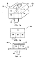
- Figs. 1a through 1c are views of an exemplary patch antenna with a selectable operating frequency.
- Fig. 1a is a perspective view of a single-band patch antenna that may have half-wavelength radiator dimensions.
- the patch antenna 100 comprises a counterpoise 102 and a dielectric with ferroelectric material 104 overlying the counterpoise.
- the dielectric has a varying dielectric constant responsive to a voltage applied to the ferroelectric material.
- At least one radiator 106 overlies the dielectric 104 having a resonant frequency responsive to the dielectric constant.
- the dielectric 104 is a layer consisting entirely of FE material.
- a coaxial feedline 108 has a center conductor 110 connected to the radiator 106 and a ground connected to the counterpoise 102.
- Fig. 1b is a plan view of the patch antenna 100 of Fig. 1a.
- the dielectric with FE material is only placed in the vicinity of the radiator 106.
- Area 112 may be a dielectric with a fixed constant.
- the FE dielectric 104 may surround the radiator 106 evenly on all sides, or the dielectric areas 104 and 112 may be formed symmetrically around the radiator 106.
- Fig. 1c is a cross-sectional view of an inverted-F planar antenna, such as might be suitable with quarter-wavelength radiator dimensions.
- the FE dielectric 104 is shown interposed between the single-radiator 106 and the counterpoise 102, however, other FE dielectric patterns and distributions are also practical.
- the antenna 100 has a predetermined fixed characteristic impedance independent of the resonant frequency. That is, the input impedance remains 50 ohms for example, despite the operating frequency selected. Alternately, it can be said that the antenna 100 has a predetermined approximately constant gain independent of the resonant frequency.
- Fig. 2 is a cross-sectional drawing illustrating an alternate aspect of the patch antenna of Fig. 1a.
- the dielectric 104 includes at least one dielectric layer 200 formed from a first material with a fixed dielectric constant and a dielectric 202 formed from a ferroelectric material with a variable dielectric constant, adjacent the dielectric 200 with the fixed dielectric constant.
- the dielectric with the FE material 202 overlies the dielectric with the fixed dielectric constant 200.
- a voltage is applied to a conductor in the vicinity of the FE dielectric layer 202 to create a desired dielectric constant.
- the voltage represented by the "+" and "-" signs can be supplied by voltage generator 203.
- an electrical insulator (not shown) can be interposed between layer 202 and the conductive radiator 106 to isolate the bias voltage from the ac signal voltage.
- a sheet of conductor is usually required to evenly distribute the bias voltage over the FE dielectric 202 that interferes with the antenna tuning. Therefore, the dc voltage is typically superimposed upon ac signal being conducted by the radiator, and the reference ground is supplied to the counterpoise 102.
- the dielectric formed with the fixed dielectric constant 200 overlies the dielectric with the ferroelectric material 202.
- an insulator might be interposed between the FE dielectric layer 202 and the conductive counterpoise, and a reference ground supplied that is different from the voltage at the counterpoise.
- the FE dielectric layer is typically biased with a reference ground supplied to the counterpoise. Note, in some aspects of the antenna the bias voltage polarities are reversed from the polarity shown.
- Fig. 3 is a cross-sectional drawing illustrating an alternate aspect of the patch antenna of Fig. 1a with multiple fixed dielectric constant layers.
- the dielectric with the fixed dielectric forms a first layer 200a underlying the dielectric with the fixed dielectric constant 202, and a second layer 200b overlies the dielectric with the ferroelectric material 202.
- the two fixed dielectric layers need not necessarily have the same dielectric constant. Further, the use of three or more layers of fixed dielectric is also possible.
- multiple FE layers can be formed around a fixed dielectric layer, or multiple layers of both fixed dielectric and FE layers can be used.
- the multiple FE dielectric layers may have different thickness, be made of different FE materials, or otherwise have different dielectric constants with respect to the same voltage.
- Fig. 4 is a cross-sectional drawing illustrating the invention as an alternate aspect of the patch antenna of Fig. 1a with an internal layer of FE material.
- the dielectric with the ferroelectric material 202 is formed internal to the dielectric 200 with the fixed dielectric constant.
- the dielectric with the fixed dielectric constant 200 is formed internal to the FE dielectric 202.
- multiple internal FE dielectric regions could be used.
- the dielectric with ferroelectric material 202 is formed from barium strontium titanate, Ba x Sr 1-x TiO 3 (BSTO). However, alternate FE materials are well known and may perform equivalently.
- the dielectric with ferroelectric material 202 can be formed in a thin film layer having a thickness 206 in the range from 0.15 to 2 microns. Alternately, the dielectric with ferroelectric material 202 is formed in a thick film having a thickness 206 in the range from 1.5 to 1000 microns.
- the dielectric with ferroelectric material has a dielectric constant in the range between 100 and 5000 at zero volts. In other aspects, the dielectric formed from the first material with a fixed dielectric constant 200 and the dielectric formed from the ferroelectric material 202 have a composite dielectric constant in the range between 2 and 100 at zero volts.
- the dielectric constant of the FE material can be manipulated through doping and control of the Curie temperature (Tc).
- Some popular dopant materials are tungsten (W), manganese (Mn), and magnesium (Mg), introduced as oxides.
- W tungsten
- Mn manganese
- Mg magnesium
- An FE material has its greatest dielectric constant at Tc, with the dielectric falling off rapidly with changes of temperature in either direction. However, there is typically less change in dielectric constant for temperature above Tc. Therefore, the Tc of an FE material is typically chosen to be below the operating temperature seen by the dielectric material.
- An antenna built with a dielectric constant of 1 (air) has less loss than an antenna built with higher dielectric constant material.
- higher dielectric constant materials are often useful in reducing the size (the effective wavelength) of antennas.
- an antenna designer seeks a dielectric material with dielectric constant of less than 100.
- the FE material dielectric constants can be reduced by adding dopants at the cost of variability (less change in dielectric constant per bias volt). Suitable tradeoffs between Tc and doping can make practical a greater than 2:1 change in FE material dielectric for less than a volt change in bias voltage.
- each single-band slot antenna includes a counterpoise and a dielectric with ferroelectric material overlying the counterpoise.
- some slots antennas can be understood as just having a radiator, or having a virtual radiator and virtual counterpoise.
- a slot, formed in either the counterpoise or the radiator has an electrical length responsive to the dielectric constant and the dielectric has a varying dielectric constant responsive to a voltage applied to the ferroelectric material.
- a radiator overlies and is proximate to the dielectric.
- the radiator in each of the slot designs has a predetermined fixed characteristic impedance independent of the resonant frequency. That is, the electrical length of the slot(s) is constant with respect to the resonant frequency. Alternately, the radiator has a predetermined approximately constant gain independent of the resonant frequency. It is also generally true that the slot (or slots) have an electrical length that varies in response to the dielectric constant(s) to be either approximately one-half wavelength of the resonant frequency with respect to the dielectric, or approximately one-quarter wavelength of the resonant frequency with respect to the dielectric.
- the principles and design of slot antennas are well understood by those skilled in the art and are not repeated here in the interest of brevity. Although the use of FE material gives a slot antenna a wider range of selectable operating frequencies, the general principles of design are not changed by the present invention FE material.
- Fig. 5a is a perspective view of the present invention microstrip slot antenna 500.
- a counterpoise 502, a radiator 504, and a dielectric with ferroelectric material 506 form the microstrip.
- the dielectric with ferroelectric material 506 is located in the vicinity of the slot, as shown.
- Away from the slot a different dielectric 507 may be used with a fixed dielectric constant.
- a slot 508 is formed in the counterpoise 502. As shown, the slot 508 is transverse to the radiator 504, but it need not be.
- a plurality of slots are used.
- Fig. 5b is a cross-sectional drawing illustrating an alternate aspect of the microstrip slot antenna of Fig. 5a.
- the dielectric 506 includes at least one dielectric layer 510 formed from a first material with a fixed dielectric constant and a dielectric 512 formed from a ferroelectric material with a variable dielectric constant, adjacent the dielectric 510 with the fixed dielectric constant.
- the dielectric with the FE material 512 overlies the dielectric with the fixed dielectric constant 510.
- a voltage is applied to a conductor in the vicinity of the FE dielectric layer 512 to create a desired dielectric constant.
- the voltage represented by the "+" and "-" signs can be supplied.
- an electrical insulator (not shown) can be interposed between layer 512 and the conductive radiator 504 to isolate the bias voltage from the ac signal voltage.
- a sheet of conductor is usually required to evenly distribute the bias voltage over the FE dielectric 512 that interferes with the antenna tuning. Therefore, the dc voltage is typically superimposed upon ac signal being conducted by the radiator, and the reference ground is supplied to the counterpoise 502.
- the dielectric formed with the fixed dielectric constant 510 overlies the dielectric with the ferroelectric material 512.
- an insulator might be interposed between the FE dielectric layer 512 and the conductive counterpoise, and a reference ground supplied that is different from the voltage at the counterpoise.
- the FE dielectric layer is typically biased with a reference ground supplied to the counterpoise. Note, in some aspects of the antenna the bias voltage polarities are reversed from the polarities shown.
- Fig. 5c is a cross-sectional drawing illustrating an alternate aspect of the microstrip slot antenna of Fig. 5a with multiple fixed dielectric constant layers.
- the dielectric with the fixed dielectric forms a first layer 510a underlying the dielectric with the fixed dielectric constant 512, and a second layer 510b overlies the dielectric with the ferroelectric material 512.
- the two fixed dielectric layers need not necessarily have the same dielectric constant or thickness. Further, three or more fixed dielectric layers may be used. Alternately but not shown, multiple FE layers can be formed around a fixed dielectric layer, or multiple layers of both fixed dielectric and FE layers can be used.
- the multiple FE dielectric layers may have different thickness, be made of different FE materials, or otherwise have different dielectric constants with respect to the same voltage.
- Fig. 5d is a cross-sectional drawing illustrating the invention as an alternate aspect of the microstrip slot antenna of Fig. 5a with an internal layer of FE material.
- the dielectric with the ferroelectric material 512 is formed internal to the dielectric 510 with the fixed dielectric constant.
- multiple FE internal regions can be formed.
- the dielectric with the fixed dielectric constant 510 is formed internal to the FE dielectric 512.
- additional electrical insulators might be used to isolate from the counterpoise 502 and radiator 504 from the FE layer 512.
- the dielectric with ferroelectric material 512 is formed from barium strontium titanate, Ba x Sr 1-x TiO 3 (BSTO).
- BSTO barium strontium titanate
- alternate FE materials are well known and may perform equivalently.
- the dielectric with ferroelectric material 512 can be formed in a thin film layer having a thickness 514 in the range from 0.15 to 2 microns.
- the dielectric with ferroelectric material 512 is formed in a thick film having a thickness 514 in the range from 1.5 to 1000 microns.
- the dielectric with ferroelectric material has a dielectric constant in the range between 100 and 5000 at zero volts.
- the dielectric formed from the first material with a fixed dielectric constant and the dielectric formed from the ferroelectric material have a composite dielectric constant in the range between 2 and 100 at zero volts.
- the dielectric constant of the FE material can be manipulated through doping and control of the Curie temperature (Tc).
- Some popular dopant materials are tungsten (W), manganese (Mn), and magnesium (Mg), introduced as oxides.
- W tungsten
- Mn manganese
- Mg magnesium
- An FE material has its greatest dielectric constant at Tc, with the dielectric falling off rapidly with changes of temperature in either direction. However, there is typically less change in dielectric constant for temperature above Tc. Therefore, the Tc of an FE material is typically chosen to be below the operating temperature seen by the dielectric material.
- An antenna built with a dielectric constant of 1 (air) has less loss than an antenna built with higher dielectric constant material.
- higher dielectric constant materials are often useful in reducing the size (the effective wavelength) of antennas.
- an antenna designer seeks a dielectric material with dielectric constant of less than 100.
- the FE material dielectric constants can be reduced by adding dopants at the cost of variability (less change in dielectric constant per bias volt). Suitable tradeoffs between Tc and doping can make practical a greater than 2:1 change in FE material dielectric for less than a volt change in bias voltage.
- Fig. 6a is a perspective view of a coaxial slot antenna 600 which is not part of the invention.
- the counterpoise 602, radiator 604, and dielectric with FE material 606 form a coaxial line with a slot 608 in the counterpoise 602.
- the FE dielectric 606 is proximate to the slot 608. Away from the slot a different dielectric 607 with a fixed dielectric constant can be used. As shown, the slot 608 is transverse to the radiator 604, but it need not be.
- a plurality of slots are used.
- Fig. 6b is a cross-sectional drawing illustrating an alternate aspect of the coaxial slot antenna of Fig. 6a.
- the dielectric 606 includes at least one dielectric layer 610 formed from a first material with a fixed dielectric constant and a dielectric 612 formed from a ferroelectric material with a variable dielectric constant, adjacent the dielectric 610 with the fixed dielectric constant.
- the dielectric with the FE material 612 overlies the dielectric with the fixed dielectric constant 610.
- a voltage is applied to a conductor in the vicinity of the FE dielectric layer 612 to create a desired dielectric constant.
- the voltage represented by the "+" and "-" signs can be supplied.
- an electrical insulator (not shown) can be interposed between layer 612 and the conductive radiator 604 to isolate the bias voltage from the ac signal voltage.
- a sheet of conductor is usually required to evenly distribute the bias voltage over the FE dielectric 612 that interferes with the antenna tuning. Therefore, the dc voltage is typically superimposed upon ac signal being conducted by the radiator, and the reference ground is supplied to the counterpoise 602.
- the dielectric formed with the fixed dielectric constant 610 overlies the dielectric with the ferroelectric material 612.
- an insulator might be interposed between the FE dielectric layer 612 and the conductive counterpoise, and a reference ground supplied that is different from the voltage at the counterpoise.
- the FE dielectric layer is typically biased with a reference ground supplied to the counterpoise. Note, in some aspects of the antenna the bias voltage polarities are reversed from the polarities shown.
- Fig. 6c is a cross-sectional drawing illustrating an alternate aspect of the coaxial slot antenna of Fig. 6a with multiple fixed dielectric constant layers.
- the dielectric with the fixed dielectric forms a first layer 610a underlying the dielectric with the fixed dielectric constant 612, and a second layer 610b overlies the dielectric with the ferroelectric material 612.
- the two fixed dielectric layers need not necessarily have the same dielectric constant or thickness. Further, three or more fixed dielectric layers may be used. Alternately but not shown, multiple FE layers can be formed around a fixed dielectric layer, or multiple layers of both fixed dielectric and FE layers can be used.
- the multiple FE dielectric layers may have different thickness, be made of different FE materials, or otherwise have different dielectric constants with respect to the same voltage.
- Fig. 6d is a cross-sectional drawing illustrating an alternate aspect of the coaxial slot antenna of Fig. 6a with an internal layer of FE material.
- the dielectric with the ferroelectric material 612 is formed internal to the dielectric 610 with the fixed dielectric constant. Note, multiple internal regions can be formed although only one is shown. Alternately but not shown, the dielectric with the fixed dielectric constant 610 is formed internal to the FE dielectric 612. Again, additional electrical insulators might be used to isolate from the counterpoise 602 and radiator 604 from the FE layer 612.
- the dielectric with ferroelectric material 612 is formed from barium strontium titanate, Ba x Sr 1-x TiO 3 (BSTO). However, alternate FE materials are well known and may perform equivalently.
- the dielectric with ferroelectric material 612 can be formed in a thin film layer having a thickness 614 in the range from 0.15 to 2 microns. Alternately, the dielectric with ferroelectric material 612 is formed in a thick film having a thickness 614 in the range from 1.5 to 1000 microns.
- the dielectric with ferroelectric material has a dielectric constant in the range between 100 and 5000 at zero volts. In other aspects, the dielectric formed from the first material with a fixed dielectric constant and the dielectric formed from the ferroelectric material have a composite dielectric constant in the range between 2 and 100 at zero volts.
- the dielectric constant of the FE material can be manipulated through doping and control of the Curie temperature (Tc).
- Some popular dopant materials are tungsten (W), manganese (Mn), and magnesium (Mg), introduced as oxides.
- W tungsten
- Mn manganese
- Mg magnesium
- An FE material has its greatest dielectric constant at Tc, with the dielectric falling off rapidly with changes of temperature in either direction. However, there is typically less change in dielectric constant for temperature above Tc. Therefore, the Tc of an FE material is typically chosen to be below the operating temperature seen by the dielectric material.
- An antenna built with a dielectric constant of 1 (air) has less loss than an antenna built with higher dielectric constant material.
- higher dielectric constant materials are often useful in reducing the size (the effective wavelength) of antennas.
- an antenna designer seeks a dielectric material with dielectric constant of less than 100.
- the FE material dielectric constants can be reduced by adding dopants at the cost of variability (less change in dielectric constant per bias volt). Suitable tradeoffs between Tc and doping can make practical a greater than 2:1 change in FE material dielectric for less than a volt change in bias voltage.
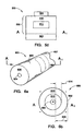
- Figs. 7a through 7f are exemplary views of a circular waveguide slot antenna 700 which is not part of the invention.
- the circular waveguide antenna is described as comprising a radiator 704 and dielectric 706.
- the slot 708 is transverse to the radiator 704, but it need not be.
- the FE dielectric 706 is located proximate to the slot 708.
- Other, fixed constant dielectric material 707 can be used away from the slot 708.
- a plurality of slots are used.
- Fig. 7b is a cross-sectional drawing illustrating an alternate aspect of the circular waveguide slot antenna of Fig. 7a.
- the dielectric 706 includes at least one dielectric layer 710 formed from a first material with a fixed dielectric constant and a dielectric 712 formed from a ferroelectric material with a variable dielectric constant, adjacent the dielectric 710 with the fixed dielectric constant.
- the dielectric with the FE material 712 overlies the dielectric with the fixed dielectric constant 710.
- a voltage is applied to a conductor in the vicinity of the FE dielectric layer 712 to create a desired dielectric constant.
- the voltage represented by the "+" and "-" signs can be supplied.
- an electrical insulator (not shown) can be interposed between layer 712 and the conductive radiator 704 to isolate the bias voltage from the ac signal voltage.
- a sheet of conductor is usually required to evenly distribute the bias voltage over the FE dielectric 712 that interferes with the antenna tuning. Therefore, slits 709 can be formed in the radiator 704 to separate the two bias voltage polarities.
- the dc voltages are typically superimposed upon ac signal being conducted by the radiator halves.
- the dielectric formed with the fixed dielectric constant 710 overlies the dielectric with the ferroelectric material 712. Note, in some aspects of the antenna the bias voltage polarities are reversed from the polarities shown.
- Fig. 7c is a cross-sectional drawing illustrating an alternate aspect of the circular waveguide slot antenna of Fig. 7a with multiple fixed dielectric constant layers.
- the dielectric with the fixed dielectric forms a first layer 710a underlying the dielectric with the fixed dielectric constant 712, and a second layer 710b overlies the dielectric with the ferroelectric material 712.
- the two fixed dielectric layers need not necessarily have the same dielectric constant or thickness. Further, three or more fixed dielectric layers may be used. Alternately but not shown, multiple FE layers can be formed around a fixed dielectric layer, or multiple layers of both fixed dielectric and FE layers can be used.
- the multiple FE dielectric layers may have different thickness, be made of different FE materials, or otherwise have different dielectric constants with respect to the same voltage.
- Fig. 7d is a cross-sectional drawing illustrating an alternate aspect of the circular waveguide slot antenna of Fig. 7a with an internal layer of FE material.
- the dielectric with the ferroelectric material 712 is formed internal to the dielectric 710 with the fixed dielectric constant. Note, multiple internal regions can be formed although only one is shown. Alternately but not shown, the dielectric with the fixed dielectric constant 710 is formed internal to the FE dielectric 712. It should also be noted that although the internal region is shown as rectangularly shaped, other shapes such as circular, cylindrical, and oval shapes are equally practical.
- Figs. 7e and 7f are alternate aspects of the circular waveguide slot antenna 700.
- the slits are not necessary because the radiator 704 need not carry a bias voltage. Instead the bias voltage is supplied by panels 714 and 716.
- the bias panels 714/716 can be placed in a variety of positions on either side of the FE dielectric. One panel may even be located in the slot.
- the dielectric with ferroelectric material 712 is formed from barium strontium titanate, Ba x Sr 1-x TiO 3 (BSTO). However, alternate FE materials are well known and may perform equivalently.
- the dielectric with ferroelectric material 712 can be formed in a thin film layer having a thickness 714 in the range from 0.15 to 2 microns. Alternately, the dielectric with ferroelectric material 712 is formed in a thick film having a thickness 714 in the range from 1.5 to 1000 microns.
- the dielectric with ferroelectric material has a dielectric constant in the range between 100 and 5000 at zero volts. In other aspects, the dielectric formed from the first material with a fixed dielectric constant and the dielectric formed from the ferroelectric material have a composite dielectric constant in the range between 2 and 100 at zero volts.
- the dielectric constant of the FE material can be manipulated through doping and control of the Curie temperature (Tc).
- Some popular dopant materials are tungsten (W), manganese (Mn), and magnesium (Mg), introduced as oxides.
- W tungsten
- Mn manganese
- Mg magnesium
- An FE material has its greatest dielectric constant at Tc, with the dielectric falling off rapidly with changes of temperature in either direction. However, there is typically less change in dielectric constant for temperature above Tc. Therefore, the Tc of an FE material is typically chosen to be below the operating temperature seen by the dielectric material.
- An antenna built with a dielectric constant of 1 (air) has less loss than an antenna built with higher dielectric constant material.
- higher dielectric constant materials are often useful in reducing the size (the effective wavelength) of antennas.
- an antenna designer seeks a dielectric material with dielectric constant of less than 100.
- the FE material dielectric constants can be reduced by adding dopants at the cost of variability (less change in dielectric constant per bias volt). Suitable tradeoffs between Tc and doping can make practical a greater than 2:1 change in FE material dielectric for less than a volt change in bias voltage.
- Fig. 8a is a perspective view of an exemplary rectangular waveguide slot antenna 800 which is not part of the invention.
- the rectangular waveguide antenna is described as comprising a radiator 804 and dielectric 806. However, the designations of radiator and counterpoise are arbitrary.
- the slot 808 is transverse to the radiator 804, but it need not be.
- the FE dielectric 806 is located proximate to the slot 808. Away from the slot 808, a fixed constant dielectric 807 may be used.
- a plurality of slots are used.
- Fig. 8b is a cross-sectional drawing illustrating an alternate aspect of the rectangular waveguide slot antenna of Fig. 8a.
- the dielectric 806 includes at least one dielectric layer 810 formed from a first material with a fixed dielectric constant and a dielectric 812 formed from a ferroelectric material with a variable dielectric constant, adjacent the dielectric 810 with the fixed dielectric constant.
- the dielectric with the FE material 812 overlies the dielectric with the fixed dielectric constant 810.
- a voltage is applied to a conductor in the vicinity of the FE dielectric layer 812 to create a desired dielectric constant.
- the voltage represented by the "+" and "-" signs can be supplied.
- an electrical insulator (not shown) can be interposed between layer 812 and the conductive radiator 804 to isolate the bias voltage from the ac signal voltage.
- a sheet of conductor is usually required to evenly distribute the bias voltage over the FE dielectric 812 that interferes with the antenna tuning. Therefore, (electrically isolating) slits 809 can be formed in the radiator 804 to separate the two bias voltage polarities. The dc voltages are typically superimposed upon ac signal being conducted by the radiator halves.
- the dielectric formed with the fixed dielectric constant 810 overlies the dielectric with the ferroelectric material 812. Note, in some aspects of the antenna the bias voltage polarities are reversed from the polarities shown.
- Fig. 8c is a cross-sectional drawing illustrating an alternate aspect of the rectangular waveguide slot antenna of Fig. 8a with multiple fixed dielectric constant layers.
- the dielectric with the fixed dielectric forms a first layer 810a underlying the dielectric with the fixed dielectric constant 812, and a second layer 810b overlies the dielectric with the ferroelectric material 812.
- the two fixed dielectric layers need not necessarily have the same dielectric constant or thickness. Further, three or more fixed dielectric layers may be used. Alternately but not shown, multiple FE layers can be formed around a fixed dielectric layer, or multiple layers of both fixed dielectric and FE layers can be used.
- the multiple FE dielectric layers may have different thickness, be made of different FE materials, or otherwise have different dielectric constants with respect to the same voltage.
- Fig. 8d is a cross-sectional drawing illustrating an alternate aspect of the rectangular waveguide slot antenna of Fig. 8a with an internal layer of FE material.
- the dielectric with the ferroelectric material 812 is formed internal to the dielectric 810 with the fixed dielectric constant. Note, multiple internal regions can be formed although only one is shown. Alternately but not shown, the dielectric with the fixed dielectric constant 810 is formed internal to the FE dielectric 812. It should also be noted that although the internal region is shown as rectangularly shaped, other shapes such as circular, cylindrical, and oval shapes are equally practical.
- the dc bias voltage is supplied by panels interior to the radiator 804, so that the slits 809 need not be formed.
- the dielectric with ferroelectric material 812 is formed from barium strontium titanate, Ba x Sr 1-x TiO 3 (BSTO). However, alternate FE materials are well known and may perform equivalently.
- the dielectric with ferroelectric material 812 can be formed in a thin film layer having a thickness 814 in the range from 0.15 to 2 microns. Alternately, the dielectric with ferroelectric material 812 is formed in a thick film having a thickness 814 in the range from 1.5 to 1000 microns.
- the dielectric with ferroelectric material has a dielectric constant in the range between 100 and 5000 at zero volts. In other aspects, the dielectric formed from the first material with a fixed dielectric constant and the dielectric formed from the ferroelectric material have a composite dielectric constant in the range between 2 and 100 at zero volts.
- the dielectric constant of the FE material can be manipulated through doping and control of the Curie temperature (Tc).
- Some popular dopant materials are tungsten (W), manganese (Mn), and magnesium (Mg), introduced as oxides.
- W tungsten
- Mn manganese
- Mg magnesium
- An FE material has its greatest dielectric constant at Tc, with the dielectric falling off rapidly with changes of temperature in either direction. However, there is typically less change in dielectric constant for temperature above Tc. Therefore, the Tc of an FE material is typically chosen to be below the operating temperature seen by the dielectric material.
- An antenna built with a dielectric constant of 1 (air) has less loss than an antenna built with higher dielectric constant material.
- higher dielectric constant materials are often useful in reducing the size (the effective wavelength) of antennas.
- an antenna designer seeks a dielectric material with dielectric constant of less than 100.
- the FE material dielectric constants can be reduced by adding dopants at the cost of variability (less change in dielectric constant per bias volt). Suitable tradeoffs between Tc and doping can make practical a greater than 2:1 change in FE material dielectric for less than a volt change in bias voltage.
- Figs. 9a and 9b are partial cross-sectional and plan views, respectively, of an exemplary flare-notch antenna which is not part of the invention.
- the flare-notch antenna 900 comprises a counterpoise 902, a radiator 904, and a dielectric 906a and 906a, at least one of which including FE material.
- the designation of counterpoise and radiator may be considered arbitrary.
- a slot or notch 907 is shown.
- the FE dielectric 906a and 906b are proximately located to the notch 907. Also shown is a feed with a center conductor 908 and a ground 909.
- Fig, 9c is an alternate aspect of the flare-notch antenna of Fig. 9b.
- the dielectric 906a and 906b includes at least one dielectric layer 910 formed from a first material with a fixed dielectric constant and a dielectric 912 formed from a ferroelectric material with a variable dielectric constant, adjacent the dielectric 910 with the fixed dielectric constant.
- the dielectric with the FE material 912 overlies the dielectric with the fixed dielectric constant 910.
- a voltage is applied to a conductor in the vicinity of the FE dielectric layer 912 to create a desired dielectric constant.
- the voltage represented by the "+" and "-" signs can be supplied.
- an electrical insulator (not shown) can be interposed between layer 912 and the radiator/counterpoise 904/902 to isolate the bias voltage from the ac signal voltage.
- a sheet of conductor is usually required to evenly distribute the bias voltage over the FE dielectric 912 that interferes with the antenna tuning. Therefore, the dc voltage is typically superimposed upon ac signal being conducted by the radiator/counterpoise 904/902, and the reference ground is supplied to conductive panels 914.
- the dielectric formed with the fixed dielectric constant 910 overlies the dielectric with the ferroelectric material 912. Note, in some aspects of the antenna the bias voltage polarities are reversed from the polarity shown.
- Fig. 9d is a plan view illustrating an alternate aspect of the flare-notch antenna of Fig. 9b with multiple fixed dielectric constant layers.
- the dielectric with the fixed dielectric forms a first layer 910a underlying the dielectric with the fixed dielectric constant 912, and a second layer 910b overlies the dielectric with the ferroelectric material 912.
- the two fixed dielectric layers need not necessarily have the same dielectric constant or thickness. Further, three or more fixed dielectric layers may be used. Alternately but not shown, multiple FE layers can be formed around a fixed dielectric layer, or multiple layers of both fixed dielectric and FE layers can be used. The multiple FE dielectric layers may have different thickness, be made of different FE materials, or otherwise have different dielectric constants with respect to the same voltage.
- Fig. 9e is a plan view illustrating an alternate aspect of the flare-notch antenna of Fig. 9b with an internal layer of FE material.
- the dielectric with the ferroelectric material 912 is formed internal to the dielectric 910 with the fixed dielectric constant. Note, multiple internal regions can be formed although only one is shown. Alternately but not shown, the dielectric with the fixed dielectric constant 910 is formed internal to the FE dielectric 912. It should also be noted that although the internal region is shown as rectangularly shaped, other shapes such as circular, cylindrical, and oval shapes are equally practical. In another variation not shown, the FE material forms internal regions on only one side of the radiator, for example is dielectric 906a.
- the dielectric with ferroelectric material 912 is formed from barium strontium titanate, Ba x Sr 1-x TiO 3 (BSTO). However, alternate FE materials are well known and may perform equivalently.
- the dielectric with ferroelectric material 912 can be formed in a thin film layer having a thickness 914 in the range from 0.15 to 2 microns. Alternately, the dielectric with ferroelectric material 912 is formed in a thick film having a thickness 914 in the range from 1.5 to 1000 microns.
- the dielectric with ferroelectric material has a dielectric constant in the range between 100 and 5000 at zero volts. In other aspects, the dielectric formed from the first material with a fixed dielectric constant and the dielectric formed from the ferroelectric material have a composite dielectric constant in the range between 2 and 100 at zero volts.
- the dielectric constant of the FE material can be manipulated through doping and control of the Curie temperature (Tc).
- Some popular dopant materials are tungsten (W), manganese (Mn), and magnesium (Mg), introduced as oxides.
- W tungsten
- Mn manganese
- Mg magnesium
- An FE material has its greatest dielectric constant at Tc, with the dielectric falling off rapidly with changes of temperature in either direction. However, there is typically less change in dielectric constant for temperature above Tc. Therefore, the Tc of an FE material is typically chosen to be below the operating temperature seen by the dielectric material.
- An antenna built with a dielectric constant of 1 (air) has less loss than an antenna built with higher dielectric constant material.
- higher dielectric constant materials are often useful in reducing the size (the effective wavelength) of antennas.
- an antenna designer seeks a dielectric material with dielectric constant of less than 100.
- the FE material dielectric constants can be reduced by adding dopants at the cost of variability (less change in dielectric constant per bias volt). Suitable tradeoffs between Tc and doping can make practical a greater than 2:1 change in FE material dielectric for less than a volt change in bias voltage.
- Figs. 10a though 10d are illustrations of an exemplary open-ended waveguide antenna 1000 which is not part of the invention.
- Fig. 10a is a partial cross-sectional view of the present invention open-ended waveguide antenna with a selectable operating frequency.
- the open-ended waveguide antenna 1000 comprises a radiator 1002 and a dielectric 1006 with ferroelectric material proximately located to the radiator 1002.
- the dielectric 1006 has a varying dielectric constant responsive to a voltage applied to the ferroelectric material.
- the designations of counterpoise and radiator are arbitrary.
- the open ends 1007 are grounded. Away from the open ends 107 a constant dielectric material 1005 can be used.
- open-ended antennas are well understood by those skilled in the art and are not repeated here in the interest of brevity. Although the use of FE material gives an open-ended antenna a wider range of selectable operating frequencies, the general principles of design are not changed by the present invention FE material.
- the antenna 1000 has a predetermined fixed characteristic impedance independent of the resonant frequency. Alternately stated, the antenna 1000 has a predetermined approximately constant gain independent of the resonant frequency.
- Fig. 10b is a cross-sectional drawing illustrating an alternate aspect of the open-ended waveguide antenna of Fig. 10a.
- the dielectric 1006 includes at least one dielectric layer 1010 formed from a first material with a fixed dielectric constant and a dielectric 1012 formed from a ferroelectric material with a variable dielectric constant, adjacent the dielectric 1010 with the fixed dielectric constant.
- the dielectric with the FE material 1012 overlies the dielectric with the fixed dielectric constant 1010.
- a voltage is applied to a conductor in the vicinity of the FE dielectric layer 1012 to create a desired dielectric constant.
- the voltage represented by the "+" and "-" signs can be supplied.
- an electrical insulator (not shown) can be interposed between layer 1012 and the radiator 1002 to isolate the bias voltage from the ac signal voltage.
- a sheet of conductor is usually required to evenly distribute the bias voltage over the FE dielectric 1012 that interferes with the antenna tuning. Therefore, electrically isolating slits 1009 can be formed in the radiator 1002 to separate the two bias voltage polarities.
- the dc voltages are typically superimposed upon ac signal being conducted by the radiator halves.
- the dielectric formed with the fixed dielectric constant 1010 overlies the dielectric with the ferroelectric material 1012. Note, in some aspects of the antenna the bias voltage polarities are reversed from the polarity shown.
- Fig. 10c is a cross-sectional drawing illustrating an alternate aspect of the open-ended waveguide antenna of Fig. 10a with multiple fixed dielectric constant layers.
- the dielectric with the fixed dielectric forms a first layer 1010a underlying the dielectric with the fixed dielectric constant 1012, and a second layer 1010b overlies the dielectric with the ferroelectric material 1012.
- the two fixed dielectric layers need not necessarily have the same dielectric constant or thickness. Further, three or more fixed dielectric layers may be used. Alternately but not shown, multiple FE layers can be formed around a fixed dielectric layer, or multiple layers of both fixed dielectric and FE layers can be used.
- the multiple FE dielectric layers may have different thickness, be made of different FE materials, or otherwise have different dielectric constants with respect to the same voltage.
- Fig. 10d is a cross-sectional drawing illustrating an alternate aspect of the open-ended waveguide antenna of Fig. 10a with an internal layer of FE material.
- the dielectric with the ferroelectric material 1012 is formed internal to the dielectric 1010 with the fixed dielectric constant. Note, multiple internal regions can be formed although only one is shown. Alternately but not shown, the dielectric with the fixed dielectric constant 1010 is formed internal to the FE dielectric 1012. It should also be noted that although the internal region is shown as rectangularly shaped, other shapes such as circular, cylindrical, and oval shapes are equally practical.
- the dc bias voltage is supplied by panels interior to the radiator 1002, so that the slits 1009 need not be formed.
- the dielectric with ferroelectric material 1012 is formed from barium strontium titanate, Ba x Sr 1-x TiO 3 (BSTO). However, alternate FE materials are well known and may perform equivalently.
- the dielectric with ferroelectric material 1012 is formed in a thin film layer having a thickness 1014 in the range from 0.15 to 2 microns. Alternately, the dielectric with ferroelectric material 1012 is formed in a thick film having a thickness 1014 in the range from 1.5 to 1000 microns.
- the dielectric with ferroelectric material has a dielectric constant in the range between 100 and 5000 at zero volts. In other aspects, the dielectric formed from the first material with a fixed dielectric constant and the dielectric formed from the ferroelectric material have a composite dielectric constant in the range between 2 and 100 at zero volts.
- the dielectric constant of the FE material can be manipulated through doping and control of the Curie temperature (Tc).
- Some popular dopant materials are tungsten (W), manganese (Mn), and magnesium (Mg), introduced as oxides.
- W tungsten
- Mn manganese
- Mg magnesium
- An FE material has its greatest dielectric constant at Tc, with the dielectric falling off rapidly with changes of temperature in either direction. However, there is typically less change in dielectric constant for temperature above Tc. Therefore, the Tc of an FE material is typically chosen to be below the operating temperature seen by the dielectric material.
- An antenna built with a dielectric constant of 1 (air) has less loss than an antenna built with higher dielectric constant material.
- higher dielectric constant materials are often useful in reducing the size (the effective wavelength) of antennas.
- an antenna designer seeks a dielectric material with dielectric constant of less than 100.
- the FE material dielectric constants can be reduced by adding dopants at the cost of variability (less change in dielectric constant per bias volt). Suitable tradeoffs between Tc and doping can make practical a greater than 2:1 change in FE material dielectric for less than a volt change in bias voltage.
- open-ended rectangular waveguide has been depicted, the above analysis and description applies to open-ended circular waveguide and open-ended parallel plate antennas. Further, the open-ended waveguide antenna 1000 can have a signal feed elected that is a coaxial cable, parallel plates, or any kind of waveguide.
- Figs. 11a through 11e are views of an exemplary horn antenna with a selectable operating frequency which is not part of the invention.
- the horn antenna 1100 comprises a radiator horn 1102 and a dielectric 1106 with ferroelectric material proximately located to the radiator horn.
- the dielectric 1006 has a varying dielectric constant responsive to a voltage applied to the ferroelectric material.
- a coaxial feed line 1004 with a center conductor 1005 is shown.
- the horn 1002 has an electrical length 1109 responsive to the dielectric constant. The electrical length is constant with respect to the resonant frequency.
- the horn can be either grounded or open. Again the designations of counterpoise and radiator are arbitrary.
- horn antennas are well understood by those skilled in the art and are not repeated here in the interest of brevity. Although the use of FE material gives a horn antenna a wider range of selectable operating frequencies, the general principles of design are not changed by the present invention FE material.
- the horn antenna 1100 has a predetermined fixed characteristic impedance independent of the resonant frequency. Alternately, the horn antenna 1100 has a predetermined approximately constant gain independent of the resonant frequency.
- Fig. 11b is a cross-sectional drawing illustrating an alternate aspect of the horn antenna of Fig. 11a.
- the dielectric 1106 includes at least one dielectric layer 1110 formed from a first material with a fixed dielectric constant and a dielectric 1112 formed from a ferroelectric material with a variable dielectric constant, adjacent the dielectric 1110 with the fixed dielectric constant.
- the dielectric with the FE material 1112 overlies the dielectric with the fixed dielectric constant 1110.
- a voltage is applied to a conductor in the vicinity of the FE dielectric layer 1112 to create a desired dielectric constant.
- the voltage represented by the "+" and "-" signs can be supplied.
- an electrical insulator (not shown) can be interposed between layer 1112 and the radiator horn 1102 to isolate the bias voltage from the ac signal voltage.
- a sheet of conductor is usually required to evenly distribute the bias voltage over the FE dielectric 1112 that interferes with the antenna tuning. Therefore, electrically isolating slits 1108 can be formed in the radiator 1102 to separate the two bias voltage polarities.
- the dc voltages are typically superimposed upon ac signal being conducted by the radiator halves.
- the dielectric formed with the fixed dielectric constant 1110 overlies the dielectric with the ferroelectric material 1112. Note, in some aspects of the antenna the bias voltage polarities are reversed from the polarities shown.
- Fig. 11c and 11d are cross-sectional drawings illustrating an alternate aspect of the horn antenna 1100 of Fig. 11a with multiple fixed dielectric constant layers.
- the dielectric with the fixed dielectric forms a first layer 1110a underlying the dielectric with the fixed dielectric constant 1112, and a second layer 1110b overlies the dielectric with the ferroelectric material 1112.
- the two fixed dielectric layers need not necessarily have the same dielectric constant or thickness. Further, three or more fixed dielectric layers may be used. Alternately but not shown, multiple FE layers can be formed around a fixed dielectric layer, or multiple layers of both fixed dielectric and FE layers can be used.
- the multiple FE dielectric layers may have different thickness, be made of different FE materials, or otherwise have different dielectric constants with respect to the same voltage.
- Fig. 11e is a cross-sectional drawing illustrating an alternate aspect of the horn antenna of Fig. 11a with an internal layer of FE material.
- the dielectric with the ferroelectric material 1112 is formed internal to the dielectric 1110 with the fixed dielectric constant.
- multiple internal regions can be formed although only one is shown.
- the dielectric with the fixed dielectric constant 1110 is formed internal to the FE dielectric 1112.
- the internal region is shown as rectangularly shaped, other shapes such as circular, cylindrical, and oval shapes are equally practical.
- the dc bias voltage is supplied by panels interior to the radiator 1002, so that the slits 1108 need not be formed.
- the dielectric with ferroelectric material 1112 is formed from barium strontium titanate, Ba x Sr 1-x TiO 3 (BSTO). However, alternate FE materials are well known and may perform equivalently.
- the dielectric with ferroelectric material 1112 can be formed in a thin film layer having a thickness 1114 in the range from 0.15 to 2 microns. Alternately, the dielectric with ferroelectric material 1112 is formed in a thick film having a thickness 1114 in the range from 1.5 to 1000 microns.
- the dielectric with ferroelectric material has a dielectric constant in the range between 100 and 5000 at zero volts. In other aspects, the dielectric formed from the first material with a fixed dielectric constant and the dielectric formed from the ferroelectric material have a composite dielectric constant in the range between 2 and 100 at zero volts.
- the dielectric constant of the FE material can be manipulated through doping and control of the Curie temperature (Tc).
- Some popular dopant materials are tungsten (W), manganese (Mn), and magnesium (Mg), introduced as oxides.
- W tungsten
- Mn manganese
- Mg magnesium
- An FE material has its greatest dielectric constant at Tc, with the dielectric falling off rapidly with changes of temperature in either direction. However, there is typically less change in dielectric constant for temperature above Tc. Therefore, the Tc of an FE material is typically chosen to be below the operating temperature seen by the dielectric material.
- An antenna built with a dielectric constant of 1 (air) has less loss than an antenna built with higher dielectric constant material.
- higher dielectric constant materials are often useful in reducing the size (the effective wavelength) of antennas.
- an antenna designer seeks a dielectric material with dielectric constant of less than 100.
- the FE material dielectric constants can be reduced by adding dopants at the cost of variability (less change in dielectric constant per bias volt). Suitable tradeoffs between Tc and doping can make practical a greater than 2:1 change in FE material dielectric for less than a volt change in bias voltage.
- horn antennas applies equally to rectangular waveguide, circular waveguide, and parallel plate horn antennas using a signal feed from a coaxial cable, circular waveguide, rectangular waveguide, or a parallel plate signal feed.
- the monopole antenna 1200 comprises a radiator 1202, a counterpoise 1204, and a dielectric 1206 at least partially surrounding the radiator 1202.
- the dielectric includes ferroelectric material having a varying dielectric constant responsive to a voltage applied to the ferroelectric material.
- the radiator 1202 has an electrical length 1208 responsive to the dielectric constant. Alternately but not shown, the radiator 1202 can be formed in a helical shape.
- the principles and design of monopole antennas are well understood by those skilled in the art and are not repeated here in the interest of brevity. Although the use of FE material gives a monopole antenna a wider range of selectable operating frequencies, the general principles of design are not changed by the present invention FE material.
- the antenna 1200 has a predetermined fixed characteristic impedance independent of the resonant frequency. That is, the electrical length of the radiator is constant with respect to the resonant frequency. Alternately, the antenna 1200 has a predetermined approximately constant gain independent of the resonant frequency.
- Fig. 12b is a drawing illustrating an alternate aspect of the monopole antenna of Fig. 12a.
- the dielectric 1206 includes at least one dielectric layer 1210 formed from a first material with a fixed dielectric constant and a dielectric 1212 formed from a ferroelectric material with a variable dielectric constant, adjacent the dielectric 1210 with the fixed dielectric constant.
- the dielectric with the FE material 1212 overlies the dielectric with the fixed dielectric constant 1210.
- a voltage is applied to a conductor in the vicinity of the FE dielectric layer 1212 to create a desired dielectric constant.
- the voltage represented by the "+" and "-" signs can be supplied.
- an electrical insulator (not shown) can be interposed between layer 1212 and the radiator 1202 to isolate the bias voltage from the ac signal voltage.
- a sheet of conductor is usually required to evenly distribute the bias voltage over the FE dielectric 1212 that interferes with the antenna tuning. Therefore, the dc voltage is typically superimposed upon ac signal being conducted by the radiator 1202, and the reference ground is supplied to conductive panels 1214. Note, in some aspects of the antenna the bias voltage polarities are reversed. In other aspects, the radiator 1202 does not carry a dc bias, the two bias polarities are carried instead by panels 1214.
- Fig. 12c is a drawing illustrating an alternate aspect of the monopole antenna 1200 of Fig. 12a with multiple fixed dielectric constant layers.
- the dielectric with the fixed dielectric forms a first layer 1210a underlying the dielectric with the fixed dielectric constant 1212, and a second layer 1210b overlies the dielectric with the ferroelectric material 1212.
- the two fixed dielectric layers need not necessarily have the same dielectric constant or thickness. Further, three or more fixed dielectric layers may be used. Alternately but not shown, multiple FE layers can be formed around a fixed dielectric layer, or multiple layers of both fixed dielectric and FE layers can be used. The multiple FE dielectric layers may have different thickness, be made of different FE materials, or otherwise have different dielectric constants with respect to the same voltage.
- Fig. 12d is a drawing illustrating an alternate aspect of the monopole antenna of Fig. 12a with an internal layer of FE material.
- the dielectric with the ferroelectric material 1212 is formed internal to the dielectric 1210 with the fixed dielectric constant. Note, multiple internal regions can be formed although only one is shown. Alternately but not shown, the dielectric with the fixed dielectric constant 1210 is formed internal to the FE dielectric 1212. It should also be noted that although the internal region is shown as rectangularly shaped, other shapes such as circular, cylindrical, and oval shapes are equally practical.
- Fig. 12e and 12f illustrate some alternate aspects of the present invention monopole antenna.
- the dielectric with ferroelectric material 1212 is formed from barium strontium titanate, Ba x Sr 1-x TiO 3 (BSTO). However, alternate FE materials are well known and may perform equivalently.
- the dielectric with ferroelectric material 1212 can be formed in a thin film layer having a thickness 1214 in the range from 0.15 to 2 microns. Alternately, the dielectric with ferroelectric material 1212 is formed in a thick film having a thickness 1214 in the range from 1.5 to 1000 microns.
- the dielectric with ferroelectric material has a dielectric constant in the range between 100 and 5000 at zero volts. In other aspects, the dielectric formed from the first material with a fixed dielectric constant and the dielectric formed from the ferroelectric material have a composite dielectric constant in the range between 2 and 100 at zero volts.
- the dielectric constant of the FE material can be manipulated through doping and control of the Curie temperature (Tc).
- Some popular dopant materials are tungsten (W), manganese (Mn), and magnesium (Mg), introduced as oxides.
- W tungsten
- Mn manganese
- Mg magnesium
- An FE material has its greatest dielectric constant at Tc, with the dielectric falling off rapidly with changes of temperature in either direction. However, there is typically less change in dielectric constant for temperature above Tc. Therefore, the Tc of an FE material is typically chosen to be below the operating temperature seen by the dielectric material.
- An antenna built with a dielectric constant of 1 (air) has less loss than an antenna built with higher dielectric constant material.
- higher dielectric constant materials are often useful in reducing the size (the effective wavelength) of antennas.
- an antenna designer seeks a dielectric material with dielectric constant of less than 100.
- the FE material dielectric constants can be reduced by adding dopants at the cost of variability (less change in dielectric constant per bias volt). Suitable tradeoffs between Tc and doping can make practical a greater than 2:1 change in FE material dielectric for less than a volt change in bias voltage.
- Figs. 13a through 13f are drawings of an exemplary dipole antenna with a selectable operating frequency which is not part of the invention.
- the dipole antenna 1300 comprises a radiator 1302, a counterpoise 1304, and a dielectric 1306 at least partially surrounding the radiator 1302.
- the dielectric 1306 includes ferroelectric material having a varying dielectric constant responsive to a voltage applied to the ferroelectric material.
- the radiator and counterpoise have electrical lengths 1308 that are responsive to the varying dielectric constant.
- the radiator 1302, the counterpoise 1304, or both can be formed in a helical shape.
- dipole antennas are well understood by those skilled in the art and are not repeated here in the interest of brevity. Although the use of FE material gives a dipole antenna a wider range of selectable operating frequencies, the general principles of design are not changed by the present invention FE material.
- the antenna 1300 has a predetermined fixed characteristic impedance independent of the resonant frequency. That is, the radiator and counterpoise electrical lengths remain constant with respect to resonant frequency. Typically, the electrical length of the radiator 1302 and counterpoise 1304 are either one-half or one-quarter the wavelength of the resonant frequency with respect to the dielectric. Alternately, the antenna has a predetermined approximately constant gain independent of the resonant frequency.
- Fig. 13b is a drawing illustrating an alternate aspect of the monopole antenna of Fig. 13a.
- the dielectric 1306 includes at least one dielectric layer 1310 formed from a first material with a fixed dielectric constant and a dielectric 1312 formed from a ferroelectric material with a variable dielectric constant, adjacent the dielectric 1310 with the fixed dielectric constant.
- the dielectric with the FE material 1312 overlies the dielectric with the fixed dielectric constant 1310.
- a voltage is applied to a conductor in the vicinity of the FE dielectric layer 1312 to create a desired dielectric constant.
- the voltage represented by the "+" and "-" signs can be supplied.
- an electrical insulator (not shown) can be interposed between layer 1312 and the radiator 1302 to isolate the bias voltage from the ac signal voltage.
- a sheet of conductor is usually required to evenly distribute the bias voltage over the FE dielectric 1312 that interferes with the antenna tuning. Therefore, the dc voltage is typically superimposed upon ac signal being conducted by the radiator 1302, and the reference ground is supplied to conductive panels 1314. Note, in some aspects of the antenna the bias voltage polarities are reversed. In other aspects, the radiator 1302 does not carry a dc bias, the two bias polarities are carried instead by panels 1314.
- Fig. 13c is a drawing illustrating an alternate aspect of the monopole antenna 1300 of Fig. 13a with multiple fixed dielectric constant layers.
- the dielectric with the fixed dielectric forms a first layer 1310a underlying the dielectric with the fixed dielectric constant 1312, and a second layer 1310b overlies the dielectric with the ferroelectric material 1312.
- the two fixed dielectric layers need not necessarily have the same dielectric constant or thickness. Further, three or more fixed dielectric layers may be used. Alternately but not shown, multiple FE layers can be formed around a fixed dielectric layer, or multiple layers of both fixed dielectric and FE layers can be used. The multiple FE dielectric layers may have different thickness, be made of different FE materials, or otherwise have different dielectric constants with respect to the same voltage.
- Fig. 13d is a drawing illustrating an alternate aspect of the monopole antenna of Fig. 13a with an internal layer of FE material.
- the dielectric with the ferroelectric material 1312 is formed internal to the dielectric 1310 with the fixed dielectric constant. Note, multiple internal regions can be formed although only one is shown. Alternately but not shown, the dielectric with the fixed dielectric constant 1310 is formed internal to the FE dielectric 1312. It should also be noted that although the internal region is shown as rectangularly shaped, other shapes such as circular, cylindrical, and oval shapes are equally practical.
- Fig. 13e and 13f illustrate some alternate aspects of the present invention monopole antenna.
- the dielectric with ferroelectric material 1212 is formed from barium strontium titanate, Ba x Sr 1-x TiO 3 (BSTO). However, alternate FE materials are well known and may perform equivalently.
- the dielectric with ferroelectric material 1212 can be formed in a thin film layer having a thickness 1214 in the range from 0.15 to 2 microns. Alternately, the dielectric with ferroelectric material 1212 is formed in a thick film having a thickness 1214 in the range from 1.5 to 1000 microns.
- the dielectric with ferroelectric material has a dielectric constant in the range between 100 and 5000 at zero volts. In other aspects, the dielectric formed from the first material with a fixed dielectric constant and the dielectric formed from the ferroelectric material have a composite dielectric constant in the range between 2 and 100 at zero volts.
- the dielectric constant of the FE material can be manipulated through doping and control of the Curie temperature (Tc).
- Some popular dopant materials are tungsten (W), manganese (Mn), and magnesium (Mg), introduced as oxides.
- W tungsten
- Mn manganese
- Mg magnesium
- An FE material has its greatest dielectric constant at Tc, with the dielectric falling off rapidly with changes of temperature in either direction. However, there is typically less change in dielectric constant for temperature above Tc. Therefore, the Tc of an FE material is typically chosen to be below the operating temperature seen by the dielectric material.
- An antenna built with a dielectric constant of 1 (air) has less loss than an antenna built with higher dielectric constant material.
- higher dielectric constant materials are often useful in reducing the size (the effective wavelength) of antennas.
- an antenna designer seeks a dielectric material with dielectric constant of less than 100.
- the FE material dielectric constants can be reduced by adding dopants at the cost of variability (less change in dielectric constant per bias volt). Suitable tradeoffs between Tc and doping can make practical a greater than 2:1 change in FE material dielectric for less than a volt change in bias voltage.
- Fig. 14 is a flowchart illustrating the present invention method for frequency tuning a single-band wireless communications antenna. Although this method is depicted as a sequence of numbered steps for clarity, no order should be inferred from the numbering unless explicitly stated. It should be understood that some of these steps may be skipped, performed in parallel, or performed without the requirement of maintaining a strict order of sequence.
- the methods start at Step 1400.
- Step 1402 forms a single-radiator.
- Step 1404 forms a counterpoise to the radiator.
- Step 1406 forms a dielectric with ferroelectric material proximate to the radiator.
- Step 1408 applies a voltage to the ferroelectric material.
- Step 1410 in response to applying the voltage, generates a dielectric constant.
- Step 1412 in response to the dielectric constant, communicates electromagnetic fields at a resonant frequency.
- Step 1414 varies the applied voltage.
- Step 1416 modifies the resonant frequency in response to changes in the applied voltage.
- modifying the resonant frequency includes forming an antenna with a variable operating frequency responsive to the applied voltage.
- Forming an antenna with a variable operating frequency includes forming an antenna with a predetermined fixed characteristic impedance, independent of the resonant frequency. In other aspects, forming an antenna with a variable operating frequency includes forming an antenna with a predetermined approximately constant gain, independent of the resonant frequency.
- forming a dielectric with ferroelectric material in Step 1406 includes substeps.
- Step 1406a forms the dielectric with a dielectric material from a first material having a fixed dielectric constant.
- Step 1406b forms the dielectric with the ferroelectric material having a variable dielectric constant.
- modifying the resonant frequency in response to the varying dielectric constant in Step 1416 includes modifying the resonant frequency in response to the varying the dielectric constant of the ferroelectric material.
- forming a dielectric with ferroelectric material in Step 1406 includes forming the dielectric with a plurality of dielectric materials, each from a material having a fixed dielectric constant.
- Step 1406 can include forming the dielectric with a plurality of ferroelectric materials, each having a variable dielectric constant.
- Step 1406 includes forming the dielectric with the fixed dielectric constant adjacent the dielectric with the ferroelectric materials.
- Step 1406a includes forming the dielectric with the fixed dielectric constant adjacent the radiator.
- Step 1406b includes forming the dielectric with the ferroelectric material adjacent the radiator.
- forming a dielectric with a fixed dielectric constant in Step 1406a includes forming the dielectric from a material selected from the group including foam, air, FR4, Aluminina, and TMM.
- Step 1406b includes forming the dielectric with the ferroelectric material from barium strontium titanate, Ba x Sr 1-x TiO 3 (BSTO).
- Step 1406 includes forming the dielectric with ferroelectric material includes forming the ferroelectric material in a thin film having a thickness in the range from 0.15 to 2 microns. Alternately, a thick film having a thickness in the range from 1.5 to 1000 microns can be formed. In some aspects Step 1406 includes forming a dielectric with a dielectric constant in the range between 100 and 5000 at zero volts. In other aspects, forming the dielectric with ferroelectric material includes forming a FE dielectric layer (Step 1406b) and a fixed constant dielectric layer (Step 1406a) with a composite dielectric constant in the range between 2 and 100 at zero volts.
- communicating electromagnetic fields at a resonant frequency in Step 1412 includes communicating at resonant frequencies such as 824 and 894 MHz and 1850 and 1990 MHz.
- applying a voltage to the ferroelectric material in Step 1410 includes applying a relative dc voltage in the range between 0 and 3.3 volts.
- Fig. 15 is a flowchart illustrating an alternate aspect of the method depicted in Fig. 14.
- the method starts at Step 1500.
- Step 1502 providing a single-radiator proximate to a dielectric with ferroelectric material.
- Step 1504 applies a voltage to the ferroelectric material.
- Step 1506, in response to the applying voltage, varies the dielectric constant of the ferroelectric material.
- FE dielectric material is applicable to any antenna using a dielectric.
- FE dielectric placement has been given, but once again the present invention is not limited to merely these examples.
- Other variations and embodiments of the invention will occur to those skilled in the art.
Landscapes
- Engineering & Computer Science (AREA)
- Power Engineering (AREA)
- Computer Networks & Wireless Communication (AREA)
- Signal Processing (AREA)
- Physics & Mathematics (AREA)
- Electromagnetism (AREA)
- Microelectronics & Electronic Packaging (AREA)
- Control Of Motors That Do Not Use Commutators (AREA)
- Waveguide Aerials (AREA)
- Details Of Aerials (AREA)
- Filters And Equalizers (AREA)
- Inductance-Capacitance Distribution Constants And Capacitance-Resistance Oscillators (AREA)
- Measurement Of Resistance Or Impedance (AREA)
- Oscillators With Electromechanical Resonators (AREA)
- Digital Transmission Methods That Use Modulated Carrier Waves (AREA)
- Superheterodyne Receivers (AREA)
- Transceivers (AREA)
- Fixed Capacitors And Capacitor Manufacturing Machines (AREA)
- Compositions Of Oxide Ceramics (AREA)
- Crystals, And After-Treatments Of Crystals (AREA)
- Microwave Amplifiers (AREA)
- Ceramic Capacitors (AREA)
- Networks Using Active Elements (AREA)
- Inorganic Insulating Materials (AREA)
- Spectrometry And Color Measurement (AREA)
- Aerials With Secondary Devices (AREA)
- Radar Systems Or Details Thereof (AREA)
- Burglar Alarm Systems (AREA)
- Semiconductor Lasers (AREA)
- Surface Acoustic Wave Elements And Circuit Networks Thereof (AREA)
- Electronic Switches (AREA)
Claims (31)
- Verfahren zur Frequenzabstimmung einer drahtlosen Ein-Band-Kommunikations-Antenne (100, 500), das Verfahren aufweisend:Bilden eines Einfach-Strahlers (106, 504) und eines Gegengewichts (102, 502);Bilden eines Dielektrikums (104, 506) mit ferroelektrischem Material (202, 512) benachbart zum Strahler (106, 504), wobei das ferroelektrische Material von einem Dielektrikum (200, 510) mit einer festen dielektrischen Konstante umgeben wird;Begrenzen des ferroelektrischen Materials auf einen Bereich dichtesten elektromagnetischen Feldes zwischen dem Einfach-Strahler und dem Gegengewicht der Antenne (100);Anlegen einer Spannung an das ferroelektrische Material;in Antwort auf das Anlegen der Spannung, Erzeugen einer dielektrischen Konstante; und,in Antwort auf die dielektrische Konstante, Übertragen von elektromagnetischen Feldern bei einer Resonanzfrequenz.
- Verfahren gemäß Anspruch 1, ferner aufweisend:Variieren der angelegten Spannung; undModifizieren der Resonanzfrequenz in Antwort auf Veränderungen in der angelegten Spannung.
- Verfahren gemäß Anspruch 2, wobei das Modifizieren der Resonanzfrequenz Bilden einer Antenne (100) mit einer variablen Arbeitsfrequenz, die auf die angelegte Spannung anspricht, aufweist.
- Verfahren gemäß Anspruch 3, wobei das Bilden einer Antenne (100) mit einer variablen Arbeitsfrequenz Bilden einer Antenne (100) mit einer vorbestimmten festen charakteristischen Impedanz, unabhängig von der Resonanzfrequenz, aufweist.
- Verfahren gemäß Anspruch 3, wobei das Bilden einer Antenne (100) mit einer variablen Arbeitsfrequenz Bilden einer Antenne (100) mit einem vorbestimmten, näherungsweise konstanten Gewinn, unabhängig von der Resonanzfrequenz, aufweist.
- Verfahren gemäß Anspruch 2, wobei das Bilden eines Dielektrikums (104) mit ferroelektrischem Material aufweist:Bilden des Dielektrikums (112) mit einem dielektrischen Material aus einem ersten Material mit einer festen dielektrischen Konstante; undBilden des Dielektrikums (104) mit dem ferroelektrischen Material mit einer variablen dielektrischen Konstante; und,wobei das Modifizieren der Resonanzfrequenz in Antwort auf das Variieren der dielektrischen Konstante Modifizieren der Resonanzfrequenz in Antwort auf das Variieren der dielektrischen Konstante des ferroelektrischen Materials aufweist.
- Verfahren gemäß Anspruch 6, wobei das Bilden eines Dielektrikums (104) mit ferroelektrischem Material Bilden des Dielektrikums (112) mit einer Vielzahl von dielektrischen Materialien mit einer festen dielektrischen Konstante aufweist.
- Verfahren gemäß Anspruch 6, wobei das Bilden eines Dielektrikums (104) mit ferroelektrischem Material Bilden des Dielektrikums (104) mit einer Vielzahl von ferroelektrischen Materialien, jedes mit einer variablen dielektrischen Konstante, aufweist.
- Verfahren gemäß Anspruch 6, wobei Bilden eines Dielektrikums (104) mit ferroelektrischem Material Bilden des Dielektrikums (112) mit der festen dielektrischen Konstante benachbart zum Dielektrikum (104) mit den ferroelektrischen Materialien aufweist.
- Verfahren gemäß Anspruch 6, wobei das Bilden eines Dielektrikums (104) mit ferroelektrischem Material Bilden des Dielektrikums (112) mit der festen dielektrischen Konstante benachbart zum Strahler (106) aufweist.
- Verfahren gemäß Anspruch 6, wobei das Bilden eines Dielektrikums (104) mit ferroelektrischem Material Bilden des Dielektrikums (104) mit dem ferroelektrischem Material benachbart zum Strahler (106) aufweist.
- Verfahren gemäß Anspruch 6, wobei das Bilden eines Dielektrikums (112) mit einer festen dielektrischen Konstante Bilden des Dielektrikums (112) aus einem Material aufweist, das aus der Gruppe ausgewählt ist, die Schaum, Luft, FR4, Aluminiumoxid, und TMM enthält.
- Verfahren gemäß Anspruch 2, wobei das Bilden eines Dielektrikums (104) mit ferroelektrischem Material Bilden des Dielektrikums (104) mit dem ferroelektrischen Material aus Bariumstrontiumtitanat, BAxSR1-xTiO3 (BSTO) aufweist.
- Verfahren gemäß Anspruch 2, wobei das Bilden des Dielektrikums (104) mit ferroelektrischem Material Bilden des ferroelektrischen Materials in einem dünnen Film mit einer Dicke in dem Bereich von 0,15 bis 2 µm aufweist.
- Verfahren gemäß Anspruch 2, wobei das Bilden des Dielektrikums (104) mit ferroelektrischem Material Bilden des ferroelektrischen Materials in einem dicken Film mit einer Dicke in dem Bereich von 1,5 bis 1000 µm aufweist.
- Verfahren gemäß Anspruch 2, wobei das Übertragen von elektromagnetischen Feldern bei einer Resonanzfrequenz Übertragen bei einer Resonanzfrequenz aufweist, die aus der Gruppe ausgewählt ist, die 824 und 894 MHz and 1850 und 1990 MHz enthält.
- Verfahren gemäß Anspruch 2, wobei das Anlegen einer Spannung an das ferroelektrische Material Anlegen einer relativen Gleichspannung in dem Bereich zwischen 0 bis 3,3 Volt aufweist.
- Verfahren gemäß Anspruch 2, wobei das Bilden des Dielektrikums (104) mit ferroelektrischem Material Bilden einer dielektrischen FE-Schicht mit einer dielektrischen Konstante in dem Bereich zwischen 100 und 5000 bei Null Volt aufweist.
- Verfahren gemäß Anspruch 2, wobei das Bilden des Dielektrikums (104) mit ferroelektrischem Material Bilden einer dielektrischen FE-Schicht und einer dielektrischen Schicht fester Konstante mit einer zusammengesetzten dielektrischen Konstanten in dem Bereich zwischen 2 und 100 bei Null Volt aufweist.
- Eine Ein-Band-Antenne (100, 500) mit einer auswählbaren Arbeitsfrequenz, wobei die Antenne (100, 500) aufweist:einen Einfach-Strahler (106, 504), und ein Gegengewicht (102, 502) ;ein Dielektrikum (104) mit ferroelektrischem Material (202, 512), benachbart zum Strahler (106, 504), begrenzt auf einen Bereich dichtesten elektromagnetischen Feldes zwischen dem Strahler und dem Gegengewicht; wobei das ferroelektrische Material eine variable dielektrischen Konstante hat und von einem Dielektrikum (200, 510) mit einer festen dielektrischen Konstante umgeben ist;wobei der Strahler (106, 504) bei einer Frequenz resonant ist, die auf die dielektrische Konstante des ferroelektrischen Materials anspricht.
und, - Antenne (100) gemäß Anspruch 20, wobei der Strahler (106) eine feste charakteristische Impedanz, unabhängig von der Resonanzfrequenz, aufweist.
- Antenne (100) gemäß Anspruch 20, wobei der Strahler (106) einen vorbestimmten, näherungsweise konstanten Gewinn, unabhängig von der Resonanzfrequenz, aufweist.
- Antenne (100) gemäß Anspruch 22, ferner aufweisend:ein Mittel zum Anlegen einer Spannung an das Dielektrikum mit dem ferroelektrischen Material; und,wobei das Dielektrikum (104) mit ferroelektrischem Material eine dielektrische Konstante hat, die in Antwort auf die angelegte Spannung variiert.
- Antenne (100) gemäß Anspruch 23, wobei das Dielektrikum (104) mit ferroelektrischem Material eine dielektrische Konstante in dem Bereich zwischen 100 und 5000 bei Null Volt aufweist.
- Antenne (100) gemäß Anspruch 23, wobei das Dielektrikum (112), das aus dem ersten Material mit einer festen dielektrischen Konstante gebildet ist, und das Dielektrikum (104), das aus dem ferroelektrischen Material gebildet ist, eine zusammengesetzte dielektrische Konstante in dem Bereich zwischen 2 und 100 bei Null Volt aufweisen.
- Antenne (100) gemäß Anspruch 20, wobei das Dielektrikum (104) mit ferroelektrischen Material gebildet ist aus Bariumstrontiumtitanat, BAxSR1-xTiO3 (BSTO).
- Antenne (100) gemäß Anspruch 20, wobei das Dielektrikum (104) mit ferroelektrischem Material in einem dünnen Film mit einer Dicke in dem Bereich von 0,15 bis 2 µm gebildet ist.
- Antenne (100) gemäß Anspruch 20, wobei das Dielektrikum (104) mit ferroelektrischen Material in einem dicken Film mit einer Dicke in dem Bereich von 1,5 bis 1000 µm gebildet ist.
- Patchantenne (100) gemäß Anspruch 26, wobei das ferroelektrische BSTO-Material Oxid-Dotierungssubstanzen enthält, die aus der Gruppe ausgewählt sind, die Wolfram, Mangan, und Magnesium enthält.
- Patchantenne (100) gemäß Anspruch 26, wobei das Dielektrikum (104) mit ferroelektrischem Material eine dielektrische Konstante hat, die sich in Antwort auf eine Veränderung der Vorspannung von weniger als 1 Volt verdoppelt.
- Patchantenne (100, 500) gemäß Anspruch 20, wobei der Strahler (106, 504) eine effektive Wellenlänge hat, die aus der Gruppe ausgewählt ist, die eine viertel Wellenlänge und eine halbe Wellenlänge enthält.
Priority Applications (1)
| Application Number | Priority Date | Filing Date | Title |
|---|---|---|---|
| EP06123190A EP1753084B1 (de) | 2001-04-11 | 2002-04-04 | Ferroelektrische Schlitzantenne |
Applications Claiming Priority (11)
| Application Number | Priority Date | Filing Date | Title |
|---|---|---|---|
| US28309301P | 2001-04-11 | 2001-04-11 | |
| US283093P | 2001-04-11 | ||
| US904631 | 2001-07-13 | ||
| US09/904,631 US6690251B2 (en) | 2001-04-11 | 2001-07-13 | Tunable ferro-electric filter |
| US912753 | 2001-07-24 | ||
| US09/912,753 US6639491B2 (en) | 2001-04-11 | 2001-07-24 | Tunable ferro-electric multiplexer |
| US927732 | 2001-08-08 | ||
| US09/927,732 US6690176B2 (en) | 2001-04-11 | 2001-08-08 | Low-loss tunable ferro-electric device and method of characterization |
| US927136 | 2001-08-10 | ||
| US09/927,136 US6825818B2 (en) | 2001-04-11 | 2001-08-10 | Tunable matching circuit |
| PCT/IB2002/001078 WO2002087016A1 (en) | 2001-04-11 | 2002-04-04 | Ferroelectric antenna and method for tuning same |
Related Child Applications (1)
| Application Number | Title | Priority Date | Filing Date |
|---|---|---|---|
| EP06123190A Division EP1753084B1 (de) | 2001-04-11 | 2002-04-04 | Ferroelektrische Schlitzantenne |
Publications (2)
| Publication Number | Publication Date |
|---|---|
| EP1384285A1 EP1384285A1 (de) | 2004-01-28 |
| EP1384285B1 true EP1384285B1 (de) | 2007-06-13 |
Family
ID=27540676
Family Applications (8)
| Application Number | Title | Priority Date | Filing Date |
|---|---|---|---|
| EP02722534A Expired - Lifetime EP1380106B1 (de) | 2001-04-11 | 2002-04-02 | Abstimmbare anpassschaltung |
| EP02718436A Expired - Lifetime EP1377839B1 (de) | 2001-04-11 | 2002-04-02 | Abstimmbares ferroelektrisches element mit geringen verlusten und verfahren zu dessen charakterisierung |
| EP02716979A Expired - Lifetime EP1377994B1 (de) | 2001-04-11 | 2002-04-02 | Abstimmbarer ferro-elektrischer filter |
| EP02722535A Expired - Lifetime EP1382083B1 (de) | 2001-04-11 | 2002-04-02 | Abstimmbarer multiplexer |
| EP02718438A Expired - Lifetime EP1384285B1 (de) | 2001-04-11 | 2002-04-04 | Ferroelektrische antenne und verfahren zu deren abstimmung |
| EP02718443A Expired - Lifetime EP1384312B1 (de) | 2001-04-11 | 2002-04-08 | Abstimmbarer spannungsgesteuerter oszillator |
| EP02718445A Expired - Lifetime EP1384286B9 (de) | 2001-04-11 | 2002-04-09 | Inverted-f ferroelektrische antenne |
| EP02720351A Expired - Lifetime EP1393403B1 (de) | 2001-04-11 | 2002-04-10 | Abstimmbarer phasenschieber und anwendungen dafür |
Family Applications Before (4)
| Application Number | Title | Priority Date | Filing Date |
|---|---|---|---|
| EP02722534A Expired - Lifetime EP1380106B1 (de) | 2001-04-11 | 2002-04-02 | Abstimmbare anpassschaltung |
| EP02718436A Expired - Lifetime EP1377839B1 (de) | 2001-04-11 | 2002-04-02 | Abstimmbares ferroelektrisches element mit geringen verlusten und verfahren zu dessen charakterisierung |
| EP02716979A Expired - Lifetime EP1377994B1 (de) | 2001-04-11 | 2002-04-02 | Abstimmbarer ferro-elektrischer filter |
| EP02722535A Expired - Lifetime EP1382083B1 (de) | 2001-04-11 | 2002-04-02 | Abstimmbarer multiplexer |
Family Applications After (3)
| Application Number | Title | Priority Date | Filing Date |
|---|---|---|---|
| EP02718443A Expired - Lifetime EP1384312B1 (de) | 2001-04-11 | 2002-04-08 | Abstimmbarer spannungsgesteuerter oszillator |
| EP02718445A Expired - Lifetime EP1384286B9 (de) | 2001-04-11 | 2002-04-09 | Inverted-f ferroelektrische antenne |
| EP02720351A Expired - Lifetime EP1393403B1 (de) | 2001-04-11 | 2002-04-10 | Abstimmbarer phasenschieber und anwendungen dafür |
Country Status (7)
| Country | Link |
|---|---|
| EP (8) | EP1380106B1 (de) |
| JP (22) | JP2004524778A (de) |
| CN (5) | CN101814903B (de) |
| AT (8) | ATE405986T1 (de) |
| DE (8) | DE60230498D1 (de) |
| ES (7) | ES2315361T3 (de) |
| WO (10) | WO2002084310A1 (de) |
Cited By (16)
| Publication number | Priority date | Publication date | Assignee | Title |
|---|---|---|---|---|
| US9693388B2 (en) | 2013-05-30 | 2017-06-27 | Mimosa Networks, Inc. | Wireless access points providing hybrid 802.11 and scheduled priority access communications |
| WO2017123558A1 (en) * | 2016-01-11 | 2017-07-20 | Mimosa Networks, Inc. | Printed circuit board mounted antenna and waveguide interface |
| US9780892B2 (en) | 2014-03-05 | 2017-10-03 | Mimosa Networks, Inc. | System and method for aligning a radio using an automated audio guide |
| US9843940B2 (en) | 2013-03-08 | 2017-12-12 | Mimosa Networks, Inc. | System and method for dual-band backhaul radio |
| US9871302B2 (en) | 2013-03-06 | 2018-01-16 | Mimosa Networks, Inc. | Enclosure for radio, parabolic dish antenna, and side lobe shields |
| US9888485B2 (en) | 2014-01-24 | 2018-02-06 | Mimosa Networks, Inc. | Channel optimization in half duplex communications systems |
| US9930592B2 (en) | 2013-02-19 | 2018-03-27 | Mimosa Networks, Inc. | Systems and methods for directing mobile device connectivity |
| US9986565B2 (en) | 2013-02-19 | 2018-05-29 | Mimosa Networks, Inc. | WiFi management interface for microwave radio and reset to factory defaults |
| US9998246B2 (en) | 2014-03-13 | 2018-06-12 | Mimosa Networks, Inc. | Simultaneous transmission on shared channel |
| US10096933B2 (en) | 2013-03-06 | 2018-10-09 | Mimosa Networks, Inc. | Waterproof apparatus for cables and cable interfaces |
| US10511074B2 (en) | 2018-01-05 | 2019-12-17 | Mimosa Networks, Inc. | Higher signal isolation solutions for printed circuit board mounted antenna and waveguide interface |
| US10938110B2 (en) | 2013-06-28 | 2021-03-02 | Mimosa Networks, Inc. | Ellipticity reduction in circularly polarized array antennas |
| US10958332B2 (en) | 2014-09-08 | 2021-03-23 | Mimosa Networks, Inc. | Wi-Fi hotspot repeater |
| US11069986B2 (en) | 2018-03-02 | 2021-07-20 | Airspan Ip Holdco Llc | Omni-directional orthogonally-polarized antenna system for MIMO applications |
| US11251539B2 (en) | 2016-07-29 | 2022-02-15 | Airspan Ip Holdco Llc | Multi-band access point antenna array |
| US11289821B2 (en) | 2018-09-11 | 2022-03-29 | Air Span Ip Holdco Llc | Sector antenna systems and methods for providing high gain and high side-lobe rejection |
Families Citing this family (52)
| Publication number | Priority date | Publication date | Assignee | Title |
|---|---|---|---|---|
| DE10316719B4 (de) | 2003-04-11 | 2018-08-02 | Snaptrack, Inc. | Frontendschaltung für drahtlose Übertragungssysteme |
| US7030463B1 (en) | 2003-10-01 | 2006-04-18 | University Of Dayton | Tuneable electromagnetic bandgap structures based on high resistivity silicon substrates |
| JP2005236389A (ja) * | 2004-02-17 | 2005-09-02 | Kyocera Corp | アレーアンテナおよびそれを用いた無線通信装置 |
| US7679461B2 (en) | 2004-10-11 | 2010-03-16 | Telefonaktiebolaget L M Ericsson (Publ) | Varactor device with reduced temperature dependence |
| US8229366B2 (en) * | 2005-04-08 | 2012-07-24 | Qualcomm, Incorporated | Tunable duplexer with common node notch filter |
| US20060274476A1 (en) * | 2005-04-13 | 2006-12-07 | Andrew Cervin-Lawry | Low loss thin film capacitor and methods of manufacturing the same |
| JP4530951B2 (ja) * | 2005-08-29 | 2010-08-25 | 京セラ株式会社 | 誘電定数測定方法及び両端開放形半波長コプレナーライン共振器 |
| DE102005044856A1 (de) * | 2005-09-13 | 2007-03-22 | IHP GmbH - Innovations for High Performance Microelectronics/Institut für innovative Mikroelektronik | Verringerte Übersprache zwischen benachbarten Frequenzbereichen in einem elektronischen Bauelement mit einem Verstärker oder Mischer und abstimmbarer Impedenzanpassung |
| CN101490898B (zh) * | 2005-11-18 | 2013-04-24 | 超导技术公司 | 低损耗可调射频滤波器 |
| JP4838572B2 (ja) * | 2005-11-24 | 2011-12-14 | 株式会社エヌ・ティ・ティ・ドコモ | 安定化回路、マルチバンド増幅回路 |
| JP4621155B2 (ja) * | 2006-02-28 | 2011-01-26 | 株式会社エヌ・ティ・ティ・ドコモ | 可変フィルタ |
| CN101467305B (zh) * | 2006-06-12 | 2013-01-16 | 株式会社村田制作所 | 表面安装型天线以及天线装置 |
| US7893879B2 (en) | 2006-09-21 | 2011-02-22 | Mitsumi Electric Co., Ltd. | Antenna apparatus |
| US7639101B2 (en) * | 2006-11-17 | 2009-12-29 | Superconductor Technologies, Inc. | Low-loss tunable radio frequency filter |
| JP4731515B2 (ja) * | 2007-03-29 | 2011-07-27 | 富士通株式会社 | チューナブルフィルタおよびその作製方法 |
| JP2008258670A (ja) * | 2007-03-30 | 2008-10-23 | Matsushita Electric Ind Co Ltd | アンテナ装置及び携帯端末 |
| KR100964652B1 (ko) * | 2007-05-03 | 2010-06-22 | 주식회사 이엠따블유 | 다중 대역 안테나 및 그를 포함하는 무선 통신 장치 |
| WO2009029096A1 (en) | 2007-08-29 | 2009-03-05 | Agere Systems Inc. | Electronically steerable antenna |
| JP4924327B2 (ja) * | 2007-09-26 | 2012-04-25 | Tdk株式会社 | アンテナ装置及びその特性調整方法 |
| JP4835572B2 (ja) * | 2007-10-16 | 2011-12-14 | 日立電線株式会社 | 同調型アンテナ |
| US8457697B2 (en) * | 2007-11-14 | 2013-06-04 | Telefonaktiebolaget Lm Ericsson (Publ) | Antenna switching arrangement |
| JP2009164997A (ja) * | 2008-01-09 | 2009-07-23 | Mitsubishi Electric Corp | 帯域可変フィルタ |
| US7922975B2 (en) | 2008-07-14 | 2011-04-12 | University Of Dayton | Resonant sensor capable of wireless interrogation |
| WO2010049984A1 (ja) * | 2008-10-27 | 2010-05-06 | 三菱電機株式会社 | 無線通信装置 |
| KR101615760B1 (ko) * | 2009-07-22 | 2016-04-27 | 삼성전자주식회사 | 이동통신 단말기의 안테나 장치 제조 방법 |
| IL201812A (en) * | 2009-10-29 | 2015-01-29 | Elta Systems Ltd | Wave-guided antenna |
| JP5526726B2 (ja) * | 2009-11-20 | 2014-06-18 | 富士通株式会社 | 無線タグ |
| DE102009059873A1 (de) | 2009-12-21 | 2011-06-22 | Epcos Ag, 81669 | Varaktor und Verfahren zur Herstellung eines Varaktors |
| US8686655B2 (en) | 2010-07-22 | 2014-04-01 | Panasonic Corporation | Lighting circuit, lamp, and illumination apparatus |
| DE102010046677B4 (de) | 2010-09-27 | 2017-10-12 | Snaptrack Inc. | Schaltungsanordnung |
| JP5561615B2 (ja) * | 2011-01-18 | 2014-07-30 | 三菱マテリアル株式会社 | アンテナ装置 |
| CN102347743A (zh) * | 2011-05-19 | 2012-02-08 | 南京信息工程大学 | 一种调节滤波器通频带的方法及滤波器 |
| US9184722B2 (en) | 2012-02-10 | 2015-11-10 | Infineon Technologies Ag | Adjustable impedance matching network |
| US9166640B2 (en) | 2012-02-10 | 2015-10-20 | Infineon Technologies Ag | Adjustable impedance matching network |
| US9000866B2 (en) | 2012-06-26 | 2015-04-07 | University Of Dayton | Varactor shunt switches with parallel capacitor architecture |
| US10320357B2 (en) | 2013-03-15 | 2019-06-11 | Wispry, Inc. | Electromagnetic tunable filter systems, devices, and methods in a wireless communication network for supporting multiple frequency bands |
| CN105432017B (zh) * | 2013-07-29 | 2018-12-14 | 维斯普瑞公司 | 自适应滤波器响应系统和方法 |
| US9160296B2 (en) * | 2014-01-21 | 2015-10-13 | Qualcomm Incorporated | Passive switch-based phase shifter |
| DE102014102521B4 (de) | 2014-02-26 | 2023-10-19 | Snaptrack, Inc. | Abstimmbare HF-Filterschaltung |
| DE102014102707A1 (de) * | 2014-02-28 | 2015-09-03 | Epcos Ag | Abstimmbares elektroakustisches HF-Filter mit verbesserten elektrischen Eigenschaften und Verfahren zum Betrieb eines solchen Filters |
| CN105723563B (zh) | 2014-09-03 | 2019-03-08 | 华为技术有限公司 | 复合左右手传输线天线 |
| CN104993801A (zh) * | 2015-08-01 | 2015-10-21 | 王福建 | 一种双工器电路 |
| CN105738708B (zh) * | 2016-04-06 | 2018-08-07 | 中国舰船研究设计中心 | 一种短波天线调谐器插入损耗测量装置及方法 |
| CN105932378B (zh) * | 2016-06-13 | 2018-11-02 | 华南理工大学 | 一种带宽可控的平面可调带通-带阻滤波器 |
| GB201616637D0 (en) * | 2016-09-30 | 2016-11-16 | Radio Design Limited | Multiplexer apparatus and method of use thereof |
| EP3319165B1 (de) * | 2016-11-07 | 2020-03-18 | Nokia Technologies Oy | Funkfrequenzreflexionstyp-phasenverschieber und verfahren zur phasenverschiebung |
| JP6580278B2 (ja) * | 2017-01-13 | 2019-09-25 | 三菱電機株式会社 | 高周波共振器及びこれを用いた高周波発振器 |
| JP7011806B2 (ja) * | 2017-10-06 | 2022-01-27 | 国立研究開発法人産業技術総合研究所 | 誘電体材料評価装置 |
| US10498290B2 (en) * | 2017-11-21 | 2019-12-03 | Infineon Technologies Ag | System and method for a VCO |
| CN108872713B (zh) * | 2018-07-02 | 2020-06-02 | 京东方科技集团股份有限公司 | 液晶介电常数的测量装置、测量系统、测量方法 |
| CN110095654B (zh) * | 2019-05-09 | 2020-12-22 | 东北电力大学 | 一种电网电感检测方法 |
| CN113964513B (zh) * | 2021-10-25 | 2024-01-26 | 国网天津市电力公司电力科学研究院 | 一种无线通信微波天线及其成型方法 |
Family Cites Families (58)
| Publication number | Priority date | Publication date | Assignee | Title |
|---|---|---|---|---|
| US3413543A (en) * | 1965-04-23 | 1968-11-26 | Gen Motors Corp | Compensated ferroelectric hysteresiscope employing ground reference |
| US4378534A (en) * | 1981-03-31 | 1983-03-29 | Motorola, Inc. | Wideband modulation sensitivity compensated voltage controlled oscillator |
| US4494081A (en) * | 1982-05-24 | 1985-01-15 | Rca Corporation | Variable frequency U. H. F. local oscillator for a television receiver |
| US4475108A (en) * | 1982-08-04 | 1984-10-02 | Allied Corporation | Electronically tunable microstrip antenna |
| DE3316881C1 (de) * | 1983-05-07 | 1990-01-25 | Deutsche Thomson-Brandt Gmbh, 7730 Villingen-Schwenningen | Oszillatorschaltung fuer Fernsehempfangsgeraete |
| GB2178616B (en) * | 1985-07-26 | 1989-04-26 | Marconi Co Ltd | Impedance matching arrangement |
| JPS639303A (ja) * | 1986-06-30 | 1988-01-16 | Murata Mfg Co Ltd | マイクロ波フイルタ及びこれを用いた送受信機 |
| US4736169A (en) * | 1986-09-29 | 1988-04-05 | Hughes Aircraft Company | Voltage controlled oscillator with frequency sensitivity control |
| JPH082766B2 (ja) * | 1987-03-09 | 1996-01-17 | インペリアル・ケミカル・インダストリーズ・ピーエルシー | 除草剤組成物 |
| JP2693959B2 (ja) * | 1988-02-08 | 1997-12-24 | アルプス電気株式会社 | 局部発振回路 |
| US4835499A (en) * | 1988-03-09 | 1989-05-30 | Motorola, Inc. | Voltage tunable bandpass filter |
| JPH03160801A (ja) * | 1989-11-17 | 1991-07-10 | Matsushita Electric Ind Co Ltd | 電圧制御発振器 |
| JPH0394841U (de) * | 1990-01-18 | 1991-09-27 | ||
| EP0473373A3 (en) * | 1990-08-24 | 1993-03-03 | Rockwell International Corporation | Calibration system for direct conversion receiver |
| FR2681994B1 (fr) * | 1991-09-26 | 1994-09-30 | Alcatel Telspace | Dispositif de transmission numerique comportant un recepteur a demodulation coherente realisee directement en hyperfrequence. |
| US5293408A (en) * | 1991-10-14 | 1994-03-08 | Matsushita Electric Industrial Co., Ltd. | FSK data receiving system |
| JPH05160616A (ja) * | 1991-12-10 | 1993-06-25 | Matsushita Electric Ind Co Ltd | 薄膜共振器 |
| US5166857A (en) * | 1991-12-24 | 1992-11-24 | Motorola Inc. | Electronically tunable capacitor switch |
| CA2150690A1 (en) * | 1992-12-01 | 1994-06-09 | Robert M. Yandrofski | Tuneable microwave devices incorporating high temperature superconducting and ferroelectric films |
| US5472935A (en) * | 1992-12-01 | 1995-12-05 | Yandrofski; Robert M. | Tuneable microwave devices incorporating high temperature superconducting and ferroelectric films |
| JP2962966B2 (ja) * | 1993-03-25 | 1999-10-12 | 三菱電機株式会社 | 整合回路装置 |
| US5407855A (en) * | 1993-06-07 | 1995-04-18 | Motorola, Inc. | Process for forming a semiconductor device having a reducing/oxidizing conductive material |
| US5496795A (en) * | 1994-08-16 | 1996-03-05 | Das; Satyendranath | High TC superconducting monolithic ferroelectric junable b and pass filter |
| JPH0879069A (ja) * | 1994-09-08 | 1996-03-22 | Mitsubishi Electric Corp | Vco回路及びpll回路 |
| US5617104A (en) * | 1995-03-28 | 1997-04-01 | Das; Satyendranath | High Tc superconducting tunable ferroelectric transmitting system |
| US5479139A (en) * | 1995-04-19 | 1995-12-26 | The United States Of America As Represented By The Secretary Of The Army | System and method for calibrating a ferroelectric phase shifter |
| JPH0969799A (ja) * | 1995-09-01 | 1997-03-11 | Antenna Giken Kk | 自動制御サーキュレータ装置 |
| US5640042A (en) * | 1995-12-14 | 1997-06-17 | The United States Of America As Represented By The Secretary Of The Army | Thin film ferroelectric varactor |
| US6216020B1 (en) * | 1996-05-31 | 2001-04-10 | The Regents Of The University Of California | Localized electrical fine tuning of passive microwave and radio frequency devices |
| JPH1013181A (ja) * | 1996-06-21 | 1998-01-16 | Nec Corp | Ifフィルタ自動整合方式 |
| US6097263A (en) * | 1996-06-28 | 2000-08-01 | Robert M. Yandrofski | Method and apparatus for electrically tuning a resonating device |
| JP3005472B2 (ja) * | 1996-07-26 | 2000-01-31 | 埼玉日本電気株式会社 | 受信機 |
| JPH10209714A (ja) * | 1996-11-19 | 1998-08-07 | Sharp Corp | 電圧制御通過帯域可変フィルタおよびそれを用いる高周波回路モジュール |
| US5777524A (en) * | 1997-07-29 | 1998-07-07 | Motorola, Inc. | Temperature compensation circuit for a crystal oscillator and associated circuitry |
| US5973519A (en) * | 1997-01-20 | 1999-10-26 | Nec Corporation | Voltage controlled oscillator circuit capable of switching between oscillation frequency bands |
| US5880921A (en) * | 1997-04-28 | 1999-03-09 | Rockwell Science Center, Llc | Monolithically integrated switched capacitor bank using micro electro mechanical system (MEMS) technology |
| JPH10335903A (ja) * | 1997-05-28 | 1998-12-18 | Sharp Corp | 電圧制御通過帯域可変フィルタ、電圧制御共振周波数可変共振器およびそれらを用いる高周波回路モジュール |
| US6052036A (en) * | 1997-10-31 | 2000-04-18 | Telefonaktiebolaget L M Ericsson | Crystal oscillator with AGC and on-chip tuning |
| JP3212930B2 (ja) * | 1997-11-26 | 2001-09-25 | 日本電気株式会社 | 容量及びその製造方法 |
| JPH11289229A (ja) * | 1998-04-02 | 1999-10-19 | Kokusai Electric Co Ltd | 広帯域高周波増幅器 |
| JP3454163B2 (ja) * | 1998-08-05 | 2003-10-06 | 株式会社村田製作所 | 周波数可変型フィルタ、アンテナ共用器及び通信機装置 |
| ATE244459T1 (de) * | 1998-10-16 | 2003-07-15 | Paratek Microwave Inc | Spannungsgesteuerte varaktoren und abstimmbare geräte mit derartigen varaktoren |
| CA2346878A1 (en) * | 1998-10-16 | 2000-04-27 | Xubai Zhang | Voltage tunable laminated dielectric materials for microwave applications |
| JP2002529938A (ja) * | 1998-11-09 | 2002-09-10 | パラテック マイクロウェーブ インコーポレイテッド | 組み込みdcブロックを有する強誘電体 |
| US20020186099A1 (en) * | 1998-12-11 | 2002-12-12 | Sengupta Louise C. | Electrically tunable filters with dielectric varactors |
| JP3552971B2 (ja) * | 1998-12-14 | 2004-08-11 | 松下電器産業株式会社 | アクティブフェイズドアレイアンテナ |
| JP2000323669A (ja) * | 1999-03-10 | 2000-11-24 | Sanyo Electric Co Ltd | 半導体不揮発メモリ素子 |
| DE19915247A1 (de) * | 1999-04-03 | 2000-10-05 | Philips Corp Intellectual Pty | Spannungsabhängiger Dünnschichtkondensator |
| SE513809C2 (sv) * | 1999-04-13 | 2000-11-06 | Ericsson Telefon Ab L M | Avstämbara mikrovågsanordningar |
| JP3475858B2 (ja) * | 1999-06-03 | 2003-12-10 | 株式会社村田製作所 | アンテナ共用器及び通信機装置 |
| WO2000079648A1 (en) * | 1999-06-17 | 2000-12-28 | The Penn State Research Foundation | Tunable dual-band ferroelectric antenna |
| SE516235C2 (sv) * | 1999-06-18 | 2001-12-03 | Ericsson Telefon Ab L M | Avstämbar spiralantenn |
| JP2001036155A (ja) * | 1999-07-21 | 2001-02-09 | Japan Science & Technology Corp | 電磁波素子 |
| JP4652499B2 (ja) * | 1999-07-29 | 2011-03-16 | 株式会社ダイヘン | インピーダンス自動整合方法及び整合装置 |
| US6292143B1 (en) * | 2000-05-04 | 2001-09-18 | The United States Of America As Represented By The Administrator Of The National Aeronautics And Space Administration | Multi-mode broadband patch antenna |
| JP3640595B2 (ja) * | 2000-05-18 | 2005-04-20 | シャープ株式会社 | 積層パターンアンテナ及びそれを備えた無線通信装置 |
| JP2001338839A (ja) * | 2000-05-29 | 2001-12-07 | Kyocera Corp | 可変容量コンデンサ |
| EP1290753A1 (de) * | 2000-06-16 | 2003-03-12 | Paratek Microwave, Inc. | Elektronisch abstimmbare dielektrische verbund-dickschichten |
-
2002
- 2002-04-02 DE DE60230498T patent/DE60230498D1/de not_active Expired - Lifetime
- 2002-04-02 JP JP2002584476A patent/JP2004524778A/ja not_active Withdrawn
- 2002-04-02 WO PCT/IB2002/001027 patent/WO2002084310A1/en active IP Right Grant
- 2002-04-02 CN CN201010129230XA patent/CN101814903B/zh not_active Expired - Fee Related
- 2002-04-02 WO PCT/IB2002/001026 patent/WO2002087082A1/en active IP Right Grant
- 2002-04-02 AT AT02722534T patent/ATE405986T1/de not_active IP Right Cessation
- 2002-04-02 JP JP2002581616A patent/JP2004530360A/ja active Pending
- 2002-04-02 DE DE60207697T patent/DE60207697T2/de not_active Expired - Lifetime
- 2002-04-02 ES ES02722534T patent/ES2315361T3/es not_active Expired - Lifetime
- 2002-04-02 JP JP2002582012A patent/JP2004536287A/ja active Pending
- 2002-04-02 EP EP02722534A patent/EP1380106B1/de not_active Expired - Lifetime
- 2002-04-02 CN CNB028113454A patent/CN1294673C/zh not_active Expired - Fee Related
- 2002-04-02 JP JP2002581541A patent/JP4077322B2/ja not_active Expired - Fee Related
- 2002-04-02 DE DE60237808T patent/DE60237808D1/de not_active Expired - Lifetime
- 2002-04-02 ES ES02718436T patent/ES2252442T3/es not_active Expired - Lifetime
- 2002-04-02 WO PCT/IB2002/001030 patent/WO2002084781A1/en active Application Filing
- 2002-04-02 AT AT02722535T patent/ATE418801T1/de not_active IP Right Cessation
- 2002-04-02 ES ES02722535T patent/ES2319106T3/es not_active Expired - Lifetime
- 2002-04-02 EP EP02718436A patent/EP1377839B1/de not_active Expired - Lifetime
- 2002-04-02 AT AT02716979T patent/ATE483238T1/de not_active IP Right Cessation
- 2002-04-02 CN CNB028111672A patent/CN100557738C/zh not_active Expired - Fee Related
- 2002-04-02 AT AT02718436T patent/ATE311606T1/de not_active IP Right Cessation
- 2002-04-02 CN CN2010101292437A patent/CN101800522B/zh not_active Expired - Fee Related
- 2002-04-02 WO PCT/IB2002/001028 patent/WO2002084685A1/en active Application Filing
- 2002-04-02 EP EP02716979A patent/EP1377994B1/de not_active Expired - Lifetime
- 2002-04-02 CN CNB028107446A patent/CN100419440C/zh not_active Expired - Fee Related
- 2002-04-02 EP EP02722535A patent/EP1382083B1/de not_active Expired - Lifetime
- 2002-04-02 DE DE60228430T patent/DE60228430D1/de not_active Expired - Lifetime
- 2002-04-04 AT AT02718438T patent/ATE364916T1/de not_active IP Right Cessation
- 2002-04-04 WO PCT/IB2002/001078 patent/WO2002087016A1/en active IP Right Grant
- 2002-04-04 JP JP2002584427A patent/JP2005502227A/ja active Pending
- 2002-04-04 DE DE60220664T patent/DE60220664T2/de not_active Expired - Lifetime
- 2002-04-04 ES ES02718438T patent/ES2287264T3/es not_active Expired - Lifetime
- 2002-04-04 EP EP02718438A patent/EP1384285B1/de not_active Expired - Lifetime
- 2002-04-08 EP EP02718443A patent/EP1384312B1/de not_active Expired - Lifetime
- 2002-04-08 JP JP2002581679A patent/JP4666564B2/ja not_active Expired - Fee Related
- 2002-04-08 ES ES02718443T patent/ES2314045T3/es not_active Expired - Lifetime
- 2002-04-08 WO PCT/IB2002/001107 patent/WO2002084857A1/en active Application Filing
- 2002-04-08 DE DE60230030T patent/DE60230030D1/de not_active Expired - Lifetime
- 2002-04-08 AT AT02718443T patent/ATE415734T1/de not_active IP Right Cessation
- 2002-04-09 WO PCT/IB2002/001120 patent/WO2002084798A1/en active IP Right Grant
- 2002-04-09 ES ES02718445T patent/ES2265493T3/es not_active Expired - Lifetime
- 2002-04-09 AT AT02718445T patent/ATE330340T1/de not_active IP Right Cessation
- 2002-04-09 DE DE60212370T patent/DE60212370T2/de not_active Expired - Lifetime
- 2002-04-09 JP JP2002581630A patent/JP4452444B2/ja not_active Expired - Fee Related
- 2002-04-09 EP EP02718445A patent/EP1384286B9/de not_active Expired - Lifetime
- 2002-04-09 WO PCT/IB2002/001119 patent/WO2002084858A1/en not_active Application Discontinuation
- 2002-04-10 DE DE60214368T patent/DE60214368T2/de not_active Expired - Lifetime
- 2002-04-10 WO PCT/IB2002/001143 patent/WO2002084778A2/en active IP Right Grant
- 2002-04-10 AT AT02720351T patent/ATE338351T1/de not_active IP Right Cessation
- 2002-04-10 WO PCT/IB2002/001144 patent/WO2002084686A1/en not_active Application Discontinuation
- 2002-04-10 JP JP2002581614A patent/JP4031367B2/ja not_active Expired - Fee Related
- 2002-04-10 EP EP02720351A patent/EP1393403B1/de not_active Expired - Lifetime
- 2002-04-10 ES ES02720351T patent/ES2269673T3/es not_active Expired - Lifetime
-
2005
- 2005-11-29 JP JP2005344385A patent/JP2006109512A/ja active Pending
-
2006
- 2006-08-18 JP JP2006223573A patent/JP2006320026A/ja active Pending
-
2007
- 2007-08-15 JP JP2007211986A patent/JP2007295635A/ja active Pending
- 2007-08-15 JP JP2007211849A patent/JP4286304B2/ja not_active Expired - Fee Related
- 2007-08-15 JP JP2007211848A patent/JP2008005534A/ja active Pending
- 2007-09-11 JP JP2007235998A patent/JP2007325321A/ja active Pending
- 2007-09-11 JP JP2007235997A patent/JP4268205B2/ja not_active Expired - Fee Related
- 2007-10-10 JP JP2007265009A patent/JP2008022585A/ja active Pending
- 2007-10-10 JP JP2007265010A patent/JP2008072740A/ja active Pending
- 2007-10-19 JP JP2007273222A patent/JP2008035569A/ja active Pending
-
2008
- 2008-02-12 JP JP2008031166A patent/JP2008167474A/ja active Pending
- 2008-03-04 JP JP2008054162A patent/JP2008219900A/ja active Pending
- 2008-03-17 JP JP2008068315A patent/JP2008228315A/ja active Pending
-
2009
- 2009-06-05 JP JP2009136312A patent/JP2009268122A/ja active Pending
Non-Patent Citations (1)
| Title |
|---|
| None * |
Cited By (35)
| Publication number | Priority date | Publication date | Assignee | Title |
|---|---|---|---|---|
| US10863507B2 (en) | 2013-02-19 | 2020-12-08 | Mimosa Networks, Inc. | WiFi management interface for microwave radio and reset to factory defaults |
| US10200925B2 (en) | 2013-02-19 | 2019-02-05 | Mimosa Networks, Inc. | Systems and methods for directing mobile device connectivity |
| US10595253B2 (en) | 2013-02-19 | 2020-03-17 | Mimosa Networks, Inc. | Systems and methods for directing mobile device connectivity |
| US9930592B2 (en) | 2013-02-19 | 2018-03-27 | Mimosa Networks, Inc. | Systems and methods for directing mobile device connectivity |
| US9986565B2 (en) | 2013-02-19 | 2018-05-29 | Mimosa Networks, Inc. | WiFi management interface for microwave radio and reset to factory defaults |
| US10790613B2 (en) | 2013-03-06 | 2020-09-29 | Mimosa Networks, Inc. | Waterproof apparatus for pre-terminated cables |
| US9871302B2 (en) | 2013-03-06 | 2018-01-16 | Mimosa Networks, Inc. | Enclosure for radio, parabolic dish antenna, and side lobe shields |
| US10186786B2 (en) | 2013-03-06 | 2019-01-22 | Mimosa Networks, Inc. | Enclosure for radio, parabolic dish antenna, and side lobe shields |
| US10096933B2 (en) | 2013-03-06 | 2018-10-09 | Mimosa Networks, Inc. | Waterproof apparatus for cables and cable interfaces |
| US9949147B2 (en) | 2013-03-08 | 2018-04-17 | Mimosa Networks, Inc. | System and method for dual-band backhaul radio |
| US9843940B2 (en) | 2013-03-08 | 2017-12-12 | Mimosa Networks, Inc. | System and method for dual-band backhaul radio |
| US10117114B2 (en) | 2013-03-08 | 2018-10-30 | Mimosa Networks, Inc. | System and method for dual-band backhaul radio |
| US10812994B2 (en) | 2013-03-08 | 2020-10-20 | Mimosa Networks, Inc. | System and method for dual-band backhaul radio |
| US10257722B2 (en) | 2013-03-08 | 2019-04-09 | Mimosa Networks, Inc. | System and method for dual-band backhaul radio |
| US10785608B2 (en) | 2013-05-30 | 2020-09-22 | Mimosa Networks, Inc. | Wireless access points providing hybrid 802.11 and scheduled priority access communications |
| US9693388B2 (en) | 2013-05-30 | 2017-06-27 | Mimosa Networks, Inc. | Wireless access points providing hybrid 802.11 and scheduled priority access communications |
| US10938110B2 (en) | 2013-06-28 | 2021-03-02 | Mimosa Networks, Inc. | Ellipticity reduction in circularly polarized array antennas |
| US11482789B2 (en) | 2013-06-28 | 2022-10-25 | Airspan Ip Holdco Llc | Ellipticity reduction in circularly polarized array antennas |
| US9888485B2 (en) | 2014-01-24 | 2018-02-06 | Mimosa Networks, Inc. | Channel optimization in half duplex communications systems |
| US10616903B2 (en) | 2014-01-24 | 2020-04-07 | Mimosa Networks, Inc. | Channel optimization in half duplex communications systems |
| US10090943B2 (en) | 2014-03-05 | 2018-10-02 | Mimosa Networks, Inc. | System and method for aligning a radio using an automated audio guide |
| US9780892B2 (en) | 2014-03-05 | 2017-10-03 | Mimosa Networks, Inc. | System and method for aligning a radio using an automated audio guide |
| US11888589B2 (en) | 2014-03-13 | 2024-01-30 | Mimosa Networks, Inc. | Synchronized transmission on shared channel |
| US9998246B2 (en) | 2014-03-13 | 2018-06-12 | Mimosa Networks, Inc. | Simultaneous transmission on shared channel |
| US10958332B2 (en) | 2014-09-08 | 2021-03-23 | Mimosa Networks, Inc. | Wi-Fi hotspot repeater |
| US11626921B2 (en) | 2014-09-08 | 2023-04-11 | Airspan Ip Holdco Llc | Systems and methods of a Wi-Fi repeater device |
| WO2017123558A1 (en) * | 2016-01-11 | 2017-07-20 | Mimosa Networks, Inc. | Printed circuit board mounted antenna and waveguide interface |
| US10749263B2 (en) | 2016-01-11 | 2020-08-18 | Mimosa Networks, Inc. | Printed circuit board mounted antenna and waveguide interface |
| US11251539B2 (en) | 2016-07-29 | 2022-02-15 | Airspan Ip Holdco Llc | Multi-band access point antenna array |
| US10511074B2 (en) | 2018-01-05 | 2019-12-17 | Mimosa Networks, Inc. | Higher signal isolation solutions for printed circuit board mounted antenna and waveguide interface |
| US10714805B2 (en) | 2018-01-05 | 2020-07-14 | Milmosa Networks, Inc. | Higher signal isolation solutions for printed circuit board mounted antenna and waveguide interface |
| US11069986B2 (en) | 2018-03-02 | 2021-07-20 | Airspan Ip Holdco Llc | Omni-directional orthogonally-polarized antenna system for MIMO applications |
| US11404796B2 (en) | 2018-03-02 | 2022-08-02 | Airspan Ip Holdco Llc | Omni-directional orthogonally-polarized antenna system for MIMO applications |
| US11637384B2 (en) | 2018-03-02 | 2023-04-25 | Airspan Ip Holdco Llc | Omni-directional antenna system and device for MIMO applications |
| US11289821B2 (en) | 2018-09-11 | 2022-03-29 | Air Span Ip Holdco Llc | Sector antenna systems and methods for providing high gain and high side-lobe rejection |
Also Published As
Similar Documents
| Publication | Publication Date | Title |
|---|---|---|
| EP1384285B1 (de) | Ferroelektrische antenne und verfahren zu deren abstimmung | |
| US6741217B2 (en) | Tunable waveguide antenna | |
| US7176845B2 (en) | System and method for impedance matching an antenna to sub-bands in a communication band | |
| KR100921890B1 (ko) | 통신 대역의 서브-대역으로 안테나를 임피던스 정합하기위한 시스템 및 방법 | |
| US6937195B2 (en) | Inverted-F ferroelectric antenna | |
| US20060055606A1 (en) | Antenna arrangement | |
| DE10333541A1 (de) | Mehrfrequenz-Schlitzantennenvorrichtung | |
| Memon et al. | Frequency-tunable compact antenna using quarter-mode substrate integrated waveguide | |
| EP1753084B1 (de) | Ferroelektrische Schlitzantenne | |
| KR101368249B1 (ko) | 선로구조물 및 그 제조방법 |
Legal Events
| Date | Code | Title | Description |
|---|---|---|---|
| PUAI | Public reference made under article 153(3) epc to a published international application that has entered the european phase |
Free format text: ORIGINAL CODE: 0009012 |
|
| 17P | Request for examination filed |
Effective date: 20031014 |
|
| AK | Designated contracting states |
Kind code of ref document: A1 Designated state(s): AT BE CH CY DE DK ES FI FR GB GR IE IT LI LU MC NL PT SE TR |
|
| AX | Request for extension of the european patent |
Extension state: AL LT LV MK RO SI |
|
| RIN1 | Information on inventor provided before grant (corrected) |
Inventor name: TRAN, ALLEN Inventor name: TONCICH, STANLEY, S. |
|
| RAP1 | Party data changed (applicant data changed or rights of an application transferred) |
Owner name: KYOCERA WIRELESS CORP. |
|
| GRAP | Despatch of communication of intention to grant a patent |
Free format text: ORIGINAL CODE: EPIDOSNIGR1 |
|
| GRAS | Grant fee paid |
Free format text: ORIGINAL CODE: EPIDOSNIGR3 |
|
| GRAA | (expected) grant |
Free format text: ORIGINAL CODE: 0009210 |
|
| AK | Designated contracting states |
Kind code of ref document: B1 Designated state(s): AT BE CH CY DE DK ES FI FR GB GR IE IT LI LU MC NL PT SE TR |
|
| PG25 | Lapsed in a contracting state [announced via postgrant information from national office to epo] |
Ref country code: CH Free format text: LAPSE BECAUSE OF FAILURE TO SUBMIT A TRANSLATION OF THE DESCRIPTION OR TO PAY THE FEE WITHIN THE PRESCRIBED TIME-LIMIT Effective date: 20070613 Ref country code: LI Free format text: LAPSE BECAUSE OF FAILURE TO SUBMIT A TRANSLATION OF THE DESCRIPTION OR TO PAY THE FEE WITHIN THE PRESCRIBED TIME-LIMIT Effective date: 20070613 |
|
| REG | Reference to a national code |
Ref country code: GB Ref legal event code: FG4D |
|
| REG | Reference to a national code |
Ref country code: CH Ref legal event code: EP |
|
| REG | Reference to a national code |
Ref country code: IE Ref legal event code: FG4D |
|
| REF | Corresponds to: |
Ref document number: 60220664 Country of ref document: DE Date of ref document: 20070726 Kind code of ref document: P |
|
| PG25 | Lapsed in a contracting state [announced via postgrant information from national office to epo] |
Ref country code: SE Free format text: LAPSE BECAUSE OF FAILURE TO SUBMIT A TRANSLATION OF THE DESCRIPTION OR TO PAY THE FEE WITHIN THE PRESCRIBED TIME-LIMIT Effective date: 20070913 |
|
| PG25 | Lapsed in a contracting state [announced via postgrant information from national office to epo] |
Ref country code: AT Free format text: LAPSE BECAUSE OF FAILURE TO SUBMIT A TRANSLATION OF THE DESCRIPTION OR TO PAY THE FEE WITHIN THE PRESCRIBED TIME-LIMIT Effective date: 20070613 |
|
| ET | Fr: translation filed | ||
| NLV1 | Nl: lapsed or annulled due to failure to fulfill the requirements of art. 29p and 29m of the patents act | ||
| REG | Reference to a national code |
Ref country code: ES Ref legal event code: FG2A Ref document number: 2287264 Country of ref document: ES Kind code of ref document: T3 |
|
| REG | Reference to a national code |
Ref country code: CH Ref legal event code: PL |
|
| PG25 | Lapsed in a contracting state [announced via postgrant information from national office to epo] |
Ref country code: BE Free format text: LAPSE BECAUSE OF FAILURE TO SUBMIT A TRANSLATION OF THE DESCRIPTION OR TO PAY THE FEE WITHIN THE PRESCRIBED TIME-LIMIT Effective date: 20070613 |
|
| PG25 | Lapsed in a contracting state [announced via postgrant information from national office to epo] |
Ref country code: NL Free format text: LAPSE BECAUSE OF FAILURE TO SUBMIT A TRANSLATION OF THE DESCRIPTION OR TO PAY THE FEE WITHIN THE PRESCRIBED TIME-LIMIT Effective date: 20070613 Ref country code: PT Free format text: LAPSE BECAUSE OF FAILURE TO SUBMIT A TRANSLATION OF THE DESCRIPTION OR TO PAY THE FEE WITHIN THE PRESCRIBED TIME-LIMIT Effective date: 20071113 |
|
| PLBE | No opposition filed within time limit |
Free format text: ORIGINAL CODE: 0009261 |
|
| STAA | Information on the status of an ep patent application or granted ep patent |
Free format text: STATUS: NO OPPOSITION FILED WITHIN TIME LIMIT |
|
| PG25 | Lapsed in a contracting state [announced via postgrant information from national office to epo] |
Ref country code: DK Free format text: LAPSE BECAUSE OF FAILURE TO SUBMIT A TRANSLATION OF THE DESCRIPTION OR TO PAY THE FEE WITHIN THE PRESCRIBED TIME-LIMIT Effective date: 20070613 Ref country code: GR Free format text: LAPSE BECAUSE OF FAILURE TO SUBMIT A TRANSLATION OF THE DESCRIPTION OR TO PAY THE FEE WITHIN THE PRESCRIBED TIME-LIMIT Effective date: 20070914 |
|
| 26N | No opposition filed |
Effective date: 20080314 |
|
| PG25 | Lapsed in a contracting state [announced via postgrant information from national office to epo] |
Ref country code: MC Free format text: LAPSE BECAUSE OF NON-PAYMENT OF DUE FEES Effective date: 20080430 |
|
| PG25 | Lapsed in a contracting state [announced via postgrant information from national office to epo] |
Ref country code: FI Free format text: LAPSE BECAUSE OF FAILURE TO SUBMIT A TRANSLATION OF THE DESCRIPTION OR TO PAY THE FEE WITHIN THE PRESCRIBED TIME-LIMIT Effective date: 20070613 |
|
| PG25 | Lapsed in a contracting state [announced via postgrant information from national office to epo] |
Ref country code: CY Free format text: LAPSE BECAUSE OF FAILURE TO SUBMIT A TRANSLATION OF THE DESCRIPTION OR TO PAY THE FEE WITHIN THE PRESCRIBED TIME-LIMIT Effective date: 20070613 |
|
| PG25 | Lapsed in a contracting state [announced via postgrant information from national office to epo] |
Ref country code: LU Free format text: LAPSE BECAUSE OF NON-PAYMENT OF DUE FEES Effective date: 20080404 |
|
| PGFP | Annual fee paid to national office [announced via postgrant information from national office to epo] |
Ref country code: ES Payment date: 20100423 Year of fee payment: 9 Ref country code: FR Payment date: 20100506 Year of fee payment: 9 Ref country code: IE Payment date: 20100419 Year of fee payment: 9 |
|
| PG25 | Lapsed in a contracting state [announced via postgrant information from national office to epo] |
Ref country code: TR Free format text: LAPSE BECAUSE OF FAILURE TO SUBMIT A TRANSLATION OF THE DESCRIPTION OR TO PAY THE FEE WITHIN THE PRESCRIBED TIME-LIMIT Effective date: 20070613 |
|
| PGFP | Annual fee paid to national office [announced via postgrant information from national office to epo] |
Ref country code: GB Payment date: 20110419 Year of fee payment: 10 |
|
| PGFP | Annual fee paid to national office [announced via postgrant information from national office to epo] |
Ref country code: DE Payment date: 20110502 Year of fee payment: 10 Ref country code: IT Payment date: 20110427 Year of fee payment: 10 |
|
| REG | Reference to a national code |
Ref country code: FR Ref legal event code: ST Effective date: 20111230 |
|
| PG25 | Lapsed in a contracting state [announced via postgrant information from national office to epo] |
Ref country code: FR Free format text: LAPSE BECAUSE OF NON-PAYMENT OF DUE FEES Effective date: 20110502 |
|
| REG | Reference to a national code |
Ref country code: IE Ref legal event code: MM4A |
|
| PG25 | Lapsed in a contracting state [announced via postgrant information from national office to epo] |
Ref country code: IE Free format text: LAPSE BECAUSE OF NON-PAYMENT OF DUE FEES Effective date: 20110404 |
|
| GBPC | Gb: european patent ceased through non-payment of renewal fee |
Effective date: 20120404 |
|
| PG25 | Lapsed in a contracting state [announced via postgrant information from national office to epo] |
Ref country code: GB Free format text: LAPSE BECAUSE OF NON-PAYMENT OF DUE FEES Effective date: 20120404 |
|
| REG | Reference to a national code |
Ref country code: DE Ref legal event code: R119 Ref document number: 60220664 Country of ref document: DE Effective date: 20121101 |
|
| PG25 | Lapsed in a contracting state [announced via postgrant information from national office to epo] |
Ref country code: IT Free format text: LAPSE BECAUSE OF NON-PAYMENT OF DUE FEES Effective date: 20120404 |
|
| REG | Reference to a national code |
Ref country code: ES Ref legal event code: FD2A Effective date: 20131029 |
|
| PG25 | Lapsed in a contracting state [announced via postgrant information from national office to epo] |
Ref country code: ES Free format text: LAPSE BECAUSE OF NON-PAYMENT OF DUE FEES Effective date: 20110405 |
|
| PG25 | Lapsed in a contracting state [announced via postgrant information from national office to epo] |
Ref country code: DE Free format text: LAPSE BECAUSE OF NON-PAYMENT OF DUE FEES Effective date: 20121101 |