EP1340241B1 - Dispositif et methode d'analyse d'echantillons dans un environnement non expose a une depression au moyen d'un microscope electronique a balayage - Google Patents
Dispositif et methode d'analyse d'echantillons dans un environnement non expose a une depression au moyen d'un microscope electronique a balayage Download PDFInfo
- Publication number
- EP1340241B1 EP1340241B1 EP01998987A EP01998987A EP1340241B1 EP 1340241 B1 EP1340241 B1 EP 1340241B1 EP 01998987 A EP01998987 A EP 01998987A EP 01998987 A EP01998987 A EP 01998987A EP 1340241 B1 EP1340241 B1 EP 1340241B1
- Authority
- EP
- European Patent Office
- Prior art keywords
- specimen
- membrane
- electrons
- scanning electron
- sample
- Prior art date
- Legal status (The legal status is an assumption and is not a legal conclusion. Google has not performed a legal analysis and makes no representation as to the accuracy of the status listed.)
- Expired - Lifetime
Links
- 238000000034 method Methods 0.000 title claims description 59
- 239000000463 material Substances 0.000 claims description 71
- 238000010894 electron beam technology Methods 0.000 claims description 34
- 229910052799 carbon Inorganic materials 0.000 claims description 19
- 230000003993 interaction Effects 0.000 claims description 19
- OKTJSMMVPCPJKN-UHFFFAOYSA-N Carbon Chemical compound [C] OKTJSMMVPCPJKN-UHFFFAOYSA-N 0.000 claims description 18
- 239000012530 fluid Substances 0.000 claims description 15
- 239000004642 Polyimide Substances 0.000 claims description 14
- 229920001721 polyimide Polymers 0.000 claims description 14
- 238000004626 scanning electron microscopy Methods 0.000 claims description 12
- VYPSYNLAJGMNEJ-UHFFFAOYSA-N Silicium dioxide Chemical compound O=[Si]=O VYPSYNLAJGMNEJ-UHFFFAOYSA-N 0.000 claims description 6
- -1 polyethylene Polymers 0.000 claims description 6
- 238000007789 sealing Methods 0.000 claims description 6
- LIVNPJMFVYWSIS-UHFFFAOYSA-N silicon monoxide Chemical compound [Si-]#[O+] LIVNPJMFVYWSIS-UHFFFAOYSA-N 0.000 claims description 6
- 238000004458 analytical method Methods 0.000 claims description 5
- 239000004952 Polyamide Substances 0.000 claims description 4
- 239000004962 Polyamide-imide Substances 0.000 claims description 4
- 229920002037 poly(vinyl butyral) polymer Polymers 0.000 claims description 4
- 229920002647 polyamide Polymers 0.000 claims description 4
- 229920002312 polyamide-imide Polymers 0.000 claims description 4
- 239000004698 Polyethylene Substances 0.000 claims description 3
- 229920001220 nitrocellulos Polymers 0.000 claims description 3
- 229920003223 poly(pyromellitimide-1,4-diphenyl ether) Polymers 0.000 claims description 3
- 229920000573 polyethylene Polymers 0.000 claims description 3
- 229920000128 polypyrrole Polymers 0.000 claims description 3
- 235000012239 silicon dioxide Nutrition 0.000 claims description 3
- 239000000377 silicon dioxide Substances 0.000 claims description 3
- 239000012528 membrane Substances 0.000 abstract description 185
- 210000004027 cell Anatomy 0.000 description 130
- 239000000523 sample Substances 0.000 description 116
- XLYOFNOQVPJJNP-UHFFFAOYSA-N water Chemical compound O XLYOFNOQVPJJNP-UHFFFAOYSA-N 0.000 description 54
- 229910001868 water Inorganic materials 0.000 description 46
- PCHJSUWPFVWCPO-UHFFFAOYSA-N gold Chemical compound [Au] PCHJSUWPFVWCPO-UHFFFAOYSA-N 0.000 description 45
- 229910052737 gold Inorganic materials 0.000 description 43
- 239000010931 gold Substances 0.000 description 43
- 238000002372 labelling Methods 0.000 description 27
- 238000003384 imaging method Methods 0.000 description 21
- 239000002245 particle Substances 0.000 description 21
- 238000005192 partition Methods 0.000 description 16
- 238000007689 inspection Methods 0.000 description 15
- YBJHBAHKTGYVGT-ZKWXMUAHSA-N (+)-Biotin Chemical compound N1C(=O)N[C@@H]2[C@H](CCCCC(=O)O)SC[C@@H]21 YBJHBAHKTGYVGT-ZKWXMUAHSA-N 0.000 description 14
- 239000000243 solution Substances 0.000 description 14
- 230000004888 barrier function Effects 0.000 description 12
- 238000002360 preparation method Methods 0.000 description 12
- 239000011324 bead Substances 0.000 description 11
- 238000010586 diagram Methods 0.000 description 11
- 239000002609 medium Substances 0.000 description 11
- 230000000694 effects Effects 0.000 description 10
- 230000001464 adherent effect Effects 0.000 description 9
- 239000011248 coating agent Substances 0.000 description 9
- 238000000576 coating method Methods 0.000 description 9
- 229960002685 biotin Drugs 0.000 description 8
- 239000011616 biotin Substances 0.000 description 8
- 238000004364 calculation method Methods 0.000 description 8
- 238000001493 electron microscopy Methods 0.000 description 8
- 230000003287 optical effect Effects 0.000 description 8
- 235000020958 biotin Nutrition 0.000 description 7
- 239000000084 colloidal system Substances 0.000 description 7
- 238000005259 measurement Methods 0.000 description 7
- 230000008569 process Effects 0.000 description 7
- 230000005855 radiation Effects 0.000 description 7
- 238000004627 transmission electron microscopy Methods 0.000 description 7
- 229940079593 drug Drugs 0.000 description 6
- 239000000203 mixture Substances 0.000 description 6
- 239000003921 oil Substances 0.000 description 6
- 230000003114 pinocytic effect Effects 0.000 description 6
- 230000007423 decrease Effects 0.000 description 5
- 238000001514 detection method Methods 0.000 description 5
- 239000003814 drug Substances 0.000 description 5
- 239000000839 emulsion Substances 0.000 description 5
- 238000002474 experimental method Methods 0.000 description 5
- 238000005070 sampling Methods 0.000 description 5
- 239000012736 aqueous medium Substances 0.000 description 4
- 230000008901 benefit Effects 0.000 description 4
- 239000012472 biological sample Substances 0.000 description 4
- 238000005136 cathodoluminescence Methods 0.000 description 4
- 238000006243 chemical reaction Methods 0.000 description 4
- 150000001875 compounds Chemical class 0.000 description 4
- 230000003247 decreasing effect Effects 0.000 description 4
- 238000001727 in vivo Methods 0.000 description 4
- 239000007788 liquid Substances 0.000 description 4
- PQXKHYXIUOZZFA-UHFFFAOYSA-M lithium fluoride Chemical compound [Li+].[F-] PQXKHYXIUOZZFA-UHFFFAOYSA-M 0.000 description 4
- 239000003550 marker Substances 0.000 description 4
- 239000013307 optical fiber Substances 0.000 description 4
- 238000005406 washing Methods 0.000 description 4
- IAZDPXIOMUYVGZ-UHFFFAOYSA-N Dimethylsulphoxide Chemical compound CS(C)=O IAZDPXIOMUYVGZ-UHFFFAOYSA-N 0.000 description 3
- 108091008794 FGF receptors Proteins 0.000 description 3
- 102000044168 Fibroblast Growth Factor Receptor Human genes 0.000 description 3
- 102000016359 Fibronectins Human genes 0.000 description 3
- 108010067306 Fibronectins Proteins 0.000 description 3
- 108010052285 Membrane Proteins Proteins 0.000 description 3
- BQCADISMDOOEFD-UHFFFAOYSA-N Silver Chemical compound [Ag] BQCADISMDOOEFD-UHFFFAOYSA-N 0.000 description 3
- 108010090804 Streptavidin Proteins 0.000 description 3
- 238000013459 approach Methods 0.000 description 3
- 125000004429 atom Chemical group 0.000 description 3
- 210000000170 cell membrane Anatomy 0.000 description 3
- 210000003850 cellular structure Anatomy 0.000 description 3
- 238000013461 design Methods 0.000 description 3
- 238000011161 development Methods 0.000 description 3
- 230000018109 developmental process Effects 0.000 description 3
- 238000009826 distribution Methods 0.000 description 3
- 238000000635 electron micrograph Methods 0.000 description 3
- 238000005516 engineering process Methods 0.000 description 3
- 238000011156 evaluation Methods 0.000 description 3
- 238000000605 extraction Methods 0.000 description 3
- 239000007789 gas Substances 0.000 description 3
- 239000001963 growth medium Substances 0.000 description 3
- 235000003642 hunger Nutrition 0.000 description 3
- 238000003780 insertion Methods 0.000 description 3
- 230000037431 insertion Effects 0.000 description 3
- 230000003834 intracellular effect Effects 0.000 description 3
- 210000003098 myoblast Anatomy 0.000 description 3
- 238000000399 optical microscopy Methods 0.000 description 3
- 230000008823 permeabilization Effects 0.000 description 3
- 239000008194 pharmaceutical composition Substances 0.000 description 3
- 239000004033 plastic Substances 0.000 description 3
- 229920003023 plastic Polymers 0.000 description 3
- 229920000642 polymer Polymers 0.000 description 3
- 229910052709 silver Inorganic materials 0.000 description 3
- 239000004332 silver Substances 0.000 description 3
- 238000001228 spectrum Methods 0.000 description 3
- 239000006228 supernatant Substances 0.000 description 3
- IJGRMHOSHXDMSA-UHFFFAOYSA-N Atomic nitrogen Chemical compound N#N IJGRMHOSHXDMSA-UHFFFAOYSA-N 0.000 description 2
- 108060006698 EGF receptor Proteins 0.000 description 2
- 102000001301 EGF receptor Human genes 0.000 description 2
- 102000010789 Interleukin-2 Receptors Human genes 0.000 description 2
- 102000018697 Membrane Proteins Human genes 0.000 description 2
- 238000000342 Monte Carlo simulation Methods 0.000 description 2
- 229930040373 Paraformaldehyde Natural products 0.000 description 2
- 108010039918 Polylysine Proteins 0.000 description 2
- 238000004125 X-ray microanalysis Methods 0.000 description 2
- 239000000654 additive Substances 0.000 description 2
- 230000015572 biosynthetic process Effects 0.000 description 2
- 238000005119 centrifugation Methods 0.000 description 2
- 230000008859 change Effects 0.000 description 2
- 210000004978 chinese hamster ovary cell Anatomy 0.000 description 2
- 239000002322 conducting polymer Substances 0.000 description 2
- 229920001940 conductive polymer Polymers 0.000 description 2
- 239000004020 conductor Substances 0.000 description 2
- 238000011049 filling Methods 0.000 description 2
- 238000001914 filtration Methods 0.000 description 2
- 239000012737 fresh medium Substances 0.000 description 2
- 238000010191 image analysis Methods 0.000 description 2
- 230000004941 influx Effects 0.000 description 2
- 239000012212 insulator Substances 0.000 description 2
- 230000010354 integration Effects 0.000 description 2
- 210000004698 lymphocyte Anatomy 0.000 description 2
- 230000007246 mechanism Effects 0.000 description 2
- 238000004452 microanalysis Methods 0.000 description 2
- 238000004377 microelectronic Methods 0.000 description 2
- 239000003068 molecular probe Substances 0.000 description 2
- 229910052757 nitrogen Inorganic materials 0.000 description 2
- 239000007764 o/w emulsion Substances 0.000 description 2
- 238000012634 optical imaging Methods 0.000 description 2
- 210000003463 organelle Anatomy 0.000 description 2
- 229920002866 paraformaldehyde Polymers 0.000 description 2
- 239000003208 petroleum Substances 0.000 description 2
- 229920000656 polylysine Polymers 0.000 description 2
- 102000004169 proteins and genes Human genes 0.000 description 2
- 108090000623 proteins and genes Proteins 0.000 description 2
- 238000011002 quantification Methods 0.000 description 2
- 239000002096 quantum dot Substances 0.000 description 2
- 238000011084 recovery Methods 0.000 description 2
- 239000004065 semiconductor Substances 0.000 description 2
- 239000012679 serum free medium Substances 0.000 description 2
- JJGWLCLUQNFDIS-GTSONSFRSA-M sodium;1-[6-[5-[(3as,4s,6ar)-2-oxo-1,3,3a,4,6,6a-hexahydrothieno[3,4-d]imidazol-4-yl]pentanoylamino]hexanoyloxy]-2,5-dioxopyrrolidine-3-sulfonate Chemical compound [Na+].O=C1C(S(=O)(=O)[O-])CC(=O)N1OC(=O)CCCCCNC(=O)CCCC[C@H]1[C@H]2NC(=O)N[C@H]2CS1 JJGWLCLUQNFDIS-GTSONSFRSA-M 0.000 description 2
- 230000007480 spreading Effects 0.000 description 2
- 238000003892 spreading Methods 0.000 description 2
- 239000000126 substance Substances 0.000 description 2
- 210000001519 tissue Anatomy 0.000 description 2
- WFKWXMTUELFFGS-UHFFFAOYSA-N tungsten Chemical compound [W] WFKWXMTUELFFGS-UHFFFAOYSA-N 0.000 description 2
- 229910052721 tungsten Inorganic materials 0.000 description 2
- 239000010937 tungsten Substances 0.000 description 2
- 230000035899 viability Effects 0.000 description 2
- 241000212384 Bifora Species 0.000 description 1
- 229920000742 Cotton Polymers 0.000 description 1
- 102000009465 Growth Factor Receptors Human genes 0.000 description 1
- 108010009202 Growth Factor Receptors Proteins 0.000 description 1
- 101001002657 Homo sapiens Interleukin-2 Proteins 0.000 description 1
- 108010038453 Interleukin-2 Receptors Proteins 0.000 description 1
- 239000004677 Nylon Substances 0.000 description 1
- 229910019142 PO4 Inorganic materials 0.000 description 1
- 230000002292 Radical scavenging effect Effects 0.000 description 1
- 241000220317 Rosa Species 0.000 description 1
- XUIMIQQOPSSXEZ-UHFFFAOYSA-N Silicon Chemical compound [Si] XUIMIQQOPSSXEZ-UHFFFAOYSA-N 0.000 description 1
- 229930006000 Sucrose Natural products 0.000 description 1
- 239000006096 absorbing agent Substances 0.000 description 1
- 238000009825 accumulation Methods 0.000 description 1
- 230000000996 additive effect Effects 0.000 description 1
- 230000003321 amplification Effects 0.000 description 1
- QVGXLLKOCUKJST-UHFFFAOYSA-N atomic oxygen Chemical compound [O] QVGXLLKOCUKJST-UHFFFAOYSA-N 0.000 description 1
- 230000004071 biological effect Effects 0.000 description 1
- 230000000903 blocking effect Effects 0.000 description 1
- 230000009172 bursting Effects 0.000 description 1
- 150000001722 carbon compounds Chemical class 0.000 description 1
- 230000015556 catabolic process Effects 0.000 description 1
- 239000006143 cell culture medium Substances 0.000 description 1
- 230000030833 cell death Effects 0.000 description 1
- 238000012512 characterization method Methods 0.000 description 1
- 239000003795 chemical substances by application Substances 0.000 description 1
- 239000013065 commercial product Substances 0.000 description 1
- 238000011109 contamination Methods 0.000 description 1
- 239000002872 contrast media Substances 0.000 description 1
- 238000001816 cooling Methods 0.000 description 1
- 238000012937 correction Methods 0.000 description 1
- 230000008878 coupling Effects 0.000 description 1
- 238000010168 coupling process Methods 0.000 description 1
- 238000005859 coupling reaction Methods 0.000 description 1
- 230000009089 cytolysis Effects 0.000 description 1
- 210000000805 cytoplasm Anatomy 0.000 description 1
- 210000004292 cytoskeleton Anatomy 0.000 description 1
- 210000000172 cytosol Anatomy 0.000 description 1
- 238000006731 degradation reaction Methods 0.000 description 1
- 230000001419 dependent effect Effects 0.000 description 1
- 230000008021 deposition Effects 0.000 description 1
- 238000009795 derivation Methods 0.000 description 1
- 230000023077 detection of light stimulus Effects 0.000 description 1
- 238000006073 displacement reaction Methods 0.000 description 1
- 238000004090 dissolution Methods 0.000 description 1
- 238000007876 drug discovery Methods 0.000 description 1
- 238000001035 drying Methods 0.000 description 1
- 239000008151 electrolyte solution Substances 0.000 description 1
- 230000002708 enhancing effect Effects 0.000 description 1
- 230000007613 environmental effect Effects 0.000 description 1
- 210000003743 erythrocyte Anatomy 0.000 description 1
- 230000005284 excitation Effects 0.000 description 1
- 238000001506 fluorescence spectroscopy Methods 0.000 description 1
- 239000007850 fluorescent dye Substances 0.000 description 1
- 238000001215 fluorescent labelling Methods 0.000 description 1
- 102000034287 fluorescent proteins Human genes 0.000 description 1
- 108091006047 fluorescent proteins Proteins 0.000 description 1
- 230000004907 flux Effects 0.000 description 1
- 239000011888 foil Substances 0.000 description 1
- 230000007274 generation of a signal involved in cell-cell signaling Effects 0.000 description 1
- 238000006703 hydration reaction Methods 0.000 description 1
- 125000004435 hydrogen atom Chemical group [H]* 0.000 description 1
- 238000011534 incubation Methods 0.000 description 1
- 150000002500 ions Chemical class 0.000 description 1
- 238000002955 isolation Methods 0.000 description 1
- 238000011068 loading method Methods 0.000 description 1
- 238000004020 luminiscence type Methods 0.000 description 1
- 238000012423 maintenance Methods 0.000 description 1
- 230000014759 maintenance of location Effects 0.000 description 1
- 238000004519 manufacturing process Methods 0.000 description 1
- 239000011159 matrix material Substances 0.000 description 1
- 229910052751 metal Inorganic materials 0.000 description 1
- 239000002184 metal Substances 0.000 description 1
- 238000000386 microscopy Methods 0.000 description 1
- 239000002105 nanoparticle Substances 0.000 description 1
- 125000004433 nitrogen atom Chemical group N* 0.000 description 1
- 231100000252 nontoxic Toxicity 0.000 description 1
- 230000003000 nontoxic effect Effects 0.000 description 1
- 238000003199 nucleic acid amplification method Methods 0.000 description 1
- 229920001778 nylon Polymers 0.000 description 1
- 150000002894 organic compounds Chemical class 0.000 description 1
- 239000011368 organic material Substances 0.000 description 1
- 239000005416 organic matter Substances 0.000 description 1
- 229910052760 oxygen Inorganic materials 0.000 description 1
- 239000001301 oxygen Substances 0.000 description 1
- 230000037361 pathway Effects 0.000 description 1
- NBIIXXVUZAFLBC-UHFFFAOYSA-K phosphate Chemical compound [O-]P([O-])([O-])=O NBIIXXVUZAFLBC-UHFFFAOYSA-K 0.000 description 1
- 239000010452 phosphate Substances 0.000 description 1
- 239000002504 physiological saline solution Substances 0.000 description 1
- 229920006254 polymer film Polymers 0.000 description 1
- 239000011148 porous material Substances 0.000 description 1
- 239000000047 product Substances 0.000 description 1
- 239000002516 radical scavenger Substances 0.000 description 1
- 230000003014 reinforcing effect Effects 0.000 description 1
- 238000011160 research Methods 0.000 description 1
- 238000001878 scanning electron micrograph Methods 0.000 description 1
- 210000002966 serum Anatomy 0.000 description 1
- 229910052710 silicon Inorganic materials 0.000 description 1
- 239000010703 silicon Substances 0.000 description 1
- 238000004088 simulation Methods 0.000 description 1
- 238000004557 single molecule detection Methods 0.000 description 1
- 125000006850 spacer group Chemical group 0.000 description 1
- 229910001220 stainless steel Inorganic materials 0.000 description 1
- 239000010935 stainless steel Substances 0.000 description 1
- 230000000638 stimulation Effects 0.000 description 1
- 239000005720 sucrose Substances 0.000 description 1
- 125000000185 sucrose group Chemical group 0.000 description 1
- 238000004381 surface treatment Methods 0.000 description 1
- 239000004094 surface-active agent Substances 0.000 description 1
- 239000000725 suspension Substances 0.000 description 1
- 230000008961 swelling Effects 0.000 description 1
- 229920002994 synthetic fiber Polymers 0.000 description 1
- 239000012209 synthetic fiber Substances 0.000 description 1
- 239000004753 textile Substances 0.000 description 1
- 238000012546 transfer Methods 0.000 description 1
- 238000009736 wetting Methods 0.000 description 1
- 210000002268 wool Anatomy 0.000 description 1
- 238000004846 x-ray emission Methods 0.000 description 1
Images


Classifications
-
- H—ELECTRICITY
- H01—ELECTRIC ELEMENTS
- H01J—ELECTRIC DISCHARGE TUBES OR DISCHARGE LAMPS
- H01J37/00—Discharge tubes with provision for introducing objects or material to be exposed to the discharge, e.g. for the purpose of examination or processing thereof
- H01J37/26—Electron or ion microscopes; Electron or ion diffraction tubes
- H01J37/28—Electron or ion microscopes; Electron or ion diffraction tubes with scanning beams
-
- H—ELECTRICITY
- H01—ELECTRIC ELEMENTS
- H01J—ELECTRIC DISCHARGE TUBES OR DISCHARGE LAMPS
- H01J37/00—Discharge tubes with provision for introducing objects or material to be exposed to the discharge, e.g. for the purpose of examination or processing thereof
- H01J37/02—Details
- H01J37/20—Means for supporting or positioning the object or the material; Means for adjusting diaphragms or lenses associated with the support
-
- H—ELECTRICITY
- H01—ELECTRIC ELEMENTS
- H01J—ELECTRIC DISCHARGE TUBES OR DISCHARGE LAMPS
- H01J2237/00—Discharge tubes exposing object to beam, e.g. for analysis treatment, etching, imaging
- H01J2237/006—Details of gas supplies, e.g. in an ion source, to a beam line, to a specimen or to a workpiece
-
- H—ELECTRICITY
- H01—ELECTRIC ELEMENTS
- H01J—ELECTRIC DISCHARGE TUBES OR DISCHARGE LAMPS
- H01J2237/00—Discharge tubes exposing object to beam, e.g. for analysis treatment, etching, imaging
- H01J2237/20—Positioning, supporting, modifying or maintaining the physical state of objects being observed or treated
- H01J2237/2002—Controlling environment of sample
- H01J2237/2003—Environmental cells
-
- H—ELECTRICITY
- H01—ELECTRIC ELEMENTS
- H01J—ELECTRIC DISCHARGE TUBES OR DISCHARGE LAMPS
- H01J2237/00—Discharge tubes exposing object to beam, e.g. for analysis treatment, etching, imaging
- H01J2237/26—Electron or ion microscopes
- H01J2237/28—Scanning microscopes
- H01J2237/2803—Scanning microscopes characterised by the imaging method
- H01J2237/2807—X-rays
Definitions
- the present invention relates to a device and method for the examination of samples in a non-vacuum environment using a scanning electron microscope, and more particularly but not exclusively to the use of such an apparatus and method for inspection of objects in a wet environment.
- Optical microscopy is limited, by the wavelength of light, to resolutions in the range of a hundred, and usually hundreds, of nanometer. Scanning electron microscopes (SEMs) do not have this limitation and are able to attain a considerably higher resolution, in the range of a few nanometers.
- a membrane is used to seal a chamber from the vacuum of the electron beam and the chamber itself has an inlet from a source of water vapor.
- Electron Microscopy for living specimens go back as far as 1970.
- a paper by Swift and Brown J. Phys. E: Sci. Instrum. 3, 924, 1970 ) disclosed the use of transmission electron microscopy (TEM) for examination of specimens at atmospheric pressure, for example in water.
- TEM transmission electron microscopy
- a cell having an aperture sealed with a collodion-carbon film is used to mount a sample.
- An electron beam passes through the aperture to strike the sample, and electrons not stopped by the sample continue to a scintillator where photons are produced.
- At atmospheric pressure the results were found to be "rather noisy" although a resolution of 0.1 ⁇ m was claimed.
- US Patent 4,071,766 describes an attempt to use electron microscopy to see material in a non-vacuum environment, and refers to the inspection of living objects as "an ever-recurring problem".
- US Patent No. 4,720,633 describes a further attempt to use electron microscopy to see material in a non-vacuum environment. In both of these patents the electron beam travels through an aperture to a wet specimen. Neither of these attempts succeeds, however, in successfully viewing wet objects.
- TEM Transmission Electron Microscopy
- US Patent 5,406,087 discloses a specimen holding device for use with a TEM. A specimen is sealed between two films that are able to transmit an electron beam. The interior of the device is filled with moisture and may be placed within the vacuum environment of the TEM. A very high energy beam travels through the specimen and surrounding fluid leading to a poor signal to noise ratio, as well as considerable damage to the sample.
- US 5406087 describes a specimen support for use with an electron microscope.
- the support has a pair of specimen-holding films, between which a specimen and water and/or air can be arranged.
- the space between the films is of the order of 0.1 ⁇ m to minimise the probability of the electron beam colliding with molecules of water or oxygen and thus minimising the amount of electron-beam induced ions which may damage the sample.
- An electron beam is transmitted through the support and is then directed towards a lens system.
- the present invention provides a method for performing scanning electron microscopy comprising providing a beam of electrons to a specimens region; placing a specimen in a specimen enclosure assembly having an aperture and defining an enclosed specimen placement volume sealed at said aperture by an electron beam permeable, fluid impermeable, vacuum tolerant cover; placing said specimen enclosure assembly in said beam of electrons; and detecting backscattered electrons from interaction of said beam of electrons with said specimen.
- the chamber is adapted to hold water or any aqueous medium, including but not limited to cell culture medium, at substantially atmospheric pressure.
- the aperture sealed by the membrane has a diameter within the range of 0.1 to 4mm.
- the membrane has a thickness lying substantially within the range of 200-5000 ⁇ , more preferably between the range of 500 and 2000 ⁇ , and most preferably between the range of 500 and 1500 ⁇ .
- the properties required of the membrane include the ability to withstand a pressure differential of approximately one atmosphere between the vacuum of the electron microscope and the environment contained within the chamber sealed by said membrane, while it is thin enough for energetic electrons to pass through and interact with the sample provided within the chamber. Any material with these attributes may be suitable for use in accordance with the principles of the present invention.
- the membrane material is selected from the group consisting of polyimide, polyamide, polyamide-imide, polyethylene, polypyrrole and additional conducting polymers, parlodion, collodion, Kapton, FormVar, Vinylec, ButVar, Pioloform, silicon dioxide, silicon monoxide, and carbon.
- a sample is placed in proximity to the membrane.
- a sample is mounted in contact with said membrane and this gives the advantage that the electron beam has to traverse a minimal distance through matter (as opposed to vacuum) to reach the sample.
- the membrane is preferably supported by a supporting grid placed between the membrane and a vacuum.
- the chamber is located in a vacuum whilst enclosing a sample within a fluid or at substantially atmospheric pressure or both. At least part of a wall of said chamber is resistant to a one atmosphere pressure gradient and is transparent to electrons having an energy greater than around 2keV.
- Apparatus for high resolution inspection of an object in a chamber using a scanning electron beam comprising a vacuum path for the electron beam and a vacuum-resistant barrier placed in association with the object, said vacuum resistant barrier being placed such as to isolate the object from the vacuum, may be provided to inspect an object having a fluorescent and an electro-luminescent marker thereon, whereby a beam of electrons are able to excite photoemission.
- the marker may be associated with a particular molecule of interest or the like and this method allows for light based images containing information about individual molecules.
- Such an embodiment preferably comprises an optical sensing unit and the chamber may be built as part of a light guide.
- the optical sensing unit may also comprise a photo-multiplier tube.
- the optical sensing unit may be adapted to sense individual photons, and the apparatus is thereby adapted to sense light emissions resulting from the stimulation of single molecules.
- the barrier or membrane may, in a more preferred embodiment, be any one of polyimide, polyamide, polyamide-imide, Kapton, FormVar and ButVar.
- the barrier or membrane may be reinforced with a reinforcing grid placed between said membrane and said vacuum, and may have a thickness lying within a range of substantially 200 to 5000 ⁇ , more preferably in the range of 500 to 2000 ⁇ , most preferably in the range of 500-1500 ⁇ .
- the barrier or membrane is placed across an aperture having a diameter substantially within the range of 0.1 to 4mm.
- the diameter is substantially 1mm.
- the barrier or membrane is preferably transparent to energetic electrons, that is to say electrons having energies in excess of 2keV or 3keV.
- the barrier is coated with a layer of a material having a high secondary electron yield, typically lithium fluoride.
- radical scavenger molecules are located in association with said object.
- the object or sample is placed adjacent to or in contact with said vacuum-resistant barrier.
- a membrane of which an exposed area having a diameter of 1mm is resistant to a one-atmosphere pressure gradient, and which is transparent to high energy electrons, to construct a chamber to enable wet samples to be viewed under a scanning electron beam at a resolution substantially better than 100nm.
- Wet objects may be observed at nanometer range resolution by isolating a wet object in a chamber by separating said chamber from a vacuum chamber using a barrier, providing an electron beam to strike said sample from said vacuum chamber through said barrier, and observing at least one of secondary and backscattered electrons emerging from said chamber.
- the barrier comprises a membrane selected to withstand a pressure of substantially one atmosphere and to be transparent to electrons having an energy in excess of around 2keV.
- the wet object comprises a pharmaceutical composition.
- the wet object further comprises a living cell with which the pharmaceutical composition is interacting.
- said chamber comprises a fluid inlet and wherein the pharmaceutical composition is changed in respect of one of a group comprising concentration and type through the inlet dynamically during the observation.
- the present invention provides a new technique of scanning electron microscopy that is adapted to the study of wet samples.
- the wet environment is provided in a small chamber enclosed by a membrane that is thin enough for energetic electrons to pass through and interact with the sample being studied.
- the present invention is based on the isolation of the fluid sample from the vacuum by the introduction of a membranous partition.
- Recent developments in polymer technology enable the production of thin membranes that are practically transparent to energetic electrons, yet are tough enough to withstand atmospheric pressures on one side and high vacuum on the other side.
- the imaged volume is within close proximity of the membrane, typically a few ⁇ m into the fluid. This is ideal for the inspection of objects that are at or adjacent to the membrane surface such as adherent biological cells.
- the techniques disclosed are furthermore easily adaptable to all existing Scanning Electron Microscopes, enabling measurements at room temperature and at atmospheric pressure.
- the sample is held inside a chamber that is designed along the lines of a standard SEM sample mount insert.
- the main emphasis is on sealing of sample against the external pressure difference, and this is done with a series of o-rings. Closing the sample presents a hazard to the membrane, since considerable deformation would be caused if one were to try and compress the fluid inside the chamber as we close the sample with the membrane in place.
- a small release channel is kept open through the stem of the insert, equilibrating the pressure inside by a slight release of fluid. The opening to this channel is subsequently sealed off with another o-ring that is screwed in place.
- the membrane must have several important properties. First, it needs to be as transparent to electrons as possible. This implicates a low average atomic number (low Z) and a low density. Polymer films are therefore the most adequate choice.
- the membrane While keeping thickness as small as possible to minimize scattering of the electrons before they reach the zone of interest, the membrane must resist a difference of pressure of one atmosphere for as large a surface area as may be required for observation. It must also be flexible enough to enable a considerable amount of handling in preparation of the sample, ruling our carbon films since they are very brittle. The porosity to the materials comprising the sample holder and inside the sample must be reduced as much as possible to ensure proper sealing of the chamber.
- the electrical conductivity of the membrane should be high enough to prevent the local charging of the external surface of the membrane, which may perturb the incident electron beam and blur the image.
- the affinity of the membrane for the object observed may be an important factor.
- the electrons go from the upper region to the bottom, so that the objects we would like to observe are located below the membrane.
- the best results are obtained when the objects are in close proximity to the membrane, and best when they are attached to it
- the first is a source of uniform noise, while the second includes the signal:
- the SEs produced here have no chance to escape, they would get stopped by either the membrane (an insulator) or the thin carbon coating shield (conductor).
- BSE created in the sample have the possibility to exit back out through the membrane. As they cross the membrane, they may generate secondary electrons, which, if created at a distance from the surface which is below their mean free path, can escape to the detector.
- the second contribution (s) is obviously the contribution of interest. It carries the information we seek while the first is related to the membrane only (m). A contrast between two neighboring points will be observable if the difference in the sample signal between them is higher than the fluctuations in the membrane signal.
- the total signal collected S is composed of both secondary electrons and backscattered electrons: S ⁇ ⁇ BS ⁇ ⁇ + ⁇ SE ⁇ ⁇
- ⁇ and ⁇ represent respectively the ratios of BSE and SE currents to the beam current.
- the coefficient ⁇ represents the collection efficiency for the two kinds of electrons that are detected.
- ⁇ m represents the secondary electrons generated by electrons of the beam entering the membrane
- ⁇ m represents the secondaries generated in the membrane by electrons on their way out, after a relevant backscattering event inside the sample.
- the backscattering coefficient ⁇ s thus multiplies ⁇ m, because the flux of energetic beam electrons traveling back through the membrane is reduced from unity by ⁇ s.
- ⁇ m and ⁇ m both describe emission of secondaries from close to the surface of the membrane.
- the high energy electrons generating the secondaries are for the main part the electrons of the incoming beam, with a small contribution from electrons that have backscattered inside the membrane.
- the electrons generating the secondaries have experienced a backscattering event inside the sample. For this reason, ⁇ m can contain a slow material dependence.
- the energy spectra of the BSE in this region can be different, and different energies of BSE may generate different SE emissions.
- backscattering and secondary coefficients we use and the coefficients usually described in the literature differ slightly.
- the latter are defied for a semi-infinite medium and are characteristic of the material (Gold, Carbon, Nylon, etc.).
- the coefficients describe the charge emission for a membrane with its particular thickness and its carbon shield. They do not describe the charge emission of a semi-infinite sample of polyimide material.
- the sample coefficients describe the signal coming from the material inside the sample but covered by the membrane.
- One of our objectives in the following will be to relate experimentally the measured coefficient to the classical theoretical coefficients characteristic of the material itself (e.g. water, gold, etc.).
- the material contrast is related only to the difference in the number of backscattering events occurring in the materials located below the membrane on points A and B.
- Sample One is just a Faraday Cup [ Goldstein et al., Scanning Electron Microscopy and X-ray Microanalysis, pp.65, Plenum press, New York, London, 1992 ], used to measure the beam current I beam by collecting all the charge of the beam (a negligible quantity of charge can escape backward). It is constructed of a bulk of carbon connected to ground, with a cavity (2mm diameter, 3mm deep) at its top, closed by a Ni plate with an aperture of 10_m diameter in the middle. The beam enters through the aperture, hits the bottom of the carbon cavity, so that the main beam and practically all scattered electrons are collected.
- Sample Two is identical in design except that the aperture is covered with a membrane. We call this measurement I membrane .
- Sample Three consists of a pure gold sample connected to ground and covered by a membrane. The gold was first melted so that its surface was smooth enough to obtain large areas where a 'direct' contact with the membrane was achieved. Finally, Sample Four is our experimental chamber, containing water and sealed by a membrane. Samples Three and Four define two values for I material +I membrane .
- the subscript s refers to the material, here gold or water.
- the three curves differ in their slope. A growing portion of the signal detected is due to interaction with the material considered. As the energy increases, this difference increases: the material component of the signal becomes dominant.
- the properties of the material below the membrane clearly affects also the energy spectra of BSE that are emitted.
- the energies range from 0 to E 0 , where E 0 is the energy of the incident electrons.
- a light material e.g. carbon
- a heavy material e.g. gold
- a heavy material has an energy distribution of BSE that is strongly asymmetric, with a peak closer to E 0 . This difference induces two effects.
- the ratio of BSE that are able to cross back through the membrane to the total BSE produced is higher for heavy materials than for light ones.
- the membrane is actually acting to filter out the low energy BSE, thus enhancing artificially the contrast between light and heavy elements.
- the difference in energy spectra of BSE can also influence the SE emission ⁇ m since low energy BSE have a higher probability to generate SE on their way out.
- the current chosen influences the resolution: a high current causes the beam to be less focussed. This is more of a problem when the electron source of the microscope is a tungsten filament and is a less sensitive issue for a field emission microscope.
- the electron source can only produce a limited number of charges, and third, high radiation doses can damage the specimen.
- the signal is thus proportional to ⁇ , and the noise to ⁇ 1 ⁇ 2 .
- the mean number of electrons that must be collected in order to observe a specific material contrast C is given, in a general way, by ⁇ > (5/C) 2 .
- the corresponding current (at the detector) is I s > (q/t)(5/C) 2 , where q is the electron charge and t the time the beam is on each point.
- Is ⁇ s ( ⁇ BS + ⁇ SE ⁇ m )I B .
- An SE detector like an Everhart-Thornley detector is very efficient with good rejection of BSE [Goldstein op cit.].
- the BSE detector does not collect SE and, because it has usually a small signature, has only medium collection efficiency.
- the contrast C is simply related by equation 3 to the backscattering coefficients of the materials below the membranes.
- Table I shows results of the calculation of the minimal current required for an observation of biological specimens such as a cell, an oil/water emulsion and a gold particle in water.
- the four elements C,H,N and O make up nearly 99% of the weight of a biological specimen like a cell.
- a biological sample such as a cell needs a high current to be imaged in a reasonable integration time.
- Emulsions of oil/water can be observed directly in standard conditions of current and integration time.
- d eff d 2 B + d 2 m + d 2 BSE 1 / 2
- d B the diameter of the beam entering the membrane.
- the distance D BSE is the mean diameter of the volume covered by electrons in the sample before returning as BSE.
- d BSE can be found in the literature [Goldstein op cit, pp.105], and is related to the Kanaya-Okayama (KO) range. Rescaling all characteristic lengths by the KO range removes a large part of the material dependence, leaving only a small atomic number Z dependence.
- d BSE 0.6R KO .
- the diameter of the beam d B depends on the electron source used in the microscope.
- a Field Emission source produces a beam of 1nm size in the best conditions (low current, high energy), while in the most difficult conditions, the size is around 10nm.
- the diameter of the beam may vary from 10 to 100nm.
- the resolutions obtained in the case of light samples are on the order of 200nm.
- the beam can diffuse inside the water if there is no bead to intercept it, and the volume sampled by the BSE is deep and wide (one to few microns).
- the signal that the BSE generate is the result of integrating over a very large volume and for this reason, does not vary significantly when the beam is scanned.
- this deep BSE signal is a constant that can be removed by an appropriate choice of the black level.
- the electron beam crosses a heavy material bead, a significant part of the beam can be intercepted and immediately a lot more BSE are emitted (high backscattering coefficient).
- the resolution obtained is dependent on the spatial extension of the electron beam at the depth of the bead.
- a bead that is located just below the membrane is imaged with the best resolution. The deeper the particle is inside the sample, the lower is the resolution at which it can be imaged.
- the limit of resolution is estimated at 60nm below the membrane.
- the beam diameter calculated is 35nm, a value compatible with the resolution obtained experimentally when the beads are in contact with the membrane.
- a gold particle located at 100nm below the membrane can be imaged with a resolution of 45nm.
- a bead 200nm deep can be imaged with a resolution of 80nm with the same energy.
- the sampling depth is approximately 0.4 ⁇ m at 10keV , 1.2 ⁇ m at 20keV , and 3.1 ⁇ m at 35keV , which is the maximum energy available on many scanning electron microscopes. These values give an estimate of the range of depths within which a gold particle can be detected inside water.
- the following is a simple calculation of the pressure inside a wet chamber.
- the calculation mostly refers to the setup, where the chamber is assumed filled with water with only very little air inside (say, small bubbles).
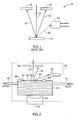
- FIG. 1 is a generalized diagram showing a longitudinal cross-section of the sample area of a prior art SEM 10.
- a primary electron beam 12 travels through a vacuum path to reach a sample 14. It strikes the sample 14 to form a stream of backscattered electrons 16, which strike a backscattered electron detector 18.
- secondary electrons 20 emitted by the sample are accelerated towards a secondary electron detector 22.
- the mean free path of an electron through the atmosphere is very small and thus the entire electron path, from an emitter via a sample to a detector, is in a vacuum, making it impossible to study wet samples or in-vivo processes.
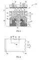
- FIG. 2 is a generalized diagram showing a longitudinal cross-section of a scanning electron microscope according to a first aspect of the present invention. Parts that are the same as those shown in the previous figure are given the same reference numerals and are not described again, except as necessary for an understanding of the present embodiment.
- a primary electron beam 12 travels through a vacuum chamber 30 towards a sample 32 which is placed within a chamber 34. Sealed within the chamber 34 is an atmosphere suitable for the retention of wet and living tissue, in which atmosphere in-vivo processes are able to take place.
- the most suitable environment will comprise an aqueous medium.
- a barrier 36 In order to seal the chamber from the vacuum chamber, a barrier 36, typically a membrane, is stretched across an aperture defined by a ring 38.
- the ring 38 is designed to hold the membrane 36 at its ends in an airtight fashion as will be shown in greater detail in connection with Fig. 3 below.
- the sample 32 is preferably placed close up to the membrane 36 so that the electron beam does not have to travel through the atmosphere within the chamber in order to reach the sample.
- the sample 32 is in actual physical contact with the membrane and in the case of living tissue, may be grown on the membrane or attached thereto using known methods, as will be exemplified hereinbelow.
- the chamber 34 comprises a relief outlet 40, which will be discussed in detail in connection with Fig. 3 below. It further comprises an inlet 41 and outlet 42 for fluids that maintain the appropriate conditions for the specimen.
- a relief outlet 40 which will be discussed in detail in connection with Fig. 3 below.
- It further comprises an inlet 41 and outlet 42 for fluids that maintain the appropriate conditions for the specimen.
- the inlet 41 and outlet 42 it is possible to utilize the inlet 41 and outlet 42 to change the chemical environment of the specimen being studied. This feature is particularly useful in the study of drugs, where it is possible to watch the dynamic reaction of a cell as the concentration of a given drug is changed.
- the membrane 36 may be a foil or a film and should preferably be able to withstand pressure gradients of up to one atmosphere whilst at the same time being transparent to an electron beam.
- a layer of polyimide substantially 1500 ⁇ thick is used as it can withstand the pressure gradient and is transparent to electron beams having energies in the region of 3keV and above.
- Thinner membranes are transparent to 2keV. More generally the thicknesses may lie within a range of 200 - 5000 ⁇ in order to withstand the necessary pressure gradient and at the same time be transparent to electrons at the beam energies available.
- Preferred materials are polyimide, for example of molecular formula C 12 H 12 N 2 0, polyamide, polyamide-imide, polyethylene, polypyrrole and additional conducting polymers, parlodion, collodion, silicon dioxide, silicon monoxide, carbon and trademarked materials including KaptonTM, FormVarTM, VinylecTM, PioloformTM and ButVarTM.
- a membrane composed of polyimide as described above allows for the passage of the primary beam and the resulting backscattered electrons 16.
- SEs Secondary electrons
- Typical materials include lithium fluoride.
- the SEs are detected by the SE detector 22 and thus serve to enhance the overall signal.
- the diameter of the exposed area of the membrane 36 within the aperture is substantially 1 - 3mm.
- the membrane is typically supported on a grid, each opening within the grid having a maximum diameter of substantially 0.1mm.
- the grid enhances the ability of the membrane to withstand a pressure gradient.
- the grid is schematically shown in Fig. 3 .
- the membrane preferably permits the maintenance of normal atmospheric conditions within the chamber 34, and thus permits the inspection of a range of samples that includes living cells, organelles or parts thereof, and proteins. It further allows the inspection of surfactants, colloids, oil particles, emulsions, and polymeric or micellar solutions.
- the chamber can, for example, be used to examine dynamic properties of drugs, such as swelling, dissolution and disintegration and even the resistance of cells to certain drugs.
- the chamber may be used for investigating the wetting and drying of wool, cotton and synthetic fibers.
- Other fields to which the invention is applicable may include petroleum, food, geology, microelectronics, paper coating and materials science.
- the chamber 34 itself can be filled with a gas or a liquid as desired and the samples can be monitored at the molecular level due to the nanometer range resolution of the electron beam.
- the resolution loss due to the membrane is negligible since there are very few scattering events which occur therein.
- a pressure relief device preferably comprising a spring 43 and an additional membrane 44, may be provided in the chamber to prevent the membrane 36 from bursting.
- the chamber 34 in accordance with embodiments of the present invention may be incorporated into standard SEMs, as discussed below in respect of Fig. 3 .
- the chamber 34 is compatible with standard specimen holders or specimen mounts.
- the specimen holder is designed according to the dimensions of standard commercial specimen holders so that it can be incorporated with ease into the specimen chamber, that is, the enclosure of the microscope for placement of the specimen holder.
- the chamber has been described as containing atmospheric pressure, this is not necessary for all samples and in certain cases lower pressures may be found to be suitable, hence reducing the pressure gradient across the membrane 36.
- a difficulty in using an electron beam to observe a living cell or an in-vivo process is that the electron beam itself damages the sample.
- Peak damage to DNA for example, occurs at 4keV.
- the choice of 3keV / 1500 ⁇ polyimide membrane is safely below the peak damage level.
- the damage level can further be optimized by finding an energy level which minimizes damage to the individual sample.
- a chamber 50 preferably of a size which fits into a conventional sample holder, comprises a sample holding assembly 51, which in turn comprises a body member 52 enclosing a sample region 54 having an open surface 55.
- the body member 52 is a standard SEM specimen mount.
- the sample region is enclosed by a membrane 56 of the type described above which is fitted over the exposed side of the sample region 54.
- a grid 59 is situated above the membrane and separated therefrom by a spacer 57.
- a closing member 58 fits over the body member 52 in such a way as to grip the membrane 56 around its edges.
- the closing member is attached to the body via threaded screws 62 which fit into corresponding holes in the enclosing members 58, which holes are continuous with threaded holes 60 in the body member 52.
- an O-ring seal 66 is fitted in the body member 52 around the sample region 54.
- a sample 64 is shown in close proximity with the membrane 56. Preferably, it should be either in actual contact with the membrane or within nanometers thereof so that the electron beam does not have to travel through any significant quantity of atmosphere.
- the assembly 68 comprises a stem 70 enclosing a channel 72.
- Channel 72 connects the sample region 54 with a further opening 74 at the far end of the stem 70.
- a sliding cylindrical closing member 76 comprising an upper part 77 which fits over a lower part 79 to press it inwardly against a second O-ring seal 78.
- the closing member 76 is preferably used to seal the opening 74 only after the sample region itself has been sealed, thus allowing a path for the excess fluid of the sample-holding assembly 51.
- Inserts 73 allow for insertion into a sample holder (not shown).
- a chamber 80 is produced as part of a light guide 82.
- a membrane 84 held by closing member 86, seals the chamber 80 from the vacuum.
- a reflective coating 90 preferably coats one end of the light guide 82, the other end leading in the direction of arrow 92 to a photomultiplier tube (not shown).
- a sample 94 is marked with an electro-luminescent (fluorescent) marker which is excited by the electron beam. The light is deflected in the direction of arrow 92 to be amplified by the photomultiplier tube (not shown).
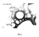
- Fig. 5 is an electron micrograph showing a wet specimen inspection using the embodiment shown Fig. 3 .
- the sample is an oil-in-water emulsion as used in a previous experiment to demonstrate ESEM contrast, described by Matthews (Proceedings of the Institute of Physics, EMAG99, page 95, Sheffield, 1999).
- the electron micrograph was taken with a JEOL 8400 SEM having low resolution, and a scale marker is shown.
- the resolution obtained using a membrane in accordance with the present invention is virtually the same as the resolution level achieved using the SEM in the conventional manner without a membrane. Good contrast is obtained and the overall results are sufficient for wet specimen inspection.
- a technology for imaging wet samples including but not limited to viable unfixed cells should deliver the following capabilities:
- the current invention is based on a Scanning Electron Microscope, which we modify to meet the specifications outlined above.
- sample preparation does not require coating, and allows working with living cells.
- fixation, de-hydration or coating drastically shortens and simplifies sample preparation procedures compared to conventional SEM, and significantly enhances the quality of the results.
- sample preparation procedure is suitable for labeling extracellular cell components, like the extracellular portion of membrane proteins. Other labeling techniques including labeling of intracellular cell components, are described in the examples section below. Labeling cells is done by the regular immunolabeling procedures.
- the current invention also solves the low throughput of laboratory SEMs. It utilizes for biological samples the SEM automation developed for the semiconductors industry for wafer-inspection. This idea of utilizing in biology the SEM automation developed for wafer-inspection is described at length in copending PCT application, entitled “Method of identification and quantification of biological molecules and apparatus therefore” ( PCT/IL01/00764 ) There, the samples are dry, allowing for straightforward usage of a Wafer Inspection Scanning Electron Microscope (WISEM) or WISEM-like microscope.
- WISEM Wafer Inspection Scanning Electron Microscope
- the automation strategy is a set of guidelines describing the procedures to be used in an automated imaging of live cell samples with the WET SEM technology.
- the automation procedure will include: A 'cell chip' containing a large number of isolated chambers where each chamber contains a sample prepared for wet SEM imaging. Each such subdivision (isolated chamber) contains a partition membrane on which cell samples (which may be identical or different) are grown.
- Standard automated fluid control can be used in the preparation of the samples.
- the cell chip Once the cell chip is ready for imaging it can be taken to an automated optical imaging (or alternatively low magnification SEM scan) using standard optical microscopy or special setup, like optical fiber etc., integrated into the SEM.
- This scan will provide an overview image of the cells in each chamber, their position and any other information relevant for the experiment.
- the information on the cells in this scan will be detected automatically using specifically developed algorithms.
- the partition membrane is mounted on a metal grid for mechanical stability.
- the grid supplies a convenient, extremely stable reference for the coordinates of every image.
- the cell chip is transferred to the SEM chamber for the SEMart imaging. Alignment algorithms will be used to match between the coordinate systems of the optical microscope and the SEM.
- ROI regions of interest
- Such ROI can include a specific region within a cell where important biological activity takes place or a region that is related to a specific sublocalization in the cell or a region which provides a statistical representation of other regions in the cell.
- the gold colloids are to be imaged in each such region.
- Such ROI can have different size hence requiring different magnification of the SEM.
- SEM images are taken automatically. This includes automated positioning of the SEM stage, automated focus and astigmatic corrections, automated brightness and contrast.
- Images taken by the SEM may be analyzed automatically using image analysis algorithms. This includes identification, counting and comparison of the position and size of gold colloids observed.
- signals can also be measured in the SEM imaging. These include signals from cathodoluminescent markers (as exemplified hereinbelow) or X-ray emission from the sample which can provide analytical chemical analysis of the samples.
- the embodiment of the wet-CL apparatus may be based on existing CL detectors or may involve the development of novel collection geometries and configurations.
- Existing detectors are, for example, those that collect light from the upper half plane (above the sample).
- an ellipsoidal mirror is placed above the sample, with a small hole in it to allow the passage of the electron beam.
- Light is collected by the mirror and directed towards a window in the microscope, beyond which a photon detector is situated.
- Such a collection configuration can be obtained commercially, for example from Gatan (previously Oxford Instruments).
- the apparatus is made as follows:
- the sample chamber (made of stainless steel) is closed on the upper part by the partition membrane and on the bottom part by a small lens so that the membrane is located at the focal plane of the lens.
- the sample chamber is put inside a stage where a prism redirects the light coming out of the lens at 90 degrees (i.e. horiziontally).
- the stage also contains a lens, which is used to refocus the light at the entrance of an optical fiber.
- the optical fiber leads from the stage to a detector located outside the microscope.
- the detector used is single photon module detection system. For each photon detected, the output signal is a TTL signal (0-5V square signal).
- the output of the detector is connected to a computer card, which counts the number of TTL signals (photons) received.
- the computer card receives also several signals from the microscope: beginning of an image acquisition; beginning of a new frame; beginning of a new line. Using appropriate software specially designed, the image is reconstructed in real-time from the collected data.
- Figure 6 shows the Sample Chamber with the different component parts a-E assembled together. The individual parts are described in detail in Figure 7 A-E .
- Figure 7 (A-E) shows a first embodiment of an assembly used for the fluorescent experiments
- Part A containing on the side a hole of several millimeters in diameter (not shown) is put up side down on the table.
- Part B is put inside taking care to align screw holes of parts A and B.
- Two o-rings are inserted in part B.
- the membrane is put in place.
- the membrane is mounted on a plastic support of 0.1mm thickness.
- the diameter of the plastic support has to be chosen between the two diameters of the o-rings used.
- the hole of 3mm diameter was previously preformed in the middle of the plastic support, this is the region where the membrane is free.
- a TEM grid is stuck on one side (the external one) of the membrane, in its middle.
- Part C is then inserted. It is important that the horizontal canal is aligned with the side hole of part A.
- the 6 screws are inserted.
- the membrane, parts A, B and C are screwed together.
- the sample is then ready to be filled with water, or any other aqueous medium.
- the liquid medium is deposited inside the free space in the middle of part C (while it is still upside down).
- a thin pin (0.1 mm diameter) is inserted through the hole practiced on the sides of part A and C.
- the pin is inserted deep inside, until its extremity reaches the wet chamber.
- the other extremity of the pin goes outside.
- the last o-ring is put in its place in part C. (At this stage the o-ring cannot be put in place completely, because the pin is there, just below. This is normal and useful for the following steps).
- Part D (containing in the middle the lens to collimate the light - not shown) is put in the assembly.
- Part E The inner side of the lens is wet by the medium filling the chamber. Finally Part E is inserted.
- Part E When turning Part E inside the assembly, the part D (with the lens) is pressed progressively on the o-ring (of Part C). Since the o-ring is not completely in place because of the pin, it does not isolate yet the chamber from the outside.
- the volume of the wet chamber is decreased, thus the medium in excess can flow out below the o-ring, in close proximity to the pin. Usually, some droplets flow out from the canal in Part C.
- the o-ring is pressed enough, and the lens is correctly placed, the pin is slowly pulled out.
- the o-ring in part B is free to occupy all the space. It comes to its natural position where it is sealing the chamber. Thus, the chamber is finally completely sealed at that stage.
- This assembly Parts A to E
- Parts A to E is then turned to its normal position (up-side up) and inserted inside the microscope stage specially designed for it.
- Figure 8 shows a microscope stage suitable for use with the assembly.
- the top cavity of the stage (2) is the recess into which the Sample Chamber is inserted.
- a prism Just below it is a prism.
- the prism (1) is used to redirect the light in the direction of a hole.
- a lens (not shown) focuses the light at the entrance of an optical fiber.
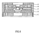
- FIG. 9 In order to get better light collection efficiency an alternative setup was designed where a direct coupling between the biological sample and a light guide is established.
- This alternative setup is shown in Fig 9 . It contains a vacuum tight chamber with a light going directly from the sample region to the single photon detector setup described above.
- the housing (1) is attached to the support (2), and a cover (3), using screws (6,7), within is situated a cavity disk (4), with the membrane (9), further connected to the light guide (5), sealed with the o-rings (8).
- the current invention is suitable for imaging cell components in either the intracellular or the extracellular parts of a cell.
- An alternative approach, which is suitable to living cells, is to insert the markers through a pinocytotic reaction.
- the cells can thereafter be fixed or observed while they are alive.
- the pinocytotic reaction preserves viability of the cell if it is performed under the appropriate conditions. It allows inserting molecules (fluorescent markers in most of the applications known in the art) or nanoscale particles (as particularly suitable for the present application). Some researchers have reported success in introducing beads on the micron scale inside cells also.
- Permeabilization and extraction procedures are suitable for fixed cells. Several procedures can be adopted, depending if the operator want to remove completely the cell membrane or just create some pores.
- Extraction and fixation means that the external membrane of the cell is first completely removed. Then, immediately after, the cell is fixed. This kind of procedure is good for visualizing structures in the cytoplasm, the nucleus or the cytoskeleton.
- Fixation and permeabilization means the cells are fixed first and further, the cell membrane is made permeable.
- Pinocytotic reaction is suitable for living cells.
- an agent such as the commercially available Influx (Molecular Probes I-14402 to introduce particles inside the cells.
- the Influx cell-loading technique is based on the osmotic lysis of pinocytotic vesicles. Briefly, compounds to be loaded are mixed at high concentration with a hypertonic medium, allowing the material to be carried into the cells via pinocytotic vesicles. The cells are then transferred to a hypotonic medium, which results in the release of trapped material from the pinocytotic vesicles within the cells, filling the cytosol with the compounds.
- Cell surface of living cells can be labeled with gold particles with low damage to the cells.
- An exemplary protocol developed for use in conjunction with the present invention utilizes streptavidin-biotin labeling methods as are known in the art. The idea is to incubate the cells with biotin that will attach to a certain percentage of the proteins on the cell surface. Then, the cells are incubated with streptavidin linked to gold particles that will attach to the biotin. The dosage of biotin for incubation must be carefully controlled, since too much biotin on the membrane protein may perturb their activity and induce cell death. Different studies have shown biotin can be used for cell tracking applications.
- Microcolumns A further development that will increase throughput is parallel inspection with microcolumns.
- the microcolumns are miniature scanning electron microscopes that are produced by integrated silicon processes. Due to their size, the microcolumns can operate in parallel; considerably reducing the scanning time and the bulkiness of a SEM based system. Further details of the microcolumns are given in Feinerman and Crewe "Miniature Electron Optics", Advances in Imaging and Electron Physics, Vol. 102, 187 (1998 ) as well as U.S. Patent No. 5,122,663 . This idea of utilizing microcolumns-based electron microscopes in biological applications is described at length in the copending PCT application, entitled “Method of identification and quantification of biological molecules and apparatus therefore” ( PCT/IL01/00764 ).
- the polyimide partition membranes are first coated with fibronectin (0.1 mg/ml) for 15 minutes. After washing with PBS and culture medium, cells are plated in the usual ways at concentrations of 800-1500 cells in 12-15 ⁇ l per chamber. After 24 hours cells are ready for manipulation/labeling. Most cell types can grow on the partition membrane itself without the support of an additional matrix like fibronectin, but under such conditions they would be more likely to be washed off during the extensive washing procedures. The viability of the cells is not affected by any of these procedures.
- the current invention is compatible with both adherent and non-adherent cells (as exemplified hereinbelow).
- non-adherent cells lymphocytes for example
- cells are first labeled in suspension, and then allowed to adhere for 30 minutes onto a partition membrane pre-treated with 0.4% poly-lysine for 1-3 hours.
- One possible strategy against such damage is to include additives to the medium of the cells that would absorb free radicals produced by the radiation, thereby minimizing the radiation damage to the cells.
- Any known compounds suitable for radical scavenging may be used as long as it is non-toxic to the cells.
- One exemplary candidate for such an additive is sucrose, which has been identified as a free radicals absorber. This solution is only possible with the current invention since conventional electron beam technology does not work in a wet environment.
- Labeling cells is done by the regular immunolabeling procedures. Cells were washed, and optionally fixed by 2% paraformaldehyde for 7 minutes. Following blocking with the appropriate serum, cells were incubated with a specific mono or polyclonal antibody for 1 hour. After washing, the samples are incubated with a second antibody that recognizes the first specific antibody. This second antibody is linked to a 5, 10, 20 or 40 nm gold cluster. The gold labeling may then be further amplified by silver enhancement, using conditions carefully calibrated for each colloid.
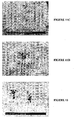
- Cells were fixed with 2% paraformaldehyde and labeled with anti FGF receptor monoclonal antibody (on C2C12 myoblasts) or anti-EGF monoclonal antibody (A431 cells) followed by anti mouse IgG linked to 20 nm-diameter gold colloids.
- the cells were fixed, and silver enhancement was used to increase the size of the labeling particles.
- An XL30 ESEM was used for imaging and the cells were examined with the backscattered electrons (BSE) mode.
- the FGF receptor gold labeling can be seen as bright spots on both cells shown in Figure 10A .
- the EGF receptors are visible on the A431 cells of Figures 10B-D .
- the fuzziness of the labeling around the nucleus area is the result of topographic differences between the gold particles.
- Gold labeling close to the partition membrane is clear and in focus, while the more distal labeling beyond and around the nucleus is fuzzy.
- the fuzziness of the labels in the region of the nucleus is evidence for the fact that the labels in this region are further away from the partition membrane. This fuzziness actually provides a tool for the determination of the distance of the labels from the plane of the partition membrane hence providing three-dimensional information. Using image analysis algorithms that are capable of deconvoluting the effect of the additional medium between the partition membrane and the labels can provide a rather accurate estimation of this distance.
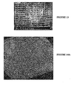
- Live C2C12 mouse myoblasts Cells were plated on fibronectin in their normal culture medium. After 24 hours the cells were examined with the BSE mode.
- the live C2C12 cells ( Figure 11 A-D ) and CHO cells ( Figure 12 ) show clearly the outline of the cell and its nucleolus as well as some sub-nuclei organelles.
- FIG. 10A shows in and out of focus gold labeling resulting from topographic differences between the gold particles as previously seen in the FGF receptor labeling of fixed C2C12 ( Fig. 10A ), and EGF receptor labeling of A431 cells ( Figs. 10B-D ).
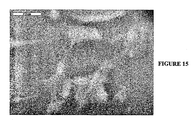
- the cells surface proteins were biotinylated and linked to Steptavidin attached to 40nm gold particles, as shown in Figure 15 .
Landscapes
- Chemical & Material Sciences (AREA)
- Analytical Chemistry (AREA)
- Analysing Materials By The Use Of Radiation (AREA)
- Sampling And Sample Adjustment (AREA)
- Investigating Or Analysing Biological Materials (AREA)
Claims (14)
- Procédé pour effectuer une microscopie électronique à balayage comprenant les étapes consistant à :délivrer un faisceau d'électrons (12) sur la région d'un spécimen (30) ;placer un spécimen (32, 64, 94) dans un assemblage d'enceinte de spécimen (34, 54, 80) ayant une ouverture et définissant un volume de placement de spécimen enclos scellé au niveau de ladite ouverture par un couvercle perméable au faisceau d'électrons, imperméable aux liquides, insensible au vide (36, 56, 84) ;placer ledit assemblage d'enceinte de spécimen dans ledit faisceau d'électrons (12) ; etdétecter des électrons rétrodiffusés (16) issus de l'interaction dudit faisceau d'électrons avec ledit spécimen (34, 64, 94).
- Procédé pour effectuer une microscopie électronique à balayage selon la revendication 1, comprenant l'étape consistant à :analyser les résultats des interactions dudit faisceau d'électrons avec ledit spécimen (34, 64, 94).
- Procédé pour effectuer une microscopie électronique à balayage selon la revendication 2, dans lequel l'analyse desdits résultats des interactions dudit faisceau d'électrons avec ledit spécimen (34, 64, 94) utilise des rayons X.
- Procédé pour effectuer une microscopie électronique à balayage selon la revendication 2, dans lequel l'analyse desdits résultats des interactions dudit faisceau d'électrons avec ledit spécimen (34, 64, 94) utilise de la lumière.
- Procédé pour effectuer une microscopie électronique à balayage selon la revendication 2, dans lequel l'analyse desdits résultats des interactions dudit faisceau d'électrons avec ledit spécimen (34, 64, 94) utilise des électrons.
- Assemblage de microscope électronique à balayage pour effectuer une microscopie électronique à balayage selon le procédé de la revendication 1, l'assemblage comprenant :un microscope électronique à balayage délivrant un faisceau d'électrons (12) sur la région d'un spécimen (30) ; etun assemblage d'enceinte de spécimen (34, 54, 80) disposé dans la région d'un spécimen (30) et définissant un volume de placement de spécimen enclos, l'assemblage d'enceinte de spécimen (34, 54, 80) comprenant une ouverture et un couvercle perméable au faisceau d'électrons, imperméable aux liquides, insensible au vide (36, 56, 84) scellant ledit volume de placement de spécimen au niveau de ladite ouverture par rapport à un volume situé hors dudit assemblage d'enceinte de spécimen, dans lequel le microscope électronique à balayage comprend un détecteur d'électrons (22) agencé pour détecter des électrons rétrodiffusés (16) issus de l'interaction dudit faisceau d'électrons (12) avec un spécimen (34, 64, 94) situé dans ledit assemblage d'enceinte de spécimen (34, 54, 80).
- Assemblage de microscope électronique à balayage selon la revendication 6, dans lequel ledit couvercle est formé d'un matériau sélectionné dans le groupe constitué de : polyimide, polyamide, polyamide-imide, polyéthylène, polypyrrole, PARLODION, COLLODION, KAPTON, FORMVAR, VINYLEC, BUTVAR, PIOLOFORM, dioxyde de silicium, monoxyde de silicium et de carbone.
- Assemblage de microscope électronique à balayage selon la revendication 6 ou la revendication 7, et comprenant en outre un support mécanique muni d'une ouverture (59) pour ledit couvercle (36, 56, 84) qui définit des ouvertures ayant un diamètre maximum sensiblement égal à 0,1 mm.
- Assemblage de microscope électronique à balayage selon l'une quelconque des revendications 6 à 8, et dans lequel un spécimen (32, 64, 94) est engagé au niveau dudit couvercle (36, 56, 84).
- Assemblage de microscope électronique à balayage selon l'une quelconque des revendications 6 à 9, et dans lequel ledit couvercle (36, 56, 84) peut supporter une différence de pression d'une atmosphère.
- Assemblage de microscope électronique à balayage selon l'une quelconque des revendications 6 à 10, et dans lequel ladite ouverture a un diamètre compris dans une plage s'étendant de 0,1 à 4 mm.
- Assemblage de microscope électronique à balayage selon l'une quelconque des revendications 6 à 11, et dans lequel ledit couvercle (36, 56, 84) est généralement perméable aux électrons ayant des énergies supérieures à 2 KeV.
- Assemblage de microscope électronique à balayage selon l'une quelconque des revendications 6 à 12, et comprenant en outre un dispositif de limitation de pression (43, 44, 68) communicant avec ledit assemblage d'enceinte de spécimen (34, 54, 94).
- Assemblage de microscope électronique à balayage selon l'une quelconque des revendications 6 à 13, et comprenant en outre un collecteur de lumière utilisé pour collecter la lumière générée par une interaction entre des électrons et un spécimen (32, 64, 94) à un emplacement au sein dudit assemblage d'enceinte de spécimen enclos (34, 54, 80).
Applications Claiming Priority (5)
| Application Number | Priority Date | Filing Date | Title |
|---|---|---|---|
| US25087900P | 2000-12-01 | 2000-12-01 | |
| US250879P | 2000-12-01 | ||
| US30645801P | 2001-07-20 | 2001-07-20 | |
| US306458P | 2001-07-20 | ||
| PCT/IL2001/001108 WO2002045125A1 (fr) | 2000-12-01 | 2001-11-30 | Dispositif et methode d'analyse d'echantillons dans un environnement non expose a une depression au moyen d'un microscope electronique a balayage |
Publications (3)
| Publication Number | Publication Date |
|---|---|
| EP1340241A1 EP1340241A1 (fr) | 2003-09-03 |
| EP1340241A4 EP1340241A4 (fr) | 2009-01-14 |
| EP1340241B1 true EP1340241B1 (fr) | 2011-05-18 |
Family
ID=26941209
Family Applications (1)
| Application Number | Title | Priority Date | Filing Date |
|---|---|---|---|
| EP01998987A Expired - Lifetime EP1340241B1 (fr) | 2000-12-01 | 2001-11-30 | Dispositif et methode d'analyse d'echantillons dans un environnement non expose a une depression au moyen d'un microscope electronique a balayage |
Country Status (10)
| Country | Link |
|---|---|
| US (3) | US6992300B2 (fr) |
| EP (1) | EP1340241B1 (fr) |
| JP (2) | JP4153303B2 (fr) |
| CN (1) | CN1511332A (fr) |
| AT (1) | ATE510298T1 (fr) |
| AU (2) | AU2002221019B2 (fr) |
| CA (1) | CA2436237A1 (fr) |
| CZ (1) | CZ20031455A3 (fr) |
| IL (1) | IL156027A0 (fr) |
| WO (1) | WO2002045125A1 (fr) |
Families Citing this family (141)
| Publication number | Priority date | Publication date | Assignee | Title |
|---|---|---|---|---|
| GB2367686B (en) * | 2000-08-10 | 2002-12-11 | Leo Electron Microscopy Ltd | Improvements in or relating to particle detectors |
| AU2003231893A1 (en) | 2002-06-05 | 2003-12-22 | Quantomix Ltd. | A sample enclosure for a scanning electron microscope and methods of use thereof |
| IL150056A0 (en) * | 2002-06-05 | 2002-12-01 | Yeda Res & Dev | Low-pressure chamber for scanning electron microscopy in a wet environment |
| US11243494B2 (en) | 2002-07-31 | 2022-02-08 | Abs Global, Inc. | Multiple laminar flow-based particle and cellular separation with laser steering |
| US20070125947A1 (en) * | 2003-02-20 | 2007-06-07 | David Sprinzak | Sample enclosure for a scanning electron microscope and methods of use thereof |
| US20050017173A1 (en) * | 2003-07-15 | 2005-01-27 | Nalin Kumar | Individually addressable nanoelectrode array |
| US7274447B2 (en) * | 2004-06-21 | 2007-09-25 | Swce | Material porosity pressure impulse testing system |
| US20060144778A1 (en) * | 2004-07-29 | 2006-07-06 | Grunthaner Frank J | Low stress, ultra-thin, uniform membrane, methods of fabricating same and incorporation into detection devices |
| US7626179B2 (en) * | 2005-09-30 | 2009-12-01 | Virgin Island Microsystems, Inc. | Electron beam induced resonance |
| US7791290B2 (en) | 2005-09-30 | 2010-09-07 | Virgin Islands Microsystems, Inc. | Ultra-small resonating charged particle beam modulator |
| US7586097B2 (en) | 2006-01-05 | 2009-09-08 | Virgin Islands Microsystems, Inc. | Switching micro-resonant structures using at least one director |
| EP1794772A2 (fr) * | 2004-08-26 | 2007-06-13 | Quantomix Ltd. | Conteneur d'echantillons pour inspection d'echantillons et procedes d'utilisation associes |
| NL1027025C2 (nl) | 2004-09-13 | 2006-03-14 | Univ Delft Tech | Microreactor voor een transmissie elektronenmicroscoop en verwarmingselement en werkwijze voor vervaardiging daarvan. |
| US7381970B2 (en) * | 2005-01-31 | 2008-06-03 | Summer Schneider | Specimen stage for charged-particle scanning microscopy |
| US20060172315A1 (en) * | 2005-02-01 | 2006-08-03 | Anderson Amy L | Methods for staining cells for identification and sorting |
| CN100511568C (zh) * | 2005-05-09 | 2009-07-08 | 东捷科技股份有限公司 | 在真空或低压环境中操作高压腔室且供观测的方法及装置 |
| TWI277734B (en) * | 2005-10-26 | 2007-04-01 | Li Bing Huan | Method for observing living bodies using an electron microscopy |
| TWI275118B (en) * | 2005-12-09 | 2007-03-01 | Li Bing Huan | Sample box of electron microscope for observing a general sample/live cell |
| JP2007163447A (ja) * | 2005-12-09 | 2007-06-28 | Lee Bing Huan | 電子顕微鏡用の超薄液体制御板 |
| EP1982346A4 (fr) * | 2006-02-02 | 2014-05-07 | Cebt Co Ltd | Dispositif permettant de maintenir des degrés de vide différents dans une colonne électronique |
| US7443358B2 (en) | 2006-02-28 | 2008-10-28 | Virgin Island Microsystems, Inc. | Integrated filter in antenna-based detector |
| US7646991B2 (en) | 2006-04-26 | 2010-01-12 | Virgin Island Microsystems, Inc. | Selectable frequency EMR emitter |
| US7876793B2 (en) | 2006-04-26 | 2011-01-25 | Virgin Islands Microsystems, Inc. | Micro free electron laser (FEL) |
| JP2007294365A (ja) * | 2006-04-27 | 2007-11-08 | Jeol Ltd | 試料検査方法、試料保持体、及び試料検査装置並びに試料検査システム |
| JP2007292702A (ja) * | 2006-04-27 | 2007-11-08 | Jeol Ltd | 試料検査装置及び試料検査方法並びに試料検査システム |
| US7728702B2 (en) | 2006-05-05 | 2010-06-01 | Virgin Islands Microsystems, Inc. | Shielding of integrated circuit package with high-permeability magnetic material |
| US7718977B2 (en) | 2006-05-05 | 2010-05-18 | Virgin Island Microsystems, Inc. | Stray charged particle removal device |
| US8188431B2 (en) | 2006-05-05 | 2012-05-29 | Jonathan Gorrell | Integration of vacuum microelectronic device with integrated circuit |
| US7436177B2 (en) * | 2006-05-05 | 2008-10-14 | Virgin Islands Microsystems, Inc. | SEM test apparatus |
| US7732786B2 (en) | 2006-05-05 | 2010-06-08 | Virgin Islands Microsystems, Inc. | Coupling energy in a plasmon wave to an electron beam |
| US7359589B2 (en) | 2006-05-05 | 2008-04-15 | Virgin Islands Microsystems, Inc. | Coupling electromagnetic wave through microcircuit |
| US7656094B2 (en) * | 2006-05-05 | 2010-02-02 | Virgin Islands Microsystems, Inc. | Electron accelerator for ultra-small resonant structures |
| US7746532B2 (en) | 2006-05-05 | 2010-06-29 | Virgin Island Microsystems, Inc. | Electro-optical switching system and method |
| US7728397B2 (en) | 2006-05-05 | 2010-06-01 | Virgin Islands Microsystems, Inc. | Coupled nano-resonating energy emitting structures |
| US7710040B2 (en) | 2006-05-05 | 2010-05-04 | Virgin Islands Microsystems, Inc. | Single layer construction for ultra small devices |
| US7723698B2 (en) | 2006-05-05 | 2010-05-25 | Virgin Islands Microsystems, Inc. | Top metal layer shield for ultra-small resonant structures |
| US7986113B2 (en) | 2006-05-05 | 2011-07-26 | Virgin Islands Microsystems, Inc. | Selectable frequency light emitter |
| US7741934B2 (en) | 2006-05-05 | 2010-06-22 | Virgin Islands Microsystems, Inc. | Coupling a signal through a window |
| US7679067B2 (en) | 2006-05-26 | 2010-03-16 | Virgin Island Microsystems, Inc. | Receiver array using shared electron beam |
| US7655934B2 (en) | 2006-06-28 | 2010-02-02 | Virgin Island Microsystems, Inc. | Data on light bulb |
| JP5084188B2 (ja) * | 2006-07-04 | 2012-11-28 | 日本電子株式会社 | 試料保持体、試料検査方法及び試料検査装置並びに試料検査システム |
| US7450794B2 (en) | 2006-09-19 | 2008-11-11 | Virgin Islands Microsystems, Inc. | Microcircuit using electromagnetic wave routing |
| JP4850654B2 (ja) * | 2006-10-23 | 2012-01-11 | 株式会社日立ハイテクノロジーズ | 荷電粒子線装置および荷電粒子線装置用試料保持装置 |
| WO2008050321A2 (fr) | 2006-10-24 | 2008-05-02 | B-Nano Ltd. | Interface, procédé pour observer un objet dans un environnement non vide et microscope électronique à balayage |
| JP5002251B2 (ja) | 2006-12-06 | 2012-08-15 | 日本電子株式会社 | 試料検査方法及び試料検査装置 |
| TWI330380B (en) * | 2006-12-07 | 2010-09-11 | Nat Univ Tsing Hua | A specimen kit for electron microscope and its fabrication process |
| JP2008153086A (ja) * | 2006-12-19 | 2008-07-03 | Jeol Ltd | 試料検査装置及び試料検査方法並びに試料検査システム |
| EP2365321B1 (fr) | 2006-12-19 | 2013-10-02 | JEOL Ltd. | Appareil d'inspection d'échantillon, procédé d'inspection d'échantillon et système d'inspection d'échantillon |
| US7659513B2 (en) | 2006-12-20 | 2010-02-09 | Virgin Islands Microsystems, Inc. | Low terahertz source and detector |
| JP5318364B2 (ja) | 2007-01-31 | 2013-10-16 | 日本電子株式会社 | 試料保持体、試料検査装置及び試料検査方法、並びに試料保持体の製造方法 |
| EP1953793B1 (fr) | 2007-01-31 | 2012-05-16 | JEOL Ltd. | Porte-spécimens, appareil d'inspection de spécimens, procédé d'inspection de spécimens et procédé pour la fabrication de porte-spécimens |
| JP2008210715A (ja) * | 2007-02-27 | 2008-09-11 | Ebara Corp | 荷電粒子線装置及びこれを用いた試料表面観察方法 |
| EP2130086A4 (fr) | 2007-03-02 | 2012-03-14 | Protochips Inc | Supports à membrane avec fonctions de renforcement |
| US7990336B2 (en) | 2007-06-19 | 2011-08-02 | Virgin Islands Microsystems, Inc. | Microwave coupled excitation of solid state resonant arrays |
| US9134307B2 (en) | 2007-07-11 | 2015-09-15 | X-Body, Inc. | Method for determining ion channel modulating properties of a test reagent |
| WO2009009718A1 (fr) | 2007-07-11 | 2009-01-15 | Sru Biosystems, Inc. | Procédés d'identification de modulateurs de canaux ioniques |
| US7791053B2 (en) | 2007-10-10 | 2010-09-07 | Virgin Islands Microsystems, Inc. | Depressed anode with plasmon-enabled devices such as ultra-small resonant structures |
| EP2565900B1 (fr) | 2007-11-13 | 2016-02-03 | Carl Zeiss Microscopy Limited | Dispositif de faisceau et système comportant un système de faisceau à particules et microscope optique |
| JP5253800B2 (ja) * | 2007-12-26 | 2013-07-31 | 日本電子株式会社 | 試料保持体及び観察・検査方法並びに観察・検査装置 |
| JP5215701B2 (ja) | 2008-03-26 | 2013-06-19 | 日本電子株式会社 | 試料検査装置及び試料検査方法 |
| EP2105944A1 (fr) * | 2008-03-28 | 2009-09-30 | FEI Company | "Cellule environnementale" pour appareil optique à particules chargées |
| JP5314317B2 (ja) * | 2008-04-08 | 2013-10-16 | 日本電子株式会社 | 検査方法及び試液 |
| JP2010002300A (ja) | 2008-06-20 | 2010-01-07 | Jeol Ltd | 試料保持体、試料検査装置及び試料検査方法 |
| WO2010001399A1 (fr) * | 2008-07-03 | 2010-01-07 | B-Nano | Microscope électronique à balayage, interface et procédé d’observation d’un objet dans un environnement non vide |
| US8981294B2 (en) | 2008-07-03 | 2015-03-17 | B-Nano Ltd. | Scanning electron microscope, an interface and a method for observing an object within a non-vacuum environment |
| JP2010027488A (ja) | 2008-07-23 | 2010-02-04 | Jeol Ltd | 試料保持体、試料検査装置及び試料検査方法 |
| US8492716B2 (en) * | 2008-09-28 | 2013-07-23 | B-Nano Ltd. | Vacuumed device and a scanning electron microscope |
| JP5205234B2 (ja) * | 2008-12-02 | 2013-06-05 | 株式会社日立ハイテクノロジーズ | 微小試料採取装置,検査解析システム、および検査解析方法 |
| US8059271B2 (en) | 2009-02-04 | 2011-11-15 | The United States Of America As Represented By The Secretary Of The Army | Reusable sample holding device permitting ready loading of very small wet samples |
| JP5124507B2 (ja) | 2009-02-16 | 2013-01-23 | 株式会社日立ハイテクノロジーズ | 電子線装置および電子線装置用試料保持装置 |
| JP2010230417A (ja) | 2009-03-26 | 2010-10-14 | Jeol Ltd | 試料の検査装置及び検査方法 |
| US8087309B2 (en) | 2009-05-22 | 2012-01-03 | Sion Power Corporation | Hermetic sample holder and method for performing microanalysis under controlled atmosphere environment |
| NL2004888A (en) * | 2009-06-29 | 2010-12-30 | Asml Netherlands Bv | Deposition method and apparatus. |
| CA2768873A1 (fr) * | 2009-07-23 | 2011-01-27 | Insight Nanofluidics Inc. | Cellule nanofluidique |
| DE112010005188B4 (de) * | 2010-01-27 | 2016-04-07 | Hitachi High-Technologies Corp. | Vorrichtung zum Bestrahlen mit geladenen Teilchen |
| JP2011243483A (ja) | 2010-05-20 | 2011-12-01 | Jeol Ltd | 試料保持体、検査装置、及び検査方法 |
| JP5065516B2 (ja) * | 2010-08-04 | 2012-11-07 | エフ イー アイ カンパニ | 薄い電子検出器における後方散乱の減少 |
| JP5218503B2 (ja) * | 2010-09-01 | 2013-06-26 | コニカミノルタビジネステクノロジーズ株式会社 | 光走査装置および画像形成装置 |
| WO2012041721A1 (fr) | 2010-10-01 | 2012-04-05 | Attolight Sa | Déconvolution d'images cathodoluminescentes à découpage temporel |
| US10908066B2 (en) | 2010-11-16 | 2021-02-02 | 1087 Systems, Inc. | Use of vibrational spectroscopy for microfluidic liquid measurement |
| US20120190137A1 (en) * | 2011-01-24 | 2012-07-26 | Sumitomo Electric Industries, Ltd. | Cross section observation method |
| US10505234B2 (en) | 2011-03-14 | 2019-12-10 | Battelle Memorial Institute | Battery cell and n situ battery electrode analysis method |
| US10598609B2 (en) * | 2011-03-14 | 2020-03-24 | Battelle Memorial Institute | Universal liquid sample device and process for high resolution transmission electron microscope imaging and multimodal analyses of liquid sample materials |
| US9274059B2 (en) | 2011-03-14 | 2016-03-01 | Battelle Memorial Institute | Microfluidic electrochemical device and process for chemical imaging and electrochemical analysis at the electrode-liquid interface in-situ |
| US8555710B2 (en) * | 2011-03-14 | 2013-10-15 | Battelle Memorial Institute | Systems and methods for analyzing liquids under vacuum |
| JP5699023B2 (ja) | 2011-04-11 | 2015-04-08 | 株式会社日立ハイテクノロジーズ | 荷電粒子線装置 |
| CN103493171B (zh) * | 2011-04-28 | 2016-02-17 | 株式会社日立高新技术 | 电子显微镜用试样保持装置以及电子显微镜装置 |
| EP3528276A3 (fr) | 2011-05-13 | 2019-09-04 | Fibics Incorporated | Procédé d'imagerie par microscopie |
| EP2732299A4 (fr) | 2011-07-15 | 2015-03-25 | Orbotech Ltd | Inspection électrique de dispositifs électroniques à l'aide de sondes à plasma induit par faisceau d'électrons |
| EP2734836A4 (fr) | 2011-07-21 | 2015-07-22 | Univ Columbia | Procédé de collecte et de traitement de données sur la diffraction d'électrons |
| JP5896708B2 (ja) | 2011-12-06 | 2016-03-30 | 株式会社日立ハイテクノロジーズ | 走査イオン顕微鏡および二次粒子制御方法 |
| JP5115997B1 (ja) * | 2011-12-27 | 2013-01-09 | 独立行政法人産業技術総合研究所 | 走査型電子顕微鏡像観察用の試料支持部材及び走査型電子顕微鏡像の観察方法 |
| JP2013187096A (ja) * | 2012-03-09 | 2013-09-19 | Hitachi Ltd | 電子顕微鏡の液体試料ホルダ及びその製造方法 |
| US8809783B2 (en) * | 2012-06-19 | 2014-08-19 | Rensselaer Polytechnic Institute | High spatial resolution non-contact temperature measurement |
| JP6002946B2 (ja) | 2012-07-23 | 2016-10-05 | 国立研究開発法人産業技術総合研究所 | 試料ホルダおよび電子顕微鏡像の観察方法 |
| JP5936484B2 (ja) | 2012-08-20 | 2016-06-22 | 株式会社日立ハイテクノロジーズ | 荷電粒子線装置及び試料観察方法 |
| JP5923412B2 (ja) | 2012-08-24 | 2016-05-24 | 株式会社日立ハイテクノロジーズ | 観察装置および光軸調整方法 |
| JP5930922B2 (ja) | 2012-09-14 | 2016-06-08 | 株式会社日立ハイテクノロジーズ | 荷電粒子線装置及び試料観察方法 |
| JP6207824B2 (ja) | 2012-10-01 | 2017-10-04 | 株式会社日立ハイテクノロジーズ | 荷電粒子線装置、隔膜の位置調整方法および隔膜位置調整ジグ |
| JP6051014B2 (ja) | 2012-10-29 | 2016-12-21 | 株式会社日立ハイテクノロジーズ | 試料格納用容器、荷電粒子線装置、及び画像取得方法 |
| JP6035602B2 (ja) * | 2012-11-21 | 2016-11-30 | 株式会社日立ハイテクノロジーズ | 荷電粒子線装置、試料台ユニット、及び試料観察方法 |
| US8872105B2 (en) * | 2013-02-19 | 2014-10-28 | Fei Company | In situ reactivation of fluorescence marker |
| EP2959287A4 (fr) | 2013-02-20 | 2016-10-19 | Nano Ltd B | Microscope électronique à balayage |
| KR102026936B1 (ko) * | 2013-03-26 | 2019-10-01 | 삼성디스플레이 주식회사 | 주사 전자 현미경을 이용한 검사 시스템 |
| JP6112553B2 (ja) | 2013-04-08 | 2017-04-12 | 国立研究開発法人産業技術総合研究所 | 観察システム及び観察方法 |
| DE112014001109B4 (de) * | 2013-04-12 | 2019-11-14 | Hitachi High-Technologies Corporation | Mit einem Strahl geladener Teilchen arbeitende Vorrichtung und Filterelement |
| US8961904B2 (en) | 2013-07-16 | 2015-02-24 | Premium Genetics (Uk) Ltd. | Microfluidic chip |
| DE102013012609B4 (de) * | 2013-07-26 | 2024-06-27 | Carl Zeiss Microscopy Gmbh | Optoelektronischer Detektor, insbesondere für hochauflösende Lichtrastermikroskope und Lichtrastermikroskop |
| DE112014003268B4 (de) | 2013-08-23 | 2018-05-30 | Hitachi High-Technologies Corporation | Membrananbringungselement, mit einem strahl geladener teilchen arbeitende vorrichtung, system, membrananbringungsverfahren sowie verfahren zum inspizieren der qualität |
| US9741526B2 (en) | 2013-09-06 | 2017-08-22 | Hitachi High-Technologies Corporation | Charged particle beam apparatus and sample image acquiring method |
| JP6364167B2 (ja) * | 2013-09-30 | 2018-07-25 | 株式会社日立ハイテクノロジーズ | 環境制御型荷電粒子観察システム |
| USD794816S1 (en) * | 2013-10-24 | 2017-08-15 | Hitachi High-Technologies Corporation | Sample holder for an electron microscope |
| US11796449B2 (en) | 2013-10-30 | 2023-10-24 | Abs Global, Inc. | Microfluidic system and method with focused energy apparatus |
| US10410338B2 (en) * | 2013-11-04 | 2019-09-10 | Kla-Tencor Corporation | Method and system for correlating optical images with scanning electron microscopy images |
| US9997331B1 (en) | 2014-01-27 | 2018-06-12 | Mochii, Inc. | Charged-particle beam microscopy |
| JP6047508B2 (ja) | 2014-01-27 | 2016-12-21 | 株式会社日立ハイテクノロジーズ | 荷電粒子線装置、試料画像取得方法、およびプログラム記録媒体 |
| US9564291B1 (en) * | 2014-01-27 | 2017-02-07 | Mochii, Inc. | Hybrid charged-particle beam and light beam microscopy |
| US20160032281A1 (en) * | 2014-07-31 | 2016-02-04 | Fei Company | Functionalized grids for locating and imaging biological specimens and methods of using the same |
| GB2537579A (en) * | 2014-11-07 | 2016-10-26 | Linkam Scient Instr Ltd | Microscopic sample preparation |
| TWI546841B (zh) | 2014-12-10 | 2016-08-21 | 財團法人工業技術研究院 | 具有載台的電子顯微鏡 |
| WO2016132222A2 (fr) | 2015-02-19 | 2016-08-25 | Premium Genetics (Uk) Ltd. | Système de mesure infrarouge à balayage |
| WO2017033219A1 (fr) | 2015-08-21 | 2017-03-02 | 株式会社 日立ハイテクノロジーズ | Unité de support d'observation pour microscope à particules chargées et procédé d'observation d'échantillon faisant intervenir ladite unité |
| TWI597481B (zh) * | 2015-12-22 | 2017-09-01 | 閤康生物科技股份有限公司 | 樣本收集元件及其製作方法 |
| TWI594288B (zh) * | 2016-03-14 | 2017-08-01 | 台灣電鏡儀器股份有限公司 | 電子顯微鏡 |
| CN106525845B (zh) * | 2016-10-11 | 2023-11-03 | 聚束科技(北京)有限公司 | 一种带电粒子束系统、光电联合探测系统及方法 |
| CN106783493B (zh) * | 2016-12-01 | 2018-07-10 | 聚束科技(北京)有限公司 | 一种真空气氛处理装置、样品观测系统及方法 |
| US11051390B2 (en) * | 2017-03-22 | 2021-06-29 | Japan Atomic Energy Agency | Functional membrane for ion beam transmission, beam line device and filter device each having the same, and method of adjusting filter device |
| WO2019226790A1 (fr) | 2018-05-23 | 2019-11-28 | Abs Global, Inc. | Systèmes et procédés de focalisation de particules dans des microcanaux |
| CN109187595B (zh) * | 2018-09-27 | 2021-05-11 | 南京宁智高新材料研究院有限公司 | 一种测量透射电镜中微气体束引起的局部等效压强的装置 |
| JP7189529B2 (ja) * | 2018-10-15 | 2022-12-14 | 国立大学法人 筑波大学 | 環境セルとその製造方法 |
| US11538659B2 (en) * | 2018-10-25 | 2022-12-27 | Hitachi High-Tech Corporation | Charged particle beam device, autofocus processing method of charged particle beam device, and detector |
| US10777379B1 (en) * | 2019-03-19 | 2020-09-15 | Hitachi High-Tech Corporation | Holder and charged particle beam apparatus |
| KR102198707B1 (ko) * | 2019-03-25 | 2021-01-05 | (주)코셈 | 착탈 가능한 컬럼을 구비하는 주사 전자 현미경 및, 이를 이용한 영상 획득 방법 |
| CN117413819A (zh) | 2019-04-18 | 2024-01-19 | 艾步思国际有限责任公司 | 用于连续添加冷冻保护剂的系统和工艺 |
| US11738312B2 (en) * | 2019-08-01 | 2023-08-29 | Government Of The United States Of America, As Represented By The Secretary Of Commerce | Multidimensional printer |
| US11628439B2 (en) | 2020-01-13 | 2023-04-18 | Abs Global, Inc. | Single-sheath microfluidic chip |
| NL2024861B1 (en) * | 2020-02-07 | 2021-09-13 | Univ Delft Tech | Method for recording and correlating light and charged particle microscopy images |
| US11410838B2 (en) | 2020-09-03 | 2022-08-09 | Thermo Finnigan Llc | Long life electron multiplier |
| CN112461807B (zh) * | 2020-11-26 | 2021-11-19 | 山西大学 | 碳量子点在靶向细胞核仁免洗成像中的应用 |
| DE102021101982A1 (de) | 2021-01-28 | 2022-07-28 | ebm-papst neo GmbH & Co. KG | Vorrichtung und Verfahren zur Erfassung einer Konzentration von vorbestimmten Partikeln anhand ihrer morphologischen Eigenschaften in Luft |
| CN114113182A (zh) * | 2021-10-22 | 2022-03-01 | 合肥国轩高科动力能源有限公司 | 一种用于扫描电镜拍摄硅基负极材料的定位处理方法 |
Family Cites Families (50)
| Publication number | Priority date | Publication date | Assignee | Title |
|---|---|---|---|---|
| FR1345670A (fr) * | 1962-10-25 | 1963-12-13 | Radiologie Cie Gle | Perfectionnements aux porte-échantillons liquides pour spectromètres à rayons chious vide |
| US3657596A (en) * | 1965-05-20 | 1972-04-18 | Westinghouse Electric Corp | Electron image device having target comprising porous region adjacent conductive layer and outer, denser region |
| US3378684A (en) * | 1965-06-16 | 1968-04-16 | Gen Electric | Fluid sample cell with means to keep constant pressure on the sample fluid |
| US4071766A (en) * | 1974-03-28 | 1978-01-31 | Mta Kozponti Kemiai Kutato Intezet | Micro-chamber for electron optical examinations particularly for the electron microscopic examination of biological objects |
| JPS5168585U (fr) * | 1974-11-26 | 1976-05-31 | ||
| US4115689A (en) * | 1977-07-06 | 1978-09-19 | Won Vann Y | Leveling device for forming X-ray specimen |
| US4308547A (en) * | 1978-04-13 | 1981-12-29 | Recognition Equipment Incorporated | Liquid drop emitter |
| DE2921151C2 (de) * | 1979-05-25 | 1982-12-02 | Ernst Leitz Wetzlar Gmbh, 6330 Wetzlar | Vorrichtung zum Nachweis von in einem Abtast-Elektronenstrahlmikroskop von einer Probe ausgehenden Rückstreuelektronen |
| AU534811B2 (en) * | 1979-07-03 | 1984-02-16 | Unisearch Limited | Atmospheric scanning electron microscope |
| US4448311A (en) * | 1983-01-24 | 1984-05-15 | Tech Ref, Inc. | Sample cell |
| JPS59168652A (ja) * | 1983-03-16 | 1984-09-22 | Hitachi Ltd | 素子修正方法及びその装置 |
| US4618938A (en) * | 1984-02-22 | 1986-10-21 | Kla Instruments Corporation | Method and apparatus for automatic wafer inspection |
| US4587666A (en) * | 1984-05-03 | 1986-05-06 | Angelo M. Torrisi | System and a method for mounting film to a sample holder for X-ray spectroscopic fluorescence analysis |
| US4720622A (en) * | 1985-03-11 | 1988-01-19 | Sanyo Electric Co., Ltd | Wall-mounted type cooking apparatus |
| US4705949A (en) * | 1985-11-25 | 1987-11-10 | The United States Of America As Represented By The Secretary Of Commerce | Method and apparatus relating to specimen cells for scanning electron microscopes |
| US4720633A (en) * | 1986-01-17 | 1988-01-19 | Electro-Scan Corporation | Scanning electron microscope for visualization of wet samples |
| JPH0687410B2 (ja) * | 1986-08-01 | 1994-11-02 | エレクトロ‐スキャン コーポレーション | 走査電子顕微鏡及び試料の表面を電子顕微鏡的に像形成する方法 |
| US4880976A (en) * | 1987-05-21 | 1989-11-14 | Electroscan Corporation | Secondary electron detector for use in a gaseous atmosphere |
| US5250808A (en) * | 1987-05-21 | 1993-10-05 | Electroscan Corporation | Integrated electron optical/differential pumping/imaging signal system for an environmental scanning electron microscope |
| JPH0614461B2 (ja) | 1987-05-22 | 1994-02-23 | 日本電子株式会社 | 電子顕微鏡におけるガス雰囲気試料ホルダ |
| US4929831A (en) * | 1988-12-08 | 1990-05-29 | The United States Of America As Represented By The Secretary Of The Navy | Electron beam apparatus for testing infrared detectors in a cryogenically shielded environment |
| US4912330A (en) * | 1988-12-27 | 1990-03-27 | United States Of America As Represented By The Secretary Of The Navy | Apparatus for X-ray testing long wave infrared radiation detectors |
| US4929041A (en) * | 1989-01-09 | 1990-05-29 | Johnston Pump/General Valve, Inc. | Cathodoluminescence system for use in a scanning electron microscope including means for controlling optical fiber aperture |
| US5103102A (en) * | 1989-02-24 | 1992-04-07 | Micrion Corporation | Localized vacuum apparatus and method |
| JP2794471B2 (ja) * | 1989-11-24 | 1998-09-03 | 日本電子テクニクス株式会社 | 電子顕微鏡 |
| US5866904A (en) * | 1990-10-12 | 1999-02-02 | Hitachi, Ltd. | Scanning electron microscope and method for dimension measuring by using the same |
| JP3148353B2 (ja) * | 1991-05-30 | 2001-03-19 | ケーエルエー・インストルメンツ・コーポレーション | 電子ビーム検査方法とそのシステム |
| US5470757A (en) * | 1991-06-25 | 1995-11-28 | Minnesota Mining And Manufacturing Company | Spectroscopic sample holder and method for using same |
| US5122663A (en) * | 1991-07-24 | 1992-06-16 | International Business Machine Corporation | Compact, integrated electron beam imaging system |
| US5323441A (en) * | 1992-12-15 | 1994-06-21 | Angelo M. Torrisi | Sample holder for spectroscopic analysis and method for mounting film to sample holder |
| JP2781320B2 (ja) | 1993-01-18 | 1998-07-30 | 株式会社蛋白工学研究所 | 電子顕微鏡等の試料ホルダ |
| US5326971A (en) * | 1993-05-17 | 1994-07-05 | Motorola, Inc. | Transmission electron microscope environmental specimen holder |
| US5412211A (en) * | 1993-07-30 | 1995-05-02 | Electroscan Corporation | Environmental scanning electron microscope |
| US5362964A (en) * | 1993-07-30 | 1994-11-08 | Electroscan Corporation | Environmental scanning electron microscope |
| US5644132A (en) * | 1994-06-20 | 1997-07-01 | Opan Technologies Ltd. | System for high resolution imaging and measurement of topographic and material features on a specimen |
| US5466940A (en) * | 1994-06-20 | 1995-11-14 | Opal Technologies Ltd. | Electron detector with high backscattered electron acceptance for particle beam apparatus |
| US6025592A (en) * | 1995-08-11 | 2000-02-15 | Philips Electronics North America | High temperature specimen stage and detector for an environmental scanning electron microscope |
| US5898261A (en) * | 1996-01-31 | 1999-04-27 | The United States Of America As Represented By The Secretary Of The Air Force | Fluid-cooled particle-beam transmission window |
| EP0865454B1 (fr) * | 1996-03-20 | 2001-01-03 | Celanese International Corporation | Addition d'amine permettant d'accroitre la production de paraformaldehyde |
| US5667791A (en) * | 1996-05-31 | 1997-09-16 | Thione International, Inc. | X-ray induced skin damage protective composition |
| JPH1064467A (ja) * | 1996-08-23 | 1998-03-06 | Toshiba Corp | 電子顕微鏡 |
| JP3500264B2 (ja) * | 1997-01-29 | 2004-02-23 | 株式会社日立製作所 | 試料分析装置 |
| US5859699A (en) * | 1997-02-07 | 1999-01-12 | Arcturus Engineering, Inc. | Laser capture microdissection analysis vessel |
| US5789748A (en) * | 1997-05-29 | 1998-08-04 | Stanford University | Low voltage electron beam system |
| US5945672A (en) * | 1998-01-29 | 1999-08-31 | Fei Company | Gaseous backscattered electron detector for an environmental scanning electron microscope |
| IL139743A0 (en) * | 1998-05-22 | 2002-02-10 | Euro Celtique Sa | Dissolution stage for an environmental scanning electron microscope |
| US6452177B1 (en) * | 1998-09-04 | 2002-09-17 | California Institute Of Technology | Atmospheric electron x-ray spectrometer |
| JP3610245B2 (ja) | 1998-10-27 | 2005-01-12 | 日本電子株式会社 | ガス雰囲気試料ホルダ |
| WO2002014830A2 (fr) | 2000-08-17 | 2002-02-21 | Yeda Research And Development Co. Ltd. | Methode d'identification et de quantification de molecules biologiques et appareil correspondant |
| JP2002273446A (ja) | 2001-03-19 | 2002-09-24 | Sanyo Electric Co Ltd | 汚水処理装置用電解槽 |
-
2001
- 2001-11-30 AU AU2002221019A patent/AU2002221019B2/en not_active Ceased
- 2001-11-30 EP EP01998987A patent/EP1340241B1/fr not_active Expired - Lifetime
- 2001-11-30 JP JP2002547196A patent/JP4153303B2/ja not_active Expired - Fee Related
- 2001-11-30 CA CA002436237A patent/CA2436237A1/fr not_active Abandoned
- 2001-11-30 CZ CZ20031455A patent/CZ20031455A3/cs unknown
- 2001-11-30 AT AT01998987T patent/ATE510298T1/de not_active IP Right Cessation
- 2001-11-30 IL IL15602701A patent/IL156027A0/xx active IP Right Grant
- 2001-11-30 AU AU2101902A patent/AU2101902A/xx active Pending
- 2001-11-30 CN CNA018199062A patent/CN1511332A/zh active Pending
- 2001-11-30 WO PCT/IL2001/001108 patent/WO2002045125A1/fr active Application Filing
-
2003
- 2003-05-27 US US10/448,313 patent/US6992300B2/en not_active Expired - Lifetime
-
2004
- 2004-05-06 US US10/841,769 patent/US6989542B2/en not_active Expired - Lifetime
-
2005
- 2005-08-19 US US11/207,611 patent/US7253418B2/en not_active Expired - Fee Related
-
2008
- 2008-04-03 JP JP2008097275A patent/JP2008171830A/ja active Pending
Also Published As
| Publication number | Publication date |
|---|---|
| CZ20031455A3 (cs) | 2003-10-15 |
| IL156027A0 (en) | 2003-12-23 |
| JP2004515049A (ja) | 2004-05-20 |
| ATE510298T1 (de) | 2011-06-15 |
| US20060033038A1 (en) | 2006-02-16 |
| JP4153303B2 (ja) | 2008-09-24 |
| US7253418B2 (en) | 2007-08-07 |
| AU2101902A (en) | 2002-06-11 |
| US6989542B2 (en) | 2006-01-24 |
| WO2002045125A1 (fr) | 2002-06-06 |
| CA2436237A1 (fr) | 2002-06-06 |
| US20040217297A1 (en) | 2004-11-04 |
| JP2008171830A (ja) | 2008-07-24 |
| EP1340241A4 (fr) | 2009-01-14 |
| AU2002221019B2 (en) | 2007-02-08 |
| CN1511332A (zh) | 2004-07-07 |
| US6992300B2 (en) | 2006-01-31 |
| US20040046120A1 (en) | 2004-03-11 |
| EP1340241A1 (fr) | 2003-09-03 |
Similar Documents
| Publication | Publication Date | Title |
|---|---|---|
| EP1340241B1 (fr) | Dispositif et methode d'analyse d'echantillons dans un environnement non expose a une depression au moyen d'un microscope electronique a balayage | |
| AU2002221019A1 (en) | Device and method for the examination of samples in a non-vacuum environment using a scanning electron microscope | |
| US7745802B2 (en) | Specimen holder, specimen inspection apparatus, specimen inspection method, and method of fabricating specimen holder | |
| EP2388575A1 (fr) | Support d'échantillons, appareil d'inspection et procédé d'inspection | |
| EP2312302A1 (fr) | Appareil et procédé d'inspection d'échantillons | |
| EP2105727B1 (fr) | Microscope électronique à balayage comprenant un film comme porte-échantillon et un plat pour collecter du matériel d'échantillon d'un film endommagé | |
| EP0275306A1 (fr) | Dispositif detecteur de gaz a usages multiples pour des microscopes electroniques. | |
| US7906760B2 (en) | Inspection method and reagent solution | |
| US7968843B2 (en) | Method and apparatus for simultaneous SEM and optical examination | |
| Kaech | An introduction to electron microscopy instrumentation, imaging and preparation | |
| Krysztof et al. | Preliminary research on imaging in MEMS electron microscope | |
| Lovric et al. | In situ correlative helium ion microscopy and secondary ion mass spectrometry for high-resolution nano-analytics in life sciences | |
| Danilatos | Design and construction of an environmental SEM (part 4) | |
| Griffith et al. | Photoelectron imaging in cell biology | |
| IL156027A (en) | Device and method for the examination of samples in a non-vacuum environment using a scanning electron microscope | |
| Pawley | LVSEM for biology | |
| Gorman et al. | Imaging the distributions of lipids and proteins in the plasma membrane with high-resolution secondary ion mass spectrometry | |
| Trépout et al. | An introduction to scanning transmission electron microscopy for the study of protozoans | |
| Kirz et al. | Plans for a scanning transmission x-ray microscope | |
| EP1953793B1 (fr) | Porte-spécimens, appareil d'inspection de spécimens, procédé d'inspection de spécimens et procédé pour la fabrication de porte-spécimens | |
| Pereiro et al. | Correlative Cryo Soft X‐ray Imaging | |
| Richards et al. | A novel method for viewing heavy metal stained and embedded biological tissue by field emission scanning electron microscopy | |
| Stegmann et al. | 13 Electron Microscopic Image Acquisition | |
| Chen et al. | High Resolution Low Voltage Scanning Electron Microscopy: Reduced Radiation Damage on Cryo-specimens | |
| Scanning | Ya Chen and James B. Pawley |
Legal Events
| Date | Code | Title | Description |
|---|---|---|---|
| PUAI | Public reference made under article 153(3) epc to a published international application that has entered the european phase |
Free format text: ORIGINAL CODE: 0009012 |
|
| 17P | Request for examination filed |
Effective date: 20030610 |
|
| AK | Designated contracting states |
Kind code of ref document: A1 Designated state(s): AT BE CH CY DE DK ES FI FR GB GR IE IT LI LU MC NL PT SE TR |
|
| AX | Request for extension of the european patent |
Extension state: AL LT LV MK RO SI |
|
| RAP1 | Party data changed (applicant data changed or rights of an application transferred) |
Owner name: EL-MUL TECHNOLOGIES LTD Owner name: YEDA RESEARCH AND DEVELOPMEMT CO., LTD. |
|
| RAP1 | Party data changed (applicant data changed or rights of an application transferred) |
Owner name: EL-MUL TECHNOLOGIES LTD Owner name: YEDA RESEARCH AND DEVELOPMENT CO., LTD. |
|
| A4 | Supplementary search report drawn up and despatched |
Effective date: 20081217 |
|
| 17Q | First examination report despatched |
Effective date: 20090423 |
|
| GRAP | Despatch of communication of intention to grant a patent |
Free format text: ORIGINAL CODE: EPIDOSNIGR1 |
|
| RIN1 | Information on inventor provided before grant (corrected) |
Inventor name: MOSES, ELISHA,WEITZMANN INSTITUTE OF SCIENCE Inventor name: THIBERGE, STEPHAN Inventor name: ZIK, ORY |
|
| GRAS | Grant fee paid |
Free format text: ORIGINAL CODE: EPIDOSNIGR3 |
|
| GRAA | (expected) grant |
Free format text: ORIGINAL CODE: 0009210 |
|
| AK | Designated contracting states |
Kind code of ref document: B1 Designated state(s): AT BE CH CY DE DK ES FI FR GB GR IE IT LI LU MC NL PT SE TR |
|
| AX | Request for extension of the european patent |
Extension state: AL LT LV MK RO SI |
|
| REG | Reference to a national code |
Ref country code: GB Ref legal event code: FG4D |
|
| REG | Reference to a national code |
Ref country code: CH Ref legal event code: EP |
|
| REG | Reference to a national code |
Ref country code: IE Ref legal event code: FG4D |
|
| REG | Reference to a national code |
Ref country code: DE Ref legal event code: R096 Ref document number: 60144662 Country of ref document: DE Effective date: 20110630 |
|
| REG | Reference to a national code |
Ref country code: NL Ref legal event code: T3 |
|
| LTIE | Lt: invalidation of european patent or patent extension |
Effective date: 20110518 |
|
| PG25 | Lapsed in a contracting state [announced via postgrant information from national office to epo] |
Ref country code: SE Free format text: LAPSE BECAUSE OF FAILURE TO SUBMIT A TRANSLATION OF THE DESCRIPTION OR TO PAY THE FEE WITHIN THE PRESCRIBED TIME-LIMIT Effective date: 20110518 Ref country code: PT Free format text: LAPSE BECAUSE OF FAILURE TO SUBMIT A TRANSLATION OF THE DESCRIPTION OR TO PAY THE FEE WITHIN THE PRESCRIBED TIME-LIMIT Effective date: 20110919 |
|
| PG25 | Lapsed in a contracting state [announced via postgrant information from national office to epo] |
Ref country code: FI Free format text: LAPSE BECAUSE OF FAILURE TO SUBMIT A TRANSLATION OF THE DESCRIPTION OR TO PAY THE FEE WITHIN THE PRESCRIBED TIME-LIMIT Effective date: 20110518 Ref country code: GR Free format text: LAPSE BECAUSE OF FAILURE TO SUBMIT A TRANSLATION OF THE DESCRIPTION OR TO PAY THE FEE WITHIN THE PRESCRIBED TIME-LIMIT Effective date: 20110819 Ref country code: ES Free format text: LAPSE BECAUSE OF FAILURE TO SUBMIT A TRANSLATION OF THE DESCRIPTION OR TO PAY THE FEE WITHIN THE PRESCRIBED TIME-LIMIT Effective date: 20110829 Ref country code: AT Free format text: LAPSE BECAUSE OF FAILURE TO SUBMIT A TRANSLATION OF THE DESCRIPTION OR TO PAY THE FEE WITHIN THE PRESCRIBED TIME-LIMIT Effective date: 20110518 Ref country code: BE Free format text: LAPSE BECAUSE OF FAILURE TO SUBMIT A TRANSLATION OF THE DESCRIPTION OR TO PAY THE FEE WITHIN THE PRESCRIBED TIME-LIMIT Effective date: 20110518 Ref country code: CY Free format text: LAPSE BECAUSE OF FAILURE TO SUBMIT A TRANSLATION OF THE DESCRIPTION OR TO PAY THE FEE WITHIN THE PRESCRIBED TIME-LIMIT Effective date: 20110518 |
|
| PG25 | Lapsed in a contracting state [announced via postgrant information from national office to epo] |
Ref country code: DK Free format text: LAPSE BECAUSE OF FAILURE TO SUBMIT A TRANSLATION OF THE DESCRIPTION OR TO PAY THE FEE WITHIN THE PRESCRIBED TIME-LIMIT Effective date: 20110518 |
|
| PLBE | No opposition filed within time limit |
Free format text: ORIGINAL CODE: 0009261 |
|
| STAA | Information on the status of an ep patent application or granted ep patent |
Free format text: STATUS: NO OPPOSITION FILED WITHIN TIME LIMIT |
|
| 26N | No opposition filed |
Effective date: 20120221 |
|
| PG25 | Lapsed in a contracting state [announced via postgrant information from national office to epo] |
Ref country code: IT Free format text: LAPSE BECAUSE OF FAILURE TO SUBMIT A TRANSLATION OF THE DESCRIPTION OR TO PAY THE FEE WITHIN THE PRESCRIBED TIME-LIMIT Effective date: 20110518 |
|
| REG | Reference to a national code |
Ref country code: DE Ref legal event code: R097 Ref document number: 60144662 Country of ref document: DE Effective date: 20120221 |
|
| PG25 | Lapsed in a contracting state [announced via postgrant information from national office to epo] |
Ref country code: MC Free format text: LAPSE BECAUSE OF NON-PAYMENT OF DUE FEES Effective date: 20111130 |
|
| REG | Reference to a national code |
Ref country code: CH Ref legal event code: PL |
|
| PG25 | Lapsed in a contracting state [announced via postgrant information from national office to epo] |
Ref country code: CH Free format text: LAPSE BECAUSE OF NON-PAYMENT OF DUE FEES Effective date: 20111130 Ref country code: LI Free format text: LAPSE BECAUSE OF NON-PAYMENT OF DUE FEES Effective date: 20111130 |
|
| REG | Reference to a national code |
Ref country code: FR Ref legal event code: ST Effective date: 20120731 |
|
| REG | Reference to a national code |
Ref country code: IE Ref legal event code: MM4A |
|
| PG25 | Lapsed in a contracting state [announced via postgrant information from national office to epo] |
Ref country code: IE Free format text: LAPSE BECAUSE OF NON-PAYMENT OF DUE FEES Effective date: 20111130 |
|
| PG25 | Lapsed in a contracting state [announced via postgrant information from national office to epo] |
Ref country code: FR Free format text: LAPSE BECAUSE OF NON-PAYMENT OF DUE FEES Effective date: 20111130 |
|
| PG25 | Lapsed in a contracting state [announced via postgrant information from national office to epo] |
Ref country code: LU Free format text: LAPSE BECAUSE OF NON-PAYMENT OF DUE FEES Effective date: 20111130 |
|
| PG25 | Lapsed in a contracting state [announced via postgrant information from national office to epo] |
Ref country code: TR Free format text: LAPSE BECAUSE OF FAILURE TO SUBMIT A TRANSLATION OF THE DESCRIPTION OR TO PAY THE FEE WITHIN THE PRESCRIBED TIME-LIMIT Effective date: 20110518 |
|
| PGFP | Annual fee paid to national office [announced via postgrant information from national office to epo] |
Ref country code: DE Payment date: 20131122 Year of fee payment: 13 Ref country code: GB Payment date: 20131125 Year of fee payment: 13 |
|
| PGFP | Annual fee paid to national office [announced via postgrant information from national office to epo] |
Ref country code: NL Payment date: 20131120 Year of fee payment: 13 |
|
| REG | Reference to a national code |
Ref country code: DE Ref legal event code: R119 Ref document number: 60144662 Country of ref document: DE |
|
| REG | Reference to a national code |
Ref country code: NL Ref legal event code: V1 Effective date: 20150601 |
|
| GBPC | Gb: european patent ceased through non-payment of renewal fee |
Effective date: 20141130 |
|
| PG25 | Lapsed in a contracting state [announced via postgrant information from national office to epo] |
Ref country code: NL Free format text: LAPSE BECAUSE OF NON-PAYMENT OF DUE FEES Effective date: 20150601 |
|
| PG25 | Lapsed in a contracting state [announced via postgrant information from national office to epo] |
Ref country code: DE Free format text: LAPSE BECAUSE OF NON-PAYMENT OF DUE FEES Effective date: 20150602 Ref country code: GB Free format text: LAPSE BECAUSE OF NON-PAYMENT OF DUE FEES Effective date: 20141130 |