EP1267424B1 - Verfahren zum angepassten Beschichten einer Leuchtdiode mit einem Phosphor mittels Elektrophorese - Google Patents
Verfahren zum angepassten Beschichten einer Leuchtdiode mit einem Phosphor mittels Elektrophorese Download PDFInfo
- Publication number
- EP1267424B1 EP1267424B1 EP02077252.1A EP02077252A EP1267424B1 EP 1267424 B1 EP1267424 B1 EP 1267424B1 EP 02077252 A EP02077252 A EP 02077252A EP 1267424 B1 EP1267424 B1 EP 1267424B1
- Authority
- EP
- European Patent Office
- Prior art keywords
- phosphor
- light emitting
- semiconductor structure
- emitting semiconductor
- layer
- Prior art date
- Legal status (The legal status is an assumption and is not a legal conclusion. Google has not performed a legal analysis and makes no representation as to the accuracy of the status listed.)
- Expired - Lifetime
Links
Images


Classifications
-
- H—ELECTRICITY
- H10—SEMICONDUCTOR DEVICES; ELECTRIC SOLID-STATE DEVICES NOT OTHERWISE PROVIDED FOR
- H10H—INORGANIC LIGHT-EMITTING SEMICONDUCTOR DEVICES HAVING POTENTIAL BARRIERS
- H10H20/00—Individual inorganic light-emitting semiconductor devices having potential barriers, e.g. light-emitting diodes [LED]
- H10H20/80—Constructional details
- H10H20/85—Packages
- H10H20/851—Wavelength conversion means
-
- C—CHEMISTRY; METALLURGY
- C25—ELECTROLYTIC OR ELECTROPHORETIC PROCESSES; APPARATUS THEREFOR
- C25D—PROCESSES FOR THE ELECTROLYTIC OR ELECTROPHORETIC PRODUCTION OF COATINGS; ELECTROFORMING; APPARATUS THEREFOR
- C25D13/00—Electrophoretic coating characterised by the process
- C25D13/02—Electrophoretic coating characterised by the process with inorganic material
-
- H—ELECTRICITY
- H10—SEMICONDUCTOR DEVICES; ELECTRIC SOLID-STATE DEVICES NOT OTHERWISE PROVIDED FOR
- H10H—INORGANIC LIGHT-EMITTING SEMICONDUCTOR DEVICES HAVING POTENTIAL BARRIERS
- H10H20/00—Individual inorganic light-emitting semiconductor devices having potential barriers, e.g. light-emitting diodes [LED]
- H10H20/01—Manufacture or treatment
- H10H20/036—Manufacture or treatment of packages
- H10H20/0361—Manufacture or treatment of packages of wavelength conversion means
-
- H—ELECTRICITY
- H10—SEMICONDUCTOR DEVICES; ELECTRIC SOLID-STATE DEVICES NOT OTHERWISE PROVIDED FOR
- H10H—INORGANIC LIGHT-EMITTING SEMICONDUCTOR DEVICES HAVING POTENTIAL BARRIERS
- H10H20/00—Individual inorganic light-emitting semiconductor devices having potential barriers, e.g. light-emitting diodes [LED]
- H10H20/80—Constructional details
- H10H20/83—Electrodes
- H10H20/832—Electrodes characterised by their material
- H10H20/835—Reflective materials
-
- H—ELECTRICITY
- H10—SEMICONDUCTOR DEVICES; ELECTRIC SOLID-STATE DEVICES NOT OTHERWISE PROVIDED FOR
- H10H—INORGANIC LIGHT-EMITTING SEMICONDUCTOR DEVICES HAVING POTENTIAL BARRIERS
- H10H20/00—Individual inorganic light-emitting semiconductor devices having potential barriers, e.g. light-emitting diodes [LED]
- H10H20/80—Constructional details
- H10H20/84—Coatings, e.g. passivation layers or antireflective coatings
Definitions
- the present invention relates generally to light emitting devices and more particularly to light emitting semiconductor structures coated with phosphor.
- LEDs Light emitting diodes
- LEDs are p-n junction devices that convert an incoming flow of electric energy into an outgoing flow of electromagnetic radiation. LEDs emit electromagnetic radiation in ultraviolet, visible, or infrared regions of the electromagnetic spectrum. The light emitted by an LED is distributed across a spectrum that is approximately 20-40 nm wide and has a peak emission wavelength defined by design details such as the crystal composition. As a consequence of the peak emission wavelength, a single LED p-n junction cannot emit white light, which is composed of spectral contributions from almost the entire wavelength range of the visible spectrum.
- Fig. 1 shows an example of a white light emitting device including an LED and phosphor. LEDs that emit blue light are used with phosphors (luminescent material) to produce light emitting devices which emit apparently white light.
- U.S. Patents 5,813,753 and 5,998,925 disclose light emitting devices in which a blue LED is disposed in a reflective cup and surrounded by material including phosphors. In the exemplary device of Fig. 1 , a portion of the blue light emitted by LED chip 10 and the red and the green light emitted by the phosphors as a result of a partial absorption of the blue light can combine to produce white light.
- white light generated by sources such as the device illustrated in Fig. 1 is not uniform in color.
- the generated white light may be surrounded by colored rings.
- This nonuniformity is a consequence of the variations in the thickness of the phosphor-containing material surrounding LED chip 10.
- the variations in the thickness cause spatially nonuniform absorption of blue light and emission of red and green light.
- thick regions of phosphor containing material absorb more blue light and emit more red and green light than do thin regions of phosphor containing material. The light from thick regions thus tends to appear yellow or display reddish and greenish blotches, and the light from thin regions tends to appear bluish.
- light emitted in path b travels much further through the phosphor than light emitted in path a.
- the light is either absorbed and re-emitted at a different wavelength or scattered by the phosphor.
- Light that travels a longer distance through the phosphor-bearing layer is more likely to be absorbed and re-emitted.
- light that travels a shorter distance through the phosphor-bearing layer is more likely to be scattered out of the device without being absorbed and re-emitted.
- more blue light is emitted from regions of the device corresponding to short path lengths through the phosphor, and more red and green light or amber light is emitted from regions of the device corresponding to long path lengths through the phosphor.
- Fig. 2 shows an exemplary attempt to counter the problem of nonuniformity of white light.
- the particular attempt involves an arrangement of a mass of phosphor containing encapsulant within a package or a phosphor loaded optical element interposed in the light exit path of the blue light LED within an extended package.
- U.S. Patent No. 5,959,316 to Lowery entitled “Multiple Encapsulation of Phosphor-LED Devices,” which is incorporated herein by reference proposes depositing a transparent spacer over and around the LED prior to deposition of a uniform thickness of phosphor containing material.
- surface tension makes the shape and thickness of the phosphor containing material, often deposited as a liquid or paste (solids dispersed in a liquid), difficult to control.
- the effective size of the light emitting device i.e., the combined size of the LED chip and the phosphor layer, is much larger than the size of the LED chip alone. Since the optics used to control the light emitted from the source can grow geometrically with the source size, the large source size proposed by Lowery can present implementation difficulties.
- the US patent application US2001/000622 also relates to a light-radiating semiconductor component with a radiation-emitting semiconductor and a luminescence conversion element (read: phosphor).
- Figure 6 shows such component having two electrical terminals (anode and cathode) to which the semiconductor is electrically connected.
- a layer of phosphor material is "directly applied" on the semiconductor body. It is noted that the description is completely silent about the method of applying the phosphor layer in this component.
- the present invention provides a method of conformally coating a light emitting semiconductor structure, such as an LED chip, with a phosphor layer to produce uniform white light.
- the method involves electrically coupling a light emitting semiconductor structure to a submount, applying a first bias voltage to the submount, and applying a second bias voltage to a solution of charged phosphor particles.
- the electric field created by the two bias voltages induces the phosphor particles to deposit on the conductive surfaces.
- the submount and the light emitting semiconductor structure coupled to the submount may be immersed in a solution of phosphor particles.
- the solution may also contain a binder material that helps phosphor particles securely adhere to the conductive surfaces and to each other, and/or a charging agent that helps charge the phosphor particles.
- deposition of the phosphor layer can be limited to the surfaces of the light emitting device by coating the submount surface with an insulating layer before bringing all surfaces in contact with charged phosphor particles.
- a conductive layer may be created on the surfaces where phosphor deposition is desired before the insulating layer is selectively deposited.
- the conductive layer may be created after the light emitting semiconductor structure is coupled to the submount.
- creating the conductive layer on the surfaces of the light emitting semiconductor structure can be completed as a part of the light emitting semiconductor structure fabrication process, before coupling the light emitting semiconductor structure to the submount. After creating the conductive layer and selectively depositing the insulating layer, the surfaces of the submount and the light emitting semiconductor structure are exposed to the solution of phosphor particles.
- the electrophoretic deposition creates a phosphor layer of uniform thickness on all conductive surfaces which are electrically biased and put in contact with the solution of phosphor particles.
- the uniform thickness phosphor layer produces uniform white light.
- LED chip and “light emitting semiconductor structure” refer to a stack of semiconductor layers, including an active region which emits light when biased to produce an electrical current flow through the device, and contacts attached to the stack. If a substrate on which the semiconductor layers are grown is present, “LED chip” includes the substrate. “Phosphor” refers to any luminescent materials which absorb light of one wavelength and emits light of a different wavelength, and “light emitting device” refers to an LED chip coated with a layer, for example a phosphor layer, through which the emitted light passes. “Submount,” as used herein, refers to a secondary support substrate other than the substrate on which the epitaxial layers of an LED chip are grown. Submount 28 may be but is not limited to a micro-machined silicon wafer with integrated devices such as ESD protection clamp diodes and a metallization layer.
- LED chip 10 includes an n-type region 16 formed on a substrate 14.
- Substrate 14 may include a nonconductive material such as sapphire, undoped silicon carbide (SiC), undoped III-nitride, or an undoped II-VI material.
- substrate 14 may include a conductive material such as doped SiC, doped III-nitride, or a doped II-VI material.
- An active region 18 is formed on the n-type region 16, and a p-type region 22 is formed on the active region 18.
- N-type region 16, active region 18, and p-type region 22 are typically multiple-layer structures of materials having the general formula Al x Ga y In 1-x-y N (0 ⁇ x ⁇ 1,0 ⁇ y ⁇ 1,0 ⁇ x+y ⁇ 1), and may further contain group III elements such as boron and thallium. Sometimes, the nitrogen may be replaced by phosphorus, arsenic, antimony, or bismuth.
- n-type region 16, active region 18, and p-type region 22 may be composed of a II-VI material. A portion of the p-type region 22, the active region 18, and the n-type region 16 is etched away to expose a portion of n-type region 16.
- LED chip 10 is mounted on a submount 28 by a connective means 52.
- Connective means 52 may be any conventional adhesive or metal bumps such as solder, gold, or aluminum bumps, and is referred to as metal bumps 52 in the examples provided.
- LED chip 10 causes light to exit through all surfaces except the surfaces which are attached to submount 28, obstructed by metallization, or obstructed by a reflective layer.
- Fig. 3A depicts an exemplary LED chip 10 to which the selective electrophoretic deposition process of the present invention can be applied.
- LED chip 10 shown in FIG. 3A has epitaxial layers of at least n-type region 16, p-type region 22, and active region 18 grown on substrate 14, and n-type contact 20a and p-type contact 20b both placed on the same side of LED chip 10.
- the epitaxial layers through which current flows from p-type contact 20b to n-type contact 20a are attached to substrate 14.
- substrate 14 may include submount 28. Current flows laterally through the conductive epitaxial layers.
- P-type contact 20b may be made of a semitransparent material in order to enhance light extraction.
- Fig. 3B depicts LED chip 10 of another configuration to which the electrophoretic deposition process of the present invention can be applied.
- n-contact 20a and p-contact 20b are placed on the same side of LED chip 10.
- Some embodiments include a reflective layer 24 attached to a surface of LED chip 10 that is proximate to submount 28, to redirect photons traveling toward submount 28 out of LED chip 10.
- Fig. 3C depicts LED chip 10 of a different configuration to which the selective electrophoretic deposition process of the present invention can be applied.
- LED chip 10 of Fig. 3B has n-contact 20a and p-contact 20b attached to opposite sides of the semiconductor layers in LED chip 10, unlike the configurations in Fig. 3A and Fig. 3B .
- Substrate 14 of the configuration in Fig. 3C includes an electrically conductive material, such as n-doped SiC.
- Fig. 3C shows LED chip 10 to be cubic, the present invention can be applied to LED chips of all shapes, for example the inverted truncated pyramid structure disclosed in U.S. Patent No. 6,229,160 to Michael R. Krames, et al titled "Light Extraction from a Semiconductor Light-Emitting Device via Chip Shaping," which is herein incorporated by reference.
- LED chip 10 is mounted on submount 28.
- Fig. 4A through Fig. 4E each depicts a stage of a selective electrophoretic phosphor deposition process that conformally coats an LED chip 10 including a conductive substrate.
- phosphors suitable for the present invention include but are not limited to strontium sulfide compounds, yttrium aluminum garnet compounds doped with gadolinium, cerium, or praseodymium, strontium thiogallate compounds, and microbeads of polymer containing various organic luminescent dyes.
- Selective electrophoretic deposition process can be carried out with an array of LEDs on a submount, or on an individual LED.
- Fig. 4A through Fig. 4E show two LED chips of a wafer, each LED chip 10 having the configuration shown in Fig. 3B .
- Fig. 4A depicts a stage of the electrophoretic deposition process whereby submount 28 is coated with an insulating layer 60.
- insulating layer 60 may be a part of submount 28.
- a contact layer 62 such as a layer of Ag or Al, is deposited on insulating layer 60, and metal bumps 52 are formed on contact layer 62.
- Metal bumps 52 may be made of, for example, gold, solder, or aluminum.
- Contact layer 62 covers substantially the entire surface of submount 28 except metal bumps 52 and the spaces necessary to keep the anode contacts separate from the cathode contacts.
- Fig. 4B depicts a stage whereby a second insulating layer 66 is deposited in the gaps between anode contacts and cathode contacts and on parts of contact layer 62.
- the parts of contact layer 62 that are not coated with second insulating layer 66 form contact windows 68.
- Contact windows 68 are used for making interconnections to other electrical devices, for example by using wire bonds.
- the insulating layers may be transparent. Examples of material suitable for insulating layers 60 and 66 include Al n O m , SiO x , Si 3 N 4 , organic materials such as polyimide or poly methyl methacrylate, or combinations thereof.
- Fig. 4C depicts a stage whereby an exemplary array of LED chip 10, fabricated in a separate process using any of the conventional methods, are placed on and bonded to metal bumps 52.
- N-contact 20a and p-contact 20b of the LED chip 10 may be fabricated as reflective structures so as to direct a greater portion of the emitted light away from the surface attached to submount 28, allowing more light to escape LED chip 10.
- Any of the conventional thermally and electrically conductive attach methods, such as soldering, may be employed to fix LED chip 10 to submount 28.
- Fig. 4D depicts a stage whereby a photoresist 70 and a mask (not shown) are applied to the submount.
- the mask (not shown) is patterned to clear all the LED chip surfaces and all other surfaces of the submount, leaving only the electrical contact windows 68 covered by an insulating layer of photoresist 70.
- the only conductive surfaces on submount 28 are the surfaces of LED chip 10 and parts of metal bumps 52 that do not contact LED chip 10.
- Fig. 4E depicts a stage whereby phosphor particles are electrophoretically deposited on the conductive surfaces. Different biases are applied to submount 28 and an electrode 82, as indicated by V bias . Electrode 82 and all conductive surfaces are immersed in a solution 84 of charged phosphor particles. Although Fig. 4E shows electrode 82 to be physically separate from the container that holds solution 84, electrode 82 includes all means of charging the phosphor particles, and may be integrated with another component, such as the container. Solution 84 may contain a binder material and/or a charging agent in addition to phosphor particles.
- An exemplary solution 84 may include isopropyl alcohol and water (as a solvent), aluminum nitride as a charging agent and binding agent, and a doped yttrium aluminum garnet compound as phosphor particles.
- the electric field created by the bias voltages pushes phosphor particles out of solution 84 in the direction shown by arrows 86.
- the phosphor-bearing solution 84 comes in contact with the insulating layers on submount 28 and LED chip 10, phosphor particles deposit only on conductive surfaces.
- the electrical contact windows 68 are insulated by photoresist 70 and the submount is insulated by the second insulating layer 66, no phosphor is deposited except on the optical exit surfaces of LED chip 10.
- photoresist layer 70 is stripped by conventional methods such as oxygen plasma stripping or conventional wet strippers such as acetone, leaving an array of precisely, selectively, and conformally coated phosphor-LED chips.
- Fig. 5 depicts a process 30 which prepares LED chip 10 having a nonconductive substrate for the electrophoretic phosphor deposition process of the present invention.
- Process 30 is a separate and independent process from the electrophoretic phosphor deposition process.
- a wafer 34 consisting of LED dice is mounted on tape 36. Any one of the plurality of chips in wafer 34 may be LED chip 10.
- the wafer is sawn into individual LED chips, and each LED chip is separated from the neighboring LED chips by a gap 40 while still mounted on tape 36.
- Gap 40 is big enough to allow coating of all surfaces of LED chip 10 except for the surface adjacent to tape 36.
- Gap 40 may be less than one tenth of the width of an LED chip.
- stage 42 All the exposed surfaces of LED chips on tape 36 are then coated with a mildly conductive material (e.g., R ⁇ 100 ⁇ -cm), such as antimony tin oxide, in stage 42.
- a mildly conductive material e.g., R ⁇ 100 ⁇ -cm
- Stage 42 may involve, for example, dipping the chips into an aqueous solution including antimony tin oxide and a surfactant.
- the mildly conductive material turns into a dry, electroconductive film 88 (see Fig. 6C ).
- Fig. 6A through Fig. 6E each depict a stage of electrophoretic phosphor deposition process using an LED chip 10 which includes a nonconductive substrate. Regardless of whether LED chip 10 includes a conductive or a nonconductive substrate, the preparation of the submount wafer surface prior to coupling of LED chip 10 is substantially the same.
- Fig. 4A Fig. 6A depicts coating of submount 28 with an insulating layer 60, depositing contact layer 62 to create cathode and anode contacts, and forming metal bumps 52 on contact layer 62.
- Fig. 6B depicts depositing of a second insulating layer 66 in the gaps between anode contacts and cathode contacts and on parts of contact layer 62, forming contact windows 68.
- Fig. 6C depicts a stage whereby LED chip 10 is placed on and bonded to metal bumps 52.
- LED chip 10 in Fig. 6C is coated with electroconductive layer 88, for example using process 30 depicted in Fig. 5 .
- deposition of electroconductive layer 88 effectively converts an LED chip with a nonconductive substrate into a LED chip with a conductive substrate for purposes of electrophoretic phosphor deposition.
- Fig. 6D depicts a stage whereby contact windows 68 are coated with insulating photoresist 70 to prevent phosphor from depositing on contact windows 68 during the electrophoresis stage.
- Insulating photoresist 70 is initially deposited on contact windows 68 and second insulating layer 66.
- a patterned mask may be used to selectively clear the photoresist from some parts of the surfaces, leaving photoresist 70 only on contact windows 68.
- a mask of a different pattern may be used to clear only the photoresist covering electroconductive layer 88, leaving both second insulating layer 66 and contact windows 68 covered with photoresist 70.
- Fig. 6E depicts a stage whereby the conductive surfaces are immersed in solution 84 containing phosphor particles.
- Different biases are applied to submount 28 and electrode 82, which is submerged in solution 84.
- electroconductive layer 88 shares the same bias as submount 28, the bias difference between electrode 82 and electroconductive layer 88 pushes phosphor particles out of solution 84, causing the phosphor particles to deposit as electroconductive layer 88.
- Arrows 86 indicate the direction in which phosphor particles travel.
- Substantially all surfaces other than the surfaces coated with electroconductive layer 88 are made nonconductive by second insulating layer 66 or by photoresist 70. As a result, phosphor deposition is restricted to electroconductive layer 88.
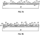
- Fig. 7A through Fig. 7F depict an alternative process for electrophoretically depositing a phosphor layer on a LED chip 10 that includes a nonconductive substrate.
- Fig. 7A, Fig. 7B , and Fig. 7C depict the stages depicted in Fig. 4A, Fig. 4B, and Fig. 4C , respectively.
- submount 28 is coated with first insulating layer 60
- contact layer 62 is deposited on top of first insulating layer 60 to form anode and cathode contacts
- metal bumps 52 are formed on contact layer 62.
- second insulating layer 66 is deposited on contact layer 62, leaving contact windows 68 exposed.
- LED chip 10 is placed on and attached to metal bumps 52.
- Fig. 7D depicts a stage whereby all surfaces are coated with electroconductive layer 88.
- electroconductive layer 88 in Fig. 7D coats both LED chip 10 and second insulating layer 66, making all surfaces conductive.
- Fig. 7E depicts a selective insulation of electroconductive-layer-coated surfaces where phosphor deposition is not desired.
- Surfaces where phosphor deposition is not desired may be selectively coated with insulating photoresist 70, for example using a patterned mask. By using the patterned mask, only the surfaces of LED chip 10 may remain conductive, uncoated with photoresist 70.
- Gap 46 surrounds the side walls of LED chip 10, separating the side walls from photoresist 70 and allowing phosphor deposition on the side walls of LED chip 10. Gap 46 is wide enough to allow phosphor particles to reach the side walls of LED chip 10, but usually less than 100 ⁇ m wide.
- Fig. 7F depicts immersion of all surfaces in solution 84 containing phosphor particles. Different biases are applied to submount 28 and electrode 82, and the difference in biases push phosphor particles out of solution 84 onto electroconductive layer 88, as shown by arrows 86. Gap 46 allows phosphor articles to deposit on the side walls of LED chip 10, conformally coating LED chip 10.
- a transparent binder material may be used to secure the adhesion of phosphor particles onto a surface.
- the binder material is selected to have a refractive index of at least 1.4.
- the transparent binder material may be co-deposited from the electrophoretic solution along with the phosphor powder, or infused into the phosphor matrix by selective deposition and capillary action after the phosphor powder is deposited.
- the binder material may be an organic material such as an optical coupling epoxy (e.g., PT 1002 from Pacific Polymer Technology), an optical coupling silicone (e.g., silicone supplied by Nye Lubricants), inorganic metal oxide or glass frit powder (e.g., a PbO-based glass), or sol-gel. Further details on the binder material is provided in U.S. Patent No. 6,180,029 to Mark J. Hampden-Smith, et al titled "Oxygen-containing Phosphor Powders, Methods for Making Phosphor Powders and Devices Incorporating the Same," which is herein incorporated by reference.
- U.S. Patent Application Serial No. XXX (Attorney Docket No. M-11473 US) discusses using sol-gel as a binder material, and is herein incorporated by reference.
- Fig. 8A shows a light emitting device including LED chip 10 and a conformal phosphor layer 12. Absence of electroconductive layer 88 indicates that the particular LED chip 10 includes a conductive substrate, and that phosphor layer 12 was created by the process depicted in Fig. 4A through Fig. 4E .
- Phosphor layer 12 has a substantially uniform thickness above the top surface and is adjacent to all surfaces of LED chip 10 except the surface that is attached to submount 28. In one embodiment, any variations in the thickness of phosphor layer 12 are less than 10% of the thickness of phosphor layer 12, and typically less than 5% of the thickness of phosphor layer 12. Thus, every light path out of phosphor layer 12 has substantially the same length, reducing nonuniformity in the color of light emitted from the source.
- the thickness of phosphor layer 12 is about 15 ⁇ m to about 100 ⁇ m.
- Fig. 8B depicts a light emitting device created either by the process depicted in Fig. 6A through 6E or by the process depicted in Fig. 7A through 7F .
- the light emitting device depicted in Fig. 8B includes electroconductive layer 88 in addition to LED chip 10 with a nonconductive substrate and phosphor layer 12, unlike the light emitting device in Fig. 8A . If a binder material is infused into the phosphor layer after the phosphor powder is deposited, there may be an extra binder layer coating phosphor layer 12.
- Phosphor layer 12 is close enough to LED chip 10 that it does not significantly increase the size of the light emitting device over the size of LED chip 10.
- phosphor layer 12 is adjacent to LED chip 10.
- the thickness of phosphor layer 12 is less than 10% of a cross sectional dimension of the LED, e.g., the length of the LED.
- a typical cross sectional dimension of LED chip 10 is 1 mm.
- a phosphor-coated LED according to embodiments of the present invention does not require optics substantially larger than optics required to control the light out of an LED that is not phosphor coated.
- phosphor layer 12 may include a closely-packed particle layer in order to achieve a thin layer. Multiple phosphors or particles such as titanium dioxide or silicon dioxide may be used to modify the density of phosphor layer 12.
- phosphor layer 12 In order to maintain a substantial uniformity of the path length through the phosphor, and therefore of the color of light emitted from the source, phosphor layer 12 should be the only phosphor path through which light from the LED passes. Any phosphor coatings on submount 28, or on any optics such as reflector cups or reflecting planes which may extend the phosphor layer by more than either 10% of the cross-sectional dimension of LED chip 10 or by 100 ⁇ m beyond the boundaries of the LED chip, are avoided.
- the exit path length for light through the phosphor layer does not vary by more than 10%, due to the uniform layer thickness.
- the volume of the light emitting device is larger than the volume of LED chip 10 by only the thickness of the phosphor layer necessary to create the output spectrum. This layer thickness is typically less than 30-microns thick.
- masking errors do not perturb, to a first order, nor define the emissive phosphor pattern of the source. Thus, very little precision is required for the masking process.
Landscapes
- Chemical & Material Sciences (AREA)
- Inorganic Chemistry (AREA)
- Engineering & Computer Science (AREA)
- Chemical Kinetics & Catalysis (AREA)
- Electrochemistry (AREA)
- Materials Engineering (AREA)
- Metallurgy (AREA)
- Organic Chemistry (AREA)
- Led Device Packages (AREA)
- Luminescent Compositions (AREA)
- Led Devices (AREA)
Claims (11)
- Verfahren zum konformen Beschichten einer Licht emittierenden Halbleiterstruktur (10) mit Phosphor, wobei das Verfahren umfasst:Bereitstellen einer Montagebasis (28) mit einer leitenden Region (62);elektrisches Koppeln einer Licht emittierenden Halbleiterstruktur mit der leitenden Region;Anlegen einer ersten Vorspannung an geladene Phosphorteilchen in einer Lösung; undAnlegen einer zweiten Vorspannung an die leitende Region, um zu veranlassen, dass die Phosphorteilchen im Wesentlichen konform auf mindestens eine Oberfläche der Licht emittierenden Halbleiterstruktur abgeschieden werden.
- Verfahren nach Anspruch 1, wobei die Licht emittierende Halbleiterstruktur ein leitendes Substrat umfasst.
- Verfahren nach Anspruch 1, ferner umfassend ein Eintauchen der leitenden Region und der Licht emittierenden Halbleiterstruktur in die Lösung.
- Verfahren nach Anspruch 1, wobei die Phosphorteilchen eine Strontium-Sulfid-Verbindung, eine Yttrium-Aluminium-Granat-Verbindung, die mit mindestens einem von Gadolinium, Cer und Praseodym dotiert ist, eine Strontium-Thiogallat-Verbindung oder ein Polymer mit einem organischen lumineszierenden Farbstoff umfassen.
- Verfahren nach Anspruch 1, wobei die Lösung ein transparentes Bindermaterial zum Sichern der Haftung der Phosphorteilchen an der leitenden Region umfasst, wobei das transparente Bindermaterial einen Brechungsindex von mindestens 1,4 aufweist.
- Verfahren nach Anspruch 1, wobei die Lösung ein Aufladungsmittel zum Aufladen der Phosphorteilchen umfasst.
- Verfahren nach Anspruch 1, ferner umfassend ein Infundieren eines transparenten Bindermaterials in eine Matrix der auf die leitende Region abgeschiedenen Phosphorteilchen, wobei das Bindermaterial die Haftung der Phosphorteilchen auf der leitenden Region fördert und einen Brechungsindex von mindestens 1,4 aufweist.
- Verfahren nach Anspruch 1, ferner umfassend:Abscheiden einer Schicht elektrisch leitenden Materials auf Oberflächen der Licht emittierenden Halbleiterstruktur und auf Oberflächen der Montagebasis; undVerhindern von Phosphorabscheidung auf einen Teil der Schicht elektrisch leitenden Materials durch Beschichten mit einem nichtleitenden Material.
- Verfahren nach Anspruch 8, wobei das Abscheiden ein Befeuchten der Oberfläche der Licht emittierenden Halbleiterstruktur mit einer Lösung umfasst, die Antimonzinnoxid umfasst.
- Verfahren zum konformen Beschichten einer Licht emittierenden Halbleiterstruktur (10) mit Phosphor, wobei das Verfahren umfasst:Bereitstellen einer Licht emittieren Halbleiterstruktur mit einer Anode (20b) und einer Kathode (20a), die an eine erste Vorspannung angeschlossen sind;Anlegen einer zweiten Vorspannung an eine Lösung geladenen Phosphors; undEintauchen der Licht emittierenden Halbleiterstruktur in die Lösung, um die Licht emittierende Halbleiterstruktur im Wesentlichen konform mit den Phosphorteilchen zu beschichten.
- Verfahren nach Anspruch 10, ferner umfassend ein Bilden einer Schicht leitenden Materials über mindestens einer Oberfläche der Licht emittierenden Halbleiterstruktur, die mit dem Phosphor beschichtet werden soll.
Applications Claiming Priority (2)
| Application Number | Priority Date | Filing Date | Title |
|---|---|---|---|
| US09/879,627 US6576488B2 (en) | 2001-06-11 | 2001-06-11 | Using electrophoresis to produce a conformally coated phosphor-converted light emitting semiconductor |
| US879627 | 2001-06-11 |
Publications (3)
| Publication Number | Publication Date |
|---|---|
| EP1267424A2 EP1267424A2 (de) | 2002-12-18 |
| EP1267424A3 EP1267424A3 (de) | 2010-10-06 |
| EP1267424B1 true EP1267424B1 (de) | 2018-03-14 |
Family
ID=25374532
Family Applications (1)
| Application Number | Title | Priority Date | Filing Date |
|---|---|---|---|
| EP02077252.1A Expired - Lifetime EP1267424B1 (de) | 2001-06-11 | 2002-06-10 | Verfahren zum angepassten Beschichten einer Leuchtdiode mit einem Phosphor mittels Elektrophorese |
Country Status (4)
| Country | Link |
|---|---|
| US (1) | US6576488B2 (de) |
| EP (1) | EP1267424B1 (de) |
| JP (1) | JP4336480B2 (de) |
| TW (1) | TW544954B (de) |
Families Citing this family (234)
| Publication number | Priority date | Publication date | Assignee | Title |
|---|---|---|---|---|
| US6600175B1 (en) * | 1996-03-26 | 2003-07-29 | Advanced Technology Materials, Inc. | Solid state white light emitter and display using same |
| US6650044B1 (en) * | 2000-10-13 | 2003-11-18 | Lumileds Lighting U.S., Llc | Stenciling phosphor layers on light emitting diodes |
| US6878973B2 (en) * | 2001-08-23 | 2005-04-12 | Lumileds Lighting U.S., Llc | Reduction of contamination of light emitting devices |
| US7224856B2 (en) * | 2001-10-23 | 2007-05-29 | Digital Optics Corporation | Wafer based optical chassis and associated methods |
| US6841802B2 (en) | 2002-06-26 | 2005-01-11 | Oriol, Inc. | Thin film light emitting diode |
| US7423296B2 (en) * | 2003-02-26 | 2008-09-09 | Avago Technologies Ecbu Ip Pte Ltd | Apparatus for producing a spectrally-shifted light output from a light emitting device utilizing thin-film luminescent layers |
| US7005679B2 (en) * | 2003-05-01 | 2006-02-28 | Cree, Inc. | Multiple component solid state white light |
| US7633093B2 (en) * | 2003-05-05 | 2009-12-15 | Lighting Science Group Corporation | Method of making optical light engines with elevated LEDs and resulting product |
| US7528421B2 (en) * | 2003-05-05 | 2009-05-05 | Lamina Lighting, Inc. | Surface mountable light emitting diode assemblies packaged for high temperature operation |
| US7777235B2 (en) | 2003-05-05 | 2010-08-17 | Lighting Science Group Corporation | Light emitting diodes with improved light collimation |
| US7157745B2 (en) * | 2004-04-09 | 2007-01-02 | Blonder Greg E | Illumination devices comprising white light emitting diodes and diode arrays and method and apparatus for making them |
| US8075147B2 (en) * | 2003-05-13 | 2011-12-13 | Light Prescriptions Innovators, Llc | Optical device for LED-based lamp |
| US6803607B1 (en) * | 2003-06-13 | 2004-10-12 | Cotco Holdings Limited | Surface mountable light emitting device |
| US7075225B2 (en) * | 2003-06-27 | 2006-07-11 | Tajul Arosh Baroky | White light emitting device |
| US7462983B2 (en) * | 2003-06-27 | 2008-12-09 | Avago Technologies Ecbu Ip (Singapore) Pte. Ltd. | White light emitting device |
| US7915085B2 (en) | 2003-09-18 | 2011-03-29 | Cree, Inc. | Molded chip fabrication method |
| KR100550548B1 (ko) * | 2003-09-30 | 2006-02-10 | 엘지전자 주식회사 | 평판 디스플레이 패널의 형광막 형성장치 |
| KR20050034936A (ko) * | 2003-10-10 | 2005-04-15 | 삼성전기주식회사 | 형광체를 이용한 파장변환형 발광 다이오드 패키지 및제조방법 |
| DE202005002110U1 (de) * | 2004-02-19 | 2005-05-04 | Hong-Yuan Technology Co., Ltd., Yonghe | Lichtemittierende Vorrichtung |
| EP1721340A1 (de) * | 2004-02-23 | 2006-11-15 | Hong-Yuan Technology Co., Ltd. | Lichtemissionsbauelement und herstellungsverfahren dafür |
| CN100392879C (zh) * | 2004-02-23 | 2008-06-04 | 弘元科技有限公司 | 发光装置及其制造方法和制造系统 |
| EP1566426B1 (de) | 2004-02-23 | 2015-12-02 | Philips Lumileds Lighting Company LLC | Lichtemittierende vorrichtung, enthaltend einen wellenlängenkonvertierenden leuchtstoff |
| US7250715B2 (en) | 2004-02-23 | 2007-07-31 | Philips Lumileds Lighting Company, Llc | Wavelength converted semiconductor light emitting devices |
| US6924233B1 (en) * | 2004-03-19 | 2005-08-02 | Agilent Technologies, Inc. | Phosphor deposition methods |
| US7517728B2 (en) | 2004-03-31 | 2009-04-14 | Cree, Inc. | Semiconductor light emitting devices including a luminescent conversion element |
| US20070267646A1 (en) * | 2004-06-03 | 2007-11-22 | Philips Lumileds Lighting Company, Llc | Light Emitting Device Including a Photonic Crystal and a Luminescent Ceramic |
| US7361938B2 (en) | 2004-06-03 | 2008-04-22 | Philips Lumileds Lighting Company Llc | Luminescent ceramic for a light emitting device |
| US7553683B2 (en) * | 2004-06-09 | 2009-06-30 | Philips Lumiled Lighting Co., Llc | Method of forming pre-fabricated wavelength converting elements for semiconductor light emitting devices |
| US20060006793A1 (en) * | 2004-07-12 | 2006-01-12 | Baroky Tajul A | Deep ultraviolet used to produce white light |
| KR100707100B1 (ko) * | 2004-10-01 | 2007-04-13 | 엘지이노텍 주식회사 | 발광 다이오드 및 그 제조방법 |
| US7462502B2 (en) * | 2004-11-12 | 2008-12-09 | Philips Lumileds Lighting Company, Llc | Color control by alteration of wavelength converting element |
| US7419839B2 (en) * | 2004-11-12 | 2008-09-02 | Philips Lumileds Lighting Company, Llc | Bonding an optical element to a light emitting device |
| US7452737B2 (en) * | 2004-11-15 | 2008-11-18 | Philips Lumileds Lighting Company, Llc | Molded lens over LED die |
| US7352011B2 (en) | 2004-11-15 | 2008-04-01 | Philips Lumileds Lighting Company, Llc | Wide emitting lens for LED useful for backlighting |
| US7858408B2 (en) * | 2004-11-15 | 2010-12-28 | Koninklijke Philips Electronics N.V. | LED with phosphor tile and overmolded phosphor in lens |
| US7344902B2 (en) | 2004-11-15 | 2008-03-18 | Philips Lumileds Lighting Company, Llc | Overmolded lens over LED die |
| KR101106148B1 (ko) * | 2004-12-14 | 2012-01-20 | 서울옵토디바이스주식회사 | 발광 소자 |
| WO2006098545A2 (en) | 2004-12-14 | 2006-09-21 | Seoul Opto Device Co., Ltd. | Light emitting device having a plurality of light emitting cells and package mounting the same |
| JP4687109B2 (ja) * | 2005-01-07 | 2011-05-25 | ソニー株式会社 | 集積型発光ダイオードの製造方法 |
| US8680534B2 (en) * | 2005-01-11 | 2014-03-25 | Semileds Corporation | Vertical light emitting diodes (LED) having metal substrate and spin coated phosphor layer for producing white light |
| US7646033B2 (en) * | 2005-01-11 | 2010-01-12 | Semileds Corporation | Systems and methods for producing white-light light emitting diodes |
| US7195944B2 (en) * | 2005-01-11 | 2007-03-27 | Semileds Corporation | Systems and methods for producing white-light emitting diodes |
| US8012774B2 (en) * | 2005-01-11 | 2011-09-06 | SemiLEDs Optoelectronics Co., Ltd. | Coating process for a light-emitting diode (LED) |
| JP4792751B2 (ja) * | 2005-01-26 | 2011-10-12 | 日亜化学工業株式会社 | 発光装置およびその製造方法 |
| CN101138278A (zh) * | 2005-03-09 | 2008-03-05 | 皇家飞利浦电子股份有限公司 | 包括辐射源和荧光材料的照明系统 |
| US8076680B2 (en) * | 2005-03-11 | 2011-12-13 | Seoul Semiconductor Co., Ltd. | LED package having an array of light emitting cells coupled in series |
| KR101241973B1 (ko) * | 2005-03-11 | 2013-03-08 | 서울반도체 주식회사 | 발광 장치 및 이의 제조 방법 |
| US8748923B2 (en) * | 2005-03-14 | 2014-06-10 | Philips Lumileds Lighting Company Llc | Wavelength-converted semiconductor light emitting device |
| US7341878B2 (en) * | 2005-03-14 | 2008-03-11 | Philips Lumileds Lighting Company, Llc | Wavelength-converted semiconductor light emitting device |
| US7535524B2 (en) * | 2005-04-18 | 2009-05-19 | Avago Technologies Ecbu Ip (Singapore) Pte. Ltd. | Display panel with wavelength converting material and control interface to switchably control independent projection or non-projection of primary and secondary IMAGES |
| US7736945B2 (en) * | 2005-06-09 | 2010-06-15 | Philips Lumileds Lighting Company, Llc | LED assembly having maximum metal support for laser lift-off of growth substrate |
| JP2008545269A (ja) * | 2005-07-01 | 2008-12-11 | ラミナ ライティング インコーポレーテッド | 白色発光ダイオード及びダイオードアレイを有する照明装置、それらの製造方法及び製造装置 |
| US8563339B2 (en) | 2005-08-25 | 2013-10-22 | Cree, Inc. | System for and method for closed loop electrophoretic deposition of phosphor materials on semiconductor devices |
| US7847302B2 (en) * | 2005-08-26 | 2010-12-07 | Koninklijke Philips Electronics, N.V. | Blue LED with phosphor layer for producing white light and different phosphor in outer lens for reducing color temperature |
| US20070076412A1 (en) * | 2005-09-30 | 2007-04-05 | Lumileds Lighting U.S., Llc | Light source with light emitting array and collection optic |
| US7543959B2 (en) * | 2005-10-11 | 2009-06-09 | Philips Lumiled Lighting Company, Llc | Illumination system with optical concentrator and wavelength converting element |
| JP4810977B2 (ja) * | 2005-11-08 | 2011-11-09 | 日亜化学工業株式会社 | 発光装置およびその形成方法 |
| US7514721B2 (en) * | 2005-11-29 | 2009-04-07 | Koninklijke Philips Electronics N.V. | Luminescent ceramic element for a light emitting device |
| TWI396814B (zh) | 2005-12-22 | 2013-05-21 | 克里公司 | 照明裝置 |
| EP1974389A4 (de) | 2006-01-05 | 2010-12-29 | Illumitex Inc | Separate optische vorrichtung zur lichtorientierung von einer led |
| KR100723247B1 (ko) * | 2006-01-10 | 2007-05-29 | 삼성전기주식회사 | 칩코팅형 led 패키지 및 그 제조방법 |
| WO2007080555A1 (en) | 2006-01-16 | 2007-07-19 | Koninklijke Philips Electronics N.V. | Phosphor converted light emitting device |
| JP2009524212A (ja) * | 2006-01-16 | 2009-06-25 | コーニンクレッカ フィリップス エレクトロニクス エヌ ヴィ | Eu含有蛍光体材料を有する発光装置 |
| US20090008655A1 (en) * | 2006-01-31 | 2009-01-08 | Koninklijke Philips Electronics N.V. | White Light Source |
| US8124957B2 (en) | 2006-02-22 | 2012-02-28 | Cree, Inc. | Low resistance tunnel junctions in wide band gap materials and method of making same |
| US7737451B2 (en) * | 2006-02-23 | 2010-06-15 | Cree, Inc. | High efficiency LED with tunnel junction layer |
| US9335006B2 (en) * | 2006-04-18 | 2016-05-10 | Cree, Inc. | Saturated yellow phosphor converted LED and blue converted red LED |
| JP5308618B2 (ja) * | 2006-04-26 | 2013-10-09 | 日亜化学工業株式会社 | 半導体発光装置 |
| CN100472828C (zh) * | 2006-04-28 | 2009-03-25 | 佰鸿工业股份有限公司 | 白光发光二极管的制作方法 |
| JP4961827B2 (ja) * | 2006-05-11 | 2012-06-27 | 日亜化学工業株式会社 | 発光装置及びその製造方法 |
| US8062925B2 (en) * | 2006-05-16 | 2011-11-22 | Koninklijke Philips Electronics N.V. | Process for preparing a semiconductor light-emitting device for mounting |
| US7655486B2 (en) * | 2006-05-17 | 2010-02-02 | 3M Innovative Properties Company | Method of making light emitting device with multilayer silicon-containing encapsulant |
| US8947619B2 (en) | 2006-07-06 | 2015-02-03 | Intematix Corporation | Photoluminescence color display comprising quantum dots material and a wavelength selective filter that allows passage of excitation radiation and prevents passage of light generated by photoluminescence materials |
| US20080074583A1 (en) * | 2006-07-06 | 2008-03-27 | Intematix Corporation | Photo-luminescence color liquid crystal display |
| US20080029720A1 (en) * | 2006-08-03 | 2008-02-07 | Intematix Corporation | LED lighting arrangement including light emitting phosphor |
| US8092735B2 (en) * | 2006-08-17 | 2012-01-10 | 3M Innovative Properties Company | Method of making a light emitting device having a molded encapsulant |
| DE102006047045A1 (de) * | 2006-10-02 | 2008-04-03 | Universität Paderborn | Photovoltaische Einrichtung |
| US7789531B2 (en) | 2006-10-02 | 2010-09-07 | Illumitex, Inc. | LED system and method |
| US20080151143A1 (en) * | 2006-10-19 | 2008-06-26 | Intematix Corporation | Light emitting diode based backlighting for color liquid crystal displays |
| US7504272B2 (en) * | 2006-11-06 | 2009-03-17 | Stanley Electric Co., Ltd. | Method for producing color-converting light-emitting device using electrophoresis |
| US7521862B2 (en) * | 2006-11-20 | 2009-04-21 | Philips Lumileds Lighting Co., Llc | Light emitting device including luminescent ceramic and light-scattering material |
| TW201448263A (zh) | 2006-12-11 | 2014-12-16 | 美國加利福尼亞大學董事會 | 透明發光二極體 |
| US8704254B2 (en) | 2006-12-22 | 2014-04-22 | Philips Lumileds Lighting Company, Llc | Light emitting device including a filter |
| US7902564B2 (en) * | 2006-12-22 | 2011-03-08 | Koninklijke Philips Electronics N.V. | Multi-grain luminescent ceramics for light emitting devices |
| US20080192458A1 (en) | 2007-02-12 | 2008-08-14 | Intematix Corporation | Light emitting diode lighting system |
| US7972030B2 (en) * | 2007-03-05 | 2011-07-05 | Intematix Corporation | Light emitting diode (LED) based lighting systems |
| US8203260B2 (en) * | 2007-04-13 | 2012-06-19 | Intematix Corporation | Color temperature tunable white light source |
| TWI350012B (en) * | 2007-05-04 | 2011-10-01 | Lite On Technology Corp | White light emitting diode and base thereof |
| US7703943B2 (en) * | 2007-05-07 | 2010-04-27 | Intematix Corporation | Color tunable light source |
| JP5006102B2 (ja) | 2007-05-18 | 2012-08-22 | 株式会社東芝 | 発光装置およびその製造方法 |
| TWI347687B (en) * | 2007-07-13 | 2011-08-21 | Lite On Technology Corp | Light-emitting device with open-loop control |
| JP5043554B2 (ja) * | 2007-08-07 | 2012-10-10 | スタンレー電気株式会社 | 半導体発光装置 |
| US7810956B2 (en) * | 2007-08-23 | 2010-10-12 | Koninklijke Philips Electronics N.V. | Light source including reflective wavelength-converting layer |
| US11114594B2 (en) | 2007-08-24 | 2021-09-07 | Creeled, Inc. | Light emitting device packages using light scattering particles of different size |
| DE102007042642A1 (de) * | 2007-09-07 | 2009-03-12 | Osram Gesellschaft mit beschränkter Haftung | Verfahren zum Herstellen eines optoelektronischen Bauelements und optoelektronisches Bauelement |
| US20090065792A1 (en) | 2007-09-07 | 2009-03-12 | 3M Innovative Properties Company | Method of making an led device having a dome lens |
| US8783887B2 (en) | 2007-10-01 | 2014-07-22 | Intematix Corporation | Color tunable light emitting device |
| US7915627B2 (en) | 2007-10-17 | 2011-03-29 | Intematix Corporation | Light emitting device with phosphor wavelength conversion |
| TWI401820B (zh) * | 2007-11-07 | 2013-07-11 | 財團法人工業技術研究院 | 發光元件及其製作方法 |
| US8946987B2 (en) | 2007-11-07 | 2015-02-03 | Industrial Technology Research Institute | Light emitting device and fabricating method thereof |
| US8940561B2 (en) * | 2008-01-15 | 2015-01-27 | Cree, Inc. | Systems and methods for application of optical materials to optical elements |
| US8058088B2 (en) | 2008-01-15 | 2011-11-15 | Cree, Inc. | Phosphor coating systems and methods for light emitting structures and packaged light emitting diodes including phosphor coating |
| EP2240968A1 (de) | 2008-02-08 | 2010-10-20 | Illumitex, Inc. | System und verfahren zur bildung einer emitterschicht |
| CN102016402A (zh) * | 2008-02-21 | 2011-04-13 | 光处方革新有限公司 | 球形发射远距离磷光体 |
| US8740400B2 (en) | 2008-03-07 | 2014-06-03 | Intematix Corporation | White light illumination system with narrow band green phosphor and multiple-wavelength excitation |
| US8567973B2 (en) * | 2008-03-07 | 2013-10-29 | Intematix Corporation | Multiple-chip excitation systems for white light emitting diodes (LEDs) |
| US8637883B2 (en) | 2008-03-19 | 2014-01-28 | Cree, Inc. | Low index spacer layer in LED devices |
| KR100973238B1 (ko) * | 2008-03-26 | 2010-07-30 | 서울반도체 주식회사 | 형광체 코팅방법 및 장치 그리고 형광체 코팅층을 포함하는led |
| TW200941761A (en) * | 2008-03-27 | 2009-10-01 | Liung Feng Ind Co Ltd | Packaging process of a light emitting component |
| US9287469B2 (en) * | 2008-05-02 | 2016-03-15 | Cree, Inc. | Encapsulation for phosphor-converted white light emitting diode |
| JP2011523511A (ja) | 2008-05-29 | 2011-08-11 | クリー インコーポレイテッド | 近距離場で光を混合する光源 |
| US7928458B2 (en) * | 2008-07-15 | 2011-04-19 | Visera Technologies Company Limited | Light-emitting diode device and method for fabricating the same |
| US20100027293A1 (en) * | 2008-07-30 | 2010-02-04 | Intematix Corporation | Light Emitting Panel |
| US8822954B2 (en) * | 2008-10-23 | 2014-09-02 | Intematix Corporation | Phosphor based authentication system |
| US20100123386A1 (en) * | 2008-11-13 | 2010-05-20 | Maven Optronics Corp. | Phosphor-Coated Light Extraction Structures for Phosphor-Converted Light Emitting Devices |
| JP4868427B2 (ja) * | 2008-11-13 | 2012-02-01 | 国立大学法人名古屋大学 | 半導体発光装置 |
| KR101154758B1 (ko) * | 2008-11-18 | 2012-06-08 | 엘지이노텍 주식회사 | 반도체 발광소자 및 이를 구비한 발광소자 패키지 |
| TW201034256A (en) | 2008-12-11 | 2010-09-16 | Illumitex Inc | Systems and methods for packaging light-emitting diode devices |
| US8169135B2 (en) * | 2008-12-17 | 2012-05-01 | Lednovation, Inc. | Semiconductor lighting device with wavelength conversion on back-transferred light path |
| US8390193B2 (en) * | 2008-12-31 | 2013-03-05 | Intematix Corporation | Light emitting device with phosphor wavelength conversion |
| US7811918B1 (en) | 2009-01-09 | 2010-10-12 | The United States Of America As Represented By The Secretary Of The Navy | Electric current induced liquid metal flow and metallic conformal coating of conductive templates |
| US20100187961A1 (en) * | 2009-01-27 | 2010-07-29 | Keith Scott | Phosphor housing for light emitting diode lamp |
| CN101499446B (zh) * | 2009-02-26 | 2013-10-16 | 光宝电子(广州)有限公司 | 导线架料片、封装结构以及发光二极管封装结构 |
| US7994531B2 (en) | 2009-04-02 | 2011-08-09 | Visera Technologies Company Limited | White-light light emitting diode chips and fabrication methods thereof |
| CN101551068A (zh) * | 2009-04-30 | 2009-10-07 | 旭丽电子(广州)有限公司 | 一种发光二极管装置及其封装方法 |
| JP2010267646A (ja) * | 2009-05-12 | 2010-11-25 | Nichia Corp | 発光装置 |
| US8247248B2 (en) * | 2009-05-15 | 2012-08-21 | Achrolux Inc. | Methods and apparatus for forming uniform layers of phosphor material on an LED encapsulation structure |
| US8651692B2 (en) * | 2009-06-18 | 2014-02-18 | Intematix Corporation | LED based lamp and light emitting signage |
| US20100327300A1 (en) * | 2009-06-25 | 2010-12-30 | Koninklijke Philips Electronics N.V. | Contact for a semiconductor light emitting device |
| WO2010151600A1 (en) | 2009-06-27 | 2010-12-29 | Michael Tischler | High efficiency leds and led lamps |
| US8449128B2 (en) | 2009-08-20 | 2013-05-28 | Illumitex, Inc. | System and method for a lens and phosphor layer |
| US8585253B2 (en) | 2009-08-20 | 2013-11-19 | Illumitex, Inc. | System and method for color mixing lens array |
| US8455910B2 (en) * | 2009-09-21 | 2013-06-04 | Walsin Lihwa Corporation | Method of manufacturing light emitting diode packaging lens and light emitting diode package |
| WO2011037877A1 (en) | 2009-09-25 | 2011-03-31 | Cree, Inc. | Lighting device with low glare and high light level uniformity |
| US20110110095A1 (en) * | 2009-10-09 | 2011-05-12 | Intematix Corporation | Solid-state lamps with passive cooling |
| TWI403005B (zh) | 2009-10-12 | 2013-07-21 | 英特明光能股份有限公司 | 發光二極體及其製作方法 |
| US8779685B2 (en) * | 2009-11-19 | 2014-07-15 | Intematix Corporation | High CRI white light emitting devices and drive circuitry |
| US8466611B2 (en) | 2009-12-14 | 2013-06-18 | Cree, Inc. | Lighting device with shaped remote phosphor |
| JP4991834B2 (ja) | 2009-12-17 | 2012-08-01 | シャープ株式会社 | 車両用前照灯 |
| US20110149548A1 (en) * | 2009-12-22 | 2011-06-23 | Intematix Corporation | Light emitting diode based linear lamps |
| GB2488936B (en) * | 2009-12-26 | 2015-03-25 | Achrolux Inc | Uniform film-layered structure that converts the wavelengh of emitted light and method for forming the same |
| US8653539B2 (en) | 2010-01-04 | 2014-02-18 | Cooledge Lighting, Inc. | Failure mitigation in arrays of light-emitting devices |
| US9480133B2 (en) | 2010-01-04 | 2016-10-25 | Cooledge Lighting Inc. | Light-emitting element repair in array-based lighting devices |
| JP5232815B2 (ja) | 2010-02-10 | 2013-07-10 | シャープ株式会社 | 車両用前照灯 |
| KR100969100B1 (ko) * | 2010-02-12 | 2010-07-09 | 엘지이노텍 주식회사 | 발광소자, 발광소자의 제조방법 및 발광소자 패키지 |
| JP5614675B2 (ja) * | 2010-02-16 | 2014-10-29 | 独立行政法人物質・材料研究機構 | 波長変換部材の製造方法 |
| EP2541631A4 (de) | 2010-02-25 | 2015-03-18 | Lightizer Korea Co Ltd | Lichtemittierende diode und verfahren zu ihrer herstellung |
| US8273589B2 (en) * | 2010-03-19 | 2012-09-25 | Micron Technology, Inc. | Light emitting diodes and methods for manufacturing light emitting diodes |
| TWI456798B (zh) * | 2010-04-23 | 2014-10-11 | 璨圓光電股份有限公司 | 發光裝置之製造方法 |
| JP5112476B2 (ja) * | 2010-06-28 | 2013-01-09 | シャープ株式会社 | 発光体、発光装置、照明装置および車両用前照灯 |
| US8733996B2 (en) | 2010-05-17 | 2014-05-27 | Sharp Kabushiki Kaisha | Light emitting device, illuminating device, and vehicle headlamp |
| US8807799B2 (en) | 2010-06-11 | 2014-08-19 | Intematix Corporation | LED-based lamps |
| US8888318B2 (en) | 2010-06-11 | 2014-11-18 | Intematix Corporation | LED spotlight |
| CN102959708B (zh) | 2010-06-29 | 2016-05-04 | 柯立芝照明有限公司 | 具有易弯曲基板的电子装置 |
| US8946998B2 (en) | 2010-08-09 | 2015-02-03 | Intematix Corporation | LED-based light emitting systems and devices with color compensation |
| US9070851B2 (en) | 2010-09-24 | 2015-06-30 | Seoul Semiconductor Co., Ltd. | Wafer-level light emitting diode package and method of fabricating the same |
| US9546765B2 (en) | 2010-10-05 | 2017-01-17 | Intematix Corporation | Diffuser component having scattering particles |
| US8614539B2 (en) | 2010-10-05 | 2013-12-24 | Intematix Corporation | Wavelength conversion component with scattering particles |
| US8957585B2 (en) | 2010-10-05 | 2015-02-17 | Intermatix Corporation | Solid-state light emitting devices with photoluminescence wavelength conversion |
| US8604678B2 (en) | 2010-10-05 | 2013-12-10 | Intematix Corporation | Wavelength conversion component with a diffusing layer |
| US8610341B2 (en) | 2010-10-05 | 2013-12-17 | Intematix Corporation | Wavelength conversion component |
| WO2012047937A1 (en) | 2010-10-05 | 2012-04-12 | Intematix Corporation | Solid-state light emitting devices and signage with photoluminescence wavelength conversion |
| CN104091815A (zh) * | 2010-10-12 | 2014-10-08 | 晶元光电股份有限公司 | 发光元件 |
| KR101856801B1 (ko) * | 2010-10-12 | 2018-05-10 | 루미리즈 홀딩 비.브이. | 발광 장치 및 그 제조 방법 |
| TWI447969B (zh) | 2010-10-20 | 2014-08-01 | 英特明光能股份有限公司 | 發光二極體封裝結構 |
| JP5472031B2 (ja) * | 2010-10-21 | 2014-04-16 | 日亜化学工業株式会社 | 発光装置及びその製造方法 |
| CN102451812B (zh) * | 2010-10-26 | 2014-02-19 | 展晶科技(深圳)有限公司 | 荧光粉涂布方法 |
| US9816677B2 (en) | 2010-10-29 | 2017-11-14 | Sharp Kabushiki Kaisha | Light emitting device, vehicle headlamp, illumination device, and laser element |
| US9478719B2 (en) | 2010-11-08 | 2016-10-25 | Bridgelux, Inc. | LED-based light source utilizing asymmetric conductors |
| US8455895B2 (en) * | 2010-11-08 | 2013-06-04 | Bridgelux, Inc. | LED-based light source utilizing asymmetric conductors |
| US8354684B2 (en) | 2011-01-09 | 2013-01-15 | Bridgelux, Inc. | Packaging photon building blocks having only top side connections in an interconnect structure |
| US8652860B2 (en) | 2011-01-09 | 2014-02-18 | Bridgelux, Inc. | Packaging photon building blocks having only top side connections in a molded interconnect structure |
| US9166126B2 (en) * | 2011-01-31 | 2015-10-20 | Cree, Inc. | Conformally coated light emitting devices and methods for providing the same |
| US9508904B2 (en) | 2011-01-31 | 2016-11-29 | Cree, Inc. | Structures and substrates for mounting optical elements and methods and devices for providing the same background |
| US20120205695A1 (en) * | 2011-02-16 | 2012-08-16 | Tzu-Han Lin | Light-emitting diode device |
| JP5962102B2 (ja) * | 2011-03-24 | 2016-08-03 | 日亜化学工業株式会社 | 発光装置及びその製造方法 |
| US9004705B2 (en) | 2011-04-13 | 2015-04-14 | Intematix Corporation | LED-based light sources for light emitting devices and lighting arrangements with photoluminescence wavelength conversion |
| US9029887B2 (en) | 2011-04-22 | 2015-05-12 | Micron Technology, Inc. | Solid state lighting devices having improved color uniformity and associated methods |
| US9263636B2 (en) * | 2011-05-04 | 2016-02-16 | Cree, Inc. | Light-emitting diode (LED) for achieving an asymmetric light output |
| EP2718970A2 (de) * | 2011-06-10 | 2014-04-16 | Koninklijke Philips N.V. | Led-anordnung mit teilchenstreuung auf den leds und herstellungsverfahren dafür |
| KR101171331B1 (ko) * | 2011-06-16 | 2012-08-10 | 서울옵토디바이스주식회사 | 발광 소자 |
| TWI523278B (zh) | 2011-08-05 | 2016-02-21 | 晶元光電股份有限公司 | 波長轉換結構及其製造方法以及包含此波長轉換結構之發光裝置 |
| DE102011111980A1 (de) * | 2011-08-29 | 2013-02-28 | Osram Opto Semiconductors Gmbh | Verfahren zur Herstellung einer Leuchtdiode und Leuchtdiode |
| TWI484672B (zh) * | 2011-08-29 | 2015-05-11 | 新世紀光電股份有限公司 | 發光二極體結構及其製造方法 |
| US8492746B2 (en) | 2011-09-12 | 2013-07-23 | SemiLEDs Optoelectronics Co., Ltd. | Light emitting diode (LED) dice having wavelength conversion layers |
| US8912021B2 (en) | 2011-09-12 | 2014-12-16 | SemiLEDs Optoelectronics Co., Ltd. | System and method for fabricating light emitting diode (LED) dice with wavelength conversion layers |
| US8841146B2 (en) | 2011-09-12 | 2014-09-23 | SemiLEDs Optoelectronics Co., Ltd. | Method and system for fabricating light emitting diode (LED) dice with wavelength conversion layers having controlled color characteristics |
| US8410508B1 (en) | 2011-09-12 | 2013-04-02 | SemiLEDs Optoelectronics Co., Ltd. | Light emitting diode (LED) package having wavelength conversion member and wafer level fabrication method |
| JP6066253B2 (ja) * | 2011-09-26 | 2017-01-25 | 東芝ライテック株式会社 | 発光装置の製造方法 |
| US20130088848A1 (en) | 2011-10-06 | 2013-04-11 | Intematix Corporation | Solid-state lamps with improved radial emission and thermal performance |
| US8992051B2 (en) | 2011-10-06 | 2015-03-31 | Intematix Corporation | Solid-state lamps with improved radial emission and thermal performance |
| US9115868B2 (en) | 2011-10-13 | 2015-08-25 | Intematix Corporation | Wavelength conversion component with improved protective characteristics for remote wavelength conversion |
| US9365766B2 (en) | 2011-10-13 | 2016-06-14 | Intematix Corporation | Wavelength conversion component having photo-luminescence material embedded into a hermetic material for remote wavelength conversion |
| JP2013203762A (ja) * | 2012-03-27 | 2013-10-07 | Shin-Etsu Chemical Co Ltd | 波長変換部品及びその製造方法並びに発光装置 |
| JP2015515734A (ja) | 2012-04-26 | 2015-05-28 | インテマティックス・コーポレーションIntematix Corporation | 遠隔波長変換において色の一貫性を実行する方法及び装置 |
| DE102012208932A1 (de) * | 2012-05-29 | 2013-12-05 | Osram Opto Semiconductors Gmbh | Verfahren zum Herstellen eines Bauelementes und Vorrichtung zum Herstellen eines Bauelementes |
| US8877561B2 (en) | 2012-06-07 | 2014-11-04 | Cooledge Lighting Inc. | Methods of fabricating wafer-level flip chip device packages |
| US9034672B2 (en) * | 2012-06-19 | 2015-05-19 | Epistar Corporation | Method for manufacturing light-emitting devices |
| DE102012105691B4 (de) | 2012-06-28 | 2018-10-25 | Osram Opto Semiconductors Gmbh | Verfahren zur Abscheidung einer elektrophoretisch abgeschiedenen partikulären Schicht, strahlungsemittierendes Halbleiterbauelement und optisches Element |
| US8994056B2 (en) | 2012-07-13 | 2015-03-31 | Intematix Corporation | LED-based large area display |
| US20140022623A1 (en) * | 2012-07-17 | 2014-01-23 | Chih-Chien YEN | Water proof display device consisting of epd and led matrix |
| DE102012108704A1 (de) * | 2012-09-17 | 2014-03-20 | Osram Opto Semiconductors Gmbh | Verfahren zur Fixierung einer matrixfreien elektrophoretisch abgeschiedenen Schicht auf einem Halbleiterchip und strahlungsemittierendes Halbleiterbauelement |
| DE102012108996A1 (de) | 2012-09-24 | 2014-04-17 | Osram Opto Semiconductors Gmbh | Verfahren zur Herstellung einer Vielzahl strahlungsemittierender Bauelemente und strahlungsemittierendes Bauelement |
| US20140185269A1 (en) | 2012-12-28 | 2014-07-03 | Intermatix Corporation | Solid-state lamps utilizing photoluminescence wavelength conversion components |
| US9217543B2 (en) | 2013-01-28 | 2015-12-22 | Intematix Corporation | Solid-state lamps with omnidirectional emission patterns |
| US10439107B2 (en) | 2013-02-05 | 2019-10-08 | Cree, Inc. | Chip with integrated phosphor |
| US9318674B2 (en) * | 2013-02-05 | 2016-04-19 | Cree, Inc. | Submount-free light emitting diode (LED) components and methods of fabricating same |
| JP6288072B2 (ja) * | 2013-02-27 | 2018-03-07 | 日亜化学工業株式会社 | 発光装置、発光素子実装方法及び発光素子用実装装置 |
| AT513747B1 (de) * | 2013-02-28 | 2014-07-15 | Mikroelektronik Ges Mit Beschränkter Haftung Ab | Bestückungsverfahren für Schaltungsträger und Schaltungsträger |
| WO2014151263A1 (en) | 2013-03-15 | 2014-09-25 | Intematix Corporation | Photoluminescence wavelength conversion components |
| CN104241262B (zh) | 2013-06-14 | 2020-11-06 | 惠州科锐半导体照明有限公司 | 发光装置以及显示装置 |
| KR102231083B1 (ko) | 2013-07-22 | 2021-03-23 | 루미리즈 홀딩 비.브이. | 기판 웨이퍼 상에 형성된 발광 디바이스들을 분리시키는 방법 |
| US9589852B2 (en) * | 2013-07-22 | 2017-03-07 | Cree, Inc. | Electrostatic phosphor coating systems and methods for light emitting structures and packaged light emitting diodes including phosphor coating |
| DE102013109031B4 (de) | 2013-08-21 | 2021-11-04 | OSRAM Opto Semiconductors Gesellschaft mit beschränkter Haftung | Verfahren zur Herstellung eines optoelektronischen Halbleiterchips |
| DE102013110114A1 (de) * | 2013-09-13 | 2015-04-02 | Osram Opto Semiconductors Gmbh | Optoelektronisches Halbleiterbauteil und Verfahren zur Herstellung eines optoelektronischen Halbleiterbauteils |
| DE102013112687A1 (de) | 2013-11-18 | 2015-05-21 | Osram Opto Semiconductors Gmbh | Verfahren zur Herstellung einer multifunktionellen Schicht, Elektrophorese-Substrat, Konverterplättchen und optoelektronisches Bauelement |
| US9318670B2 (en) | 2014-05-21 | 2016-04-19 | Intematix Corporation | Materials for photoluminescence wavelength converted solid-state light emitting devices and arrangements |
| JP2016018960A (ja) | 2014-07-10 | 2016-02-01 | エムテックスマート株式会社 | Ledの製造方法及びled |
| JP6481154B2 (ja) * | 2014-10-18 | 2019-03-13 | エムテックスマート株式会社 | 粉粒体の塗布方法 |
| JP6029771B2 (ja) * | 2014-11-13 | 2016-11-24 | 新電元工業株式会社 | 半導体装置の製造方法及びガラス被膜形成装置 |
| JP6540026B2 (ja) | 2014-12-26 | 2019-07-10 | 日亜化学工業株式会社 | 発光装置 |
| KR101945850B1 (ko) | 2015-03-23 | 2019-02-08 | 인터매틱스 코포레이션 | 광발광 컬러 디스플레이 |
| DE102015107588B4 (de) * | 2015-05-13 | 2023-08-03 | OSRAM Opto Semiconductors Gesellschaft mit beschränkter Haftung | Verfahren zur Herstellung optoelektronischer Bauelemente und oberflächenmontierbares optoelektronisches Bauelement |
| JP6288061B2 (ja) * | 2015-12-10 | 2018-03-07 | 日亜化学工業株式会社 | 発光装置の製造方法 |
| CN205944139U (zh) | 2016-03-30 | 2017-02-08 | 首尔伟傲世有限公司 | 紫外线发光二极管封装件以及包含此的发光二极管模块 |
| US10923635B2 (en) | 2016-12-30 | 2021-02-16 | Lumileds Llc | Phosphor deposition system for LEDs |
| CN107464873A (zh) * | 2017-05-03 | 2017-12-12 | 合肥彩虹蓝光科技有限公司 | 一种避免倒装芯片固晶漏电的方法 |
| US20190198720A1 (en) * | 2017-12-22 | 2019-06-27 | Lumileds Llc | Particle systems and patterning for monolithic led arrays |
| JP6508368B2 (ja) * | 2018-02-07 | 2019-05-08 | 日亜化学工業株式会社 | 発光装置 |
| DE112018007310T5 (de) * | 2018-03-21 | 2020-12-17 | OSRAM Opto Semiconductors Gesellschaft mit beschränkter Haftung | Optoelektronische vorrichtung, die eine leuchtstoffplatte aufweist und verfahren zur herstellung der optoelektronischen vorrichtung |
| TWI690102B (zh) * | 2019-01-04 | 2020-04-01 | 友達光電股份有限公司 | 發光裝置及其製造方法 |
| US11313671B2 (en) | 2019-05-28 | 2022-04-26 | Mitutoyo Corporation | Chromatic confocal range sensing system with enhanced spectrum light source configuration |
| DE102020201370A1 (de) * | 2020-02-05 | 2021-08-05 | OSRAM Opto Semiconductors Gesellschaft mit beschränkter Haftung | Verfahren zur herstellung einer konversionsschicht auf einer halbleiterschichtenfolge und optoelektronisches bauelement |
| TWI810518B (zh) * | 2021-01-29 | 2023-08-01 | 歆熾電氣技術股份有限公司 | 膜層塗覆方法 |
Family Cites Families (15)
| Publication number | Priority date | Publication date | Assignee | Title |
|---|---|---|---|---|
| JPS586252B2 (ja) * | 1978-09-29 | 1983-02-03 | 伊勢電子工業株式会社 | 陰極線表示パネルの製造方法 |
| JPS6010120B2 (ja) * | 1982-09-14 | 1985-03-15 | ソニー株式会社 | 粉体の非水溶液系電着法 |
| DE69214780T2 (de) * | 1991-12-11 | 1997-05-15 | Agfa Gevaert Nv | Methode zur Herstellung eines radiographischen Schirmes |
| US5265792A (en) * | 1992-08-20 | 1993-11-30 | Hewlett-Packard Company | Light source and technique for mounting light emitting diodes |
| JP2795194B2 (ja) * | 1994-09-22 | 1998-09-10 | 株式会社デンソー | エレクトロルミネッセンス素子とその製造方法 |
| WO1997048138A2 (en) * | 1996-06-11 | 1997-12-18 | Philips Electronics N.V. | Visible light emitting devices including uv-light emitting diode and uv-excitable, visible light emitting phosphor, and method of producing such devices |
| KR100643442B1 (ko) | 1996-06-26 | 2006-11-10 | 오스람 게젤샤프트 미트 베쉬랭크터 하프퉁 | 발광 변환 소자를 포함하는 발광 반도체 소자 |
| DE19638667C2 (de) * | 1996-09-20 | 2001-05-17 | Osram Opto Semiconductors Gmbh | Mischfarbiges Licht abstrahlendes Halbleiterbauelement mit Lumineszenzkonversionselement |
| US5813753A (en) * | 1997-05-27 | 1998-09-29 | Philips Electronics North America Corporation | UV/blue led-phosphor device with efficient conversion of UV/blues light to visible light |
| US5952681A (en) * | 1997-11-24 | 1999-09-14 | Chen; Hsing | Light emitting diode emitting red, green and blue light |
| AU6021299A (en) * | 1998-08-27 | 2000-03-21 | Superior Micropowders Llc | Phosphor powders, methods for making phosphor powders and devices incorporating same |
| US5959316A (en) | 1998-09-01 | 1999-09-28 | Hewlett-Packard Company | Multiple encapsulation of phosphor-LED devices |
| US6366018B1 (en) * | 1998-10-21 | 2002-04-02 | Sarnoff Corporation | Apparatus for performing wavelength-conversion using phosphors with light emitting diodes |
| US6373188B1 (en) * | 1998-12-22 | 2002-04-16 | Honeywell International Inc. | Efficient solid-state light emitting device with excited phosphors for producing a visible light output |
| US6203681B1 (en) * | 1999-05-07 | 2001-03-20 | Micron Technology, Inc. | Methods of fabricating display screens using electrophoretic deposition |
-
2001
- 2001-06-11 US US09/879,627 patent/US6576488B2/en not_active Expired - Lifetime
-
2002
- 2002-06-10 EP EP02077252.1A patent/EP1267424B1/de not_active Expired - Lifetime
- 2002-06-11 JP JP2002170102A patent/JP4336480B2/ja not_active Expired - Lifetime
- 2002-06-11 TW TW091112645A patent/TW544954B/zh not_active IP Right Cessation
Non-Patent Citations (1)
| Title |
|---|
| None * |
Also Published As
| Publication number | Publication date |
|---|---|
| US20020187571A1 (en) | 2002-12-12 |
| JP4336480B2 (ja) | 2009-09-30 |
| EP1267424A2 (de) | 2002-12-18 |
| US6576488B2 (en) | 2003-06-10 |
| JP2003069086A (ja) | 2003-03-07 |
| TW544954B (en) | 2003-08-01 |
| EP1267424A3 (de) | 2010-10-06 |
Similar Documents
| Publication | Publication Date | Title |
|---|---|---|
| EP1267424B1 (de) | Verfahren zum angepassten Beschichten einer Leuchtdiode mit einem Phosphor mittels Elektrophorese | |
| CN101685823B (zh) | 光电组件及其制造方法以及具有多个光电组件的装置 | |
| US8981412B2 (en) | Optical semiconductor device and method for manufacturing same | |
| EP2482346B1 (de) | Lichtemittierende Vorrichtung | |
| US6642652B2 (en) | Phosphor-converted light emitting device | |
| EP2342763B1 (de) | Led mit partikeln in einem einkapselungsmittel für vergrösserte lichtextraktion und nichtgelbe auszustandsfarbe | |
| US7791093B2 (en) | LED with particles in encapsulant for increased light extraction and non-yellow off-state color | |
| JP4415572B2 (ja) | 半導体発光素子およびその製造方法 | |
| US7847302B2 (en) | Blue LED with phosphor layer for producing white light and different phosphor in outer lens for reducing color temperature | |
| US8552444B2 (en) | Semiconductor light-emitting device and manufacturing method of the same | |
| JP3617587B2 (ja) | 発光ダイオード及びその形成方法 | |
| US20090272996A1 (en) | Encapsulation for phosphor-converted white light emitting diode | |
| US8236586B2 (en) | Method of fabricating light emitting device | |
| WO2011099384A1 (ja) | 発光装置および発光装置の製造方法 | |
| CN101919071A (zh) | 白光发光二极管的制造系统与方法 | |
| EP1528604A2 (de) | Elektrolumineszente Halbleitervorrichtung mit verbesserter Leuchtwirkungsgrad | |
| JP2008527720A (ja) | 白色発光ダイオードを製造するためのシステム及び方法 | |
| JP2010505252A (ja) | 発光ダイオード装置及びその作製方法 | |
| JP2002170989A (ja) | 窒化物系化合物半導体発光素子 | |
| US20100308362A1 (en) | Optoelectronic Component | |
| CN110178232A (zh) | 发光二极管、发光二极管模块以及具有其的显示装置 | |
| TWI546988B (zh) | 製造發光二極體之方法 | |
| EP2930749B1 (de) | Lichtemittierende vorrichtung und verfahren zur herstellung davon | |
| KR20130021314A (ko) | 발광소자 패키지 | |
| KR101021416B1 (ko) | 파장변환기둥들을 구비하는 발광다이오드 및 이의 제조방법 |
Legal Events
| Date | Code | Title | Description |
|---|---|---|---|
| PUAI | Public reference made under article 153(3) epc to a published international application that has entered the european phase |
Free format text: ORIGINAL CODE: 0009012 |
|
| AK | Designated contracting states |
Kind code of ref document: A2 Designated state(s): AT BE CH CY DE DK ES FI FR GB GR IE IT LI LU MC NL PT SE TR |
|
| AX | Request for extension of the european patent |
Free format text: AL;LT;LV;MK;RO;SI |
|
| RIC1 | Information provided on ipc code assigned before grant |
Ipc: H01L 33/00 20100101AFI20020927BHEP Ipc: C25D 15/00 20060101ALI20100427BHEP |
|
| PUAL | Search report despatched |
Free format text: ORIGINAL CODE: 0009013 |
|
| AK | Designated contracting states |
Kind code of ref document: A3 Designated state(s): AT BE CH CY DE DK ES FI FR GB GR IE IT LI LU MC NL PT SE TR |
|
| AX | Request for extension of the european patent |
Extension state: AL LT LV MK RO SI |
|
| RIC1 | Information provided on ipc code assigned before grant |
Ipc: H01L 33/00 20100101ALN20100831BHEP Ipc: H01L 33/44 20100101ALN20100831BHEP Ipc: C25D 15/00 20060101ALI20100427BHEP Ipc: H01L 33/50 20100101AFI20100831BHEP Ipc: H01L 33/40 20100101ALN20100831BHEP |
|
| 17P | Request for examination filed |
Effective date: 20110406 |
|
| AKX | Designation fees paid |
Designated state(s): DE |
|
| 17Q | First examination report despatched |
Effective date: 20110523 |
|
| RBV | Designated contracting states (corrected) |
Designated state(s): AT BE CH CY DE DK ES FI FR GB GR IE IT LI LU MC NL PT SE TR |
|
| RAP1 | Party data changed (applicant data changed or rights of an application transferred) |
Owner name: PHILIPS LUMILEDS LIGHTING COMPANY LLC |
|
| GRAP | Despatch of communication of intention to grant a patent |
Free format text: ORIGINAL CODE: EPIDOSNIGR1 |
|
| RIC1 | Information provided on ipc code assigned before grant |
Ipc: H01L 33/44 20100101ALN20170830BHEP Ipc: H01L 33/50 20100101AFI20170830BHEP Ipc: C25D 13/02 20060101ALI20170830BHEP Ipc: H01L 33/40 20100101ALN20170830BHEP |
|
| INTG | Intention to grant announced |
Effective date: 20170921 |
|
| RIN1 | Information on inventor provided before grant (corrected) |
Inventor name: KRAMES, M.R., C/O INTERNATIONAAL OCTROOIBUREAU BV Inventor name: VAN LETH, N., C/O INTERNATIONAAL OCTROOIBUREAU BV Inventor name: COLLINS III, W.D C/O INTERNATIONAAL OCTROOIB. BV Inventor name: VERHOECKX, G., C/O INTERNATIONAAL OCTROOIBUREAU BV |
|
| GRAS | Grant fee paid |
Free format text: ORIGINAL CODE: EPIDOSNIGR3 |
|
| RAP1 | Party data changed (applicant data changed or rights of an application transferred) |
Owner name: LUMILEDS HOLDING B.V. |
|
| GRAA | (expected) grant |
Free format text: ORIGINAL CODE: 0009210 |
|
| AK | Designated contracting states |
Kind code of ref document: B1 Designated state(s): AT BE CH CY DE DK ES FI FR GB GR IE IT LI LU MC NL PT SE TR |
|
| REG | Reference to a national code |
Ref country code: GB Ref legal event code: FG4D |
|
| REG | Reference to a national code |
Ref country code: CH Ref legal event code: EP Ref country code: AT Ref legal event code: REF Ref document number: 979647 Country of ref document: AT Kind code of ref document: T Effective date: 20180315 |
|
| REG | Reference to a national code |
Ref country code: IE Ref legal event code: FG4D |
|
| REG | Reference to a national code |
Ref country code: DE Ref legal event code: R096 Ref document number: 60249338 Country of ref document: DE |
|
| REG | Reference to a national code |
Ref country code: FR Ref legal event code: PLFP Year of fee payment: 17 |
|
| REG | Reference to a national code |
Ref country code: NL Ref legal event code: MP Effective date: 20180314 |
|
| PG25 | Lapsed in a contracting state [announced via postgrant information from national office to epo] |
Ref country code: FI Free format text: LAPSE BECAUSE OF FAILURE TO SUBMIT A TRANSLATION OF THE DESCRIPTION OR TO PAY THE FEE WITHIN THE PRESCRIBED TIME-LIMIT Effective date: 20180314 Ref country code: CY Free format text: LAPSE BECAUSE OF FAILURE TO SUBMIT A TRANSLATION OF THE DESCRIPTION OR TO PAY THE FEE WITHIN THE PRESCRIBED TIME-LIMIT Effective date: 20180314 Ref country code: ES Free format text: LAPSE BECAUSE OF FAILURE TO SUBMIT A TRANSLATION OF THE DESCRIPTION OR TO PAY THE FEE WITHIN THE PRESCRIBED TIME-LIMIT Effective date: 20180314 |
|
| REG | Reference to a national code |
Ref country code: AT Ref legal event code: MK05 Ref document number: 979647 Country of ref document: AT Kind code of ref document: T Effective date: 20180314 |
|
| PG25 | Lapsed in a contracting state [announced via postgrant information from national office to epo] |
Ref country code: GR Free format text: LAPSE BECAUSE OF FAILURE TO SUBMIT A TRANSLATION OF THE DESCRIPTION OR TO PAY THE FEE WITHIN THE PRESCRIBED TIME-LIMIT Effective date: 20180615 Ref country code: SE Free format text: LAPSE BECAUSE OF FAILURE TO SUBMIT A TRANSLATION OF THE DESCRIPTION OR TO PAY THE FEE WITHIN THE PRESCRIBED TIME-LIMIT Effective date: 20180314 |
|
| PG25 | Lapsed in a contracting state [announced via postgrant information from national office to epo] |
Ref country code: NL Free format text: LAPSE BECAUSE OF FAILURE TO SUBMIT A TRANSLATION OF THE DESCRIPTION OR TO PAY THE FEE WITHIN THE PRESCRIBED TIME-LIMIT Effective date: 20180314 Ref country code: IT Free format text: LAPSE BECAUSE OF FAILURE TO SUBMIT A TRANSLATION OF THE DESCRIPTION OR TO PAY THE FEE WITHIN THE PRESCRIBED TIME-LIMIT Effective date: 20180314 |
|
| PG25 | Lapsed in a contracting state [announced via postgrant information from national office to epo] |
Ref country code: AT Free format text: LAPSE BECAUSE OF FAILURE TO SUBMIT A TRANSLATION OF THE DESCRIPTION OR TO PAY THE FEE WITHIN THE PRESCRIBED TIME-LIMIT Effective date: 20180314 |
|
| REG | Reference to a national code |
Ref country code: DE Ref legal event code: R097 Ref document number: 60249338 Country of ref document: DE |
|
| PG25 | Lapsed in a contracting state [announced via postgrant information from national office to epo] |
Ref country code: PT Free format text: LAPSE BECAUSE OF FAILURE TO SUBMIT A TRANSLATION OF THE DESCRIPTION OR TO PAY THE FEE WITHIN THE PRESCRIBED TIME-LIMIT Effective date: 20180716 |
|
| PLBE | No opposition filed within time limit |
Free format text: ORIGINAL CODE: 0009261 |
|
| STAA | Information on the status of an ep patent application or granted ep patent |
Free format text: STATUS: NO OPPOSITION FILED WITHIN TIME LIMIT |
|
| PG25 | Lapsed in a contracting state [announced via postgrant information from national office to epo] |
Ref country code: DK Free format text: LAPSE BECAUSE OF FAILURE TO SUBMIT A TRANSLATION OF THE DESCRIPTION OR TO PAY THE FEE WITHIN THE PRESCRIBED TIME-LIMIT Effective date: 20180314 |
|
| REG | Reference to a national code |
Ref country code: CH Ref legal event code: PL |
|
| 26N | No opposition filed |
Effective date: 20181217 |
|
| REG | Reference to a national code |
Ref country code: BE Ref legal event code: MM Effective date: 20180630 |
|
| REG | Reference to a national code |
Ref country code: IE Ref legal event code: MM4A |
|
| PG25 | Lapsed in a contracting state [announced via postgrant information from national office to epo] |
Ref country code: MC Free format text: LAPSE BECAUSE OF FAILURE TO SUBMIT A TRANSLATION OF THE DESCRIPTION OR TO PAY THE FEE WITHIN THE PRESCRIBED TIME-LIMIT Effective date: 20180314 Ref country code: LU Free format text: LAPSE BECAUSE OF NON-PAYMENT OF DUE FEES Effective date: 20180610 |
|
| PG25 | Lapsed in a contracting state [announced via postgrant information from national office to epo] |
Ref country code: IE Free format text: LAPSE BECAUSE OF NON-PAYMENT OF DUE FEES Effective date: 20180610 Ref country code: LI Free format text: LAPSE BECAUSE OF NON-PAYMENT OF DUE FEES Effective date: 20180630 Ref country code: CH Free format text: LAPSE BECAUSE OF NON-PAYMENT OF DUE FEES Effective date: 20180630 |
|
| PG25 | Lapsed in a contracting state [announced via postgrant information from national office to epo] |
Ref country code: BE Free format text: LAPSE BECAUSE OF NON-PAYMENT OF DUE FEES Effective date: 20180630 |
|
| PG25 | Lapsed in a contracting state [announced via postgrant information from national office to epo] |
Ref country code: TR Free format text: LAPSE BECAUSE OF FAILURE TO SUBMIT A TRANSLATION OF THE DESCRIPTION OR TO PAY THE FEE WITHIN THE PRESCRIBED TIME-LIMIT Effective date: 20180314 |
|
| PGFP | Annual fee paid to national office [announced via postgrant information from national office to epo] |
Ref country code: DE Payment date: 20210628 Year of fee payment: 20 Ref country code: FR Payment date: 20210625 Year of fee payment: 20 |
|
| PGFP | Annual fee paid to national office [announced via postgrant information from national office to epo] |
Ref country code: GB Payment date: 20210625 Year of fee payment: 20 |
|
| REG | Reference to a national code |
Ref country code: DE Ref legal event code: R071 Ref document number: 60249338 Country of ref document: DE |
|
| REG | Reference to a national code |
Ref country code: GB Ref legal event code: PE20 Expiry date: 20220609 |
|
| PG25 | Lapsed in a contracting state [announced via postgrant information from national office to epo] |
Ref country code: GB Free format text: LAPSE BECAUSE OF EXPIRATION OF PROTECTION Effective date: 20220609 |